US9117715B2 - Wafer-level device packaging - Google Patents
Wafer-level device packagingDownload PDFInfo
- Publication number
- US9117715B2 US9117715B2US13/551,610US201213551610AUS9117715B2US 9117715 B2US9117715 B2US 9117715B2US 201213551610 AUS201213551610 AUS 201213551610AUS 9117715 B2US9117715 B2US 9117715B2
- Authority
- US
- United States
- Prior art keywords
- insulation material
- semiconductor device
- semiconductor chip
- bonding pads
- layer
- Prior art date
- Legal status (The legal status is an assumption and is not a legal conclusion. Google has not performed a legal analysis and makes no representation as to the accuracy of the status listed.)
- Expired - Fee Related, expires
Links
Images


Classifications
- H01L27/14618—
- H—ELECTRICITY
- H10—SEMICONDUCTOR DEVICES; ELECTRIC SOLID-STATE DEVICES NOT OTHERWISE PROVIDED FOR
- H10F—INORGANIC SEMICONDUCTOR DEVICES SENSITIVE TO INFRARED RADIATION, LIGHT, ELECTROMAGNETIC RADIATION OF SHORTER WAVELENGTH OR CORPUSCULAR RADIATION
- H10F39/00—Integrated devices, or assemblies of multiple devices, comprising at least one element covered by group H10F30/00, e.g. radiation detectors comprising photodiode arrays
- H10F39/80—Constructional details of image sensors
- H10F39/804—Containers or encapsulations
- H—ELECTRICITY
- H01—ELECTRIC ELEMENTS
- H01L—SEMICONDUCTOR DEVICES NOT COVERED BY CLASS H10
- H01L24/00—Arrangements for connecting or disconnecting semiconductor or solid-state bodies; Methods or apparatus related thereto
- H01L24/01—Means for bonding being attached to, or being formed on, the surface to be connected, e.g. chip-to-package, die-attach, "first-level" interconnects; Manufacturing methods related thereto
- H01L24/02—Bonding areas ; Manufacturing methods related thereto
- H01L24/04—Structure, shape, material or disposition of the bonding areas prior to the connecting process
- H01L24/05—Structure, shape, material or disposition of the bonding areas prior to the connecting process of an individual bonding area
- H—ELECTRICITY
- H01—ELECTRIC ELEMENTS
- H01L—SEMICONDUCTOR DEVICES NOT COVERED BY CLASS H10
- H01L24/00—Arrangements for connecting or disconnecting semiconductor or solid-state bodies; Methods or apparatus related thereto
- H01L24/01—Means for bonding being attached to, or being formed on, the surface to be connected, e.g. chip-to-package, die-attach, "first-level" interconnects; Manufacturing methods related thereto
- H01L24/10—Bump connectors ; Manufacturing methods related thereto
- H01L24/11—Manufacturing methods
- H—ELECTRICITY
- H01—ELECTRIC ELEMENTS
- H01L—SEMICONDUCTOR DEVICES NOT COVERED BY CLASS H10
- H01L24/00—Arrangements for connecting or disconnecting semiconductor or solid-state bodies; Methods or apparatus related thereto
- H01L24/01—Means for bonding being attached to, or being formed on, the surface to be connected, e.g. chip-to-package, die-attach, "first-level" interconnects; Manufacturing methods related thereto
- H01L24/10—Bump connectors ; Manufacturing methods related thereto
- H01L24/12—Structure, shape, material or disposition of the bump connectors prior to the connecting process
- H01L24/13—Structure, shape, material or disposition of the bump connectors prior to the connecting process of an individual bump connector
- H—ELECTRICITY
- H01—ELECTRIC ELEMENTS
- H01L—SEMICONDUCTOR DEVICES NOT COVERED BY CLASS H10
- H01L24/00—Arrangements for connecting or disconnecting semiconductor or solid-state bodies; Methods or apparatus related thereto
- H01L24/01—Means for bonding being attached to, or being formed on, the surface to be connected, e.g. chip-to-package, die-attach, "first-level" interconnects; Manufacturing methods related thereto
- H01L24/10—Bump connectors ; Manufacturing methods related thereto
- H01L24/15—Structure, shape, material or disposition of the bump connectors after the connecting process
- H01L24/16—Structure, shape, material or disposition of the bump connectors after the connecting process of an individual bump connector
- H—ELECTRICITY
- H01—ELECTRIC ELEMENTS
- H01L—SEMICONDUCTOR DEVICES NOT COVERED BY CLASS H10
- H01L24/00—Arrangements for connecting or disconnecting semiconductor or solid-state bodies; Methods or apparatus related thereto
- H01L24/01—Means for bonding being attached to, or being formed on, the surface to be connected, e.g. chip-to-package, die-attach, "first-level" interconnects; Manufacturing methods related thereto
- H01L24/18—High density interconnect [HDI] connectors; Manufacturing methods related thereto
- H01L24/19—Manufacturing methods of high density interconnect preforms
- H—ELECTRICITY
- H01—ELECTRIC ELEMENTS
- H01L—SEMICONDUCTOR DEVICES NOT COVERED BY CLASS H10
- H01L24/00—Arrangements for connecting or disconnecting semiconductor or solid-state bodies; Methods or apparatus related thereto
- H01L24/01—Means for bonding being attached to, or being formed on, the surface to be connected, e.g. chip-to-package, die-attach, "first-level" interconnects; Manufacturing methods related thereto
- H01L24/18—High density interconnect [HDI] connectors; Manufacturing methods related thereto
- H01L24/20—Structure, shape, material or disposition of high density interconnect preforms
- H—ELECTRICITY
- H01—ELECTRIC ELEMENTS
- H01L—SEMICONDUCTOR DEVICES NOT COVERED BY CLASS H10
- H01L24/00—Arrangements for connecting or disconnecting semiconductor or solid-state bodies; Methods or apparatus related thereto
- H01L24/91—Methods for connecting semiconductor or solid state bodies including different methods provided for in two or more of groups H01L24/80 - H01L24/90
- H01L24/92—Specific sequence of method steps
- H—ELECTRICITY
- H01—ELECTRIC ELEMENTS
- H01L—SEMICONDUCTOR DEVICES NOT COVERED BY CLASS H10
- H01L24/00—Arrangements for connecting or disconnecting semiconductor or solid-state bodies; Methods or apparatus related thereto
- H01L24/93—Batch processes
- H01L24/95—Batch processes at chip-level, i.e. with connecting carried out on a plurality of singulated devices, i.e. on diced chips
- H01L24/97—Batch processes at chip-level, i.e. with connecting carried out on a plurality of singulated devices, i.e. on diced chips the devices being connected to a common substrate, e.g. interposer, said common substrate being separable into individual assemblies after connecting
- H—ELECTRICITY
- H01—ELECTRIC ELEMENTS
- H01L—SEMICONDUCTOR DEVICES NOT COVERED BY CLASS H10
- H01L25/00—Assemblies consisting of a plurality of semiconductor or other solid state devices
- H01L25/03—Assemblies consisting of a plurality of semiconductor or other solid state devices all the devices being of a type provided for in a single subclass of subclasses H10B, H10D, H10F, H10H, H10K or H10N, e.g. assemblies of rectifier diodes
- H01L25/04—Assemblies consisting of a plurality of semiconductor or other solid state devices all the devices being of a type provided for in a single subclass of subclasses H10B, H10D, H10F, H10H, H10K or H10N, e.g. assemblies of rectifier diodes the devices not having separate containers
- H01L25/065—Assemblies consisting of a plurality of semiconductor or other solid state devices all the devices being of a type provided for in a single subclass of subclasses H10B, H10D, H10F, H10H, H10K or H10N, e.g. assemblies of rectifier diodes the devices not having separate containers the devices being of a type provided for in group H10D89/00
- H01L25/0657—Stacked arrangements of devices
- H—ELECTRICITY
- H01—ELECTRIC ELEMENTS
- H01L—SEMICONDUCTOR DEVICES NOT COVERED BY CLASS H10
- H01L25/00—Assemblies consisting of a plurality of semiconductor or other solid state devices
- H01L25/50—Multistep manufacturing processes of assemblies consisting of devices, the devices being individual devices of subclass H10D or integrated devices of class H10
- H01L27/14632—
- H01L27/14687—
- H—ELECTRICITY
- H10—SEMICONDUCTOR DEVICES; ELECTRIC SOLID-STATE DEVICES NOT OTHERWISE PROVIDED FOR
- H10F—INORGANIC SEMICONDUCTOR DEVICES SENSITIVE TO INFRARED RADIATION, LIGHT, ELECTROMAGNETIC RADIATION OF SHORTER WAVELENGTH OR CORPUSCULAR RADIATION
- H10F39/00—Integrated devices, or assemblies of multiple devices, comprising at least one element covered by group H10F30/00, e.g. radiation detectors comprising photodiode arrays
- H10F39/011—Manufacture or treatment of image sensors covered by group H10F39/12
- H10F39/026—Wafer-level processing
- H—ELECTRICITY
- H01—ELECTRIC ELEMENTS
- H01L—SEMICONDUCTOR DEVICES NOT COVERED BY CLASS H10
- H01L21/00—Processes or apparatus adapted for the manufacture or treatment of semiconductor or solid state devices or of parts thereof
- H01L21/70—Manufacture or treatment of devices consisting of a plurality of solid state components formed in or on a common substrate or of parts thereof; Manufacture of integrated circuit devices or of parts thereof
- H01L21/77—Manufacture or treatment of devices consisting of a plurality of solid state components or integrated circuits formed in, or on, a common substrate
- H01L21/78—Manufacture or treatment of devices consisting of a plurality of solid state components or integrated circuits formed in, or on, a common substrate with subsequent division of the substrate into plural individual devices
- H—ELECTRICITY
- H01—ELECTRIC ELEMENTS
- H01L—SEMICONDUCTOR DEVICES NOT COVERED BY CLASS H10
- H01L2224/00—Indexing scheme for arrangements for connecting or disconnecting semiconductor or solid-state bodies and methods related thereto as covered by H01L24/00
- H01L2224/01—Means for bonding being attached to, or being formed on, the surface to be connected, e.g. chip-to-package, die-attach, "first-level" interconnects; Manufacturing methods related thereto
- H01L2224/02—Bonding areas; Manufacturing methods related thereto
- H01L2224/03—Manufacturing methods
- H01L2224/034—Manufacturing methods by blanket deposition of the material of the bonding area
- H01L2224/0346—Plating
- H01L2224/03464—Electroless plating
- H—ELECTRICITY
- H01—ELECTRIC ELEMENTS
- H01L—SEMICONDUCTOR DEVICES NOT COVERED BY CLASS H10
- H01L2224/00—Indexing scheme for arrangements for connecting or disconnecting semiconductor or solid-state bodies and methods related thereto as covered by H01L24/00
- H01L2224/01—Means for bonding being attached to, or being formed on, the surface to be connected, e.g. chip-to-package, die-attach, "first-level" interconnects; Manufacturing methods related thereto
- H01L2224/02—Bonding areas; Manufacturing methods related thereto
- H01L2224/04—Structure, shape, material or disposition of the bonding areas prior to the connecting process
- H01L2224/0401—Bonding areas specifically adapted for bump connectors, e.g. under bump metallisation [UBM]
- H—ELECTRICITY
- H01—ELECTRIC ELEMENTS
- H01L—SEMICONDUCTOR DEVICES NOT COVERED BY CLASS H10
- H01L2224/00—Indexing scheme for arrangements for connecting or disconnecting semiconductor or solid-state bodies and methods related thereto as covered by H01L24/00
- H01L2224/01—Means for bonding being attached to, or being formed on, the surface to be connected, e.g. chip-to-package, die-attach, "first-level" interconnects; Manufacturing methods related thereto
- H01L2224/02—Bonding areas; Manufacturing methods related thereto
- H01L2224/04—Structure, shape, material or disposition of the bonding areas prior to the connecting process
- H01L2224/04105—Bonding areas formed on an encapsulation of the semiconductor or solid-state body, e.g. bonding areas on chip-scale packages
- H—ELECTRICITY
- H01—ELECTRIC ELEMENTS
- H01L—SEMICONDUCTOR DEVICES NOT COVERED BY CLASS H10
- H01L2224/00—Indexing scheme for arrangements for connecting or disconnecting semiconductor or solid-state bodies and methods related thereto as covered by H01L24/00
- H01L2224/01—Means for bonding being attached to, or being formed on, the surface to be connected, e.g. chip-to-package, die-attach, "first-level" interconnects; Manufacturing methods related thereto
- H01L2224/02—Bonding areas; Manufacturing methods related thereto
- H01L2224/04—Structure, shape, material or disposition of the bonding areas prior to the connecting process
- H01L2224/05—Structure, shape, material or disposition of the bonding areas prior to the connecting process of an individual bonding area
- H01L2224/05001—Internal layers
- H01L2224/05099—Material
- H01L2224/051—Material with a principal constituent of the material being a metal or a metalloid, e.g. boron [B], silicon [Si], germanium [Ge], arsenic [As], antimony [Sb], tellurium [Te] and polonium [Po], and alloys thereof
- H01L2224/05138—Material with a principal constituent of the material being a metal or a metalloid, e.g. boron [B], silicon [Si], germanium [Ge], arsenic [As], antimony [Sb], tellurium [Te] and polonium [Po], and alloys thereof the principal constituent melting at a temperature of greater than or equal to 950°C and less than 1550°C
- H01L2224/05155—Nickel [Ni] as principal constituent
- H—ELECTRICITY
- H01—ELECTRIC ELEMENTS
- H01L—SEMICONDUCTOR DEVICES NOT COVERED BY CLASS H10
- H01L2224/00—Indexing scheme for arrangements for connecting or disconnecting semiconductor or solid-state bodies and methods related thereto as covered by H01L24/00
- H01L2224/01—Means for bonding being attached to, or being formed on, the surface to be connected, e.g. chip-to-package, die-attach, "first-level" interconnects; Manufacturing methods related thereto
- H01L2224/02—Bonding areas; Manufacturing methods related thereto
- H01L2224/04—Structure, shape, material or disposition of the bonding areas prior to the connecting process
- H01L2224/05—Structure, shape, material or disposition of the bonding areas prior to the connecting process of an individual bonding area
- H01L2224/0554—External layer
- H01L2224/05599—Material
- H01L2224/056—Material with a principal constituent of the material being a metal or a metalloid, e.g. boron [B], silicon [Si], germanium [Ge], arsenic [As], antimony [Sb], tellurium [Te] and polonium [Po], and alloys thereof
- H01L2224/05638—Material with a principal constituent of the material being a metal or a metalloid, e.g. boron [B], silicon [Si], germanium [Ge], arsenic [As], antimony [Sb], tellurium [Te] and polonium [Po], and alloys thereof the principal constituent melting at a temperature of greater than or equal to 950°C and less than 1550°C
- H01L2224/05644—Gold [Au] as principal constituent
- H—ELECTRICITY
- H01—ELECTRIC ELEMENTS
- H01L—SEMICONDUCTOR DEVICES NOT COVERED BY CLASS H10
- H01L2224/00—Indexing scheme for arrangements for connecting or disconnecting semiconductor or solid-state bodies and methods related thereto as covered by H01L24/00
- H01L2224/01—Means for bonding being attached to, or being formed on, the surface to be connected, e.g. chip-to-package, die-attach, "first-level" interconnects; Manufacturing methods related thereto
- H01L2224/10—Bump connectors; Manufacturing methods related thereto
- H01L2224/1012—Auxiliary members for bump connectors, e.g. spacers
- H01L2224/10152—Auxiliary members for bump connectors, e.g. spacers being formed on an item to be connected not being a semiconductor or solid-state body
- H01L2224/10155—Reinforcing structures
- H01L2224/10156—Bump collar
- H—ELECTRICITY
- H01—ELECTRIC ELEMENTS
- H01L—SEMICONDUCTOR DEVICES NOT COVERED BY CLASS H10
- H01L2224/00—Indexing scheme for arrangements for connecting or disconnecting semiconductor or solid-state bodies and methods related thereto as covered by H01L24/00
- H01L2224/01—Means for bonding being attached to, or being formed on, the surface to be connected, e.g. chip-to-package, die-attach, "first-level" interconnects; Manufacturing methods related thereto
- H01L2224/10—Bump connectors; Manufacturing methods related thereto
- H01L2224/11—Manufacturing methods
- H01L2224/113—Manufacturing methods by local deposition of the material of the bump connector
- H01L2224/1131—Manufacturing methods by local deposition of the material of the bump connector in liquid form
- H01L2224/1132—Screen printing, i.e. using a stencil
- H—ELECTRICITY
- H01—ELECTRIC ELEMENTS
- H01L—SEMICONDUCTOR DEVICES NOT COVERED BY CLASS H10
- H01L2224/00—Indexing scheme for arrangements for connecting or disconnecting semiconductor or solid-state bodies and methods related thereto as covered by H01L24/00
- H01L2224/01—Means for bonding being attached to, or being formed on, the surface to be connected, e.g. chip-to-package, die-attach, "first-level" interconnects; Manufacturing methods related thereto
- H01L2224/10—Bump connectors; Manufacturing methods related thereto
- H01L2224/11—Manufacturing methods
- H01L2224/118—Post-treatment of the bump connector
- H01L2224/1182—Applying permanent coating, e.g. in-situ coating
- H—ELECTRICITY
- H01—ELECTRIC ELEMENTS
- H01L—SEMICONDUCTOR DEVICES NOT COVERED BY CLASS H10
- H01L2224/00—Indexing scheme for arrangements for connecting or disconnecting semiconductor or solid-state bodies and methods related thereto as covered by H01L24/00
- H01L2224/01—Means for bonding being attached to, or being formed on, the surface to be connected, e.g. chip-to-package, die-attach, "first-level" interconnects; Manufacturing methods related thereto
- H01L2224/10—Bump connectors; Manufacturing methods related thereto
- H01L2224/11—Manufacturing methods
- H01L2224/118—Post-treatment of the bump connector
- H01L2224/1183—Reworking, e.g. shaping
- H—ELECTRICITY
- H01—ELECTRIC ELEMENTS
- H01L—SEMICONDUCTOR DEVICES NOT COVERED BY CLASS H10
- H01L2224/00—Indexing scheme for arrangements for connecting or disconnecting semiconductor or solid-state bodies and methods related thereto as covered by H01L24/00
- H01L2224/01—Means for bonding being attached to, or being formed on, the surface to be connected, e.g. chip-to-package, die-attach, "first-level" interconnects; Manufacturing methods related thereto
- H01L2224/10—Bump connectors; Manufacturing methods related thereto
- H01L2224/11—Manufacturing methods
- H01L2224/118—Post-treatment of the bump connector
- H01L2224/11848—Thermal treatments, e.g. annealing, controlled cooling
- H01L2224/11849—Reflowing
- H—ELECTRICITY
- H01—ELECTRIC ELEMENTS
- H01L—SEMICONDUCTOR DEVICES NOT COVERED BY CLASS H10
- H01L2224/00—Indexing scheme for arrangements for connecting or disconnecting semiconductor or solid-state bodies and methods related thereto as covered by H01L24/00
- H01L2224/01—Means for bonding being attached to, or being formed on, the surface to be connected, e.g. chip-to-package, die-attach, "first-level" interconnects; Manufacturing methods related thereto
- H01L2224/10—Bump connectors; Manufacturing methods related thereto
- H01L2224/12—Structure, shape, material or disposition of the bump connectors prior to the connecting process
- H01L2224/12105—Bump connectors formed on an encapsulation of the semiconductor or solid-state body, e.g. bumps on chip-scale packages
- H—ELECTRICITY
- H01—ELECTRIC ELEMENTS
- H01L—SEMICONDUCTOR DEVICES NOT COVERED BY CLASS H10
- H01L2224/00—Indexing scheme for arrangements for connecting or disconnecting semiconductor or solid-state bodies and methods related thereto as covered by H01L24/00
- H01L2224/01—Means for bonding being attached to, or being formed on, the surface to be connected, e.g. chip-to-package, die-attach, "first-level" interconnects; Manufacturing methods related thereto
- H01L2224/10—Bump connectors; Manufacturing methods related thereto
- H01L2224/12—Structure, shape, material or disposition of the bump connectors prior to the connecting process
- H01L2224/13—Structure, shape, material or disposition of the bump connectors prior to the connecting process of an individual bump connector
- H01L2224/13001—Core members of the bump connector
- H01L2224/13099—Material
- H01L2224/131—Material with a principal constituent of the material being a metal or a metalloid, e.g. boron [B], silicon [Si], germanium [Ge], arsenic [As], antimony [Sb], tellurium [Te] and polonium [Po], and alloys thereof
- H01L2224/13138—Material with a principal constituent of the material being a metal or a metalloid, e.g. boron [B], silicon [Si], germanium [Ge], arsenic [As], antimony [Sb], tellurium [Te] and polonium [Po], and alloys thereof the principal constituent melting at a temperature of greater than or equal to 950°C and less than 1550°C
- H01L2224/13147—Copper [Cu] as principal constituent
- H—ELECTRICITY
- H01—ELECTRIC ELEMENTS
- H01L—SEMICONDUCTOR DEVICES NOT COVERED BY CLASS H10
- H01L2224/00—Indexing scheme for arrangements for connecting or disconnecting semiconductor or solid-state bodies and methods related thereto as covered by H01L24/00
- H01L2224/01—Means for bonding being attached to, or being formed on, the surface to be connected, e.g. chip-to-package, die-attach, "first-level" interconnects; Manufacturing methods related thereto
- H01L2224/10—Bump connectors; Manufacturing methods related thereto
- H01L2224/12—Structure, shape, material or disposition of the bump connectors prior to the connecting process
- H01L2224/13—Structure, shape, material or disposition of the bump connectors prior to the connecting process of an individual bump connector
- H01L2224/13001—Core members of the bump connector
- H01L2224/13099—Material
- H01L2224/1319—Material with a principal constituent of the material being a polymer, e.g. polyester, phenolic based polymer, epoxy
- H—ELECTRICITY
- H01—ELECTRIC ELEMENTS
- H01L—SEMICONDUCTOR DEVICES NOT COVERED BY CLASS H10
- H01L2224/00—Indexing scheme for arrangements for connecting or disconnecting semiconductor or solid-state bodies and methods related thereto as covered by H01L24/00
- H01L2224/01—Means for bonding being attached to, or being formed on, the surface to be connected, e.g. chip-to-package, die-attach, "first-level" interconnects; Manufacturing methods related thereto
- H01L2224/10—Bump connectors; Manufacturing methods related thereto
- H01L2224/12—Structure, shape, material or disposition of the bump connectors prior to the connecting process
- H01L2224/13—Structure, shape, material or disposition of the bump connectors prior to the connecting process of an individual bump connector
- H01L2224/1354—Coating
- H01L2224/1356—Disposition
- H01L2224/13563—Only on parts of the surface of the core, i.e. partial coating
- H01L2224/13565—Only outside the bonding interface of the bump connector
- H—ELECTRICITY
- H01—ELECTRIC ELEMENTS
- H01L—SEMICONDUCTOR DEVICES NOT COVERED BY CLASS H10
- H01L2224/00—Indexing scheme for arrangements for connecting or disconnecting semiconductor or solid-state bodies and methods related thereto as covered by H01L24/00
- H01L2224/01—Means for bonding being attached to, or being formed on, the surface to be connected, e.g. chip-to-package, die-attach, "first-level" interconnects; Manufacturing methods related thereto
- H01L2224/10—Bump connectors; Manufacturing methods related thereto
- H01L2224/12—Structure, shape, material or disposition of the bump connectors prior to the connecting process
- H01L2224/13—Structure, shape, material or disposition of the bump connectors prior to the connecting process of an individual bump connector
- H01L2224/1354—Coating
- H01L2224/13599—Material
- H01L2224/1369—Material with a principal constituent of the material being a polymer, e.g. polyester, phenolic based polymer, epoxy
- H—ELECTRICITY
- H01—ELECTRIC ELEMENTS
- H01L—SEMICONDUCTOR DEVICES NOT COVERED BY CLASS H10
- H01L2224/00—Indexing scheme for arrangements for connecting or disconnecting semiconductor or solid-state bodies and methods related thereto as covered by H01L24/00
- H01L2224/01—Means for bonding being attached to, or being formed on, the surface to be connected, e.g. chip-to-package, die-attach, "first-level" interconnects; Manufacturing methods related thereto
- H01L2224/10—Bump connectors; Manufacturing methods related thereto
- H01L2224/15—Structure, shape, material or disposition of the bump connectors after the connecting process
- H01L2224/16—Structure, shape, material or disposition of the bump connectors after the connecting process of an individual bump connector
- H01L2224/161—Disposition
- H01L2224/16104—Disposition relative to the bonding area, e.g. bond pad
- H01L2224/16106—Disposition relative to the bonding area, e.g. bond pad the bump connector connecting one bonding area to at least two respective bonding areas
- H—ELECTRICITY
- H01—ELECTRIC ELEMENTS
- H01L—SEMICONDUCTOR DEVICES NOT COVERED BY CLASS H10
- H01L2224/00—Indexing scheme for arrangements for connecting or disconnecting semiconductor or solid-state bodies and methods related thereto as covered by H01L24/00
- H01L2224/01—Means for bonding being attached to, or being formed on, the surface to be connected, e.g. chip-to-package, die-attach, "first-level" interconnects; Manufacturing methods related thereto
- H01L2224/10—Bump connectors; Manufacturing methods related thereto
- H01L2224/15—Structure, shape, material or disposition of the bump connectors after the connecting process
- H01L2224/16—Structure, shape, material or disposition of the bump connectors after the connecting process of an individual bump connector
- H01L2224/161—Disposition
- H01L2224/16108—Disposition the bump connector not being orthogonal to the surface
- H—ELECTRICITY
- H01—ELECTRIC ELEMENTS
- H01L—SEMICONDUCTOR DEVICES NOT COVERED BY CLASS H10
- H01L2224/00—Indexing scheme for arrangements for connecting or disconnecting semiconductor or solid-state bodies and methods related thereto as covered by H01L24/00
- H01L2224/01—Means for bonding being attached to, or being formed on, the surface to be connected, e.g. chip-to-package, die-attach, "first-level" interconnects; Manufacturing methods related thereto
- H01L2224/10—Bump connectors; Manufacturing methods related thereto
- H01L2224/15—Structure, shape, material or disposition of the bump connectors after the connecting process
- H01L2224/16—Structure, shape, material or disposition of the bump connectors after the connecting process of an individual bump connector
- H01L2224/161—Disposition
- H01L2224/16135—Disposition the bump connector connecting between different semiconductor or solid-state bodies, i.e. chip-to-chip
- H01L2224/16145—Disposition the bump connector connecting between different semiconductor or solid-state bodies, i.e. chip-to-chip the bodies being stacked
- H01L2224/16148—Disposition the bump connector connecting between different semiconductor or solid-state bodies, i.e. chip-to-chip the bodies being stacked the bump connector connecting to a bonding area protruding from the surface
- H—ELECTRICITY
- H01—ELECTRIC ELEMENTS
- H01L—SEMICONDUCTOR DEVICES NOT COVERED BY CLASS H10
- H01L2224/00—Indexing scheme for arrangements for connecting or disconnecting semiconductor or solid-state bodies and methods related thereto as covered by H01L24/00
- H01L2224/01—Means for bonding being attached to, or being formed on, the surface to be connected, e.g. chip-to-package, die-attach, "first-level" interconnects; Manufacturing methods related thereto
- H01L2224/10—Bump connectors; Manufacturing methods related thereto
- H01L2224/15—Structure, shape, material or disposition of the bump connectors after the connecting process
- H01L2224/16—Structure, shape, material or disposition of the bump connectors after the connecting process of an individual bump connector
- H01L2224/161—Disposition
- H01L2224/16151—Disposition the bump connector connecting between a semiconductor or solid-state body and an item not being a semiconductor or solid-state body, e.g. chip-to-substrate, chip-to-passive
- H01L2224/16153—Disposition the bump connector connecting between a semiconductor or solid-state body and an item not being a semiconductor or solid-state body, e.g. chip-to-substrate, chip-to-passive the body and the item being arranged next to each other, e.g. on a common substrate
- H01L2224/16155—Disposition the bump connector connecting between a semiconductor or solid-state body and an item not being a semiconductor or solid-state body, e.g. chip-to-substrate, chip-to-passive the body and the item being arranged next to each other, e.g. on a common substrate the item being non-metallic, e.g. being an insulating substrate with or without metallisation
- H01L2224/16157—Disposition the bump connector connecting between a semiconductor or solid-state body and an item not being a semiconductor or solid-state body, e.g. chip-to-substrate, chip-to-passive the body and the item being arranged next to each other, e.g. on a common substrate the item being non-metallic, e.g. being an insulating substrate with or without metallisation the bump connector connecting to a bond pad of the item
- H—ELECTRICITY
- H01—ELECTRIC ELEMENTS
- H01L—SEMICONDUCTOR DEVICES NOT COVERED BY CLASS H10
- H01L2224/00—Indexing scheme for arrangements for connecting or disconnecting semiconductor or solid-state bodies and methods related thereto as covered by H01L24/00
- H01L2224/01—Means for bonding being attached to, or being formed on, the surface to be connected, e.g. chip-to-package, die-attach, "first-level" interconnects; Manufacturing methods related thereto
- H01L2224/10—Bump connectors; Manufacturing methods related thereto
- H01L2224/15—Structure, shape, material or disposition of the bump connectors after the connecting process
- H01L2224/16—Structure, shape, material or disposition of the bump connectors after the connecting process of an individual bump connector
- H01L2224/161—Disposition
- H01L2224/16151—Disposition the bump connector connecting between a semiconductor or solid-state body and an item not being a semiconductor or solid-state body, e.g. chip-to-substrate, chip-to-passive
- H01L2224/16153—Disposition the bump connector connecting between a semiconductor or solid-state body and an item not being a semiconductor or solid-state body, e.g. chip-to-substrate, chip-to-passive the body and the item being arranged next to each other, e.g. on a common substrate
- H01L2224/16155—Disposition the bump connector connecting between a semiconductor or solid-state body and an item not being a semiconductor or solid-state body, e.g. chip-to-substrate, chip-to-passive the body and the item being arranged next to each other, e.g. on a common substrate the item being non-metallic, e.g. being an insulating substrate with or without metallisation
- H01L2224/16168—Disposition the bump connector connecting between a semiconductor or solid-state body and an item not being a semiconductor or solid-state body, e.g. chip-to-substrate, chip-to-passive the body and the item being arranged next to each other, e.g. on a common substrate the item being non-metallic, e.g. being an insulating substrate with or without metallisation the bump connector connecting to a bonding area protruding from the surface of the item
- H—ELECTRICITY
- H01—ELECTRIC ELEMENTS
- H01L—SEMICONDUCTOR DEVICES NOT COVERED BY CLASS H10
- H01L2224/00—Indexing scheme for arrangements for connecting or disconnecting semiconductor or solid-state bodies and methods related thereto as covered by H01L24/00
- H01L2224/01—Means for bonding being attached to, or being formed on, the surface to be connected, e.g. chip-to-package, die-attach, "first-level" interconnects; Manufacturing methods related thereto
- H01L2224/10—Bump connectors; Manufacturing methods related thereto
- H01L2224/15—Structure, shape, material or disposition of the bump connectors after the connecting process
- H01L2224/16—Structure, shape, material or disposition of the bump connectors after the connecting process of an individual bump connector
- H01L2224/161—Disposition
- H01L2224/16151—Disposition the bump connector connecting between a semiconductor or solid-state body and an item not being a semiconductor or solid-state body, e.g. chip-to-substrate, chip-to-passive
- H01L2224/16221—Disposition the bump connector connecting between a semiconductor or solid-state body and an item not being a semiconductor or solid-state body, e.g. chip-to-substrate, chip-to-passive the body and the item being stacked
- H01L2224/16225—Disposition the bump connector connecting between a semiconductor or solid-state body and an item not being a semiconductor or solid-state body, e.g. chip-to-substrate, chip-to-passive the body and the item being stacked the item being non-metallic, e.g. insulating substrate with or without metallisation
- H01L2224/16227—Disposition the bump connector connecting between a semiconductor or solid-state body and an item not being a semiconductor or solid-state body, e.g. chip-to-substrate, chip-to-passive the body and the item being stacked the item being non-metallic, e.g. insulating substrate with or without metallisation the bump connector connecting to a bond pad of the item
- H—ELECTRICITY
- H01—ELECTRIC ELEMENTS
- H01L—SEMICONDUCTOR DEVICES NOT COVERED BY CLASS H10
- H01L2224/00—Indexing scheme for arrangements for connecting or disconnecting semiconductor or solid-state bodies and methods related thereto as covered by H01L24/00
- H01L2224/01—Means for bonding being attached to, or being formed on, the surface to be connected, e.g. chip-to-package, die-attach, "first-level" interconnects; Manufacturing methods related thereto
- H01L2224/10—Bump connectors; Manufacturing methods related thereto
- H01L2224/15—Structure, shape, material or disposition of the bump connectors after the connecting process
- H01L2224/16—Structure, shape, material or disposition of the bump connectors after the connecting process of an individual bump connector
- H01L2224/161—Disposition
- H01L2224/16151—Disposition the bump connector connecting between a semiconductor or solid-state body and an item not being a semiconductor or solid-state body, e.g. chip-to-substrate, chip-to-passive
- H01L2224/16221—Disposition the bump connector connecting between a semiconductor or solid-state body and an item not being a semiconductor or solid-state body, e.g. chip-to-substrate, chip-to-passive the body and the item being stacked
- H01L2224/16225—Disposition the bump connector connecting between a semiconductor or solid-state body and an item not being a semiconductor or solid-state body, e.g. chip-to-substrate, chip-to-passive the body and the item being stacked the item being non-metallic, e.g. insulating substrate with or without metallisation
- H01L2224/16238—Disposition the bump connector connecting between a semiconductor or solid-state body and an item not being a semiconductor or solid-state body, e.g. chip-to-substrate, chip-to-passive the body and the item being stacked the item being non-metallic, e.g. insulating substrate with or without metallisation the bump connector connecting to a bonding area protruding from the surface of the item
- H—ELECTRICITY
- H01—ELECTRIC ELEMENTS
- H01L—SEMICONDUCTOR DEVICES NOT COVERED BY CLASS H10
- H01L2224/00—Indexing scheme for arrangements for connecting or disconnecting semiconductor or solid-state bodies and methods related thereto as covered by H01L24/00
- H01L2224/01—Means for bonding being attached to, or being formed on, the surface to be connected, e.g. chip-to-package, die-attach, "first-level" interconnects; Manufacturing methods related thereto
- H01L2224/10—Bump connectors; Manufacturing methods related thereto
- H01L2224/15—Structure, shape, material or disposition of the bump connectors after the connecting process
- H01L2224/17—Structure, shape, material or disposition of the bump connectors after the connecting process of a plurality of bump connectors
- H01L2224/171—Disposition
- H01L2224/1718—Disposition being disposed on at least two different sides of the body, e.g. dual array
- H01L2224/17181—On opposite sides of the body
- H—ELECTRICITY
- H01—ELECTRIC ELEMENTS
- H01L—SEMICONDUCTOR DEVICES NOT COVERED BY CLASS H10
- H01L2224/00—Indexing scheme for arrangements for connecting or disconnecting semiconductor or solid-state bodies and methods related thereto as covered by H01L24/00
- H01L2224/01—Means for bonding being attached to, or being formed on, the surface to be connected, e.g. chip-to-package, die-attach, "first-level" interconnects; Manufacturing methods related thereto
- H01L2224/18—High density interconnect [HDI] connectors; Manufacturing methods related thereto
- H01L2224/19—Manufacturing methods of high density interconnect preforms
- H—ELECTRICITY
- H01—ELECTRIC ELEMENTS
- H01L—SEMICONDUCTOR DEVICES NOT COVERED BY CLASS H10
- H01L2224/00—Indexing scheme for arrangements for connecting or disconnecting semiconductor or solid-state bodies and methods related thereto as covered by H01L24/00
- H01L2224/01—Means for bonding being attached to, or being formed on, the surface to be connected, e.g. chip-to-package, die-attach, "first-level" interconnects; Manufacturing methods related thereto
- H01L2224/18—High density interconnect [HDI] connectors; Manufacturing methods related thereto
- H01L2224/20—Structure, shape, material or disposition of high density interconnect preforms
- H01L2224/21—Structure, shape, material or disposition of high density interconnect preforms of an individual HDI interconnect
- H01L2224/2101—Structure
- H—ELECTRICITY
- H01—ELECTRIC ELEMENTS
- H01L—SEMICONDUCTOR DEVICES NOT COVERED BY CLASS H10
- H01L2224/00—Indexing scheme for arrangements for connecting or disconnecting semiconductor or solid-state bodies and methods related thereto as covered by H01L24/00
- H01L2224/01—Means for bonding being attached to, or being formed on, the surface to be connected, e.g. chip-to-package, die-attach, "first-level" interconnects; Manufacturing methods related thereto
- H01L2224/18—High density interconnect [HDI] connectors; Manufacturing methods related thereto
- H01L2224/20—Structure, shape, material or disposition of high density interconnect preforms
- H01L2224/21—Structure, shape, material or disposition of high density interconnect preforms of an individual HDI interconnect
- H01L2224/211—Disposition
- H—ELECTRICITY
- H01—ELECTRIC ELEMENTS
- H01L—SEMICONDUCTOR DEVICES NOT COVERED BY CLASS H10
- H01L2224/00—Indexing scheme for arrangements for connecting or disconnecting semiconductor or solid-state bodies and methods related thereto as covered by H01L24/00
- H01L2224/01—Means for bonding being attached to, or being formed on, the surface to be connected, e.g. chip-to-package, die-attach, "first-level" interconnects; Manufacturing methods related thereto
- H01L2224/18—High density interconnect [HDI] connectors; Manufacturing methods related thereto
- H01L2224/20—Structure, shape, material or disposition of high density interconnect preforms
- H01L2224/21—Structure, shape, material or disposition of high density interconnect preforms of an individual HDI interconnect
- H01L2224/214—Connecting portions
- H—ELECTRICITY
- H01—ELECTRIC ELEMENTS
- H01L—SEMICONDUCTOR DEVICES NOT COVERED BY CLASS H10
- H01L2224/00—Indexing scheme for arrangements for connecting or disconnecting semiconductor or solid-state bodies and methods related thereto as covered by H01L24/00
- H01L2224/01—Means for bonding being attached to, or being formed on, the surface to be connected, e.g. chip-to-package, die-attach, "first-level" interconnects; Manufacturing methods related thereto
- H01L2224/18—High density interconnect [HDI] connectors; Manufacturing methods related thereto
- H01L2224/20—Structure, shape, material or disposition of high density interconnect preforms
- H01L2224/21—Structure, shape, material or disposition of high density interconnect preforms of an individual HDI interconnect
- H01L2224/215—Material
- H—ELECTRICITY
- H01—ELECTRIC ELEMENTS
- H01L—SEMICONDUCTOR DEVICES NOT COVERED BY CLASS H10
- H01L2224/00—Indexing scheme for arrangements for connecting or disconnecting semiconductor or solid-state bodies and methods related thereto as covered by H01L24/00
- H01L2224/01—Means for bonding being attached to, or being formed on, the surface to be connected, e.g. chip-to-package, die-attach, "first-level" interconnects; Manufacturing methods related thereto
- H01L2224/26—Layer connectors, e.g. plate connectors, solder or adhesive layers; Manufacturing methods related thereto
- H01L2224/31—Structure, shape, material or disposition of the layer connectors after the connecting process
- H01L2224/32—Structure, shape, material or disposition of the layer connectors after the connecting process of an individual layer connector
- H01L2224/321—Disposition
- H01L2224/32151—Disposition the layer connector connecting between a semiconductor or solid-state body and an item not being a semiconductor or solid-state body, e.g. chip-to-substrate, chip-to-passive
- H01L2224/32221—Disposition the layer connector connecting between a semiconductor or solid-state body and an item not being a semiconductor or solid-state body, e.g. chip-to-substrate, chip-to-passive the body and the item being stacked
- H01L2224/32225—Disposition the layer connector connecting between a semiconductor or solid-state body and an item not being a semiconductor or solid-state body, e.g. chip-to-substrate, chip-to-passive the body and the item being stacked the item being non-metallic, e.g. insulating substrate with or without metallisation
- H—ELECTRICITY
- H01—ELECTRIC ELEMENTS
- H01L—SEMICONDUCTOR DEVICES NOT COVERED BY CLASS H10
- H01L2224/00—Indexing scheme for arrangements for connecting or disconnecting semiconductor or solid-state bodies and methods related thereto as covered by H01L24/00
- H01L2224/73—Means for bonding being of different types provided for in two or more of groups H01L2224/10, H01L2224/18, H01L2224/26, H01L2224/34, H01L2224/42, H01L2224/50, H01L2224/63, H01L2224/71
- H01L2224/732—Location after the connecting process
- H01L2224/73201—Location after the connecting process on the same surface
- H01L2224/73203—Bump and layer connectors
- H—ELECTRICITY
- H01—ELECTRIC ELEMENTS
- H01L—SEMICONDUCTOR DEVICES NOT COVERED BY CLASS H10
- H01L2224/00—Indexing scheme for arrangements for connecting or disconnecting semiconductor or solid-state bodies and methods related thereto as covered by H01L24/00
- H01L2224/80—Methods for connecting semiconductor or other solid state bodies using means for bonding being attached to, or being formed on, the surface to be connected
- H01L2224/81—Methods for connecting semiconductor or other solid state bodies using means for bonding being attached to, or being formed on, the surface to be connected using a bump connector
- H01L2224/8119—Arrangement of the bump connectors prior to mounting
- H01L2224/81191—Arrangement of the bump connectors prior to mounting wherein the bump connectors are disposed only on the semiconductor or solid-state body
- H—ELECTRICITY
- H01—ELECTRIC ELEMENTS
- H01L—SEMICONDUCTOR DEVICES NOT COVERED BY CLASS H10
- H01L2224/00—Indexing scheme for arrangements for connecting or disconnecting semiconductor or solid-state bodies and methods related thereto as covered by H01L24/00
- H01L2224/80—Methods for connecting semiconductor or other solid state bodies using means for bonding being attached to, or being formed on, the surface to be connected
- H01L2224/81—Methods for connecting semiconductor or other solid state bodies using means for bonding being attached to, or being formed on, the surface to be connected using a bump connector
- H01L2224/8119—Arrangement of the bump connectors prior to mounting
- H01L2224/81192—Arrangement of the bump connectors prior to mounting wherein the bump connectors are disposed only on another item or body to be connected to the semiconductor or solid-state body
- H—ELECTRICITY
- H01—ELECTRIC ELEMENTS
- H01L—SEMICONDUCTOR DEVICES NOT COVERED BY CLASS H10
- H01L2224/00—Indexing scheme for arrangements for connecting or disconnecting semiconductor or solid-state bodies and methods related thereto as covered by H01L24/00
- H01L2224/80—Methods for connecting semiconductor or other solid state bodies using means for bonding being attached to, or being formed on, the surface to be connected
- H01L2224/81—Methods for connecting semiconductor or other solid state bodies using means for bonding being attached to, or being formed on, the surface to be connected using a bump connector
- H01L2224/8119—Arrangement of the bump connectors prior to mounting
- H01L2224/81193—Arrangement of the bump connectors prior to mounting wherein the bump connectors are disposed on both the semiconductor or solid-state body and another item or body to be connected to the semiconductor or solid-state body
- H—ELECTRICITY
- H01—ELECTRIC ELEMENTS
- H01L—SEMICONDUCTOR DEVICES NOT COVERED BY CLASS H10
- H01L2224/00—Indexing scheme for arrangements for connecting or disconnecting semiconductor or solid-state bodies and methods related thereto as covered by H01L24/00
- H01L2224/80—Methods for connecting semiconductor or other solid state bodies using means for bonding being attached to, or being formed on, the surface to be connected
- H01L2224/81—Methods for connecting semiconductor or other solid state bodies using means for bonding being attached to, or being formed on, the surface to be connected using a bump connector
- H01L2224/8138—Bonding interfaces outside the semiconductor or solid-state body
- H01L2224/81399—Material
- H01L2224/814—Material with a principal constituent of the material being a metal or a metalloid, e.g. boron [B], silicon [Si], germanium [Ge], arsenic [As], antimony [Sb], tellurium [Te] and polonium [Po], and alloys thereof
- H01L2224/81438—Material with a principal constituent of the material being a metal or a metalloid, e.g. boron [B], silicon [Si], germanium [Ge], arsenic [As], antimony [Sb], tellurium [Te] and polonium [Po], and alloys thereof the principal constituent melting at a temperature of greater than or equal to 950°C and less than 1550°C
- H01L2224/81447—Copper [Cu] as principal constituent
- H—ELECTRICITY
- H01—ELECTRIC ELEMENTS
- H01L—SEMICONDUCTOR DEVICES NOT COVERED BY CLASS H10
- H01L2224/00—Indexing scheme for arrangements for connecting or disconnecting semiconductor or solid-state bodies and methods related thereto as covered by H01L24/00
- H01L2224/80—Methods for connecting semiconductor or other solid state bodies using means for bonding being attached to, or being formed on, the surface to be connected
- H01L2224/81—Methods for connecting semiconductor or other solid state bodies using means for bonding being attached to, or being formed on, the surface to be connected using a bump connector
- H01L2224/818—Bonding techniques
- H01L2224/81801—Soldering or alloying
- H—ELECTRICITY
- H01—ELECTRIC ELEMENTS
- H01L—SEMICONDUCTOR DEVICES NOT COVERED BY CLASS H10
- H01L2224/00—Indexing scheme for arrangements for connecting or disconnecting semiconductor or solid-state bodies and methods related thereto as covered by H01L24/00
- H01L2224/80—Methods for connecting semiconductor or other solid state bodies using means for bonding being attached to, or being formed on, the surface to be connected
- H01L2224/81—Methods for connecting semiconductor or other solid state bodies using means for bonding being attached to, or being formed on, the surface to be connected using a bump connector
- H01L2224/818—Bonding techniques
- H01L2224/8185—Bonding techniques using a polymer adhesive, e.g. an adhesive based on silicone, epoxy, polyimide, polyester
- H—ELECTRICITY
- H01—ELECTRIC ELEMENTS
- H01L—SEMICONDUCTOR DEVICES NOT COVERED BY CLASS H10
- H01L2224/00—Indexing scheme for arrangements for connecting or disconnecting semiconductor or solid-state bodies and methods related thereto as covered by H01L24/00
- H01L2224/80—Methods for connecting semiconductor or other solid state bodies using means for bonding being attached to, or being formed on, the surface to be connected
- H01L2224/81—Methods for connecting semiconductor or other solid state bodies using means for bonding being attached to, or being formed on, the surface to be connected using a bump connector
- H01L2224/818—Bonding techniques
- H01L2224/81894—Direct bonding, i.e. joining surfaces by means of intermolecular attracting interactions at their interfaces, e.g. covalent bonds, van der Waals forces
- H01L2224/81895—Direct bonding, i.e. joining surfaces by means of intermolecular attracting interactions at their interfaces, e.g. covalent bonds, van der Waals forces between electrically conductive surfaces, e.g. copper-copper direct bonding, surface activated bonding
- H—ELECTRICITY
- H01—ELECTRIC ELEMENTS
- H01L—SEMICONDUCTOR DEVICES NOT COVERED BY CLASS H10
- H01L2224/00—Indexing scheme for arrangements for connecting or disconnecting semiconductor or solid-state bodies and methods related thereto as covered by H01L24/00
- H01L2224/91—Methods for connecting semiconductor or solid state bodies including different methods provided for in two or more of groups H01L2224/80 - H01L2224/90
- H01L2224/92—Specific sequence of method steps
- H01L2224/9202—Forming additional connectors after the connecting process
- H—ELECTRICITY
- H01—ELECTRIC ELEMENTS
- H01L—SEMICONDUCTOR DEVICES NOT COVERED BY CLASS H10
- H01L2224/00—Indexing scheme for arrangements for connecting or disconnecting semiconductor or solid-state bodies and methods related thereto as covered by H01L24/00
- H01L2224/91—Methods for connecting semiconductor or solid state bodies including different methods provided for in two or more of groups H01L2224/80 - H01L2224/90
- H01L2224/92—Specific sequence of method steps
- H01L2224/922—Connecting different surfaces of the semiconductor or solid-state body with connectors of different types
- H01L2224/9222—Sequential connecting processes
- H01L2224/92222—Sequential connecting processes the first connecting process involving a bump connector
- H01L2224/92224—Sequential connecting processes the first connecting process involving a bump connector the second connecting process involving a build-up interconnect
- H—ELECTRICITY
- H01—ELECTRIC ELEMENTS
- H01L—SEMICONDUCTOR DEVICES NOT COVERED BY CLASS H10
- H01L2224/00—Indexing scheme for arrangements for connecting or disconnecting semiconductor or solid-state bodies and methods related thereto as covered by H01L24/00
- H01L2224/93—Batch processes
- H01L2224/94—Batch processes at wafer-level, i.e. with connecting carried out on a wafer comprising a plurality of undiced individual devices
- H—ELECTRICITY
- H01—ELECTRIC ELEMENTS
- H01L—SEMICONDUCTOR DEVICES NOT COVERED BY CLASS H10
- H01L2224/00—Indexing scheme for arrangements for connecting or disconnecting semiconductor or solid-state bodies and methods related thereto as covered by H01L24/00
- H01L2224/93—Batch processes
- H01L2224/95—Batch processes at chip-level, i.e. with connecting carried out on a plurality of singulated devices, i.e. on diced chips
- H01L2224/97—Batch processes at chip-level, i.e. with connecting carried out on a plurality of singulated devices, i.e. on diced chips the devices being connected to a common substrate, e.g. interposer, said common substrate being separable into individual assemblies after connecting
- H—ELECTRICITY
- H01—ELECTRIC ELEMENTS
- H01L—SEMICONDUCTOR DEVICES NOT COVERED BY CLASS H10
- H01L2225/00—Details relating to assemblies covered by the group H01L25/00 but not provided for in its subgroups
- H01L2225/03—All the devices being of a type provided for in the same main group of the same subclass of class H10, e.g. assemblies of rectifier diodes
- H01L2225/04—All the devices being of a type provided for in the same main group of the same subclass of class H10, e.g. assemblies of rectifier diodes the devices not having separate containers
- H01L2225/065—All the devices being of a type provided for in the same main group of the same subclass of class H10
- H01L2225/06503—Stacked arrangements of devices
- H01L2225/06513—Bump or bump-like direct electrical connections between devices, e.g. flip-chip connection, solder bumps
- H—ELECTRICITY
- H01—ELECTRIC ELEMENTS
- H01L—SEMICONDUCTOR DEVICES NOT COVERED BY CLASS H10
- H01L2225/00—Details relating to assemblies covered by the group H01L25/00 but not provided for in its subgroups
- H01L2225/03—All the devices being of a type provided for in the same main group of the same subclass of class H10, e.g. assemblies of rectifier diodes
- H01L2225/04—All the devices being of a type provided for in the same main group of the same subclass of class H10, e.g. assemblies of rectifier diodes the devices not having separate containers
- H01L2225/065—All the devices being of a type provided for in the same main group of the same subclass of class H10
- H01L2225/06503—Stacked arrangements of devices
- H01L2225/06517—Bump or bump-like direct electrical connections from device to substrate
- H—ELECTRICITY
- H01—ELECTRIC ELEMENTS
- H01L—SEMICONDUCTOR DEVICES NOT COVERED BY CLASS H10
- H01L2225/00—Details relating to assemblies covered by the group H01L25/00 but not provided for in its subgroups
- H01L2225/03—All the devices being of a type provided for in the same main group of the same subclass of class H10, e.g. assemblies of rectifier diodes
- H01L2225/04—All the devices being of a type provided for in the same main group of the same subclass of class H10, e.g. assemblies of rectifier diodes the devices not having separate containers
- H01L2225/065—All the devices being of a type provided for in the same main group of the same subclass of class H10
- H01L2225/06503—Stacked arrangements of devices
- H01L2225/06541—Conductive via connections through the device, e.g. vertical interconnects, through silicon via [TSV]
- H—ELECTRICITY
- H01—ELECTRIC ELEMENTS
- H01L—SEMICONDUCTOR DEVICES NOT COVERED BY CLASS H10
- H01L2225/00—Details relating to assemblies covered by the group H01L25/00 but not provided for in its subgroups
- H01L2225/03—All the devices being of a type provided for in the same main group of the same subclass of class H10, e.g. assemblies of rectifier diodes
- H01L2225/04—All the devices being of a type provided for in the same main group of the same subclass of class H10, e.g. assemblies of rectifier diodes the devices not having separate containers
- H01L2225/065—All the devices being of a type provided for in the same main group of the same subclass of class H10
- H01L2225/06503—Stacked arrangements of devices
- H01L2225/06555—Geometry of the stack, e.g. form of the devices, geometry to facilitate stacking
- H—ELECTRICITY
- H01—ELECTRIC ELEMENTS
- H01L—SEMICONDUCTOR DEVICES NOT COVERED BY CLASS H10
- H01L2225/00—Details relating to assemblies covered by the group H01L25/00 but not provided for in its subgroups
- H01L2225/03—All the devices being of a type provided for in the same main group of the same subclass of class H10, e.g. assemblies of rectifier diodes
- H01L2225/04—All the devices being of a type provided for in the same main group of the same subclass of class H10, e.g. assemblies of rectifier diodes the devices not having separate containers
- H01L2225/065—All the devices being of a type provided for in the same main group of the same subclass of class H10
- H01L2225/06503—Stacked arrangements of devices
- H01L2225/06589—Thermal management, e.g. cooling
- H—ELECTRICITY
- H01—ELECTRIC ELEMENTS
- H01L—SEMICONDUCTOR DEVICES NOT COVERED BY CLASS H10
- H01L23/00—Details of semiconductor or other solid state devices
- H01L23/28—Encapsulations, e.g. encapsulating layers, coatings, e.g. for protection
- H01L23/31—Encapsulations, e.g. encapsulating layers, coatings, e.g. for protection characterised by the arrangement or shape
- H01L23/3107—Encapsulations, e.g. encapsulating layers, coatings, e.g. for protection characterised by the arrangement or shape the device being completely enclosed
- H01L23/3114—Encapsulations, e.g. encapsulating layers, coatings, e.g. for protection characterised by the arrangement or shape the device being completely enclosed the device being a chip scale package, e.g. CSP
- H—ELECTRICITY
- H01—ELECTRIC ELEMENTS
- H01L—SEMICONDUCTOR DEVICES NOT COVERED BY CLASS H10
- H01L24/00—Arrangements for connecting or disconnecting semiconductor or solid-state bodies; Methods or apparatus related thereto
- H01L24/01—Means for bonding being attached to, or being formed on, the surface to be connected, e.g. chip-to-package, die-attach, "first-level" interconnects; Manufacturing methods related thereto
- H01L24/02—Bonding areas ; Manufacturing methods related thereto
- H01L24/03—Manufacturing methods
- H—ELECTRICITY
- H01—ELECTRIC ELEMENTS
- H01L—SEMICONDUCTOR DEVICES NOT COVERED BY CLASS H10
- H01L24/00—Arrangements for connecting or disconnecting semiconductor or solid-state bodies; Methods or apparatus related thereto
- H01L24/01—Means for bonding being attached to, or being formed on, the surface to be connected, e.g. chip-to-package, die-attach, "first-level" interconnects; Manufacturing methods related thereto
- H01L24/10—Bump connectors ; Manufacturing methods related thereto
- H01L24/15—Structure, shape, material or disposition of the bump connectors after the connecting process
- H01L24/17—Structure, shape, material or disposition of the bump connectors after the connecting process of a plurality of bump connectors
- H—ELECTRICITY
- H01—ELECTRIC ELEMENTS
- H01L—SEMICONDUCTOR DEVICES NOT COVERED BY CLASS H10
- H01L24/00—Arrangements for connecting or disconnecting semiconductor or solid-state bodies; Methods or apparatus related thereto
- H01L24/01—Means for bonding being attached to, or being formed on, the surface to be connected, e.g. chip-to-package, die-attach, "first-level" interconnects; Manufacturing methods related thereto
- H01L24/26—Layer connectors, e.g. plate connectors, solder or adhesive layers; Manufacturing methods related thereto
- H01L24/31—Structure, shape, material or disposition of the layer connectors after the connecting process
- H01L24/32—Structure, shape, material or disposition of the layer connectors after the connecting process of an individual layer connector
- H—ELECTRICITY
- H01—ELECTRIC ELEMENTS
- H01L—SEMICONDUCTOR DEVICES NOT COVERED BY CLASS H10
- H01L24/00—Arrangements for connecting or disconnecting semiconductor or solid-state bodies; Methods or apparatus related thereto
- H01L24/80—Methods for connecting semiconductor or other solid state bodies using means for bonding being attached to, or being formed on, the surface to be connected
- H01L24/81—Methods for connecting semiconductor or other solid state bodies using means for bonding being attached to, or being formed on, the surface to be connected using a bump connector
- H—ELECTRICITY
- H01—ELECTRIC ELEMENTS
- H01L—SEMICONDUCTOR DEVICES NOT COVERED BY CLASS H10
- H01L24/00—Arrangements for connecting or disconnecting semiconductor or solid-state bodies; Methods or apparatus related thereto
- H01L24/93—Batch processes
- H01L24/94—Batch processes at wafer-level, i.e. with connecting carried out on a wafer comprising a plurality of undiced individual devices
- H—ELECTRICITY
- H01—ELECTRIC ELEMENTS
- H01L—SEMICONDUCTOR DEVICES NOT COVERED BY CLASS H10
- H01L2924/00—Indexing scheme for arrangements or methods for connecting or disconnecting semiconductor or solid-state bodies as covered by H01L24/00
- H01L2924/0001—Technical content checked by a classifier
- H01L2924/00012—Relevant to the scope of the group, the symbol of which is combined with the symbol of this group
- H—ELECTRICITY
- H01—ELECTRIC ELEMENTS
- H01L—SEMICONDUCTOR DEVICES NOT COVERED BY CLASS H10
- H01L2924/00—Indexing scheme for arrangements or methods for connecting or disconnecting semiconductor or solid-state bodies as covered by H01L24/00
- H01L2924/0001—Technical content checked by a classifier
- H01L2924/00014—Technical content checked by a classifier the subject-matter covered by the group, the symbol of which is combined with the symbol of this group, being disclosed without further technical details
- H—ELECTRICITY
- H01—ELECTRIC ELEMENTS
- H01L—SEMICONDUCTOR DEVICES NOT COVERED BY CLASS H10
- H01L2924/00—Indexing scheme for arrangements or methods for connecting or disconnecting semiconductor or solid-state bodies as covered by H01L24/00
- H01L2924/013—Alloys
- H01L2924/014—Solder alloys
- H—ELECTRICITY
- H01—ELECTRIC ELEMENTS
- H01L—SEMICONDUCTOR DEVICES NOT COVERED BY CLASS H10
- H01L2924/00—Indexing scheme for arrangements or methods for connecting or disconnecting semiconductor or solid-state bodies as covered by H01L24/00
- H01L2924/06—Polymers
- H01L2924/0665—Epoxy resin
- H—ELECTRICITY
- H01—ELECTRIC ELEMENTS
- H01L—SEMICONDUCTOR DEVICES NOT COVERED BY CLASS H10
- H01L2924/00—Indexing scheme for arrangements or methods for connecting or disconnecting semiconductor or solid-state bodies as covered by H01L24/00
- H01L2924/10—Details of semiconductor or other solid state devices to be connected
- H01L2924/1015—Shape
- H01L2924/10155—Shape being other than a cuboid
- H01L2924/10156—Shape being other than a cuboid at the periphery
- H—ELECTRICITY
- H01—ELECTRIC ELEMENTS
- H01L—SEMICONDUCTOR DEVICES NOT COVERED BY CLASS H10
- H01L2924/00—Indexing scheme for arrangements or methods for connecting or disconnecting semiconductor or solid-state bodies as covered by H01L24/00
- H01L2924/10—Details of semiconductor or other solid state devices to be connected
- H01L2924/11—Device type
- H01L2924/12—Passive devices, e.g. 2 terminal devices
- H01L2924/1204—Optical Diode
- H01L2924/12042—LASER
Definitions
- the present inventionrelates to wafer-level device packaging and, more particularly, to wafer level device packaging in which device interconnection metallization is positioned adjacent to a functional device.
- Packaging requirements for semiconductor deviceshave become more stringent as the competing demands of increased functionality and smaller electronic products continue to force device manufacturers to create ever more complex package designs.
- increased demands for compact deviceshave led package manufacturers to pursue vertical integration of multiple chips to decrease the overall package size, permitting smaller final electronic products.
- TSVsthrough-silicon-vias
- the SHELLCASE® (Tessera) techniquehas been created.
- electrical leadsare formed on the edge of each device chip to interconnect the bonding pad to solder bumps positioned beneath each chip.
- the present inventionrelates to a semiconductor device packaged at the wafer level such that an entire packaged device is formed prior to separation of individual devices. In this manner, particulates generated during device separation do not interfere with device operation.
- the semiconductor device packageincludes a semiconductor chip having one or more semiconductor devices formed therein.
- One or more bonding padsare associated with the semiconductor chip and a protective layer is bonded over the semiconductor chip at the one or more bonding pads or through an intermediate layer positioned over the bonding pads.
- An insulation layeris positioned on at least side edges and a lower surface of the semiconductor chip.
- interconnection/bump metallizationis positioned adjacent one or more side edges of the semiconductor chip and is electrically connected to at least one of the one or more bonding pads, which are electrical bonding pads.
- an image sensor packageis formed which is vertically integrated with a digital signal processor and memory chip along with lenses and a protective cover. Low cost and reliable interconnects are formed and a thinner package profile is enabled by the present invention.
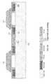
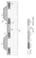
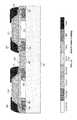
- FIG. 1is a multilevel device package according to one embodiment of the present invention.
- FIG. 2is an overview of processing used to form the package of FIG. 1
- FIGS. 2A-2Mare enlarged portions of the corresponding aspects of FIG. 2 .
- FIG. 3depicts the application of underfill material and optional heat sink and thermal interface material.
- FIG. 4depicts a heat-dissipation package structure for the multilevel device of FIG. 1 .
- FIG. 5depicts horizontal integration of semiconductor chips packaged according to the present invention.
- FIG. 1depicts a wafer-level device package according to one embodiment of the present invention.
- packaging of individual devices at the wafer levelavoids device contamination by particulates generated during device separation (e.g., dicing). That is, a finished, encapsulated device is formed prior to division into discrete devices such that particulates cannot reach the individual semiconductor chips.
- an image sensor “system on chip” 100is depicted; however, the features described in connection with FIG. 1 are applicable to single layer (that is, not vertically-integrated) device packages as will be discussed below.
- an imaging devicesuch as CMOS image sensor 110 has bonding pads 120 positioned thereon.
- metal studs 130are positioned over the bonding pads 120 to provide additional heat sink capabilities and/or to increase the clearance over image sensor 110 .
- the additional clearance from the metal studspermits formation of lens array 200 over the image sensor.
- a protective layer 140is bonded to the image sensor 110 through the bonding pads 120 /metal studs 130 structure.
- protective layer 140is a transparent material such as glass, fused silica, or alumina. Transparent polymer layers can also be used. For non-imaging applications, layer 140 need not be transparent.
- An insulation material 160covers at least the side and bottom surfaces of imaging device 110 .
- the insulation material 160also covers selected portions of the bonding pad 120 .
- Under bump metallization 170contacts bonding pad 120 to form an electrical connection therewith.
- Electrical connection bump 180such as a solder bump, is formed on the under bump metallization 170 .
- the optional insulation material 160 on the bonding padassists in formation of the under bump metallization (discussed below) and provides structural support.
- FIG. 2provides an overview of an exemplary fabrication process for the vertically-integrated device of FIG. 1 .
- Each sub-figure, labeled 2 A- 2 Mis reproduced in larger format following FIG. 2 so that the various device structures can be more easily seen.
- a protective layer/protective substrate 140is provided. As discussed above, for imaging sensor packages, the material of layer 140 is substantially transparent such as glass, silica, alumina, or a polymer.
- the material of layer 140is substantially transparent such as glass, silica, alumina, or a polymer.
- optional metal studs 130are deposited on layer 140 , followed by deposition of polymer coating 190 .
- Polymer coating 190is patterned in FIG. 2D to substantially surround metal studs 130 and provide electrical isolation therefor.
- a silicon wafer 110is bonded to the structure of FIG. 2D in the process of 2 E.
- Silicon waferincludes a plurality of semiconductor devices formed therein; note that device formation can take place before the bonding to layer 140 . Although device formation typically occurs before bonding to layer 140 , it is possible to fabricate devices in the semiconductor/silicon wafer after bonding.
- Silicon wafer 110includes oxide layer 115 and bonding pads 120 and is bonded directly or through an intermediate adhesive layer to the structure of FIG. 2D .
- Exemplary adhesivesinclude solder-based adhesives and conductive epoxy-based adhesives.
- the silicon waferis thinned in FIG. 2F , typically by chemical-mechanical polishing although any chemical, mechanical, or combined removal technique may be used. Note that devices may be formed in the silicon wafer following wafer thinning.
- trenches 210are etched between adjacent devices 110 ′ in FIG. 2G .
- Anisotropic etchingcan be used to form trenches 210 (e.g., wet etching) or isotropic etching can be used.
- the oxide layer 115 in the trench regionis removed in 2 H. Depending upon the trench formation in 2 G, the oxide layer 115 may be removed when the trench is created.
- a polymer layer 160is deposited, covering the sides and the bottom of what will eventually be individual semiconductor chips.
- the polymer layer 160covers portions of the bonding pads 120 that are not covered by the individual devices 110 ′ as seen in FIG. 2I .
- openings 230are created in polymer layer 160 in 2 J.
- An exemplary technique for forming openings 230is by laser drilling with a CO 2 laser; however, other etching or ablation techniques can be used to form the openings.
- under bump metallization layer 170is formed.
- electroless plating techniquescan be used to form the under bump metallization 170 with the remaining polymer walls 160 a providing mechanical reinforcement for the layer.
- Nickel and gold electroless platingcan be used to form under bump metallization 170 in FIG. 2K ; these materials provide a solder-wettable surface for subsequent solder bump formation.
- solder 180is deposited over the under bump metallization in FIG. 2L followed by reflow in FIG. 2M to form solder balls 180 .
- the solder bumpallows a greater alignment tolerance while at the same time maintaining the gap between vertically-stacked device chips.
- Underfill material 270is applied to the multi-layer structure to protect the structure and provide mechanical support.
- An optional heat sink 280such as a copper plate, can be embedded in a substrate 290 such as a printed circuit board. Thermal contact between the vertical stack and the heat sink 280 is provided by thermal interface material 285 .
- Device separationcan be performed through any dicing technique along dotted line 250 in FIG. 2M when a single layer device or series of devices is to be the final configuration.
- the above processesmay be repeated for additional wafers (e.g., digital signal processing wafer and memory wafer) and device separation performed following the vertical stack formation.
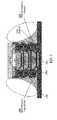
- FIG. 4An alternative electrical interface packaging structure is depicted in FIG. 4 .
- a flexible printed circuit board structure 320surrounds the multilevel chip structure, optionally including underfill material 270 . Copper connections 310 and copper pad 300 interconnect with solder bumps 180 and the flexible printed circuit board 320 .
- this packaging techniquecan also assist with heat dissipation through the various metallization layers.
- copper studs 130are replaced by additional solder bumps 390 and under bump metallizations 370 during fabrication of an array of devices 110 .
Landscapes
- Engineering & Computer Science (AREA)
- Microelectronics & Electronic Packaging (AREA)
- Power Engineering (AREA)
- Computer Hardware Design (AREA)
- Manufacturing & Machinery (AREA)
- Physics & Mathematics (AREA)
- Condensed Matter Physics & Semiconductors (AREA)
- General Physics & Mathematics (AREA)
- Solid State Image Pick-Up Elements (AREA)
Abstract
Description
Claims (12)
Priority Applications (2)
| Application Number | Priority Date | Filing Date | Title |
|---|---|---|---|
| US13/551,610US9117715B2 (en) | 2012-07-18 | 2012-07-18 | Wafer-level device packaging |
| CN201210295014.1ACN102881666B (en) | 2012-07-18 | 2012-08-17 | wafer level device package |
Applications Claiming Priority (1)
| Application Number | Priority Date | Filing Date | Title |
|---|---|---|---|
| US13/551,610US9117715B2 (en) | 2012-07-18 | 2012-07-18 | Wafer-level device packaging |
Publications (2)
| Publication Number | Publication Date |
|---|---|
| US20140021596A1 US20140021596A1 (en) | 2014-01-23 |
| US9117715B2true US9117715B2 (en) | 2015-08-25 |
Family
ID=47482941
Family Applications (1)
| Application Number | Title | Priority Date | Filing Date |
|---|---|---|---|
| US13/551,610Expired - Fee RelatedUS9117715B2 (en) | 2012-07-18 | 2012-07-18 | Wafer-level device packaging |
Country Status (2)
| Country | Link |
|---|---|
| US (1) | US9117715B2 (en) |
| CN (1) | CN102881666B (en) |
Families Citing this family (5)
| Publication number | Priority date | Publication date | Assignee | Title |
|---|---|---|---|---|
| CN103762202B (en)* | 2014-01-28 | 2017-04-19 | 苏州晶方半导体科技股份有限公司 | Chip packaging method and structure |
| US9087759B1 (en) | 2014-03-28 | 2015-07-21 | Taiwan Semiconductor Manufacturing Co., Ltd. | Method of forming an image sensor device and method of forming the same |
| CN104332452B (en)* | 2014-08-20 | 2017-04-19 | 深圳市汇顶科技股份有限公司 | Chip packaging module |
| KR102492527B1 (en)* | 2015-10-12 | 2023-01-31 | 삼성전자주식회사 | data storage device and electric apparatus including the same |
| CN108615772B (en)* | 2018-05-17 | 2020-05-12 | 中国科学院微电子研究所 | Packaging structure of sensor and manufacturing method thereof |
Citations (29)
| Publication number | Priority date | Publication date | Assignee | Title |
|---|---|---|---|---|
| US3761782A (en)* | 1971-05-19 | 1973-09-25 | Signetics Corp | Semiconductor structure, assembly and method |
| US5229647A (en)* | 1991-03-27 | 1993-07-20 | Micron Technology, Inc. | High density data storage using stacked wafers |
| US6221751B1 (en)* | 1997-01-24 | 2001-04-24 | Chipscale, Inc. | Wafer fabrication of die-bottom contacts for electronic devices |
| US6235554B1 (en)* | 1995-11-27 | 2001-05-22 | Micron Technology, Inc. | Method for fabricating stackable chip scale semiconductor package |
| US6312974B1 (en) | 2000-10-26 | 2001-11-06 | Industrial Technology Research Institute | Simultaneous bumping/bonding process utilizing edge-type conductive pads and device fabricated |
| JP2002329852A (en) | 2001-05-01 | 2002-11-15 | Fuji Film Microdevices Co Ltd | Solid-state imaging device and method of manufacturing the same |
| US20040235270A1 (en)* | 2002-04-23 | 2004-11-25 | Sanyo Electric Co., Ltd. | Method of manufacturing semiconductor device |
| US6841883B1 (en)* | 2003-03-31 | 2005-01-11 | Micron Technology, Inc. | Multi-dice chip scale semiconductor components and wafer level methods of fabrication |
| US6884650B2 (en) | 2002-11-14 | 2005-04-26 | Samsung Electronics Co., Ltd. | Side-bonding method of flip-chip semiconductor device, MEMS device package and package method using the same |
| US20060091488A1 (en) | 2004-11-01 | 2006-05-04 | Dongbuanam Semiconductor Inc. | Image sensor chip package and method of fabricating the same |
| US20070069394A1 (en)* | 2005-09-27 | 2007-03-29 | Agere Systems Inc. | Solder bump structure for flip chip semiconductor devices and method of manufacture therefore |
| US20070216028A1 (en)* | 2006-03-14 | 2007-09-20 | Samsung Electronics Co., Ltd. | Micro-element package and manufacturing method thereof |
| US20070264757A1 (en)* | 2005-07-15 | 2007-11-15 | Kwon Jong-Oh | Micro-package, multi-stack micro-package, and manufacturing method therefor |
| US7394152B2 (en) | 2006-11-13 | 2008-07-01 | China Wafer Level Csp Ltd. | Wafer level chip size packaged chip device with an N-shape junction inside and method of fabricating the same |
| US20080157340A1 (en)* | 2006-12-29 | 2008-07-03 | Advanced Chip Engineering Technology Inc. | RF module package |
| US20080224306A1 (en)* | 2007-01-03 | 2008-09-18 | Wen-Kun Yang | Multi-chips package and method of forming the same |
| CN101304015A (en) | 2007-05-07 | 2008-11-12 | 三洋电机株式会社 | Semiconductor device and manufacturing method thereof |
| CN101356645A (en) | 2005-10-11 | 2009-01-28 | 朴太锡 | Method for encapsulating and manufacturing CMOS image sensor wafer using silicium through-hole contact point |
| US20090224402A1 (en)* | 2008-03-07 | 2009-09-10 | Stats Chippac, Ltd. | Semiconductor Package Having Semiconductor Die with Internal Vertical Interconnect Structure and Method Therefor |
| US20090243083A1 (en)* | 2008-03-25 | 2009-10-01 | Stats Chippac, Ltd. | Wafer Integrated with Permanent Carrier and Method Therefor |
| US20090283903A1 (en)* | 2005-12-02 | 2009-11-19 | Nepes Corporation | Bump with multiple vias for semiconductor package and fabrication method thereof, and semiconductor package utilizing the same |
| US20100013102A1 (en)* | 2008-07-15 | 2010-01-21 | Stats Chippac, Ltd. | Semiconductor Device and Method of Providing a Thermal Dissipation Path Through RDL and Conductive Via |
| US20110018117A1 (en)* | 2009-07-24 | 2011-01-27 | Industrial Technology Research Institute | Sealed joint structure of device and process using the same |
| US7989356B2 (en) | 2009-03-24 | 2011-08-02 | Stats Chippac, Ltd. | Semiconductor device and method of forming enhanced UBM structure for improving solder joint reliability |
| US20110215449A1 (en)* | 2010-03-08 | 2011-09-08 | Stats Chippac, Ltd. | Semiconductor Device and Method of Forming Wafer Level Multi-Row Etched Lead Package |
| US20120012997A1 (en)* | 2010-07-13 | 2012-01-19 | Taiwan Semiconductor Manufacturing Company, Ltd. | Recessed Pillar Structure |
| US20120049334A1 (en)* | 2010-08-27 | 2012-03-01 | Stats Chippac, Ltd. | Semiconductor Device and Method of Forming Leadframe as Vertical Interconnect Structure Between Stacked Semiconductor Die |
| US20140151900A1 (en)* | 2011-12-14 | 2014-06-05 | Broadcom Corporation | Stacked packaging using reconstituted wafers |
| US20140167253A1 (en)* | 2012-04-17 | 2014-06-19 | Taiwan Semiconductor Manufacturing Company, Ltd. | Semiconductor Devices, Methods of Manufacture Thereof, and Packaged Semiconductor Devices |
- 2012
- 2012-07-18USUS13/551,610patent/US9117715B2/ennot_activeExpired - Fee Related
- 2012-08-17CNCN201210295014.1Apatent/CN102881666B/ennot_activeExpired - Fee Related
Patent Citations (30)
| Publication number | Priority date | Publication date | Assignee | Title |
|---|---|---|---|---|
| US3761782A (en)* | 1971-05-19 | 1973-09-25 | Signetics Corp | Semiconductor structure, assembly and method |
| US5229647A (en)* | 1991-03-27 | 1993-07-20 | Micron Technology, Inc. | High density data storage using stacked wafers |
| US6235554B1 (en)* | 1995-11-27 | 2001-05-22 | Micron Technology, Inc. | Method for fabricating stackable chip scale semiconductor package |
| US6221751B1 (en)* | 1997-01-24 | 2001-04-24 | Chipscale, Inc. | Wafer fabrication of die-bottom contacts for electronic devices |
| US6312974B1 (en) | 2000-10-26 | 2001-11-06 | Industrial Technology Research Institute | Simultaneous bumping/bonding process utilizing edge-type conductive pads and device fabricated |
| JP2002329852A (en) | 2001-05-01 | 2002-11-15 | Fuji Film Microdevices Co Ltd | Solid-state imaging device and method of manufacturing the same |
| US20040235270A1 (en)* | 2002-04-23 | 2004-11-25 | Sanyo Electric Co., Ltd. | Method of manufacturing semiconductor device |
| US6884650B2 (en) | 2002-11-14 | 2005-04-26 | Samsung Electronics Co., Ltd. | Side-bonding method of flip-chip semiconductor device, MEMS device package and package method using the same |
| US6841883B1 (en)* | 2003-03-31 | 2005-01-11 | Micron Technology, Inc. | Multi-dice chip scale semiconductor components and wafer level methods of fabrication |
| US20070132104A1 (en)* | 2003-03-31 | 2007-06-14 | Farnworth Warren M | Semiconductor component having plate, stacked dice and conductive vias |
| US20060091488A1 (en) | 2004-11-01 | 2006-05-04 | Dongbuanam Semiconductor Inc. | Image sensor chip package and method of fabricating the same |
| US20070264757A1 (en)* | 2005-07-15 | 2007-11-15 | Kwon Jong-Oh | Micro-package, multi-stack micro-package, and manufacturing method therefor |
| US20070069394A1 (en)* | 2005-09-27 | 2007-03-29 | Agere Systems Inc. | Solder bump structure for flip chip semiconductor devices and method of manufacture therefore |
| CN101356645A (en) | 2005-10-11 | 2009-01-28 | 朴太锡 | Method for encapsulating and manufacturing CMOS image sensor wafer using silicium through-hole contact point |
| US20090283903A1 (en)* | 2005-12-02 | 2009-11-19 | Nepes Corporation | Bump with multiple vias for semiconductor package and fabrication method thereof, and semiconductor package utilizing the same |
| US20070216028A1 (en)* | 2006-03-14 | 2007-09-20 | Samsung Electronics Co., Ltd. | Micro-element package and manufacturing method thereof |
| US7394152B2 (en) | 2006-11-13 | 2008-07-01 | China Wafer Level Csp Ltd. | Wafer level chip size packaged chip device with an N-shape junction inside and method of fabricating the same |
| US20080157340A1 (en)* | 2006-12-29 | 2008-07-03 | Advanced Chip Engineering Technology Inc. | RF module package |
| US20080224306A1 (en)* | 2007-01-03 | 2008-09-18 | Wen-Kun Yang | Multi-chips package and method of forming the same |
| CN101304015A (en) | 2007-05-07 | 2008-11-12 | 三洋电机株式会社 | Semiconductor device and manufacturing method thereof |
| US20090224402A1 (en)* | 2008-03-07 | 2009-09-10 | Stats Chippac, Ltd. | Semiconductor Package Having Semiconductor Die with Internal Vertical Interconnect Structure and Method Therefor |
| US20090243083A1 (en)* | 2008-03-25 | 2009-10-01 | Stats Chippac, Ltd. | Wafer Integrated with Permanent Carrier and Method Therefor |
| US20100013102A1 (en)* | 2008-07-15 | 2010-01-21 | Stats Chippac, Ltd. | Semiconductor Device and Method of Providing a Thermal Dissipation Path Through RDL and Conductive Via |
| US7989356B2 (en) | 2009-03-24 | 2011-08-02 | Stats Chippac, Ltd. | Semiconductor device and method of forming enhanced UBM structure for improving solder joint reliability |
| US20110018117A1 (en)* | 2009-07-24 | 2011-01-27 | Industrial Technology Research Institute | Sealed joint structure of device and process using the same |
| US20110215449A1 (en)* | 2010-03-08 | 2011-09-08 | Stats Chippac, Ltd. | Semiconductor Device and Method of Forming Wafer Level Multi-Row Etched Lead Package |
| US20120012997A1 (en)* | 2010-07-13 | 2012-01-19 | Taiwan Semiconductor Manufacturing Company, Ltd. | Recessed Pillar Structure |
| US20120049334A1 (en)* | 2010-08-27 | 2012-03-01 | Stats Chippac, Ltd. | Semiconductor Device and Method of Forming Leadframe as Vertical Interconnect Structure Between Stacked Semiconductor Die |
| US20140151900A1 (en)* | 2011-12-14 | 2014-06-05 | Broadcom Corporation | Stacked packaging using reconstituted wafers |
| US20140167253A1 (en)* | 2012-04-17 | 2014-06-19 | Taiwan Semiconductor Manufacturing Company, Ltd. | Semiconductor Devices, Methods of Manufacture Thereof, and Packaged Semiconductor Devices |
Non-Patent Citations (1)
| Title |
|---|
| Office Action issued from the State Intellectual Property Office of the People's Republic of China on Jul. 17, 2014. |
Also Published As
| Publication number | Publication date |
|---|---|
| US20140021596A1 (en) | 2014-01-23 |
| CN102881666B (en) | 2015-07-08 |
| CN102881666A (en) | 2013-01-16 |
Similar Documents
| Publication | Publication Date | Title |
|---|---|---|
| US10056419B2 (en) | Chip package having chip connected to sensing device with redistribution layer in insulator layer | |
| US10128223B2 (en) | Semiconductor device and manufacturing method thereof | |
| US9396998B2 (en) | Semiconductor device having fan-in and fan-out redistribution layers | |
| KR101640076B1 (en) | Stacked chip package and method for manufacturing the same | |
| CN103633075B (en) | Package-on-package semiconductor device | |
| US8922026B2 (en) | Chip package and fabrication method thereof | |
| CN101312200B (en) | Image sensing devices and methods for fabricating same | |
| US10157875B2 (en) | Chip package and method for forming the same | |
| CN214672598U (en) | Three-dimensional semiconductor device structure and three-dimensional semiconductor device | |
| CN109003961B (en) | 3D system integrated structure and manufacturing method thereof | |
| US11728279B2 (en) | Pad structure for enhanced bondability | |
| US12412802B2 (en) | Heat dissipation structures for integrated circuit packages and methods of forming the same | |
| TW201803056A (en) | Semiconductor package and method of manufacturing same | |
| KR20160032718A (en) | A chip arrangement and a method for manufacturing a chip arrangement | |
| WO2015183959A1 (en) | Structure and method for integrated circuits packaging with increased density | |
| JP2009088459A (en) | Wafer level image sensor module, manufacturing method thereof, and camera module | |
| US9117715B2 (en) | Wafer-level device packaging | |
| JP2009099841A (en) | Semiconductor device and manufacturing method thereof | |
| US20240258277A1 (en) | Semiconductor packages and method for fabricating the same | |
| US10243017B2 (en) | Sensor chip stack and method of producing a sensor chip stack |
Legal Events
| Date | Code | Title | Description |
|---|---|---|---|
| AS | Assignment | Owner name:HONG KONG APPLIED SCIENCE AND TECHNOLOGY RESEARCH Free format text:ASSIGNMENT OF ASSIGNORS INTEREST;ASSIGNORS:TSUI, YAT KIT;YANG, DAN;LAW, PUI CHUNG;SIGNING DATES FROM 20120716 TO 20120717;REEL/FRAME:028571/0085 | |
| ZAAA | Notice of allowance and fees due | Free format text:ORIGINAL CODE: NOA | |
| ZAAB | Notice of allowance mailed | Free format text:ORIGINAL CODE: MN/=. | |
| ZAAA | Notice of allowance and fees due | Free format text:ORIGINAL CODE: NOA | |
| STCF | Information on status: patent grant | Free format text:PATENTED CASE | |
| MAFP | Maintenance fee payment | Free format text:PAYMENT OF MAINTENANCE FEE, 4TH YEAR, LARGE ENTITY (ORIGINAL EVENT CODE: M1551); ENTITY STATUS OF PATENT OWNER: LARGE ENTITY Year of fee payment:4 | |
| FEPP | Fee payment procedure | Free format text:MAINTENANCE FEE REMINDER MAILED (ORIGINAL EVENT CODE: REM.); ENTITY STATUS OF PATENT OWNER: LARGE ENTITY | |
| LAPS | Lapse for failure to pay maintenance fees | Free format text:PATENT EXPIRED FOR FAILURE TO PAY MAINTENANCE FEES (ORIGINAL EVENT CODE: EXP.); ENTITY STATUS OF PATENT OWNER: LARGE ENTITY | |
| STCH | Information on status: patent discontinuation | Free format text:PATENT EXPIRED DUE TO NONPAYMENT OF MAINTENANCE FEES UNDER 37 CFR 1.362 | |
| FP | Lapsed due to failure to pay maintenance fee | Effective date:20230825 |