US9116823B2 - Systems and methods for adaptive error-correction coding - Google Patents
Systems and methods for adaptive error-correction codingDownload PDFInfo
- Publication number
- US9116823B2 US9116823B2US13/830,652US201313830652AUS9116823B2US 9116823 B2US9116823 B2US 9116823B2US 201313830652 AUS201313830652 AUS 201313830652AUS 9116823 B2US9116823 B2US 9116823B2
- Authority
- US
- United States
- Prior art keywords
- data
- ecc
- solid
- state storage
- module
- Prior art date
- Legal status (The legal status is an assumption and is not a legal conclusion. Google has not performed a legal analysis and makes no representation as to the accuracy of the status listed.)
- Active, expires
Links
Images


Classifications
- G—PHYSICS
- G06—COMPUTING OR CALCULATING; COUNTING
- G06F—ELECTRIC DIGITAL DATA PROCESSING
- G06F11/00—Error detection; Error correction; Monitoring
- G06F11/07—Responding to the occurrence of a fault, e.g. fault tolerance
- G06F11/08—Error detection or correction by redundancy in data representation, e.g. by using checking codes
- G06F11/10—Adding special bits or symbols to the coded information, e.g. parity check, casting out 9's or 11's
- G—PHYSICS
- G06—COMPUTING OR CALCULATING; COUNTING
- G06F—ELECTRIC DIGITAL DATA PROCESSING
- G06F12/00—Accessing, addressing or allocating within memory systems or architectures
- G06F12/02—Addressing or allocation; Relocation
- G06F12/0223—User address space allocation, e.g. contiguous or non contiguous base addressing
- G06F12/023—Free address space management
- G06F12/0253—Garbage collection, i.e. reclamation of unreferenced memory
- G—PHYSICS
- G06—COMPUTING OR CALCULATING; COUNTING
- G06F—ELECTRIC DIGITAL DATA PROCESSING
- G06F11/00—Error detection; Error correction; Monitoring
- G06F11/07—Responding to the occurrence of a fault, e.g. fault tolerance
- G06F11/08—Error detection or correction by redundancy in data representation, e.g. by using checking codes
- G06F11/10—Adding special bits or symbols to the coded information, e.g. parity check, casting out 9's or 11's
- G06F11/1008—Adding special bits or symbols to the coded information, e.g. parity check, casting out 9's or 11's in individual solid state devices
- G06F11/1068—Adding special bits or symbols to the coded information, e.g. parity check, casting out 9's or 11's in individual solid state devices in sector programmable memories, e.g. flash disk
- G—PHYSICS
- G06—COMPUTING OR CALCULATING; COUNTING
- G06F—ELECTRIC DIGITAL DATA PROCESSING
- G06F11/00—Error detection; Error correction; Monitoring
- G06F11/07—Responding to the occurrence of a fault, e.g. fault tolerance
- G06F11/08—Error detection or correction by redundancy in data representation, e.g. by using checking codes
- G06F11/10—Adding special bits or symbols to the coded information, e.g. parity check, casting out 9's or 11's
- G06F11/1008—Adding special bits or symbols to the coded information, e.g. parity check, casting out 9's or 11's in individual solid state devices
- G06F11/1044—Adding special bits or symbols to the coded information, e.g. parity check, casting out 9's or 11's in individual solid state devices with specific ECC/EDC distribution
- G—PHYSICS
- G06—COMPUTING OR CALCULATING; COUNTING
- G06F—ELECTRIC DIGITAL DATA PROCESSING
- G06F11/00—Error detection; Error correction; Monitoring
- G06F11/07—Responding to the occurrence of a fault, e.g. fault tolerance
- G06F11/08—Error detection or correction by redundancy in data representation, e.g. by using checking codes
- G06F11/10—Adding special bits or symbols to the coded information, e.g. parity check, casting out 9's or 11's
- G06F11/1076—Parity data used in redundant arrays of independent storages, e.g. in RAID systems
- G06F11/108—Parity data distribution in semiconductor storages, e.g. in SSD
- G—PHYSICS
- G06—COMPUTING OR CALCULATING; COUNTING
- G06F—ELECTRIC DIGITAL DATA PROCESSING
- G06F3/00—Input arrangements for transferring data to be processed into a form capable of being handled by the computer; Output arrangements for transferring data from processing unit to output unit, e.g. interface arrangements
- G06F3/06—Digital input from, or digital output to, record carriers, e.g. RAID, emulated record carriers or networked record carriers
- G06F3/0601—Interfaces specially adapted for storage systems
- G06F3/0602—Interfaces specially adapted for storage systems specifically adapted to achieve a particular effect
- G06F3/0614—Improving the reliability of storage systems
- G06F3/0619—Improving the reliability of storage systems in relation to data integrity, e.g. data losses, bit errors
- G—PHYSICS
- G06—COMPUTING OR CALCULATING; COUNTING
- G06F—ELECTRIC DIGITAL DATA PROCESSING
- G06F3/00—Input arrangements for transferring data to be processed into a form capable of being handled by the computer; Output arrangements for transferring data from processing unit to output unit, e.g. interface arrangements
- G06F3/06—Digital input from, or digital output to, record carriers, e.g. RAID, emulated record carriers or networked record carriers
- G06F3/0601—Interfaces specially adapted for storage systems
- G06F3/0628—Interfaces specially adapted for storage systems making use of a particular technique
- G06F3/0638—Organizing or formatting or addressing of data
- G06F3/064—Management of blocks
- G—PHYSICS
- G06—COMPUTING OR CALCULATING; COUNTING
- G06F—ELECTRIC DIGITAL DATA PROCESSING
- G06F3/00—Input arrangements for transferring data to be processed into a form capable of being handled by the computer; Output arrangements for transferring data from processing unit to output unit, e.g. interface arrangements
- G06F3/06—Digital input from, or digital output to, record carriers, e.g. RAID, emulated record carriers or networked record carriers
- G06F3/0601—Interfaces specially adapted for storage systems
- G06F3/0668—Interfaces specially adapted for storage systems adopting a particular infrastructure
- G06F3/0671—In-line storage system
- G06F3/0673—Single storage device
- G06F3/0679—Non-volatile semiconductor memory device, e.g. flash memory, one time programmable memory [OTP]
- G—PHYSICS
- G06—COMPUTING OR CALCULATING; COUNTING
- G06F—ELECTRIC DIGITAL DATA PROCESSING
- G06F9/00—Arrangements for program control, e.g. control units
- G06F9/06—Arrangements for program control, e.g. control units using stored programs, i.e. using an internal store of processing equipment to receive or retain programs
- G06F9/46—Multiprogramming arrangements
- G06F9/52—Program synchronisation; Mutual exclusion, e.g. by means of semaphores
- G—PHYSICS
- G11—INFORMATION STORAGE
- G11C—STATIC STORES
- G11C29/00—Checking stores for correct operation ; Subsequent repair; Testing stores during standby or offline operation
- G11C29/52—Protection of memory contents; Detection of errors in memory contents
- H—ELECTRICITY
- H03—ELECTRONIC CIRCUITRY
- H03M—CODING; DECODING; CODE CONVERSION IN GENERAL
- H03M13/00—Coding, decoding or code conversion, for error detection or error correction; Coding theory basic assumptions; Coding bounds; Error probability evaluation methods; Channel models; Simulation or testing of codes
- H03M13/35—Unequal or adaptive error protection, e.g. by providing a different level of protection according to significance of source information or by adapting the coding according to the change of transmission channel characteristics
- H03M13/353—Adaptation to the channel
- H—ELECTRICITY
- H04—ELECTRIC COMMUNICATION TECHNIQUE
- H04L—TRANSMISSION OF DIGITAL INFORMATION, e.g. TELEGRAPHIC COMMUNICATION
- H04L12/00—Data switching networks
- H04L12/28—Data switching networks characterised by path configuration, e.g. LAN [Local Area Networks] or WAN [Wide Area Networks]
- H04L12/46—Interconnection of networks
- H04L12/4604—LAN interconnection over a backbone network, e.g. Internet, Frame Relay
- H04L12/462—LAN interconnection over a bridge based backbone
- H04L12/4625—Single bridge functionality, e.g. connection of two networks over a single bridge
- H—ELECTRICITY
- H04—ELECTRIC COMMUNICATION TECHNIQUE
- H04L—TRANSMISSION OF DIGITAL INFORMATION, e.g. TELEGRAPHIC COMMUNICATION
- H04L12/00—Data switching networks
- H04L12/64—Hybrid switching systems
- H04L12/6418—Hybrid transport
- G—PHYSICS
- G06—COMPUTING OR CALCULATING; COUNTING
- G06F—ELECTRIC DIGITAL DATA PROCESSING
- G06F2211/00—Indexing scheme relating to details of data-processing equipment not covered by groups G06F3/00 - G06F13/00
- G06F2211/10—Indexing scheme relating to G06F11/10
- G06F2211/1002—Indexing scheme relating to G06F11/1076
- G06F2211/109—Sector level checksum or ECC, i.e. sector or stripe level checksum or ECC in addition to the RAID parity calculation
- G—PHYSICS
- G06—COMPUTING OR CALCULATING; COUNTING
- G06F—ELECTRIC DIGITAL DATA PROCESSING
- G06F2212/00—Indexing scheme relating to accessing, addressing or allocation within memory systems or architectures
- G06F2212/20—Employing a main memory using a specific memory technology
- G06F2212/202—Non-volatile memory
- G06F2212/2022—Flash memory
- H—ELECTRICITY
- H04—ELECTRIC COMMUNICATION TECHNIQUE
- H04L—TRANSMISSION OF DIGITAL INFORMATION, e.g. TELEGRAPHIC COMMUNICATION
- H04L67/00—Network arrangements or protocols for supporting network services or applications
- H04L67/01—Protocols
- H04L67/10—Protocols in which an application is distributed across nodes in the network
- H04L67/1097—Protocols in which an application is distributed across nodes in the network for distributed storage of data in networks, e.g. transport arrangements for network file system [NFS], storage area networks [SAN] or network attached storage [NAS]
Definitions
- FIG. 11is a flow diagram of another embodiment of a method for adaptive storage on a solid-state storage array
- FIG. 15is a flow diagram of one embodiment of a method for adaptive data storage using ECC codeword symbols
- a data segmentrefers to a quantum of structured or unstructured data; a data segment may, therefore, include, but is not limited to: data pertaining to a storage request, data corresponding to one or more logical identifiers, one or more data blocks, a data structure, such as a data packet, container, or the like, a data set, such as a data range, extent, or the like, an ECC codeword, such as an ECC syndrome, an ECC symbol, an ECC chunk, or the like, unstructured data, structured data, a data record, or the like.
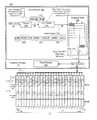
- the write module 240further comprises a write buffer 250 configured to buffer data for storage within respective page write buffers of the solid-state storage medium 110 .
- the write buffer 250may comprise one or more synchronization buffers to synchronize a clock domain of the adaptive storage module 113 with a clock domain of the solid-state storage medium 110 (and/or bus 127 ).
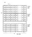
- the columns 118 of the array 115may correspond to respective solid-state storage elements 116 A-Y. Accordingly, the array 115 of FIG. 5A comprises 25 columns 118 . Rows of the array 117 may correspond to physical storage units 532 and/or 530 of a plurality of the columns 118 .
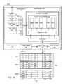
- the adaptive write module 248may be configured to buffer six (6) ECC codewords 620 in a four-column adaptive channel configuration (e.g., store ECC codewords 620 across each of four columns), buffer four ECC codewords 620 in a six-column adaptive channel configuration (e.g. store ECC codewords 620 across each of six columns), and so on.
- each ECC codeword 620(e.g., ECC codewords 621 , 622 , 623 , 629 , and so on) are transferred to program buffers of respective solid-state storage elements 116 A-X.
- the source of the errormay be immediately determined without iterative parity substitution; since all of the data of the ECC codeword 620 is stored within a single solid-state storage element 116 A-X, failure to validate an ECC codeword 620 by the ECC read module 245 indicates that the corresponding column 118 within the array 115 is the source of the uncorrectable error.
- T sChannels
- T s240- 960-Byte Codewords/ Byte Data Data Adaptive Data Configuration Read Structures Structures 1 of 24 (vertical, FIGS. 6C and 1 240 960 6D) 2 of 12 (hybrid, FIGS.
- the adaptive write module 248is configured to divide the solid-state storage array 115 into a set of independent channels 696 A-N, each of which comprises a set of four columns 118 : channel 696 A comprises solid-state storage elements 116 A-D, channel 696 B comprises solid-state storage elements 116 E-H, channel 696 N comprises solid-state storage elements 116 U-X, and so on.
- the set of ECC codeword symbols 630 A comprising packet 610 Aare configured for storage in channel 696 A
- the set of ECC codeword symbols 630 B comprising packet 610 Bare configured to storage in channel 696 B
- the ECC codeword symbols 630 N comprising packet 610 Nare configured to storage in channel 696 N, and so on.
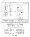
- Step 1650may comprise identifying an ECC codeword symbol 630 that is unavailable due to, inter alia, an uncorrectable error in the ECC codeword symbol 630 , read failure, hardware fault, and/or the like.
- the flowmay continue at step 1652 in response to detecting the unavailable ECC codeword symbol; otherwise, the flow may continue at step 1660 .
Landscapes
- Engineering & Computer Science (AREA)
- Theoretical Computer Science (AREA)
- Physics & Mathematics (AREA)
- General Engineering & Computer Science (AREA)
- General Physics & Mathematics (AREA)
- Quality & Reliability (AREA)
- Signal Processing (AREA)
- Computer Networks & Wireless Communication (AREA)
- Software Systems (AREA)
- Human Computer Interaction (AREA)
- Probability & Statistics with Applications (AREA)
- Computer Security & Cryptography (AREA)
- Techniques For Improving Reliability Of Storages (AREA)
Abstract
Description
| Independent | Ts: | |||
| Channels, | Ts: 240- | 960-Byte | ||
| Codewords/ | Byte Data | Data | ||
| Adaptive Data Configuration | Structures | Structures | ||
| 1 of 24 (vertical, FIGS. 6C and | 1 | 240 | 960 |
| 6D) | |||
| 2 of 12 (hybrid, FIGS. 6E and 6F) | 2 | 120 | 480 |
| 3 of 8 | 3 | 80 | 320 |
| 4 of 6 | 4 | 60 | 240 |
| 2 of 3 and 3 of 6 | 5 | 48 | 192 |
| 6 of 4 | 6 | 40 | 160 |
| 4 of 3 and 3 of 4 | 7 | 34 | 137 |
| 8 of 3 | 8 | 30 | 120 |
| 4 of 3 and 5 of 2 and extra 2 of 1 | 9 | 27 | 107 |
| 4 of 3 and 6 of 2 | 10 | 24 | 96 |
| 4 of 3 and 5 of 2 and 2 of 1 | 11 | 22 | 87 |
| 12 of 2 | 12 | 20 | 80 |
| 4 of 3 and 3 of 2 and 6 of 1 | 13 | 18 | 74 |
| 4 of 3 and 2 of 2 and 8 of 1 | 14 | 17 | 69 |
| 4 of 3 and 1 of 2 and 10 of 1 | 15 | 16 | 64 |
| 4 of 3 and 12 of 1 | 16 | 15 | 60 |
| 3 of 3 and 14 of 1 and extra 1 of 1 | 17 | 14 | 56 |
| 3 of 3 and 15 of 1 | 18 | 13 | 53 |
| 2 of 3 and 18 of 1 | 20 | 12 | 48 |
| 1 of 3 and 20 of 1 and extra 1 of 1 | 21 | 11 | 46 |
| 1 of 3 and 21 of 1 | 22 | 11 | 44 |
| 1 of 2 and 22 of 1 | 23 | 10 | 42 |
| 24 of 1 (horizontal, FIGS. 6A and | 24 | 10 | 40 |
| 6B) | |||
Claims (18)
Priority Applications (4)
| Application Number | Priority Date | Filing Date | Title |
|---|---|---|---|
| US13/830,652US9116823B2 (en) | 2006-12-06 | 2013-03-14 | Systems and methods for adaptive error-correction coding |
| US14/807,526US20150333773A1 (en) | 2006-12-06 | 2015-07-23 | Systems and methods for adaptive error-correction coding |
| US15/253,334US11061765B2 (en) | 2006-12-06 | 2016-08-31 | Systems and methods for adaptive error-correction coding |
| US17/340,355US20210342223A1 (en) | 2006-12-06 | 2021-06-07 | Systems and methods for adaptive error-correction coding |
Applications Claiming Priority (8)
| Application Number | Priority Date | Filing Date | Title |
|---|---|---|---|
| US87311106P | 2006-12-06 | 2006-12-06 | |
| US97447007P | 2007-09-22 | 2007-09-22 | |
| US11/952,101US8402201B2 (en) | 2006-12-06 | 2007-12-06 | Apparatus, system, and method for storage space recovery in solid-state storage |
| US13/296,834US20140289447A9 (en) | 2006-12-06 | 2011-11-15 | Apparatus, system, and method for storage space recovery |
| US201261606253P | 2012-03-02 | 2012-03-02 | |
| US201261606755P | 2012-03-05 | 2012-03-05 | |
| US13/784,705US9495241B2 (en) | 2006-12-06 | 2013-03-04 | Systems and methods for adaptive data storage |
| US13/830,652US9116823B2 (en) | 2006-12-06 | 2013-03-14 | Systems and methods for adaptive error-correction coding |
Related Parent Applications (1)
| Application Number | Title | Priority Date | Filing Date |
|---|---|---|---|
| US13/784,705Continuation-In-PartUS9495241B2 (en) | 2006-12-06 | 2013-03-04 | Systems and methods for adaptive data storage |
Related Child Applications (1)
| Application Number | Title | Priority Date | Filing Date |
|---|---|---|---|
| US14/807,526ContinuationUS20150333773A1 (en) | 2006-12-06 | 2015-07-23 | Systems and methods for adaptive error-correction coding |
Publications (2)
| Publication Number | Publication Date |
|---|---|
| US20130205183A1 US20130205183A1 (en) | 2013-08-08 |
| US9116823B2true US9116823B2 (en) | 2015-08-25 |
Family
ID=48903997
Family Applications (4)
| Application Number | Title | Priority Date | Filing Date |
|---|---|---|---|
| US13/830,652Active2027-12-11US9116823B2 (en) | 2006-12-06 | 2013-03-14 | Systems and methods for adaptive error-correction coding |
| US14/807,526AbandonedUS20150333773A1 (en) | 2006-12-06 | 2015-07-23 | Systems and methods for adaptive error-correction coding |
| US15/253,334Active2028-03-25US11061765B2 (en) | 2006-12-06 | 2016-08-31 | Systems and methods for adaptive error-correction coding |
| US17/340,355AbandonedUS20210342223A1 (en) | 2006-12-06 | 2021-06-07 | Systems and methods for adaptive error-correction coding |
Family Applications After (3)
| Application Number | Title | Priority Date | Filing Date |
|---|---|---|---|
| US14/807,526AbandonedUS20150333773A1 (en) | 2006-12-06 | 2015-07-23 | Systems and methods for adaptive error-correction coding |
| US15/253,334Active2028-03-25US11061765B2 (en) | 2006-12-06 | 2016-08-31 | Systems and methods for adaptive error-correction coding |
| US17/340,355AbandonedUS20210342223A1 (en) | 2006-12-06 | 2021-06-07 | Systems and methods for adaptive error-correction coding |
Country Status (1)
| Country | Link |
|---|---|
| US (4) | US9116823B2 (en) |
Cited By (10)
| Publication number | Priority date | Publication date | Assignee | Title |
|---|---|---|---|---|
| US20160110125A1 (en)* | 2014-10-20 | 2016-04-21 | Fusion-Io, Inc. | Storage error management |
| US20160119080A1 (en)* | 2014-10-24 | 2016-04-28 | Thales | Method and system for processing data in a telecommunications system for dynamic adaptation to the quantity of data to be transmitted |
| US20170017542A1 (en)* | 2006-12-06 | 2017-01-19 | Longitude Enterprise Flash S.A.R.L. | Systems and methods for adaptive data storage |
| US9852025B2 (en) | 2016-03-29 | 2017-12-26 | Alibaba Group Holding Limited | Protecting data stored on a solid state drive |
| US10180875B2 (en) | 2016-07-08 | 2019-01-15 | Toshiba Memory Corporation | Pool-level solid state drive error correction |
| US20190303238A1 (en)* | 2018-03-28 | 2019-10-03 | Samsung Electronics Co., Ltd. | Band dram ecc |
| US20190318798A1 (en)* | 2018-04-12 | 2019-10-17 | Micron Technology, Inc. | Defective Memory Unit Screening in a Memory System |
| US10545830B2 (en)* | 2017-02-06 | 2020-01-28 | Samsung Electronics Co., Ltd. | Storage device for processing corrupted metadata and method of operating the same |
| US11573909B2 (en) | 2006-12-06 | 2023-02-07 | Unification Technologies Llc | Apparatus, system, and method for managing commands of solid-state storage using bank interleave |
| US20240103969A1 (en)* | 2022-09-16 | 2024-03-28 | Netapp, Inc. | Data storage system drive utilization |
Families Citing this family (84)
| Publication number | Priority date | Publication date | Assignee | Title |
|---|---|---|---|---|
| GB2488462B (en)* | 2009-12-17 | 2018-01-17 | Ibm | Data management in solid state storage systems |
| JP2013542533A (en)* | 2010-10-27 | 2013-11-21 | エルエスアイ コーポレーション | Adaptive ECC technology for flash memory based data storage |
| US9318166B2 (en) | 2011-07-22 | 2016-04-19 | SanDisk Technologies, Inc. | Systems and methods of storing data |
| US9088303B2 (en)* | 2013-02-28 | 2015-07-21 | Micron Technology, Inc. | Codewords that span pages of memory |
| US20140317467A1 (en)* | 2013-04-22 | 2014-10-23 | Storart Technology Co., Ltd. | Method of detecting and correcting errors with bch engines for flash storage system |
| CN104424127A (en) | 2013-08-23 | 2015-03-18 | 慧荣科技股份有限公司 | Method for accessing storage unit in flash memory and device using the same |
| CN104425018B (en)* | 2013-08-23 | 2019-07-23 | 慧荣科技股份有限公司 | Method for accessing storage unit in flash memory and device using the same |
| CN108447516B (en) | 2013-08-23 | 2020-04-24 | 慧荣科技股份有限公司 | Method for accessing memory cell in flash memory and device using the same |
| CN104424040B (en) | 2013-08-23 | 2017-10-31 | 慧荣科技股份有限公司 | Method for accessing storage unit in flash memory and device using the same |
| KR101767018B1 (en)* | 2013-09-27 | 2017-08-09 | 인텔 코포레이션 | Error correction in non_volatile memory |
| US10444998B1 (en) | 2013-10-24 | 2019-10-15 | Western Digital Technologies, Inc. | Data storage device providing data maintenance services |
| US9330143B2 (en)* | 2013-10-24 | 2016-05-03 | Western Digital Technologies, Inc. | Data storage device supporting accelerated database operations |
| US8874835B1 (en) | 2014-01-16 | 2014-10-28 | Pure Storage, Inc. | Data placement based on data properties in a tiered storage device system |
| US9733847B2 (en)* | 2014-06-02 | 2017-08-15 | Micron Technology, Inc. | Systems and methods for transmitting packets in a scalable memory system protocol |
| US9779019B2 (en)* | 2014-06-05 | 2017-10-03 | Micron Technology, Inc. | Data storage layout |
| TWI604320B (en)* | 2014-08-01 | 2017-11-01 | 緯創資通股份有限公司 | Methods for accessing big data and systems using the same |
| US9766972B2 (en) | 2014-08-07 | 2017-09-19 | Pure Storage, Inc. | Masking defective bits in a storage array |
| US10983859B2 (en)* | 2014-08-07 | 2021-04-20 | Pure Storage, Inc. | Adjustable error correction based on memory health in a storage unit |
| US9082512B1 (en) | 2014-08-07 | 2015-07-14 | Pure Storage, Inc. | Die-level monitoring in a storage cluster |
| US9558069B2 (en) | 2014-08-07 | 2017-01-31 | Pure Storage, Inc. | Failure mapping in a storage array |
| US9632927B2 (en) | 2014-09-25 | 2017-04-25 | International Business Machines Corporation | Reducing write amplification in solid-state drives by separating allocation of relocate writes from user writes |
| WO2016092364A1 (en) | 2014-12-09 | 2016-06-16 | Marvell Israel (M.I.S.L.) Ltd. | System and method for performing simultaneous read and write operations in memory |
| US10078582B2 (en) | 2014-12-10 | 2018-09-18 | International Business Machines Corporation | Non-volatile memory system having an increased effective number of supported heat levels |
| US9779021B2 (en) | 2014-12-19 | 2017-10-03 | International Business Machines Corporation | Non-volatile memory controller cache architecture with support for separation of data streams |
| US9900027B1 (en)* | 2015-04-22 | 2018-02-20 | Xilinx, Inc. | Method and apparatus for detecting and correcting errors in a communication channel |
| US11099746B2 (en)* | 2015-04-29 | 2021-08-24 | Marvell Israel (M.I.S.L) Ltd. | Multi-bank memory with one read port and one or more write ports per cycle |
| US11403173B2 (en) | 2015-04-30 | 2022-08-02 | Marvell Israel (M.I.S.L) Ltd. | Multiple read and write port memory |
| US10387322B2 (en) | 2015-04-30 | 2019-08-20 | Marvell Israel (M.I.S.L.) Ltd. | Multiple read and write port memory |
| US10089018B2 (en) | 2015-05-07 | 2018-10-02 | Marvell Israel (M.I.S.L) Ltd. | Multi-bank memory with multiple read ports and multiple write ports per cycle |
| US10698607B2 (en)* | 2015-05-19 | 2020-06-30 | Netapp Inc. | Configuration update management |
| US20160378594A1 (en)* | 2015-06-26 | 2016-12-29 | Intel Corporation | Method and apparatus to decode low density parity codes |
| TWI575531B (en)* | 2015-08-10 | 2017-03-21 | 慧榮科技股份有限公司 | Method for accessing flash memory module and associated flash memory controller and memory device |
| US9886208B2 (en) | 2015-09-25 | 2018-02-06 | International Business Machines Corporation | Adaptive assignment of open logical erase blocks to data streams |
| KR102385138B1 (en) | 2015-10-08 | 2022-04-12 | 삼성전자주식회사 | Raid controller device and storage device configured to recover data having uncorrectable ecc error |
| US10013347B2 (en)* | 2015-10-27 | 2018-07-03 | Sybase, Inc. | Non-blocking parallel memory mechanisms |
| TWI588833B (en)* | 2015-11-27 | 2017-06-21 | 群聯電子股份有限公司 | Data programming method and memory storage device |
| US10877943B1 (en)* | 2015-12-28 | 2020-12-29 | Veritas Technologies Llc | System and method of near-constant time recovery of continuously changing synthesized large datasets |
| GB2548407A (en)* | 2016-03-18 | 2017-09-20 | Memoscale As | Coding technique |
| US9672905B1 (en) | 2016-07-22 | 2017-06-06 | Pure Storage, Inc. | Optimize data protection layouts based on distributed flash wear leveling |
| US10079613B2 (en)* | 2016-11-18 | 2018-09-18 | SK Hynix Inc. | Data mapping scheme for generalized product codes |
| US9747158B1 (en) | 2017-01-13 | 2017-08-29 | Pure Storage, Inc. | Intelligent refresh of 3D NAND |
| RU2017104408A (en)* | 2017-02-10 | 2018-08-14 | СИГЕЙТ ТЕКНОЛОДЖИ ЭлЭлСи | COMPONENT DATA STORAGE TOPOLOGIES FOR DATA OBJECTS |
| US10331514B2 (en) | 2017-03-17 | 2019-06-25 | Micron Technology, Inc. | Tiered error correction code (ECC) operations in memory |
| TWI657336B (en) | 2017-08-28 | 2019-04-21 | 慧榮科技股份有限公司 | Data storage method for detecting data storage device and its data storage device |
| US10908995B2 (en)* | 2017-09-29 | 2021-02-02 | Nvidia Corporation | Securing against errors in an error correcting code (ECC) implemented in an automotive system |
| US11314425B2 (en)* | 2018-05-08 | 2022-04-26 | Micron Technology, Inc. | Read error recovery |
| US11379155B2 (en) | 2018-05-24 | 2022-07-05 | Alibaba Group Holding Limited | System and method for flash storage management using multiple open page stripes |
| US10817372B2 (en)* | 2018-06-13 | 2020-10-27 | Innogrit Technologies Co., Ltd | Systems and methods for ultra fast ECC with parity |
| CN111902804B (en) | 2018-06-25 | 2024-03-01 | 阿里巴巴集团控股有限公司 | System and method for managing resources of a storage device and quantifying I/O request costs |
| US10824502B2 (en)* | 2018-08-08 | 2020-11-03 | Micron Technology, Inc. | Enhanced codeword for media persistence and diagnostics |
| US11327929B2 (en) | 2018-09-17 | 2022-05-10 | Alibaba Group Holding Limited | Method and system for reduced data movement compression using in-storage computing and a customized file system |
| US11061735B2 (en) | 2019-01-02 | 2021-07-13 | Alibaba Group Holding Limited | System and method for offloading computation to storage nodes in distributed system |
| US10885967B2 (en) | 2019-01-14 | 2021-01-05 | Micron Technology, Inc. | Systems and methods for improving power efficiency in refreshing memory banks |
| CN110233629B (en)* | 2019-05-21 | 2021-09-03 | 中国科学院上海微系统与信息技术研究所 | Improved Hamming code error correction method |
| KR102652001B1 (en)* | 2019-05-22 | 2024-03-27 | 삼성전자주식회사 | Semiconductor memory devices, and method of operating semiconductor memory devices |
| US10860223B1 (en) | 2019-07-18 | 2020-12-08 | Alibaba Group Holding Limited | Method and system for enhancing a distributed storage system by decoupling computation and network tasks |
| US11617282B2 (en) | 2019-10-01 | 2023-03-28 | Alibaba Group Holding Limited | System and method for reshaping power budget of cabinet to facilitate improved deployment density of servers |
| US11449455B2 (en) | 2020-01-15 | 2022-09-20 | Alibaba Group Holding Limited | Method and system for facilitating a high-capacity object storage system with configuration agility and mixed deployment flexibility |
| US11379447B2 (en) | 2020-02-06 | 2022-07-05 | Alibaba Group Holding Limited | Method and system for enhancing IOPS of a hard disk drive system based on storing metadata in host volatile memory and data in non-volatile memory using a shared controller |
| US11449386B2 (en) | 2020-03-20 | 2022-09-20 | Alibaba Group Holding Limited | Method and system for optimizing persistent memory on data retention, endurance, and performance for host memory |
| US11301173B2 (en) | 2020-04-20 | 2022-04-12 | Alibaba Group Holding Limited | Method and system for facilitating evaluation of data access frequency and allocation of storage device resources |
| US11385833B2 (en) | 2020-04-20 | 2022-07-12 | Alibaba Group Holding Limited | Method and system for facilitating a light-weight garbage collection with a reduced utilization of resources |
| US11281575B2 (en) | 2020-05-11 | 2022-03-22 | Alibaba Group Holding Limited | Method and system for facilitating data placement and control of physical addresses with multi-queue I/O blocks |
| US11461262B2 (en) | 2020-05-13 | 2022-10-04 | Alibaba Group Holding Limited | Method and system for facilitating a converged computation and storage node in a distributed storage system |
| US11494115B2 (en) | 2020-05-13 | 2022-11-08 | Alibaba Group Holding Limited | System method for facilitating memory media as file storage device based on real-time hashing by performing integrity check with a cyclical redundancy check (CRC) |
| US11507499B2 (en) | 2020-05-19 | 2022-11-22 | Alibaba Group Holding Limited | System and method for facilitating mitigation of read/write amplification in data compression |
| US11556277B2 (en) | 2020-05-19 | 2023-01-17 | Alibaba Group Holding Limited | System and method for facilitating improved performance in ordering key-value storage with input/output stack simplification |
| US11263132B2 (en) | 2020-06-11 | 2022-03-01 | Alibaba Group Holding Limited | Method and system for facilitating log-structure data organization |
| US11354200B2 (en) | 2020-06-17 | 2022-06-07 | Alibaba Group Holding Limited | Method and system for facilitating data recovery and version rollback in a storage device |
| US11422931B2 (en) | 2020-06-17 | 2022-08-23 | Alibaba Group Holding Limited | Method and system for facilitating a physically isolated storage unit for multi-tenancy virtualization |
| US11182249B1 (en)* | 2020-06-24 | 2021-11-23 | International Business Machines Corporation | Block ID encoding in an erasure coded storage system |
| US11354233B2 (en) | 2020-07-27 | 2022-06-07 | Alibaba Group Holding Limited | Method and system for facilitating fast crash recovery in a storage device |
| US11372774B2 (en) | 2020-08-24 | 2022-06-28 | Alibaba Group Holding Limited | Method and system for a solid state drive with on-chip memory integration |
| US11487465B2 (en) | 2020-12-11 | 2022-11-01 | Alibaba Group Holding Limited | Method and system for a local storage engine collaborating with a solid state drive controller |
| US11734115B2 (en) | 2020-12-28 | 2023-08-22 | Alibaba Group Holding Limited | Method and system for facilitating write latency reduction in a queue depth of one scenario |
| US11416365B2 (en) | 2020-12-30 | 2022-08-16 | Alibaba Group Holding Limited | Method and system for open NAND block detection and correction in an open-channel SSD |
| US11522817B1 (en)* | 2021-01-04 | 2022-12-06 | Innovium, Inc. | Spatial dispersion buffer |
| US11409601B1 (en) | 2021-01-26 | 2022-08-09 | Micron Technology, Inc. | Memory device protection |
| US11726699B2 (en) | 2021-03-30 | 2023-08-15 | Alibaba Singapore Holding Private Limited | Method and system for facilitating multi-stream sequential read performance improvement with reduced read amplification |
| US11461173B1 (en) | 2021-04-21 | 2022-10-04 | Alibaba Singapore Holding Private Limited | Method and system for facilitating efficient data compression based on error correction code and reorganization of data placement |
| US11476874B1 (en) | 2021-05-14 | 2022-10-18 | Alibaba Singapore Holding Private Limited | Method and system for facilitating a storage server with hybrid memory for journaling and data storage |
| CN113254322B (en)* | 2021-06-07 | 2023-03-21 | 恒为科技(上海)股份有限公司 | Method and system for evaluating ultimate throughput performance of Stream system |
| US12375109B2 (en)* | 2022-11-02 | 2025-07-29 | Rambus Inc. | Integration of compression algorithms with error correction codes |
| KR20240166257A (en) | 2023-05-17 | 2024-11-26 | 삼성전자주식회사 | Memory system, method of operating the same, and electronic system including the same |
Citations (231)
| Publication number | Priority date | Publication date | Assignee | Title |
|---|---|---|---|---|
| US5111463A (en) | 1989-11-09 | 1992-05-05 | Exabyte Corporation | Error correction method and apparatus |
| US5151905A (en) | 1988-10-14 | 1992-09-29 | Sony Corporation | Data recording method |
| US5261068A (en) | 1990-05-25 | 1993-11-09 | Dell Usa L.P. | Dual path memory retrieval system for an interleaved dynamic RAM memory unit |
| US5291496A (en) | 1990-10-18 | 1994-03-01 | The United States Of America As Represented By The United States Department Of Energy | Fault-tolerant corrector/detector chip for high-speed data processing |
| US5313475A (en) | 1991-10-31 | 1994-05-17 | International Business Machines Corporation | ECC function with self-contained high performance partial write or read/modify/write and parity look-ahead interface scheme |
| US5323489A (en) | 1991-11-14 | 1994-06-21 | Bird Peter L | Method and apparatus employing lookahead to reduce memory bank contention for decoupled operand references |
| US5325509A (en) | 1991-03-05 | 1994-06-28 | Zitel Corporation | Method of operating a cache memory including determining desirability of cache ahead or cache behind based on a number of available I/O operations |
| US5379304A (en)* | 1994-01-28 | 1995-01-03 | International Business Machines Corporation | Method and structure for providing error correction code and parity for each byte on SIMM's |
| US5388083A (en) | 1993-03-26 | 1995-02-07 | Cirrus Logic, Inc. | Flash memory mass storage architecture |
| US5404485A (en) | 1993-03-08 | 1995-04-04 | M-Systems Flash Disk Pioneers Ltd. | Flash file system |
| US5438671A (en) | 1991-07-19 | 1995-08-01 | Dell U.S.A., L.P. | Method and system for transferring compressed bytes of information between separate hard disk drive units |
| US5479638A (en) | 1993-03-26 | 1995-12-26 | Cirrus Logic, Inc. | Flash memory mass storage architecture incorporation wear leveling technique |
| US5485595A (en) | 1993-03-26 | 1996-01-16 | Cirrus Logic, Inc. | Flash memory mass storage architecture incorporating wear leveling technique without using cam cells |
| US5504882A (en) | 1994-06-20 | 1996-04-02 | International Business Machines Corporation | Fault tolerant data storage subsystem employing hierarchically arranged controllers |
| US5544356A (en) | 1990-12-31 | 1996-08-06 | Intel Corporation | Block-erasable non-volatile semiconductor memory which tracks and stores the total number of write/erase cycles for each block |
| US5551003A (en) | 1992-12-11 | 1996-08-27 | International Business Machines Corporation | System for managing log structured array (LSA) of DASDS by managing segment space availability and reclaiming regions of segments using garbage collection procedure |
| US5559988A (en) | 1993-12-30 | 1996-09-24 | Intel Corporation | Method and circuitry for queuing snooping, prioritizing and suspending commands |
| US5592641A (en) | 1993-06-30 | 1997-01-07 | Intel Corporation | Method and device for selectively locking write access to blocks in a memory array using write protect inputs and block enabled status |
| US5594883A (en) | 1993-04-14 | 1997-01-14 | International Business Machines Corporation | Hierarchical data storage system employing contemporaneous transfer of designated data pages to long write and short read cycle memory |
| US5603001A (en) | 1994-05-09 | 1997-02-11 | Kabushiki Kaisha Toshiba | Semiconductor disk system having a plurality of flash memories |
| US5664096A (en) | 1992-01-21 | 1997-09-02 | Hitachi, Ltd. | Disk array controller capable of preventing data distortion caused by an interruption of data write operation |
| US5701434A (en) | 1995-03-16 | 1997-12-23 | Hitachi, Ltd. | Interleave memory controller with a common access queue |
| US5734861A (en) | 1995-12-12 | 1998-03-31 | International Business Machines Corporation | Log-structured disk array with garbage collection regrouping of tracks to preserve seek affinity |
| US5745671A (en) | 1995-02-28 | 1998-04-28 | International Business Machines Corporation | Data storage system with localized XOR function |
| US5754563A (en) | 1995-09-11 | 1998-05-19 | Ecc Technologies, Inc. | Byte-parallel system for implementing reed-solomon error-correcting codes |
| US5758118A (en) | 1995-12-08 | 1998-05-26 | International Business Machines Corporation | Methods and data storage devices for RAID expansion by on-line addition of new DASDs |
| US5822759A (en) | 1996-11-22 | 1998-10-13 | Versant Object Technology | Cache system |
| US5845329A (en) | 1993-01-29 | 1998-12-01 | Sanyo Electric Co., Ltd. | Parallel computer |
| US5845313A (en) | 1995-07-31 | 1998-12-01 | Lexar | Direct logical block addressing flash memory mass storage architecture |
| US5893138A (en) | 1995-10-02 | 1999-04-06 | International Business Machines Corporation | System and method for improving channel hardware performance for an array controller |
| US5907856A (en) | 1995-07-31 | 1999-05-25 | Lexar Media, Inc. | Moving sectors within a block of information in a flash memory mass storage architecture |
| US5930815A (en) | 1995-07-31 | 1999-07-27 | Lexar Media, Inc. | Moving sequential sectors within a block of information in a flash memory mass storage architecture |
| US5960462A (en) | 1996-09-26 | 1999-09-28 | Intel Corporation | Method and apparatus for analyzing a main memory configuration to program a memory controller |
| US5961660A (en) | 1997-03-03 | 1999-10-05 | International Business Machines Corporation | Method and apparatus for optimizing ECC memory performance |
| US5969986A (en) | 1998-06-23 | 1999-10-19 | Invox Technology | High-bandwidth read and write architectures for non-volatile memories |
| US6000019A (en) | 1995-06-06 | 1999-12-07 | Hewlett-Packard Company | SDRAM data allocation system and method utilizing dual bank storage and retrieval |
| US6000006A (en) | 1997-08-25 | 1999-12-07 | Bit Microsystems, Inc. | Unified re-map and cache-index table with dual write-counters for wear-leveling of non-volatile flash RAM mass storage |
| US6014724A (en) | 1995-10-27 | 2000-01-11 | Scm Microsystems (U.S.) Inc. | Flash translation layer block indication map revision system and method |
| US6061511A (en) | 1998-06-12 | 2000-05-09 | Ikos Systems, Inc. | Reconstruction engine for a hardware circuit emulator |
| US6078520A (en) | 1993-04-08 | 2000-06-20 | Hitachi, Ltd. | Flash memory control method and information processing system therewith |
| US6105076A (en) | 1999-04-23 | 2000-08-15 | International Business Machines Corporation | Method, system, and program for performing data transfer operations on user data |
| US6128695A (en) | 1995-07-31 | 2000-10-03 | Lexar Media, Inc. | Identification and verification of a sector within a block of mass storage flash memory |
| US6141249A (en) | 1999-04-01 | 2000-10-31 | Lexar Media, Inc. | Organization of blocks within a nonvolatile memory unit to effectively decrease sector write operation time |
| US6170039B1 (en) | 1997-05-16 | 2001-01-02 | Nec Corporation | Memory controller for interchanging memory against memory error in interleave memory system |
| US6170047B1 (en) | 1994-11-16 | 2001-01-02 | Interactive Silicon, Inc. | System and method for managing system memory and/or non-volatile memory using a memory controller with integrated compression and decompression capabilities |
| US6173381B1 (en) | 1994-11-16 | 2001-01-09 | Interactive Silicon, Inc. | Memory controller including embedded data compression and decompression engines |
| US6172906B1 (en) | 1995-07-31 | 2001-01-09 | Lexar Media, Inc. | Increasing the memory performance of flash memory devices by writing sectors simultaneously to multiple flash memory devices |
| US6185654B1 (en) | 1998-07-17 | 2001-02-06 | Compaq Computer Corporation | Phantom resource memory address mapping system |
| US6240040B1 (en) | 2000-03-15 | 2001-05-29 | Advanced Micro Devices, Inc. | Multiple bank simultaneous operation for a flash memory |
| EP0747822B1 (en) | 1995-06-07 | 2001-10-04 | Hitachi, Ltd. | External storage system with redundant storage controllers |
| US6330688B1 (en) | 1995-10-31 | 2001-12-11 | Intel Corporation | On chip error correction for devices in a solid state drive |
| US6353878B1 (en) | 1998-08-13 | 2002-03-05 | Emc Corporation | Remote control of backup media in a secondary storage subsystem through access to a primary storage subsystem |
| US6374336B1 (en) | 1997-12-24 | 2002-04-16 | Avid Technology, Inc. | Computer system and process for transferring multiple high bandwidth streams of data between multiple storage units and multiple applications in a scalable and reliable manner |
| US20020053009A1 (en) | 2000-06-19 | 2002-05-02 | Storage Technology Corporation | Apparatus and method for instant copy of data in a dynamically changeable virtual mapping environment |
| US6385688B1 (en) | 1994-06-03 | 2002-05-07 | Intel Corporation | Asynchronous interface for a nonvolatile memory |
| US6385710B1 (en) | 1996-02-23 | 2002-05-07 | Sun Microsystems, Inc. | Multiple-mode external cache subsystem |
| US20020057798A1 (en) | 2000-09-11 | 2002-05-16 | Zhang Jinglong F. | Method and apparatus employing one-way transforms |
| US20020069318A1 (en) | 2000-12-01 | 2002-06-06 | Chow Yan Chiew | Real time application accelerator and method of operating the same |
| US6404647B1 (en) | 2000-08-24 | 2002-06-11 | Hewlett-Packard Co. | Solid-state mass memory storage device |
| US6404676B2 (en) | 1999-03-03 | 2002-06-11 | Sony Corporation | Nonvolatile memory and nonvolatile memory reproducing apparatus |
| US6412080B1 (en) | 1999-02-23 | 2002-06-25 | Microsoft Corporation | Lightweight persistent storage system for flash memory devices |
| US6418478B1 (en) | 1997-10-30 | 2002-07-09 | Commvault Systems, Inc. | Pipelined high speed data transfer mechanism |
| US6418509B1 (en) | 1990-09-24 | 2002-07-09 | Emc Corporation | System and method for disk mapping and data retrieval |
| US6424872B1 (en) | 1996-08-23 | 2002-07-23 | Fieldbus Foundation | Block oriented control system |
| US6446188B1 (en) | 1998-12-01 | 2002-09-03 | Fast-Chip, Inc. | Caching dynamically allocated objects |
| US6477617B1 (en) | 1998-03-07 | 2002-11-05 | Hewlett-Packard Company | Method for performing atomic, concurrent read and write operations on multiple storage devices |
| US20020194451A1 (en) | 2001-06-19 | 2002-12-19 | Tdk Corporation | Memory controller, flash memory system employing memory controller and method for controlling flash memory device |
| US20030023911A1 (en)* | 2001-07-25 | 2003-01-30 | Davis James Andrew | Method for error correction decoding in an MRAM device (historical erasures) |
| US20030028704A1 (en) | 2000-12-06 | 2003-02-06 | Naoki Mukaida | Memory controller, flash memory system having memory controller and method for controlling flash memory device |
| US6519185B2 (en) | 1989-04-13 | 2003-02-11 | Sandisk Corporation | Flash EEprom system |
| US6523102B1 (en) | 2000-04-14 | 2003-02-18 | Interactive Silicon, Inc. | Parallel compression/decompression system and method for implementation of in-memory compressed cache improving storage density and access speed for industry standard memory subsystems and in-line memory modules |
| US6535869B1 (en) | 1999-03-23 | 2003-03-18 | International Business Machines Corporation | Increasing efficiency of indexing random-access files composed of fixed-length data blocks by embedding a file index therein |
| US20030061296A1 (en) | 2001-09-24 | 2003-03-27 | International Business Machines Corporation | Memory semantic storage I/O |
| US20030093741A1 (en) | 2001-11-14 | 2003-05-15 | Cenk Argon | Parallel decoder for product codes |
| US6567307B1 (en) | 2000-07-21 | 2003-05-20 | Lexar Media, Inc. | Block management for mass storage |
| US6571312B1 (en) | 1999-02-19 | 2003-05-27 | Mitsubishi Denki Kabushiki Kaisha | Data storage method and data processing device using an erasure block buffer and write buffer for writing and erasing data in memory |
| US6587915B1 (en) | 1999-09-29 | 2003-07-01 | Samsung Electronics Co., Ltd. | Flash memory having data blocks, spare blocks, a map block and a header block and a method for controlling the same |
| US6601211B1 (en) | 1996-10-15 | 2003-07-29 | Micron Technology, Inc. | Write reduction in flash memory systems through ECC usage |
| US6604168B2 (en) | 1995-09-28 | 2003-08-05 | Canon Kabushiki Kaisha | Flash eeprom management using ratio of used to unused sectors |
| EP1100001B1 (en) | 1999-10-25 | 2003-08-13 | Sun Microsystems, Inc. | Storage system supporting file-level and block-level accesses |
| US20030163663A1 (en) | 2002-02-27 | 2003-08-28 | Aasheim Jered Donald | Dynamic data structures for tracking file system free space in a flash memory device |
| US20030163633A1 (en) | 2002-02-27 | 2003-08-28 | Aasheim Jered Donald | System and method for achieving uniform wear levels in a flash memory device |
| US20030163630A1 (en) | 2002-02-27 | 2003-08-28 | Aasheim Jered Donald | Dynamic data structures for tracking data stored in a flash memory device |
| US20030165076A1 (en) | 2001-09-28 | 2003-09-04 | Gorobets Sergey Anatolievich | Method of writing data to non-volatile memory |
| US6625685B1 (en) | 2000-09-20 | 2003-09-23 | Broadcom Corporation | Memory controller with programmable configuration |
| US20030198084A1 (en) | 2002-04-18 | 2003-10-23 | Hitachi, Ltd. | Nonvolatile semiconductor memory |
| US6671757B1 (en) | 2000-01-26 | 2003-12-30 | Fusionone, Inc. | Data transfer and synchronization system |
| US6675318B1 (en) | 2000-07-25 | 2004-01-06 | Sun Microsystems, Inc. | Two-dimensional storage array with prompt parity in one dimension and delayed parity in a second dimension |
| US6675349B1 (en) | 2000-05-11 | 2004-01-06 | International Business Machines Corporation | Error correction coding of data blocks with included parity bits |
| US6697076B1 (en) | 2001-12-31 | 2004-02-24 | Apple Computer, Inc. | Method and apparatus for address re-mapping |
| US20040044705A1 (en) | 2002-08-30 | 2004-03-04 | Alacritus, Inc. | Optimized disk repository for the storage and retrieval of mostly sequential data |
| JP2004086295A (en) | 2002-08-23 | 2004-03-18 | Megawin Technology Co Ltd | Nand type flash memory disk drive and method for logical address detection |
| US6710901B2 (en) | 2001-11-02 | 2004-03-23 | Canadian Production Promotion Group Inc. | Method and apparatus for two-photon, volumetric spatially resolved holographic data storage in photosensitive glass |
| US6715046B1 (en) | 2001-11-29 | 2004-03-30 | Cisco Technology, Inc. | Method and apparatus for reading from and writing to storage using acknowledged phases of sets of data |
| US20040064647A1 (en) | 2002-06-27 | 2004-04-01 | Microsoft Corporation | Method and apparatus to reduce power consumption and improve read/write performance of hard disk drives using non-volatile memory |
| US6725321B1 (en) | 1999-02-17 | 2004-04-20 | Lexar Media, Inc. | Memory system |
| US6728851B1 (en) | 1995-07-31 | 2004-04-27 | Lexar Media, Inc. | Increasing the memory performance of flash memory devices by writing sectors simultaneously to multiple flash memory devices |
| US20040088514A1 (en) | 2002-10-31 | 2004-05-06 | Bullen Melvin James | Methods and systems for a storage system including an improved switch |
| US6742078B1 (en) | 1999-10-05 | 2004-05-25 | Feiya Technology Corp. | Management, data link structure and calculating method for flash memory |
| US6751155B2 (en) | 2001-09-28 | 2004-06-15 | Lexar Media, Inc. | Non-volatile memory control |
| US6754774B2 (en) | 2001-07-06 | 2004-06-22 | Juniper Networks, Inc. | Streaming output engine facilitating data transfers between application engines and memory |
| US6754800B2 (en) | 2001-11-14 | 2004-06-22 | Sun Microsystems, Inc. | Methods and apparatus for implementing host-based object storage schemes |
| US6757800B1 (en) | 1995-07-31 | 2004-06-29 | Lexar Media, Inc. | Increasing the memory performance of flash memory devices by writing sectors simultaneously to multiple flash memory devices |
| US6760805B2 (en) | 2001-09-05 | 2004-07-06 | M-Systems Flash Disk Pioneers Ltd. | Flash management system for large page size |
| US6763424B2 (en) | 2001-01-19 | 2004-07-13 | Sandisk Corporation | Partial block data programming and reading operations in a non-volatile memory |
| US6779088B1 (en) | 2000-10-24 | 2004-08-17 | International Business Machines Corporation | Virtual uncompressed cache size control in compressed memory systems |
| US6785785B2 (en) | 2000-01-25 | 2004-08-31 | Hewlett-Packard Development Company, L.P. | Method for supporting multi-level stripping of non-homogeneous memory to maximize concurrency |
| US6795890B1 (en) | 1999-02-19 | 2004-09-21 | Mitsubishi Denki Kabushiki Kaisha | Data storage method, and data processing device using an erasure block buffer and write buffer for writing and erasing data in memory |
| US20040186946A1 (en) | 2003-03-19 | 2004-09-23 | Jinaeon Lee | Flash file system |
| US6801979B1 (en) | 1995-07-31 | 2004-10-05 | Lexar Media, Inc. | Method and apparatus for memory control circuit |
| US20040225946A1 (en)* | 2002-11-18 | 2004-11-11 | Yuichi Hashimoto | Method and circuit for error correction, error correction encoding, data reproduction, or data recording |
| US20040268359A1 (en) | 2003-06-27 | 2004-12-30 | Hanes David H. | Computer-readable medium, method and computer system for processing input/output requests |
| US6839826B2 (en) | 2002-02-06 | 2005-01-04 | Sandisk Corporation | Memory device with pointer structure to map logical to physical addresses |
| US6839819B2 (en) | 2001-12-28 | 2005-01-04 | Storage Technology Corporation | Data management appliance |
| US20050002263A1 (en) | 2003-05-20 | 2005-01-06 | Yasuaki Iwase | Writing control method and writing control system of semiconductor storage device, and portable electronic apparatus |
| US6845428B1 (en) | 1998-01-07 | 2005-01-18 | Emc Corporation | Method and apparatus for managing the dynamic assignment of resources in a data storage system |
| US20050015539A1 (en) | 2002-01-09 | 2005-01-20 | Takashi Horii | Memory system and memory card |
| WO2005010773A1 (en) | 2003-07-23 | 2005-02-03 | Intel Corporation | Method and system for high-performance hashing |
| US20050055495A1 (en) | 2003-09-05 | 2005-03-10 | Nokia Corporation | Memory wear leveling |
| US20050055497A1 (en) | 1995-07-31 | 2005-03-10 | Petro Estakhri | Faster write operations to nonvolatile memory by manipulation of frequently-accessed sectors |
| US6871257B2 (en) | 2002-02-22 | 2005-03-22 | Sandisk Corporation | Pipelined parallel programming operation in a non-volatile memory system |
| US6883068B2 (en) | 2001-12-17 | 2005-04-19 | Sun Microsystems, Inc. | Methods and apparatus for implementing a chche replacement scheme |
| US6883079B1 (en) | 2000-09-01 | 2005-04-19 | Maxtor Corporation | Method and apparatus for using data compression as a means of increasing buffer bandwidth |
| US20050132148A1 (en) | 2003-12-10 | 2005-06-16 | International Business Machines Corp. | Method and system for thread-based memory speculation in a memory subsystem of a data processing system |
| US20050132259A1 (en) | 2003-12-12 | 2005-06-16 | Emmot Darel N. | Error correction method and system |
| US6910170B2 (en) | 2001-01-08 | 2005-06-21 | Samsung Electronics Co., Ltd. | Pre-decoder for a turbo decoder, for recovering punctured parity symbols, and a method for recovering a turbo code |
| US6912537B2 (en) | 2000-06-20 | 2005-06-28 | Storage Technology Corporation | Dynamically changeable virtual mapping scheme |
| US6912598B1 (en) | 1999-07-30 | 2005-06-28 | Stmicroelectrics S.R.L. | Non-volatile memory with functional capability of simultaneous modification of the content and burst mode read or page mode read |
| US20050141313A1 (en) | 2003-12-30 | 2005-06-30 | Gorobets Sergey A. | Non-volatile memory and method with memory planes alignment |
| US20050144361A1 (en) | 2003-12-30 | 2005-06-30 | Gonzalez Carlos J. | Adaptive mode switching of flash memory address mapping based on host usage characteristics |
| US20050149819A1 (en) | 2003-12-15 | 2005-07-07 | Daewoo Electronics Corporation | Three-dimensional error correction method |
| US20050149618A1 (en) | 2003-12-23 | 2005-07-07 | Mobile Action Technology Inc. | System and method of transmitting electronic files over to a mobile phone |
| US6928505B1 (en) | 1998-11-12 | 2005-08-09 | Edwin E. Klingman | USB device controller |
| US6931509B2 (en) | 2000-03-01 | 2005-08-16 | Hewlett-Packard Development Company, L.P. | Address mapping in solid state storage device |
| US6938133B2 (en) | 2001-09-28 | 2005-08-30 | Hewlett-Packard Development Company, L.P. | Memory latency and bandwidth optimizations |
| US20050204187A1 (en) | 2004-03-11 | 2005-09-15 | Lee Charles C. | System and method for managing blocks in flash memory |
| US20050216653A1 (en) | 2002-02-27 | 2005-09-29 | Microsoft Corporation | Transactional file system for flash memory |
| US20050223154A1 (en) | 2004-04-02 | 2005-10-06 | Hitachi Global Storage Technologies Netherlands B.V. | Method for controlling disk drive |
| US20050229090A1 (en) | 2004-04-05 | 2005-10-13 | Ba-Zhong Shen | LDPC (Low Density Parity Check) coded signal decoding using parallel and simultaneous bit node and check node processing |
| US20050240713A1 (en) | 2004-04-22 | 2005-10-27 | V-Da Technology | Flash memory device with ATA/ATAPI/SCSI or proprietary programming interface on PCI express |
| US20050246510A1 (en) | 2003-11-13 | 2005-11-03 | Retnamma Manoj V | System and method for combining data streams in pipelined storage operations in a storage network |
| US6977599B2 (en) | 2001-05-08 | 2005-12-20 | International Business Machines Corporation | 8B/10B encoding and decoding for high speed applications |
| US6978342B1 (en) | 1995-07-31 | 2005-12-20 | Lexar Media, Inc. | Moving sectors within a block of information in a flash memory mass storage architecture |
| EP1607868A1 (en) | 2003-03-10 | 2005-12-21 | Sharp Kabushiki Kaisha | Data processing device, data processing program, and recording medium |
| US20060004955A1 (en) | 2002-06-20 | 2006-01-05 | Rambus Inc. | Dynamic memory supporting simultaneous refresh and data-access transactions |
| US6996676B2 (en) | 2002-11-14 | 2006-02-07 | International Business Machines Corporation | System and method for implementing an adaptive replacement cache policy |
| US7000063B2 (en) | 2001-10-05 | 2006-02-14 | Matrix Semiconductor, Inc. | Write-many memory device and method for limiting a number of writes to the write-many memory device |
| US20060059326A1 (en) | 2002-11-21 | 2006-03-16 | Microsoft Corporation | Dynamic data structures for tracking file system free space in a flash memory device |
| US20060075057A1 (en) | 2004-08-30 | 2006-04-06 | International Business Machines Corporation | Remote direct memory access system and method |
| US20060107097A1 (en) | 2004-10-22 | 2006-05-18 | Ofir Zohar | Data protection in a mass storage system |
| US7058769B1 (en) | 2002-08-07 | 2006-06-06 | Nvidia Corporation | Method and system of improving disk access time by compression |
| US20060136779A1 (en) | 2004-12-20 | 2006-06-22 | Lee Sang-Min | Object-based storage device with low process load and control method thereof |
| US20060136687A1 (en) | 2004-12-21 | 2006-06-22 | Conley Kevin M | Off-chip data relocation |
| US7069380B2 (en) | 2003-04-10 | 2006-06-27 | Hitachi, Ltd. | File access method in storage-device system, and programs for the file access |
| US7076723B2 (en) | 2003-03-14 | 2006-07-11 | Quantum Corporation | Error correction codes |
| US20060152981A1 (en) | 2005-01-11 | 2006-07-13 | Ryu Dong-Ryul | Solid state disk controller apparatus |
| US7089391B2 (en) | 2000-04-14 | 2006-08-08 | Quickshift, Inc. | Managing a codec engine for memory compression/decompression operations using a data movement engine |
| US7096321B2 (en) | 2003-10-21 | 2006-08-22 | International Business Machines Corporation | Method and system for a cache replacement technique with adaptive skipping |
| US7130960B1 (en) | 2005-04-21 | 2006-10-31 | Hitachi, Ltd. | System and method for managing disk space in a thin-provisioned storage subsystem |
| US20060248387A1 (en) | 2005-04-15 | 2006-11-02 | Microsoft Corporation | In-line non volatile memory disk read cache and write buffer |
| US20060271725A1 (en) | 2005-05-24 | 2006-11-30 | Micron Technology, Inc. | Version based non-volatile memory translation layer |
| US7149947B1 (en) | 2003-09-04 | 2006-12-12 | Emc Corporation | Method of and system for validating an error correction code and parity information associated with a data word |
| US20070005928A1 (en) | 2005-06-30 | 2007-01-04 | Trika Sanjeev N | Technique to write to a non-volatile memory |
| US7162571B2 (en) | 2003-12-09 | 2007-01-09 | Emc Corporation | Methods and apparatus for parsing a content address to facilitate selection of a physical storage location in a data storage system |
| US20070016699A1 (en) | 2005-07-14 | 2007-01-18 | Canon Kabushiki Kaisha | Memory control apparatus and method |
| US20070028035A1 (en) | 2005-07-29 | 2007-02-01 | Sony Corporation | Storage device, computer system, and storage system |
| US7173852B2 (en) | 2003-10-03 | 2007-02-06 | Sandisk Corporation | Corrected data storage and handling methods |
| US20070030734A1 (en) | 2005-08-03 | 2007-02-08 | Sinclair Alan W | Reclaiming Data Storage Capacity in Flash Memories |
| US7178081B2 (en) | 2002-12-24 | 2007-02-13 | Electronics And Telecommunications Research Institute | Simplified message-passing decoder for low-density parity-check codes |
| US7181572B2 (en) | 2002-12-02 | 2007-02-20 | Silverbrook Research Pty Ltd | Cache updating method and apparatus |
| US20070050571A1 (en) | 2005-09-01 | 2007-03-01 | Shuji Nakamura | Storage system, storage device, and control method thereof |
| US20070058610A1 (en) | 2005-09-12 | 2007-03-15 | Hob Gmbh& Co. Kg | Method for transmitting a message by compressed data transmission between a sender and a receiver via a data network |
| US20070074092A1 (en) | 2005-09-23 | 2007-03-29 | Intel Corporation | Techniques to determine integrity of information |
| US20070086260A1 (en) | 2005-10-13 | 2007-04-19 | Sinclair Alan W | Method of storing transformed units of data in a memory system having fixed sized storage blocks |
| US7219197B2 (en) | 2002-10-30 | 2007-05-15 | Kabushiki Kaisha Toshiba | Cache memory, processor and cache control method |
| US7219238B2 (en) | 2002-03-20 | 2007-05-15 | Seiko Epson Corporation | Data transfer control device, electronic instrument, and data transfer control method |
| US20070113150A1 (en) | 2003-05-20 | 2007-05-17 | Cray Inc. | Apparatus and method for memory asynchronous atomic read-correct-write operation |
| US20070118713A1 (en) | 2005-11-22 | 2007-05-24 | Guterman Daniel C | Memory system for legacy hosts |
| US20070143566A1 (en) | 2005-12-21 | 2007-06-21 | Gorobets Sergey A | Non-volatile memories with data alignment in a directly mapped file storage system |
| US7237141B2 (en) | 2003-06-19 | 2007-06-26 | Lsi Corporation | Method for recovering data from a redundant storage object |
| US7243203B2 (en) | 2003-06-13 | 2007-07-10 | Sandisk 3D Llc | Pipeline circuit for low latency memory |
| US20070162830A1 (en) | 2002-01-21 | 2007-07-12 | Koninklijke Philips Electronics, N.V. | Method of encoding and decoding |
| US7246179B2 (en) | 2000-10-17 | 2007-07-17 | Microsoft Corporation | System and method for controlling mass storage class digital imaging devices |
| US20070168564A1 (en) | 2005-11-04 | 2007-07-19 | Conley Kevin M | Enhanced first level storage cache using nonvolatile memory |
| US20070168698A1 (en) | 2005-11-03 | 2007-07-19 | Coulson Richard L | Recovering from a non-volatile memory failure |
| US7248691B1 (en) | 2000-10-31 | 2007-07-24 | Microsoft Corporation | Hashing using multiple sub-hashes |
| US20070204100A1 (en) | 2006-02-24 | 2007-08-30 | Samsung Electronics Co., Ltd. | Storage apparatus using nonvolatile memory as cache and mapping information recovering method for the storage apparatus |
| US20070204197A1 (en) | 2005-12-20 | 2007-08-30 | Takashi Yokokawa | Decoding device, control method, and program |
| US20070204199A1 (en) | 2006-02-13 | 2007-08-30 | Samsung Electronics Co., Ltd. | Semiconductor memory device and memory system including the same |
| US20070220396A1 (en)* | 2006-03-06 | 2007-09-20 | Fujifilm Microdisks Usa Inc. | Error correction code striping |
| US20070233937A1 (en) | 2006-03-31 | 2007-10-04 | Coulson Richard L | Reliability of write operations to a non-volatile memory |
| US20070245217A1 (en) | 2006-03-28 | 2007-10-18 | Stmicroelectronics S.R.L. | Low-density parity check decoding |
| US7287109B2 (en) | 1995-10-19 | 2007-10-23 | Rambus Inc. | Method of controlling a memory device having a memory core |
| US20070271468A1 (en) | 2006-05-05 | 2007-11-22 | Mckenney Paul E | Method and Apparatus for Maintaining Data Integrity When Switching Between Different Data Protection Methods |
| US20070268754A1 (en) | 2000-01-06 | 2007-11-22 | Super Talent Electronics Inc. | Recycling Partially-Stale Flash Blocks Using a Sliding Window for Multi-Level-Cell (MLC) Flash Memory |
| US20070271572A1 (en) | 1998-12-18 | 2007-11-22 | Emc Corporation | Messaging mechanism for inter processor communication |
| US7305520B2 (en) | 2004-01-30 | 2007-12-04 | Hewlett-Packard Development Company, L.P. | Storage system with capability to allocate virtual storage segments among a plurality of controllers |
| US20070300008A1 (en) | 2006-06-23 | 2007-12-27 | Microsoft Corporation | Flash management techniques |
| US20080022187A1 (en) | 2006-06-30 | 2008-01-24 | Intel Corporation | Memory device that reflects back error detection signals |
| US7328307B2 (en) | 2004-01-22 | 2008-02-05 | Tquist, Llc | Method and apparatus for improving update performance of non-uniform access time persistent storage media |
| US20080034259A1 (en) | 2006-07-12 | 2008-02-07 | Gwon Hee Ko | Data recorder |
| US7337201B1 (en) | 2003-10-08 | 2008-02-26 | Sun Microsystems, Inc. | System and method to increase memory allocation efficiency |
| US7340566B2 (en) | 2002-10-21 | 2008-03-04 | Microsoft Corporation | System and method for initializing a memory device from block oriented NAND flash |
| US7340645B1 (en) | 2001-12-28 | 2008-03-04 | Storage Technology Corporation | Data management with virtual recovery mapping and backward moves |
| US20080082736A1 (en) | 2004-03-11 | 2008-04-03 | Chow David Q | Managing bad blocks in various flash memory cells for electronic data flash card |
| US20080098159A1 (en) | 2006-10-23 | 2008-04-24 | Samsung Electronics Co., Ltd. | Memory system including flash memory and merge method thereof |
| US20080098083A1 (en) | 2006-10-19 | 2008-04-24 | Oracle International Corporation | System and method for data de-duplication |
| US7366868B2 (en) | 2000-06-02 | 2008-04-29 | Hewlett-Packard Development Company, L.P. | Generating updated virtual disks using distributed mapping tables accessible by mapping agents and managed by a centralized controller |
| US20080109647A1 (en) | 2006-11-07 | 2008-05-08 | Lee Merrill Gavens | Memory controllers for performing resilient firmware upgrades to a functioning memory |
| US7376034B2 (en) | 2005-12-15 | 2008-05-20 | Stec, Inc. | Parallel data storage system |
| WO2008070796A2 (en) | 2006-12-06 | 2008-06-12 | Fusion Multisystems, Inc. (Dba Fusion-Io) | Apparatus, system, and method for managing data using a data pipeline |
| US7389465B2 (en) | 2004-01-30 | 2008-06-17 | Micron Technology, Inc. | Error detection and correction scheme for a memory device |
| US20080144826A1 (en) | 2006-10-30 | 2008-06-19 | Ian Jen-Hao Chang | System and procedure for rapid decompression and/or decryption of securely stored data |
| US20080270714A1 (en)* | 2005-02-14 | 2008-10-30 | Koninklijke Philips Electronics, N.V. | Block Interleaving with Memory Table of Reduced Size |
| US7451346B2 (en) | 2006-03-03 | 2008-11-11 | Hitachi, Ltd. | Storage control device and data recovery method for storage control device |
| US7454555B2 (en) | 2003-06-12 | 2008-11-18 | Rambus Inc. | Apparatus and method including a memory device having multiple sets of memory banks with duplicated data emulating a fast access time, fixed latency memory device |
| US7480766B2 (en) | 2005-08-03 | 2009-01-20 | Sandisk Corporation | Interfacing systems operating through a logical address space and on a direct data file basis |
| US7487320B2 (en) | 2004-12-15 | 2009-02-03 | International Business Machines Corporation | Apparatus and system for dynamically allocating main memory among a plurality of applications |
| US20090083485A1 (en) | 2007-09-25 | 2009-03-26 | Cheng Steven S | Nonvolatile memory with self recovery |
| US7552271B2 (en) | 2005-08-03 | 2009-06-23 | Sandisk Corporation | Nonvolatile memory with block management |
| US20090313453A1 (en) | 2008-06-17 | 2009-12-17 | Seagate Technology Llc | Data conflict resolution for solid-state memory devices |
| US7644239B2 (en) | 2004-05-03 | 2010-01-05 | Microsoft Corporation | Non-volatile memory cache performance improvement |
| US7652922B2 (en) | 2005-09-30 | 2010-01-26 | Mosaid Technologies Incorporated | Multiple independent serial link memory |
| US20100091535A1 (en) | 2007-03-12 | 2010-04-15 | Anobit Technologies Ltd | Adaptive estimation of memory cell read thresholds |
| US7725628B1 (en) | 2004-04-20 | 2010-05-25 | Lexar Media, Inc. | Direct secondary device interface by a host |
| US7856528B1 (en) | 2009-08-11 | 2010-12-21 | Texas Memory Systems, Inc. | Method and apparatus for protecting data using variable size page stripes in a FLASH-based storage system |
| US20110182119A1 (en) | 2010-01-27 | 2011-07-28 | Fusion-Io, Inc. | Apparatus, system, and method for determining a read voltage threshold for solid-state storage media |
| US20110240749A1 (en)* | 2010-04-06 | 2011-10-06 | Naddor David J | HD Barcode |
| US8296628B2 (en)* | 2009-03-06 | 2012-10-23 | Texas Instruments Incorporated | Data path read/write sequencing for reduced power consumption |
| US8423701B2 (en) | 2004-10-29 | 2013-04-16 | Micron Technology, Inc. | Flash memory device with a low pin count (LPC) communication interface |
| US8595573B2 (en)* | 2006-12-03 | 2013-11-26 | Apple Inc. | Automatic defect management in memory devices |
Family Cites Families (19)
| Publication number | Priority date | Publication date | Assignee | Title |
|---|---|---|---|---|
| TW465234B (en)* | 1997-02-18 | 2001-11-21 | Discovision Ass | Single chip VLSI implementation of a digital receiver employing orthogonal frequency division multiplexing |
| US6311305B1 (en)* | 1997-03-06 | 2001-10-30 | T.T.R. Technologies Ltd. | Method and system for overriding error correction |
| US7170906B2 (en)* | 1998-07-22 | 2007-01-30 | Synchrodyne Networks, Inc. | Time-based grooming and degrooming methods with common time reference for optical networks |
| US6618451B1 (en)* | 1999-02-13 | 2003-09-09 | Altocom Inc | Efficient reduced state maximum likelihood sequence estimator |
| US8266367B2 (en)* | 2003-12-02 | 2012-09-11 | Super Talent Electronics, Inc. | Multi-level striping and truncation channel-equalization for flash-memory system |
| US6751769B2 (en)* | 2000-06-06 | 2004-06-15 | International Business Machines Corporation | (146,130) error correction code utilizing address information |
| US6965638B2 (en)* | 2001-04-17 | 2005-11-15 | Texas Instruments Incorporated | Increasing performance in modems in presence of noise |
| US7136436B2 (en)* | 2001-11-28 | 2006-11-14 | Texas Instruments Incorporated | Boundary detection using multiple correlations |
| US7421642B2 (en)* | 2002-04-05 | 2008-09-02 | Seagate Technology Llc | Method and apparatus for error detection |
| US7227959B2 (en)* | 2003-03-10 | 2007-06-05 | Shure Incorporated | Multi-channel digital feedback reducer system |
| US7388904B2 (en)* | 2003-06-03 | 2008-06-17 | Vativ Technologies, Inc. | Near-end, far-end and echo cancellers in a multi-channel transceiver system |
| US8301810B2 (en)* | 2004-12-21 | 2012-10-30 | Infortrend Technology, Inc. | SAS storage virtualization controller, subsystem and system using the same, and method therefor |
| US8446892B2 (en)* | 2005-03-16 | 2013-05-21 | Qualcomm Incorporated | Channel structures for a quasi-orthogonal multiple-access communication system |
| US20060293045A1 (en)* | 2005-05-27 | 2006-12-28 | Ladue Christoph K | Evolutionary synthesis of a modem for band-limited non-linear channels |
| US7340665B2 (en)* | 2005-06-28 | 2008-03-04 | Seagate Technology Llc | Shared redundancy in error correcting code |
| US8055979B2 (en)* | 2006-01-20 | 2011-11-08 | Marvell World Trade Ltd. | Flash memory with coding and signal processing |
| US8001444B2 (en)* | 2007-08-08 | 2011-08-16 | Intel Corporation | ECC functional block placement in a multi-channel mass storage device |
| JP2012128660A (en)* | 2010-12-15 | 2012-07-05 | Toshiba Corp | Semiconductor memory device |
| JP2013137713A (en)* | 2011-12-28 | 2013-07-11 | Toshiba Corp | Memory controller, memory system, and memory write method |
- 2013
- 2013-03-14USUS13/830,652patent/US9116823B2/enactiveActive
- 2015
- 2015-07-23USUS14/807,526patent/US20150333773A1/ennot_activeAbandoned
- 2016
- 2016-08-31USUS15/253,334patent/US11061765B2/enactiveActive
- 2021
- 2021-06-07USUS17/340,355patent/US20210342223A1/ennot_activeAbandoned
Patent Citations (275)
| Publication number | Priority date | Publication date | Assignee | Title |
|---|---|---|---|---|
| US5151905A (en) | 1988-10-14 | 1992-09-29 | Sony Corporation | Data recording method |
| US6519185B2 (en) | 1989-04-13 | 2003-02-11 | Sandisk Corporation | Flash EEprom system |
| US5111463A (en) | 1989-11-09 | 1992-05-05 | Exabyte Corporation | Error correction method and apparatus |
| US5261068A (en) | 1990-05-25 | 1993-11-09 | Dell Usa L.P. | Dual path memory retrieval system for an interleaved dynamic RAM memory unit |
| US6418509B1 (en) | 1990-09-24 | 2002-07-09 | Emc Corporation | System and method for disk mapping and data retrieval |
| US5291496A (en) | 1990-10-18 | 1994-03-01 | The United States Of America As Represented By The United States Department Of Energy | Fault-tolerant corrector/detector chip for high-speed data processing |
| US5544356A (en) | 1990-12-31 | 1996-08-06 | Intel Corporation | Block-erasable non-volatile semiconductor memory which tracks and stores the total number of write/erase cycles for each block |
| US5325509A (en) | 1991-03-05 | 1994-06-28 | Zitel Corporation | Method of operating a cache memory including determining desirability of cache ahead or cache behind based on a number of available I/O operations |
| US5438671A (en) | 1991-07-19 | 1995-08-01 | Dell U.S.A., L.P. | Method and system for transferring compressed bytes of information between separate hard disk drive units |
| US5313475A (en) | 1991-10-31 | 1994-05-17 | International Business Machines Corporation | ECC function with self-contained high performance partial write or read/modify/write and parity look-ahead interface scheme |
| US5323489A (en) | 1991-11-14 | 1994-06-21 | Bird Peter L | Method and apparatus employing lookahead to reduce memory bank contention for decoupled operand references |
| US5664096A (en) | 1992-01-21 | 1997-09-02 | Hitachi, Ltd. | Disk array controller capable of preventing data distortion caused by an interruption of data write operation |
| US5551003A (en) | 1992-12-11 | 1996-08-27 | International Business Machines Corporation | System for managing log structured array (LSA) of DASDS by managing segment space availability and reclaiming regions of segments using garbage collection procedure |
| US5845329A (en) | 1993-01-29 | 1998-12-01 | Sanyo Electric Co., Ltd. | Parallel computer |
| US5404485A (en) | 1993-03-08 | 1995-04-04 | M-Systems Flash Disk Pioneers Ltd. | Flash file system |
| US5388083A (en) | 1993-03-26 | 1995-02-07 | Cirrus Logic, Inc. | Flash memory mass storage architecture |
| US5485595A (en) | 1993-03-26 | 1996-01-16 | Cirrus Logic, Inc. | Flash memory mass storage architecture incorporating wear leveling technique without using cam cells |
| US5479638A (en) | 1993-03-26 | 1995-12-26 | Cirrus Logic, Inc. | Flash memory mass storage architecture incorporation wear leveling technique |
| US6078520A (en) | 1993-04-08 | 2000-06-20 | Hitachi, Ltd. | Flash memory control method and information processing system therewith |
| US5594883A (en) | 1993-04-14 | 1997-01-14 | International Business Machines Corporation | Hierarchical data storage system employing contemporaneous transfer of designated data pages to long write and short read cycle memory |
| US5592641A (en) | 1993-06-30 | 1997-01-07 | Intel Corporation | Method and device for selectively locking write access to blocks in a memory array using write protect inputs and block enabled status |
| US5559988A (en) | 1993-12-30 | 1996-09-24 | Intel Corporation | Method and circuitry for queuing snooping, prioritizing and suspending commands |
| US5379304A (en)* | 1994-01-28 | 1995-01-03 | International Business Machines Corporation | Method and structure for providing error correction code and parity for each byte on SIMM's |
| US5603001A (en) | 1994-05-09 | 1997-02-11 | Kabushiki Kaisha Toshiba | Semiconductor disk system having a plurality of flash memories |
| US6385688B1 (en) | 1994-06-03 | 2002-05-07 | Intel Corporation | Asynchronous interface for a nonvolatile memory |
| US6564285B1 (en) | 1994-06-03 | 2003-05-13 | Intel Corporation | Synchronous interface for a nonvolatile memory |
| US5504882A (en) | 1994-06-20 | 1996-04-02 | International Business Machines Corporation | Fault tolerant data storage subsystem employing hierarchically arranged controllers |
| US6370631B1 (en) | 1994-11-16 | 2002-04-09 | Interactive Silicon, Inc. | Memory controller including compression/decompression capabilities for improved data access |
| US6173381B1 (en) | 1994-11-16 | 2001-01-09 | Interactive Silicon, Inc. | Memory controller including embedded data compression and decompression engines |
| US6170047B1 (en) | 1994-11-16 | 2001-01-02 | Interactive Silicon, Inc. | System and method for managing system memory and/or non-volatile memory using a memory controller with integrated compression and decompression capabilities |
| US5745671A (en) | 1995-02-28 | 1998-04-28 | International Business Machines Corporation | Data storage system with localized XOR function |
| US5701434A (en) | 1995-03-16 | 1997-12-23 | Hitachi, Ltd. | Interleave memory controller with a common access queue |
| US6000019A (en) | 1995-06-06 | 1999-12-07 | Hewlett-Packard Company | SDRAM data allocation system and method utilizing dual bank storage and retrieval |
| EP0747822B1 (en) | 1995-06-07 | 2001-10-04 | Hitachi, Ltd. | External storage system with redundant storage controllers |
| US7424593B2 (en) | 1995-07-31 | 2008-09-09 | Micron Technology, Inc. | Increasing the memory performance of flash memory devices by writing sectors simultaneously to multiple flash memory devices |
| US6230234B1 (en) | 1995-07-31 | 2001-05-08 | Lexar Media, Inc. | Direct logical block addressing flash memory mass storage architecture |
| US7549013B2 (en) | 1995-07-31 | 2009-06-16 | Lexar Media, Inc. | Increasing the memory performance of flash memory devices by writing sectors simultaneously to multiple flash memory devices |
| US7523249B1 (en) | 1995-07-31 | 2009-04-21 | Lexar Media, Inc. | Direct logical block addressing flash memory mass storage architecture |
| US20090043952A1 (en) | 1995-07-31 | 2009-02-12 | Lexar Media, Inc. | Moving sectors within a block of information in a flash memory mass storage architecture |
| US6728851B1 (en) | 1995-07-31 | 2004-04-27 | Lexar Media, Inc. | Increasing the memory performance of flash memory devices by writing sectors simultaneously to multiple flash memory devices |
| US6757800B1 (en) | 1995-07-31 | 2004-06-29 | Lexar Media, Inc. | Increasing the memory performance of flash memory devices by writing sectors simultaneously to multiple flash memory devices |
| US6393513B2 (en) | 1995-07-31 | 2002-05-21 | Lexar Media, Inc. | Identification and verification of a sector within a block of mass storage flash memory |
| US6128695A (en) | 1995-07-31 | 2000-10-03 | Lexar Media, Inc. | Identification and verification of a sector within a block of mass storage flash memory |
| US7111140B2 (en) | 1995-07-31 | 2006-09-19 | Lexar Media, Inc. | Increasing the memory performance of flash memory devices by writing sectors simultaneously to multiple flash memory devices |
| US6145051A (en) | 1995-07-31 | 2000-11-07 | Lexar Media, Inc. | Moving sectors within a block of information in a flash memory mass storage architecture |
| US6801979B1 (en) | 1995-07-31 | 2004-10-05 | Lexar Media, Inc. | Method and apparatus for memory control circuit |
| US5930815A (en) | 1995-07-31 | 1999-07-27 | Lexar Media, Inc. | Moving sequential sectors within a block of information in a flash memory mass storage architecture |
| US5924113A (en) | 1995-07-31 | 1999-07-13 | Lexar Media, Inc. | Direct logical block addressing flash memory mass storage architecture |
| US6172906B1 (en) | 1995-07-31 | 2001-01-09 | Lexar Media, Inc. | Increasing the memory performance of flash memory devices by writing sectors simultaneously to multiple flash memory devices |
| US7441090B2 (en) | 1995-07-31 | 2008-10-21 | Lexar Media, Inc. | System and method for updating data sectors in a non-volatile memory using logical block addressing |
| US6223308B1 (en) | 1995-07-31 | 2001-04-24 | Lexar Media, Inc. | Identification and verification of a sector within a block of mass STO rage flash memory |
| US20090204750A1 (en) | 1995-07-31 | 2009-08-13 | Petro Estakhri | Direct logical block addressing flash memory mass storage architecture |
| US6978342B1 (en) | 1995-07-31 | 2005-12-20 | Lexar Media, Inc. | Moving sectors within a block of information in a flash memory mass storage architecture |
| US5907856A (en) | 1995-07-31 | 1999-05-25 | Lexar Media, Inc. | Moving sectors within a block of information in a flash memory mass storage architecture |
| US5845313A (en) | 1995-07-31 | 1998-12-01 | Lexar | Direct logical block addressing flash memory mass storage architecture |
| US20050055497A1 (en) | 1995-07-31 | 2005-03-10 | Petro Estakhri | Faster write operations to nonvolatile memory by manipulation of frequently-accessed sectors |
| US20090235017A1 (en) | 1995-07-31 | 2009-09-17 | Petro Estakhri | Increasing the memory performance of flash memory devices by writing sectors simultaneously to multiple flash memory devices |
| US6912618B2 (en) | 1995-07-31 | 2005-06-28 | Lexar Media, Inc. | Direct logical block addressing flash memory mass storage architecture |
| US5754563A (en) | 1995-09-11 | 1998-05-19 | Ecc Technologies, Inc. | Byte-parallel system for implementing reed-solomon error-correcting codes |
| US6604168B2 (en) | 1995-09-28 | 2003-08-05 | Canon Kabushiki Kaisha | Flash eeprom management using ratio of used to unused sectors |
| US5893138A (en) | 1995-10-02 | 1999-04-06 | International Business Machines Corporation | System and method for improving channel hardware performance for an array controller |
| US7287109B2 (en) | 1995-10-19 | 2007-10-23 | Rambus Inc. | Method of controlling a memory device having a memory core |
| US6014724A (en) | 1995-10-27 | 2000-01-11 | Scm Microsystems (U.S.) Inc. | Flash translation layer block indication map revision system and method |
| US6330688B1 (en) | 1995-10-31 | 2001-12-11 | Intel Corporation | On chip error correction for devices in a solid state drive |
| US5758118A (en) | 1995-12-08 | 1998-05-26 | International Business Machines Corporation | Methods and data storage devices for RAID expansion by on-line addition of new DASDs |
| US5734861A (en) | 1995-12-12 | 1998-03-31 | International Business Machines Corporation | Log-structured disk array with garbage collection regrouping of tracks to preserve seek affinity |
| US6385710B1 (en) | 1996-02-23 | 2002-05-07 | Sun Microsystems, Inc. | Multiple-mode external cache subsystem |
| US6424872B1 (en) | 1996-08-23 | 2002-07-23 | Fieldbus Foundation | Block oriented control system |
| US6356986B1 (en) | 1996-09-26 | 2002-03-12 | Intel Corporation | Method and apparatus for analyzing a main memory configuration |
| US5960462A (en) | 1996-09-26 | 1999-09-28 | Intel Corporation | Method and apparatus for analyzing a main memory configuration to program a memory controller |
| US6601211B1 (en) | 1996-10-15 | 2003-07-29 | Micron Technology, Inc. | Write reduction in flash memory systems through ECC usage |
| US5822759A (en) | 1996-11-22 | 1998-10-13 | Versant Object Technology | Cache system |
| US5961660A (en) | 1997-03-03 | 1999-10-05 | International Business Machines Corporation | Method and apparatus for optimizing ECC memory performance |
| US6170039B1 (en) | 1997-05-16 | 2001-01-02 | Nec Corporation | Memory controller for interchanging memory against memory error in interleave memory system |
| US6000006A (en) | 1997-08-25 | 1999-12-07 | Bit Microsystems, Inc. | Unified re-map and cache-index table with dual write-counters for wear-leveling of non-volatile flash RAM mass storage |
| US6418478B1 (en) | 1997-10-30 | 2002-07-09 | Commvault Systems, Inc. | Pipelined high speed data transfer mechanism |
| US6374336B1 (en) | 1997-12-24 | 2002-04-16 | Avid Technology, Inc. | Computer system and process for transferring multiple high bandwidth streams of data between multiple storage units and multiple applications in a scalable and reliable manner |
| US6845428B1 (en) | 1998-01-07 | 2005-01-18 | Emc Corporation | Method and apparatus for managing the dynamic assignment of resources in a data storage system |
| US6477617B1 (en) | 1998-03-07 | 2002-11-05 | Hewlett-Packard Company | Method for performing atomic, concurrent read and write operations on multiple storage devices |
| US6061511A (en) | 1998-06-12 | 2000-05-09 | Ikos Systems, Inc. | Reconstruction engine for a hardware circuit emulator |
| US5969986A (en) | 1998-06-23 | 1999-10-19 | Invox Technology | High-bandwidth read and write architectures for non-volatile memories |
| US6185654B1 (en) | 1998-07-17 | 2001-02-06 | Compaq Computer Corporation | Phantom resource memory address mapping system |
| US6353878B1 (en) | 1998-08-13 | 2002-03-05 | Emc Corporation | Remote control of backup media in a secondary storage subsystem through access to a primary storage subsystem |
| US6928505B1 (en) | 1998-11-12 | 2005-08-09 | Edwin E. Klingman | USB device controller |
| US6446188B1 (en) | 1998-12-01 | 2002-09-03 | Fast-Chip, Inc. | Caching dynamically allocated objects |
| US20070271572A1 (en) | 1998-12-18 | 2007-11-22 | Emc Corporation | Messaging mechanism for inter processor communication |
| US6725321B1 (en) | 1999-02-17 | 2004-04-20 | Lexar Media, Inc. | Memory system |
| US6795890B1 (en) | 1999-02-19 | 2004-09-21 | Mitsubishi Denki Kabushiki Kaisha | Data storage method, and data processing device using an erasure block buffer and write buffer for writing and erasing data in memory |
| US6571312B1 (en) | 1999-02-19 | 2003-05-27 | Mitsubishi Denki Kabushiki Kaisha | Data storage method and data processing device using an erasure block buffer and write buffer for writing and erasing data in memory |
| US6412080B1 (en) | 1999-02-23 | 2002-06-25 | Microsoft Corporation | Lightweight persistent storage system for flash memory devices |
| US6404676B2 (en) | 1999-03-03 | 2002-06-11 | Sony Corporation | Nonvolatile memory and nonvolatile memory reproducing apparatus |
| US6535869B1 (en) | 1999-03-23 | 2003-03-18 | International Business Machines Corporation | Increasing efficiency of indexing random-access files composed of fixed-length data blocks by embedding a file index therein |
| US6141249A (en) | 1999-04-01 | 2000-10-31 | Lexar Media, Inc. | Organization of blocks within a nonvolatile memory unit to effectively decrease sector write operation time |
| US6105076A (en) | 1999-04-23 | 2000-08-15 | International Business Machines Corporation | Method, system, and program for performing data transfer operations on user data |
| US6912598B1 (en) | 1999-07-30 | 2005-06-28 | Stmicroelectrics S.R.L. | Non-volatile memory with functional capability of simultaneous modification of the content and burst mode read or page mode read |
| US6587915B1 (en) | 1999-09-29 | 2003-07-01 | Samsung Electronics Co., Ltd. | Flash memory having data blocks, spare blocks, a map block and a header block and a method for controlling the same |
| US6742078B1 (en) | 1999-10-05 | 2004-05-25 | Feiya Technology Corp. | Management, data link structure and calculating method for flash memory |
| EP1100001B1 (en) | 1999-10-25 | 2003-08-13 | Sun Microsystems, Inc. | Storage system supporting file-level and block-level accesses |
| US20070268754A1 (en) | 2000-01-06 | 2007-11-22 | Super Talent Electronics Inc. | Recycling Partially-Stale Flash Blocks Using a Sliding Window for Multi-Level-Cell (MLC) Flash Memory |
| US7010652B2 (en) | 2000-01-25 | 2006-03-07 | Hewlett-Packard Development Company, L.P. | Method for supporting multi-level striping of non-homogeneous memory to maximize concurrency |
| US6785785B2 (en) | 2000-01-25 | 2004-08-31 | Hewlett-Packard Development Company, L.P. | Method for supporting multi-level stripping of non-homogeneous memory to maximize concurrency |
| US20050027951A1 (en) | 2000-01-25 | 2005-02-03 | Piccirillo Gary J. | Method for supporting multi-level striping of non-homogeneous memory to maximize concurrency |
| US6671757B1 (en) | 2000-01-26 | 2003-12-30 | Fusionone, Inc. | Data transfer and synchronization system |
| US6931509B2 (en) | 2000-03-01 | 2005-08-16 | Hewlett-Packard Development Company, L.P. | Address mapping in solid state storage device |
| US6240040B1 (en) | 2000-03-15 | 2001-05-29 | Advanced Micro Devices, Inc. | Multiple bank simultaneous operation for a flash memory |
| US7089391B2 (en) | 2000-04-14 | 2006-08-08 | Quickshift, Inc. | Managing a codec engine for memory compression/decompression operations using a data movement engine |
| US6523102B1 (en) | 2000-04-14 | 2003-02-18 | Interactive Silicon, Inc. | Parallel compression/decompression system and method for implementation of in-memory compressed cache improving storage density and access speed for industry standard memory subsystems and in-line memory modules |
| US6675349B1 (en) | 2000-05-11 | 2004-01-06 | International Business Machines Corporation | Error correction coding of data blocks with included parity bits |
| US7366868B2 (en) | 2000-06-02 | 2008-04-29 | Hewlett-Packard Development Company, L.P. | Generating updated virtual disks using distributed mapping tables accessible by mapping agents and managed by a centralized controller |
| US20020053009A1 (en) | 2000-06-19 | 2002-05-02 | Storage Technology Corporation | Apparatus and method for instant copy of data in a dynamically changeable virtual mapping environment |
| US20080120303A1 (en) | 2000-06-20 | 2008-05-22 | Storage Technology Corporation | Dynamically changeable virtual mapping scheme |
| US6912537B2 (en) | 2000-06-20 | 2005-06-28 | Storage Technology Corporation | Dynamically changeable virtual mapping scheme |
| US6567307B1 (en) | 2000-07-21 | 2003-05-20 | Lexar Media, Inc. | Block management for mass storage |
| US6675318B1 (en) | 2000-07-25 | 2004-01-06 | Sun Microsystems, Inc. | Two-dimensional storage array with prompt parity in one dimension and delayed parity in a second dimension |
| US6404647B1 (en) | 2000-08-24 | 2002-06-11 | Hewlett-Packard Co. | Solid-state mass memory storage device |
| US6883079B1 (en) | 2000-09-01 | 2005-04-19 | Maxtor Corporation | Method and apparatus for using data compression as a means of increasing buffer bandwidth |
| US20020057798A1 (en) | 2000-09-11 | 2002-05-16 | Zhang Jinglong F. | Method and apparatus employing one-way transforms |
| US6877076B1 (en) | 2000-09-20 | 2005-04-05 | Broadcom Corporation | Memory controller with programmable configuration |
| US6625685B1 (en) | 2000-09-20 | 2003-09-23 | Broadcom Corporation | Memory controller with programmable configuration |
| US7246179B2 (en) | 2000-10-17 | 2007-07-17 | Microsoft Corporation | System and method for controlling mass storage class digital imaging devices |
| US6779088B1 (en) | 2000-10-24 | 2004-08-17 | International Business Machines Corporation | Virtual uncompressed cache size control in compressed memory systems |
| US7248691B1 (en) | 2000-10-31 | 2007-07-24 | Microsoft Corporation | Hashing using multiple sub-hashes |
| US20020069317A1 (en) | 2000-12-01 | 2002-06-06 | Chow Yan Chiew | E-RAID system and method of operating the same |
| US20020069318A1 (en) | 2000-12-01 | 2002-06-06 | Chow Yan Chiew | Real time application accelerator and method of operating the same |
| US20030028704A1 (en) | 2000-12-06 | 2003-02-06 | Naoki Mukaida | Memory controller, flash memory system having memory controller and method for controlling flash memory device |
| US6910170B2 (en) | 2001-01-08 | 2005-06-21 | Samsung Electronics Co., Ltd. | Pre-decoder for a turbo decoder, for recovering punctured parity symbols, and a method for recovering a turbo code |
| US6763424B2 (en) | 2001-01-19 | 2004-07-13 | Sandisk Corporation | Partial block data programming and reading operations in a non-volatile memory |
| US6968421B2 (en) | 2001-01-19 | 2005-11-22 | Sandisk Corporation | Partial block data programming and reading operations in a non-volatile memory |
| US6977599B2 (en) | 2001-05-08 | 2005-12-20 | International Business Machines Corporation | 8B/10B encoding and decoding for high speed applications |
| US20020194451A1 (en) | 2001-06-19 | 2002-12-19 | Tdk Corporation | Memory controller, flash memory system employing memory controller and method for controlling flash memory device |
| US6754774B2 (en) | 2001-07-06 | 2004-06-22 | Juniper Networks, Inc. | Streaming output engine facilitating data transfers between application engines and memory |
| US6880049B2 (en) | 2001-07-06 | 2005-04-12 | Juniper Networks, Inc. | Sharing a second tier cache memory in a multi-processor |
| US20030023911A1 (en)* | 2001-07-25 | 2003-01-30 | Davis James Andrew | Method for error correction decoding in an MRAM device (historical erasures) |
| US6760805B2 (en) | 2001-09-05 | 2004-07-06 | M-Systems Flash Disk Pioneers Ltd. | Flash management system for large page size |
| US20030061296A1 (en) | 2001-09-24 | 2003-03-27 | International Business Machines Corporation | Memory semantic storage I/O |
| US20070274150A1 (en) | 2001-09-28 | 2007-11-29 | Lexar Media, Inc. | Non-volatile memory control |
| US6751155B2 (en) | 2001-09-28 | 2004-06-15 | Lexar Media, Inc. | Non-volatile memory control |
| US7944762B2 (en) | 2001-09-28 | 2011-05-17 | Micron Technology, Inc. | Non-volatile memory control |
| US7194577B2 (en) | 2001-09-28 | 2007-03-20 | Hewlett-Packard Development Company, L.P. | Memory latency and bandwidth optimizations |
| US20050193166A1 (en) | 2001-09-28 | 2005-09-01 | Johnson Jerome J. | Memory latency and bandwidth optimizations |
| US6938133B2 (en) | 2001-09-28 | 2005-08-30 | Hewlett-Packard Development Company, L.P. | Memory latency and bandwidth optimizations |
| US20030165076A1 (en) | 2001-09-28 | 2003-09-04 | Gorobets Sergey Anatolievich | Method of writing data to non-volatile memory |
| US7215580B2 (en) | 2001-09-28 | 2007-05-08 | Lexar Media, Inc. | Non-volatile memory control |
| US7000063B2 (en) | 2001-10-05 | 2006-02-14 | Matrix Semiconductor, Inc. | Write-many memory device and method for limiting a number of writes to the write-many memory device |
| US6710901B2 (en) | 2001-11-02 | 2004-03-23 | Canadian Production Promotion Group Inc. | Method and apparatus for two-photon, volumetric spatially resolved holographic data storage in photosensitive glass |
| US20030093741A1 (en) | 2001-11-14 | 2003-05-15 | Cenk Argon | Parallel decoder for product codes |
| US6754800B2 (en) | 2001-11-14 | 2004-06-22 | Sun Microsystems, Inc. | Methods and apparatus for implementing host-based object storage schemes |
| US6715046B1 (en) | 2001-11-29 | 2004-03-30 | Cisco Technology, Inc. | Method and apparatus for reading from and writing to storage using acknowledged phases of sets of data |
| US6883068B2 (en) | 2001-12-17 | 2005-04-19 | Sun Microsystems, Inc. | Methods and apparatus for implementing a chche replacement scheme |
| US6839819B2 (en) | 2001-12-28 | 2005-01-04 | Storage Technology Corporation | Data management appliance |
| US7340645B1 (en) | 2001-12-28 | 2008-03-04 | Storage Technology Corporation | Data management with virtual recovery mapping and backward moves |
| US6697076B1 (en) | 2001-12-31 | 2004-02-24 | Apple Computer, Inc. | Method and apparatus for address re-mapping |
| US20070198770A1 (en) | 2002-01-09 | 2007-08-23 | Takashi Horii | Memory system and memory card |
| US20050015539A1 (en) | 2002-01-09 | 2005-01-20 | Takashi Horii | Memory system and memory card |
| US20070162830A1 (en) | 2002-01-21 | 2007-07-12 | Koninklijke Philips Electronics, N.V. | Method of encoding and decoding |
| US6839826B2 (en) | 2002-02-06 | 2005-01-04 | Sandisk Corporation | Memory device with pointer structure to map logical to physical addresses |
| US6871257B2 (en) | 2002-02-22 | 2005-03-22 | Sandisk Corporation | Pipelined parallel programming operation in a non-volatile memory system |
| US20030163630A1 (en) | 2002-02-27 | 2003-08-28 | Aasheim Jered Donald | Dynamic data structures for tracking data stored in a flash memory device |
| US20050216653A1 (en) | 2002-02-27 | 2005-09-29 | Microsoft Corporation | Transactional file system for flash memory |
| US20030163663A1 (en) | 2002-02-27 | 2003-08-28 | Aasheim Jered Donald | Dynamic data structures for tracking file system free space in a flash memory device |
| US20030163633A1 (en) | 2002-02-27 | 2003-08-28 | Aasheim Jered Donald | System and method for achieving uniform wear levels in a flash memory device |
| US7219238B2 (en) | 2002-03-20 | 2007-05-15 | Seiko Epson Corporation | Data transfer control device, electronic instrument, and data transfer control method |
| US6775185B2 (en) | 2002-04-18 | 2004-08-10 | Renesas Technology Corp. | Nonvolatile semiconductor memory |
| US20030198084A1 (en) | 2002-04-18 | 2003-10-23 | Hitachi, Ltd. | Nonvolatile semiconductor memory |
| US7043599B1 (en) | 2002-06-20 | 2006-05-09 | Rambus Inc. | Dynamic memory supporting simultaneous refresh and data-access transactions |
| US20060004955A1 (en) | 2002-06-20 | 2006-01-05 | Rambus Inc. | Dynamic memory supporting simultaneous refresh and data-access transactions |
| US20040064647A1 (en) | 2002-06-27 | 2004-04-01 | Microsoft Corporation | Method and apparatus to reduce power consumption and improve read/write performance of hard disk drives using non-volatile memory |
| US7058769B1 (en) | 2002-08-07 | 2006-06-06 | Nvidia Corporation | Method and system of improving disk access time by compression |
| JP2004086295A (en) | 2002-08-23 | 2004-03-18 | Megawin Technology Co Ltd | Nand type flash memory disk drive and method for logical address detection |
| US20040044705A1 (en) | 2002-08-30 | 2004-03-04 | Alacritus, Inc. | Optimized disk repository for the storage and retrieval of mostly sequential data |
| US7340566B2 (en) | 2002-10-21 | 2008-03-04 | Microsoft Corporation | System and method for initializing a memory device from block oriented NAND flash |
| US7219197B2 (en) | 2002-10-30 | 2007-05-15 | Kabushiki Kaisha Toshiba | Cache memory, processor and cache control method |
| US20040088514A1 (en) | 2002-10-31 | 2004-05-06 | Bullen Melvin James | Methods and systems for a storage system including an improved switch |
| US7167953B2 (en) | 2002-11-14 | 2007-01-23 | International Business Machines Corporation | System and method for adaptively managing pages in a memory |
| US6996676B2 (en) | 2002-11-14 | 2006-02-07 | International Business Machines Corporation | System and method for implementing an adaptive replacement cache policy |
| US20040225946A1 (en)* | 2002-11-18 | 2004-11-11 | Yuichi Hashimoto | Method and circuit for error correction, error correction encoding, data reproduction, or data recording |
| US20060064556A1 (en) | 2002-11-21 | 2006-03-23 | Microsoft Corporation | Dynamic data structures for tracking file system free space in a flash memory device |
| US20060059326A1 (en) | 2002-11-21 | 2006-03-16 | Microsoft Corporation | Dynamic data structures for tracking file system free space in a flash memory device |
| US7181572B2 (en) | 2002-12-02 | 2007-02-20 | Silverbrook Research Pty Ltd | Cache updating method and apparatus |
| US7178081B2 (en) | 2002-12-24 | 2007-02-13 | Electronics And Telecommunications Research Institute | Simplified message-passing decoder for low-density parity-check codes |
| EP1607868A1 (en) | 2003-03-10 | 2005-12-21 | Sharp Kabushiki Kaisha | Data processing device, data processing program, and recording medium |
| US7076723B2 (en) | 2003-03-14 | 2006-07-11 | Quantum Corporation | Error correction codes |
| US20040186946A1 (en) | 2003-03-19 | 2004-09-23 | Jinaeon Lee | Flash file system |
| US7069380B2 (en) | 2003-04-10 | 2006-06-27 | Hitachi, Ltd. | File access method in storage-device system, and programs for the file access |
| US20050002263A1 (en) | 2003-05-20 | 2005-01-06 | Yasuaki Iwase | Writing control method and writing control system of semiconductor storage device, and portable electronic apparatus |
| US7050337B2 (en) | 2003-05-20 | 2006-05-23 | Sharp Kabushiki Kaisha | Writing control method and writing control system of semiconductor storage device, and portable electronic apparatus |
| US20070113150A1 (en) | 2003-05-20 | 2007-05-17 | Cray Inc. | Apparatus and method for memory asynchronous atomic read-correct-write operation |
| US7454555B2 (en) | 2003-06-12 | 2008-11-18 | Rambus Inc. | Apparatus and method including a memory device having multiple sets of memory banks with duplicated data emulating a fast access time, fixed latency memory device |
| US7243203B2 (en) | 2003-06-13 | 2007-07-10 | Sandisk 3D Llc | Pipeline circuit for low latency memory |
| US7237141B2 (en) | 2003-06-19 | 2007-06-26 | Lsi Corporation | Method for recovering data from a redundant storage object |
| US20040268359A1 (en) | 2003-06-27 | 2004-12-30 | Hanes David H. | Computer-readable medium, method and computer system for processing input/output requests |
| WO2005010773A1 (en) | 2003-07-23 | 2005-02-03 | Intel Corporation | Method and system for high-performance hashing |
| US7149947B1 (en) | 2003-09-04 | 2006-12-12 | Emc Corporation | Method of and system for validating an error correction code and parity information associated with a data word |
| US20050055495A1 (en) | 2003-09-05 | 2005-03-10 | Nokia Corporation | Memory wear leveling |
| US7173852B2 (en) | 2003-10-03 | 2007-02-06 | Sandisk Corporation | Corrected data storage and handling methods |
| US7337201B1 (en) | 2003-10-08 | 2008-02-26 | Sun Microsystems, Inc. | System and method to increase memory allocation efficiency |
| US7096321B2 (en) | 2003-10-21 | 2006-08-22 | International Business Machines Corporation | Method and system for a cache replacement technique with adaptive skipping |
| US20050246510A1 (en) | 2003-11-13 | 2005-11-03 | Retnamma Manoj V | System and method for combining data streams in pipelined storage operations in a storage network |
| US7162571B2 (en) | 2003-12-09 | 2007-01-09 | Emc Corporation | Methods and apparatus for parsing a content address to facilitate selection of a physical storage location in a data storage system |
| US20050132148A1 (en) | 2003-12-10 | 2005-06-16 | International Business Machines Corp. | Method and system for thread-based memory speculation in a memory subsystem of a data processing system |
| US20050132259A1 (en) | 2003-12-12 | 2005-06-16 | Emmot Darel N. | Error correction method and system |
| US20050149819A1 (en) | 2003-12-15 | 2005-07-07 | Daewoo Electronics Corporation | Three-dimensional error correction method |
| US20050149618A1 (en) | 2003-12-23 | 2005-07-07 | Mobile Action Technology Inc. | System and method of transmitting electronic files over to a mobile phone |
| US20050141312A1 (en) | 2003-12-30 | 2005-06-30 | Sinclair Alan W. | Non-volatile memory and method with non-sequential update block management |
| US7139864B2 (en) | 2003-12-30 | 2006-11-21 | Sandisk Corporation | Non-volatile memory and method with block management system |
| US7631138B2 (en) | 2003-12-30 | 2009-12-08 | Sandisk Corporation | Adaptive mode switching of flash memory address mapping based on host usage characteristics |
| US20050141313A1 (en) | 2003-12-30 | 2005-06-30 | Gorobets Sergey A. | Non-volatile memory and method with memory planes alignment |
| US20050144361A1 (en) | 2003-12-30 | 2005-06-30 | Gonzalez Carlos J. | Adaptive mode switching of flash memory address mapping based on host usage characteristics |
| US7328307B2 (en) | 2004-01-22 | 2008-02-05 | Tquist, Llc | Method and apparatus for improving update performance of non-uniform access time persistent storage media |
| US7389465B2 (en) | 2004-01-30 | 2008-06-17 | Micron Technology, Inc. | Error detection and correction scheme for a memory device |
| US7305520B2 (en) | 2004-01-30 | 2007-12-04 | Hewlett-Packard Development Company, L.P. | Storage system with capability to allocate virtual storage segments among a plurality of controllers |
| US20080082736A1 (en) | 2004-03-11 | 2008-04-03 | Chow David Q | Managing bad blocks in various flash memory cells for electronic data flash card |
| US20050204187A1 (en) | 2004-03-11 | 2005-09-15 | Lee Charles C. | System and method for managing blocks in flash memory |
| US20050223154A1 (en) | 2004-04-02 | 2005-10-06 | Hitachi Global Storage Technologies Netherlands B.V. | Method for controlling disk drive |
| US20050229090A1 (en) | 2004-04-05 | 2005-10-13 | Ba-Zhong Shen | LDPC (Low Density Parity Check) coded signal decoding using parallel and simultaneous bit node and check node processing |
| US7725628B1 (en) | 2004-04-20 | 2010-05-25 | Lexar Media, Inc. | Direct secondary device interface by a host |
| US20050240713A1 (en) | 2004-04-22 | 2005-10-27 | V-Da Technology | Flash memory device with ATA/ATAPI/SCSI or proprietary programming interface on PCI express |
| US7644239B2 (en) | 2004-05-03 | 2010-01-05 | Microsoft Corporation | Non-volatile memory cache performance improvement |
| US20060075057A1 (en) | 2004-08-30 | 2006-04-06 | International Business Machines Corporation | Remote direct memory access system and method |
| US7565569B2 (en) | 2004-10-22 | 2009-07-21 | International Business Machines Corporation | Data protection in a mass storage system |
| US20060107097A1 (en) | 2004-10-22 | 2006-05-18 | Ofir Zohar | Data protection in a mass storage system |
| US8423701B2 (en) | 2004-10-29 | 2013-04-16 | Micron Technology, Inc. | Flash memory device with a low pin count (LPC) communication interface |
| US7487320B2 (en) | 2004-12-15 | 2009-02-03 | International Business Machines Corporation | Apparatus and system for dynamically allocating main memory among a plurality of applications |
| US20060136779A1 (en) | 2004-12-20 | 2006-06-22 | Lee Sang-Min | Object-based storage device with low process load and control method thereof |
| US20060136687A1 (en) | 2004-12-21 | 2006-06-22 | Conley Kevin M | Off-chip data relocation |
| US20060152981A1 (en) | 2005-01-11 | 2006-07-13 | Ryu Dong-Ryul | Solid state disk controller apparatus |
| US20080270714A1 (en)* | 2005-02-14 | 2008-10-30 | Koninklijke Philips Electronics, N.V. | Block Interleaving with Memory Table of Reduced Size |
| US20060248387A1 (en) | 2005-04-15 | 2006-11-02 | Microsoft Corporation | In-line non volatile memory disk read cache and write buffer |
| US20070174574A1 (en) | 2005-04-21 | 2007-07-26 | Yoshiki Kano | System and method for managing disk space in a thin-provisioned storage subsystem |
| US7130960B1 (en) | 2005-04-21 | 2006-10-31 | Hitachi, Ltd. | System and method for managing disk space in a thin-provisioned storage subsystem |
| US20060271725A1 (en) | 2005-05-24 | 2006-11-30 | Micron Technology, Inc. | Version based non-volatile memory translation layer |
| US7797479B2 (en) | 2005-06-30 | 2010-09-14 | Intel Corporation | Technique to write to a non-volatile memory |
| US20070005928A1 (en) | 2005-06-30 | 2007-01-04 | Trika Sanjeev N | Technique to write to a non-volatile memory |
| US20070016699A1 (en) | 2005-07-14 | 2007-01-18 | Canon Kabushiki Kaisha | Memory control apparatus and method |
| US20070028035A1 (en) | 2005-07-29 | 2007-02-01 | Sony Corporation | Storage device, computer system, and storage system |
| US7552271B2 (en) | 2005-08-03 | 2009-06-23 | Sandisk Corporation | Nonvolatile memory with block management |
| US20070030734A1 (en) | 2005-08-03 | 2007-02-08 | Sinclair Alan W | Reclaiming Data Storage Capacity in Flash Memories |
| US7450420B2 (en) | 2005-08-03 | 2008-11-11 | Sandisk Corporation | Reclaiming data storage capacity in flash memories |
| US7480766B2 (en) | 2005-08-03 | 2009-01-20 | Sandisk Corporation | Interfacing systems operating through a logical address space and on a direct data file basis |
| US20070050571A1 (en) | 2005-09-01 | 2007-03-01 | Shuji Nakamura | Storage system, storage device, and control method thereof |
| US20070058610A1 (en) | 2005-09-12 | 2007-03-15 | Hob Gmbh& Co. Kg | Method for transmitting a message by compressed data transmission between a sender and a receiver via a data network |
| US20070074092A1 (en) | 2005-09-23 | 2007-03-29 | Intel Corporation | Techniques to determine integrity of information |
| US7652922B2 (en) | 2005-09-30 | 2010-01-26 | Mosaid Technologies Incorporated | Multiple independent serial link memory |
| US20070086260A1 (en) | 2005-10-13 | 2007-04-19 | Sinclair Alan W | Method of storing transformed units of data in a memory system having fixed sized storage blocks |
| US20070168698A1 (en) | 2005-11-03 | 2007-07-19 | Coulson Richard L | Recovering from a non-volatile memory failure |
| US20070168564A1 (en) | 2005-11-04 | 2007-07-19 | Conley Kevin M | Enhanced first level storage cache using nonvolatile memory |
| US20070118713A1 (en) | 2005-11-22 | 2007-05-24 | Guterman Daniel C | Memory system for legacy hosts |
| US7376034B2 (en) | 2005-12-15 | 2008-05-20 | Stec, Inc. | Parallel data storage system |
| US20070204197A1 (en) | 2005-12-20 | 2007-08-30 | Takashi Yokokawa | Decoding device, control method, and program |
| US20070143566A1 (en) | 2005-12-21 | 2007-06-21 | Gorobets Sergey A | Non-volatile memories with data alignment in a directly mapped file storage system |
| US20070204199A1 (en) | 2006-02-13 | 2007-08-30 | Samsung Electronics Co., Ltd. | Semiconductor memory device and memory system including the same |
| US20070204100A1 (en) | 2006-02-24 | 2007-08-30 | Samsung Electronics Co., Ltd. | Storage apparatus using nonvolatile memory as cache and mapping information recovering method for the storage apparatus |
| US7451346B2 (en) | 2006-03-03 | 2008-11-11 | Hitachi, Ltd. | Storage control device and data recovery method for storage control device |
| US20070220396A1 (en)* | 2006-03-06 | 2007-09-20 | Fujifilm Microdisks Usa Inc. | Error correction code striping |
| US20070245217A1 (en) | 2006-03-28 | 2007-10-18 | Stmicroelectronics S.R.L. | Low-density parity check decoding |
| US20070233937A1 (en) | 2006-03-31 | 2007-10-04 | Coulson Richard L | Reliability of write operations to a non-volatile memory |
| US20070271468A1 (en) | 2006-05-05 | 2007-11-22 | Mckenney Paul E | Method and Apparatus for Maintaining Data Integrity When Switching Between Different Data Protection Methods |
| US20070300008A1 (en) | 2006-06-23 | 2007-12-27 | Microsoft Corporation | Flash management techniques |
| US20080022187A1 (en) | 2006-06-30 | 2008-01-24 | Intel Corporation | Memory device that reflects back error detection signals |
| US20080034259A1 (en) | 2006-07-12 | 2008-02-07 | Gwon Hee Ko | Data recorder |
| US20080098083A1 (en) | 2006-10-19 | 2008-04-24 | Oracle International Corporation | System and method for data de-duplication |
| US20080098159A1 (en) | 2006-10-23 | 2008-04-24 | Samsung Electronics Co., Ltd. | Memory system including flash memory and merge method thereof |
| US20080144826A1 (en) | 2006-10-30 | 2008-06-19 | Ian Jen-Hao Chang | System and procedure for rapid decompression and/or decryption of securely stored data |
| US20080109647A1 (en) | 2006-11-07 | 2008-05-08 | Lee Merrill Gavens | Memory controllers for performing resilient firmware upgrades to a functioning memory |
| US8595573B2 (en)* | 2006-12-03 | 2013-11-26 | Apple Inc. | Automatic defect management in memory devices |
| WO2008070796A2 (en) | 2006-12-06 | 2008-06-12 | Fusion Multisystems, Inc. (Dba Fusion-Io) | Apparatus, system, and method for managing data using a data pipeline |
| US20080141043A1 (en) | 2006-12-06 | 2008-06-12 | David Flynn | Apparatus, system, and method for managing data using a data pipeline |
| US20100091535A1 (en) | 2007-03-12 | 2010-04-15 | Anobit Technologies Ltd | Adaptive estimation of memory cell read thresholds |
| US20090083485A1 (en) | 2007-09-25 | 2009-03-26 | Cheng Steven S | Nonvolatile memory with self recovery |
| US7873803B2 (en) | 2007-09-25 | 2011-01-18 | Sandisk Corporation | Nonvolatile memory with self recovery |
| US20090313453A1 (en) | 2008-06-17 | 2009-12-17 | Seagate Technology Llc | Data conflict resolution for solid-state memory devices |
| US8296628B2 (en)* | 2009-03-06 | 2012-10-23 | Texas Instruments Incorporated | Data path read/write sequencing for reduced power consumption |
| US7856528B1 (en) | 2009-08-11 | 2010-12-21 | Texas Memory Systems, Inc. | Method and apparatus for protecting data using variable size page stripes in a FLASH-based storage system |
| US20110182119A1 (en) | 2010-01-27 | 2011-07-28 | Fusion-Io, Inc. | Apparatus, system, and method for determining a read voltage threshold for solid-state storage media |
| US20110240749A1 (en)* | 2010-04-06 | 2011-10-06 | Naddor David J | HD Barcode |
Non-Patent Citations (68)
| Title |
|---|
| "Am29"DL322D/323D/324D, Spansion, Oct. 7, 2004, pp. 57 Data Sheet XP-002476181, Publication No. 21534, Revision #, Amendment #7. |
| "ASPMC-660", Asine, downloaded Nov. 18, 2009, pp. 3, http://www.asinegroup.com/products/aspmc660.html. |
| "BiTMICRO Introduces E-Disk PMC Flash Disk Module", BiTMICRO, May 18, 2004, pp. 2, Military & Aerospace Electronics East 2004, http://www.bitmicor.com/press-news-releases-20040518-prt.php. |
| "Datadirect Storage Systems Selected for NCSA Cluster", HPCWire, Sep. 4, 2010 pp. 2, http://www.hpcwire.com/hpcwire/hpcwireWWW/03/0815/105731.html. |
| "Ecc Algorithm", Samsung Electronics, Mar. 2005, pp. 8. |
| "File System Primer", CoolSolutionsWiki, Jul. 17, 2006, pp. 5, http://wiki.novell.com/index.php/File-System-Primer. |
| "High Speed, Elevated Board Stacking", Samtec, 2007, p. 1. |
| "Hynix 48-GB Flash MCP", Slashdot, Sep. 6, 2007, pp. 3, http://hardware.slashdot.org/article.pl?sid=07/09/06/146218&from=rss. |
| "Introducing Box Hill's Fibre Box", Fibre Channel News, Jan. 16, 1997, p. 5, http://hsi.web.cern.ch/HSI/fcs/news/jandec97.htm. |
| "Introduction to Samsung's Linux Flash File System-RFS", Samsung Electronics, Nov. 2006, pp. 6, Application Note, Version 1.0. |
| "Method for Fault Tolerance in nonvolatile Storage", PriorArtDatabase, Feb. 3, 2005, pp. 6, Technical Disclosure, http://www.ip.com/pubview/PCOM000042269D. |
| "NAND Flash 101: An Introduction to NAND Flash and How to Design It in to Your Next Product", Micron, Nov. 2006, pp. 28, Technical Note, TN-29-19: NAND Flash 101. |
| "Pivot3 RAIGE Storage Cluster", Pivot3 White Paper, Jun. 2007, pp. 17, Technology Overview. |
| "S2A9550 Overview", DataDirect Networks Whitepaper, 2007, pp. 17, Chatsworth, California, US. |
| "SCSI Object-Based Storage Device Commands", Seagate Technology, Jul. 30, 2004, pp. 187, Project T10/1355-D Working Draft, Reference No. ISO/IEC 14776-391:200x ANSI INCITS.:200x. |
| Application No. 07865335.9, Office Action, Nov. 18, 2010. |
| Application No. 20078005096.8, Office Action. Jul. 6, 2011. |
| Application No. 200780050969.8, Office Action, Nov. 11, 2010. |
| Application No. 200780050969.8, Office Action, Nov. 7. 2011. |
| Application No. 200780050974.9, Office Action, Jul. 27, 2011. |
| Application No. 200780050974.9, Office Action, May 23, 2012. |
| Application No. 200780051027.1, 2380.2.2CN, Office Action, Apr. 23, 2013. |
| Application No. 200780051027.1, Office Action, Feb. 1, 2011. |
| Application No. 200780051027.1, Office Action, Feb. 16, 2012. |
| Application No. PCT/US2007/086683, International Preliminary Report on Patentability, Nov. 5, 2009. |
| Application No. PCT/US2007/086683, International Search Report and Written Opinion, Oct. 26, 2009. |
| Application No. PCT/US2007/086686, International Preliminary Report on Patentability, Dec. 16, 2008. |
| Application No. PCT/US2007/086686, International Search Report and Written Opinion, Apr. 28, 2008. |
| Application No. PCT/US2007/086688, International Preliminary Report on Patentabirty, Mar. 16, 2009. |
| Application No. PCT/US2007/086688, International Search Report and Written Opinion, Apr. 28, 2008. |
| Application No. PCT/US2009/039570, International Preliminary Report cin Patentability, Oct. 21, 2010. |
| Application No. PCT/US2009/039570, InternationalSearch Report and Written Opinion, Jul. 8, 2009. |
| Application No. PCT/US2009/039572, International Preliminary Report on Patentability, Oct. 14, 2010. |
| Application No. PCT/US2009/039572, International Search Report and Written Opinion, Jul. 30, 2009. |
| Ari, Ismail, "Performance Boosting and Workload Isolation in Storage Area Networks with SANCache", Proceedings of the 23rd IEEE/14th NASA Goddard Conference on Mass Storage Systems and Technologies, May 2006, pp. 11, College Park, Maryland, US. |
| Benjauthrit, Boonsieng, "An Overview of Error Control Codes for Data Storage", DATATAPE Incorporated, Apr. 1996, pp. 7, 1996 International NonVolatile Memory Technology Conference. |
| Cardarilli, G. C., "Design of Fault-tolerant Solid State Mass Memory", Consortium ULISSE, Nov. 1999, pp. 9, Italy. |
| Dan, Raz, "Implementing MLC NAND Flash for Cost-Effective, High-Capacity Memory", M-Systems White Paper, Sep. 2003, pp. 13, 92-SR-014-02-8L, Rev. 1.1. |
| Kawaguchi, Atsuo, "A Flash-Memory Based File Systern", Hitachi, Ltd., 1995, pp. 10. |
| Kleiman, S. R., "Vnodes: An Architecture for Multiple File System Types in Sun UNIX", Sun Microsystems, Jan. 1, 1986, pp. 10. |
| Leventhal, Adam, "Flash Storage Memory", Communications of the ACM, Jul. 2008, pp. 5, vol. 51, No. 7. |
| Makulowich, John, "Strategies, Players and Emerging Markets", Washington Technology, Jun. 26, 1997, pp. 6, http://washingtontechnology.com/Articles/1997/06/26/Strategies-Players-and-Emeriging-Ma . . . . |
| Mesnier, Mike, "Object-Based Storage", IEEE Comminications Magazine, Aug. 2003, pp. 7, Storage Area Networking, 0163-6804/04. |
| Morgenstern, David, "Is There a Flash Memory RAID in Your Future?", Ziff Davis Enterprise Holdings, Inc., Nov. 8, 2006, pp. 4, http://www.eweek.com-eWeek. |
| Plank, James S., "A Tutorial on Reed-Solomon Coding for Fault-Tolerance in RAID-like Systems", University of Tennessee, Sep. 1997, pp. 19, Technical Report CS-96-332, http://www.cs.utk.edu/~plank/papers/CS-03-504.html. |
| Plank, James S., "A Tutorial on Reed-Solomon Coding for Fault-Tolerance in RAID-like Systems", University of Tennessee, Sep. 1997, pp. 19, Technical Report CS-96-332, http://www.cs.utk.edu/˜plank/papers/CS-03-504.html. |
| Rosenblum, Mendel, The Design and implementation of a Log-structured File System, 1992, pp. 101. |
| U.S. Appl. No. 11/952,091, Notice of Allowance, Jun. 28, 2012. |
| U.S. Appl. No. 11/952,091, Office Action, Feb. 7, 2012. |
| U.S. Appl. No. 11/952,095, Office Action, Feb. 14, 2012. |
| U.S. Appl. No. 11/952,095, Office Action, Jun. 8, 2011. |
| U.S. Appl. No. 11/952,095, Office Action, Oct. 29, 2010. |
| U.S. Appl. No. 11/952,095, Office Action, Sep. 4, 2013. |
| U.S. Appl. No. 11/952,101, Office Action, Dec. 22, 2011. |
| U.S. Appl. No. 11/952,101, Office Action, Jan. 6, 2011. |
| U.S. Appl. No. 12/098,427, Office Action, Aug. 5, 2011. |
| U.S. Appl. No. 12/098,427, Office Action, Jun. 19, 2012. |
| U.S. Appl. No. 12/098,434, Office Action, Oct. 29, 2010. |
| U.S. Appl. No. 12/273,532, Notice of Allowance, Apr. 6, 2011. |
| U.S. Appl. No. 12/273,532, Notice of Allowance, Jul. 29, 2011. |
| U.S. Appl. No. 12/981,394, Notice of Allowance, Oct. 12, 2011. |
| U.S. Appl. No. 13/296,834, filed Jun. 18, 2015. |
| U.S. Appl. No. 13/456,119, Notice of Allowance, Feb. 20, 2015. |
| U.S. Appl. No. 13/730,602, Office Action, Jan. 15, 2015. |
| U.S. Appl. No. 13/784,705, Office Action, May 22, 2015. |
| Van Hensbergen, Eric, "Dynamic Policy Disk Caching for Storage Networking", IBM Research Report, Nov. 28, 2006, pp. 13, RC24123. |
| Woodhouse, David, "JFFS: The Journalling Flash File System", Red Hat, Inc., Jul. 1, 2001, pp. 12. |
| Wu, Michael, "eNVy: A Non-Volatile, Main Memory Storage System", Association of Computing Machinery, 1994, pp. 12, ASPLOS Vo. 10/94, San Jose, California, US. |
Cited By (24)
| Publication number | Priority date | Publication date | Assignee | Title |
|---|---|---|---|---|
| US10956258B2 (en)* | 2006-12-06 | 2021-03-23 | Unification Technologies Llc | Systems and methods for adaptive data storage |
| US20170017542A1 (en)* | 2006-12-06 | 2017-01-19 | Longitude Enterprise Flash S.A.R.L. | Systems and methods for adaptive data storage |
| US10216569B2 (en)* | 2006-12-06 | 2019-02-26 | Fio Semiconductor Technologies Limited | Systems and methods for adaptive data storage |
| US11960412B2 (en) | 2006-12-06 | 2024-04-16 | Unification Technologies Llc | Systems and methods for identifying storage resources that are not in use |
| US11847066B2 (en) | 2006-12-06 | 2023-12-19 | Unification Technologies Llc | Apparatus, system, and method for managing commands of solid-state storage using bank interleave |
| US11640359B2 (en) | 2006-12-06 | 2023-05-02 | Unification Technologies Llc | Systems and methods for identifying storage resources that are not in use |
| US11573909B2 (en) | 2006-12-06 | 2023-02-07 | Unification Technologies Llc | Apparatus, system, and method for managing commands of solid-state storage using bank interleave |
| US9959059B2 (en)* | 2014-10-20 | 2018-05-01 | Sandisk Technologies Llc | Storage error management |
| US20160110125A1 (en)* | 2014-10-20 | 2016-04-21 | Fusion-Io, Inc. | Storage error management |
| US20160119080A1 (en)* | 2014-10-24 | 2016-04-28 | Thales | Method and system for processing data in a telecommunications system for dynamic adaptation to the quantity of data to be transmitted |
| US9800370B2 (en)* | 2014-10-24 | 2017-10-24 | Thales | Method and system for processing data in a telecommunications system for dynamic adaptation to the quantity of data to be transmitted |
| US9852025B2 (en) | 2016-03-29 | 2017-12-26 | Alibaba Group Holding Limited | Protecting data stored on a solid state drive |
| US10180875B2 (en) | 2016-07-08 | 2019-01-15 | Toshiba Memory Corporation | Pool-level solid state drive error correction |
| US10740175B2 (en) | 2016-07-08 | 2020-08-11 | Toshiba Memory Corporation | Pool-level solid state drive error correction |
| US11113149B2 (en) | 2017-02-06 | 2021-09-07 | Samsung Electronics Co., Ltd. | Storage device for processing corrupted metadata and method of operating the same |
| US10545830B2 (en)* | 2017-02-06 | 2020-01-28 | Samsung Electronics Co., Ltd. | Storage device for processing corrupted metadata and method of operating the same |
| US10853168B2 (en)* | 2018-03-28 | 2020-12-01 | Samsung Electronics Co., Ltd. | Apparatus to insert error-correcting coding (ECC) information as data within dynamic random access memory (DRAM) |
| US11467902B2 (en) | 2018-03-28 | 2022-10-11 | Samsung Electronics Co., Ltd. | Apparatus to insert error-correcting coding (ECC) information as data within dynamic random access memory (DRAM) |
| US20190303238A1 (en)* | 2018-03-28 | 2019-10-03 | Samsung Electronics Co., Ltd. | Band dram ecc |
| US10777295B2 (en)* | 2018-04-12 | 2020-09-15 | Micron Technology, Inc. | Defective memory unit screening in a memory system |
| US11430540B2 (en) | 2018-04-12 | 2022-08-30 | Micron Technology, Inc. | Defective memory unit screening in a memory system |
| US20190318798A1 (en)* | 2018-04-12 | 2019-10-17 | Micron Technology, Inc. | Defective Memory Unit Screening in a Memory System |
| US20240103969A1 (en)* | 2022-09-16 | 2024-03-28 | Netapp, Inc. | Data storage system drive utilization |
| US12061520B2 (en)* | 2022-09-16 | 2024-08-13 | Netapp, Inc. | Data storage system drive utilization |
Also Published As
| Publication number | Publication date |
|---|---|
| US20150333773A1 (en) | 2015-11-19 |
| US11061765B2 (en) | 2021-07-13 |
| US20130205183A1 (en) | 2013-08-08 |
| US20210342223A1 (en) | 2021-11-04 |
| US20160371144A1 (en) | 2016-12-22 |
Similar Documents
| Publication | Publication Date | Title |
|---|---|---|
| US20210342223A1 (en) | Systems and methods for adaptive error-correction coding | |
| US10956258B2 (en) | Systems and methods for adaptive data storage | |
| US20180314627A1 (en) | Systems and Methods for Referencing Data on a Storage Medium | |
| US8892980B2 (en) | Apparatus, system, and method for providing error correction | |
| CN111081308B (en) | System and method for hybrid non-volatile storage system | |
| US10069597B2 (en) | Aggregated metadata transfer at a data storage device | |
| US10162545B2 (en) | Managing out-of-service conditions | |
| CN104272262B (en) | Correspondence between physical page, logical page and codeword | |
| US8854882B2 (en) | Configuring storage cells | |
| US8315092B2 (en) | Apparatus, system, and method for determining a read voltage threshold for solid-state storage media | |
| US10055164B2 (en) | Data storage at an access device | |
| US9645758B2 (en) | Apparatus, system, and method for indexing data of an append-only, log-based structure | |
| US9176810B2 (en) | Bit error reduction through varied data positioning | |
| US9075710B2 (en) | Non-volatile key-value store | |
| US20220075687A1 (en) | Data Address Management In Non-Volatile Memory | |
| US20120063231A1 (en) | Apparatus, System, and Method for Non-Volatile Storage Element Programming | |
| WO2010096153A2 (en) | Data integrity in memory controllers and methods | |
| JP2011504270A (en) | Fault tolerant non-volatile integrated circuit memory | |
| JP6491482B2 (en) | Method and / or apparatus for interleaving code words across multiple flash surfaces | |
| WO2020028801A1 (en) | Error correction with scatter-gather list data management |
Legal Events
| Date | Code | Title | Description |
|---|---|---|---|
| AS | Assignment | Owner name:FUSION-IO, INC., UTAH Free format text:ASSIGNMENT OF ASSIGNORS INTEREST;ASSIGNORS:FILLINGIM, JEREMY;FLYNN, DAVID;STRASSER, JOHN;AND OTHERS;REEL/FRAME:030202/0566 Effective date:20130410 | |
| AS | Assignment | Owner name:INTELLECTUAL PROPERTY HOLDINGS 2 LLC, DELAWARE Free format text:ASSIGNMENT OF ASSIGNORS INTEREST;ASSIGNOR:FUSION-IO, INC.;REEL/FRAME:033389/0511 Effective date:20140722 | |
| AS | Assignment | Owner name:FUSION-IO, INC., UTAH Free format text:SECURITY INTEREST;ASSIGNOR:INTELLIGENT INTELLECTUAL PROPERTY HOLDINGS 2 LLC;REEL/FRAME:033410/0158 Effective date:20140723 | |
| AS | Assignment | Owner name:INTELLIGENT INTELLECTUAL PROPERTY HOLDINGS 2 LLC, Free format text:ASSIGNMENT OF ASSIGNORS INTEREST;ASSIGNOR:FUSION-IO, INC.;REEL/FRAME:033419/0748 Effective date:20140722 | |
| STCF | Information on status: patent grant | Free format text:PATENTED CASE | |
| AS | Assignment | Owner name:LONGITUDE ENTERPRISE FLASH S.A.R.L., LUXEMBOURG Free format text:ASSIGNMENT OF ASSIGNORS INTEREST;ASSIGNOR:PS12 LUXCO S.A.R.L.;REEL/FRAME:038325/0081 Effective date:20141107 Owner name:PS12 LUXCO S.A.R.L., LUXEMBOURG Free format text:ASSIGNMENT OF ASSIGNORS INTEREST;ASSIGNOR:INTELLIGENT INTELLECTUAL PROPERTY HOLDINGS 2 LLC;REEL/FRAME:038324/0645 Effective date:20141107 | |
| AS | Assignment | Owner name:PS12 LUXCO S.A.R.L., LUXEMBOURG Free format text:ASSIGNMENT OF ASSIGNORS INTEREST;ASSIGNOR:INTELLIGENT INTELLECTUAL PROPERTY HOLDINGS 2 LLC;REEL/FRAME:038362/0575 Effective date:20141107 Owner name:LONGITUDE ENTERPRISE FLASH S.A.R.L., LUXEMBOURG Free format text:ASSIGNMENT OF ASSIGNORS INTEREST;ASSIGNOR:PS12 LUXCO S.A.R.L.;REEL/FRAME:038362/0604 Effective date:20141107 | |
| AS | Assignment | Owner name:SANDISK CORPORATION, CALIFORNIA Free format text:RELEASE BY SECURED PARTY;ASSIGNOR:FUSION-IO, INC.;REEL/FRAME:038748/0880 Effective date:20160421 | |
| AS | Assignment | Owner name:FIO SEMICONDUCTOR TECHNOLOGIES LIMITED, TEXAS Free format text:ASSIGNMENT OF ASSIGNORS INTEREST;ASSIGNOR:LONGITUDE ENTERPRISE FLASH S.A.R.I.;REEL/FRAME:047702/0413 Effective date:20181116 | |
| MAFP | Maintenance fee payment | Free format text:PAYMENT OF MAINTENANCE FEE, 4TH YEAR, LARGE ENTITY (ORIGINAL EVENT CODE: M1551); ENTITY STATUS OF PATENT OWNER: LARGE ENTITY Year of fee payment:4 | |
| AS | Assignment | Owner name:FIO SEMICONDUCTOR TECHNOLOGIES, LLC, TEXAS Free format text:CORRECTIVE ASSIGNMENT TO CORRECT THE INCORRECT DOCUMENT FILED PREVIOUSLY RECORDED ON REEL 047702 FRAME 0413. ASSIGNOR(S) HEREBY CONFIRMS THE ASSIGNMENT;ASSIGNOR:LONGITUDE ENTERPRISE FLASH S.A.R.I.;REEL/FRAME:048918/0035 Effective date:20181116 | |
| AS | Assignment | Owner name:UNIFICATION TECHNOLOGIES LLC, TEXAS Free format text:ASSIGNMENT OF ASSIGNORS INTEREST;ASSIGNOR:ACACIA RESEARCH GROUP LLC;REEL/FRAME:052096/0225 Effective date:20200227 Owner name:ACACIA RESEARCH GROUP LLC, TEXAS Free format text:ASSIGNMENT OF ASSIGNORS INTEREST;ASSIGNOR:FIO SEMICONDUCTOR TECHNOLOGIES, LLC;REEL/FRAME:052095/0903 Effective date:20200217 | |
| AS | Assignment | Owner name:STARBOARD VALUE INTERMEDIATE FUND LP, AS COLLATERAL AGENT, NEW YORK Free format text:PATENT SECURITY AGREEMENT;ASSIGNORS:ACACIA RESEARCH GROUP LLC;AMERICAN VEHICULAR SCIENCES LLC;BONUTTI SKELETAL INNOVATIONS LLC;AND OTHERS;REEL/FRAME:052853/0153 Effective date:20200604 | |
| AS | Assignment | Owner name:BONUTTI SKELETAL INNOVATIONS LLC, TEXAS Free format text:RELEASE OF SECURITY INTEREST IN PATENTS;ASSIGNOR:STARBOARD VALUE INTERMEDIATE FUND LP;REEL/FRAME:053654/0254 Effective date:20200630 Owner name:SUPER INTERCONNECT TECHNOLOGIES LLC, TEXAS Free format text:RELEASE OF SECURITY INTEREST IN PATENTS;ASSIGNOR:STARBOARD VALUE INTERMEDIATE FUND LP;REEL/FRAME:053654/0254 Effective date:20200630 Owner name:R2 SOLUTIONS LLC, TEXAS Free format text:RELEASE OF SECURITY INTEREST IN PATENTS;ASSIGNOR:STARBOARD VALUE INTERMEDIATE FUND LP;REEL/FRAME:053654/0254 Effective date:20200630 Owner name:CELLULAR COMMUNICATIONS EQUIPMENT LLC, TEXAS Free format text:RELEASE OF SECURITY INTEREST IN PATENTS;ASSIGNOR:STARBOARD VALUE INTERMEDIATE FUND LP;REEL/FRAME:053654/0254 Effective date:20200630 Owner name:LIFEPORT SCIENCES LLC, TEXAS Free format text:RELEASE OF SECURITY INTEREST IN PATENTS;ASSIGNOR:STARBOARD VALUE INTERMEDIATE FUND LP;REEL/FRAME:053654/0254 Effective date:20200630 Owner name:AMERICAN VEHICULAR SCIENCES LLC, TEXAS Free format text:RELEASE OF SECURITY INTEREST IN PATENTS;ASSIGNOR:STARBOARD VALUE INTERMEDIATE FUND LP;REEL/FRAME:053654/0254 Effective date:20200630 Owner name:NEXUS DISPLAY TECHNOLOGIES LLC, TEXAS Free format text:RELEASE OF SECURITY INTEREST IN PATENTS;ASSIGNOR:STARBOARD VALUE INTERMEDIATE FUND LP;REEL/FRAME:053654/0254 Effective date:20200630 Owner name:UNIFICATION TECHNOLOGIES LLC, TEXAS Free format text:RELEASE OF SECURITY INTEREST IN PATENTS;ASSIGNOR:STARBOARD VALUE INTERMEDIATE FUND LP;REEL/FRAME:053654/0254 Effective date:20200630 Owner name:PARTHENON UNIFIED MEMORY ARCHITECTURE LLC, TEXAS Free format text:RELEASE OF SECURITY INTEREST IN PATENTS;ASSIGNOR:STARBOARD VALUE INTERMEDIATE FUND LP;REEL/FRAME:053654/0254 Effective date:20200630 Owner name:LIMESTONE MEMORY SYSTEMS LLC, CALIFORNIA Free format text:RELEASE OF SECURITY INTEREST IN PATENTS;ASSIGNOR:STARBOARD VALUE INTERMEDIATE FUND LP;REEL/FRAME:053654/0254 Effective date:20200630 Owner name:TELECONFERENCE SYSTEMS LLC, TEXAS Free format text:RELEASE OF SECURITY INTEREST IN PATENTS;ASSIGNOR:STARBOARD VALUE INTERMEDIATE FUND LP;REEL/FRAME:053654/0254 Effective date:20200630 Owner name:STINGRAY IP SOLUTIONS LLC, TEXAS Free format text:RELEASE OF SECURITY INTEREST IN PATENTS;ASSIGNOR:STARBOARD VALUE INTERMEDIATE FUND LP;REEL/FRAME:053654/0254 Effective date:20200630 Owner name:SAINT LAWRENCE COMMUNICATIONS LLC, TEXAS Free format text:RELEASE OF SECURITY INTEREST IN PATENTS;ASSIGNOR:STARBOARD VALUE INTERMEDIATE FUND LP;REEL/FRAME:053654/0254 Effective date:20200630 Owner name:INNOVATIVE DISPLAY TECHNOLOGIES LLC, TEXAS Free format text:RELEASE OF SECURITY INTEREST IN PATENTS;ASSIGNOR:STARBOARD VALUE INTERMEDIATE FUND LP;REEL/FRAME:053654/0254 Effective date:20200630 Owner name:MOBILE ENHANCEMENT SOLUTIONS LLC, TEXAS Free format text:RELEASE OF SECURITY INTEREST IN PATENTS;ASSIGNOR:STARBOARD VALUE INTERMEDIATE FUND LP;REEL/FRAME:053654/0254 Effective date:20200630 Owner name:MONARCH NETWORKING SOLUTIONS LLC, CALIFORNIA Free format text:RELEASE OF SECURITY INTEREST IN PATENTS;ASSIGNOR:STARBOARD VALUE INTERMEDIATE FUND LP;REEL/FRAME:053654/0254 Effective date:20200630 Owner name:ACACIA RESEARCH GROUP LLC, NEW YORK Free format text:RELEASE OF SECURITY INTEREST IN PATENTS;ASSIGNOR:STARBOARD VALUE INTERMEDIATE FUND LP;REEL/FRAME:053654/0254 Effective date:20200630 | |
| AS | Assignment | Owner name:STARBOARD VALUE INTERMEDIATE FUND LP, AS COLLATERAL AGENT, NEW YORK Free format text:CORRECTIVE ASSIGNMENT TO CORRECT THE ASSIGNOR NAME PREVIOUSLY RECORDED AT REEL: 052853 FRAME: 0153. ASSIGNOR(S) HEREBY CONFIRMS THE PATENT SECURITY AGREEMENT;ASSIGNOR:UNIFICATION TECHNOLOGIES LLC;REEL/FRAME:058223/0001 Effective date:20200604 Owner name:UNIFICATION TECHNOLOGIES LLC, TEXAS Free format text:CORRECTIVE ASSIGNMENT TO CORRECT THE ASSIGNEE NAME PREVIOUSLY RECORDED AT REEL: 053654 FRAME: 0254. ASSIGNOR(S) HEREBY CONFIRMS THE ASSIGNMENT;ASSIGNOR:STARBOARD VALUE INTERMEDIATE FUND LP, AS COLLATERAL AGENT;REEL/FRAME:058134/0001 Effective date:20200630 | |
| MAFP | Maintenance fee payment | Free format text:PAYMENT OF MAINTENANCE FEE, 8TH YEAR, LARGE ENTITY (ORIGINAL EVENT CODE: M1552); ENTITY STATUS OF PATENT OWNER: LARGE ENTITY Year of fee payment:8 |