US9115868B2 - Wavelength conversion component with improved protective characteristics for remote wavelength conversion - Google Patents
Wavelength conversion component with improved protective characteristics for remote wavelength conversionDownload PDFInfo
- Publication number
- US9115868B2 US9115868B2US13/273,196US201113273196AUS9115868B2US 9115868 B2US9115868 B2US 9115868B2US 201113273196 AUS201113273196 AUS 201113273196AUS 9115868 B2US9115868 B2US 9115868B2
- Authority
- US
- United States
- Prior art keywords
- wavelength conversion
- light transmissive
- elongate
- conversion layer
- light
- Prior art date
- Legal status (The legal status is an assumption and is not a legal conclusion. Google has not performed a legal analysis and makes no representation as to the accuracy of the status listed.)
- Expired - Fee Related, expires
Links
- 238000006243chemical reactionMethods0.000titleclaimsabstractdescription295
- 230000001681protective effectEffects0.000titledescription4
- 239000000758substrateSubstances0.000claimsabstractdescription160
- 230000004888barrier functionEffects0.000claimsabstractdescription7
- 239000000463materialSubstances0.000claimsdescription62
- 239000012876carrier materialSubstances0.000claimsdescription31
- 238000000034methodMethods0.000claimsdescription15
- 238000002156mixingMethods0.000claimsdescription9
- 238000000151depositionMethods0.000claimsdescription7
- 239000011521glassSubstances0.000claimsdescription7
- 239000000203mixtureSubstances0.000claimsdescription7
- 238000007650screen-printingMethods0.000claimsdescription5
- 238000007764slot die coatingMethods0.000claimsdescription5
- 238000004528spin coatingMethods0.000claimsdescription5
- 238000010345tape castingMethods0.000claimsdescription5
- 229910052594sapphireInorganic materials0.000claimsdescription3
- 239000010980sapphireSubstances0.000claimsdescription3
- 230000008021depositionEffects0.000claimsdescription2
- 238000010030laminatingMethods0.000claims2
- 239000011248coating agentSubstances0.000claims1
- 238000000576coating methodMethods0.000claims1
- 238000007761roller coatingMethods0.000claims1
- 230000007613environmental effectEffects0.000abstractdescription23
- 239000012812sealant materialSubstances0.000abstractdescription20
- 238000013459approachMethods0.000abstractdescription2
- 239000010410layerSubstances0.000description144
- OAICVXFJPJFONN-UHFFFAOYSA-NPhosphorusChemical compound[P]OAICVXFJPJFONN-UHFFFAOYSA-N0.000description38
- 239000000356contaminantSubstances0.000description19
- 239000007788liquidSubstances0.000description18
- 238000004519manufacturing processMethods0.000description10
- 230000005855radiationEffects0.000description10
- 230000008569processEffects0.000description9
- BPQQTUXANYXVAA-UHFFFAOYSA-NOrthosilicateChemical compound[O-][Si]([O-])([O-])[O-]BPQQTUXANYXVAA-UHFFFAOYSA-N0.000description8
- 238000001723curingMethods0.000description8
- 230000015556catabolic processEffects0.000description7
- 238000006731degradation reactionMethods0.000description7
- 239000004033plasticSubstances0.000description7
- 229920003023plasticPolymers0.000description7
- XLYOFNOQVPJJNP-UHFFFAOYSA-NwaterSubstancesOXLYOFNOQVPJJNP-UHFFFAOYSA-N0.000description7
- 238000002360preparation methodMethods0.000description6
- 229910052782aluminiumInorganic materials0.000description5
- XAGFODPZIPBFFR-UHFFFAOYSA-NaluminiumChemical compound[Al]XAGFODPZIPBFFR-UHFFFAOYSA-N0.000description5
- 238000005424photoluminescenceMethods0.000description5
- 238000007639printingMethods0.000description5
- PXHVJJICTQNCMI-UHFFFAOYSA-NNickelChemical compound[Ni]PXHVJJICTQNCMI-UHFFFAOYSA-N0.000description4
- 230000008901benefitEffects0.000description4
- 238000001816coolingMethods0.000description4
- 239000007789gasSubstances0.000description4
- 238000007646gravure printingMethods0.000description4
- 238000007641inkjet printingMethods0.000description4
- 229910052751metalInorganic materials0.000description4
- 239000002184metalSubstances0.000description4
- 150000004767nitridesChemical class0.000description4
- 238000007649pad printingMethods0.000description4
- 238000010521absorption reactionMethods0.000description3
- 239000004676acrylonitrile butadiene styreneSubstances0.000description3
- 150000004645aluminatesChemical class0.000description3
- 150000001875compoundsChemical class0.000description3
- 239000000843powderSubstances0.000description3
- 239000002096quantum dotSubstances0.000description3
- 238000007789sealingMethods0.000description3
- IJGRMHOSHXDMSA-UHFFFAOYSA-NAtomic nitrogenChemical compoundN#NIJGRMHOSHXDMSA-UHFFFAOYSA-N0.000description2
- 229910001374InvarInorganic materials0.000description2
- 241001465382Physalis alkekengiSpecies0.000description2
- 229910000831SteelInorganic materials0.000description2
- 239000004904UV filterSubstances0.000description2
- QVGXLLKOCUKJST-UHFFFAOYSA-Natomic oxygenChemical compound[O]QVGXLLKOCUKJST-UHFFFAOYSA-N0.000description2
- 230000005540biological transmissionEffects0.000description2
- 230000000903blocking effectEffects0.000description2
- 239000011575calciumSubstances0.000description2
- 239000000460chlorineSubstances0.000description2
- 230000003993interactionEffects0.000description2
- 238000003475laminationMethods0.000description2
- 239000011777magnesiumSubstances0.000description2
- 238000001465metallisationMethods0.000description2
- 229910052759nickelInorganic materials0.000description2
- 230000003287optical effectEffects0.000description2
- 239000001301oxygenSubstances0.000description2
- 229910052760oxygenInorganic materials0.000description2
- 239000002245particleSubstances0.000description2
- 229920001296polysiloxanePolymers0.000description2
- 239000007787solidSubstances0.000description2
- 239000010959steelSubstances0.000description2
- 238000001429visible spectrumMethods0.000description2
- FRWYFWZENXDZMU-UHFFFAOYSA-N2-iodoquinolineChemical compoundC1=CC=CC2=NC(I)=CC=C21FRWYFWZENXDZMU-UHFFFAOYSA-N0.000description1
- 229910000851Alloy steelInorganic materials0.000description1
- OYPRJOBELJOOCE-UHFFFAOYSA-NCalciumChemical compound[Ca]OYPRJOBELJOOCE-UHFFFAOYSA-N0.000description1
- ZAMOUSCENKQFHK-UHFFFAOYSA-NChlorine atomChemical compound[Cl]ZAMOUSCENKQFHK-UHFFFAOYSA-N0.000description1
- RYGMFSIKBFXOCR-UHFFFAOYSA-NCopperChemical compound[Cu]RYGMFSIKBFXOCR-UHFFFAOYSA-N0.000description1
- 239000004593EpoxySubstances0.000description1
- PXGOKWXKJXAPGV-UHFFFAOYSA-NFluorineChemical compoundFFPXGOKWXKJXAPGV-UHFFFAOYSA-N0.000description1
- FYYHWMGAXLPEAU-UHFFFAOYSA-NMagnesiumChemical compound[Mg]FYYHWMGAXLPEAU-UHFFFAOYSA-N0.000description1
- LMFWXTZEFKLNSB-UHFFFAOYSA-NOS(O)(=O)=O.OS(O)(=O)=O.OS(O)(=O)=O.P.PChemical compoundOS(O)(=O)=O.OS(O)(=O)=O.OS(O)(=O)=O.P.PLMFWXTZEFKLNSB-UHFFFAOYSA-N0.000description1
- NINIDFKCEFEMDL-UHFFFAOYSA-NSulfurChemical compound[S]NINIDFKCEFEMDL-UHFFFAOYSA-N0.000description1
- YKTSYUJCYHOUJP-UHFFFAOYSA-N[O--].[Al+3].[Al+3].[O-][Si]([O-])([O-])[O-]Chemical compound[O--].[Al+3].[Al+3].[O-][Si]([O-])([O-])[O-]YKTSYUJCYHOUJP-UHFFFAOYSA-N0.000description1
- HETANMTUJHBEKJ-UHFFFAOYSA-N[O-][Si]([O-])([O-])O.[Al+3].PChemical compound[O-][Si]([O-])([O-])O.[Al+3].PHETANMTUJHBEKJ-UHFFFAOYSA-N0.000description1
- NIXOWILDQLNWCW-UHFFFAOYSA-Nacrylic acid groupChemical groupC(C=C)(=O)ONIXOWILDQLNWCW-UHFFFAOYSA-N0.000description1
- XECAHXYUAAWDEL-UHFFFAOYSA-Nacrylonitrile butadiene styreneChemical compoundC=CC=C.C=CC#N.C=CC1=CC=CC=C1XECAHXYUAAWDEL-UHFFFAOYSA-N0.000description1
- 229920000122acrylonitrile butadiene styrenePolymers0.000description1
- 229910052788bariumInorganic materials0.000description1
- DSAJWYNOEDNPEQ-UHFFFAOYSA-Nbarium atomChemical compound[Ba]DSAJWYNOEDNPEQ-UHFFFAOYSA-N0.000description1
- LTPBRCUWZOMYOC-UHFFFAOYSA-Nberyllium oxideInorganic materialsO=[Be]LTPBRCUWZOMYOC-UHFFFAOYSA-N0.000description1
- 229910052791calciumInorganic materials0.000description1
- 229910052801chlorineInorganic materials0.000description1
- 238000004891communicationMethods0.000description1
- 229910052802copperInorganic materials0.000description1
- 239000010949copperSubstances0.000description1
- PMHQVHHXPFUNSP-UHFFFAOYSA-Mcopper(1+);methylsulfanylmethane;bromideChemical compoundBr[Cu].CSCPMHQVHHXPFUNSP-UHFFFAOYSA-M0.000description1
- 238000010586diagramMethods0.000description1
- 230000000694effectsEffects0.000description1
- 229910052731fluorineInorganic materials0.000description1
- 239000011737fluorineSubstances0.000description1
- 229920002313fluoropolymerPolymers0.000description1
- 239000002223garnetSubstances0.000description1
- 229910010272inorganic materialInorganic materials0.000description1
- 239000011147inorganic materialSubstances0.000description1
- 229910052749magnesiumInorganic materials0.000description1
- 238000012986modificationMethods0.000description1
- 230000004048modificationEffects0.000description1
- 239000000178monomerSubstances0.000description1
- 229910052757nitrogenInorganic materials0.000description1
- 229920005596polymer binderPolymers0.000description1
- 239000002491polymer binding agentSubstances0.000description1
- 239000002952polymeric resinSubstances0.000description1
- 239000011241protective layerSubstances0.000description1
- 230000009467reductionEffects0.000description1
- 229920005989resinPolymers0.000description1
- 239000011347resinSubstances0.000description1
- 239000000565sealantSubstances0.000description1
- 239000004065semiconductorSubstances0.000description1
- 238000000926separation methodMethods0.000description1
- 229910052710siliconInorganic materials0.000description1
- 239000010703siliconSubstances0.000description1
- 229910000679solderInorganic materials0.000description1
- 238000001228spectrumMethods0.000description1
- 229910052712strontiumInorganic materials0.000description1
- CIOAGBVUUVVLOB-UHFFFAOYSA-Nstrontium atomChemical compound[Sr]CIOAGBVUUVVLOB-UHFFFAOYSA-N0.000description1
- 229910052717sulfurInorganic materials0.000description1
- 239000011593sulfurSubstances0.000description1
- 239000000725suspensionSubstances0.000description1
- 229920003002synthetic resinPolymers0.000description1
- 238000001029thermal curingMethods0.000description1
- CENHPXAQKISCGD-UHFFFAOYSA-Ntrioxathietane 4,4-dioxideChemical compoundO=S1(=O)OOO1CENHPXAQKISCGD-UHFFFAOYSA-N0.000description1
Images


Classifications
- F—MECHANICAL ENGINEERING; LIGHTING; HEATING; WEAPONS; BLASTING
- F21—LIGHTING
- F21V—FUNCTIONAL FEATURES OR DETAILS OF LIGHTING DEVICES OR SYSTEMS THEREOF; STRUCTURAL COMBINATIONS OF LIGHTING DEVICES WITH OTHER ARTICLES, NOT OTHERWISE PROVIDED FOR
- F21V9/00—Elements for modifying spectral properties, polarisation or intensity of the light emitted, e.g. filters
- F21V9/06—Elements for modifying spectral properties, polarisation or intensity of the light emitted, e.g. filters for filtering out ultraviolet radiation
- F21V9/16—
- F21K9/56—
- F—MECHANICAL ENGINEERING; LIGHTING; HEATING; WEAPONS; BLASTING
- F21—LIGHTING
- F21V—FUNCTIONAL FEATURES OR DETAILS OF LIGHTING DEVICES OR SYSTEMS THEREOF; STRUCTURAL COMBINATIONS OF LIGHTING DEVICES WITH OTHER ARTICLES, NOT OTHERWISE PROVIDED FOR
- F21V13/00—Producing particular characteristics or distribution of the light emitted by means of a combination of elements specified in two or more of main groups F21V1/00 - F21V11/00
- F21V13/02—Combinations of only two kinds of elements
- F21V13/08—Combinations of only two kinds of elements the elements being filters or photoluminescent elements and reflectors
- F—MECHANICAL ENGINEERING; LIGHTING; HEATING; WEAPONS; BLASTING
- F21—LIGHTING
- F21V—FUNCTIONAL FEATURES OR DETAILS OF LIGHTING DEVICES OR SYSTEMS THEREOF; STRUCTURAL COMBINATIONS OF LIGHTING DEVICES WITH OTHER ARTICLES, NOT OTHERWISE PROVIDED FOR
- F21V9/00—Elements for modifying spectral properties, polarisation or intensity of the light emitted, e.g. filters
- F21V9/30—Elements containing photoluminescent material distinct from or spaced from the light source
- F21V9/32—Elements containing photoluminescent material distinct from or spaced from the light source characterised by the arrangement of the photoluminescent material
- F—MECHANICAL ENGINEERING; LIGHTING; HEATING; WEAPONS; BLASTING
- F21—LIGHTING
- F21V—FUNCTIONAL FEATURES OR DETAILS OF LIGHTING DEVICES OR SYSTEMS THEREOF; STRUCTURAL COMBINATIONS OF LIGHTING DEVICES WITH OTHER ARTICLES, NOT OTHERWISE PROVIDED FOR
- F21V9/00—Elements for modifying spectral properties, polarisation or intensity of the light emitted, e.g. filters
- F21V9/30—Elements containing photoluminescent material distinct from or spaced from the light source
- F21V9/38—Combination of two or more photoluminescent elements of different materials
- H01L33/507—
- H—ELECTRICITY
- H10—SEMICONDUCTOR DEVICES; ELECTRIC SOLID-STATE DEVICES NOT OTHERWISE PROVIDED FOR
- H10H—INORGANIC LIGHT-EMITTING SEMICONDUCTOR DEVICES HAVING POTENTIAL BARRIERS
- H10H20/00—Individual inorganic light-emitting semiconductor devices having potential barriers, e.g. light-emitting diodes [LED]
- H10H20/80—Constructional details
- H10H20/85—Packages
- H10H20/851—Wavelength conversion means
- H10H20/8515—Wavelength conversion means not being in contact with the bodies
Definitions
- This disclosurerelates to light emitting devices that utilize remote wavelength conversion, and particularly to a wavelength conversion component for a light emitting device.
- white LEDsare known and are a relatively recent innovation. It was not until LEDs emitting in the blue/ultraviolet part of the electromagnetic spectrum were developed that it became practical to develop white light sources based on LEDs. As taught, for example, in U.S. Pat. No. 5,998,925, white LEDs include one or more phosphor materials, that is photo-luminescent materials, which absorb a portion of the radiation emitted by the LED and re-emit light of a different color (wavelength).
- the LED chip or diegenerates blue light and the phosphor(s) absorbs a percentage of the blue light and re-emits yellow light or a combination of green and red light, green and yellow light, green and orange or yellow and red light.
- the portion of the blue light generated by the LED that is not absorbed by the phosphor material combined with the light emitted by the phosphorprovides light which appears to the eye as being nearly white in color.
- the phosphortypically resides within a wavelength conversion layer, in which phosphor material is mixed with a light transmissive carrier material, typically a plastics material.
- the wavelength conversion layeris operable to absorb a proportion of the blue light generated by the LEDs and convert it to light of a different wavelength by a process of photoluminescence.
- the combination of the different wavelength light produced by the phosphor-based wavelength conversion layere.g., yellow light
- the residue blue light that passes through the wavelength conversion layerforms light that appears white to the human eye.
- wavelength conversion layeris typically composed of a mixture of a phosphor material and a plastics carrier material.
- moisturee.g., mixture of air and water
- oxygen, or other environmental contaminantslight energy being absorbed by the wavelength conversion layer may cause the contaminants to initiate chemical reactions with the phosphor material leading to accelerated degradation of the wavelength conversion layer.
- the effect of water absorption on photoluminescencevaries between phosphor compositions and can be more pronounced for silicate-based phosphor materials which are able to more readily form water soluble compounds.
- the absorption of watercan occur even when the phosphor material is encapsulated in a polymer binder (e.g., carrier material/binding material), such as silicone, and a reduction in light emission of ⁇ 10% may occur for a device with an ortho-silicate phosphor that is operated in a humid environment (e.g. ⁇ 80% relative humidity) at a temperature of 25° C. for more than 200 hours.
- an exposed wavelength conversion layermay be prone to handling damage, such as surface scratches, which also degrade the performance and lifetime of the wavelength conversion layer over time.
- Embodiments of the inventionconcern wavelength conversion components for remote wavelength conversion.
- the wavelength conversion componentincludes a first light transmissive hermetic substrate, a second light transmissive hermetic substrate, and a wavelength conversion layer comprising photo-luminescent material located between the first light transmissive hermetic substrate and the second light transmissive hermetic substrate, wherein the first light transmissive hermetic substrate and the second light transmissive hermetic substrate form a barrier to a first surface and a second surface of the wavelength conversion layer.
- the wavelength conversion componentmay further include a sealant material disposed around an outer edge of a sandwich structure formed by the first light transmissive substrate, the wavelength conversion layer, and the second light transmissive substrate, wherein the sealant material hermetically seals an outer edge wavelength conversion layer.
- a method for manufacturing a wavelength conversion component for a light emitting devicemay include depositing a wavelength conversion layer on a first light transmissive hermetic substrate, depositing a second light transmissive hermetic substrate onto the wavelength conversion layer, such that the wavelength conversion layer is located between the first light transmissive hermetic substrate and the second light transmissive hermetic substrate, and curing the first light transmissive hermetic substrate, the wavelength conversion layer, and the second light transmissive hermetic substrate.
- FIGS. 1A-Billustrates a schematic partial cutaway plan and sectional views of a known light emitting device that utilizes remote wavelength conversion
- FIG. 2illustrates a wavelength conversion component according to some embodiments
- FIG. 3illustrates a wavelength conversion component according to some other embodiments
- FIG. 4illustrates the wavelength conversion component of FIG. 2 according to some other embodiments
- FIGS. 5A-Billustrate the wavelength conversion component in FIG. 3 according to some other embodiments
- FIG. 6is a flow diagram illustrating a method of manufacturing a wavelength conversion component in accordance with some embodiments of the present invention.
- FIGS. 7A-Eare views illustrating a method of manufacturing a wavelength conversion component in accordance with some embodiments of the present invention.
- FIGS. 8A-Dare views illustrating a method of manufacturing a wavelength conversion component in accordance with some other embodiments of the present invention.
- FIG. 9Aillustrates a three-dimensional configuration of a wavelength conversion component in accordance with some embodiments.
- FIG. 9Billustrates a three-dimensional configuration of a wavelength conversion component in accordance with some embodiments.
- FIGS. 10A , 10 B, and 10 Cillustrate an example of an application of a wavelength conversion component in accordance with some embodiments.
- FIGS. 11A , 11 B, and 11 Cillustrate another example of an application of a wavelength conversion component in accordance with some embodiments
- FIG. 12illustrates another example of an application of a wavelength conversion component in accordance with some embodiments
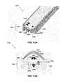
- FIGS. 13A and 13Billustrate another example of an application of a wavelength conversion component in accordance with some embodiments
- FIGS. 14A and 14Billustrate a perspective view and a cross-sectional view of an application of a wavelength conversion component in accordance with some embodiments.
- FIG. 15illustrates a perspective of another application of a wavelength conversion component in accordance with some embodiments.
- photo-luminescent materialembodied specifically as phosphor materials.
- the inventionis applicable to any type of photo-luminescent material, such as either phosphor materials or quantum dots.
- a quantum dotis a portion of matter (e.g. semiconductor) whose excitons are confined in all three spatial dimensions that may be excited by radiation energy to emit light of a particular wavelength or range of wavelengths.
- the inventionis not limited to phosphor based wavelength conversion components unless claimed as such.
- wavelength conversion components for remote wavelength conversionare provided in which a wavelength conversion layer is “sandwiched” between two light transmissive hermetic substrates.
- the light transmissive hermetic substratesform a barrier that protects the wavelength conversion layer from exposure to external environmental conditions.
- the wavelength conversion componentmay further include a sealant material disposed around an outer edge of the sandwich structure, where the sealant material hermetically seals an outer edge wavelength conversion layer.
- the embodiments of the inventionprotects against the degradation of the wavelength conversion layer, since the hermetic substrates and/or sealant material will prevent exposure to external environmental conditions. Moreover, this arrangement also protects against handling damage that may occur to the wavelength conversion layer, such as surface scratches, which also degrades the performance and lifetime of the wavelength conversion layer over time. Additionally, the glass acts as a UV filter, blocking UV light that may potentially damage the wavelength conversion layer.
- the device 100comprises a hollow cylindrical body 101 with a base 103 and sidewalls 105 .
- the device 100further comprises a plurality of blue light emitting LEDs (blue LEDs) 107 that are mounted to the base 105 of the device 100 .
- the LEDs 107may be configured in various arrangements.
- the device 100includes a wavelength conversion component 109 that is operable to absorb a proportion of the blue light generated by the LEDs 107 and convert it to light of a different wavelength by a process of photoluminescence.
- the wavelength conversion component 109is positioned remotely to the LEDs 107 .
- the term “remotely” and “remote”refer to a spaced or separated relationship.
- the wavelength conversion component 109may be positioned a distance of at least 1 cm from the LEDs 107 .
- the wavelength conversion component 109typically comprises a light transmissive substrate 111 and a wavelength conversion layer 113 in contact with the light transmissive substrate 111 .
- the wavelength conversion component 109may be configured such that the wavelength conversion layer 113 is facing the LEDs 107 as illustrated in FIG. 1 .
- the wavelength conversion component 109may be configured such that the light transmissive substrate 111 is facing the LEDs 107 .
- the wavelength conversion layer 113is subject to possible external environmental intrusions.
- FIG. 2illustrates a wavelength conversion component according to some embodiments which protects against such external environmental intrusions.
- the wavelength conversion component 200comprises a first light transmissive hermetic substrate 201 , a second light transmissive hermetic substrate 205 , and a wavelength conversion layer 203 .
- the wavelength conversion layer 203is located between the first light transmissive hermetic substrate 201 and the second light transmissive hermetic substrate 203 .
- the first light transmissive hermetic substrate 201 and the second light transmissive hermetic substrate 205provide a barrier to a first surface of the wavelength conversion layer 203 and a second surface of the wavelength conversion layer 203 .
- the surfaces of the wavelength conversion layer 203may be in direct contact with the light transmissive hermetic substrates 201 , 205 as depicted in FIG. 2 .
- the term “direct contact”means that there are no intervening layers or air gaps. Introducing intervening layers or air gaps at the interface between the wavelength conversion layer 203 and either of the light transmissive hermetic substrates 205 may alter the behavior of light traveling through the wavelength conversion component 200 . As such, creating direct contact at the interface between the wavelength conversion layer 203 and either light transmissive hermetic substrate 201 , 205 may be preferred in order to safeguard against non-ideal behavior of light transmitting through the wavelength conversion component 200 . Furthermore, a light transmissive hermetic substrate 201 , 205 in direct contact with a surface of the wavelength conversion layer 203 creates a barrier against environmental contaminants at that interface.
- the wavelength conversion componentmay be a planar circular disc. In other embodiments, the wavelength conversion component may comprise other geometries such as being convex or concave in form such as for example being dome shaped shell or a cylindrical tube.
- Each light transmissive hermetic substrate 201 , 205must be substantially transmissive to light in the visible spectrum (e.g. 380-740 nm). At such wavelengths, the light transmissive hermetic substrates 201 , 205 should ideally be able to transmit at least 90% of visible light. Each light transmissive hermetic substrate 201 , 205 should also be hermetic.
- the term “hermetic”refers to being substantially impermeable to water, gas, or other environmental contaminants. Examples of light transmissive hermetic substrates include such inorganic materials as glass (e.g., traditional, borosilicate, tempered) and sapphire.
- first light transmissive hermetic substrate 201 and the second light transmissive hermetic substrate 205should have substantially similar indices of refractions in order to ensure proper transmission of light through the wavelength conversion component 200 .
- the first light transmissive hermetic substrate 201 and the second light transmissive hermetic substrate 205may be composed of the same material in order to match indices of refraction as illustrated in FIG. 2 .
- the first light transmissive hermetic substrate 201 and the second light transmissive hermetic substrate 205may be composed of different materials with substantially similar indices of refraction as illustrated in FIG. 4 .
- the first light transmissive hermetic substrate 201 and the second light transmissive hermetic substrate 205should have substantially similar coefficients of thermal expansion. At high temperatures, the wavelength conversion component 200 may experience structural degradation due to mismatched coefficients of thermal expansion of the light transmissive hermetic substrates 201 , 205 . Thus, maintaining substantially similar coefficients of thermal expansion between the light transmissive hermetic substrates 201 , 205 will help preserve the structural integrity of the wavelength conversion component 200 .
- the first light transmissive hermetic substrate 201 and the second light transmissive hermetic substrate 205may be composed of the same material in order to match coefficients of thermal expansion as illustrated in FIG. 2 . In other embodiments, the first light transmissive hermetic substrate 201 and the second light transmissive hermetic substrate 205 may be composed of different materials with substantially similar coefficients of thermal expansion as illustrated in FIG. 4 .
- the wavelength conversion layer 203 of the wavelength conversion component 200comprises a photo-luminescent material.
- the wavelength conversion layer 203may comprise one or more phosphor materials mixed with a carrier material.
- the wavelength conversion layer 203may also include other photo-luminescent material such as quantum dots.
- the carrier materialWhen the wavelength conversion layer 203 comprises a phosphor material mixed with a carrier material, the carrier material must be substantially transmissive to light in the visible spectrum (e.g. 380-740 nm). At such wavelengths, the carrier material should be able to transmit at least 90% of visible light.
- carrier materialsmay include a polymer resin, a monomer resin, an acrylic, an epoxy, a silicone or a fluorinated polymer.
- the carrier materialmay be composed of a U.V. curable material. In some other embodiments, the carrier material may be composed of a thermally curable material.
- the carrier materialshould have an index of refraction that is substantially similar to the indices of refraction of the light transmissive hermetic substrates in order to ensure proper transmission of light through the wavelength conversion component 200 .
- the carrier materialshould have a coefficient of thermal expansion that is substantially similar to the coefficient of thermal expansion of the light transmissive hermetic substrates in order to preserve the structural integrity of the wavelength conversion component 200 .
- the phosphor materialcan comprise an inorganic or organic phosphor such as for example silicate-based phosphor of a general composition A 3 Si(O,D) 5 or A 2 Si(O,D) 4 in which Si is silicon, 0 is oxygen, A comprises strontium (Sr), barium (Ba), magnesium (Mg) or calcium (Ca) and D comprises chlorine (Cl), fluorine (F), nitrogen (N) or sulfur (S).
- silicate-based phosphorsare disclosed in U.S. Pat. No. 7,575,697 B2 “Silicate-based green phosphors”, U.S. Pat. No.
- the phosphorcan also comprise an aluminate-based material such as is taught in co-pending patent application US2006/0158090 A1 “Novel aluminate-based green phosphors” and U.S. Pat. No.
- the phosphor materialis not limited to the examples described and can comprise any phosphor material including nitride and/or sulfate phosphor materials, oxy-nitrides and oxy-sulfate phosphors or garnet materials (YAG).
- the wavelength conversion component 200including the wavelength conversion layer 203 sandwiched between two light transmissive hermetic substrates 201 , 205 provides several advantages.
- the light transmissive hermetic substrates 201 , 205protect the surfaces of the wavelength conversion layer 203 from exposure to environmental contaminants. This limits the potential of such environmental contaminants to potentially initiate a chemical reaction within the wavelength conversion layer 203 that leads to accelerated degradation of that layer.
- the exposure of the wavelength conversion layer to moisturesignificantly increases the potential for accelerated degradation of the phosphor.
- the glassprovides a barrier against exposure to moisture by eliminating the introduction of water into the wavelength conversion layer.
- the path of intrusion for environmental contaminants through the exposed outer edge of the wavelength conversion layer 203is so limited (due to the minimal thickness of the wavelength conversion layer 203 ) that the potential for accelerated degradation of the wavelength conversion layer 203 due to environmental contaminants is minimized.
- a light transmissive hermetic substrate 201 , 205 on each surface of the wavelength conversion layer 203protects against handling damage, such as surface scratches, which also degrade the performance and lifetime of the wavelength conversion layer over time. Furthermore, the light transmissive hermetic substrates 201 , 205 act as a UV filter, thereby blocking UV light that may potentially damage the wavelength conversion layer.
- the wavelength conversion layermay be further hermetically sealed at an outer edge.
- FIG. 3illustrates a wavelength conversion component 300 according to some other embodiments.
- the wavelength conversion component 300 in FIG. 3includes all the features already described above with respect to FIG. 2 . For purposes of discussion, only new features of the wavelength conversion component 300 in FIG. 3 will be discussed.
- the wavelength conversion component 300 in FIG. 3further includes a hermetic sealant material 207 disposed around an outer edge of a sandwich structure formed by the first light transmissive substrate 201 , the wavelength conversion layer 203 , and the second light transmissive substrate 205 .
- the sealant material 207may comprise any material that may be used to form a hermetic seal at the outer edge of the wavelength conversion layer 203 .
- the term “hermetic”refers to being substantially impermeable to water, gas, or other environmental contaminants.
- the sealant material 207forms a protective layer around the outer edge of the wavelength conversion layer 203 , such that the outer edge is impermeable to environmental contaminants.
- glass solder or invare.g., FeNi36 Nickel Steel Alloy with a very low coefficient of thermal expansion
- the sealant material 207should have a substantially similar coefficient of thermal expansion to that of the light transmissive hermetic substrates 201 , 205 and wavelength conversion layer 203 , or a high degree of elasticity.
- a substantially similar coefficient of thermal expansion for the sealant material 207preserves the hermetic seal formed around the outer edge of the wavelength conversion layer 203 for various operating temperatures of the wavelength conversion component 300 .
- a high degree of elasticity of the sealant material 207allows for flexibility at high temperatures such that the hermetic seal formed around the outer edge of the wavelength conversion layer 203 may be preserved.
- the wavelength conversion layer 203may be completely hermetically sealed. Thus, regardless of the dimensions of the wavelength conversion layer 203 , it is protected from environmental contaminants.
- the first light transmissive hermetic substrate 201 and the second light transmissive hermetic substrate 205may be composed of the same material in order to match indices of refraction as illustrated in FIG. 3 .
- the first light transmissive hermetic substrate 201 and the second light transmissive hermetic substrate 205may be composed of different materials with substantially similar indices of refraction as illustrated in FIG. 5A .
- the first light transmissive hermetic substrate 201 and the second light transmissive hermetic substrate 205may be composed of the same material in order to match coefficients of thermal expansion as illustrated in FIG. 3 . In other embodiments, the first light transmissive hermetic substrate 201 and the second light transmissive hermetic substrate 205 may be composed of different materials with substantially similar coefficients of thermal expansion as illustrated in FIG. 5A .
- the outer edge of the wavelength conversion layermay be hermetically sealed using a hermetic holding structure.
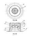
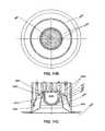
- FIG. 5Billustrates a cross-sectional view of a wavelength conversion component 400 that is hermetically sealed using a hermetic holding structure 209 according to some other embodiments.
- the wavelength conversion component 400 in FIG. 5Bincludes a first light transmissive hermetic substrate 201 , a wavelength conversion layer 203 , and a second light transmissive hermetic substrate 205 as described above in FIG. 2 .
- the wavelength conversion component 400is further disposed within a hermetic holding structure 209 that is in direct contact with an outer edge of the first light transmissive substrate 201 , an outer edge of the wavelength conversion layer 203 , and an outer edge of the second light transmissive substrate 205 .
- each layer of the wavelength conversion component 400could be fabricated within the hermetic holding structure 209 to ensure that the structure 209 forms a hermetic seal around the outer edge of the wavelength conversion component 400 .
- a sealant material 207may be applied to the outer edge of a top surface of the second light transmissive hermetic substrate 207 .
- the sealant material 207need not be applied anywhere else on the wavelength conversion component 400 because the combination of the light transmissive hermetic substrates 201 , 205 and the hermetic sealing structure 209 provides hermetic sealing to protect all other exposed portions of the wavelength conversion layer 203 .
- the sealant material 207should again have a substantially similar coefficient of thermal expansion to that of the light transmissive hermetic substrates 201 , 205 .
- the hermetic holding structure 209can as indicated in FIG. 5B comprise an annular component including base and wall portions, with an optical window to allow light to transmit through the wavelength conversion component 400 . Because light transmitting through the wavelength conversion component 400 need not pass through the hermetic holding structure 209 , the hermetic holding structure 209 can be composed of any material that is hermetic, regardless of its ability to transmit light in the visible range. For example, the hermetic holding structure 209 may be composed of steel, invar (a nickel steel alloy with a low thermal expansion coefficient) or any other opaque material that is hermetic.
- FIG. 6is a flowchart illustrating a method of manufacturing a wavelength conversion component in accordance with some embodiments of the present invention.
- a first light transmissive hermetic substratemay undergo surface preparation as described at 601 .
- Surface preparationmay include steps necessary to remove contaminants prior to deposition of another layer.
- the wavelength conversion layeris then deposited on the first light transmissive hermetic substrate as described at 603 .
- the wavelength conversion layermay be a liquid mixture of phosphor material and carrier material.
- the phosphor materialwhich is in powder form, is thoroughly mixed in known proportions with a liquid light transmissive carrier material to form a suspension.
- the resulting liquid wavelength conversion layeris deposited directly onto the first light transmissive hermetic substrate.
- the wavelength conversion layeris preferably deposited by screen printing though other printing or deposition techniques such as flexograph printing, gravure printing, pad printing, ink jet printing, slot die coating, spin coating, or doctor blading can be used.
- a second light transmissive hermetic substrateis then placed onto the wavelength conversion layer as described at 605 .
- the first light hermetic substrate, the wavelength conversion layer, and the second light transmissive hermetic substratemay then undergo curing as described at 607 .
- Curingallows the liquid wavelength conversion layer to solidify.
- the curing processmay involve U.V. curing. In some other embodiments, the curing process may involve thermal curing.
- a sealant materialmay optionally be deposited along an outer edge of a sandwich structure formed by the first light transmissive substrate, the wavelength conversion layer, and the second light transmissive substrate as described at 609 .
- the sealantforms a hermetic seal along the exposed outer edge of the wavelength conversion layer.
- FIG. 6describes a method for manufacturing a wavelength conversion component in accordance with some embodiments of the invention, additional steps may be taken in the manufacturing process.
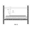
- FIGS. 7A-Dillustrate a method for manufacturing a wavelength conversion component in accordance with some embodiments.
- a first light transmissive hermetic substrate 201may undergo surface preparation and a liquid wavelength conversion layer 203 (e.g., phosphor powder and liquid carrier material) may be deposited thereupon.
- the wavelength conversion layer 203is preferably deposited by screen printing though other deposition techniques such as flexograph printing, gravure printing, pad printing, ink jet printing, slot die coating, spin coating, or doctor blading can be used.
- FIG. 1A first light transmissive hermetic substrate 201 may undergo surface preparation and a liquid wavelength conversion layer 203 (e.g., phosphor powder and liquid carrier material) may be deposited thereupon.
- the wavelength conversion layer 203is preferably deposited by screen printing though other deposition techniques such as flexograph printing, gravure printing, pad printing, ink jet printing, slot die coating, spin coating, or doctor blading can be used.
- FIG. 7Aillustrates a screen printing process, where a layer of photo-luminescent ink 310 is deposited onto a substrate 201 , where a blade 306 (also referred to as a squeegee) is moved in the direction of arrow 332 to spread the ink 310 across a mesh screen 312 to form the material of the wavelength conversion layer 203 .
- the first light transmissive hermetic substrate 201 and the liquid wavelength conversion layer 203may then undergo a curing process to solidify the carrier material.
- the resulting structureis illustrated in FIG. 7B .
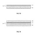
- a thin layer of liquid carrier material 211may then be deposited on top of the wavelength conversion layer 203 , and excess carrier material may be removed using a flexible blade 306 (squeegee).
- the thin layer of liquid carrier materialmay be deposited by flexograph printing, gravure printing, pad printing, ink jet printing, slot die coating, spin coating, or doctor blading can be used.
- the resulting structure after removal of excess carrier materialis illustrated in FIG. 7D .
- the thin layer of liquid carrier material 211is used to ensure proper adhesion of a second light transmissive hermetic substrate.
- the thin layer of liquid carrier material 211does not significantly affect any of the optical or thermal properties of the wavelength conversion layer 203 , and becomes part of the wavelength conversion layer 203 .
- a second light transmissive hermetic substrate 205may undergo surface preparation before being placed on the wavelength conversion layer 203 comprising the thin layer of liquid carrier material 211 .
- the resulting structureis then cured to solidify the thin layer of carrier material 211 .
- the resulting structureis a wavelength conversion component, as illustrated in FIG. 7E .
- FIGS. 8A-Dillustrate views of a method for manufacturing a wavelength conversion component in accordance with some other embodiments.
- a first light transmissive hermetic substrate 201may undergo surface preparation and a liquid wavelength conversion layer 203 (e.g. phosphor material powder and liquid carrier material) may be deposited thereupon.
- the wavelength conversion layer 203is preferably deposited by screen printing though other deposition techniques such as flexograph printing, gravure printing, pad printing, ink jet printing, slot die coating, spin coating, or doctor blading can be used.
- the resulting structureis illustrated in FIG. 8A .
- a second light transmissive hermetic structure 205may then undergo surface preparation before being placed onto the liquid wavelength conversion layer 203 as illustrated in FIG. 8B .
- a lamination processmay be applied as illustrated in FIG. 8C .
- the lamination processmay comprise using rollers 213 to apply uniform pressure across both the first light transmissive hermetic substrate 201 and the second light transmissive hermetic substrate 205 in order to create direct contact between the substrates 201 , 205 and the liquid wavelength conversion layer 203 .
- a final step of curing the first light transmissive hermetic substrate 201 , the second light transmissive hermetic substrate 205 , and liquid wavelength conversion layer 203may be performed to solidify the wavelength conversion layer 203 as illustrated in FIG. 8D .
- wavelength conversion components described abovehave two-dimensional configurations (e.g., generally planar shape), in some other embodiments it is possible for the wavelength conversion component to have a three-dimensional configuration for different applications. This is in contrast to the two-dimensional shape (e.g., generally planar shape) of the wavelength conversion components described above.
- Such three-dimensional componentsmay be useful for applications where it is necessary or desired for light emitted from the light emitting device to be spread over a larger solid angle.
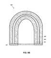
- FIG. 9Aillustrates a wavelength conversion component 900 in accordance with some embodiments.
- the wavelength conversion component 900 of FIG. 9Ais a three-dimensional configuration of the wavelength conversion component 200 of FIG. 2 .
- the wavelength conversion component 900 of FIG. 9Ahas a three-dimensional shape (e.g., elongated dome shaped and/or ellipsoidal shell) whose inner surface defines an interior volume 503 .
- the three-dimensional wavelength conversion component 900 in FIG. 9Aincludes a three-dimensional first light transmissive hermetic substrate 201 ′, a three-dimensional wavelength conversion layer 203 ′, and a three-dimensional second light transmissive hermetic substrate 205 ′ rather than a planar first light transmissive hermetic substrate, a planar wavelength conversion layer, and a planar second light transmissive substrate.
- FIG. 9Billustrates a cross-sectional of a wavelength conversion component 900 ′ in accordance with some embodiments.
- the wavelength conversion component 900 ′ of FIG. 9Bis a three-dimensional configuration of the wavelength conversion component 300 of FIG. 3 .
- the wavelength conversion component 900 ′ of FIG. 9Bhas a three-dimensional shape (e.g., elongated dome shaped and/or ellipsoidal shell).
- the three-dimensional wavelength conversion component 900 ′ in FIG. 9Bincludes a three-dimensional first light transmissive hermetic substrate 201 ′, a three-dimensional wavelength conversion layer 203 ′, and a three-dimensional second light transmissive hermetic substrate 205 ′ rather than a planar first light transmissive substrate, a planar wavelength conversion layer, and a planar second light transmissive substrate.
- 9Bstill includes a hermetic sealant material 207 disposed around an outer edge of a sandwich structure formed by the three-dimensional first light transmissive substrate 201 ′, the three-dimensional wavelength conversion layer 203 ′, and the three-dimensional second light transmissive substrate 205 ′.
- Configuring the wavelength conversion component to be three-dimensional rather than two-dimensionalmay be useful for applications where it is necessary for light emitted from the light emitting device to be spread over a larger volume.
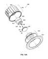
- FIGS. 10A , 10 B, and 10 Cillustrate an example of an application of a wavelength conversion component in accordance with some embodiments.
- FIG. 10A , 10 B, and 10 Cillustrates an LED downlight 1000 that utilizes remote wavelength conversion in accordance with some embodiments.
- FIG. 10Ais an exploded perspective view of the LED downlight 1000
- FIG. 10Bis an end view of the downlight 1000
- FIG. 10Cis a sectional view of the downlight 1000 .
- the downlight 1000is configured to generate light with an emission intensity of 650-700 lumens and a nominal beam spread of 60° (wide flood). It is intended to be used as an energy efficient replacement for a conventional incandescent six inch downlight.
- the downlight 1000comprises a hollow generally cylindrical thermally conductive body 1001 fabricated from, for example, die cast aluminum.
- the body 1001functions as a heat sink and dissipates heat generated by the light emitters 1007 .
- the body 1001can include a series of latitudinal spirally extending heat radiating fins 1003 located towards the base of the body 1001 .
- the outer surface of the bodycan be treated to increase its emissivity such as for example painted black or anodized.
- the body 1001further comprises a generally frustoconical (e.g.
- the form factor of the body 1001is configured to enable the downlight to be retrofitted directly in a standard six inch downlighting fixture (can) as are commonly used in the United States.
- an MCPCBMetal Core Printed Circuit Board
- an MCPCBcomprises a layered structure composed of a metal core base, typically aluminum, a thermally conducting/electrically insulating dielectric layer and a copper circuit layer for electrically connecting electrical components in a desired circuit configuration.
- a thermally conducting compoundsuch as for example a standard heat sink compound containing beryllium oxide or aluminum nitride the metal core base of the MCPCB 1009 is mounted in thermal communication with the body via the floor of the chamber 1005 .
- the MCPCB 1009can be mechanically fixed to the body floor by one or more screws, bolts or other mechanical fasteners.
- the downlight 1000further comprises a hollow generally cylindrical light reflective chamber wall mask 1015 that surrounds the array of light emitters 1007 .
- the chamber wall mask 1015can be made of a plastics material and preferably has a white or other light reflective finish.
- a wavelength conversion component 200such as the one described above in FIG. 2 , may be mounted overlying the front of the chamber wall mask 1015 using, for example, an annular steel clip that has resiliently deformable barbs that engage in corresponding apertures in the body.
- the wavelength conversion component 200may be remote to the light emitters 1007 .
- the wavelength conversion component 200comprises a first light transmissive hermetic substrate 201 , a wavelength conversion layer 203 , and a second light transmissive hermetic substrate 203 as described above.
- the light transmissive hermetic substrates 201 , 205protect the surfaces of the wavelength conversion layer 203 from exposure to environmental contaminants, as discussed above. Additionally, having a light transmissive hermetic substrate 201 , 205 on each surface of the wavelength conversion layer 203 protects against handling damage, such as surface scratches, which also degrade the performance and lifetime of the wavelength conversion layer over time, also discussed above.
- the downlight 1000further comprises a light reflective hood 1025 which is configured to define the selected emission angle (beam spread) of the downlight (e.g. 60° in this example).
- the hood 1025comprises a generally cylindrical shell with three contiguous (conjoint) inner light reflective frustoconical surfaces.
- the hood 1025is preferably made of Acrylonitrile butadiene styrene (ABS) with a metallization layer.
- ABSAcrylonitrile butadiene styrene
- the downlight 1000can comprise an annular trim (bezel) 1027 that can also be fabricated from ABS.
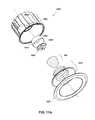
- FIGS. 11A , 11 B, and 11 Cillustrate another example of an application of a wavelength conversion component in accordance with some embodiments.
- FIGS. 11A , 11 B, and 11 Cillustrate an LED downlight 1100 in accordance with some embodiments.
- FIG. 11Ais an exploded perspective view of the LED downlight 1100
- FIG. 11Bis an end view of the downlight 1100
- FIG. 11Cis a sectional view of the downlight 1100 .
- the downlight 1100is configured to generate light with an emission intensity of 650-700 lumens and a nominal beam spread of 60° (wide flood). It is intended to be used as an energy efficient replacement for a conventional incandescent six inch downlight.
- the downlight 1100 of FIGS. 11A , 11 B, and 11 Cis substantially the same as the downlight 1000 of FIGS. 10A , 10 B, and 10 C. For purposes of discussion, only features of the downlight 1100 that are new relative to the embodiments of FIGS. 10A , 10 B, and 10 C will be described.
- the wavelength conversion component 900 of FIGS. 11A , 11 B, and 11 Chas a two-dimensional shape (e.g., is substantially planar)
- the wavelength conversion component 900 of FIGS. 11A , 11 B, and 11 Chas a three-dimensional shape (e.g., elongated dome shaped and/or ellipsoidal shell).
- the three dimensional wavelength conversion component 900includes a three-dimensional first light transmissive hermetic substrate 201 ′, a three-dimensional wavelength conversion layer 203 ′, and a three-dimensional second light transmissive hermetic substrate 205 ′, such as the wavelength conversion component 900 described above in FIG. 9A .
- the wavelength conversion componentmay also be mounted enclosing the front of the chamber wall mask 1015 .
- the light transmissive hermetic substrates 201 ′, 205 ′protect the surfaces of the wavelength conversion layer 203 ′ from exposure to environmental contaminants, as discussed above. Additionally, having a light transmissive hermetic substrate 201 ′, 205 ′ on each surface of the wavelength conversion layer 203 ′ protects against handling damage, such as surface scratches, which also degrade the performance and lifetime of the wavelength conversion layer over time.
- FIG. 12illustrates another example of an application of a wavelength conversion component in accordance with some embodiments.
- FIG. 12illustrates an exploded perspective view of a reflector lamp 1200 in accordance with some embodiments.
- the reflector lamp 1200is configured to generate light with an emission intensity of 650-700 lumens and a nominal beam spread of 60° (wide flood). It is intended to be used as an energy efficient replacement for a conventional incandescent six inch downlight.
- the reflector lamp 1200comprises a generally rectangular thermally conductive body 1201 fabricated from, for example, die cast aluminum.
- the body 1201functions as a heat sink and dissipates heat generated by the light emitting device 1203 .
- the body 1201can include a series of heat radiating fins 1207 located on the sides of the body 1201 .
- the outer surface of the body 1201can be treated to increase its emissivity such as for example painted black or anodized.
- the body 1201further comprises a thermally conductive pad that may be placed in contact with a thermally conductive base of the light emitting device 1203 .
- the form factor of the body 1201is configured to enable the downlight to be retrofitted directly in a standard six inch downlighting fixture (a “can”) as are commonly used in the United States.
- a light emitting device 1203 that includes a wavelength conversion component 200 such as the one described above with respect to FIG. 2may be attached to the body 1201 such that the thermally conductive base of the light emitting device 1203 may be in thermal contact with the thermally conductive pad of the body 1201 .
- the light emitting device 1203may include a hollow cylindrical body with a base and sidewalls that is substantially the same as the cylindrical body described in FIG. 1 that is configured to house the wavelength conversion component 200 .
- the wavelength conversion component 200may include a first light transmissive hermetic substrate, a wavelength conversion layer, and a second light transmissive hermetic substrate, as described above with respect to FIG. 2 .
- the light transmissive hermetic substratesprotect the surfaces of the wavelength conversion layer from exposure to environmental contaminants, as discussed above. Additionally, having a light transmissive hermetic substrate on each surface of the wavelength conversion layer protects against handling damage, such as surface scratches, which also degrade the performance and lifetime of the wavelength conversion layer over time.
- the reflector lamp 1200further comprises a generally frustroconical light reflector 1205 having a paraboloidal light reflective inner surface which is configured to define the selected emission angle (beam spread) of the downlight (e.g. 60° in this example).
- the reflector 1205is preferably made of Acrylonitrile butadiene styrene (ABS) with a metallization layer.
- ABSAcrylonitrile butadiene styrene
- FIGS. 13A and 13Billustrate another example of an application of a wavelength conversion component in accordance with some embodiments.
- FIGS. 13A and 13Billustrate an LED linear lamp 1300 in accordance with some embodiments.
- FIG. 13Ais a three-dimensional perspective view of the linear lamp 1300 and
- FIG. 13Bis a cross-sectional view of the linear lamp 1300 .
- the LED linear lamp 1300is intended to be used as an energy efficient replacement for a conventional incandescent or fluourescent tube lamp.
- the linear lamp 1300comprises an elongated thermally conductive body 1301 fabricated from, for example, die cast aluminum.
- the form factor of the body 1301is configured to be mounted with a standard linear lamp housing.
- the body 1301further comprises a first recessed channel 1304 , wherein a rectangular tube-like case 1307 containing some electrical components (e.g., electrical wires) of the linear lamp 1300 may be situated.
- the case 1307may further comprise an electrical connector 1309 (e.g., plug) extending past the length of the body 1301 on one end, and a recessed complimentary socket (not shown) configured to receive a connector on another end.
- the body 1301functions as a heat sink and dissipates heat generated by the light emitters 1303 .
- the body 1301can include a series of heat radiating fins 1302 located on the sides of the body 1301 .
- the outer surface of the body 1301can be treated to increase its emissivity such as for example painted black or anodized.
- Light emitters 1303are mounted on a strip (rectangular shaped) MCPCB 1305 configured to sit above the first recessed channel 1304 .
- the under surface of the MCPCB 1305sits in thermal contact with a second recessed channel 1306 that includes inclined walls 1308 .
- a generally hemi-spherical elongate wavelength conversion component 1311may be positioned remote to the light emitters 1303 .
- the wavelength conversion component 1311may be secured within the second recessed channel 1306 by sliding the wavelength conversion component 1311 under the inclined walls 1308 such that the wavelength conversion component 1311 engages with inclined walls 1308 .
- the wavelength conversion component 1311may also be flexibly placed under the inclined walls 1308 such that the wavelength conversion component 1311 engages with the inclined walls 1308 .
- the wavelength conversion component 1311may include a hemi-spherical elongate first light transmissive hermetic substrate 1313 , a hemi-spherical elongate wavelength conversion layer 1315 , and a hemi-spherical elongate second light transmissive hermetic substrate 1317 .
- the light transmissive hermetic substrates 1313 , 1317protect the surfaces of the wavelength conversion layer 1315 from exposure to environmental contaminants, as discussed above. Additionally, having a light transmissive hermetic substrate 1313 , 1317 on each surface of the wavelength conversion layer 1315 protects against handling damage, such as surface scratches, which also degrade the performance and lifetime of the wavelength conversion layer 1315 over time.
- the wavelength conversion component of the linear lampmay be configured in the shape of a generally planar strip.
- the second recessed channelmay instead have vertical walls that extend to allow the wavelength conversion component to be received by the second recessed channel.
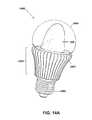
- FIGS. 14A and 14Billustrate a perspective view and a cross-sectional view of an application of a wavelength conversion component in accordance with some embodiments.
- FIGS. 14A and 14Billustrate an LED light bulb 1400 that utilizes remote wavelength conversion.
- the LED light bulb 1400is intended to be used as an energy efficient replacement for a conventional incandescent or fluorescent light bulb.
- the light bulb 1400comprises a screw base 1401 that is configured to fit within standard light bulb sockets, e.g. implemented as a standard Edison screw base.
- the light bulb 1400may further comprise a thermally conductive body 1403 fabricated from, for example, die cast aluminum.
- the body 1403functions as a heat sink and dissipates heat generated by the light emitters 1409 , which are mounted on a MCPCB 1405 .
- the MCPCB 1405may be in thermal contact with the body 1403 .
- the body 1403can include a series of latitudinal radially extending heat radiating fins 1407 .
- the outer surface of the body 1403can be treated to increase its emissivity such as for example painted black or anodized.
- the light bulb 1400comprises a wavelength conversion component 900 , such as the one described above in FIG. 9 , having a three-dimensional shape (e.g., elongated dome shaped and/or ellipsoidal shell) that encloses the light emitters 1409 .
- the three dimensional wavelength conversion component 900includes a three-dimensional first light transmissive hermetic substrate 201 ′, a three-dimensional wavelength conversion layer 203 ′, and a three-dimensional second light transmissive hermetic substrate 205 ′.
- the light transmissive hermetic substrates 201 ′, 205 ′protect the surfaces of the wavelength conversion layer 203 ′ from exposure to environmental contaminants, as discussed above.
- wavelength conversion layer 203 ′protects against handling damage, such as surface scratches, which also degrade the performance and lifetime of the wavelength conversion layer 203 ′ over time.
- An envelope 1411may extend around the upper portion of the LED light bulb 1400 , enclosing the light emitters 1409 and the wavelength conversion component 900 .
- the envelope 1411is a light-transmissive material (e.g. glass or plastic) that provides protective and/or diffusive properties for the LED light bulb 1400 .
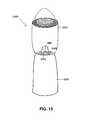
- FIG. 15illustrates a perspective of another application of a wavelength conversion component in accordance with some embodiments.
- FIG. 15illustrates an LED lantern 1500 that utilizes remote wavelength conversion.
- the LED light lantern 1500is intended to be used as an energy efficient replacement for conventional gas and fluorescent lanterns (e.g., camping lanterns).
- the lantern 1500comprises a generally cylindrical thermally conductive body 1501 fabricated from, for example, plastic material or pressed metal.
- the body 1501further includes an internal heat sink which dissipates heat generated by the light emitters 1503 , which are mounted on a circular shaped MCPCB 1505 .
- the MCPCB 1505may be in thermal contact with the body 1501 .
- the lantern 1500comprises a three-dimensional (e.g., elongated dome shaped and/or ellipsoidal shell) wavelength conversion component 900 , such as the one described above in FIG. 9 , that extends from the MCPCB 1505 . While only an exterior surface of the wavelength conversion component 900 is depicted, it is important to note that the three dimensional wavelength conversion component 900 may include a three-dimensional first light transmissive hermetic substrate, a three-dimensional wavelength conversion layer, and a three-dimensional second light transmissive hermetic substrate, as described in FIG. 9 .
- a three-dimensional wavelength conversion component 900may include a three-dimensional first light transmissive hermetic substrate, a three-dimensional wavelength conversion layer, and a three-dimensional second light transmissive hermetic substrate, as described in FIG. 9 .
- the light transmissive hermetic substratesprotect the surfaces of the wavelength conversion layer from exposure to environmental contaminants. Additionally, having a light transmissive hermetic substrate on each surface of the wavelength conversion layer protects against handling damage, such as surface scratches, which also degrade the performance and lifetime of the wavelength conversion layer over time.
- a light transmissive cover 1507may extend around the upper portion of the lantern, surrounding the light emitters 1503 and the wavelength conversion component 900 .
- the light transmissive cover 1507comprises a light-transmissive material (e.g. glass or plastic) that provides protective and/or diffusive properties for the LED lantern 1500 .
- the lantern 1500may further comprise a lid that sits on top of the light transmissive cover 1507 to enclose the light emitters 1503 and the wavelength conversion component 900 .
- the above applications of light emitting devicesdescribe a remote wavelength conversion configuration, wherein a wavelength conversion component is remote to one or more light emitters.
- the wavelength conversion component and body of those light emitting devicesdefine an interior volume wherein the light emitters are located.
- the interior volumemay also be referred to as a light mixing chamber.
- an interior volume 1029is defined by the wavelength conversion component 200 , 900 , the light reflective chamber mask 1015 , and the body of the downlight 1001 .
- an interior volume 1325is defined by the wavelength conversion component 1311 and the body of the linear lamp 1301 .
- an interior volume 1415is defined by the wavelength conversion component 900 and the body of the light bulb 1407 .
- Such an interior volumeprovides a physical separation (air gap) of the wavelength conversion component from the light emitters that improves the thermal characteristics of the light emitting device. Due to the isotropic nature of photoluminescence light generation, approximately half of the light generated by the phosphor material can be emitted in a direction towards the light emitters and can end up in the light mixing chamber. It is believed that on average as little as 1 in a 10,000 interactions of a photon with a phosphor material particle results in absorption and generation of photoluminescence light.
- the majority, about 99.99%, of interactions of photons with a phosphor particleresult in scattering of the photon. Due to the isotropic nature of the scattering process on average half the scattered photons will be in a direction back towards the light emitters. As a result up to half of the light generated by the light emitters that is not absorbed by the phosphor material can also end up back in the light mixing chamber.
- the interior volume of the mixing chamberincludes light reflective surfaces to redirect—light in—the interior volume towards the wavelength conversion component and out of the device.
- the light mixing chambermay also operate to mix light within the chamber.
- the light mixing chambercan be defined by the wavelength conversion component in conjunction with another component of the device such a device body or housing (e.g., dome-shaped wavelength conversion component encloses light emitters located on a base of device body to define light mixing chamber, or planar wavelength conversion component placed on a chamber shaped component to enclose light emitters located on a base of device body and surrounded by the chamber shaped component to define light mixing chamber).
- a device body or housinge.g., dome-shaped wavelength conversion component encloses light emitters located on a base of device body to define light mixing chamber, or planar wavelength conversion component placed on a chamber shaped component to enclose light emitters located on a base of device body and surrounded by the chamber shaped component to define light mixing chamber.
- the linear lamp 1300 of FIGS. 11A and 11Bincludes an MCPCB 1305 , on which the light emitters 1303 are mounted, comprising light reflective material to facilitate the redirection of light reflected back into the interior volume towards the wavelength conversion component 1311 .
- the light bulb 1400 of FIGS. 12A and 12Balso includes an MCPCB 1405 , on which the light emitters 1409 are mounted, to facilitate the redirection of light reflected back into the interior volume towards the wavelength conversion component 900 .
- the improved wavelength conversion componentcomprises a wavelength conversion layer between a first light transmissive hermetic substrate and a second light transmissive hermetic substrate.
Landscapes
- Physics & Mathematics (AREA)
- Spectroscopy & Molecular Physics (AREA)
- Engineering & Computer Science (AREA)
- General Engineering & Computer Science (AREA)
- Led Device Packages (AREA)
- Optical Filters (AREA)
Abstract
Description
Claims (13)
Priority Applications (3)
| Application Number | Priority Date | Filing Date | Title |
|---|---|---|---|
| US13/273,196US9115868B2 (en) | 2011-10-13 | 2011-10-13 | Wavelength conversion component with improved protective characteristics for remote wavelength conversion |
| TW101137079ATW201319467A (en) | 2011-10-13 | 2012-10-08 | Wavelength conversion component with improved protective characteristics for remote wavelength conversion |
| PCT/US2012/059505WO2013055764A1 (en) | 2011-10-13 | 2012-10-10 | Wavelength conversion component with improved protective characteristics for remote wavelength conversion |
Applications Claiming Priority (1)
| Application Number | Priority Date | Filing Date | Title |
|---|---|---|---|
| US13/273,196US9115868B2 (en) | 2011-10-13 | 2011-10-13 | Wavelength conversion component with improved protective characteristics for remote wavelength conversion |
Publications (2)
| Publication Number | Publication Date |
|---|---|
| US20130094176A1 US20130094176A1 (en) | 2013-04-18 |
| US9115868B2true US9115868B2 (en) | 2015-08-25 |
Family
ID=48082379
Family Applications (1)
| Application Number | Title | Priority Date | Filing Date |
|---|---|---|---|
| US13/273,196Expired - Fee RelatedUS9115868B2 (en) | 2011-10-13 | 2011-10-13 | Wavelength conversion component with improved protective characteristics for remote wavelength conversion |
Country Status (3)
| Country | Link |
|---|---|
| US (1) | US9115868B2 (en) |
| TW (1) | TW201319467A (en) |
| WO (1) | WO2013055764A1 (en) |
Families Citing this family (20)
| Publication number | Priority date | Publication date | Assignee | Title |
|---|---|---|---|---|
| US8908261B2 (en)* | 2011-01-26 | 2014-12-09 | Massachusetts Institute Of Technology | Device and method for luminescence enhancement by resonant energy transfer from an absorptive thin film |
| US20130187534A1 (en)* | 2012-01-20 | 2013-07-25 | Remphos Technologies Llc | Phosphorized kernels for remote phosphor led |
| KR20140077408A (en)* | 2012-12-14 | 2014-06-24 | 엘지전자 주식회사 | Method for manufacturing phosphor film and the phosphor film manufactured by the same |
| TWI510741B (en)* | 2013-05-27 | 2015-12-01 | Genesis Photonics Inc | Illuminating device |
| US9316388B2 (en)* | 2014-01-31 | 2016-04-19 | Christie Digital Systems Usa, Inc. | Device and kit for cooling a light emitting material |
| CN105981186A (en)* | 2014-02-11 | 2016-09-28 | 飞利浦照明控股有限公司 | Wavelength conversion element, light emitting module and lamp |
| EP3117267B1 (en)* | 2014-03-11 | 2018-05-02 | Osram Sylvania Inc. | Light converter assemblies with enhanced heat dissipation |
| KR101555954B1 (en)* | 2014-04-01 | 2015-09-30 | 코닝정밀소재 주식회사 | Substrate for color conversion of led and method of fabricating threof |
| KR101549407B1 (en)* | 2014-04-17 | 2015-09-03 | 코닝정밀소재 주식회사 | Substrate for color conversion of led and method of fabricating threof |
| CN105101606A (en)* | 2014-04-24 | 2015-11-25 | 鸿富锦精密工业(深圳)有限公司 | Three-dimensional circuit board and light-emitting diode lamp with the three-dimensional circuit board |
| JP2016004954A (en)* | 2014-06-18 | 2016-01-12 | 日本電気硝子株式会社 | Light emitting device, wavelength conversion member, and method of manufacturing wavelength conversion member |
| JP2016076634A (en)* | 2014-10-08 | 2016-05-12 | エルジー ディスプレイ カンパニー リミテッド | Led package, backlight unit, and liquid crystal display device |
| JP6448365B2 (en)* | 2014-12-26 | 2019-01-09 | シチズン時計株式会社 | Light emitting device and projection device |
| CN104633496B (en)* | 2014-12-31 | 2017-07-18 | 东莞凯裕光电科技有限公司 | Bulb production equipment and production method |
| US9869464B2 (en)* | 2015-09-23 | 2018-01-16 | Cooper Technologies Company | Hermetically-sealed light fixture for hazardous environments |
| US10244599B1 (en) | 2016-11-10 | 2019-03-26 | Kichler Lighting Llc | Warm dim circuit for use with LED lighting fixtures |
| FR3061404B1 (en)* | 2016-12-27 | 2022-09-23 | Packaging Sip | METHOD FOR THE COLLECTIVE MANUFACTURING OF HERMETIC ELECTRONIC MODULES |
| JP7071616B2 (en)* | 2017-09-29 | 2022-05-19 | 日亜化学工業株式会社 | Light source device |
| CN110176529B (en)* | 2018-02-20 | 2022-03-08 | 晶元光电股份有限公司 | Light-emitting element and method of making the same |
| JP6768093B2 (en)* | 2019-01-11 | 2020-10-14 | エルジー ディスプレイ カンパニー リミテッド | LED package, backlight unit and liquid crystal display device |
Citations (154)
| Publication number | Priority date | Publication date | Assignee | Title |
|---|---|---|---|---|
| US3290255A (en) | 1963-09-30 | 1966-12-06 | Gen Electric | White electroluminescent phosphor |
| US3593055A (en) | 1969-04-16 | 1971-07-13 | Bell Telephone Labor Inc | Electro-luminescent device |
| US3670193A (en) | 1970-05-14 | 1972-06-13 | Duro Test Corp | Electric lamps producing energy in the visible and ultra-violet ranges |
| US3676668A (en) | 1969-12-29 | 1972-07-11 | Gen Electric | Solid state lamp assembly |
| US3691482A (en) | 1970-01-19 | 1972-09-12 | Bell Telephone Labor Inc | Display system |
| US3709685A (en) | 1970-02-19 | 1973-01-09 | Ilford Ltd | Photoconductive zinc oxide sensitized by substituted thiazolidene dyes |
| JPS4820539U (en) | 1971-07-16 | 1973-03-08 | ||
| US3743833A (en) | 1971-07-16 | 1973-07-03 | Eastman Kodak Co | Radiographic elements and binders |
| US3763405A (en) | 1970-12-21 | 1973-10-02 | Nippon Electric Co | Solid state luminescent display device |
| US3793046A (en) | 1970-12-04 | 1974-02-19 | Philips Corp | Method of manufacturing a pigment |
| US3819974A (en) | 1973-03-12 | 1974-06-25 | D Stevenson | Gallium nitride metal-semiconductor junction light emitting diode |
| US3819973A (en) | 1972-11-02 | 1974-06-25 | A Hosford | Electroluminescent filament |
| US3849707A (en) | 1973-03-07 | 1974-11-19 | Ibm | PLANAR GaN ELECTROLUMINESCENT DEVICE |
| US3875456A (en) | 1972-04-04 | 1975-04-01 | Hitachi Ltd | Multi-color semiconductor lamp |
| JPS5079379U (en) | 1973-11-24 | 1975-07-09 | ||
| US3932881A (en) | 1972-09-05 | 1976-01-13 | Nippon Electric Co., Inc. | Electroluminescent device including dichroic and infrared reflecting components |
| US3937998A (en) | 1973-10-05 | 1976-02-10 | U.S. Philips Corporation | Luminescent coating for low-pressure mercury vapour discharge lamp |
| US3972717A (en) | 1973-03-21 | 1976-08-03 | Hoechst Aktiengesellschaft | Electrophotographic recording material |
| US4047075A (en) | 1975-03-01 | 1977-09-06 | Licentia-Patent-Verwaltungs-G.M.B.H. | Encapsulated light-emitting diode structure and array thereof |
| US4081764A (en) | 1972-10-12 | 1978-03-28 | Minnesota Mining And Manufacturing Company | Zinc oxide light emitting diode |
| US4104076A (en) | 1970-03-17 | 1978-08-01 | Saint-Gobain Industries | Manufacture of novel grey and bronze glasses |
| US4143394A (en) | 1976-07-30 | 1979-03-06 | Licentia Patent-Verwaltungs-G.M.B.H. | Semiconductor luminescence device with housing |
| GB2017409A (en) | 1978-03-22 | 1979-10-03 | Bayraktaroglu B | Light-emitting diode |
| US4176294A (en) | 1975-10-03 | 1979-11-27 | Westinghouse Electric Corp. | Method and device for efficiently generating white light with good rendition of illuminated objects |
| US4176299A (en) | 1975-10-03 | 1979-11-27 | Westinghouse Electric Corp. | Method for efficiently generating white light with good color rendition of illuminated objects |
| US4211955A (en) | 1978-03-02 | 1980-07-08 | Ray Stephen W | Solid state lamp |
| US4305019A (en) | 1979-12-31 | 1981-12-08 | Westinghouse Electric Corp. | Warm-white fluorescent lamp having good efficacy and color rendering and using special phosphor blend as separate undercoat |
| US4315192A (en) | 1979-12-31 | 1982-02-09 | Westinghouse Electric Corp. | Fluorescent lamp using high performance phosphor blend which is protected from color shifts by a very thin overcoat of stable phosphor of similar chromaticity |
| US4443532A (en) | 1981-07-29 | 1984-04-17 | Bell Telephone Laboratories, Incorporated | Induced crystallographic modification of aromatic compounds |
| JPS60170194U (en) | 1984-04-20 | 1985-11-11 | 鈴木 悦三 | Roll paper holder that can be opened and closed |
| US4559470A (en) | 1981-04-22 | 1985-12-17 | Mitsubishi Denki Kabushiki Kaisha | Fluorescent discharge lamp |
| US4573766A (en) | 1983-12-19 | 1986-03-04 | Cordis Corporation | LED Staggered back lighting panel for LCD module |
| US4618555A (en) | 1984-01-11 | 1986-10-21 | Mitsubishi Chemical Ind., Ltd. | Electrophotographic photoreceptor comprising azo compounds |
| US4638214A (en) | 1985-03-25 | 1987-01-20 | General Electric Company | Fluorescent lamp containing aluminate phosphor |
| US4667036A (en) | 1983-08-27 | 1987-05-19 | Basf Aktiengesellschaft | Concentration of light over a particular area, and novel perylene-3,4,9,10-tetracarboxylic acid diimides |
| US4678285A (en) | 1984-01-13 | 1987-07-07 | Ricoh Company, Ltd. | Liquid crystal color display device |
| US4727003A (en) | 1985-09-30 | 1988-02-23 | Ricoh Company, Ltd. | Electroluminescence device |
| US4772885A (en) | 1984-11-22 | 1988-09-20 | Ricoh Company, Ltd. | Liquid crystal color display device |
| US4845223A (en) | 1985-12-19 | 1989-07-04 | Basf Aktiengesellschaft | Fluorescent aryloxy-substituted perylene-3,4,9,10-tetracarboxylic acid diimides |
| JPH01179471A (en) | 1988-01-07 | 1989-07-17 | Natl Inst For Res In Inorg Mater | Cubic boron nitride P-n junction light emitting device |
| US4859539A (en) | 1987-03-23 | 1989-08-22 | Eastman Kodak Company | Optically brightened polyolefin coated paper support |
| JPH01260707A (en) | 1988-04-11 | 1989-10-18 | Idec Izumi Corp | Device for emitting white light |
| JPH0291980A (en) | 1988-09-29 | 1990-03-30 | Toshiba Lighting & Technol Corp | solid state light emitting device |
| US4915478A (en) | 1988-10-05 | 1990-04-10 | The United States Of America As Represented By The Secretary Of The Navy | Low power liquid crystal display backlight |
| US4918497A (en) | 1988-12-14 | 1990-04-17 | Cree Research, Inc. | Blue light emitting diode formed in silicon carbide |
| US4946621A (en) | 1986-04-29 | 1990-08-07 | Centre National De La Recherche Scientifique (Cnrs) | Luminescent mixed borates based on rare earths |
| US4992704A (en) | 1989-04-17 | 1991-02-12 | Basic Electronics, Inc. | Variable color light emitting diode |
| JPH0324692B2 (en) | 1982-10-07 | 1991-04-03 | Hideo Itokawa | |
| WO1991008508A1 (en) | 1989-11-24 | 1991-06-13 | Innovare Limited | A display device |
| US5077161A (en) | 1990-05-31 | 1991-12-31 | Xerox Corporation | Imaging members with bichromophoric bisazo perylene photoconductive materials |
| US5110931A (en) | 1987-11-27 | 1992-05-05 | Hoechst Aktiengesellschaft | Process for the preparation of n,n'-dimethylperylene-3,4,9,10-tetracarboxylic diimide in high-hiding pigment form |
| US5126214A (en) | 1989-03-15 | 1992-06-30 | Idemitsu Kosan Co., Ltd. | Electroluminescent element |
| US5131916A (en) | 1990-03-01 | 1992-07-21 | Bayer Aktiengesellschaft | Colored fluorescent polymer emulsions for marker pens: graft copolymers and fluorescent dyes in aqueous phase |
| US5143438A (en) | 1990-10-15 | 1992-09-01 | Thorn Emi Plc | Light sources |
| US5143433A (en) | 1991-11-01 | 1992-09-01 | Litton Systems Canada Limited | Night vision backlighting system for liquid crystal displays |
| JPH04269718A (en) | 1991-02-25 | 1992-09-25 | Shimadzu Corp | LCD display with backlight |
| JPH04289691A (en) | 1990-12-07 | 1992-10-14 | Mitsubishi Cable Ind Ltd | El illuminant |
| JPH04321280A (en) | 1991-04-19 | 1992-11-11 | Nichia Chem Ind Ltd | Blue color light-emitting diode |
| US5166761A (en) | 1991-04-01 | 1992-11-24 | Midwest Research Institute | Tunnel junction multiple wavelength light-emitting diodes |
| US5208462A (en) | 1991-12-19 | 1993-05-04 | Allied-Signal Inc. | Wide bandwidth solid state optical source |
| US5210051A (en) | 1990-03-27 | 1993-05-11 | Cree Research, Inc. | High efficiency light emitting diodes from bipolar gallium nitride |
| US5211467A (en) | 1992-01-07 | 1993-05-18 | Rockwell International Corporation | Fluorescent lighting system |
| JPH05152609A (en) | 1991-11-25 | 1993-06-18 | Nichia Chem Ind Ltd | Light emitting diode |
| US5237182A (en) | 1990-11-29 | 1993-08-17 | Sharp Kabushiki Kaisha | Electroluminescent device of compound semiconductor with buffer layer |
| US5264034A (en) | 1989-08-11 | 1993-11-23 | Hoechst Aktiengesellschaft | Pigment preparations based on perylene compounds |
| US5283425A (en) | 1992-02-06 | 1994-02-01 | Rohm Co., Ltd. | Light emitting element array substrate with reflecting means |
| WO1994000973A3 (en) | 1992-11-06 | 1994-04-14 | Josef Dirr | Information coding and transmission process |
| EP0395775B1 (en) | 1989-05-02 | 1994-08-03 | Nichia Kagaku Kogyo K.K. | Phosphor composition used for fluorescent lamp and fluorescent lamp using the same |
| JPH06267301A (en) | 1993-03-15 | 1994-09-22 | Olympus Optical Co Ltd | Organic photoluminescence element |
| US5369289A (en) | 1991-10-30 | 1994-11-29 | Toyoda Gosei Co. Ltd. | Gallium nitride-based compound semiconductor light-emitting device and method for making the same |
| US5405709A (en) | 1993-09-13 | 1995-04-11 | Eastman Kodak Company | White light emitting internal junction organic electroluminescent device |
| JPH07176794A (en) | 1993-12-17 | 1995-07-14 | Nichia Chem Ind Ltd | Surface light source |
| US5439971A (en) | 1991-11-12 | 1995-08-08 | Eastman Chemical Company | Fluorescent pigment concentrates |
| JPH07235207A (en) | 1994-02-21 | 1995-09-05 | Copal Co Ltd | Back light |
| JPH0799345B2 (en) | 1988-10-31 | 1995-10-25 | 防衛庁技術研究本部長 | Method and apparatus for generating water temperature profile data |
| JPH07282609A (en) | 1994-04-06 | 1995-10-27 | Tsuzuki Shogo | Light source device for illumination using semiconductor laser device |
| JPH087614B2 (en) | 1992-03-27 | 1996-01-29 | 株式会社牧野フライス製作所 | Method and device for correcting tool length of machine tool |
| US5518808A (en) | 1992-12-18 | 1996-05-21 | E. I. Du Pont De Nemours And Company | Luminescent materials prepared by coating luminescent compositions onto substrate particles |
| US5557168A (en) | 1993-04-02 | 1996-09-17 | Okaya Electric Industries Co., Ltd. | Gas-discharging type display device and a method of manufacturing |
| JPH08250281A (en) | 1995-03-08 | 1996-09-27 | Olympus Optical Co Ltd | Luminescent element and displaying apparatus |
| US5563621A (en) | 1991-11-18 | 1996-10-08 | Black Box Vision Limited | Display apparatus |
| US5578839A (en) | 1992-11-20 | 1996-11-26 | Nichia Chemical Industries, Ltd. | Light-emitting gallium nitride-based compound semiconductor device |
| US5583349A (en) | 1995-11-02 | 1996-12-10 | Motorola | Full color light emitting diode display |
| US5585640A (en) | 1995-01-11 | 1996-12-17 | Huston; Alan L. | Glass matrix doped with activated luminescent nanocrystalline particles |
| US5619356A (en) | 1993-09-16 | 1997-04-08 | Sharp Kabushiki Kaisha | Reflective liquid crystal display device having a compensator with a retardation value between 0.15 μm and 0.38 μm and a single polarizer |
| EP0534140B1 (en) | 1991-08-22 | 1997-07-16 | Tosoh Corporation | Backlighting device |
| US5660461A (en) | 1994-12-08 | 1997-08-26 | Quantum Devices, Inc. | Arrays of optoelectronic devices and method of making same |
| US5677417A (en) | 1993-05-04 | 1997-10-14 | Max-Planck-Gesellschaft Zur Foerderung | Tetraaroxyperylene-3,4,9,10-tetracarboxylic polyimides |
| US5679152A (en) | 1994-01-27 | 1997-10-21 | Advanced Technology Materials, Inc. | Method of making a single crystals Ga*N article |
| US5763901A (en) | 1992-12-17 | 1998-06-09 | Kabushiki Kaisha Toshiba | Semiconductor light-emitting device and method for manufacturing the device |
| US5770887A (en) | 1993-10-08 | 1998-06-23 | Mitsubishi Cable Industries, Ltd. | GaN single crystal |
| US5771039A (en) | 1994-06-06 | 1998-06-23 | Ditzik; Richard J. | Direct view display device integration techniques |
| US5777350A (en) | 1994-12-02 | 1998-07-07 | Nichia Chemical Industries, Ltd. | Nitride semiconductor light-emitting device |
| US5869199A (en) | 1993-03-26 | 1999-02-09 | Sumitomo Electric Industries, Ltd. | Organic electroluminescent elements comprising triazoles |
| JP2900928B2 (en) | 1997-10-20 | 1999-06-02 | 日亜化学工業株式会社 | Light emitting diode |
| US5959316A (en) | 1998-09-01 | 1999-09-28 | Hewlett-Packard Company | Multiple encapsulation of phosphor-LED devices |
| US5962971A (en) | 1997-08-29 | 1999-10-05 | Chen; Hsing | LED structure with ultraviolet-light emission chip and multilayered resins to generate various colored lights |
| US5998925A (en) | 1996-07-29 | 1999-12-07 | Nichia Kagaku Kogyo Kabushiki Kaisha | Light emitting device having a nitride compound semiconductor and a phosphor containing a garnet fluorescent material |
| US6137217A (en) | 1992-08-28 | 2000-10-24 | Gte Products Corporation | Fluorescent lamp with improved phosphor blend |
| US6340824B1 (en) | 1997-09-01 | 2002-01-22 | Kabushiki Kaisha Toshiba | Semiconductor light emitting device including a fluorescent material |
| US6504301B1 (en) | 1999-09-03 | 2003-01-07 | Lumileds Lighting, U.S., Llc | Non-incandescent lightbulb package using light emitting diodes |
| US6576488B2 (en) | 2001-06-11 | 2003-06-10 | Lumileds Lighting U.S., Llc | Using electrophoresis to produce a conformally coated phosphor-converted light emitting semiconductor |
| US6600175B1 (en) | 1996-03-26 | 2003-07-29 | Advanced Technology Materials, Inc. | Solid state white light emitter and display using same |
| JP2003234513A (en) | 2003-02-04 | 2003-08-22 | Nichia Chem Ind Ltd | Resin for wavelength conversion light emitting diode to which fluorescent dye or fluorescent pigment is added |
| US6642618B2 (en) | 2000-12-21 | 2003-11-04 | Lumileds Lighting U.S., Llc | Light-emitting device and production thereof |
| US6642652B2 (en) | 2001-06-11 | 2003-11-04 | Lumileds Lighting U.S., Llc | Phosphor-converted light emitting device |
| JP2004071771A (en) | 2002-08-05 | 2004-03-04 | Okaya Electric Ind Co Ltd | Light emitting diode |
| US6759809B2 (en)* | 2002-07-19 | 2004-07-06 | Gary M. Grant | Illuminated graphics system |
| WO2004021461A3 (en) | 2002-08-30 | 2004-09-30 | Gelcore Llc | Phosphor-coated led with improved efficiency |
| US20040227149A1 (en) | 2003-04-30 | 2004-11-18 | Cree, Inc. | High powered light emitter packages with compact optics |
| US6869812B1 (en) | 2003-05-13 | 2005-03-22 | Heng Liu | High power AllnGaN based multi-chip light emitting diode |
| US20050152146A1 (en) | 2002-05-08 | 2005-07-14 | Owen Mark D. | High efficiency solid-state light source and methods of use and manufacture |
| WO2005106926A2 (en) | 2004-04-26 | 2005-11-10 | Gelcore Llc | Light emitting diode component |
| JP3724490B2 (en) | 2004-01-19 | 2005-12-07 | 日亜化学工業株式会社 | Light emitting diode |
| US20060060867A1 (en) | 2004-09-09 | 2006-03-23 | Toyoda Gosei Co., Ltd. | Light emitting device |
| JP2006093372A (en) | 2004-09-24 | 2006-04-06 | Nichia Chem Ind Ltd | Semiconductor device |
| US7036946B1 (en)* | 2002-09-13 | 2006-05-02 | Rockwell Collins, Inc. | LCD backlight with UV light-emitting diodes and planar reactive element |
| US20060145123A1 (en) | 2004-08-04 | 2006-07-06 | Intematix Corporation | Silicate-based green phosphors |
| US20060158090A1 (en) | 2005-01-14 | 2006-07-20 | Intematix Corporation | Novel aluminate-based green phosphors |
| US20060261309A1 (en) | 2004-08-04 | 2006-11-23 | Intematix Corporation | Two-phase silicate-based yellow phosphor |
| KR100649704B1 (en) | 2005-09-05 | 2006-11-27 | 삼성전기주식회사 | Light emitting diode package and manufacturing method thereof |
| US7153015B2 (en) | 2001-12-31 | 2006-12-26 | Innovations In Optics, Inc. | Led white light optical system |
| US20070029526A1 (en) | 2005-08-03 | 2007-02-08 | Intematix Corporation | Silicate-based orange phosphors |
| JP2007049019A (en) | 2005-08-11 | 2007-02-22 | Koha Co Ltd | Light emitting device |
| US20070114562A1 (en) | 2005-11-22 | 2007-05-24 | Gelcore, Llc | Red and yellow phosphor-converted LEDs for signal applications |
| US20070195532A1 (en) | 2006-02-21 | 2007-08-23 | Cml Innovative Technologies, Inc. | LED lamp module |
| JP4010666B2 (en) | 1998-09-11 | 2007-11-21 | 三洋電機株式会社 | Solar power plant |
| JP4010665B2 (en) | 1998-09-08 | 2007-11-21 | 三洋電機株式会社 | Installation method of solar cell module |
| US20070273274A1 (en)* | 2006-05-24 | 2007-11-29 | Citizen Electronics | Translucent laminate sheet and light-emitting device using the translucent laminate sheet |
| US20070279903A1 (en) | 2006-05-31 | 2007-12-06 | Led Lighting Fixtures, Inc. | Lighting device and method of lighting |
| US7311858B2 (en) | 2004-08-04 | 2007-12-25 | Intematix Corporation | Silicate-based yellow-green phosphors |
| WO2008019041A2 (en) | 2006-08-03 | 2008-02-14 | Intematix Corporation | Led lighting arrangement including light emitting phosphor |
| US20080111472A1 (en) | 2006-11-10 | 2008-05-15 | Intematix Corporation | Aluminum-silicate based orange-red phosphors with mixed divalent and trivalent cations |
| US7390437B2 (en) | 2004-08-04 | 2008-06-24 | Intematix Corporation | Aluminate-based blue phosphors |
| JP2009071005A (en) | 2007-09-13 | 2009-04-02 | Sony Corp | Wavelength conversion member, manufacturing method thereof, and light emitting device using wavelength conversion member |
| US20090147497A1 (en)* | 2007-12-07 | 2009-06-11 | Sony Corporation | Illumination apparatus, color conversion device, and display apparatus |
| US20090283721A1 (en) | 2008-05-19 | 2009-11-19 | Intematix Corporation | Nitride-based red phosphors |
| US20090294780A1 (en) | 2008-05-27 | 2009-12-03 | Intermatix Corporation | Light emitting device |
| US20100096965A1 (en)* | 2008-10-21 | 2010-04-22 | Toshiba Lighting & Technology Corporation | Lighting device |
| US20100165599A1 (en)* | 2008-12-29 | 2010-07-01 | Osram Sylvania, Inc. | Remote phosphor led illumination system |
| WO2010074963A1 (en) | 2008-12-15 | 2010-07-01 | Intematix Corporation | Nitride-based red-emitting phosphors in rgb (red-green-blue) lighting systems |
| US20100232134A1 (en)* | 2009-03-10 | 2010-09-16 | Nepes Led, Inc. | Light emitting device and lamp-cover structure containing luminescent material |
| US20100259919A1 (en) | 2009-02-11 | 2010-10-14 | Koninklijke Philips Electronics, N.V. | LED Downlight Retaining Ring |
| US20110068356A1 (en)* | 2009-09-21 | 2011-03-24 | Walsin Lihwa Corporation | Method of manufacturing light emitting diode packaging lens and light emmiting diode package |
| US20110149578A1 (en) | 2008-08-12 | 2011-06-23 | Heiji Niiyama | Light-emitting device |
| US20110170277A1 (en)* | 2007-10-17 | 2011-07-14 | Intematix Corporation | Light emitting device with phosphor wavelength conversion |
| US7984999B2 (en)* | 2007-10-17 | 2011-07-26 | Xicato, Inc. | Illumination device with light emitting diodes and moveable light adjustment member |
| US20110227102A1 (en) | 2010-03-03 | 2011-09-22 | Cree, Inc. | High efficacy led lamp with remote phosphor and diffuser configuration |
| US8159131B2 (en)* | 2008-06-30 | 2012-04-17 | Bridgelux, Inc. | Light emitting device having a transparent thermally conductive layer |
| US8162506B2 (en)* | 2008-12-18 | 2012-04-24 | Foxsemicon Integrated Technology, Inc. | Illuminating apparatus with phosphor films |
| US20120147588A1 (en)* | 2010-12-14 | 2012-06-14 | Cheer Shine Lighting Enterprises Ltd. | Omnidirectional led module |
| US8247248B2 (en)* | 2009-05-15 | 2012-08-21 | Achrolux Inc. | Methods and apparatus for forming uniform layers of phosphor material on an LED encapsulation structure |
| CN101232061B (en) | 2007-01-22 | 2013-04-03 | 长春藤控股有限公司 | Light source package |
| US8567974B2 (en)* | 2008-02-27 | 2013-10-29 | Koninklijke Philips N.V. | Illumination device with LED and one or more transmissive windows |
- 2011
- 2011-10-13USUS13/273,196patent/US9115868B2/ennot_activeExpired - Fee Related
- 2012
- 2012-10-08TWTW101137079Apatent/TW201319467A/enunknown
- 2012-10-10WOPCT/US2012/059505patent/WO2013055764A1/enactiveApplication Filing
Patent Citations (168)
| Publication number | Priority date | Publication date | Assignee | Title |
|---|---|---|---|---|
| US3290255A (en) | 1963-09-30 | 1966-12-06 | Gen Electric | White electroluminescent phosphor |
| US3593055A (en) | 1969-04-16 | 1971-07-13 | Bell Telephone Labor Inc | Electro-luminescent device |
| US3676668A (en) | 1969-12-29 | 1972-07-11 | Gen Electric | Solid state lamp assembly |
| US3691482A (en) | 1970-01-19 | 1972-09-12 | Bell Telephone Labor Inc | Display system |
| US3709685A (en) | 1970-02-19 | 1973-01-09 | Ilford Ltd | Photoconductive zinc oxide sensitized by substituted thiazolidene dyes |
| US4104076A (en) | 1970-03-17 | 1978-08-01 | Saint-Gobain Industries | Manufacture of novel grey and bronze glasses |
| US3670193A (en) | 1970-05-14 | 1972-06-13 | Duro Test Corp | Electric lamps producing energy in the visible and ultra-violet ranges |
| US3793046A (en) | 1970-12-04 | 1974-02-19 | Philips Corp | Method of manufacturing a pigment |
| US3763405A (en) | 1970-12-21 | 1973-10-02 | Nippon Electric Co | Solid state luminescent display device |
| US3743833A (en) | 1971-07-16 | 1973-07-03 | Eastman Kodak Co | Radiographic elements and binders |
| JPS4820539U (en) | 1971-07-16 | 1973-03-08 | ||
| US3875456A (en) | 1972-04-04 | 1975-04-01 | Hitachi Ltd | Multi-color semiconductor lamp |
| US3932881A (en) | 1972-09-05 | 1976-01-13 | Nippon Electric Co., Inc. | Electroluminescent device including dichroic and infrared reflecting components |
| US4081764A (en) | 1972-10-12 | 1978-03-28 | Minnesota Mining And Manufacturing Company | Zinc oxide light emitting diode |
| US3819973A (en) | 1972-11-02 | 1974-06-25 | A Hosford | Electroluminescent filament |
| US3849707A (en) | 1973-03-07 | 1974-11-19 | Ibm | PLANAR GaN ELECTROLUMINESCENT DEVICE |
| US3819974A (en) | 1973-03-12 | 1974-06-25 | D Stevenson | Gallium nitride metal-semiconductor junction light emitting diode |
| US3972717A (en) | 1973-03-21 | 1976-08-03 | Hoechst Aktiengesellschaft | Electrophotographic recording material |
| US3937998A (en) | 1973-10-05 | 1976-02-10 | U.S. Philips Corporation | Luminescent coating for low-pressure mercury vapour discharge lamp |
| JPS5079379U (en) | 1973-11-24 | 1975-07-09 | ||
| US4047075A (en) | 1975-03-01 | 1977-09-06 | Licentia-Patent-Verwaltungs-G.M.B.H. | Encapsulated light-emitting diode structure and array thereof |
| US4176294A (en) | 1975-10-03 | 1979-11-27 | Westinghouse Electric Corp. | Method and device for efficiently generating white light with good rendition of illuminated objects |
| US4176299A (en) | 1975-10-03 | 1979-11-27 | Westinghouse Electric Corp. | Method for efficiently generating white light with good color rendition of illuminated objects |
| US4143394A (en) | 1976-07-30 | 1979-03-06 | Licentia Patent-Verwaltungs-G.M.B.H. | Semiconductor luminescence device with housing |
| US4211955A (en) | 1978-03-02 | 1980-07-08 | Ray Stephen W | Solid state lamp |
| GB2017409A (en) | 1978-03-22 | 1979-10-03 | Bayraktaroglu B | Light-emitting diode |
| US4315192A (en) | 1979-12-31 | 1982-02-09 | Westinghouse Electric Corp. | Fluorescent lamp using high performance phosphor blend which is protected from color shifts by a very thin overcoat of stable phosphor of similar chromaticity |
| US4305019A (en) | 1979-12-31 | 1981-12-08 | Westinghouse Electric Corp. | Warm-white fluorescent lamp having good efficacy and color rendering and using special phosphor blend as separate undercoat |
| US4559470A (en) | 1981-04-22 | 1985-12-17 | Mitsubishi Denki Kabushiki Kaisha | Fluorescent discharge lamp |
| US4443532A (en) | 1981-07-29 | 1984-04-17 | Bell Telephone Laboratories, Incorporated | Induced crystallographic modification of aromatic compounds |
| JPH0324692B2 (en) | 1982-10-07 | 1991-04-03 | Hideo Itokawa | |
| US4667036A (en) | 1983-08-27 | 1987-05-19 | Basf Aktiengesellschaft | Concentration of light over a particular area, and novel perylene-3,4,9,10-tetracarboxylic acid diimides |
| US4573766A (en) | 1983-12-19 | 1986-03-04 | Cordis Corporation | LED Staggered back lighting panel for LCD module |
| US4618555A (en) | 1984-01-11 | 1986-10-21 | Mitsubishi Chemical Ind., Ltd. | Electrophotographic photoreceptor comprising azo compounds |
| US4678285A (en) | 1984-01-13 | 1987-07-07 | Ricoh Company, Ltd. | Liquid crystal color display device |
| JPS60170194U (en) | 1984-04-20 | 1985-11-11 | 鈴木 悦三 | Roll paper holder that can be opened and closed |
| US4772885A (en) | 1984-11-22 | 1988-09-20 | Ricoh Company, Ltd. | Liquid crystal color display device |
| US4638214A (en) | 1985-03-25 | 1987-01-20 | General Electric Company | Fluorescent lamp containing aluminate phosphor |
| US4727003A (en) | 1985-09-30 | 1988-02-23 | Ricoh Company, Ltd. | Electroluminescence device |
| US4845223A (en) | 1985-12-19 | 1989-07-04 | Basf Aktiengesellschaft | Fluorescent aryloxy-substituted perylene-3,4,9,10-tetracarboxylic acid diimides |
| US4946621A (en) | 1986-04-29 | 1990-08-07 | Centre National De La Recherche Scientifique (Cnrs) | Luminescent mixed borates based on rare earths |
| US4859539A (en) | 1987-03-23 | 1989-08-22 | Eastman Kodak Company | Optically brightened polyolefin coated paper support |
| US5110931A (en) | 1987-11-27 | 1992-05-05 | Hoechst Aktiengesellschaft | Process for the preparation of n,n'-dimethylperylene-3,4,9,10-tetracarboxylic diimide in high-hiding pigment form |
| JPH01179471A (en) | 1988-01-07 | 1989-07-17 | Natl Inst For Res In Inorg Mater | Cubic boron nitride P-n junction light emitting device |
| JPH01260707A (en) | 1988-04-11 | 1989-10-18 | Idec Izumi Corp | Device for emitting white light |
| JPH0291980A (en) | 1988-09-29 | 1990-03-30 | Toshiba Lighting & Technol Corp | solid state light emitting device |
| US4915478A (en) | 1988-10-05 | 1990-04-10 | The United States Of America As Represented By The Secretary Of The Navy | Low power liquid crystal display backlight |
| JPH0799345B2 (en) | 1988-10-31 | 1995-10-25 | 防衛庁技術研究本部長 | Method and apparatus for generating water temperature profile data |
| US4918497A (en) | 1988-12-14 | 1990-04-17 | Cree Research, Inc. | Blue light emitting diode formed in silicon carbide |
| US5126214A (en) | 1989-03-15 | 1992-06-30 | Idemitsu Kosan Co., Ltd. | Electroluminescent element |
| US4992704A (en) | 1989-04-17 | 1991-02-12 | Basic Electronics, Inc. | Variable color light emitting diode |
| EP0395775B1 (en) | 1989-05-02 | 1994-08-03 | Nichia Kagaku Kogyo K.K. | Phosphor composition used for fluorescent lamp and fluorescent lamp using the same |
| US5264034A (en) | 1989-08-11 | 1993-11-23 | Hoechst Aktiengesellschaft | Pigment preparations based on perylene compounds |
| WO1991008508A1 (en) | 1989-11-24 | 1991-06-13 | Innovare Limited | A display device |
| US5131916A (en) | 1990-03-01 | 1992-07-21 | Bayer Aktiengesellschaft | Colored fluorescent polymer emulsions for marker pens: graft copolymers and fluorescent dyes in aqueous phase |
| US5210051A (en) | 1990-03-27 | 1993-05-11 | Cree Research, Inc. | High efficiency light emitting diodes from bipolar gallium nitride |
| US5077161A (en) | 1990-05-31 | 1991-12-31 | Xerox Corporation | Imaging members with bichromophoric bisazo perylene photoconductive materials |
| US5143438A (en) | 1990-10-15 | 1992-09-01 | Thorn Emi Plc | Light sources |
| US5237182A (en) | 1990-11-29 | 1993-08-17 | Sharp Kabushiki Kaisha | Electroluminescent device of compound semiconductor with buffer layer |
| JPH04289691A (en) | 1990-12-07 | 1992-10-14 | Mitsubishi Cable Ind Ltd | El illuminant |
| JPH04269718A (en) | 1991-02-25 | 1992-09-25 | Shimadzu Corp | LCD display with backlight |
| US5166761A (en) | 1991-04-01 | 1992-11-24 | Midwest Research Institute | Tunnel junction multiple wavelength light-emitting diodes |
| JPH04321280A (en) | 1991-04-19 | 1992-11-11 | Nichia Chem Ind Ltd | Blue color light-emitting diode |
| EP0534140B1 (en) | 1991-08-22 | 1997-07-16 | Tosoh Corporation | Backlighting device |
| US5369289A (en) | 1991-10-30 | 1994-11-29 | Toyoda Gosei Co. Ltd. | Gallium nitride-based compound semiconductor light-emitting device and method for making the same |
| US5143433A (en) | 1991-11-01 | 1992-09-01 | Litton Systems Canada Limited | Night vision backlighting system for liquid crystal displays |
| US5439971A (en) | 1991-11-12 | 1995-08-08 | Eastman Chemical Company | Fluorescent pigment concentrates |
| US5563621A (en) | 1991-11-18 | 1996-10-08 | Black Box Vision Limited | Display apparatus |
| JPH05152609A (en) | 1991-11-25 | 1993-06-18 | Nichia Chem Ind Ltd | Light emitting diode |
| US5208462A (en) | 1991-12-19 | 1993-05-04 | Allied-Signal Inc. | Wide bandwidth solid state optical source |
| US5211467A (en) | 1992-01-07 | 1993-05-18 | Rockwell International Corporation | Fluorescent lighting system |
| US5283425A (en) | 1992-02-06 | 1994-02-01 | Rohm Co., Ltd. | Light emitting element array substrate with reflecting means |
| JPH087614B2 (en) | 1992-03-27 | 1996-01-29 | 株式会社牧野フライス製作所 | Method and device for correcting tool length of machine tool |
| US6137217A (en) | 1992-08-28 | 2000-10-24 | Gte Products Corporation | Fluorescent lamp with improved phosphor blend |
| WO1994000973A3 (en) | 1992-11-06 | 1994-04-14 | Josef Dirr | Information coding and transmission process |
| US5578839A (en) | 1992-11-20 | 1996-11-26 | Nichia Chemical Industries, Ltd. | Light-emitting gallium nitride-based compound semiconductor device |
| US5763901A (en) | 1992-12-17 | 1998-06-09 | Kabushiki Kaisha Toshiba | Semiconductor light-emitting device and method for manufacturing the device |
| US5518808A (en) | 1992-12-18 | 1996-05-21 | E. I. Du Pont De Nemours And Company | Luminescent materials prepared by coating luminescent compositions onto substrate particles |
| JPH06267301A (en) | 1993-03-15 | 1994-09-22 | Olympus Optical Co Ltd | Organic photoluminescence element |
| US5869199A (en) | 1993-03-26 | 1999-02-09 | Sumitomo Electric Industries, Ltd. | Organic electroluminescent elements comprising triazoles |
| EP0647694B1 (en) | 1993-03-26 | 1999-09-15 | Sumitomo Electric Industries, Ltd. | Organic electroluminescent elements |
| US5557168A (en) | 1993-04-02 | 1996-09-17 | Okaya Electric Industries Co., Ltd. | Gas-discharging type display device and a method of manufacturing |
| US5677417A (en) | 1993-05-04 | 1997-10-14 | Max-Planck-Gesellschaft Zur Foerderung | Tetraaroxyperylene-3,4,9,10-tetracarboxylic polyimides |
| US5405709A (en) | 1993-09-13 | 1995-04-11 | Eastman Kodak Company | White light emitting internal junction organic electroluminescent device |
| US5619356A (en) | 1993-09-16 | 1997-04-08 | Sharp Kabushiki Kaisha | Reflective liquid crystal display device having a compensator with a retardation value between 0.15 μm and 0.38 μm and a single polarizer |
| US5770887A (en) | 1993-10-08 | 1998-06-23 | Mitsubishi Cable Industries, Ltd. | GaN single crystal |
| JPH07176794A (en) | 1993-12-17 | 1995-07-14 | Nichia Chem Ind Ltd | Surface light source |
| US5679152A (en) | 1994-01-27 | 1997-10-21 | Advanced Technology Materials, Inc. | Method of making a single crystals Ga*N article |
| JPH07235207A (en) | 1994-02-21 | 1995-09-05 | Copal Co Ltd | Back light |
| US5535230A (en) | 1994-04-06 | 1996-07-09 | Shogo Tzuzuki | Illuminating light source device using semiconductor laser element |
| JPH07282609A (en) | 1994-04-06 | 1995-10-27 | Tsuzuki Shogo | Light source device for illumination using semiconductor laser device |
| US5771039A (en) | 1994-06-06 | 1998-06-23 | Ditzik; Richard J. | Direct view display device integration techniques |
| US5777350A (en) | 1994-12-02 | 1998-07-07 | Nichia Chemical Industries, Ltd. | Nitride semiconductor light-emitting device |
| US5660461A (en) | 1994-12-08 | 1997-08-26 | Quantum Devices, Inc. | Arrays of optoelectronic devices and method of making same |
| US5585640A (en) | 1995-01-11 | 1996-12-17 | Huston; Alan L. | Glass matrix doped with activated luminescent nanocrystalline particles |
| JPH08250281A (en) | 1995-03-08 | 1996-09-27 | Olympus Optical Co Ltd | Luminescent element and displaying apparatus |
| US5583349A (en) | 1995-11-02 | 1996-12-10 | Motorola | Full color light emitting diode display |
| US20080224598A1 (en) | 1996-03-26 | 2008-09-18 | Cree, Inc. | Solid state white light emitter and display using same |
| US20040016938A1 (en) | 1996-03-26 | 2004-01-29 | Bruce Baretz | Solid state white light emitter and display using same |
| US7943945B2 (en) | 1996-03-26 | 2011-05-17 | Cree, Inc. | Solid state white light emitter and display using same |
| US7615795B2 (en) | 1996-03-26 | 2009-11-10 | Cree, Inc. | Solid state white light emitter and display using same |
| US20060049416A1 (en) | 1996-03-26 | 2006-03-09 | Bruce Baretz | Solid state white light emitter and display using same |
| US20080224597A1 (en) | 1996-03-26 | 2008-09-18 | Cree, Inc. | Solid state white light emitter and display using same |
| US6600175B1 (en) | 1996-03-26 | 2003-07-29 | Advanced Technology Materials, Inc. | Solid state white light emitter and display using same |
| US5998925A (en) | 1996-07-29 | 1999-12-07 | Nichia Kagaku Kogyo Kabushiki Kaisha | Light emitting device having a nitride compound semiconductor and a phosphor containing a garnet fluorescent material |
| US5962971A (en) | 1997-08-29 | 1999-10-05 | Chen; Hsing | LED structure with ultraviolet-light emission chip and multilayered resins to generate various colored lights |
| US6340824B1 (en) | 1997-09-01 | 2002-01-22 | Kabushiki Kaisha Toshiba | Semiconductor light emitting device including a fluorescent material |
| JP2900928B2 (en) | 1997-10-20 | 1999-06-02 | 日亜化学工業株式会社 | Light emitting diode |
| US5959316A (en) | 1998-09-01 | 1999-09-28 | Hewlett-Packard Company | Multiple encapsulation of phosphor-LED devices |
| JP4010665B2 (en) | 1998-09-08 | 2007-11-21 | 三洋電機株式会社 | Installation method of solar cell module |
| JP4010666B2 (en) | 1998-09-11 | 2007-11-21 | 三洋電機株式会社 | Solar power plant |
| US6504301B1 (en) | 1999-09-03 | 2003-01-07 | Lumileds Lighting, U.S., Llc | Non-incandescent lightbulb package using light emitting diodes |
| US6642618B2 (en) | 2000-12-21 | 2003-11-04 | Lumileds Lighting U.S., Llc | Light-emitting device and production thereof |
| US6642652B2 (en) | 2001-06-11 | 2003-11-04 | Lumileds Lighting U.S., Llc | Phosphor-converted light emitting device |
| US6576488B2 (en) | 2001-06-11 | 2003-06-10 | Lumileds Lighting U.S., Llc | Using electrophoresis to produce a conformally coated phosphor-converted light emitting semiconductor |
| US7153015B2 (en) | 2001-12-31 | 2006-12-26 | Innovations In Optics, Inc. | Led white light optical system |
| US20050152146A1 (en) | 2002-05-08 | 2005-07-14 | Owen Mark D. | High efficiency solid-state light source and methods of use and manufacture |
| US6759809B2 (en)* | 2002-07-19 | 2004-07-06 | Gary M. Grant | Illuminated graphics system |
| JP2004071771A (en) | 2002-08-05 | 2004-03-04 | Okaya Electric Ind Co Ltd | Light emitting diode |
| US7479662B2 (en) | 2002-08-30 | 2009-01-20 | Lumination Llc | Coated LED with improved efficiency |
| WO2004021461A3 (en) | 2002-08-30 | 2004-09-30 | Gelcore Llc | Phosphor-coated led with improved efficiency |
| US7036946B1 (en)* | 2002-09-13 | 2006-05-02 | Rockwell Collins, Inc. | LCD backlight with UV light-emitting diodes and planar reactive element |
| JP2003234513A (en) | 2003-02-04 | 2003-08-22 | Nichia Chem Ind Ltd | Resin for wavelength conversion light emitting diode to which fluorescent dye or fluorescent pigment is added |
| US20040227149A1 (en) | 2003-04-30 | 2004-11-18 | Cree, Inc. | High powered light emitter packages with compact optics |
| US6869812B1 (en) | 2003-05-13 | 2005-03-22 | Heng Liu | High power AllnGaN based multi-chip light emitting diode |
| JP3724490B2 (en) | 2004-01-19 | 2005-12-07 | 日亜化学工業株式会社 | Light emitting diode |
| WO2005106926A2 (en) | 2004-04-26 | 2005-11-10 | Gelcore Llc | Light emitting diode component |
| US7311858B2 (en) | 2004-08-04 | 2007-12-25 | Intematix Corporation | Silicate-based yellow-green phosphors |
| US20060261309A1 (en) | 2004-08-04 | 2006-11-23 | Intematix Corporation | Two-phase silicate-based yellow phosphor |
| US7601276B2 (en) | 2004-08-04 | 2009-10-13 | Intematix Corporation | Two-phase silicate-based yellow phosphor |
| US7575697B2 (en) | 2004-08-04 | 2009-08-18 | Intematix Corporation | Silicate-based green phosphors |
| US20060145123A1 (en) | 2004-08-04 | 2006-07-06 | Intematix Corporation | Silicate-based green phosphors |
| US7390437B2 (en) | 2004-08-04 | 2008-06-24 | Intematix Corporation | Aluminate-based blue phosphors |
| US20060060867A1 (en) | 2004-09-09 | 2006-03-23 | Toyoda Gosei Co., Ltd. | Light emitting device |
| JP2006093372A (en) | 2004-09-24 | 2006-04-06 | Nichia Chem Ind Ltd | Semiconductor device |
| US20060158090A1 (en) | 2005-01-14 | 2006-07-20 | Intematix Corporation | Novel aluminate-based green phosphors |
| US7655156B2 (en) | 2005-08-03 | 2010-02-02 | Intematix Corporation | Silicate-based orange phosphors |
| US20070029526A1 (en) | 2005-08-03 | 2007-02-08 | Intematix Corporation | Silicate-based orange phosphors |
| JP2007049019A (en) | 2005-08-11 | 2007-02-22 | Koha Co Ltd | Light emitting device |
| KR100649704B1 (en) | 2005-09-05 | 2006-11-27 | 삼성전기주식회사 | Light emitting diode package and manufacturing method thereof |
| US20070114562A1 (en) | 2005-11-22 | 2007-05-24 | Gelcore, Llc | Red and yellow phosphor-converted LEDs for signal applications |
| US20070195532A1 (en) | 2006-02-21 | 2007-08-23 | Cml Innovative Technologies, Inc. | LED lamp module |
| US20070273274A1 (en)* | 2006-05-24 | 2007-11-29 | Citizen Electronics | Translucent laminate sheet and light-emitting device using the translucent laminate sheet |
| US20070279903A1 (en) | 2006-05-31 | 2007-12-06 | Led Lighting Fixtures, Inc. | Lighting device and method of lighting |
| WO2008019041A2 (en) | 2006-08-03 | 2008-02-14 | Intematix Corporation | Led lighting arrangement including light emitting phosphor |
| US20080111472A1 (en) | 2006-11-10 | 2008-05-15 | Intematix Corporation | Aluminum-silicate based orange-red phosphors with mixed divalent and trivalent cations |
| CN101232061B (en) | 2007-01-22 | 2013-04-03 | 长春藤控股有限公司 | Light source package |
| JP2009071005A (en) | 2007-09-13 | 2009-04-02 | Sony Corp | Wavelength conversion member, manufacturing method thereof, and light emitting device using wavelength conversion member |
| US20110170277A1 (en)* | 2007-10-17 | 2011-07-14 | Intematix Corporation | Light emitting device with phosphor wavelength conversion |
| US7984999B2 (en)* | 2007-10-17 | 2011-07-26 | Xicato, Inc. | Illumination device with light emitting diodes and moveable light adjustment member |
| US8075148B2 (en)* | 2007-12-07 | 2011-12-13 | Sony Corporation | Illumination apparatus, color conversion device, and display apparatus |
| US20090147497A1 (en)* | 2007-12-07 | 2009-06-11 | Sony Corporation | Illumination apparatus, color conversion device, and display apparatus |
| US8567974B2 (en)* | 2008-02-27 | 2013-10-29 | Koninklijke Philips N.V. | Illumination device with LED and one or more transmissive windows |
| US20090283721A1 (en) | 2008-05-19 | 2009-11-19 | Intematix Corporation | Nitride-based red phosphors |
| US20090294780A1 (en) | 2008-05-27 | 2009-12-03 | Intermatix Corporation | Light emitting device |
| US8159131B2 (en)* | 2008-06-30 | 2012-04-17 | Bridgelux, Inc. | Light emitting device having a transparent thermally conductive layer |
| US20110149578A1 (en) | 2008-08-12 | 2011-06-23 | Heiji Niiyama | Light-emitting device |
| US20100096965A1 (en)* | 2008-10-21 | 2010-04-22 | Toshiba Lighting & Technology Corporation | Lighting device |
| WO2010074963A1 (en) | 2008-12-15 | 2010-07-01 | Intematix Corporation | Nitride-based red-emitting phosphors in rgb (red-green-blue) lighting systems |
| US8162506B2 (en)* | 2008-12-18 | 2012-04-24 | Foxsemicon Integrated Technology, Inc. | Illuminating apparatus with phosphor films |
| US8083364B2 (en)* | 2008-12-29 | 2011-12-27 | Osram Sylvania Inc. | Remote phosphor LED illumination system |
| US20100165599A1 (en)* | 2008-12-29 | 2010-07-01 | Osram Sylvania, Inc. | Remote phosphor led illumination system |
| US20100259919A1 (en) | 2009-02-11 | 2010-10-14 | Koninklijke Philips Electronics, N.V. | LED Downlight Retaining Ring |
| US20100232134A1 (en)* | 2009-03-10 | 2010-09-16 | Nepes Led, Inc. | Light emitting device and lamp-cover structure containing luminescent material |
| US8247248B2 (en)* | 2009-05-15 | 2012-08-21 | Achrolux Inc. | Methods and apparatus for forming uniform layers of phosphor material on an LED encapsulation structure |
| US20110068356A1 (en)* | 2009-09-21 | 2011-03-24 | Walsin Lihwa Corporation | Method of manufacturing light emitting diode packaging lens and light emmiting diode package |
| US20110227102A1 (en) | 2010-03-03 | 2011-09-22 | Cree, Inc. | High efficacy led lamp with remote phosphor and diffuser configuration |
| US20120147588A1 (en)* | 2010-12-14 | 2012-06-14 | Cheer Shine Lighting Enterprises Ltd. | Omnidirectional led module |
Non-Patent Citations (115)
| Title |
|---|
| "Fraunhofer-Gesellschafl: Research News Special1997", http://www.fhg.de/press/md-e/md1997/sondert2.hlm,(accessed on Jul. 23, 1998), Jan. 1997, Publisher: Fraunhofer Institute. |
| Adachi, C. et al., "Blue light-emitting organic electroluminescent devices", "Appl. Phys. Lett.", Feb. 26, 1990, pp. 799-801, vol. 56, No. 9. |
| Akasaki, Isamu, et al., "Photoluminescence of Mg-doped p-type GaN and electroluminescence of GaN p-n junction LED", "Journal of Luminescence", Jan.-Feb. 1991, pp. 666-670, vol. 48-49 pt. 2. |
| Amano, H., et al., "UV and blue electroluminescence from Al/GaN:Mg/GaN LED treated with low-energy electron beam irradiation (LEEBI)", "Institute of Physics: Conference Series", 1990, pp. 725-730, vol. 106, No. 10. |
| Apr. 14, 2010 Office Action in U.S. Appl. No. 11/264,124. |
| Apr. 15, 2009 Office Action in U.S. Appl. No. 11/264,124, issued by Abu I Kalam. |
| Apr. 15, 2009 Office Action in U.S. Appl. No. 11/264.124, issued by Abu I Kalam. |
| Armaroli, N. et al., "Supramolecular Photochemistry and Photophysics.", "J. Am. Chern. Soc.", 1994, pp. 5211-5217, vol. 116. |
| Aug. 21, 2006 Office Action in U.S. Appl. No. 10/623,198, issued by Thao X. Le. |
| Aug. 24, 2007 Office Action in U.S. Appl. No. 11/264,124, issued by Thao X. Le. |
| Aug. 26, 2010 Office Action in U.S. Appl. No. 12/131,118. |
| Berggren, M. et al., "Light-emitting diodes with variable colours from polymer blends", "Nature", Dec. 1, 1994, pp. 444-446, vol. 372. |
| Berggren, M., et al., "White light from an electroluminescent diode made from poly[3(4-octylphenyl)-2,2′-bithiophene] and an oxadiazole . . . ", "Journal of Applied Physics", Dec. 1994, pp. 7530-7534, vol. 76, No. 11. |
| Berggren, M., et al., "White light from an electroluminescent diode made from poly[3(4-octylphenyl)-2,2'-bithiophene] and an oxadiazole . . . ", "Journal of Applied Physics", Dec. 1994, pp. 7530-7534, vol. 76, No. 11. |
| Boonkosum, W. et al., "Novel Flat Panel display made of amorphous SiN:H/SiC:H thin film LED", "Physical Concepts and Materials for Novel Optoelectronic Device Applications II", 1993, pp. 40-51, vol. 1985. |
| Bradfield, P.L., et al., "Electroluminescence from sulfur impurities in a p-n junction formed in epitaxial silicon", "Appl. Phys. Lett", 07110/1989, pp. 10D-102, vol. 55, No. 2. |
| Chao, Zhang Jin, et al., "White light emitting glasses", "Journal of Solid State Chemistry", 1991, pp. 17-29, vol. 93. |
| Comrie, M. , "Full Color LED Added to Lumex's Lineup", "EBN", Jun. 19, 1995, p. 28. |
| CRC Handbook, 63rd Ed., (1983) p. E-201. |
| Das, N.C., et al., "Luminescence spectra of ann-channel metal-oxide-semiconductor field-effect transistor at breakdown", 1990, pp. 1152-1153, vol. 56, No. 12. |
| Dec. 16, 2004 Office Action in U.S. Appl. No. 10/623,198, issued by Thao X. Le. |
| Dec. 16. 2004 Office Action in U.S. Appl. No. 10/623,198, issued by Thao X. Le. |
| Dictionary Definition of Phosphor, Oxford English Dictionary Online, Mar. 9, 2012 (Only partial available due to corrupt file on Mar. 22, 2012 in U.S. Appl. No. 12/131,119; Request for Full Reference filed). |
| El Jouhari, N., et al., "White light generation using fluorescent glasses activated by Ce3+, Tb3+ and Mn2+ ions", "Journal De Physique IV, Colloque C2", Oct. 1992, pp. 257-260, vol. 2. |
| Feb. 21, 2012 Office Action in U.S. Appl. No. 12/131,118, issued by Abul Kalam. |
| Feb. 26, 2008 Office Action in U.S. Appl. No. 11/264,124, issued by Abu I Kalam. |
| Feb. 4, 2005 Office Action in U.S. Appl. No. 10/623,198, issued by Thao X. Le. |
| Feb. 7, 2007 Office Action in U.S. Appl. No. 11/264,124, issued by Thao X. Le. |
| Final Office Action dated Oct. 7, 2011 or U.S. Appl. No. 12/639,688. |
| Foreign Office Action dated Dec. 3, 2013 for Japanese Appln. No. 2011-544516. |
| Foreign Office Action dated May 2, 2013 for Chinese Appln. No. 200980153464.3. |
| Forrest, S. et al. , "Organic emitters promise a new generation of displays", "Laser Focus World", Feb. 1995, pp. 99-107. |
| Forrest, S. et al. , "Organic emitters promise a new generation of displays", "Laser Focus World", Feb. 1995, pp. 99-107. |
| Hamada, Y. et al. , "Blue-Light-Emitting Organic Electroluminescent Devices with Oxadiazole Dimer Dyes as an Emitter", "Jpn. J. Appl. Physics", Jun. 1992, pp. 1812-1816, vol. 31. |
| Hamakawa, Yoshihiro, et al., "Toward a visible light display by amorphous SiC:H alloy system", "Optoelectronics-Devices and Technologies", Dec. 1989, pp. 281-294, vol. 4, No. 2. |
| Hirano, Masao, et al., "Various performances of fiber-optical temperature sensor utilizing infrared-to-visible conversion phosphor", "Electrochemisty (JP)", Feb. 1987, pp. 158-164, vol. 55, No. 2, Publisher: Electrochemical Society of Japan. |
| International Report on Patentability dated Apr. 15, 2014 for PCT Appln. No. PCT/US2012/059505. |
| International Search Report and Written Opinion dated Mar. 1, 2010 for International Application No. PCT/US2009/069477. |
| International Search Report and Written Opinion for PCT/US2012/059505, dated Mar. 29, 2013 (16 pages). |
| Jan. 29, 2007 Office Action in U.S. Appl. No. 10/623,198, issued by Thao X. Le. |
| Jan. 30, 2006 Office Action in U.S. Appl. No. 11/264,124, issued by Thao X. Le. |
| Jan. 7, 2011 Office Action in U.S. Appl. No. 12/131,119, issued by Steven Y. Horikoshi. |
| Jang, S., "Effect of Avalanche-Induced Light Emission on the Multiplication Factor in Bipolar Junction Transistors", "Solid-State Electronics", 1991, pp. 1191-1196, vol. 34, No. 11. |
| Jul. 10, 2008 Office Action in U.S. Appl. No. 11/264,124, issued by Abu I Kalam. |
| Jul. 14, 2005 Notice of Allowance, Notice of Allowability, and Examiner's Statement of Reasons for Allowance in U.S. Appl. No. 10/623,198, issued by Thao X. Le. |
| Jul. 14, 2011 Office Action in U.S. Appl. No. 12/131,119, issued by Steve Horikoshi. |
| Jul. 7, 2011 Office Action in U.S. Appl. No. 12/131,118, issued by Abu I Kalam. |
| Jun. 14, 2006 Office Action in U.S. Appl. No. 11/264,124, issued by Thao X. Le. |
| Jun. 26, 2007 Office Action in U.S. Appl. No. 10/623,198, issued by Thao X. Le. |
| Jun. 26, 2007 Office Action in U.S. Appl. No. 10/623,198, issued by Theo X. Le. |
| Kido, J. et al. , "1,2,4-Triazole Derivative as an Electron Transport Layer in Organic Luminescent Devices", "Jpn. J. Appl. Phys.", Jul. 1, 1993, pp. L917-L920, vol. 32. |
| Kido, J. et al. , "Bright blue electroluminescence from poly(N-vinylcarbazole)", "Appl. Phys. Letters", Nov. 8, 1993, pp. 2627-2629, vol. 63, No. 19. |
| Kido, J., et al., "White light-emitting organic electroluminescent devices using the poly(N-vinylcarbazole) emitter layer doped with . . . ", "Appl. Phys. Lett.", Feb. 14, 1994, pp. 815-817, vol. 64, No. 7. |
| Krames, M., et al., "Status and Future of High-Power Light-Emitting Diodes for Solid-Slate Lighting", "Journal of Display Technology", Jun. 2007, pp. 160-175, vol. 3, No. 2. |
| Kudryashov, V., et al., "Spectra of Superbright Blue and Green InGaN/AlGaN/GaN Light-Emitting diodes", "Journal of the European Ceramic Society", May 1996, pp. 2033-2037, vol. 17. |
| Larach, S., et al., "Blue emitting luminescent phosphors: Review and status", "Int'l Workshop on Electroluminescence", 1990, pp. 137-143. |
| LEDs and Laser Diodes, Electus Distribution, copyright 2001, available at URL:http://www .jaycar.com.au/images-uploaded/ledlaser.Pdf. |
| LEDs and Laser Diodes, Electus Distribution, copyright 2001, available at URL:http://www.jaycar.com.au/images-uploaded/ledlaser.Pdf. |
| Lester, S., et al., "High dislocation densities in high efficiency GaN-based light-emitting diodes", "Appl. Phys. Lett.", Mar. 6, 1995, pp. 1249-1251, vol. 66, No. 10. |
| Lumogen® F Violet 570 Data Sheet; available at the BASF Chemical Company website Lumogen® F Violet 570 Data Sheet; available at the BASF Chemical Company website URL,http://worldaccount.basf.com/wa/EUen-GB/Catalog/Pigments/doc4/BASF/PRD/30048274/.pdt?title=Technicai%20Datasheet&asset-type=pds/pdf&language=EN&urn=urn:documentum:eCommerce-soi-EU :09007bb280021e27.pdf:09007bb280021e27.pdf. |
| Mar. 2, 2009 Office Action in U.S. Appl. No. 10/623,198, issued by Abu I Kalam. |
| Mar. 22, 2012 Office Action in U.S. Appl. No. 12/131,119, issued by Steven Y. Horikoshi. |
| Mar. 28, 2006 Office Action in U.S. Appl. No. 10/623,198, issued by Thao X. Le. |
| Mar. 4, 2011 Notice of Allowance, Notice of Allowability, Examiner's Interview Summary, Examiner's Amendment/Comment and Examiner's Statement of Reason for Allowance in U.S. Appl. No. 11/264,124, issued by Abu I Kalam. |
| Mar. 7, 2008 Office Action in U.S. Appl. No. 10/623,198, issued by Abu I Kalam. |
| Maruska, H.P., "Gallium nitride light-emitting diodes (dissertation)", "Dissertation Submitted to Stanford University", Nov. 1973. |
| Maruska, H.P., et al., "Violet luminescence of Mg-doped GaN", "Appl. Phys. Lett.", Mar. 15, 1973, pp. 303-305, vol. 22, No. 6. |
| May 4, 2010 Office Action in U.S. Appl. No. 12/131,119. |
| McGraw-Hill, "McGraw-Hill Dictionary of Scientific and Technical Terms, Third Edition", "McGraw-Hill Dictionary of Scientific and Technical Terms", 1984, p. 912 and 1446, Publisher: McGraw-Hill. |
| McGraw-Hill, "McGraw-Hill Dictionary of Scientific and Technical Terms, Third Edition", "McGraw-Hill Dictionary of Scientific and Technical Terms", 1984, pp. 912 and 1446, Publisher: McGraw-Hill. |
| McGraw-Hill, "McGraw-Hill Encyclopedia of Science and Technology, Sixth Edition", "McGraw-Hill Encyclopedia of Science and Technology", 1987, p. 582 and 60-63, vol. 9-10, Publisher: McGraw-Hill. |
| McGraw-Hill, "McGraw-Hill Encyclopedia of Science and Technology, Sixth Edition", "McGraw-Hill Encyclopedia of Science and Technology", 1987, pp. 582 and 60-63, vol. 9-10, Publisher: McGraw-Hill. |
| Mimura, Hidenori, et al., "Visible electroluminescence from uc-SiC/porous Si/c-Si p-n junctions", "Int. J. Optoelectron.", 1994, pp. 211-215, vol. 9, No. 2. |
| Miura, Noboru, et al., "Several Blue-Emitting Thin-Film Electroluminescent Devices", "Jpn. J. Appl. Phys.", Jan. 15, 1992, pp. L46-L48, vol. 31, No. Part 2, No. 1A IB. |
| Morkoc et al., "Large-band-gap SIC, 111-V nitride, and II-VI ZnSe-based semiconductor device technologies", J. Appl. Phys. 76(3), 1; Mar. 17, 1994; Illinois University. |
| Muench, W.V., et al., "Silicon carbide light-emitting diodes with epitaxial junctions", "Solid-State Electronics", Oct. 1976, pp. 871-874, vol. 19, No. 10. |
| Mukai, T., et al., "Recent progress of nitride-based light emitting devices", "Phys. Stat. Sol.", Sep. 2003, pp. 52-57, vol. 200, No. 1. |
| Nakamura, S., et al., "High-power InGaN single-quantum-well-structure blue and violet light-emitting diodes", "Appl. Phys. Lett.", Sep. 25, 1995, pp. 1868-1870, vol. 67, No. 13. |
| Nakamura, S., et al., "The Blue Laser Diode: GaN Based Light Emitters and Lasers", Mar. 21, 1997, p. 239, Publisher: Springer-Verlag. |
| Nakamura, S., et al., "The Blue Laser Diode: The Complete Story, 2nd Revised and Enlarged Edition", Oct. 2000, pp. 237-240, Publisher: Springer-Verlag. |
| Non-Final Office Action dated Apr. 18, 2011 for U.S. Appl. No. 12/639,688. |
| Non-Final Office Action dated Mar. 27, 2012 for U.S. Appl. No. 12/639,688. |
| Notice of Allowance dated Oct. 4, 2012 for U.S. Appl. No. 12/639,688. |
| Nov. 30, 2010 Office Action in U.S. Appl. No. 12/131,118. |
| Nov. 30. 2010 Office Action in U.S. Appl. No. 12/131,118. |
| Oct. 20, 2008 Office Action in U.S. Appl. No. 10/623,198, issued by Abu I Kalam. |
| Pankove, J.I., et al., "Scanning electron microscopy studies of GaN", "Journal of Applied Physics", Apr. 1975, pp. 1647-1652, vol. 46, No. 4. |
| Pavan, P., et al., "Explanation of Current Crowding Phenomena Induced by Impact Ionization in Advanced Si Bipolar Transistors by Means of . . . ", "Microelectronic Engineering", 1992, pp. 699-702, vol. 19. |
| Pei, Q, et al., "Polymer Light-Emitting Electrochemical Cells", "Science", Aug. 25, 1995, pp. 1086-1088, vol. 269, No. 5227. |
| Reexam Advisory Action dated Sep. 28, 2012 for U.S. Appl. No. 90/010,940. |
| Reexam Final Office Action dated May 24, 2012 for U.S. Appl. No. 90/010,940. |
| Reexam Final Office Action dated Nov. 7, 2011 for U.S. Appl. No. 90/010,940. |
| Reexam Non-Final Office Action dated Jan. 26, 2012 for U.S. Appl. No. 90/010,940. |
| Reexam Non-Final Office Action dated Mar. 3, 2011 for U.S. Appl. No. 90/010,940. |
| Reexam Non-Final Office Action dated Sep. 20, 2010 for U.S. Appl. No. 90/010,940. |
| Roman. D., "LEDs Turn a Brighter Blue", "Electronic Buyers' News", Jun. 19, 1995, pp. 28 and 35, vol. 960, Publisher: CMP Media LLC. |
| Saleh and Teich, Fundamentals of Photonics, New York: John Wiley & Sons, 1991, pp. 592-594. |
| Sato, Yuichi, et al., "Full-color fluorescent display devices using a near-UV light-emitting diode", "Japanese Journal of Applied Physics", Jul. 1996, pp. L838-L839, vol. 35, No. ?A. |
| Sep. 17, 2009 Notice of Allowance, Notice of Allowability, Examiner's Amendmeni/Comment, and Examiner's Statement of Reasons for Allowance in U.S. Appl. No. 10/623,198, issued by Abul Kalam. |
| Sep. 29, 2009 Office Action in U.S. Appl. No. 11/264,124, issued by Abu I Kalam. |
| Supplementary European Search Report and Search Opinion dated Aug. 30, 2012 for EP Application No. 09837049.7. |
| Tanaka, Shosaku, et al., "Bright white-light electroluminescence based on nonradiative energy transfer in Ce-and Eu-doped SrS thin films", "Applied Physics Letters", Nov. 23, 1987, pp. 1661-1663, vol. 51, No. 21. |
| Tanaka, Shosaku, et al., "White Light Emitting Thin-Film Electroluminescent Devices with SrS:Ce,Cl/ZnS:Mn Double Phosphor Layers", "Jpn. J. Appl. Phys.", Mar. 20, 1986, pp. L225-L227, vol. 25, No. 3. |
| The Penguin Dictionary of Electronics, 3rd edition, pp. 315,437-438, 509-510, copyright 1979, 1988, and 1998. |
| U.S. Appl. No. 61/054,399, filed May 19, 2008. |
| Ura, M. , "Recent trends of development of silicon monocarbide blue-light emission diodes", "Kinzoku", 1989, pp. 11-15, vol. 59, No. 9. |
| Werner, K. , "Higher Visibility for LEDs", "IEEE Spectrum", Jul. 1994, pp. 30-39. |
| Wojciechowski, J. et al. , "Infrared-To-Blue Up-Converting Phosphor", "Electron Technology", 1978, pp. 31-47, vol. 11, No. 3. |
| Yamaguchi, Y. et al., "High-Brightness SiC Blue LEDs and Their Application to Full Color LED Lamps", "Optoelectronics-Devices and Technologies", Jun. 1992, pp. 57-67, vol. 7, No. 1. |
| Yang, Y., et al., "Voltage controlled two color light-emitting electrochemical cells", "Appl. Phys. Lett.", 1996, vol. 68, No. 19. |
| Yoshimi, Masashi, et al., "Amorphous carbon basis blue light electroluminescent device", "Optoelectronics-Devices and Technologies", Jun. 1992, pp. 69-81, vol. 7, No. 1. |
| Zanoni, E., et al., "Impact ionization, recombination, and visible light emission in ALGaAs/GaAs high electron mobility transistors", "J. Appl. Phys.", 1991, pp. 529-531, vol. 70, No. 1. |
| Zanoni, E., et al., "Measurements of Avalanche Effects and Light Emission in Advanced Si and SiGe Bipolar Transistors", "Microelectronic Engineering", 1991, pp. 23-26, vol. 15. |
| Zdanowski, Marek, "Pulse operating up-converting phosphor LED", "Electron Technol.", 1978, pp. 49-61, vol. 11, No. 3. |
| Zhiming, Chen, et al., "Amorphous thin film white-LED and its light-emitting mechanism", "Conference Record of the 1991 International Display Research Conference", Oct. 1991, pp. 122-125. |
Also Published As
| Publication number | Publication date |
|---|---|
| WO2013055764A1 (en) | 2013-04-18 |
| TW201319467A (en) | 2013-05-16 |
| US20130094176A1 (en) | 2013-04-18 |
Similar Documents
| Publication | Publication Date | Title |
|---|---|---|
| US9115868B2 (en) | Wavelength conversion component with improved protective characteristics for remote wavelength conversion | |
| US9365766B2 (en) | Wavelength conversion component having photo-luminescence material embedded into a hermetic material for remote wavelength conversion | |
| US8159131B2 (en) | Light emitting device having a transparent thermally conductive layer | |
| KR101202309B1 (en) | A light emitting device having a refractory phosphor layer | |
| TWI614452B (en) | Photoluminescence wavelength conversion member for solid state light emitting device and lamp | |
| US20130094177A1 (en) | Wavelength conversion component with improved thermal conductive characteristics for remote wavelength conversion | |
| US8604678B2 (en) | Wavelength conversion component with a diffusing layer | |
| US8610341B2 (en) | Wavelength conversion component | |
| US9512970B2 (en) | Photoluminescence wavelength conversion components | |
| US9546765B2 (en) | Diffuser component having scattering particles | |
| US8998433B2 (en) | Light emitting device utilizing remote wavelength conversion with improved color characteristics | |
| US8378563B2 (en) | Apparatus, method to change light source color temperature with reduced optical filtering losses | |
| US8614539B2 (en) | Wavelength conversion component with scattering particles | |
| US20130094179A1 (en) | Solid-state light emitting devices with multiple remote wavelength conversion components | |
| CN103380327A (en) | Light-emitting diode source of white light with a remote phosphor converter | |
| KR101412749B1 (en) | Led lighting fixture with blocking alien substance | |
| HK1162082B (en) | A light emitting device having a refractory phosphor layer |
Legal Events
| Date | Code | Title | Description |
|---|---|---|---|
| AS | Assignment | Owner name:INTEMATIX CORPORATION, CALIFORNIA Free format text:ASSIGNMENT OF ASSIGNORS INTEREST;ASSIGNORS:DEEMAN, NEIL;DAI, BING;EDWARDS, CHARLES;REEL/FRAME:027059/0284 Effective date:20111011 | |
| ZAAA | Notice of allowance and fees due | Free format text:ORIGINAL CODE: NOA | |
| ZAAB | Notice of allowance mailed | Free format text:ORIGINAL CODE: MN/=. | |
| STCF | Information on status: patent grant | Free format text:PATENTED CASE | |
| AS | Assignment | Owner name:EAST WEST BANK, CALIFORNIA Free format text:SECURITY INTEREST;ASSIGNORS:INTEMATIX HONG KONG CO. LIMITED;INTEMATIX CORPORATION;REEL/FRAME:036967/0623 Effective date:20151022 | |
| FEPP | Fee payment procedure | Free format text:MAINTENANCE FEE REMINDER MAILED (ORIGINAL EVENT CODE: REM.); ENTITY STATUS OF PATENT OWNER: SMALL ENTITY | |
| FEPP | Fee payment procedure | Free format text:SURCHARGE FOR LATE PAYMENT, SMALL ENTITY (ORIGINAL EVENT CODE: M2554); ENTITY STATUS OF PATENT OWNER: SMALL ENTITY | |
| MAFP | Maintenance fee payment | Free format text:PAYMENT OF MAINTENANCE FEE, 4TH YR, SMALL ENTITY (ORIGINAL EVENT CODE: M2551); ENTITY STATUS OF PATENT OWNER: SMALL ENTITY Year of fee payment:4 | |
| FEPP | Fee payment procedure | Free format text:ENTITY STATUS SET TO UNDISCOUNTED (ORIGINAL EVENT CODE: BIG.); ENTITY STATUS OF PATENT OWNER: LARGE ENTITY | |
| AS | Assignment | Owner name:INTEMATIX CORPORATION, CALIFORNIA Free format text:RELEASE BY SECURED PARTY;ASSIGNOR:EAST WEST BANK;REEL/FRAME:059910/0304 Effective date:20220414 Owner name:INTEMATIX HONG KONG CO. LIMITED, CALIFORNIA Free format text:RELEASE BY SECURED PARTY;ASSIGNOR:EAST WEST BANK;REEL/FRAME:059910/0304 Effective date:20220414 | |
| FEPP | Fee payment procedure | Free format text:MAINTENANCE FEE REMINDER MAILED (ORIGINAL EVENT CODE: REM.); ENTITY STATUS OF PATENT OWNER: LARGE ENTITY | |
| LAPS | Lapse for failure to pay maintenance fees | Free format text:PATENT EXPIRED FOR FAILURE TO PAY MAINTENANCE FEES (ORIGINAL EVENT CODE: EXP.); ENTITY STATUS OF PATENT OWNER: LARGE ENTITY | |
| STCH | Information on status: patent discontinuation | Free format text:PATENT EXPIRED DUE TO NONPAYMENT OF MAINTENANCE FEES UNDER 37 CFR 1.362 | |
| FP | Lapsed due to failure to pay maintenance fee | Effective date:20230825 |