US9112508B2 - Adaptive powered local oscillator generator circuit and related method - Google Patents
Adaptive powered local oscillator generator circuit and related methodDownload PDFInfo
- Publication number
- US9112508B2 US9112508B2US12/802,604US80260410AUS9112508B2US 9112508 B2US9112508 B2US 9112508B2US 80260410 AUS80260410 AUS 80260410AUS 9112508 B2US9112508 B2US 9112508B2
- Authority
- US
- United States
- Prior art keywords
- logen
- circuit
- supply voltage
- transceiver
- logen circuit
- Prior art date
- Legal status (The legal status is an assumption and is not a legal conclusion. Google has not performed a legal analysis and makes no representation as to the accuracy of the status listed.)
- Expired - Fee Related, expires
Links
- 238000000034methodMethods0.000titleclaimsabstractdescription76
- 230000003044adaptive effectEffects0.000titleclaimsabstractdescription20
- 230000008569processEffects0.000claimsabstractdescription59
- 238000004891communicationMethods0.000claimsabstractdescription14
- 238000012544monitoring processMethods0.000claimsabstractdescription10
- 238000010295mobile communicationMethods0.000claimsdescription5
- 239000000872bufferSubstances0.000description8
- 238000013459approachMethods0.000description5
- 238000006243chemical reactionMethods0.000description5
- 238000010586diagramMethods0.000description4
- 238000005516engineering processMethods0.000description4
- 230000001413cellular effectEffects0.000description3
- 230000002349favourable effectEffects0.000description3
- 230000007274generation of a signal involved in cell-cell signalingEffects0.000description3
- 238000012545processingMethods0.000description3
- 230000005540biological transmissionEffects0.000description2
- 230000003139buffering effectEffects0.000description2
- 239000004065semiconductorSubstances0.000description2
- 239000000470constituentSubstances0.000description1
- 230000007812deficiencyEffects0.000description1
- 239000000463materialSubstances0.000description1
- 238000012986modificationMethods0.000description1
- 230000004048modificationEffects0.000description1
- 230000007935neutral effectEffects0.000description1
- 230000008707rearrangementEffects0.000description1
- 230000009467reductionEffects0.000description1
- 238000009877renderingMethods0.000description1
- 230000004044responseEffects0.000description1
- 238000006467substitution reactionMethods0.000description1
Images

Classifications
- H—ELECTRICITY
- H03—ELECTRONIC CIRCUITRY
- H03L—AUTOMATIC CONTROL, STARTING, SYNCHRONISATION OR STABILISATION OF GENERATORS OF ELECTRONIC OSCILLATIONS OR PULSES
- H03L1/00—Stabilisation of generator output against variations of physical values, e.g. power supply
Definitions
- the present inventionis generally in the field of electronic circuits and systems. More specifically, the present invention is in the field of communications circuits and systems.
- Transceiversare typically used in communications systems to support transmission and reception of communications signals through a common antenna, for example at radio frequency (RF) in a cellular telephone or other mobile communication device.
- RFradio frequency
- signal processingis typically performed at a lower frequency, such as at baseband, after down-conversion of a receive signal or prior to up-conversion of a transmit signal.
- Frequency conversionis usually performed by respective transmitter or receiver mixers included in the transceiver, which are in turn driven by local oscillator generator (LOGEN) circuits of the transceiver.
- LOGENlocal oscillator generator
- a voltage controlled oscillatorIn a LOGEN circuit, the output of a voltage controlled oscillator (VCO) may be buffered and adjusted in frequency one or more times before being provided to drive one of the transmitter or receiver mixers of the transceiver.
- VCOvoltage controlled oscillator
- conventional LOGEN circuitsare powered so as to meet specifications for those parameters even under the most unfavorable conditions, which may only occasionally prevail.
- a conventional LOGENmay be designed and consistently powered to enable it to satisfy its phase noise and drive strength specifications for slow process corners at high temperature.
- the power consumption needed to satisfy the LOGEN performance requirements under those worst case conditionsis greater than that needed for normal, and especially for favorable, conditions, e.g., typical and fast process corners, resulting in unnecessarily high power consumption by the transceiver during much of LOGEN circuit operation.
- the power consumption of the digital circuitsis proportional to the square of the supply voltage. The lower the supply voltage, the less power is consumed.
- the present inventionis directed to an adaptively powered local oscillator generator circuit and related method, substantially as shown in and/or described in connection with at least one of the figures, and as set forth more completely in the claims.
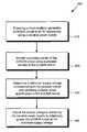
- FIG. 1is a conceptual block diagram showing a conventional local oscillator generator (LOGEN) circuit implementation in a transceiver.
- LOGENlocal oscillator generator
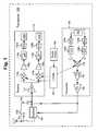
- FIG. 2is a conceptual block diagram of a transceiver including an adaptively powered LOGEN circuit, according to one embodiment of the present invention.
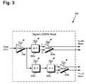
- FIG. 3illustrates a digital block of a LOGEN circuit receiving an adaptive supply voltage, according to one embodiment of the present invention.
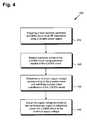
- FIG. 4is a flowchart presenting a method for adaptively powering a LOGEN circuit, according to one embodiment of the present invention.
- the present inventionis directed to an adaptively powered local oscillator generator (LOGEN) circuit and related method.
- LOGENlocal oscillator generator
- FIG. 1is a conceptual block diagram of transceiver 100 including conventional LOGEN circuit 150 powered by fixed supply voltage 106 .
- transceiver 100comprises antenna 102 , transceiver input/output routing switches 103 a and 103 b , duplexer 104 , transmit/receive (T/R) switch 105 , receiver 110 , and transmitter 130 .
- T/Rtransmit/receive
- LOGEN circuit 150 powered by fixed voltage supply 106is shared by receiver 110 and transmitter 130 , and is implemented to provide a drive signal to their respective mixer circuits.
- Receiver 110includes low noise amplifier (LNA) 112 , receiver mixers 114 a and 114 b working in conjunction with, respectively, in-phase (I) and quadrature-phase (Q) signals provided by LOGEN circuit 150 , and transimpedance amplifiers (TIAs) 116 a and 116 b . As also shown in FIG. 1 , receiver 110 further includes low-pass filters (LPFs) 118 a and 118 b , analog-to-digital converters (ADCs) 120 a and 120 b , and digital processors 122 a and 122 b , to perform back-end processing of the respective I and Q signal components.
- LPFslow-pass filters
- ADCsanalog-to-digital converters
- transmitter 130includes digital block 132 providing I and Q outputs to respective digital-to-analog converters (DACs) 134 a and 134 b .
- transmitter 130includes LPFs 136 a and 136 b , transmitter mixer 138 driven by LOGEN circuit 150 to combine and up-convert the I and Q signals to a transmit frequency, and power amplifier (PA) driver (pre-PA) 140 providing a preamplified transmit signal to PA 142 , which can be coupled to antenna 102 of transceiver 100 through duplexer 104 via transceiver input/output routing switch 103 a , or through T/R switch 105 via transceiver input/output routing switch 103 b , as also shown by FIG. 1 .
- PApower amplifier
- pre-PApreamplified transmit signal
- Drive strengthfor example rail-to-rail voltage swing, and low phase noise are important performance parameters for LOGEN circuit 150 .
- fixed supply voltage 106is set so as to satisfy specifications for those parameters even under the most unfavorable operating conditions.
- LOGEN circuit 150may be consistently powered to enable it to satisfy its phase noise and drive strength specifications for slow process corners at high temperature.
- LOGEN circuit 150comprising devices requiring a nominal 1.2V supply, may instead receive a constant supply of 1.26V, or higher, in order to assure adequate performance for slow process corners.
- the supply voltage actually required to satisfy the performance specifications for LOGEN circuit 150may vary considerably, depending upon whether fast, slow, or typical process corners are present, for example. Moreover, because neutral or favorable operating conditions, e.g., conditions corresponding to typical or fast process corners, respectively, may be at least as likely to prevail as the least favorable operating state, LOGEN circuit 150 is likely to be receiving a higher than needed supply voltage much of the time, resulting in unnecessary power consumption by transceiver 100 .
- any unnecessary power drainposes a substantial disadvantage.
- communications technologiescontinue to move in the direction of smaller device dimensions, higher device and system speeds, and smaller power supplies, as represented, for example, by the 40 nm technology node, the fundamental inefficiency represented by the conventional implementation shown in FIG. 1 becomes increasingly incongruous and undesirable.
- FIG. 2shows a conceptual block diagram of transceiver 200 including adaptively powered LOGEN circuit 250 , according to one embodiment of the present invention, capable of overcoming the disadvantages associated with the conventional implementation described above in relation to FIG. 1 .
- the innovative adaptively powered LOGEN of the present inventioncan be used in any RF component or device, including but not limited to a transceiver.
- the adaptively powered LOGEN of the present inventioncan be used in an RF receiver, an RF transmitter, or any other RF device, and not necessarily an RF transceiver.
- transceiver 200is used as specific example of any “RF device” in the present application.
- transceiver 200comprises antenna 202 , transceiver input/output routing switches 203 a and 203 b , duplexer 204 , T/R switch 205 , receiver 210 , and transmitter 230 .
- transceiver 200also comprises a variable power supply, shown in the embodiment of FIG. 2 as exemplary variable low-dropout regulator (LDO) 206 , LOGEN circuit 250 monitored by process monitor 260 , and LDO programming module 208 mediating communication between process monitor 260 and variable LDO 206 .
- LDOvariable low-dropout regulator
- process monitor 260is included as part of LOGEN circuit, while in others, process monitor 260 may be distinct from the circuitry comprised by LOGEN circuit 250 . In either set of embodiments, however, process monitor 260 and LOGEN circuit 250 are integrated on a common semiconductor die.
- process monitor 260is in communication with variable LDO 206 through LDO programming module 208 .
- LDO programming module 208shows variable LDO 206 and LDO programming module 208 , more generally those features correspond to any suitable combination of a variable power supply and a power supply programming module enabling communication between process monitor 260 and the variable power supply.
- FIG. 2depicts LDO programming module 208 as residing outside of variable LDO 206 , that embodiment is provided for conceptual clarity. In some embodiments, for example, LDO programming module 208 may be incorporated into variable LDO 206 .
- the particular embodiment shown in FIG. 2enables adaptive adjustment of the supply voltage provided to LOGEN circuit 250 according to actual LOGEN circuit performance data. That performance data may be supplied to variable LDO 206 by process monitor 260 through LDO programming module 208 , for example.
- Receiver 210 of transceiver 200includes LNA 212 , receiver mixers 214 a and 214 b working in conjunction with, respectively, I and Q signals provided by LOGEN circuit 250 , and TIAs 216 a and 216 b .
- Receiver 210is also shown to include LPFs 218 a and 218 b , ADCs 220 a and 220 b , and digital processors 222 a and 222 b , to perform back-end processing of the respective I and Q signal components.
- Transmitter 230 of transceiver 200includes digital block 232 providing I and Q outputs to respective DACs 234 a and 234 b .
- transmitter 230includes LPFs 236 a and 236 b , transmitter mixer 238 driven by LOGEN circuit 250 to combine and up-convert the I and Q signals to a transmit frequency, and pre-PA 240 providing a preamplified transmit signal to PA 242 , which can be coupled to antenna 202 of transceiver 200 through duplexer 204 via transceiver input/output routing switch 203 a , or through T/R switch 205 via transceiver input/output routing switch 203 b.
- Transceiver 200may be utilized in a cellular telephone or other mobile device communicating at radio frequency (RF), for example, such as in a frequency range from approximately 0.8 GHz to approximately 2.2 GHz, for example.
- RFradio frequency
- transceiver 200may be a multi-mode communication system, for example, capable of operating in one or more second-generation wireless telephone technology (2G) modes through use of routing switch 203 b and T/R switch 205 , and further configured to operate in one or more 3G modes through use of routing switch 203 a and duplexer 204 .
- 2Gsecond-generation wireless telephone technology
- LOGEN circuit 250is configured to be adaptively powered according to its actual supply voltage needs, as measured, for example, by its actual performance, rather than its worst case performance.
- the supply voltage actually required to satisfy the performance specifications for LOGEN circuit 250such as a phase noise or drive strength specification for LOGEN 250 , or some other performance constraint bearing on the operation of transceiver 200 , may vary considerably. That variance may depend, for example, upon whether fast, slow, or typical process corners characterize the actual performance of LOGEN circuit 250 during a particular time interval, and under actual performance conditions, such as temperature.
- the present approachenables dynamically adapting the supply voltage provided to LOGEN circuit according to its needs.
- the supply voltage provided to LOGEN circuit 250may be a minimum supply voltage for which a performance constraint of LOGEN circuit 250 , or transceiver 200 as a whole, is satisfied.
- process monitor 260may supply performance data regarding LOGEN circuit 250 corresponding to a process corner of LOGEN circuit 250 .
- variable LDO 206can adaptively adjust the supply voltage provided to LOGEN circuit 250 so as to provide, respectively a relatively high, moderate, or low supply voltage. Consequently, variable LDO may be dynamically responsive to the actual performance of LOGEN circuit 250 so as to provide a substantially minimum voltage necessary for LOGEN circuit 250 to satisfy its phase noise performance specification and to supply adequate drive strength.
- LOGEN circuit 250may receive an actual supply voltage ranging below 1.2V when fast process corners prevail, for example, rather receiving a fixed and constant supply of 1.2V, or higher, to assure adequate performance for slow process corners at all times, as in the conventional approach illustrated in FIG. 1 .
- LOGEN circuit 250may receive an actual supply voltage ranging above 1.2V to satisfy the circuit performance. This way, LOGEN circuit 250 can be designed using less power consumption for typical device corners. The overall power usage is much more efficient using this dynamic adjustment. In general, the power consumption rating is based on the power consumption in the typical device corners and typical temperatures.
- LOGEN circuit 250can enable significant and appropriately targeted reductions in the power consumed by LOGEN circuit 250 and receiver 200 as a whole.
- LOGEN circuit 250 , process monitor 260 , variable LDO 206 , and LDO programming module 208can be included with the constituents of receiver 210 , as well as digital block 232 , DACs 234 a and 234 b , LPFs 236 a and 236 b , transmitter mixer 238 , and pre-PA 240 of transmitter 230 on an integrated circuit (IC) fabricated on a single semiconductor die using a 40 nm process technology, for example.
- ICintegrated circuit
- FIG. 3shows a digital block of a LOGEN circuit configured to receive a variable supply voltage, according to one embodiment of the present invention.
- FIG. 4is a flowchart presenting a method for adaptively powering a LOGEN circuit, according to one embodiment of the present invention.
- FIG. 3shows digital LOGEN block 352 configured to receive an adaptive supply voltage, according to one embodiment of the present invention.
- digital LOGEN block 352is implemented as part of a LOGEN circuit, and is configured to receive an input signal from a voltage controlled oscillator (VCO) of the LOGEN circuit (VCO not shown in FIG. 3 ) and to provide output signals to high-band and low-band mixers of the LOGEN circuit (high-band and low-band mixers also not shown in FIG. 3 ). Thereafter, the suitably mixed high-band and low-band outputs signals of the LOGEN circuit may be provided as drive signals to a receiver or transmitter mixer.
- VCOvoltage controlled oscillator
- digital LOGEN block 352may correspond to digital circuitry within LOGEN circuit 250 , in FIG. 2 , which as described in conjunction with that previous figure is monitored by process monitor 260 . Consequently, the actual performance of digital LOGEN block 352 , in FIG. 3 , is also undergoing monitoring by a process monitor, such as process monitor 260 , in FIG. 2 .
- digital LOGEN block 352comprises input buffer 354 for receiving the input signal from the LOGEN circuit VCO, and both high-band and low-band signal generation paths coupled to the output of buffer 354 .
- a high-band signal generation pathmay include divide-by-two block 356 a and high-band buffer 358 a for buffering the I and Q outputs of divide-by-two block 356 a prior to outputting buffered I and Q signals to the high-band mixer of the LOGEN circuit.
- a low-band signal generation pathmay comprise sequential divide-by-two blocks 356 b and 356 c , and low-band buffer 358 b for buffering the I and Q outputs of divide-by-two block 356 c prior to outputting buffered I and Q signals to the low-band mixer of the LOGEN circuit, as represented in FIG. 3 .
- each of input buffer 354 , divide-by-two blocks 356 a , 356 b , and 356 c , and buffers 358 a and 358 bis configured to receive a variable supply V DD .
- Input buffer 354divide-by-two blocks 356 a , 356 b , and 356 c , and buffers 358 a and 358 b may be implemented as digital circuitry, as represented by their inclusion in digital LOGEN block 352 . Because the performance of digital circuit components is known to respond in a particularly predictable manner to variations in supply voltage, the adaptive power approach disclosed by embodiments of the present invention may prove to be especially advantageous when applied to digital circuitry, such as digital LOGEN block 352 .
- FIG. 4presents flowchart 400 describing one embodiment of a method for adaptively powering a LOGEN circuit.
- Certain details and featureshave been left out of flowchart 400 that are apparent to a person of ordinary skill in the art.
- a stepmay comprise one or more substeps or may involve specialized equipment or materials, as known in the art.
- steps 410 through 440 indicated in flowchart 400are sufficient to describe one embodiment of the present invention, other embodiments of the invention may utilize steps different from those shown in flowchart 400 , or may comprise more, or fewer, steps.
- Step 410 of flowchart 400comprises powering a LOGEN circuit of an RF transceiver using a variable power supply.
- step 410may be seen to correspond to powering LOGEN circuit 250 of transceiver 200 using variable LDO 206 .
- transceiver 200 including adaptively powered LOGEN circuit 250can be implemented in, for example, a wireless communications device, a cellular telephone, a Bluetooth enabled device, a computer, a satellite set-top box, an RF transceiver, a personal digital assistant (PDA), or in any other kind of system, device, component or module utilized as a transceiver in modern electronics applications.
- PDApersonal digital assistant
- step 410may correspond to providing LOGEN 250 with a default high supply voltage corresponding to performance under worst case operating conditions for example.
- step 410 of flowchart 400characterizes the present method as providing adaptive power to a LOGEN circuit, such as LOGEN circuit 250 , in FIG. 2 , more generally, the method described by flowchart 400 can be applied so as to adaptively power a variety of circuits. More specifically, and as described above, circuits comprising digital components are know to respond in a particularly predictable manner to variations in supply voltage, rendering the adaptive powering approach of the present method especially advantageous when applied to digital circuitry, which may comprise digital circuitry other than circuitry comprised by a LOGEN circuit.
- step 420 of flowchart 400comprises monitoring a process corner of the LOGEN circuit.
- step 420can be performed by process monitor 260 for LOGEN circuit 250 .
- process monitor 260may comprise a ring oscillator, fabricated as part of LOGEN circuit 250 , and implemented so as to sense whether a low, typical, or fast process corner corresponds to the actual performance profile of LOGEN circuit 250 at a particular point in time.
- step 430 of flowchart 400comprises determining a minimum supply voltage corresponding to the process corner identified through monitoring in step 420 , and satisfying a phase noise specification of LOGEN circuit 250 .
- Step 430may be performed by LDO programming module 208 , for example, which may be configured to determine a minimum supply voltage based on data supplied by process monitor 260 . More generally, LDO programming module 208 may be configured to determine a minimum supply voltage for LOGEN circuit 250 sufficient to satisfy any of a variety of performance constraints on LOGEN circuit 250 , or on transceiver 200 .
- step 440comprises adjusting the supply voltage provided by the variable power supply to adaptively power LOGEN circuit 250 at a minimum supply voltage.
- step 440may be performed by variable LDO 206 in response to a communication received from process monitor 260 through LDO programming module 208 .
- LDO programming module 208may write a code setting the output voltage of variable LDO 206 to a control registry of variable LDO 206 .
- Changes or updates to that code LDO programming module 208can result in adjustment of the supply voltage output by variable LDO 206 , thereby causing variable LDO 206 to adaptively adjust the supply voltage provided to LOGEN circuit 250 according to the actual performance of LOGEN circuit 250 , as measured by performance data supplied by process monitor 260 .
- embodiments of the present inventionenable an accurate assessment of the power needs of the digital circuit.
- embodiments of the present inventionenable an approach to dynamic power management capable of optimizing the power consumed by the digital circuit while satisfying its performance constraints.
- embodiments of the present inventionwhen implemented to adaptively power a LOGEN circuit comprised by an RF transceiver, enable adaptive adjustment of the supply voltage provided to the LOGEN circuit so as to substantially minimize the supply voltage while concurrently satisfying phase noise and drive strength requirements, thereby reducing power consumption by the LOGEN circuit and the RF transceiver as a whole, without compromising performance.
Landscapes
- Transceivers (AREA)
Abstract
Description
Claims (20)
Priority Applications (1)
| Application Number | Priority Date | Filing Date | Title |
|---|---|---|---|
| US12/802,604US9112508B2 (en) | 2010-06-09 | 2010-06-09 | Adaptive powered local oscillator generator circuit and related method |
Applications Claiming Priority (1)
| Application Number | Priority Date | Filing Date | Title |
|---|---|---|---|
| US12/802,604US9112508B2 (en) | 2010-06-09 | 2010-06-09 | Adaptive powered local oscillator generator circuit and related method |
Publications (2)
| Publication Number | Publication Date |
|---|---|
| US20110306311A1 US20110306311A1 (en) | 2011-12-15 |
| US9112508B2true US9112508B2 (en) | 2015-08-18 |
Family
ID=45096613
Family Applications (1)
| Application Number | Title | Priority Date | Filing Date |
|---|---|---|---|
| US12/802,604Expired - Fee RelatedUS9112508B2 (en) | 2010-06-09 | 2010-06-09 | Adaptive powered local oscillator generator circuit and related method |
Country Status (1)
| Country | Link |
|---|---|
| US (1) | US9112508B2 (en) |
Cited By (1)
| Publication number | Priority date | Publication date | Assignee | Title |
|---|---|---|---|---|
| US10887845B2 (en) | 2018-07-16 | 2021-01-05 | Samsung Electronics Co., Ltd. | Radio frequency integrated circuit including a local oscillator and operating method thereof |
Families Citing this family (4)
| Publication number | Priority date | Publication date | Assignee | Title |
|---|---|---|---|---|
| US8244198B1 (en)* | 2011-03-08 | 2012-08-14 | Texas Instruments Incorporated | Wireless device local oscillator generation apparatus and methods |
| US9480017B2 (en)* | 2013-02-11 | 2016-10-25 | Qualcomm Incorporated | Dynamic power management control |
| EP3226624A1 (en)* | 2016-03-31 | 2017-10-04 | Intel IP Corporation | Transceiver, transmitter, receiver and method for determining a minimum supply voltage for receivers and transmitters |
| US11349455B2 (en) | 2019-12-27 | 2022-05-31 | Industrial Technology Research Institute | Power divider, radio frequency transceiver and multi-stage power divider |
Citations (55)
| Publication number | Priority date | Publication date | Assignee | Title |
|---|---|---|---|---|
| US3652948A (en) | 1970-02-24 | 1972-03-28 | Motorola Inc | Power amplifier including plurality of push-pull amplifier sections coupled by ferrite matching transformers |
| JPS60145722A (en) | 1984-01-09 | 1985-08-01 | Hitachi Cable Ltd | Peak detection circuit |
| US4591795A (en) | 1984-10-01 | 1986-05-27 | United Technologies Corporation | Signal conditioning circuit for L/R VDT sensors |
| US4701722A (en) | 1985-06-17 | 1987-10-20 | Dolby Ray Milton | Circuit arrangements for modifying dynamic range using series and parallel circuit techniques |
| US4706262A (en) | 1984-03-30 | 1987-11-10 | Nec Corporation | FSK or FM burst signal generating apparatus |
| US4904921A (en) | 1987-11-13 | 1990-02-27 | Analog Devices, Inc. | Monolithic interface circuit for linear variable differential transformers |
| US5089716A (en) | 1989-04-06 | 1992-02-18 | Electromagnetic Sciences, Inc. | Simplified driver for controlled flux ferrite phase shifter |
| US5185581A (en) | 1992-03-26 | 1993-02-09 | Northern Telecom Limited | Differential amplifier and high frequency resonant circuits constructed therefrom |
| US5241694A (en) | 1989-05-12 | 1993-08-31 | Nokia Mobile Phones Ltd. | Circuit for forming low power levels in a transmitter of a radio telephone |
| US5432473A (en) | 1993-07-14 | 1995-07-11 | Nokia Mobile Phones, Limited | Dual mode amplifier with bias control |
| US5530923A (en) | 1994-03-30 | 1996-06-25 | Nokia Mobile Phones Ltd. | Dual mode transmission system with switched linear amplifier |
| US5606285A (en) | 1994-07-29 | 1997-02-25 | Oki Electric Industry Co., Ltd. | Power control circuit for use with transmitter |
| US5697074A (en) | 1995-03-30 | 1997-12-09 | Nokia Mobile Phones Limited | Dual rate power control loop for a transmitter |
| US5705957A (en)* | 1995-04-27 | 1998-01-06 | Seiko Epson Corporation | Temperature-compensated piezoelectric oscillator |
| US5777468A (en) | 1996-12-19 | 1998-07-07 | Texas Instruments Incorporated | Variable differential transformer system and method providing improved temperature stability and sensor fault detection apparatus |
| US6046641A (en) | 1998-07-22 | 2000-04-04 | Eni Technologies, Inc. | Parallel HV MOSFET high power stable amplifier |
| US6064262A (en) | 1998-09-25 | 2000-05-16 | Lucent Technologies Inc. | CMOS differential amplifier having offset voltage cancellation and common-mode voltage control |
| US6232842B1 (en) | 1998-03-13 | 2001-05-15 | Matsushita Electric Industrial Co., Ltd. | Amplifying circuit and optical receiver comprising the same |
| US6606359B1 (en) | 2000-07-26 | 2003-08-12 | Motorola, Inc | Area-optimum rapid acquisition cellular multi-protocol digital DC offset correction scheme |
| US20040087293A1 (en)* | 2002-11-04 | 2004-05-06 | Rolf Jaehne | Automatic center frequency tuning of a voltage controlled oscillator |
| US6864808B2 (en) | 2002-01-29 | 2005-03-08 | Goodrich Pump & Engine Control Systems, Inc. | System and method for processing a signal |
| US6900693B2 (en) | 2002-05-20 | 2005-05-31 | Sony Corporation | Power amplifying apparatus and radio communications apparatus using same |
| US20050118966A1 (en) | 2003-12-01 | 2005-06-02 | Kiomars Anvari | Simple Crest Factor reduction technique for multi-carrier signals |
| US20050218871A1 (en)* | 2003-04-11 | 2005-10-06 | Inyup Kang | Dynamic voltage scaling for portable devices |
| US20060009174A1 (en) | 2004-07-09 | 2006-01-12 | Doug Dunn | Variable-loss transmitter and method of operation |
| US20060105723A1 (en) | 2004-11-17 | 2006-05-18 | Kiomars Anvari | Simple crest factor reduction technique for non-constant envelope signals |
| US7076215B1 (en)* | 1999-03-12 | 2006-07-11 | Siemens Aktiengesellschaft | Transmitter-receiver |
| US20070070534A1 (en) | 2005-09-23 | 2007-03-29 | Aemireddy Arvind R | Variable threshold bipolar signal peak detector |
| US20070222525A1 (en)* | 2006-03-13 | 2007-09-27 | Kabushiki Kaisha Toshiba | Voltage controlled oscillator, operation current adjusting device, and operation current adjusting method of voltage controlled oscillator |
| US7305041B2 (en) | 2004-02-20 | 2007-12-04 | Kiomars Anvari | Peak suppression of multi-carrier signal with different modulation |
| US20080003960A1 (en) | 2006-06-29 | 2008-01-03 | Alireza Zolfaghari | Polar transmitter amplifier with variable output power |
| US20080076363A1 (en) | 2006-09-27 | 2008-03-27 | Rafi Aslamali A | Integrating an FM transmitter into a cellular telephone |
| US20080076372A1 (en)* | 2006-09-26 | 2008-03-27 | Timothy Nutt | Reducing power dissipation using process corner information |
| US7382166B1 (en) | 2006-05-16 | 2008-06-03 | Fujitsu Limited | Signal amplification device |
| US20080155282A1 (en)* | 2006-12-21 | 2008-06-26 | Texas Instruments, Inc. | Adaptive voltage scaling with age compensation |
| US7471935B2 (en) | 2000-10-23 | 2008-12-30 | Intel Corporation | Automatic level control |
| US7477187B2 (en) | 2007-03-29 | 2009-01-13 | Broadcom Corporation | Wireless communication device having GPS receiver and an on-chip gyrator |
| US20090073070A1 (en) | 2007-03-30 | 2009-03-19 | Broadcom Corporation | Dual band antenna and methods for use therewith |
| US7525347B1 (en) | 2006-10-20 | 2009-04-28 | Marvell International Ltd. | Differential peak detector |
| US20090130994A1 (en)* | 2007-11-20 | 2009-05-21 | Qualcomm Incorporated | Adjustable local oscillator path in a communication device with a transmitter |
| US7539466B2 (en) | 2004-12-14 | 2009-05-26 | Motorola, Inc. | Amplifier with varying supply voltage and input attenuation based upon supply voltage |
| US7581120B1 (en)* | 2005-05-23 | 2009-08-25 | National Semiconductor Corporation | System and method for providing multi-point calibration of an adaptive voltage scaling system |
| US20090298415A1 (en)* | 2008-06-02 | 2009-12-03 | Qualcomm Incorporated | Methods and apparatus for power reduction in a transceiver |
| US20100090760A1 (en) | 2008-10-14 | 2010-04-15 | Paratek Microwave, Inc. | Low-distortion voltage variable capacitor assemblies |
| US20100099369A1 (en) | 2008-10-16 | 2010-04-22 | Texas Instruments Incorporated | Automatic frequency tuning system and method for an fm-band transmit power amplifier |
| US20100159856A1 (en) | 2008-12-22 | 2010-06-24 | Kabushiki Kaisha Toshiba | Distortion compensator, distortion compensation method, and transmitter |
| US20100266066A1 (en) | 2007-11-05 | 2010-10-21 | Nec Corporation | Power amplifier and radio wave transmitter having the same |
| US20100321124A1 (en)* | 2009-06-17 | 2010-12-23 | Qualcomm Incorporated | Configurable wide tuning range oscillator core |
| US20110057732A1 (en)* | 2009-09-10 | 2011-03-10 | Taylor Stewart S | Low phase noise voltage controlled oscillator |
| US20110076972A1 (en)* | 2009-09-29 | 2011-03-31 | Daniel Cooley | Systems and methods for tuning a broadcast radio receiver with digital display |
| US8026743B2 (en) | 2008-08-15 | 2011-09-27 | Taiwan Semiconductor Manufacturing Company, Ltd. | Envelope detector for high speed applications |
| US20120046004A1 (en) | 2010-08-19 | 2012-02-23 | Broadcom Corporation | High performance transmitter preamplification chain with calibration feedback |
| US20120052824A1 (en) | 2010-08-30 | 2012-03-01 | Broadcom Corporation | Variable gain control transformer and RF transmitter utilizing same |
| US8260227B2 (en) | 2008-06-10 | 2012-09-04 | Mediatek Inc. | Direct conversion receiver and DC offset concellation method |
| US8311155B2 (en) | 2007-12-26 | 2012-11-13 | Panasonic Corporation | Electronic tuner and high frequency receiving device using the same |
- 2010
- 2010-06-09USUS12/802,604patent/US9112508B2/ennot_activeExpired - Fee Related
Patent Citations (56)
| Publication number | Priority date | Publication date | Assignee | Title |
|---|---|---|---|---|
| US3652948A (en) | 1970-02-24 | 1972-03-28 | Motorola Inc | Power amplifier including plurality of push-pull amplifier sections coupled by ferrite matching transformers |
| JPS60145722A (en) | 1984-01-09 | 1985-08-01 | Hitachi Cable Ltd | Peak detection circuit |
| US4706262A (en) | 1984-03-30 | 1987-11-10 | Nec Corporation | FSK or FM burst signal generating apparatus |
| US4591795A (en) | 1984-10-01 | 1986-05-27 | United Technologies Corporation | Signal conditioning circuit for L/R VDT sensors |
| US4701722A (en) | 1985-06-17 | 1987-10-20 | Dolby Ray Milton | Circuit arrangements for modifying dynamic range using series and parallel circuit techniques |
| US4904921A (en) | 1987-11-13 | 1990-02-27 | Analog Devices, Inc. | Monolithic interface circuit for linear variable differential transformers |
| US5089716A (en) | 1989-04-06 | 1992-02-18 | Electromagnetic Sciences, Inc. | Simplified driver for controlled flux ferrite phase shifter |
| US5241694A (en) | 1989-05-12 | 1993-08-31 | Nokia Mobile Phones Ltd. | Circuit for forming low power levels in a transmitter of a radio telephone |
| US5185581A (en) | 1992-03-26 | 1993-02-09 | Northern Telecom Limited | Differential amplifier and high frequency resonant circuits constructed therefrom |
| US5432473A (en) | 1993-07-14 | 1995-07-11 | Nokia Mobile Phones, Limited | Dual mode amplifier with bias control |
| US5530923A (en) | 1994-03-30 | 1996-06-25 | Nokia Mobile Phones Ltd. | Dual mode transmission system with switched linear amplifier |
| US5606285A (en) | 1994-07-29 | 1997-02-25 | Oki Electric Industry Co., Ltd. | Power control circuit for use with transmitter |
| US5697074A (en) | 1995-03-30 | 1997-12-09 | Nokia Mobile Phones Limited | Dual rate power control loop for a transmitter |
| US5705957A (en)* | 1995-04-27 | 1998-01-06 | Seiko Epson Corporation | Temperature-compensated piezoelectric oscillator |
| US5777468A (en) | 1996-12-19 | 1998-07-07 | Texas Instruments Incorporated | Variable differential transformer system and method providing improved temperature stability and sensor fault detection apparatus |
| US6232842B1 (en) | 1998-03-13 | 2001-05-15 | Matsushita Electric Industrial Co., Ltd. | Amplifying circuit and optical receiver comprising the same |
| US6046641A (en) | 1998-07-22 | 2000-04-04 | Eni Technologies, Inc. | Parallel HV MOSFET high power stable amplifier |
| US6064262A (en) | 1998-09-25 | 2000-05-16 | Lucent Technologies Inc. | CMOS differential amplifier having offset voltage cancellation and common-mode voltage control |
| US7076215B1 (en)* | 1999-03-12 | 2006-07-11 | Siemens Aktiengesellschaft | Transmitter-receiver |
| US6606359B1 (en) | 2000-07-26 | 2003-08-12 | Motorola, Inc | Area-optimum rapid acquisition cellular multi-protocol digital DC offset correction scheme |
| US7471935B2 (en) | 2000-10-23 | 2008-12-30 | Intel Corporation | Automatic level control |
| US6864808B2 (en) | 2002-01-29 | 2005-03-08 | Goodrich Pump & Engine Control Systems, Inc. | System and method for processing a signal |
| US6900693B2 (en) | 2002-05-20 | 2005-05-31 | Sony Corporation | Power amplifying apparatus and radio communications apparatus using same |
| US20040087293A1 (en)* | 2002-11-04 | 2004-05-06 | Rolf Jaehne | Automatic center frequency tuning of a voltage controlled oscillator |
| US20050218871A1 (en)* | 2003-04-11 | 2005-10-06 | Inyup Kang | Dynamic voltage scaling for portable devices |
| US20050118966A1 (en) | 2003-12-01 | 2005-06-02 | Kiomars Anvari | Simple Crest Factor reduction technique for multi-carrier signals |
| US7305041B2 (en) | 2004-02-20 | 2007-12-04 | Kiomars Anvari | Peak suppression of multi-carrier signal with different modulation |
| US20060009174A1 (en) | 2004-07-09 | 2006-01-12 | Doug Dunn | Variable-loss transmitter and method of operation |
| US20060105723A1 (en) | 2004-11-17 | 2006-05-18 | Kiomars Anvari | Simple crest factor reduction technique for non-constant envelope signals |
| US7539466B2 (en) | 2004-12-14 | 2009-05-26 | Motorola, Inc. | Amplifier with varying supply voltage and input attenuation based upon supply voltage |
| US7581120B1 (en)* | 2005-05-23 | 2009-08-25 | National Semiconductor Corporation | System and method for providing multi-point calibration of an adaptive voltage scaling system |
| US20070070534A1 (en) | 2005-09-23 | 2007-03-29 | Aemireddy Arvind R | Variable threshold bipolar signal peak detector |
| US7626777B2 (en) | 2005-09-23 | 2009-12-01 | Agere Systems Inc. | Variable threshold bipolar signal peak detector |
| US20070222525A1 (en)* | 2006-03-13 | 2007-09-27 | Kabushiki Kaisha Toshiba | Voltage controlled oscillator, operation current adjusting device, and operation current adjusting method of voltage controlled oscillator |
| US7382166B1 (en) | 2006-05-16 | 2008-06-03 | Fujitsu Limited | Signal amplification device |
| US20080003960A1 (en) | 2006-06-29 | 2008-01-03 | Alireza Zolfaghari | Polar transmitter amplifier with variable output power |
| US20080076372A1 (en)* | 2006-09-26 | 2008-03-27 | Timothy Nutt | Reducing power dissipation using process corner information |
| US20080076363A1 (en) | 2006-09-27 | 2008-03-27 | Rafi Aslamali A | Integrating an FM transmitter into a cellular telephone |
| US7525347B1 (en) | 2006-10-20 | 2009-04-28 | Marvell International Ltd. | Differential peak detector |
| US20080155282A1 (en)* | 2006-12-21 | 2008-06-26 | Texas Instruments, Inc. | Adaptive voltage scaling with age compensation |
| US7477187B2 (en) | 2007-03-29 | 2009-01-13 | Broadcom Corporation | Wireless communication device having GPS receiver and an on-chip gyrator |
| US20090073070A1 (en) | 2007-03-30 | 2009-03-19 | Broadcom Corporation | Dual band antenna and methods for use therewith |
| US20100266066A1 (en) | 2007-11-05 | 2010-10-21 | Nec Corporation | Power amplifier and radio wave transmitter having the same |
| US20090130994A1 (en)* | 2007-11-20 | 2009-05-21 | Qualcomm Incorporated | Adjustable local oscillator path in a communication device with a transmitter |
| US8311155B2 (en) | 2007-12-26 | 2012-11-13 | Panasonic Corporation | Electronic tuner and high frequency receiving device using the same |
| US20090298415A1 (en)* | 2008-06-02 | 2009-12-03 | Qualcomm Incorporated | Methods and apparatus for power reduction in a transceiver |
| US8260227B2 (en) | 2008-06-10 | 2012-09-04 | Mediatek Inc. | Direct conversion receiver and DC offset concellation method |
| US8026743B2 (en) | 2008-08-15 | 2011-09-27 | Taiwan Semiconductor Manufacturing Company, Ltd. | Envelope detector for high speed applications |
| US20100090760A1 (en) | 2008-10-14 | 2010-04-15 | Paratek Microwave, Inc. | Low-distortion voltage variable capacitor assemblies |
| US20100099369A1 (en) | 2008-10-16 | 2010-04-22 | Texas Instruments Incorporated | Automatic frequency tuning system and method for an fm-band transmit power amplifier |
| US20100159856A1 (en) | 2008-12-22 | 2010-06-24 | Kabushiki Kaisha Toshiba | Distortion compensator, distortion compensation method, and transmitter |
| US20100321124A1 (en)* | 2009-06-17 | 2010-12-23 | Qualcomm Incorporated | Configurable wide tuning range oscillator core |
| US20110057732A1 (en)* | 2009-09-10 | 2011-03-10 | Taylor Stewart S | Low phase noise voltage controlled oscillator |
| US20110076972A1 (en)* | 2009-09-29 | 2011-03-31 | Daniel Cooley | Systems and methods for tuning a broadcast radio receiver with digital display |
| US20120046004A1 (en) | 2010-08-19 | 2012-02-23 | Broadcom Corporation | High performance transmitter preamplification chain with calibration feedback |
| US20120052824A1 (en) | 2010-08-30 | 2012-03-01 | Broadcom Corporation | Variable gain control transformer and RF transmitter utilizing same |
Cited By (1)
| Publication number | Priority date | Publication date | Assignee | Title |
|---|---|---|---|---|
| US10887845B2 (en) | 2018-07-16 | 2021-01-05 | Samsung Electronics Co., Ltd. | Radio frequency integrated circuit including a local oscillator and operating method thereof |
Also Published As
| Publication number | Publication date |
|---|---|
| US20110306311A1 (en) | 2011-12-15 |
Similar Documents
| Publication | Publication Date | Title |
|---|---|---|
| US10187137B2 (en) | High power user equipment (HPUE) using coherently combined power amplifiers | |
| RU2433529C2 (en) | Variable linearity sps receiver | |
| US8862064B2 (en) | Self-testing transceiver architecture and related method | |
| US11044671B2 (en) | Communication system including a wake-up radio | |
| US9112508B2 (en) | Adaptive powered local oscillator generator circuit and related method | |
| JP4931936B2 (en) | Transmission device and communication device | |
| US20080157875A1 (en) | Method and System for Precise Current Matching in Deep Sub-Micron Technology | |
| EP2449675B1 (en) | Gain control linearity in an rf driver amplifier transmitter | |
| US9480017B2 (en) | Dynamic power management control | |
| EP3264706B1 (en) | Low drop out compensation technique for reduced dynamic errors in digital-to-time converters | |
| JP2006190021A (en) | Semiconductor integrated circuit device and radio communication system | |
| US10454665B2 (en) | Hybrid-controlled clock generation | |
| US9929737B2 (en) | Oscillator arrangement, method, computer program and communication device | |
| KR100950618B1 (en) | Efficient Radio Frequency Driver System with Linear Power with Power Level Control | |
| US9008600B2 (en) | Wireless communication receiver having one signal processing circuit whose operation mode is adjusted by monitoring signal level of specific signal of preceding signal processing circuit and related wireless communication method | |
| US20080136498A1 (en) | Method and System for Buffering A Clock Signal | |
| US20240427409A1 (en) | Electrical device with a deep sleep mode implemented with a level shifter | |
| US20160352370A1 (en) | Local oscillation signal level adjustment circuit, local oscillation signal level adjustment method, and wireless communication device | |
| KR100517633B1 (en) | Output power control circuit of power amplifier | |
| KR101072075B1 (en) | Radio frequency communication device and power cotrol method thereof | |
| JP2016225969A (en) | Local oscillation signal level adjustment circuit, local oscillation signal level adjustment method, and radio communication device | |
| HK1167942B (en) | Self-testing transceiver and self-testing method thereof |
Legal Events
| Date | Code | Title | Description |
|---|---|---|---|
| AS | Assignment | Owner name:BROADCOM CORPORATION, CALIFORNIA Free format text:ASSIGNMENT OF ASSIGNORS INTEREST;ASSIGNORS:CHANG, YUYU;YAZDI, AHMAD;DARABI, HOOMAN;REEL/FRAME:024628/0071 Effective date:20100602 | |
| STCF | Information on status: patent grant | Free format text:PATENTED CASE | |
| AS | Assignment | Owner name:BANK OF AMERICA, N.A., AS COLLATERAL AGENT, NORTH CAROLINA Free format text:PATENT SECURITY AGREEMENT;ASSIGNOR:BROADCOM CORPORATION;REEL/FRAME:037806/0001 Effective date:20160201 Owner name:BANK OF AMERICA, N.A., AS COLLATERAL AGENT, NORTH Free format text:PATENT SECURITY AGREEMENT;ASSIGNOR:BROADCOM CORPORATION;REEL/FRAME:037806/0001 Effective date:20160201 | |
| AS | Assignment | Owner name:AVAGO TECHNOLOGIES GENERAL IP (SINGAPORE) PTE. LTD., SINGAPORE Free format text:ASSIGNMENT OF ASSIGNORS INTEREST;ASSIGNOR:BROADCOM CORPORATION;REEL/FRAME:041706/0001 Effective date:20170120 Owner name:AVAGO TECHNOLOGIES GENERAL IP (SINGAPORE) PTE. LTD Free format text:ASSIGNMENT OF ASSIGNORS INTEREST;ASSIGNOR:BROADCOM CORPORATION;REEL/FRAME:041706/0001 Effective date:20170120 | |
| AS | Assignment | Owner name:BROADCOM CORPORATION, CALIFORNIA Free format text:TERMINATION AND RELEASE OF SECURITY INTEREST IN PATENTS;ASSIGNOR:BANK OF AMERICA, N.A., AS COLLATERAL AGENT;REEL/FRAME:041712/0001 Effective date:20170119 | |
| AS | Assignment | Owner name:AVAGO TECHNOLOGIES INTERNATIONAL SALES PTE. LIMITE Free format text:MERGER;ASSIGNOR:AVAGO TECHNOLOGIES GENERAL IP (SINGAPORE) PTE. LTD.;REEL/FRAME:047229/0408 Effective date:20180509 | |
| AS | Assignment | Owner name:AVAGO TECHNOLOGIES INTERNATIONAL SALES PTE. LIMITE Free format text:CORRECTIVE ASSIGNMENT TO CORRECT THE EFFECTIVE DATE PREVIOUSLY RECORDED ON REEL 047229 FRAME 0408. ASSIGNOR(S) HEREBY CONFIRMS THE THE EFFECTIVE DATE IS 09/05/2018;ASSIGNOR:AVAGO TECHNOLOGIES GENERAL IP (SINGAPORE) PTE. LTD.;REEL/FRAME:047349/0001 Effective date:20180905 | |
| AS | Assignment | Owner name:AVAGO TECHNOLOGIES INTERNATIONAL SALES PTE. LIMITE Free format text:CORRECTIVE ASSIGNMENT TO CORRECT THE PATENT NUMBER 9,385,856 TO 9,385,756 PREVIOUSLY RECORDED AT REEL: 47349 FRAME: 001. ASSIGNOR(S) HEREBY CONFIRMS THE MERGER;ASSIGNOR:AVAGO TECHNOLOGIES GENERAL IP (SINGAPORE) PTE. LTD.;REEL/FRAME:051144/0648 Effective date:20180905 | |
| FEPP | Fee payment procedure | Free format text:MAINTENANCE FEE REMINDER MAILED (ORIGINAL EVENT CODE: REM.); ENTITY STATUS OF PATENT OWNER: LARGE ENTITY | |
| LAPS | Lapse for failure to pay maintenance fees | Free format text:PATENT EXPIRED FOR FAILURE TO PAY MAINTENANCE FEES (ORIGINAL EVENT CODE: EXP.); ENTITY STATUS OF PATENT OWNER: LARGE ENTITY | |
| STCH | Information on status: patent discontinuation | Free format text:PATENT EXPIRED DUE TO NONPAYMENT OF MAINTENANCE FEES UNDER 37 CFR 1.362 | |
| FP | Expired due to failure to pay maintenance fee | Effective date:20190818 |