US9112484B1 - Integrated circuit process and bias monitors and related methods - Google Patents
Integrated circuit process and bias monitors and related methodsDownload PDFInfo
- Publication number
- US9112484B1 US9112484B1US14/136,258US201314136258AUS9112484B1US 9112484 B1US9112484 B1US 9112484B1US 201314136258 AUS201314136258 AUS 201314136258AUS 9112484 B1US9112484 B1US 9112484B1
- Authority
- US
- United States
- Prior art keywords
- transistor
- circuit
- mirror
- coupled
- stage
- Prior art date
- Legal status (The legal status is an assumption and is not a legal conclusion. Google has not performed a legal analysis and makes no representation as to the accuracy of the status listed.)
- Active
Links
Images


Classifications
- H—ELECTRICITY
- H03—ELECTRONIC CIRCUITRY
- H03K—PULSE TECHNIQUE
- H03K3/00—Circuits for generating electric pulses; Monostable, bistable or multistable circuits
- H03K3/01—Details
- H03K3/011—Modifications of generator to compensate for variations in physical values, e.g. voltage, temperature
- G—PHYSICS
- G01—MEASURING; TESTING
- G01R—MEASURING ELECTRIC VARIABLES; MEASURING MAGNETIC VARIABLES
- G01R31/00—Arrangements for testing electric properties; Arrangements for locating electric faults; Arrangements for electrical testing characterised by what is being tested not provided for elsewhere
- G01R31/28—Testing of electronic circuits, e.g. by signal tracer
- G01R31/2851—Testing of integrated circuits [IC]
- G01R31/2884—Testing of integrated circuits [IC] using dedicated test connectors, test elements or test circuits on the IC under test
- G—PHYSICS
- G05—CONTROLLING; REGULATING
- G05F—SYSTEMS FOR REGULATING ELECTRIC OR MAGNETIC VARIABLES
- G05F3/00—Non-retroactive systems for regulating electric variables by using an uncontrolled element, or an uncontrolled combination of elements, such element or such combination having self-regulating properties
- G05F3/02—Regulating voltage or current
- G05F3/08—Regulating voltage or current wherein the variable is DC
- G05F3/10—Regulating voltage or current wherein the variable is DC using uncontrolled devices with non-linear characteristics
- G05F3/16—Regulating voltage or current wherein the variable is DC using uncontrolled devices with non-linear characteristics being semiconductor devices
- G05F3/20—Regulating voltage or current wherein the variable is DC using uncontrolled devices with non-linear characteristics being semiconductor devices using diode- transistor combinations
- G05F3/205—Substrate bias-voltage generators
- G—PHYSICS
- G05—CONTROLLING; REGULATING
- G05F—SYSTEMS FOR REGULATING ELECTRIC OR MAGNETIC VARIABLES
- G05F3/00—Non-retroactive systems for regulating electric variables by using an uncontrolled element, or an uncontrolled combination of elements, such element or such combination having self-regulating properties
- G05F3/02—Regulating voltage or current
- G05F3/08—Regulating voltage or current wherein the variable is DC
- G05F3/10—Regulating voltage or current wherein the variable is DC using uncontrolled devices with non-linear characteristics
- G05F3/16—Regulating voltage or current wherein the variable is DC using uncontrolled devices with non-linear characteristics being semiconductor devices
- G05F3/20—Regulating voltage or current wherein the variable is DC using uncontrolled devices with non-linear characteristics being semiconductor devices using diode- transistor combinations
- G05F3/26—Current mirrors
- G05F3/262—Current mirrors using field-effect transistors only
- H—ELECTRICITY
- H03—ELECTRONIC CIRCUITRY
- H03K—PULSE TECHNIQUE
- H03K3/00—Circuits for generating electric pulses; Monostable, bistable or multistable circuits
- H03K3/02—Generators characterised by the type of circuit or by the means used for producing pulses
- H03K3/027—Generators characterised by the type of circuit or by the means used for producing pulses by the use of logic circuits, with internal or external positive feedback
- H03K3/03—Astable circuits
- H03K3/0315—Ring oscillators
- H—ELECTRICITY
- H01—ELECTRIC ELEMENTS
- H01L—SEMICONDUCTOR DEVICES NOT COVERED BY CLASS H10
- H01L22/00—Testing or measuring during manufacture or treatment; Reliability measurements, i.e. testing of parts without further processing to modify the parts as such; Structural arrangements therefor
- H01L22/30—Structural arrangements specially adapted for testing or measuring during manufacture or treatment, or specially adapted for reliability measurements
- H01L22/34—Circuits for electrically characterising or monitoring manufacturing processes, e. g. whole test die, wafers filled with test structures, on-board-devices incorporated on each die, process control monitors or pad structures thereof, devices in scribe line
- H—ELECTRICITY
- H10—SEMICONDUCTOR DEVICES; ELECTRIC SOLID-STATE DEVICES NOT OTHERWISE PROVIDED FOR
- H10D—INORGANIC ELECTRIC SEMICONDUCTOR DEVICES
- H10D30/00—Field-effect transistors [FET]
- H10D30/60—Insulated-gate field-effect transistors [IGFET]
- H10D30/62—Fin field-effect transistors [FinFET]
- H10D30/6211—Fin field-effect transistors [FinFET] having fin-shaped semiconductor bodies integral with the bulk semiconductor substrates
Definitions
- the present inventionrelates generally to circuits to monitor integrated circuit performance, and more particularly to ring oscillator stages designed to reflect the performance of certain transistors types.
- RDFRandom Dopant Fluctuation
- Other reasons for this variationinclude dopant scattering effect, such as the well proximity effect, that makes the placement of dopants in MOSFET transistors increasingly difficult as transistor size is reduced.
- Misplaced dopantscan reduce transistor performance, increase transistor variability, including variability of channel transconductance, capacitance effects, threshold voltage, and leakage. Such variability increases as transistors are reduced in size, with each misplaced dopant atom having a greater relative effect on transistor properties, as a result of the overall reduction in the number of dopant atoms.
- IC devicesuse a variety of cells that perform specific functions.
- IC devicescan include logic, memory, controller and other functional blocks.
- Semiconductor IC devicesare fabricated in a semiconductor process, often using a complementary metal-oxide-semiconductor (CMOS) process.
- CMOScomplementary metal-oxide-semiconductor
- Transistorsare formed in a semiconductor substrate, and usually involve a sequence of fabrication steps that result in a gate with adjacent source and drain, the source and drain being formed in a channel.
- an IC devicecan include different transistor device types including p-channel MOS (PMOS) transistors, n-channel MOS (NMOS) transistors, MOS field effect transistors (MOSFETs) tailored for digital or analog applications, high-voltage MOSFETs, high/normal/low frequency MOSFETs, MOSFETs optimized to work at distinct voltages or voltage ranges, low/high power MOSFETs, and low, regular, or high threshold voltage (Vt) transistors (i.e., low Vt (LVT), standard Vt (SVT), or high Vt (HVT)), etc.
- PMOSp-channel MOS
- NMOSn-channel MOS
- MOSFETsMOS field effect transistors
- Vtthreshold voltage
- Transistor device typesare usually distinguished by electrical performance characteristics (e.g., threshold voltage, speed, mobility, transconductance, linearity, noise, power), which can in turn lend themselves to be suitable for a particular application (e.g., signal processing, or data storage). Therefore, a complex IC device such as, for instance, a system on a chip (SoC), can use different transistor types (or a combination of one or more different transistor types) to achieve the target performance for different circuit blocks in the IC device.
- SoCsystem on a chip
- the electrical performance characteristics of the different transistor device types in a SoCcan be subject to variation due to manufacturing process variations, also referred to as the “manufacturing corner” of a particular transistor device.
- the electrical performance variation of the different transistor device types of the SoCcan be different because the performance of each transistor device type is impacted differently by the manufacturing process variations.
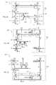
- FIG. 1Ais a block schematic view of a monitor circuit according to an embodiment.
- FIG. 1Bis a block schematic diagram of a ring oscillator monitor circuit according to an embodiment.
- FIG. 1Cis schematic diagram of a monitor circuit according to another embodiment.
- FIGS. 2A to 2Dare schematic diagrams of monitor circuits according to various other embodiments.
- FIGS. 3A and 3Bare graphs showing how delays produced by monitor circuits, according to embodiments, vary according to transistor variation.
- FIG. 4is a graph showing the delay introduced by a ring oscillator circuit, having an n-channel reference transistor according to an embodiment, in response to process variation
- FIG. 5Ais a graph showing the delay introduced by a ring oscillator circuit, having an n-channel reference transistor, for body bias variations in both n-channel and p-channel transistors, according to embodiments.
- FIG. 5Bis a graph showing the delay introduced by a ring oscillator circuit, having an n-channel reference transistor, for n-channel body bias variations and process variation corners, according to embodiments.
- FIG. 5Cis a graph showing the delay introduced by a ring oscillator circuit, having an n-channel reference transistor, for p-channel body bias variations and process variation corners, according to embodiments.
- FIG. 5Dis a graph showing the delay introduced by a ring oscillator circuit, having a p-channel reference transistor, for p-channel body bias variations and process variation corners, according to embodiments.
- FIG. 5Eis a graph showing the delay introduced by a ring oscillator circuit, having a p-channel reference transistor, for n-channel body bias variations and process variation corners, according to embodiments.
- FIGS. 6A to 6Care schematic diagrams of monitor circuits that can be disabled according to various other embodiments.
- FIGS. 7A to 7Care side cross sectional representations of transistors that can be included in embodiments.
- FIG. 8is a block schematic diagram of an integrated circuit device according to an embodiment.
- process monitor circuitscan be used to determine the electrical performance variation of the different transistor types as a result of variations, including but not limited to: manufacturing process variations, body bias conditions, and/or operating conditions (e.g., temperature, supply voltage).
- manufacturing process variationse.g., temperature, supply voltage
- operating conditionse.g., temperature, supply voltage
- FIG. 1Ais a block schematic diagram of a monitor circuit 100 according to one embodiment.
- Monitor circuit 100can vary a speed at which one or more output signals (OUT(s)) are generated from one or more input signals (IN(s)), based on the performance of one or more reference transistors 122 .
- the performance of the monitor circuit 100can vary in response to variation in the reference transistor(s) 122 .
- variations in a reference transistorcan arise from process variations, bias conditions, other operating conditions, or combinations thereof.
- a monitor circuit 100can include a current mirror section 105 and switching section 124 disposed between a first power supply node V 1 and a second power supply node V 2 .
- a current mirror section 105can include a current mirror circuit 120 and reference transistor(s) 122 .
- a current mirror circuit 120can include any suitable current mirror circuit that can mirror a current generated with reference transistor(s) 122 (i N ) to generate a mirrored current (i M ) for use by switching circuit 124 .
- a direction of currents i N and i Mcan vary according to the current mirror configuration (e.g., transistor conductivity type).
- a current mirror circuit 120can be formed with transistors that are larger than reference transistor(s) 122 , so that a current i N can vary predominantly according to reference transistor(s) 122 , and substantially not in response to transistors of the current mirror circuit 120 . More particularly, transistors of current mirror circuit 120 can have longer channels than those of reference transistor(s) 122 . In some embodiments, transistors of current mirror circuit 120 can have channels that are both longer and wider than those of reference transistor(s) 122 . Moreover, the reference transistor(s) 122 may be configured to match the performance of one or more of the switching circuit 124 transistors.
- i NK*i M , where K is greater than, or less than one.
- Reference transistor(s) 122can be of an opposite conductivity type to transistors of current mirror circuit 120 .
- a reference transistor 122can be arranged so that the reference current i N flows through its source-drain path.
- a reference transistor 122can be an insulated gate field effect transistor, referred to herein as a metal-oxide-semiconductor (MOS) transistor, but implying no particular type of gate insulator.
- MOSmetal-oxide-semiconductor
- reference transistor(s) 122can include an n-channel (NMOS) transistor MN (in which case current mirror circuit 120 can be formed with p-channel MOS (PMOS) transistors) or a PMOS transistor MP (in which case current mirror circuit 120 can be formed with NMOS transistors).
- Switching section 124can receive one or more input signals (IN(s)), and generate therefrom one or more output signals (OUT(s)). A speed at which a corresponding output signal can be generated can vary according to the mirrored current i M . In some embodiments, switching circuit 124 can logically invert input signal(s) IN(s) to generate output signals OUT(s).
- monitor circuit 100can be one stage of a ring oscillator circuit composed of many such stages.
- Input signal(s) IN(s)can be output signals received from another stage of the ring oscillator circuit.
- output signal(s) OUT(s)can be provided as input signals for another stage of the ring oscillator circuit.
- FIG. 1Bis a block schematic diagram of a ring oscillator monitor circuit 150 according to an embodiment.
- a circuit 150can include a ring oscillator circuit 152 and a delay monitor circuit 154 .
- a ring oscillator circuit 152can include a number of stages 100 - 0 to 100 - n arranged in a ring to generate an oscillating signal OSC having a frequency that varies according to the delay of each stage ( 100 - 0 to -n).
- Stages ( 100 - 0 to -n)can take the form of any of the monitor circuits shown herein, or equivalents.
- a delay introduced by one or all stagescan vary according to the reference transistors included within such stages, or in an embodiment where the reference and switching circuits are meant to have the same performance, to both the switching and reference devices of the reference type. Accordingly, an oscillating signal (OSC) speed/period will also vary according to the reference transistor(s).
- OSCoscillating signal
- a delay monitor circuit 154can determine the speed of oscillating signal (OSC) according to any suitable technique (for instance, by measuring the period of oscillation). From such a value, the performance of reference transistors can be determined.
- OSCspeed of oscillating signal
- ring oscillator monitor circuit 150can be formed in an integrated circuit (IC) device having other sections formed with transistors that match the reference transistors (i.e., are created with same fabrication process steps, but are not necessarily the same size).
- the performance of the reference transistorscan thus reflect the performance of the transistors in such other sections.
- the operation conditions of the other transistors in the other sectionscan be adjusted.
- Such adjustmentscan take any suitable form, including changing a body biasing, a power supply level, or configuring field programmable circuits to vary signals paths, as but a few examples.
- FIG. 1Cshows a monitor circuit 100 ′ according to another embodiment.
- a monitor circuit 100 ′can be one stage of a ring oscillator circuit that can be used to measure the variation of NMOS transistors with substantially no contribution from the variation of PMOS transistors.
- a monitor circuit 100 ′can be one very particular implementation of that shown in FIG. 1A .
- a monitor circuit 100 ′can include a current mirror section 105 ′ and switching section 124 ′.
- Current mirror section 105 ′can include a current mirror circuit formed by PMOS mirror transistors (MP 1 /MP 2 ), an NMOS bias transistor MN 4 , and an NMOS reference transistor MN 1 .
- PMOS transistor MP 2can have a source connected to receive high power supply voltage (VDD) and a gate and drain connected to a bias node 0 _N.
- PMOS transistor MP 1can have a source connected to receive VDD and a gate connected to bias node ( 0 _N).
- mirror transistors MP 1 /MP 2can receive a body bias voltage Vbp. In some embodiments, such a body bias voltage can be VDD.
- such a body bias voltagecan be a reverse body bias voltage (i.e., greater than VDD) or a forward body bias voltage (i.e., less than VDD).
- Mirror transistors MP 1 /MP 2can be larger than reference transistor (MN 1 ).
- Bias transistor MN 4 and reference transistor MN 1can have source-drain paths connected in series between bias node ( 0 _N) and a low power supply voltage node (VSS).
- Transistor MN 4can receive a reference voltage VREF at its gate, while transistor MN 1 can receive an enable signal ENABLE at its gate. Accordingly, a reference current i N drawn through transistors MN 4 /MN 1 will be mirrored by mirror transistor MP 1 to generate a mirror current i M .
- transistors MN 4 /MN 1can receive a body bias voltage Vbn 1 .
- such a body bias voltagecan be VSS.
- such a body bias voltagecan be a reverse body bias voltage (i.e., less than VSS) or a forward body bias voltage (i.e., greater than VSS).
- Switching circuit 124 ′can include a PMOS first switching transistor MP 4 , an NMOS second switching transistor MN 3 , and an NMOS third switching transistor MN 2 having source-drain paths arranged in series between node N 5 (the drain-drain connection of MP 1 /MP 4 ) and VSS.
- the gates of transistors MP 4 and MN 3can receive a first input signal INP.
- a gate of transistor MN 2can receive a second input signal INN.
- a drain-drain connection of MP 4 /MN 3can be an output node OUT that provides an output signal.
- switching transistors MP 3can receive body bias voltage Vbp.
- transistors MN 3 /MN 2can receive a body bias voltage Vbn.
- such a body bias voltagecan be VSS.
- such a body bias voltagecan be a reverse body bias voltage or forward body bias voltage.
- Body bias voltage Vbncan be the same as, or different than Vbn 1 .
- a body bias voltage Vbn applied to NMOS transistors MN 2 and MN 3is set to VSS.
- the primary capacitive load for monitor circuit 100 ′is the PMOS transistor MP 4 .
- This capacitive loadis discharged through the NMOS pull down transistor MN 2 .
- the pull up mirrored current i M that charges this capacitive load, i.e., the current flowing through node N 5is provided by the current mirror section 105 ′.
- the current mirror section 105 ′includes PMOS transistor MP 1 that mirrors PMOS transistor MP 2 , which varies according to NMOS reference transistor MN 1 .
- the magnitude of the pull up current i Mis set by the current mirror 105 ′ reference current i N , which tracks variations of the NMOS transistor MN 1 and has substantially no contribution from variations of the PMOS transistors (MP 1 /MP 2 ), due to their sizing.
- the reference current i Nis controlled by reference transistor MN 1 .
- monitor circuit 100 ′ pull up and pull down slew ratesare controlled by an NMOS device, with minimal contribution due to the PMOS devices. Consequently, the monitor circuit speed is predominantly dependent on the NMOS as-fabricated device characteristics.
- the voltage VREF applied to the gate of MN 4can be set to approximately VDD/2 such that the current mirror circuit MP 1 /MP 2 remains in saturation.
- transistors MN 2 and MN 1are sized identically so that the NMOS pull down and PMOS pull up (mirror) currents are nominally identical.
- the monitor circuit 100 ′uses two complementary inputs INP and INN to avoid a DC current path when a ring oscillator circuit is operating.
- INP and INNare coupled to outputs of different stages of the ring oscillator circuit, such that INN is delayed by a predetermined duration of time with respect to INP.
- the delay between INN and INPcan be obtained by coupling INP to an output of a ring oscillator circuit stage that is before the ring oscillator circuit stage that is coupled to INN.
- INNcan be coupled to the previous stage of the ring oscillator circuit and INP can be coupled to a stage that is five stages before the current stage.
- alternative embodimentscan couple INN and INP to other stages of the ring oscillator circuit to provide different delays between INN and INP as these vary depending on the ring oscillator circuit length and loading.
- the width and length of the transistor MN 1can be substantially identical to those of pull-down device of the switching circuit (i.e., MN 2 ).
- current mirror section 105is implemented such that the reference current i N is sensitive to process variations for the reference transistor MN 1 , and substantially insensitive to process variations for the other transistors in the current mirror circuit MP 1 /MP 2 .
- a small transistoris susceptible to random variation, and a transistor weakened using a long channel length is not representative of a typical logic transistor and will not vary with manufacturing corner.
- the transistor MN 1 and transistor MN 2are minimum channel length transistors (as is normal in logic transistors) in order to increase the effect of process variation for these transistors, and the other transistors of the monitor circuit 100 ′ are large in order to reduce the effect process variation on these transistors.
- Current mirror 105 ′may use large PMOS transistors MP 1 and MP 2 , such that the electrical characteristics of these PMOS transistors is substantially unaffected by manufacturing process variations.
- monitor circuit 100 ′can be conceptualized as an NMOS sensitive ring oscillator circuit stage that provides a stage delay between the input signal INN and the output signal OUT, where the stage delay varies in response to the as fabricated “manufacturing corner” of the NMOS reference transistors MN 1 (and MN 2 ).
- the reference transistor MN 1 (and MN 2 )can be designed to be representative of one or more group of transistors used to implement the IC device.
- ring oscillator circuit stages using NMOS low voltage (LVT), standard voltage (SVT), or high voltage (HVT) transistor types as the reference transistorcan be used for ring oscillator circuits that monitor the performance of these transistor types, respectively.
- FIG. 2Ashows a monitor circuit 200 that can serve as an NMOS sensitive ring oscillator stage according to another embodiment.
- a monitor circuit 200can be one very particular implementation of that shown in FIG. 1A or 1 C.
- a monitor circuit 200can include items like those of FIG. 1C , and such like items are referred to by the same reference characters, but with the leading character being a “2” instead of a “1”.
- FIG. 2Adiffers from FIG. 1C in that particular transistor sizes are shown.
- Transistor channel widths (W)are shown in microns (um) and lengths (L) are shown in nanometers (nm).
- a reference transistor MN 1can have a size (W/L) of 0.24 um/60 nm.
- mirror transistors MP 1 /MP 2can be considerably larger (1.03 um/200 nm).
- a bias transistor MN 4can also be larger than the reference transistor MN 1 , having a W/L of 0.6 um/200 nm.
- transistors MN 3 and MN 2 in switching circuit 224have sizes that match the reference transistor MN 1 .
- Transistor MP 4 of switching circuitcan have a same size as mirror transistors MP 1 /MP 2 .
- FIG. 2Aalso differs from FIG. 1C in that PMOS transistors MP 1 , MP 2 and MP 4 have bodies biased at a high power supply voltage VDD. Further NMOS transistors MN 1 , MN 2 , MN 3 and MN 4 can have bodies biased to a low power supply voltage VSS.
- FIG. 2Bshows a monitor circuit 200 ′ that can serve as a PMOS sensitive ring oscillator stage according to another embodiment.
- a monitor circuit 200 ′can be one very particular implementation of that shown in FIG. 1A .
- a monitor circuit 200 ′can include items like those of FIG. 1C , and such like items are referred to by the same reference characters, but with the leading character being a “2” instead of a “1”.
- a monitor circuit 200 ′can be used to measure the variation of PMOS transistors with substantially no contribution from the variation of NMOS transistors, in accordance with one embodiment.
- the circuit pull up and pull down slew ratesare controlled by a PMOS reference transistor MP 1 , with minimal contribution due to the NMOS devices. Consequently, the circuit speed is predominantly dependent on the PMOS as-fabricated device characteristics. Ring oscillator stages using PMOS LVT, SVT, or HVT transistor types as the reference transistor can be used in alternative embodiments to monitor the performance of the corresponding transistor types, respectively.
- FIG. 2Bshows a circuit like that of FIG. 2A , but with transistor conductivity types reversed.
- PMOS transistors MP 1 , MP 2 , MP 3 and MP 4can have bodies biased to VDD, while NMOS transistors MN 1 , MN 2 and MN 3 can have bodies biased to Vbn.
- Vbncan be VSS, a reverse body bias, or a forward body bias.
- transistor sizes shown in FIGS. 2A and 2Bare provided as exemplary embodiments only, and alternative embodiments of these circuits can use different transistor sizes as required by the desired sensitivity and specific CMOS process and/or circuit response.
- FIGS. 2C and 2Dillustrate alternative embodiments of monitor circuits that can serve as NMOS sensitive and PMOS sensitive ring oscillator stages, respectively.
- FIG. 2Cshows a monitor circuit 200 ′′ that can serve as an NMOS sensitive ring oscillator stage according to an embodiment.
- a monitor circuit 200 ′′can be one very particular implementation of that shown in FIG. 1A .
- a monitor circuit 200 ′′can include items like those of FIG. 2A , and such like items are referred to by the same reference characters, but with the leading character being a “2” instead of a “1”.
- Monitor circuit 200 ′′can include a current mirror section 205 ′′ and a switching circuit 224 ′′.
- FIG. 2Cdiffers from FIG. 2A in that particular transistor sizes are not shown. However, in some embodiments transistor sizes can correspond to those of FIG. 2A .
- FIG. 2Calso differs from FIG. 2A in that it does not include a bias transistor (shown as MN 4 in FIG. 2A ).
- reference transistor MN 1has a drain connected to bias node 0 _N.
- the embodiment of FIG. 2Cuses NMOS transistors MN 5 /MN 6 as a capacitive gate load.
- transistors MN 5 /MN 6can have gates connected to output node OUT and drains/sources/bodies connected to VSS.
- PMOS transistors MP 1 , MP 2 and MP 3can receive a body bias voltage Vbp.
- Body bias voltage Vbpcan be VDD, a reverse body bias, or a forward body bias.
- NMOS transistor MN 1can receive a body bias voltage of Vbn 1 , which can be VSS, a reverse body bias, or a forward body bias.
- NMOS transistor MN 2can receive a body bias voltage of Vbn, which can be VSS, a reverse body bias, or a forward body bias.
- Vbn 1Vbn, while in other embodiments they can be different.
- FIG. 2Dshows a circuit like that of FIG. 2C , but with transistor conductivity types reversed.
- PMOS transistors MP 5 /MP 6can serve as a capacitive gate load.
- Body biasescan vary as described for FIG. 2C .
- Monitor circuit 200 ′′′can include a current mirror section 205 ′′′ and a switching circuit 224 ′′.
- FIG. 3Ais a graph 300 showing the delay of a monitor circuit according to variations in transistor threshold values (Vts) of both PMOS and NMOS transistors.
- FIG. 3Ashows a ring oscillator of 17 stages, where each stage takes the form of a monitor circuit like that shown as 100 ′ in FIG. 1C . Points are provided for different deviations in Vts of both PMOS and NMOS transistors.
- FIG. 3Aincludes three data sets 305 , 310 and 315 .
- Data set 305shows the ring oscillator delay for an NMOS variation ( ⁇ Vt) of ⁇ 5 ⁇ as the PMOS ⁇ Vt varies between ⁇ 5 ⁇ and +5 ⁇ .
- Data set 310shows the ring oscillator delay for an NMOS ⁇ Vt of 0 as the PMOS ⁇ Vt varies between ⁇ 5 ⁇ and +5 ⁇ .
- Data set 315shows the ring oscillator delay for an NMOS ⁇ Vt of +5 ⁇ as the PMOS ⁇ Vt varies between ⁇ 5 ⁇ and +5 ⁇ .
- 3Ashows that the ring oscillator delay varies in response to NMOS Vt variations and has substantially no dependence on PMOS Vt variations, i.e., the delay for a given NMOS ⁇ Vt is substantially constant with respect variations in PMOS ⁇ Vt.
- FIG. 3Bis a graph 300 ′ that shows the delay of an NMOS sensitive ring oscillator of FIG. 3A in response to NMOS Vt variation.
- FIG. 3Bshows variations in ring oscillator delay in the presence of NMOS transistor threshold voltage (Vt) variations.
- VtNMOS transistor threshold voltage
- FIG. 3Bshows that the delay of the NMOS sensitive ring oscillator varies strongly in response to the process corner for the NMOS transistors. This strong sensitivity to NMOS and negligible sensitivity to PMOS provides a high signal to noise for determining the as-fabricated NMOS systematic corner. Averaging due to multiple devices in a ring oscillator configuration can average the random variation components.
- FIGS. 3A and 3Bshow that the delay of the NMOS sensitive ring oscillator can be used to determine the speed and power variation of the one or more group of transistors corresponding to the reference NMOS transistors MN 1 /MN 2 , in the presence of manufacturing process variations.
- the ring oscillator delaycan be used to determine the as fabricated “manufacturing corner” of the reference NMOS transistors MN 1 /MN 2 .
- NMOS cornerswhich are less or more than 3 ⁇ can be determined by measuring the delay of the NMOS sensitive ring oscillator.
- PMOS process cornerscan be determined in a similar manner using PMOS sensitive ring oscillators that use ring oscillator stage embodiments sensitive to PMOS transistors, as described herein, or equivalents.
- an IC devicecan include more than one ring oscillator circuit, where each ring oscillator circuit is implemented using ring oscillator stages using different types of reference transistors that can determine the speed and power variation of different groups of transistors.
- a first ring oscillator circuitcan be used to determine the process corner of PMOS transistors on the IC and a second ring oscillator circuit can be used to determine the process corner of NMOS transistors on the IC.
- ring oscillator circuitscan be dedicated to transistors having different Vt types (e.g., LVT, SVT, and HVT) and/or different body biases.
- FIG. 4is a graph showing the delay of an NMOS sensitive ring oscillator delay for different NMOS and PMOS process corners.
- the delays for five different process cornersare shown, i.e., SS corner for slow NMOS and slow PMOS transistors, SF corner for slow NMOS and fast PMOS transistors, TT for typical NMOS and PMOS transistors, FS for fast NMOS and slow PMOS transistors, and FF for fast NMOS and fast PMOS transistors.
- the NMOS sensitive ring oscillator delayvaries in response to different NMOS corners, and has substantially no variation in response to different PMOS process corners.
- the delays for SF and SS corners, and FS and FF cornersare substantially similar.
- the NMOS sensitive ring oscillator delayis different for different NMOS corners, i.e., the delays for the SS/SF, TT, and FF/FS corners are different.
- ring oscillator circuits described herein, and equivalentscan be advantageously used to measure the variation of performance characteristics within IC devices.
- the ring oscillator circuitscan determine the manufacturing process corners in the presence of manufacturing process variations to facilitate setting design targets for devices.
- the ring oscillator circuitscan also be used to measure the variation of PMOS and NMOS transistors separately, and therefore, permit independent determination of the PMOS and NMOS transistor manufacturing process corners.
- Different ring oscillator circuitscan also be used to measure the variation of different transistor types separately, e.g., the manufacturing corners of LVT, SVT, and HVT transistors can be independently determined by using ring oscillator circuits having reference LVT, SVT, and HVT transistors, respectively.
- the ring oscillator circuits described abovecan be used to determine process corners during a manufacturing test, since the ring oscillator delay measurement can be performed in a short time.
- a body bias control circuitcan adjust the body bias voltage for one or more groups of transistors in an IC to provide a predetermined target transistor performance in the presence of manufacturing process variations.
- Such body bias control circuitscan use the ring oscillator embodiments described above as part of the procedure to adjust the body bias voltage to compensate for transistor performance variations resulting from the manufacturing process corners.
- a ring oscillator delay data generated by a ring oscillator circuit according to embodimentscan be used to measure the transistor speed variation resulting from manufacturing process variations and the body bias voltage can be adjusted in response to the delay data to obtain a target transistor speed.
- the target transistor speedis used to determine a target ring oscillator delay, and the bias voltage is adjusted until the measured ring oscillator delay is substantially equal to the target ring oscillator delay. In one embodiment, this setting is performed once per die, e.g., at manufacturing test.
- a ring oscillator circuitcan be used as part of a continuous feedback system, where the ring oscillator is used in a body bias control circuit to monitor the performance of one or more types of transistors in the IC as the body bias voltage is adjusted so that the body bias voltage can be adjusted to compensate for manufacturing process variations as well as environmental, e.g., temperature, variations and obtain a target transistor performance for one or more of the transistor types.
- Such ring oscillator circuitspreferably have a smooth and predictable response to body bias voltage.
- FIG. 5Ashows the speed of the NMOS sensitive ring oscillator circuit described with reference to FIG. 3A (i.e., using monitor circuit 100 ′ of FIG. 1C ) for different combinations of NMOS and PMOS body bias voltages.
- the NMOS sensitive ring oscillator circuitshows high sensitivity to NMOS body bias and low sensitivity to PMOS body bias.
- the response to NMOS bias voltageis nonlinear.
- a body bias voltage for a reference transistor (Vbn 1 )can be set to VSS to make the delay response of the NMOS sensitive ring oscillator circuit more linear.
- PMOS sensitive ring oscillator circuitscan be used in a similar manner to monitor PMOS transistor performance as the body bias voltage is adjusted to achieve target transistor performance in order to compensate for manufacturing process variations.
- these ring oscillator circuitscan be used to independently adjust body bias voltages for NMOS and PMOS transistors to compensate for manufacturing process variations, i.e., process corners, for these transistors.
- the ring oscillator circuits described hereincan also be used to monitor transistor performance and compensate for transistor performance due to other factors, such as operating temperature or aging of the IC device, continuously, during the operation of the IC device.
- FIG. 5Bshows the speed of a NMOS sensitive ring oscillator circuit formed with monitor circuits like that shown as 200 ′′ in FIG. 2C at three different process corners (SS, TT, and FF) for different NMOS body bias voltages.
- FIG. 5Cshows the speed of the NMOS sensitive ring oscillator of FIG. 5B at three different process corners for different PMOS body bias voltages. It is noted from FIGS. 5B and 5C that the NMOS sensitive ring oscillator response varies substantially smoothly with the NMOS body bias voltage, but it is substantially insensitive to changes in the PMOS body bias voltage.
- FIG. 5Dshows the speed of a PMOS sensitive ring oscillator circuit formed with monitor circuits like that shown as 200 ′′′ in FIG. 2D at three different process corners (SS, TT, and FF) for different PMOS body bias voltages.
- FIG. 5Eshows the speed of the PMOS sensitive ring oscillator of FIG. 5D at three different process corners for different NMOS body bias voltages.
- Embodimentscan include monitor circuits which can be disabled to reduce power consumption when not in use. Examples of such embodiments will now be described with reference to FIGS. 6A to 6C .
- FIG. 6Ashows a monitor circuit 600 according to another embodiment.
- Monitor circuit 600can serve as one stage in a ring oscillator circuit.
- Monitor circuit 600can be disabled in response to an ON/OFF signal.
- a monitor circuit 600can include items like those of FIG. 1C , and such like items are referred to by the same reference character.
- FIG. 6Adiffers from FIG. 1C in that it does not include a bias transistor MN 4 , but does include a disable circuit 660 which can disable the operation of the monitor circuit 600 by gating the reference current i N of the current mirror circuit MP 1 /MP 2 , and by discharging the capacitive load of PMOS transistor MP 4 .
- reference transistor MN 1can have a gate that receives a high power supply voltage VDD. In other embodiments, reference transistor MN 1 can receive an enable signal.
- disable circuit 660can include an NMOS gating transistor MN 8 , an NMOS discharge transistor MN 7 , and an inverter IN 6 .
- Gating transistor MN 8can have a source-drain path connected between bias node 0 _N and the drain of reference transistor MN 1 , and a gate connected to the output of inverter IN 6 .
- Inverter IN 6can have an input that received the ON/OFF signal.
- Discharge transistor MN 7can have a source-drain path connected between the output node OUT and a low power supply voltage node VSS, and a gate connected to receive the ON/OFF signal.
- discharge transistor MN 7can turn on, discharging output node OUT to VSS.
- gating transistor MN 8can be turned off, stopping the flow of reference current i N , and thus mirrored current i M , as well.
- discharge transistor MN 7is off.
- gating transistor MN 8can be turned on, enabling the flow of reference current i N , as well as mirrored current i M .
- Conductivity and power supply connections of FIG. 6Acan be reversed to arrive at a PMOS sensitive monitor circuit that can be disabled in the same general fashion.
- FIG. 6Bshows a monitor circuit 600 ′ according to another embodiment.
- Monitor circuit 600 ′can serve as an NMOS sensitive stage in a ring oscillator circuit, as described herein, and equivalents.
- Monitor circuit 600 ′can be disabled in response to the ENABLE signal.
- a monitor circuit 600can include items like those of FIG. 2C , and such like items are referred to with the same reference characters.
- FIG. 6Bdiffers from FIG. 2C in that it can include a disable circuit 660 ′ which can disable current mirror circuit MP 1 /MP 2 , to thereby stop the flow of reference current i N and mirrored current i M .
- disable circuit 660 ′can include a PMOS disable transistor MP 8 having a source-drain path connected between the high power supply node VDD and bias node 0 _N, and a gate that receives the ENABLE signal.
- reference transistor MN 1When the ENABLE signal is low, reference transistor MN 1 can be turned off. In addition, disable transistor MP 8 can be turned on, forcing a gate-source voltage of mirror transistors MP 1 /MP 2 to zero, turning them off. When ENABLE is high, reference transistor MN 1 can be turned on. In addition, disable transistor MP 8 can be turned off, enabling mirror transistors MP 1 /MP 2 to allow a reference current i N flowing through reference transistor MN 1 and to be mirrored by current mirror MP 1 /MP 2 to generate mirrored current i M .
- FIG. 6Cshows a monitor circuit 600 ′′ according to a further embodiment.
- Monitor circuit 600 ′′can serve as a PMOS sensitive stage in a ring oscillator circuit, as described herein, and equivalents.
- Monitor circuit 600 ′′can be disabled in response to the ENABLEN signal.
- a monitor circuit 600 ′′can include items like those of FIG. 2D , and such like items are referred to the same reference characters.
- FIG. 6Cdiffers from FIG. 2D in that it can include a disable circuit 660 ′′ which can disable current mirror circuit MN 1 /MN 2 , to thereby stop the flow of reference current i N and mirrored current i M .
- disable circuit 660 ′′can include an NMOS disable transistor MN 8 having a source-drain path connected between the low power supply node VSS and bias node 0 _N.
- reference transistor MP 1When ENABLEN is high, reference transistor MP 1 can be turned off. In addition, disable transistor MN 8 can be turned on, forcing a gate-source voltage of mirror transistors MN 1 /MN 2 to zero, turning them off. When ENABLEN is low, reference transistor MP 1 can be turned on. In addition, disable transistor MN 8 can be turned off, enabling mirror transistors MN 1 /MN 2 to allow a reference current i N flowing through reference transistor MP 1 to be mirrored by current mirror MN 1 /MN 2 to generate mirrored current i M .
- the monitor circuits of FIGS. 6A and 6Bcan be included in ring oscillator circuits to measure the variation of NMOS transistors with substantially no contribution from the variation of PMOS transistors.
- alternative embodimentslike that of FIG. 6C , can include a disable circuit and be sensitive to variation of PMOS transistors, while having no substantial contribution from the variation of NMOS transistors.
- FIG. 7Ashows a deeply depleted channel (DDC) type transistor 770 , which can be included in embodiments.
- DDC transistor 770can include a gate electrode 782 , source 784 , drain 786 , and a gate dielectric 788 positioned over a substantially undoped channel 711 .
- Optional lightly doped source and drain extensions (SDE) 790can be positioned respectively adjacent to source 784 and drain 786 . Such extensions 790 can extend toward each other, reducing effective length of the substantially undoped channel 711 .
- the DDC transistor 770is shown as an n-channel transistor having a source 784 and drain 786 made of n-type dopant material, formed upon a substrate such as a p-type doped silicon substrate providing a p-well 717 .
- the n-channel DDC transistor 770 in FIG. 7Acan include a highly doped screening region 715 made of p-type dopant material, and a threshold voltage set region 713 made of p-type dopant material.
- spacer sidewalls 792can be formed on sides of gate electrode 782 .
- a body biascan be applied to DDC transistor 770 via body tap 783 .
- FIG. 7Bshows a 3-dimensional FinFET type transistor 770 -B which can be included in embodiments.
- the FinFET transistor 770 -Bcan include a gate electrode 782 -B and gate dielectric 788 -B that surrounds a substantially undoped channel 711 -B on opposing sides.
- the view of FIG. 7Bis taken along a channel length. Thus, it is understood that source and drain regions can extend into and out of the view shown.
- FIG. 7Cshows a 3-dimensional FinFET type transistor 770 -C having a screening region 715 -C which can be included in embodiments.
- the FinFET transistor 770 -Chas a screening region 715 -C which provides the benefit of an enhanced body coefficient, along with the ability to set a Vt with enhanced precision.
- the transistor 770 -Cincludes a gate electrode 782 -C and gate dielectric 788 -C formed over a substantially undoped channel 711 -C on opposing sides.
- a highly doped screening region 715 -Cis formed in a substrate 719 below substantially undoped channel 711 -C.
- a Vt set region 713 -Cis formed between the screening region 715 -C and substantially undoped channel 711 -C.
- FIG. 7Cthe view of FIG. 7C is taken along a channel length, and source and drain regions can extend into and out of the view, separated from screening region 715 -C by portions of undoped channel region 711 -C.
- Ring oscillator circuitscomprised of monitor circuit delay stages sensitive to either PMOS or NMOS, as described herein and equivalents, can be particularly useful when comprised of, and used in IC devices using DDC transistors, due to the higher aforementioned strong body coefficient of the DDC device.
- the ring oscillatorscan be used to change NMOS and PMOS body biases, which vary independently, to target the IC device performance using applied body bias. It should be noted that the body biases may also be applied in concert with increased or reduced power supply voltage.
- Separate ring oscillatorsmay be used for different Vt transistors, e.g., HVT, SVT, and LVT, or these may be combined into single ring oscillators with delay stages of mixed types, so as to represent the IC critical timing paths. Additionally, some stages may have high capacitive loads and transistor stacks to mimic circuit paths, such as IC device critical paths in a memory like a static random access memory (SRAM), or the like.
- Vt transistorse.g., HVT, SVT, and LVT
- some stagesmay have high capacitive loads and transistor stacks to mimic circuit paths, such as IC device critical paths in a memory like a static random access memory (SRAM), or the like.
- SRAMstatic random access memory
- FIG. 8is a block schematic diagram showing an IC device 880 according to an embodiment.
- IC device 880can include a number of ring oscillator circuits 852 - 0 to -m, a delay monitor circuit 854 , a body bias control circuit 856 and target transistors 858 .
- Ring oscillator circuits ( 852 - 0 to -m)can include stages composed of monitor circuits as described herein, or equivalents.
- ring oscillator circuits ( 852 - 0 to -m)can output periodic signals having a delay (e.g., clock period, half-period) reflecting the performance of a particular transistor type (e.g., conductivity, threshold voltage, power supply, body bias).
- a delaye.g., clock period, half-period
- Delay monitor circuit 854can determine a delay of each ring oscillator circuit ( 852 - 0 to -m).
- a body bias control circuit 856can apply one or more body bias voltages (Vbn(s), Vbp(s)) to target transistors 858 , to adjust their performance.
- body bias voltage(s)can be applied to appropriate ring oscillator circuit(s) ( 852 - 0 to -m) via feedback path 860 .
- Embodiments of various structures and manufacturing processes suitable for use in DDC transistorsare disclosed in U.S. Pat. No. 8,273,617, issued on Sep. 25, 2012, titled Electronic Devices and Systems, and Methods for Making and Using the Same, by Scott E. Thompson et al.; U.S. Pat. No. 8,530,286 issued on Sep. 10, 2013, titled “Low Power Semiconductor Transistor Structure and Method of Fabrication Thereof”, by Lucian Shifren et al.; U.S. patent application Ser. No. 12/971,955 filed on Dec. 17, 2010 titled “Transistor with Threshold Voltage Set Notch and Method of Fabrication Thereof”; U.S. patent application Ser. No. 12/895,785 filed on Sep.
- conductivities of any of the transistors described abovecan be switched (i.e., from p-channel to n-channel and vice versa).
- Ring oscillator circuits as described herein, and equivalentscan be advantageously used in IC devices that are implemented using DDC transistors as compared to conventional nanoscale devices.
- DDC transistorscan have a wider response range for a change in the body bias voltage applied to the screening region, due to the benefits of the DDC transistor including the more reliable threshold voltage setting capability compared with conventional transistors of the same gate length.
- the enhanced body coefficient of DDC transistorscan allow a broad range of ON-current and OFF-current that depends on the body bias voltage applied to the screening region, as compared to the body bias voltage applied to a conventional transistor having the same gate length.
- DDC transistorscan have a better threshold voltage matching factor (AVT), i.e., a lower ⁇ V T than conventional devices.
- AVTthreshold voltage matching factor
- the lower ⁇ V Tcan enable designs having lower minimum operating voltage VDD and a wider range of available nominal values of V T .
- the enhanced body coefficient of DDC transistorscan allow for reliable application of body bias voltage to the screening region, as compared to the body bias voltage applied to a conventional device of the same gate length, particularly in gate lengths of 45 nm and smaller.
- the screening region of DDC transistorscan allow for more effective body biasing which in turn provides better control of the operating conditions of a device or a group of devices with body biasing.
- different operating conditionscan be set for devices or groups of devices as a result of applying different body bias voltages.
- Electronic devicesthat include the disclosed transistor structures or are manufactured in accordance with the disclosed processes can incorporate die configured to operate as “systems on a chip” (SoC), advanced microprocessors, radio frequency, memory, and other die with one or more digital and analog transistor configurations, and are capable of supporting a wide range of applications, including wireless telephones, communication devices, “smart phones”, embedded computers, portable computers, personal computers, servers, and other electronic devices.
- Electronic devicescan optionally include both conventional transistors and transistors as disclosed, either on the same die or connected to other die via motherboard, electrical or optical interconnect, stacking or through used of 3D wafer bonding or packaging. According to the methods and processes discussed herein, a system having a variety of combinations of analog and/or digital transistor devices, channel lengths, and strain or other structures can be produced.
Landscapes
- Engineering & Computer Science (AREA)
- Physics & Mathematics (AREA)
- Microelectronics & Electronic Packaging (AREA)
- General Physics & Mathematics (AREA)
- Automation & Control Theory (AREA)
- Nonlinear Science (AREA)
- Electromagnetism (AREA)
- Radar, Positioning & Navigation (AREA)
- General Engineering & Computer Science (AREA)
- Computer Hardware Design (AREA)
- Semiconductor Integrated Circuits (AREA)
- Metal-Oxide And Bipolar Metal-Oxide Semiconductor Integrated Circuits (AREA)
- Logic Circuits (AREA)
Abstract
Description
Claims (16)
Priority Applications (2)
| Application Number | Priority Date | Filing Date | Title |
|---|---|---|---|
| US14/136,258US9112484B1 (en) | 2012-12-20 | 2013-12-20 | Integrated circuit process and bias monitors and related methods |
| US14/808,358US9276561B2 (en) | 2012-12-20 | 2015-07-24 | Integrated circuit process and bias monitors and related methods |
Applications Claiming Priority (2)
| Application Number | Priority Date | Filing Date | Title |
|---|---|---|---|
| US201261740339P | 2012-12-20 | 2012-12-20 | |
| US14/136,258US9112484B1 (en) | 2012-12-20 | 2013-12-20 | Integrated circuit process and bias monitors and related methods |
Related Child Applications (1)
| Application Number | Title | Priority Date | Filing Date |
|---|---|---|---|
| US14/808,358ContinuationUS9276561B2 (en) | 2012-12-20 | 2015-07-24 | Integrated circuit process and bias monitors and related methods |
Publications (1)
| Publication Number | Publication Date |
|---|---|
| US9112484B1true US9112484B1 (en) | 2015-08-18 |
Family
ID=53786131
Family Applications (2)
| Application Number | Title | Priority Date | Filing Date |
|---|---|---|---|
| US14/136,258ActiveUS9112484B1 (en) | 2012-12-20 | 2013-12-20 | Integrated circuit process and bias monitors and related methods |
| US14/808,358ActiveUS9276561B2 (en) | 2012-12-20 | 2015-07-24 | Integrated circuit process and bias monitors and related methods |
Family Applications After (1)
| Application Number | Title | Priority Date | Filing Date |
|---|---|---|---|
| US14/808,358ActiveUS9276561B2 (en) | 2012-12-20 | 2015-07-24 | Integrated circuit process and bias monitors and related methods |
Country Status (1)
| Country | Link |
|---|---|
| US (2) | US9112484B1 (en) |
Cited By (14)
| Publication number | Priority date | Publication date | Assignee | Title |
|---|---|---|---|---|
| US20140214191A1 (en)* | 2013-01-31 | 2014-07-31 | Broadcom Corporation | Adaptive Integrated Circuit to Optimize Power and Performance Across Process Variations |
| US20150130514A1 (en)* | 2013-11-12 | 2015-05-14 | Samsung Electronics Co., Ltd. | Apparatus and method for compensating for process variation in electronic device |
| US9319045B1 (en)* | 2014-12-29 | 2016-04-19 | Texas Instruments Incorporated | Method and apparatus for reducing gate leakage of low threshold transistors during low power mode in a multi-power-domain chip |
| US9390786B2 (en)* | 2014-08-13 | 2016-07-12 | Stmicroelectronics Sa | Method of minimizing the operating voltage of an SRAM cell |
| US20170089974A1 (en)* | 2015-09-25 | 2017-03-30 | Qualcomm Incorporated | Techniques to identify a process corner |
| US20180098696A1 (en)* | 2016-06-14 | 2018-04-12 | The Regents Of The University Of Michigan | Intraocular pressure sensor |
| WO2018038802A3 (en)* | 2016-08-24 | 2018-05-17 | Qualcomm Incorporated | Adaptive power regulation methods and systems |
| US10133292B1 (en)* | 2016-06-24 | 2018-11-20 | Cadence Design Systems, Inc. | Low supply current mirror |
| CN108964651A (en)* | 2017-05-17 | 2018-12-07 | 中芯国际集成电路制造(北京)有限公司 | A kind of output circuit and electronic device |
| US10193535B2 (en)* | 2016-03-18 | 2019-01-29 | Ablic Inc. | Oscillation circuit, booster circuit, and semiconductor device |
| US10739807B2 (en) | 2018-09-11 | 2020-08-11 | Stmicroelectronics (Crolles 2) Sas | Body biasing for ultra-low voltage digital circuits |
| US10892757B1 (en) | 2019-11-25 | 2021-01-12 | Stmicroelectronics (Research & Development) Limited | Reverse body biasing of a transistor using a photovoltaic source |
| US20210328563A1 (en)* | 2019-02-11 | 2021-10-21 | Stmicroelectronics Design And Application S.R.O. | Circuit employing mosfets and corresponding method |
| US20220404217A1 (en)* | 2021-06-16 | 2022-12-22 | Robert Bosch Gmbh | Stress and/or strain measurement cell for a stress and/or strain measurement system |
Families Citing this family (6)
| Publication number | Priority date | Publication date | Assignee | Title |
|---|---|---|---|---|
| US10255231B1 (en)* | 2015-07-31 | 2019-04-09 | Marvell International Ltd. | Apparatus and methods for managing aggregate integrated circuit (IC) current demand |
| KR101864131B1 (en)* | 2016-11-24 | 2018-07-13 | 서경대학교 산학협력단 | Cmos bandgap voltage reference |
| US11322460B2 (en) | 2019-01-22 | 2022-05-03 | X-Celeprint Limited | Secure integrated-circuit systems |
| US11251139B2 (en) | 2019-01-22 | 2022-02-15 | X-Celeprint Limited | Secure integrated-circuit systems |
| US11126769B2 (en)* | 2020-02-04 | 2021-09-21 | Applied Materials, Inc. | Unified material-to-systems simulation, design, and verification for semiconductor design and manufacturing |
| US11025234B1 (en) | 2020-02-24 | 2021-06-01 | International Business Machines Corporation | Process and temperature compensated ring oscillator |
Citations (457)
| Publication number | Priority date | Publication date | Assignee | Title |
|---|---|---|---|---|
| US3958266A (en) | 1974-04-19 | 1976-05-18 | Rca Corporation | Deep depletion insulated gate field effect transistors |
| US4000504A (en) | 1975-05-12 | 1976-12-28 | Hewlett-Packard Company | Deep channel MOS transistor |
| US4021835A (en) | 1974-01-25 | 1977-05-03 | Hitachi, Ltd. | Semiconductor device and a method for fabricating the same |
| US4242691A (en) | 1978-09-18 | 1980-12-30 | Mitsubishi Denki Kabushiki Kaisha | MOS Semiconductor device |
| US4276095A (en) | 1977-08-31 | 1981-06-30 | International Business Machines Corporation | Method of making a MOSFET device with reduced sensitivity of threshold voltage to source to substrate voltage variations |
| US4315781A (en) | 1980-04-23 | 1982-02-16 | Hughes Aircraft Company | Method of controlling MOSFET threshold voltage with self-aligned channel stop |
| US4518926A (en) | 1982-12-20 | 1985-05-21 | At&T Bell Laboratories | Gate-coupled field-effect transistor pair amplifier |
| US4559091A (en) | 1984-06-15 | 1985-12-17 | Regents Of The University Of California | Method for producing hyperabrupt doping profiles in semiconductors |
| US4578128A (en) | 1984-12-03 | 1986-03-25 | Ncr Corporation | Process for forming retrograde dopant distributions utilizing simultaneous outdiffusion of dopants |
| US4617066A (en) | 1984-11-26 | 1986-10-14 | Hughes Aircraft Company | Process of making semiconductors having shallow, hyperabrupt doped regions by implantation and two step annealing |
| US4662061A (en) | 1985-02-27 | 1987-05-05 | Texas Instruments Incorporated | Method for fabricating a CMOS well structure |
| EP0274278A1 (en) | 1987-01-05 | 1988-07-13 | Seiko Instruments Inc. | MOS field effect transistor and method of manufacturing the same |
| US4761384A (en) | 1986-06-10 | 1988-08-02 | Siemens Aktiengesellschaft | Forming retrograde twin wells by outdiffusion of impurity ions in epitaxial layer followed by CMOS device processing |
| US4780748A (en) | 1986-06-06 | 1988-10-25 | American Telephone & Telegraph Company, At&T Bell Laboratories | Field-effect transistor having a delta-doped ohmic contact |
| US4819043A (en) | 1985-11-29 | 1989-04-04 | Hitachi, Ltd. | MOSFET with reduced short channel effect |
| EP0312237A2 (en) | 1987-10-13 | 1989-04-19 | AT&T Corp. | Interface charge enhancement in delta-doped heterostructure |
| US4885477A (en) | 1987-06-08 | 1989-12-05 | U.S. Philips Corporation | Differential amplifier and current sensing circuit including such an amplifier |
| US4908681A (en) | 1980-04-30 | 1990-03-13 | Sanyo Electric Co., Ltd. | Insulated gate field effect transistor with buried layer |
| US4945254A (en) | 1986-03-19 | 1990-07-31 | The Secretary of State for Defence in Her Britannic Majesty's Government for the United Kingdom of Great Britain and Northern Ireland | Method and apparatus for monitoring surface layer growth |
| US4956311A (en) | 1989-06-27 | 1990-09-11 | National Semiconductor Corporation | Double-diffused drain CMOS process using a counterdoping technique |
| US5034337A (en) | 1989-02-10 | 1991-07-23 | Texas Instruments Incorporated | Method of making an integrated circuit that combines multi-epitaxial power transistors with logic/analog devices |
| US5144378A (en) | 1990-03-06 | 1992-09-01 | Fujitsu Limited | High electron mobility transistor |
| US5156989A (en) | 1988-11-08 | 1992-10-20 | Siliconix, Incorporated | Complementary, isolated DMOS IC technology |
| US5156990A (en) | 1986-07-23 | 1992-10-20 | Texas Instruments Incorporated | Floating-gate memory cell with tailored doping profile |
| US5166765A (en) | 1991-08-26 | 1992-11-24 | At&T Bell Laboratories | Insulated gate field-effect transistor with pulse-shaped doping |
| EP0531621A2 (en) | 1991-09-12 | 1993-03-17 | Pohang Iron & Steel Co., Ltd. | Process for formation of delta-doped quantum well field effect transistor |
| US5208473A (en) | 1989-11-29 | 1993-05-04 | Mitsubishi Denki Kabushiki Kaisha | Lightly doped MISFET with reduced latchup and punchthrough |
| US5294821A (en) | 1990-10-09 | 1994-03-15 | Seiko Epson Corporation | Thin-film SOI semiconductor device having heavily doped diffusion regions beneath the channels of transistors |
| US5298763A (en) | 1992-11-02 | 1994-03-29 | Motorola, Inc. | Intrinsically doped semiconductor structure and method for making |
| US5369288A (en) | 1992-05-08 | 1994-11-29 | Fujitsu Limited | Semiconductor device for switching a ballistic flow of carriers |
| US5373186A (en) | 1984-11-19 | 1994-12-13 | Max-Planck Gesellschaft Zur Foerderung Der Wissenschaften E.V. | Bipolar transistor with monoatomic base layer between emitter and collector layers |
| US5384476A (en) | 1979-08-25 | 1995-01-24 | Zaidan Hojin Handotai Kenkyu Shinkokai | Short channel MOSFET with buried anti-punch through region |
| US5426328A (en) | 1992-09-21 | 1995-06-20 | Siliconix Incorporated | BICDMOS structures |
| US5444008A (en) | 1993-09-24 | 1995-08-22 | Vlsi Technology, Inc. | High-performance punchthrough implant method for MOS/VLSI |
| US5446418A (en)* | 1992-11-06 | 1995-08-29 | Mitsubishi Denki Kabushiki Kaisha | Ring oscillator and constant voltage generation circuit |
| EP0683515A1 (en) | 1994-05-17 | 1995-11-22 | Samsung Electronics Co., Ltd. | CMOS and method for manufacturing the same |
| US5552332A (en) | 1995-06-02 | 1996-09-03 | Motorola, Inc. | Process for fabricating a MOSFET device having reduced reverse short channel effects |
| US5559368A (en) | 1994-08-30 | 1996-09-24 | The Regents Of The University Of California | Dynamic threshold voltage mosfet having gate to body connection for ultra-low voltage operation |
| US5608253A (en) | 1995-03-22 | 1997-03-04 | Advanced Micro Devices Inc. | Advanced transistor structures with optimum short channel controls for high density/high performance integrated circuits |
| US5622880A (en) | 1994-08-18 | 1997-04-22 | Sun Microsystems, Inc. | Method of making a low power, high performance junction transistor |
| US5625568A (en) | 1993-12-22 | 1997-04-29 | Vlsi Technology, Inc. | Method and apparatus for compacting integrated circuits with standard cell architectures |
| US5624863A (en) | 1995-07-17 | 1997-04-29 | Micron Technology, Inc. | Semiconductor processing method of forming complementary N-type doped and P-type doped active regions within a semiconductor substrate |
| US5641980A (en) | 1995-06-16 | 1997-06-24 | Mitsubishi Denki Kabushiki Kaisha | Device having a high concentration region under the channel |
| US5663583A (en) | 1995-06-06 | 1997-09-02 | Hughes Aircraft Company | Low-noise and power ALGaPSb/GaInAs HEMTs and pseudomorpohic HEMTs on GaAs substrate |
| US5712501A (en) | 1995-10-10 | 1998-01-27 | Motorola, Inc. | Graded-channel semiconductor device |
| US5726488A (en) | 1985-11-29 | 1998-03-10 | Hitachi, Ltd. | Semiconductor device having semiconductor elements formed in a retrograde well structure |
| US5726562A (en) | 1995-09-07 | 1998-03-10 | Nec Corporation | Semiconductor device and power supply controller for same |
| US5731626A (en) | 1994-12-01 | 1998-03-24 | Lucent Technologies Inc. | Process for controlling dopant diffusion in a semiconductor layer and semiconductor layer formed thereby |
| US5736419A (en) | 1996-11-12 | 1998-04-07 | National Semiconductor Corporation | Method of fabricating a raised source/drain MOSFET using self-aligned POCl3 for doping gate/source/drain regions |
| US5753555A (en) | 1995-11-22 | 1998-05-19 | Nec Corporation | Method for forming semiconductor device |
| US5754826A (en) | 1995-08-04 | 1998-05-19 | Synopsys, Inc. | CAD and simulation system for targeting IC designs to multiple fabrication processes |
| US5756365A (en) | 1992-10-30 | 1998-05-26 | Kabushiki Kaisha Toshiba | Method of manufacturing MOS-type semiconductor device having electrode structure capable of coping with short-channel effects |
| US5763921A (en) | 1991-10-22 | 1998-06-09 | Mitsubishi Denki Kabushiki Kaisha | Semiconductor device including retrograde well structure with suppressed substrate bias effects |
| US5847419A (en) | 1996-09-17 | 1998-12-08 | Kabushiki Kaisha Toshiba | Si-SiGe semiconductor device and method of fabricating the same |
| US5856003A (en) | 1997-11-17 | 1999-01-05 | Taiwan Semiconductor Manufacturing Company, Ltd. | Method for forming pseudo buried layer for sub-micron bipolar or BiCMOS device |
| EP0889502A2 (en) | 1997-06-30 | 1999-01-07 | International Business Machines Corporation | Semiconductor structure with abrupt doping profile |
| US5861334A (en) | 1995-08-07 | 1999-01-19 | Hyundai Electronics Industries Co., | Method for fabricating semiconductor device having a buried channel |
| US5885876A (en) | 1996-02-07 | 1999-03-23 | Thunderbird Technologies, Inc. | Methods of fabricating short channel fermi-threshold field effect transistors including drain field termination region |
| US5889315A (en) | 1994-08-18 | 1999-03-30 | National Semiconductor Corporation | Semiconductor structure having two levels of buried regions |
| US5895954A (en) | 1997-03-27 | 1999-04-20 | Mitsubishi Denki Kabushiki Kaisha | Field effect transistor with impurity concentration peak under gate electrode |
| US5905412A (en)* | 1997-05-21 | 1999-05-18 | National Semiconductor Corporation | Process compensation method for CMOS current controlled ring oscillators |
| US5918129A (en) | 1997-02-25 | 1999-06-29 | Advanced Micro Devices, Inc. | Method of channel doping using diffusion from implanted polysilicon |
| US5923987A (en) | 1997-06-30 | 1999-07-13 | Sun Microsystems, Inc. | Method for forming MOS devices with retrograde pocket regions and counter dopant regions at the substrate surface |
| US5923067A (en) | 1997-04-04 | 1999-07-13 | International Business Machines Corporation | 3-D CMOS-on-SOI ESD structure and method |
| US5936868A (en) | 1997-03-06 | 1999-08-10 | Harris Corporation | Method for converting an integrated circuit design for an upgraded process |
| US5946214A (en) | 1997-07-11 | 1999-08-31 | Advanced Micro Devices | Computer implemented method for estimating fabrication yield for semiconductor integrated circuit including memory blocks with redundant rows and/or columns |
| US5985705A (en) | 1998-06-30 | 1999-11-16 | Lsi Logic Corporation | Low threshold voltage MOS transistor and method of manufacture |
| US5989963A (en) | 1997-07-21 | 1999-11-23 | Advanced Micro Devices, Inc. | Method for obtaining a steep retrograde channel profile |
| US6001695A (en) | 1998-03-02 | 1999-12-14 | Texas Instruments - Acer Incorporated | Method to form ultra-short channel MOSFET with a gate-side airgap structure |
| US6020227A (en) | 1995-09-12 | 2000-02-01 | National Semiconductor Corporation | Fabrication of multiple field-effect transistor structure having local threshold-adjust doping |
| US6060364A (en) | 1999-03-02 | 2000-05-09 | Advanced Micro Devices, Inc. | Fast Mosfet with low-doped source/drain |
| US6060345A (en) | 1997-04-21 | 2000-05-09 | Advanced Micro Devices, Inc. | Method of making NMOS and PMOS devices with reduced masking steps |
| US6066533A (en) | 1998-09-29 | 2000-05-23 | Advanced Micro Devices, Inc. | MOS transistor with dual metal gate structure |
| US6072217A (en) | 1998-06-11 | 2000-06-06 | Sun Microsystems, Inc. | Tunable threshold SOI device using isolated well structure for back gate |
| US6088518A (en) | 1998-01-30 | 2000-07-11 | Aspec Technology, Inc. | Method and system for porting an integrated circuit layout from a reference process to a target process |
| US6087691A (en) | 1997-02-04 | 2000-07-11 | Mitsubishi Denki Kabushiki Kaisha | Semiconductor device having lower minority carrier noise |
| US6087210A (en) | 1998-06-05 | 2000-07-11 | Hyundai Electronics Industries | Method of manufacturing a CMOS Transistor |
| US6091286A (en) | 1994-02-14 | 2000-07-18 | Philips Electronics North America Corporation | Fully integrated reference circuit having controlled temperature dependence |
| US6096611A (en) | 1998-03-13 | 2000-08-01 | Texas Instruments - Acer Incorporated | Method to fabricate dual threshold CMOS circuits |
| US6103562A (en) | 1998-01-14 | 2000-08-15 | Lg Semicon Co., Ltd. | Method of making semiconductor device with decreased channel width and constant threshold voltage |
| US6121153A (en) | 1994-08-29 | 2000-09-19 | Fujitsu Limited | Semiconductor device having a regrowth crystal region |
| US6147383A (en) | 1995-03-10 | 2000-11-14 | Sony Corporation | LDD buried channel field effect semiconductor device and manufacturing method |
| US6153920A (en) | 1994-12-01 | 2000-11-28 | Lucent Technologies Inc. | Process for controlling dopant diffusion in a semiconductor layer and semiconductor device formed thereby |
| US6157073A (en) | 1997-09-29 | 2000-12-05 | Stmicroelectronics S.A. | Isolation between power supplies of an analog-digital circuit |
| US6175582B1 (en) | 1997-11-26 | 2001-01-16 | Mitsui Chemicals Inc. | Semiconductor laser device |
| US6184112B1 (en) | 1998-12-02 | 2001-02-06 | Advanced Micro Devices, Inc. | Method of forming a MOSFET transistor with a shallow abrupt retrograde dopant profile |
| US6190979B1 (en) | 1999-07-12 | 2001-02-20 | International Business Machines Corporation | Method for fabricating dual workfunction devices on a semiconductor substrate using counter-doping and gapfill |
| US6194259B1 (en) | 1997-06-27 | 2001-02-27 | Advanced Micro Devices, Inc. | Forming retrograde channel profile and shallow LLDD/S-D extensions using nitrogen implants |
| US6198157B1 (en) | 1997-02-26 | 2001-03-06 | Hitachi, Ltd. | Semiconductor device having buried boron and carbon regions |
| US6218892B1 (en) | 1997-06-20 | 2001-04-17 | Intel Corporation | Differential circuits employing forward body bias |
| US6218895B1 (en) | 1997-06-20 | 2001-04-17 | Intel Corporation | Multiple well transistor circuits having forward body bias |
| US6221724B1 (en) | 1998-11-06 | 2001-04-24 | Advanced Micro Devices, Inc. | Method of fabricating an integrated circuit having punch-through suppression |
| US6232164B1 (en) | 1999-05-24 | 2001-05-15 | Taiwan Semiconductor Manufacturing Company | Process of making CMOS device structure having an anti-SCE block implant |
| US6235597B1 (en) | 1999-08-06 | 2001-05-22 | International Business Machines Corporation | Semiconductor structure having reduced silicide resistance between closely spaced gates and method of fabrication |
| US6245618B1 (en) | 1999-02-03 | 2001-06-12 | Advanced Micro Devices, Inc. | Mosfet with localized amorphous region with retrograde implantation |
| US6268640B1 (en) | 1999-08-12 | 2001-07-31 | International Business Machines Corporation | Forming steep lateral doping distribution at source/drain junctions |
| US6271551B1 (en) | 1995-12-15 | 2001-08-07 | U.S. Philips Corporation | Si-Ge CMOS semiconductor device |
| US6271070B2 (en) | 1997-12-25 | 2001-08-07 | Matsushita Electronics Corporation | Method of manufacturing semiconductor device |
| US20010014495A1 (en) | 1999-01-27 | 2001-08-16 | Bin Yu | Method for forming super-steep retrograded channel (SSRC) for cmos transistor using rapid laser annealing to reduce thermal budget |
| US6288429B1 (en) | 1996-12-04 | 2001-09-11 | Sharp Kabushiki Kaisha | Semiconductor device |
| US6297132B1 (en) | 2000-02-07 | 2001-10-02 | Chartered Semiconductor Manufacturing Ltd. | Process to control the lateral doping profile of an implanted channel region |
| US6300177B1 (en) | 2001-01-25 | 2001-10-09 | Chartered Semiconductor Manufacturing Inc. | Method to form transistors with multiple threshold voltages (VT) using a combination of different work function gate materials |
| US6313489B1 (en) | 1999-11-16 | 2001-11-06 | Philips Electronics North America Corporation | Lateral thin-film silicon-on-insulator (SOI) device having a lateral drift region with a retrograde doping profile, and method of making such a device |
| US6319799B1 (en) | 2000-05-09 | 2001-11-20 | Board Of Regents, The University Of Texas System | High mobility heterojunction transistor and method |
| US6320222B1 (en) | 1998-09-01 | 2001-11-20 | Micron Technology, Inc. | Structure and method for reducing threshold voltage variations due to dopant fluctuations |
| US6323525B1 (en) | 1997-09-18 | 2001-11-27 | Kabushiki Kaisha Toshiba | MISFET semiconductor device having relative impurity concentration levels between layers |
| US6326666B1 (en) | 2000-03-23 | 2001-12-04 | International Business Machines Corporation | DTCMOS circuit having improved speed |
| US6335233B1 (en) | 1998-07-02 | 2002-01-01 | Samsung Electronics Co., Ltd. | Method for fabricating MOS transistor |
| US6358806B1 (en) | 2001-06-29 | 2002-03-19 | Lsi Logic Corporation | Silicon carbide CMOS channel |
| US20020042184A1 (en) | 2000-10-10 | 2002-04-11 | Mahalingam Nandakumar | Reduction in well implant channeling and resulting latchup characteristics in shallow trench ilolation by implanting wells through nitride |
| US6380019B1 (en) | 1998-11-06 | 2002-04-30 | Advanced Micro Devices, Inc. | Method of manufacturing a transistor with local insulator structure |
| US6391752B1 (en) | 2000-09-12 | 2002-05-21 | Taiwan Semiconductor Manufacturing, Co., Ltd. | Method of fabricating a silicon-on-insulator semiconductor device with an implanted ground plane |
| US6426279B1 (en) | 1999-08-18 | 2002-07-30 | Advanced Micro Devices, Inc. | Epitaxial delta doping for retrograde channel profile |
| US6426260B1 (en) | 1997-12-02 | 2002-07-30 | Magepower Semiconductor Corp. | Switching speed improvement in DMO by implanting lightly doped region under gate |
| US6432754B1 (en) | 2001-02-20 | 2002-08-13 | International Business Machines Corporation | Double SOI device with recess etch and epitaxy |
| US6444551B1 (en) | 2001-07-23 | 2002-09-03 | Taiwan Semiconductor Manufacturing Company | N-type buried layer drive-in recipe to reduce pits over buried antimony layer |
| US6444550B1 (en) | 1999-08-18 | 2002-09-03 | Advanced Micro Devices, Inc. | Laser tailoring retrograde channel profile in surfaces |
| US6449749B1 (en) | 1999-11-18 | 2002-09-10 | Pdf Solutions, Inc. | System and method for product yield prediction |
| US6461920B1 (en) | 1996-04-01 | 2002-10-08 | Mitsubishi Denki Kabushiki Kaisha | Semiconductor device and method of manufacturing the same |
| US6461928B2 (en) | 2000-05-23 | 2002-10-08 | Texas Instruments Incorporated | Methodology for high-performance, high reliability input/output devices and analog-compatible input/output and core devices using core device implants |
| US6472278B1 (en) | 1998-06-22 | 2002-10-29 | Motorola, Inc. | Method and apparatus for creating a voltage threshold in a FET |
| US6482714B1 (en) | 1999-02-24 | 2002-11-19 | Kabushiki Kaisha Toshiba | Semiconductor device and method of manufacturing the same |
| US6489224B1 (en) | 2001-05-31 | 2002-12-03 | Sun Microsystems, Inc. | Method for engineering the threshold voltage of a device using buried wells |
| US6492232B1 (en) | 1998-06-15 | 2002-12-10 | Motorola, Inc. | Method of manufacturing vertical semiconductor device |
| US20020186072A1 (en)* | 2001-05-24 | 2002-12-12 | Mitsubishi Denki Kabushiki Kaisha | Voltage controlled oscillation circuit |
| US6500739B1 (en) | 2001-06-14 | 2002-12-31 | Taiwan Semiconductor Manufacturing Company | Formation of an indium retrograde profile via antimony ion implantation to improve NMOS short channel effect |
| US6503805B2 (en) | 1999-09-02 | 2003-01-07 | Micron Technology, Inc. | Channel implant through gate polysilicon |
| US6503801B1 (en) | 1999-08-18 | 2003-01-07 | Advanced Micro Devices, Inc. | Non-uniform channel profile via enhanced diffusion |
| US20030006415A1 (en) | 2000-06-27 | 2003-01-09 | Toshiya Yokogawa | Semiconductor device |
| US6506640B1 (en) | 1999-09-24 | 2003-01-14 | Advanced Micro Devices, Inc. | Multiple channel implantation to form retrograde channel profile and to engineer threshold voltage and sub-surface punch-through |
| US6518623B1 (en) | 2000-06-09 | 2003-02-11 | Mitsubishi Denki Kabushiki Kaisha | Semiconductor device having a buried-channel MOS structure |
| US6521470B1 (en) | 2001-10-31 | 2003-02-18 | United Microelectronics Corp. | Method of measuring thickness of epitaxial layer |
| US6534373B1 (en) | 2001-03-26 | 2003-03-18 | Advanced Micro Devices, Inc. | MOS transistor with reduced floating body effect |
| US6541328B2 (en) | 2001-02-19 | 2003-04-01 | Samsung Electronics Co., Ltd. | Method of fabricating metal oxide semiconductor transistor with lightly doped impurity regions formed after removing spacers used for defining higher density impurity regions |
| US6541829B2 (en) | 1999-12-03 | 2003-04-01 | Kabushiki Kaisha Toshiba | Semiconductor device and method of manufacturing the same |
| US6548842B1 (en) | 2000-03-31 | 2003-04-15 | National Semiconductor Corporation | Field-effect transistor for alleviating short-channel effects |
| US6551885B1 (en) | 2001-02-09 | 2003-04-22 | Advanced Micro Devices, Inc. | Low temperature process for a thin film transistor |
| US6573129B2 (en) | 1999-08-06 | 2003-06-03 | Raytheon Company | Gate electrode formation in double-recessed transistor by two-step etching |
| US6576535B2 (en) | 2001-04-11 | 2003-06-10 | Texas Instruments Incorporated | Carbon doped epitaxial layer for high speed CB-CMOS |
| US6600200B1 (en) | 1999-08-25 | 2003-07-29 | Infineon Technologies Ag | MOS transistor, method for fabricating a MOS transistor and method for fabricating two complementary MOS transistors |
| US6620671B1 (en) | 2001-05-01 | 2003-09-16 | Advanced Micro Devices, Inc. | Method of fabricating transistor having a single crystalline gate conductor |
| US20030173626A1 (en) | 2001-05-18 | 2003-09-18 | Burr James B. | Device including a resistive path to introduce an equivalent RC circuit |
| US6624488B1 (en) | 2000-08-07 | 2003-09-23 | Advanced Micro Devices, Inc. | Epitaxial silicon growth and usage of epitaxial gate insulator for low power, high performance devices |
| US6627473B1 (en) | 1999-11-16 | 2003-09-30 | Nec Compound Semiconductor Devices, Ltd. | Compound semiconductor device with delta doped layer under etching stopper layer for decreasing resistance between active layer and ohmic electrode and process of fabrication thereof |
| US20030183856A1 (en) | 2002-03-28 | 2003-10-02 | Karsten Wieczorek | Semiconductor device having a retrograde dopant profile in a channel region and method for fabricating the same |
| US6630710B1 (en) | 1998-09-29 | 2003-10-07 | Newport Fab, Llc | Elevated channel MOSFET |
| US20030215992A1 (en) | 2002-05-20 | 2003-11-20 | Sohn Yong Sun | Method for forming transistor of semiconductor device |
| US6660605B1 (en) | 2002-11-12 | 2003-12-09 | Texas Instruments Incorporated | Method to fabricate optimal HDD with dual diffusion process to optimize transistor drive current junction capacitance, tunneling current and channel dopant loss |
| US6662350B2 (en) | 2002-01-28 | 2003-12-09 | International Business Machines Corporation | FinFET layout generation |
| US6670260B1 (en) | 1998-11-06 | 2003-12-30 | Advanced Micro Devices, Inc. | Transistor with local insulator structure |
| US6693333B1 (en) | 2001-05-01 | 2004-02-17 | Advanced Micro Devices, Inc. | Semiconductor-on-insulator circuit with multiple work functions |
| US20040075118A1 (en) | 2000-12-08 | 2004-04-22 | Bernd Heinemann | Layers in substrate wafers |
| US20040075143A1 (en) | 2000-01-07 | 2004-04-22 | Geum-Jong Bae | CMOS integrated circuit devices and substrates having buried silicon germanium layers therein and methods of forming same |
| US6730568B2 (en) | 2002-09-17 | 2004-05-04 | Hynix Semiconductor Inc. | Method for fabricating semiconductor device with ultra-shallow super-steep-retrograde epi-channel by boron-fluoride compound doping |
| US20040084731A1 (en) | 2001-03-29 | 2004-05-06 | Kabushiki Kaisha Toshiba | Semiconductor device comprising buried channel region and method for manufacturing the same |
| US20040087090A1 (en) | 2002-10-31 | 2004-05-06 | Grudowski Paul A. | Semiconductor fabrication process using transistor spacers of differing widths |
| US6743291B2 (en) | 2002-07-09 | 2004-06-01 | Chartered Semiconductor Manufacturing Ltd. | Method of fabricating a CMOS device with integrated super-steep retrograde twin wells using double selective epitaxial growth |
| US6743684B2 (en) | 2002-10-11 | 2004-06-01 | Texas Instruments Incorporated | Method to produce localized halo for MOS transistor |
| US6751519B1 (en) | 2001-10-25 | 2004-06-15 | Kla-Tencor Technologies Corporation | Methods and systems for predicting IC chip yield |
| US6753230B2 (en) | 2002-05-18 | 2004-06-22 | Hynix Semiconductor Inc. | Method for fabricating semiconductor device with ultra-shallow super-steep-retrograde epi-channel by decaborane doping |
| US20040126947A1 (en) | 2002-12-30 | 2004-07-01 | Hynix Semiconductor Inc. | pMOS device having ultra shallow super-steep-retrograde epi-channel with dual channel doping and method for fabricating the same |
| US6760900B2 (en) | 2001-12-03 | 2004-07-06 | Anadigics Inc. | Integrated circuits with scalable design |
| EP1450394A1 (en) | 2002-07-11 | 2004-08-25 | Matsushita Electric Industrial Co., Ltd. | Semiconductor device and method for manufacturing same |
| US6787424B1 (en) | 2001-02-09 | 2004-09-07 | Advanced Micro Devices, Inc. | Fully depleted SOI transistor with elevated source and drain |
| US20040175893A1 (en) | 2003-03-07 | 2004-09-09 | Applied Materials, Inc. | Apparatuses and methods for forming a substantially facet-free epitaxial film |
| US20040180488A1 (en) | 2003-03-13 | 2004-09-16 | Won-Ho Lee | Method for fabricating complementary metal oxide semiconductor image sensor |
| US6797994B1 (en) | 2000-02-14 | 2004-09-28 | Raytheon Company | Double recessed transistor |
| US6797602B1 (en) | 2001-02-09 | 2004-09-28 | Advanced Micro Devices, Inc. | Method of manufacturing a semiconductor device with supersaturated source/drain extensions and metal silicide contacts |
| US6797553B2 (en) | 2000-10-24 | 2004-09-28 | International Business Machines Corporation | Method for making multiple threshold voltage FET using multiple work-function gate materials |
| US6808994B1 (en) | 2003-06-17 | 2004-10-26 | Micron Technology, Inc. | Transistor structures and processes for forming same |
| US6808004B2 (en) | 2002-01-31 | 2004-10-26 | Tht Presses Inc. | Semi-solid molding method |
| US6813750B2 (en) | 2001-04-02 | 2004-11-02 | Kabushiki Kaisha Toshiba | Logic circuit design equipment and method for designing logic circuit for reducing leakage current |
| US6821852B2 (en) | 2001-02-13 | 2004-11-23 | Micron Technology, Inc. | Dual doped gates |
| US6822297B2 (en) | 2001-06-07 | 2004-11-23 | Texas Instruments Incorporated | Additional n-type LDD/pocket implant for improving short-channel NMOS ESD robustness |
| US6821825B2 (en) | 2001-02-12 | 2004-11-23 | Asm America, Inc. | Process for deposition of semiconductor films |
| US6831292B2 (en) | 2001-09-21 | 2004-12-14 | Amberwave Systems Corporation | Semiconductor structures employing strained material layers with defined impurity gradients and methods for fabricating same |
| US6835639B2 (en) | 2001-11-30 | 2004-12-28 | Texas Instruments Incorporated | Multiple work function gates |
| US6852602B2 (en) | 2001-01-31 | 2005-02-08 | Matsushita Electric Industrial Co., Ltd. | Semiconductor crystal film and method for preparation thereof |
| US6852603B2 (en) | 2001-12-12 | 2005-02-08 | Texas Instruments Incorporated | Fabrication of abrupt ultra-shallow junctions |
| US6891439B2 (en) | 2002-11-04 | 2005-05-10 | Advanced Micro Devices, Inc. | Circuit and a method for controlling the bias current in a switched capacitor circuit |
| US6893947B2 (en) | 2002-06-25 | 2005-05-17 | Freescale Semiconductor, Inc. | Advanced RF enhancement-mode FETs with improved gate properties |
| US20050106824A1 (en) | 2001-12-04 | 2005-05-19 | Carnera Alberto | Method for suppressing transient enhanced diffusion of dopants in silicon |
| US6900519B2 (en) | 2002-07-18 | 2005-05-31 | International Business Machines Corporation | Diffused extrinsic base and method for fabrication |
| US20050116282A1 (en) | 2003-12-02 | 2005-06-02 | Vishay-Siliconix | Closed cell trench metal-oxide-semiconductor field effect transistor |
| US6917237B1 (en) | 2004-03-02 | 2005-07-12 | Intel Corporation | Temperature dependent regulation of threshold voltage |
| US6916698B2 (en) | 2002-04-19 | 2005-07-12 | International Business Machines Corporation | High performance CMOS device structure with mid-gap metal gate |
| US6928128B1 (en) | 1999-05-03 | 2005-08-09 | Rambus Inc. | Clock alignment circuit having a self regulating voltage supply |
| US6927463B2 (en) | 1996-06-28 | 2005-08-09 | Sharp Kabushiki Kaisha | Semiconductor device and method for fabricating the same |
| US6930007B2 (en) | 2003-09-15 | 2005-08-16 | Texas Instruments Incorporated | Integration of pre-S/D anneal selective nitride/oxide composite cap for improving transistor performance |
| US6930360B2 (en) | 2002-09-24 | 2005-08-16 | Kabushiki Kaisha Toshiba | Semiconductor device and manufacturing method of the same |
| US6957163B2 (en) | 2002-04-24 | 2005-10-18 | Yoshiyuki Ando | Integrated circuits having post-silicon adjustment control |
| US6963090B2 (en) | 2003-01-09 | 2005-11-08 | Freescale Semiconductor, Inc. | Enhancement mode metal-oxide-semiconductor field effect transistor |
| US20050250289A1 (en) | 2002-10-30 | 2005-11-10 | Babcock Jeffrey A | Control of dopant diffusion from buried layers in bipolar integrated circuits |
| US20050280075A1 (en) | 2003-06-10 | 2005-12-22 | Fujitsu Limited | Semiconductor integrated circuit device having improved punch-through resistance and production method thereof, semiconductor integrated circuit device including a low-voltage transistor and a high-voltage transistor |
| US20060022270A1 (en) | 2004-07-30 | 2006-02-02 | International Business Machines Corporation | Ultra-thin body super-steep retrograde well (ssrw) fet devices |
| US6995397B2 (en) | 2001-09-14 | 2006-02-07 | Matsushita Electric Industrial Co., Ltd. | Semiconductor device |
| US7008836B2 (en) | 2003-03-28 | 2006-03-07 | Infineon Technologies Wireless Solutions Sweden Ab | Method to provide a triple well in an epitaxially based CMOS or BiCMOS process |
| US20060049464A1 (en) | 2004-09-03 | 2006-03-09 | Rao G R Mohan | Semiconductor devices with graded dopant regions |
| US7013359B1 (en) | 2001-12-21 | 2006-03-14 | Cypress Semiconductor Corporation | High speed memory interface system and method |
| US7015546B2 (en) | 2000-02-23 | 2006-03-21 | Semiconductor Research Corporation | Deterministically doped field-effect devices and methods of making same |
| US7015741B2 (en) | 2003-12-23 | 2006-03-21 | Intel Corporation | Adaptive body bias for clock skew compensation |
| US20060068586A1 (en) | 2004-09-17 | 2006-03-30 | Bedabrata Pain | Method for implementation of back-illuminated CMOS or CCD imagers |
| US20060068555A1 (en) | 2004-09-30 | 2006-03-30 | International Business Machines Corporation | Structure and method for manufacturing MOSFET with super-steep retrograded island |
| US7022559B2 (en) | 1998-09-30 | 2006-04-04 | Intel Corporation | MOSFET gate electrodes having performance tuned work functions and methods of making same |
| US20060071278A1 (en) | 2004-09-27 | 2006-04-06 | Fujitsu Limited | Semiconductor device and method for fabricating the same |
| US7036098B2 (en) | 2003-06-30 | 2006-04-25 | Sun Microsystems, Inc. | On-chip signal state duration measurement and adjustment |
| US7039881B2 (en) | 1999-12-08 | 2006-05-02 | Timothy James Regan | Modification of integrated circuits |
| US7038258B2 (en) | 2003-06-05 | 2006-05-02 | Texas Instruments Incorporated | Semiconductor device having a localized halo implant therein and method of manufacture therefor |
| US7045456B2 (en) | 2003-12-22 | 2006-05-16 | Texas Instruments Incorporated | MOS transistor gates with thin lower metal silicide and methods for making the same |
| US7057216B2 (en) | 2003-10-31 | 2006-06-06 | International Business Machines Corporation | High mobility heterojunction complementary field effect transistors and methods thereof |
| US7061058B2 (en) | 2003-12-01 | 2006-06-13 | Texas Instruments Incorporated | Forming a retrograde well in a transistor to enhance performance of the transistor |
| US7064399B2 (en) | 2000-09-15 | 2006-06-20 | Texas Instruments Incorporated | Advanced CMOS using super steep retrograde wells |
| US7071103B2 (en) | 2004-07-30 | 2006-07-04 | International Business Machines Corporation | Chemical treatment to retard diffusion in a semiconductor overlayer |
| US20060154428A1 (en) | 2005-01-12 | 2006-07-13 | International Business Machines Corporation | Increasing doping of well compensating dopant region according to increasing gate length |
| US7078325B2 (en) | 2000-07-12 | 2006-07-18 | Infineon Technologies Ag | Process for producing a doped semiconductor substrate |
| US7089515B2 (en) | 2004-03-09 | 2006-08-08 | International Business Machines Corporation | Threshold voltage roll-off compensation using back-gated MOSFET devices for system high-performance and low standby power |
| US7089513B2 (en) | 2004-03-19 | 2006-08-08 | International Business Machines Corporation | Integrated circuit design for signal integrity, avoiding well proximity effects |
| US7091093B1 (en) | 1999-09-17 | 2006-08-15 | Matsushita Electric Industrial Co., Ltd. | Method for fabricating a semiconductor device having a pocket dopant diffused layer |
| US7105399B1 (en) | 2004-12-07 | 2006-09-12 | Advanced Micro Devices, Inc. | Selective epitaxial growth for tunable channel thickness |
| US20060203581A1 (en) | 2005-03-10 | 2006-09-14 | Joshi Rajiv V | Efficient method and computer program for modeling and improving static memory performance across process variations and environmental conditions |
| US7109099B2 (en) | 2003-10-17 | 2006-09-19 | Chartered Semiconductor Manufacturing Ltd. | End of range (EOR) secondary defect engineering using substitutional carbon doping |
| US20060223248A1 (en) | 2005-03-29 | 2006-10-05 | Texas Instruments Incorporated | N+ poly on high-k dielectric for semiconductor devices |
| US20060220114A1 (en) | 2005-03-30 | 2006-10-05 | Fujitsu Limited | Semiconductor device and manufacturing method thereof |
| US7119381B2 (en) | 2004-07-30 | 2006-10-10 | Freescale Semiconductor, Inc. | Complementary metal-oxide-semiconductor field effect transistor structure having ion implant in only one of the complementary devices |
| US7122411B2 (en) | 2000-08-31 | 2006-10-17 | Micron Technology, Inc | SOI device with reduced drain induced barrier lowering |
| US7127687B1 (en) | 2003-10-14 | 2006-10-24 | Sun Microsystems, Inc. | Method and apparatus for determining transistor sizes |
| US7132323B2 (en) | 2003-11-14 | 2006-11-07 | International Business Machines Corporation | CMOS well structure and method of forming the same |
| US7169675B2 (en) | 2004-07-07 | 2007-01-30 | Chartered Semiconductor Manufacturing, Ltd | Material architecture for the fabrication of low temperature transistor |
| US7170120B2 (en) | 2005-03-31 | 2007-01-30 | Intel Corporation | Carbon nanotube energy well (CNEW) field effect transistor |
| US7176137B2 (en) | 2003-05-09 | 2007-02-13 | Taiwan Semiconductor Manufacturing Co., Ltd. | Method for multiple spacer width control |
| US20070040222A1 (en) | 2005-06-15 | 2007-02-22 | Benjamin Van Camp | Method and apparatus for improved ESD performance |
| US7189627B2 (en) | 2004-08-19 | 2007-03-13 | Texas Instruments Incorporated | Method to improve SRAM performance and stability |
| US7202517B2 (en) | 2003-07-18 | 2007-04-10 | Interuniversitair Microelektronica Centrum (Imec Vzw) | Multiple gate semiconductor device and method for forming same |
| US7208354B2 (en) | 2003-07-23 | 2007-04-24 | Asm America, Inc. | Deposition of silicon germanium on silicon-on-insulator structures and bulk substrates |
| US7211871B2 (en) | 2003-12-31 | 2007-05-01 | Dongbu Electronics, Co., Ltd. | Transistors of semiconductor devices and methods of fabricating the same |
| US7221021B2 (en) | 2004-06-25 | 2007-05-22 | Taiwan Semiconductor Manufacturing Co., Ltd. | Method of forming high voltage devices with retrograde well |
| US7226833B2 (en) | 2004-10-29 | 2007-06-05 | Freescale Semiconductor, Inc. | Semiconductor device structure and method therefor |
| US7226843B2 (en) | 2002-09-30 | 2007-06-05 | Intel Corporation | Indium-boron dual halo MOSFET |
| US7230680B2 (en) | 2002-12-20 | 2007-06-12 | Kabushiki Kaisha Toshiba | Wafer flatness evaluation method, wafer flatness evaluation apparatus carrying out the evaluation method, wafer manufacturing method using the evaluation method, wafer quality assurance method using the evaluation method, semiconductor device manufacturing method using the evaluation method and semiconductor device manufacturing method using a wafer evaluated by the evaluation method |
| US7235822B2 (en) | 2003-12-30 | 2007-06-26 | Infineon Technologies Ag | Transistor with silicon and carbon layer in the channel region |
| US7256639B1 (en) | 2004-02-02 | 2007-08-14 | Transmeta Corporation | Systems and methods for integrated circuits comprising multiple body bias domains |
| US7260562B2 (en) | 2003-06-30 | 2007-08-21 | Intel Corporation | Solutions for constraint satisfaction problems requiring multiple constraints |
| US7259428B2 (en) | 2004-08-05 | 2007-08-21 | Kabushiki Kaisha Toshiba | Semiconductor device using SOI structure having a triple-well region |
| US20070212861A1 (en) | 2006-03-07 | 2007-09-13 | International Business Machines Corporation | Laser surface annealing of antimony doped amorphized semiconductor region |
| US20070238253A1 (en) | 2006-04-10 | 2007-10-11 | Tucker Jesse B | Semiconductor transistors having reduced channel widths and methods of fabricating same |
| US7294877B2 (en) | 2003-03-28 | 2007-11-13 | Nantero, Inc. | Nanotube-on-gate FET structures and applications |
| US7297994B2 (en) | 2002-03-28 | 2007-11-20 | Advanced Micro Devices, Inc. | Semiconductor device having a retrograde dopant profile in a channel region |
| US7301208B2 (en) | 2004-08-04 | 2007-11-27 | Matsushita Electric Industrial Co., Ltd. | Semiconductor device and method for fabricating the same |
| US7304350B2 (en) | 2005-09-05 | 2007-12-04 | Matsushita Electric Industrial Co., Ltd. | Threshold voltage control layer in a semiconductor device |
| US7307471B2 (en) | 2005-08-26 | 2007-12-11 | Texas Instruments Incorporated | Adaptive voltage control and body bias for performance and energy optimization |
| KR100794094B1 (en) | 2001-12-28 | 2008-01-10 | 주식회사 하이닉스반도체 | Method of manufacturing transistor of semiconductor device |
| US7323754B2 (en) | 2003-04-10 | 2008-01-29 | Fujitsu Limited | Semiconductor device and its manufacture method |
| US7332439B2 (en) | 2004-09-29 | 2008-02-19 | Intel Corporation | Metal gate transistors with epitaxial source and drain regions |
| US20080067589A1 (en) | 2006-09-20 | 2008-03-20 | Akira Ito | Transistor having reduced channel dopant fluctuation |
| US7348629B2 (en) | 2006-04-20 | 2008-03-25 | International Business Machines Corporation | Metal gated ultra short MOSFET devices |
| US7354833B2 (en) | 2005-06-10 | 2008-04-08 | Taiwan Semiconductor Manufacturing Co., Ltd. | Method for improving threshold voltage stability of a MOS device |
| US20080108208A1 (en) | 2006-11-08 | 2008-05-08 | Varian Semiconductor Equipment Associates, Inc. | Techniques for forming shallow junctions |
| US7380225B2 (en) | 2006-03-14 | 2008-05-27 | International Business Machines Corporation | Method and computer program for efficient cell failure rate estimation in cell arrays |
| US7398497B2 (en) | 2001-07-11 | 2008-07-08 | Fujitsu Limited | Electronic circuit designing method apparatus for designing an electronic circuit, and storage medium for storing an electronic circuit designing method |
| US20080169493A1 (en) | 2007-01-15 | 2008-07-17 | Lee Jin-Woo | Semiconductor devices and dynamic random access memories having a retrograde region and methods of forming the same |
| US20080169516A1 (en) | 2007-01-17 | 2008-07-17 | Taiwan Semiconductor Manufacturing Co., Ltd. | Semiconductor devices for alleviating well proximity effects |
| US7402207B1 (en) | 2004-05-05 | 2008-07-22 | Advanced Micro Devices, Inc. | Method and apparatus for controlling the thickness of a selective epitaxial growth layer |
| US7402872B2 (en) | 2004-11-18 | 2008-07-22 | Intel Corporation | Method for forming an integrated circuit |
| US20080197439A1 (en) | 2004-11-08 | 2008-08-21 | Alfred Goerlach | Semiconductor Device And Method For Manufacturing Same |
| US7416605B2 (en) | 2007-01-08 | 2008-08-26 | Freescale Semiconductor, Inc. | Anneal of epitaxial layer in a semiconductor device |
| US20080227250A1 (en) | 2007-03-15 | 2008-09-18 | Pushkar Ranade | CMOS device with dual-EPI channels and self-aligned contacts |
| US7427788B2 (en) | 2004-10-28 | 2008-09-23 | Samsung Electronics Co., Ltd. | Multi bridge channel field effect transistors with nano-wire channels and methods of manufacturing the same |
| US20080237661A1 (en) | 2007-03-30 | 2008-10-02 | Pushkar Ranade | Ultra-abrupt semiconductor junction profile |
| US20080258198A1 (en) | 2005-04-29 | 2008-10-23 | International Business Machines Corporation | Stabilization of flatband voltages and threshold voltages in hafnium oxide based silicon transistors for cmos |
| US7442971B2 (en) | 2004-07-30 | 2008-10-28 | Advanced Micro Devices, Inc. | Self-biasing transistor structure and an SRAM cell having less than six transistors |
| US20080272409A1 (en) | 2007-05-03 | 2008-11-06 | Dsm Solutions, Inc.; | JFET Having a Step Channel Doping Profile and Method of Fabrication |
| US7449733B2 (en) | 2005-11-09 | 2008-11-11 | Kabushiki Kaisha Toshiba | Semiconductor device and method of fabricating the same |
| US7462908B2 (en) | 2004-07-14 | 2008-12-09 | International Rectifier Corporation | Dynamic deep depletion field effect transistor |
| US7469164B2 (en) | 2006-06-26 | 2008-12-23 | Nanometrics Incorporated | Method and apparatus for process control with in-die metrology |
| US7470593B2 (en) | 2004-12-29 | 2008-12-30 | Hynix Semiconductor Inc. | Method for manufacturing a cell transistor of a semiconductor memory device |
| US7487474B2 (en) | 2003-01-02 | 2009-02-03 | Pdf Solutions, Inc. | Designing an integrated circuit to improve yield using a variant design element |
| US7485536B2 (en) | 2005-12-30 | 2009-02-03 | Intel Corporation | Abrupt junction formation by atomic layer epitaxy of in situ delta doped dopant diffusion barriers |
| US7491988B2 (en) | 2004-06-28 | 2009-02-17 | Intel Corporation | Transistors with increased mobility in the channel zone and method of fabrication |
| US7496867B2 (en) | 2007-04-02 | 2009-02-24 | Lsi Corporation | Cell library management for power optimization |
| US7495519B2 (en)* | 2007-04-30 | 2009-02-24 | International Business Machines Corporation | System and method for monitoring reliability of a digital system |
| US7496862B2 (en) | 2006-08-29 | 2009-02-24 | Taiwan Semiconductor Manufacturing Co., Ltd. | Method for automatically modifying integrated circuit layout |
| US7498637B2 (en) | 2004-06-15 | 2009-03-03 | Renesas Technology Corp. | Semiconductor memory |
| US20090057746A1 (en) | 2007-09-05 | 2009-03-05 | Renesas Technology Corp. | Semiconductor device |
| US7503020B2 (en) | 2006-06-19 | 2009-03-10 | International Business Machines Corporation | IC layout optimization to improve yield |
| US7514766B2 (en) | 2005-10-07 | 2009-04-07 | Nec Electronics Corporation | Semiconductor device |
| US7521323B2 (en) | 2003-09-03 | 2009-04-21 | Nxp B.V. | Method of fabricating a double gate field effect transistor device, and such a double gate field effect transistor device |
| US20090108350A1 (en) | 2007-10-26 | 2009-04-30 | Jin Cai | Method For Fabricating Super-Steep Retrograde Well Mosfet On SOI or Bulk Silicon Substrate, And Device Fabricated In Accordance With The Method |
| US7531836B2 (en)* | 2005-03-31 | 2009-05-12 | Intel Corporation | Body bias compensation for aged transistors |
| US7531393B2 (en) | 2005-01-18 | 2009-05-12 | Intel Corporation | Non-planar MOS structure with a strained channel region |
| US7538364B2 (en) | 2003-04-28 | 2009-05-26 | Sharp Kabushiki Kaisha | Compound semiconductor FET |
| US7538412B2 (en) | 2006-06-30 | 2009-05-26 | Infineon Technologies Austria Ag | Semiconductor device with a field stop zone |
| US20090134468A1 (en) | 2007-11-28 | 2009-05-28 | Renesas Technology Corp. | Semiconductor device and method for controlling semiconductor device |
| US7562233B1 (en) | 2004-06-22 | 2009-07-14 | Transmeta Corporation | Adaptive control of operating and body bias voltages |
| US7564105B2 (en) | 2004-04-24 | 2009-07-21 | Taiwan Semiconductor Manufacturing Co., Ltd. | Quasi-plannar and FinFET-like transistors on bulk silicon |
| US7569456B2 (en) | 2003-02-28 | 2009-08-04 | Samsung Electronics Co., Ltd. | MOS transistor with elevated source and drain structures and method of fabrication thereof |
| US7586322B1 (en) | 2007-05-02 | 2009-09-08 | Altera Corporation | Test structure and method for measuring mismatch and well proximity effects |
| US20090224319A1 (en) | 2005-02-14 | 2009-09-10 | Texas Instruments Incorporated | Highly Conductive Shallow Junction Formation |
| US7595243B1 (en) | 2004-03-17 | 2009-09-29 | National Semiconductor Corporation | Fabrication of semiconductor structure having N-channel channel-junction field-effect transistor |
| US7605060B2 (en) | 2003-03-28 | 2009-10-20 | Nxp B.V. | Method of epitaxial deoposition of an n-doped silicon layer |
| US7605429B2 (en) | 2005-04-15 | 2009-10-20 | International Business Machines Corporation | Hybrid crystal orientation CMOS structure for adaptive well biasing and for power and performance enhancement |
| US7608496B2 (en) | 1999-03-12 | 2009-10-27 | International Business Machines Corporation | High speed GE channel heterostructures for field effect devices |
| US7615802B2 (en) | 2003-03-19 | 2009-11-10 | Siced Electronics Development Gmbh & Co. Kg | Semiconductor structure comprising a highly doped conductive channel region and method for producing a semiconductor structure |
| US7622341B2 (en) | 2008-01-16 | 2009-11-24 | International Business Machines Corporation | Sige channel epitaxial development for high-k PFET manufacturability |
| US20090311837A1 (en) | 2005-10-28 | 2009-12-17 | Dsm Solutions, Inc. | Integrated Circuit Using Complementary Junction Field Effect Transistor and MOS Transistor in Silicon and Silicon Alloys |
| US20090309140A1 (en) | 2008-06-13 | 2009-12-17 | Texas Instruments Incorporated | IN-SITU CARBON DOPED e-SiGeCB STACK FOR MOS TRANSISTOR |
| US7638380B2 (en) | 2000-01-05 | 2009-12-29 | Agere Systems Inc. | Method for manufacturing a laterally diffused metal oxide semiconductor device |
| US20090321849A1 (en) | 2006-05-23 | 2009-12-31 | Nec Corporation | Semiconductor device, integrated circuit, and semiconductor manufacturing method |
| US7644377B1 (en) | 2007-01-31 | 2010-01-05 | Hewlett-Packard Development Company, L.P. | Generating a configuration of a system that satisfies constraints contained in models |
| US7645665B2 (en) | 2006-03-30 | 2010-01-12 | Fujitsu Microelectronics Limited | Semiconductor device having shallow b-doped region and its manufacture |
| US20100012988A1 (en) | 2008-07-21 | 2010-01-21 | Advanced Micro Devices, Inc. | Metal oxide semiconductor devices having implanted carbon diffusion retardation layers and methods for fabricating the same |
| US7651920B2 (en) | 2007-06-29 | 2010-01-26 | Infineon Technologies Ag | Noise reduction in semiconductor device using counter-doping |
| US20100038724A1 (en) | 2008-08-12 | 2010-02-18 | Anderson Brent A | Metal-Gate High-K Reference Structure |
| US7673273B2 (en) | 2002-07-08 | 2010-03-02 | Tier Logic, Inc. | MPGA products based on a prototype FPGA |
| US7675317B2 (en) | 2007-09-14 | 2010-03-09 | Altera Corporation | Integrated circuits with adjustable body bias and power supply circuitry |
| US7675126B2 (en) | 2004-12-30 | 2010-03-09 | Dongbu Electronics Co., Ltd. | Metal oxide semiconductor field effect transistor and method of fabricating the same |
| US7681628B2 (en) | 2006-04-12 | 2010-03-23 | International Business Machines Corporation | Dynamic control of back gate bias in a FinFET SRAM cell |
| US7683442B1 (en) | 2006-09-29 | 2010-03-23 | Burr James B | Raised source/drain with super steep retrograde channel |
| US7682887B2 (en) | 2005-01-27 | 2010-03-23 | International Business Machines Corporation | Transistor having high mobility channel and methods |
| US7696000B2 (en) | 2006-12-01 | 2010-04-13 | International Business Machines Corporation | Low defect Si:C layer with retrograde carbon profile |
| US20100100856A1 (en) | 2008-10-17 | 2010-04-22 | Anurag Mittal | Automated optimization of an integrated circuit layout using cost functions associated with circuit performance characteristics |
| US7704822B2 (en) | 2005-12-27 | 2010-04-27 | Dongbu Hitek Co., Ltd. | Semiconductor device |
| US7704844B2 (en) | 2007-10-04 | 2010-04-27 | International Business Machines Corporation | High performance MOSFET |
| US7709828B2 (en) | 2001-09-24 | 2010-05-04 | Taiwan Semiconductor Manufacturing Company, Ltd. | RF circuits including transistors having strained material layers |
| US7737472B2 (en) | 2007-04-05 | 2010-06-15 | Panasonic Corporation | Semiconductor integrated circuit device |
| US20100149854A1 (en) | 2007-05-01 | 2010-06-17 | Suvolta, Inc. | Semiconductor device storage cell structure, method of operation, and method of manufacture |
| US20100148153A1 (en) | 2008-12-16 | 2010-06-17 | Hudait Mantu K | Group III-V devices with delta-doped layer under channel region |
| US7741138B2 (en) | 2007-08-29 | 2010-06-22 | Dongbu Hitek Co., Ltd. | Semiconductor device and fabricating method thereof |
| US7741200B2 (en) | 2006-12-01 | 2010-06-22 | Applied Materials, Inc. | Formation and treatment of epitaxial layer containing silicon and carbon |
| US7745270B2 (en) | 2007-12-28 | 2010-06-29 | Intel Corporation | Tri-gate patterning using dual layer gate stack |
| US7750381B2 (en) | 2007-03-20 | 2010-07-06 | Kabushiki Kaisha Toshiba | Semiconductor device and method of manufacturing semiconductor device |
| US7750682B2 (en) | 2008-03-10 | 2010-07-06 | International Business Machines Corporation | CMOS back-gated keeper technique |
| US7750405B2 (en) | 2005-08-08 | 2010-07-06 | International Business Machines Corporation | Low-cost high-performance planar back-gate CMOS |
| US7750374B2 (en) | 2006-11-14 | 2010-07-06 | Freescale Semiconductor, Inc | Process for forming an electronic device including a transistor having a metal gate electrode |
| US7755146B2 (en) | 2002-07-08 | 2010-07-13 | Round Rock Research, Llc | Formation of standard voltage threshold and low voltage threshold MOSFET devices |
| US7755144B2 (en) | 2005-11-15 | 2010-07-13 | Infineon Technologies Ag | Multiple-gate MOS transistors |
| US7759206B2 (en) | 2005-11-29 | 2010-07-20 | International Business Machines Corporation | Methods of forming semiconductor devices using embedded L-shape spacers |
| US7759714B2 (en) | 2007-06-26 | 2010-07-20 | Hitachi, Ltd. | Semiconductor device |
| US7761820B2 (en) | 2005-08-05 | 2010-07-20 | International Business Machines Corporation | Automated migration of analog and mixed-signal VLSI design |
| US20100207182A1 (en) | 2009-02-13 | 2010-08-19 | International Business Machines Corporation | Implementing Variable Threshold Voltage Transistors |
| US7795677B2 (en) | 2007-09-05 | 2010-09-14 | International Business Machines Corporation | Nanowire field-effect transistors |
| US7808045B2 (en) | 2005-08-01 | 2010-10-05 | Renesas Electronics Corporation | Semiconductor device and semiconductor integrated circuit using the same |
| US7808410B2 (en) | 2008-04-11 | 2010-10-05 | Samsung Electronic Co., Ltd. | Current control circuit |
| US7811881B2 (en) | 2005-10-28 | 2010-10-12 | International Business Machines Corporation | Methods for forming semiconductor structures with buried isolation collars and semiconductor structures formed by these methods |
| US7811873B2 (en) | 2006-09-29 | 2010-10-12 | Oki Semiconductor Co., Ltd. | Method for fabricating MOS-FET |
| US7818702B2 (en) | 2007-02-28 | 2010-10-19 | International Business Machines Corporation | Structure incorporating latch-up resistant semiconductor device structures on hybrid substrates |
| US7821066B2 (en) | 2006-12-08 | 2010-10-26 | Michael Lebby | Multilayered BOX in FDSOI MOSFETS |
| US20100270600A1 (en) | 2009-04-27 | 2010-10-28 | Kabushiki Kaisha Toshiba | Semiconductor integrated circuit device and method of designing the same |
| US7831873B1 (en) | 2007-03-07 | 2010-11-09 | Xilinx, Inc. | Method and apparatus for detecting sudden temperature/voltage changes in integrated circuits |
| US7829402B2 (en) | 2009-02-10 | 2010-11-09 | General Electric Company | MOSFET devices and methods of making |
| US7846822B2 (en) | 2004-07-30 | 2010-12-07 | The Board Of Trustees Of The University Of Illinois | Methods for controlling dopant concentration and activation in semiconductor structures |
| US7855118B2 (en) | 2008-05-30 | 2010-12-21 | Advanced Micro Devices, Inc. | Drive current increase in transistors by asymmetric amorphization implantation |
| US7859013B2 (en) | 2006-05-25 | 2010-12-28 | International Business Machines Corporation | Metal oxide field effect transistor with a sharp halo |
| US7863163B2 (en) | 2005-12-22 | 2011-01-04 | Asm America, Inc. | Epitaxial deposition of doped semiconductor materials |
| US7867835B2 (en) | 2008-02-29 | 2011-01-11 | Chartered Semiconductor Manufacturing Ltd. | Integrated circuit system for suppressing short channel effects |
| US7888205B2 (en) | 2007-06-19 | 2011-02-15 | Sandisk 3D Llc | Highly scalable thin film transistor |
| US7888747B2 (en) | 2008-05-19 | 2011-02-15 | Kabushiki Kaisha Toshiba | Semiconductor device and method of fabricating the same |
| US7895546B2 (en) | 2007-09-04 | 2011-02-22 | Lsi Corporation | Statistical design closure |
| US7897495B2 (en) | 2006-12-12 | 2011-03-01 | Applied Materials, Inc. | Formation of epitaxial layer containing silicon and carbon |
| US20110059588A1 (en) | 2007-04-06 | 2011-03-10 | Shanghai Ic R&D Center | Mos transistor for reducing short-channel effects and its production |
| US7906813B2 (en) | 2006-02-23 | 2011-03-15 | Seiko Epson Corporation | Semiconductor device having a first circuit block isolating a plurality of circuit blocks |
| US7910419B2 (en) | 2008-06-11 | 2011-03-22 | Commissariat A L'energie Atomique | SOI transistor with self-aligned ground plane and gate and buried oxide of variable thickness |
| US20110073961A1 (en) | 2009-09-28 | 2011-03-31 | International Business Machines Corporation | Self-aligned well implant for improving short channel effects control, parasitic capacitance, and junction leakage |
| US20110074498A1 (en) | 2009-09-30 | 2011-03-31 | Suvolta, Inc. | Electronic Devices and Systems, and Methods for Making and Using the Same |
| US7919791B2 (en) | 2002-03-25 | 2011-04-05 | Cree, Inc. | Doped group III-V nitride materials, and microelectronic devices and device precursor structures comprising same |
| US20110079860A1 (en) | 2009-10-06 | 2011-04-07 | Imec | Tunnel field effect transistor with improved subthreshold swing |
| US20110079861A1 (en) | 2009-09-30 | 2011-04-07 | Lucian Shifren | Advanced Transistors with Threshold Voltage Set Dopant Structures |
| US7926018B2 (en) | 2007-09-25 | 2011-04-12 | Synopsys, Inc. | Method and apparatus for generating a layout for a transistor |
| US20110095811A1 (en) | 2009-10-22 | 2011-04-28 | Taiwan Semiconductor Manufacturing Company, Ltd. | Substrate bias control circuit for system on chip |
| US7935984B2 (en) | 2006-05-31 | 2011-05-03 | Sumitomo Chemical Company, Limited | Compound semiconductor epitaxial substrate and method for producing the same |
| US7941776B2 (en) | 2006-05-26 | 2011-05-10 | Open-Silicon Inc. | Method of IC design optimization via creation of design-specific cells from post-layout patterns |
| US7945800B2 (en) | 2003-12-23 | 2011-05-17 | Round Rock Research, Llc | Synchronization devices having input/output delay model tuning elements in signal paths to provide tuning capabilities to offset signal mismatch |
| US7948008B2 (en) | 2007-10-26 | 2011-05-24 | Micron Technology, Inc. | Floating body field-effect transistors, and methods of forming floating body field-effect transistors |
| WO2011062788A1 (en) | 2009-11-17 | 2011-05-26 | Suvolta, Inc. | Electronic devices and systems, and methods for making and using the same |
| US7952147B2 (en) | 2006-05-22 | 2011-05-31 | Samsung Electronics Co., Ltd. | Semiconductor device having analog transistor with improved operating and flicker noise characteristics and method of making same |
| US7960238B2 (en) | 2008-12-29 | 2011-06-14 | Texas Instruments Incorporated | Multiple indium implant methods and devices and integrated circuits therefrom |
| US7960232B2 (en) | 2005-07-01 | 2011-06-14 | Synopsys, Inc. | Methods of designing an integrated circuit on corrugated substrate |
| US20110147828A1 (en) | 2009-12-21 | 2011-06-23 | Murthy Anand S | Semiconductor device having doped epitaxial region and its methods of fabrication |
| US7968440B2 (en) | 2008-03-19 | 2011-06-28 | The Board Of Trustees Of The University Of Illinois | Preparation of ultra-shallow semiconductor junctions using intermediate temperature ramp rates and solid interfaces for defect engineering |
| US7968459B2 (en) | 2006-05-04 | 2011-06-28 | International Business Machines Corporation | Ion implantation combined with in situ or ex situ heat treatment for improved field effect transistors |
| US7968400B2 (en) | 2007-03-13 | 2011-06-28 | Fairchild Semiconductor Corporation | Short channel LV, MV, and HV CMOS devices |
| US7968411B2 (en) | 2003-10-20 | 2011-06-28 | Micron Technology, Inc. | Threshold voltage adjustment for long-channel transistors |
| US20110169082A1 (en) | 2010-01-14 | 2011-07-14 | International Business Machines Corporation | Method for forming retrograded well for mosfet |
| US20110175170A1 (en) | 2010-01-21 | 2011-07-21 | International Business Machines Corporation | Structure and method for making low leakage and low mismatch nmosfet |
| US20110180880A1 (en) | 2009-04-14 | 2011-07-28 | International Business Machines Corporation | Dual metal and dual dielectric integration for metal high-k fets |
| US7989900B2 (en) | 2007-02-21 | 2011-08-02 | International Business Machines Corporation | Semiconductor structure including gate electrode having laterally variable work function |
| US7994573B2 (en) | 2007-12-14 | 2011-08-09 | Fairchild Semiconductor Corporation | Structure and method for forming power devices with carbon-containing region |
| US20110193164A1 (en) | 2009-09-30 | 2011-08-11 | Huilong Zhu | Semiconductor device and method for manufacturing the same |
| US8004024B2 (en) | 2005-04-06 | 2011-08-23 | International Business Machines Corporation | Field effect transistor |
| US20110212590A1 (en) | 2010-02-26 | 2011-09-01 | Taiwan Semiconductor Manufacturing Company, Ltd. | High temperature implantation method for stressor formation |
| US8012827B2 (en) | 2008-04-22 | 2011-09-06 | Imec | Method for fabricating a dual workfunction semiconductor device and the device made thereof |
| US20110230039A1 (en) | 2007-10-31 | 2011-09-22 | Anthony Mowry | Dopant profile tuning for mos devices by adapting a spacer width prior to implantation |
| US8029620B2 (en) | 2006-07-31 | 2011-10-04 | Applied Materials, Inc. | Methods of forming carbon-containing silicon epitaxial layers |
| US20110242921A1 (en) | 2010-03-30 | 2011-10-06 | Hieu Van Tran | Systems And Methods Of Non-Volatile Memory Sensing Including Selective/Differential Threshold Voltage Features |
| US20110248352A1 (en) | 2010-04-12 | 2011-10-13 | Lucian Shifren | Low power semiconductor transistor structure and method of fabrication thereof |
| US8039332B2 (en) | 2008-02-27 | 2011-10-18 | Stmicroelectronics (Crolles 2) Sas | Method of manufacturing a buried-gate semiconductor device and corresponding integrated circuit |
| US8046598B2 (en) | 2007-01-22 | 2011-10-25 | Samsung Electronics Co., Ltd. | Device and method for controlling supply voltage/frequency using information of process variation |
| US8048810B2 (en) | 2010-01-29 | 2011-11-01 | Taiwan Semiconductor Manufacturing Company, Ltd. | Method for metal gate N/P patterning |
| US8051340B2 (en) | 2005-02-15 | 2011-11-01 | International Business Machines Corporation | System and method for balancing delay of signal communication paths through well voltage adjustment |
| US8048791B2 (en) | 2009-02-23 | 2011-11-01 | Globalfoundries Inc. | Method of forming a semiconductor device |
| US8053340B2 (en) | 2007-09-27 | 2011-11-08 | National University Of Singapore | Method for fabricating semiconductor devices with reduced junction diffusion |
| US8063466B2 (en) | 2006-09-07 | 2011-11-22 | Sumco Corporation | Semiconductor substrate for solid-state image sensing device as well as solid-state image sensing device and method for producing the same |
| US8067302B2 (en) | 2008-09-25 | 2011-11-29 | Applied Materials, Inc. | Defect-free junction formation using laser melt annealing of octadecaborane self-amorphizing implants |
| US8067280B2 (en) | 2004-11-30 | 2011-11-29 | Taiwan Semiconductor Manufacturing Co., Ltd. | High performance CMOS devices and methods for making same |
| US8067279B2 (en) | 2003-10-27 | 2011-11-29 | Texas Instruments Incorporated | Application of different isolation schemes for logic and embedded memory |
| US20110294278A1 (en) | 2010-05-28 | 2011-12-01 | Renesas Electronics Corporation | Method for manufacturing semiconductor device |
| US8076719B2 (en) | 2008-02-14 | 2011-12-13 | Maxpower Semiconductor, Inc. | Semiconductor device structures and related processes |
| US20110309447A1 (en) | 2010-06-22 | 2011-12-22 | Reza Arghavani | Transistor with threshold voltage set notch and method of fabrication thereof |
| US8097529B2 (en) | 2005-12-09 | 2012-01-17 | Semequip, Inc. | System and method for the manufacture of semiconductor devices by the implantation of carbon clusters |
| US8103983B2 (en) | 2008-11-12 | 2012-01-24 | International Business Machines Corporation | Electrically-driven optical proximity correction to compensate for non-optical effects |
| US20120021594A1 (en) | 2008-11-05 | 2012-01-26 | Micron Technology, Inc. | Methods of Forming a Plurality of Transistor Gates, and Methods of Forming a Plurality of Transistor Gates Having at Least Two Different Work Functions |
| US8106481B2 (en) | 2004-09-03 | 2012-01-31 | Rao G R Mohan | Semiconductor devices with graded dopant regions |
| US8106424B2 (en) | 2003-12-23 | 2012-01-31 | Infineon Technologies Ag | Field effect transistor with a heterostructure |
| US8105891B2 (en) | 2008-09-12 | 2012-01-31 | Taiwan Semiconductor Manufacturing Company, Ltd. | Method for tuning a work function of high-K metal gate devices |
| US8110487B2 (en) | 2008-01-31 | 2012-02-07 | Advanced Micro Devices, Inc. | Method of creating a strained channel region in a transistor by deep implantation of strain-inducing species below the channel region |
| US8114761B2 (en) | 2009-11-30 | 2012-02-14 | Applied Materials, Inc. | Method for doping non-planar transistors |
| US8120069B2 (en) | 2005-12-29 | 2012-02-21 | Intellectual Ventures Ii Llc | Stratified photodiode for high resolution CMOS image sensor implemented with STI technology |
| US8119482B2 (en) | 2005-06-06 | 2012-02-21 | Alpha And Omega Semiconductor Incorporated | MOSFET using gate work function engineering for switching applications |
| US8129797B2 (en) | 2008-06-18 | 2012-03-06 | International Business Machines Corporation | Work function engineering for eDRAM MOSFETs |
| US20120056275A1 (en) | 2010-09-07 | 2012-03-08 | International Business Machines Corporation | High performance low power bulk fet device and method of manufacture |
| US8134159B2 (en) | 2009-01-22 | 2012-03-13 | Kabushiki Kaisha Toshiba | Semiconductor device including a p-type transistor having extension regions in sours and drain regions and method of fabricating the same |
| US20120065920A1 (en) | 2010-09-10 | 2012-03-15 | Renesas Electronics Corporation | Evaluation method, evaluation apparatus, and simulation method of semiconductor device |
| US8143678B2 (en) | 2007-02-09 | 2012-03-27 | Samsung Electronics Co., Ltd | Thin film transistors having multi-layer channel |
| US8143124B2 (en) | 2003-05-20 | 2012-03-27 | Fairchild Semiconductor Corporation | Methods of making power semiconductor devices with thick bottom oxide layer |
| US8143120B2 (en) | 2004-09-29 | 2012-03-27 | Agere Systems Inc. | Multiple doping level bipolar junctions transistors and method for forming |
| US8148774B2 (en) | 2008-10-28 | 2012-04-03 | Renesas Electronics Corporation | Method of fabricating semiconductor device with a high breakdown voltage between neighboring wells |
| US8163619B2 (en) | 2009-03-27 | 2012-04-24 | National Semiconductor Corporation | Fabrication of semiconductor structure having asymmetric field-effect transistor with tailored pocket portion along source/drain zone |
| US8170857B2 (en) | 2008-11-26 | 2012-05-01 | International Business Machines Corporation | In-situ design method and system for improved memory yield |
| US8169002B2 (en) | 2009-12-31 | 2012-05-01 | National Chiao Tung University | High electron mobility transistor and method for fabricating the same |
| US8173499B2 (en) | 2009-06-12 | 2012-05-08 | Taiwan Semiconductor Manufacturing Co., Ltd. | Method of fabricating a gate stack integration of complementary MOS device |
| US8176461B1 (en) | 2010-05-10 | 2012-05-08 | Xilinx, Inc. | Design-specific performance specification based on a yield for programmable integrated circuits |
| US8173502B2 (en) | 2004-07-15 | 2012-05-08 | Infineon Technologies Ag | Formation of active area using semiconductor growth process without STI integration |
| US8178430B2 (en) | 2009-04-08 | 2012-05-15 | International Business Machines Corporation | N-type carrier enhancement in semiconductors |
| US8179530B2 (en) | 2000-09-20 | 2012-05-15 | Kla-Tencor Technologies Corp. | Methods and systems for determining a critical dimension and overlay of a specimen |
| US8183107B2 (en) | 2009-05-27 | 2012-05-22 | Globalfoundries Inc. | Semiconductor devices with improved local matching and end resistance of RX based resistors |
| US8185865B2 (en) | 2005-05-06 | 2012-05-22 | Tela Innovations, Inc. | Methods for gate-length biasing using annotation data |
| US8183096B2 (en) | 2008-08-29 | 2012-05-22 | Advanced Micro Devices, Inc. | Static RAM cell design and multi-contact regime for connecting double channel transistors |
| US8187959B2 (en) | 2003-12-18 | 2012-05-29 | Imec | Semiconductor substrate with solid phase epitaxial regrowth with reduced junction leakage and method of producing same |
| US8188542B2 (en) | 2007-02-05 | 2012-05-29 | Samsung Electronics Co., Ltd. | Field effect transistors including variable width channels and methods of forming the same |
| US20120132998A1 (en) | 2010-11-29 | 2012-05-31 | International Business Machines Corporation | Replacement Metal Gate Structures Providing Independent Control On Work Function and Gate Leakage Current |
| US20120138953A1 (en) | 2010-12-06 | 2012-06-07 | International Business Machines Corporation | STRUCTURE AND METHOD FOR Vt TUNING AND SHORT CHANNEL CONTROL WITH HIGH K/METAL GATE MOSFETs |
| US8201122B2 (en) | 2010-05-25 | 2012-06-12 | International Business Machines Corporation | Computing resistance sensitivities with respect to geometric parameters of conductors with arbitrary shapes |
| US8196545B2 (en) | 2008-04-25 | 2012-06-12 | Sumco Techxiv Corporation | Device and method for manufacturing a semiconductor wafer |
| US20120146155A1 (en) | 2008-11-28 | 2012-06-14 | Advanced Micro Devices, Inc. | Technique for enhancing dopant profile and channel conductivity by millisecond anneal processes |
| US20120167025A1 (en) | 2010-12-22 | 2012-06-28 | Advanced Micro Devices, Inc. | Method for analyzing sensitivity and failure probability of a circuit |
| US8214190B2 (en) | 2009-04-13 | 2012-07-03 | International Business Machines Corporation | Methodology for correlated memory fail estimations |
| US8217423B2 (en) | 2007-01-04 | 2012-07-10 | International Business Machines Corporation | Structure and method for mobility enhanced MOSFETs with unalloyed silicide |
| US8225255B2 (en) | 2008-05-21 | 2012-07-17 | International Business Machines Corporation | Placement and optimization of process dummy cells |
| US8227307B2 (en) | 2009-06-24 | 2012-07-24 | International Business Machines Corporation | Method for removing threshold voltage adjusting layer with external acid diffusion process |
| US8239803B2 (en) | 2007-09-07 | 2012-08-07 | Renesas Electronics Corporation | Layout method and layout apparatus for semiconductor integrated circuit |
| US8255843B2 (en) | 2005-11-14 | 2012-08-28 | Taiwan Semiconductor Manufacturing Company, Ltd. | Method of manufacturing strained-silicon semiconductor device |
| US8258026B2 (en) | 2005-08-29 | 2012-09-04 | National Semiconductor Corporation | Fabrication of semiconductor architecture having field-effect transistors especially suitable for analog applications |
| US20120223363A1 (en) | 2008-12-31 | 2012-09-06 | Advanced Micro Devices, Inc. | Transistor with an embedded strain-inducing material having a gradually shaped configuration |
| US8266567B2 (en) | 2007-06-28 | 2012-09-11 | Sagantec Israel Ltd. | Semiconductor layout modification method based on design rule and user constraints |
| US8286180B2 (en) | 2006-07-04 | 2012-10-09 | Imagination Technologies Limited | Synchronisation of execution threads on a multi-threaded processor |
| US8288798B2 (en) | 2010-02-10 | 2012-10-16 | Taiwan Semiconductor Manufacturing Company, Ltd. | Step doping in extensions of III-V family semiconductor devices |
| US8299562B2 (en) | 2011-03-28 | 2012-10-30 | Nanya Technology Corporation | Isolation structure and device structure including the same |
| US8324059B2 (en) | 2011-04-25 | 2012-12-04 | United Microelectronics Corp. | Method of fabricating a semiconductor structure |
Family Cites Families (4)
| Publication number | Priority date | Publication date | Assignee | Title |
|---|---|---|---|---|
| US4356412A (en)* | 1979-03-05 | 1982-10-26 | Motorola, Inc. | Substrate bias regulator |
| JPS59193066U (en) | 1983-06-08 | 1984-12-21 | 三菱電機株式会社 | Elevator security TV camera |
| JP4020730B2 (en) | 2002-08-26 | 2007-12-12 | シャープ株式会社 | Semiconductor device and manufacturing method thereof |
| JP4186774B2 (en) | 2003-09-25 | 2008-11-26 | 沖電気工業株式会社 | Information extraction apparatus, information extraction method, and program |
- 2013
- 2013-12-20USUS14/136,258patent/US9112484B1/enactiveActive
- 2015
- 2015-07-24USUS14/808,358patent/US9276561B2/enactiveActive
Patent Citations (504)
| Publication number | Priority date | Publication date | Assignee | Title |
|---|---|---|---|---|
| US4021835A (en) | 1974-01-25 | 1977-05-03 | Hitachi, Ltd. | Semiconductor device and a method for fabricating the same |
| US3958266A (en) | 1974-04-19 | 1976-05-18 | Rca Corporation | Deep depletion insulated gate field effect transistors |
| US4000504A (en) | 1975-05-12 | 1976-12-28 | Hewlett-Packard Company | Deep channel MOS transistor |
| US4276095A (en) | 1977-08-31 | 1981-06-30 | International Business Machines Corporation | Method of making a MOSFET device with reduced sensitivity of threshold voltage to source to substrate voltage variations |
| US4242691A (en) | 1978-09-18 | 1980-12-30 | Mitsubishi Denki Kabushiki Kaisha | MOS Semiconductor device |
| US5384476A (en) | 1979-08-25 | 1995-01-24 | Zaidan Hojin Handotai Kenkyu Shinkokai | Short channel MOSFET with buried anti-punch through region |
| US4315781A (en) | 1980-04-23 | 1982-02-16 | Hughes Aircraft Company | Method of controlling MOSFET threshold voltage with self-aligned channel stop |
| US4908681A (en) | 1980-04-30 | 1990-03-13 | Sanyo Electric Co., Ltd. | Insulated gate field effect transistor with buried layer |
| US4518926A (en) | 1982-12-20 | 1985-05-21 | At&T Bell Laboratories | Gate-coupled field-effect transistor pair amplifier |
| US4559091A (en) | 1984-06-15 | 1985-12-17 | Regents Of The University Of California | Method for producing hyperabrupt doping profiles in semiconductors |
| US5373186A (en) | 1984-11-19 | 1994-12-13 | Max-Planck Gesellschaft Zur Foerderung Der Wissenschaften E.V. | Bipolar transistor with monoatomic base layer between emitter and collector layers |
| US4617066A (en) | 1984-11-26 | 1986-10-14 | Hughes Aircraft Company | Process of making semiconductors having shallow, hyperabrupt doped regions by implantation and two step annealing |
| US4578128A (en) | 1984-12-03 | 1986-03-25 | Ncr Corporation | Process for forming retrograde dopant distributions utilizing simultaneous outdiffusion of dopants |
| US4662061A (en) | 1985-02-27 | 1987-05-05 | Texas Instruments Incorporated | Method for fabricating a CMOS well structure |
| US5726488A (en) | 1985-11-29 | 1998-03-10 | Hitachi, Ltd. | Semiconductor device having semiconductor elements formed in a retrograde well structure |
| US4819043A (en) | 1985-11-29 | 1989-04-04 | Hitachi, Ltd. | MOSFET with reduced short channel effect |
| US4945254A (en) | 1986-03-19 | 1990-07-31 | The Secretary of State for Defence in Her Britannic Majesty's Government for the United Kingdom of Great Britain and Northern Ireland | Method and apparatus for monitoring surface layer growth |
| US4780748A (en) | 1986-06-06 | 1988-10-25 | American Telephone & Telegraph Company, At&T Bell Laboratories | Field-effect transistor having a delta-doped ohmic contact |
| US4761384A (en) | 1986-06-10 | 1988-08-02 | Siemens Aktiengesellschaft | Forming retrograde twin wells by outdiffusion of impurity ions in epitaxial layer followed by CMOS device processing |
| US5156990A (en) | 1986-07-23 | 1992-10-20 | Texas Instruments Incorporated | Floating-gate memory cell with tailored doping profile |
| EP0274278A1 (en) | 1987-01-05 | 1988-07-13 | Seiko Instruments Inc. | MOS field effect transistor and method of manufacturing the same |
| US6229188B1 (en) | 1987-01-05 | 2001-05-08 | Seiko Instruments Inc. | MOS field effect transistor and its manufacturing method |
| US4885477A (en) | 1987-06-08 | 1989-12-05 | U.S. Philips Corporation | Differential amplifier and current sensing circuit including such an amplifier |
| EP0312237A2 (en) | 1987-10-13 | 1989-04-19 | AT&T Corp. | Interface charge enhancement in delta-doped heterostructure |
| US5156989A (en) | 1988-11-08 | 1992-10-20 | Siliconix, Incorporated | Complementary, isolated DMOS IC technology |
| US5034337A (en) | 1989-02-10 | 1991-07-23 | Texas Instruments Incorporated | Method of making an integrated circuit that combines multi-epitaxial power transistors with logic/analog devices |
| US4956311A (en) | 1989-06-27 | 1990-09-11 | National Semiconductor Corporation | Double-diffused drain CMOS process using a counterdoping technique |
| US5208473A (en) | 1989-11-29 | 1993-05-04 | Mitsubishi Denki Kabushiki Kaisha | Lightly doped MISFET with reduced latchup and punchthrough |
| US5144378A (en) | 1990-03-06 | 1992-09-01 | Fujitsu Limited | High electron mobility transistor |
| US5294821A (en) | 1990-10-09 | 1994-03-15 | Seiko Epson Corporation | Thin-film SOI semiconductor device having heavily doped diffusion regions beneath the channels of transistors |
| US5166765A (en) | 1991-08-26 | 1992-11-24 | At&T Bell Laboratories | Insulated gate field-effect transistor with pulse-shaped doping |
| EP0531621A2 (en) | 1991-09-12 | 1993-03-17 | Pohang Iron & Steel Co., Ltd. | Process for formation of delta-doped quantum well field effect transistor |
| US5763921A (en) | 1991-10-22 | 1998-06-09 | Mitsubishi Denki Kabushiki Kaisha | Semiconductor device including retrograde well structure with suppressed substrate bias effects |
| US5369288A (en) | 1992-05-08 | 1994-11-29 | Fujitsu Limited | Semiconductor device for switching a ballistic flow of carriers |
| US5426328A (en) | 1992-09-21 | 1995-06-20 | Siliconix Incorporated | BICDMOS structures |
| US5756365A (en) | 1992-10-30 | 1998-05-26 | Kabushiki Kaisha Toshiba | Method of manufacturing MOS-type semiconductor device having electrode structure capable of coping with short-channel effects |
| US5298763A (en) | 1992-11-02 | 1994-03-29 | Motorola, Inc. | Intrinsically doped semiconductor structure and method for making |
| US5446418A (en)* | 1992-11-06 | 1995-08-29 | Mitsubishi Denki Kabushiki Kaisha | Ring oscillator and constant voltage generation circuit |
| US5444008A (en) | 1993-09-24 | 1995-08-22 | Vlsi Technology, Inc. | High-performance punchthrough implant method for MOS/VLSI |
| US5625568A (en) | 1993-12-22 | 1997-04-29 | Vlsi Technology, Inc. | Method and apparatus for compacting integrated circuits with standard cell architectures |
| US6091286A (en) | 1994-02-14 | 2000-07-18 | Philips Electronics North America Corporation | Fully integrated reference circuit having controlled temperature dependence |
| EP0683515A1 (en) | 1994-05-17 | 1995-11-22 | Samsung Electronics Co., Ltd. | CMOS and method for manufacturing the same |
| US5622880A (en) | 1994-08-18 | 1997-04-22 | Sun Microsystems, Inc. | Method of making a low power, high performance junction transistor |
| US5889315A (en) | 1994-08-18 | 1999-03-30 | National Semiconductor Corporation | Semiconductor structure having two levels of buried regions |
| US5899714A (en) | 1994-08-18 | 1999-05-04 | National Semiconductor Corporation | Fabrication of semiconductor structure having two levels of buried regions |
| US5719422A (en) | 1994-08-18 | 1998-02-17 | Sun Microsystems, Inc. | Low threshold voltage, high performance junction transistor |
| US6121153A (en) | 1994-08-29 | 2000-09-19 | Fujitsu Limited | Semiconductor device having a regrowth crystal region |
| US5780899A (en) | 1994-08-30 | 1998-07-14 | The Regents Of The University Of California | Delta doped and counter doped dynamic threshold voltage MOSFET for ultra-low voltage operation |
| US5559368A (en) | 1994-08-30 | 1996-09-24 | The Regents Of The University Of California | Dynamic threshold voltage mosfet having gate to body connection for ultra-low voltage operation |
| US6043139A (en) | 1994-12-01 | 2000-03-28 | Lucent Technologies Inc. | Process for controlling dopant diffusion in a semiconductor layer |
| US5731626A (en) | 1994-12-01 | 1998-03-24 | Lucent Technologies Inc. | Process for controlling dopant diffusion in a semiconductor layer and semiconductor layer formed thereby |
| US6153920A (en) | 1994-12-01 | 2000-11-28 | Lucent Technologies Inc. | Process for controlling dopant diffusion in a semiconductor layer and semiconductor device formed thereby |
| US6147383A (en) | 1995-03-10 | 2000-11-14 | Sony Corporation | LDD buried channel field effect semiconductor device and manufacturing method |
| US5608253A (en) | 1995-03-22 | 1997-03-04 | Advanced Micro Devices Inc. | Advanced transistor structures with optimum short channel controls for high density/high performance integrated circuits |
| US5877049A (en) | 1995-03-22 | 1999-03-02 | Advanced Micro Devices, Inc. | Method for forming advanced transistor structures with optimum short channel controls for high density/high performance integrated circuits |
| US5552332A (en) | 1995-06-02 | 1996-09-03 | Motorola, Inc. | Process for fabricating a MOSFET device having reduced reverse short channel effects |
| US5663583A (en) | 1995-06-06 | 1997-09-02 | Hughes Aircraft Company | Low-noise and power ALGaPSb/GaInAs HEMTs and pseudomorpohic HEMTs on GaAs substrate |
| US5641980A (en) | 1995-06-16 | 1997-06-24 | Mitsubishi Denki Kabushiki Kaisha | Device having a high concentration region under the channel |
| US5624863A (en) | 1995-07-17 | 1997-04-29 | Micron Technology, Inc. | Semiconductor processing method of forming complementary N-type doped and P-type doped active regions within a semiconductor substrate |
| US5754826A (en) | 1995-08-04 | 1998-05-19 | Synopsys, Inc. | CAD and simulation system for targeting IC designs to multiple fabrication processes |
| US5861334A (en) | 1995-08-07 | 1999-01-19 | Hyundai Electronics Industries Co., | Method for fabricating semiconductor device having a buried channel |
| US5726562A (en) | 1995-09-07 | 1998-03-10 | Nec Corporation | Semiconductor device and power supply controller for same |
| US6020227A (en) | 1995-09-12 | 2000-02-01 | National Semiconductor Corporation | Fabrication of multiple field-effect transistor structure having local threshold-adjust doping |
| US5712501A (en) | 1995-10-10 | 1998-01-27 | Motorola, Inc. | Graded-channel semiconductor device |
| US5753555A (en) | 1995-11-22 | 1998-05-19 | Nec Corporation | Method for forming semiconductor device |
| US6271551B1 (en) | 1995-12-15 | 2001-08-07 | U.S. Philips Corporation | Si-Ge CMOS semiconductor device |
| US5885876A (en) | 1996-02-07 | 1999-03-23 | Thunderbird Technologies, Inc. | Methods of fabricating short channel fermi-threshold field effect transistors including drain field termination region |
| US6461920B1 (en) | 1996-04-01 | 2002-10-08 | Mitsubishi Denki Kabushiki Kaisha | Semiconductor device and method of manufacturing the same |
| US6927463B2 (en) | 1996-06-28 | 2005-08-09 | Sharp Kabushiki Kaisha | Semiconductor device and method for fabricating the same |
| US5847419A (en) | 1996-09-17 | 1998-12-08 | Kabushiki Kaisha Toshiba | Si-SiGe semiconductor device and method of fabricating the same |
| US5736419A (en) | 1996-11-12 | 1998-04-07 | National Semiconductor Corporation | Method of fabricating a raised source/drain MOSFET using self-aligned POCl3 for doping gate/source/drain regions |
| US6288429B1 (en) | 1996-12-04 | 2001-09-11 | Sharp Kabushiki Kaisha | Semiconductor device |
| US6087691A (en) | 1997-02-04 | 2000-07-11 | Mitsubishi Denki Kabushiki Kaisha | Semiconductor device having lower minority carrier noise |
| US5918129A (en) | 1997-02-25 | 1999-06-29 | Advanced Micro Devices, Inc. | Method of channel doping using diffusion from implanted polysilicon |
| US6198157B1 (en) | 1997-02-26 | 2001-03-06 | Hitachi, Ltd. | Semiconductor device having buried boron and carbon regions |
| US5936868A (en) | 1997-03-06 | 1999-08-10 | Harris Corporation | Method for converting an integrated circuit design for an upgraded process |
| US5895954A (en) | 1997-03-27 | 1999-04-20 | Mitsubishi Denki Kabushiki Kaisha | Field effect transistor with impurity concentration peak under gate electrode |
| US5923067A (en) | 1997-04-04 | 1999-07-13 | International Business Machines Corporation | 3-D CMOS-on-SOI ESD structure and method |
| US6060345A (en) | 1997-04-21 | 2000-05-09 | Advanced Micro Devices, Inc. | Method of making NMOS and PMOS devices with reduced masking steps |
| US5905412A (en)* | 1997-05-21 | 1999-05-18 | National Semiconductor Corporation | Process compensation method for CMOS current controlled ring oscillators |
| US6218892B1 (en) | 1997-06-20 | 2001-04-17 | Intel Corporation | Differential circuits employing forward body bias |
| US6218895B1 (en) | 1997-06-20 | 2001-04-17 | Intel Corporation | Multiple well transistor circuits having forward body bias |
| US6194259B1 (en) | 1997-06-27 | 2001-02-27 | Advanced Micro Devices, Inc. | Forming retrograde channel profile and shallow LLDD/S-D extensions using nitrogen implants |
| EP0889502A2 (en) | 1997-06-30 | 1999-01-07 | International Business Machines Corporation | Semiconductor structure with abrupt doping profile |
| US5923987A (en) | 1997-06-30 | 1999-07-13 | Sun Microsystems, Inc. | Method for forming MOS devices with retrograde pocket regions and counter dopant regions at the substrate surface |
| US7906413B2 (en) | 1997-06-30 | 2011-03-15 | International Business Machines Corporation | Abrupt “delta-like” doping in Si and SiGe films by UHV-CVD |
| US5946214A (en) | 1997-07-11 | 1999-08-31 | Advanced Micro Devices | Computer implemented method for estimating fabrication yield for semiconductor integrated circuit including memory blocks with redundant rows and/or columns |
| US5989963A (en) | 1997-07-21 | 1999-11-23 | Advanced Micro Devices, Inc. | Method for obtaining a steep retrograde channel profile |
| US6323525B1 (en) | 1997-09-18 | 2001-11-27 | Kabushiki Kaisha Toshiba | MISFET semiconductor device having relative impurity concentration levels between layers |
| US6157073A (en) | 1997-09-29 | 2000-12-05 | Stmicroelectronics S.A. | Isolation between power supplies of an analog-digital circuit |
| US5856003A (en) | 1997-11-17 | 1999-01-05 | Taiwan Semiconductor Manufacturing Company, Ltd. | Method for forming pseudo buried layer for sub-micron bipolar or BiCMOS device |
| US6175582B1 (en) | 1997-11-26 | 2001-01-16 | Mitsui Chemicals Inc. | Semiconductor laser device |
| US6426260B1 (en) | 1997-12-02 | 2002-07-30 | Magepower Semiconductor Corp. | Switching speed improvement in DMO by implanting lightly doped region under gate |
| US6271070B2 (en) | 1997-12-25 | 2001-08-07 | Matsushita Electronics Corporation | Method of manufacturing semiconductor device |
| US6103562A (en) | 1998-01-14 | 2000-08-15 | Lg Semicon Co., Ltd. | Method of making semiconductor device with decreased channel width and constant threshold voltage |
| US6088518A (en) | 1998-01-30 | 2000-07-11 | Aspec Technology, Inc. | Method and system for porting an integrated circuit layout from a reference process to a target process |
| US6001695A (en) | 1998-03-02 | 1999-12-14 | Texas Instruments - Acer Incorporated | Method to form ultra-short channel MOSFET with a gate-side airgap structure |
| US6096611A (en) | 1998-03-13 | 2000-08-01 | Texas Instruments - Acer Incorporated | Method to fabricate dual threshold CMOS circuits |
| US6087210A (en) | 1998-06-05 | 2000-07-11 | Hyundai Electronics Industries | Method of manufacturing a CMOS Transistor |
| US6072217A (en) | 1998-06-11 | 2000-06-06 | Sun Microsystems, Inc. | Tunable threshold SOI device using isolated well structure for back gate |
| US6492232B1 (en) | 1998-06-15 | 2002-12-10 | Motorola, Inc. | Method of manufacturing vertical semiconductor device |
| US6472278B1 (en) | 1998-06-22 | 2002-10-29 | Motorola, Inc. | Method and apparatus for creating a voltage threshold in a FET |
| US5985705A (en) | 1998-06-30 | 1999-11-16 | Lsi Logic Corporation | Low threshold voltage MOS transistor and method of manufacture |
| US6335233B1 (en) | 1998-07-02 | 2002-01-01 | Samsung Electronics Co., Ltd. | Method for fabricating MOS transistor |
| US6320222B1 (en) | 1998-09-01 | 2001-11-20 | Micron Technology, Inc. | Structure and method for reducing threshold voltage variations due to dopant fluctuations |
| US6066533A (en) | 1998-09-29 | 2000-05-23 | Advanced Micro Devices, Inc. | MOS transistor with dual metal gate structure |
| US6630710B1 (en) | 1998-09-29 | 2003-10-07 | Newport Fab, Llc | Elevated channel MOSFET |
| US6552377B1 (en) | 1998-09-29 | 2003-04-22 | Advanced Micro Devices, Inc. | Mos transistor with dual metal gate structure |
| US7022559B2 (en) | 1998-09-30 | 2006-04-04 | Intel Corporation | MOSFET gate electrodes having performance tuned work functions and methods of making same |
| US6380019B1 (en) | 1998-11-06 | 2002-04-30 | Advanced Micro Devices, Inc. | Method of manufacturing a transistor with local insulator structure |
| US6670260B1 (en) | 1998-11-06 | 2003-12-30 | Advanced Micro Devices, Inc. | Transistor with local insulator structure |
| US6221724B1 (en) | 1998-11-06 | 2001-04-24 | Advanced Micro Devices, Inc. | Method of fabricating an integrated circuit having punch-through suppression |
| US6184112B1 (en) | 1998-12-02 | 2001-02-06 | Advanced Micro Devices, Inc. | Method of forming a MOSFET transistor with a shallow abrupt retrograde dopant profile |
| US20010014495A1 (en) | 1999-01-27 | 2001-08-16 | Bin Yu | Method for forming super-steep retrograded channel (SSRC) for cmos transistor using rapid laser annealing to reduce thermal budget |
| US6245618B1 (en) | 1999-02-03 | 2001-06-12 | Advanced Micro Devices, Inc. | Mosfet with localized amorphous region with retrograde implantation |
| US6482714B1 (en) | 1999-02-24 | 2002-11-19 | Kabushiki Kaisha Toshiba | Semiconductor device and method of manufacturing the same |
| US20030047763A1 (en) | 1999-02-24 | 2003-03-13 | Kabushiki Kaisha Toshiba | Semiconductor device and method of manufacturing the same |
| US6737724B2 (en) | 1999-02-24 | 2004-05-18 | Kabushiki Kaisha Toshiba | Semiconductor device and method of manufacturing the same |
| US6060364A (en) | 1999-03-02 | 2000-05-09 | Advanced Micro Devices, Inc. | Fast Mosfet with low-doped source/drain |
| US7608496B2 (en) | 1999-03-12 | 2009-10-27 | International Business Machines Corporation | High speed GE channel heterostructures for field effect devices |
| US6928128B1 (en) | 1999-05-03 | 2005-08-09 | Rambus Inc. | Clock alignment circuit having a self regulating voltage supply |
| US6232164B1 (en) | 1999-05-24 | 2001-05-15 | Taiwan Semiconductor Manufacturing Company | Process of making CMOS device structure having an anti-SCE block implant |
| US6190979B1 (en) | 1999-07-12 | 2001-02-20 | International Business Machines Corporation | Method for fabricating dual workfunction devices on a semiconductor substrate using counter-doping and gapfill |
| US6235597B1 (en) | 1999-08-06 | 2001-05-22 | International Business Machines Corporation | Semiconductor structure having reduced silicide resistance between closely spaced gates and method of fabrication |
| US6573129B2 (en) | 1999-08-06 | 2003-06-03 | Raytheon Company | Gate electrode formation in double-recessed transistor by two-step etching |
| US6268640B1 (en) | 1999-08-12 | 2001-07-31 | International Business Machines Corporation | Forming steep lateral doping distribution at source/drain junctions |
| US6503801B1 (en) | 1999-08-18 | 2003-01-07 | Advanced Micro Devices, Inc. | Non-uniform channel profile via enhanced diffusion |
| US6426279B1 (en) | 1999-08-18 | 2002-07-30 | Advanced Micro Devices, Inc. | Epitaxial delta doping for retrograde channel profile |
| US6444550B1 (en) | 1999-08-18 | 2002-09-03 | Advanced Micro Devices, Inc. | Laser tailoring retrograde channel profile in surfaces |
| US6600200B1 (en) | 1999-08-25 | 2003-07-29 | Infineon Technologies Ag | MOS transistor, method for fabricating a MOS transistor and method for fabricating two complementary MOS transistors |
| US6503805B2 (en) | 1999-09-02 | 2003-01-07 | Micron Technology, Inc. | Channel implant through gate polysilicon |
| US7091093B1 (en) | 1999-09-17 | 2006-08-15 | Matsushita Electric Industrial Co., Ltd. | Method for fabricating a semiconductor device having a pocket dopant diffused layer |
| US6506640B1 (en) | 1999-09-24 | 2003-01-14 | Advanced Micro Devices, Inc. | Multiple channel implantation to form retrograde channel profile and to engineer threshold voltage and sub-surface punch-through |
| US6313489B1 (en) | 1999-11-16 | 2001-11-06 | Philips Electronics North America Corporation | Lateral thin-film silicon-on-insulator (SOI) device having a lateral drift region with a retrograde doping profile, and method of making such a device |
| US6627473B1 (en) | 1999-11-16 | 2003-09-30 | Nec Compound Semiconductor Devices, Ltd. | Compound semiconductor device with delta doped layer under etching stopper layer for decreasing resistance between active layer and ohmic electrode and process of fabrication thereof |
| US6449749B1 (en) | 1999-11-18 | 2002-09-10 | Pdf Solutions, Inc. | System and method for product yield prediction |
| US6901564B2 (en) | 1999-11-18 | 2005-05-31 | Pdf Solutions, Inc. | System and method for product yield prediction |
| US20030122203A1 (en) | 1999-12-03 | 2003-07-03 | Kabushiki Kaisha Toshiba | Semiconductor device and method of manufacturing the same |
| US6770944B2 (en) | 1999-12-03 | 2004-08-03 | Kabushiki Kaisha Toshiba | Semiconductor device having counter and channel impurity regions |
| US7078776B2 (en) | 1999-12-03 | 2006-07-18 | Kabushiki Kaisha Toshiba | Low threshold voltage semiconductor device |
| US6541829B2 (en) | 1999-12-03 | 2003-04-01 | Kabushiki Kaisha Toshiba | Semiconductor device and method of manufacturing the same |
| US7039881B2 (en) | 1999-12-08 | 2006-05-02 | Timothy James Regan | Modification of integrated circuits |
| US7638380B2 (en) | 2000-01-05 | 2009-12-29 | Agere Systems Inc. | Method for manufacturing a laterally diffused metal oxide semiconductor device |
| US20040075143A1 (en) | 2000-01-07 | 2004-04-22 | Geum-Jong Bae | CMOS integrated circuit devices and substrates having buried silicon germanium layers therein and methods of forming same |
| US7642140B2 (en) | 2000-01-07 | 2010-01-05 | Samsung Electronics Co., Ltd. | CMOS integrated circuit devices and substrates having buried silicon germanium layers therein and method of forming same |
| US6297132B1 (en) | 2000-02-07 | 2001-10-02 | Chartered Semiconductor Manufacturing Ltd. | Process to control the lateral doping profile of an implanted channel region |
| US6797994B1 (en) | 2000-02-14 | 2004-09-28 | Raytheon Company | Double recessed transistor |
| US7015546B2 (en) | 2000-02-23 | 2006-03-21 | Semiconductor Research Corporation | Deterministically doped field-effect devices and methods of making same |
| US6326666B1 (en) | 2000-03-23 | 2001-12-04 | International Business Machines Corporation | DTCMOS circuit having improved speed |
| US6548842B1 (en) | 2000-03-31 | 2003-04-15 | National Semiconductor Corporation | Field-effect transistor for alleviating short-channel effects |
| US6319799B1 (en) | 2000-05-09 | 2001-11-20 | Board Of Regents, The University Of Texas System | High mobility heterojunction transistor and method |
| US6461928B2 (en) | 2000-05-23 | 2002-10-08 | Texas Instruments Incorporated | Methodology for high-performance, high reliability input/output devices and analog-compatible input/output and core devices using core device implants |
| US6518623B1 (en) | 2000-06-09 | 2003-02-11 | Mitsubishi Denki Kabushiki Kaisha | Semiconductor device having a buried-channel MOS structure |
| US20030006415A1 (en) | 2000-06-27 | 2003-01-09 | Toshiya Yokogawa | Semiconductor device |
| US7078325B2 (en) | 2000-07-12 | 2006-07-18 | Infineon Technologies Ag | Process for producing a doped semiconductor substrate |
| US6624488B1 (en) | 2000-08-07 | 2003-09-23 | Advanced Micro Devices, Inc. | Epitaxial silicon growth and usage of epitaxial gate insulator for low power, high performance devices |
| US7566600B2 (en) | 2000-08-31 | 2009-07-28 | Micron Technology, Inc. | SOI device with reduced drain induced barrier lowering |
| US7122411B2 (en) | 2000-08-31 | 2006-10-17 | Micron Technology, Inc | SOI device with reduced drain induced barrier lowering |
| US6391752B1 (en) | 2000-09-12 | 2002-05-21 | Taiwan Semiconductor Manufacturing, Co., Ltd. | Method of fabricating a silicon-on-insulator semiconductor device with an implanted ground plane |
| US7199430B2 (en) | 2000-09-15 | 2007-04-03 | Texas Instruments Incorporated | Advanced CMOS using super steep retrograde wells |
| US7883977B2 (en) | 2000-09-15 | 2011-02-08 | Texas Instruments Incorporated | Advanced CMOS using super steep retrograde wells |
| US7064399B2 (en) | 2000-09-15 | 2006-06-20 | Texas Instruments Incorporated | Advanced CMOS using super steep retrograde wells |
| US7501324B2 (en) | 2000-09-15 | 2009-03-10 | Texas Instruments Incorporated | Advanced CMOS using super steep retrograde wells |
| US8129246B2 (en) | 2000-09-15 | 2012-03-06 | Texas Instruments Incorporated | Advanced CMOS using super steep retrograde wells |
| US7655523B2 (en) | 2000-09-15 | 2010-02-02 | Texas Instruments Incorporated | Advanced CMOS using super steep retrograde wells |
| US20060197158A1 (en) | 2000-09-15 | 2006-09-07 | Texas Instruments Incorporated | Advanced CMOS using Super Steep Retrograde Wells |
| US8179530B2 (en) | 2000-09-20 | 2012-05-15 | Kla-Tencor Technologies Corp. | Methods and systems for determining a critical dimension and overlay of a specimen |
| US20020042184A1 (en) | 2000-10-10 | 2002-04-11 | Mahalingam Nandakumar | Reduction in well implant channeling and resulting latchup characteristics in shallow trench ilolation by implanting wells through nitride |
| US6797553B2 (en) | 2000-10-24 | 2004-09-28 | International Business Machines Corporation | Method for making multiple threshold voltage FET using multiple work-function gate materials |
| US20040075118A1 (en) | 2000-12-08 | 2004-04-22 | Bernd Heinemann | Layers in substrate wafers |
| US6300177B1 (en) | 2001-01-25 | 2001-10-09 | Chartered Semiconductor Manufacturing Inc. | Method to form transistors with multiple threshold voltages (VT) using a combination of different work function gate materials |
| US6852602B2 (en) | 2001-01-31 | 2005-02-08 | Matsushita Electric Industrial Co., Ltd. | Semiconductor crystal film and method for preparation thereof |
| US6551885B1 (en) | 2001-02-09 | 2003-04-22 | Advanced Micro Devices, Inc. | Low temperature process for a thin film transistor |
| US6787424B1 (en) | 2001-02-09 | 2004-09-07 | Advanced Micro Devices, Inc. | Fully depleted SOI transistor with elevated source and drain |
| US6797602B1 (en) | 2001-02-09 | 2004-09-28 | Advanced Micro Devices, Inc. | Method of manufacturing a semiconductor device with supersaturated source/drain extensions and metal silicide contacts |
| US6821825B2 (en) | 2001-02-12 | 2004-11-23 | Asm America, Inc. | Process for deposition of semiconductor films |
| US6821852B2 (en) | 2001-02-13 | 2004-11-23 | Micron Technology, Inc. | Dual doped gates |
| US6541328B2 (en) | 2001-02-19 | 2003-04-01 | Samsung Electronics Co., Ltd. | Method of fabricating metal oxide semiconductor transistor with lightly doped impurity regions formed after removing spacers used for defining higher density impurity regions |
| US6432754B1 (en) | 2001-02-20 | 2002-08-13 | International Business Machines Corporation | Double SOI device with recess etch and epitaxy |
| US6534373B1 (en) | 2001-03-26 | 2003-03-18 | Advanced Micro Devices, Inc. | MOS transistor with reduced floating body effect |
| US20040084731A1 (en) | 2001-03-29 | 2004-05-06 | Kabushiki Kaisha Toshiba | Semiconductor device comprising buried channel region and method for manufacturing the same |
| US6813750B2 (en) | 2001-04-02 | 2004-11-02 | Kabushiki Kaisha Toshiba | Logic circuit design equipment and method for designing logic circuit for reducing leakage current |
| US6576535B2 (en) | 2001-04-11 | 2003-06-10 | Texas Instruments Incorporated | Carbon doped epitaxial layer for high speed CB-CMOS |
| US6620671B1 (en) | 2001-05-01 | 2003-09-16 | Advanced Micro Devices, Inc. | Method of fabricating transistor having a single crystalline gate conductor |
| US6693333B1 (en) | 2001-05-01 | 2004-02-17 | Advanced Micro Devices, Inc. | Semiconductor-on-insulator circuit with multiple work functions |
| US20030173626A1 (en) | 2001-05-18 | 2003-09-18 | Burr James B. | Device including a resistive path to introduce an equivalent RC circuit |
| US20020186072A1 (en)* | 2001-05-24 | 2002-12-12 | Mitsubishi Denki Kabushiki Kaisha | Voltage controlled oscillation circuit |
| US6489224B1 (en) | 2001-05-31 | 2002-12-03 | Sun Microsystems, Inc. | Method for engineering the threshold voltage of a device using buried wells |
| US6822297B2 (en) | 2001-06-07 | 2004-11-23 | Texas Instruments Incorporated | Additional n-type LDD/pocket implant for improving short-channel NMOS ESD robustness |
| US6500739B1 (en) | 2001-06-14 | 2002-12-31 | Taiwan Semiconductor Manufacturing Company | Formation of an indium retrograde profile via antimony ion implantation to improve NMOS short channel effect |
| US6358806B1 (en) | 2001-06-29 | 2002-03-19 | Lsi Logic Corporation | Silicon carbide CMOS channel |
| US7398497B2 (en) | 2001-07-11 | 2008-07-08 | Fujitsu Limited | Electronic circuit designing method apparatus for designing an electronic circuit, and storage medium for storing an electronic circuit designing method |
| US6444551B1 (en) | 2001-07-23 | 2002-09-03 | Taiwan Semiconductor Manufacturing Company | N-type buried layer drive-in recipe to reduce pits over buried antimony layer |
| US6995397B2 (en) | 2001-09-14 | 2006-02-07 | Matsushita Electric Industrial Co., Ltd. | Semiconductor device |
| US6831292B2 (en) | 2001-09-21 | 2004-12-14 | Amberwave Systems Corporation | Semiconductor structures employing strained material layers with defined impurity gradients and methods for fabricating same |
| US7709828B2 (en) | 2001-09-24 | 2010-05-04 | Taiwan Semiconductor Manufacturing Company, Ltd. | RF circuits including transistors having strained material layers |
| US6751519B1 (en) | 2001-10-25 | 2004-06-15 | Kla-Tencor Technologies Corporation | Methods and systems for predicting IC chip yield |
| US6521470B1 (en) | 2001-10-31 | 2003-02-18 | United Microelectronics Corp. | Method of measuring thickness of epitaxial layer |
| US8247300B2 (en) | 2001-10-31 | 2012-08-21 | Texas Instruments Incorporated | Control of dopant diffusion from buried layers in bipolar integrated circuits |
| US6835639B2 (en) | 2001-11-30 | 2004-12-28 | Texas Instruments Incorporated | Multiple work function gates |
| US6760900B2 (en) | 2001-12-03 | 2004-07-06 | Anadigics Inc. | Integrated circuits with scalable design |
| US20050106824A1 (en) | 2001-12-04 | 2005-05-19 | Carnera Alberto | Method for suppressing transient enhanced diffusion of dopants in silicon |
| US6852603B2 (en) | 2001-12-12 | 2005-02-08 | Texas Instruments Incorporated | Fabrication of abrupt ultra-shallow junctions |
| US7013359B1 (en) | 2001-12-21 | 2006-03-14 | Cypress Semiconductor Corporation | High speed memory interface system and method |
| KR100794094B1 (en) | 2001-12-28 | 2008-01-10 | 주식회사 하이닉스반도체 | Method of manufacturing transistor of semiconductor device |
| US6662350B2 (en) | 2002-01-28 | 2003-12-09 | International Business Machines Corporation | FinFET layout generation |
| US6808004B2 (en) | 2002-01-31 | 2004-10-26 | Tht Presses Inc. | Semi-solid molding method |
| US7919791B2 (en) | 2002-03-25 | 2011-04-05 | Cree, Inc. | Doped group III-V nitride materials, and microelectronic devices and device precursor structures comprising same |
| US20030183856A1 (en) | 2002-03-28 | 2003-10-02 | Karsten Wieczorek | Semiconductor device having a retrograde dopant profile in a channel region and method for fabricating the same |
| US7297994B2 (en) | 2002-03-28 | 2007-11-20 | Advanced Micro Devices, Inc. | Semiconductor device having a retrograde dopant profile in a channel region |
| US6881641B2 (en) | 2002-03-28 | 2005-04-19 | Advanced Micro Devices, Inc. | Semiconductor device having a retrograde dopant profile in a channel region and method for fabricating the same |
| US6916698B2 (en) | 2002-04-19 | 2005-07-12 | International Business Machines Corporation | High performance CMOS device structure with mid-gap metal gate |
| US6957163B2 (en) | 2002-04-24 | 2005-10-18 | Yoshiyuki Ando | Integrated circuits having post-silicon adjustment control |
| US6753230B2 (en) | 2002-05-18 | 2004-06-22 | Hynix Semiconductor Inc. | Method for fabricating semiconductor device with ultra-shallow super-steep-retrograde epi-channel by decaborane doping |
| US20030215992A1 (en) | 2002-05-20 | 2003-11-20 | Sohn Yong Sun | Method for forming transistor of semiconductor device |
| US6667200B2 (en) | 2002-05-20 | 2003-12-23 | Hynix Semiconductor Inc. | Method for forming transistor of semiconductor device |
| US6893947B2 (en) | 2002-06-25 | 2005-05-17 | Freescale Semiconductor, Inc. | Advanced RF enhancement-mode FETs with improved gate properties |
| US7673273B2 (en) | 2002-07-08 | 2010-03-02 | Tier Logic, Inc. | MPGA products based on a prototype FPGA |
| US7755146B2 (en) | 2002-07-08 | 2010-07-13 | Round Rock Research, Llc | Formation of standard voltage threshold and low voltage threshold MOSFET devices |
| US6743291B2 (en) | 2002-07-09 | 2004-06-01 | Chartered Semiconductor Manufacturing Ltd. | Method of fabricating a CMOS device with integrated super-steep retrograde twin wells using double selective epitaxial growth |
| US7507999B2 (en) | 2002-07-11 | 2009-03-24 | Panasonic Corporation | Semiconductor device and method for manufacturing same |
| EP1450394A1 (en) | 2002-07-11 | 2004-08-25 | Matsushita Electric Industrial Co., Ltd. | Semiconductor device and method for manufacturing same |
| US6900519B2 (en) | 2002-07-18 | 2005-05-31 | International Business Machines Corporation | Diffused extrinsic base and method for fabrication |
| US6730568B2 (en) | 2002-09-17 | 2004-05-04 | Hynix Semiconductor Inc. | Method for fabricating semiconductor device with ultra-shallow super-steep-retrograde epi-channel by boron-fluoride compound doping |
| US7186598B2 (en) | 2002-09-24 | 2007-03-06 | Kabushiki Kaisha Toshiba | Semiconductor device and manufacturing method of the same |
| US6930360B2 (en) | 2002-09-24 | 2005-08-16 | Kabushiki Kaisha Toshiba | Semiconductor device and manufacturing method of the same |
| US7226843B2 (en) | 2002-09-30 | 2007-06-05 | Intel Corporation | Indium-boron dual halo MOSFET |
| US6743684B2 (en) | 2002-10-11 | 2004-06-01 | Texas Instruments Incorporated | Method to produce localized halo for MOS transistor |
| US7064039B2 (en) | 2002-10-11 | 2006-06-20 | Texas Instruments Incorporated | Method to produce localized halo for MOS transistor |
| US20050250289A1 (en) | 2002-10-30 | 2005-11-10 | Babcock Jeffrey A | Control of dopant diffusion from buried layers in bipolar integrated circuits |
| US20040087090A1 (en) | 2002-10-31 | 2004-05-06 | Grudowski Paul A. | Semiconductor fabrication process using transistor spacers of differing widths |
| US6891439B2 (en) | 2002-11-04 | 2005-05-10 | Advanced Micro Devices, Inc. | Circuit and a method for controlling the bias current in a switched capacitor circuit |
| US6660605B1 (en) | 2002-11-12 | 2003-12-09 | Texas Instruments Incorporated | Method to fabricate optimal HDD with dual diffusion process to optimize transistor drive current junction capacitance, tunneling current and channel dopant loss |
| US7230680B2 (en) | 2002-12-20 | 2007-06-12 | Kabushiki Kaisha Toshiba | Wafer flatness evaluation method, wafer flatness evaluation apparatus carrying out the evaluation method, wafer manufacturing method using the evaluation method, wafer quality assurance method using the evaluation method, semiconductor device manufacturing method using the evaluation method and semiconductor device manufacturing method using a wafer evaluated by the evaluation method |
| US6881987B2 (en) | 2002-12-30 | 2005-04-19 | Hynix Semiconductor Inc. | pMOS device having ultra shallow super-steep-retrograde epi-channel with dual channel doping and method for fabricating the same |
| US20040126947A1 (en) | 2002-12-30 | 2004-07-01 | Hynix Semiconductor Inc. | pMOS device having ultra shallow super-steep-retrograde epi-channel with dual channel doping and method for fabricating the same |
| US7487474B2 (en) | 2003-01-02 | 2009-02-03 | Pdf Solutions, Inc. | Designing an integrated circuit to improve yield using a variant design element |
| US6963090B2 (en) | 2003-01-09 | 2005-11-08 | Freescale Semiconductor, Inc. | Enhancement mode metal-oxide-semiconductor field effect transistor |
| US7569456B2 (en) | 2003-02-28 | 2009-08-04 | Samsung Electronics Co., Ltd. | MOS transistor with elevated source and drain structures and method of fabrication thereof |
| US20040175893A1 (en) | 2003-03-07 | 2004-09-09 | Applied Materials, Inc. | Apparatuses and methods for forming a substantially facet-free epitaxial film |
| US20040180488A1 (en) | 2003-03-13 | 2004-09-16 | Won-Ho Lee | Method for fabricating complementary metal oxide semiconductor image sensor |
| US7615802B2 (en) | 2003-03-19 | 2009-11-10 | Siced Electronics Development Gmbh & Co. Kg | Semiconductor structure comprising a highly doped conductive channel region and method for producing a semiconductor structure |
| US7294877B2 (en) | 2003-03-28 | 2007-11-13 | Nantero, Inc. | Nanotube-on-gate FET structures and applications |
| US7008836B2 (en) | 2003-03-28 | 2006-03-07 | Infineon Technologies Wireless Solutions Sweden Ab | Method to provide a triple well in an epitaxially based CMOS or BiCMOS process |
| US7605060B2 (en) | 2003-03-28 | 2009-10-20 | Nxp B.V. | Method of epitaxial deoposition of an n-doped silicon layer |
| US7323754B2 (en) | 2003-04-10 | 2008-01-29 | Fujitsu Limited | Semiconductor device and its manufacture method |
| US7605041B2 (en) | 2003-04-10 | 2009-10-20 | Fujitsu Microelectronics Limited | Semiconductor device and its manufacture method |
| US7538364B2 (en) | 2003-04-28 | 2009-05-26 | Sharp Kabushiki Kaisha | Compound semiconductor FET |
| US7176137B2 (en) | 2003-05-09 | 2007-02-13 | Taiwan Semiconductor Manufacturing Co., Ltd. | Method for multiple spacer width control |
| US8143124B2 (en) | 2003-05-20 | 2012-03-27 | Fairchild Semiconductor Corporation | Methods of making power semiconductor devices with thick bottom oxide layer |
| US7038258B2 (en) | 2003-06-05 | 2006-05-02 | Texas Instruments Incorporated | Semiconductor device having a localized halo implant therein and method of manufacture therefor |
| US20050280075A1 (en) | 2003-06-10 | 2005-12-22 | Fujitsu Limited | Semiconductor integrated circuit device having improved punch-through resistance and production method thereof, semiconductor integrated circuit device including a low-voltage transistor and a high-voltage transistor |
| US6808994B1 (en) | 2003-06-17 | 2004-10-26 | Micron Technology, Inc. | Transistor structures and processes for forming same |
| US7036098B2 (en) | 2003-06-30 | 2006-04-25 | Sun Microsystems, Inc. | On-chip signal state duration measurement and adjustment |
| US7260562B2 (en) | 2003-06-30 | 2007-08-21 | Intel Corporation | Solutions for constraint satisfaction problems requiring multiple constraints |
| US7202517B2 (en) | 2003-07-18 | 2007-04-10 | Interuniversitair Microelektronica Centrum (Imec Vzw) | Multiple gate semiconductor device and method for forming same |
| US7208354B2 (en) | 2003-07-23 | 2007-04-24 | Asm America, Inc. | Deposition of silicon germanium on silicon-on-insulator structures and bulk substrates |
| US7521323B2 (en) | 2003-09-03 | 2009-04-21 | Nxp B.V. | Method of fabricating a double gate field effect transistor device, and such a double gate field effect transistor device |
| US6930007B2 (en) | 2003-09-15 | 2005-08-16 | Texas Instruments Incorporated | Integration of pre-S/D anneal selective nitride/oxide composite cap for improving transistor performance |
| US7127687B1 (en) | 2003-10-14 | 2006-10-24 | Sun Microsystems, Inc. | Method and apparatus for determining transistor sizes |
| US7109099B2 (en) | 2003-10-17 | 2006-09-19 | Chartered Semiconductor Manufacturing Ltd. | End of range (EOR) secondary defect engineering using substitutional carbon doping |
| US7968411B2 (en) | 2003-10-20 | 2011-06-28 | Micron Technology, Inc. | Threshold voltage adjustment for long-channel transistors |
| US8067279B2 (en) | 2003-10-27 | 2011-11-29 | Texas Instruments Incorporated | Application of different isolation schemes for logic and embedded memory |
| US7057216B2 (en) | 2003-10-31 | 2006-06-06 | International Business Machines Corporation | High mobility heterojunction complementary field effect transistors and methods thereof |
| US7132323B2 (en) | 2003-11-14 | 2006-11-07 | International Business Machines Corporation | CMOS well structure and method of forming the same |
| US7061058B2 (en) | 2003-12-01 | 2006-06-13 | Texas Instruments Incorporated | Forming a retrograde well in a transistor to enhance performance of the transistor |
| US20050116282A1 (en) | 2003-12-02 | 2005-06-02 | Vishay-Siliconix | Closed cell trench metal-oxide-semiconductor field effect transistor |
| US8187959B2 (en) | 2003-12-18 | 2012-05-29 | Imec | Semiconductor substrate with solid phase epitaxial regrowth with reduced junction leakage and method of producing same |
| US7045456B2 (en) | 2003-12-22 | 2006-05-16 | Texas Instruments Incorporated | MOS transistor gates with thin lower metal silicide and methods for making the same |
| US7945800B2 (en) | 2003-12-23 | 2011-05-17 | Round Rock Research, Llc | Synchronization devices having input/output delay model tuning elements in signal paths to provide tuning capabilities to offset signal mismatch |
| US7015741B2 (en) | 2003-12-23 | 2006-03-21 | Intel Corporation | Adaptive body bias for clock skew compensation |
| US8106424B2 (en) | 2003-12-23 | 2012-01-31 | Infineon Technologies Ag | Field effect transistor with a heterostructure |
| US7235822B2 (en) | 2003-12-30 | 2007-06-26 | Infineon Technologies Ag | Transistor with silicon and carbon layer in the channel region |
| US7211871B2 (en) | 2003-12-31 | 2007-05-01 | Dongbu Electronics, Co., Ltd. | Transistors of semiconductor devices and methods of fabricating the same |
| US7256639B1 (en) | 2004-02-02 | 2007-08-14 | Transmeta Corporation | Systems and methods for integrated circuits comprising multiple body bias domains |
| US6917237B1 (en) | 2004-03-02 | 2005-07-12 | Intel Corporation | Temperature dependent regulation of threshold voltage |
| US7089515B2 (en) | 2004-03-09 | 2006-08-08 | International Business Machines Corporation | Threshold voltage roll-off compensation using back-gated MOSFET devices for system high-performance and low standby power |
| US7595243B1 (en) | 2004-03-17 | 2009-09-29 | National Semiconductor Corporation | Fabrication of semiconductor structure having N-channel channel-junction field-effect transistor |
| US7089513B2 (en) | 2004-03-19 | 2006-08-08 | International Business Machines Corporation | Integrated circuit design for signal integrity, avoiding well proximity effects |
| US7564105B2 (en) | 2004-04-24 | 2009-07-21 | Taiwan Semiconductor Manufacturing Co., Ltd. | Quasi-plannar and FinFET-like transistors on bulk silicon |
| US7402207B1 (en) | 2004-05-05 | 2008-07-22 | Advanced Micro Devices, Inc. | Method and apparatus for controlling the thickness of a selective epitaxial growth layer |
| US7498637B2 (en) | 2004-06-15 | 2009-03-03 | Renesas Technology Corp. | Semiconductor memory |
| US7562233B1 (en) | 2004-06-22 | 2009-07-14 | Transmeta Corporation | Adaptive control of operating and body bias voltages |
| US7221021B2 (en) | 2004-06-25 | 2007-05-22 | Taiwan Semiconductor Manufacturing Co., Ltd. | Method of forming high voltage devices with retrograde well |
| US7491988B2 (en) | 2004-06-28 | 2009-02-17 | Intel Corporation | Transistors with increased mobility in the channel zone and method of fabrication |
| US20070117326A1 (en) | 2004-07-07 | 2007-05-24 | Tan Chung F | Material architecture for the fabrication of low temperature transistor |
| US7169675B2 (en) | 2004-07-07 | 2007-01-30 | Chartered Semiconductor Manufacturing, Ltd | Material architecture for the fabrication of low temperature transistor |
| US7462908B2 (en) | 2004-07-14 | 2008-12-09 | International Rectifier Corporation | Dynamic deep depletion field effect transistor |
| US8173502B2 (en) | 2004-07-15 | 2012-05-08 | Infineon Technologies Ag | Formation of active area using semiconductor growth process without STI integration |
| US7442971B2 (en) | 2004-07-30 | 2008-10-28 | Advanced Micro Devices, Inc. | Self-biasing transistor structure and an SRAM cell having less than six transistors |
| US20060022270A1 (en) | 2004-07-30 | 2006-02-02 | International Business Machines Corporation | Ultra-thin body super-steep retrograde well (ssrw) fet devices |
| US7071103B2 (en) | 2004-07-30 | 2006-07-04 | International Business Machines Corporation | Chemical treatment to retard diffusion in a semiconductor overlayer |
| US7846822B2 (en) | 2004-07-30 | 2010-12-07 | The Board Of Trustees Of The University Of Illinois | Methods for controlling dopant concentration and activation in semiconductor structures |
| US7119381B2 (en) | 2004-07-30 | 2006-10-10 | Freescale Semiconductor, Inc. | Complementary metal-oxide-semiconductor field effect transistor structure having ion implant in only one of the complementary devices |
| US7002214B1 (en) | 2004-07-30 | 2006-02-21 | International Business Machines Corporation | Ultra-thin body super-steep retrograde well (SSRW) FET devices |
| US7301208B2 (en) | 2004-08-04 | 2007-11-27 | Matsushita Electric Industrial Co., Ltd. | Semiconductor device and method for fabricating the same |
| US7259428B2 (en) | 2004-08-05 | 2007-08-21 | Kabushiki Kaisha Toshiba | Semiconductor device using SOI structure having a triple-well region |
| US7189627B2 (en) | 2004-08-19 | 2007-03-13 | Texas Instruments Incorporated | Method to improve SRAM performance and stability |
| US20060049464A1 (en) | 2004-09-03 | 2006-03-09 | Rao G R Mohan | Semiconductor devices with graded dopant regions |
| US8106481B2 (en) | 2004-09-03 | 2012-01-31 | Rao G R Mohan | Semiconductor devices with graded dopant regions |
| US20070158790A1 (en) | 2004-09-03 | 2007-07-12 | Rao G R M | Semiconductor devices with graded dopant regions |
| US20060068586A1 (en) | 2004-09-17 | 2006-03-30 | Bedabrata Pain | Method for implementation of back-illuminated CMOS or CCD imagers |
| US20060071278A1 (en) | 2004-09-27 | 2006-04-06 | Fujitsu Limited | Semiconductor device and method for fabricating the same |
| US7592241B2 (en) | 2004-09-27 | 2009-09-22 | Fujitsu Microelectronics Limited | Semiconductor device having well with peak impurity concentrations and method for fabricating the same |
| US8143120B2 (en) | 2004-09-29 | 2012-03-27 | Agere Systems Inc. | Multiple doping level bipolar junctions transistors and method for forming |
| US7332439B2 (en) | 2004-09-29 | 2008-02-19 | Intel Corporation | Metal gate transistors with epitaxial source and drain regions |
| US7723750B2 (en) | 2004-09-30 | 2010-05-25 | International Business Machines Corporation | MOSFET with super-steep retrograded island |
| US20060068555A1 (en) | 2004-09-30 | 2006-03-30 | International Business Machines Corporation | Structure and method for manufacturing MOSFET with super-steep retrograded island |
| US7427788B2 (en) | 2004-10-28 | 2008-09-23 | Samsung Electronics Co., Ltd. | Multi bridge channel field effect transistors with nano-wire channels and methods of manufacturing the same |
| US7226833B2 (en) | 2004-10-29 | 2007-06-05 | Freescale Semiconductor, Inc. | Semiconductor device structure and method therefor |
| US20080197439A1 (en) | 2004-11-08 | 2008-08-21 | Alfred Goerlach | Semiconductor Device And Method For Manufacturing Same |
| US7402872B2 (en) | 2004-11-18 | 2008-07-22 | Intel Corporation | Method for forming an integrated circuit |
| US8067280B2 (en) | 2004-11-30 | 2011-11-29 | Taiwan Semiconductor Manufacturing Co., Ltd. | High performance CMOS devices and methods for making same |
| US7105399B1 (en) | 2004-12-07 | 2006-09-12 | Advanced Micro Devices, Inc. | Selective epitaxial growth for tunable channel thickness |
| US7470593B2 (en) | 2004-12-29 | 2008-12-30 | Hynix Semiconductor Inc. | Method for manufacturing a cell transistor of a semiconductor memory device |
| US7675126B2 (en) | 2004-12-30 | 2010-03-09 | Dongbu Electronics Co., Ltd. | Metal oxide semiconductor field effect transistor and method of fabricating the same |
| US20060154428A1 (en) | 2005-01-12 | 2006-07-13 | International Business Machines Corporation | Increasing doping of well compensating dopant region according to increasing gate length |
| US7531393B2 (en) | 2005-01-18 | 2009-05-12 | Intel Corporation | Non-planar MOS structure with a strained channel region |
| US7682887B2 (en) | 2005-01-27 | 2010-03-23 | International Business Machines Corporation | Transistor having high mobility channel and methods |
| US20090224319A1 (en) | 2005-02-14 | 2009-09-10 | Texas Instruments Incorporated | Highly Conductive Shallow Junction Formation |
| US8051340B2 (en) | 2005-02-15 | 2011-11-01 | International Business Machines Corporation | System and method for balancing delay of signal communication paths through well voltage adjustment |
| US20060203581A1 (en) | 2005-03-10 | 2006-09-14 | Joshi Rajiv V | Efficient method and computer program for modeling and improving static memory performance across process variations and environmental conditions |
| US20060223248A1 (en) | 2005-03-29 | 2006-10-05 | Texas Instruments Incorporated | N+ poly on high-k dielectric for semiconductor devices |
| US7223646B2 (en) | 2005-03-30 | 2007-05-29 | Fujitsu Limited | Manufacturing method of semiconductor device suppressing short-channel effect |
| US7312500B2 (en) | 2005-03-30 | 2007-12-25 | Fujitsu Limited | Manufacturing method of semiconductor device suppressing short-channel effect |
| US20060220114A1 (en) | 2005-03-30 | 2006-10-05 | Fujitsu Limited | Semiconductor device and manufacturing method thereof |
| US7531836B2 (en)* | 2005-03-31 | 2009-05-12 | Intel Corporation | Body bias compensation for aged transistors |
| US7170120B2 (en) | 2005-03-31 | 2007-01-30 | Intel Corporation | Carbon nanotube energy well (CNEW) field effect transistor |
| US8004024B2 (en) | 2005-04-06 | 2011-08-23 | International Business Machines Corporation | Field effect transistor |
| US7605429B2 (en) | 2005-04-15 | 2009-10-20 | International Business Machines Corporation | Hybrid crystal orientation CMOS structure for adaptive well biasing and for power and performance enhancement |
| US20080258198A1 (en) | 2005-04-29 | 2008-10-23 | International Business Machines Corporation | Stabilization of flatband voltages and threshold voltages in hafnium oxide based silicon transistors for cmos |
| US8185865B2 (en) | 2005-05-06 | 2012-05-22 | Tela Innovations, Inc. | Methods for gate-length biasing using annotation data |
| US8119482B2 (en) | 2005-06-06 | 2012-02-21 | Alpha And Omega Semiconductor Incorporated | MOSFET using gate work function engineering for switching applications |
| US7354833B2 (en) | 2005-06-10 | 2008-04-08 | Taiwan Semiconductor Manufacturing Co., Ltd. | Method for improving threshold voltage stability of a MOS device |
| US20070040222A1 (en) | 2005-06-15 | 2007-02-22 | Benjamin Van Camp | Method and apparatus for improved ESD performance |
| US7960232B2 (en) | 2005-07-01 | 2011-06-14 | Synopsys, Inc. | Methods of designing an integrated circuit on corrugated substrate |
| US7808045B2 (en) | 2005-08-01 | 2010-10-05 | Renesas Electronics Corporation | Semiconductor device and semiconductor integrated circuit using the same |
| US7761820B2 (en) | 2005-08-05 | 2010-07-20 | International Business Machines Corporation | Automated migration of analog and mixed-signal VLSI design |
| US7750405B2 (en) | 2005-08-08 | 2010-07-06 | International Business Machines Corporation | Low-cost high-performance planar back-gate CMOS |
| US7307471B2 (en) | 2005-08-26 | 2007-12-11 | Texas Instruments Incorporated | Adaptive voltage control and body bias for performance and energy optimization |
| US8258026B2 (en) | 2005-08-29 | 2012-09-04 | National Semiconductor Corporation | Fabrication of semiconductor architecture having field-effect transistors especially suitable for analog applications |
| US7304350B2 (en) | 2005-09-05 | 2007-12-04 | Matsushita Electric Industrial Co., Ltd. | Threshold voltage control layer in a semiconductor device |
| US7514766B2 (en) | 2005-10-07 | 2009-04-07 | Nec Electronics Corporation | Semiconductor device |
| US7811881B2 (en) | 2005-10-28 | 2010-10-12 | International Business Machines Corporation | Methods for forming semiconductor structures with buried isolation collars and semiconductor structures formed by these methods |
| US20090311837A1 (en) | 2005-10-28 | 2009-12-17 | Dsm Solutions, Inc. | Integrated Circuit Using Complementary Junction Field Effect Transistor and MOS Transistor in Silicon and Silicon Alloys |
| US7449733B2 (en) | 2005-11-09 | 2008-11-11 | Kabushiki Kaisha Toshiba | Semiconductor device and method of fabricating the same |
| US8255843B2 (en) | 2005-11-14 | 2012-08-28 | Taiwan Semiconductor Manufacturing Company, Ltd. | Method of manufacturing strained-silicon semiconductor device |
| US7755144B2 (en) | 2005-11-15 | 2010-07-13 | Infineon Technologies Ag | Multiple-gate MOS transistors |
| US7759206B2 (en) | 2005-11-29 | 2010-07-20 | International Business Machines Corporation | Methods of forming semiconductor devices using embedded L-shape spacers |
| US8097529B2 (en) | 2005-12-09 | 2012-01-17 | Semequip, Inc. | System and method for the manufacture of semiconductor devices by the implantation of carbon clusters |
| US7863163B2 (en) | 2005-12-22 | 2011-01-04 | Asm America, Inc. | Epitaxial deposition of doped semiconductor materials |
| US7704822B2 (en) | 2005-12-27 | 2010-04-27 | Dongbu Hitek Co., Ltd. | Semiconductor device |
| US8120069B2 (en) | 2005-12-29 | 2012-02-21 | Intellectual Ventures Ii Llc | Stratified photodiode for high resolution CMOS image sensor implemented with STI technology |
| US7485536B2 (en) | 2005-12-30 | 2009-02-03 | Intel Corporation | Abrupt junction formation by atomic layer epitaxy of in situ delta doped dopant diffusion barriers |
| US7906813B2 (en) | 2006-02-23 | 2011-03-15 | Seiko Epson Corporation | Semiconductor device having a first circuit block isolating a plurality of circuit blocks |
| US20070212861A1 (en) | 2006-03-07 | 2007-09-13 | International Business Machines Corporation | Laser surface annealing of antimony doped amorphized semiconductor region |
| US7380225B2 (en) | 2006-03-14 | 2008-05-27 | International Business Machines Corporation | Method and computer program for efficient cell failure rate estimation in cell arrays |
| US7645665B2 (en) | 2006-03-30 | 2010-01-12 | Fujitsu Microelectronics Limited | Semiconductor device having shallow b-doped region and its manufacture |
| US20070238253A1 (en) | 2006-04-10 | 2007-10-11 | Tucker Jesse B | Semiconductor transistors having reduced channel widths and methods of fabricating same |
| US7681628B2 (en) | 2006-04-12 | 2010-03-23 | International Business Machines Corporation | Dynamic control of back gate bias in a FinFET SRAM cell |
| US7494861B2 (en) | 2006-04-20 | 2009-02-24 | International Business Machines Corporation | Method for metal gated ultra short MOSFET devices |
| US7678638B2 (en) | 2006-04-20 | 2010-03-16 | International Business Machines Corporation | Metal gated ultra short MOSFET devices |
| US7348629B2 (en) | 2006-04-20 | 2008-03-25 | International Business Machines Corporation | Metal gated ultra short MOSFET devices |
| US7968459B2 (en) | 2006-05-04 | 2011-06-28 | International Business Machines Corporation | Ion implantation combined with in situ or ex situ heat treatment for improved field effect transistors |
| US7952147B2 (en) | 2006-05-22 | 2011-05-31 | Samsung Electronics Co., Ltd. | Semiconductor device having analog transistor with improved operating and flicker noise characteristics and method of making same |
| US20090321849A1 (en) | 2006-05-23 | 2009-12-31 | Nec Corporation | Semiconductor device, integrated circuit, and semiconductor manufacturing method |
| US7859013B2 (en) | 2006-05-25 | 2010-12-28 | International Business Machines Corporation | Metal oxide field effect transistor with a sharp halo |
| US7941776B2 (en) | 2006-05-26 | 2011-05-10 | Open-Silicon Inc. | Method of IC design optimization via creation of design-specific cells from post-layout patterns |
| US7935984B2 (en) | 2006-05-31 | 2011-05-03 | Sumitomo Chemical Company, Limited | Compound semiconductor epitaxial substrate and method for producing the same |
| US7503020B2 (en) | 2006-06-19 | 2009-03-10 | International Business Machines Corporation | IC layout optimization to improve yield |
| US7469164B2 (en) | 2006-06-26 | 2008-12-23 | Nanometrics Incorporated | Method and apparatus for process control with in-die metrology |
| US7538412B2 (en) | 2006-06-30 | 2009-05-26 | Infineon Technologies Austria Ag | Semiconductor device with a field stop zone |
| US8286180B2 (en) | 2006-07-04 | 2012-10-09 | Imagination Technologies Limited | Synchronisation of execution threads on a multi-threaded processor |
| US8029620B2 (en) | 2006-07-31 | 2011-10-04 | Applied Materials, Inc. | Methods of forming carbon-containing silicon epitaxial layers |
| US7496862B2 (en) | 2006-08-29 | 2009-02-24 | Taiwan Semiconductor Manufacturing Co., Ltd. | Method for automatically modifying integrated circuit layout |
| US8063466B2 (en) | 2006-09-07 | 2011-11-22 | Sumco Corporation | Semiconductor substrate for solid-state image sensing device as well as solid-state image sensing device and method for producing the same |
| US20080067589A1 (en) | 2006-09-20 | 2008-03-20 | Akira Ito | Transistor having reduced channel dopant fluctuation |
| US7683442B1 (en) | 2006-09-29 | 2010-03-23 | Burr James B | Raised source/drain with super steep retrograde channel |
| US7811873B2 (en) | 2006-09-29 | 2010-10-12 | Oki Semiconductor Co., Ltd. | Method for fabricating MOS-FET |
| US20080108208A1 (en) | 2006-11-08 | 2008-05-08 | Varian Semiconductor Equipment Associates, Inc. | Techniques for forming shallow junctions |
| US7750374B2 (en) | 2006-11-14 | 2010-07-06 | Freescale Semiconductor, Inc | Process for forming an electronic device including a transistor having a metal gate electrode |
| US7696000B2 (en) | 2006-12-01 | 2010-04-13 | International Business Machines Corporation | Low defect Si:C layer with retrograde carbon profile |
| US7741200B2 (en) | 2006-12-01 | 2010-06-22 | Applied Materials, Inc. | Formation and treatment of epitaxial layer containing silicon and carbon |
| US7821066B2 (en) | 2006-12-08 | 2010-10-26 | Michael Lebby | Multilayered BOX in FDSOI MOSFETS |
| US7897495B2 (en) | 2006-12-12 | 2011-03-01 | Applied Materials, Inc. | Formation of epitaxial layer containing silicon and carbon |
| US8217423B2 (en) | 2007-01-04 | 2012-07-10 | International Business Machines Corporation | Structure and method for mobility enhanced MOSFETs with unalloyed silicide |
| US7416605B2 (en) | 2007-01-08 | 2008-08-26 | Freescale Semiconductor, Inc. | Anneal of epitaxial layer in a semiconductor device |
| US20080169493A1 (en) | 2007-01-15 | 2008-07-17 | Lee Jin-Woo | Semiconductor devices and dynamic random access memories having a retrograde region and methods of forming the same |
| US20080169516A1 (en) | 2007-01-17 | 2008-07-17 | Taiwan Semiconductor Manufacturing Co., Ltd. | Semiconductor devices for alleviating well proximity effects |
| US8046598B2 (en) | 2007-01-22 | 2011-10-25 | Samsung Electronics Co., Ltd. | Device and method for controlling supply voltage/frequency using information of process variation |
| US7644377B1 (en) | 2007-01-31 | 2010-01-05 | Hewlett-Packard Development Company, L.P. | Generating a configuration of a system that satisfies constraints contained in models |
| US8188542B2 (en) | 2007-02-05 | 2012-05-29 | Samsung Electronics Co., Ltd. | Field effect transistors including variable width channels and methods of forming the same |
| US8143678B2 (en) | 2007-02-09 | 2012-03-27 | Samsung Electronics Co., Ltd | Thin film transistors having multi-layer channel |
| US7989900B2 (en) | 2007-02-21 | 2011-08-02 | International Business Machines Corporation | Semiconductor structure including gate electrode having laterally variable work function |
| US7818702B2 (en) | 2007-02-28 | 2010-10-19 | International Business Machines Corporation | Structure incorporating latch-up resistant semiconductor device structures on hybrid substrates |
| US7831873B1 (en) | 2007-03-07 | 2010-11-09 | Xilinx, Inc. | Method and apparatus for detecting sudden temperature/voltage changes in integrated circuits |
| US7968400B2 (en) | 2007-03-13 | 2011-06-28 | Fairchild Semiconductor Corporation | Short channel LV, MV, and HV CMOS devices |
| US20080227250A1 (en) | 2007-03-15 | 2008-09-18 | Pushkar Ranade | CMOS device with dual-EPI channels and self-aligned contacts |
| US7598142B2 (en) | 2007-03-15 | 2009-10-06 | Pushkar Ranade | CMOS device with dual-epi channels and self-aligned contacts |
| US7750381B2 (en) | 2007-03-20 | 2010-07-06 | Kabushiki Kaisha Toshiba | Semiconductor device and method of manufacturing semiconductor device |
| US20080237661A1 (en) | 2007-03-30 | 2008-10-02 | Pushkar Ranade | Ultra-abrupt semiconductor junction profile |
| US7496867B2 (en) | 2007-04-02 | 2009-02-24 | Lsi Corporation | Cell library management for power optimization |
| US7737472B2 (en) | 2007-04-05 | 2010-06-15 | Panasonic Corporation | Semiconductor integrated circuit device |
| US20110059588A1 (en) | 2007-04-06 | 2011-03-10 | Shanghai Ic R&D Center | Mos transistor for reducing short-channel effects and its production |
| US7495519B2 (en)* | 2007-04-30 | 2009-02-24 | International Business Machines Corporation | System and method for monitoring reliability of a digital system |
| US20100149854A1 (en) | 2007-05-01 | 2010-06-17 | Suvolta, Inc. | Semiconductor device storage cell structure, method of operation, and method of manufacture |
| US7586322B1 (en) | 2007-05-02 | 2009-09-08 | Altera Corporation | Test structure and method for measuring mismatch and well proximity effects |
| US20080272409A1 (en) | 2007-05-03 | 2008-11-06 | Dsm Solutions, Inc.; | JFET Having a Step Channel Doping Profile and Method of Fabrication |
| US7888205B2 (en) | 2007-06-19 | 2011-02-15 | Sandisk 3D Llc | Highly scalable thin film transistor |
| US7759714B2 (en) | 2007-06-26 | 2010-07-20 | Hitachi, Ltd. | Semiconductor device |
| US8266567B2 (en) | 2007-06-28 | 2012-09-11 | Sagantec Israel Ltd. | Semiconductor layout modification method based on design rule and user constraints |
| US7651920B2 (en) | 2007-06-29 | 2010-01-26 | Infineon Technologies Ag | Noise reduction in semiconductor device using counter-doping |
| US7741138B2 (en) | 2007-08-29 | 2010-06-22 | Dongbu Hitek Co., Ltd. | Semiconductor device and fabricating method thereof |
| US7895546B2 (en) | 2007-09-04 | 2011-02-22 | Lsi Corporation | Statistical design closure |
| US7795677B2 (en) | 2007-09-05 | 2010-09-14 | International Business Machines Corporation | Nanowire field-effect transistors |
| US20090057746A1 (en) | 2007-09-05 | 2009-03-05 | Renesas Technology Corp. | Semiconductor device |
| US8239803B2 (en) | 2007-09-07 | 2012-08-07 | Renesas Electronics Corporation | Layout method and layout apparatus for semiconductor integrated circuit |
| US7675317B2 (en) | 2007-09-14 | 2010-03-09 | Altera Corporation | Integrated circuits with adjustable body bias and power supply circuitry |
| US7926018B2 (en) | 2007-09-25 | 2011-04-12 | Synopsys, Inc. | Method and apparatus for generating a layout for a transistor |
| US8053340B2 (en) | 2007-09-27 | 2011-11-08 | National University Of Singapore | Method for fabricating semiconductor devices with reduced junction diffusion |
| US20120034745A1 (en) | 2007-09-27 | 2012-02-09 | Globalfoundries Singapore Pte. Ltd. | Method for fabricating semiconductor devices with reduced junction diffusion |
| US20100187641A1 (en) | 2007-10-04 | 2010-07-29 | International Business Machines Corporation | High performance mosfet |
| US7704844B2 (en) | 2007-10-04 | 2010-04-27 | International Business Machines Corporation | High performance MOSFET |
| US20090108350A1 (en) | 2007-10-26 | 2009-04-30 | Jin Cai | Method For Fabricating Super-Steep Retrograde Well Mosfet On SOI or Bulk Silicon Substrate, And Device Fabricated In Accordance With The Method |
| US7948008B2 (en) | 2007-10-26 | 2011-05-24 | Micron Technology, Inc. | Floating body field-effect transistors, and methods of forming floating body field-effect transistors |
| US20090302388A1 (en) | 2007-10-26 | 2009-12-10 | International Business Machines Corporation | Method for Fabricating Super-Steep Retrograde Well Mosfet on SOI or Bulk Silicon Substrate, and Device Fabricated in Accordance with the Method |
| US20110230039A1 (en) | 2007-10-31 | 2011-09-22 | Anthony Mowry | Dopant profile tuning for mos devices by adapting a spacer width prior to implantation |
| US20090134468A1 (en) | 2007-11-28 | 2009-05-28 | Renesas Technology Corp. | Semiconductor device and method for controlling semiconductor device |
| US7994573B2 (en) | 2007-12-14 | 2011-08-09 | Fairchild Semiconductor Corporation | Structure and method for forming power devices with carbon-containing region |
| US7745270B2 (en) | 2007-12-28 | 2010-06-29 | Intel Corporation | Tri-gate patterning using dual layer gate stack |
| US7622341B2 (en) | 2008-01-16 | 2009-11-24 | International Business Machines Corporation | Sige channel epitaxial development for high-k PFET manufacturability |
| US8110487B2 (en) | 2008-01-31 | 2012-02-07 | Advanced Micro Devices, Inc. | Method of creating a strained channel region in a transistor by deep implantation of strain-inducing species below the channel region |
| US8076719B2 (en) | 2008-02-14 | 2011-12-13 | Maxpower Semiconductor, Inc. | Semiconductor device structures and related processes |
| US8039332B2 (en) | 2008-02-27 | 2011-10-18 | Stmicroelectronics (Crolles 2) Sas | Method of manufacturing a buried-gate semiconductor device and corresponding integrated circuit |
| US7867835B2 (en) | 2008-02-29 | 2011-01-11 | Chartered Semiconductor Manufacturing Ltd. | Integrated circuit system for suppressing short channel effects |
| US7750682B2 (en) | 2008-03-10 | 2010-07-06 | International Business Machines Corporation | CMOS back-gated keeper technique |
| US7968440B2 (en) | 2008-03-19 | 2011-06-28 | The Board Of Trustees Of The University Of Illinois | Preparation of ultra-shallow semiconductor junctions using intermediate temperature ramp rates and solid interfaces for defect engineering |
| US7808410B2 (en) | 2008-04-11 | 2010-10-05 | Samsung Electronic Co., Ltd. | Current control circuit |
| US8012827B2 (en) | 2008-04-22 | 2011-09-06 | Imec | Method for fabricating a dual workfunction semiconductor device and the device made thereof |
| US8196545B2 (en) | 2008-04-25 | 2012-06-12 | Sumco Techxiv Corporation | Device and method for manufacturing a semiconductor wafer |
| US7888747B2 (en) | 2008-05-19 | 2011-02-15 | Kabushiki Kaisha Toshiba | Semiconductor device and method of fabricating the same |
| US8225255B2 (en) | 2008-05-21 | 2012-07-17 | International Business Machines Corporation | Placement and optimization of process dummy cells |
| US7855118B2 (en) | 2008-05-30 | 2010-12-21 | Advanced Micro Devices, Inc. | Drive current increase in transistors by asymmetric amorphization implantation |
| US7910419B2 (en) | 2008-06-11 | 2011-03-22 | Commissariat A L'energie Atomique | SOI transistor with self-aligned ground plane and gate and buried oxide of variable thickness |
| US20090309140A1 (en) | 2008-06-13 | 2009-12-17 | Texas Instruments Incorporated | IN-SITU CARBON DOPED e-SiGeCB STACK FOR MOS TRANSISTOR |
| US8129797B2 (en) | 2008-06-18 | 2012-03-06 | International Business Machines Corporation | Work function engineering for eDRAM MOSFETs |
| US20120108050A1 (en) | 2008-06-18 | 2012-05-03 | International Business Machines Corporation | Work function engineering for edram mosfets |
| US20100012988A1 (en) | 2008-07-21 | 2010-01-21 | Advanced Micro Devices, Inc. | Metal oxide semiconductor devices having implanted carbon diffusion retardation layers and methods for fabricating the same |
| US20100038724A1 (en) | 2008-08-12 | 2010-02-18 | Anderson Brent A | Metal-Gate High-K Reference Structure |
| US8183096B2 (en) | 2008-08-29 | 2012-05-22 | Advanced Micro Devices, Inc. | Static RAM cell design and multi-contact regime for connecting double channel transistors |
| US8105891B2 (en) | 2008-09-12 | 2012-01-31 | Taiwan Semiconductor Manufacturing Company, Ltd. | Method for tuning a work function of high-K metal gate devices |
| US8067302B2 (en) | 2008-09-25 | 2011-11-29 | Applied Materials, Inc. | Defect-free junction formation using laser melt annealing of octadecaborane self-amorphizing implants |
| US20100100856A1 (en) | 2008-10-17 | 2010-04-22 | Anurag Mittal | Automated optimization of an integrated circuit layout using cost functions associated with circuit performance characteristics |
| US8148774B2 (en) | 2008-10-28 | 2012-04-03 | Renesas Electronics Corporation | Method of fabricating semiconductor device with a high breakdown voltage between neighboring wells |
| US20120021594A1 (en) | 2008-11-05 | 2012-01-26 | Micron Technology, Inc. | Methods of Forming a Plurality of Transistor Gates, and Methods of Forming a Plurality of Transistor Gates Having at Least Two Different Work Functions |
| US8103983B2 (en) | 2008-11-12 | 2012-01-24 | International Business Machines Corporation | Electrically-driven optical proximity correction to compensate for non-optical effects |
| US8170857B2 (en) | 2008-11-26 | 2012-05-01 | International Business Machines Corporation | In-situ design method and system for improved memory yield |
| US20120146155A1 (en) | 2008-11-28 | 2012-06-14 | Advanced Micro Devices, Inc. | Technique for enhancing dopant profile and channel conductivity by millisecond anneal processes |
| US20100148153A1 (en) | 2008-12-16 | 2010-06-17 | Hudait Mantu K | Group III-V devices with delta-doped layer under channel region |
| US7960238B2 (en) | 2008-12-29 | 2011-06-14 | Texas Instruments Incorporated | Multiple indium implant methods and devices and integrated circuits therefrom |
| US20120223363A1 (en) | 2008-12-31 | 2012-09-06 | Advanced Micro Devices, Inc. | Transistor with an embedded strain-inducing material having a gradually shaped configuration |
| US8134159B2 (en) | 2009-01-22 | 2012-03-13 | Kabushiki Kaisha Toshiba | Semiconductor device including a p-type transistor having extension regions in sours and drain regions and method of fabricating the same |
| US7829402B2 (en) | 2009-02-10 | 2010-11-09 | General Electric Company | MOSFET devices and methods of making |
| US20100207182A1 (en) | 2009-02-13 | 2010-08-19 | International Business Machines Corporation | Implementing Variable Threshold Voltage Transistors |
| US8048791B2 (en) | 2009-02-23 | 2011-11-01 | Globalfoundries Inc. | Method of forming a semiconductor device |
| US8163619B2 (en) | 2009-03-27 | 2012-04-24 | National Semiconductor Corporation | Fabrication of semiconductor structure having asymmetric field-effect transistor with tailored pocket portion along source/drain zone |
| US20120190177A1 (en) | 2009-04-08 | 2012-07-26 | International Business Machines Corporation | N-type carrier enhancement in semiconductors |
| US8178430B2 (en) | 2009-04-08 | 2012-05-15 | International Business Machines Corporation | N-type carrier enhancement in semiconductors |
| US8214190B2 (en) | 2009-04-13 | 2012-07-03 | International Business Machines Corporation | Methodology for correlated memory fail estimations |
| US20110180880A1 (en) | 2009-04-14 | 2011-07-28 | International Business Machines Corporation | Dual metal and dual dielectric integration for metal high-k fets |
| US20100270600A1 (en) | 2009-04-27 | 2010-10-28 | Kabushiki Kaisha Toshiba | Semiconductor integrated circuit device and method of designing the same |
| US8183107B2 (en) | 2009-05-27 | 2012-05-22 | Globalfoundries Inc. | Semiconductor devices with improved local matching and end resistance of RX based resistors |
| US8173499B2 (en) | 2009-06-12 | 2012-05-08 | Taiwan Semiconductor Manufacturing Co., Ltd. | Method of fabricating a gate stack integration of complementary MOS device |
| US8227307B2 (en) | 2009-06-24 | 2012-07-24 | International Business Machines Corporation | Method for removing threshold voltage adjusting layer with external acid diffusion process |
| US8236661B2 (en) | 2009-09-28 | 2012-08-07 | International Business Machines Corporation | Self-aligned well implant for improving short channel effects control, parasitic capacitance, and junction leakage |
| US20110073961A1 (en) | 2009-09-28 | 2011-03-31 | International Business Machines Corporation | Self-aligned well implant for improving short channel effects control, parasitic capacitance, and junction leakage |
| US20110074498A1 (en) | 2009-09-30 | 2011-03-31 | Suvolta, Inc. | Electronic Devices and Systems, and Methods for Making and Using the Same |
| US20110079861A1 (en) | 2009-09-30 | 2011-04-07 | Lucian Shifren | Advanced Transistors with Threshold Voltage Set Dopant Structures |
| US20110193164A1 (en) | 2009-09-30 | 2011-08-11 | Huilong Zhu | Semiconductor device and method for manufacturing the same |
| US20110079860A1 (en) | 2009-10-06 | 2011-04-07 | Imec | Tunnel field effect transistor with improved subthreshold swing |
| US20110095811A1 (en) | 2009-10-22 | 2011-04-28 | Taiwan Semiconductor Manufacturing Company, Ltd. | Substrate bias control circuit for system on chip |
| WO2011062788A1 (en) | 2009-11-17 | 2011-05-26 | Suvolta, Inc. | Electronic devices and systems, and methods for making and using the same |
| US8114761B2 (en) | 2009-11-30 | 2012-02-14 | Applied Materials, Inc. | Method for doping non-planar transistors |
| US20110147828A1 (en) | 2009-12-21 | 2011-06-23 | Murthy Anand S | Semiconductor device having doped epitaxial region and its methods of fabrication |
| US8169002B2 (en) | 2009-12-31 | 2012-05-01 | National Chiao Tung University | High electron mobility transistor and method for fabricating the same |
| US20120187491A1 (en) | 2010-01-14 | 2012-07-26 | International Business Machines Corporation | Method for forming retrograded well for mosfet |
| US20110169082A1 (en) | 2010-01-14 | 2011-07-14 | International Business Machines Corporation | Method for forming retrograded well for mosfet |
| US20110175170A1 (en) | 2010-01-21 | 2011-07-21 | International Business Machines Corporation | Structure and method for making low leakage and low mismatch nmosfet |
| US8048810B2 (en) | 2010-01-29 | 2011-11-01 | Taiwan Semiconductor Manufacturing Company, Ltd. | Method for metal gate N/P patterning |
| US8288798B2 (en) | 2010-02-10 | 2012-10-16 | Taiwan Semiconductor Manufacturing Company, Ltd. | Step doping in extensions of III-V family semiconductor devices |
| US20110212590A1 (en) | 2010-02-26 | 2011-09-01 | Taiwan Semiconductor Manufacturing Company, Ltd. | High temperature implantation method for stressor formation |
| US20110242921A1 (en) | 2010-03-30 | 2011-10-06 | Hieu Van Tran | Systems And Methods Of Non-Volatile Memory Sensing Including Selective/Differential Threshold Voltage Features |
| US20110248352A1 (en) | 2010-04-12 | 2011-10-13 | Lucian Shifren | Low power semiconductor transistor structure and method of fabrication thereof |
| US8176461B1 (en) | 2010-05-10 | 2012-05-08 | Xilinx, Inc. | Design-specific performance specification based on a yield for programmable integrated circuits |
| US8201122B2 (en) | 2010-05-25 | 2012-06-12 | International Business Machines Corporation | Computing resistance sensitivities with respect to geometric parameters of conductors with arbitrary shapes |
| US20110294278A1 (en) | 2010-05-28 | 2011-12-01 | Renesas Electronics Corporation | Method for manufacturing semiconductor device |
| US20110309447A1 (en) | 2010-06-22 | 2011-12-22 | Reza Arghavani | Transistor with threshold voltage set notch and method of fabrication thereof |
| US20120056275A1 (en) | 2010-09-07 | 2012-03-08 | International Business Machines Corporation | High performance low power bulk fet device and method of manufacture |
| US20120065920A1 (en) | 2010-09-10 | 2012-03-15 | Renesas Electronics Corporation | Evaluation method, evaluation apparatus, and simulation method of semiconductor device |
| US20120132998A1 (en) | 2010-11-29 | 2012-05-31 | International Business Machines Corporation | Replacement Metal Gate Structures Providing Independent Control On Work Function and Gate Leakage Current |
| US20120138953A1 (en) | 2010-12-06 | 2012-06-07 | International Business Machines Corporation | STRUCTURE AND METHOD FOR Vt TUNING AND SHORT CHANNEL CONTROL WITH HIGH K/METAL GATE MOSFETs |
| US20120167025A1 (en) | 2010-12-22 | 2012-06-28 | Advanced Micro Devices, Inc. | Method for analyzing sensitivity and failure probability of a circuit |
| US8299562B2 (en) | 2011-03-28 | 2012-10-30 | Nanya Technology Corporation | Isolation structure and device structure including the same |
| US8324059B2 (en) | 2011-04-25 | 2012-12-04 | United Microelectronics Corp. | Method of fabricating a semiconductor structure |
Non-Patent Citations (48)
| Title |
|---|
| Abiko, H et al., "A Channel Engineering Combined with Channel Epitaxy Optimization and TED Suppression for 0.15mum n-n Gate CMOS Technology", 1995 Symposium on VLSI Technology Digest of Technical Papers, 1995, pp. 23-24. |
| Abiko, H et al., "A Channel Engineering Combined with Channel Epitaxy Optimization and TED Suppression for 0.15μm n-n Gate CMOS Technology", 1995 Symposium on VLSI Technology Digest of Technical Papers, 1995, pp. 23-24. |
| Banerjee et al., "Compensating Non-Optical Effects using Electrically-Driven Optical Proximity Correction", Proc. of SPIE, vol. 7275, 2009. |
| Chan et al., "DDRO: A Novel Performance Monitoring Methodology Based on Design-Dependent Ring Oscillators", IEEE International Symposium on Quality Electronic Design, Mar. 19, 2012. |
| Chau, R et al., "A 50nm Depleted-Substrate CMOS Transistor (DST)", Electron Device Meeting 2001, IEDM Technical Digest, IEEE International, 2001, pp. 29.1.1-29.1.4. |
| Chen et al., "Fully On-Chip Temperature, Process, and Voltage Sensors", ISCAS, IEEE, 2010. |
| Cheng et al., "Extremely Thin SOI (ETSOI) CMOS with Record Low Variability for Low Power System-on-Chip Applications", IEDM 2009, Dec. 2009. |
| Cheng et al., "Fully Depleted Extremely Thin SOI Technology Fabricated by a Novel Integration Scheme Featuring Implant-Free, Zero-Silicon-Loss, and Faceted Raised Source/Drain", 2009 Symposium on VLSI Technology Digest of Technical Papers, 2009. |
| Datta, Basab and Burleson, Wayne et al., "A 45.6u2 13.4uW 7.1V/V Resolution Sub-Threshold Based Digital Process-Sensing Circuit in 45nm CMOS", GLSVLSI '11, Lausanne, Switzerland, May 2-14, 2011. |
| Drennan et al., "Implications of Proximity Effects for Analog Design", Custom Integrated Circuits Conference, 2006, CICC '06, IEEE, Sep. 10-13, 2006, pp. 169-176. |
| Ducroquet, F et al. "Fully Depleted Silicon-On-Insulator nMOSFETs with Tensile Strained High Carbon Content Si1-yCy Channel", 2006, ECS 210th Meeting, Abstract 1033. |
| English Translation of JP 8153873. |
| Ernst, T et al., "Nanoscaled MOSFET Transistors on Strained Si, SiGe, Ge Layers: Some Integration and Electrical Properties Features", 2006, ECS Trans. 2006, vol. 3, Issue 7, pp. 947-961. |
| Ghosh, et al., "On-Chip Negative Bias Temperature Instability Sensor Using Slew Rate Monitoring Circuitry", IEEE International Symposium on Circuits and Systems, May 24-27, 2009. |
| Ghosh, et al., "On-Chip Process Variation Detection and Compensation for Parametric Yield Enhancement in Sub-100nm CMOS Technology", IEEE International Symposium on Circuits and Systems, IBM Austin Center for Advanced Studies, 2007. |
| Goesele, U et al., Diffusion Engineering by Carbon in Silicon, 2000, Mat. Res. Soc. Symp. vol. 610. |
| Hokazono, A et al., "Steep Channel & Halo Profiles Utilizing Boron-Diffusion-Barrier Layers (Si:C) for 32 nm Node and Beyond", 2008, 2008 Symposium on VLSI Technology Digest of Technical Papers, pp. 112-113. |
| Hokazono, A et al., "Steep Channel Profiles in n/pMOS Controlled by Boron-Doped Si:C Layers for Continual Bulk-CMOS Scaling", 2009, IEDM09-676 Symposium, pp. 29.1.1-29.1.4. |
| Holland, OW and Thomas, DK "A Method to Improve Activation of Implanted Dopants in SiC", 2001, Oak Ridge National Laboratory, Oak Ridge, TN. |
| Hook et al., "Lateral Ion Implant Straggle and Mask Proximity Effect", IEEE Transactions on Electron Devices, vol. 50, No. 9, Sep. 2003. |
| Hori et al., "A 0.1 um CMOS with a Step Channel Profile Formed by Ultra High Vacuum CVD and In-Situ Doped Ions", IEDM 1993, May 12, 1993. |
| Komaragiri, R. et al., "Depletion-Free Poly Gate Electrode Architecture for Sub 100 Nanometer CMOS Devices with High-K Gate Dielectrics", IEEE IEDM Tech Dig., San Francisco CA, 833-836, Dec. 13-15, 2004. |
| Kotaki, H., et al., "Novel Bulk Dynamic Threshold Voltage MOSFET (B-DTMOS) with Advanced Isolation (SITOS) and Gate to Shallow-Well Contact (SSS-C) Processes for Ultra Low Power Dual Gate CMOS", 1996, IEDM 96, pp. 459-462. |
| Lavéant, P. "Incorporation, Diffusion and Agglomeration of Carbon in Silicon", 2002, Solid State Phenomena, vols. 82-84, pp. 189-194. |
| Machine Translation of KR 10-0794094. |
| Matsuhashi et al., "High-Performance Double-Layer Epitaxial-Channel PMOSFET Compatible with a Single Gate CMOSFET", 1996 Symposium on VLSI Technology Digest of Technical Papers, 1996. |
| Nan et al., "Dynamic Voltage and Frequency Scaling for Power-Constrained Design using Process Voltage and Temperature Sensor Circuits", Journal of Information Processing Systems, vol. 7, No. 1, Mar. 2011. |
| Noda, K et al., "A 0.1-mum Delta-Doped MOSFET Fabricated with Post-Low-Energy Implanting Selective Epitaxy", Apr. 1998, IEEE Transactions on Electron Devices, vol. 45, No. 4, pp. 809-814. |
| Noda, K et al., "A 0.1-μm Delta-Doped MOSFET Fabricated with Post-Low-Energy Implanting Selective Epitaxy", Apr. 1998, IEEE Transactions on Electron Devices, vol. 45, No. 4, pp. 809-814. |
| Ohguro, Tet al., "An 0.18-mum CMOS for Mixed Digital and Analog Aplications with Zero-Volt-Vth Epitaxial-Channel MOSFET's", Jul. 1999, IEEE Transactions on Electron Devices, vol. 46, No. 7, pp. 1378-1383. |
| Ohguro, Tet al., "An 0.18-μm CMOS for Mixed Digital and Analog Aplications with Zero-Volt-Vth Epitaxial-Channel MOSFET's", Jul. 1999, IEEE Transactions on Electron Devices, vol. 46, No. 7, pp. 1378-1383. |
| Pinacho, R et al., "Carbon in Silicon: Modeling of Diffusion and Clustering Mechanisms", Aug. 2002, Journal of Applied Physics, vol. 92, No. 3, pp. 1582-1588. |
| Robertson, Ls et al., "The Effect of Impurities on Diffusion and Activation of Ion Implanted Boron in Silicon", 2000, Mat. Res. Soc. Symp. vol. 610. |
| Samsudin, K et al., Integrating Intrinsic Parameter Fluctuation Description into BSIMSOI to Forecast sub-15 nm UTB SOI based 6T SRAM Operation, Solid-State Electronics (50), pp. 86-93, (2005). |
| Saxena et al., "Variation in Transistor Performance and Leakage in Nanometer-Scale Technologies", IEEE Transactions on Electron Devices, vol. 55, No. 1, Jan. 2008. |
| Scholz, R et al., "Carbon-Induced Undersaturation of Silicon Self-Interstitials", Jan. 1998, Appl. Phys. Lett. 72(2), pp. 200-202. |
| Scholz, RF et al., "The Contribution of Vacancies to Carbon Out-Diffusion in Silicon", Jan. 1999,Appl. Phys. Lett., vol. 74, No. 3, pp. 392-394. |
| Shao et al., "Boron diffusion in silicon: the anomalies and control by point defect engineering", Materials Science and Engineering R 42 (2003), Nov. 2003, pp. 65-114. |
| Sheu et al., "Modeling the Well-Edge Proximity Effect in Highly Scaled MOSFETs", IEEE Transactions on Electron Devices, vol. 53, No. 11, Nov. 2006, pp. 2792-2798. |
| Stolk, PA et al., "Physical Mechanisms of Transient Enhanced Dopant Diffusion in Ion-Implanted Silicon", May 1997, J. Appl. Phys. 81(9), pp. 6031-6050. |
| Thompson, S et al., "MOS Scaling: Transistor Challenges for the 21st Century", 1998, Intel Technology Journal Q3' 1998, pp. 1-19. |
| Thompson, S et al., "MOS Scaling: Transistor Challenges for the 21st Century", 1998, Intel Technology Journal Q3′ 1998, pp. 1-19. |
| Tschanz, et al., "Adaptive Body Bias for Reducing Impacts of Die-to-Die and Within-Die Parameter Variations on Microprocessor Frequency and Leakage", IEEE Journal of Solid-State Circuits, vol. 37, No. 11, Nov. 2002. |
| Wann, C. et al., "Channel Profile Optimization and Device Design for Low-Power High-Performance Dynamic-Threshold MOSFET", 1996, IEDM 96, pp. 113-116. |
| Werner, P et al., "Carbon Diffusion in Silicon", Oct. 1998, Applied Physics Letters, vol. 73, No. 17, pp. 2465-2467. |
| Wong, H et al., "Nanoscale CMOS", Proceedings of the IEEE, Vo. 87, No. 4, pp. 537-570, Apr. 11, 1999. |
| Yan, Ran-Hong et al., "Scaling the Si MOSFET: From Bulk to SOI to Bulk", Jul. 1992, IEEE Transactions on Electron Devices, vol. 39, No. 7. |
| Zhang et al., "An On-Chip Characterizing System for Within-Die Delay Variation Measurement of Individual Standard Cells in 65-nm CMOS", Design Automation Conference, Jan. 25-28, 2011. |
Cited By (24)
| Publication number | Priority date | Publication date | Assignee | Title |
|---|---|---|---|---|
| US20140214191A1 (en)* | 2013-01-31 | 2014-07-31 | Broadcom Corporation | Adaptive Integrated Circuit to Optimize Power and Performance Across Process Variations |
| US20150130514A1 (en)* | 2013-11-12 | 2015-05-14 | Samsung Electronics Co., Ltd. | Apparatus and method for compensating for process variation in electronic device |
| US9467121B2 (en)* | 2013-11-12 | 2016-10-11 | Samsung Electronics Co., Ltd. | Apparatus and method for compensating for process variation in electronic device |
| US9390786B2 (en)* | 2014-08-13 | 2016-07-12 | Stmicroelectronics Sa | Method of minimizing the operating voltage of an SRAM cell |
| US9319045B1 (en)* | 2014-12-29 | 2016-04-19 | Texas Instruments Incorporated | Method and apparatus for reducing gate leakage of low threshold transistors during low power mode in a multi-power-domain chip |
| US10191106B2 (en)* | 2015-09-25 | 2019-01-29 | Qualcomm Incorporated | Techniques to identify a process corner |
| CN108027402A (en)* | 2015-09-25 | 2018-05-11 | 高通股份有限公司 | Techniques for Identifying Process Inflection Points |
| CN108027402B (en)* | 2015-09-25 | 2020-06-16 | 高通股份有限公司 | Technology for identifying process inflection point |
| WO2017053006A1 (en)* | 2015-09-25 | 2017-03-30 | Qualcomm Incorporated | Techniques to identify a process corner |
| US20170089974A1 (en)* | 2015-09-25 | 2017-03-30 | Qualcomm Incorporated | Techniques to identify a process corner |
| US10193535B2 (en)* | 2016-03-18 | 2019-01-29 | Ablic Inc. | Oscillation circuit, booster circuit, and semiconductor device |
| US20180098696A1 (en)* | 2016-06-14 | 2018-04-12 | The Regents Of The University Of Michigan | Intraocular pressure sensor |
| US10285590B2 (en)* | 2016-06-14 | 2019-05-14 | The Regents Of The University Of Michigan | Intraocular pressure sensor with improved voltage reference circuit |
| US10133292B1 (en)* | 2016-06-24 | 2018-11-20 | Cadence Design Systems, Inc. | Low supply current mirror |
| US10394471B2 (en) | 2016-08-24 | 2019-08-27 | Qualcomm Incorporated | Adaptive power regulation methods and systems |
| WO2018038802A3 (en)* | 2016-08-24 | 2018-05-17 | Qualcomm Incorporated | Adaptive power regulation methods and systems |
| CN108964651A (en)* | 2017-05-17 | 2018-12-07 | 中芯国际集成电路制造(北京)有限公司 | A kind of output circuit and electronic device |
| CN108964651B (en)* | 2017-05-17 | 2022-04-26 | 中芯国际集成电路制造(北京)有限公司 | Output circuit and electronic device |
| US10739807B2 (en) | 2018-09-11 | 2020-08-11 | Stmicroelectronics (Crolles 2) Sas | Body biasing for ultra-low voltage digital circuits |
| US20210328563A1 (en)* | 2019-02-11 | 2021-10-21 | Stmicroelectronics Design And Application S.R.O. | Circuit employing mosfets and corresponding method |
| US11652457B2 (en)* | 2019-02-11 | 2023-05-16 | Stmicroelectronics Design And Application S.R.O. | Circuit employing MOSFETs and corresponding method |
| US10892757B1 (en) | 2019-11-25 | 2021-01-12 | Stmicroelectronics (Research & Development) Limited | Reverse body biasing of a transistor using a photovoltaic source |
| US20220404217A1 (en)* | 2021-06-16 | 2022-12-22 | Robert Bosch Gmbh | Stress and/or strain measurement cell for a stress and/or strain measurement system |
| US11971316B2 (en)* | 2021-06-16 | 2024-04-30 | Robert Bosch Gmbh | Direction-dependent stress and/or strain measurement cell for a stress and/or strain measurement system |
Also Published As
| Publication number | Publication date |
|---|---|
| US20150333738A1 (en) | 2015-11-19 |
| US9276561B2 (en) | 2016-03-01 |
Similar Documents
| Publication | Publication Date | Title |
|---|---|---|
| US9276561B2 (en) | Integrated circuit process and bias monitors and related methods | |
| Jeon et al. | Standby leakage power reduction technique for nanoscale CMOS VLSI systems | |
| KR100405747B1 (en) | Semiconductor integrated circuit | |
| US7605636B2 (en) | Power gating structure, semiconductor including the same and method of controlling a power gating | |
| US9853019B2 (en) | Integrated circuit device body bias circuits and methods | |
| US20090160531A1 (en) | Multi-threshold voltage-biased circuits | |
| US8704591B1 (en) | High-voltage tolerant biasing arrangement using low-voltage devices | |
| US20130076400A1 (en) | Comparator circuit | |
| US9319034B2 (en) | Slew based process and bias monitors and related methods | |
| US7068074B2 (en) | Voltage level translator circuit | |
| US7876146B2 (en) | Method and apparatus for powering down analog integrated circuits | |
| US6636073B2 (en) | Semiconductor integrated circuit | |
| US9136854B1 (en) | Current switching digital-to-analog converter with hybrid current switching circuit having low-memory effect | |
| Oza et al. | Techniques for sub-threshold leakage reduction in low power cmos circuit designs | |
| US7078953B2 (en) | Level down converter | |
| US20060145749A1 (en) | Bias circuit having reduced power-up delay | |
| US6271706B1 (en) | Divided voltage de-coupling structure | |
| Patel et al. | Leakage current reduction techniques for CMOS circuits | |
| Priyanka et al. | High Performance and Low Power VLSI CMOS Circuit Design Using ONOFIC Approach | |
| US12394451B2 (en) | Structure and method to ground reference voltage generator | |
| US20240222354A1 (en) | High-voltage based low-power, temperature dependent, thin-oxide only on-chip high current low drop out (ldo) regulator | |
| Tawfik | Digital circuit methodologies for low power and robust nanoscale integration | |
| US20070267702A1 (en) | Dynamic threshold P-channel MOSFET for ultra-low voltage ultra-low power applications | |
| Knoblinger et al. | Multi-gate MOSFET circuit design | |
| Srinivasulu et al. | Design and Implementation of Standby Leakage Power Reduction Technique for Nano scale CMOS VLSI Systems |
Legal Events
| Date | Code | Title | Description |
|---|---|---|---|
| AS | Assignment | Owner name:SUVOLTA, INC., CALIFORNIA Free format text:ASSIGNMENT OF ASSIGNORS INTEREST;ASSIGNORS:CLARK, LAWRENCE T.;KIDD, DAVID A.;CHEN, CHAO-WU;SIGNING DATES FROM 20131218 TO 20131219;REEL/FRAME:031828/0839 | |
| AS | Assignment | Owner name:MIE FUJITSU SEMICONDUCTOR LIMITED, JAPAN Free format text:ASSIGNMENT OF ASSIGNORS INTEREST;ASSIGNOR:SU VOLTA, INC.;REEL/FRAME:035508/0113 Effective date:20150303 | |
| AS | Assignment | Owner name:SUVOLTA, INC., CALIFORNIA Free format text:ASSIGNMENT OF ASSIGNORS INTEREST;ASSIGNORS:CLARK, LAWRENCE T.;KIDD, DAVID A.;CHEN, CHAO-WU;SIGNING DATES FROM 20131218 TO 20131219;REEL/FRAME:035744/0737 | |
| STCF | Information on status: patent grant | Free format text:PATENTED CASE | |
| MAFP | Maintenance fee payment | Free format text:PAYMENT OF MAINTENANCE FEE, 4TH YEAR, LARGE ENTITY (ORIGINAL EVENT CODE: M1551); ENTITY STATUS OF PATENT OWNER: LARGE ENTITY Year of fee payment:4 | |
| MAFP | Maintenance fee payment | Free format text:PAYMENT OF MAINTENANCE FEE, 8TH YEAR, LARGE ENTITY (ORIGINAL EVENT CODE: M1552); ENTITY STATUS OF PATENT OWNER: LARGE ENTITY Year of fee payment:8 |