US9112057B1 - Semiconductor devices with dopant migration suppression and method of fabrication thereof - Google Patents
Semiconductor devices with dopant migration suppression and method of fabrication thereofDownload PDFInfo
- Publication number
- US9112057B1 US9112057B1US13/622,194US201213622194AUS9112057B1US 9112057 B1US9112057 B1US 9112057B1US 201213622194 AUS201213622194 AUS 201213622194AUS 9112057 B1US9112057 B1US 9112057B1
- Authority
- US
- United States
- Prior art keywords
- epitaxial layer
- doping concentration
- forming
- doped
- silicon
- Prior art date
- Legal status (The legal status is an assumption and is not a legal conclusion. Google has not performed a legal analysis and makes no representation as to the accuracy of the status listed.)
- Active, expires
Links
- 239000002019doping agentSubstances0.000titleclaimsabstractdescription61
- 239000004065semiconductorSubstances0.000titleclaimsabstractdescription35
- 238000004519manufacturing processMethods0.000titleclaimsabstractdescription13
- 230000005012migrationEffects0.000titleclaimsdescription34
- 238000013508migrationMethods0.000titleclaimsdescription34
- 230000001629suppressionEffects0.000titledescription5
- 238000000034methodMethods0.000claimsabstractdescription121
- 238000011065in-situ storageMethods0.000claimsabstractdescription37
- 239000000758substrateSubstances0.000claimsabstractdescription34
- 230000008569processEffects0.000claimsdescription86
- XUIMIQQOPSSXEZ-UHFFFAOYSA-NSiliconChemical compound[Si]XUIMIQQOPSSXEZ-UHFFFAOYSA-N0.000claimsdescription35
- 229910052710siliconInorganic materials0.000claimsdescription35
- 239000010703siliconSubstances0.000claimsdescription35
- 239000000463materialSubstances0.000claimsdescription29
- 229910052796boronInorganic materials0.000claimsdescription19
- 229910052799carbonInorganic materials0.000claimsdescription16
- ZOXJGFHDIHLPTG-UHFFFAOYSA-NBoronChemical compound[B]ZOXJGFHDIHLPTG-UHFFFAOYSA-N0.000claimsdescription14
- OKTJSMMVPCPJKN-UHFFFAOYSA-NCarbonChemical compound[C]OKTJSMMVPCPJKN-UHFFFAOYSA-N0.000claimsdescription11
- 238000002955isolationMethods0.000claimsdescription10
- 230000004888barrier functionEffects0.000claimsdescription8
- 238000010348incorporationMethods0.000claimsdescription4
- 230000002401inhibitory effectEffects0.000claimsdescription3
- 239000002210silicon-based materialSubstances0.000claimsdescription2
- 238000011066ex-situ storageMethods0.000claims3
- 239000010410layerSubstances0.000description112
- 239000007943implantSubstances0.000description77
- 125000004429atomChemical group0.000description30
- 230000015572biosynthetic processEffects0.000description24
- 230000000873masking effectEffects0.000description18
- 229920002120photoresistant polymerPolymers0.000description10
- 238000009792diffusion processMethods0.000description9
- 238000001953recrystallisationMethods0.000description9
- 238000002513implantationMethods0.000description8
- 230000002829reductive effectEffects0.000description8
- 238000000151depositionMethods0.000description7
- 238000005530etchingMethods0.000description7
- 238000012545processingMethods0.000description7
- 230000007547defectEffects0.000description6
- 238000005468ion implantationMethods0.000description6
- 229910052785arsenicInorganic materials0.000description5
- 238000005229chemical vapour depositionMethods0.000description5
- 239000007789gasSubstances0.000description5
- 238000001994activationMethods0.000description4
- 238000005280amorphizationMethods0.000description4
- RQNWIZPPADIBDY-UHFFFAOYSA-Narsenic atomChemical compound[As]RQNWIZPPADIBDY-UHFFFAOYSA-N0.000description4
- 239000002243precursorSubstances0.000description4
- 230000004913activationEffects0.000description3
- 229910052787antimonyInorganic materials0.000description3
- 230000008021depositionEffects0.000description3
- 238000005137deposition processMethods0.000description3
- 238000013461designMethods0.000description3
- 239000012535impuritySubstances0.000description3
- 229910052698phosphorusInorganic materials0.000description3
- OAICVXFJPJFONN-UHFFFAOYSA-NPhosphorusChemical compound[P]OAICVXFJPJFONN-UHFFFAOYSA-N0.000description2
- 229910052581Si3N4Inorganic materials0.000description2
- VYPSYNLAJGMNEJ-UHFFFAOYSA-NSilicium dioxideChemical compoundO=[Si]=OVYPSYNLAJGMNEJ-UHFFFAOYSA-N0.000description2
- WATWJIUSRGPENY-UHFFFAOYSA-Nantimony atomChemical compound[Sb]WATWJIUSRGPENY-UHFFFAOYSA-N0.000description2
- 230000000694effectsEffects0.000description2
- 239000003112inhibitorSubstances0.000description2
- 230000007246mechanismEffects0.000description2
- 239000011574phosphorusSubstances0.000description2
- 230000009467reductionEffects0.000description2
- HQVNEWCFYHHQES-UHFFFAOYSA-Nsilicon nitrideChemical compoundN12[Si]34N5[Si]62N3[Si]51N64HQVNEWCFYHHQES-UHFFFAOYSA-N0.000description2
- 229910052814silicon oxideInorganic materials0.000description2
- 238000007669thermal treatmentMethods0.000description2
- 230000007704transitionEffects0.000description2
- BLRPTPMANUNPDV-UHFFFAOYSA-NSilaneChemical compound[SiH4]BLRPTPMANUNPDV-UHFFFAOYSA-N0.000description1
- 230000002411adverseEffects0.000description1
- 230000004075alterationEffects0.000description1
- 238000000137annealingMethods0.000description1
- 238000013459approachMethods0.000description1
- 230000008901benefitEffects0.000description1
- 230000000903blocking effectEffects0.000description1
- 150000001722carbon compoundsChemical class0.000description1
- 230000008859changeEffects0.000description1
- 230000001010compromised effectEffects0.000description1
- 239000000470constituentSubstances0.000description1
- 230000001419dependent effectEffects0.000description1
- 238000011161developmentMethods0.000description1
- MROCJMGDEKINLD-UHFFFAOYSA-NdichlorosilaneChemical compoundCl[SiH2]ClMROCJMGDEKINLD-UHFFFAOYSA-N0.000description1
- PZPGRFITIJYNEJ-UHFFFAOYSA-NdisilaneChemical compound[SiH3][SiH3]PZPGRFITIJYNEJ-UHFFFAOYSA-N0.000description1
- 229910052732germaniumInorganic materials0.000description1
- GNPVGFCGXDBREM-UHFFFAOYSA-Ngermanium atomChemical compound[Ge]GNPVGFCGXDBREM-UHFFFAOYSA-N0.000description1
- 125000005843halogen groupChemical group0.000description1
- BHEPBYXIRTUNPN-UHFFFAOYSA-Nhydridophosphorus(.) (triplet)Chemical compound[PH]BHEPBYXIRTUNPN-UHFFFAOYSA-N0.000description1
- 230000000670limiting effectEffects0.000description1
- 238000005259measurementMethods0.000description1
- UIUXUFNYAYAMOE-UHFFFAOYSA-NmethylsilaneChemical compound[SiH3]CUIUXUFNYAYAMOE-UHFFFAOYSA-N0.000description1
- 238000012986modificationMethods0.000description1
- 230000004048modificationEffects0.000description1
- 230000001681protective effectEffects0.000description1
- 238000009877renderingMethods0.000description1
- 230000008439repair processEffects0.000description1
- 238000012216screeningMethods0.000description1
- 229910000077silaneInorganic materials0.000description1
- 239000012686silicon precursorSubstances0.000description1
- 239000002356single layerSubstances0.000description1
- 239000000126substanceSubstances0.000description1
- 230000001052transient effectEffects0.000description1
Images


Classifications
- H—ELECTRICITY
- H10—SEMICONDUCTOR DEVICES; ELECTRIC SOLID-STATE DEVICES NOT OTHERWISE PROVIDED FOR
- H10D—INORGANIC ELECTRIC SEMICONDUCTOR DEVICES
- H10D84/00—Integrated devices formed in or on semiconductor substrates that comprise only semiconducting layers, e.g. on Si wafers or on GaAs-on-Si wafers
- H10D84/01—Manufacture or treatment
- H10D84/02—Manufacture or treatment characterised by using material-based technologies
- H10D84/08—Manufacture or treatment characterised by using material-based technologies using combinations of technologies, e.g. using both Si and SiC technologies or using both Si and Group III-V technologies
- H01L21/8258—
- H—ELECTRICITY
- H01—ELECTRIC ELEMENTS
- H01L—SEMICONDUCTOR DEVICES NOT COVERED BY CLASS H10
- H01L21/00—Processes or apparatus adapted for the manufacture or treatment of semiconductor or solid state devices or of parts thereof
- H01L21/02—Manufacture or treatment of semiconductor devices or of parts thereof
- H01L21/04—Manufacture or treatment of semiconductor devices or of parts thereof the devices having potential barriers, e.g. a PN junction, depletion layer or carrier concentration layer
- H01L21/18—Manufacture or treatment of semiconductor devices or of parts thereof the devices having potential barriers, e.g. a PN junction, depletion layer or carrier concentration layer the devices having semiconductor bodies comprising elements of Group IV of the Periodic Table or AIIIBV compounds with or without impurities, e.g. doping materials
- H01L21/22—Diffusion of impurity materials, e.g. doping materials, electrode materials, into or out of a semiconductor body, or between semiconductor regions; Interactions between two or more impurities; Redistribution of impurities
- H01L21/2205—Diffusion of impurity materials, e.g. doping materials, electrode materials, into or out of a semiconductor body, or between semiconductor regions; Interactions between two or more impurities; Redistribution of impurities from the substrate during epitaxy, e.g. autodoping; Preventing or using autodoping
- H—ELECTRICITY
- H01—ELECTRIC ELEMENTS
- H01L—SEMICONDUCTOR DEVICES NOT COVERED BY CLASS H10
- H01L21/00—Processes or apparatus adapted for the manufacture or treatment of semiconductor or solid state devices or of parts thereof
- H01L21/02—Manufacture or treatment of semiconductor devices or of parts thereof
- H01L21/02104—Forming layers
- H01L21/02365—Forming inorganic semiconducting materials on a substrate
- H01L21/02367—Substrates
- H01L21/02428—Structure
- H01L21/0243—Surface structure
- H—ELECTRICITY
- H01—ELECTRIC ELEMENTS
- H01L—SEMICONDUCTOR DEVICES NOT COVERED BY CLASS H10
- H01L21/00—Processes or apparatus adapted for the manufacture or treatment of semiconductor or solid state devices or of parts thereof
- H01L21/02—Manufacture or treatment of semiconductor devices or of parts thereof
- H01L21/02104—Forming layers
- H01L21/02365—Forming inorganic semiconducting materials on a substrate
- H01L21/02518—Deposited layers
- H01L21/02521—Materials
- H01L21/02524—Group 14 semiconducting materials
- H01L21/02529—Silicon carbide
- H01L29/1079—
- H01L29/167—
- H01L29/78684—
- H—ELECTRICITY
- H10—SEMICONDUCTOR DEVICES; ELECTRIC SOLID-STATE DEVICES NOT OTHERWISE PROVIDED FOR
- H10D—INORGANIC ELECTRIC SEMICONDUCTOR DEVICES
- H10D30/00—Field-effect transistors [FET]
- H10D30/01—Manufacture or treatment
- H10D30/021—Manufacture or treatment of FETs having insulated gates [IGFET]
- H10D30/027—Manufacture or treatment of FETs having insulated gates [IGFET] of lateral single-gate IGFETs
- H10D30/0278—Manufacture or treatment of FETs having insulated gates [IGFET] of lateral single-gate IGFETs forming single crystalline channels on wafers after forming insulating device isolations
- H—ELECTRICITY
- H10—SEMICONDUCTOR DEVICES; ELECTRIC SOLID-STATE DEVICES NOT OTHERWISE PROVIDED FOR
- H10D—INORGANIC ELECTRIC SEMICONDUCTOR DEVICES
- H10D30/00—Field-effect transistors [FET]
- H10D30/60—Insulated-gate field-effect transistors [IGFET]
- H10D30/67—Thin-film transistors [TFT]
- H10D30/674—Thin-film transistors [TFT] characterised by the active materials
- H10D30/6741—Group IV materials, e.g. germanium or silicon carbide
- H—ELECTRICITY
- H10—SEMICONDUCTOR DEVICES; ELECTRIC SOLID-STATE DEVICES NOT OTHERWISE PROVIDED FOR
- H10D—INORGANIC ELECTRIC SEMICONDUCTOR DEVICES
- H10D62/00—Semiconductor bodies, or regions thereof, of devices having potential barriers
- H10D62/10—Shapes, relative sizes or dispositions of the regions of the semiconductor bodies; Shapes of the semiconductor bodies
- H10D62/17—Semiconductor regions connected to electrodes not carrying current to be rectified, amplified or switched, e.g. channel regions
- H10D62/351—Substrate regions of field-effect devices
- H10D62/357—Substrate regions of field-effect devices of FETs
- H10D62/364—Substrate regions of field-effect devices of FETs of IGFETs
- H10D62/371—Inactive supplementary semiconductor regions, e.g. for preventing punch-through, improving capacity effect or leakage current
- H—ELECTRICITY
- H10—SEMICONDUCTOR DEVICES; ELECTRIC SOLID-STATE DEVICES NOT OTHERWISE PROVIDED FOR
- H10D—INORGANIC ELECTRIC SEMICONDUCTOR DEVICES
- H10D84/00—Integrated devices formed in or on semiconductor substrates that comprise only semiconducting layers, e.g. on Si wafers or on GaAs-on-Si wafers
- H10D84/01—Manufacture or treatment
- H10D84/0123—Integrating together multiple components covered by H10D12/00 or H10D30/00, e.g. integrating multiple IGBTs
- H10D84/0126—Integrating together multiple components covered by H10D12/00 or H10D30/00, e.g. integrating multiple IGBTs the components including insulated gates, e.g. IGFETs
- H10D84/0165—Integrating together multiple components covered by H10D12/00 or H10D30/00, e.g. integrating multiple IGBTs the components including insulated gates, e.g. IGFETs the components including complementary IGFETs, e.g. CMOS devices
- H10D84/0191—Manufacturing their doped wells
- H—ELECTRICITY
- H10—SEMICONDUCTOR DEVICES; ELECTRIC SOLID-STATE DEVICES NOT OTHERWISE PROVIDED FOR
- H10D—INORGANIC ELECTRIC SEMICONDUCTOR DEVICES
- H10D84/00—Integrated devices formed in or on semiconductor substrates that comprise only semiconducting layers, e.g. on Si wafers or on GaAs-on-Si wafers
- H10D84/01—Manufacture or treatment
- H10D84/02—Manufacture or treatment characterised by using material-based technologies
- H10D84/03—Manufacture or treatment characterised by using material-based technologies using Group IV technology, e.g. silicon technology or silicon-carbide [SiC] technology
- H10D84/038—Manufacture or treatment characterised by using material-based technologies using Group IV technology, e.g. silicon technology or silicon-carbide [SiC] technology using silicon technology, e.g. SiGe
- H—ELECTRICITY
- H01—ELECTRIC ELEMENTS
- H01L—SEMICONDUCTOR DEVICES NOT COVERED BY CLASS H10
- H01L21/00—Processes or apparatus adapted for the manufacture or treatment of semiconductor or solid state devices or of parts thereof
- H01L21/02—Manufacture or treatment of semiconductor devices or of parts thereof
- H01L21/02104—Forming layers
- H01L21/02365—Forming inorganic semiconducting materials on a substrate
- H01L21/02518—Deposited layers
- H01L21/0257—Doping during depositing
- H01L21/02573—Conductivity type
- H01L21/02579—P-type
- H—ELECTRICITY
- H10—SEMICONDUCTOR DEVICES; ELECTRIC SOLID-STATE DEVICES NOT OTHERWISE PROVIDED FOR
- H10D—INORGANIC ELECTRIC SEMICONDUCTOR DEVICES
- H10D62/00—Semiconductor bodies, or regions thereof, of devices having potential barriers
- H10D62/80—Semiconductor bodies, or regions thereof, of devices having potential barriers characterised by the materials
- H10D62/83—Semiconductor bodies, or regions thereof, of devices having potential barriers characterised by the materials being Group IV materials, e.g. B-doped Si or undoped Ge
- H10D62/834—Semiconductor bodies, or regions thereof, of devices having potential barriers characterised by the materials being Group IV materials, e.g. B-doped Si or undoped Ge further characterised by the dopants
- H—ELECTRICITY
- H10—SEMICONDUCTOR DEVICES; ELECTRIC SOLID-STATE DEVICES NOT OTHERWISE PROVIDED FOR
- H10D—INORGANIC ELECTRIC SEMICONDUCTOR DEVICES
- H10D84/00—Integrated devices formed in or on semiconductor substrates that comprise only semiconducting layers, e.g. on Si wafers or on GaAs-on-Si wafers
- H10D84/01—Manufacture or treatment
- H10D84/0123—Integrating together multiple components covered by H10D12/00 or H10D30/00, e.g. integrating multiple IGBTs
- H10D84/0126—Integrating together multiple components covered by H10D12/00 or H10D30/00, e.g. integrating multiple IGBTs the components including insulated gates, e.g. IGFETs
- H10D84/0165—Integrating together multiple components covered by H10D12/00 or H10D30/00, e.g. integrating multiple IGBTs the components including insulated gates, e.g. IGFETs the components including complementary IGFETs, e.g. CMOS devices
- H10D84/0167—Manufacturing their channels
Definitions
- the present inventionrelates to semiconductor devices and methods of fabrication thereof, and more specifically to semiconductor devices with dopant migration suppression and methods of fabrication thereof.
- the abrupt doping transition between differentially doped layersmay be degraded or compromised by subsequent thermal processing.
- the dopantcould diffuse completely through the second layer, altering the undoped nature of the second layer in its entirety. In either case, the electrical characteristics of the semiconductor device can be significantly altered when dopant migration occurs.
- C implants activated into substitutional lattice siteshave been utilized to suppress migration of B and P in silicon.
- ion implantation of a migration inhibitor such as carbonone potential issue is that there can be inaccuracies in the placement of the carbon species, resulting in some dopants being placed in undesirable locations or atoms missing from locations where the dopant diffusion protection is needed. As a result, some migration can occur due to the ineffectiveness of the ion implantation process leading to the imperfect placement of the species intended to suppress migration. Further, ion implantation processes can introduce additional contaminating impurities into the semiconductor device and additional implant damage. Either of these can adversely affect device performance. Moreover, the extra implantation steps can introduce additional costs to the manufacturing process.
- FIGS. 2A-2Dare various views showing the results during various portions of the method in FIG. 1 ;
- FIGS. 3A-3Dare various views showing the results during various portions of an alternate embodiment of the exemplary process flow of FIG. 1 ;
- FIG. 4shows the result of the alternate embodiment of the method in FIG. 3 .
- DDCdeeply depleted channel
- DDC transistorsare formed, for example, by forming a doped region in a well for CMOS devices by forming a heavily doped screen layer (5 ⁇ 10 18 atoms/cm 3 to 1 ⁇ 10 20 atoms/cm 3 ). This can be followed by formation of a substantially undoped (that is, a material into which electrically modifying dopants are not purposely introduced) blanket epitaxial layer ( ⁇ 5 ⁇ 10 17 atoms/cm 3 ) deposited over the screen layer, extending across multiple die and transistor die blocks.
- a substantially undopedthat is, a material into which electrically modifying dopants are not purposely introduced
- DDC transistor devicesthe various embodiments are not limited in this regard. That is, the various processes, structures and methods described herein are equally applicable to any other types of semiconductor device structures in which a highly doped region abuts a low doped or substantially undoped region, and there is the potential for migration from the doped region to the undoped region. Examples of devices designed in this manner are, super steep retrograde well devices and other depleted channel devices, or any device channel having heavily doped regions in contact with moderately doped to highly doped regions (such as traditional transistors with LDD or S/D implants adjacent to channel regions).
- the heavily doped regionwhich is called “well” is typically formed via implantation of dopants.
- the P-welltypically uses B doping. Boron migration issues are typically managed via implantation of C and careful management of thermal budget.
- an exemplary process flow for forming the screen regions for the DDC NMOS devicecan begin with B implants into the P-well for the NMOS device regions. These implants are followed by a germanium (Ge) pre-amorphization implant into the NMOS device regions at an energy of about 20 keV to 60 keV and at a dose of about 1 ⁇ 10 14 to 1 ⁇ 10 15 atoms/cm 2 .
- Gegermanium
- an anneal processcan be performed.
- the anneal processserves two purposes. First, the anneal process provides for recrystallization of the portion of the substrate amorphized by the Ge implants. This recrystallization results in at least some of the implanted C being integrated into the recrystallized substrate substitutionally. The substitutional C, in turn, prevents migration of the B atoms. Second, the anneal process serves to activate the implanted dopants for the DDC device.
- the DDC process flowthen continues, preferably with the formation of the substantially undoped blanket epitaxial silicon, formation of isolation features, formation of transistors and other devices thereon, and formation of interconnect features.
- the process flow abovedoes provide some suppression of B migration in DDC structures and depleted channel structures
- the reliance on an ion implantation-based processhas several drawbacks.
- variations in the implant processes and numerous masking stepscan result in an imperfect placement of the B and C implants, and their resulting profiles in the recrystallized substrate.
- the implanted C regionmay be located below the layer of the implanted B atoms, rendering the C ineffective to prevent upward migration of B.
- the anneal process following Ge pre-amorphizationis intended to provide recrystallization of the substrate, such a process may not provide 100% recrystallization of the amorphized and mechanically damaged portions of the substrate.
- any defects remaining in the substratecan create leakage paths and reduce device yield. Additionally, such defects may provide migration paths for the B and other dopants into the epitaxial silicon layer as well as providing a source of interstitials and vacancies which can result in increased dopant diffusion coefficients for a given thermal budget.
- a process flow in accordance with the various embodimentsprovides for forming at least a portion of the highly doped regions by epitaxially depositing a layer of semiconductor material on the substrate that incorporates the electrically active dopant species, that is, via in-situ doping of the semiconductor material with the dopant species of concern.
- this processcan involve depositing a layer of B-doped silicon sufficient to form the well on the NMOS device.
- this processcan include depositing a layer of B-doped silicon with sufficient dopants to form the well and screen region for DDC devices.
- the advantage of such a configurationis that diffusion of such dopants is limited. In general, in the case of implanted dopants, diffusion is primarily due to the presence of point defects, self-interstitials, and vacancies in the semiconductor material that enhance the diffusivity of dopants such as boron and phosphorus. These “transient enhanced diffusion (TED) mechanisms” allow dopant atoms to more easily traverse the lattice of the semiconductor material during annealing.
- TEDtransient enhanced diffusion
- in-situ dopingis that since the dopants are already incorporated into the semiconductor material, an activation anneal for such dopants is not needed. Also, in-situ doping can eliminate many of the point defects that result in TED. Further, even if some additional implants of a same conductivity type are still required to tune the device characteristics, the dopants provided in-situ will be less likely to diffuse during subsequent anneal processes. Therefore, the amount of the dopant available for diffusing into an adjacent undoped or low-doped layer is reduced compared with an all-implant method for introducing dopants into the substrate. An exemplary in-situ process is described below in greater detail with respect to FIGS. 1 , 2 A, 2 B, 2 C, and 2 D.
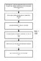
- FIG. 1is a flowchart of steps in an exemplary method 100 for fabricating semiconductor devices in accordance with the various embodiments.
- FIGS. 2A-2Dare cross-sections showing the formation of DDC devices in accordance with a particular embodiment of the method described in FIG. 1 .
- the method 100begins with the formation of a first epitaxial layer on a semiconducting substrate (step 102 ), where the first epitaxial layer includes at least one electrically active dopant.
- the dopantis added to the epitaxial process, and by forming the doped region using epitaxial growth, the likelihood of migration is reduced.
- FIG. 2A-2DA cartoon illustration for a DDC embodiment is provided at FIG. 2A-2D .
- a silicon substrate 202is provided, on which an in-situ B-doped silicon epitaxial layer (B-doped Si epi) 204 is formed.
- the surface of B-doped Si epi 204defines a new surface for the substrate 202 .
- the deposition of the B-doped Si epi 204can be preceded by an anti-punchthrough (APT) implant into the surface of substrate 202 .
- APTanti-punchthrough
- an NMOS APT implantcan be provided by implanting B at an energy of about 10 keV to 30 keV at a dose of about 5 ⁇ 10 12 atoms/cm 2 to 5 ⁇ 10 13 atoms/cm 2 .
- the B-doped Si epi 204can then be formed.
- the B-doped Si epi 204is formed by depositing a blanket layer by way of an epitaxial silicon process.
- the B dopingcan be selected to provide an appropriate doping level to define a heavily doped screen region for the P-well side of a to-be-formed device.
- a B doping concentrationbetween about 5 ⁇ 10 18 atoms/cm 3 and about 1 ⁇ 10 20 atoms/cm 3 can be provided, the particular doping concentration selected based upon desired device electrical characteristics of threshold voltage, junction leakage and other parametric considerations.
- a B-doped Si epi layer of less than 10 nmcan be formed, however, the thickness can be as high as 30 nm or more in some embodiments.
- Such a layercan be deposited using an epitaxial growth process that includes a boron doping source to provide the boron in-situ doping.
- a chemical vapor deposition (CVD) processcan be used, where B is provided by way of a suitable precursor gas, such as diborane; while disilane, silane, or dichlorosilane may be selected as the silicon precursor.
- the epitaxial growth processcan utilize processing temperatures of approximately 700C to 900C at a reduced pressure, for instance, 20 Torr.
- the exemplary embodimentsrefer primarily to the forming of silicon-comprising layers with in situ B-doping, the various embodiments are not limited in this regard.
- the first epitaxial layercan be doped in-situ with another type of electrically active dopant.
- Pcan be incorporated in-situ in a similar manner as described herein.
- FIG. 2Billustrates the application of optional additional implants for DDC NMOS devices
- FIG. 2Cillustrates the formation of doped regions for DDC PMOS devices.
- the B-doped Si epi 204is treated as an extension of the substrate 202 .
- additional implants 208can be provided as needed to set the threshold voltage (Vth) and define other characteristics for the DDC NMOS devices.
- any additional NMOS implantscan be applied via a process that includes formation of a patterned mask layer 206 to prevent dopants from being implanted into other regions of the substrate 202 , such as PMOS regions.
- the masking layer 206 shown as covering the PMOS regioncan be formed by providing a layer of photoresist which is patterned with openings to expose the regions of the substrate 202 associated with the NMOS devices.
- the processmay begin with a boron (B) anti-punchthrough implant (if not performed prior to formation of B-doped Si epi 204 ) at an energy of about 10 keV to 30 keV at a dose of about 5 ⁇ 10 12 atoms/cm 2 to 5 ⁇ 10 13 atoms/cm 2 , as well as a Boron implant at an energy of about 2 keV to 10 keV at a dose of about 1 ⁇ 10 12 atoms/cm 2 to 1 ⁇ 10 14 atoms/cm 2 .
- Bboron
- NLVtDDC NMOS low Vth
- Implant conditions discussed aboveare presented solely for purposes of illustration and not by way of limitation. In the various embodiments, more or less implants can be used. Alternatively stated, other implants, other than those described above, can be utilized as well.
- the additional dopants required for the NMOS devicescan be added during the growth of the B-doped Si epi 204 .
- the doping profile in the B-doped Si epi 204can be tailored as needed. Accordingly, the well, screen, APT, and any other regions of the NMOS devices can be formed during formation of the B-doped Si epi 204 .
- additional patterned mask layerscan be provided to apply additional implants to build out additional types of NMOS devices. For example, different sub-regions can be masked off to allow for preselected implants for the formation of NMOS standard Vth (NSVt) devices, NMOS SRAM devices in different sub-regions overlying the P-well. For each of these different device types, additional screen implants can be provided to change the Vth for each of these device types.
- NMOS analog devicescan also be formed in the P-well by using appropriate implants. The doses and energies are selected to result in a targeted concentration of dopants and depth of doped region to provide a target Vth value for these devices.
- additional Boronmay be implanted at an energy between about 2 keV to 10 keV at a dose of about 1 ⁇ 10 12 to 1 ⁇ 10 14 atoms/cm 2 .
- the various embodimentsare not limited to this particular configuration, and the implant conditions may vary as needed to meet the Vth requirements for the device design.
- the implant conditions for the additional screen implants discussedare provided solely for illustrative purposes. Any suitable set of implants can be used in the various embodiments. Further, different devices can utilize common implants. Accordingly, the masking layers can be configured during the implantation process to allow a same implant to be used for multiple device types.
- the existing blanket B-doped Si epi 204must be considered when applying such PMOS implants.
- the various embodimentsrequire higher implant doses to provide sufficient counter-doping and provide sufficient N-type doping for the PMOS device.
- the implant doseswill need to be high enough to counter the B doping in the B-doped Si epi 204 .
- the n-type implant dosewould need to be tailored to generate a peak concentration of 1.3 ⁇ 10 19 /cm 3 (8 ⁇ 10 18 /cm 3 +5 ⁇ 10 18 /cm 3 ).
- the final n-type activationwould achieve a compensated 8 ⁇ 10 18 /cm 3 n-type region.
- the P-well regions 208are effectively masked off so that the PMOS device region 212 can be formed.
- the DDC processmay begin with a phosphorous N-well implant at about 200 keV to 450 keV at a dose of about 5 ⁇ 10 12 atoms/cm 2 to 1 ⁇ 10 14 atoms/cm 2 .
- the individual devicescan include arsenic or antimony anti-punchthrough implants at an energy of about 50 keV to 200 keV at a dose of about 5 ⁇ 10 12 atoms/cm 2 to 1 ⁇ 10 14 atoms/cm 2 .
- a DDC implantfor instance, arsenic at an energy of about 2 keV to 10 keV at a dose of about 2 ⁇ 10 12 atoms/cm 2 to 2 ⁇ 10 14 atoms/cm 2 can be used to form the screen/Vt region for the DDC transistor. Variations of energies, materials and doses may apply depending on the target Vth and other specifications for the device design.
- additional patterned mask layerscan be formed to cover devices to be protected to allow for additional screening implants to be performed for the higher Vth devices which are formed using heavier concentrated regions, such as PMOS standard Vth (PSVt) values, PMOS SRAM devices, and PMOS analog devices.
- PSVtPMOS standard Vth
- additional arsenic or antimonymay be implanted at an energy of about 2 keV to 10 keV at a dose of about 2 ⁇ 10 12 atoms/cm 2 to 2 ⁇ 10 14 atoms/cm 2 .
- the doses and energiesare selected to result in a targeted concentration of dopants and depth of doped region to provide target Vth values for each type of device.
- the masking layerscan be configured during the implantation process to allow a same implant to be used for multiple device types.
- the particular implant materials and conditions provided and the mask patterns presentedare provided solely for purposes of illustration and are not intended to limit the various embodiments in any regard.
- any remaining photoresist or other mask material and any remaining sacrificial oxideshould be removed to expose the semiconducting surface including the implanted regions.
- the implanted dopantscan be activated via an anneal process (step 106 ).
- any type of anneal/activation processcan be utilized.
- the anneal processno longer requires the use of a regrowth or recrystallization anneal which requires a moderately high to high temperature over an extended period of time.
- the present disclosurecontemplates that the anneal process following the formation of the NMOS and PMOS device regions can be skipped or performed via the use of a relatively low thermal budget anneal, effective to activate any implanted species and repair any local damage caused by the ion implantation.
- the result of the foregoing processis that since the amount of B available to diffuse into the Si epi 214 is significantly reduced, the amount of migration into subsequently formed layers is also significantly reduced. Moreover, the higher-dose B implant processes (e.g., APT) are carried out at high energies, resulting in such high dose being located far from the interface between Si epi 214 and B-doped Si epi 204 . Further, any additional migration due to the defects from incompletely recrystallized portions of the substrate and due to the thermal budget for recrystallization is no longer a concern.
- APThigher-dose B implant processes
- a second epitaxial layer 214 that is undoped (that is, does not include in its process conductivity-altering dopants) or doped to a pre-determined concentrationcan be formed over the B-doped Si epi 204 on the substrate 202 (step 108 ).
- the second epitaxial layer 214can be a blanket layer formed by way of an epitaxial silicon process.
- the thickness of the second epitaxial layer 214can be selected based on desired device characteristics. For example, in one particular embodiment, a silicon epitaxial layer between 10 nm and 40 nm, such as 15 nm can be formed.
- Such a layercan be deposited using an epitaxial growth process, where the processing temperatures, the deposition time, or both are selected such that significant migration of previously implanted material is minimized.
- the epitaxial growth processcan utilize processing temperatures of approximately 600C.
- the various embodimentsare not limited in this regard. In other embodiments, depending on process conditions, device targets, and other factors, the thickness and doping levels of the second epitaxial layer 214 can vary.
- FIG. 2Dshows how shallow trench isolation (STI) features 216 can be formed after the formation of second epitaxial layer 214 .
- STIshallow trench isolation
- the STI features 216can be used not only to define separate NMOS and PMOS active areas, but additional STI features can be provided to define separate SVT, LVT, SRAM, and analog devices in the PMOS and NMOS device regions. Following the formation of these isolation features, processing of the substrate can then continue on to complete the transistor devices in the PMOS and NMOS device regions (step 112 ).
- the present disclosurecontemplates that by reducing the amount of B introduced via implantation, the amount of B interstitials and silicon interstitial/vacancy pairs available to diffuse into the Si epi 214 are reduced. However, in some embodiments, additional NMOS implants may still lead to unwanted B diffusing into the Si epi 214 . Moreover, some of the B incorporated into the B-doped Si epi 204 may still diffuse in to the Si epi 214 during anneal processes.
- a barrier material-enhanced epitaxial layeris contemplated. More specifically, the first epitaxial layer deposited on the substrate can include a barrier material incorporated therein, such as carbon, selected in amounts aimed at suppressing migration of a dopant species. Two alternative exemplary processes are described below with respect to FIGS. 3A-3D .
- FIGS. 3A-3Dshow the result of an alternate embodiment of the exemplary process flow of FIG. 1 .
- the processcan begin in a manner substantially similar to that described for FIG. 1 . That is, a substrate can be provided and a first epitaxial layer can be formed thereon, as described with respect to step 102 .
- the in-situ doped Si epiincludes both B doping and C doping to incorporate C into the B:Si epitaxial layer to inhibit migration of the boron.
- a silicon substrate 302can be provided and thereafter a B-doped C:Si epi layer 304 can be formed.
- the B dopingcan be selected to provide an appropriate doping level to define the needed doping levels for the NMOS region, including the desired concentration for screen region in the case of a DDC transistor, as previously described.
- the amount of C incorporated substitutionally into the silicon epitaxial layercan vary.
- the substitutional C concentrationcan be selected such that it is less than or equal to 1% in silicon.
- the concentration of substitutional Cmay typically be selected to be in the range of between about 1 ⁇ 10 19 atoms/cm 3 and about 1 ⁇ 10 21 atoms/cm 3 .
- the B-doped C:Si epi 304can be formed by introducing a C doping source in-situ into the B in situ-doped epitaxial process, and forming a blanket layer.
- a B-doped C:Si epi layer of less than 5 nmcan be formed, however, the thickness can be as high as 20 nm or more in some embodiments.
- Such a layercan be deposited using a single epitaxial growth process.
- a chemical vapor deposition (CVD) processcan be used, where C is provided by way of a suitable precursor gas, such as methylsilane, and B is provided by way of a suitable precursor gas, such as diborane.
- the epitaxial growth processcan utilize processing temperatures of approximately 750C.
- the result of the foregoing processis that not only are NMOS regions defined via an epitaxial deposition process rather than via implants, but subsequent B migration from the B-doped C:Si epi 304 is suppressed through the incorporation of C into the layer.
- the B dopingcan be selected such that no additional implants are needed for NMOS devices.
- the present disclosurealso contemplates that some additional B implants may be needed for some types of devices.
- additional masking and implantscan be required, as illustrated in FIG. 3B and as described above with respect to FIG. 2B . That is, a patterned masking layer 306 can be defined (and optionally a sacrificial oxide) and implants for the additional NMOS devices 308 can be applied. As shown in FIG.
- the masking layer 306can be photoresist.
- other masking layerscan be utilized as well to subdivide the device regions to form discrete additional devices of varying Vth levels by way of additional implants all performed prior to a subsequently deposited substantially undoped epitaxial Si layer.
- the PMOS region 312can be formed, as shown in FIG. 3C .
- This processcan be performed in substantially the same manner as described above with respect to FIGS. 2A-2D . That is, a patterned masking layer 310 can be defined (and optionally a sacrificial oxide) and implants for PMOS devices 312 can be applied. As shown in FIG. 3C , the masking layer 310 can be photoresist. However, as noted above, other masking layers can be utilized as well.
- the presence of the blanket B-doped C:Si epi 304will require different implant doses for the PMOS region than those previously described. Specifically, higher implant doses will be required in order to provide sufficient counter-doping to the in-situ B doping and provide sufficient N-type doping for the PMOS region. In particular embodiments, the implant doses will need to be high enough to counter the B doping in the B-doped Si epi 304 .
- the final n-type activationwould achieve a compensated 8 ⁇ 10 18 /cm 3 n-type region.
- any remaining photoresist or other mask materialshould be removed to expose the semiconducting surface including the implanted regions.
- the implanted dopantscan then be activated via an anneal process, though without a recrystallization anneal, as previously described.
- the second epitaxial layer 314 and isolation features 316can be formed, as discussed above with respect to FIGS. 2A-2D .
- a silicon comprising epitaxial layer 314can be formed, followed by formation of STI features 316 . The process can then proceed to the building of devices in the P-well 308 and N-well 312 regions.
- a further alternative processis, instead of incorporating the carbon into the in-situ doped B epitaxial process, to carry out the B in-situ doped epitaxial process first, and then follow with a C in-situ doped epitaxial process.
- An extra layer of epitaxial materialis therefore contemplated, the in-situ B doped epitaxial layer, the in-situ C doped epitaxial layer and the substantially undoped epitaxial layer formed preferably after the NMOS and PMOS device regions have been doped.
- the C concentrationis selected so that the C is effective to inhibit migration of doped species in particular, boron, while keeping the thickness of the C in-situ doped epitaxial layer to a minimum.
- the thickness of the C in-situ doped epitaxial layercan be as little as 5 nm or less, but may need to be thicker to ensure the effectiveness of the layer to inhibit diffusion.
- the substantially undoped epitaxial silicon layercan be formed.
- the C-doped regionis restricted to the bottom portion of the transistor channel.
- the substantially undoped epitaxial silicon layercan remain such and be devoid of carbon constituents.
- the final thickness of the undoped epitaxial silicon layercan be adjusted to take into account the thickness of the C doped diffusion inhibiting layer. For example, if the C doped layer were 5 nm, and the final desired thickness of the channel were 25 nm, then 20 nm of undoped epitaxial silicon can be grown over the 5 nm carbon doped layer giving rise to a 25 nm channel region free from intentional n-type or p-type dopants.
- the described process incorporating a separate C in-situ doped epitaxial layercan be used in combination with a C-doped in situ-B epitaxial layer underneath as well.
- the amount of C, B, or bothcan vary along the thickness of the B-doped C:Si epi 304 .
- the amount of C or Bcan vary along a vertical direction normal to the substrate 302 such that the amount of C, B, or both is not approximately the same along this vertical direction.
- the C-doped portioncan be restricted only to a portion of the B-doped C:Si epi 304 .
- FIG. 4is an alternate view of FIG. 3C , in which the silicon epitaxial layer is not uniform, after STI formation.
- the C comprising portion of the B-doped C:Si epi 304is restricted to the upper portion of the layer. For example, this can be the first 5-40 nm of the layer. The remaining portion of the layer can then be substantially free of C.
- B-doped C:Si epi 304is formed by first defining a B-doped portion (B-doped Si Epi 304 B) and a C comprising portion (C:Si Epi 304 A).
- B-doped Si Epi 304 BB-doped Si Epi 304 B
- C:Si Epi 304 AC comprising portion
- both portions 304 A and 304 Bcan be B-doped.
- only portion 304 Bis B-doped.
- the amount of C or B in each of these portionscan also be varied.
- the present disclosurealso contemplates that in some cases, it may be undesirable to include a C-comprising portion for certain types of devices. For instance, whereas C incorporation is important to inhibit B migration on the NMOS side, the presence of C anywhere in the PMOS region may be problematic. If it is desired to exclude C in the PMOS regions, then, after forming the blanket B-doped Si epitaxial layer and the subsequent blanket C-doped Si epitaxial layer, then the NMOS regions can be masked leaving the PMOS regions exposed, whereupon a selective etch process can be used to remove the in-situ C-doped layer from the PMOS region. This etching can be performed as follows.
- a patterned masking layercan be formed to expose the regions of C-comprising portions to be etched.
- the masking layercan consisting of a single layer of photoresist.
- the masking layercan consist of a hard mask, separately or in combination with the photoresist layer.
- Such a hard maskcan be a layer of silicon oxide, silicon nitride, or any other material which will be resistant to the removal process to be used for the epitaxial layer.
- a selective removal processis utilized to reduce the thickness of the C-comprising portions.
- the term “selective removal process”refers to any type of removal process that preferentially removes one type of material over another type of material. This can include, but is not limited to, any type of wet or dry, chemical, physical, or plasma-based etch processes for removing materials.
- the selective removal processwould be configured to preferentially remove C:Si epi over photoresist material and other masking materials.
- the specific process for the selective removal processcan vary depending on the amount of material to be removed and the amount of epitaxial layer thickness variability permitted.
- the photoresist or other masking layercan be removed to expose the surfaces of the semiconducting surface.
- This etching processcan be performed at various points in the method of FIG. 1 . In some embodiments, this process can occur prior to implants being performed (i.e., before step 104 ). In other embodiments, this process can occur after the implants, but prior to the formation of the second epitaxial layer (i.e., before step 108 ). Preferably, the selective etching of the C-containing portion should be performed prior to implanting the PMOS region with the N-type dopants. The exact point at which such a process is performed can vary depending on the desired device characteristics. Note that a further alternative to selective etching process is to use selective etching to remove B-containing layers from the PMOS side as well.
- the height of the substantially undoped epitaxial silicon layerwill vary across the surface of the substrate.
- the substantially undoped epitaxial layercan be grown and/or then polished back to maintain a substantially planar top surface.
- Another alternative technique to selectively etching the carbon doped epitaxial material from PMOS devicescould be to deposit the carbon doped epitaxial material selectively on the NMOS device regions. The in-situ doping and implant doses need to be adjusted to accommodate the expected final thickness of the substantially undoped epitaxial layer so that Vth can be set accurately. In the event that further Vth tuning is desired, channel implants or pocket implants known as “halo” following the formation of the substantially undoped epitaxial layer can be used.
Landscapes
- Engineering & Computer Science (AREA)
- Physics & Mathematics (AREA)
- Condensed Matter Physics & Semiconductors (AREA)
- General Physics & Mathematics (AREA)
- Manufacturing & Machinery (AREA)
- Computer Hardware Design (AREA)
- Microelectronics & Electronic Packaging (AREA)
- Power Engineering (AREA)
- Metal-Oxide And Bipolar Metal-Oxide Semiconductor Integrated Circuits (AREA)
- Insulated Gate Type Field-Effect Transistor (AREA)
Abstract
Description
The present invention relates to semiconductor devices and methods of fabrication thereof, and more specifically to semiconductor devices with dopant migration suppression and methods of fabrication thereof.
In certain semiconductor devices, a structure is required in which a highly doped layer is disposed adjacent to a layer with a substantially lower doping. In certain cases, this arrangement can be problematic as such structures are potentially susceptible to dopant migration, via diffusion and other mechanisms. For example, when a first layer of silicon doped with boron (B) is formed adjacent to and located underneath a second layer of silicon that is undoped or has a significantly lower B doping concentration than the first layer, unwanted migration of B into the second layer can occur when a thermal treatment is applied during fabrication of the semiconductor device. Similar results have been observed for other dopants in silicon, such as phosphorus (P) and arsenic (As). As a result, the abrupt doping transition between differentially doped layers may be degraded or compromised by subsequent thermal processing. In a worst case, the dopant could diffuse completely through the second layer, altering the undoped nature of the second layer in its entirety. In either case, the electrical characteristics of the semiconductor device can be significantly altered when dopant migration occurs.
In an effort to avoid migration of highly mobile dopants, into undoped regions, development efforts have primarily focused on: (1) reducing the thermal budget during semiconductor device manufacturing processes and (2) the implantation of additional species to form blocking regions to inhibit the migration of dopants. For example, carbon (C) implants activated into substitutional lattice sites (such as by first performing a pre-amorphization followed by C implantation and recrystallization anneal) have been utilized to suppress migration of B and P in silicon.
Both of these efforts (lower thermal budgets and migration inhibitors) have met with some success, but still have drawbacks. With respect to thermal budget reductions, at least some thermal treatments will always be required and therefore the amount of thermal budget reduction is always limited. Additionally, variations in the manufacturing process can limit the effectiveness of the reduced thermal budget. In particular, defects and interstitial/vacancy pairs generated during normal semiconductor device processing can result in migration, even when a lower thermal budget is applied. Moreover, even if thermal budgets are accurately controlled, small amounts of unwanted dopant diffusion can still have a pronounced effect on devices with reduced dimensions or devices designed with low doping concentrations. In addition, some thermal steps can simply lose effectiveness if the temperature is lowered beyond a critical minimum value.
With respect to ion implantation of a migration inhibitor such as carbon, one potential issue is that there can be inaccuracies in the placement of the carbon species, resulting in some dopants being placed in undesirable locations or atoms missing from locations where the dopant diffusion protection is needed. As a result, some migration can occur due to the ineffectiveness of the ion implantation process leading to the imperfect placement of the species intended to suppress migration. Further, ion implantation processes can introduce additional contaminating impurities into the semiconductor device and additional implant damage. Either of these can adversely affect device performance. Moreover, the extra implantation steps can introduce additional costs to the manufacturing process.
In view of the foregoing, there is a need for an alternate approach for suppressing dopant migration in semiconductor devices.
Embodiments are described with reference to the attached figures, wherein like reference numerals are used throughout the figures to designate similar or equivalent elements. The figures are not drawn to scale and they are provided merely to illustrate the embodiments. It should be understood that numerous specific details, relationships, and methods are set forth to provide a full understanding of the embodiments. One having ordinary skill in the relevant art, however, will readily recognize that embodiments can be practiced without one or more of the specific details or with other methods. In other instances, well-known structures or operations are not shown in detail to avoid obscuring the embodiments. Embodiments are not limited by the illustrated ordering of acts or events, as some acts may occur in different orders and/or concurrently with other acts or events. Furthermore, not all illustrated acts or events are required to implement a methodology in accordance with the embodiments.
As noted above, dopant migration is a significant concern in various types of semiconductor devices that include low doped (or undoped) regions abutting highly doped regions. In such devices, electrical characteristics may be dependent on the formation of a sufficiently abrupt transition of dopants between the regions. One example of such a semiconductor device is the deeply depleted channel (DDC) transistor device.
DDC transistors are formed, for example, by forming a doped region in a well for CMOS devices by forming a heavily doped screen layer (5×10¹⁸atoms/cm3to 1×10²⁰atoms/cm3). This can be followed by formation of a substantially undoped (that is, a material into which electrically modifying dopants are not purposely introduced) blanket epitaxial layer (<5×10¹⁷atoms/cm3) deposited over the screen layer, extending across multiple die and transistor die blocks.
Details regarding exemplary DDC transistor structures are more completely described in U.S. patent application Ser. No. 12/708,497 titled “ELECTRONIC DEVICES AND SYSTEMS, AND METHODS FOR MAKING AND USING THE SAME” and filed Feb. 18, 2010, U.S. patent application Ser. No. 12/971,884 titled “LOW POWER SEMICONDUCTOR TRANSISTOR STRUCTURE AND METHOD OF FABRICATION THEREOF” and filed Dec. 17, 2010, U.S. patent application Ser. No. 12/971,955 titled “TRANSISTOR WITH THRESHOLD VOLTAGE SET NOTCH AND METHOD OF FABRICATION THEREOF” and filed Dec. 17, 2010, U.S. patent application Ser. No. 12/895,785 titled “ADVANCED TRANSISTORS WITH THRESHOLD VOLTAGE SET DOPANT STRUCTURES” and filed Sep. 30, 2010, and U.S. patent application Ser. No. 12/895,813 titled “ADVANCED TRANSISTORS WITH PUNCH THROUGH SUPPRESSION” and filed Sep. 30, 2010, the disclosures of which are hereby incorporated by reference in their entirety.
Although the various embodiments will be described primarily with respect to DDC transistor devices, the various embodiments are not limited in this regard. That is, the various processes, structures and methods described herein are equally applicable to any other types of semiconductor device structures in which a highly doped region abuts a low doped or substantially undoped region, and there is the potential for migration from the doped region to the undoped region. Examples of devices designed in this manner are, super steep retrograde well devices and other depleted channel devices, or any device channel having heavily doped regions in contact with moderately doped to highly doped regions (such as traditional transistors with LDD or S/D implants adjacent to channel regions).
In depleted channel processes, the heavily doped region, which is called “well”, is typically formed via implantation of dopants. The P-well typically uses B doping. Boron migration issues are typically managed via implantation of C and careful management of thermal budget. In the case of a DDC transistor, an exemplary process flow for forming the screen regions for the DDC NMOS device can begin with B implants into the P-well for the NMOS device regions. These implants are followed by a germanium (Ge) pre-amorphization implant into the NMOS device regions at an energy of about 20 keV to 60 keV and at a dose of about 1×10¹⁴to 1×10¹⁵atoms/cm2. This Ge implant is then followed by a carbon (C) implant into the NMOS device regions at about 2 keV to 7 keV at a dose of about 1×10¹⁴atoms/cm2to 1×10¹⁵atoms/cm2. Recrystallization anneal(s) are carried out. Separately, screen implants into the N-well for the DDC PMOS device regions, for instance, Sb or As, can be applied.
After at least the DDC NMOS implants are completed, an anneal process can be performed. The anneal process serves two purposes. First, the anneal process provides for recrystallization of the portion of the substrate amorphized by the Ge implants. This recrystallization results in at least some of the implanted C being integrated into the recrystallized substrate substitutionally. The substitutional C, in turn, prevents migration of the B atoms. Second, the anneal process serves to activate the implanted dopants for the DDC device.
The DDC process flow then continues, preferably with the formation of the substantially undoped blanket epitaxial silicon, formation of isolation features, formation of transistors and other devices thereon, and formation of interconnect features.
While the process flow above does provide some suppression of B migration in DDC structures and depleted channel structures, the reliance on an ion implantation-based process has several drawbacks. First, variations in the implant processes and numerous masking steps can result in an imperfect placement of the B and C implants, and their resulting profiles in the recrystallized substrate. For example, the implanted C region may be located below the layer of the implanted B atoms, rendering the C ineffective to prevent upward migration of B.
Second, although the anneal process following Ge pre-amorphization is intended to provide recrystallization of the substrate, such a process may not provide 100% recrystallization of the amorphized and mechanically damaged portions of the substrate. As a result, any defects remaining in the substrate can create leakage paths and reduce device yield. Additionally, such defects may provide migration paths for the B and other dopants into the epitaxial silicon layer as well as providing a source of interstitials and vacancies which can result in increased dopant diffusion coefficients for a given thermal budget.
Finally, as noted above, implant processes are well-known for introducing additional impurities. Such impurities can degrade performance and consequently reduce yields.
In view of the limitations of conventional migration suppression techniques, the various embodiments described below are directed to a process flow for suppressing dopant migration for semiconductor devices that consist of substantially undoped or low doped regions formed on a highly doped substrate. In particular, a process flow in accordance with the various embodiments provides for forming at least a portion of the highly doped regions by epitaxially depositing a layer of semiconductor material on the substrate that incorporates the electrically active dopant species, that is, via in-situ doping of the semiconductor material with the dopant species of concern. For example, in the case of a depleted channel device, this process can involve depositing a layer of B-doped silicon sufficient to form the well on the NMOS device. For the DDC device, this process can include depositing a layer of B-doped silicon with sufficient dopants to form the well and screen region for DDC devices. The advantage of such a configuration is that diffusion of such dopants is limited. In general, in the case of implanted dopants, diffusion is primarily due to the presence of point defects, self-interstitials, and vacancies in the semiconductor material that enhance the diffusivity of dopants such as boron and phosphorus. These “transient enhanced diffusion (TED) mechanisms” allow dopant atoms to more easily traverse the lattice of the semiconductor material during annealing.
The practical result of in-situ doping is that since the dopants are already incorporated into the semiconductor material, an activation anneal for such dopants is not needed. Also, in-situ doping can eliminate many of the point defects that result in TED. Further, even if some additional implants of a same conductivity type are still required to tune the device characteristics, the dopants provided in-situ will be less likely to diffuse during subsequent anneal processes. Therefore, the amount of the dopant available for diffusing into an adjacent undoped or low-doped layer is reduced compared with an all-implant method for introducing dopants into the substrate. An exemplary in-situ process is described below in greater detail with respect toFIGS. 1 ,2A,2B,2C, and2D.
As shown inFIG. 1 , the method100 begins with the formation of a first epitaxial layer on a semiconducting substrate (step102), where the first epitaxial layer includes at least one electrically active dopant. The dopant is added to the epitaxial process, and by forming the doped region using epitaxial growth, the likelihood of migration is reduced. A cartoon illustration for a DDC embodiment is provided atFIG. 2A-2D . As shown inFIG. 2A , asilicon substrate 202 is provided, on which an in-situ B-doped silicon epitaxial layer (B-doped Si epi)204 is formed. The surface of B-dopedSi epi 204 defines a new surface for thesubstrate 202.
Optionally, the deposition of the B-dopedSi epi 204 can be preceded by an anti-punchthrough (APT) implant into the surface ofsubstrate 202. For example, in the case of a Si-based DDC device, an NMOS APT implant can be provided by implanting B at an energy of about 10 keV to 30 keV at a dose of about 5×10¹²atoms/cm2to 5×10¹³atoms/cm2. The B-dopedSi epi 204 can then be formed.
In one embodiment, the B-dopedSi epi 204 is formed by depositing a blanket layer by way of an epitaxial silicon process. The B doping can be selected to provide an appropriate doping level to define a heavily doped screen region for the P-well side of a to-be-formed device. In DDC embodiments, a B doping concentration between about 5×10¹⁸atoms/cm3and about 1×10²⁰atoms/cm3can be provided, the particular doping concentration selected based upon desired device electrical characteristics of threshold voltage, junction leakage and other parametric considerations. In DDC embodiments, a B-doped Si epi layer of less than 10 nm can be formed, however, the thickness can be as high as 30 nm or more in some embodiments. Such a layer can be deposited using an epitaxial growth process that includes a boron doping source to provide the boron in-situ doping. For example, in particular embodiments, a chemical vapor deposition (CVD) process can be used, where B is provided by way of a suitable precursor gas, such as diborane; while disilane, silane, or dichlorosilane may be selected as the silicon precursor. In one particular embodiment, the epitaxial growth process can utilize processing temperatures of approximately 700C to 900C at a reduced pressure, for instance, 20 Torr.
Although the exemplary embodiments refer primarily to the forming of silicon-comprising layers with in situ B-doping, the various embodiments are not limited in this regard. In other embodiments, the first epitaxial layer can be doped in-situ with another type of electrically active dopant. For example, in the case of silicon-comprising materials, P can be incorporated in-situ in a similar manner as described herein.
Referring back toFIG. 1 , once the first epitaxial layer (B-doped Si epi204) is formed, mask layers and implants can be utilized to apply any additional NMOS implants needed and to apply PMOS doped region implants, as shown inFIGS. 2B and 2C .FIG. 2B illustrates the application of optional additional implants for DDC NMOS devices andFIG. 2C illustrates the formation of doped regions for DDC PMOS devices. For purposes of describing the steps that take place after B-dopedSi epi 204 is formed, it is noted that the B-dopedSi epi 204 is treated as an extension of thesubstrate 202.
Optionally, as shown inFIG. 2B ,additional implants 208 can be provided as needed to set the threshold voltage (Vth) and define other characteristics for the DDC NMOS devices. As shown inFIG. 2B , any additional NMOS implants can be applied via a process that includes formation of a patternedmask layer 206 to prevent dopants from being implanted into other regions of thesubstrate 202, such as PMOS regions. For example, as illustrated inFIG. 2B , themasking layer 206 shown as covering the PMOS region, can be formed by providing a layer of photoresist which is patterned with openings to expose the regions of thesubstrate 202 associated with the NMOS devices. However, the various embodiments are not limited in this regard and themasking layer 206 can be formed using a hard mask layer, alone or in combination with photoresist. Such a hard mask layer can be formed using layers of silicon oxide, silicon nitride, or any other suitable hard mask layers. Optionally, a blanket sacrificial protective oxide layer (not shown) can be formed prior to the formation of themasking layer 206. Such a layer can be an in-situ steam generated (ISSG) layer or any other type of sacrificial oxide layer sufficient to protect the substrate from unwanted effects of subsequent ion implantation. Appropriate implants, such as P-type conductivity implants, are then provided according to the types of the devices to be formed.
For instance, the process may begin with a boron (B) anti-punchthrough implant (if not performed prior to formation of B-doped Si epi204) at an energy of about 10 keV to 30 keV at a dose of about 5×10¹²atoms/cm2to 5×10¹³atoms/cm2, as well as a Boron implant at an energy of about 2 keV to 10 keV at a dose of about 1×10¹²atoms/cm2to 1×10¹⁴atoms/cm2. Combined with the dopants already incorporated into the B-dopedSi epi 204, such conditions will be generally suitable for the formation of DDC NMOS low Vth (NLVt) devices. Variations in energy, material, and dose for one or more of the implants discussed above may be applied depending on the specifications from the device design. Further, the implant conditions discussed above are presented solely for purposes of illustration and not by way of limitation. In the various embodiments, more or less implants can be used. Alternatively stated, other implants, other than those described above, can be utilized as well.
In some embodiments, instead of performing such implants, the additional dopants required for the NMOS devices can be added during the growth of the B-dopedSi epi 204. For example, by varying the process conditions during growth of the B-dopedSi epi 204, such as the ratio of dopant and silicon gases during a CVD process, the doping profile in the B-dopedSi epi 204 can be tailored as needed. Accordingly, the well, screen, APT, and any other regions of the NMOS devices can be formed during formation of the B-dopedSi epi 204.
Following the completion of the implants discussed above, additional patterned mask layers can be provided to apply additional implants to build out additional types of NMOS devices. For example, different sub-regions can be masked off to allow for preselected implants for the formation of NMOS standard Vth (NSVt) devices, NMOS SRAM devices in different sub-regions overlying the P-well. For each of these different device types, additional screen implants can be provided to change the Vth for each of these device types. NMOS analog devices can also be formed in the P-well by using appropriate implants. The doses and energies are selected to result in a targeted concentration of dopants and depth of doped region to provide a target Vth value for these devices. For instance, additional Boron may be implanted at an energy between about 2 keV to 10 keV at a dose of about 1×10¹²to 1×10¹⁴atoms/cm2. However, the various embodiments are not limited to this particular configuration, and the implant conditions may vary as needed to meet the Vth requirements for the device design. The implant conditions for the additional screen implants discussed are provided solely for illustrative purposes. Any suitable set of implants can be used in the various embodiments. Further, different devices can utilize common implants. Accordingly, the masking layers can be configured during the implantation process to allow a same implant to be used for multiple device types.
Once the implants for the NMOS regions are completed, all of the NMOS devices are covered over with a mask so that the doped regions for the PMOS regions can be formed. However, in the various embodiments, the existing blanket B-dopedSi epi 204 must be considered when applying such PMOS implants. Specifically, the various embodiments require higher implant doses to provide sufficient counter-doping and provide sufficient N-type doping for the PMOS device. In particular embodiments, the implant doses will need to be high enough to counter the B doping in the B-dopedSi epi 204. For example, if the in-situ doping B concentration is 5×10¹⁸/cm3, and the final desired n-type concentration is 8×10¹⁸/cm3, then the n-type implant dose would need to be tailored to generate a peak concentration of 1.3×10¹⁹/cm3(8×1018/cm3+5×1018/cm3). In this example, the final n-type activation would achieve a compensated 8×10¹⁸/cm3n-type region.
For example, as shown inFIG. 2C , the P-well regions 208 are effectively masked off so that thePMOS device region 212 can be formed. For instance, the DDC process may begin with a phosphorous N-well implant at about 200 keV to 450 keV at a dose of about 5×10¹²atoms/cm2to 1×10¹⁴atoms/cm2. The individual devices can include arsenic or antimony anti-punchthrough implants at an energy of about 50 keV to 200 keV at a dose of about 5×10¹²atoms/cm2to 1×10¹⁴atoms/cm2. A DDC implant, for instance, arsenic at an energy of about 2 keV to 10 keV at a dose of about 2×10¹²atoms/cm2to 2×10¹⁴atoms/cm2can be used to form the screen/Vt region for the DDC transistor. Variations of energies, materials and doses may apply depending on the target Vth and other specifications for the device design.
Then, optionally, and similar to the process described above with respect toFIG. 2B , additional patterned mask layers can be formed to cover devices to be protected to allow for additional screening implants to be performed for the higher Vth devices which are formed using heavier concentrated regions, such as PMOS standard Vth (PSVt) values, PMOS SRAM devices, and PMOS analog devices. For instance, additional arsenic or antimony may be implanted at an energy of about 2 keV to 10 keV at a dose of about 2×10¹²atoms/cm2to 2×10¹⁴atoms/cm2. The doses and energies are selected to result in a targeted concentration of dopants and depth of doped region to provide target Vth values for each type of device. The masking layers can be configured during the implantation process to allow a same implant to be used for multiple device types. The particular implant materials and conditions provided and the mask patterns presented are provided solely for purposes of illustration and are not intended to limit the various embodiments in any regard.
Referring back toFIG. 1 , after the implants are completed for the devices within the P-well208 and N-well312 regions (step104), any remaining photoresist or other mask material and any remaining sacrificial oxide should be removed to expose the semiconducting surface including the implanted regions. Thereafter, the implanted dopants can be activated via an anneal process (step106).
In the various embodiments, any type of anneal/activation process can be utilized. However, what is significant regarding the various embodiments is that since the Ge amorphization implant is no longer performed, the anneal process no longer requires the use of a regrowth or recrystallization anneal which requires a moderately high to high temperature over an extended period of time. Accordingly, the present disclosure contemplates that the anneal process following the formation of the NMOS and PMOS device regions can be skipped or performed via the use of a relatively low thermal budget anneal, effective to activate any implanted species and repair any local damage caused by the ion implantation.
The result of the foregoing process is that since the amount of B available to diffuse into theSi epi 214 is significantly reduced, the amount of migration into subsequently formed layers is also significantly reduced. Moreover, the higher-dose B implant processes (e.g., APT) are carried out at high energies, resulting in such high dose being located far from the interface betweenSi epi 214 and B-dopedSi epi 204. Further, any additional migration due to the defects from incompletely recrystallized portions of the substrate and due to the thermal budget for recrystallization is no longer a concern.
Referring back toFIG. 1 , once the dopants are activated (step106), asecond epitaxial layer 214 that is undoped (that is, does not include in its process conductivity-altering dopants) or doped to a pre-determined concentration can be formed over the B-dopedSi epi 204 on the substrate202 (step108). Thesecond epitaxial layer 214 can be a blanket layer formed by way of an epitaxial silicon process. The thickness of thesecond epitaxial layer 214 can be selected based on desired device characteristics. For example, in one particular embodiment, a silicon epitaxial layer between 10 nm and 40 nm, such as 15 nm can be formed. Such a layer can be deposited using an epitaxial growth process, where the processing temperatures, the deposition time, or both are selected such that significant migration of previously implanted material is minimized. In one particular embodiment, the epitaxial growth process can utilize processing temperatures of approximately 600C. However, the various embodiments are not limited in this regard. In other embodiments, depending on process conditions, device targets, and other factors, the thickness and doping levels of thesecond epitaxial layer 214 can vary.
The present disclosure contemplates that as part of the process of forming devices in active areas or regions of the semiconducting surface, some type of active area isolation is provided. Accordingly, following the formation of the second epitaxial layer214 (step108), isolation features can be formed to define different device regions (step110). The result of this process is illustrated inFIG. 2D .FIG. 2D shows how shallow trench isolation (STI) features216 can be formed after the formation ofsecond epitaxial layer 214. However, the various embodiments are not limited to STI features and any other types of active area isolation features can be used with the various embodiments. In the various embodiments, the STI features216 can be used not only to define separate NMOS and PMOS active areas, but additional STI features can be provided to define separate SVT, LVT, SRAM, and analog devices in the PMOS and NMOS device regions. Following the formation of these isolation features, processing of the substrate can then continue on to complete the transistor devices in the PMOS and NMOS device regions (step112).
In the embodiments described above, the present disclosure contemplates that by reducing the amount of B introduced via implantation, the amount of B interstitials and silicon interstitial/vacancy pairs available to diffuse into theSi epi 214 are reduced. However, in some embodiments, additional NMOS implants may still lead to unwanted B diffusing into theSi epi 214. Moreover, some of the B incorporated into the B-dopedSi epi 204 may still diffuse in to theSi epi 214 during anneal processes.
Accordingly, in particular embodiments, a barrier material-enhanced epitaxial layer is contemplated. More specifically, the first epitaxial layer deposited on the substrate can include a barrier material incorporated therein, such as carbon, selected in amounts aimed at suppressing migration of a dopant species. Two alternative exemplary processes are described below with respect toFIGS. 3A-3D .
The amount of C incorporated substitutionally into the silicon epitaxial layer can vary. In one particular embodiment, the substitutional C concentration can be selected such that it is less than or equal to 1% in silicon. For example, the concentration of substitutional C may typically be selected to be in the range of between about 1×10¹⁹atoms/cm3and about 1×10²¹atoms/cm3. The B-doped C:Si epi 304 can be formed by introducing a C doping source in-situ into the B in situ-doped epitaxial process, and forming a blanket layer. In particular embodiments, a B-doped C:Si epi layer of less than 5 nm can be formed, however, the thickness can be as high as 20 nm or more in some embodiments. Such a layer can be deposited using a single epitaxial growth process. For example, in particular embodiments, a chemical vapor deposition (CVD) process can be used, where C is provided by way of a suitable precursor gas, such as methylsilane, and B is provided by way of a suitable precursor gas, such as diborane. In one particular embodiment, the epitaxial growth process can utilize processing temperatures of approximately 750C.
The result of the foregoing process is that not only are NMOS regions defined via an epitaxial deposition process rather than via implants, but subsequent B migration from the B-doped C:Si epi 304 is suppressed through the incorporation of C into the layer. As described above, the B doping can be selected such that no additional implants are needed for NMOS devices. However, as described above, the present disclosure also contemplates that some additional B implants may be needed for some types of devices. Thus additional masking and implants can be required, as illustrated inFIG. 3B and as described above with respect toFIG. 2B . That is, apatterned masking layer 306 can be defined (and optionally a sacrificial oxide) and implants for theadditional NMOS devices 308 can be applied. As shown inFIG. 3B , themasking layer 306 can be photoresist. However, as noted above, other masking layers can be utilized as well to subdivide the device regions to form discrete additional devices of varying Vth levels by way of additional implants all performed prior to a subsequently deposited substantially undoped epitaxial Si layer.
Once theNMOS region 308 is formed, via formation of B-doped C:Si epi 304 alone or in combination with one or more implants, thePMOS region 312 can be formed, as shown inFIG. 3C . This process can be performed in substantially the same manner as described above with respect toFIGS. 2A-2D . That is, apatterned masking layer 310 can be defined (and optionally a sacrificial oxide) and implants forPMOS devices 312 can be applied. As shown inFIG. 3C , themasking layer 310 can be photoresist. However, as noted above, other masking layers can be utilized as well.
As noted above, the presence of the blanket B-doped C:Si epi 304 will require different implant doses for the PMOS region than those previously described. Specifically, higher implant doses will be required in order to provide sufficient counter-doping to the in-situ B doping and provide sufficient N-type doping for the PMOS region. In particular embodiments, the implant doses will need to be high enough to counter the B doping in the B-dopedSi epi 304. For example, if the in-situ doping B concentration is 5×10¹⁸/cm3, and the final desired n-type concentration is 8×10¹⁸atoms/cm3, then the n-type implant dose would need to be tailored to generate a peak concentration of 1.3×10¹⁹/cm3(=8×1018+5×1018). In this example, the final n-type activation would achieve a compensated 8×10¹⁸/cm3n-type region.
After the implants are completed for thedevice regions second epitaxial layer 314 and isolation features316 can be formed, as discussed above with respect toFIGS. 2A-2D . For example, as shown inFIG. 3D , a silicon comprisingepitaxial layer 314 can be formed, followed by formation of STI features316. The process can then proceed to the building of devices in the P-well308 and N-well312 regions.
A further alternative process is, instead of incorporating the carbon into the in-situ doped B epitaxial process, to carry out the B in-situ doped epitaxial process first, and then follow with a C in-situ doped epitaxial process. An extra layer of epitaxial material is therefore contemplated, the in-situ B doped epitaxial layer, the in-situ C doped epitaxial layer and the substantially undoped epitaxial layer formed preferably after the NMOS and PMOS device regions have been doped. If a C in-situ doped epitaxial layer is used, then the C concentration is selected so that the C is effective to inhibit migration of doped species in particular, boron, while keeping the thickness of the C in-situ doped epitaxial layer to a minimum. The thickness of the C in-situ doped epitaxial layer can be as little as 5 nm or less, but may need to be thicker to ensure the effectiveness of the layer to inhibit diffusion. Following the deposition of the C in-situ doped epitaxial layer, the substantially undoped epitaxial silicon layer can be formed. Advantageously, by the process described in this embodiment, the C-doped region is restricted to the bottom portion of the transistor channel. The substantially undoped epitaxial silicon layer can remain such and be devoid of carbon constituents. In this example, the final thickness of the undoped epitaxial silicon layer can be adjusted to take into account the thickness of the C doped diffusion inhibiting layer. For example, if the C doped layer were 5 nm, and the final desired thickness of the channel were 25 nm, then 20 nm of undoped epitaxial silicon can be grown over the 5 nm carbon doped layer giving rise to a 25 nm channel region free from intentional n-type or p-type dopants. The described process incorporating a separate C in-situ doped epitaxial layer can be used in combination with a C-doped in situ-B epitaxial layer underneath as well.
The various embodiments described above contemplate that the B and C incorporated in-situ will result in a profile of B and C along a vertical direction normal to thesubstrate 302 in which the amount of C and B is approximately the same or equal throughout the thickness of the B-doped C:Si epi 304. As used herein, the terms “approximately the same” or “approximately equal” refer to the measurement being compared as having a relative difference of 10% or less. In some embodiments, the amount of C, B, or both can vary along the thickness of the B-doped C:Si epi 304. That is, the amount of C or B can vary along a vertical direction normal to thesubstrate 302 such that the amount of C, B, or both is not approximately the same along this vertical direction. For example, as shown inFIG. 4 , the C-doped portion can be restricted only to a portion of the B-doped C:Si epi 304.FIG. 4 is an alternate view ofFIG. 3C , in which the silicon epitaxial layer is not uniform, after STI formation. As shown inFIG. 4 , the C comprising portion of the B-doped C:Si epi 304 is restricted to the upper portion of the layer. For example, this can be the first 5-40 nm of the layer. The remaining portion of the layer can then be substantially free of C. Thus, B-doped C:Si epi 304 is formed by first defining a B-doped portion (B-dopedSi Epi 304B) and a C comprising portion (C:Si Epi 304A). Such a structure can be achieved during a silicon epitaxial process by separate deposition processes or via adjustment of the ratios of silicon, C, and B precursor gases and other parameters during a single deposition process. In some embodiments, bothportions only portion 304B is B-doped. Further, the amount of C or B in each of these portions can also be varied.
The present disclosure also contemplates that in some cases, it may be undesirable to include a C-comprising portion for certain types of devices. For instance, whereas C incorporation is important to inhibit B migration on the NMOS side, the presence of C anywhere in the PMOS region may be problematic. If it is desired to exclude C in the PMOS regions, then, after forming the blanket B-doped Si epitaxial layer and the subsequent blanket C-doped Si epitaxial layer, then the NMOS regions can be masked leaving the PMOS regions exposed, whereupon a selective etch process can be used to remove the in-situ C-doped layer from the PMOS region. This etching can be performed as follows. First, a patterned masking layer can be formed to expose the regions of C-comprising portions to be etched. In some embodiments, the masking layer can consisting of a single layer of photoresist. In other embodiments, the masking layer can consist of a hard mask, separately or in combination with the photoresist layer. Such a hard mask can be a layer of silicon oxide, silicon nitride, or any other material which will be resistant to the removal process to be used for the epitaxial layer.
Once the pattern is formed, a selective removal process is utilized to reduce the thickness of the C-comprising portions. As used herein, the term “selective removal process” refers to any type of removal process that preferentially removes one type of material over another type of material. This can include, but is not limited to, any type of wet or dry, chemical, physical, or plasma-based etch processes for removing materials. In the case of C:Si epi, the selective removal process would be configured to preferentially remove C:Si epi over photoresist material and other masking materials. As noted above, the specific process for the selective removal process can vary depending on the amount of material to be removed and the amount of epitaxial layer thickness variability permitted. After the selective removal process is performed, the photoresist or other masking layer can be removed to expose the surfaces of the semiconducting surface.
This etching process can be performed at various points in the method ofFIG. 1 . In some embodiments, this process can occur prior to implants being performed (i.e., before step104). In other embodiments, this process can occur after the implants, but prior to the formation of the second epitaxial layer (i.e., before step108). Preferably, the selective etching of the C-containing portion should be performed prior to implanting the PMOS region with the N-type dopants. The exact point at which such a process is performed can vary depending on the desired device characteristics. Note that a further alternative to selective etching process is to use selective etching to remove B-containing layers from the PMOS side as well. A consequence of this selective etching is that the height of the substantially undoped epitaxial silicon layer will vary across the surface of the substrate. If desired, the substantially undoped epitaxial layer can be grown and/or then polished back to maintain a substantially planar top surface. Another alternative technique to selectively etching the carbon doped epitaxial material from PMOS devices could be to deposit the carbon doped epitaxial material selectively on the NMOS device regions. The in-situ doping and implant doses need to be adjusted to accommodate the expected final thickness of the substantially undoped epitaxial layer so that Vth can be set accurately. In the event that further Vth tuning is desired, channel implants or pocket implants known as “halo” following the formation of the substantially undoped epitaxial layer can be used.
While various embodiments have been described above, it should be understood that they have been presented by way of example only, and not limitation. Numerous changes to the disclosed embodiments can be made in accordance with the disclosure herein without departing from the spirit or scope of the invention. Thus, the breadth and scope of the present invention should not be limited by any of the above described embodiments. Rather, the scope of the invention should be defined in accordance with the following claims and their equivalents.
Although the embodiments have been illustrated and described with respect to one or more implementations, equivalent alterations and modifications will occur to others skilled in the art upon the reading and understanding of this specification and the annexed drawings. In addition, while a particular feature may have been disclosed with respect to only one of several implementations, such feature may be combined with one or more other features of the other implementations as may be desired and advantageous for any given or particular application.
The terminology used herein is for the purpose of describing particular embodiments only and is not intended to be limiting of the invention. As used herein, the singular forms “a”, “an” and “the” are intended to include the plural forms as well, unless the context clearly indicates otherwise. Furthermore, to the extent that the terms “including”, “includes”, “having”, “has”, “with”, or variants thereof are used in either the detailed description and/or the claims, such terms are intended to be inclusive in a manner similar to the term “comprising.”
Unless otherwise defined, all terms (including technical and scientific terms) used herein have the same meaning as commonly understood by one of ordinary skill in the art to which this invention belongs. It will be further understood that terms, such as those defined in commonly used dictionaries, should be interpreted as having a meaning that is consistent with their meaning in the context of the relevant art and will not be interpreted in an idealized or overly formal sense unless expressly so defined herein.
Claims (19)
1. A method of fabricating a semiconductor device, comprising:
providing a substrate having a semiconducting surface;
forming a first epitaxial layer on the semiconducting surface, the first epitaxial layer comprising a first semiconducting material doped in-situ with one or more first dopants to provide a first doping concentration throughout a thickness of the first epitaxial layer corresponding to at least a doping concentration for a MOSFET well region of a first conductivity type and that is different from a doping concentration of the semiconducting surface;
adding one or more second dopants into one portion of the first epitaxial layer to define at least one counter-doped region extending through the thickness of the first epitaxial layer and having a second doping concentration corresponding to a doping concentration for a MOSFET well region of the second conductivity type and that is different from the doping concentration of the semiconducting surface; and
forming a second epitaxial layer on the first epitaxial layer, the second epitaxial layer comprising a second semiconducting material that is substantially undoped.
2. The method ofclaim 1 , wherein the step forming of the first epitaxial layer comprises incorporating at least one migration inhibiting material into the semiconducting material in situ.
3. The method ofclaim 1 , further comprising the step of forming at least one electrical isolation feature extending through at least the first epitaxial layer and the second epitaxial layer to define a plurality of regions for a plurality of devices.
4. The method ofclaim 1 , further comprising the step of forming a third epitaxial layer between the first epitaxial layer and the second epitaxial layer, the third epitaxial layer comprising semiconducting material incorporating at least one migration inhibiting material into the semiconducting material in-situ.
5. The method ofclaim 1 , further comprising:
prior to the forming of the second epitaxial layer, adding, via an ex-situ process, at least one additional dopant of the first conductivity type into at least a portion of the other regions outside the at least one counter-doped region.
6. The method ofclaim 1 , wherein the forming of the first epitaxial layer comprises selecting the first doping concentration to be substantially uniform throughout the first epitaxial layer.
7. The method ofclaim 1 , wherein the first semiconductor material and the second semiconductor material comprise silicon.
8. A method of fabricating a semiconductor device, comprising:
providing a substrate having a silicon-comprising surface;
forming a first epitaxial layer extending across the surface of the substrate, the first epitaxial layer comprising silicon-comprising material doped in-situ with one or more first dopants to provide a first doping concentration throughout a thickness of the first epitaxial layer corresponding to at least a doping concentration for a MOSFET well region of a first conductivity type and that is different from a doping concentration of the silicon-comprising surface;
implanting one or more second dopants into a portion of the first epitaxial layer to define at least one counter-doped region throughout the thickness of the first epitaxial layer having a second doping concentration corresponding to a doping concentration for a MOSFET well region of the second conductivity type and that is different from a doping concentration of the silicon-comprising surface;
forming a second epitaxial layer extending over the first epitaxial layer, the second epitaxial layer comprising substantially undoped semiconductor material; and
forming at least one isolation feature extending through at least the first epitaxial layer and the second epitaxial layer to define at least one MOSFET device area of the second conductivity type from the at least one counter-doped region and at least one MOSFET device area of the first conductivity type from other regions outside the at least one counter-doped region.
9. The method ofclaim 8 , wherein the forming of the first epitaxial layer comprises in-situ incorporation of carbon into at least one barrier portion of the first epitaxial layer.
10. The method ofclaim 9 , wherein the at least one barrier portion is disposed substantially at an interface of the first epitaxial layer and the second epitaxial region.
11. The method ofclaim 8 , wherein the at least one barrier portion is substantially free of the at least one dopant of the first conductivity type.
12. The method ofclaim 8 , wherein at least one of the first dopants comprises boron.
13. The method ofclaim 8 , further comprising:
prior to the forming of the second epitaxial layer, adding, via an ex-situ process, at least one additional dopant of the first conductivity type into at least a portion of the other regions outside the at least one counter-doped region.
14. A method of fabricating a semiconductor device, comprising:
providing a substrate having a silicon surface;
forming a first epitaxial layer on the silicon surface, the first epitaxial layer comprising silicon doped in-situ with at least boron and having a doping concentration throughout a thickness of the first epitaxial layer corresponding to a doping concentration for a P-type well region for a NFET device and that is different from a doping concentration of the silicon surface;
adding an amount of at least one N-type dopant into a portion of the substrate first epitaxial layer to define at least one counter-doped region having a doping concentration throughout the thickness of the first epitaxial layer corresponding to a doping concentration for a N-type well region for a PFET device and that is different from the doping concentration of the silicon surface;
forming a second epitaxial layer on the first epitaxial layer, the second epitaxial layer comprising substantially undoped silicon; and
forming at least one isolation feature extending through at least the first epitaxial layer and the second epitaxial layer to define at least one PFET device region in the at least one counter-doped region and at least one NFET device region outside the at least one counter-doped region.
15. The method ofclaim 14 , wherein the forming of the first epitaxial layer comprises in-situ incorporation of carbon into at least one barrier portion of the first epitaxial layer.
16. The method ofclaim 15 , wherein the at least one barrier portion is disposed substantially at an interface of the first epitaxial layer and the second epitaxial region.
17. The method ofclaim 15 , wherein the at least one barrier portion is substantially free of boron.
18. The method ofclaim 14 , further comprising:
prior to the forming of the second epitaxial layer, adding, via an ex-situ process, at least one additional P-type dopant into at least a portion of the other regions outside the at least one counter-doped region.
19. The method ofclaim 14 , wherein the forming of the first epitaxial layer comprises selecting an amount of the boron to be approximately the same throughout the first epitaxial layer in a direction normal to the silicon surface.
Priority Applications (1)
| Application Number | Priority Date | Filing Date | Title |
|---|---|---|---|
| US13/622,194US9112057B1 (en) | 2012-09-18 | 2012-09-18 | Semiconductor devices with dopant migration suppression and method of fabrication thereof |
Applications Claiming Priority (1)
| Application Number | Priority Date | Filing Date | Title |
|---|---|---|---|
| US13/622,194US9112057B1 (en) | 2012-09-18 | 2012-09-18 | Semiconductor devices with dopant migration suppression and method of fabrication thereof |
Publications (1)
| Publication Number | Publication Date |
|---|---|
| US9112057B1true US9112057B1 (en) | 2015-08-18 |
Family
ID=53786109
Family Applications (1)
| Application Number | Title | Priority Date | Filing Date |
|---|---|---|---|
| US13/622,194Active2033-01-05US9112057B1 (en) | 2012-09-18 | 2012-09-18 | Semiconductor devices with dopant migration suppression and method of fabrication thereof |
Country Status (1)
| Country | Link |
|---|---|
| US (1) | US9112057B1 (en) |
Cited By (5)
| Publication number | Priority date | Publication date | Assignee | Title |
|---|---|---|---|---|
| US20140252504A1 (en)* | 2013-03-11 | 2014-09-11 | Taiwan Semiconductor Manufacturing Company, Ltd. | Method for Fabricating a Semiconductor Device |
| US20150137247A1 (en)* | 2013-11-15 | 2015-05-21 | Taiwan Semiconductor Manufacturing Company Ltd. | Semiconductor device and manufacturing method thereof |
| US20150294865A1 (en)* | 2014-04-14 | 2015-10-15 | Taiwan Semiconductor Manufacturing Company, Ltd. | Semiconductor devices and methods for manufacturing the same |
| US9478642B2 (en)* | 2014-11-10 | 2016-10-25 | Globalfoundries Inc. | Semiconductor junction formation |
| US9608069B1 (en) | 2016-04-13 | 2017-03-28 | Intenational Business Machines Corporation | Self aligned epitaxial based punch through control |
Citations (475)
| Publication number | Priority date | Publication date | Assignee | Title |
|---|---|---|---|---|
| US3958266A (en) | 1974-04-19 | 1976-05-18 | Rca Corporation | Deep depletion insulated gate field effect transistors |
| US4000504A (en) | 1975-05-12 | 1976-12-28 | Hewlett-Packard Company | Deep channel MOS transistor |
| US4021835A (en) | 1974-01-25 | 1977-05-03 | Hitachi, Ltd. | Semiconductor device and a method for fabricating the same |
| US4242691A (en) | 1978-09-18 | 1980-12-30 | Mitsubishi Denki Kabushiki Kaisha | MOS Semiconductor device |
| US4276095A (en) | 1977-08-31 | 1981-06-30 | International Business Machines Corporation | Method of making a MOSFET device with reduced sensitivity of threshold voltage to source to substrate voltage variations |
| US4315781A (en) | 1980-04-23 | 1982-02-16 | Hughes Aircraft Company | Method of controlling MOSFET threshold voltage with self-aligned channel stop |
| JPS59193066U (en) | 1983-06-08 | 1984-12-21 | 三菱電機株式会社 | Elevator security TV camera |
| US4518926A (en) | 1982-12-20 | 1985-05-21 | At&T Bell Laboratories | Gate-coupled field-effect transistor pair amplifier |
| US4559091A (en) | 1984-06-15 | 1985-12-17 | Regents Of The University Of California | Method for producing hyperabrupt doping profiles in semiconductors |
| US4578128A (en) | 1984-12-03 | 1986-03-25 | Ncr Corporation | Process for forming retrograde dopant distributions utilizing simultaneous outdiffusion of dopants |
| US4617066A (en) | 1984-11-26 | 1986-10-14 | Hughes Aircraft Company | Process of making semiconductors having shallow, hyperabrupt doped regions by implantation and two step annealing |
| US4662061A (en) | 1985-02-27 | 1987-05-05 | Texas Instruments Incorporated | Method for fabricating a CMOS well structure |
| US4761384A (en) | 1986-06-10 | 1988-08-02 | Siemens Aktiengesellschaft | Forming retrograde twin wells by outdiffusion of impurity ions in epitaxial layer followed by CMOS device processing |
| US4780748A (en) | 1986-06-06 | 1988-10-25 | American Telephone & Telegraph Company, At&T Bell Laboratories | Field-effect transistor having a delta-doped ohmic contact |
| US4819043A (en) | 1985-11-29 | 1989-04-04 | Hitachi, Ltd. | MOSFET with reduced short channel effect |
| EP0312237A2 (en) | 1987-10-13 | 1989-04-19 | AT&T Corp. | Interface charge enhancement in delta-doped heterostructure |
| US4885477A (en) | 1987-06-08 | 1989-12-05 | U.S. Philips Corporation | Differential amplifier and current sensing circuit including such an amplifier |
| US4908681A (en) | 1980-04-30 | 1990-03-13 | Sanyo Electric Co., Ltd. | Insulated gate field effect transistor with buried layer |
| US4945254A (en) | 1986-03-19 | 1990-07-31 | The Secretary of State for Defence in Her Britannic Majesty's Government for the United Kingdom of Great Britain and Northern Ireland | Method and apparatus for monitoring surface layer growth |
| US4956311A (en) | 1989-06-27 | 1990-09-11 | National Semiconductor Corporation | Double-diffused drain CMOS process using a counterdoping technique |
| US5034337A (en) | 1989-02-10 | 1991-07-23 | Texas Instruments Incorporated | Method of making an integrated circuit that combines multi-epitaxial power transistors with logic/analog devices |
| US5144378A (en) | 1990-03-06 | 1992-09-01 | Fujitsu Limited | High electron mobility transistor |
| US5156989A (en) | 1988-11-08 | 1992-10-20 | Siliconix, Incorporated | Complementary, isolated DMOS IC technology |
| US5156990A (en) | 1986-07-23 | 1992-10-20 | Texas Instruments Incorporated | Floating-gate memory cell with tailored doping profile |
| US5166765A (en) | 1991-08-26 | 1992-11-24 | At&T Bell Laboratories | Insulated gate field-effect transistor with pulse-shaped doping |
| US5208473A (en) | 1989-11-29 | 1993-05-04 | Mitsubishi Denki Kabushiki Kaisha | Lightly doped MISFET with reduced latchup and punchthrough |
| US5294821A (en) | 1990-10-09 | 1994-03-15 | Seiko Epson Corporation | Thin-film SOI semiconductor device having heavily doped diffusion regions beneath the channels of transistors |
| US5298763A (en) | 1992-11-02 | 1994-03-29 | Motorola, Inc. | Intrinsically doped semiconductor structure and method for making |
| EP0274278B1 (en) | 1987-01-05 | 1994-05-25 | Seiko Instruments Inc. | MOS field effect transistor and method of manufacturing the same |
| US5369288A (en) | 1992-05-08 | 1994-11-29 | Fujitsu Limited | Semiconductor device for switching a ballistic flow of carriers |
| US5373186A (en) | 1984-11-19 | 1994-12-13 | Max-Planck Gesellschaft Zur Foerderung Der Wissenschaften E.V. | Bipolar transistor with monoatomic base layer between emitter and collector layers |
| US5384476A (en) | 1979-08-25 | 1995-01-24 | Zaidan Hojin Handotai Kenkyu Shinkokai | Short channel MOSFET with buried anti-punch through region |
| US5426328A (en) | 1992-09-21 | 1995-06-20 | Siliconix Incorporated | BICDMOS structures |
| US5444008A (en) | 1993-09-24 | 1995-08-22 | Vlsi Technology, Inc. | High-performance punchthrough implant method for MOS/VLSI |
| EP0531621A3 (en) | 1991-09-12 | 1995-08-30 | Po Hang Iron & Steel | Process for formation of delta-doped quantum well field effect transistor |
| US5552332A (en) | 1995-06-02 | 1996-09-03 | Motorola, Inc. | Process for fabricating a MOSFET device having reduced reverse short channel effects |
| US5559368A (en) | 1994-08-30 | 1996-09-24 | The Regents Of The University Of California | Dynamic threshold voltage mosfet having gate to body connection for ultra-low voltage operation |
| US5608253A (en) | 1995-03-22 | 1997-03-04 | Advanced Micro Devices Inc. | Advanced transistor structures with optimum short channel controls for high density/high performance integrated circuits |
| US5622880A (en) | 1994-08-18 | 1997-04-22 | Sun Microsystems, Inc. | Method of making a low power, high performance junction transistor |
| US5624863A (en) | 1995-07-17 | 1997-04-29 | Micron Technology, Inc. | Semiconductor processing method of forming complementary N-type doped and P-type doped active regions within a semiconductor substrate |
| US5625568A (en) | 1993-12-22 | 1997-04-29 | Vlsi Technology, Inc. | Method and apparatus for compacting integrated circuits with standard cell architectures |
| US5641980A (en) | 1995-06-16 | 1997-06-24 | Mitsubishi Denki Kabushiki Kaisha | Device having a high concentration region under the channel |
| US5663583A (en) | 1995-06-06 | 1997-09-02 | Hughes Aircraft Company | Low-noise and power ALGaPSb/GaInAs HEMTs and pseudomorpohic HEMTs on GaAs substrate |
| US5712501A (en) | 1995-10-10 | 1998-01-27 | Motorola, Inc. | Graded-channel semiconductor device |
| US5726562A (en) | 1995-09-07 | 1998-03-10 | Nec Corporation | Semiconductor device and power supply controller for same |
| US5726488A (en) | 1985-11-29 | 1998-03-10 | Hitachi, Ltd. | Semiconductor device having semiconductor elements formed in a retrograde well structure |
| US5731626A (en) | 1994-12-01 | 1998-03-24 | Lucent Technologies Inc. | Process for controlling dopant diffusion in a semiconductor layer and semiconductor layer formed thereby |
| US5736419A (en) | 1996-11-12 | 1998-04-07 | National Semiconductor Corporation | Method of fabricating a raised source/drain MOSFET using self-aligned POCl3 for doping gate/source/drain regions |
| US5753555A (en) | 1995-11-22 | 1998-05-19 | Nec Corporation | Method for forming semiconductor device |
| US5754826A (en) | 1995-08-04 | 1998-05-19 | Synopsys, Inc. | CAD and simulation system for targeting IC designs to multiple fabrication processes |
| US5756365A (en) | 1992-10-30 | 1998-05-26 | Kabushiki Kaisha Toshiba | Method of manufacturing MOS-type semiconductor device having electrode structure capable of coping with short-channel effects |
| US5763921A (en) | 1991-10-22 | 1998-06-09 | Mitsubishi Denki Kabushiki Kaisha | Semiconductor device including retrograde well structure with suppressed substrate bias effects |
| US5847419A (en) | 1996-09-17 | 1998-12-08 | Kabushiki Kaisha Toshiba | Si-SiGe semiconductor device and method of fabricating the same |
| US5856003A (en) | 1997-11-17 | 1999-01-05 | Taiwan Semiconductor Manufacturing Company, Ltd. | Method for forming pseudo buried layer for sub-micron bipolar or BiCMOS device |
| US5861334A (en) | 1995-08-07 | 1999-01-19 | Hyundai Electronics Industries Co., | Method for fabricating semiconductor device having a buried channel |
| US5885876A (en) | 1996-02-07 | 1999-03-23 | Thunderbird Technologies, Inc. | Methods of fabricating short channel fermi-threshold field effect transistors including drain field termination region |
| US5889315A (en) | 1994-08-18 | 1999-03-30 | National Semiconductor Corporation | Semiconductor structure having two levels of buried regions |
| US5895954A (en) | 1997-03-27 | 1999-04-20 | Mitsubishi Denki Kabushiki Kaisha | Field effect transistor with impurity concentration peak under gate electrode |
| US5918129A (en) | 1997-02-25 | 1999-06-29 | Advanced Micro Devices, Inc. | Method of channel doping using diffusion from implanted polysilicon |
| US5923067A (en) | 1997-04-04 | 1999-07-13 | International Business Machines Corporation | 3-D CMOS-on-SOI ESD structure and method |
| US5923987A (en) | 1997-06-30 | 1999-07-13 | Sun Microsystems, Inc. | Method for forming MOS devices with retrograde pocket regions and counter dopant regions at the substrate surface |
| US5936868A (en) | 1997-03-06 | 1999-08-10 | Harris Corporation | Method for converting an integrated circuit design for an upgraded process |
| US5946214A (en) | 1997-07-11 | 1999-08-31 | Advanced Micro Devices | Computer implemented method for estimating fabrication yield for semiconductor integrated circuit including memory blocks with redundant rows and/or columns |
| US5985705A (en) | 1998-06-30 | 1999-11-16 | Lsi Logic Corporation | Low threshold voltage MOS transistor and method of manufacture |
| US5989963A (en) | 1997-07-21 | 1999-11-23 | Advanced Micro Devices, Inc. | Method for obtaining a steep retrograde channel profile |
| US6001695A (en) | 1998-03-02 | 1999-12-14 | Texas Instruments - Acer Incorporated | Method to form ultra-short channel MOSFET with a gate-side airgap structure |
| US6020227A (en) | 1995-09-12 | 2000-02-01 | National Semiconductor Corporation | Fabrication of multiple field-effect transistor structure having local threshold-adjust doping |
| US6060345A (en) | 1997-04-21 | 2000-05-09 | Advanced Micro Devices, Inc. | Method of making NMOS and PMOS devices with reduced masking steps |
| US6060364A (en) | 1999-03-02 | 2000-05-09 | Advanced Micro Devices, Inc. | Fast Mosfet with low-doped source/drain |
| US6066533A (en) | 1998-09-29 | 2000-05-23 | Advanced Micro Devices, Inc. | MOS transistor with dual metal gate structure |
| US6072217A (en) | 1998-06-11 | 2000-06-06 | Sun Microsystems, Inc. | Tunable threshold SOI device using isolated well structure for back gate |
| US6087210A (en) | 1998-06-05 | 2000-07-11 | Hyundai Electronics Industries | Method of manufacturing a CMOS Transistor |
| US6087691A (en) | 1997-02-04 | 2000-07-11 | Mitsubishi Denki Kabushiki Kaisha | Semiconductor device having lower minority carrier noise |
| US6088518A (en) | 1998-01-30 | 2000-07-11 | Aspec Technology, Inc. | Method and system for porting an integrated circuit layout from a reference process to a target process |
| US6091286A (en) | 1994-02-14 | 2000-07-18 | Philips Electronics North America Corporation | Fully integrated reference circuit having controlled temperature dependence |
| US6096611A (en) | 1998-03-13 | 2000-08-01 | Texas Instruments - Acer Incorporated | Method to fabricate dual threshold CMOS circuits |
| US6103562A (en) | 1998-01-14 | 2000-08-15 | Lg Semicon Co., Ltd. | Method of making semiconductor device with decreased channel width and constant threshold voltage |
| US6121153A (en) | 1994-08-29 | 2000-09-19 | Fujitsu Limited | Semiconductor device having a regrowth crystal region |
| US6147383A (en) | 1995-03-10 | 2000-11-14 | Sony Corporation | LDD buried channel field effect semiconductor device and manufacturing method |
| US6153920A (en) | 1994-12-01 | 2000-11-28 | Lucent Technologies Inc. | Process for controlling dopant diffusion in a semiconductor layer and semiconductor device formed thereby |
| US6157073A (en) | 1997-09-29 | 2000-12-05 | Stmicroelectronics S.A. | Isolation between power supplies of an analog-digital circuit |
| US6175582B1 (en) | 1997-11-26 | 2001-01-16 | Mitsui Chemicals Inc. | Semiconductor laser device |
| US6184112B1 (en) | 1998-12-02 | 2001-02-06 | Advanced Micro Devices, Inc. | Method of forming a MOSFET transistor with a shallow abrupt retrograde dopant profile |
| US6190979B1 (en) | 1999-07-12 | 2001-02-20 | International Business Machines Corporation | Method for fabricating dual workfunction devices on a semiconductor substrate using counter-doping and gapfill |
| US6194259B1 (en) | 1997-06-27 | 2001-02-27 | Advanced Micro Devices, Inc. | Forming retrograde channel profile and shallow LLDD/S-D extensions using nitrogen implants |
| US6198157B1 (en) | 1997-02-26 | 2001-03-06 | Hitachi, Ltd. | Semiconductor device having buried boron and carbon regions |
| US6218895B1 (en) | 1997-06-20 | 2001-04-17 | Intel Corporation | Multiple well transistor circuits having forward body bias |
| US6218892B1 (en) | 1997-06-20 | 2001-04-17 | Intel Corporation | Differential circuits employing forward body bias |
| US6221724B1 (en) | 1998-11-06 | 2001-04-24 | Advanced Micro Devices, Inc. | Method of fabricating an integrated circuit having punch-through suppression |
| US6232164B1 (en) | 1999-05-24 | 2001-05-15 | Taiwan Semiconductor Manufacturing Company | Process of making CMOS device structure having an anti-SCE block implant |
| US6235597B1 (en) | 1999-08-06 | 2001-05-22 | International Business Machines Corporation | Semiconductor structure having reduced silicide resistance between closely spaced gates and method of fabrication |
| US6245618B1 (en) | 1999-02-03 | 2001-06-12 | Advanced Micro Devices, Inc. | Mosfet with localized amorphous region with retrograde implantation |
| US6268640B1 (en) | 1999-08-12 | 2001-07-31 | International Business Machines Corporation | Forming steep lateral doping distribution at source/drain junctions |
| US6271070B2 (en) | 1997-12-25 | 2001-08-07 | Matsushita Electronics Corporation | Method of manufacturing semiconductor device |
| US6271551B1 (en) | 1995-12-15 | 2001-08-07 | U.S. Philips Corporation | Si-Ge CMOS semiconductor device |
| EP0683515B1 (en) | 1994-05-17 | 2001-08-16 | Samsung Electronics Co., Ltd. | Method of manufacturing a CMOS device |
| US20010014495A1 (en) | 1999-01-27 | 2001-08-16 | Bin Yu | Method for forming super-steep retrograded channel (SSRC) for cmos transistor using rapid laser annealing to reduce thermal budget |
| US6288429B1 (en) | 1996-12-04 | 2001-09-11 | Sharp Kabushiki Kaisha | Semiconductor device |
| US6297132B1 (en) | 2000-02-07 | 2001-10-02 | Chartered Semiconductor Manufacturing Ltd. | Process to control the lateral doping profile of an implanted channel region |
| US6300177B1 (en) | 2001-01-25 | 2001-10-09 | Chartered Semiconductor Manufacturing Inc. | Method to form transistors with multiple threshold voltages (VT) using a combination of different work function gate materials |
| US6300209B1 (en)* | 1999-06-24 | 2001-10-09 | Hyundai Electronics Industries Co., Ltd. | Method of fabricating triple well of semiconductor device using SEG |
| US6313489B1 (en) | 1999-11-16 | 2001-11-06 | Philips Electronics North America Corporation | Lateral thin-film silicon-on-insulator (SOI) device having a lateral drift region with a retrograde doping profile, and method of making such a device |
| US6320222B1 (en) | 1998-09-01 | 2001-11-20 | Micron Technology, Inc. | Structure and method for reducing threshold voltage variations due to dopant fluctuations |
| US6319799B1 (en) | 2000-05-09 | 2001-11-20 | Board Of Regents, The University Of Texas System | High mobility heterojunction transistor and method |
| US6323525B1 (en) | 1997-09-18 | 2001-11-27 | Kabushiki Kaisha Toshiba | MISFET semiconductor device having relative impurity concentration levels between layers |
| US6326666B1 (en) | 2000-03-23 | 2001-12-04 | International Business Machines Corporation | DTCMOS circuit having improved speed |
| US6335233B1 (en) | 1998-07-02 | 2002-01-01 | Samsung Electronics Co., Ltd. | Method for fabricating MOS transistor |
| US6358806B1 (en) | 2001-06-29 | 2002-03-19 | Lsi Logic Corporation | Silicon carbide CMOS channel |
| US20020033511A1 (en) | 2000-09-15 | 2002-03-21 | Babcock Jeffrey A. | Advanced CMOS using super steep retrograde wells |
| US20020042184A1 (en) | 2000-10-10 | 2002-04-11 | Mahalingam Nandakumar | Reduction in well implant channeling and resulting latchup characteristics in shallow trench ilolation by implanting wells through nitride |
| US6380019B1 (en) | 1998-11-06 | 2002-04-30 | Advanced Micro Devices, Inc. | Method of manufacturing a transistor with local insulator structure |
| US6391752B1 (en) | 2000-09-12 | 2002-05-21 | Taiwan Semiconductor Manufacturing, Co., Ltd. | Method of fabricating a silicon-on-insulator semiconductor device with an implanted ground plane |
| US6426279B1 (en) | 1999-08-18 | 2002-07-30 | Advanced Micro Devices, Inc. | Epitaxial delta doping for retrograde channel profile |
| US6426260B1 (en) | 1997-12-02 | 2002-07-30 | Magepower Semiconductor Corp. | Switching speed improvement in DMO by implanting lightly doped region under gate |
| US6432754B1 (en) | 2001-02-20 | 2002-08-13 | International Business Machines Corporation | Double SOI device with recess etch and epitaxy |
| US6444551B1 (en) | 2001-07-23 | 2002-09-03 | Taiwan Semiconductor Manufacturing Company | N-type buried layer drive-in recipe to reduce pits over buried antimony layer |
| US6444550B1 (en) | 1999-08-18 | 2002-09-03 | Advanced Micro Devices, Inc. | Laser tailoring retrograde channel profile in surfaces |
| US6449749B1 (en) | 1999-11-18 | 2002-09-10 | Pdf Solutions, Inc. | System and method for product yield prediction |
| US6461928B2 (en) | 2000-05-23 | 2002-10-08 | Texas Instruments Incorporated | Methodology for high-performance, high reliability input/output devices and analog-compatible input/output and core devices using core device implants |
| US6461920B1 (en) | 1996-04-01 | 2002-10-08 | Mitsubishi Denki Kabushiki Kaisha | Semiconductor device and method of manufacturing the same |
| US20020151153A1 (en)* | 2001-04-11 | 2002-10-17 | Texas Instruments Incorporated | Carbon doped epitaxial layer for high speed CB-CMOS |
| US6472278B1 (en) | 1998-06-22 | 2002-10-29 | Motorola, Inc. | Method and apparatus for creating a voltage threshold in a FET |
| US6482714B1 (en) | 1999-02-24 | 2002-11-19 | Kabushiki Kaisha Toshiba | Semiconductor device and method of manufacturing the same |
| US6489224B1 (en) | 2001-05-31 | 2002-12-03 | Sun Microsystems, Inc. | Method for engineering the threshold voltage of a device using buried wells |
| US6492232B1 (en) | 1998-06-15 | 2002-12-10 | Motorola, Inc. | Method of manufacturing vertical semiconductor device |
| US6500739B1 (en) | 2001-06-14 | 2002-12-31 | Taiwan Semiconductor Manufacturing Company | Formation of an indium retrograde profile via antimony ion implantation to improve NMOS short channel effect |
| US6503801B1 (en) | 1999-08-18 | 2003-01-07 | Advanced Micro Devices, Inc. | Non-uniform channel profile via enhanced diffusion |
| US6503805B2 (en) | 1999-09-02 | 2003-01-07 | Micron Technology, Inc. | Channel implant through gate polysilicon |
| US20030006415A1 (en) | 2000-06-27 | 2003-01-09 | Toshiya Yokogawa | Semiconductor device |
| US6506640B1 (en) | 1999-09-24 | 2003-01-14 | Advanced Micro Devices, Inc. | Multiple channel implantation to form retrograde channel profile and to engineer threshold voltage and sub-surface punch-through |
| US6518623B1 (en) | 2000-06-09 | 2003-02-11 | Mitsubishi Denki Kabushiki Kaisha | Semiconductor device having a buried-channel MOS structure |
| US6521470B1 (en) | 2001-10-31 | 2003-02-18 | United Microelectronics Corp. | Method of measuring thickness of epitaxial layer |
| US6534373B1 (en) | 2001-03-26 | 2003-03-18 | Advanced Micro Devices, Inc. | MOS transistor with reduced floating body effect |
| US6541829B2 (en) | 1999-12-03 | 2003-04-01 | Kabushiki Kaisha Toshiba | Semiconductor device and method of manufacturing the same |
| US6541328B2 (en) | 2001-02-19 | 2003-04-01 | Samsung Electronics Co., Ltd. | Method of fabricating metal oxide semiconductor transistor with lightly doped impurity regions formed after removing spacers used for defining higher density impurity regions |
| US6548842B1 (en) | 2000-03-31 | 2003-04-15 | National Semiconductor Corporation | Field-effect transistor for alleviating short-channel effects |
| US6551885B1 (en) | 2001-02-09 | 2003-04-22 | Advanced Micro Devices, Inc. | Low temperature process for a thin film transistor |
| US6573129B2 (en) | 1999-08-06 | 2003-06-03 | Raytheon Company | Gate electrode formation in double-recessed transistor by two-step etching |
| US6600200B1 (en) | 1999-08-25 | 2003-07-29 | Infineon Technologies Ag | MOS transistor, method for fabricating a MOS transistor and method for fabricating two complementary MOS transistors |
| US6620671B1 (en) | 2001-05-01 | 2003-09-16 | Advanced Micro Devices, Inc. | Method of fabricating transistor having a single crystalline gate conductor |
| US20030173626A1 (en) | 2001-05-18 | 2003-09-18 | Burr James B. | Device including a resistive path to introduce an equivalent RC circuit |
| US6624488B1 (en) | 2000-08-07 | 2003-09-23 | Advanced Micro Devices, Inc. | Epitaxial silicon growth and usage of epitaxial gate insulator for low power, high performance devices |
| US6627473B1 (en) | 1999-11-16 | 2003-09-30 | Nec Compound Semiconductor Devices, Ltd. | Compound semiconductor device with delta doped layer under etching stopper layer for decreasing resistance between active layer and ohmic electrode and process of fabrication thereof |
| US20030183856A1 (en) | 2002-03-28 | 2003-10-02 | Karsten Wieczorek | Semiconductor device having a retrograde dopant profile in a channel region and method for fabricating the same |
| US6630710B1 (en) | 1998-09-29 | 2003-10-07 | Newport Fab, Llc | Elevated channel MOSFET |
| US20030215992A1 (en) | 2002-05-20 | 2003-11-20 | Sohn Yong Sun | Method for forming transistor of semiconductor device |
| US6660605B1 (en) | 2002-11-12 | 2003-12-09 | Texas Instruments Incorporated | Method to fabricate optimal HDD with dual diffusion process to optimize transistor drive current junction capacitance, tunneling current and channel dopant loss |
| US6662350B2 (en) | 2002-01-28 | 2003-12-09 | International Business Machines Corporation | FinFET layout generation |
| US6670260B1 (en) | 1998-11-06 | 2003-12-30 | Advanced Micro Devices, Inc. | Transistor with local insulator structure |
| US6693333B1 (en) | 2001-05-01 | 2004-02-17 | Advanced Micro Devices, Inc. | Semiconductor-on-insulator circuit with multiple work functions |
| US20040051104A1 (en)* | 2001-09-14 | 2004-03-18 | Kenya Yamashita | Semiconductor device |
| US20040053457A1 (en) | 2002-09-17 | 2004-03-18 | Yong-Sun Sohn | Method for fabricating semiconductor device with ultra-shallow super-steep-retrograde epi-channel by boron-fluoride compound doping |
| JP2004087671A (en) | 2002-08-26 | 2004-03-18 | Sharp Corp | Semiconductor device and method of manufacturing the same |
| US20040075143A1 (en) | 2000-01-07 | 2004-04-22 | Geum-Jong Bae | CMOS integrated circuit devices and substrates having buried silicon germanium layers therein and methods of forming same |
| US20040075118A1 (en) | 2000-12-08 | 2004-04-22 | Bernd Heinemann | Layers in substrate wafers |
| US20040084731A1 (en) | 2001-03-29 | 2004-05-06 | Kabushiki Kaisha Toshiba | Semiconductor device comprising buried channel region and method for manufacturing the same |
| US20040087090A1 (en) | 2002-10-31 | 2004-05-06 | Grudowski Paul A. | Semiconductor fabrication process using transistor spacers of differing widths |
| US6743684B2 (en) | 2002-10-11 | 2004-06-01 | Texas Instruments Incorporated | Method to produce localized halo for MOS transistor |
| US6743291B2 (en) | 2002-07-09 | 2004-06-01 | Chartered Semiconductor Manufacturing Ltd. | Method of fabricating a CMOS device with integrated super-steep retrograde twin wells using double selective epitaxial growth |
| US6751519B1 (en) | 2001-10-25 | 2004-06-15 | Kla-Tencor Technologies Corporation | Methods and systems for predicting IC chip yield |
| US6753230B2 (en) | 2002-05-18 | 2004-06-22 | Hynix Semiconductor Inc. | Method for fabricating semiconductor device with ultra-shallow super-steep-retrograde epi-channel by decaborane doping |
| US20040126947A1 (en) | 2002-12-30 | 2004-07-01 | Hynix Semiconductor Inc. | pMOS device having ultra shallow super-steep-retrograde epi-channel with dual channel doping and method for fabricating the same |
| US6760900B2 (en) | 2001-12-03 | 2004-07-06 | Anadigics Inc. | Integrated circuits with scalable design |
| US6787424B1 (en) | 2001-02-09 | 2004-09-07 | Advanced Micro Devices, Inc. | Fully depleted SOI transistor with elevated source and drain |
| US20040175893A1 (en) | 2003-03-07 | 2004-09-09 | Applied Materials, Inc. | Apparatuses and methods for forming a substantially facet-free epitaxial film |
| US20040180488A1 (en) | 2003-03-13 | 2004-09-16 | Won-Ho Lee | Method for fabricating complementary metal oxide semiconductor image sensor |
| US6797602B1 (en) | 2001-02-09 | 2004-09-28 | Advanced Micro Devices, Inc. | Method of manufacturing a semiconductor device with supersaturated source/drain extensions and metal silicide contacts |
| US6797994B1 (en) | 2000-02-14 | 2004-09-28 | Raytheon Company | Double recessed transistor |
| US6797553B2 (en) | 2000-10-24 | 2004-09-28 | International Business Machines Corporation | Method for making multiple threshold voltage FET using multiple work-function gate materials |
| US6808004B2 (en) | 2002-01-31 | 2004-10-26 | Tht Presses Inc. | Semi-solid molding method |
| US6808994B1 (en) | 2003-06-17 | 2004-10-26 | Micron Technology, Inc. | Transistor structures and processes for forming same |
| US6813750B2 (en) | 2001-04-02 | 2004-11-02 | Kabushiki Kaisha Toshiba | Logic circuit design equipment and method for designing logic circuit for reducing leakage current |
| US6822297B2 (en) | 2001-06-07 | 2004-11-23 | Texas Instruments Incorporated | Additional n-type LDD/pocket implant for improving short-channel NMOS ESD robustness |
| US6821852B2 (en) | 2001-02-13 | 2004-11-23 | Micron Technology, Inc. | Dual doped gates |
| US6821825B2 (en) | 2001-02-12 | 2004-11-23 | Asm America, Inc. | Process for deposition of semiconductor films |
| US6831292B2 (en) | 2001-09-21 | 2004-12-14 | Amberwave Systems Corporation | Semiconductor structures employing strained material layers with defined impurity gradients and methods for fabricating same |
| US6835639B2 (en) | 2001-11-30 | 2004-12-28 | Texas Instruments Incorporated | Multiple work function gates |
| US6852602B2 (en) | 2001-01-31 | 2005-02-08 | Matsushita Electric Industrial Co., Ltd. | Semiconductor crystal film and method for preparation thereof |
| US6852603B2 (en) | 2001-12-12 | 2005-02-08 | Texas Instruments Incorporated | Fabrication of abrupt ultra-shallow junctions |
| US20050056877A1 (en) | 2003-03-28 | 2005-03-17 | Nantero, Inc. | Nanotube-on-gate fet structures and applications |
| US6891439B2 (en) | 2002-11-04 | 2005-05-10 | Advanced Micro Devices, Inc. | Circuit and a method for controlling the bias current in a switched capacitor circuit |
| US6893947B2 (en) | 2002-06-25 | 2005-05-17 | Freescale Semiconductor, Inc. | Advanced RF enhancement-mode FETs with improved gate properties |
| US20050106824A1 (en) | 2001-12-04 | 2005-05-19 | Carnera Alberto | Method for suppressing transient enhanced diffusion of dopants in silicon |
| US20050106800A1 (en)* | 2003-11-14 | 2005-05-19 | International Business Machines Corporation | CMOS well structure and method of forming the same |
| US6900519B2 (en) | 2002-07-18 | 2005-05-31 | International Business Machines Corporation | Diffused extrinsic base and method for fabrication |
| US20050116282A1 (en) | 2003-12-02 | 2005-06-02 | Vishay-Siliconix | Closed cell trench metal-oxide-semiconductor field effect transistor |
| US6917237B1 (en) | 2004-03-02 | 2005-07-12 | Intel Corporation | Temperature dependent regulation of threshold voltage |
| US6916698B2 (en) | 2002-04-19 | 2005-07-12 | International Business Machines Corporation | High performance CMOS device structure with mid-gap metal gate |
| US6928128B1 (en) | 1999-05-03 | 2005-08-09 | Rambus Inc. | Clock alignment circuit having a self regulating voltage supply |
| US6927463B2 (en) | 1996-06-28 | 2005-08-09 | Sharp Kabushiki Kaisha | Semiconductor device and method for fabricating the same |
| US6930360B2 (en) | 2002-09-24 | 2005-08-16 | Kabushiki Kaisha Toshiba | Semiconductor device and manufacturing method of the same |
| US6930007B2 (en) | 2003-09-15 | 2005-08-16 | Texas Instruments Incorporated | Integration of pre-S/D anneal selective nitride/oxide composite cap for improving transistor performance |
| WO2005093831A1 (en) | 2004-02-13 | 2005-10-06 | President And Fellows Of Harvard College | Nanostructures containing metal-semiconductor compounds |
| US6957163B2 (en) | 2002-04-24 | 2005-10-18 | Yoshiyuki Ando | Integrated circuits having post-silicon adjustment control |
| US6963090B2 (en) | 2003-01-09 | 2005-11-08 | Freescale Semiconductor, Inc. | Enhancement mode metal-oxide-semiconductor field effect transistor |
| US20050250289A1 (en) | 2002-10-30 | 2005-11-10 | Babcock Jeffrey A | Control of dopant diffusion from buried layers in bipolar integrated circuits |
| US6972223B2 (en) | 2001-03-15 | 2005-12-06 | Micron Technology, Inc. | Use of atomic oxygen process for improved barrier layer |
| US20050280075A1 (en) | 2003-06-10 | 2005-12-22 | Fujitsu Limited | Semiconductor integrated circuit device having improved punch-through resistance and production method thereof, semiconductor integrated circuit device including a low-voltage transistor and a high-voltage transistor |
| US20060017100A1 (en) | 2004-07-14 | 2006-01-26 | International Rectifier Corporation | Dynamic deep depletion field effect transistor |
| US20060022270A1 (en) | 2004-07-30 | 2006-02-02 | International Business Machines Corporation | Ultra-thin body super-steep retrograde well (ssrw) fet devices |
| US20060024876A1 (en) | 2004-08-02 | 2006-02-02 | Chidambaram Pr | Methods, systems and structures for forming improved transistors |
| US7008836B2 (en) | 2003-03-28 | 2006-03-07 | Infineon Technologies Wireless Solutions Sweden Ab | Method to provide a triple well in an epitaxially based CMOS or BiCMOS process |
| US20060049464A1 (en) | 2004-09-03 | 2006-03-09 | Rao G R Mohan | Semiconductor devices with graded dopant regions |
| US7013359B1 (en) | 2001-12-21 | 2006-03-14 | Cypress Semiconductor Corporation | High speed memory interface system and method |
| US7015741B2 (en) | 2003-12-23 | 2006-03-21 | Intel Corporation | Adaptive body bias for clock skew compensation |
| US7015546B2 (en) | 2000-02-23 | 2006-03-21 | Semiconductor Research Corporation | Deterministically doped field-effect devices and methods of making same |
| US20060068586A1 (en) | 2004-09-17 | 2006-03-30 | Bedabrata Pain | Method for implementation of back-illuminated CMOS or CCD imagers |
| US20060068555A1 (en) | 2004-09-30 | 2006-03-30 | International Business Machines Corporation | Structure and method for manufacturing MOSFET with super-steep retrograded island |
| US7022559B2 (en) | 1998-09-30 | 2006-04-04 | Intel Corporation | MOSFET gate electrodes having performance tuned work functions and methods of making same |
| US20060071278A1 (en) | 2004-09-27 | 2006-04-06 | Fujitsu Limited | Semiconductor device and method for fabricating the same |
| US7036098B2 (en) | 2003-06-30 | 2006-04-25 | Sun Microsystems, Inc. | On-chip signal state duration measurement and adjustment |
| US7038258B2 (en) | 2003-06-05 | 2006-05-02 | Texas Instruments Incorporated | Semiconductor device having a localized halo implant therein and method of manufacture therefor |
| US7039881B2 (en) | 1999-12-08 | 2006-05-02 | Timothy James Regan | Modification of integrated circuits |
| US20060091481A1 (en) | 2004-10-28 | 2006-05-04 | Ming Li | Multi bridge channel field effect transistors with nano-wire channels and methods of manufacturing the same |
| US7045456B2 (en) | 2003-12-22 | 2006-05-16 | Texas Instruments Incorporated | MOS transistor gates with thin lower metal silicide and methods for making the same |
| US7057216B2 (en) | 2003-10-31 | 2006-06-06 | International Business Machines Corporation | High mobility heterojunction complementary field effect transistors and methods thereof |
| US7061058B2 (en) | 2003-12-01 | 2006-06-13 | Texas Instruments Incorporated | Forming a retrograde well in a transistor to enhance performance of the transistor |
| US7071103B2 (en) | 2004-07-30 | 2006-07-04 | International Business Machines Corporation | Chemical treatment to retard diffusion in a semiconductor overlayer |
| US20060154428A1 (en) | 2005-01-12 | 2006-07-13 | International Business Machines Corporation | Increasing doping of well compensating dopant region according to increasing gate length |
| US7078325B2 (en) | 2000-07-12 | 2006-07-18 | Infineon Technologies Ag | Process for producing a doped semiconductor substrate |
| US20060157794A1 (en) | 2005-01-18 | 2006-07-20 | Doyle Brian S | Non-planar MOS structure with a strained channel region |
| US7089515B2 (en) | 2004-03-09 | 2006-08-08 | International Business Machines Corporation | Threshold voltage roll-off compensation using back-gated MOSFET devices for system high-performance and low standby power |
| US7089513B2 (en) | 2004-03-19 | 2006-08-08 | International Business Machines Corporation | Integrated circuit design for signal integrity, avoiding well proximity effects |
| US7091093B1 (en) | 1999-09-17 | 2006-08-15 | Matsushita Electric Industrial Co., Ltd. | Method for fabricating a semiconductor device having a pocket dopant diffused layer |
| US7105399B1 (en) | 2004-12-07 | 2006-09-12 | Advanced Micro Devices, Inc. | Selective epitaxial growth for tunable channel thickness |
| US20060203581A1 (en) | 2005-03-10 | 2006-09-14 | Joshi Rajiv V | Efficient method and computer program for modeling and improving static memory performance across process variations and environmental conditions |
| US7109099B2 (en) | 2003-10-17 | 2006-09-19 | Chartered Semiconductor Manufacturing Ltd. | End of range (EOR) secondary defect engineering using substitutional carbon doping |
| US20060223248A1 (en) | 2005-03-29 | 2006-10-05 | Texas Instruments Incorporated | N+ poly on high-k dielectric for semiconductor devices |
| US20060220114A1 (en) | 2005-03-30 | 2006-10-05 | Fujitsu Limited | Semiconductor device and manufacturing method thereof |
| US7119381B2 (en) | 2004-07-30 | 2006-10-10 | Freescale Semiconductor, Inc. | Complementary metal-oxide-semiconductor field effect transistor structure having ion implant in only one of the complementary devices |
| US7122411B2 (en) | 2000-08-31 | 2006-10-17 | Micron Technology, Inc | SOI device with reduced drain induced barrier lowering |
| US7127687B1 (en) | 2003-10-14 | 2006-10-24 | Sun Microsystems, Inc. | Method and apparatus for determining transistor sizes |
| EP0889502B1 (en) | 1997-06-30 | 2006-12-20 | International Business Machines Corporation | Semiconductor structure with abrupt doping profile |
| US7170120B2 (en) | 2005-03-31 | 2007-01-30 | Intel Corporation | Carbon nanotube energy well (CNEW) field effect transistor |
| US7169675B2 (en) | 2004-07-07 | 2007-01-30 | Chartered Semiconductor Manufacturing, Ltd | Material architecture for the fabrication of low temperature transistor |
| US7176137B2 (en) | 2003-05-09 | 2007-02-13 | Taiwan Semiconductor Manufacturing Co., Ltd. | Method for multiple spacer width control |
| US20070040222A1 (en) | 2005-06-15 | 2007-02-22 | Benjamin Van Camp | Method and apparatus for improved ESD performance |
| US7189627B2 (en) | 2004-08-19 | 2007-03-13 | Texas Instruments Incorporated | Method to improve SRAM performance and stability |
| US7202517B2 (en) | 2003-07-18 | 2007-04-10 | Interuniversitair Microelektronica Centrum (Imec Vzw) | Multiple gate semiconductor device and method for forming same |
| US7208354B2 (en) | 2003-07-23 | 2007-04-24 | Asm America, Inc. | Deposition of silicon germanium on silicon-on-insulator structures and bulk substrates |
| US7211871B2 (en) | 2003-12-31 | 2007-05-01 | Dongbu Electronics, Co., Ltd. | Transistors of semiconductor devices and methods of fabricating the same |
| US7221021B2 (en) | 2004-06-25 | 2007-05-22 | Taiwan Semiconductor Manufacturing Co., Ltd. | Method of forming high voltage devices with retrograde well |
| US7226843B2 (en) | 2002-09-30 | 2007-06-05 | Intel Corporation | Indium-boron dual halo MOSFET |
| US7226833B2 (en) | 2004-10-29 | 2007-06-05 | Freescale Semiconductor, Inc. | Semiconductor device structure and method therefor |
| US7230680B2 (en) | 2002-12-20 | 2007-06-12 | Kabushiki Kaisha Toshiba | Wafer flatness evaluation method, wafer flatness evaluation apparatus carrying out the evaluation method, wafer manufacturing method using the evaluation method, wafer quality assurance method using the evaluation method, semiconductor device manufacturing method using the evaluation method and semiconductor device manufacturing method using a wafer evaluated by the evaluation method |
| US7235822B2 (en) | 2003-12-30 | 2007-06-26 | Infineon Technologies Ag | Transistor with silicon and carbon layer in the channel region |
| US7256639B1 (en) | 2004-02-02 | 2007-08-14 | Transmeta Corporation | Systems and methods for integrated circuits comprising multiple body bias domains |
| US7259428B2 (en) | 2004-08-05 | 2007-08-21 | Kabushiki Kaisha Toshiba | Semiconductor device using SOI structure having a triple-well region |
| US7260562B2 (en) | 2003-06-30 | 2007-08-21 | Intel Corporation | Solutions for constraint satisfaction problems requiring multiple constraints |
| US20070212861A1 (en) | 2006-03-07 | 2007-09-13 | International Business Machines Corporation | Laser surface annealing of antimony doped amorphized semiconductor region |
| US20070238253A1 (en) | 2006-04-10 | 2007-10-11 | Tucker Jesse B | Semiconductor transistors having reduced channel widths and methods of fabricating same |
| US7297994B2 (en) | 2002-03-28 | 2007-11-20 | Advanced Micro Devices, Inc. | Semiconductor device having a retrograde dopant profile in a channel region |
| US7301208B2 (en) | 2004-08-04 | 2007-11-27 | Matsushita Electric Industrial Co., Ltd. | Semiconductor device and method for fabricating the same |
| US7304350B2 (en) | 2005-09-05 | 2007-12-04 | Matsushita Electric Industrial Co., Ltd. | Threshold voltage control layer in a semiconductor device |
| US7307471B2 (en) | 2005-08-26 | 2007-12-11 | Texas Instruments Incorporated | Adaptive voltage control and body bias for performance and energy optimization |
| US7323754B2 (en) | 2003-04-10 | 2008-01-29 | Fujitsu Limited | Semiconductor device and its manufacture method |
| US7332439B2 (en) | 2004-09-29 | 2008-02-19 | Intel Corporation | Metal gate transistors with epitaxial source and drain regions |
| US7339215B2 (en) | 2003-06-25 | 2008-03-04 | Texas Instruments Incorporated | Transistor device containing carbon doped silicon in a recess next to MDD to create strain in channel |
| US20080067589A1 (en) | 2006-09-20 | 2008-03-20 | Akira Ito | Transistor having reduced channel dopant fluctuation |
| US7348629B2 (en) | 2006-04-20 | 2008-03-25 | International Business Machines Corporation | Metal gated ultra short MOSFET devices |
| US7354833B2 (en) | 2005-06-10 | 2008-04-08 | Taiwan Semiconductor Manufacturing Co., Ltd. | Method for improving threshold voltage stability of a MOS device |
| US20080108208A1 (en) | 2006-11-08 | 2008-05-08 | Varian Semiconductor Equipment Associates, Inc. | Techniques for forming shallow junctions |
| US7380225B2 (en) | 2006-03-14 | 2008-05-27 | International Business Machines Corporation | Method and computer program for efficient cell failure rate estimation in cell arrays |
| US20080138953A1 (en) | 2003-05-20 | 2008-06-12 | Ashok Challa | Methods of Making Power Semiconductor Devices with Thick Bottom Oxide Layer |
| US7398497B2 (en) | 2001-07-11 | 2008-07-08 | Fujitsu Limited | Electronic circuit designing method apparatus for designing an electronic circuit, and storage medium for storing an electronic circuit designing method |
| US20080169493A1 (en) | 2007-01-15 | 2008-07-17 | Lee Jin-Woo | Semiconductor devices and dynamic random access memories having a retrograde region and methods of forming the same |
| US20080169516A1 (en) | 2007-01-17 | 2008-07-17 | Taiwan Semiconductor Manufacturing Co., Ltd. | Semiconductor devices for alleviating well proximity effects |
| US7402872B2 (en) | 2004-11-18 | 2008-07-22 | Intel Corporation | Method for forming an integrated circuit |
| US7402207B1 (en) | 2004-05-05 | 2008-07-22 | Advanced Micro Devices, Inc. | Method and apparatus for controlling the thickness of a selective epitaxial growth layer |
| US20080194069A1 (en) | 2004-09-02 | 2008-08-14 | Koninklijke Philips Electronics N.V. | Method of Manufacturing a Semiconductor Device and Semiconductor Device Obtained With Such a Method |
| US20080197439A1 (en) | 2004-11-08 | 2008-08-21 | Alfred Goerlach | Semiconductor Device And Method For Manufacturing Same |
| US20080199999A1 (en)* | 2007-02-21 | 2008-08-21 | Texas Instruments Incorporated | Formation of a Selective Carbon-Doped Epitaxial Cap Layer on Selective Epitaxial SiGe |
| US7416605B2 (en) | 2007-01-08 | 2008-08-26 | Freescale Semiconductor, Inc. | Anneal of epitaxial layer in a semiconductor device |
| US20080227250A1 (en) | 2007-03-15 | 2008-09-18 | Pushkar Ranade | CMOS device with dual-EPI channels and self-aligned contacts |
| US20080237661A1 (en) | 2007-03-30 | 2008-10-02 | Pushkar Ranade | Ultra-abrupt semiconductor junction profile |
| US20080258198A1 (en) | 2005-04-29 | 2008-10-23 | International Business Machines Corporation | Stabilization of flatband voltages and threshold voltages in hafnium oxide based silicon transistors for cmos |
| US7442971B2 (en) | 2004-07-30 | 2008-10-28 | Advanced Micro Devices, Inc. | Self-biasing transistor structure and an SRAM cell having less than six transistors |
| US20080272409A1 (en) | 2007-05-03 | 2008-11-06 | Dsm Solutions, Inc.; | JFET Having a Step Channel Doping Profile and Method of Fabrication |
| US7449733B2 (en) | 2005-11-09 | 2008-11-11 | Kabushiki Kaisha Toshiba | Semiconductor device and method of fabricating the same |
| JP4186774B2 (en) | 2003-09-25 | 2008-11-26 | 沖電気工業株式会社 | Information extraction apparatus, information extraction method, and program |
| US7469164B2 (en) | 2006-06-26 | 2008-12-23 | Nanometrics Incorporated | Method and apparatus for process control with in-die metrology |
| US7470593B2 (en) | 2004-12-29 | 2008-12-30 | Hynix Semiconductor Inc. | Method for manufacturing a cell transistor of a semiconductor memory device |
| US20090003105A1 (en) | 2007-06-26 | 2009-01-01 | Kiyoo Itoh | Semiconductor device |
| EP1450394B1 (en) | 2002-07-11 | 2009-01-07 | Panasonic Corporation | Semiconductor device and method for manufacturing same |
| US7485536B2 (en) | 2005-12-30 | 2009-02-03 | Intel Corporation | Abrupt junction formation by atomic layer epitaxy of in situ delta doped dopant diffusion barriers |
| US7487474B2 (en) | 2003-01-02 | 2009-02-03 | Pdf Solutions, Inc. | Designing an integrated circuit to improve yield using a variant design element |
| US7491988B2 (en) | 2004-06-28 | 2009-02-17 | Intel Corporation | Transistors with increased mobility in the channel zone and method of fabrication |
| US7496862B2 (en) | 2006-08-29 | 2009-02-24 | Taiwan Semiconductor Manufacturing Co., Ltd. | Method for automatically modifying integrated circuit layout |
| US7496867B2 (en) | 2007-04-02 | 2009-02-24 | Lsi Corporation | Cell library management for power optimization |
| US7498637B2 (en) | 2004-06-15 | 2009-03-03 | Renesas Technology Corp. | Semiconductor memory |
| US20090057762A1 (en) | 2007-09-05 | 2009-03-05 | International Business Machines Corporation | Nanowire Field-Effect Transistors |
| US20090057746A1 (en) | 2007-09-05 | 2009-03-05 | Renesas Technology Corp. | Semiconductor device |
| US7503020B2 (en) | 2006-06-19 | 2009-03-10 | International Business Machines Corporation | IC layout optimization to improve yield |
| US20090079008A1 (en) | 2007-09-21 | 2009-03-26 | Texas Instruments Incorporated | CMOS Fabrication Process |
| US20090081858A1 (en) | 2007-09-26 | 2009-03-26 | Shu Qin | Sputtering-Less Ultra-Low Energy Ion Implantation |
| US7514766B2 (en) | 2005-10-07 | 2009-04-07 | Nec Electronics Corporation | Semiconductor device |
| US7521323B2 (en) | 2003-09-03 | 2009-04-21 | Nxp B.V. | Method of fabricating a double gate field effect transistor device, and such a double gate field effect transistor device |
| US7524740B1 (en) | 2008-04-24 | 2009-04-28 | International Business Machines Corporation | Localized strain relaxation for strained Si directly on insulator |
| US20090108350A1 (en) | 2007-10-26 | 2009-04-30 | Jin Cai | Method For Fabricating Super-Steep Retrograde Well Mosfet On SOI or Bulk Silicon Substrate, And Device Fabricated In Accordance With The Method |
| US7531836B2 (en) | 2005-03-31 | 2009-05-12 | Intel Corporation | Body bias compensation for aged transistors |
| US20090121298A1 (en) | 2005-04-06 | 2009-05-14 | Toshiharu Furukawa | Field effect transistor |
| US7538412B2 (en) | 2006-06-30 | 2009-05-26 | Infineon Technologies Austria Ag | Semiconductor device with a field stop zone |
| US7538364B2 (en) | 2003-04-28 | 2009-05-26 | Sharp Kabushiki Kaisha | Compound semiconductor FET |
| US20090134468A1 (en) | 2007-11-28 | 2009-05-28 | Renesas Technology Corp. | Semiconductor device and method for controlling semiconductor device |
| US7553717B2 (en) | 2007-05-11 | 2009-06-30 | Texas Instruments Incorporated | Recess etch for epitaxial SiGe |
| US7562233B1 (en) | 2004-06-22 | 2009-07-14 | Transmeta Corporation | Adaptive control of operating and body bias voltages |
| US20090179280A1 (en) | 2008-01-10 | 2009-07-16 | Texas Instruments Incorporated | HIGH THRESHOLD NMOS SOURCE-DRAIN FORMATION WITH As, P AND C TO REDUCE DAMAGE |
| US7564105B2 (en) | 2004-04-24 | 2009-07-21 | Taiwan Semiconductor Manufacturing Co., Ltd. | Quasi-plannar and FinFET-like transistors on bulk silicon |
| US7569456B2 (en) | 2003-02-28 | 2009-08-04 | Samsung Electronics Co., Ltd. | MOS transistor with elevated source and drain structures and method of fabrication thereof |
| US7586322B1 (en) | 2007-05-02 | 2009-09-08 | Altera Corporation | Test structure and method for measuring mismatch and well proximity effects |
| US20090224319A1 (en) | 2005-02-14 | 2009-09-10 | Texas Instruments Incorporated | Highly Conductive Shallow Junction Formation |
| US7595243B1 (en) | 2004-03-17 | 2009-09-29 | National Semiconductor Corporation | Fabrication of semiconductor structure having N-channel channel-junction field-effect transistor |
| US7605060B2 (en) | 2003-03-28 | 2009-10-20 | Nxp B.V. | Method of epitaxial deoposition of an n-doped silicon layer |
| US7605429B2 (en) | 2005-04-15 | 2009-10-20 | International Business Machines Corporation | Hybrid crystal orientation CMOS structure for adaptive well biasing and for power and performance enhancement |
| US7608496B2 (en) | 1999-03-12 | 2009-10-27 | International Business Machines Corporation | High speed GE channel heterostructures for field effect devices |
| US7615802B2 (en) | 2003-03-19 | 2009-11-10 | Siced Electronics Development Gmbh & Co. Kg | Semiconductor structure comprising a highly doped conductive channel region and method for producing a semiconductor structure |
| US20090278209A1 (en) | 2008-05-07 | 2009-11-12 | Taiji Noda | Semiconductor device and method of fabrication |
| US20090286367A1 (en) | 2005-12-09 | 2009-11-19 | Krull Wade A | System and method for the manufacture of semiconductor devices by the implantation of carbon clusters |
| US7622341B2 (en) | 2008-01-16 | 2009-11-24 | International Business Machines Corporation | Sige channel epitaxial development for high-k PFET manufacturability |
| US20090309140A1 (en) | 2008-06-13 | 2009-12-17 | Texas Instruments Incorporated | IN-SITU CARBON DOPED e-SiGeCB STACK FOR MOS TRANSISTOR |
| US20090311837A1 (en) | 2005-10-28 | 2009-12-17 | Dsm Solutions, Inc. | Integrated Circuit Using Complementary Junction Field Effect Transistor and MOS Transistor in Silicon and Silicon Alloys |
| US7638380B2 (en) | 2000-01-05 | 2009-12-29 | Agere Systems Inc. | Method for manufacturing a laterally diffused metal oxide semiconductor device |
| US20090321849A1 (en) | 2006-05-23 | 2009-12-31 | Nec Corporation | Semiconductor device, integrated circuit, and semiconductor manufacturing method |
| US7644377B1 (en) | 2007-01-31 | 2010-01-05 | Hewlett-Packard Development Company, L.P. | Generating a configuration of a system that satisfies constraints contained in models |
| US7645665B2 (en) | 2006-03-30 | 2010-01-12 | Fujitsu Microelectronics Limited | Semiconductor device having shallow b-doped region and its manufacture |
| US20100012988A1 (en) | 2008-07-21 | 2010-01-21 | Advanced Micro Devices, Inc. | Metal oxide semiconductor devices having implanted carbon diffusion retardation layers and methods for fabricating the same |
| US7651920B2 (en) | 2007-06-29 | 2010-01-26 | Infineon Technologies Ag | Noise reduction in semiconductor device using counter-doping |
| US20100038724A1 (en) | 2008-08-12 | 2010-02-18 | Anderson Brent A | Metal-Gate High-K Reference Structure |
| US7673273B2 (en) | 2002-07-08 | 2010-03-02 | Tier Logic, Inc. | MPGA products based on a prototype FPGA |
| US7675317B2 (en) | 2007-09-14 | 2010-03-09 | Altera Corporation | Integrated circuits with adjustable body bias and power supply circuitry |
| US7675126B2 (en) | 2004-12-30 | 2010-03-09 | Dongbu Electronics Co., Ltd. | Metal oxide semiconductor field effect transistor and method of fabricating the same |
| US7678631B2 (en) | 2006-06-06 | 2010-03-16 | Intel Corporation | Formation of strain-inducing films |
| US7683442B1 (en) | 2006-09-29 | 2010-03-23 | Burr James B | Raised source/drain with super steep retrograde channel |
| US7682887B2 (en) | 2005-01-27 | 2010-03-23 | International Business Machines Corporation | Transistor having high mobility channel and methods |
| US7681628B2 (en) | 2006-04-12 | 2010-03-23 | International Business Machines Corporation | Dynamic control of back gate bias in a FinFET SRAM cell |
| US20100078729A1 (en) | 2007-03-27 | 2010-04-01 | Fujitsu Microelectronics Limited | Semiconductor device and method of manufacturing the semiconductor device |
| US7696000B2 (en) | 2006-12-01 | 2010-04-13 | International Business Machines Corporation | Low defect Si:C layer with retrograde carbon profile |
| US20100100856A1 (en) | 2008-10-17 | 2010-04-22 | Anurag Mittal | Automated optimization of an integrated circuit layout using cost functions associated with circuit performance characteristics |
| US7704822B2 (en) | 2005-12-27 | 2010-04-27 | Dongbu Hitek Co., Ltd. | Semiconductor device |
| US7704844B2 (en) | 2007-10-04 | 2010-04-27 | International Business Machines Corporation | High performance MOSFET |
| US7709828B2 (en) | 2001-09-24 | 2010-05-04 | Taiwan Semiconductor Manufacturing Company, Ltd. | RF circuits including transistors having strained material layers |
| US7737472B2 (en) | 2007-04-05 | 2010-06-15 | Panasonic Corporation | Semiconductor integrated circuit device |
| US20100148153A1 (en) | 2008-12-16 | 2010-06-17 | Hudait Mantu K | Group III-V devices with delta-doped layer under channel region |
| US20100149854A1 (en) | 2007-05-01 | 2010-06-17 | Suvolta, Inc. | Semiconductor device storage cell structure, method of operation, and method of manufacture |
| US7741138B2 (en) | 2007-08-29 | 2010-06-22 | Dongbu Hitek Co., Ltd. | Semiconductor device and fabricating method thereof |
| US7741200B2 (en) | 2006-12-01 | 2010-06-22 | Applied Materials, Inc. | Formation and treatment of epitaxial layer containing silicon and carbon |
| US7745270B2 (en) | 2007-12-28 | 2010-06-29 | Intel Corporation | Tri-gate patterning using dual layer gate stack |
| US7750405B2 (en) | 2005-08-08 | 2010-07-06 | International Business Machines Corporation | Low-cost high-performance planar back-gate CMOS |
| US7750374B2 (en) | 2006-11-14 | 2010-07-06 | Freescale Semiconductor, Inc | Process for forming an electronic device including a transistor having a metal gate electrode |
| US7750682B2 (en) | 2008-03-10 | 2010-07-06 | International Business Machines Corporation | CMOS back-gated keeper technique |
| US7750381B2 (en) | 2007-03-20 | 2010-07-06 | Kabushiki Kaisha Toshiba | Semiconductor device and method of manufacturing semiconductor device |
| US7755144B2 (en) | 2005-11-15 | 2010-07-13 | Infineon Technologies Ag | Multiple-gate MOS transistors |
| US7755146B2 (en) | 2002-07-08 | 2010-07-13 | Round Rock Research, Llc | Formation of standard voltage threshold and low voltage threshold MOSFET devices |
| US7759206B2 (en) | 2005-11-29 | 2010-07-20 | International Business Machines Corporation | Methods of forming semiconductor devices using embedded L-shape spacers |
| US7761820B2 (en) | 2005-08-05 | 2010-07-20 | International Business Machines Corporation | Automated migration of analog and mixed-signal VLSI design |
| US20100207182A1 (en) | 2009-02-13 | 2010-08-19 | International Business Machines Corporation | Implementing Variable Threshold Voltage Transistors |
| US7808045B2 (en) | 2005-08-01 | 2010-10-05 | Renesas Electronics Corporation | Semiconductor device and semiconductor integrated circuit using the same |
| US7808410B2 (en) | 2008-04-11 | 2010-10-05 | Samsung Electronic Co., Ltd. | Current control circuit |
| US7811881B2 (en) | 2005-10-28 | 2010-10-12 | International Business Machines Corporation | Methods for forming semiconductor structures with buried isolation collars and semiconductor structures formed by these methods |
| US7811873B2 (en) | 2006-09-29 | 2010-10-12 | Oki Semiconductor Co., Ltd. | Method for fabricating MOS-FET |
| US7818702B2 (en) | 2007-02-28 | 2010-10-19 | International Business Machines Corporation | Structure incorporating latch-up resistant semiconductor device structures on hybrid substrates |
| US7821066B2 (en) | 2006-12-08 | 2010-10-26 | Michael Lebby | Multilayered BOX in FDSOI MOSFETS |
| US20100270600A1 (en) | 2009-04-27 | 2010-10-28 | Kabushiki Kaisha Toshiba | Semiconductor integrated circuit device and method of designing the same |
| US20100276761A1 (en) | 2009-04-29 | 2010-11-04 | Taiwan Semiconductor Manufacturing Company, Ltd. | Non-Planar Transistors and Methods of Fabrication Thereof |
| US7829402B2 (en) | 2009-02-10 | 2010-11-09 | General Electric Company | MOSFET devices and methods of making |
| US7831873B1 (en) | 2007-03-07 | 2010-11-09 | Xilinx, Inc. | Method and apparatus for detecting sudden temperature/voltage changes in integrated circuits |
| US7846822B2 (en) | 2004-07-30 | 2010-12-07 | The Board Of Trustees Of The University Of Illinois | Methods for controlling dopant concentration and activation in semiconductor structures |
| US7855118B2 (en) | 2008-05-30 | 2010-12-21 | Advanced Micro Devices, Inc. | Drive current increase in transistors by asymmetric amorphization implantation |
| US7859013B2 (en) | 2006-05-25 | 2010-12-28 | International Business Machines Corporation | Metal oxide field effect transistor with a sharp halo |
| US7863163B2 (en) | 2005-12-22 | 2011-01-04 | Asm America, Inc. | Epitaxial deposition of doped semiconductor materials |
| US7867835B2 (en) | 2008-02-29 | 2011-01-11 | Chartered Semiconductor Manufacturing Ltd. | Integrated circuit system for suppressing short channel effects |
| US7888747B2 (en) | 2008-05-19 | 2011-02-15 | Kabushiki Kaisha Toshiba | Semiconductor device and method of fabricating the same |
| US7888205B2 (en) | 2007-06-19 | 2011-02-15 | Sandisk 3D Llc | Highly scalable thin film transistor |
| US7895546B2 (en) | 2007-09-04 | 2011-02-22 | Lsi Corporation | Statistical design closure |
| US7897495B2 (en) | 2006-12-12 | 2011-03-01 | Applied Materials, Inc. | Formation of epitaxial layer containing silicon and carbon |
| US20110059588A1 (en) | 2007-04-06 | 2011-03-10 | Shanghai Ic R&D Center | Mos transistor for reducing short-channel effects and its production |
| US7906813B2 (en) | 2006-02-23 | 2011-03-15 | Seiko Epson Corporation | Semiconductor device having a first circuit block isolating a plurality of circuit blocks |
| US7910419B2 (en) | 2008-06-11 | 2011-03-22 | Commissariat A L'energie Atomique | SOI transistor with self-aligned ground plane and gate and buried oxide of variable thickness |
| US20110073961A1 (en) | 2009-09-28 | 2011-03-31 | International Business Machines Corporation | Self-aligned well implant for improving short channel effects control, parasitic capacitance, and junction leakage |
| US20110074498A1 (en) | 2009-09-30 | 2011-03-31 | Suvolta, Inc. | Electronic Devices and Systems, and Methods for Making and Using the Same |
| US7919791B2 (en) | 2002-03-25 | 2011-04-05 | Cree, Inc. | Doped group III-V nitride materials, and microelectronic devices and device precursor structures comprising same |
| US20110079860A1 (en) | 2009-10-06 | 2011-04-07 | Imec | Tunnel field effect transistor with improved subthreshold swing |
| US20110079861A1 (en) | 2009-09-30 | 2011-04-07 | Lucian Shifren | Advanced Transistors with Threshold Voltage Set Dopant Structures |
| US7926018B2 (en) | 2007-09-25 | 2011-04-12 | Synopsys, Inc. | Method and apparatus for generating a layout for a transistor |
| US20110095811A1 (en) | 2009-10-22 | 2011-04-28 | Taiwan Semiconductor Manufacturing Company, Ltd. | Substrate bias control circuit for system on chip |
| US7935984B2 (en) | 2006-05-31 | 2011-05-03 | Sumitomo Chemical Company, Limited | Compound semiconductor epitaxial substrate and method for producing the same |
| US7941776B2 (en) | 2006-05-26 | 2011-05-10 | Open-Silicon Inc. | Method of IC design optimization via creation of design-specific cells from post-layout patterns |
| US7945800B2 (en) | 2003-12-23 | 2011-05-17 | Round Rock Research, Llc | Synchronization devices having input/output delay model tuning elements in signal paths to provide tuning capabilities to offset signal mismatch |
| US7948008B2 (en) | 2007-10-26 | 2011-05-24 | Micron Technology, Inc. | Floating body field-effect transistors, and methods of forming floating body field-effect transistors |
| WO2011062788A1 (en) | 2009-11-17 | 2011-05-26 | Suvolta, Inc. | Electronic devices and systems, and methods for making and using the same |
| US7952147B2 (en) | 2006-05-22 | 2011-05-31 | Samsung Electronics Co., Ltd. | Semiconductor device having analog transistor with improved operating and flicker noise characteristics and method of making same |
| US7960238B2 (en) | 2008-12-29 | 2011-06-14 | Texas Instruments Incorporated | Multiple indium implant methods and devices and integrated circuits therefrom |
| US7960232B2 (en) | 2005-07-01 | 2011-06-14 | Synopsys, Inc. | Methods of designing an integrated circuit on corrugated substrate |
| US20110147828A1 (en) | 2009-12-21 | 2011-06-23 | Murthy Anand S | Semiconductor device having doped epitaxial region and its methods of fabrication |
| US7968411B2 (en) | 2003-10-20 | 2011-06-28 | Micron Technology, Inc. | Threshold voltage adjustment for long-channel transistors |
| US7968459B2 (en) | 2006-05-04 | 2011-06-28 | International Business Machines Corporation | Ion implantation combined with in situ or ex situ heat treatment for improved field effect transistors |
| US7968400B2 (en) | 2007-03-13 | 2011-06-28 | Fairchild Semiconductor Corporation | Short channel LV, MV, and HV CMOS devices |
| US7968440B2 (en) | 2008-03-19 | 2011-06-28 | The Board Of Trustees Of The University Of Illinois | Preparation of ultra-shallow semiconductor junctions using intermediate temperature ramp rates and solid interfaces for defect engineering |
| US20110169082A1 (en) | 2010-01-14 | 2011-07-14 | International Business Machines Corporation | Method for forming retrograded well for mosfet |
| US20110175170A1 (en) | 2010-01-21 | 2011-07-21 | International Business Machines Corporation | Structure and method for making low leakage and low mismatch nmosfet |
| US20110175140A1 (en) | 2009-12-17 | 2011-07-21 | Applied Materials, Inc. | Methods for forming nmos epi layers |
| US20110180880A1 (en) | 2009-04-14 | 2011-07-28 | International Business Machines Corporation | Dual metal and dual dielectric integration for metal high-k fets |
| US7989900B2 (en) | 2007-02-21 | 2011-08-02 | International Business Machines Corporation | Semiconductor structure including gate electrode having laterally variable work function |
| US7994573B2 (en) | 2007-12-14 | 2011-08-09 | Fairchild Semiconductor Corporation | Structure and method for forming power devices with carbon-containing region |
| US20110193164A1 (en) | 2009-09-30 | 2011-08-11 | Huilong Zhu | Semiconductor device and method for manufacturing the same |
| US20110212590A1 (en) | 2010-02-26 | 2011-09-01 | Taiwan Semiconductor Manufacturing Company, Ltd. | High temperature implantation method for stressor formation |
| US8012827B2 (en) | 2008-04-22 | 2011-09-06 | Imec | Method for fabricating a dual workfunction semiconductor device and the device made thereof |
| US20110230039A1 (en) | 2007-10-31 | 2011-09-22 | Anthony Mowry | Dopant profile tuning for mos devices by adapting a spacer width prior to implantation |
| US8029620B2 (en) | 2006-07-31 | 2011-10-04 | Applied Materials, Inc. | Methods of forming carbon-containing silicon epitaxial layers |
| US20110242921A1 (en) | 2010-03-30 | 2011-10-06 | Hieu Van Tran | Systems And Methods Of Non-Volatile Memory Sensing Including Selective/Differential Threshold Voltage Features |
| US20110248352A1 (en) | 2010-04-12 | 2011-10-13 | Lucian Shifren | Low power semiconductor transistor structure and method of fabrication thereof |
| US8039332B2 (en) | 2008-02-27 | 2011-10-18 | Stmicroelectronics (Crolles 2) Sas | Method of manufacturing a buried-gate semiconductor device and corresponding integrated circuit |
| US8046598B2 (en) | 2007-01-22 | 2011-10-25 | Samsung Electronics Co., Ltd. | Device and method for controlling supply voltage/frequency using information of process variation |
| US8048810B2 (en) | 2010-01-29 | 2011-11-01 | Taiwan Semiconductor Manufacturing Company, Ltd. | Method for metal gate N/P patterning |
| US8051340B2 (en) | 2005-02-15 | 2011-11-01 | International Business Machines Corporation | System and method for balancing delay of signal communication paths through well voltage adjustment |
| US8048791B2 (en) | 2009-02-23 | 2011-11-01 | Globalfoundries Inc. | Method of forming a semiconductor device |
| US8053340B2 (en) | 2007-09-27 | 2011-11-08 | National University Of Singapore | Method for fabricating semiconductor devices with reduced junction diffusion |
| US8063466B2 (en) | 2006-09-07 | 2011-11-22 | Sumco Corporation | Semiconductor substrate for solid-state image sensing device as well as solid-state image sensing device and method for producing the same |
| US8067279B2 (en) | 2003-10-27 | 2011-11-29 | Texas Instruments Incorporated | Application of different isolation schemes for logic and embedded memory |
| US8067302B2 (en) | 2008-09-25 | 2011-11-29 | Applied Materials, Inc. | Defect-free junction formation using laser melt annealing of octadecaborane self-amorphizing implants |
| US8067280B2 (en) | 2004-11-30 | 2011-11-29 | Taiwan Semiconductor Manufacturing Co., Ltd. | High performance CMOS devices and methods for making same |
| US20110294278A1 (en) | 2010-05-28 | 2011-12-01 | Renesas Electronics Corporation | Method for manufacturing semiconductor device |
| US8076719B2 (en) | 2008-02-14 | 2011-12-13 | Maxpower Semiconductor, Inc. | Semiconductor device structures and related processes |
| US20110309447A1 (en)* | 2010-06-22 | 2011-12-22 | Reza Arghavani | Transistor with threshold voltage set notch and method of fabrication thereof |
| US8103983B2 (en) | 2008-11-12 | 2012-01-24 | International Business Machines Corporation | Electrically-driven optical proximity correction to compensate for non-optical effects |
| US20120021594A1 (en) | 2008-11-05 | 2012-01-26 | Micron Technology, Inc. | Methods of Forming a Plurality of Transistor Gates, and Methods of Forming a Plurality of Transistor Gates Having at Least Two Different Work Functions |
| US8106424B2 (en) | 2003-12-23 | 2012-01-31 | Infineon Technologies Ag | Field effect transistor with a heterostructure |
| US8105891B2 (en) | 2008-09-12 | 2012-01-31 | Taiwan Semiconductor Manufacturing Company, Ltd. | Method for tuning a work function of high-K metal gate devices |
| US8106481B2 (en) | 2004-09-03 | 2012-01-31 | Rao G R Mohan | Semiconductor devices with graded dopant regions |
| US8110487B2 (en) | 2008-01-31 | 2012-02-07 | Advanced Micro Devices, Inc. | Method of creating a strained channel region in a transistor by deep implantation of strain-inducing species below the channel region |
| US8114761B2 (en) | 2009-11-30 | 2012-02-14 | Applied Materials, Inc. | Method for doping non-planar transistors |
| US8119482B2 (en) | 2005-06-06 | 2012-02-21 | Alpha And Omega Semiconductor Incorporated | MOSFET using gate work function engineering for switching applications |
| US8120069B2 (en) | 2005-12-29 | 2012-02-21 | Intellectual Ventures Ii Llc | Stratified photodiode for high resolution CMOS image sensor implemented with STI technology |
| US8129797B2 (en) | 2008-06-18 | 2012-03-06 | International Business Machines Corporation | Work function engineering for eDRAM MOSFETs |
| US20120056275A1 (en) | 2010-09-07 | 2012-03-08 | International Business Machines Corporation | High performance low power bulk fet device and method of manufacture |
| US8134159B2 (en) | 2009-01-22 | 2012-03-13 | Kabushiki Kaisha Toshiba | Semiconductor device including a p-type transistor having extension regions in sours and drain regions and method of fabricating the same |
| US20120065920A1 (en) | 2010-09-10 | 2012-03-15 | Renesas Electronics Corporation | Evaluation method, evaluation apparatus, and simulation method of semiconductor device |
| US8143678B2 (en) | 2007-02-09 | 2012-03-27 | Samsung Electronics Co., Ltd | Thin film transistors having multi-layer channel |
| US8143120B2 (en) | 2004-09-29 | 2012-03-27 | Agere Systems Inc. | Multiple doping level bipolar junctions transistors and method for forming |
| US8148774B2 (en) | 2008-10-28 | 2012-04-03 | Renesas Electronics Corporation | Method of fabricating semiconductor device with a high breakdown voltage between neighboring wells |
| US8163619B2 (en) | 2009-03-27 | 2012-04-24 | National Semiconductor Corporation | Fabrication of semiconductor structure having asymmetric field-effect transistor with tailored pocket portion along source/drain zone |
| US8170857B2 (en) | 2008-11-26 | 2012-05-01 | International Business Machines Corporation | In-situ design method and system for improved memory yield |
| US8169002B2 (en) | 2009-12-31 | 2012-05-01 | National Chiao Tung University | High electron mobility transistor and method for fabricating the same |
| US8176461B1 (en) | 2010-05-10 | 2012-05-08 | Xilinx, Inc. | Design-specific performance specification based on a yield for programmable integrated circuits |
| US8173499B2 (en) | 2009-06-12 | 2012-05-08 | Taiwan Semiconductor Manufacturing Co., Ltd. | Method of fabricating a gate stack integration of complementary MOS device |
| US8173502B2 (en) | 2004-07-15 | 2012-05-08 | Infineon Technologies Ag | Formation of active area using semiconductor growth process without STI integration |
| US8179530B2 (en) | 2000-09-20 | 2012-05-15 | Kla-Tencor Technologies Corp. | Methods and systems for determining a critical dimension and overlay of a specimen |
| US8178430B2 (en) | 2009-04-08 | 2012-05-15 | International Business Machines Corporation | N-type carrier enhancement in semiconductors |
| US8183096B2 (en) | 2008-08-29 | 2012-05-22 | Advanced Micro Devices, Inc. | Static RAM cell design and multi-contact regime for connecting double channel transistors |
| US8183107B2 (en) | 2009-05-27 | 2012-05-22 | Globalfoundries Inc. | Semiconductor devices with improved local matching and end resistance of RX based resistors |
| US8185865B2 (en) | 2005-05-06 | 2012-05-22 | Tela Innovations, Inc. | Methods for gate-length biasing using annotation data |
| US8187959B2 (en) | 2003-12-18 | 2012-05-29 | Imec | Semiconductor substrate with solid phase epitaxial regrowth with reduced junction leakage and method of producing same |
| US8188542B2 (en) | 2007-02-05 | 2012-05-29 | Samsung Electronics Co., Ltd. | Field effect transistors including variable width channels and methods of forming the same |
| US20120132998A1 (en) | 2010-11-29 | 2012-05-31 | International Business Machines Corporation | Replacement Metal Gate Structures Providing Independent Control On Work Function and Gate Leakage Current |
| US20120138953A1 (en) | 2010-12-06 | 2012-06-07 | International Business Machines Corporation | STRUCTURE AND METHOD FOR Vt TUNING AND SHORT CHANNEL CONTROL WITH HIGH K/METAL GATE MOSFETs |
| US8201122B2 (en) | 2010-05-25 | 2012-06-12 | International Business Machines Corporation | Computing resistance sensitivities with respect to geometric parameters of conductors with arbitrary shapes |
| US8196545B2 (en) | 2008-04-25 | 2012-06-12 | Sumco Techxiv Corporation | Device and method for manufacturing a semiconductor wafer |
| US20120146155A1 (en) | 2008-11-28 | 2012-06-14 | Advanced Micro Devices, Inc. | Technique for enhancing dopant profile and channel conductivity by millisecond anneal processes |
| US20120161210A1 (en) | 2010-12-28 | 2012-06-28 | Globalfoundries Inc. | Embedding Metal Silicide Contact Regions Reliably Into Highly Doped Drain and Source Regions by a Stop Implantation |
| US20120167025A1 (en) | 2010-12-22 | 2012-06-28 | Advanced Micro Devices, Inc. | Method for analyzing sensitivity and failure probability of a circuit |
| US8214190B2 (en) | 2009-04-13 | 2012-07-03 | International Business Machines Corporation | Methodology for correlated memory fail estimations |
| US8217423B2 (en) | 2007-01-04 | 2012-07-10 | International Business Machines Corporation | Structure and method for mobility enhanced MOSFETs with unalloyed silicide |
| US8225255B2 (en) | 2008-05-21 | 2012-07-17 | International Business Machines Corporation | Placement and optimization of process dummy cells |
| US8227307B2 (en) | 2009-06-24 | 2012-07-24 | International Business Machines Corporation | Method for removing threshold voltage adjusting layer with external acid diffusion process |
| US8239803B2 (en) | 2007-09-07 | 2012-08-07 | Renesas Electronics Corporation | Layout method and layout apparatus for semiconductor integrated circuit |
| US8255843B2 (en) | 2005-11-14 | 2012-08-28 | Taiwan Semiconductor Manufacturing Company, Ltd. | Method of manufacturing strained-silicon semiconductor device |
| US8258026B2 (en) | 2005-08-29 | 2012-09-04 | National Semiconductor Corporation | Fabrication of semiconductor architecture having field-effect transistors especially suitable for analog applications |
| US20120223363A1 (en) | 2008-12-31 | 2012-09-06 | Advanced Micro Devices, Inc. | Transistor with an embedded strain-inducing material having a gradually shaped configuration |
| US8266567B2 (en) | 2007-06-28 | 2012-09-11 | Sagantec Israel Ltd. | Semiconductor layout modification method based on design rule and user constraints |
| US8286180B2 (en) | 2006-07-04 | 2012-10-09 | Imagination Technologies Limited | Synchronisation of execution threads on a multi-threaded processor |
| US8288798B2 (en) | 2010-02-10 | 2012-10-16 | Taiwan Semiconductor Manufacturing Company, Ltd. | Step doping in extensions of III-V family semiconductor devices |
| US8298901B1 (en)* | 2006-05-26 | 2012-10-30 | National Semiconductor Corporation | Method for manufacturing bipolar transistors |
| US8299562B2 (en) | 2011-03-28 | 2012-10-30 | Nanya Technology Corporation | Isolation structure and device structure including the same |
| US8324059B2 (en) | 2011-04-25 | 2012-12-04 | United Microelectronics Corp. | Method of fabricating a semiconductor structure |
| US8569156B1 (en)* | 2011-05-16 | 2013-10-29 | Suvolta, Inc. | Reducing or eliminating pre-amorphization in transistor manufacture |
- 2012
- 2012-09-18USUS13/622,194patent/US9112057B1/enactiveActive
Patent Citations (538)
| Publication number | Priority date | Publication date | Assignee | Title |
|---|---|---|---|---|
| US4021835A (en) | 1974-01-25 | 1977-05-03 | Hitachi, Ltd. | Semiconductor device and a method for fabricating the same |
| US3958266A (en) | 1974-04-19 | 1976-05-18 | Rca Corporation | Deep depletion insulated gate field effect transistors |
| US4000504A (en) | 1975-05-12 | 1976-12-28 | Hewlett-Packard Company | Deep channel MOS transistor |
| US4276095A (en) | 1977-08-31 | 1981-06-30 | International Business Machines Corporation | Method of making a MOSFET device with reduced sensitivity of threshold voltage to source to substrate voltage variations |
| US4242691A (en) | 1978-09-18 | 1980-12-30 | Mitsubishi Denki Kabushiki Kaisha | MOS Semiconductor device |
| US5384476A (en) | 1979-08-25 | 1995-01-24 | Zaidan Hojin Handotai Kenkyu Shinkokai | Short channel MOSFET with buried anti-punch through region |
| US4315781A (en) | 1980-04-23 | 1982-02-16 | Hughes Aircraft Company | Method of controlling MOSFET threshold voltage with self-aligned channel stop |
| US4908681A (en) | 1980-04-30 | 1990-03-13 | Sanyo Electric Co., Ltd. | Insulated gate field effect transistor with buried layer |
| US4518926A (en) | 1982-12-20 | 1985-05-21 | At&T Bell Laboratories | Gate-coupled field-effect transistor pair amplifier |
| JPS59193066U (en) | 1983-06-08 | 1984-12-21 | 三菱電機株式会社 | Elevator security TV camera |
| US4559091A (en) | 1984-06-15 | 1985-12-17 | Regents Of The University Of California | Method for producing hyperabrupt doping profiles in semiconductors |
| US5373186A (en) | 1984-11-19 | 1994-12-13 | Max-Planck Gesellschaft Zur Foerderung Der Wissenschaften E.V. | Bipolar transistor with monoatomic base layer between emitter and collector layers |
| US4617066A (en) | 1984-11-26 | 1986-10-14 | Hughes Aircraft Company | Process of making semiconductors having shallow, hyperabrupt doped regions by implantation and two step annealing |
| US4578128A (en) | 1984-12-03 | 1986-03-25 | Ncr Corporation | Process for forming retrograde dopant distributions utilizing simultaneous outdiffusion of dopants |
| US4662061A (en) | 1985-02-27 | 1987-05-05 | Texas Instruments Incorporated | Method for fabricating a CMOS well structure |
| US4819043A (en) | 1985-11-29 | 1989-04-04 | Hitachi, Ltd. | MOSFET with reduced short channel effect |
| US5726488A (en) | 1985-11-29 | 1998-03-10 | Hitachi, Ltd. | Semiconductor device having semiconductor elements formed in a retrograde well structure |
| US4945254A (en) | 1986-03-19 | 1990-07-31 | The Secretary of State for Defence in Her Britannic Majesty's Government for the United Kingdom of Great Britain and Northern Ireland | Method and apparatus for monitoring surface layer growth |
| US4780748A (en) | 1986-06-06 | 1988-10-25 | American Telephone & Telegraph Company, At&T Bell Laboratories | Field-effect transistor having a delta-doped ohmic contact |
| US4761384A (en) | 1986-06-10 | 1988-08-02 | Siemens Aktiengesellschaft | Forming retrograde twin wells by outdiffusion of impurity ions in epitaxial layer followed by CMOS device processing |
| US5156990A (en) | 1986-07-23 | 1992-10-20 | Texas Instruments Incorporated | Floating-gate memory cell with tailored doping profile |
| US6229188B1 (en) | 1987-01-05 | 2001-05-08 | Seiko Instruments Inc. | MOS field effect transistor and its manufacturing method |
| EP0274278B1 (en) | 1987-01-05 | 1994-05-25 | Seiko Instruments Inc. | MOS field effect transistor and method of manufacturing the same |
| US4885477A (en) | 1987-06-08 | 1989-12-05 | U.S. Philips Corporation | Differential amplifier and current sensing circuit including such an amplifier |
| EP0312237A2 (en) | 1987-10-13 | 1989-04-19 | AT&T Corp. | Interface charge enhancement in delta-doped heterostructure |
| US5156989A (en) | 1988-11-08 | 1992-10-20 | Siliconix, Incorporated | Complementary, isolated DMOS IC technology |
| US5034337A (en) | 1989-02-10 | 1991-07-23 | Texas Instruments Incorporated | Method of making an integrated circuit that combines multi-epitaxial power transistors with logic/analog devices |
| US4956311A (en) | 1989-06-27 | 1990-09-11 | National Semiconductor Corporation | Double-diffused drain CMOS process using a counterdoping technique |
| US5208473A (en) | 1989-11-29 | 1993-05-04 | Mitsubishi Denki Kabushiki Kaisha | Lightly doped MISFET with reduced latchup and punchthrough |
| US5144378A (en) | 1990-03-06 | 1992-09-01 | Fujitsu Limited | High electron mobility transistor |
| US5294821A (en) | 1990-10-09 | 1994-03-15 | Seiko Epson Corporation | Thin-film SOI semiconductor device having heavily doped diffusion regions beneath the channels of transistors |
| US5166765A (en) | 1991-08-26 | 1992-11-24 | At&T Bell Laboratories | Insulated gate field-effect transistor with pulse-shaped doping |
| EP0531621A3 (en) | 1991-09-12 | 1995-08-30 | Po Hang Iron & Steel | Process for formation of delta-doped quantum well field effect transistor |
| US5763921A (en) | 1991-10-22 | 1998-06-09 | Mitsubishi Denki Kabushiki Kaisha | Semiconductor device including retrograde well structure with suppressed substrate bias effects |
| US5369288A (en) | 1992-05-08 | 1994-11-29 | Fujitsu Limited | Semiconductor device for switching a ballistic flow of carriers |
| US5426328A (en) | 1992-09-21 | 1995-06-20 | Siliconix Incorporated | BICDMOS structures |
| US5756365A (en) | 1992-10-30 | 1998-05-26 | Kabushiki Kaisha Toshiba | Method of manufacturing MOS-type semiconductor device having electrode structure capable of coping with short-channel effects |
| US5298763A (en) | 1992-11-02 | 1994-03-29 | Motorola, Inc. | Intrinsically doped semiconductor structure and method for making |
| US5444008A (en) | 1993-09-24 | 1995-08-22 | Vlsi Technology, Inc. | High-performance punchthrough implant method for MOS/VLSI |
| US5625568A (en) | 1993-12-22 | 1997-04-29 | Vlsi Technology, Inc. | Method and apparatus for compacting integrated circuits with standard cell architectures |
| US6091286A (en) | 1994-02-14 | 2000-07-18 | Philips Electronics North America Corporation | Fully integrated reference circuit having controlled temperature dependence |
| EP0683515B1 (en) | 1994-05-17 | 2001-08-16 | Samsung Electronics Co., Ltd. | Method of manufacturing a CMOS device |
| US5889315A (en) | 1994-08-18 | 1999-03-30 | National Semiconductor Corporation | Semiconductor structure having two levels of buried regions |
| US5622880A (en) | 1994-08-18 | 1997-04-22 | Sun Microsystems, Inc. | Method of making a low power, high performance junction transistor |
| US5719422A (en) | 1994-08-18 | 1998-02-17 | Sun Microsystems, Inc. | Low threshold voltage, high performance junction transistor |
| US5899714A (en) | 1994-08-18 | 1999-05-04 | National Semiconductor Corporation | Fabrication of semiconductor structure having two levels of buried regions |
| US6121153A (en) | 1994-08-29 | 2000-09-19 | Fujitsu Limited | Semiconductor device having a regrowth crystal region |
| US5780899A (en) | 1994-08-30 | 1998-07-14 | The Regents Of The University Of California | Delta doped and counter doped dynamic threshold voltage MOSFET for ultra-low voltage operation |
| US5559368A (en) | 1994-08-30 | 1996-09-24 | The Regents Of The University Of California | Dynamic threshold voltage mosfet having gate to body connection for ultra-low voltage operation |
| US6153920A (en) | 1994-12-01 | 2000-11-28 | Lucent Technologies Inc. | Process for controlling dopant diffusion in a semiconductor layer and semiconductor device formed thereby |
| US6043139A (en)* | 1994-12-01 | 2000-03-28 | Lucent Technologies Inc. | Process for controlling dopant diffusion in a semiconductor layer |
| US5731626A (en) | 1994-12-01 | 1998-03-24 | Lucent Technologies Inc. | Process for controlling dopant diffusion in a semiconductor layer and semiconductor layer formed thereby |
| US6147383A (en) | 1995-03-10 | 2000-11-14 | Sony Corporation | LDD buried channel field effect semiconductor device and manufacturing method |
| US5877049A (en) | 1995-03-22 | 1999-03-02 | Advanced Micro Devices, Inc. | Method for forming advanced transistor structures with optimum short channel controls for high density/high performance integrated circuits |
| US5608253A (en) | 1995-03-22 | 1997-03-04 | Advanced Micro Devices Inc. | Advanced transistor structures with optimum short channel controls for high density/high performance integrated circuits |
| US5552332A (en) | 1995-06-02 | 1996-09-03 | Motorola, Inc. | Process for fabricating a MOSFET device having reduced reverse short channel effects |
| US5663583A (en) | 1995-06-06 | 1997-09-02 | Hughes Aircraft Company | Low-noise and power ALGaPSb/GaInAs HEMTs and pseudomorpohic HEMTs on GaAs substrate |
| US5641980A (en) | 1995-06-16 | 1997-06-24 | Mitsubishi Denki Kabushiki Kaisha | Device having a high concentration region under the channel |
| US5624863A (en) | 1995-07-17 | 1997-04-29 | Micron Technology, Inc. | Semiconductor processing method of forming complementary N-type doped and P-type doped active regions within a semiconductor substrate |
| US5754826A (en) | 1995-08-04 | 1998-05-19 | Synopsys, Inc. | CAD and simulation system for targeting IC designs to multiple fabrication processes |
| US5861334A (en) | 1995-08-07 | 1999-01-19 | Hyundai Electronics Industries Co., | Method for fabricating semiconductor device having a buried channel |
| US5726562A (en) | 1995-09-07 | 1998-03-10 | Nec Corporation | Semiconductor device and power supply controller for same |
| US6020227A (en) | 1995-09-12 | 2000-02-01 | National Semiconductor Corporation | Fabrication of multiple field-effect transistor structure having local threshold-adjust doping |
| US5712501A (en) | 1995-10-10 | 1998-01-27 | Motorola, Inc. | Graded-channel semiconductor device |
| US5753555A (en) | 1995-11-22 | 1998-05-19 | Nec Corporation | Method for forming semiconductor device |
| US6271551B1 (en) | 1995-12-15 | 2001-08-07 | U.S. Philips Corporation | Si-Ge CMOS semiconductor device |
| US5885876A (en) | 1996-02-07 | 1999-03-23 | Thunderbird Technologies, Inc. | Methods of fabricating short channel fermi-threshold field effect transistors including drain field termination region |
| US6461920B1 (en) | 1996-04-01 | 2002-10-08 | Mitsubishi Denki Kabushiki Kaisha | Semiconductor device and method of manufacturing the same |
| US6927463B2 (en) | 1996-06-28 | 2005-08-09 | Sharp Kabushiki Kaisha | Semiconductor device and method for fabricating the same |
| US5847419A (en) | 1996-09-17 | 1998-12-08 | Kabushiki Kaisha Toshiba | Si-SiGe semiconductor device and method of fabricating the same |
| US5736419A (en) | 1996-11-12 | 1998-04-07 | National Semiconductor Corporation | Method of fabricating a raised source/drain MOSFET using self-aligned POCl3 for doping gate/source/drain regions |
| US6288429B1 (en) | 1996-12-04 | 2001-09-11 | Sharp Kabushiki Kaisha | Semiconductor device |
| US6087691A (en) | 1997-02-04 | 2000-07-11 | Mitsubishi Denki Kabushiki Kaisha | Semiconductor device having lower minority carrier noise |
| US5918129A (en) | 1997-02-25 | 1999-06-29 | Advanced Micro Devices, Inc. | Method of channel doping using diffusion from implanted polysilicon |
| US6198157B1 (en) | 1997-02-26 | 2001-03-06 | Hitachi, Ltd. | Semiconductor device having buried boron and carbon regions |
| US5936868A (en) | 1997-03-06 | 1999-08-10 | Harris Corporation | Method for converting an integrated circuit design for an upgraded process |
| US5895954A (en) | 1997-03-27 | 1999-04-20 | Mitsubishi Denki Kabushiki Kaisha | Field effect transistor with impurity concentration peak under gate electrode |
| US5923067A (en) | 1997-04-04 | 1999-07-13 | International Business Machines Corporation | 3-D CMOS-on-SOI ESD structure and method |
| US6060345A (en) | 1997-04-21 | 2000-05-09 | Advanced Micro Devices, Inc. | Method of making NMOS and PMOS devices with reduced masking steps |
| US6218892B1 (en) | 1997-06-20 | 2001-04-17 | Intel Corporation | Differential circuits employing forward body bias |
| US6218895B1 (en) | 1997-06-20 | 2001-04-17 | Intel Corporation | Multiple well transistor circuits having forward body bias |
| US6194259B1 (en) | 1997-06-27 | 2001-02-27 | Advanced Micro Devices, Inc. | Forming retrograde channel profile and shallow LLDD/S-D extensions using nitrogen implants |
| US5923987A (en) | 1997-06-30 | 1999-07-13 | Sun Microsystems, Inc. | Method for forming MOS devices with retrograde pocket regions and counter dopant regions at the substrate surface |
| EP0889502B1 (en) | 1997-06-30 | 2006-12-20 | International Business Machines Corporation | Semiconductor structure with abrupt doping profile |
| US7906413B2 (en) | 1997-06-30 | 2011-03-15 | International Business Machines Corporation | Abrupt “delta-like” doping in Si and SiGe films by UHV-CVD |
| US5946214A (en) | 1997-07-11 | 1999-08-31 | Advanced Micro Devices | Computer implemented method for estimating fabrication yield for semiconductor integrated circuit including memory blocks with redundant rows and/or columns |
| US5989963A (en) | 1997-07-21 | 1999-11-23 | Advanced Micro Devices, Inc. | Method for obtaining a steep retrograde channel profile |
| US6323525B1 (en) | 1997-09-18 | 2001-11-27 | Kabushiki Kaisha Toshiba | MISFET semiconductor device having relative impurity concentration levels between layers |
| US6157073A (en) | 1997-09-29 | 2000-12-05 | Stmicroelectronics S.A. | Isolation between power supplies of an analog-digital circuit |
| US5856003A (en) | 1997-11-17 | 1999-01-05 | Taiwan Semiconductor Manufacturing Company, Ltd. | Method for forming pseudo buried layer for sub-micron bipolar or BiCMOS device |
| US6175582B1 (en) | 1997-11-26 | 2001-01-16 | Mitsui Chemicals Inc. | Semiconductor laser device |
| US6426260B1 (en) | 1997-12-02 | 2002-07-30 | Magepower Semiconductor Corp. | Switching speed improvement in DMO by implanting lightly doped region under gate |
| US6271070B2 (en) | 1997-12-25 | 2001-08-07 | Matsushita Electronics Corporation | Method of manufacturing semiconductor device |
| US6103562A (en) | 1998-01-14 | 2000-08-15 | Lg Semicon Co., Ltd. | Method of making semiconductor device with decreased channel width and constant threshold voltage |
| US6088518A (en) | 1998-01-30 | 2000-07-11 | Aspec Technology, Inc. | Method and system for porting an integrated circuit layout from a reference process to a target process |
| US6001695A (en) | 1998-03-02 | 1999-12-14 | Texas Instruments - Acer Incorporated | Method to form ultra-short channel MOSFET with a gate-side airgap structure |
| US6096611A (en) | 1998-03-13 | 2000-08-01 | Texas Instruments - Acer Incorporated | Method to fabricate dual threshold CMOS circuits |
| US6087210A (en) | 1998-06-05 | 2000-07-11 | Hyundai Electronics Industries | Method of manufacturing a CMOS Transistor |
| US6072217A (en) | 1998-06-11 | 2000-06-06 | Sun Microsystems, Inc. | Tunable threshold SOI device using isolated well structure for back gate |
| US6492232B1 (en) | 1998-06-15 | 2002-12-10 | Motorola, Inc. | Method of manufacturing vertical semiconductor device |
| US6472278B1 (en) | 1998-06-22 | 2002-10-29 | Motorola, Inc. | Method and apparatus for creating a voltage threshold in a FET |
| US5985705A (en) | 1998-06-30 | 1999-11-16 | Lsi Logic Corporation | Low threshold voltage MOS transistor and method of manufacture |
| US6335233B1 (en) | 1998-07-02 | 2002-01-01 | Samsung Electronics Co., Ltd. | Method for fabricating MOS transistor |
| US6320222B1 (en) | 1998-09-01 | 2001-11-20 | Micron Technology, Inc. | Structure and method for reducing threshold voltage variations due to dopant fluctuations |
| US6066533A (en) | 1998-09-29 | 2000-05-23 | Advanced Micro Devices, Inc. | MOS transistor with dual metal gate structure |
| US6630710B1 (en) | 1998-09-29 | 2003-10-07 | Newport Fab, Llc | Elevated channel MOSFET |
| US6552377B1 (en) | 1998-09-29 | 2003-04-22 | Advanced Micro Devices, Inc. | Mos transistor with dual metal gate structure |
| US7022559B2 (en) | 1998-09-30 | 2006-04-04 | Intel Corporation | MOSFET gate electrodes having performance tuned work functions and methods of making same |
| US6221724B1 (en) | 1998-11-06 | 2001-04-24 | Advanced Micro Devices, Inc. | Method of fabricating an integrated circuit having punch-through suppression |
| US6380019B1 (en) | 1998-11-06 | 2002-04-30 | Advanced Micro Devices, Inc. | Method of manufacturing a transistor with local insulator structure |
| US6670260B1 (en) | 1998-11-06 | 2003-12-30 | Advanced Micro Devices, Inc. | Transistor with local insulator structure |
| US6184112B1 (en) | 1998-12-02 | 2001-02-06 | Advanced Micro Devices, Inc. | Method of forming a MOSFET transistor with a shallow abrupt retrograde dopant profile |
| US20010014495A1 (en) | 1999-01-27 | 2001-08-16 | Bin Yu | Method for forming super-steep retrograded channel (SSRC) for cmos transistor using rapid laser annealing to reduce thermal budget |
| US6245618B1 (en) | 1999-02-03 | 2001-06-12 | Advanced Micro Devices, Inc. | Mosfet with localized amorphous region with retrograde implantation |
| US20030047763A1 (en) | 1999-02-24 | 2003-03-13 | Kabushiki Kaisha Toshiba | Semiconductor device and method of manufacturing the same |
| US6737724B2 (en) | 1999-02-24 | 2004-05-18 | Kabushiki Kaisha Toshiba | Semiconductor device and method of manufacturing the same |
| US6482714B1 (en) | 1999-02-24 | 2002-11-19 | Kabushiki Kaisha Toshiba | Semiconductor device and method of manufacturing the same |
| US6060364A (en) | 1999-03-02 | 2000-05-09 | Advanced Micro Devices, Inc. | Fast Mosfet with low-doped source/drain |
| US7608496B2 (en) | 1999-03-12 | 2009-10-27 | International Business Machines Corporation | High speed GE channel heterostructures for field effect devices |
| US6928128B1 (en) | 1999-05-03 | 2005-08-09 | Rambus Inc. | Clock alignment circuit having a self regulating voltage supply |
| US6232164B1 (en) | 1999-05-24 | 2001-05-15 | Taiwan Semiconductor Manufacturing Company | Process of making CMOS device structure having an anti-SCE block implant |
| US6300209B1 (en)* | 1999-06-24 | 2001-10-09 | Hyundai Electronics Industries Co., Ltd. | Method of fabricating triple well of semiconductor device using SEG |
| US6190979B1 (en) | 1999-07-12 | 2001-02-20 | International Business Machines Corporation | Method for fabricating dual workfunction devices on a semiconductor substrate using counter-doping and gapfill |
| US6235597B1 (en) | 1999-08-06 | 2001-05-22 | International Business Machines Corporation | Semiconductor structure having reduced silicide resistance between closely spaced gates and method of fabrication |
| US6573129B2 (en) | 1999-08-06 | 2003-06-03 | Raytheon Company | Gate electrode formation in double-recessed transistor by two-step etching |
| US6268640B1 (en) | 1999-08-12 | 2001-07-31 | International Business Machines Corporation | Forming steep lateral doping distribution at source/drain junctions |
| US6444550B1 (en) | 1999-08-18 | 2002-09-03 | Advanced Micro Devices, Inc. | Laser tailoring retrograde channel profile in surfaces |
| US6503801B1 (en) | 1999-08-18 | 2003-01-07 | Advanced Micro Devices, Inc. | Non-uniform channel profile via enhanced diffusion |
| US6426279B1 (en) | 1999-08-18 | 2002-07-30 | Advanced Micro Devices, Inc. | Epitaxial delta doping for retrograde channel profile |
| US6600200B1 (en) | 1999-08-25 | 2003-07-29 | Infineon Technologies Ag | MOS transistor, method for fabricating a MOS transistor and method for fabricating two complementary MOS transistors |
| US6503805B2 (en) | 1999-09-02 | 2003-01-07 | Micron Technology, Inc. | Channel implant through gate polysilicon |
| US7091093B1 (en) | 1999-09-17 | 2006-08-15 | Matsushita Electric Industrial Co., Ltd. | Method for fabricating a semiconductor device having a pocket dopant diffused layer |
| US6506640B1 (en) | 1999-09-24 | 2003-01-14 | Advanced Micro Devices, Inc. | Multiple channel implantation to form retrograde channel profile and to engineer threshold voltage and sub-surface punch-through |
| US6627473B1 (en) | 1999-11-16 | 2003-09-30 | Nec Compound Semiconductor Devices, Ltd. | Compound semiconductor device with delta doped layer under etching stopper layer for decreasing resistance between active layer and ohmic electrode and process of fabrication thereof |
| US6313489B1 (en) | 1999-11-16 | 2001-11-06 | Philips Electronics North America Corporation | Lateral thin-film silicon-on-insulator (SOI) device having a lateral drift region with a retrograde doping profile, and method of making such a device |
| US6449749B1 (en) | 1999-11-18 | 2002-09-10 | Pdf Solutions, Inc. | System and method for product yield prediction |
| US6901564B2 (en) | 1999-11-18 | 2005-05-31 | Pdf Solutions, Inc. | System and method for product yield prediction |
| US20030122203A1 (en) | 1999-12-03 | 2003-07-03 | Kabushiki Kaisha Toshiba | Semiconductor device and method of manufacturing the same |
| US6541829B2 (en) | 1999-12-03 | 2003-04-01 | Kabushiki Kaisha Toshiba | Semiconductor device and method of manufacturing the same |
| US7078776B2 (en) | 1999-12-03 | 2006-07-18 | Kabushiki Kaisha Toshiba | Low threshold voltage semiconductor device |
| US6770944B2 (en) | 1999-12-03 | 2004-08-03 | Kabushiki Kaisha Toshiba | Semiconductor device having counter and channel impurity regions |
| US7039881B2 (en) | 1999-12-08 | 2006-05-02 | Timothy James Regan | Modification of integrated circuits |
| US7638380B2 (en) | 2000-01-05 | 2009-12-29 | Agere Systems Inc. | Method for manufacturing a laterally diffused metal oxide semiconductor device |
| US20040075143A1 (en) | 2000-01-07 | 2004-04-22 | Geum-Jong Bae | CMOS integrated circuit devices and substrates having buried silicon germanium layers therein and methods of forming same |
| US7642140B2 (en) | 2000-01-07 | 2010-01-05 | Samsung Electronics Co., Ltd. | CMOS integrated circuit devices and substrates having buried silicon germanium layers therein and method of forming same |
| US6297132B1 (en) | 2000-02-07 | 2001-10-02 | Chartered Semiconductor Manufacturing Ltd. | Process to control the lateral doping profile of an implanted channel region |
| US6797994B1 (en) | 2000-02-14 | 2004-09-28 | Raytheon Company | Double recessed transistor |
| US7015546B2 (en) | 2000-02-23 | 2006-03-21 | Semiconductor Research Corporation | Deterministically doped field-effect devices and methods of making same |
| US6326666B1 (en) | 2000-03-23 | 2001-12-04 | International Business Machines Corporation | DTCMOS circuit having improved speed |
| US6548842B1 (en) | 2000-03-31 | 2003-04-15 | National Semiconductor Corporation | Field-effect transistor for alleviating short-channel effects |
| US6319799B1 (en) | 2000-05-09 | 2001-11-20 | Board Of Regents, The University Of Texas System | High mobility heterojunction transistor and method |
| US6461928B2 (en) | 2000-05-23 | 2002-10-08 | Texas Instruments Incorporated | Methodology for high-performance, high reliability input/output devices and analog-compatible input/output and core devices using core device implants |
| US6518623B1 (en) | 2000-06-09 | 2003-02-11 | Mitsubishi Denki Kabushiki Kaisha | Semiconductor device having a buried-channel MOS structure |
| US20030006415A1 (en) | 2000-06-27 | 2003-01-09 | Toshiya Yokogawa | Semiconductor device |
| US7078325B2 (en) | 2000-07-12 | 2006-07-18 | Infineon Technologies Ag | Process for producing a doped semiconductor substrate |
| US6624488B1 (en) | 2000-08-07 | 2003-09-23 | Advanced Micro Devices, Inc. | Epitaxial silicon growth and usage of epitaxial gate insulator for low power, high performance devices |
| US7122411B2 (en) | 2000-08-31 | 2006-10-17 | Micron Technology, Inc | SOI device with reduced drain induced barrier lowering |
| US7566600B2 (en) | 2000-08-31 | 2009-07-28 | Micron Technology, Inc. | SOI device with reduced drain induced barrier lowering |
| US6391752B1 (en) | 2000-09-12 | 2002-05-21 | Taiwan Semiconductor Manufacturing, Co., Ltd. | Method of fabricating a silicon-on-insulator semiconductor device with an implanted ground plane |
| US7064399B2 (en) | 2000-09-15 | 2006-06-20 | Texas Instruments Incorporated | Advanced CMOS using super steep retrograde wells |
| US20060197158A1 (en) | 2000-09-15 | 2006-09-07 | Texas Instruments Incorporated | Advanced CMOS using Super Steep Retrograde Wells |
| US7199430B2 (en) | 2000-09-15 | 2007-04-03 | Texas Instruments Incorporated | Advanced CMOS using super steep retrograde wells |
| US20020033511A1 (en) | 2000-09-15 | 2002-03-21 | Babcock Jeffrey A. | Advanced CMOS using super steep retrograde wells |
| US7501324B2 (en) | 2000-09-15 | 2009-03-10 | Texas Instruments Incorporated | Advanced CMOS using super steep retrograde wells |
| US8129246B2 (en) | 2000-09-15 | 2012-03-06 | Texas Instruments Incorporated | Advanced CMOS using super steep retrograde wells |
| US7655523B2 (en) | 2000-09-15 | 2010-02-02 | Texas Instruments Incorporated | Advanced CMOS using super steep retrograde wells |
| US7883977B2 (en) | 2000-09-15 | 2011-02-08 | Texas Instruments Incorporated | Advanced CMOS using super steep retrograde wells |
| US8179530B2 (en) | 2000-09-20 | 2012-05-15 | Kla-Tencor Technologies Corp. | Methods and systems for determining a critical dimension and overlay of a specimen |
| US20020042184A1 (en) | 2000-10-10 | 2002-04-11 | Mahalingam Nandakumar | Reduction in well implant channeling and resulting latchup characteristics in shallow trench ilolation by implanting wells through nitride |
| US6797553B2 (en) | 2000-10-24 | 2004-09-28 | International Business Machines Corporation | Method for making multiple threshold voltage FET using multiple work-function gate materials |
| US20040075118A1 (en) | 2000-12-08 | 2004-04-22 | Bernd Heinemann | Layers in substrate wafers |
| US6300177B1 (en) | 2001-01-25 | 2001-10-09 | Chartered Semiconductor Manufacturing Inc. | Method to form transistors with multiple threshold voltages (VT) using a combination of different work function gate materials |
| US6852602B2 (en) | 2001-01-31 | 2005-02-08 | Matsushita Electric Industrial Co., Ltd. | Semiconductor crystal film and method for preparation thereof |
| US6787424B1 (en) | 2001-02-09 | 2004-09-07 | Advanced Micro Devices, Inc. | Fully depleted SOI transistor with elevated source and drain |
| US6551885B1 (en) | 2001-02-09 | 2003-04-22 | Advanced Micro Devices, Inc. | Low temperature process for a thin film transistor |
| US6797602B1 (en) | 2001-02-09 | 2004-09-28 | Advanced Micro Devices, Inc. | Method of manufacturing a semiconductor device with supersaturated source/drain extensions and metal silicide contacts |
| US6821825B2 (en) | 2001-02-12 | 2004-11-23 | Asm America, Inc. | Process for deposition of semiconductor films |
| US6821852B2 (en) | 2001-02-13 | 2004-11-23 | Micron Technology, Inc. | Dual doped gates |
| US6541328B2 (en) | 2001-02-19 | 2003-04-01 | Samsung Electronics Co., Ltd. | Method of fabricating metal oxide semiconductor transistor with lightly doped impurity regions formed after removing spacers used for defining higher density impurity regions |
| US6432754B1 (en) | 2001-02-20 | 2002-08-13 | International Business Machines Corporation | Double SOI device with recess etch and epitaxy |
| US6972223B2 (en) | 2001-03-15 | 2005-12-06 | Micron Technology, Inc. | Use of atomic oxygen process for improved barrier layer |
| US6534373B1 (en) | 2001-03-26 | 2003-03-18 | Advanced Micro Devices, Inc. | MOS transistor with reduced floating body effect |
| US20040084731A1 (en) | 2001-03-29 | 2004-05-06 | Kabushiki Kaisha Toshiba | Semiconductor device comprising buried channel region and method for manufacturing the same |
| US6813750B2 (en) | 2001-04-02 | 2004-11-02 | Kabushiki Kaisha Toshiba | Logic circuit design equipment and method for designing logic circuit for reducing leakage current |
| US6576535B2 (en)* | 2001-04-11 | 2003-06-10 | Texas Instruments Incorporated | Carbon doped epitaxial layer for high speed CB-CMOS |
| US20020151153A1 (en)* | 2001-04-11 | 2002-10-17 | Texas Instruments Incorporated | Carbon doped epitaxial layer for high speed CB-CMOS |
| US6620671B1 (en) | 2001-05-01 | 2003-09-16 | Advanced Micro Devices, Inc. | Method of fabricating transistor having a single crystalline gate conductor |
| US6693333B1 (en) | 2001-05-01 | 2004-02-17 | Advanced Micro Devices, Inc. | Semiconductor-on-insulator circuit with multiple work functions |
| US20030173626A1 (en) | 2001-05-18 | 2003-09-18 | Burr James B. | Device including a resistive path to introduce an equivalent RC circuit |
| US6489224B1 (en) | 2001-05-31 | 2002-12-03 | Sun Microsystems, Inc. | Method for engineering the threshold voltage of a device using buried wells |
| US6822297B2 (en) | 2001-06-07 | 2004-11-23 | Texas Instruments Incorporated | Additional n-type LDD/pocket implant for improving short-channel NMOS ESD robustness |
| US6500739B1 (en) | 2001-06-14 | 2002-12-31 | Taiwan Semiconductor Manufacturing Company | Formation of an indium retrograde profile via antimony ion implantation to improve NMOS short channel effect |
| US6358806B1 (en) | 2001-06-29 | 2002-03-19 | Lsi Logic Corporation | Silicon carbide CMOS channel |
| US7398497B2 (en) | 2001-07-11 | 2008-07-08 | Fujitsu Limited | Electronic circuit designing method apparatus for designing an electronic circuit, and storage medium for storing an electronic circuit designing method |
| US6444551B1 (en) | 2001-07-23 | 2002-09-03 | Taiwan Semiconductor Manufacturing Company | N-type buried layer drive-in recipe to reduce pits over buried antimony layer |
| US6995397B2 (en) | 2001-09-14 | 2006-02-07 | Matsushita Electric Industrial Co., Ltd. | Semiconductor device |
| US20040051104A1 (en)* | 2001-09-14 | 2004-03-18 | Kenya Yamashita | Semiconductor device |
| US6831292B2 (en) | 2001-09-21 | 2004-12-14 | Amberwave Systems Corporation | Semiconductor structures employing strained material layers with defined impurity gradients and methods for fabricating same |
| US7709828B2 (en) | 2001-09-24 | 2010-05-04 | Taiwan Semiconductor Manufacturing Company, Ltd. | RF circuits including transistors having strained material layers |
| US6751519B1 (en) | 2001-10-25 | 2004-06-15 | Kla-Tencor Technologies Corporation | Methods and systems for predicting IC chip yield |
| US8247300B2 (en) | 2001-10-31 | 2012-08-21 | Texas Instruments Incorporated | Control of dopant diffusion from buried layers in bipolar integrated circuits |
| US6521470B1 (en) | 2001-10-31 | 2003-02-18 | United Microelectronics Corp. | Method of measuring thickness of epitaxial layer |
| US6835639B2 (en) | 2001-11-30 | 2004-12-28 | Texas Instruments Incorporated | Multiple work function gates |
| US6760900B2 (en) | 2001-12-03 | 2004-07-06 | Anadigics Inc. | Integrated circuits with scalable design |
| US20050106824A1 (en) | 2001-12-04 | 2005-05-19 | Carnera Alberto | Method for suppressing transient enhanced diffusion of dopants in silicon |
| US6852603B2 (en) | 2001-12-12 | 2005-02-08 | Texas Instruments Incorporated | Fabrication of abrupt ultra-shallow junctions |
| US7013359B1 (en) | 2001-12-21 | 2006-03-14 | Cypress Semiconductor Corporation | High speed memory interface system and method |
| US6662350B2 (en) | 2002-01-28 | 2003-12-09 | International Business Machines Corporation | FinFET layout generation |
| US6808004B2 (en) | 2002-01-31 | 2004-10-26 | Tht Presses Inc. | Semi-solid molding method |
| US7919791B2 (en) | 2002-03-25 | 2011-04-05 | Cree, Inc. | Doped group III-V nitride materials, and microelectronic devices and device precursor structures comprising same |
| US20030183856A1 (en) | 2002-03-28 | 2003-10-02 | Karsten Wieczorek | Semiconductor device having a retrograde dopant profile in a channel region and method for fabricating the same |
| US7297994B2 (en) | 2002-03-28 | 2007-11-20 | Advanced Micro Devices, Inc. | Semiconductor device having a retrograde dopant profile in a channel region |
| US6881641B2 (en) | 2002-03-28 | 2005-04-19 | Advanced Micro Devices, Inc. | Semiconductor device having a retrograde dopant profile in a channel region and method for fabricating the same |
| US6916698B2 (en) | 2002-04-19 | 2005-07-12 | International Business Machines Corporation | High performance CMOS device structure with mid-gap metal gate |
| US6957163B2 (en) | 2002-04-24 | 2005-10-18 | Yoshiyuki Ando | Integrated circuits having post-silicon adjustment control |
| US6753230B2 (en) | 2002-05-18 | 2004-06-22 | Hynix Semiconductor Inc. | Method for fabricating semiconductor device with ultra-shallow super-steep-retrograde epi-channel by decaborane doping |
| US6667200B2 (en) | 2002-05-20 | 2003-12-23 | Hynix Semiconductor Inc. | Method for forming transistor of semiconductor device |
| US20030215992A1 (en) | 2002-05-20 | 2003-11-20 | Sohn Yong Sun | Method for forming transistor of semiconductor device |
| US6893947B2 (en) | 2002-06-25 | 2005-05-17 | Freescale Semiconductor, Inc. | Advanced RF enhancement-mode FETs with improved gate properties |
| US7673273B2 (en) | 2002-07-08 | 2010-03-02 | Tier Logic, Inc. | MPGA products based on a prototype FPGA |
| US7755146B2 (en) | 2002-07-08 | 2010-07-13 | Round Rock Research, Llc | Formation of standard voltage threshold and low voltage threshold MOSFET devices |
| US6743291B2 (en) | 2002-07-09 | 2004-06-01 | Chartered Semiconductor Manufacturing Ltd. | Method of fabricating a CMOS device with integrated super-steep retrograde twin wells using double selective epitaxial growth |
| US7507999B2 (en) | 2002-07-11 | 2009-03-24 | Panasonic Corporation | Semiconductor device and method for manufacturing same |
| EP1450394B1 (en) | 2002-07-11 | 2009-01-07 | Panasonic Corporation | Semiconductor device and method for manufacturing same |
| US6900519B2 (en) | 2002-07-18 | 2005-05-31 | International Business Machines Corporation | Diffused extrinsic base and method for fabrication |
| JP2004087671A (en) | 2002-08-26 | 2004-03-18 | Sharp Corp | Semiconductor device and method of manufacturing the same |
| US20040053457A1 (en) | 2002-09-17 | 2004-03-18 | Yong-Sun Sohn | Method for fabricating semiconductor device with ultra-shallow super-steep-retrograde epi-channel by boron-fluoride compound doping |
| US6730568B2 (en) | 2002-09-17 | 2004-05-04 | Hynix Semiconductor Inc. | Method for fabricating semiconductor device with ultra-shallow super-steep-retrograde epi-channel by boron-fluoride compound doping |
| US6930360B2 (en) | 2002-09-24 | 2005-08-16 | Kabushiki Kaisha Toshiba | Semiconductor device and manufacturing method of the same |
| US7186598B2 (en) | 2002-09-24 | 2007-03-06 | Kabushiki Kaisha Toshiba | Semiconductor device and manufacturing method of the same |
| US7226843B2 (en) | 2002-09-30 | 2007-06-05 | Intel Corporation | Indium-boron dual halo MOSFET |
| US6743684B2 (en) | 2002-10-11 | 2004-06-01 | Texas Instruments Incorporated | Method to produce localized halo for MOS transistor |
| US7064039B2 (en) | 2002-10-11 | 2006-06-20 | Texas Instruments Incorporated | Method to produce localized halo for MOS transistor |
| US20050250289A1 (en) | 2002-10-30 | 2005-11-10 | Babcock Jeffrey A | Control of dopant diffusion from buried layers in bipolar integrated circuits |
| US20040087090A1 (en) | 2002-10-31 | 2004-05-06 | Grudowski Paul A. | Semiconductor fabrication process using transistor spacers of differing widths |
| US6891439B2 (en) | 2002-11-04 | 2005-05-10 | Advanced Micro Devices, Inc. | Circuit and a method for controlling the bias current in a switched capacitor circuit |
| US6660605B1 (en) | 2002-11-12 | 2003-12-09 | Texas Instruments Incorporated | Method to fabricate optimal HDD with dual diffusion process to optimize transistor drive current junction capacitance, tunneling current and channel dopant loss |
| US7230680B2 (en) | 2002-12-20 | 2007-06-12 | Kabushiki Kaisha Toshiba | Wafer flatness evaluation method, wafer flatness evaluation apparatus carrying out the evaluation method, wafer manufacturing method using the evaluation method, wafer quality assurance method using the evaluation method, semiconductor device manufacturing method using the evaluation method and semiconductor device manufacturing method using a wafer evaluated by the evaluation method |
| US6881987B2 (en) | 2002-12-30 | 2005-04-19 | Hynix Semiconductor Inc. | pMOS device having ultra shallow super-steep-retrograde epi-channel with dual channel doping and method for fabricating the same |
| US20040126947A1 (en) | 2002-12-30 | 2004-07-01 | Hynix Semiconductor Inc. | pMOS device having ultra shallow super-steep-retrograde epi-channel with dual channel doping and method for fabricating the same |
| US7487474B2 (en) | 2003-01-02 | 2009-02-03 | Pdf Solutions, Inc. | Designing an integrated circuit to improve yield using a variant design element |
| US6963090B2 (en) | 2003-01-09 | 2005-11-08 | Freescale Semiconductor, Inc. | Enhancement mode metal-oxide-semiconductor field effect transistor |
| US7569456B2 (en) | 2003-02-28 | 2009-08-04 | Samsung Electronics Co., Ltd. | MOS transistor with elevated source and drain structures and method of fabrication thereof |
| US20040175893A1 (en) | 2003-03-07 | 2004-09-09 | Applied Materials, Inc. | Apparatuses and methods for forming a substantially facet-free epitaxial film |
| US20040180488A1 (en) | 2003-03-13 | 2004-09-16 | Won-Ho Lee | Method for fabricating complementary metal oxide semiconductor image sensor |
| US7615802B2 (en) | 2003-03-19 | 2009-11-10 | Siced Electronics Development Gmbh & Co. Kg | Semiconductor structure comprising a highly doped conductive channel region and method for producing a semiconductor structure |
| US7294877B2 (en) | 2003-03-28 | 2007-11-13 | Nantero, Inc. | Nanotube-on-gate FET structures and applications |
| US7008836B2 (en) | 2003-03-28 | 2006-03-07 | Infineon Technologies Wireless Solutions Sweden Ab | Method to provide a triple well in an epitaxially based CMOS or BiCMOS process |
| US7605060B2 (en) | 2003-03-28 | 2009-10-20 | Nxp B.V. | Method of epitaxial deoposition of an n-doped silicon layer |
| US20050056877A1 (en) | 2003-03-28 | 2005-03-17 | Nantero, Inc. | Nanotube-on-gate fet structures and applications |
| US7605041B2 (en) | 2003-04-10 | 2009-10-20 | Fujitsu Microelectronics Limited | Semiconductor device and its manufacture method |
| US7323754B2 (en) | 2003-04-10 | 2008-01-29 | Fujitsu Limited | Semiconductor device and its manufacture method |
| US7538364B2 (en) | 2003-04-28 | 2009-05-26 | Sharp Kabushiki Kaisha | Compound semiconductor FET |
| US7176137B2 (en) | 2003-05-09 | 2007-02-13 | Taiwan Semiconductor Manufacturing Co., Ltd. | Method for multiple spacer width control |
| US20080138953A1 (en) | 2003-05-20 | 2008-06-12 | Ashok Challa | Methods of Making Power Semiconductor Devices with Thick Bottom Oxide Layer |
| US8143124B2 (en) | 2003-05-20 | 2012-03-27 | Fairchild Semiconductor Corporation | Methods of making power semiconductor devices with thick bottom oxide layer |
| US7038258B2 (en) | 2003-06-05 | 2006-05-02 | Texas Instruments Incorporated | Semiconductor device having a localized halo implant therein and method of manufacture therefor |
| US20050280075A1 (en) | 2003-06-10 | 2005-12-22 | Fujitsu Limited | Semiconductor integrated circuit device having improved punch-through resistance and production method thereof, semiconductor integrated circuit device including a low-voltage transistor and a high-voltage transistor |
| US6808994B1 (en) | 2003-06-17 | 2004-10-26 | Micron Technology, Inc. | Transistor structures and processes for forming same |
| US7339215B2 (en) | 2003-06-25 | 2008-03-04 | Texas Instruments Incorporated | Transistor device containing carbon doped silicon in a recess next to MDD to create strain in channel |
| US7260562B2 (en) | 2003-06-30 | 2007-08-21 | Intel Corporation | Solutions for constraint satisfaction problems requiring multiple constraints |
| US7036098B2 (en) | 2003-06-30 | 2006-04-25 | Sun Microsystems, Inc. | On-chip signal state duration measurement and adjustment |
| US7202517B2 (en) | 2003-07-18 | 2007-04-10 | Interuniversitair Microelektronica Centrum (Imec Vzw) | Multiple gate semiconductor device and method for forming same |
| US7208354B2 (en) | 2003-07-23 | 2007-04-24 | Asm America, Inc. | Deposition of silicon germanium on silicon-on-insulator structures and bulk substrates |
| US7521323B2 (en) | 2003-09-03 | 2009-04-21 | Nxp B.V. | Method of fabricating a double gate field effect transistor device, and such a double gate field effect transistor device |
| US6930007B2 (en) | 2003-09-15 | 2005-08-16 | Texas Instruments Incorporated | Integration of pre-S/D anneal selective nitride/oxide composite cap for improving transistor performance |
| JP4186774B2 (en) | 2003-09-25 | 2008-11-26 | 沖電気工業株式会社 | Information extraction apparatus, information extraction method, and program |
| US7127687B1 (en) | 2003-10-14 | 2006-10-24 | Sun Microsystems, Inc. | Method and apparatus for determining transistor sizes |
| US7109099B2 (en) | 2003-10-17 | 2006-09-19 | Chartered Semiconductor Manufacturing Ltd. | End of range (EOR) secondary defect engineering using substitutional carbon doping |
| US7968411B2 (en) | 2003-10-20 | 2011-06-28 | Micron Technology, Inc. | Threshold voltage adjustment for long-channel transistors |
| US8067279B2 (en) | 2003-10-27 | 2011-11-29 | Texas Instruments Incorporated | Application of different isolation schemes for logic and embedded memory |
| US7057216B2 (en) | 2003-10-31 | 2006-06-06 | International Business Machines Corporation | High mobility heterojunction complementary field effect transistors and methods thereof |
| US20050106800A1 (en)* | 2003-11-14 | 2005-05-19 | International Business Machines Corporation | CMOS well structure and method of forming the same |
| US7132323B2 (en) | 2003-11-14 | 2006-11-07 | International Business Machines Corporation | CMOS well structure and method of forming the same |
| US7061058B2 (en) | 2003-12-01 | 2006-06-13 | Texas Instruments Incorporated | Forming a retrograde well in a transistor to enhance performance of the transistor |
| US20050116282A1 (en) | 2003-12-02 | 2005-06-02 | Vishay-Siliconix | Closed cell trench metal-oxide-semiconductor field effect transistor |
| US8187959B2 (en) | 2003-12-18 | 2012-05-29 | Imec | Semiconductor substrate with solid phase epitaxial regrowth with reduced junction leakage and method of producing same |
| US7045456B2 (en) | 2003-12-22 | 2006-05-16 | Texas Instruments Incorporated | MOS transistor gates with thin lower metal silicide and methods for making the same |
| US7015741B2 (en) | 2003-12-23 | 2006-03-21 | Intel Corporation | Adaptive body bias for clock skew compensation |
| US7945800B2 (en) | 2003-12-23 | 2011-05-17 | Round Rock Research, Llc | Synchronization devices having input/output delay model tuning elements in signal paths to provide tuning capabilities to offset signal mismatch |
| US8106424B2 (en) | 2003-12-23 | 2012-01-31 | Infineon Technologies Ag | Field effect transistor with a heterostructure |
| US7235822B2 (en) | 2003-12-30 | 2007-06-26 | Infineon Technologies Ag | Transistor with silicon and carbon layer in the channel region |
| US7211871B2 (en) | 2003-12-31 | 2007-05-01 | Dongbu Electronics, Co., Ltd. | Transistors of semiconductor devices and methods of fabricating the same |
| US7256639B1 (en) | 2004-02-02 | 2007-08-14 | Transmeta Corporation | Systems and methods for integrated circuits comprising multiple body bias domains |
| WO2005093831A1 (en) | 2004-02-13 | 2005-10-06 | President And Fellows Of Harvard College | Nanostructures containing metal-semiconductor compounds |
| US6917237B1 (en) | 2004-03-02 | 2005-07-12 | Intel Corporation | Temperature dependent regulation of threshold voltage |
| US7089515B2 (en) | 2004-03-09 | 2006-08-08 | International Business Machines Corporation | Threshold voltage roll-off compensation using back-gated MOSFET devices for system high-performance and low standby power |
| US7595243B1 (en) | 2004-03-17 | 2009-09-29 | National Semiconductor Corporation | Fabrication of semiconductor structure having N-channel channel-junction field-effect transistor |
| US7089513B2 (en) | 2004-03-19 | 2006-08-08 | International Business Machines Corporation | Integrated circuit design for signal integrity, avoiding well proximity effects |
| US7564105B2 (en) | 2004-04-24 | 2009-07-21 | Taiwan Semiconductor Manufacturing Co., Ltd. | Quasi-plannar and FinFET-like transistors on bulk silicon |
| US7402207B1 (en) | 2004-05-05 | 2008-07-22 | Advanced Micro Devices, Inc. | Method and apparatus for controlling the thickness of a selective epitaxial growth layer |
| US7498637B2 (en) | 2004-06-15 | 2009-03-03 | Renesas Technology Corp. | Semiconductor memory |
| US7562233B1 (en) | 2004-06-22 | 2009-07-14 | Transmeta Corporation | Adaptive control of operating and body bias voltages |
| US7221021B2 (en) | 2004-06-25 | 2007-05-22 | Taiwan Semiconductor Manufacturing Co., Ltd. | Method of forming high voltage devices with retrograde well |
| US7491988B2 (en) | 2004-06-28 | 2009-02-17 | Intel Corporation | Transistors with increased mobility in the channel zone and method of fabrication |
| US20070117326A1 (en) | 2004-07-07 | 2007-05-24 | Tan Chung F | Material architecture for the fabrication of low temperature transistor |
| US7169675B2 (en) | 2004-07-07 | 2007-01-30 | Chartered Semiconductor Manufacturing, Ltd | Material architecture for the fabrication of low temperature transistor |
| US20060017100A1 (en) | 2004-07-14 | 2006-01-26 | International Rectifier Corporation | Dynamic deep depletion field effect transistor |
| US7462908B2 (en) | 2004-07-14 | 2008-12-09 | International Rectifier Corporation | Dynamic deep depletion field effect transistor |
| US8173502B2 (en) | 2004-07-15 | 2012-05-08 | Infineon Technologies Ag | Formation of active area using semiconductor growth process without STI integration |
| US7442971B2 (en) | 2004-07-30 | 2008-10-28 | Advanced Micro Devices, Inc. | Self-biasing transistor structure and an SRAM cell having less than six transistors |
| US7846822B2 (en) | 2004-07-30 | 2010-12-07 | The Board Of Trustees Of The University Of Illinois | Methods for controlling dopant concentration and activation in semiconductor structures |
| US20060022270A1 (en) | 2004-07-30 | 2006-02-02 | International Business Machines Corporation | Ultra-thin body super-steep retrograde well (ssrw) fet devices |
| US7119381B2 (en) | 2004-07-30 | 2006-10-10 | Freescale Semiconductor, Inc. | Complementary metal-oxide-semiconductor field effect transistor structure having ion implant in only one of the complementary devices |
| US7002214B1 (en) | 2004-07-30 | 2006-02-21 | International Business Machines Corporation | Ultra-thin body super-steep retrograde well (SSRW) FET devices |
| US7071103B2 (en) | 2004-07-30 | 2006-07-04 | International Business Machines Corporation | Chemical treatment to retard diffusion in a semiconductor overlayer |
| US20060024876A1 (en) | 2004-08-02 | 2006-02-02 | Chidambaram Pr | Methods, systems and structures for forming improved transistors |
| US7301208B2 (en) | 2004-08-04 | 2007-11-27 | Matsushita Electric Industrial Co., Ltd. | Semiconductor device and method for fabricating the same |
| US7259428B2 (en) | 2004-08-05 | 2007-08-21 | Kabushiki Kaisha Toshiba | Semiconductor device using SOI structure having a triple-well region |
| US7189627B2 (en) | 2004-08-19 | 2007-03-13 | Texas Instruments Incorporated | Method to improve SRAM performance and stability |
| US20080194069A1 (en) | 2004-09-02 | 2008-08-14 | Koninklijke Philips Electronics N.V. | Method of Manufacturing a Semiconductor Device and Semiconductor Device Obtained With Such a Method |
| US20060049464A1 (en) | 2004-09-03 | 2006-03-09 | Rao G R Mohan | Semiconductor devices with graded dopant regions |
| US8106481B2 (en) | 2004-09-03 | 2012-01-31 | Rao G R Mohan | Semiconductor devices with graded dopant regions |
| US20070158790A1 (en) | 2004-09-03 | 2007-07-12 | Rao G R M | Semiconductor devices with graded dopant regions |
| US20060068586A1 (en) | 2004-09-17 | 2006-03-30 | Bedabrata Pain | Method for implementation of back-illuminated CMOS or CCD imagers |
| US20060071278A1 (en) | 2004-09-27 | 2006-04-06 | Fujitsu Limited | Semiconductor device and method for fabricating the same |
| US7592241B2 (en) | 2004-09-27 | 2009-09-22 | Fujitsu Microelectronics Limited | Semiconductor device having well with peak impurity concentrations and method for fabricating the same |
| US7332439B2 (en) | 2004-09-29 | 2008-02-19 | Intel Corporation | Metal gate transistors with epitaxial source and drain regions |
| US8143120B2 (en) | 2004-09-29 | 2012-03-27 | Agere Systems Inc. | Multiple doping level bipolar junctions transistors and method for forming |
| US20060068555A1 (en) | 2004-09-30 | 2006-03-30 | International Business Machines Corporation | Structure and method for manufacturing MOSFET with super-steep retrograded island |
| US7723750B2 (en) | 2004-09-30 | 2010-05-25 | International Business Machines Corporation | MOSFET with super-steep retrograded island |
| US20060091481A1 (en) | 2004-10-28 | 2006-05-04 | Ming Li | Multi bridge channel field effect transistors with nano-wire channels and methods of manufacturing the same |
| US7427788B2 (en) | 2004-10-28 | 2008-09-23 | Samsung Electronics Co., Ltd. | Multi bridge channel field effect transistors with nano-wire channels and methods of manufacturing the same |
| US7226833B2 (en) | 2004-10-29 | 2007-06-05 | Freescale Semiconductor, Inc. | Semiconductor device structure and method therefor |
| US20080197439A1 (en) | 2004-11-08 | 2008-08-21 | Alfred Goerlach | Semiconductor Device And Method For Manufacturing Same |
| US7402872B2 (en) | 2004-11-18 | 2008-07-22 | Intel Corporation | Method for forming an integrated circuit |
| US8067280B2 (en) | 2004-11-30 | 2011-11-29 | Taiwan Semiconductor Manufacturing Co., Ltd. | High performance CMOS devices and methods for making same |
| US7105399B1 (en) | 2004-12-07 | 2006-09-12 | Advanced Micro Devices, Inc. | Selective epitaxial growth for tunable channel thickness |
| US7470593B2 (en) | 2004-12-29 | 2008-12-30 | Hynix Semiconductor Inc. | Method for manufacturing a cell transistor of a semiconductor memory device |
| US7675126B2 (en) | 2004-12-30 | 2010-03-09 | Dongbu Electronics Co., Ltd. | Metal oxide semiconductor field effect transistor and method of fabricating the same |
| US20060154428A1 (en) | 2005-01-12 | 2006-07-13 | International Business Machines Corporation | Increasing doping of well compensating dopant region according to increasing gate length |
| US7531393B2 (en) | 2005-01-18 | 2009-05-12 | Intel Corporation | Non-planar MOS structure with a strained channel region |
| US20060157794A1 (en) | 2005-01-18 | 2006-07-20 | Doyle Brian S | Non-planar MOS structure with a strained channel region |
| US7682887B2 (en) | 2005-01-27 | 2010-03-23 | International Business Machines Corporation | Transistor having high mobility channel and methods |
| US20090224319A1 (en) | 2005-02-14 | 2009-09-10 | Texas Instruments Incorporated | Highly Conductive Shallow Junction Formation |
| US8051340B2 (en) | 2005-02-15 | 2011-11-01 | International Business Machines Corporation | System and method for balancing delay of signal communication paths through well voltage adjustment |
| US20060203581A1 (en) | 2005-03-10 | 2006-09-14 | Joshi Rajiv V | Efficient method and computer program for modeling and improving static memory performance across process variations and environmental conditions |
| US20060223248A1 (en) | 2005-03-29 | 2006-10-05 | Texas Instruments Incorporated | N+ poly on high-k dielectric for semiconductor devices |
| US7223646B2 (en) | 2005-03-30 | 2007-05-29 | Fujitsu Limited | Manufacturing method of semiconductor device suppressing short-channel effect |
| US7312500B2 (en) | 2005-03-30 | 2007-12-25 | Fujitsu Limited | Manufacturing method of semiconductor device suppressing short-channel effect |
| US20060220114A1 (en) | 2005-03-30 | 2006-10-05 | Fujitsu Limited | Semiconductor device and manufacturing method thereof |
| US7531836B2 (en) | 2005-03-31 | 2009-05-12 | Intel Corporation | Body bias compensation for aged transistors |
| US7170120B2 (en) | 2005-03-31 | 2007-01-30 | Intel Corporation | Carbon nanotube energy well (CNEW) field effect transistor |
| US8004024B2 (en) | 2005-04-06 | 2011-08-23 | International Business Machines Corporation | Field effect transistor |
| US20090121298A1 (en) | 2005-04-06 | 2009-05-14 | Toshiharu Furukawa | Field effect transistor |
| US7605429B2 (en) | 2005-04-15 | 2009-10-20 | International Business Machines Corporation | Hybrid crystal orientation CMOS structure for adaptive well biasing and for power and performance enhancement |
| US20080258198A1 (en) | 2005-04-29 | 2008-10-23 | International Business Machines Corporation | Stabilization of flatband voltages and threshold voltages in hafnium oxide based silicon transistors for cmos |
| US8185865B2 (en) | 2005-05-06 | 2012-05-22 | Tela Innovations, Inc. | Methods for gate-length biasing using annotation data |
| US8119482B2 (en) | 2005-06-06 | 2012-02-21 | Alpha And Omega Semiconductor Incorporated | MOSFET using gate work function engineering for switching applications |
| US7354833B2 (en) | 2005-06-10 | 2008-04-08 | Taiwan Semiconductor Manufacturing Co., Ltd. | Method for improving threshold voltage stability of a MOS device |
| US20070040222A1 (en) | 2005-06-15 | 2007-02-22 | Benjamin Van Camp | Method and apparatus for improved ESD performance |
| US7960232B2 (en) | 2005-07-01 | 2011-06-14 | Synopsys, Inc. | Methods of designing an integrated circuit on corrugated substrate |
| US7808045B2 (en) | 2005-08-01 | 2010-10-05 | Renesas Electronics Corporation | Semiconductor device and semiconductor integrated circuit using the same |
| US7761820B2 (en) | 2005-08-05 | 2010-07-20 | International Business Machines Corporation | Automated migration of analog and mixed-signal VLSI design |
| US7750405B2 (en) | 2005-08-08 | 2010-07-06 | International Business Machines Corporation | Low-cost high-performance planar back-gate CMOS |
| US7307471B2 (en) | 2005-08-26 | 2007-12-11 | Texas Instruments Incorporated | Adaptive voltage control and body bias for performance and energy optimization |
| US8258026B2 (en) | 2005-08-29 | 2012-09-04 | National Semiconductor Corporation | Fabrication of semiconductor architecture having field-effect transistors especially suitable for analog applications |
| US7304350B2 (en) | 2005-09-05 | 2007-12-04 | Matsushita Electric Industrial Co., Ltd. | Threshold voltage control layer in a semiconductor device |
| US7514766B2 (en) | 2005-10-07 | 2009-04-07 | Nec Electronics Corporation | Semiconductor device |
| US20090311837A1 (en) | 2005-10-28 | 2009-12-17 | Dsm Solutions, Inc. | Integrated Circuit Using Complementary Junction Field Effect Transistor and MOS Transistor in Silicon and Silicon Alloys |
| US7811881B2 (en) | 2005-10-28 | 2010-10-12 | International Business Machines Corporation | Methods for forming semiconductor structures with buried isolation collars and semiconductor structures formed by these methods |
| US7449733B2 (en) | 2005-11-09 | 2008-11-11 | Kabushiki Kaisha Toshiba | Semiconductor device and method of fabricating the same |
| US8255843B2 (en) | 2005-11-14 | 2012-08-28 | Taiwan Semiconductor Manufacturing Company, Ltd. | Method of manufacturing strained-silicon semiconductor device |
| US7755144B2 (en) | 2005-11-15 | 2010-07-13 | Infineon Technologies Ag | Multiple-gate MOS transistors |
| US7759206B2 (en) | 2005-11-29 | 2010-07-20 | International Business Machines Corporation | Methods of forming semiconductor devices using embedded L-shape spacers |
| US20090286367A1 (en) | 2005-12-09 | 2009-11-19 | Krull Wade A | System and method for the manufacture of semiconductor devices by the implantation of carbon clusters |
| US8097529B2 (en) | 2005-12-09 | 2012-01-17 | Semequip, Inc. | System and method for the manufacture of semiconductor devices by the implantation of carbon clusters |
| US7863163B2 (en) | 2005-12-22 | 2011-01-04 | Asm America, Inc. | Epitaxial deposition of doped semiconductor materials |
| US7704822B2 (en) | 2005-12-27 | 2010-04-27 | Dongbu Hitek Co., Ltd. | Semiconductor device |
| US8120069B2 (en) | 2005-12-29 | 2012-02-21 | Intellectual Ventures Ii Llc | Stratified photodiode for high resolution CMOS image sensor implemented with STI technology |
| US7485536B2 (en) | 2005-12-30 | 2009-02-03 | Intel Corporation | Abrupt junction formation by atomic layer epitaxy of in situ delta doped dopant diffusion barriers |
| US7906813B2 (en) | 2006-02-23 | 2011-03-15 | Seiko Epson Corporation | Semiconductor device having a first circuit block isolating a plurality of circuit blocks |
| US20070212861A1 (en) | 2006-03-07 | 2007-09-13 | International Business Machines Corporation | Laser surface annealing of antimony doped amorphized semiconductor region |
| US7380225B2 (en) | 2006-03-14 | 2008-05-27 | International Business Machines Corporation | Method and computer program for efficient cell failure rate estimation in cell arrays |
| US7645665B2 (en) | 2006-03-30 | 2010-01-12 | Fujitsu Microelectronics Limited | Semiconductor device having shallow b-doped region and its manufacture |
| US20070238253A1 (en) | 2006-04-10 | 2007-10-11 | Tucker Jesse B | Semiconductor transistors having reduced channel widths and methods of fabricating same |
| US7681628B2 (en) | 2006-04-12 | 2010-03-23 | International Business Machines Corporation | Dynamic control of back gate bias in a FinFET SRAM cell |
| US7494861B2 (en) | 2006-04-20 | 2009-02-24 | International Business Machines Corporation | Method for metal gated ultra short MOSFET devices |
| US7678638B2 (en) | 2006-04-20 | 2010-03-16 | International Business Machines Corporation | Metal gated ultra short MOSFET devices |
| US7348629B2 (en) | 2006-04-20 | 2008-03-25 | International Business Machines Corporation | Metal gated ultra short MOSFET devices |
| US7968459B2 (en) | 2006-05-04 | 2011-06-28 | International Business Machines Corporation | Ion implantation combined with in situ or ex situ heat treatment for improved field effect transistors |
| US7952147B2 (en) | 2006-05-22 | 2011-05-31 | Samsung Electronics Co., Ltd. | Semiconductor device having analog transistor with improved operating and flicker noise characteristics and method of making same |
| US20090321849A1 (en) | 2006-05-23 | 2009-12-31 | Nec Corporation | Semiconductor device, integrated circuit, and semiconductor manufacturing method |
| US7859013B2 (en) | 2006-05-25 | 2010-12-28 | International Business Machines Corporation | Metal oxide field effect transistor with a sharp halo |
| US7941776B2 (en) | 2006-05-26 | 2011-05-10 | Open-Silicon Inc. | Method of IC design optimization via creation of design-specific cells from post-layout patterns |
| US8298901B1 (en)* | 2006-05-26 | 2012-10-30 | National Semiconductor Corporation | Method for manufacturing bipolar transistors |
| US7935984B2 (en) | 2006-05-31 | 2011-05-03 | Sumitomo Chemical Company, Limited | Compound semiconductor epitaxial substrate and method for producing the same |
| US7678631B2 (en) | 2006-06-06 | 2010-03-16 | Intel Corporation | Formation of strain-inducing films |
| US7503020B2 (en) | 2006-06-19 | 2009-03-10 | International Business Machines Corporation | IC layout optimization to improve yield |
| US7469164B2 (en) | 2006-06-26 | 2008-12-23 | Nanometrics Incorporated | Method and apparatus for process control with in-die metrology |
| US7538412B2 (en) | 2006-06-30 | 2009-05-26 | Infineon Technologies Austria Ag | Semiconductor device with a field stop zone |
| US8286180B2 (en) | 2006-07-04 | 2012-10-09 | Imagination Technologies Limited | Synchronisation of execution threads on a multi-threaded processor |
| US8029620B2 (en) | 2006-07-31 | 2011-10-04 | Applied Materials, Inc. | Methods of forming carbon-containing silicon epitaxial layers |
| US7496862B2 (en) | 2006-08-29 | 2009-02-24 | Taiwan Semiconductor Manufacturing Co., Ltd. | Method for automatically modifying integrated circuit layout |
| US8063466B2 (en) | 2006-09-07 | 2011-11-22 | Sumco Corporation | Semiconductor substrate for solid-state image sensing device as well as solid-state image sensing device and method for producing the same |
| US20080067589A1 (en) | 2006-09-20 | 2008-03-20 | Akira Ito | Transistor having reduced channel dopant fluctuation |
| US7811873B2 (en) | 2006-09-29 | 2010-10-12 | Oki Semiconductor Co., Ltd. | Method for fabricating MOS-FET |
| US7683442B1 (en) | 2006-09-29 | 2010-03-23 | Burr James B | Raised source/drain with super steep retrograde channel |
| US20080108208A1 (en) | 2006-11-08 | 2008-05-08 | Varian Semiconductor Equipment Associates, Inc. | Techniques for forming shallow junctions |
| US7750374B2 (en) | 2006-11-14 | 2010-07-06 | Freescale Semiconductor, Inc | Process for forming an electronic device including a transistor having a metal gate electrode |
| US7741200B2 (en) | 2006-12-01 | 2010-06-22 | Applied Materials, Inc. | Formation and treatment of epitaxial layer containing silicon and carbon |
| US7696000B2 (en) | 2006-12-01 | 2010-04-13 | International Business Machines Corporation | Low defect Si:C layer with retrograde carbon profile |
| US7821066B2 (en) | 2006-12-08 | 2010-10-26 | Michael Lebby | Multilayered BOX in FDSOI MOSFETS |
| US7897495B2 (en) | 2006-12-12 | 2011-03-01 | Applied Materials, Inc. | Formation of epitaxial layer containing silicon and carbon |
| US8217423B2 (en) | 2007-01-04 | 2012-07-10 | International Business Machines Corporation | Structure and method for mobility enhanced MOSFETs with unalloyed silicide |
| US7416605B2 (en) | 2007-01-08 | 2008-08-26 | Freescale Semiconductor, Inc. | Anneal of epitaxial layer in a semiconductor device |
| US20080169493A1 (en) | 2007-01-15 | 2008-07-17 | Lee Jin-Woo | Semiconductor devices and dynamic random access memories having a retrograde region and methods of forming the same |
| US20080169516A1 (en) | 2007-01-17 | 2008-07-17 | Taiwan Semiconductor Manufacturing Co., Ltd. | Semiconductor devices for alleviating well proximity effects |
| US8046598B2 (en) | 2007-01-22 | 2011-10-25 | Samsung Electronics Co., Ltd. | Device and method for controlling supply voltage/frequency using information of process variation |
| US7644377B1 (en) | 2007-01-31 | 2010-01-05 | Hewlett-Packard Development Company, L.P. | Generating a configuration of a system that satisfies constraints contained in models |
| US8188542B2 (en) | 2007-02-05 | 2012-05-29 | Samsung Electronics Co., Ltd. | Field effect transistors including variable width channels and methods of forming the same |
| US8143678B2 (en) | 2007-02-09 | 2012-03-27 | Samsung Electronics Co., Ltd | Thin film transistors having multi-layer channel |
| US7989900B2 (en) | 2007-02-21 | 2011-08-02 | International Business Machines Corporation | Semiconductor structure including gate electrode having laterally variable work function |
| US20080199999A1 (en)* | 2007-02-21 | 2008-08-21 | Texas Instruments Incorporated | Formation of a Selective Carbon-Doped Epitaxial Cap Layer on Selective Epitaxial SiGe |
| US7818702B2 (en) | 2007-02-28 | 2010-10-19 | International Business Machines Corporation | Structure incorporating latch-up resistant semiconductor device structures on hybrid substrates |
| US7831873B1 (en) | 2007-03-07 | 2010-11-09 | Xilinx, Inc. | Method and apparatus for detecting sudden temperature/voltage changes in integrated circuits |
| US7968400B2 (en) | 2007-03-13 | 2011-06-28 | Fairchild Semiconductor Corporation | Short channel LV, MV, and HV CMOS devices |
| US7598142B2 (en) | 2007-03-15 | 2009-10-06 | Pushkar Ranade | CMOS device with dual-epi channels and self-aligned contacts |
| US20080227250A1 (en) | 2007-03-15 | 2008-09-18 | Pushkar Ranade | CMOS device with dual-EPI channels and self-aligned contacts |
| US7750381B2 (en) | 2007-03-20 | 2010-07-06 | Kabushiki Kaisha Toshiba | Semiconductor device and method of manufacturing semiconductor device |
| US20100078729A1 (en) | 2007-03-27 | 2010-04-01 | Fujitsu Microelectronics Limited | Semiconductor device and method of manufacturing the semiconductor device |
| US20080237661A1 (en) | 2007-03-30 | 2008-10-02 | Pushkar Ranade | Ultra-abrupt semiconductor junction profile |
| US7496867B2 (en) | 2007-04-02 | 2009-02-24 | Lsi Corporation | Cell library management for power optimization |
| US7737472B2 (en) | 2007-04-05 | 2010-06-15 | Panasonic Corporation | Semiconductor integrated circuit device |
| US20110059588A1 (en) | 2007-04-06 | 2011-03-10 | Shanghai Ic R&D Center | Mos transistor for reducing short-channel effects and its production |
| US20100149854A1 (en) | 2007-05-01 | 2010-06-17 | Suvolta, Inc. | Semiconductor device storage cell structure, method of operation, and method of manufacture |
| US7586322B1 (en) | 2007-05-02 | 2009-09-08 | Altera Corporation | Test structure and method for measuring mismatch and well proximity effects |
| US20080272409A1 (en) | 2007-05-03 | 2008-11-06 | Dsm Solutions, Inc.; | JFET Having a Step Channel Doping Profile and Method of Fabrication |
| US7553717B2 (en) | 2007-05-11 | 2009-06-30 | Texas Instruments Incorporated | Recess etch for epitaxial SiGe |
| US7888205B2 (en) | 2007-06-19 | 2011-02-15 | Sandisk 3D Llc | Highly scalable thin film transistor |
| US7759714B2 (en) | 2007-06-26 | 2010-07-20 | Hitachi, Ltd. | Semiconductor device |
| US20090003105A1 (en) | 2007-06-26 | 2009-01-01 | Kiyoo Itoh | Semiconductor device |
| US8266567B2 (en) | 2007-06-28 | 2012-09-11 | Sagantec Israel Ltd. | Semiconductor layout modification method based on design rule and user constraints |
| US7651920B2 (en) | 2007-06-29 | 2010-01-26 | Infineon Technologies Ag | Noise reduction in semiconductor device using counter-doping |
| US7741138B2 (en) | 2007-08-29 | 2010-06-22 | Dongbu Hitek Co., Ltd. | Semiconductor device and fabricating method thereof |
| US7895546B2 (en) | 2007-09-04 | 2011-02-22 | Lsi Corporation | Statistical design closure |
| US20090057762A1 (en) | 2007-09-05 | 2009-03-05 | International Business Machines Corporation | Nanowire Field-Effect Transistors |
| US20090057746A1 (en) | 2007-09-05 | 2009-03-05 | Renesas Technology Corp. | Semiconductor device |
| US7795677B2 (en) | 2007-09-05 | 2010-09-14 | International Business Machines Corporation | Nanowire field-effect transistors |
| US8239803B2 (en) | 2007-09-07 | 2012-08-07 | Renesas Electronics Corporation | Layout method and layout apparatus for semiconductor integrated circuit |
| US7675317B2 (en) | 2007-09-14 | 2010-03-09 | Altera Corporation | Integrated circuits with adjustable body bias and power supply circuitry |
| US20090079008A1 (en) | 2007-09-21 | 2009-03-26 | Texas Instruments Incorporated | CMOS Fabrication Process |
| US20100133624A1 (en) | 2007-09-21 | 2010-06-03 | Texas Instruments Incorporated | CMOS Fabrication Process |
| US7926018B2 (en) | 2007-09-25 | 2011-04-12 | Synopsys, Inc. | Method and apparatus for generating a layout for a transistor |
| US20090081858A1 (en) | 2007-09-26 | 2009-03-26 | Shu Qin | Sputtering-Less Ultra-Low Energy Ion Implantation |
| US20120034745A1 (en) | 2007-09-27 | 2012-02-09 | Globalfoundries Singapore Pte. Ltd. | Method for fabricating semiconductor devices with reduced junction diffusion |
| US8053340B2 (en) | 2007-09-27 | 2011-11-08 | National University Of Singapore | Method for fabricating semiconductor devices with reduced junction diffusion |
| US20100187641A1 (en) | 2007-10-04 | 2010-07-29 | International Business Machines Corporation | High performance mosfet |
| US7704844B2 (en) | 2007-10-04 | 2010-04-27 | International Business Machines Corporation | High performance MOSFET |
| US20090108350A1 (en) | 2007-10-26 | 2009-04-30 | Jin Cai | Method For Fabricating Super-Steep Retrograde Well Mosfet On SOI or Bulk Silicon Substrate, And Device Fabricated In Accordance With The Method |
| US20090302388A1 (en) | 2007-10-26 | 2009-12-10 | International Business Machines Corporation | Method for Fabricating Super-Steep Retrograde Well Mosfet on SOI or Bulk Silicon Substrate, and Device Fabricated in Accordance with the Method |
| US7948008B2 (en) | 2007-10-26 | 2011-05-24 | Micron Technology, Inc. | Floating body field-effect transistors, and methods of forming floating body field-effect transistors |
| US20110230039A1 (en) | 2007-10-31 | 2011-09-22 | Anthony Mowry | Dopant profile tuning for mos devices by adapting a spacer width prior to implantation |
| US20090134468A1 (en) | 2007-11-28 | 2009-05-28 | Renesas Technology Corp. | Semiconductor device and method for controlling semiconductor device |
| US7994573B2 (en) | 2007-12-14 | 2011-08-09 | Fairchild Semiconductor Corporation | Structure and method for forming power devices with carbon-containing region |
| US7745270B2 (en) | 2007-12-28 | 2010-06-29 | Intel Corporation | Tri-gate patterning using dual layer gate stack |
| US20090179280A1 (en) | 2008-01-10 | 2009-07-16 | Texas Instruments Incorporated | HIGH THRESHOLD NMOS SOURCE-DRAIN FORMATION WITH As, P AND C TO REDUCE DAMAGE |
| US7622341B2 (en) | 2008-01-16 | 2009-11-24 | International Business Machines Corporation | Sige channel epitaxial development for high-k PFET manufacturability |
| US8110487B2 (en) | 2008-01-31 | 2012-02-07 | Advanced Micro Devices, Inc. | Method of creating a strained channel region in a transistor by deep implantation of strain-inducing species below the channel region |
| US8076719B2 (en) | 2008-02-14 | 2011-12-13 | Maxpower Semiconductor, Inc. | Semiconductor device structures and related processes |
| US8039332B2 (en) | 2008-02-27 | 2011-10-18 | Stmicroelectronics (Crolles 2) Sas | Method of manufacturing a buried-gate semiconductor device and corresponding integrated circuit |
| US7867835B2 (en) | 2008-02-29 | 2011-01-11 | Chartered Semiconductor Manufacturing Ltd. | Integrated circuit system for suppressing short channel effects |
| US7750682B2 (en) | 2008-03-10 | 2010-07-06 | International Business Machines Corporation | CMOS back-gated keeper technique |
| US7968440B2 (en) | 2008-03-19 | 2011-06-28 | The Board Of Trustees Of The University Of Illinois | Preparation of ultra-shallow semiconductor junctions using intermediate temperature ramp rates and solid interfaces for defect engineering |
| US7808410B2 (en) | 2008-04-11 | 2010-10-05 | Samsung Electronic Co., Ltd. | Current control circuit |
| US8012827B2 (en) | 2008-04-22 | 2011-09-06 | Imec | Method for fabricating a dual workfunction semiconductor device and the device made thereof |
| US7524740B1 (en) | 2008-04-24 | 2009-04-28 | International Business Machines Corporation | Localized strain relaxation for strained Si directly on insulator |
| US8196545B2 (en) | 2008-04-25 | 2012-06-12 | Sumco Techxiv Corporation | Device and method for manufacturing a semiconductor wafer |
| US20090278209A1 (en) | 2008-05-07 | 2009-11-12 | Taiji Noda | Semiconductor device and method of fabrication |
| US7888747B2 (en) | 2008-05-19 | 2011-02-15 | Kabushiki Kaisha Toshiba | Semiconductor device and method of fabricating the same |
| US8225255B2 (en) | 2008-05-21 | 2012-07-17 | International Business Machines Corporation | Placement and optimization of process dummy cells |
| US7855118B2 (en) | 2008-05-30 | 2010-12-21 | Advanced Micro Devices, Inc. | Drive current increase in transistors by asymmetric amorphization implantation |
| US7910419B2 (en) | 2008-06-11 | 2011-03-22 | Commissariat A L'energie Atomique | SOI transistor with self-aligned ground plane and gate and buried oxide of variable thickness |
| US20090309140A1 (en) | 2008-06-13 | 2009-12-17 | Texas Instruments Incorporated | IN-SITU CARBON DOPED e-SiGeCB STACK FOR MOS TRANSISTOR |
| US20120108050A1 (en) | 2008-06-18 | 2012-05-03 | International Business Machines Corporation | Work function engineering for edram mosfets |
| US8129797B2 (en) | 2008-06-18 | 2012-03-06 | International Business Machines Corporation | Work function engineering for eDRAM MOSFETs |
| US20100012988A1 (en) | 2008-07-21 | 2010-01-21 | Advanced Micro Devices, Inc. | Metal oxide semiconductor devices having implanted carbon diffusion retardation layers and methods for fabricating the same |
| US20100038724A1 (en) | 2008-08-12 | 2010-02-18 | Anderson Brent A | Metal-Gate High-K Reference Structure |
| US8183096B2 (en) | 2008-08-29 | 2012-05-22 | Advanced Micro Devices, Inc. | Static RAM cell design and multi-contact regime for connecting double channel transistors |
| US8105891B2 (en) | 2008-09-12 | 2012-01-31 | Taiwan Semiconductor Manufacturing Company, Ltd. | Method for tuning a work function of high-K metal gate devices |
| US8067302B2 (en) | 2008-09-25 | 2011-11-29 | Applied Materials, Inc. | Defect-free junction formation using laser melt annealing of octadecaborane self-amorphizing implants |
| US20100100856A1 (en) | 2008-10-17 | 2010-04-22 | Anurag Mittal | Automated optimization of an integrated circuit layout using cost functions associated with circuit performance characteristics |
| US8148774B2 (en) | 2008-10-28 | 2012-04-03 | Renesas Electronics Corporation | Method of fabricating semiconductor device with a high breakdown voltage between neighboring wells |
| US20120021594A1 (en) | 2008-11-05 | 2012-01-26 | Micron Technology, Inc. | Methods of Forming a Plurality of Transistor Gates, and Methods of Forming a Plurality of Transistor Gates Having at Least Two Different Work Functions |
| US8103983B2 (en) | 2008-11-12 | 2012-01-24 | International Business Machines Corporation | Electrically-driven optical proximity correction to compensate for non-optical effects |
| US8170857B2 (en) | 2008-11-26 | 2012-05-01 | International Business Machines Corporation | In-situ design method and system for improved memory yield |
| US20120146155A1 (en) | 2008-11-28 | 2012-06-14 | Advanced Micro Devices, Inc. | Technique for enhancing dopant profile and channel conductivity by millisecond anneal processes |
| US20100148153A1 (en) | 2008-12-16 | 2010-06-17 | Hudait Mantu K | Group III-V devices with delta-doped layer under channel region |
| US7960238B2 (en) | 2008-12-29 | 2011-06-14 | Texas Instruments Incorporated | Multiple indium implant methods and devices and integrated circuits therefrom |
| US20120223363A1 (en) | 2008-12-31 | 2012-09-06 | Advanced Micro Devices, Inc. | Transistor with an embedded strain-inducing material having a gradually shaped configuration |
| US8134159B2 (en) | 2009-01-22 | 2012-03-13 | Kabushiki Kaisha Toshiba | Semiconductor device including a p-type transistor having extension regions in sours and drain regions and method of fabricating the same |
| US7829402B2 (en) | 2009-02-10 | 2010-11-09 | General Electric Company | MOSFET devices and methods of making |
| US20100207182A1 (en) | 2009-02-13 | 2010-08-19 | International Business Machines Corporation | Implementing Variable Threshold Voltage Transistors |
| US8048791B2 (en) | 2009-02-23 | 2011-11-01 | Globalfoundries Inc. | Method of forming a semiconductor device |
| US8163619B2 (en) | 2009-03-27 | 2012-04-24 | National Semiconductor Corporation | Fabrication of semiconductor structure having asymmetric field-effect transistor with tailored pocket portion along source/drain zone |
| US20120190177A1 (en) | 2009-04-08 | 2012-07-26 | International Business Machines Corporation | N-type carrier enhancement in semiconductors |
| US8178430B2 (en) | 2009-04-08 | 2012-05-15 | International Business Machines Corporation | N-type carrier enhancement in semiconductors |
| US8214190B2 (en) | 2009-04-13 | 2012-07-03 | International Business Machines Corporation | Methodology for correlated memory fail estimations |
| US20110180880A1 (en) | 2009-04-14 | 2011-07-28 | International Business Machines Corporation | Dual metal and dual dielectric integration for metal high-k fets |
| US20100270600A1 (en) | 2009-04-27 | 2010-10-28 | Kabushiki Kaisha Toshiba | Semiconductor integrated circuit device and method of designing the same |
| US20100276761A1 (en) | 2009-04-29 | 2010-11-04 | Taiwan Semiconductor Manufacturing Company, Ltd. | Non-Planar Transistors and Methods of Fabrication Thereof |
| US8183107B2 (en) | 2009-05-27 | 2012-05-22 | Globalfoundries Inc. | Semiconductor devices with improved local matching and end resistance of RX based resistors |
| US8173499B2 (en) | 2009-06-12 | 2012-05-08 | Taiwan Semiconductor Manufacturing Co., Ltd. | Method of fabricating a gate stack integration of complementary MOS device |
| US8227307B2 (en) | 2009-06-24 | 2012-07-24 | International Business Machines Corporation | Method for removing threshold voltage adjusting layer with external acid diffusion process |
| US8236661B2 (en) | 2009-09-28 | 2012-08-07 | International Business Machines Corporation | Self-aligned well implant for improving short channel effects control, parasitic capacitance, and junction leakage |
| US20110073961A1 (en) | 2009-09-28 | 2011-03-31 | International Business Machines Corporation | Self-aligned well implant for improving short channel effects control, parasitic capacitance, and junction leakage |
| US20110193164A1 (en) | 2009-09-30 | 2011-08-11 | Huilong Zhu | Semiconductor device and method for manufacturing the same |
| US8273617B2 (en) | 2009-09-30 | 2012-09-25 | Suvolta, Inc. | Electronic devices and systems, and methods for making and using the same |
| US20110074498A1 (en) | 2009-09-30 | 2011-03-31 | Suvolta, Inc. | Electronic Devices and Systems, and Methods for Making and Using the Same |
| US20110079861A1 (en) | 2009-09-30 | 2011-04-07 | Lucian Shifren | Advanced Transistors with Threshold Voltage Set Dopant Structures |
| US20110079860A1 (en) | 2009-10-06 | 2011-04-07 | Imec | Tunnel field effect transistor with improved subthreshold swing |
| US20110095811A1 (en) | 2009-10-22 | 2011-04-28 | Taiwan Semiconductor Manufacturing Company, Ltd. | Substrate bias control circuit for system on chip |
| WO2011062788A1 (en) | 2009-11-17 | 2011-05-26 | Suvolta, Inc. | Electronic devices and systems, and methods for making and using the same |
| US8114761B2 (en) | 2009-11-30 | 2012-02-14 | Applied Materials, Inc. | Method for doping non-planar transistors |
| US20110175140A1 (en) | 2009-12-17 | 2011-07-21 | Applied Materials, Inc. | Methods for forming nmos epi layers |
| US20110147828A1 (en) | 2009-12-21 | 2011-06-23 | Murthy Anand S | Semiconductor device having doped epitaxial region and its methods of fabrication |
| US8169002B2 (en) | 2009-12-31 | 2012-05-01 | National Chiao Tung University | High electron mobility transistor and method for fabricating the same |
| US20120187491A1 (en) | 2010-01-14 | 2012-07-26 | International Business Machines Corporation | Method for forming retrograded well for mosfet |
| US20110169082A1 (en) | 2010-01-14 | 2011-07-14 | International Business Machines Corporation | Method for forming retrograded well for mosfet |
| US20110175170A1 (en) | 2010-01-21 | 2011-07-21 | International Business Machines Corporation | Structure and method for making low leakage and low mismatch nmosfet |
| US8048810B2 (en) | 2010-01-29 | 2011-11-01 | Taiwan Semiconductor Manufacturing Company, Ltd. | Method for metal gate N/P patterning |
| US8288798B2 (en) | 2010-02-10 | 2012-10-16 | Taiwan Semiconductor Manufacturing Company, Ltd. | Step doping in extensions of III-V family semiconductor devices |
| US20110212590A1 (en) | 2010-02-26 | 2011-09-01 | Taiwan Semiconductor Manufacturing Company, Ltd. | High temperature implantation method for stressor formation |
| US20110242921A1 (en) | 2010-03-30 | 2011-10-06 | Hieu Van Tran | Systems And Methods Of Non-Volatile Memory Sensing Including Selective/Differential Threshold Voltage Features |
| US20110248352A1 (en) | 2010-04-12 | 2011-10-13 | Lucian Shifren | Low power semiconductor transistor structure and method of fabrication thereof |
| US8176461B1 (en) | 2010-05-10 | 2012-05-08 | Xilinx, Inc. | Design-specific performance specification based on a yield for programmable integrated circuits |
| US8201122B2 (en) | 2010-05-25 | 2012-06-12 | International Business Machines Corporation | Computing resistance sensitivities with respect to geometric parameters of conductors with arbitrary shapes |
| US20110294278A1 (en) | 2010-05-28 | 2011-12-01 | Renesas Electronics Corporation | Method for manufacturing semiconductor device |
| US20110309447A1 (en)* | 2010-06-22 | 2011-12-22 | Reza Arghavani | Transistor with threshold voltage set notch and method of fabrication thereof |
| US20120056275A1 (en) | 2010-09-07 | 2012-03-08 | International Business Machines Corporation | High performance low power bulk fet device and method of manufacture |
| US20120065920A1 (en) | 2010-09-10 | 2012-03-15 | Renesas Electronics Corporation | Evaluation method, evaluation apparatus, and simulation method of semiconductor device |
| US20120132998A1 (en) | 2010-11-29 | 2012-05-31 | International Business Machines Corporation | Replacement Metal Gate Structures Providing Independent Control On Work Function and Gate Leakage Current |
| US20120138953A1 (en) | 2010-12-06 | 2012-06-07 | International Business Machines Corporation | STRUCTURE AND METHOD FOR Vt TUNING AND SHORT CHANNEL CONTROL WITH HIGH K/METAL GATE MOSFETs |
| US20120167025A1 (en) | 2010-12-22 | 2012-06-28 | Advanced Micro Devices, Inc. | Method for analyzing sensitivity and failure probability of a circuit |
| US20120161210A1 (en) | 2010-12-28 | 2012-06-28 | Globalfoundries Inc. | Embedding Metal Silicide Contact Regions Reliably Into Highly Doped Drain and Source Regions by a Stop Implantation |
| US8299562B2 (en) | 2011-03-28 | 2012-10-30 | Nanya Technology Corporation | Isolation structure and device structure including the same |
| US8324059B2 (en) | 2011-04-25 | 2012-12-04 | United Microelectronics Corp. | Method of fabricating a semiconductor structure |
| US8569156B1 (en)* | 2011-05-16 | 2013-10-29 | Suvolta, Inc. | Reducing or eliminating pre-amorphization in transistor manufacture |
Non-Patent Citations (38)
| Title |
|---|
| Abiko, H et al., "A Channel Engineering Combined with Channel Epitaxy Optimization and TED Suppression for 0.15mum n-n Gate CMOS Technology", 1995 Symposium on VLSI Technology Digest of Technical Papers, pp. 23-24, 1995. |
| Abiko, H et al., "A Channel Engineering Combined with Channel Epitaxy Optimization and TED Suppression for 0.15μm n-n Gate CMOS Technology", 1995 Symposium on VLSI Technology Digest of Technical Papers, pp. 23-24, 1995. |
| Banerjee, et al. "Compensating Non-Optical Effects using Electrically-Driven Optical Proximity Correction", Proc. of SPIE vol. 7275 7275OE, 2009. |
| Chau, R et al., "A 50nm Depleted-Substrate CMOS Transistor (DST)", Electron Device Meeting 2001, IEDM Technical Digest, IEEE International, pp. 29.1.1-29.1.4, 2001. |
| Cheng, et al. "Extremely Thin SOI (ETSOI) CMOS with Record Low Variability for Low Power System-on-Chip Applications", Electron Devices Meeting (IEDM), Dec. 2009. |
| Cheng, et al. "Fully Depleted Extremely Thin SOI Technology Fabricated by a Novel Integration Scheme Feturing Implant-Free, Zero-Silicon-Loss, and Faceted Raised Source/Drain", Symposium on VLSI Technology Digest of Technical Papers, pp. 212-213, 2009. |
| Drennan, et al. "Implications of Proximity Effects for Analog Design", Custom Integrated Circuits Conference, pp. 169-176, Sep. 2006. |
| Ducroquet, F et al. "Fully Depleted Silicon-On-Insulator nMOSFETs with Tensile Strained High Carbon Content Si1-yCy Channel", ECS 210th Meeting, Abstract 1033, 2006. |
| Ernst, T et al., "Nanoscaled MOSFET Transistors on Strained Si, SiGe, Ge Layers: Some Integration and Electrical Properties Features", ECS Trans. 2006, vol. 3, Issue 7, pp. 947-961. |
| Goesele, U et al., Diffusion Engineering by Carbon in Silicon, Mat. Res. Soc. Symp. vol. 610, 2000. |
| Hokazono, A et al., "Steep Channel & Halo Profiles Utilizing Boron-Diffusion-Barrier Layers (Si:C) for 32 nm Node and Beyond", 2008 Symposium on VLSI Technology Digest of Technical Papers, pp. 112-113, 2008. |
| Hokazono, A et al., "Steep Channel Profiles in n/pMOS Controlled by Boron-Doped Si:C Layers for Continual Bulk-CMOS Scaling", IEDM09-676 Symposium, pp. 29.1.1-29.1.4, 2009. |
| Holland, OW and Thomas, DK "A Method to Improve Activation of Implanted Dopants in SiC", Oak Ridge National Laboratory, Oak Ridge, TN, 2001. |
| Hook, et al. "Lateral Ion Implant Straggle and Mask Proximity Effect", IEEE Transactions on Electron Devices, vol. 50, No. 9, pp. 1946-1951, Sep. 2003. |
| Hori, et al., "A 0.1 mum CMOS with a Step Channel Profile Formed by Ultra High Vacuum CVD and In-Situ Doped Ions", Proceedsing of the International Electron Devices Meeting, New York, IEEE, US, pp. 909-911, Dec. 5, 1993. |
| Hori, et al., "A 0.1 μm CMOS with a Step Channel Profile Formed by Ultra High Vacuum CVD and In-Situ Doped Ions", Proceedsing of the International Electron Devices Meeting, New York, IEEE, US, pp. 909-911, Dec. 5, 1993. |
| Komaragiri, R. et al., "Depletion-Free Poly Gate Electrode Architecture for Sub 100 Nanometer CMOS Devices with High-K Gate Dielectrics", IEEE IEDM Tech Dig., San Francisco CA, 833-836, Dec. 13-15, 2004. |
| Kotaki, H., et al., "Novel Bulk Dynamic Threshold Voltage MOSFET (B-DTMOS) with Advanced Isolation (SITOS) and Gate to Shallow-Well Contact (SSS-C) Processes for Ultra Low Power Dual Gate CMOS", IEDM 96, pp. 459-462, 1996. |
| Lavéant, P. "Incorporation, Diffusion and Agglomeration of Carbon in Silicon", Solid State Phenomena, vols. 82-84, pp. 189-194, 2002. |
| Matshuashi, et al. "High-Performance Double-Layer Epitaxial-Channel PMOSFET Compatible with a Single Gate CMOSFET", Symposium on VLSI Technology Digest of Technical Papers, pp. 36-37, 1996. |
| Noda, K et al., "A 0.1-mum Delta-Doped MOSFET Fabricated with Post-Low-Energy Implanting Selective Epitaxy" IEEE Transactions on Electron Devices, vol. 45, No. 4, pp. 809 -814, Apr. 1998. |
| Noda, K et al., "A 0.1-μm Delta-Doped MOSFET Fabricated with Post-Low-Energy Implanting Selective Epitaxy" IEEE Transactions on Electron Devices, vol. 45, No. 4, pp. 809 -814, Apr. 1998. |
| Ohguro, T et al., "An 0.18-mum CMOS for Mixed Digital and Analog Aplications with Zero-Volt-Vth Epitaxial-Channel MOSFET's", IEEE Transactions on Electron Devices, vol. 46, No. 7, pp. 1378-1383, Jul. 1999. |
| Ohguro, T et al., "An 0.18-μm CMOS for Mixed Digital and Analog Aplications with Zero-Volt-Vth Epitaxial-Channel MOSFET's", IEEE Transactions on Electron Devices, vol. 46, No. 7, pp. 1378-1383, Jul. 1999. |
| Pinacho, R et al., "Carbon in Silicon: Modeling of Diffusion and Clustering Mechanisms", Journal of Applied Physics, vol. 92, No. 3, pp. 1582-1588, Aug. 2002. |
| Robertson, LS et al., "The Effect of Impurities on Diffusion and Activation of Ion Implanted Boron in Silicon", Mat. Res. Soc. Symp. vol. 610, 2000. |
| Samsudin, K et al., "Integrating Intrinsic Parameter Fluctuation Description into BSIMSOI to Forecast sub-15nm UTB SOI based 6T SRAM Operation", Solid-State Electronics (50), pp. 86-93, 2006. |
| Scholz, Ret al., "Carbon-Induced Undersaturation of Silicon Self-Interstitials", Appl. Phys. Lett. 72(2), pp. 200-202, Jan. 1998. |
| Scholz, RF et al., "The Contribution of Vacancies to Carbon Out-Diffusion in Silicon", Appl. Phys. Lett., vol. 74, No. 3, pp. 392-394, Jan. 1999. |
| Shao, et al., "Boron Diffusion in Silicon: The Anomalies and Control by Point Defect Engineering", Materials Science and Engineering R: Reports, vol. 42, No. 3-4, pp. 65-114, Nov. 1, 2003. |
| Sheu, et al. "Modeling the Well-Edge Proximity Effect in Highly Scaled MOSFETs", IEEE Transactions on Electron Devices, vol. 53, No. 11, pp. 2792-2798, Nov. 2006. |
| Stolk, PA et al., "Physical Mechanisms of Transient Enhanced Dopant Diffusion in Ion-Implanted Silicon", J. Appl. Phys. 81(9), pp. 6031-6050, May 1997. |
| Thompson, S et al., "MOS Scaling: Transistor Challenges for the 21st Century", Intel Technology Journal Q3' 1998, pp. 1-19, 1998. |
| Thompson, S et al., "MOS Scaling: Transistor Challenges for the 21st Century", Intel Technology Journal Q3′ 1998, pp. 1-19, 1998. |
| Wann, C. et al., "Channel Profile Optimization and Device Design for Low-Power High-Performance Dynamic-Threshold MOSFET", IEDM 96, pp. 113-116, 1996. |
| Werner, P. et al., "Carbon Diffusion in Silicon", Applied Physics Letters, vol. 73, No. 17, pp. 2465-2467, Oct. 1998. |
| Wong, H et al., "Nanoscale CMOS", Proceedings of the IEEE, Vo. 87, No. 4, pp. 537-570, Apr. 1999. |
| Yan, Ran-Hong et al., "Scaling the Si MOSFET: From Bulk to SOI to Bulk", IEEE Transactions on Electron Devices, vol. 39, No. 7, Jul. 1992. |
Cited By (15)
| Publication number | Priority date | Publication date | Assignee | Title |
|---|---|---|---|---|
| US20200321238A1 (en)* | 2013-03-11 | 2020-10-08 | Taiwan Semiconductor Manufacturing Company, Ltd. | Method for Fabricating a Semiconductor Device |
| US20140252504A1 (en)* | 2013-03-11 | 2014-09-11 | Taiwan Semiconductor Manufacturing Company, Ltd. | Method for Fabricating a Semiconductor Device |
| US11869800B2 (en)* | 2013-03-11 | 2024-01-09 | Taiwan Semiconductor Manufacturing Company, Ltd. | Method for fabricating a semiconductor device |
| US9972524B2 (en)* | 2013-03-11 | 2018-05-15 | Taiwan Semiconductor Manufacturing Company, Ltd. | Method for fabricating a semiconductor device |
| US10692750B2 (en) | 2013-03-11 | 2020-06-23 | Taiwan Semiconductor Manufacturing Company, Ltd. | Method for fabricating a semiconductor device |
| US20150137247A1 (en)* | 2013-11-15 | 2015-05-21 | Taiwan Semiconductor Manufacturing Company Ltd. | Semiconductor device and manufacturing method thereof |
| US9865731B2 (en)* | 2013-11-15 | 2018-01-09 | Taiwan Semiconductor Manufacturing Company Ltd. | Semiconductor device and manufacturing method thereof |
| US20150294865A1 (en)* | 2014-04-14 | 2015-10-15 | Taiwan Semiconductor Manufacturing Company, Ltd. | Semiconductor devices and methods for manufacturing the same |
| US9496149B2 (en)* | 2014-04-14 | 2016-11-15 | Taiwan Semiconductor Manufacturing Company, Ltd. | Semiconductor devices and methods for manufacturing the same |
| US10943790B2 (en)* | 2014-04-14 | 2021-03-09 | Taiwan Semiconductor Manufacturing Company, Ltd. | Semiconductor devices and methods for manufacturing the same |
| US10269577B2 (en) | 2014-04-14 | 2019-04-23 | Taiwan Semiconductor Manufacturing Company, Ltd. | Semiconductor devices and methods for manufacturing the same |
| US20190252201A1 (en)* | 2014-04-14 | 2019-08-15 | Taiwan Semiconductor Manufacturing Company, Ltd. | Semiconductor Devices and Methods for Manufacturing the Same |
| US9478642B2 (en)* | 2014-11-10 | 2016-10-25 | Globalfoundries Inc. | Semiconductor junction formation |
| US9853159B2 (en) | 2016-04-13 | 2017-12-26 | International Business Machines Corporation | Self aligned epitaxial based punch through control |
| US9608069B1 (en) | 2016-04-13 | 2017-03-28 | Intenational Business Machines Corporation | Self aligned epitaxial based punch through control |
Similar Documents
| Publication | Publication Date | Title |
|---|---|---|
| US8143133B2 (en) | Technique for enhancing dopant profile and channel conductivity by millisecond anneal processes | |
| US7169675B2 (en) | Material architecture for the fabrication of low temperature transistor | |
| US5899732A (en) | Method of implanting silicon through a polysilicon gate for punchthrough control of a semiconductor device | |
| US5976956A (en) | Method of controlling dopant concentrations using transient-enhanced diffusion prior to gate formation in a device | |
| US8507958B2 (en) | Transistor and method for forming the same | |
| US8937005B2 (en) | Reducing or eliminating pre-amorphization in transistor manufacture | |
| US7892930B2 (en) | Method to improve transistor tox using SI recessing with no additional masking steps | |
| US9893148B2 (en) | Method for fabricating a transistor device with a tuned dopant profile | |
| US9111785B2 (en) | Semiconductor structure with improved channel stack and method for fabrication thereof | |
| US8241973B2 (en) | Method for increasing penetration depth of drain and source implantation species for a given gate height | |
| US8318571B2 (en) | Method for forming P-type lightly doped drain region using germanium pre-amorphous treatment | |
| US9112057B1 (en) | Semiconductor devices with dopant migration suppression and method of fabrication thereof | |
| US8324039B2 (en) | Reduced silicon thickness of N-channel transistors in SOI CMOS devices | |
| US9711619B1 (en) | Stress memorization and defect suppression techniques for NMOS transistor devices | |
| US8338894B2 (en) | Increased depth of drain and source regions in complementary transistors by forming a deep drain and source region prior to a cavity etch | |
| JP5060002B2 (en) | Manufacturing method of semiconductor device | |
| US8999861B1 (en) | Semiconductor structure with substitutional boron and method for fabrication thereof | |
| US8778786B1 (en) | Method for substrate preservation during transistor fabrication | |
| US8637955B1 (en) | Semiconductor structure with reduced junction leakage and method of fabrication thereof | |
| US9406567B1 (en) | Method for fabricating multiple transistor devices on a substrate with varying threshold voltages | |
| US20120146054A1 (en) | Mosfet with source side only stress | |
| KR100567031B1 (en) | Manufacturing method of semiconductor device | |
| KR20080017916A (en) | Semiconductor device manufacturing method | |
| KR20120092948A (en) | Method for fabricating a dual polygate in semiconductor device |
Legal Events
| Date | Code | Title | Description |
|---|---|---|---|
| AS | Assignment | Owner name:SUVOLTA, INC., CALIFORNIA Free format text:ASSIGNMENT OF ASSIGNORS INTEREST;ASSIGNORS:PRADHAN, SAMEER;ZHAO, DALONG;WANG, LINGQUAN;AND OTHERS;REEL/FRAME:028981/0022 Effective date:20120917 | |
| AS | Assignment | Owner name:MIE FUJITSU SEMICONDUCTOR LIMITED, JAPAN Free format text:ASSIGNMENT OF ASSIGNORS INTEREST;ASSIGNOR:SU VOLTA, INC.;REEL/FRAME:035508/0113 Effective date:20150303 | |
| STCF | Information on status: patent grant | Free format text:PATENTED CASE | |
| MAFP | Maintenance fee payment | Free format text:PAYMENT OF MAINTENANCE FEE, 4TH YEAR, LARGE ENTITY (ORIGINAL EVENT CODE: M1551); ENTITY STATUS OF PATENT OWNER: LARGE ENTITY Year of fee payment:4 | |
| MAFP | Maintenance fee payment | Free format text:PAYMENT OF MAINTENANCE FEE, 8TH YEAR, LARGE ENTITY (ORIGINAL EVENT CODE: M1552); ENTITY STATUS OF PATENT OWNER: LARGE ENTITY Year of fee payment:8 |