US9110794B2 - Differential delay compensation - Google Patents
Differential delay compensationDownload PDFInfo
- Publication number
- US9110794B2 US9110794B2US13/942,339US201313942339AUS9110794B2US 9110794 B2US9110794 B2US 9110794B2US 201313942339 AUS201313942339 AUS 201313942339AUS 9110794 B2US9110794 B2US 9110794B2
- Authority
- US
- United States
- Prior art keywords
- group
- data frames
- virtual
- address
- members
- Prior art date
- Legal status (The legal status is an assumption and is not a legal conclusion. Google has not performed a legal analysis and makes no representation as to the accuracy of the status listed.)
- Expired - Lifetime, expires
Links
Images


Classifications
- H—ELECTRICITY
- H04—ELECTRIC COMMUNICATION TECHNIQUE
- H04J—MULTIPLEX COMMUNICATION
- H04J3/00—Time-division multiplex systems
- H04J3/02—Details
- H04J3/06—Synchronising arrangements
- H04J3/062—Synchronisation of signals having the same nominal but fluctuating bit rates, e.g. using buffers
- H04J3/0623—Synchronous multiplexing systems, e.g. synchronous digital hierarchy/synchronous optical network (SDH/SONET), synchronisation with a pointer process
- G—PHYSICS
- G06—COMPUTING OR CALCULATING; COUNTING
- G06F—ELECTRIC DIGITAL DATA PROCESSING
- G06F12/00—Accessing, addressing or allocating within memory systems or architectures
- G06F12/02—Addressing or allocation; Relocation
- G06F12/06—Addressing a physical block of locations, e.g. base addressing, module addressing, memory dedication
- H—ELECTRICITY
- H04—ELECTRIC COMMUNICATION TECHNIQUE
- H04L—TRANSMISSION OF DIGITAL INFORMATION, e.g. TELEGRAPHIC COMMUNICATION
- H04L45/00—Routing or path finding of packets in data switching networks
- H04L45/74—Address processing for routing
- H04L45/742—Route cache; Operation thereof
- H—ELECTRICITY
- H04—ELECTRIC COMMUNICATION TECHNIQUE
- H04L—TRANSMISSION OF DIGITAL INFORMATION, e.g. TELEGRAPHIC COMMUNICATION
- H04L49/00—Packet switching elements
- H04L49/90—Buffering arrangements
- H—ELECTRICITY
- H04—ELECTRIC COMMUNICATION TECHNIQUE
- H04L—TRANSMISSION OF DIGITAL INFORMATION, e.g. TELEGRAPHIC COMMUNICATION
- H04L49/00—Packet switching elements
- H04L49/90—Buffering arrangements
- H04L49/901—Buffering arrangements using storage descriptor, e.g. read or write pointers
- H—ELECTRICITY
- H04—ELECTRIC COMMUNICATION TECHNIQUE
- H04J—MULTIPLEX COMMUNICATION
- H04J2203/00—Aspects of optical multiplex systems other than those covered by H04J14/05 and H04J14/07
- H04J2203/0001—Provisions for broadband connections in integrated services digital network using frames of the Optical Transport Network [OTN] or using synchronous transfer mode [STM], e.g. SONET, SDH
- H04J2203/0089—Multiplexing, e.g. coding, scrambling, SONET
- H04J2203/0094—Virtual Concatenation
- H—ELECTRICITY
- H04—ELECTRIC COMMUNICATION TECHNIQUE
- H04L—TRANSMISSION OF DIGITAL INFORMATION, e.g. TELEGRAPHIC COMMUNICATION
- H04L49/00—Packet switching elements
- H04L49/30—Peripheral units, e.g. input or output ports
- H—ELECTRICITY
- H04—ELECTRIC COMMUNICATION TECHNIQUE
- H04L—TRANSMISSION OF DIGITAL INFORMATION, e.g. TELEGRAPHIC COMMUNICATION
- H04L49/00—Packet switching elements
- H04L49/90—Buffering arrangements
- H04L49/9023—Buffering arrangements for implementing a jitter-buffer
Definitions
- the subject matter described hereinrelates generally to the field of electronic communication and more particularly to differential delay compensation.
- Communication networkstransmit data from an originator to a destination via a communication network that may include multiple transfer points, such as hardware routers, that receive data typically in the form of packets or data frames.
- Data transmission over fiber optics networksmay conform to SONET and/or SDH standards.
- SONET and SDHare a set of related standards for synchronous data transmission over fiber optic networks.
- SONETis short for Synchronous Optical NETwork and SDH is an acronym for Synchronous Digital Hierarchy.
- SONET/SDH networksmay employ virtually concatenated payloads.
- Virtual concatenationpartitions payload data into multiple virtual containers that may be assigned a single index, referred to as a Multiframe Indicator (MFI), and transmitted contemporaneously across different transmission media and/or different network paths.
- MFIMultiframe Indicator
- the payload datatraverses different network paths, payload data transmitted contemporaneously can be received at different times, an effect referred to as differential delay. Differential delay can also result from pointer processing, or from other considerations.
- Virtual concatenationcompensates for differential delay at the receiving entity by reassembling the payload in an appropriate time-ordered sequence.
- Data from different members of a virtual concatenation groupare stored in a memory at the receiver.
- Processing logic in the destination nodereads payload data from members having the same MFI contemporaneously. To do this, the destination node may determine memory locations of members in the same group having the same MFI value at the same byte within the frame so that the data can be assembled correctly at the output of the data memory. Addressing data in this arrangement can be complex, as data is being received, assembled, and processed at varying points and may require data reading from or writing to the memory based on a variety of circumstances.
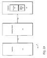
- FIG. 1Ais a schematic illustration of a SONET/SDH communication system in accordance with one embodiment.
- FIG. 1Bis a schematic illustration of a suitable system in accordance with one embodiment.
- FIG. 2Ais a schematic illustration of write operations into a memory at a receiver.
- FIG. 2Bis a schematic illustration of a memory at a receiver in accordance with one embodiment.
- FIG. 3is a flowchart illustrating operations in one embodiment of a method for writing data frames into a memory.
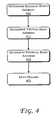
- FIG. 4is a flowchart illustrating operations in one embodiment of a method for reading data frames from a memory.
- FIG. 5is a schematic illustration of an eight-byte wide memory with N words in accordance with one embodiment.
- FIG. 6is a schematic illustration of one embodiment of a memory architecture in which M bytes of SDRAM store 64 STS-3c members.
- Described hereinare exemplary systems and methods for differential delay compensation in a communication system.
- numerous specific detailsare set forth in order to provide a thorough understanding of various embodiments. However, it will be understood by those skilled in the art that the various embodiments may be practiced without the specific details. In other instances, well-known methods, procedures, components, and circuits have not been described in detail so as not to obscure the particular embodiments.
- the methods described hereinmay be embodied as logic instructions on a computer-readable medium. When executed on a processor, the logic instructions cause a processor to be programmed as a special-purpose machine that implements the described methods.
- the processorwhen configured by the logic instructions to execute the methods described herein, constitutes structure for performing the described methods.
- FIG. 1Ais a schematic illustration of a SONET/SDH communication switching system in accordance with one embodiment.
- SONET/SDH switching system 100includes a transmitter 110 connected through a communication pathway 115 to a switching network 120 .
- Switching network 120is connected through a communication pathway 125 to a destination 130 .
- Transmitter 110transmits data as a series of payloads/frames to the destination 130 through the switching network 120 .
- Packetsmay pass through a variety of hardware and/or software components, such as servers, routers, switches, etc. in transmission across switching network 120 .
- the componentmay store the frame briefly before transmitting the frame to the next component.
- the framesproceed through the network until they arrive at the destination 130 .
- the destination 130may contain one or more processors 135 and/or one or more memory modules 140 .
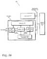
- FIG. 1Bis a schematic illustration of a suitable system in accordance with one embodiment.
- the system 101may include a line card 111 , a line card 121 , a switch fabric 141 , and a backplane interface 131 .
- Line card 111may be implemented as a SONET/SDH add-drop multiplexer, a Fibre Channel compatible line input, an Ethernet line input, a SONET/SDH line input, or the like.
- Line card 121may be implemented as a transceiver capable of transmitting and receiving frames and/or packets to and from a network that is compatible with SONET/SDH as well as other protocols such as OTN, TFI-5, and Ethernet, although other standards may be used.
- SONET/SDH and OTNare described for example in: ITU-T Recommendation G.709 Interfaces for the optical transport network (OTN) (2001); ANSI T1.105, Synchronous Optical Network (SONET) Basic Description Including Multiplex Structures, Rates, and Formats; Bellcore Generic Requirements, GR-253-CORE, Synchronous Optical Network (SONET) Transport Systems: Common Generic Criteria (A Module of TSGR, FR-440), Issue 1, December 1994; ITU Recommendation G.872, Architecture of Optical Transport Networks, 1999; ITU Recommendation G.825, “Control of Jitter and Wander within Digital Networks Based on SDH” March, 1993; ITU Recommendation G.957, “Optical Interfaces for Equipment and Systems Relating to SDH”, July, 1995; ITU Recommendation G.958, Digital Line Systems based on SDH for use on Optical Fibre Cables, November, 1994; and/or
- Switching network 120may be any network such as the Internet, an intranet, a local area network (LAN), storage area network (SAN), a wide area network (WAN).
- line card 121may include physical layer processor 122 , framer 124 , network processor 126 , and host-control plane controller 128 .
- Physical layer processor 122may receive optical or electrical signals from the network and prepare the signals for processing by downstream elements such as framer 124 . For example, for frames and/or packets received from the network, physical layer processor 122 may convert an optical signal to electrical format and/or remove jitter from signals from the network. For frames and/or packets to be transmitted to the network, physical layer processor 122 may remove jitter from signals provided by upstream devices such as framer 124 and prepare signals for transmission to the network, which may be optical or electrical format.
- Framer 124may utilize techniques described herein to process frames and/or packets received from a network.
- Framer 124may transfer overhead from frames and/or packets to a higher layer level processor such as a network processor 126 .
- a network processor 126may communicate using an interface compatible for example with SPI-4 (described for example in the Optical Internetworking Forum (OIF Document) OIF-SPI4-02.1 and ITU-T G.707 2000, T1.105-2001 (draft), T1.105.02-1995, and ITU-T recommendations G.7042 and G.707), although interfaces compatible with other standards may be used.
- SPI-4described for example in the Optical Internetworking Forum (OIF Document) OIF-SPI4-02.1 and ITU-T G.707 2000, T1.105-2001 (draft), T1.105.02-1995, and ITU-T recommendations G.7042 and G.707
- Network processor 126may perform layer 2 or layer 3 (as well as other higher layer level) processing on frames and/or packets provided by and to framer 124 in conformance with applicable link, network, transport and application protocols. Network processor 126 also may perform traffic management at the IP layer.
- Host-control plane controller 128may configure operation of framer 124 and network processor 126 .
- host-control plane controller 128may program/provision framer 124 to control the content of frames.
- Host-control plane controller 128may be implemented as separate from network processor 126 and communicate with the framer 124 and network processor 126 using an interface that complies with Peripheral Component Interconnect (PCI) Local Bus Specification, Revision 2.2, Dec. 18, 1998 available from the PCI Special Interest Group, Portland, Oreg., U.S.A. (as well as revisions thereof) or PCI-X Specification Rev. 1.0a, Jul.
- PCIPeripheral Component Interconnect
- Host-control plane controller 128could be implemented as part of network processor 126 , although other implementations may be used.
- one or more of physical layer processor 122 , framer 124 , or network processor 126may be coupled to volatile and/or nonvolatile memory module 127 .
- memory module 127may include one or more of the following: read-only memory (ROM), programmable ROM (PROM), erasable PROM (EPROM), electrically EPROM (EEPROM), a disk drive, a floppy disk, a compact disk ROM (CD-ROM), a digital video disk (DVD), flash memory, a magneto-optical disk, or other types of nonvolatile machine-readable media suitable for storing electronic instructions and/or data.
- components of line card 121may be implemented among the same integrated circuit. In another embodiment, components of line card 121 may be implemented among several integrated circuits that communicate using, for example, a bus or conductive leads of a printed circuit board.
- Backplane interfaces 131may be implemented as a single or multi-pin interface and may be used by line cards to interface with system fabric 141 .
- backplane interfaces 131may be compatible with TFI-5 or CSIX (described in CSIX-L1: Common Switch Interface Specification-L1 (2000)), although other standards may be used.
- Switch fabric 141may transfer IP packets or Ethernet packets (as well as other information) between line cards based on relevant address and header information.
- Switch fabric 141can be implemented as a packet switch fabric or a TDM cross connect.
- Switch fabric 141can be any device (or devices) that interconnect numerous dataplanes of subsystems (i.e., linecards) together.
- SONET/SDHdefines optical carrier levels and electrically equivalent synchronous transport signals (STSs) for the fiber-optic based hierarchy.
- STSssynchronous transport signals
- any type of serviceranging from voice to high speed data and video, can be accepted by various types of service adapters.
- a service adaptermaps the signal into the payload envelope of the STS-1 or virtual tributary. All inputs received are converted to a base format of a synchronous signal, referred to as STS-1, which transmits at 51.84 Mbps (or higher).
- STS-1a synchronous signal
- SONET networkstransmit data in frames, which include a transport overhead and a synchronous payload envelope (SPE).
- An SPEincludes an STS path overhead section and a payload section, which holds the data being transported over the SONET network. Once the payload is multiplexed into the SPE and transmitted, the payload is not examined at intermediate nodes.
- SONET/SDH architecturesupports virtual concatenation.
- virtual concatenationa large payload may be divided into a group of smaller payloads, which may be transmitted contemporaneously across different communication channels.
- Each SPE within a concatenated groupcontains an identifier, called a Multi-Frame Identifier, or MFI.
- MFIforms part of the SONET/SDH path overhead information in the SPE and indicates the SPE's sequence and position within the group.
- Virtual concatenationdoes not require intermediate node support.
- a receiver at the destinationtemporarily stores frames in a memory so that the payload data can be properly realigned.
- Applying an address calculation method that allows continuous data storage from members (i. e., time slots) in virtually concatenated groupspermits the efficient use of the memory, thereby increasing the differential delay range which may be compensated for a given memory size.
- a 1-byte wide on-chip memoryis used as an example. The scheme can be extended for wider memory or for external memory modules. On-chip memory or external RAM modules can be used as a memory.
- FIG. 2Ais a schematic illustration of a memory at a receiver
- FIG. 3is a flowchart illustrating operations in one embodiment of a method for writing data frames into a memory such as the buffer illustrated in FIG. 2A
- data framesare received at a destination node in a communication network.
- the payload data from the received data framesare stored in a memory.
- the physical write address at which a received frame is written in memoryis recorded in a suitable memory, for example a flip-flop or other memory device.
- the physical write addresscorresponds to a physical location in the memory.
- a virtual write addressis recorded in a suitable memory, for example a flip-flop or other memory device.
- the virtual write addressincludes the MFI value associated with the received data frame and the byte number for the last received byte.
- the payload data frames received at the receivermay be written into the memory continuously.
- the physical write addressis incremented continuously as frames are received.
- FIG. 2Aillustrates an embodiment in which a 2.5 KB (2560 bytes) memory is used to store STS-3c payloads, which include 2349 bytes per frame.
- the J1 byte for a given frame iis stored at address 130
- the J1 byte for frame i+1 and frame i+2are stored at address 2479 and 2268 , respectively. Writing data to the memory in a continuous fashion makes efficient use of the memory.
- FIG. 2Bis a schematic illustration of a memory at a receiver
- FIG. 4is a flowchart illustrating operations in one embodiment of a method for reading data frames from a memory such as the buffer illustrated in FIG. 2B .
- a minimum write address for a groupis determined from the virtual write addresses of all members belong to this group.
- the minimum write addressmay be determined by comparing the virtual write addresses of all members in the same group, and selecting the minimum write address.
- the minimum write addressmay be expressed using a multiframe indicator and a byte number.
- a virtual read addressis determined using the minimum write address.
- the virtual read addressis determined by subtracting a threshold value equal to the write to read delay in memory from the minimum write address.
- a physical read addressis determined using the virtual read address.
- the virtual read addressis the same for the whole group, due to the address conversion, each member may have a different physical read address. From the virtual read address, the actual byte number and MFI value can be identified easily for any follow up processing.
- the addressing schemeis illustrated schematically in FIG. 2B .
- a group of three members 240 - 244are shown.
- the J1 byte for member 240is at byte 130
- the J1 byte for member 242is at byte 2103
- the J1 byte for member 2is at byte 1027 .
- the current physical write addresses for each of members 240 , 242 , 244is at byte 2105 , which is indicated by hash marks in FIG. 2B . While in this example the physical write address for members 240 , 242 , 244 is the same, the physical write address may differ for members in the same group, e.g., due to different SONET pointer movements from different members.
- WA Phy(0)2105
- WA Phy(1)2105
- WA Phy(2)2105
- the byte at the current write addressis byte number 1975 in frame i, so it is denoted (i, 1975 ).
- the byte at current write addressis the second byte in frame i, so it is denoted as (i, 2 ).
- the byte at the current write addressis byte number 1078 in frame i, so it is denoted as (i, 1078 ).
- member 242has the minimum virtual write address.
- the threshold between the group read address and the minimum write address of the groupis 2.
- FIG. 5is a schematic illustration of an eight-byte wide memory 500 with N words in accordance with an embodiment.
- Received data framesmay be written continuously into the memory.
- any byte of the memorymay store a J1 byte of a received data frame.
- the address translation described above for one-byte wide memorycan be applied to an eight-byte wide memory.
- the memorymay be treated as a circular memory. Thus, when a write operation reaches the final byte of word N ⁇ 1, the write operation can continue with the first byte of word zero.
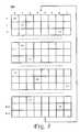
- FIG. 6is a schematic illustration of one embodiment of a memory architecture in which M bytes of SDRAM store 64 STS-3c members (e.g., for an OC-192 device).
- an M-byte block of SDRAM 610is divided into four banks identified by bank 0 ( 612 ), bank 1 ( 614 ), bank 2 ( 616 ), and bank 3 ( 618 ).
- Each of the four banks of SDRAM 610stores data from sixteen members.
- bank 0 ( 612 )stores data from the set of members ( 0 , 4 , 8 . . . 60 )
- bank 1 ( 614 )stores data from the set of members ( 1 , 5 , 9 . . .
- bank 2( 616 ) stores data from the set of members ( 2 , 6 , 10 , . . . 62 ), and bank 4 ( 618 ) stores data from the set of members ( 3 , 7 , 11 , . . . 63 ). Separating members into different banks in the SDRAM 610 improves the access efficiency when reading from and writing to SDRAM 610 .
- each bank 612 , 614 , 616 , 618may be divided into chunks of 1024 bytes, illustrated in table 630 . This allocates 64 bytes of memory to each of the sixteen members assigned to the bank, as illustrated in table 640 . In turn, each 64 byte memory allocation is divided into eight words of memory, each of which is 8 bits in width, as illustrated in table 650 .
- the memorymay be treated as a circular memory. Thus, when a write operation reaches the final byte of word M/512-1, the write operation can continue with the first byte of word zero.
Landscapes
- Engineering & Computer Science (AREA)
- Computer Networks & Wireless Communication (AREA)
- Signal Processing (AREA)
- Theoretical Computer Science (AREA)
- Computer Hardware Design (AREA)
- Physics & Mathematics (AREA)
- General Engineering & Computer Science (AREA)
- General Physics & Mathematics (AREA)
- Time-Division Multiplex Systems (AREA)
Abstract
Description
RAPhy(i)=WAPhy(i)−(WAVir(i)−RAVir)
where RAPhy (i) is the physical read address for member i, WAPhy (i) is the physical write address for member i, WAVir (i) is the virtual write address for member i, and RAVir is the virtual read address for the whole group.
WAPhy(0)=2105
WAPhy(1)=2105
WAPhy(2)=2105
WAVir(0)=(i,1975)
WAVir(1)=(i,2)
WAVir(2)=(i,1078)
RAVir=(i,0)
RAPhy(0)=130
RAPhy(1)=2103
RAPhy(2)=1027
Claims (12)
Priority Applications (2)
| Application Number | Priority Date | Filing Date | Title |
|---|---|---|---|
| US13/942,339US9110794B2 (en) | 2005-03-30 | 2013-07-15 | Differential delay compensation |
| US14/825,976US9430378B2 (en) | 2005-03-30 | 2015-08-13 | Differential delay compensation |
Applications Claiming Priority (3)
| Application Number | Priority Date | Filing Date | Title |
|---|---|---|---|
| US11/093,907US8018926B2 (en) | 2005-03-30 | 2005-03-30 | Differential delay compensation |
| US13/229,455US8488631B2 (en) | 2005-03-30 | 2011-09-09 | Differential delay compensation |
| US13/942,339US9110794B2 (en) | 2005-03-30 | 2013-07-15 | Differential delay compensation |
Related Parent Applications (1)
| Application Number | Title | Priority Date | Filing Date |
|---|---|---|---|
| US13/229,455ContinuationUS8488631B2 (en) | 2005-03-30 | 2011-09-09 | Differential delay compensation |
Related Child Applications (1)
| Application Number | Title | Priority Date | Filing Date |
|---|---|---|---|
| US14/825,976ContinuationUS9430378B2 (en) | 2005-03-30 | 2015-08-13 | Differential delay compensation |
Publications (2)
| Publication Number | Publication Date |
|---|---|
| US20130305010A1 US20130305010A1 (en) | 2013-11-14 |
| US9110794B2true US9110794B2 (en) | 2015-08-18 |
Family
ID=37070360
Family Applications (4)
| Application Number | Title | Priority Date | Filing Date |
|---|---|---|---|
| US11/093,907Active2028-05-17US8018926B2 (en) | 2005-03-30 | 2005-03-30 | Differential delay compensation |
| US13/229,455Expired - LifetimeUS8488631B2 (en) | 2005-03-30 | 2011-09-09 | Differential delay compensation |
| US13/942,339Expired - LifetimeUS9110794B2 (en) | 2005-03-30 | 2013-07-15 | Differential delay compensation |
| US14/825,976Expired - LifetimeUS9430378B2 (en) | 2005-03-30 | 2015-08-13 | Differential delay compensation |
Family Applications Before (2)
| Application Number | Title | Priority Date | Filing Date |
|---|---|---|---|
| US11/093,907Active2028-05-17US8018926B2 (en) | 2005-03-30 | 2005-03-30 | Differential delay compensation |
| US13/229,455Expired - LifetimeUS8488631B2 (en) | 2005-03-30 | 2011-09-09 | Differential delay compensation |
Family Applications After (1)
| Application Number | Title | Priority Date | Filing Date |
|---|---|---|---|
| US14/825,976Expired - LifetimeUS9430378B2 (en) | 2005-03-30 | 2015-08-13 | Differential delay compensation |
Country Status (1)
| Country | Link |
|---|---|
| US (4) | US8018926B2 (en) |
Cited By (1)
| Publication number | Priority date | Publication date | Assignee | Title |
|---|---|---|---|---|
| US9430378B2 (en) | 2005-03-30 | 2016-08-30 | Micron Technology, Inc. | Differential delay compensation |
Families Citing this family (7)
| Publication number | Priority date | Publication date | Assignee | Title |
|---|---|---|---|---|
| US8582607B2 (en)* | 2006-01-19 | 2013-11-12 | Ciena Corporation | Geographically-diverse redundant servers over optical connections with managed path differential delay |
| CN101814953B (en)* | 2010-03-01 | 2014-03-19 | 中兴通讯股份有限公司 | Method and system for realizing automatic protection switching of transmission equipment |
| US9467389B2 (en) | 2014-04-28 | 2016-10-11 | International Business Machines Corporation | Handling large frames in a virtualized fibre channel over ethernet (FCoE) data forwarder |
| CN108476181B (en)* | 2016-04-14 | 2020-08-25 | 华为技术有限公司 | Differential signal compensation method and device |
| CN107302513B (en)* | 2017-06-04 | 2019-12-31 | 西安征途网络科技有限公司 | Physical layer frame structure of broadband wireless transmission system suitable for TDD SC-FDE |
| FR3106422B1 (en)* | 2020-01-20 | 2021-12-10 | Continental Automotive | Motor vehicle data frame communication gateway |
| US12301467B2 (en) | 2022-10-18 | 2025-05-13 | Cisco Technology, Inc. | Differential path routing of multiple sub-flows split from larger bandwidth traffic flow |
Citations (23)
| Publication number | Priority date | Publication date | Assignee | Title |
|---|---|---|---|---|
| US4357681A (en) | 1980-05-07 | 1982-11-02 | Burroughs Corporation | Line turn circuit for data link |
| US4392207A (en) | 1980-09-09 | 1983-07-05 | Burroughs Corporation | Card reader-data link processor |
| US5119290A (en) | 1987-10-02 | 1992-06-02 | Sun Microsystems, Inc. | Alias address support |
| US5179686A (en) | 1990-08-16 | 1993-01-12 | Ncr Corporation | Method for automatically detecting the size of a memory by performing a memory warp operation |
| US5905725A (en) | 1996-12-16 | 1999-05-18 | Juniper Networks | High speed switching device |
| US6055285A (en) | 1997-11-17 | 2000-04-25 | Qlogic Corporation | Synchronization circuit for transferring pointer between two asynchronous circuits |
| US6279095B1 (en) | 1998-11-09 | 2001-08-21 | Compaq Computer Corporation | Method and apparatus for omnibus wiring of virtual mapping table entries |
| US20020083292A1 (en) | 2000-11-22 | 2002-06-27 | Seiko Epson Corporation | Method of using memory, two dimensional data access memory and operation processing apparatus |
| US20030095563A1 (en)* | 2001-08-30 | 2003-05-22 | Pmc-Sierra, Inc. | Differential delay compensation |
| US6675327B1 (en) | 1998-12-14 | 2004-01-06 | Agere Systems Inc. | Communications system including lower rate parallel electronics with skew compensation and associated methods |
| US6697368B2 (en) | 2000-11-17 | 2004-02-24 | Foundry Networks, Inc. | High-performance network switch |
| US20040037182A1 (en) | 2002-08-21 | 2004-02-26 | Nec Corporation | Phase adjusting apparatus, phase adjusting method for use therein, and program for phase adjusting method |
| US6775302B1 (en) | 1998-12-14 | 2004-08-10 | Agere Systems Inc. | Communications system with symmetrical interfaces and associated methods |
| US6782466B1 (en) | 1999-11-24 | 2004-08-24 | Koninklijke Philips Electronics N.V. | Arrangement and method for accessing data in a virtual memory arrangement |
| US20050094669A1 (en)* | 2003-10-30 | 2005-05-05 | Sanjay Bhardwaj | Virtual concatenation receiver processing with memory addressing scheme to avoid delays at address scatter points |
| US6917630B1 (en) | 1998-10-06 | 2005-07-12 | Nortel Networks Limited | Concatenation of containers in synchronous digital hierarchy network |
| US6944168B2 (en) | 2001-05-04 | 2005-09-13 | Slt Logic Llc | System and method for providing transformation of multi-protocol packets in a data stream |
| US20060256710A1 (en) | 2005-05-13 | 2006-11-16 | Intel Corporation | Techniques for group alarm indication signal generation and clearing |
| US7296139B1 (en)* | 2004-01-30 | 2007-11-13 | Nvidia Corporation | In-memory table structure for virtual address translation system with translation units of variable range size |
| US7315540B2 (en) | 2002-07-31 | 2008-01-01 | Texas Instruments Incorporated | Random access memory based space time switch architecture |
| US7508830B1 (en) | 2004-08-27 | 2009-03-24 | Intel Corporation | Method and apparatus differential delay compensation processing of virtually concatenated data |
| US7606269B1 (en) | 2004-07-27 | 2009-10-20 | Intel Corporation | Method and apparatus for detecting and managing loss of alignment in a virtually concatenated group |
| US8018926B2 (en) | 2005-03-30 | 2011-09-13 | Jing Ling | Differential delay compensation |
- 2005
- 2005-03-30USUS11/093,907patent/US8018926B2/enactiveActive
- 2011
- 2011-09-09USUS13/229,455patent/US8488631B2/ennot_activeExpired - Lifetime
- 2013
- 2013-07-15USUS13/942,339patent/US9110794B2/ennot_activeExpired - Lifetime
- 2015
- 2015-08-13USUS14/825,976patent/US9430378B2/ennot_activeExpired - Lifetime
Patent Citations (25)
| Publication number | Priority date | Publication date | Assignee | Title |
|---|---|---|---|---|
| US4357681A (en) | 1980-05-07 | 1982-11-02 | Burroughs Corporation | Line turn circuit for data link |
| US4392207A (en) | 1980-09-09 | 1983-07-05 | Burroughs Corporation | Card reader-data link processor |
| US5119290A (en) | 1987-10-02 | 1992-06-02 | Sun Microsystems, Inc. | Alias address support |
| US5179686A (en) | 1990-08-16 | 1993-01-12 | Ncr Corporation | Method for automatically detecting the size of a memory by performing a memory warp operation |
| US5905725A (en) | 1996-12-16 | 1999-05-18 | Juniper Networks | High speed switching device |
| US6055285A (en) | 1997-11-17 | 2000-04-25 | Qlogic Corporation | Synchronization circuit for transferring pointer between two asynchronous circuits |
| US6917630B1 (en) | 1998-10-06 | 2005-07-12 | Nortel Networks Limited | Concatenation of containers in synchronous digital hierarchy network |
| US6279095B1 (en) | 1998-11-09 | 2001-08-21 | Compaq Computer Corporation | Method and apparatus for omnibus wiring of virtual mapping table entries |
| US6775302B1 (en) | 1998-12-14 | 2004-08-10 | Agere Systems Inc. | Communications system with symmetrical interfaces and associated methods |
| US6675327B1 (en) | 1998-12-14 | 2004-01-06 | Agere Systems Inc. | Communications system including lower rate parallel electronics with skew compensation and associated methods |
| US6782466B1 (en) | 1999-11-24 | 2004-08-24 | Koninklijke Philips Electronics N.V. | Arrangement and method for accessing data in a virtual memory arrangement |
| US6697368B2 (en) | 2000-11-17 | 2004-02-24 | Foundry Networks, Inc. | High-performance network switch |
| US20020083292A1 (en) | 2000-11-22 | 2002-06-27 | Seiko Epson Corporation | Method of using memory, two dimensional data access memory and operation processing apparatus |
| US6944168B2 (en) | 2001-05-04 | 2005-09-13 | Slt Logic Llc | System and method for providing transformation of multi-protocol packets in a data stream |
| US20030095563A1 (en)* | 2001-08-30 | 2003-05-22 | Pmc-Sierra, Inc. | Differential delay compensation |
| US7315540B2 (en) | 2002-07-31 | 2008-01-01 | Texas Instruments Incorporated | Random access memory based space time switch architecture |
| US20040037182A1 (en) | 2002-08-21 | 2004-02-26 | Nec Corporation | Phase adjusting apparatus, phase adjusting method for use therein, and program for phase adjusting method |
| US20050094669A1 (en)* | 2003-10-30 | 2005-05-05 | Sanjay Bhardwaj | Virtual concatenation receiver processing with memory addressing scheme to avoid delays at address scatter points |
| US7296139B1 (en)* | 2004-01-30 | 2007-11-13 | Nvidia Corporation | In-memory table structure for virtual address translation system with translation units of variable range size |
| US7606269B1 (en) | 2004-07-27 | 2009-10-20 | Intel Corporation | Method and apparatus for detecting and managing loss of alignment in a virtually concatenated group |
| US7508830B1 (en) | 2004-08-27 | 2009-03-24 | Intel Corporation | Method and apparatus differential delay compensation processing of virtually concatenated data |
| US8018926B2 (en) | 2005-03-30 | 2011-09-13 | Jing Ling | Differential delay compensation |
| US20110317721A1 (en) | 2005-03-30 | 2011-12-29 | Jing Ling | Differential delay compensation |
| US8488631B2 (en) | 2005-03-30 | 2013-07-16 | Micron Technology, Inc. | Differential delay compensation |
| US20060256710A1 (en) | 2005-05-13 | 2006-11-16 | Intel Corporation | Techniques for group alarm indication signal generation and clearing |
Non-Patent Citations (16)
| Title |
|---|
| "", ITU-T Telecommunication Sector of ITU, G. 707/Y.1322, (Oct. 2000), 184 pgs. |
| "", ITU-T Telecommunication Sector of ITU, G. 709/Y.1331, (Feb. 2001), 79 pgs. |
| "Architecture of Optical Transport Networks", Series G: Transmission Systems and Media, Digital Systems and Networks; ITU-T, G.872, (Feb. 1999), 37 pgs. |
| "Common Switch Interface Specification-L1", CSIX-L1, Version 1.0, (Aug. 2000), 68 pgs. |
| "Control of Jitter and Wander within Digital Networks Based on SDH", Digital Networks, ITU, G.825, (Mar. 1993), 8 pgs. |
| "Digital Line Systems Based on SDH for Use on Optical Fibre Cables", Digital Sections and Digital Line Systems, ITU, G.958, (Nov. 1994), 25 pgs. |
| "Internetworking Technology Overview", Ethernet/IEEE 802.3, Chapter 7, (Jun. 1999), 24 pgs. |
| "Link Capacity Adjustment Scheme (LCAS) for Virtual Concatenated Signals", ITU-T, G.7042/Y.1305, (Mar. 2006), 38 pgs. |
| "Optical Interfaces for Equipment and Systems Relating to SDH", Series G: Transmission Systems and Media, Digital Systems and Networks, ITU, G.957, (Jun. 1999), 38 pgs. |
| "PCI Local Bus Specification", Revision 2.2, (Dec. 1998), 322 pgs. |
| "PCI-X Addendum to the PCI Local Bus Specification", Revision 1.0a, (Jul. 2000), 240 pgs. |
| "Synchronous Optical Network (SONET) Basic Description Including Multiplex Structure, Rates, and Formats", ANSI T1.105, (May 2001), 107 pgs. |
| "Synchronous Optical Network (SONET) Transport Systems: Common Generic Criteria-TSGR", GR-253-CORE; FR-440, Bellcore, (Dec. 1995), 786 pgs. |
| "System Packet Interface Level 4 (SPI-4) Phase 2 Revision 1: OC-192 System Interface for Physical and Link Layer Devices", OIF-SPI-4-02.1, (Oct. 2003), 66 pgs. |
| "TDM Fabric to Framer Interface Implementation Agreement", OIF-TFI-5-01.0, (Sep. 2003), 71 pgs. |
| "Transmission and Multiplexing (TM); Optical Interfaces for Equipments and Systems Relating to the Synchronous Digital Hierarchy (SDH)", ETS 300 232 Amendment A1, ITU, G.957, (Mar. 1996), 6 pgs. |
Cited By (1)
| Publication number | Priority date | Publication date | Assignee | Title |
|---|---|---|---|---|
| US9430378B2 (en) | 2005-03-30 | 2016-08-30 | Micron Technology, Inc. | Differential delay compensation |
Also Published As
| Publication number | Publication date |
|---|---|
| US20130305010A1 (en) | 2013-11-14 |
| US20110317721A1 (en) | 2011-12-29 |
| US8488631B2 (en) | 2013-07-16 |
| US8018926B2 (en) | 2011-09-13 |
| US9430378B2 (en) | 2016-08-30 |
| US20060221944A1 (en) | 2006-10-05 |
| US20150350114A1 (en) | 2015-12-03 |
Similar Documents
| Publication | Publication Date | Title |
|---|---|---|
| US9430378B2 (en) | Differential delay compensation | |
| EP1634414B1 (en) | Multi-rate, multi-protocol, multi-port line interface for a multiservice switching platform | |
| JP3864258B2 (en) | Data transmission method and apparatus | |
| US8107362B2 (en) | Multi-ring resilient packet ring add/drop device | |
| EP1794910B1 (en) | Overhead processing and generation techniques | |
| US7197031B2 (en) | Cross-connection of high bandwidth signal traffic across independent parallel shelves | |
| JP3828013B2 (en) | Transmission system | |
| US7583599B1 (en) | Transporting stream client signals via packet interface using GFP mapping | |
| US20040105453A1 (en) | Capacity re-use in data communication networks | |
| US7298744B1 (en) | Method and apparatus for centralized processing of contiguously and virtually concatenated payloads | |
| US7542484B2 (en) | Managing payload specific latencies in a cross-connect system | |
| US7508830B1 (en) | Method and apparatus differential delay compensation processing of virtually concatenated data | |
| US7554975B2 (en) | Protocol agnostic switching | |
| US7606269B1 (en) | Method and apparatus for detecting and managing loss of alignment in a virtually concatenated group | |
| US7050391B1 (en) | Method and apparatus for efficient link redundancy | |
| US7656891B1 (en) | Method and apparatus enabling concurrent processing of contiguously and virtually concatenated payloads | |
| US7564777B2 (en) | Techniques for group alarm indication signal generation and clearing | |
| US7313151B2 (en) | Extendible asynchronous and synchronous interface bus for broadband access | |
| WO2002080420A1 (en) | Capacity re-use in data communication networks |
Legal Events
| Date | Code | Title | Description |
|---|---|---|---|
| FEPP | Fee payment procedure | Free format text:PAYOR NUMBER ASSIGNED (ORIGINAL EVENT CODE: ASPN); ENTITY STATUS OF PATENT OWNER: LARGE ENTITY | |
| STCF | Information on status: patent grant | Free format text:PATENTED CASE | |
| AS | Assignment | Owner name:U.S. BANK NATIONAL ASSOCIATION, AS COLLATERAL AGENT, CALIFORNIA Free format text:SECURITY INTEREST;ASSIGNOR:MICRON TECHNOLOGY, INC.;REEL/FRAME:038669/0001 Effective date:20160426 Owner name:U.S. BANK NATIONAL ASSOCIATION, AS COLLATERAL AGEN Free format text:SECURITY INTEREST;ASSIGNOR:MICRON TECHNOLOGY, INC.;REEL/FRAME:038669/0001 Effective date:20160426 | |
| AS | Assignment | Owner name:MORGAN STANLEY SENIOR FUNDING, INC., AS COLLATERAL AGENT, MARYLAND Free format text:PATENT SECURITY AGREEMENT;ASSIGNOR:MICRON TECHNOLOGY, INC.;REEL/FRAME:038954/0001 Effective date:20160426 Owner name:MORGAN STANLEY SENIOR FUNDING, INC., AS COLLATERAL Free format text:PATENT SECURITY AGREEMENT;ASSIGNOR:MICRON TECHNOLOGY, INC.;REEL/FRAME:038954/0001 Effective date:20160426 | |
| AS | Assignment | Owner name:U.S. BANK NATIONAL ASSOCIATION, AS COLLATERAL AGENT, CALIFORNIA Free format text:CORRECTIVE ASSIGNMENT TO CORRECT THE REPLACE ERRONEOUSLY FILED PATENT #7358718 WITH THE CORRECT PATENT #7358178 PREVIOUSLY RECORDED ON REEL 038669 FRAME 0001. ASSIGNOR(S) HEREBY CONFIRMS THE SECURITY INTEREST;ASSIGNOR:MICRON TECHNOLOGY, INC.;REEL/FRAME:043079/0001 Effective date:20160426 Owner name:U.S. BANK NATIONAL ASSOCIATION, AS COLLATERAL AGEN Free format text:CORRECTIVE ASSIGNMENT TO CORRECT THE REPLACE ERRONEOUSLY FILED PATENT #7358718 WITH THE CORRECT PATENT #7358178 PREVIOUSLY RECORDED ON REEL 038669 FRAME 0001. ASSIGNOR(S) HEREBY CONFIRMS THE SECURITY INTEREST;ASSIGNOR:MICRON TECHNOLOGY, INC.;REEL/FRAME:043079/0001 Effective date:20160426 | |
| AS | Assignment | Owner name:JPMORGAN CHASE BANK, N.A., AS COLLATERAL AGENT, ILLINOIS Free format text:SECURITY INTEREST;ASSIGNORS:MICRON TECHNOLOGY, INC.;MICRON SEMICONDUCTOR PRODUCTS, INC.;REEL/FRAME:047540/0001 Effective date:20180703 Owner name:JPMORGAN CHASE BANK, N.A., AS COLLATERAL AGENT, IL Free format text:SECURITY INTEREST;ASSIGNORS:MICRON TECHNOLOGY, INC.;MICRON SEMICONDUCTOR PRODUCTS, INC.;REEL/FRAME:047540/0001 Effective date:20180703 | |
| AS | Assignment | Owner name:MICRON TECHNOLOGY, INC., IDAHO Free format text:RELEASE BY SECURED PARTY;ASSIGNOR:U.S. BANK NATIONAL ASSOCIATION, AS COLLATERAL AGENT;REEL/FRAME:047243/0001 Effective date:20180629 | |
| MAFP | Maintenance fee payment | Free format text:PAYMENT OF MAINTENANCE FEE, 4TH YEAR, LARGE ENTITY (ORIGINAL EVENT CODE: M1551); ENTITY STATUS OF PATENT OWNER: LARGE ENTITY Year of fee payment:4 | |
| AS | Assignment | Owner name:MICRON TECHNOLOGY, INC., IDAHO Free format text:RELEASE BY SECURED PARTY;ASSIGNOR:MORGAN STANLEY SENIOR FUNDING, INC., AS COLLATERAL AGENT;REEL/FRAME:050937/0001 Effective date:20190731 | |
| AS | Assignment | Owner name:MICRON TECHNOLOGY, INC., IDAHO Free format text:RELEASE BY SECURED PARTY;ASSIGNOR:JPMORGAN CHASE BANK, N.A., AS COLLATERAL AGENT;REEL/FRAME:051028/0001 Effective date:20190731 Owner name:MICRON SEMICONDUCTOR PRODUCTS, INC., IDAHO Free format text:RELEASE BY SECURED PARTY;ASSIGNOR:JPMORGAN CHASE BANK, N.A., AS COLLATERAL AGENT;REEL/FRAME:051028/0001 Effective date:20190731 | |
| MAFP | Maintenance fee payment | Free format text:PAYMENT OF MAINTENANCE FEE, 8TH YEAR, LARGE ENTITY (ORIGINAL EVENT CODE: M1552); ENTITY STATUS OF PATENT OWNER: LARGE ENTITY Year of fee payment:8 |