US9110015B2 - Method and system for delta double sampling - Google Patents
Method and system for delta double samplingDownload PDFInfo
- Publication number
- US9110015B2 US9110015B2US14/569,289US201414569289AUS9110015B2US 9110015 B2US9110015 B2US 9110015B2US 201414569289 AUS201414569289 AUS 201414569289AUS 9110015 B2US9110015 B2US 9110015B2
- Authority
- US
- United States
- Prior art keywords
- transistor
- comparator
- signal
- chemically
- sample
- Prior art date
- Legal status (The legal status is an assumption and is not a legal conclusion. Google has not performed a legal analysis and makes no representation as to the accuracy of the status listed.)
- Expired - Fee Related
Links
- 238000005070samplingMethods0.000titleclaimsdescription66
- 238000000034methodMethods0.000titleclaimsdescription23
- 239000000523sampleSubstances0.000claimsdescription62
- 238000006243chemical reactionMethods0.000claimsdescription39
- 239000003990capacitorSubstances0.000claimsdescription27
- 239000013074reference sampleSubstances0.000claimsdescription17
- 230000004044responseEffects0.000claimsdescription13
- 238000012512characterization methodMethods0.000claimsdescription12
- 230000008569processEffects0.000claimsdescription8
- 239000000126substanceSubstances0.000claimsdescription7
- 238000001914filtrationMethods0.000claimsdescription3
- 230000006870functionEffects0.000description17
- 150000002500ionsChemical class0.000description17
- 238000003491arrayMethods0.000description14
- 238000002161passivationMethods0.000description13
- 239000012491analyteSubstances0.000description11
- 230000002596correlated effectEffects0.000description9
- 238000001514detection methodMethods0.000description7
- 238000004519manufacturing processMethods0.000description7
- 238000007667floatingMethods0.000description6
- 150000007523nucleic acidsChemical class0.000description6
- 102000039446nucleic acidsHuman genes0.000description6
- 108020004707nucleic acidsProteins0.000description6
- 229910021420polycrystalline siliconInorganic materials0.000description6
- 229920005591polysiliconPolymers0.000description6
- 238000012545processingMethods0.000description6
- 230000008901benefitEffects0.000description5
- 229910052751metalInorganic materials0.000description5
- 239000002184metalSubstances0.000description5
- 230000009467reductionEffects0.000description5
- 239000000758substrateSubstances0.000description5
- 101100102849Saccharomyces cerevisiae (strain ATCC 204508 / S288c) VTH1 geneProteins0.000description4
- 238000010586diagramMethods0.000description4
- 238000005516engineering processMethods0.000description4
- -1hydrogen ionsChemical class0.000description4
- 239000000463materialSubstances0.000description4
- 238000005259measurementMethods0.000description4
- 229910044991metal oxideInorganic materials0.000description4
- 150000004706metal oxidesChemical class0.000description4
- 239000002773nucleotideSubstances0.000description4
- 125000003729nucleotide groupChemical group0.000description4
- 239000004065semiconductorSubstances0.000description4
- 230000035945sensitivityEffects0.000description4
- XUIMIQQOPSSXEZ-UHFFFAOYSA-NSiliconChemical compound[Si]XUIMIQQOPSSXEZ-UHFFFAOYSA-N0.000description3
- 239000004020conductorSubstances0.000description3
- 238000013461designMethods0.000description3
- 230000000694effectsEffects0.000description3
- 229910052739hydrogenInorganic materials0.000description3
- 239000001257hydrogenSubstances0.000description3
- 238000012544monitoring processMethods0.000description3
- 238000012163sequencing techniqueMethods0.000description3
- 229910052710siliconInorganic materials0.000description3
- 239000010703siliconSubstances0.000description3
- 230000009897systematic effectEffects0.000description3
- 238000001712DNA sequencingMethods0.000description2
- YZCKVEUIGOORGS-UHFFFAOYSA-NHydrogen atomChemical compound[H]YZCKVEUIGOORGS-UHFFFAOYSA-N0.000description2
- XEEYBQQBJWHFJM-UHFFFAOYSA-NIronChemical compound[Fe]XEEYBQQBJWHFJM-UHFFFAOYSA-N0.000description2
- 238000013459approachMethods0.000description2
- 230000008859changeEffects0.000description2
- 239000002800charge carrierSubstances0.000description2
- 150000001875compoundsChemical class0.000description2
- 238000012937correctionMethods0.000description2
- 230000000875corresponding effectEffects0.000description2
- 238000011161developmentMethods0.000description2
- 230000005669field effectEffects0.000description2
- GPRLSGONYQIRFK-UHFFFAOYSA-NhydronChemical compound[H+]GPRLSGONYQIRFK-UHFFFAOYSA-N0.000description2
- 238000010348incorporationMethods0.000description2
- 238000011160researchMethods0.000description2
- 230000003068static effectEffects0.000description2
- 230000001629suppressionEffects0.000description2
- WKBOTKDWSSQWDR-UHFFFAOYSA-NBromine atomChemical compound[Br]WKBOTKDWSSQWDR-UHFFFAOYSA-N0.000description1
- OYPRJOBELJOOCE-UHFFFAOYSA-NCalciumChemical compound[Ca]OYPRJOBELJOOCE-UHFFFAOYSA-N0.000description1
- OKTJSMMVPCPJKN-UHFFFAOYSA-NCarbonChemical compound[C]OKTJSMMVPCPJKN-UHFFFAOYSA-N0.000description1
- 229910001218Gallium arsenideInorganic materials0.000description1
- DGAQECJNVWCQMB-PUAWFVPOSA-MIlexoside XXIXChemical compoundC[C@@H]1CC[C@@]2(CC[C@@]3(C(=CC[C@H]4[C@]3(CC[C@@H]5[C@@]4(CC[C@@H](C5(C)C)OS(=O)(=O)[O-])C)C)[C@@H]2[C@]1(C)O)C)C(=O)O[C@H]6[C@@H]([C@H]([C@@H]([C@H](O6)CO)O)O)O.[Na+]DGAQECJNVWCQMB-PUAWFVPOSA-M0.000description1
- 229910002651NO3Inorganic materials0.000description1
- NHNBFGGVMKEFGY-UHFFFAOYSA-NNitrateChemical compound[O-][N+]([O-])=ONHNBFGGVMKEFGY-UHFFFAOYSA-N0.000description1
- NPYPAHLBTDXSSS-UHFFFAOYSA-NPotassium ionChemical compound[K+]NPYPAHLBTDXSSS-UHFFFAOYSA-N0.000description1
- 229910052581Si3N4Inorganic materials0.000description1
- BQCADISMDOOEFD-UHFFFAOYSA-NSilverChemical compound[Ag]BQCADISMDOOEFD-UHFFFAOYSA-N0.000description1
- 229910052770UraniumInorganic materials0.000description1
- 108010067973ValinomycinProteins0.000description1
- 229910052782aluminiumInorganic materials0.000description1
- XAGFODPZIPBFFR-UHFFFAOYSA-NaluminiumChemical compound[Al]XAGFODPZIPBFFR-UHFFFAOYSA-N0.000description1
- 230000002238attenuated effectEffects0.000description1
- 239000011324beadSubstances0.000description1
- 230000031018biological processes and functionsEffects0.000description1
- GDTBXPJZTBHREO-UHFFFAOYSA-NbromineSubstancesBrBrGDTBXPJZTBHREO-UHFFFAOYSA-N0.000description1
- 229910052794bromiumInorganic materials0.000description1
- 239000011575calciumSubstances0.000description1
- 229910052791calciumInorganic materials0.000description1
- 239000002041carbon nanotubeSubstances0.000description1
- 229910021393carbon nanotubeInorganic materials0.000description1
- 125000003636chemical groupChemical group0.000description1
- 238000001311chemical methods and processMethods0.000description1
- 230000000295complement effectEffects0.000description1
- FCFNRCROJUBPLU-UHFFFAOYSA-Ncompound M126Natural productsCC(C)C1NC(=O)C(C)OC(=O)C(C(C)C)NC(=O)C(C(C)C)OC(=O)C(C(C)C)NC(=O)C(C)OC(=O)C(C(C)C)NC(=O)C(C(C)C)OC(=O)C(C(C)C)NC(=O)C(C)OC(=O)C(C(C)C)NC(=O)C(C(C)C)OC1=OFCFNRCROJUBPLU-UHFFFAOYSA-N0.000description1
- 238000004590computer programMethods0.000description1
- 230000008878couplingEffects0.000description1
- 238000010168coupling processMethods0.000description1
- 238000005859coupling reactionMethods0.000description1
- 230000000779depleting effectEffects0.000description1
- 238000009792diffusion processMethods0.000description1
- 238000010494dissociation reactionMethods0.000description1
- 230000005593dissociationsEffects0.000description1
- 238000000407epitaxyMethods0.000description1
- 230000001747exhibiting effectEffects0.000description1
- 238000003384imaging methodMethods0.000description1
- PNDPGZBMCMUPRI-UHFFFAOYSA-NiodineChemical compoundIIPNDPGZBMCMUPRI-UHFFFAOYSA-N0.000description1
- 229910052742ironInorganic materials0.000description1
- 239000007788liquidSubstances0.000description1
- 239000012528membraneSubstances0.000description1
- 238000012986modificationMethods0.000description1
- 230000004048modificationEffects0.000description1
- 230000001537neural effectEffects0.000description1
- 230000007935neutral effectEffects0.000description1
- 150000004767nitridesChemical class0.000description1
- 230000003287optical effectEffects0.000description1
- BPUBBGLMJRNUCC-UHFFFAOYSA-Noxygen(2-);tantalum(5+)Chemical class[O-2].[O-2].[O-2].[O-2].[O-2].[Ta+5].[Ta+5]BPUBBGLMJRNUCC-UHFFFAOYSA-N0.000description1
- 229920000915polyvinyl chloridePolymers0.000description1
- 239000004800polyvinyl chlorideSubstances0.000description1
- 229910001414potassium ionInorganic materials0.000description1
- 238000013139quantizationMethods0.000description1
- HQVNEWCFYHHQES-UHFFFAOYSA-Nsilicon nitrideChemical compoundN12[Si]34N5[Si]62N3[Si]51N64HQVNEWCFYHHQES-UHFFFAOYSA-N0.000description1
- 229910052709silverInorganic materials0.000description1
- 239000004332silverSubstances0.000description1
- 229910052708sodiumInorganic materials0.000description1
- 239000011734sodiumSubstances0.000description1
- 239000007787solidSubstances0.000description1
- 229910001936tantalum oxideInorganic materials0.000description1
- 230000002123temporal effectEffects0.000description1
- 238000012546transferMethods0.000description1
- 230000009466transformationEffects0.000description1
- 235000011178triphosphateNutrition0.000description1
- 239000001226triphosphateSubstances0.000description1
- UNXRWKVEANCORM-UHFFFAOYSA-Ntriphosphoric acidChemical compoundOP(O)(=O)OP(O)(=O)OP(O)(O)=OUNXRWKVEANCORM-UHFFFAOYSA-N0.000description1
- FCFNRCROJUBPLU-DNDCDFAISA-NvalinomycinChemical compoundCC(C)[C@@H]1NC(=O)[C@H](C)OC(=O)[C@@H](C(C)C)NC(=O)[C@@H](C(C)C)OC(=O)[C@H](C(C)C)NC(=O)[C@H](C)OC(=O)[C@@H](C(C)C)NC(=O)[C@@H](C(C)C)OC(=O)[C@H](C(C)C)NC(=O)[C@H](C)OC(=O)[C@@H](C(C)C)NC(=O)[C@@H](C(C)C)OC1=OFCFNRCROJUBPLU-DNDCDFAISA-N0.000description1
- 230000000007visual effectEffects0.000description1
Images


Classifications
- G—PHYSICS
- G01—MEASURING; TESTING
- G01N—INVESTIGATING OR ANALYSING MATERIALS BY DETERMINING THEIR CHEMICAL OR PHYSICAL PROPERTIES
- G01N27/00—Investigating or analysing materials by the use of electric, electrochemical, or magnetic means
- G01N27/26—Investigating or analysing materials by the use of electric, electrochemical, or magnetic means by investigating electrochemical variables; by using electrolysis or electrophoresis
- G01N27/403—Cells and electrode assemblies
- G01N27/414—Ion-sensitive or chemical field-effect transistors, i.e. ISFETS or CHEMFETS
- G01N27/4148—Integrated circuits therefor, e.g. fabricated by CMOS processing
- H—ELECTRICITY
- H03—ELECTRONIC CIRCUITRY
- H03K—PULSE TECHNIQUE
- H03K5/00—Manipulating of pulses not covered by one of the other main groups of this subclass
- H03K5/003—Changing the DC level
- Y—GENERAL TAGGING OF NEW TECHNOLOGICAL DEVELOPMENTS; GENERAL TAGGING OF CROSS-SECTIONAL TECHNOLOGIES SPANNING OVER SEVERAL SECTIONS OF THE IPC; TECHNICAL SUBJECTS COVERED BY FORMER USPC CROSS-REFERENCE ART COLLECTIONS [XRACs] AND DIGESTS
- Y10—TECHNICAL SUBJECTS COVERED BY FORMER USPC
- Y10S—TECHNICAL SUBJECTS COVERED BY FORMER USPC CROSS-REFERENCE ART COLLECTIONS [XRACs] AND DIGESTS
- Y10S436/00—Chemistry: analytical and immunological testing
- Y10S436/806—Electrical property or magnetic property
- Y—GENERAL TAGGING OF NEW TECHNOLOGICAL DEVELOPMENTS; GENERAL TAGGING OF CROSS-SECTIONAL TECHNOLOGIES SPANNING OVER SEVERAL SECTIONS OF THE IPC; TECHNICAL SUBJECTS COVERED BY FORMER USPC CROSS-REFERENCE ART COLLECTIONS [XRACs] AND DIGESTS
- Y10—TECHNICAL SUBJECTS COVERED BY FORMER USPC
- Y10S—TECHNICAL SUBJECTS COVERED BY FORMER USPC CROSS-REFERENCE ART COLLECTIONS [XRACs] AND DIGESTS
- Y10S436/00—Chemistry: analytical and immunological testing
- Y10S436/807—Apparatus included in process claim, e.g. physical support structures
- Y—GENERAL TAGGING OF NEW TECHNOLOGICAL DEVELOPMENTS; GENERAL TAGGING OF CROSS-SECTIONAL TECHNOLOGIES SPANNING OVER SEVERAL SECTIONS OF THE IPC; TECHNICAL SUBJECTS COVERED BY FORMER USPC CROSS-REFERENCE ART COLLECTIONS [XRACs] AND DIGESTS
- Y10—TECHNICAL SUBJECTS COVERED BY FORMER USPC
- Y10T—TECHNICAL SUBJECTS COVERED BY FORMER US CLASSIFICATION
- Y10T436/00—Chemistry: analytical and immunological testing
- Y10T436/11—Automated chemical analysis
Definitions
- the presently disclosed embodimentsdeal with pixel arrays, and more particularly, to mismatch suppression and offset cancellation of components within the pixel arrays and readout circuits.
- ISFETion-sensitive field effect transistor
- pHFETpHFET
- ISFETsconventionally have been explored, primarily in the academic and research community, to facilitate measurement of the hydrogen ion concentration of a solution (commonly denoted as “pH”).
- An ISFETis referred to, more generally, as a chemically-sensitive sensor herein.
- an ISFETis an impedance transformation device that operates in a manner similar to that of a MOSFET (Metal Oxide Semiconductor Field Effect Transistor), and is particularly configured to selectively measure ion activity in a solution (e.g., hydrogen ions in the solution are the “analytes”).
- MOSFETMetal Oxide Semiconductor Field Effect Transistor
- a detailed theory of operation of an ISFETis given in “Thirty years of ISFETOLOGY: what happened in the past 30 years and what may happen in the next 30 years,” P. Bergveld, Sens. Actuators, 88 (2003), pp. 1-20 (“Bergveld”), which publication is hereby incorporated herein by reference in its entirety.
- biCMOSi.e., bipolar and CMOS
- CMOScomplementary metal-oxide-semiconductor
- CMOScomplementary metal-oxide-semiconductor
- CMOScomplementary metal-oxide-semiconductor
- other technologiesmay be employed wherein a sensing element can be made with a three-terminal devices in which a sensed ion leads to the development of a signal that controls one of the three terminals; such technologies may also include, for example, GaAs and carbon nanotube technologies.
- a P-type ISFET fabricationis based on a P-type or N-type silicon substrate, in which an n-type well forming a transistor “body” is formed.
- a highly doped N-type (N+) region Bmay also be formed within the n-type well to provide a conductive body (or “bulk”) connection to the n-type well.
- An oxide layermay be disposed above the source, drain and body connection regions, through which openings are made to provide electrical connections (via electrical conductors) to these regions.
- a polysilicon gatemay be formed above the oxide layer at a location above a region of the N-type well, between the source and the drain. Because it is disposed between the polysilicon gate and the transistor body (i.e., the N-type well), the oxide layer often is referred to as the “gate oxide.”
- an N-type ISFET fabricationis based on a P+ wafer substrate with a P ⁇ epitaxy region of typically several microns thick, in which a P-type well creating a transistor “body” is formed.
- the P-type wellis shared amongst all devices in the array and the P+ substrate serves as the bulk contact such that no other contacts are required at the pixel array.
- Highly doped N-type (N+) regions S and D, constituting a source and a drain of the ISFET,are formed within the P-type well.
- An oxide layermay be disposed above the source, drain and body connection regions, through which openings are made to provide electrical connections (via electrical conductors) to these regions.
- a polysilicon gatemay be formed above the oxide layer at a location above a region of the N-type well, between the source and the drain. Because it is disposed between the polysilicon gate and the transistor body (i.e., the p-type well), the oxide layer often is referred to as the “gate oxide.”
- an ISFETLike a MOSFET, the operation of an ISFET is based on the modulation of charge concentration (and thus channel conductance) caused by a MOS (Metal-Oxide-Semiconductor) capacitance.
- This capacitanceis constituted by a polysilicon gate, a gate oxide and a region of the well (e.g., N-type well) between the source and the drain.
- a negative voltageis applied across the gate and source regions, a channel is created at the interface of the region and the gate oxide by depleting this area of electrons.
- the channelwould be a P-channel (and vice-versa).
- the P-channelIn the case of an N-well, the P-channel would extend between the source and the drain, and electric current is conducted through the P-channel when the gate-source potential is negative enough to attract holes from the source into the channel.
- the gate-source potential at which the channel begins to conduct currentis referred to as the transistor's threshold voltage VTH (the transistor conducts when VGS has an absolute value greater than the threshold voltage VTH).
- the sourceis so named because it is the source of the charge carriers (holes for a P-channel) that flow through the channel; similarly, the drain is where the charge carriers leave the channel.
- an ISFETmay be fabricated with a floating gate structure, formed by coupling a polysilicon gate to multiple metal layers disposed within one or more additional oxide layers disposed above the gate oxide.
- the floating gate structureis so named because it is electrically isolated from other conductors associated with the ISFET; namely, it is sandwiched between the gate oxide and a passivation layer that is disposed over a metal layer (e.g., top metal layer) of the floating gage.
- the ISFET passivation layerconstitutes an ion-sensitive membrane that gives rise to the ion-sensitivity of the device.
- analytessuch as ions in an analyte solution (i.e., a solution containing analytes (including ions) of interest or being tested for the presence of analytes of interest), in contact with the passivation layer, particularly in a sensitive area that may lie above the floating gate structure, alters the electrical characteristics of the ISFET so as to modulate a current flowing through the channel between the source and the drain of the ISFET.
- the passivation layermay comprise any one of a variety of different materials to facilitate sensitivity to particular ions; for example, passivation layers comprising silicon nitride or silicon oxynitride, as well as metal oxides such as silicon, aluminum or tantalum oxides, generally provide sensitivity to hydrogen ion concentration (pH) in an analyte solution, whereas passivation layers comprising polyvinyl chloride containing valinomycin provide sensitivity to potassium ion concentration in an analyte solution.
- passivation layersmay comprise various materials (e.g., metal oxides, metal nitrides, metal oxynitrides).
- the surface of a given material employed for the passivation layer of the ISFETmay include chemical groups that may donate protons to or accept protons from the analyte solution, leaving at any given time negatively charged, positively charged, and neutral sites on the surface of the passivation layer at the interface with the analyte solution.
- an electricstatic potential differencearises at the solid/liquid interface of the passivation layer and the analyte solution as a function of the ion concentration in the sensitive area due to a chemical reaction (e.g., usually involving the dissociation of oxide surface groups by the ions in the analyte solution in proximity to the sensitive area).
- This surface potentialin turn affects the threshold voltage of the ISFET; thus, it is the threshold voltage of the ISFET that varies with changes in ion concentration in the analyte solution in proximity to the sensitive area.
- the source voltage VSprovides a signal that is directly related to the ion concentration in the analyte solution in proximity to the sensitive area of the ISFET.
- chemFETschemically-sensitive FETs
- ISFETschemically-sensitive FETs
- chemFETsmay be used for monitoring reactions—including, for example, nucleic acid (e.g., DNA) sequencing reactions, based on monitoring analytes present, generated or used during a reaction.
- arrays including large arrays of chemFETsmay be employed to detect and measure static and/or dynamic amounts or concentrations of a variety of analytes (e.g., hydrogen ions, other ions, non-ionic molecules or compounds, etc.) in a variety of chemical and/or biological processes (e.g., biological or chemical reactions, cell or tissue cultures or monitoring, neural activity, nucleic acid sequencing, etc.) in which valuable information may be obtained based on such analyte measurements.
- Such chemFET arraysmay be employed in methods that detect analytes and/or methods that monitor biological or chemical processes via changes in charge at the chemFET surface.
- ChemFET (or ISFET) arraysinvolves detection of analytes in solution and/or detection of change in charge bound to the chemFET surface (e.g. ISFET passivation layer).
- Rothbergdescribes using a chemFET array (in particular ISFETs) for sequencing a nucleic acid involving incorporating known nucleotides into a plurality of identical nucleic acids in a reaction chamber in contact with or capacitively coupled to chemFET, wherein the nucleic acids are bound to a single bead in the reaction chamber, and detecting a signal at the chemFET, wherein detection of the signal indicates release of one or more hydrogen ions resulting from incorporation of the known nucleotide triphosphate into the synthesized nucleic acid.
- chemFET arrayin particular ISFETs
- a problem that exists within many of these circuits and arraysrelates to tolerances in the circuit fabrication process.
- the same types of circuitsmay have somewhat different characteristics from one another because of inherent variances in the circuit components and their relative structures that occur from fabrication tolerances. These differences in circuits that are intended to be identical circuits is often referred to as a mismatch.
- An example of offset and mismatchmay be an amplifier mismatch that occurs in circuits due to threshold mismatch between the devices of the input differential pair that are intended to be identical.
- Arrays having numerous amplifiers that are intended to be identical, but are not,are typical of circuits that can exhibit mismatch.
- Active pixel sensorsare an example of devices where this mismatch and offset may be critical.
- Active pixel sensorsare image sensing arrays having a number of pixels, and each pixel is associated with an amplifier to output the light sensed by that pixel.
- a common approach to correcting for amplifier mismatch within active pixel sensorsis correlated double sampling. In correlated double sampling, one sample is taken of a reset pixel value and another sample taken of the pixel with the signal from sensed light. A difference is taken between the two samples.
- the difference in samplesshould represent the actual signal free of offsets including a reduction in thermal noise if the samples are time correlated. In order to acquire the two samples, a reset value is required. Correlated double sampling can be effective in removing various types of offsets and transistor mismatch problems.
- sensing arraysthat have sensing elements that are continually being read over a time period may not enable reset circuits to be used within those sensing elements. Without this reset value to be sampled, correlated double sampling is not a useable technique because of the absence of a reset value or reference value that is correlated to the sensing devices. Therefore, there is a need in the prior art for providing double sampling circuits that cannot employ correlated double sampling techniques.
- transistor mismatch in CMOS circuitscan impose severe limitations for sensor arrays. This may be especially true for sensors with small output levels.
- the total deviation that inherently results during the fabrication processescreates non-uniformity in the transistors within the array of sensors resulting in signal offsets and non-uniformity within the signal created by these transistors. Therefore, it is desirable to eliminate or reduce such non-uniformity and offsets, especially before the A/D conversion. From the foregoing discussion, there remains a need within the art for a circuit that can eliminate offsets and mismatches within circuits, even those without reset capabilities.
- FIG. 1is an exemplary circuit that may exhibit transistor mismatch.
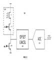
- FIG. 2is an exemplary block diagram incorporating components according to an embodiment of the present invention.
- FIGS. 3A and 3Billustrate examples of matched transistor pairs used for sampling according to an embodiment of the present invention.
- FIG. 4is an example of a sampling circuit using a matched transistor pair for sampling according to an embodiment of the present invention.
- FIG. 5is an exemplary timing diagram for operation the sampling circuit of FIG. 4 according to an embodiment of the present invention.
- FIG. 6illustrates another example of a sampling circuit using a matched transistor pair for sampling according to an embodiment of the present invention.
- a method to attenuate circuit component offsets and mismatchesmay be provided.
- a pixel outputmay be precharged to a first bias level.
- the pixelmay include a chemically-sensitive sensor and a select transistor that are a matched pair of transistors.
- a a reference signal sample from the select transistor in the pixelmay be sampled. Offset and mismatch signal artifacts from the reference sample may be canceled to leave an offset and mismatch correction signal at a circuit node.
- a selected input signal from the chemically-sensitive sensor in the pixelis sampled.
- the sampled input signalmay be adjusted according to the offset and mismatch correction signal at the circuit node.
- the adjusted sampled input signalmay be converted from an analog signal to a digital signal.
- the systemincludes a pixel having a chemically-sensitive sensor for providing an input signal in response to a chemical reaction, and a select transistor for providing a reference sample.
- the systemmay also included a sampling circuit, a comparator circuit and a latch.
- the sampling circuitmay be configured to take the reference sample from the select transistor and an input signal sample from the chemically-sensitive sensor through the select transistor.
- the comparator circuitmay output a first comparison result of the reference sample to a reference voltage and to perform analog-to-digital conversion by outputting a second comparison result that includes a signal indicating a value of the input signal sample in comparison to a digital threshold reference signal.
- the latchmay provide a control signal to the sampling circuit in response to the first comparison result and output a digital signal value in response to the second comparison result.
- Another embodimentprovides for a system including a single transistor chemically-sensitive pixel and a characterization transistor.
- the single transistor chemically-sensitive pixelmay provide an input signal in response to a chemical reaction.
- the characterization transistormay provide a reference sample, wherein the characterization transistor is outside the pixel.
- FIG. 1is an example of a circuit exhibiting transistor and amplifier mismatch.
- the circuit 100may have offsets and mismatches in pixel 110 , transistors 105 , 125 , 127 , and buffer 130 may combine to create signal non-uniformity.
- the pixel 110may be a two transistor 112 and 114 pixel that does not have a reset function.
- One of the transistors 112may be a chemically-sensitive sensor that detects a small signal resulting from a chemical reaction that generates a signal as a result.
- An analog to digital converter (ADC)(not shown) may be connected to the output of buffer 130 to convert the analog output signal to a digital signal.
- ADCanalog to digital converter
- the ADCin order to accurately resolve the analog output signal to a digital signal, will require additional bits allocated over a wide dynamic range—the more non-uniform the output signal from buffer 130 , the more bits will be required.
- the amplitude of the desired signal contained on the signal output from the output of buffer 130is small compared to the entire output signal, the greater the effect signal non-uniformity has on the overall signal, which results in an inefficient allocation of bits. The offsets and mismatches, therefore, impose higher bit-depth requirements.
- the required dynamic range of an off-chip ADCmay be, for example, approximately 250 mV. This dynamic range may provide for large signal sizes and a high degree of resolution.
- a small signal that is contained on a signal that is large in amplitude due to a non-uniform nature of the signalmay have requirements to reach a quantization noise level of 10 uV, and require a 12-14 bit resolution for an ADC in order to be accurately resolved.
- FIG. 2illustrates an exemplary block diagram incorporating components according to an embodiment of the present invention.
- the system 200may include a pixel 210 , a bias transistor 230 , an offset cancel block 240 , and an analog-to-digital converter 250 .
- the pixel 210may include a matched pair of transistors: a chemically-sensitive sensor 211 and a row select transistor 215 , where matched transistors means that the transistors 211 and 215 are both similar size, shape and type. To qualify as matched pair, not all properties of the devices need be identical. For example, both transistors may have the same width and share the same diffusion region but have nominally different gate lengths. Since the devices are minimally spaced apart, their gate oxide regions will be well matched.
- the threshold of the devicesto be well matched in comparison to devices that are further separated.
- Devices with different gate lengthswill produce a measured difference in output levels but all matched pairs will be behave in the same systematic way and preserve uniformity.
- One differencemay be that the chemically-sensitive sensor 211 may differ from row select transistor 215 by having a chemically-sensitive well coupled to a floating gate that provides an input signal. Other differences may exist as long as the differences are systematic and remain consistent between the matched pairs.
- transistors formed close togetherhave less mismatch.
- the benefit of using matched transistors 211 and 215 in the same pixelis that, because the row select transistor is adjacent to the chemically-sensitive sensor, it will have less transistor mismatch.
- a reference levelmay be taken from the row select transistor in the same pixel as the chemically-sensitive sensor as an approximate matching reference for the sensor transistor.
- all of the components in the pixel 210 and bias transistor 230may have some form of offsets and mismatches that may contribute to output signal non-uniformity.
- the combined offset and mismatch in pixel 210 and bias transistor 230may be sampled into the offset cancel block 240 and removed before analog-to-digital conversion by the ADC 250 .
- dynamic range requirements of the ADC 250may drop to, for example, an 8-bit level since only the actual signal level is converted.
- the transistor mismatchis removed or reduced and the sensor response is made uniform.
- the biasing transistor 230which may be a FET, may function to bias the pixel 210 through a bias voltage vb at the gate of biasing transistor 230 .
- the ADC 250provides a digital output for the signal from pixel 210 .
- Offset Cancel 240may be a column level circuit that provides double sampling capabilities to analyze pixel 210 .
- the offset functions of the Offset Cancel 240may eliminate the combined offsets and mismatches within pixel 210 , biasing transistor 230 and any other components in the signal path.
- the Offset Cancel 240may receive a first sample of the entire signal path absent the sensed signal on chemically-sensitive sensor 211 .
- the first samplemay include the combined offsets and mismatches of all the components, for example, chemically-sensitive sensor 211 and transistor 215 of pixel 210 and biasing transistor 230 , in the entire signal path.
- a second sample of the signal pathmay be taken with the sensed signal value from the chemically-sensitive sensor 211 included in the sampled value.
- the second sample of the entire signal pathmay include the combined offsets and mismatches of all the components, for example, chemically-sensitive sensor 211 and transistor 215 of pixel 210 and biasing transistor 230 , in the entire signal path as well as the sensed signal value of chemically-sensitive sensor 211 .
- Offset Cancel 240may provide a difference function that subtracts the first sample from the second sample including the sensed signal value from the chemically-sensitive sensor 21 , which leaves the sensed signal value to be provided to the ADC 250 .
- the Offset Cancel 240may take the two samples, may employ a double sampling technique on the two samples, and may remove offsets and mismatches of pixel 210 , and biasing transistor 230 using the two samples before analog to digital conversion by ADC 250 .
- the dynamic range requirement of ADC 250may be reduced since only the actual sensed, signal-level of chemically-sensitive sensor is converted.
- the bit lengthdrops to an 8-bit level since only the actual signal level is converted. As a result, circuit component mismatch is removed/reduced and sensor response is made uniform.
- FIGS. 3A and 3Billustrate an example of delta double sampling using the matched pair of transistors according to an embodiment of the present invention.
- the pixel 310may be biased by a current source I (e.g., a transistor such as transistor 230 of FIG. 2 ).
- the pixel 310may include a chemically-sensitive sensor 313 , and a row select transistor 315 , both of which may be a FET.
- the matched pairincludes chemically-sensitive sensor 313 and row select transistor 315 . These devices are considered a matched pair due to their close proximity and the properties in the example of FIG. 2 .
- the pixel 310may be one of a plurality of pixels that are used within an array (not shown) that is arranged in rows and columns.
- Select transistor 315may be controlled by a row select signal rs that is used to select the pixel 310 .
- a signal samplemay be taken of the device in two different states. A sample may be taken of the pixel 310 in a first state without an input signal (known or unknown, or in a reset mode), so any offsets or mismatches of the device may be characterized, and another sample may taken of the pixel 310 in a second state of the device that typically includes the input signal.
- the difference between the two samplesis considered a representation of the input signal without the presence of the pixel 310 offsets (e.g., transistor fabrication differences such as voltage threshold differences).
- the chemically-sensitive sensor 313may be read out continuously while the reaction being monitored is occurring. Accordingly, there is no opportunity to take a sample without an input signal or a known input signal from the chemically-sensitive sensor 313 .
- the reaction being monitored and read out continuously as it occursmay be a hydrogen ion (H+) released during a DNA sequencing event that occurs when a nucleotide is incorporated into a strand of DNA by a polymerase. As each nucleotide incorporates, a hydrogen ion (H+) is released. Since the chemically-sensitive sensor 313 is being read continuously during the period of time the incorporation signal is being generated, the chemically-sensitive sensor 313 cannot be reset, which eliminates the possibility of using correlated double sampling to remove and attenuate offsets. Since the actual chemically-sensitive sensor 313 cannot be measured without its input signal, the actual chemically-sensitive sensor 313 is replaced by its nearest neighbor, the row select transistor 315 to establish the correlation.
- H+hydrogen ion
- the row select transistor 315may provide the closest approximation of the offset and mismatch characteristics of the chemically-sensitive sensor 313 since it is locally matched to the chemically-sensitive sensor 313 .
- the row select transistor 315may likely share common mismatches and offsets with the chemically-sensitive sensor 313 since the row select transistor 315 is fabricated with, and is in close proximity to the chemically-sensitive sensor 313 .
- the row select transistor 315can be biased by a voltage V1 such that it operates in the saturation region to establish a local threshold voltage correlation (VTH1). Essentially, the row select transistor 315 hides the input signal when it is forced into saturation.
- the voltage V1is also less than VREF, which may be the effective DC bias level of the sensor electrode as it appears at the gate of the sensor transistor 313 .
- An exemplary voltage for V1may be approximately 1.5V and an exemplary voltage for VREF may be approximately 2.5V.
- This local threshold voltage correlation (VTH1)may be used to perform (delta) double sampling.
- the first signal sample S1may be equal to V1 ⁇ (VTH1+ ⁇ V), where ⁇ V is the overdrive voltage for biasing the transistor at the given bias current level. This value may remain constant within a pixel but may vary between pixels and largely from column to column due to bias current mismatches in the column-level bias circuitry.
- the first sample S1may be output from the circuit 300 at output Sout.
- FIG. 3Billustrates the taking of the second signal sample S2.
- the row select transistor 315can be biased by a voltage V2 such that it operates in the triode region to establish a local threshold voltage correlation of the transistor 313 (VTH2).
- the voltage V2is greater than VREF, which may be an effective supply voltage.
- VREFmay be a constant bias voltage that does not change between the reference sample and the signal sample.
- This local threshold voltage correlation (VTH2)may be used to perform (delta) double sampling.
- the second signal sample S2may include the input signal VSig and VREF from the chemically-sensitive sensor 313 .
- the second signal sample S2may equal VREF+VSig ⁇ (VTH2+ ⁇ V).
- the second sample S2may also be output from the circuit 300 at output Sout.
- a differencing functionmay produce the result of S2 ⁇ S1 as approximately equal to VSig+(VREF ⁇ V1)+(VTH1 ⁇ VTH2), note that the constant voltages ⁇ V cancel.
- the voltage (VREF ⁇ V1)may be a constant voltage set to an ADC reference voltage, in which case, the ADC may effectively remove the (VREF ⁇ V1) term.
- the threshold voltages VTH1 and VTH2may be substantially equal or the difference may be a systematic constant resulting from the matched pair configuration. Therefore, the resulting residue from (VTH1 ⁇ VTH2) may be minimal and consistent across the array of pixels. Any constant residue in this difference term may be absorbed in the ADC reference. More specifically, this difference term is zero when the transistors are of equal size.
- the resulting residuemay simply be added together with the other constant terms that establish the ADC reference.
- additional signal offset artifactsmay be collected in the first sample and be attenuated during the differencing function of the delta double sampling operation. This allows for double sampling the entire signal chain before the ADC.
- Portions of the ADCmay also become part of the offset cancellation scheme as well. For example, if the ADC has an input stage that is subject to offsets, these offsets may be cancelled as part of the two samples without requiring two separate data conversions. Of course, the order of the sampling may differ.
- the voltages V1 and V2may be programmable, and may switch on between row selection of the respective pixel during readout and the cascode level.
- the double sampling algorithmcan also be applied after the ADC, whereby the ADC performs two data conversion cycles and the difference between the samples is performed in digital logic.
- the digital logicmay be implemented as hardware on-chip or by software or hardware off-chip. This may be considered digital delta double sampling. This has advantages where multiple ADCs convert columns of pixel readouts simultaneously and where the ADCs have inherent offsets. Further, double delta double sampling may be performed by applying the differencing functions both before the ADC and after the ADC.
- the first differencing functionmay establishe a largely uniform signal for input into the ADC, thereby reducing the required dynamic range of the ADC.
- the second differencing functionmay be placed after the ADC to cancel the offsets in the ADCs.
- the first and second differencing functionsproduce complete offset cancellation of all circuit components.
- MPDDSmatched-pair delta double sampling
- FIG. 4illustrates a system according to an embodiment of the present invention.
- the system 400may include four circuit blocks: a pixel 410 , column sample circuit 420 , a comparator 406 , and a column latch 430 .
- Biasing transistor 405may bias pixel 410 based on bias signal vb.
- Transistor 408may provide a precharge signal based on the control input sw. This transistor 408 can be of either type depending on whether the column is precharged to the supply voltage, the substrate voltage or some other reference voltage in between the supply and substrate voltages.
- the pixel 410may be a two transistor design with a row select transistor 414 connected to the source of a chemically-sensitive sensor 412 .
- the drain of the chemically-sensitive sensor 412may be coupled to a supply voltage Vdda. In practice, this can be a column line that is switched to the Vdda supply voltage.
- the source of the row select transistor 414may output from the pixel 410 and couple to column sample circuit 420 and the biasing transistor 405 .
- the column sample 420may provide a readout circuit for reading out pixels 410 .
- the column sample 420may include a double cascoded current source including transistors 421 , 423 , and 427 (which form a current source) and transistors 425 and 420 (which form switches to enable the current source), a sampling capacitor C 1 , a reset transistor 422 , and current steering transistor 424 .
- the input signals Vbp, Vbpc and Vbpccprovide respective bias signals to bias the current provided by the respective transistors 421 , 423 , and 427 .
- the comparator 406may provide a comparison function for an input received from the column sample circuit 420 and a reference voltage Vramp.
- the comparator 406may have inverting and non-inverting inputs, control inputs and an output, and may be a high gain amplifier with a low input-referred noise level.
- the bandwidth of the comparator 406may be controlled by internal or external control signals (not shown) from a control circuit to vary the bandwidth of the comparator, such that the comparator's bandwidth can be changed from one phase to another depending upon the function that is desired from the comparator 406 .
- the comparator 406may be connected to the column latch 430 .
- the column latch 430may be an SR-latch.
- the latch 430may be reset with ‘latch_rst’ and set with either ‘latch_set’ or the output of the comparator.
- the output of the latch circuit 430may feed back to the column sample 420 .
- the comparator 406 and column latch circuit 430may be used for offset cancellation during the first sample phase and then later used for the A/D conversion in the second phase. Therefore, the only additional circuitry needed for the MPDDS system 400 may be a sampling capacitor and a few transistors.
- the sampling capacitor C 1may be made smaller than the required KTC noise level by keeping the bandwidth of the comparator 406 larger than the bandwidth of the current source mirror fashioned by transistors 421 , 423 and 427 .
- the reduction in KTC noise achieved in the sampling capacitoris known to those skilled in the art.
- the KTC noise reductionis being used with delta double sampling to achieve offset cancellation with a small layout footprint.
- the offset cancellation circuitry and the ADCare largely integrated together as one unit, while still performing separate operations.
- FIG. 5illustrates the timing of operation of the MPDDS system 400 of FIG. 4 .
- the timing of the MPDDS system 400may categorized into five phases of operation as shown in FIG. 5 : a precharge phase, a row select (select_rst) phase; an offset cancel phase; select signal phase and convert phase.
- the pixel 410 column linemay be switched to a constant bias level such as analog ground.
- the col_latch 430may be reset by switching ‘latch_rst’ low.
- the sampling capacitor C 1 terminal at transistor 422may be switched to ground and held low throughout the subsequent row select phase.
- initial biasing conditionsare established. No rows are selected during this phase so the pixel column line, represented by vpix, is driven to the initial biasing conditions.
- the level of prechargemay be set to a level higher than ground in order to effectively turn off the unselected pixels.
- the ‘rs’ linemay be switched to a mid-level voltage (for example 1.5V) that causes the row select device 414 to enter saturation and charge the column line.
- the reference voltage on the chemically-sensitive sensor 412may be at a higher level than the ‘rs’ line during this phase (for example 2.5V). This ensures that the row select device 414 stays in saturation.
- the value of the column linemay be driven to the voltage of the gate of the row select device 414 less the threshold voltage and the gate to source overdrive voltage required for a given bias current.
- the row select device 414Because the gate of the row select device 414 is held at a lower voltage than the gate of the chemically-sensitive sensor 412 , the row select device 414 operates in the saturation region and does not behave like a switch. Since the output resistance of the drain of row select device 414 is very high, the signal and noise at the source of chemically-sensitive sensor 412 cannot modulate the source of row select device 414 . This blocks the signal and noise at the input of the pixel during the offset cancel phase. Therefore, instead of resetting the pixel 410 to obtain the correlation value, the signal from the data path is blocked by forcing row select device 414 into saturation. Details of the biasing conditions and equations were discussed above with respect to FIGS. 3A and 3B .
- both lines ‘A’ and ‘B’are turned off, and the latch 430 is reset again while the vramp line to the comparator 406 is increased to its maximum level, which may exceed the effectively output level of the bias and signal level at the chemically-sensitive sensor 412 .
- the offset cancel periodmay contain timing sequences which effectively emulate a negative feedback loop which servos the voltage of the capacitor C 1 to the value needed to match the reference voltage at the comparator set by the Vramp input. The goal is to charge the sampling capacitor C 1 to a value that causes the comparator 406 to fire for the given reference at the Vramp input to the comparator 406 .
- the vp nodeinitially starts at a voltage established during the precharge period such as ground.
- the vp voltagemay be initialized to a voltage lower than the vramp reference voltage including the magnitude of the total mismatch between all comparators 406 .
- the input (vramp) to the comparator 406is being swept by the vp input until the comparator 406 fires.
- the current sourceis turned off and the value that is required to fire the comparator 406 is locked into the capacitor C 1 .
- any new input levels presented on the vpix linei.e., column line
- the difference (delta) between the new value and the initial valuewill only be represented to the comparator 406 as the difference (delta) between the new value and the initial value. Therefore, the subtraction between the samples is inherent in the configuration.
- the bandwidth of the comparator 406 in this phasemay be controlled to be at a certain, first bandwidth to provide fast operation and KTC noise suppression.
- the ‘rs’ lineis switched to its highest potential, which pushes the row select device 414 into triode region.
- the signal level at the chemically-sensitive sensor 412is now presented on the column line attached to the sampling capacitor C 1 .
- the chemically-sensitive sensor 412 voltageis then coupled through the sampling capacitor C 1 and held while the vramp voltage falls.
- a gray code countmay be distributed to all the columns.
- the ramp linei.e. Vramp
- Vrampmay be set to a voltage which always exceeds the new vpix voltage.
- the vramp linemay decrease in voltage in synchronization with the gray code counter.
- the ramp value (Vramp)causes the comparator 406 to fire, the corresponding gray code gets latched into local registers corresponding to that column line. The latched gray code then represents the offset cancelled signal.
- the bandwidth of the comparator 406 in the later conversion phasemay be controlled to be at a second bandwidth to provide slower operation compared to the earlier offset cancellation phase. By operating slower, the comparator may provide filtering of thermal fluidic noise generated by the system.
- the offset cancel phasehas been described with a comparator 406 , latch 430 and a current source within column sample 420 to charge the sampling capacitor C 1 .
- a continuous-time feedbackand treat the comparator 406 as an operational amplifier.
- the output of the amplifieris switched onto the inverting input terminal of the amplifier.
- the high gain in the comparator 406forces the input terminals to become substantially equal.
- the offset of the comparator 406 and the offsets before the capacitor C 1are sampled and cancelled when the amplifier operates in the open loop configuration during the conversion phase.
- the continuous time negative feedback loopperforms the required offset cancellation.
- the method described using the column latch configurationcan make use of a smaller capacitor than the continuous time implementation because the thermal noise from sampling can be reduced with the proper allocation of bandwidths.
- the comparatormay have larger bandwidth than the current source charging circuit. In order to achieve this larger bandwidth, the output resistance of the charging circuit may be kept to a high level by using multiple cascode devices.
- FIG. 6illustrates an alternate embodiment of the system MPDDS according to an embodiment of the present invention.
- the system 600may include a pixel 610 , column sample circuit 620 , a comparator 606 , and a column latch 630 .
- Biasing transistor 605may bias pixel 610 based on bias signal vb.
- the pixel 610may be a two transistor design with a row select transistor 614 connected to the source of a chemically-sensitive sensor 612 .
- the drain of the chemically-sensitive sensor 612may be coupled to a supply voltage Vdda.
- the source of the row select transistor 614may output from the pixel 610 and couple to column sample circuit 620 and the biasing transistor 605 .
- the column sample 620may provide a readout circuit for reading out pixels 610 .
- the column sample 620may include transistors 621 , 623 , 624 and 629 (which form a mirrored current source), a sampling capacitor C 1 , a reset transistor 622 , and current steering transistor 624 .
- the comparator 606may provide a comparison function for an input received from the column sample circuit 620 and a reference voltage Vramp.
- the comparator 606may be a high gain amplifier with a low input-referred noise level.
- the comparator 606may be connected to the column latch 630 .
- the column latch 630may be an SR-latch.
- the latch 630may be reset with ‘Latch_reset’ and set with either ‘Latch_set’ or the output of the comparator.
- the output of the latch circuit 630may feedback to the column sample 620 .
- the system 600operates substantially the same as the system 400 described above.
- the system 600may also operate according to the timing diagram of FIG. 5 .
- a primary differenceis the configuration of the column sample circuit 620 is different from the column sample circuit 420 (formed from transistors 421 , 423 - 425 , 427 and 429 ).
- the mirrored current source formed from transistors 621 , 623 , 624 and 629 for charging the sampling capacitor C 1is different.
- the currentis redirected when the latch trips whereas the current is simply turned off in FIG. 6 .
- the column sample 420 configuration of FIG. 4has an advantage in that the current supplied to the circuit 400 during the cancellation period is constant.
- Constant current operationcan reduce disturbances on the power supplies (not shown) that might otherwise corrupt other circuits performing the same operation.
- Another difference of the column sample circuit 620may be the configuration of inverters 631 as compared to the inverters in column sample circuit 420 .
- the inverter 631 configurationmay provide additional delay as compared to the inverters in column sample circuit 420 .
- the double samplingmay be performed against current matching.
- an additional transistor(s) outside the pixelreferred to as characterization transistor
- the characterization pixelmay be made larger to the approximate size of the chemically-sensitive transistor (excluding floating gate structure) to reduce mismatch.
- Signal samples (current or voltage) taken of the additional characterization transistor(s)may be used to characterize offsets and mismatches of the single chemically-sensitive transistor pixel.
- the additional transistorsmay be sampled to provide a reference sample that characterizes the pixel, and the pixel may be sampled.
- the pixel currentmay be sampled, and the current switched to pass through the larger transistors outside the pixel, and the current through the large transistors may be sampled.
- the delta double samplemay be taken between the pixel current in one sample and the characterization transistor current in another sample. Note that the threshold mismatching may be minimal.
- Mismatch and offsetsare removed without the cost of increased temporal noise. It should be noted that while the pixel-to-pixel mismatch is reduced, all other offsets in the signal path are removed. Other benefits may be, for example, low frequency noise (flicker noise) may reduced due to rapid double sampling. In addition to being capable of removing the offset at the signal path level, the offset may also be removed at the pixel 310 level for each individual pixel. Specifically, the 1/f noise in the comparator is reduced using delta double sampling because the interval between samples of the comparator is reduced by several orders of magnitude.
- Various embodimentsmay be implemented using hardware elements, software elements, or a combination of both.
- hardware elementsmay include processors, microprocessors, circuits, circuit elements (e.g., transistors, resistors, capacitors, inductors, and so forth), integrated circuits, application specific integrated circuits (ASIC), programmable logic devices (PLD), digital signal processors (DSP), field programmable gate array (FPGA), logic gates, registers, semiconductor device, chips, microchips, chip sets, and so forth.
- Examples of softwaremay include software components, programs, applications, computer programs, application programs, system programs, machine programs, operating system software, middleware, firmware, software modules, routines, subroutines, functions, methods, procedures, software interfaces, application program interfaces (API), instruction sets, computing code, computer code, code segments, computer code segments, words, values, symbols, or any combination thereof. Determining whether an embodiment is implemented using hardware elements and/or software elements may vary in accordance with any number of factors, such as desired computational rate, power levels, heat tolerances, processing cycle budget, input data rates, output data rates, memory resources, data bus speeds and other design or performance constraints.
- Some embodimentsmay be implemented, for example, using a computer-readable medium or article which may store an instruction or a set of instructions that, if executed by a machine, may cause the machine to perform a method and/or operations in accordance with the embodiments.
- a machinemay include, for example, any suitable processing platform, computing platform, computing device, processing device, computing system, processing system, computer, processor, or the like, and may be implemented using any suitable combination of hardware and/or software.
- the computer-readable medium or articlemay include, for example, any suitable type of memory unit, memory device, memory article, memory medium, storage device, storage article, storage medium and/or storage unit, for example, memory, removable or non-removable media, erasable or non-erasable media, writeable or re-writeable media, digital or analog media, hard disk, floppy disk, Compact Disc Read Only Memory (CD-ROM), Compact Disc Recordable (CD-R), Compact Disc Rewriteable (CD-RW), optical disk, magnetic media, magneto-optical media, removable memory cards or disks, various types of Digital Versatile Disc (DVD), a tape, a cassette, or the like.
- any suitable type of memory unitfor example, any suitable type of memory unit, memory device, memory article, memory medium, storage device, storage article, storage medium and/or storage unit, for example, memory, removable or non-removable media, erasable or non-erasable media, writeable or re-writeable media, digital or analog media, hard disk
- the instructionsmay include any suitable type of code, such as source code, compiled code, interpreted code, executable code, static code, dynamic code, encrypted code, and the like, implemented using any suitable high-level, low-level, object-oriented, visual, compiled and/or interpreted programming language.
Landscapes
- Physics & Mathematics (AREA)
- Chemical & Material Sciences (AREA)
- Engineering & Computer Science (AREA)
- Microelectronics & Electronic Packaging (AREA)
- Health & Medical Sciences (AREA)
- Life Sciences & Earth Sciences (AREA)
- Nonlinear Science (AREA)
- Electrochemistry (AREA)
- Molecular Biology (AREA)
- Computer Hardware Design (AREA)
- Analytical Chemistry (AREA)
- Chemical Kinetics & Catalysis (AREA)
- Biochemistry (AREA)
- General Health & Medical Sciences (AREA)
- General Physics & Mathematics (AREA)
- Immunology (AREA)
- Pathology (AREA)
- Transforming Light Signals Into Electric Signals (AREA)
Abstract
Description
This application is a continuation of U.S. patent application Ser. No. 14/334,291 filed Jul. 17, 2014 which is a continuation of U.S. patent application Ser. No. 13/173,851 filed Jun. 30, 2011, now issued U.S. Pat. No. 8,796,036, which claims the benefit of U.S. Provisional Patent Application Ser. No. 61/386,403 filed on Sep. 24, 2010, the content of which is incorporated herein by reference in its entirety.
The presently disclosed embodiments deal with pixel arrays, and more particularly, to mismatch suppression and offset cancellation of components within the pixel arrays and readout circuits.
Electronic devices and components have found numerous applications in chemistry and biology (more generally, “life sciences”), especially for detection and measurement of various chemical and biological reactions and identification, detection and measurement of various compounds. One such electronic device is referred to as an ion-sensitive field effect transistor, often denoted in the relevant literature as an “ISFET” (or pHFET). ISFETs conventionally have been explored, primarily in the academic and research community, to facilitate measurement of the hydrogen ion concentration of a solution (commonly denoted as “pH”). An ISFET is referred to, more generally, as a chemically-sensitive sensor herein.
More specifically, an ISFET is an impedance transformation device that operates in a manner similar to that of a MOSFET (Metal Oxide Semiconductor Field Effect Transistor), and is particularly configured to selectively measure ion activity in a solution (e.g., hydrogen ions in the solution are the “analytes”). A detailed theory of operation of an ISFET is given in “Thirty years of ISFETOLOGY: what happened in the past 30 years and what may happen in the next 30 years,” P. Bergveld, Sens. Actuators, 88 (2003), pp. 1-20 (“Bergveld”), which publication is hereby incorporated herein by reference in its entirety.
Details of fabricating an ISFET using a conventional CMOS (Complementary Metal Oxide Semiconductor) process may be found in Rothberg, et al., U.S. Patent Publication No. 2010/0301398, Rothberg, et al., U.S. Patent Publication No. 2010/0282617, and Rothberg et al, U.S. Patent Publication 2009/0026082; these patent publications are collectively referred to as “Rothberg”, and are all incorporated herein by reference in their entirety. In addition to CMOS, however, biCMOS (i.e., bipolar and CMOS) processing may also be used, such as a process that would include a PMOS or NMOS FET array with bipolar structures on the periphery. Alternatively, other technologies may be employed wherein a sensing element can be made with a three-terminal devices in which a sensed ion leads to the development of a signal that controls one of the three terminals; such technologies may also include, for example, GaAs and carbon nanotube technologies.
Taking a CMOS example, a P-type ISFET fabrication is based on a P-type or N-type silicon substrate, in which an n-type well forming a transistor “body” is formed. Highly doped P-type (P+) regions S and D, constituting a source and a drain of the ISFET, are formed within the n-type well. A highly doped N-type (N+) region B may also be formed within the n-type well to provide a conductive body (or “bulk”) connection to the n-type well. An oxide layer may be disposed above the source, drain and body connection regions, through which openings are made to provide electrical connections (via electrical conductors) to these regions. A polysilicon gate may be formed above the oxide layer at a location above a region of the N-type well, between the source and the drain. Because it is disposed between the polysilicon gate and the transistor body (i.e., the N-type well), the oxide layer often is referred to as the “gate oxide.”
Taking another CMOS example, an N-type ISFET fabrication is based on a P+ wafer substrate with a P− epitaxy region of typically several microns thick, in which a P-type well creating a transistor “body” is formed. The P-type well is shared amongst all devices in the array and the P+ substrate serves as the bulk contact such that no other contacts are required at the pixel array. Highly doped N-type (N+) regions S and D, constituting a source and a drain of the ISFET, are formed within the P-type well. An oxide layer may be disposed above the source, drain and body connection regions, through which openings are made to provide electrical connections (via electrical conductors) to these regions. A polysilicon gate may be formed above the oxide layer at a location above a region of the N-type well, between the source and the drain. Because it is disposed between the polysilicon gate and the transistor body (i.e., the p-type well), the oxide layer often is referred to as the “gate oxide.”
Like a MOSFET, the operation of an ISFET is based on the modulation of charge concentration (and thus channel conductance) caused by a MOS (Metal-Oxide-Semiconductor) capacitance. This capacitance is constituted by a polysilicon gate, a gate oxide and a region of the well (e.g., N-type well) between the source and the drain. When a negative voltage is applied across the gate and source regions, a channel is created at the interface of the region and the gate oxide by depleting this area of electrons. For an N-well, the channel would be a P-channel (and vice-versa). In the case of an N-well, the P-channel would extend between the source and the drain, and electric current is conducted through the P-channel when the gate-source potential is negative enough to attract holes from the source into the channel. The gate-source potential at which the channel begins to conduct current is referred to as the transistor's threshold voltage VTH (the transistor conducts when VGS has an absolute value greater than the threshold voltage VTH). The source is so named because it is the source of the charge carriers (holes for a P-channel) that flow through the channel; similarly, the drain is where the charge carriers leave the channel.
As described in Rothberg, an ISFET may be fabricated with a floating gate structure, formed by coupling a polysilicon gate to multiple metal layers disposed within one or more additional oxide layers disposed above the gate oxide. The floating gate structure is so named because it is electrically isolated from other conductors associated with the ISFET; namely, it is sandwiched between the gate oxide and a passivation layer that is disposed over a metal layer (e.g., top metal layer) of the floating gage.
As further described in Rothberg, the ISFET passivation layer constitutes an ion-sensitive membrane that gives rise to the ion-sensitivity of the device. The presence of analytes such as ions in an analyte solution (i.e., a solution containing analytes (including ions) of interest or being tested for the presence of analytes of interest), in contact with the passivation layer, particularly in a sensitive area that may lie above the floating gate structure, alters the electrical characteristics of the ISFET so as to modulate a current flowing through the channel between the source and the drain of the ISFET. The passivation layer may comprise any one of a variety of different materials to facilitate sensitivity to particular ions; for example, passivation layers comprising silicon nitride or silicon oxynitride, as well as metal oxides such as silicon, aluminum or tantalum oxides, generally provide sensitivity to hydrogen ion concentration (pH) in an analyte solution, whereas passivation layers comprising polyvinyl chloride containing valinomycin provide sensitivity to potassium ion concentration in an analyte solution. Materials suitable for passivation layers and sensitive to other ions such as sodium, silver, iron, bromine, iodine, calcium, and nitrate, for example, are known, and passivation layers may comprise various materials (e.g., metal oxides, metal nitrides, metal oxynitrides). Regarding the chemical reactions at the analyte solution/passivation layer interface, the surface of a given material employed for the passivation layer of the ISFET may include chemical groups that may donate protons to or accept protons from the analyte solution, leaving at any given time negatively charged, positively charged, and neutral sites on the surface of the passivation layer at the interface with the analyte solution.
With respect to ion sensitivity, an electricstatic potential difference, commonly referred to as a “surface potential,” arises at the solid/liquid interface of the passivation layer and the analyte solution as a function of the ion concentration in the sensitive area due to a chemical reaction (e.g., usually involving the dissociation of oxide surface groups by the ions in the analyte solution in proximity to the sensitive area). This surface potential in turn affects the threshold voltage of the ISFET; thus, it is the threshold voltage of the ISFET that varies with changes in ion concentration in the analyte solution in proximity to the sensitive area. As described in Rothberg, since the threshold voltage VTH of the ISFET is sensitive to ion concentration, the source voltage VS provides a signal that is directly related to the ion concentration in the analyte solution in proximity to the sensitive area of the ISFET.
Arrays of chemically-sensitive FETs (“chemFETs”), or more specifically ISFETs, may be used for monitoring reactions—including, for example, nucleic acid (e.g., DNA) sequencing reactions, based on monitoring analytes present, generated or used during a reaction. More generally, arrays including large arrays of chemFETs may be employed to detect and measure static and/or dynamic amounts or concentrations of a variety of analytes (e.g., hydrogen ions, other ions, non-ionic molecules or compounds, etc.) in a variety of chemical and/or biological processes (e.g., biological or chemical reactions, cell or tissue cultures or monitoring, neural activity, nucleic acid sequencing, etc.) in which valuable information may be obtained based on such analyte measurements. Such chemFET arrays may be employed in methods that detect analytes and/or methods that monitor biological or chemical processes via changes in charge at the chemFET surface. Such use of ChemFET (or ISFET) arrays involves detection of analytes in solution and/or detection of change in charge bound to the chemFET surface (e.g. ISFET passivation layer).
Research concerning ISFET array fabrication is reported in the publications “A large transistor-based sensor array chip for direct extracellular imaging,” M. J. Milgrew, M. O. Riehle, and D. R. S. Cumming, Sensors and Actuators, B: Chemical, 111-112, (2005), pp. 347-353, and “The development of scalable sensor arrays using standard CMOS technology,” M. J. Milgrew, P. A. Hammond, and D. R. S. Cumming, Sensors and Actuators, B: Chemical, 103, (2004), pp. 37-42, which publications are incorporated herein by reference and collectively referred to hereafter as “Milgrew et al.” Descriptions of fabricating and using ChemFET or ISFET arrays for chemical detection, including detection of ions in connection with DNA sequencing, are contained in Rothberg. More specifically, Rothberg describes using a chemFET array (in particular ISFETs) for sequencing a nucleic acid involving incorporating known nucleotides into a plurality of identical nucleic acids in a reaction chamber in contact with or capacitively coupled to chemFET, wherein the nucleic acids are bound to a single bead in the reaction chamber, and detecting a signal at the chemFET, wherein detection of the signal indicates release of one or more hydrogen ions resulting from incorporation of the known nucleotide triphosphate into the synthesized nucleic acid.
A problem that exists within many of these circuits and arrays relates to tolerances in the circuit fabrication process. The same types of circuits may have somewhat different characteristics from one another because of inherent variances in the circuit components and their relative structures that occur from fabrication tolerances. These differences in circuits that are intended to be identical circuits is often referred to as a mismatch.
An example of offset and mismatch may be an amplifier mismatch that occurs in circuits due to threshold mismatch between the devices of the input differential pair that are intended to be identical. Arrays having numerous amplifiers that are intended to be identical, but are not, are typical of circuits that can exhibit mismatch. Active pixel sensors are an example of devices where this mismatch and offset may be critical. Active pixel sensors are image sensing arrays having a number of pixels, and each pixel is associated with an amplifier to output the light sensed by that pixel. A common approach to correcting for amplifier mismatch within active pixel sensors is correlated double sampling. In correlated double sampling, one sample is taken of a reset pixel value and another sample taken of the pixel with the signal from sensed light. A difference is taken between the two samples. The difference in samples should represent the actual signal free of offsets including a reduction in thermal noise if the samples are time correlated. In order to acquire the two samples, a reset value is required. Correlated double sampling can be effective in removing various types of offsets and transistor mismatch problems.
However, there are sensing arrays that have sensing elements that are continually being read over a time period may not enable reset circuits to be used within those sensing elements. Without this reset value to be sampled, correlated double sampling is not a useable technique because of the absence of a reset value or reference value that is correlated to the sensing devices. Therefore, there is a need in the prior art for providing double sampling circuits that cannot employ correlated double sampling techniques.
In addition, transistor mismatch in CMOS circuits can impose severe limitations for sensor arrays. This may be especially true for sensors with small output levels. The total deviation that inherently results during the fabrication processes creates non-uniformity in the transistors within the array of sensors resulting in signal offsets and non-uniformity within the signal created by these transistors. Therefore, it is desirable to eliminate or reduce such non-uniformity and offsets, especially before the A/D conversion. From the foregoing discussion, there remains a need within the art for a circuit that can eliminate offsets and mismatches within circuits, even those without reset capabilities.
Embodiments may be discussed herein that apply sampling techniques that do not require reset circuits in order to function properly. In an embodiment, a method to attenuate circuit component offsets and mismatches may be provided. A pixel output may be precharged to a first bias level. The pixel may include a chemically-sensitive sensor and a select transistor that are a matched pair of transistors. A a reference signal sample from the select transistor in the pixel may be sampled. Offset and mismatch signal artifacts from the reference sample may be canceled to leave an offset and mismatch correction signal at a circuit node. A selected input signal from the chemically-sensitive sensor in the pixel is sampled. The sampled input signal may be adjusted according to the offset and mismatch correction signal at the circuit node. The adjusted sampled input signal may be converted from an analog signal to a digital signal.
Another embodiment provides system for performing delta double sampling. The system includes a pixel having a chemically-sensitive sensor for providing an input signal in response to a chemical reaction, and a select transistor for providing a reference sample. The system may also included a sampling circuit, a comparator circuit and a latch. The sampling circuit may be configured to take the reference sample from the select transistor and an input signal sample from the chemically-sensitive sensor through the select transistor. The comparator circuit may output a first comparison result of the reference sample to a reference voltage and to perform analog-to-digital conversion by outputting a second comparison result that includes a signal indicating a value of the input signal sample in comparison to a digital threshold reference signal. The latch may provide a control signal to the sampling circuit in response to the first comparison result and output a digital signal value in response to the second comparison result.
Another embodiment provides for a system including a single transistor chemically-sensitive pixel and a characterization transistor. The single transistor chemically-sensitive pixel may provide an input signal in response to a chemical reaction. The characterization transistor may provide a reference sample, wherein the characterization transistor is outside the pixel.
Generally, transistors formed close together have less mismatch. The benefit of using matchedtransistors
However, all of the components in thepixel 210 andbias transistor 230 may have some form of offsets and mismatches that may contribute to output signal non-uniformity. The combined offset and mismatch inpixel 210 andbias transistor 230 may be sampled into the offset cancelblock 240 and removed before analog-to-digital conversion by theADC 250. When the input signal range is small, dynamic range requirements of theADC 250 may drop to, for example, an 8-bit level since only the actual signal level is converted. In general, the transistor mismatch is removed or reduced and the sensor response is made uniform.
A method of addressing the mismatch will be explained with reference toFIG. 2 . The biasingtransistor 230, which may be a FET, may function to bias thepixel 210 through a bias voltage vb at the gate of biasingtransistor 230. TheADC 250 provides a digital output for the signal frompixel 210. Offset Cancel240 may be a column level circuit that provides double sampling capabilities to analyzepixel 210. The offset functions of the Offset Cancel240 may eliminate the combined offsets and mismatches withinpixel 210, biasingtransistor 230 and any other components in the signal path. The Offset Cancel240 may receive a first sample of the entire signal path absent the sensed signal on chemically-sensitive sensor 211. The first sample may include the combined offsets and mismatches of all the components, for example, chemically-sensitive sensor 211 andtransistor 215 ofpixel 210 and biasingtransistor 230, in the entire signal path. A second sample of the signal path may be taken with the sensed signal value from the chemically-sensitive sensor 211 included in the sampled value. The second sample of the entire signal path may include the combined offsets and mismatches of all the components, for example, chemically-sensitive sensor 211 andtransistor 215 ofpixel 210 and biasingtransistor 230, in the entire signal path as well as the sensed signal value of chemically-sensitive sensor 211. Offset Cancel240 may provide a difference function that subtracts the first sample from the second sample including the sensed signal value from the chemically-sensitive sensor21, which leaves the sensed signal value to be provided to theADC 250. In summary, the Offset Cancel240 may take the two samples, may employ a double sampling technique on the two samples, and may remove offsets and mismatches ofpixel 210, and biasingtransistor 230 using the two samples before analog to digital conversion byADC 250. The dynamic range requirement ofADC 250 may be reduced since only the actual sensed, signal-level of chemically-sensitive sensor is converted. In a specific embodiment, the bit length drops to an 8-bit level since only the actual signal level is converted. As a result, circuit component mismatch is removed/reduced and sensor response is made uniform.
In an example, the reaction being monitored and read out continuously as it occurs may be a hydrogen ion (H+) released during a DNA sequencing event that occurs when a nucleotide is incorporated into a strand of DNA by a polymerase. As each nucleotide incorporates, a hydrogen ion (H+) is released. Since the chemically-sensitive sensor 313 is being read continuously during the period of time the incorporation signal is being generated, the chemically-sensitive sensor 313 cannot be reset, which eliminates the possibility of using correlated double sampling to remove and attenuate offsets. Since the actual chemically-sensitive sensor 313 cannot be measured without its input signal, the actual chemically-sensitive sensor 313 is replaced by its nearest neighbor, the rowselect transistor 315 to establish the correlation. The rowselect transistor 315 may provide the closest approximation of the offset and mismatch characteristics of the chemically-sensitive sensor 313 since it is locally matched to the chemically-sensitive sensor 313. The rowselect transistor 315 may likely share common mismatches and offsets with the chemically-sensitive sensor 313 since the rowselect transistor 315 is fabricated with, and is in close proximity to the chemically-sensitive sensor 313. As shown inFIG. 3A , the rowselect transistor 315 can be biased by a voltage V1 such that it operates in the saturation region to establish a local threshold voltage correlation (VTH1). Essentially, the rowselect transistor 315 hides the input signal when it is forced into saturation. The voltage V1 is also less than VREF, which may be the effective DC bias level of the sensor electrode as it appears at the gate of thesensor transistor 313. An exemplary voltage for V1 may be approximately 1.5V and an exemplary voltage for VREF may be approximately 2.5V. This local threshold voltage correlation (VTH1) may be used to perform (delta) double sampling. By keeping the rowselect transistor 315 in saturation mode, negligible signal or noise at thesensor transistor 313 may pass through the rowselect transistor 315 during the first reference sample. The first signal sample, i.e., reference sample, S1 is a characterization of the rowselect transistor 315, which is an accurate substitute for the chemically-sensitive sensor 313 due to their proximity to one another. The first signal sample S1 may be equal to V1−(VTH1+ΔV), where ΔV is the overdrive voltage for biasing the transistor at the given bias current level. This value may remain constant within a pixel but may vary between pixels and largely from column to column due to bias current mismatches in the column-level bias circuitry. The first sample S1 may be output from thecircuit 300 at output Sout.FIG. 3B illustrates the taking of the second signal sample S2.
InFIG. 3B , the rowselect transistor 315 can be biased by a voltage V2 such that it operates in the triode region to establish a local threshold voltage correlation of the transistor313 (VTH2). The voltage V2 is greater than VREF, which may be an effective supply voltage. VREF may be a constant bias voltage that does not change between the reference sample and the signal sample. This local threshold voltage correlation (VTH2) may be used to perform (delta) double sampling. By keeping the rowselect transistor 315 in the triode region, the ion signal (H+) from the chemically-sensitive sensor 313 may pass through the rowselect transistor 315 during the second signal sample. The chemically-sensitive sensor 313 may operation in the transistor saturation region. The second signal sample S2 may include the input signal VSig and VREF from the chemically-sensitive sensor 313. The second signal sample S2 may equal VREF+VSig−(VTH2+ΔV). The second sample S2 may also be output from thecircuit 300 at output Sout.
A differencing function may produce the result of S2−S1 as approximately equal to VSig+(VREF−V1)+(VTH1−VTH2), note that the constant voltages ΔV cancel. The voltage (VREF−V1) may be a constant voltage set to an ADC reference voltage, in which case, the ADC may effectively remove the (VREF−V1) term. The threshold voltages VTH1 and VTH2 may be substantially equal or the difference may be a systematic constant resulting from the matched pair configuration. Therefore, the resulting residue from (VTH1−VTH2) may be minimal and consistent across the array of pixels. Any constant residue in this difference term may be absorbed in the ADC reference. More specifically, this difference term is zero when the transistors are of equal size. When the transistors are not of equal size or dissimilar in any other way, the resulting residue may simply be added together with the other constant terms that establish the ADC reference. This leaves the signal voltage VSig without any pixel offset artifacts to be applied to the ADC. Depending upon where in the signal path the samples are collected, additional signal offset artifacts may be collected in the first sample and be attenuated during the differencing function of the delta double sampling operation. This allows for double sampling the entire signal chain before the ADC. Portions of the ADC may also become part of the offset cancellation scheme as well. For example, if the ADC has an input stage that is subject to offsets, these offsets may be cancelled as part of the two samples without requiring two separate data conversions. Of course, the order of the sampling may differ. In addition, the voltages V1 and V2 may be programmable, and may switch on between row selection of the respective pixel during readout and the cascode level. In an alternative embodiment, the double sampling algorithm can also be applied after the ADC, whereby the ADC performs two data conversion cycles and the difference between the samples is performed in digital logic. The digital logic may be implemented as hardware on-chip or by software or hardware off-chip. This may be considered digital delta double sampling. This has advantages where multiple ADCs convert columns of pixel readouts simultaneously and where the ADCs have inherent offsets. Further, double delta double sampling may be performed by applying the differencing functions both before the ADC and after the ADC. The first differencing function may establishe a largely uniform signal for input into the ADC, thereby reducing the required dynamic range of the ADC. The second differencing function may be placed after the ADC to cancel the offsets in the ADCs. The first and second differencing functions produce complete offset cancellation of all circuit components. With this approach, second order effects, which are due to non-idealities in transfer functions of the underlying circuitry can be reduced since uniformity is maintained at all points in the signal chain.
The above described matched-pair delta double sampling (MPDDS) works by sampling the full signal path, first without the input signal and then second with the input signal. By subtracting the two samples before the A/D conversion, only the difference (delta) between the samples is converted. This difference in samples represents the actual signal free from non-uniformity. Because the signal level is small compared to the offsets that are removed in the process of MPDDS, significant savings in the resolution (bit-depth) of the ADC is achieved. In addition, subsequent processing to clean up any non-uniformity between samples is reduced. By way of example, the offsets in a typical signal chain may be as large as 200 mV, while the signal range is within a 1 mV range. Without offset cancellation, it is necessary to establish a dynamic range of at least 200 mV even though the signal range is 1 mV. With offset cancellation, assuming that the non-uniformity is reduced to within the range of the signal level, the dynamic range may be reduced to 2 mV. This represents a 100 fold reduction in the dynamic range of the ADC (approximately 7 bits of reduction) in this example.
In operation, thecomparator 406 andcolumn latch circuit 430 may be used for offset cancellation during the first sample phase and then later used for the A/D conversion in the second phase. Therefore, the only additional circuitry needed for theMPDDS system 400 may be a sampling capacitor and a few transistors. The sampling capacitor C1 may be made smaller than the required KTC noise level by keeping the bandwidth of thecomparator 406 larger than the bandwidth of the current source mirror fashioned bytransistors
During the precharge phase, thepixel 410 column line may be switched to a constant bias level such as analog ground. Thecol_latch 430 may be reset by switching ‘latch_rst’ low. At the same time, the sampling capacitor C1 terminal attransistor 422 may be switched to ground and held low throughout the subsequent row select phase. During the precharge phase, initial biasing conditions are established. No rows are selected during this phase so the pixel column line, represented by vpix, is driven to the initial biasing conditions. When using MOS transistors with a negative threshold voltage, the level of precharge may be set to a level higher than ground in order to effectively turn off the unselected pixels.
During the row select phase, the ‘rs’ line may be switched to a mid-level voltage (for example 1.5V) that causes the rowselect device 414 to enter saturation and charge the column line. The reference voltage on the chemically-sensitive sensor 412 may be at a higher level than the ‘rs’ line during this phase (for example 2.5V). This ensures that the rowselect device 414 stays in saturation. During the row select phase, the value of the column line may be driven to the voltage of the gate of the rowselect device 414 less the threshold voltage and the gate to source overdrive voltage required for a given bias current. Because the gate of the rowselect device 414 is held at a lower voltage than the gate of the chemically-sensitive sensor 412, the rowselect device 414 operates in the saturation region and does not behave like a switch. Since the output resistance of the drain of rowselect device 414 is very high, the signal and noise at the source of chemically-sensitive sensor 412 cannot modulate the source of rowselect device 414. This blocks the signal and noise at the input of the pixel during the offset cancel phase. Therefore, instead of resetting thepixel 410 to obtain the correlation value, the signal from the data path is blocked by forcing rowselect device 414 into saturation. Details of the biasing conditions and equations were discussed above with respect toFIGS. 3A and 3B .
When entering the offset cancel phase, line ‘A’ is turned off and line ‘B’ is turned on. This causes the ‘vp’ terminal at thecomparator 406 to start charging. When the ‘vp’ terminal terminal rises above the ‘vramp’ level, thecomparator 406 may fire, which shuts off thecurrent source 436 and establishes the first sample level. Since thecomparator 406 has a higher bandwidth than the charging circuit that forms the current source, the thermal noise voltage at the capacitor C1 is reduced to less than sqrt(KT/C). The offset for the signal chain is now stored in the sampling capacitor C1. Next, both lines ‘A’ and ‘B’ are turned off, and thelatch 430 is reset again while the vramp line to thecomparator 406 is increased to its maximum level, which may exceed the effectively output level of the bias and signal level at the chemically-sensitive sensor 412. The offset cancel period may contain timing sequences which effectively emulate a negative feedback loop which servos the voltage of the capacitor C1 to the value needed to match the reference voltage at the comparator set by the Vramp input. The goal is to charge the sampling capacitor C1 to a value that causes thecomparator 406 to fire for the given reference at the Vramp input to thecomparator 406. Because thecomparator 406 and the data path to thecomparator 406 remain unchanged from the row select period to the signal select period, thecomparator 406 will always fire when the same differential voltage is applied. Therefore, the first sample onto thecomparator 406 effectively “characterizes” the data path and stores the value needed to zero out the comparator and data path. The vp node initially starts at a voltage established during the precharge period such as ground. The vp voltage may be initialized to a voltage lower than the vramp reference voltage including the magnitude of the total mismatch between allcomparators 406. When the A line is released, and the B line is activated and a current source (such the current source formed fromtransistors comparator 406 is being swept by the vp input until thecomparator 406 fires. Once thecomparator 406 fires, the current source is turned off and the value that is required to fire thecomparator 406 is locked into the capacitor C1. Now that this value is locked into the capacitor C1, any new input levels presented on the vpix line (i.e., column line) will only be represented to thecomparator 406 as the difference (delta) between the new value and the initial value. Therefore, the subtraction between the samples is inherent in the configuration. The bandwidth of thecomparator 406 in this phase may be controlled to be at a certain, first bandwidth to provide fast operation and KTC noise suppression.
During the select signal phase, the ‘rs’ line is switched to its highest potential, which pushes the rowselect device 414 into triode region. The signal level at the chemically-sensitive sensor 412 is now presented on the column line attached to the sampling capacitor C1. The chemically-sensitive sensor 412 voltage is then coupled through the sampling capacitor C1 and held while the vramp voltage falls.
During the conversion phase (or the select signal phase), a gray code count may be distributed to all the columns. When thecomparator 406 fires, ‘clout’ goes high and latches in the gray code count (not shown), which represents the digital value of thepixel 410. The ramp line (i.e. Vramp) may be set to a voltage which always exceeds the new vpix voltage. To start the A/D conversion, the vramp line may decrease in voltage in synchronization with the gray code counter. When the ramp value (Vramp) causes thecomparator 406 to fire, the corresponding gray code gets latched into local registers corresponding to that column line. The latched gray code then represents the offset cancelled signal. The bandwidth of thecomparator 406 in the later conversion phase may be controlled to be at a second bandwidth to provide slower operation compared to the earlier offset cancellation phase. By operating slower, the comparator may provide filtering of thermal fluidic noise generated by the system.
The offset cancel phase has been described with acomparator 406,latch 430 and a current source withincolumn sample 420 to charge the sampling capacitor C1. Alternatively, it is possible to use a continuous-time feedback and treat thecomparator 406 as an operational amplifier. In this case, the output of the amplifier is switched onto the inverting input terminal of the amplifier. The high gain in thecomparator 406 forces the input terminals to become substantially equal. In this way, the offset of thecomparator 406 and the offsets before the capacitor C1 are sampled and cancelled when the amplifier operates in the open loop configuration during the conversion phase. In this case, the continuous time negative feedback loop performs the required offset cancellation. The method described using the column latch configuration can make use of a smaller capacitor than the continuous time implementation because the thermal noise from sampling can be reduced with the proper allocation of bandwidths. The comparator may have larger bandwidth than the current source charging circuit. In order to achieve this larger bandwidth, the output resistance of the charging circuit may be kept to a high level by using multiple cascode devices.
In operation, thesystem 600 operates substantially the same as thesystem 400 described above. Thesystem 600 may also operate according to the timing diagram ofFIG. 5 . A primary difference is the configuration of thecolumn sample circuit 620 is different from the column sample circuit420 (formed fromtransistors 421,423-425,427 and429). In particular, the mirrored current source formed fromtransistors FIG. 4 , the current is redirected when the latch trips whereas the current is simply turned off inFIG. 6 . Although either configuration allows for proper operation of theMPDDS system column sample 420 configuration ofFIG. 4 has an advantage in that the current supplied to thecircuit 400 during the cancellation period is constant. Constant current operation can reduce disturbances on the power supplies (not shown) that might otherwise corrupt other circuits performing the same operation. Another difference of thecolumn sample circuit 620 may be the configuration ofinverters 631 as compared to the inverters incolumn sample circuit 420. Theinverter 631 configuration may provide additional delay as compared to the inverters incolumn sample circuit 420.
Two different mismatches that can occur are current mismatching and threshold mismatching. Using the above described double sampling method in a single (1) transistor embodiment of the pixel, the double sampling may be performed against current matching. In the single chemically-sensitive transistor pixel, an additional transistor(s) outside the pixel (referred to as characterization transistor) may be used to address mismatch; to the extent a characterization transistor is otherwise designed to be smaller than a chemically-sensitive transistor, the characterization pixel may be made larger to the approximate size of the chemically-sensitive transistor (excluding floating gate structure) to reduce mismatch. Signal samples (current or voltage) taken of the additional characterization transistor(s) may be used to characterize offsets and mismatches of the single chemically-sensitive transistor pixel. In the single transistor pixel embodiment, the additional transistors may be sampled to provide a reference sample that characterizes the pixel, and the pixel may be sampled. Specifically, the pixel current may be sampled, and the current switched to pass through the larger transistors outside the pixel, and the current through the large transistors may be sampled. The delta double sample may be taken between the pixel current in one sample and the characterization transistor current in another sample. Note that the threshold mismatching may be minimal.
Mismatch and offsets are removed without the cost of increased temporal noise. It should be noted that while the pixel-to-pixel mismatch is reduced, all other offsets in the signal path are removed. Other benefits may be, for example, low frequency noise (flicker noise) may reduced due to rapid double sampling. In addition to being capable of removing the offset at the signal path level, the offset may also be removed at thepixel 310 level for each individual pixel. Specifically, the 1/f noise in the comparator is reduced using delta double sampling because the interval between samples of the comparator is reduced by several orders of magnitude.
Although the invention has been described above with reference to specific embodiments, the invention is not limited to the above embodiments and the specific configurations shown in the drawings. The operation processes are also not limited to those shown in the examples. Those skilled in the art will appreciate that the invention may be implemented in other ways without departing from the sprit and substantive features of the invention. The present embodiments are therefore to be considered in all respects as illustrative and not restrictive. The scope of the invention is indicated by the appended claims rather than by the foregoing description, and all changes that come within the meaning and range of equivalency of the claims are therefore intended to be embraced therein.
Several embodiments of the present invention are specifically illustrated and described herein. Those skilled in the art may appreciate from the foregoing description that the present invention may be implemented in a variety of forms, and that the various embodiments may be implemented alone or in combination. In other instances, well-known operations, components and circuits have not been described in detail so as not to obscure the embodiments. It can be appreciated that the specific structural and functional details disclosed herein may be representative and do not necessarily limit the scope of the embodiments. Therefore, while the embodiments of the present invention have been described in connection with particular examples thereof, the true scope of the embodiments and/or methods of the present invention should not be so limited since other modifications will become apparent to the skilled practitioner upon a study of the drawings, specification, and following claims.
Various embodiments may be implemented using hardware elements, software elements, or a combination of both. Examples of hardware elements may include processors, microprocessors, circuits, circuit elements (e.g., transistors, resistors, capacitors, inductors, and so forth), integrated circuits, application specific integrated circuits (ASIC), programmable logic devices (PLD), digital signal processors (DSP), field programmable gate array (FPGA), logic gates, registers, semiconductor device, chips, microchips, chip sets, and so forth. Examples of software may include software components, programs, applications, computer programs, application programs, system programs, machine programs, operating system software, middleware, firmware, software modules, routines, subroutines, functions, methods, procedures, software interfaces, application program interfaces (API), instruction sets, computing code, computer code, code segments, computer code segments, words, values, symbols, or any combination thereof. Determining whether an embodiment is implemented using hardware elements and/or software elements may vary in accordance with any number of factors, such as desired computational rate, power levels, heat tolerances, processing cycle budget, input data rates, output data rates, memory resources, data bus speeds and other design or performance constraints.
Some embodiments may be implemented, for example, using a computer-readable medium or article which may store an instruction or a set of instructions that, if executed by a machine, may cause the machine to perform a method and/or operations in accordance with the embodiments. Such a machine may include, for example, any suitable processing platform, computing platform, computing device, processing device, computing system, processing system, computer, processor, or the like, and may be implemented using any suitable combination of hardware and/or software. The computer-readable medium or article may include, for example, any suitable type of memory unit, memory device, memory article, memory medium, storage device, storage article, storage medium and/or storage unit, for example, memory, removable or non-removable media, erasable or non-erasable media, writeable or re-writeable media, digital or analog media, hard disk, floppy disk, Compact Disc Read Only Memory (CD-ROM), Compact Disc Recordable (CD-R), Compact Disc Rewriteable (CD-RW), optical disk, magnetic media, magneto-optical media, removable memory cards or disks, various types of Digital Versatile Disc (DVD), a tape, a cassette, or the like. The instructions may include any suitable type of code, such as source code, compiled code, interpreted code, executable code, static code, dynamic code, encrypted code, and the like, implemented using any suitable high-level, low-level, object-oriented, visual, compiled and/or interpreted programming language.
Claims (20)
1. A system for performing delta double sampling, comprising:
a pixel, comprising:
a chemically-sensitive sensor for providing an input signal in response to a chemical reaction;
a select transistor for providing a reference sample;
a sampling circuit configured to take the reference sample from the select transistor and an input signal sample from the chemically-sensitive sensor through the select transistor;
a comparator circuit to output a first comparison result of the reference sample to a reference voltage and to perform analog-to-digital conversion by outputting a second comparison result that includes a signal indicating a value of the input signal sample in comparison to a digital threshold reference signal; and
a latch to provide a control signal to the sampling circuit in response to the first comparison result and output a digital signal value in response to the second comparison result.
2. The system ofclaim 1 , wherein the input signal is a reading from a reaction detected through a gate to the chemically-sensitive sensor.
3. The system ofclaim 1 , wherein the reference sample is taken from the select transistor while the select transistor is in the select transistor's saturation region.
4. The system ofclaim 1 , wherein the input signal sample is taken from the chemically-sensitive sensor through the select transistor while the row select transistor is in the row select transistor's linear region.
5. The system ofclaim 1 , wherein the input signal sample is taken from the chemically-sensitive sensor while the chemically-sensitive sensor is in the chemically-sensitive sensor's saturation region.
6. The system ofclaim 1 , wherein the sampling circuit comprises:
a sampling capacitor having a first terminal connected to an output of the pixel and a second terminal connected to an input of the comparator; and
a current source response to a signal generated at the output of the system.
7. The system ofclaim 1 , wherein the chemically-sensitive sensor is operating in the chemically-sensitive sensor's saturation region during the signal sample.
8. The system ofclaim 1 , wherein the comparator has a controllable bandwidth, and the comparator bandwidth is at a first bandwidth while comparing the reference sample to the reference voltage, and at a second bandwidth when performing the analog-to-digital conversion.
9. The system ofclaim 1 , wherein the select transistor is a row select transistor of a similar size and type as the chemically-sensitive sensor.
10. The system ofclaim 1 , wherein the comparator bandwidth during the first sample is selected such that it is higher than the bandwidth of the current source charging the sampling capacitor, thereby reducing KTC noise sampled by the capacitor.
11. The system ofclaim 1 , wherein the comparator bandwidth during the analog-to digital conversion is selected such that it is lower than the bandwidth of the noise at the output of the pixel due to noise processes at the chemical interface, thereby filtering such noise to provide enhanced signal-to-noise ratio.
12. The system ofclaim 1 , wherein the comparator and latch performs a conversion for both samples of the selection transistor and the sensor transistor thereby implementing digital double sampling wherein the subtraction is implemented in the digital domain by logic hardware on-chip or by software or hardware off-chip.
13. The system ofclaim 1 , wherein double delta double sampling is performed by storing the offset within the sampling capacitor to cancel the majority of offsets before the comparator and latch, wherein the comparator and latch converts both the first and second samples and takes the difference between samples thereby eliminating any offsets occurring in all circuits including the latter stages of the analog-to-digital conversion.
14. The system ofclaim 1 , further comprising:
a control circuit to vary the bandwidth of the comparator.
15. A system, comprising:
a single transistor chemically-sensitive pixel for providing an input signal in response to a chemical reaction; and
a characterization transistor for providing a reference sample, wherein the characterization transistor is outside the pixel.
16. The system ofclaim 15 , further comprising:
a sampling circuit configured to take the reference sample from the characterization transistor and an input signal sample from the chemically-sensitive pixel;
a comparator circuit to output a first comparison result of the reference sample to a reference voltage and to perform analog-to-digital conversion by outputting a second comparison result that includes a signal indicating a value of the input signal sample in comparison to a digital threshold reference signal; and
a latch to provide a control signal to the sampling circuit in response to the first comparison result and output a digital signal value in response to the second comparison result.
17. The system ofclaim 15 , wherein the comparator bandwidth during the first sample is selected such that it is higher than the bandwidth of the current source charging the sampling capacitor, thereby reducing KTC noise sampled by the capacitor.
18. The system ofclaim 15 , wherein the comparator bandwidth during the analog-to digital conversion is selected such that it is lower than the bandwidth of the noise at the output of the pixel due to noise processes at the chemical interface, thereby filtering such noise to provide enhanced signal-to-noise ratio.
19. The system ofclaim 15 , wherein analog to digital conversion for both samples of the selection transistor and the sensor transistor is performed by the comparator and latch thereby implementing digital double sampling wherein the subtraction is implemented in the digital domain by logic hardware on-chip or by software or hardware off-chip.
20. The system ofclaim 15 , wherein double delta double sampling is performed by storing the offset within the sampling capacitor to cancel the majority of offsets before the analog-to-digital conversion and wherein the comparator and latch performs an analog-to-digital conversion of both the first and second samples and takes the difference between samples thereby eliminating any offsets occurring in all circuits including the latter stages of the analog-to-digital conversion.
Priority Applications (1)
| Application Number | Priority Date | Filing Date | Title |
|---|---|---|---|
| US14/569,289US9110015B2 (en) | 2010-09-24 | 2014-12-12 | Method and system for delta double sampling |
Applications Claiming Priority (4)
| Application Number | Priority Date | Filing Date | Title |
|---|---|---|---|
| US38640310P | 2010-09-24 | 2010-09-24 | |
| US13/173,851US8796036B2 (en) | 2010-09-24 | 2011-06-30 | Method and system for delta double sampling |
| US14/334,291US8912005B1 (en) | 2010-09-24 | 2014-07-17 | Method and system for delta double sampling |
| US14/569,289US9110015B2 (en) | 2010-09-24 | 2014-12-12 | Method and system for delta double sampling |
Related Parent Applications (1)
| Application Number | Title | Priority Date | Filing Date |
|---|---|---|---|
| US14/334,291ContinuationUS8912005B1 (en) | 2010-09-24 | 2014-07-17 | Method and system for delta double sampling |
Publications (2)
| Publication Number | Publication Date |
|---|---|
| US20150097610A1 US20150097610A1 (en) | 2015-04-09 |
| US9110015B2true US9110015B2 (en) | 2015-08-18 |
Family
ID=45870003
Family Applications (4)
| Application Number | Title | Priority Date | Filing Date |
|---|---|---|---|
| US13/173,851Active2033-04-27US8796036B2 (en) | 2010-09-24 | 2011-06-30 | Method and system for delta double sampling |
| US13/173,946Active2031-08-07US8685324B2 (en) | 2010-09-24 | 2011-06-30 | Matched pair transistor circuits |
| US14/334,291ActiveUS8912005B1 (en) | 2010-09-24 | 2014-07-17 | Method and system for delta double sampling |
| US14/569,289Expired - Fee RelatedUS9110015B2 (en) | 2010-09-24 | 2014-12-12 | Method and system for delta double sampling |
Family Applications Before (3)
| Application Number | Title | Priority Date | Filing Date |
|---|---|---|---|
| US13/173,851Active2033-04-27US8796036B2 (en) | 2010-09-24 | 2011-06-30 | Method and system for delta double sampling |
| US13/173,946Active2031-08-07US8685324B2 (en) | 2010-09-24 | 2011-06-30 | Matched pair transistor circuits |
| US14/334,291ActiveUS8912005B1 (en) | 2010-09-24 | 2014-07-17 | Method and system for delta double sampling |
Country Status (7)
| Country | Link |
|---|---|
| US (4) | US8796036B2 (en) |
| EP (1) | EP2619564B1 (en) |
| JP (2) | JP5913323B2 (en) |
| CN (2) | CN103299182A (en) |
| AU (1) | AU2011226766A1 (en) |
| TW (1) | TWI584650B (en) |
| WO (1) | WO2012039812A1 (en) |
Families Citing this family (48)
| Publication number | Priority date | Publication date | Assignee | Title |
|---|---|---|---|---|
| US8262900B2 (en) | 2006-12-14 | 2012-09-11 | Life Technologies Corporation | Methods and apparatus for measuring analytes using large scale FET arrays |
| CA2672315A1 (en) | 2006-12-14 | 2008-06-26 | Ion Torrent Systems Incorporated | Methods and apparatus for measuring analytes using large scale fet arrays |
| US11339430B2 (en) | 2007-07-10 | 2022-05-24 | Life Technologies Corporation | Methods and apparatus for measuring analytes using large scale FET arrays |
| US8349167B2 (en) | 2006-12-14 | 2013-01-08 | Life Technologies Corporation | Methods and apparatus for detecting molecular interactions using FET arrays |
| CN102203282B (en) | 2008-06-25 | 2014-04-30 | 生命技术公司 | Methods and apparatus for measuring analytes using large scale FET arrays |
| US20100137143A1 (en) | 2008-10-22 | 2010-06-03 | Ion Torrent Systems Incorporated | Methods and apparatus for measuring analytes |
| US20100301398A1 (en) | 2009-05-29 | 2010-12-02 | Ion Torrent Systems Incorporated | Methods and apparatus for measuring analytes |
| US8776573B2 (en) | 2009-05-29 | 2014-07-15 | Life Technologies Corporation | Methods and apparatus for measuring analytes |
| US20120261274A1 (en) | 2009-05-29 | 2012-10-18 | Life Technologies Corporation | Methods and apparatus for measuring analytes |
| JP2013540259A (en) | 2010-06-30 | 2013-10-31 | ライフ テクノロジーズ コーポレーション | Array column integrator |
| TWI539172B (en) | 2010-06-30 | 2016-06-21 | 生命技術公司 | Methods and apparatus for testing isfet arrays |
| WO2012003363A1 (en) | 2010-06-30 | 2012-01-05 | Life Technologies Corporation | Ion-sensing charge-accumulation circuits and methods |
| US11307166B2 (en) | 2010-07-01 | 2022-04-19 | Life Technologies Corporation | Column ADC |
| EP2589065B1 (en) | 2010-07-03 | 2015-08-19 | Life Technologies Corporation | Chemically sensitive sensor with lightly doped drains |
| WO2012036679A1 (en) | 2010-09-15 | 2012-03-22 | Life Technologies Corporation | Methods and apparatus for measuring analytes |
| US8796036B2 (en) | 2010-09-24 | 2014-08-05 | Life Technologies Corporation | Method and system for delta double sampling |
| JP5868065B2 (en)* | 2011-08-05 | 2016-02-24 | キヤノン株式会社 | Imaging device |
| US9970984B2 (en) | 2011-12-01 | 2018-05-15 | Life Technologies Corporation | Method and apparatus for identifying defects in a chemical sensor array |
| US8747748B2 (en) | 2012-01-19 | 2014-06-10 | Life Technologies Corporation | Chemical sensor with conductive cup-shaped sensor surface |
| US8786331B2 (en) | 2012-05-29 | 2014-07-22 | Life Technologies Corporation | System for reducing noise in a chemical sensor array |
| US9080968B2 (en) | 2013-01-04 | 2015-07-14 | Life Technologies Corporation | Methods and systems for point of use removal of sacrificial material |
| US9841398B2 (en) | 2013-01-08 | 2017-12-12 | Life Technologies Corporation | Methods for manufacturing well structures for low-noise chemical sensors |
| US8962366B2 (en) | 2013-01-28 | 2015-02-24 | Life Technologies Corporation | Self-aligned well structures for low-noise chemical sensors |
| JP6384795B2 (en)* | 2013-02-21 | 2018-09-05 | パナソニックIpマネジメント株式会社 | Solid-state imaging device |
| US8963216B2 (en) | 2013-03-13 | 2015-02-24 | Life Technologies Corporation | Chemical sensor with sidewall spacer sensor surface |
| US8841217B1 (en) | 2013-03-13 | 2014-09-23 | Life Technologies Corporation | Chemical sensor with protruded sensor surface |
| JP6671274B2 (en) | 2013-03-15 | 2020-03-25 | ライフ テクノロジーズ コーポレーション | Chemical device with thin conductive element |
| US9116117B2 (en) | 2013-03-15 | 2015-08-25 | Life Technologies Corporation | Chemical sensor with sidewall sensor surface |
| EP2972280B1 (en) | 2013-03-15 | 2021-09-29 | Life Technologies Corporation | Chemical sensor with consistent sensor surface areas |
| US9835585B2 (en) | 2013-03-15 | 2017-12-05 | Life Technologies Corporation | Chemical sensor with protruded sensor surface |
| EP2972279B1 (en) | 2013-03-15 | 2021-10-06 | Life Technologies Corporation | Chemical sensors with consistent sensor surface areas |
| US20140336063A1 (en) | 2013-05-09 | 2014-11-13 | Life Technologies Corporation | Windowed Sequencing |
| US10458942B2 (en) | 2013-06-10 | 2019-10-29 | Life Technologies Corporation | Chemical sensor array having multiple sensors per well |
| US9165613B2 (en)* | 2013-09-03 | 2015-10-20 | Taiwan Semiconductor Manufacturing Company, Ltd. | Sample-and-hold current sense amplifier and related method |
| TWI527456B (en) | 2013-11-27 | 2016-03-21 | Univ Nat Chi Nan | Array read device, dual function read device and detection circuit |
| JP6510029B2 (en)* | 2014-07-15 | 2019-05-08 | イラミーナ インコーポレーテッド | Biochemically operated electronic devices |
| KR102593647B1 (en)* | 2014-12-18 | 2023-10-26 | 라이프 테크놀로지스 코포레이션 | High data rate integrated circuit with transmitter configuration |
| US10077472B2 (en) | 2014-12-18 | 2018-09-18 | Life Technologies Corporation | High data rate integrated circuit with power management |
| CN107407656B (en)* | 2014-12-18 | 2020-04-07 | 生命科技公司 | Method and apparatus for measuring analytes using large scale FET arrays |
| KR102282192B1 (en)* | 2015-07-23 | 2021-07-27 | 삼성전자 주식회사 | Semiconductor device with mismatch detection and recovery circuit |
| CN108152336B (en)* | 2017-12-12 | 2020-04-28 | 杭州电子科技大学 | A two-dimensional material source follower with gas sensing function |
| US11293897B2 (en)* | 2018-11-30 | 2022-04-05 | Taiwan Semiconductor Manufacturing Company, Ltd. | High sensitivity ISFET sensor |
| JP7307506B2 (en)* | 2019-11-18 | 2023-07-12 | 国立大学法人北陸先端科学技術大学院大学 | Biosensor unit, arrayed biosensor and measurement method |
| EP3991211A4 (en) | 2020-03-20 | 2022-07-20 | GeneSense Technology Inc. | HIGH-THROUGHPUT ANALYSIS SYSTEM FOR THE DETERMINATION AND DETECTION OF MOLECULES |
| CN111783296B (en)* | 2020-06-29 | 2024-05-03 | 上海华力微电子有限公司 | Modeling method of global process corner model of MOSFET (Metal-oxide-semiconductor field Effect transistor) device |
| CN114374805A (en)* | 2020-10-14 | 2022-04-19 | 深圳市鸿飞精密科技有限公司 | Image sensor and electronic device |
| CN116846371B (en)* | 2022-03-23 | 2025-05-30 | 长鑫存储技术有限公司 | Comparator circuit, mismatch correction method and memory |
| US20240297230A1 (en)* | 2023-03-02 | 2024-09-05 | Gan Systems Inc. | Selective gate overdrive of transistor |
Citations (398)
| Publication number | Priority date | Publication date | Assignee | Title |
|---|---|---|---|---|
| US4086642A (en) | 1975-01-16 | 1978-04-25 | Hitachi, Ltd. | Protective circuit and device for metal-oxide-semiconductor field effect transistor and method for fabricating the device |
| JPS5870155U (en) | 1981-11-06 | 1983-05-12 | ヤマハ株式会社 | Electronic equipment storage furniture |
| US4411741A (en) | 1982-01-12 | 1983-10-25 | University Of Utah | Apparatus and method for measuring the concentration of components in fluids |
| US4437969A (en) | 1981-04-09 | 1984-03-20 | Corning Glass Works | Offset-gate chemical-sensitive field-effect transistors (OG-CHEMFETS) with electrolytically-programmable selectivity |
| US4438354A (en) | 1981-08-14 | 1984-03-20 | American Microsystems, Incorporated | Monolithic programmable gain-integrator stage |
| US4490678A (en) | 1981-05-15 | 1984-12-25 | Licentia Patent-Verwaltungs-G.M.B.H. | Method of and an apparatus for measuring ion concentrations in solutions |
| US4641084A (en) | 1983-12-15 | 1987-02-03 | Olympus Optical Co., Ltd. | Ion concentration measuring apparatus |
| US4660063A (en) | 1985-03-18 | 1987-04-21 | General Electric Company | Immersion type ISFET |
| EP0223618A3 (en) | 1985-07-18 | 1987-07-08 | New York Medical College | Automatable process for nucleotide sequencing |
| US4691167A (en) | 1983-08-24 | 1987-09-01 | Sentron V.O.F. | Apparatus for determining the activity of an ion (pIon) in a liquid |
| JPS62237349A (en) | 1986-04-08 | 1987-10-17 | Nec Corp | Instrument for measuring distribution of hydrogen ion concentration |
| US4701253A (en) | 1983-11-03 | 1987-10-20 | Sentron V.O.F. | ISFET-based measuring device and method for correcting drift |
| US4722830A (en) | 1986-05-05 | 1988-02-02 | General Electric Company | Automated multiple stream analysis system |
| US4743954A (en) | 1985-06-07 | 1988-05-10 | University Of Utah | Integrated circuit for a chemical-selective sensor with voltage output |
| US4764797A (en) | 1985-09-14 | 1988-08-16 | Thorn Emi Plc | Chemical-sensitive semiconductor device |
| US4777019A (en) | 1985-04-12 | 1988-10-11 | Thomas Dandekar | Biosensor |
| US4822566A (en) | 1985-11-19 | 1989-04-18 | The Johns Hopkins University | Optimized capacitive sensor for chemical analysis and measurement |
| US4864229A (en) | 1986-05-03 | 1989-09-05 | Integrated Ionics, Inc. | Method and apparatus for testing chemical and ionic sensors |
| WO1989009283A1 (en) | 1988-03-25 | 1989-10-05 | Edward David Hyman | Pyrophosphate-based method and apparatus for sequencing nucleic acids |
| US4874499A (en) | 1988-05-23 | 1989-10-17 | Massachusetts Institute Of Technology | Electrochemical microsensors and method of making such sensors |
| US4893088A (en) | 1988-11-16 | 1990-01-09 | Harris Corporation | Transimpedance focal plane processor |
| US4927736A (en) | 1987-07-21 | 1990-05-22 | Hoechst Celanese Corporation | Hydroxy polyimides and high temperature positive photoresists therefrom |
| JPH02250331A (en) | 1989-03-24 | 1990-10-08 | Hitachi Ltd | Semiconductor device and its manufacture |
| JPH02310931A (en) | 1989-05-25 | 1990-12-26 | Mitsubishi Electric Corp | Semiconductor device and its manufacturing method |
| US5009766A (en) | 1988-02-08 | 1991-04-23 | I-Stat Corporation | Metal oxide electrodes |
| US5038192A (en) | 1989-04-28 | 1991-08-06 | International Business Machines Corporation | Gate array cell having FETs of different and optimized sizes |
| US5110441A (en) | 1989-12-14 | 1992-05-05 | Monsanto Company | Solid state ph sensor |
| US5113870A (en) | 1987-05-01 | 1992-05-19 | Rossenfeld Joel P | Method and apparatus for the analysis, display and classification of event related potentials by interpretation of P3 responses |
| US5126759A (en) | 1990-06-26 | 1992-06-30 | Eastman Kodak Company | Non-impact printer with token bit control of data and current regulation signals |
| US5138251A (en) | 1989-10-04 | 1992-08-11 | Olympus Optical Co., Ltd. | Fet sensor apparatus of flow-cell adaptive type and method of manufacturing the same |
| US5140393A (en) | 1985-10-08 | 1992-08-18 | Sharp Kabushiki Kaisha | Sensor device |
| US5142236A (en) | 1989-10-16 | 1992-08-25 | Marelli Autronica Spa | Switched-capacitor circuit having a full-wave-rectifying and integrating function |
| US5151587A (en) | 1990-01-10 | 1992-09-29 | Seiko Instruments Inc. | Image sensor having an array of operative and dummy bipolar transistors and pairs of pixel selecting switches connected thereto |
| US5151759A (en) | 1989-03-02 | 1992-09-29 | Thunderbird Technologies, Inc. | Fermi threshold silicon-on-insulator field effect transistor |
| US5164319A (en) | 1985-08-22 | 1992-11-17 | Molecular Devices Corporation | Multiple chemically modulated capacitance determination |
| JPH0580115B2 (en) | 1990-06-26 | 1993-11-05 | Uitoko Obu Jupitaa Dentsu Kk | |
| US5284566A (en) | 1993-01-04 | 1994-02-08 | Bacharach, Inc. | Electrochemical gas sensor with wraparound reference electrode |
| US5317407A (en) | 1991-03-11 | 1994-05-31 | General Electric Company | Fixed-pattern noise correction circuitry for solid-state imager |
| US5319226A (en) | 1991-09-06 | 1994-06-07 | Dong Jin Kim | Method of fabricating an ion sensitive field effect transistor with a Ta2 O5 hydrogen ion sensing membrane |
| US5407854A (en) | 1994-01-19 | 1995-04-18 | General Signal Corporation | ESD protection of ISFET sensors |
| US5436149A (en) | 1993-02-19 | 1995-07-25 | Barnes; Wayne M. | Thermostable DNA polymerase with enhanced thermostability and enhanced length and efficiency of primer extension |
| US5439839A (en) | 1994-07-13 | 1995-08-08 | Winbond Electronics Corporation | Self-aligned source/drain MOS process |
| DE4430811C1 (en) | 1994-08-30 | 1995-09-07 | Fraunhofer Ges Forschung | Ion-sensitive FET prodn., useful for mfg. integrated liq. sensor circuit |
| US5466348A (en) | 1991-10-21 | 1995-11-14 | Holm-Kennedy; James W. | Methods and devices for enhanced biochemical sensing |
| US5475337A (en) | 1992-07-24 | 1995-12-12 | Nec Corporation | Switched capacitor amplifier circuit |
| US5490971A (en) | 1994-10-25 | 1996-02-13 | Sippican, Inc. | Chemical detector |
| US5554339A (en) | 1988-11-14 | 1996-09-10 | I-Stat Corporation | Process for the manufacture of wholly microfabricated biosensors |
| DE19512117A1 (en) | 1995-04-04 | 1996-10-10 | Itt Ind Gmbh Deutsche | Measuring device |
| US5583462A (en) | 1993-04-26 | 1996-12-10 | Unifet Incorporated | Method and apparatus for multiplexing devices having long thermal time constants |
| US5587894A (en) | 1994-03-28 | 1996-12-24 | Matsushita Electric Works, Ltd. | Power source device |
| US5593838A (en) | 1994-11-10 | 1997-01-14 | David Sarnoff Research Center, Inc. | Partitioned microelectronic device array |
| US5600451A (en) | 1993-08-12 | 1997-02-04 | Sony Corporation | Charge transfer device and output circuit thereof |
| US5631704A (en) | 1994-10-14 | 1997-05-20 | Lucent Technologies, Inc. | Active pixel sensor and imaging system having differential mode |
| US5637469A (en) | 1992-05-01 | 1997-06-10 | Trustees Of The University Of Pennsylvania | Methods and apparatus for the detection of an analyte utilizing mesoscale flow systems |
| US5702964A (en) | 1995-10-17 | 1997-12-30 | Lg Semicon, Co., Ltd. | Method for forming a semiconductor device having a floating gate |
| WO1998013523A1 (en) | 1996-09-27 | 1998-04-02 | Pyrosequencing Ab | Method of sequencing dna |
| US5793230A (en) | 1997-02-26 | 1998-08-11 | Sandia Corporation | Sensor readout detector circuit |
| WO1998046797A1 (en) | 1997-04-16 | 1998-10-22 | Immunological Associates Of Denver | Nucleic acid archiving |
| US5846708A (en) | 1991-11-19 | 1998-12-08 | Massachusetts Institiute Of Technology | Optical and electrical methods and apparatus for molecule detection |
| US5894284A (en) | 1996-12-02 | 1999-04-13 | Motorola, Inc. | Common-mode output sensing circuit |
| US5911873A (en) | 1997-05-02 | 1999-06-15 | Rosemount Analytical Inc. | Apparatus and method for operating an ISFET at multiple drain currents and gate-source voltages allowing for diagnostics and control of isopotential points |
| US5912560A (en) | 1997-02-25 | 1999-06-15 | Waferscale Integration Inc. | Charge pump circuit for voltage boosting in integrated semiconductor circuits |
| US5923421A (en) | 1997-07-24 | 1999-07-13 | Lockheed Martin Energy Research Corporation | Chemical detection using calorimetric spectroscopy |
| US5922591A (en) | 1995-06-29 | 1999-07-13 | Affymetrix, Inc. | Integrated nucleic acid diagnostic device |
| US5958703A (en) | 1996-12-03 | 1999-09-28 | Glaxo Group Limited | Use of modified tethers in screening compound libraries |
| US5965452A (en) | 1996-07-09 | 1999-10-12 | Nanogen, Inc. | Multiplexed active biologic array |
| US6002299A (en) | 1997-06-10 | 1999-12-14 | Cirrus Logic, Inc. | High-order multipath operational amplifier with dynamic offset reduction, controlled saturation current limiting, and current feedback for enhanced conditional stability |
| JP2000055874A (en) | 1998-08-03 | 2000-02-25 | Horiba Ltd | Isfet array |
| US6107032A (en) | 1996-12-20 | 2000-08-22 | Roche Diagnostics Gmbh | Method for the direct, exponential amplification and sequencing of DNA molecules and its application |
| US6191444B1 (en) | 1998-09-03 | 2001-02-20 | Micron Technology, Inc. | Mini flash process and circuit |
| US6195585B1 (en) | 1998-06-26 | 2001-02-27 | Advanced Bionics Corporation | Remote monitoring of implantable cochlear stimulator |
| WO2001042498A1 (en) | 1999-12-10 | 2001-06-14 | Toyo Boseki Kabushiki Kaisha | Method of detecting nucleotide polymorphism |
| US6255678B1 (en) | 1997-05-29 | 2001-07-03 | Horiba, Ltd. | Apparatus for measuring physical and chemical phenomena |
| WO2001047804A1 (en) | 1999-12-28 | 2001-07-05 | Merck Patent Gmbh | Method for producing high-purity sulphuric acid |
| US6262568B1 (en) | 1999-12-14 | 2001-07-17 | Matsushita Electric Industrial Co., Ltd. | Common mode bias generator |
| US6274320B1 (en) | 1999-09-16 | 2001-08-14 | Curagen Corporation | Method of sequencing a nucleic acid |
| US20010024790A1 (en) | 2000-03-17 | 2001-09-27 | Hitachi, Ltd. | DNA base sequencing system |
| US6327410B1 (en) | 1997-03-14 | 2001-12-04 | The Trustees Of Tufts College | Target analyte sensors utilizing Microspheres |
| US20020001801A1 (en) | 2000-02-16 | 2002-01-03 | Jian-Bing Fan | Parallel genotyping of multiple patient samples |
| US20020012930A1 (en) | 1999-09-16 | 2002-01-31 | Rothberg Jonathan M. | Method of sequencing a nucleic acid |
| WO2001081896B1 (en) | 2000-04-24 | 2002-02-14 | Eagle Res & Dev Llc | An ultra-fast nucleic acid sequencing device and a method for making and using the same |
| US6353324B1 (en) | 1998-11-06 | 2002-03-05 | Bridge Semiconductor Corporation | Electronic circuit |
| US6355431B1 (en) | 1999-04-20 | 2002-03-12 | Illumina, Inc. | Detection of nucleic acid amplification reactions using bead arrays |
| US6361671B1 (en) | 1999-01-11 | 2002-03-26 | The Regents Of The University Of California | Microfabricated capillary electrophoresis chip and method for simultaneously detecting multiple redox labels |
| US20020042059A1 (en) | 1997-03-05 | 2002-04-11 | The Regents Of The University Of Michigan | Compositions and methods for analysis of nucleic acids |
| US20020042388A1 (en) | 2001-05-01 | 2002-04-11 | Cooper Mark J. | Lyophilizable and enhanced compacted nucleic acids |
| US20020050611A1 (en) | 1999-02-22 | 2002-05-02 | Yissum Research Development Company Of The Hebrew University Of Jerusalem | Hybrid electrical device with biological components |
| US6384684B1 (en) | 1999-11-13 | 2002-05-07 | U.S. Philips Corporation | Amplifier |
| US6403957B1 (en) | 1989-06-07 | 2002-06-11 | Affymetrix, Inc. | Nucleic acid reading and analysis system |
| US6406848B1 (en) | 1997-05-23 | 2002-06-18 | Lynx Therapeutics, Inc. | Planar arrays of microparticle-bound polynucleotides |
| US6413792B1 (en) | 2000-04-24 | 2002-07-02 | Eagle Research Development, Llc | Ultra-fast nucleic acid sequencing device and a method for making and using the same |
| US20020086318A1 (en) | 2000-11-17 | 2002-07-04 | Manalis Scott R. | Direct DNA sequencing with a transcription protein and a nanometer scale electrometer |
| US20020094533A1 (en) | 2000-10-10 | 2002-07-18 | Hess Robert A. | Apparatus for assay, synthesis and storage, and methods of manufacture, use, and manipulation thereof |
| US6429027B1 (en) | 1998-12-28 | 2002-08-06 | Illumina, Inc. | Composite arrays utilizing microspheres |
| US6433386B1 (en) | 1997-10-20 | 2002-08-13 | Samsung Electronics Co., Ltd. | Sense FET having a selectable sense current ratio and method of manufacturing the same |
| US6432360B1 (en) | 1997-10-10 | 2002-08-13 | President And Fellows Of Harvard College | Replica amplification of nucleic acid arrays |
| JP2002272463A (en) | 2001-03-22 | 2002-09-24 | Olympus Optical Co Ltd | Method for judging form of monobasic polymorphism |
| US6459398B1 (en) | 1999-07-20 | 2002-10-01 | D.S.P.C. Technologies Ltd. | Pulse modulated digital to analog converter (DAC) |
| US6465178B2 (en) | 1997-09-30 | 2002-10-15 | Surmodics, Inc. | Target molecule attachment to surfaces |
| US20020150909A1 (en) | 1999-02-09 | 2002-10-17 | Stuelpnagel John R. | Automated information processing in randomly ordered arrays |
| WO2002086162A1 (en) | 2001-04-23 | 2002-10-31 | Samsung Electronics Co., Ltd. | Molecular detection chip including mosfet, molecular detection device employing the chip, and molecular detection method using the device |
| US6475728B1 (en) | 1997-06-11 | 2002-11-05 | Ecole Centrale De Lyon | Method for identifying and/or analyzing biological substances, present in a conductive liquid, device and affinity sensor used for implementing said method |
| US20020168678A1 (en) | 2000-06-07 | 2002-11-14 | Li-Cor, Inc. | Flowcell system for nucleic acid sequencing |
| US6482639B2 (en) | 2000-06-23 | 2002-11-19 | The United States Of America As Represented By The Secretary Of The Navy | Microelectronic device and method for label-free detection and quantification of biological and chemical molecules |
| US20020172963A1 (en) | 2001-01-10 | 2002-11-21 | Kelley Shana O. | DNA-bridged carbon nanotube arrays |
| US6485944B1 (en) | 1997-10-10 | 2002-11-26 | President And Fellows Of Harvard College | Replica amplification of nucleic acid arrays |
| US6490220B1 (en) | 2001-08-13 | 2002-12-03 | Micron Technology, Inc. | Method for reliably shutting off oscillator pulses to a charge-pump |
| US6499499B2 (en) | 2001-04-20 | 2002-12-31 | Nanostream, Inc. | Flow control in multi-stream microfluidic devices |
| US6511803B1 (en) | 1997-10-10 | 2003-01-28 | President And Fellows Of Harvard College | Replica amplification of nucleic acid arrays |
| US20030020334A1 (en) | 2001-07-19 | 2003-01-30 | Nisshinbo Industries, Inc. | Capacitor unit with electric double layer capacitors, control method and control apparatus for the same, and accumulator system for motor vehicles |
| US6518024B2 (en) | 1999-12-13 | 2003-02-11 | Motorola, Inc. | Electrochemical detection of single base extension |
| US6518146B1 (en) | 2002-01-09 | 2003-02-11 | Motorola, Inc. | Semiconductor device structure and method for forming |
| US20030044833A1 (en) | 2001-09-06 | 2003-03-06 | Randox Laboratories Ltd. | Biomolecule array |
| US20030044799A1 (en) | 2001-08-31 | 2003-03-06 | Matson Robert S. | Analysis using a distributed sample |
| US6535824B1 (en) | 1998-12-11 | 2003-03-18 | Symyx Technologies, Inc. | Sensor array-based system and method for rapid materials characterization |
| US20030054396A1 (en) | 2001-09-07 | 2003-03-20 | Weiner Michael P. | Enzymatic light amplification |
| US6537881B1 (en) | 2000-10-16 | 2003-03-25 | Advanced Micro Devices, Inc. | Process for fabricating a non-volatile memory device |
| US6538593B2 (en) | 1997-10-30 | 2003-03-25 | The Board Of Trustees Of The Leland Stanford Junior University | Method and apparatus for converting a low dynamic range analog signal to a large dynamic range floating-point digital representation |
| US20030064366A1 (en) | 2000-07-07 | 2003-04-03 | Susan Hardin | Real-time sequence determination |
| US6545620B2 (en) | 2000-02-14 | 2003-04-08 | Koninklijke Philips Electronics N.V. | Current-to-voltage converter with controllable gain, and signal processing circuit comprising such a converter |
| US6571189B2 (en) | 2001-05-14 | 2003-05-27 | Hewlett-Packard Company | System and method for scanner calibration |
| US20030108867A1 (en) | 1999-04-20 | 2003-06-12 | Chee Mark S | Nucleic acid sequencing using microsphere arrays |
| US20030119020A1 (en) | 2001-07-17 | 2003-06-26 | Stevens Priscilla Wilkins | Solid-phase reactions |
| US20030124572A1 (en) | 2001-07-30 | 2003-07-03 | Favor Of Meso Scale Technologies, Llc. | Assay electrode having immobilized lipid/protein layers, methods of making the same and methods of using the same for luminescence test measurements |
| US20030124599A1 (en) | 2001-11-14 | 2003-07-03 | Shiping Chen | Biochemical analysis system with combinatorial chemistry applications |
| US20030141928A1 (en) | 2002-01-26 | 2003-07-31 | Samsung Electronics Co., Ltd. | Power amplifier clipping circuit for minimizing output distortion |
| US20030141929A1 (en) | 2002-01-31 | 2003-07-31 | Intel Corporation | Differential amplifier offset adjustment |
| US6602702B1 (en) | 1999-07-16 | 2003-08-05 | The University Of Texas System | Detection system based on an analyte reactive particle |
| US20030148301A1 (en) | 1999-12-10 | 2003-08-07 | Toshiya Aono | Method of detecting nucleotide polymorphism |
| US6605428B2 (en) | 1996-12-20 | 2003-08-12 | Roche Diagnostics Gmbh | Method for the direct, exponential amplification and sequencing of DNA molecules and its application |
| US20030152929A1 (en) | 2002-02-11 | 2003-08-14 | Matsushita Electric Industrial Co., Ltd. | Method and apparatus for detecting DNA hybridization |
| US20030155942A1 (en) | 2000-03-30 | 2003-08-21 | Roland Thewes | Sensor array and method for detecting the condition of a transistor in a sensor array |
| US6613513B1 (en) | 1999-02-23 | 2003-09-02 | Caliper Technologies Corp. | Sequencing by incorporation |
| US6624637B1 (en) | 1998-12-16 | 2003-09-23 | Endress + Hauser Conducta Gesellschaft für Mess - und Regeltechnik mbH + Co. | Device for measuring the concentrations in a measuring liquid |
| US6627154B1 (en) | 1998-04-09 | 2003-09-30 | Cyrano Sciences Inc. | Electronic techniques for analyte detection |
| JP2003279532A (en) | 2002-03-22 | 2003-10-02 | Horiba Ltd | Chemical concentration sensor and method for measuring the same |
| US20030186262A1 (en) | 2000-03-01 | 2003-10-02 | Fabrice Cailloux | Novel dna chips |
| US20030211502A1 (en) | 2000-04-24 | 2003-11-13 | Sauer Jon R. | Ultra-fast nucleic acid sequencing device and a method for making and using the same |
| WO2003073088A3 (en) | 2001-03-09 | 2003-11-20 | Christofer Toumazou | Apparatus and method for the detection of localised fluctuactions of ionic charge by ion sensitive field effect transistors during a chemical reaction |
| US20030215857A1 (en) | 1996-12-20 | 2003-11-20 | Roche Diagnostics Gmbh | Method for the direct, exponential amplification and sequencing of DNA molecules and its application |
| US6654505B2 (en) | 1994-10-13 | 2003-11-25 | Lynx Therapeutics, Inc. | System and apparatus for sequential processing of analytes |
| US6657269B2 (en) | 2000-12-22 | 2003-12-02 | Seiko Epson Corporation | Sensor cell |
| US20030224419A1 (en) | 1997-05-23 | 2003-12-04 | Lynx Therapeutics, Inc. | Data analysis and display system for ligation-based DNA sequencing |
| US20030231531A1 (en) | 2002-03-19 | 2003-12-18 | Baxter Gregory T. | Electronic gain cell based charge sensor |
| US20040002470A1 (en) | 2000-04-13 | 2004-01-01 | Tim Keith | Novel human gene relating to respiratory diseases, obesity, and inflammatory bowel disease |
| US20040012998A1 (en) | 2002-06-19 | 2004-01-22 | Sandisk Corporation | Deep wordline trench to shield cross coupling between adjacent cells for scaled NAND |
| US6682899B2 (en) | 1996-12-12 | 2004-01-27 | Prolume, Ltd. | Apparatus and method for detecting and identifying infectious agents |
| US6686638B2 (en) | 2000-12-23 | 2004-02-03 | Robert Bosch Gmbh | Micromechanical component including function components suspended movably above a substrate |
| US20040023253A1 (en) | 2001-06-11 | 2004-02-05 | Sandeep Kunwar | Device structure for closely spaced electrodes |
| US20040038420A1 (en) | 2002-08-20 | 2004-02-26 | Nanogen, Inc. | Programmable multiplexed active biologic array |
| US6700814B1 (en) | 2002-10-30 | 2004-03-02 | Motorola, Inc. | Sense amplifier bias circuit for a memory having at least two distinct resistance states |
| US20040079636A1 (en) | 2002-10-25 | 2004-04-29 | Chin Hsia | Biomedical ion sensitive semiconductor sensor and sensor array |
| WO2004040291A1 (en) | 2002-10-29 | 2004-05-13 | Cornell Research Foundation, Inc. | Chemical-sensitive floating gate field effect transistor |
| US20040106211A1 (en) | 2000-02-18 | 2004-06-03 | Trustees Of Tufts College | Intelligent electro-optical sensor array and method for analyte detection |
| WO2004048962A1 (en) | 2002-11-28 | 2004-06-10 | Christian Schneider | Integrated electronic circuit comprising field effect sensors for detecting biomolecules |
| US20040121354A1 (en) | 2002-09-06 | 2004-06-24 | Hitachi Ltd. | System and method for detecting biological and chemical material |
| US20040130377A1 (en) | 2002-11-26 | 2004-07-08 | Akira Takeda | Switched capacitor amplifier circuit and electronic device |
| US20040136866A1 (en) | 2002-06-27 | 2004-07-15 | Nanosys, Inc. | Planar nanowire based sensor elements, devices, systems and methods for using and making same |
| US20040146849A1 (en) | 2002-01-24 | 2004-07-29 | Mingxian Huang | Biochips including ion transport detecting structures and methods of use |
| KR100442838B1 (en) | 2001-12-11 | 2004-08-02 | 삼성전자주식회사 | Method for detecting immobilization of probes and method for detecting binding degree between the probes and target samples |
| US6780591B2 (en) | 1998-05-01 | 2004-08-24 | Arizona Board Of Regents | Method of determining the nucleotide sequence of oligonucleotides and DNA molecules |
| US6795006B1 (en) | 2003-07-18 | 2004-09-21 | Zarlink Semiconductor Ab | Integrator reset mechanism |
| US20040185591A1 (en) | 2003-03-19 | 2004-09-23 | Hsiung Stephen S.K. | Method for fabricating a titanium nitride sensing membrane on an EGFET |
| US20040185484A1 (en) | 2003-01-29 | 2004-09-23 | Costa Gina L. | Method for preparing single-stranded DNA libraries |
| US20040197803A1 (en) | 2002-12-06 | 2004-10-07 | Hidenobu Yaku | Method, primer and kit for determining base type |
| KR100455283B1 (en) | 2001-04-23 | 2004-11-08 | 삼성전자주식회사 | Molecular detection chip including MOSFET fabricated in the sidewall of molecular flux channel, molecular detection apparatus having the same, fabrication method for the same, and method for molecular detection using the molecular detection apparatus |
| US20040235216A1 (en) | 2000-08-28 | 2004-11-25 | Rhodes Howard E. | Multi-trench region for accumulation of photo-generated charge in a CMOS imager |
| US6828100B1 (en) | 1999-01-22 | 2004-12-07 | Biotage Ab | Method of DNA sequencing |
| US20040248161A1 (en) | 1999-09-16 | 2004-12-09 | Rothberg Jonathan M. | Method of sequencing a nucleic acid |
| US20050006234A1 (en) | 2003-02-13 | 2005-01-13 | Arjang Hassibi | Semiconductor electrochemical bio-sensor array |
| US20050009022A1 (en) | 2001-07-06 | 2005-01-13 | Weiner Michael P. | Method for isolation of independent, parallel chemical micro-reactions using a porous filter |
| US20050031490A1 (en) | 2001-03-09 | 2005-02-10 | Walter Gumbrecht | Module for an analysis device, applicator as an exchange part of the analysis device and analysis device associated therewith |
| US20050032075A1 (en) | 2002-10-01 | 2005-02-10 | Hidenobu Yaku | Method of detecting primer extension reaction, method of discriminating base type, device for discriminating base type, device for detecting pyrophosphate, method of detecting nucleic acid and tip for introducing sample solution |
| CN1582334A (en) | 2001-12-19 | 2005-02-16 | 株式会社日立高新技术 | Potentionmetric DNA microarray, Process for producing same and method of analyzig nucleuic acid |
| CN1585896A (en) | 2001-11-16 | 2005-02-23 | 株式会社Bio-X | FET type sensor, method for detecting ion concentration using same, and method for detecting base sequence |
| WO2005022142A1 (en) | 2003-08-29 | 2005-03-10 | National Institute For Materials Science | Biomolecule detecting element and method for analyzing nucleic acid using the same |
| US20050058990A1 (en) | 2001-03-24 | 2005-03-17 | Antonio Guia | Biochip devices for ion transport measurement, methods of manufacture, and methods of use |
| US6888194B2 (en) | 2002-02-27 | 2005-05-03 | Nec Electronics Corporation | Nonvolatile semiconductor memory device, manufacturing method thereof, and operating method thereof |
| US20050093072A1 (en) | 2003-11-04 | 2005-05-05 | International Business Machines Corporation | Method of assessing potential for charging damage in soi designs and structures for eliminating potential for damage |
| US20050106587A1 (en) | 2001-12-21 | 2005-05-19 | Micronas Gmbh | Method for determining of nucleic acid analytes |
| WO2005015156A3 (en) | 2003-08-04 | 2005-05-26 | Idaho Res Found | Molecular detector |
| WO2005047878A1 (en) | 2003-11-11 | 2005-05-26 | Endress+Hauser Conducta Gesellschaft Für Mess- Und Regeltechnik Mbh + Co. Kg | Sensor arrangement provided with several potentiometric sensors |
| US6906524B2 (en) | 2003-05-09 | 2005-06-14 | Chung-Yuan Christian University | Electronic circuit for ion sensor |
| WO2005043160A3 (en) | 2003-10-31 | 2005-06-30 | Univ Hawaii | Ultrasensitive biochemical sensing platform |
| US20050142033A1 (en) | 2003-11-04 | 2005-06-30 | Meso Scale Technologies, Llc. | Modular assay plates, reader systems and methods for test measurements |
| WO2005062049A2 (en) | 2003-12-22 | 2005-07-07 | Interuniversitair Microelektronica Centrum (Imec) | The use of microelectronic structures for patterned deposition of molecules onto surfaces |
| US6919211B1 (en) | 1989-06-07 | 2005-07-19 | Affymetrix, Inc. | Polypeptide arrays |
| US20050156207A1 (en) | 2004-01-21 | 2005-07-21 | Yoshiaki Yazawa | Examination apparatus for biological sample and chemical sample |
| US6927045B2 (en) | 1999-08-02 | 2005-08-09 | Amersham Biosciences (Sv) Corp | Methods and apparatus for template capture and normalization for submicroliter reaction |
| US20050181440A1 (en) | 1999-04-20 | 2005-08-18 | Illumina, Inc. | Nucleic acid sequencing using microsphere arrays |
| JP2005218310A (en) | 2004-02-03 | 2005-08-18 | National Institute For Materials Science | Gene detection field effect device and gene polymorphism analysis method using the same |
| WO2005054431A9 (en) | 2003-12-01 | 2005-08-25 | 454 Corp | Method for isolation of independent, parallel chemical micro-reactions using a porous filter |
| US6939451B2 (en) | 2000-09-19 | 2005-09-06 | Aclara Biosciences, Inc. | Microfluidic chip having integrated electrodes |
| US20050202582A1 (en) | 2002-07-31 | 2005-09-15 | Infineon Technologies Ag | Sensor arrangement with improved spatial and temporal resolution |
| WO2005090961A1 (en) | 2004-03-24 | 2005-09-29 | Japan Science And Technology Agency | Measuring method in which biomolecule configuration and information are detected using is-fet and system therefor |
| US20050212016A1 (en) | 2004-03-23 | 2005-09-29 | Fujitsu Limited | On-chip integrated detector for analyzing fluids |
| US20050221473A1 (en) | 2004-03-30 | 2005-10-06 | Intel Corporation | Sensor array integrated circuits |
| US20050233318A1 (en) | 1998-06-24 | 2005-10-20 | Chee Mark S | Decoding of array sensors with microspheres |
| US20050230271A1 (en) | 2004-01-12 | 2005-10-20 | Kalle Levon | Floating gate field effect transistors for chemical and/or biological sensing |
| US20050230245A1 (en) | 2004-04-16 | 2005-10-20 | Technion Research & Development Foundation Ltd. | Ion concentration sensor |
| US20050239132A1 (en) | 2002-11-05 | 2005-10-27 | Holger Klapproth | Method and device for determining a concentration of ligands in an analysed sample |
| US6969488B2 (en) | 1998-05-22 | 2005-11-29 | Solexa, Inc. | System and apparatus for sequential processing of analytes |
| US20050266456A1 (en) | 2004-04-30 | 2005-12-01 | Li-Cor, Inc. | Field-switch sequencing |
| US20050282224A1 (en) | 1999-07-28 | 2005-12-22 | Serono Genetics Institute S.A. | Method for carrying out a biochemical protocol in continuous flow in a microreactor |
| WO2005084367A3 (en) | 2004-03-03 | 2005-12-22 | Univ Columbia | Photocleavable fluorescent nucleotides for dna sequencing on chip constructed by site-specific coupling chemistry |
| US20050285155A1 (en) | 2004-06-28 | 2005-12-29 | Nitronex Corporation | Semiconductor device-based sensors and methods associated with the same |
| US20060000772A1 (en) | 2002-11-29 | 2006-01-05 | Toru Sano | Separation apparatus and separation method |
| WO2006005967A1 (en) | 2004-07-13 | 2006-01-19 | Dna Electronics Limited | Signal processing circuit comprising ion sensitive field effect transistor and method of monitoring a property of a fluid |
| US20060024711A1 (en) | 2004-07-02 | 2006-02-02 | Helicos Biosciences Corporation | Methods for nucleic acid amplification and sequence determination |
| US20060040297A1 (en) | 2003-01-29 | 2006-02-23 | Leamon John H | Methods of amplifying and sequencing nucleic acids |
| WO2006022370A1 (en) | 2004-08-27 | 2006-03-02 | National Institute For Materials Science | Method of analyzing dna sequence using field-effect device, and base sequence analyzer |
| US7008550B2 (en) | 2003-09-25 | 2006-03-07 | Hitachi Global Storage Technologies Netherlands B.V. | Method for forming a read transducer by ion milling and chemical mechanical polishing to eliminate nonuniformity near the MR sensor |
| US20060057025A1 (en) | 2002-10-14 | 2006-03-16 | Bjorn-Oliver Eversmann | Sensor arrangement and method for operating a sensor arrangement |
| US20060057604A1 (en) | 2004-03-15 | 2006-03-16 | Thinkfar Nanotechnology Corporation | Method for electrically detecting oligo-nucleotides with nano-particles |
| US7019305B2 (en) | 2001-10-16 | 2006-03-28 | Infineon Technologies Ag | Biosensor circuit and sensor array consisting of a plurality of said biosensor circuits and biosensor array |
| US7022288B1 (en) | 2002-11-13 | 2006-04-04 | The United States Of America As Represented By The Secretary Of The Navy | Chemical detection sensor system |
| US7037687B2 (en) | 1998-05-01 | 2006-05-02 | Arizona Board Of Regents | Method of determining the nucleotide sequence of oligonucleotides and DNA molecules |
| JP2006138846A (en) | 2004-10-14 | 2006-06-01 | Toshiba Corp | Nucleic acid detection sensor, nucleic acid detection chip and nucleic acid detection apparatus |
| WO2006056226A1 (en) | 2004-11-26 | 2006-06-01 | Micronas Gmbh | Electric component |
| US20060154399A1 (en) | 2000-04-24 | 2006-07-13 | Sauer Jon R | Ultra-fast nucleic acid sequencing device and a method for making and using the same |
| US20060166203A1 (en) | 2002-09-27 | 2006-07-27 | Nigel Tooke | New sequencing method for sequencing rna molecules |
| US7084641B2 (en) | 2001-07-10 | 2006-08-01 | Infineon Technologies Ag | Measuring cell and measuring field comprising measuring cells of this type, use of a measuring and use of a measuring field |
| US7085502B2 (en) | 2002-07-30 | 2006-08-01 | Amplification Technologies, Inc. | High sensitivity, high resolution detection of signals |
| US7087387B2 (en) | 1997-04-16 | 2006-08-08 | Applera Corporation | Nucleic acid archiving |
| US7090975B2 (en) | 1998-03-13 | 2006-08-15 | Promega Corporation | Pyrophosphorolysis and incorporation of nucleotide method for nucleic acid detection |
| US7092757B2 (en) | 2002-07-12 | 2006-08-15 | Cardiac Pacemakers, Inc. | Minute ventilation sensor with dynamically adjusted excitation current |
| US20060182664A1 (en) | 2005-02-14 | 2006-08-17 | Peck Bill J | Flow cell devices, systems and methods of using the same |
| US7097973B1 (en) | 1999-06-14 | 2006-08-29 | Alpha Mos | Method for monitoring molecular species within a medium |
| JP2005077210A5 (en) | 2003-08-29 | 2006-08-31 | Nucleic acid analysis method | |
| US20060199493A1 (en) | 2005-02-04 | 2006-09-07 | Hartmann Richard Jr | Vent assembly |
| US20060199193A1 (en) | 2005-03-04 | 2006-09-07 | Tae-Woong Koo | Sensor arrays and nucleic acid sequencing applications |
| US20060197118A1 (en) | 2003-09-19 | 2006-09-07 | Piero Migliorato | Detection of molecular interactions using a field effect transistor |
| US20060205061A1 (en) | 2004-11-24 | 2006-09-14 | California Institute Of Technology | Biosensors based upon actuated desorption |
| US20060219558A1 (en) | 2005-04-05 | 2006-10-05 | Hafeman Dean G | Improved Methods and Devices for Concentration and Fractionation of Analytes for Chemical Analysis including Matrix-Assisted Laser Desorption/Ionization (MALDI) Mass Spectrometry (MS) |
| US20060228721A1 (en) | 2005-04-12 | 2006-10-12 | Leamon John H | Methods for determining sequence variants using ultra-deep sequencing |
| JP2006284225A (en) | 2005-03-31 | 2006-10-19 | Horiba Ltd | Potential measuring method and measuring instrument |
| US7129554B2 (en) | 2000-12-11 | 2006-10-31 | President & Fellows Of Harvard College | Nanosensors |
| US20060246497A1 (en) | 2005-04-27 | 2006-11-02 | Jung-Tang Huang | Ultra-rapid DNA sequencing method with nano-transistors array based devices |
| US20060269927A1 (en) | 2005-05-25 | 2006-11-30 | Lieber Charles M | Nanoscale sensors |
| WO2007002204A2 (en) | 2005-06-21 | 2007-01-04 | The Trustees Of Columbia University In The City Of New York | Pyrosequencing methods and related compostions |
| US7169560B2 (en) | 2003-11-12 | 2007-01-30 | Helicos Biosciences Corporation | Short cycle methods for sequencing polynucleotides |
| US7190026B2 (en) | 2004-08-23 | 2007-03-13 | Enpirion, Inc. | Integrated circuit employable with a power converter |
| US7193453B2 (en) | 2005-06-29 | 2007-03-20 | Leadtrend Technology Corp. | Dual loop voltage regulation circuit of power supply chip |
| US7192745B2 (en) | 2001-03-02 | 2007-03-20 | Roche Molecular Systems, Inc. | Method for the determination of a nucleic acid using a control |
| US20070069291A1 (en) | 2005-07-11 | 2007-03-29 | Stuber Michael A | Method and apparatus improving gate oxide reliability by controlling accumulated charge |
| US20070087401A1 (en) | 2003-10-17 | 2007-04-19 | Andy Neilson | Analysis of metabolic activity in cells using extracellular flux rate measurements |
| US20070096164A1 (en) | 2005-10-31 | 2007-05-03 | Peters Kevin F | Sensing system |
| US20070095663A1 (en) | 2005-11-01 | 2007-05-03 | National Yunlin University Of Science And Technology | Preparation of a PH sensor, the prepared PH sensor, system comprising the same and measurement using the system |
| US20070099208A1 (en) | 2005-06-15 | 2007-05-03 | Radoje Drmanac | Single molecule arrays for genetic and chemical analysis |
| US20070099173A1 (en) | 2003-06-10 | 2007-05-03 | Yissum Research Development Company Of The Hebrew University Of Jerusalem | Electronic device for communication with living cells |
| EP1371974A4 (en) | 2001-02-14 | 2007-05-16 | Akihiko Tanioka | DEVICE FOR DETECTING AN INTERACTION BETWEEN BIOPOLYMER AND LIGAND AND METHOD THEREFOR |
| US7220550B2 (en) | 1997-05-14 | 2007-05-22 | Keensense, Inc. | Molecular wire injection sensors |
| US20070117099A1 (en) | 2005-11-18 | 2007-05-24 | Mei Technologies, Inc. | Process and apparatus for combinatorial synthesis |
| US7223540B2 (en) | 2000-10-20 | 2007-05-29 | The Board Of Trustees Of The Leland Stanford Junior University | Transient electrical signal based methods and devices for characterizing molecular interaction and/or motion in a sample |
| US7229799B2 (en) | 1998-12-14 | 2007-06-12 | Li-Cor, Inc. | System and method for nucleic acid sequencing by polymerase synthesis |
| US20070138132A1 (en) | 2003-06-12 | 2007-06-21 | Barth Phillip W | Nanopore with resonant tunneling electrodes |
| US7238323B2 (en) | 1997-04-04 | 2007-07-03 | Caliper Life Sciences, Inc. | Microfluidic sequencing systems |
| US7264934B2 (en) | 2004-06-10 | 2007-09-04 | Ge Healthcare Bio-Sciences Corp. | Rapid parallel nucleic acid analysis |
| US7265929B2 (en) | 2005-06-14 | 2007-09-04 | Matsushita Electric Industrial Co., Ltd. | Method of controlling an actuator, and disk apparatus using the same method |
| US20070212681A1 (en) | 2004-08-30 | 2007-09-13 | Benjamin Shapiro | Cell canaries for biochemical pathogen detection |
| US20070217963A1 (en) | 2005-09-29 | 2007-09-20 | Elizarov Arkadij M | Microfluidic chip capable of synthesizing radioactively labeled molecules on a scale suitable for human imaging with positron emission tomography |
| US7276749B2 (en) | 2002-02-05 | 2007-10-02 | E-Phocus, Inc. | Image sensor with microcrystalline germanium photodiode layer |
| US20070233477A1 (en) | 2006-03-30 | 2007-10-04 | Infima Ltd. | Lossless Data Compression Using Adaptive Context Modeling |
| US7279588B2 (en) | 2003-12-02 | 2007-10-09 | Seoul National University Foundation | Dinuclear metal complex and pyrophosphate assay using the same |
| US20070252176A1 (en) | 2006-04-26 | 2007-11-01 | Samsung Electronics Co., Ltd., | Field effect transistor for detecting ionic material and method of detecting ionic material using the same |
| US7291496B2 (en) | 2003-05-22 | 2007-11-06 | University Of Hawaii | Ultrasensitive biochemical sensor |
| US20070262363A1 (en) | 2003-02-28 | 2007-11-15 | Board Of Regents, University Of Texas System | Low temperature fabrication of discrete silicon-containing substrates and devices |
| US7297518B2 (en) | 2001-03-12 | 2007-11-20 | California Institute Of Technology | Methods and apparatus for analyzing polynucleotide sequences by asynchronous base extension |
| US7298475B2 (en) | 2002-08-22 | 2007-11-20 | The Secretary Of State For Defence | Method and apparatus for stand-off chemical detection |
| US7303875B1 (en) | 2002-10-10 | 2007-12-04 | Nanosys, Inc. | Nano-chem-FET based biosensors |
| US20070278488A1 (en) | 2006-06-01 | 2007-12-06 | Epson Imaging Devices Corporation | Electro-optical device and electronic apparatus |
| US20080003142A1 (en) | 2006-05-11 | 2008-01-03 | Link Darren R | Microfluidic devices |
| US7317484B2 (en) | 2003-02-26 | 2008-01-08 | Digital Imaging Systems Gmbh | CMOS APS readout scheme that combines reset drain current and the source follower output |
| WO2008007716A1 (en) | 2006-07-13 | 2008-01-17 | National University Corporation Nagoya University | Material detection device |
| US20080012007A1 (en) | 2004-04-01 | 2008-01-17 | Nanyang Technological University | Addressable Transistor Chip For Conducting Assays |
| US20080035494A1 (en) | 2006-03-17 | 2008-02-14 | Gomez Romel D R | Apparatus for microarray binding sensors having biological probe materials using carbon nanotube transistors |
| US7335526B2 (en) | 2005-10-31 | 2008-02-26 | Hewlett-Packard Development Company, L.P. | Sensing system |
| US20080047836A1 (en) | 2002-12-05 | 2008-02-28 | David Strand | Configurable Microfluidic Substrate Assembly |
| US7359058B2 (en) | 2004-11-18 | 2008-04-15 | Morgan Research Corporation | Miniature fourier transform spectrophotometer |
| US20080096216A1 (en) | 1999-06-28 | 2008-04-24 | California Institute Of Technology | Methods and apparatuses for analyzing polynucleotide sequences |
| US20080094074A1 (en) | 2006-09-27 | 2008-04-24 | Myongseob Kim | Transistor with floating gate and electret |
| US7363717B2 (en) | 2004-04-13 | 2008-04-29 | Gyrodata, Incorporated | System and method for using rotation sensors within a borehole |
| WO2008058282A2 (en) | 2006-11-09 | 2008-05-15 | Complete Genomics, Inc. | Methods and compositions for large-scale analysis of nucleic acids using dna deletions |
| US20080111161A1 (en) | 2006-11-09 | 2008-05-15 | Fraunhofer-Gesellschaft Zur Forderung Der Angewandten Forschung E.V. | Protective structure for semiconductor sensors |
| US20080115361A1 (en) | 2000-03-02 | 2008-05-22 | Microchips, Inc. | Method for Making Reservoir-Based Sensor Device |
| US20080121946A1 (en) | 2006-08-31 | 2008-05-29 | Youn Doo Hyeb | Method of forming sensor for detecting gases and biochemical materials, integrated circuit having the sensor, and method of manufacturing the integrated circuit |
| US7381936B2 (en) | 2004-10-29 | 2008-06-03 | Ess Technology, Inc. | Self-calibrating anti-blooming circuit for CMOS image sensor having a spillover protection performance in response to a spillover condition |
| US20080136933A1 (en) | 2006-12-11 | 2008-06-12 | Digital Imaging Systems Gmbh | Apparatus for controlling operation of a multiple photosensor pixel image sensor |
| US20080176271A1 (en) | 2000-05-15 | 2008-07-24 | Silver James H | Sensors for detecting substances indicative of stroke, ischemia, infection or inflammation |
| US20080197022A1 (en) | 2007-02-20 | 2008-08-21 | Denso Corporation | Gas sensor control apparatus designed to ensure accuracy of measurement in gas sensor |
| US20080205559A1 (en) | 2007-02-28 | 2008-08-28 | Seiko Epson Corporation | Template pulse generating circuit, communication device, and communication method |
| US20080204048A1 (en) | 2002-12-03 | 2008-08-28 | James Stasiak | Free-standing nanowire sensor and method for detecting an analyte in a fluid |
| US7419636B2 (en) | 2000-10-17 | 2008-09-02 | Nomadics, Inc. | Vapor sensing instruments for ultra trace chemical detection |
| US20080210931A1 (en) | 2004-08-10 | 2008-09-04 | Nugent Truong | Methods for forming an undercut region and electronic devices incorporating the same |
| WO2008076406A8 (en) | 2006-12-14 | 2008-09-12 | Ion Torrent Systems Inc | Methods and apparatus for measuring analytes using large scale fet arrays |
| WO2008107014A1 (en) | 2007-03-02 | 2008-09-12 | Dna Electronics Ltd | Qpcr using solid-state ph sensing |
| US7425431B2 (en) | 2004-02-27 | 2008-09-16 | President And Fellows Of Harvard College | Polony fluorescent in situ sequencing beads |
| US20080230386A1 (en) | 2006-04-18 | 2008-09-25 | Vijay Srinivasan | Sample Processing Droplet Actuator, System and Method |
| EP1975246A1 (en) | 2007-03-29 | 2008-10-01 | Micronas Holding GmbH | Label free sequencing on a solid surface using a field effect transistor |
| US7466258B1 (en) | 2005-10-07 | 2008-12-16 | Cornell Research Foundation, Inc. | Asynchronous analog-to-digital converter and method |
| US7465512B2 (en) | 2003-10-03 | 2008-12-16 | Rolls-Royce Plc | Solid oxide fuel cell stack |
| US7470352B2 (en) | 2001-10-16 | 2008-12-30 | Infineon Technologies Ag | Sensor arrangement |
| US7476504B2 (en) | 2005-01-31 | 2009-01-13 | Pacific Biosciences Of California, Inc. | Use of reversible extension terminator in nucleic acid sequencing |
| WO2009012112A1 (en) | 2007-07-13 | 2009-01-22 | The Board Of Trustees Of The Leland Stanford Junior University | Method and apparatus using electric field for improved biological assays |
| US7482153B2 (en) | 2004-03-18 | 2009-01-27 | Kabushiki Kaisha Toshiba | Nucleic acid detection cassette and nucleic acid detection device |
| US7482677B2 (en) | 2005-01-25 | 2009-01-27 | Samsung Electronics Co., Ltd. | Dielectric structures having high dielectric constants, and non-volatile semiconductor memory devices having the dielectric structures |
| US20090030117A1 (en) | 2003-08-08 | 2009-01-29 | Boston Scientific Scimed, Inc. | Porous polymeric particle comprising polyvinyl alcohol and having interior to surface porosity-gradient |
| US20090026082A1 (en) | 2006-12-14 | 2009-01-29 | Ion Torrent Systems Incorporated | Methods and apparatus for measuring analytes using large scale FET arrays |
| US20090033370A1 (en) | 2007-08-03 | 2009-02-05 | Tower Semiconductor Ltd. | Comparator with low supplies current spike and input offset cancellation |
| US20090062132A1 (en) | 2007-08-29 | 2009-03-05 | Borner Scott R | Alternative nucleic acid sequencing methods |
| WO2009041917A1 (en) | 2007-09-28 | 2009-04-02 | Agency For Science, Technology And Research | Method of electrically detecting a nucleic acid molecule |
| US7515124B2 (en) | 2004-05-24 | 2009-04-07 | Rohm Co., Ltd. | Organic EL drive circuit and organic EL display device using the same organic EL drive circuit |
| US20090120905A1 (en) | 2002-11-01 | 2009-05-14 | Georgia Tech Research Corporation | Sacrificial Compositions And Methods Of Fabricating A Structure Using Sacrificial Compositions |
| US7534097B2 (en) | 2004-10-15 | 2009-05-19 | Nanyang Technological University | Method and apparatus for controlling multi-fluid flow in a micro channel |
| US20090127689A1 (en) | 2005-08-26 | 2009-05-21 | Micron Technology, Inc. | Microelectronic device packages, stacked microelectronic device packages, and methods for manufacturing microelectronic devices |
| US7538827B2 (en) | 2005-11-17 | 2009-05-26 | Chunghwa Picture Tubes, Ltd. | Pixel structure |
| US20090140763A1 (en) | 2007-12-03 | 2009-06-04 | Yeo-Hwang Kim | Method of measuring on-resistance in backside drain wafer |
| US20090149607A1 (en) | 2005-05-06 | 2009-06-11 | Khalku Karim | Synthetic receptor |
| WO2009074926A1 (en) | 2007-12-13 | 2009-06-18 | Nxp B.V. | A biosensor device and a method of sequencing biological particles |
| US20090156425A1 (en) | 1997-03-14 | 2009-06-18 | Walt David R | Methods for detecting target analytes and enzymatic reactions |
| WO2009081890A1 (en) | 2007-12-20 | 2009-07-02 | National University Corporation Toyohashi University Of Technology | Combined detector |
| US20090194416A1 (en) | 2008-01-31 | 2009-08-06 | Chung Yuan Christian University | Potentiometric biosensor for detection of creatinine and forming method thereof |
| DE102008012899A1 (en) | 2008-03-06 | 2009-09-10 | Robert Bosch Gmbh | Method for operating a gas sensor |
| US7595883B1 (en) | 2002-09-16 | 2009-09-29 | The Board Of Trustees Of The Leland Stanford Junior University | Biological analysis arrangement and approach therefor |
| US7605650B2 (en) | 2005-08-19 | 2009-10-20 | Micron Technology, Inc. | Switched capacitor amplifier with higher gain and improved closed-loop gain accuracy |
| US7608810B2 (en) | 2005-07-22 | 2009-10-27 | Rohm Co., Ltd. | Semiconductor device, module, and electronic device including a conversion circuit having a second switch rendered conductive together with a first switch |
| US7609303B1 (en) | 2004-10-12 | 2009-10-27 | Melexis Tessenderlo Nv | Low noise active pixel image sensor using a modified reset value |
| US7612817B2 (en) | 2001-11-06 | 2009-11-03 | Hiok Nam Tay | CMOS image sensor with noise cancellation |
| US7612369B2 (en) | 2002-06-14 | 2009-11-03 | Hewlett-Packard Development Company, L.P. | Memory device having a semiconducting polymer film |
| US20090273386A1 (en) | 2008-05-01 | 2009-11-05 | Custom One Design, Inc | Apparatus for current-to-voltage integration for current-to-digital converter |
| EP1542009B1 (en) | 2002-08-12 | 2009-11-25 | Hitachi High-Technologies Corporation | Method of detecting nucleic acid by using dna microarrays and nucleic acid detection apparatus |
| WO2009158006A2 (en) | 2008-06-26 | 2009-12-30 | Ion Torrent Systems Incorporated | Methods and apparatus for detecting molecular interactions using fet arrays |
| US7667501B2 (en) | 2008-03-19 | 2010-02-23 | Texas Instruments Incorporated | Correlated double sampling technique |
| WO2010047804A1 (en) | 2008-10-22 | 2010-04-29 | Ion Torrent Systems Incorporated | Integrated sensor arrays for biological and chemical analysis |
| US20100133547A1 (en) | 2005-08-08 | 2010-06-03 | Mike Kunze | Semiconductor Sensor |
| US20100137143A1 (en) | 2008-10-22 | 2010-06-03 | Ion Torrent Systems Incorporated | Methods and apparatus for measuring analytes |
| WO2010008480A3 (en) | 2008-06-25 | 2010-06-03 | Ion Torrent Systems Incorporated | Methods and apparatus for measuring analytes using large scale fet arrays |
| US7733401B2 (en) | 2004-08-06 | 2010-06-08 | Canon Kabushiki Kaisha | Image capturing apparatus |
| US20100156454A1 (en) | 2008-12-24 | 2010-06-24 | Agere Systems, Inc. | Hot-Electron Injection Testing of Transistors on a Wafer |
| GB2461127B (en) | 2008-06-25 | 2010-07-14 | Ion Torrent Systems Inc | Methods and apparatus for measuring analytes using large scale FET arrays |
| US7772383B2 (en) | 2002-01-25 | 2010-08-10 | The Trustees Of Princeton University | Chemical PCR: Compositions for enhancing polynucleotide amplification reactions |
| US7785785B2 (en) | 2004-11-12 | 2010-08-31 | The Board Of Trustees Of The Leland Stanford Junior University | Charge perturbation detection system for DNA and other molecules |
| US7794584B2 (en) | 2005-10-12 | 2010-09-14 | The Research Foundation Of State University Of New York | pH-change sensor and method |
| US20100244106A1 (en) | 2009-03-27 | 2010-09-30 | National Semiconductor Corporation | Fabrication and structure of asymmetric field-effect transistors using L-shaped spacers |
| US7821806B2 (en) | 2008-06-18 | 2010-10-26 | Nscore Inc. | Nonvolatile semiconductor memory circuit utilizing a MIS transistor as a memory cell |
| US20100282617A1 (en) | 2006-12-14 | 2010-11-11 | Ion Torrent Systems Incorporated | Methods and apparatus for detecting molecular interactions using fet arrays |
| US7838226B2 (en) | 2005-09-15 | 2010-11-23 | Hitachi, Ltd. | Deoxyribonucleic acid measuring apparatus and method of measuring deoxyribonucleic acid |
| WO2010138188A1 (en) | 2009-05-29 | 2010-12-02 | Ion Torrent Systems Incorporated | Apparatus and methods for performing electrochemical reactions |
| US20100301398A1 (en) | 2009-05-29 | 2010-12-02 | Ion Torrent Systems Incorporated | Methods and apparatus for measuring analytes |
| WO2010138186A1 (en) | 2009-05-29 | 2010-12-02 | Ion Torrent Systems Incorporated | Fluidics system for sequential delivery of reagents |
| US7859029B2 (en) | 2006-01-09 | 2010-12-28 | Samsung Electronics Co., Ltd. | FET-based sensor for detecting ionic material, ionic material detecting device using the FET-based sensor, and method of detecting ionic material using the FET-based sensor |
| US7875440B2 (en) | 1998-05-01 | 2011-01-25 | Arizona Board Of Regents | Method of determining the nucleotide sequence of oligonucleotides and DNA molecules |
| US7885490B2 (en) | 2008-03-10 | 2011-02-08 | Octrolix Bv | Optical chemical detector and method |
| US20110037121A1 (en) | 2009-08-16 | 2011-02-17 | Tung-Hsing Lee | Input/output electrostatic discharge device with reduced junction breakdown voltage |
| US20110062972A1 (en) | 2009-09-11 | 2011-03-17 | Agency For Science, Technology And Research | Method of determining a sensitivity of a biosensor arrangement, and biosensor sensitivity determining system |
| US7923240B2 (en) | 2006-03-31 | 2011-04-12 | Intel Corporation | Photo-activated field effect transistor for bioanalyte detection |
| US7927797B2 (en) | 2004-01-28 | 2011-04-19 | 454 Life Sciences Corporation | Nucleic acid amplification with continuous flow emulsion |
| US7932034B2 (en) | 2006-12-20 | 2011-04-26 | The Board Of Trustees Of The Leland Stanford Junior University | Heat and pH measurement for sequencing of DNA |
| US20110114827A1 (en) | 2009-08-18 | 2011-05-19 | Panasonic Corporation | Voltage generator circuit, digital-to-analog converter, ramp generator circuit, analog-to-digital converter, image sensor system, and method for generating voltage |
| US7955995B2 (en) | 2006-05-26 | 2011-06-07 | Semiconductor Energy Laboratory Co., Ltd. | Nonvolatile semiconductor memory device and manufacturing method thereof, semiconductor device and manufacturing method thereof, and manufacturing method of insulating film |
| US7972828B2 (en) | 2006-12-19 | 2011-07-05 | Sigma-Aldrich Co. | Stabilized compositions of thermostable DNA polymerase and anionic or zwitterionic detergent |
| US20110165557A1 (en) | 2008-09-10 | 2011-07-07 | Electronics And Telecommunications Research Institute | Apparatus and method for detecting biomolecules |
| US20110181253A1 (en) | 2010-01-27 | 2011-07-28 | Intersil Americas Inc. | System and method for high precision current sensing |
| US20110262903A1 (en) | 2010-02-26 | 2011-10-27 | Life Technologies Corporation | Modified Proteins and Methods of Making and Using Same |
| US8067731B2 (en) | 2008-03-08 | 2011-11-29 | Scott Technologies, Inc. | Chemical detection method and system |
| US8072188B2 (en) | 2008-03-19 | 2011-12-06 | Sansha Electric Manufacturing Co., Ltd. | Power supply device for charge/discharge device, and charge/discharge device |
| US20110299337A1 (en) | 2010-06-04 | 2011-12-08 | Freescale Semiconductor, Inc. | Methods and apparatus for an isfet |
| WO2012003363A1 (en) | 2010-06-30 | 2012-01-05 | Life Technologies Corporation | Ion-sensing charge-accumulation circuits and methods |
| US20120001237A1 (en) | 2010-06-30 | 2012-01-05 | Life Technologies Corporation | Two-transistor pixel array |
| US20120001646A1 (en) | 2010-06-30 | 2012-01-05 | Life Technologies Corporation | Methods and apparatus for testing isfet arrays |
| WO2012006222A1 (en) | 2010-07-03 | 2012-01-12 | Life Technologies Corporation | Chemically sensitive sensor with lightly doped drains |
| US20120012900A1 (en) | 2010-07-14 | 2012-01-19 | Macronix International Co., Ltd. | Semiconductor bio-sensors and methods of manufacturing the same |
| US8114591B2 (en) | 2001-03-09 | 2012-02-14 | Dna Electronics Ltd. | Sensing apparatus and method |
| US20120045368A1 (en) | 2010-08-18 | 2012-02-23 | Life Technologies Corporation | Chemical Coating of Microwell for Electrochemical Detection Device |
| US8124936B1 (en) | 2007-12-13 | 2012-02-28 | The United States Of America As Represented By The Secretary Of The Army | Stand-off chemical detector |
| WO2012046137A1 (en) | 2010-10-08 | 2012-04-12 | Dna Electronics Ltd. | Isfet device |
| US20120143531A1 (en) | 2010-01-07 | 2012-06-07 | Life Technologies Corporation | Fluidics interface systems and methods |
| US8199859B2 (en) | 1999-10-19 | 2012-06-12 | Rambus Inc. | Integrating receiver with precharge circuitry |
| US20120161207A1 (en) | 2009-11-23 | 2012-06-28 | Homyk Andrew P | Chemical sensing and/or measuring devices and methods |
| US20120173159A1 (en) | 2010-12-30 | 2012-07-05 | Life Technologies Corporation | Methods, systems, and computer readable media for nucleic acid sequencing |
| US8232813B2 (en) | 2005-12-19 | 2012-07-31 | Toumaz Technology Limited | Sensor circuits |
| US8231831B2 (en) | 2006-10-06 | 2012-07-31 | Sharp Laboratories Of America, Inc. | Micro-pixelated fluid-assay structure |
| US20120261274A1 (en) | 2009-05-29 | 2012-10-18 | Life Technologies Corporation | Methods and apparatus for measuring analytes |
| WO2012152308A1 (en) | 2011-05-06 | 2012-11-15 | X-Fab Semiconductor Foundries Ag | Ion sensitive field effect transistor |
| US8343856B2 (en) | 2005-12-02 | 2013-01-01 | International Rectifier Corporation | Method for forming gallium nitride devices with conductive regions |
| US8383396B2 (en) | 2004-07-21 | 2013-02-26 | Hitachi, Ltd. | Apparatus and method for measuring biological material |
| US8449824B2 (en) | 2002-09-09 | 2013-05-28 | Yizhong Sun | Sensor instrument system including method for detecting analytes in fluids |
| US8552771B1 (en) | 2012-05-29 | 2013-10-08 | Life Technologies Corporation | System for reducing noise in a chemical sensor array |
| US20130281307A1 (en) | 2010-12-17 | 2013-10-24 | Life Technologies Corporation | Nucleic acid amplification |
| US20140080717A1 (en) | 2010-12-17 | 2014-03-20 | Life Technologies Corporation | Nucleic acid amplification |
| EP1870703B1 (en) | 2005-03-11 | 2014-04-02 | National University Corporation Toyohashi University of Technology | Cumulative chemical or physical phenomenon detecting apparatus |
| US8747748B2 (en) | 2012-01-19 | 2014-06-10 | Life Technologies Corporation | Chemical sensor with conductive cup-shaped sensor surface |
| US8776573B2 (en) | 2009-05-29 | 2014-07-15 | Life Technologies Corporation | Methods and apparatus for measuring analytes |
| US8796036B2 (en) | 2010-09-24 | 2014-08-05 | Life Technologies Corporation | Method and system for delta double sampling |
| US20140235452A1 (en) | 2010-09-15 | 2014-08-21 | Life Technologies Corporation | Methods and apparatus for measuring analytes |
| US20140234981A1 (en) | 2011-09-30 | 2014-08-21 | Stc.Unm | Double gate ion sensitive field effect transistor |
| US8821798B2 (en) | 2012-01-19 | 2014-09-02 | Life Technologies Corporation | Titanium nitride as sensing layer for microwell structure |
| US8841217B1 (en) | 2013-03-13 | 2014-09-23 | Life Technologies Corporation | Chemical sensor with protruded sensor surface |
Family Cites Families (7)
| Publication number | Priority date | Publication date | Assignee | Title |
|---|---|---|---|---|
| US6203981B1 (en)* | 1996-04-17 | 2001-03-20 | Motorola, Inc. | Transistor-based molecular detection apparatus and method |
| EP0928101A3 (en)* | 1997-12-31 | 2001-05-02 | Texas Instruments Incorporated | CMOS area array sensors |
| US7129883B2 (en)* | 2004-02-23 | 2006-10-31 | Sony Corporation | Method and apparatus for AD conversion, semiconductor device for detecting distribution of physical quantity, and electronic apparatus |
| US20080108164A1 (en)* | 2006-11-06 | 2008-05-08 | Oleynik Vladislav A | Sensor System and Method |
| JP2008215974A (en)* | 2007-03-02 | 2008-09-18 | Citizen Holdings Co Ltd | Field effect transistor type ion sensor |
| WO2009014155A1 (en)* | 2007-07-25 | 2009-01-29 | Semiconductor Energy Laboratory Co., Ltd. | Photoelectric conversion device and electronic device having the same |
| CN101256167B (en)* | 2008-04-17 | 2011-11-23 | 重庆大学 | Readout circuit for microarray biosensors |
- 2011
- 2011-06-30USUS13/173,851patent/US8796036B2/enactiveActive
- 2011-06-30CNCN2011800567011Apatent/CN103299182A/enactivePending
- 2011-06-30TWTW100123232Apatent/TWI584650B/ennot_activeIP Right Cessation
- 2011-06-30WOPCT/US2011/042668patent/WO2012039812A1/enactiveApplication Filing
- 2011-06-30AUAU2011226766Apatent/AU2011226766A1/ennot_activeAbandoned
- 2011-06-30EPEP11827128.7Apatent/EP2619564B1/ennot_activeNot-in-force
- 2011-06-30CNCN201610261123.XApatent/CN105911126B/ennot_activeExpired - Fee Related
- 2011-06-30USUS13/173,946patent/US8685324B2/enactiveActive
- 2011-06-30JPJP2013530142Apatent/JP5913323B2/ennot_activeExpired - Fee Related
- 2014
- 2014-07-17USUS14/334,291patent/US8912005B1/enactiveActive
- 2014-12-12USUS14/569,289patent/US9110015B2/ennot_activeExpired - Fee Related
- 2016
- 2016-04-01JPJP2016073985Apatent/JP6275184B2/enactiveActive
Patent Citations (620)
| Publication number | Priority date | Publication date | Assignee | Title |
|---|---|---|---|---|
| US4086642A (en) | 1975-01-16 | 1978-04-25 | Hitachi, Ltd. | Protective circuit and device for metal-oxide-semiconductor field effect transistor and method for fabricating the device |
| US4437969A (en) | 1981-04-09 | 1984-03-20 | Corning Glass Works | Offset-gate chemical-sensitive field-effect transistors (OG-CHEMFETS) with electrolytically-programmable selectivity |
| US4490678A (en) | 1981-05-15 | 1984-12-25 | Licentia Patent-Verwaltungs-G.M.B.H. | Method of and an apparatus for measuring ion concentrations in solutions |
| US4438354A (en) | 1981-08-14 | 1984-03-20 | American Microsystems, Incorporated | Monolithic programmable gain-integrator stage |
| JPS5870155U (en) | 1981-11-06 | 1983-05-12 | ヤマハ株式会社 | Electronic equipment storage furniture |
| US4411741A (en) | 1982-01-12 | 1983-10-25 | University Of Utah | Apparatus and method for measuring the concentration of components in fluids |
| US4691167A (en) | 1983-08-24 | 1987-09-01 | Sentron V.O.F. | Apparatus for determining the activity of an ion (pIon) in a liquid |
| US4701253A (en) | 1983-11-03 | 1987-10-20 | Sentron V.O.F. | ISFET-based measuring device and method for correcting drift |
| US4641084A (en) | 1983-12-15 | 1987-02-03 | Olympus Optical Co., Ltd. | Ion concentration measuring apparatus |
| US4660063A (en) | 1985-03-18 | 1987-04-21 | General Electric Company | Immersion type ISFET |
| US4777019A (en) | 1985-04-12 | 1988-10-11 | Thomas Dandekar | Biosensor |
| US4743954A (en) | 1985-06-07 | 1988-05-10 | University Of Utah | Integrated circuit for a chemical-selective sensor with voltage output |
| EP0223618A3 (en) | 1985-07-18 | 1987-07-08 | New York Medical College | Automatable process for nucleotide sequencing |
| US4863849A (en) | 1985-07-18 | 1989-09-05 | New York Medical College | Automatable process for sequencing nucleotide |
| US5164319A (en) | 1985-08-22 | 1992-11-17 | Molecular Devices Corporation | Multiple chemically modulated capacitance determination |
| US4764797A (en) | 1985-09-14 | 1988-08-16 | Thorn Emi Plc | Chemical-sensitive semiconductor device |
| US5140393A (en) | 1985-10-08 | 1992-08-18 | Sharp Kabushiki Kaisha | Sensor device |
| US4822566A (en) | 1985-11-19 | 1989-04-18 | The Johns Hopkins University | Optimized capacitive sensor for chemical analysis and measurement |
| JPS62237349A (en) | 1986-04-08 | 1987-10-17 | Nec Corp | Instrument for measuring distribution of hydrogen ion concentration |
| US4864229A (en) | 1986-05-03 | 1989-09-05 | Integrated Ionics, Inc. | Method and apparatus for testing chemical and ionic sensors |
| US4722830A (en) | 1986-05-05 | 1988-02-02 | General Electric Company | Automated multiple stream analysis system |
| US5113870A (en) | 1987-05-01 | 1992-05-19 | Rossenfeld Joel P | Method and apparatus for the analysis, display and classification of event related potentials by interpretation of P3 responses |
| US4927736A (en) | 1987-07-21 | 1990-05-22 | Hoechst Celanese Corporation | Hydroxy polyimides and high temperature positive photoresists therefrom |
| US5009766A (en) | 1988-02-08 | 1991-04-23 | I-Stat Corporation | Metal oxide electrodes |
| US4971903A (en) | 1988-03-25 | 1990-11-20 | Edward Hyman | Pyrophosphate-based method and apparatus for sequencing nucleic acids |
| WO1989009283A1 (en) | 1988-03-25 | 1989-10-05 | Edward David Hyman | Pyrophosphate-based method and apparatus for sequencing nucleic acids |
| US4874499A (en) | 1988-05-23 | 1989-10-17 | Massachusetts Institute Of Technology | Electrochemical microsensors and method of making such sensors |
| US5554339A (en) | 1988-11-14 | 1996-09-10 | I-Stat Corporation | Process for the manufacture of wholly microfabricated biosensors |
| US4893088A (en) | 1988-11-16 | 1990-01-09 | Harris Corporation | Transimpedance focal plane processor |
| US5151759A (en) | 1989-03-02 | 1992-09-29 | Thunderbird Technologies, Inc. | Fermi threshold silicon-on-insulator field effect transistor |
| JPH02250331A (en) | 1989-03-24 | 1990-10-08 | Hitachi Ltd | Semiconductor device and its manufacture |
| US5038192A (en) | 1989-04-28 | 1991-08-06 | International Business Machines Corporation | Gate array cell having FETs of different and optimized sizes |
| JPH02310931A (en) | 1989-05-25 | 1990-12-26 | Mitsubishi Electric Corp | Semiconductor device and its manufacturing method |
| US6919211B1 (en) | 1989-06-07 | 2005-07-19 | Affymetrix, Inc. | Polypeptide arrays |
| US6403957B1 (en) | 1989-06-07 | 2002-06-11 | Affymetrix, Inc. | Nucleic acid reading and analysis system |
| US5138251A (en) | 1989-10-04 | 1992-08-11 | Olympus Optical Co., Ltd. | Fet sensor apparatus of flow-cell adaptive type and method of manufacturing the same |
| US5142236A (en) | 1989-10-16 | 1992-08-25 | Marelli Autronica Spa | Switched-capacitor circuit having a full-wave-rectifying and integrating function |
| US5110441A (en) | 1989-12-14 | 1992-05-05 | Monsanto Company | Solid state ph sensor |
| US5151587A (en) | 1990-01-10 | 1992-09-29 | Seiko Instruments Inc. | Image sensor having an array of operative and dummy bipolar transistors and pairs of pixel selecting switches connected thereto |
| JPH0580115B2 (en) | 1990-06-26 | 1993-11-05 | Uitoko Obu Jupitaa Dentsu Kk | |
| US5126759A (en) | 1990-06-26 | 1992-06-30 | Eastman Kodak Company | Non-impact printer with token bit control of data and current regulation signals |
| US5317407A (en) | 1991-03-11 | 1994-05-31 | General Electric Company | Fixed-pattern noise correction circuitry for solid-state imager |
| US5319226A (en) | 1991-09-06 | 1994-06-07 | Dong Jin Kim | Method of fabricating an ion sensitive field effect transistor with a Ta2 O5 hydrogen ion sensing membrane |
| US5466348A (en) | 1991-10-21 | 1995-11-14 | Holm-Kennedy; James W. | Methods and devices for enhanced biochemical sensing |
| US5846708A (en) | 1991-11-19 | 1998-12-08 | Massachusetts Institiute Of Technology | Optical and electrical methods and apparatus for molecule detection |
| US5637469A (en) | 1992-05-01 | 1997-06-10 | Trustees Of The University Of Pennsylvania | Methods and apparatus for the detection of an analyte utilizing mesoscale flow systems |
| US5475337A (en) | 1992-07-24 | 1995-12-12 | Nec Corporation | Switched capacitor amplifier circuit |
| US5284566A (en) | 1993-01-04 | 1994-02-08 | Bacharach, Inc. | Electrochemical gas sensor with wraparound reference electrode |
| US5436149A (en) | 1993-02-19 | 1995-07-25 | Barnes; Wayne M. | Thermostable DNA polymerase with enhanced thermostability and enhanced length and efficiency of primer extension |
| US5583462A (en) | 1993-04-26 | 1996-12-10 | Unifet Incorporated | Method and apparatus for multiplexing devices having long thermal time constants |
| US5600451A (en) | 1993-08-12 | 1997-02-04 | Sony Corporation | Charge transfer device and output circuit thereof |
| US5407854A (en) | 1994-01-19 | 1995-04-18 | General Signal Corporation | ESD protection of ISFET sensors |
| US5587894A (en) | 1994-03-28 | 1996-12-24 | Matsushita Electric Works, Ltd. | Power source device |
| US5439839A (en) | 1994-07-13 | 1995-08-08 | Winbond Electronics Corporation | Self-aligned source/drain MOS process |
| DE4430811C1 (en) | 1994-08-30 | 1995-09-07 | Fraunhofer Ges Forschung | Ion-sensitive FET prodn., useful for mfg. integrated liq. sensor circuit |
| US6654505B2 (en) | 1994-10-13 | 2003-11-25 | Lynx Therapeutics, Inc. | System and apparatus for sequential processing of analytes |
| US5631704A (en) | 1994-10-14 | 1997-05-20 | Lucent Technologies, Inc. | Active pixel sensor and imaging system having differential mode |
| US5490971A (en) | 1994-10-25 | 1996-02-13 | Sippican, Inc. | Chemical detector |
| US5593838A (en) | 1994-11-10 | 1997-01-14 | David Sarnoff Research Center, Inc. | Partitioned microelectronic device array |
| DE19512117A1 (en) | 1995-04-04 | 1996-10-10 | Itt Ind Gmbh Deutsche | Measuring device |
| US6280586B1 (en) | 1995-04-04 | 2001-08-28 | Micronas Gmbh | Measuring device using biological cells or chemical biologically active substances contained in an analyte |
| US5922591A (en) | 1995-06-29 | 1999-07-13 | Affymetrix, Inc. | Integrated nucleic acid diagnostic device |
| US5702964A (en) | 1995-10-17 | 1997-12-30 | Lg Semicon, Co., Ltd. | Method for forming a semiconductor device having a floating gate |
| US7045097B2 (en) | 1996-07-09 | 2006-05-16 | Nanogen, Inc. | Biologic electrode array with integrated optical detector |
| US5965452A (en) | 1996-07-09 | 1999-10-12 | Nanogen, Inc. | Multiplexed active biologic array |
| US6682936B2 (en) | 1996-07-09 | 2004-01-27 | Nanogen, Inc. | Addressable biologic electrode array |
| US6210891B1 (en) | 1996-09-27 | 2001-04-03 | Pyrosequencing Ab | Method of sequencing DNA |
| WO1998013523A1 (en) | 1996-09-27 | 1998-04-02 | Pyrosequencing Ab | Method of sequencing dna |
| US5894284A (en) | 1996-12-02 | 1999-04-13 | Motorola, Inc. | Common-mode output sensing circuit |
| US5958703A (en) | 1996-12-03 | 1999-09-28 | Glaxo Group Limited | Use of modified tethers in screening compound libraries |
| US6682899B2 (en) | 1996-12-12 | 2004-01-27 | Prolume, Ltd. | Apparatus and method for detecting and identifying infectious agents |
| US6107032A (en) | 1996-12-20 | 2000-08-22 | Roche Diagnostics Gmbh | Method for the direct, exponential amplification and sequencing of DNA molecules and its application |
| US20030215857A1 (en) | 1996-12-20 | 2003-11-20 | Roche Diagnostics Gmbh | Method for the direct, exponential amplification and sequencing of DNA molecules and its application |
| US6605428B2 (en) | 1996-12-20 | 2003-08-12 | Roche Diagnostics Gmbh | Method for the direct, exponential amplification and sequencing of DNA molecules and its application |
| US5912560A (en) | 1997-02-25 | 1999-06-15 | Waferscale Integration Inc. | Charge pump circuit for voltage boosting in integrated semiconductor circuits |
| US5793230A (en) | 1997-02-26 | 1998-08-11 | Sandia Corporation | Sensor readout detector circuit |
| US20020042059A1 (en) | 1997-03-05 | 2002-04-11 | The Regents Of The University Of Michigan | Compositions and methods for analysis of nucleic acids |
| US6762022B2 (en) | 1997-03-05 | 2004-07-13 | The Regents Of The University Of Michigan | Compositions and methods for analysis of nucleic acids |
| US6327410B1 (en) | 1997-03-14 | 2001-12-04 | The Trustees Of Tufts College | Target analyte sensors utilizing Microspheres |
| US20090170728A1 (en) | 1997-03-14 | 2009-07-02 | Walt David R | Methods for detecting target analytes and enzymatic reactions |
| US20090156425A1 (en) | 1997-03-14 | 2009-06-18 | Walt David R | Methods for detecting target analytes and enzymatic reactions |
| US7622294B2 (en) | 1997-03-14 | 2009-11-24 | Trustees Of Tufts College | Methods for detecting target analytes and enzymatic reactions |
| US6859570B2 (en) | 1997-03-14 | 2005-02-22 | Trustees Of Tufts College, Tufts University | Target analyte sensors utilizing microspheres |
| US7238323B2 (en) | 1997-04-04 | 2007-07-03 | Caliper Life Sciences, Inc. | Microfluidic sequencing systems |
| WO1998046797A1 (en) | 1997-04-16 | 1998-10-22 | Immunological Associates Of Denver | Nucleic acid archiving |
| US7087387B2 (en) | 1997-04-16 | 2006-08-08 | Applera Corporation | Nucleic acid archiving |
| US5911873A (en) | 1997-05-02 | 1999-06-15 | Rosemount Analytical Inc. | Apparatus and method for operating an ISFET at multiple drain currents and gate-source voltages allowing for diagnostics and control of isopotential points |
| US7220550B2 (en) | 1997-05-14 | 2007-05-22 | Keensense, Inc. | Molecular wire injection sensors |
| US8361713B2 (en) | 1997-05-23 | 2013-01-29 | Illumina, Inc. | System and apparatus for sequential processing of analytes |
| US6831994B2 (en) | 1997-05-23 | 2004-12-14 | Lynx Therapeutics, Inc. | System and apparatus for sequential processing of analytes |
| US6806052B2 (en) | 1997-05-23 | 2004-10-19 | Lynx Therapeutics, Inc. | Planar arrays of microparticle-bound polynucleotides |
| US7282370B2 (en) | 1997-05-23 | 2007-10-16 | Solexa, Inc. | System and apparatus for sequential processing of analytes |
| US20030224419A1 (en) | 1997-05-23 | 2003-12-04 | Lynx Therapeutics, Inc. | Data analysis and display system for ligation-based DNA sequencing |
| US6406848B1 (en) | 1997-05-23 | 2002-06-18 | Lynx Therapeutics, Inc. | Planar arrays of microparticle-bound polynucleotides |
| US6255678B1 (en) | 1997-05-29 | 2001-07-03 | Horiba, Ltd. | Apparatus for measuring physical and chemical phenomena |
| US6002299A (en) | 1997-06-10 | 1999-12-14 | Cirrus Logic, Inc. | High-order multipath operational amplifier with dynamic offset reduction, controlled saturation current limiting, and current feedback for enhanced conditional stability |
| US6475728B1 (en) | 1997-06-11 | 2002-11-05 | Ecole Centrale De Lyon | Method for identifying and/or analyzing biological substances, present in a conductive liquid, device and affinity sensor used for implementing said method |
| US5923421A (en) | 1997-07-24 | 1999-07-13 | Lockheed Martin Energy Research Corporation | Chemical detection using calorimetric spectroscopy |
| US6465178B2 (en) | 1997-09-30 | 2002-10-15 | Surmodics, Inc. | Target molecule attachment to surfaces |
| US6432360B1 (en) | 1997-10-10 | 2002-08-13 | President And Fellows Of Harvard College | Replica amplification of nucleic acid arrays |
| US6511803B1 (en) | 1997-10-10 | 2003-01-28 | President And Fellows Of Harvard College | Replica amplification of nucleic acid arrays |
| US7785790B1 (en) | 1997-10-10 | 2010-08-31 | President And Fellows Of Harvard College | Replica amplification of nucleic acid arrays |
| US6485944B1 (en) | 1997-10-10 | 2002-11-26 | President And Fellows Of Harvard College | Replica amplification of nucleic acid arrays |
| US6433386B1 (en) | 1997-10-20 | 2002-08-13 | Samsung Electronics Co., Ltd. | Sense FET having a selectable sense current ratio and method of manufacturing the same |
| US6538593B2 (en) | 1997-10-30 | 2003-03-25 | The Board Of Trustees Of The Leland Stanford Junior University | Method and apparatus for converting a low dynamic range analog signal to a large dynamic range floating-point digital representation |
| US7090975B2 (en) | 1998-03-13 | 2006-08-15 | Promega Corporation | Pyrophosphorolysis and incorporation of nucleotide method for nucleic acid detection |
| US6627154B1 (en) | 1998-04-09 | 2003-09-30 | Cyrano Sciences Inc. | Electronic techniques for analyte detection |
| US6780591B2 (en) | 1998-05-01 | 2004-08-24 | Arizona Board Of Regents | Method of determining the nucleotide sequence of oligonucleotides and DNA molecules |
| US7037687B2 (en) | 1998-05-01 | 2006-05-02 | Arizona Board Of Regents | Method of determining the nucleotide sequence of oligonucleotides and DNA molecules |
| US7645596B2 (en) | 1998-05-01 | 2010-01-12 | Arizona Board Of Regents | Method of determining the nucleotide sequence of oligonucleotides and DNA molecules |
| US7875440B2 (en) | 1998-05-01 | 2011-01-25 | Arizona Board Of Regents | Method of determining the nucleotide sequence of oligonucleotides and DNA molecules |
| US6969488B2 (en) | 1998-05-22 | 2005-11-29 | Solexa, Inc. | System and apparatus for sequential processing of analytes |
| US7226734B2 (en) | 1998-06-24 | 2007-06-05 | Illumina, Inc. | Multiplex decoding of array sensors with microspheres |
| US20070231824A1 (en) | 1998-06-24 | 2007-10-04 | Illumina, Inc. | Multiplex decoding of array sensors with microspheres |
| US20050233318A1 (en) | 1998-06-24 | 2005-10-20 | Chee Mark S | Decoding of array sensors with microspheres |
| US7455971B2 (en) | 1998-06-24 | 2008-11-25 | Illumina, Inc. | Multiplex decoding of array sensors with microspheres |
| US7060431B2 (en) | 1998-06-24 | 2006-06-13 | Illumina, Inc. | Method of making and decoding of array sensors with microspheres |
| US7033754B2 (en) | 1998-06-24 | 2006-04-25 | Illumina, Inc. | Decoding of array sensors with microspheres |
| US20060073513A1 (en) | 1998-06-24 | 2006-04-06 | Chee Mark S | Multiplex decoding of array sensors with microspheres |
| US6195585B1 (en) | 1998-06-26 | 2001-02-27 | Advanced Bionics Corporation | Remote monitoring of implantable cochlear stimulator |
| JP2000055874A (en) | 1998-08-03 | 2000-02-25 | Horiba Ltd | Isfet array |
| US6191444B1 (en) | 1998-09-03 | 2001-02-20 | Micron Technology, Inc. | Mini flash process and circuit |
| US6353324B1 (en) | 1998-11-06 | 2002-03-05 | Bridge Semiconductor Corporation | Electronic circuit |
| US6535824B1 (en) | 1998-12-11 | 2003-03-18 | Symyx Technologies, Inc. | Sensor array-based system and method for rapid materials characterization |
| US7229799B2 (en) | 1998-12-14 | 2007-06-12 | Li-Cor, Inc. | System and method for nucleic acid sequencing by polymerase synthesis |
| US6624637B1 (en) | 1998-12-16 | 2003-09-23 | Endress + Hauser Conducta Gesellschaft für Mess - und Regeltechnik mbH + Co. | Device for measuring the concentrations in a measuring liquid |
| US6998274B2 (en) | 1998-12-28 | 2006-02-14 | Illumina, Inc. | Composite arrays utilizing microspheres |
| US6429027B1 (en) | 1998-12-28 | 2002-08-06 | Illumina, Inc. | Composite arrays utilizing microspheres |
| US6361671B1 (en) | 1999-01-11 | 2002-03-26 | The Regents Of The University Of California | Microfabricated capillary electrophoresis chip and method for simultaneously detecting multiple redox labels |
| US6828100B1 (en) | 1999-01-22 | 2004-12-07 | Biotage Ab | Method of DNA sequencing |
| US20020150909A1 (en) | 1999-02-09 | 2002-10-17 | Stuelpnagel John R. | Automated information processing in randomly ordered arrays |
| US6703660B2 (en) | 1999-02-22 | 2004-03-09 | Yissum Research Development Company Of The Hebrew University Of Jerusalem | Hybrid electrical device with biological components |
| US20020050611A1 (en) | 1999-02-22 | 2002-05-02 | Yissum Research Development Company Of The Hebrew University Of Jerusalem | Hybrid electrical device with biological components |
| US7105300B2 (en) | 1999-02-23 | 2006-09-12 | Caliper Life Sciences, Inc. | Sequencing by incorporation |
| US6613513B1 (en) | 1999-02-23 | 2003-09-02 | Caliper Technologies Corp. | Sequencing by incorporation |
| US20050191698A1 (en) | 1999-04-20 | 2005-09-01 | Illumina, Inc. | Nucleic acid sequencing using microsphere arrays |
| US20050181440A1 (en) | 1999-04-20 | 2005-08-18 | Illumina, Inc. | Nucleic acid sequencing using microsphere arrays |
| US20030108867A1 (en) | 1999-04-20 | 2003-06-12 | Chee Mark S | Nucleic acid sequencing using microsphere arrays |
| US6355431B1 (en) | 1999-04-20 | 2002-03-12 | Illumina, Inc. | Detection of nucleic acid amplification reactions using bead arrays |
| US7097973B1 (en) | 1999-06-14 | 2006-08-29 | Alpha Mos | Method for monitoring molecular species within a medium |
| US20080096216A1 (en) | 1999-06-28 | 2008-04-24 | California Institute Of Technology | Methods and apparatuses for analyzing polynucleotide sequences |
| US6602702B1 (en) | 1999-07-16 | 2003-08-05 | The University Of Texas System | Detection system based on an analyte reactive particle |
| US6459398B1 (en) | 1999-07-20 | 2002-10-01 | D.S.P.C. Technologies Ltd. | Pulse modulated digital to analog converter (DAC) |
| US20050282224A1 (en) | 1999-07-28 | 2005-12-22 | Serono Genetics Institute S.A. | Method for carrying out a biochemical protocol in continuous flow in a microreactor |
| US6927045B2 (en) | 1999-08-02 | 2005-08-09 | Amersham Biosciences (Sv) Corp | Methods and apparatus for template capture and normalization for submicroliter reaction |
| US20030100102A1 (en) | 1999-09-16 | 2003-05-29 | Rothberg Jonathan M. | Apparatus and method for sequencing a nucleic acid |
| US20030148344A1 (en) | 1999-09-16 | 2003-08-07 | Rothberg Jonathan M. | Method of sequencing a nucleic acid |
| US20040248161A1 (en) | 1999-09-16 | 2004-12-09 | Rothberg Jonathan M. | Method of sequencing a nucleic acid |
| US6274320B1 (en) | 1999-09-16 | 2001-08-14 | Curagen Corporation | Method of sequencing a nucleic acid |
| US20070092872A1 (en) | 1999-09-16 | 2007-04-26 | Rothberg Jonathan M | Apparatus and method for sequencing a nucleic acid |
| WO2001020039A3 (en) | 1999-09-16 | 2002-03-21 | Curagen Corp | Method of sequencing a nucleic acid |
| US7244559B2 (en) | 1999-09-16 | 2007-07-17 | 454 Life Sciences Corporation | Method of sequencing a nucleic acid |
| US7211390B2 (en) | 1999-09-16 | 2007-05-01 | 454 Life Sciences Corporation | Method of sequencing a nucleic acid |
| US20020012933A1 (en) | 1999-09-16 | 2002-01-31 | Curagen Corporation | Method of sequencing a nucleic acid |
| US20020012930A1 (en) | 1999-09-16 | 2002-01-31 | Rothberg Jonathan M. | Method of sequencing a nucleic acid |
| US7264929B2 (en) | 1999-09-16 | 2007-09-04 | 454 Life Sciences Corporation | Method of sequencing a nucleic acid |
| US7335762B2 (en) | 1999-09-16 | 2008-02-26 | 454 Life Sciences Corporation | Apparatus and method for sequencing a nucleic acid |
| US8199859B2 (en) | 1999-10-19 | 2012-06-12 | Rambus Inc. | Integrating receiver with precharge circuitry |
| US6384684B1 (en) | 1999-11-13 | 2002-05-07 | U.S. Philips Corporation | Amplifier |
| WO2001042498A1 (en) | 1999-12-10 | 2001-06-14 | Toyo Boseki Kabushiki Kaisha | Method of detecting nucleotide polymorphism |
| US20030148301A1 (en) | 1999-12-10 | 2003-08-07 | Toshiya Aono | Method of detecting nucleotide polymorphism |
| US6518024B2 (en) | 1999-12-13 | 2003-02-11 | Motorola, Inc. | Electrochemical detection of single base extension |
| US6262568B1 (en) | 1999-12-14 | 2001-07-17 | Matsushita Electric Industrial Co., Ltd. | Common mode bias generator |
| WO2001047804A1 (en) | 1999-12-28 | 2001-07-05 | Merck Patent Gmbh | Method for producing high-purity sulphuric acid |
| US6545620B2 (en) | 2000-02-14 | 2003-04-08 | Koninklijke Philips Electronics N.V. | Current-to-voltage converter with controllable gain, and signal processing circuit comprising such a converter |
| US20020001801A1 (en) | 2000-02-16 | 2002-01-03 | Jian-Bing Fan | Parallel genotyping of multiple patient samples |
| US7285384B2 (en) | 2000-02-16 | 2007-10-23 | Illuminia, Inc. | Parallel genotyping of multiple patient samples |
| US20040106211A1 (en) | 2000-02-18 | 2004-06-03 | Trustees Of Tufts College | Intelligent electro-optical sensor array and method for analyte detection |
| US20030186262A1 (en) | 2000-03-01 | 2003-10-02 | Fabrice Cailloux | Novel dna chips |
| US20080115361A1 (en) | 2000-03-02 | 2008-05-22 | Microchips, Inc. | Method for Making Reservoir-Based Sensor Device |
| US20010024790A1 (en) | 2000-03-17 | 2001-09-27 | Hitachi, Ltd. | DNA base sequencing system |
| US6841128B2 (en) | 2000-03-17 | 2005-01-11 | Hitachi, Ltd. | DNA base sequencing system |
| US20030155942A1 (en) | 2000-03-30 | 2003-08-21 | Roland Thewes | Sensor array and method for detecting the condition of a transistor in a sensor array |
| JP2004510125A (en) | 2000-03-30 | 2004-04-02 | インフィネオン テクノロジーズ アクチェンゲゼルシャフト | Sensor array and method for detecting the state of a transistor in a sensor array |
| US20040002470A1 (en) | 2000-04-13 | 2004-01-01 | Tim Keith | Novel human gene relating to respiratory diseases, obesity, and inflammatory bowel disease |
| WO2001081896B1 (en) | 2000-04-24 | 2002-02-14 | Eagle Res & Dev Llc | An ultra-fast nucleic acid sequencing device and a method for making and using the same |
| US6413792B1 (en) | 2000-04-24 | 2002-07-02 | Eagle Research Development, Llc | Ultra-fast nucleic acid sequencing device and a method for making and using the same |
| US20060154399A1 (en) | 2000-04-24 | 2006-07-13 | Sauer Jon R | Ultra-fast nucleic acid sequencing device and a method for making and using the same |
| US20030211502A1 (en) | 2000-04-24 | 2003-11-13 | Sauer Jon R. | Ultra-fast nucleic acid sequencing device and a method for making and using the same |
| US8133698B2 (en) | 2000-05-15 | 2012-03-13 | Silver James H | Sensors for detecting substances indicative of stroke, ischemia, infection or inflammation |
| US20080176271A1 (en) | 2000-05-15 | 2008-07-24 | Silver James H | Sensors for detecting substances indicative of stroke, ischemia, infection or inflammation |
| US20020168678A1 (en) | 2000-06-07 | 2002-11-14 | Li-Cor, Inc. | Flowcell system for nucleic acid sequencing |
| US6482639B2 (en) | 2000-06-23 | 2002-11-19 | The United States Of America As Represented By The Secretary Of The Navy | Microelectronic device and method for label-free detection and quantification of biological and chemical molecules |
| US20030064366A1 (en) | 2000-07-07 | 2003-04-03 | Susan Hardin | Real-time sequence determination |
| US20070172865A1 (en) | 2000-07-07 | 2007-07-26 | Susan Hardin | Sequence determination in confined regions |
| US20040235216A1 (en) | 2000-08-28 | 2004-11-25 | Rhodes Howard E. | Multi-trench region for accumulation of photo-generated charge in a CMOS imager |
| US7091059B2 (en) | 2000-08-28 | 2006-08-15 | Micron Technology, Inc. | Method of forming a photosensor comprising a plurality of trenches |
| US6939451B2 (en) | 2000-09-19 | 2005-09-06 | Aclara Biosciences, Inc. | Microfluidic chip having integrated electrodes |
| US6716629B2 (en) | 2000-10-10 | 2004-04-06 | Biotrove, Inc. | Apparatus for assay, synthesis and storage, and methods of manufacture, use, and manipulation thereof |
| US20020094533A1 (en) | 2000-10-10 | 2002-07-18 | Hess Robert A. | Apparatus for assay, synthesis and storage, and methods of manufacture, use, and manipulation thereof |
| US6537881B1 (en) | 2000-10-16 | 2003-03-25 | Advanced Micro Devices, Inc. | Process for fabricating a non-volatile memory device |
| US7419636B2 (en) | 2000-10-17 | 2008-09-02 | Nomadics, Inc. | Vapor sensing instruments for ultra trace chemical detection |
| US7223540B2 (en) | 2000-10-20 | 2007-05-29 | The Board Of Trustees Of The Leland Stanford Junior University | Transient electrical signal based methods and devices for characterizing molecular interaction and/or motion in a sample |
| US20020086318A1 (en) | 2000-11-17 | 2002-07-04 | Manalis Scott R. | Direct DNA sequencing with a transcription protein and a nanometer scale electrometer |
| US6770472B2 (en) | 2000-11-17 | 2004-08-03 | The Board Of Trustees Of The Leland Stanford Junior University | Direct DNA sequencing with a transcription protein and a nanometer scale electrometer |
| US7129554B2 (en) | 2000-12-11 | 2006-10-31 | President & Fellows Of Harvard College | Nanosensors |
| US6657269B2 (en) | 2000-12-22 | 2003-12-02 | Seiko Epson Corporation | Sensor cell |
| US6686638B2 (en) | 2000-12-23 | 2004-02-03 | Robert Bosch Gmbh | Micromechanical component including function components suspended movably above a substrate |
| US20020172963A1 (en) | 2001-01-10 | 2002-11-21 | Kelley Shana O. | DNA-bridged carbon nanotube arrays |
| US6958216B2 (en) | 2001-01-10 | 2005-10-25 | The Trustees Of Boston College | DNA-bridged carbon nanotube arrays |
| EP1371974A4 (en) | 2001-02-14 | 2007-05-16 | Akihiko Tanioka | DEVICE FOR DETECTING AN INTERACTION BETWEEN BIOPOLYMER AND LIGAND AND METHOD THEREFOR |
| US7192745B2 (en) | 2001-03-02 | 2007-03-20 | Roche Molecular Systems, Inc. | Method for the determination of a nucleic acid using a control |
| US7462709B2 (en) | 2001-03-02 | 2008-12-09 | Roche Molecular Systems, Inc. | Method for the determination of a nucleic acid using a control |
| US20050031490A1 (en) | 2001-03-09 | 2005-02-10 | Walter Gumbrecht | Module for an analysis device, applicator as an exchange part of the analysis device and analysis device associated therewith |
| US7888015B2 (en) | 2001-03-09 | 2011-02-15 | Dna Electronics Ltd. | qPCR using solid-state sensing |
| US8114591B2 (en) | 2001-03-09 | 2012-02-14 | Dna Electronics Ltd. | Sensing apparatus and method |
| US20040134798A1 (en) | 2001-03-09 | 2004-07-15 | Christofer Toumazou | Sensing apparatus and method |
| US7686929B2 (en) | 2001-03-09 | 2010-03-30 | Dna Electronics Limited | Sensing apparatus and method |
| WO2003073088A3 (en) | 2001-03-09 | 2003-11-20 | Christofer Toumazou | Apparatus and method for the detection of localised fluctuactions of ionic charge by ion sensitive field effect transistors during a chemical reaction |
| US7297518B2 (en) | 2001-03-12 | 2007-11-20 | California Institute Of Technology | Methods and apparatus for analyzing polynucleotide sequences by asynchronous base extension |
| US20030068629A1 (en) | 2001-03-21 | 2003-04-10 | Rothberg Jonathan M. | Apparatus and method for sequencing a nucleic acid |
| WO2002077287A1 (en) | 2001-03-21 | 2002-10-03 | Curagen Corporation | Apparatus and method for sequencing a nucleic acid |
| JP2002272463A (en) | 2001-03-22 | 2002-09-24 | Olympus Optical Co Ltd | Method for judging form of monobasic polymorphism |
| US20050058990A1 (en) | 2001-03-24 | 2005-03-17 | Antonio Guia | Biochip devices for ion transport measurement, methods of manufacture, and methods of use |
| US6499499B2 (en) | 2001-04-20 | 2002-12-31 | Nanostream, Inc. | Flow control in multi-stream microfluidic devices |
| WO2002086162A1 (en) | 2001-04-23 | 2002-10-31 | Samsung Electronics Co., Ltd. | Molecular detection chip including mosfet, molecular detection device employing the chip, and molecular detection method using the device |
| US20030102510A1 (en) | 2001-04-23 | 2003-06-05 | Lim Geun-Bae | Molecular detection chip including mosfet , molecular detection device employing the chip, and molecular detection method using the device |
| US7235389B2 (en) | 2001-04-23 | 2007-06-26 | Samsung Electronics Co., Ltd. | Molecular detection device and chip including MOSFET |
| KR100455283B1 (en) | 2001-04-23 | 2004-11-08 | 삼성전자주식회사 | Molecular detection chip including MOSFET fabricated in the sidewall of molecular flux channel, molecular detection apparatus having the same, fabrication method for the same, and method for molecular detection using the molecular detection apparatus |
| US20020042388A1 (en) | 2001-05-01 | 2002-04-11 | Cooper Mark J. | Lyophilizable and enhanced compacted nucleic acids |
| US6571189B2 (en) | 2001-05-14 | 2003-05-27 | Hewlett-Packard Company | System and method for scanner calibration |
| US20040023253A1 (en) | 2001-06-11 | 2004-02-05 | Sandeep Kunwar | Device structure for closely spaced electrodes |
| US20050009022A1 (en) | 2001-07-06 | 2005-01-13 | Weiner Michael P. | Method for isolation of independent, parallel chemical micro-reactions using a porous filter |
| US7084641B2 (en) | 2001-07-10 | 2006-08-01 | Infineon Technologies Ag | Measuring cell and measuring field comprising measuring cells of this type, use of a measuring and use of a measuring field |
| US20030119020A1 (en) | 2001-07-17 | 2003-06-26 | Stevens Priscilla Wilkins | Solid-phase reactions |
| US20030020334A1 (en) | 2001-07-19 | 2003-01-30 | Nisshinbo Industries, Inc. | Capacitor unit with electric double layer capacitors, control method and control apparatus for the same, and accumulator system for motor vehicles |
| US20030124572A1 (en) | 2001-07-30 | 2003-07-03 | Favor Of Meso Scale Technologies, Llc. | Assay electrode having immobilized lipid/protein layers, methods of making the same and methods of using the same for luminescence test measurements |
| US6490220B1 (en) | 2001-08-13 | 2002-12-03 | Micron Technology, Inc. | Method for reliably shutting off oscillator pulses to a charge-pump |
| EP1432818A4 (en) | 2001-08-31 | 2007-05-30 | Applera Corp | Nucleic acid archiving |
| US6929944B2 (en) | 2001-08-31 | 2005-08-16 | Beckman Coulter, Inc. | Analysis using a distributed sample |
| US20030044799A1 (en) | 2001-08-31 | 2003-03-06 | Matson Robert S. | Analysis using a distributed sample |
| US20030044833A1 (en) | 2001-09-06 | 2003-03-06 | Randox Laboratories Ltd. | Biomolecule array |
| US20030054396A1 (en) | 2001-09-07 | 2003-03-20 | Weiner Michael P. | Enzymatic light amplification |
| US7019305B2 (en) | 2001-10-16 | 2006-03-28 | Infineon Technologies Ag | Biosensor circuit and sensor array consisting of a plurality of said biosensor circuits and biosensor array |
| US7470352B2 (en) | 2001-10-16 | 2008-12-30 | Infineon Technologies Ag | Sensor arrangement |
| US7612817B2 (en) | 2001-11-06 | 2009-11-03 | Hiok Nam Tay | CMOS image sensor with noise cancellation |
| US20030124599A1 (en) | 2001-11-14 | 2003-07-03 | Shiping Chen | Biochemical analysis system with combinatorial chemistry applications |
| CN1585896A (en) | 2001-11-16 | 2005-02-23 | 株式会社Bio-X | FET type sensor, method for detecting ion concentration using same, and method for detecting base sequence |
| US7049645B2 (en) | 2001-11-16 | 2006-05-23 | Bio-X Inc. | FET type sensor, ion density detecting method comprising this sensor, and base sequence detecting method |
| US20050062093A1 (en) | 2001-11-16 | 2005-03-24 | Kazuaki Sawada | Fet type sensor, ion density detecting method comprising this sensor, and base sequence detecting method |
| KR100442838B1 (en) | 2001-12-11 | 2004-08-02 | 삼성전자주식회사 | Method for detecting immobilization of probes and method for detecting binding degree between the probes and target samples |
| CN1582334A (en) | 2001-12-19 | 2005-02-16 | 株式会社日立高新技术 | Potentionmetric DNA microarray, Process for producing same and method of analyzig nucleuic acid |
| US20050106587A1 (en) | 2001-12-21 | 2005-05-19 | Micronas Gmbh | Method for determining of nucleic acid analytes |
| US6518146B1 (en) | 2002-01-09 | 2003-02-11 | Motorola, Inc. | Semiconductor device structure and method for forming |
| US20040146849A1 (en) | 2002-01-24 | 2004-07-29 | Mingxian Huang | Biochips including ion transport detecting structures and methods of use |
| US7772383B2 (en) | 2002-01-25 | 2010-08-10 | The Trustees Of Princeton University | Chemical PCR: Compositions for enhancing polynucleotide amplification reactions |
| US20030141928A1 (en) | 2002-01-26 | 2003-07-31 | Samsung Electronics Co., Ltd. | Power amplifier clipping circuit for minimizing output distortion |
| US20030141929A1 (en) | 2002-01-31 | 2003-07-31 | Intel Corporation | Differential amplifier offset adjustment |
| US7276749B2 (en) | 2002-02-05 | 2007-10-02 | E-Phocus, Inc. | Image sensor with microcrystalline germanium photodiode layer |
| US20030152929A1 (en) | 2002-02-11 | 2003-08-14 | Matsushita Electric Industrial Co., Ltd. | Method and apparatus for detecting DNA hybridization |
| US6926865B2 (en) | 2002-02-11 | 2005-08-09 | Matsushita Electric Industrial Co., Ltd. | Method and apparatus for detecting DNA hybridization |
| US6888194B2 (en) | 2002-02-27 | 2005-05-03 | Nec Electronics Corporation | Nonvolatile semiconductor memory device, manufacturing method thereof, and operating method thereof |
| US20030231531A1 (en) | 2002-03-19 | 2003-12-18 | Baxter Gregory T. | Electronic gain cell based charge sensor |
| US6953958B2 (en) | 2002-03-19 | 2005-10-11 | Cornell Research Foundation, Inc. | Electronic gain cell based charge sensor |
| JP2003279532A (en) | 2002-03-22 | 2003-10-02 | Horiba Ltd | Chemical concentration sensor and method for measuring the same |
| US7612369B2 (en) | 2002-06-14 | 2009-11-03 | Hewlett-Packard Development Company, L.P. | Memory device having a semiconducting polymer film |
| US20040012998A1 (en) | 2002-06-19 | 2004-01-22 | Sandisk Corporation | Deep wordline trench to shield cross coupling between adjacent cells for scaled NAND |
| US6898121B2 (en) | 2002-06-19 | 2005-05-24 | Sandisk Corporation | Deep wordline trench to shield cross coupling between adjacent cells for scaled NAND |
| US20040136866A1 (en) | 2002-06-27 | 2004-07-15 | Nanosys, Inc. | Planar nanowire based sensor elements, devices, systems and methods for using and making same |
| US7092757B2 (en) | 2002-07-12 | 2006-08-15 | Cardiac Pacemakers, Inc. | Minute ventilation sensor with dynamically adjusted excitation current |
| US7085502B2 (en) | 2002-07-30 | 2006-08-01 | Amplification Technologies, Inc. | High sensitivity, high resolution detection of signals |
| US20050202582A1 (en) | 2002-07-31 | 2005-09-15 | Infineon Technologies Ag | Sensor arrangement with improved spatial and temporal resolution |
| EP1542009B1 (en) | 2002-08-12 | 2009-11-25 | Hitachi High-Technologies Corporation | Method of detecting nucleic acid by using dna microarrays and nucleic acid detection apparatus |
| US7267751B2 (en) | 2002-08-20 | 2007-09-11 | Nanogen, Inc. | Programmable multiplexed active biologic array |
| US20040038420A1 (en) | 2002-08-20 | 2004-02-26 | Nanogen, Inc. | Programmable multiplexed active biologic array |
| US7298475B2 (en) | 2002-08-22 | 2007-11-20 | The Secretary Of State For Defence | Method and apparatus for stand-off chemical detection |
| US20040121354A1 (en) | 2002-09-06 | 2004-06-24 | Hitachi Ltd. | System and method for detecting biological and chemical material |
| US8449824B2 (en) | 2002-09-09 | 2013-05-28 | Yizhong Sun | Sensor instrument system including method for detecting analytes in fluids |
| US7595883B1 (en) | 2002-09-16 | 2009-09-29 | The Board Of Trustees Of The Leland Stanford Junior University | Biological analysis arrangement and approach therefor |
| US20060166203A1 (en) | 2002-09-27 | 2006-07-27 | Nigel Tooke | New sequencing method for sequencing rna molecules |
| US20050032075A1 (en) | 2002-10-01 | 2005-02-10 | Hidenobu Yaku | Method of detecting primer extension reaction, method of discriminating base type, device for discriminating base type, device for detecting pyrophosphate, method of detecting nucleic acid and tip for introducing sample solution |
| US7303875B1 (en) | 2002-10-10 | 2007-12-04 | Nanosys, Inc. | Nano-chem-FET based biosensors |
| US20060057025A1 (en) | 2002-10-14 | 2006-03-16 | Bjorn-Oliver Eversmann | Sensor arrangement and method for operating a sensor arrangement |
| US20040079636A1 (en) | 2002-10-25 | 2004-04-29 | Chin Hsia | Biomedical ion sensitive semiconductor sensor and sensor array |
| WO2004040291A1 (en) | 2002-10-29 | 2004-05-13 | Cornell Research Foundation, Inc. | Chemical-sensitive floating gate field effect transistor |
| US6700814B1 (en) | 2002-10-30 | 2004-03-02 | Motorola, Inc. | Sense amplifier bias circuit for a memory having at least two distinct resistance states |
| US20090120905A1 (en) | 2002-11-01 | 2009-05-14 | Georgia Tech Research Corporation | Sacrificial Compositions And Methods Of Fabricating A Structure Using Sacrificial Compositions |
| US20050239132A1 (en) | 2002-11-05 | 2005-10-27 | Holger Klapproth | Method and device for determining a concentration of ligands in an analysed sample |
| US7022288B1 (en) | 2002-11-13 | 2006-04-04 | The United States Of America As Represented By The Secretary Of The Navy | Chemical detection sensor system |
| US20040130377A1 (en) | 2002-11-26 | 2004-07-08 | Akira Takeda | Switched capacitor amplifier circuit and electronic device |
| WO2004048962A1 (en) | 2002-11-28 | 2004-06-10 | Christian Schneider | Integrated electronic circuit comprising field effect sensors for detecting biomolecules |
| US20060000772A1 (en) | 2002-11-29 | 2006-01-05 | Toru Sano | Separation apparatus and separation method |
| US20080204048A1 (en) | 2002-12-03 | 2008-08-28 | James Stasiak | Free-standing nanowire sensor and method for detecting an analyte in a fluid |
| US20080047836A1 (en) | 2002-12-05 | 2008-02-28 | David Strand | Configurable Microfluidic Substrate Assembly |
| US20040197803A1 (en) | 2002-12-06 | 2004-10-07 | Hidenobu Yaku | Method, primer and kit for determining base type |
| US7842457B2 (en) | 2003-01-29 | 2010-11-30 | 454 Life Sciences Corporation | Bead emulsion nucleic acid amplification |
| US20060040297A1 (en) | 2003-01-29 | 2006-02-23 | Leamon John H | Methods of amplifying and sequencing nucleic acids |
| US7323305B2 (en) | 2003-01-29 | 2008-01-29 | 454 Life Sciences Corporation | Methods of amplifying and sequencing nucleic acids |
| US20080132693A1 (en) | 2003-01-29 | 2008-06-05 | Jan Berka | Bead emulsion nucleic acid amplification |
| US7244567B2 (en) | 2003-01-29 | 2007-07-17 | 454 Life Sciences Corporation | Double ended sequencing |
| US20060134633A1 (en) | 2003-01-29 | 2006-06-22 | Yi-Ju Chen | Double ended sequencing |
| US20090048124A1 (en) | 2003-01-29 | 2009-02-19 | Leamon John H | Methods of amplifying and sequencing nucleic acids |
| US20040185484A1 (en) | 2003-01-29 | 2004-09-23 | Costa Gina L. | Method for preparing single-stranded DNA libraries |
| US7575865B2 (en) | 2003-01-29 | 2009-08-18 | 454 Life Sciences Corporation | Methods of amplifying and sequencing nucleic acids |
| US20050079510A1 (en) | 2003-01-29 | 2005-04-14 | Jan Berka | Bead emulsion nucleic acid amplification |
| US8012690B2 (en) | 2003-01-29 | 2011-09-06 | 454 Life Sciences Corporation | Bead emulsion nucleic acid amplification |
| US20050006234A1 (en) | 2003-02-13 | 2005-01-13 | Arjang Hassibi | Semiconductor electrochemical bio-sensor array |
| US7317484B2 (en) | 2003-02-26 | 2008-01-08 | Digital Imaging Systems Gmbh | CMOS APS readout scheme that combines reset drain current and the source follower output |
| US20070262363A1 (en) | 2003-02-28 | 2007-11-15 | Board Of Regents, University Of Texas System | Low temperature fabrication of discrete silicon-containing substrates and devices |
| US20040185591A1 (en) | 2003-03-19 | 2004-09-23 | Hsiung Stephen S.K. | Method for fabricating a titanium nitride sensing membrane on an EGFET |
| US6906524B2 (en) | 2003-05-09 | 2005-06-14 | Chung-Yuan Christian University | Electronic circuit for ion sensor |
| US7291496B2 (en) | 2003-05-22 | 2007-11-06 | University Of Hawaii | Ultrasensitive biochemical sensor |
| US20070099173A1 (en) | 2003-06-10 | 2007-05-03 | Yissum Research Development Company Of The Hebrew University Of Jerusalem | Electronic device for communication with living cells |
| US20070138132A1 (en) | 2003-06-12 | 2007-06-21 | Barth Phillip W | Nanopore with resonant tunneling electrodes |
| US6795006B1 (en) | 2003-07-18 | 2004-09-21 | Zarlink Semiconductor Ab | Integrator reset mechanism |
| WO2005015156A3 (en) | 2003-08-04 | 2005-05-26 | Idaho Res Found | Molecular detector |
| US20090030117A1 (en) | 2003-08-08 | 2009-01-29 | Boston Scientific Scimed, Inc. | Porous polymeric particle comprising polyvinyl alcohol and having interior to surface porosity-gradient |
| US7842377B2 (en) | 2003-08-08 | 2010-11-30 | Boston Scientific Scimed, Inc. | Porous polymeric particle comprising polyvinyl alcohol and having interior to surface porosity-gradient |
| WO2005022142A1 (en) | 2003-08-29 | 2005-03-10 | National Institute For Materials Science | Biomolecule detecting element and method for analyzing nucleic acid using the same |
| US20060141474A1 (en) | 2003-08-29 | 2006-06-29 | Yuji Miyahara | Biomolecule detecting element and method for analyzing nucleic acid using the same |
| CN1826525A (en) | 2003-08-29 | 2006-08-30 | 独立行政法人物质·材料研究机构 | Biomolecular detection element and method for analyzing nucleic acid using it |
| JP2005077210A5 (en) | 2003-08-29 | 2006-08-31 | Nucleic acid analysis method | |
| US20060197118A1 (en) | 2003-09-19 | 2006-09-07 | Piero Migliorato | Detection of molecular interactions using a field effect transistor |
| US7008550B2 (en) | 2003-09-25 | 2006-03-07 | Hitachi Global Storage Technologies Netherlands B.V. | Method for forming a read transducer by ion milling and chemical mechanical polishing to eliminate nonuniformity near the MR sensor |
| US7465512B2 (en) | 2003-10-03 | 2008-12-16 | Rolls-Royce Plc | Solid oxide fuel cell stack |
| US20070087401A1 (en) | 2003-10-17 | 2007-04-19 | Andy Neilson | Analysis of metabolic activity in cells using extracellular flux rate measurements |
| US7317216B2 (en) | 2003-10-31 | 2008-01-08 | University Of Hawaii | Ultrasensitive biochemical sensing platform |
| WO2005043160A3 (en) | 2003-10-31 | 2005-06-30 | Univ Hawaii | Ultrasensitive biochemical sensing platform |
| US20050142033A1 (en) | 2003-11-04 | 2005-06-30 | Meso Scale Technologies, Llc. | Modular assay plates, reader systems and methods for test measurements |
| US20050093072A1 (en) | 2003-11-04 | 2005-05-05 | International Business Machines Corporation | Method of assessing potential for charging damage in soi designs and structures for eliminating potential for damage |
| US7067886B2 (en) | 2003-11-04 | 2006-06-27 | International Business Machines Corporation | Method of assessing potential for charging damage in SOI designs and structures for eliminating potential for damage |
| US7981362B2 (en) | 2003-11-04 | 2011-07-19 | Meso Scale Technologies, Llc | Modular assay plates, reader systems and methods for test measurements |
| WO2005047878A1 (en) | 2003-11-11 | 2005-05-26 | Endress+Hauser Conducta Gesellschaft Für Mess- Und Regeltechnik Mbh + Co. Kg | Sensor arrangement provided with several potentiometric sensors |
| US7394263B2 (en) | 2003-11-11 | 2008-07-01 | Endress + Hauser Conducta Gesellschaft Fur Mess-U. Regeltechnik Mbh +Co. Kg | Sensor arrangement with a plurality of potentiometric sensors |
| US7169560B2 (en) | 2003-11-12 | 2007-01-30 | Helicos Biosciences Corporation | Short cycle methods for sequencing polynucleotides |
| WO2005054431A9 (en) | 2003-12-01 | 2005-08-25 | 454 Corp | Method for isolation of independent, parallel chemical micro-reactions using a porous filter |
| US7279588B2 (en) | 2003-12-02 | 2007-10-09 | Seoul National University Foundation | Dinuclear metal complex and pyrophosphate assay using the same |
| WO2005062049A2 (en) | 2003-12-22 | 2005-07-07 | Interuniversitair Microelektronica Centrum (Imec) | The use of microelectronic structures for patterned deposition of molecules onto surfaces |
| US7462512B2 (en) | 2004-01-12 | 2008-12-09 | Polytechnic University | Floating gate field effect transistors for chemical and/or biological sensing |
| US20050230271A1 (en) | 2004-01-12 | 2005-10-20 | Kalle Levon | Floating gate field effect transistors for chemical and/or biological sensing |
| US20050156207A1 (en) | 2004-01-21 | 2005-07-21 | Yoshiaki Yazawa | Examination apparatus for biological sample and chemical sample |
| EP1557884A2 (en) | 2004-01-21 | 2005-07-27 | Hitachi, Ltd. | Examination apparatus for biological sample and chemical sample |
| US7888708B2 (en) | 2004-01-21 | 2011-02-15 | Hitachi, Ltd. | Examination apparatus for biological sample and chemical sample |
| US7927797B2 (en) | 2004-01-28 | 2011-04-19 | 454 Life Sciences Corporation | Nucleic acid amplification with continuous flow emulsion |
| JP2005218310A (en) | 2004-02-03 | 2005-08-18 | National Institute For Materials Science | Gene detection field effect device and gene polymorphism analysis method using the same |
| US7695907B2 (en) | 2004-02-03 | 2010-04-13 | National Institute For Materials Science | Gene detection field-effect device and method of analyzing gene polymorphism therewith |
| US20080286762A1 (en) | 2004-02-03 | 2008-11-20 | National Institute For Materials Science | Gene Detection Field-Effect Device And Method Of Analyzing Gene Polymorphism Therewith |
| US7425431B2 (en) | 2004-02-27 | 2008-09-16 | President And Fellows Of Harvard College | Polony fluorescent in situ sequencing beads |
| WO2005084367A3 (en) | 2004-03-03 | 2005-12-22 | Univ Columbia | Photocleavable fluorescent nucleotides for dna sequencing on chip constructed by site-specific coupling chemistry |
| US20060057604A1 (en) | 2004-03-15 | 2006-03-16 | Thinkfar Nanotechnology Corporation | Method for electrically detecting oligo-nucleotides with nano-particles |
| US7482153B2 (en) | 2004-03-18 | 2009-01-27 | Kabushiki Kaisha Toshiba | Nucleic acid detection cassette and nucleic acid detection device |
| US20050212016A1 (en) | 2004-03-23 | 2005-09-29 | Fujitsu Limited | On-chip integrated detector for analyzing fluids |
| WO2005090961A1 (en) | 2004-03-24 | 2005-09-29 | Japan Science And Technology Agency | Measuring method in which biomolecule configuration and information are detected using is-fet and system therefor |
| US20050221473A1 (en) | 2004-03-30 | 2005-10-06 | Intel Corporation | Sensor array integrated circuits |
| US8138496B2 (en) | 2004-04-01 | 2012-03-20 | Nanyang Technological University | Addressable transistor chip for conducting assays |
| US20080012007A1 (en) | 2004-04-01 | 2008-01-17 | Nanyang Technological University | Addressable Transistor Chip For Conducting Assays |
| US7363717B2 (en) | 2004-04-13 | 2008-04-29 | Gyrodata, Incorporated | System and method for using rotation sensors within a borehole |
| US20050230245A1 (en) | 2004-04-16 | 2005-10-20 | Technion Research & Development Foundation Ltd. | Ion concentration sensor |
| US20050266456A1 (en) | 2004-04-30 | 2005-12-01 | Li-Cor, Inc. | Field-switch sequencing |
| US7462452B2 (en) | 2004-04-30 | 2008-12-09 | Pacific Biosciences Of California, Inc. | Field-switch sequencing |
| US7515124B2 (en) | 2004-05-24 | 2009-04-07 | Rohm Co., Ltd. | Organic EL drive circuit and organic EL display device using the same organic EL drive circuit |
| US7264934B2 (en) | 2004-06-10 | 2007-09-04 | Ge Healthcare Bio-Sciences Corp. | Rapid parallel nucleic acid analysis |
| US7361946B2 (en) | 2004-06-28 | 2008-04-22 | Nitronex Corporation | Semiconductor device-based sensors |
| US20080185616A1 (en) | 2004-06-28 | 2008-08-07 | Nitronex Corporation | Semiconductor device-based sensors and methods associated with the same |
| US20050285155A1 (en) | 2004-06-28 | 2005-12-29 | Nitronex Corporation | Semiconductor device-based sensors and methods associated with the same |
| US20060024711A1 (en) | 2004-07-02 | 2006-02-02 | Helicos Biosciences Corporation | Methods for nucleic acid amplification and sequence determination |
| WO2006005967A1 (en) | 2004-07-13 | 2006-01-19 | Dna Electronics Limited | Signal processing circuit comprising ion sensitive field effect transistor and method of monitoring a property of a fluid |
| US7649358B2 (en) | 2004-07-13 | 2010-01-19 | Dna Electronics Ltd. | Signal processing circuit comprising ion sensitive field effect transistor and method of monitoring a property of a fluid |
| US8383396B2 (en) | 2004-07-21 | 2013-02-26 | Hitachi, Ltd. | Apparatus and method for measuring biological material |
| US7733401B2 (en) | 2004-08-06 | 2010-06-08 | Canon Kabushiki Kaisha | Image capturing apparatus |
| US20080210931A1 (en) | 2004-08-10 | 2008-09-04 | Nugent Truong | Methods for forming an undercut region and electronic devices incorporating the same |
| US7190026B2 (en) | 2004-08-23 | 2007-03-13 | Enpirion, Inc. | Integrated circuit employable with a power converter |
| WO2006022370A1 (en) | 2004-08-27 | 2006-03-02 | National Institute For Materials Science | Method of analyzing dna sequence using field-effect device, and base sequence analyzer |
| US7888013B2 (en) | 2004-08-27 | 2011-02-15 | National Institute For Materials Science | Method of analyzing DNA sequence using field-effect device, and base sequence analyzer |
| US20070212681A1 (en) | 2004-08-30 | 2007-09-13 | Benjamin Shapiro | Cell canaries for biochemical pathogen detection |
| US7609303B1 (en) | 2004-10-12 | 2009-10-27 | Melexis Tessenderlo Nv | Low noise active pixel image sensor using a modified reset value |
| JP2006138846A (en) | 2004-10-14 | 2006-06-01 | Toshiba Corp | Nucleic acid detection sensor, nucleic acid detection chip and nucleic acid detection apparatus |
| US7534097B2 (en) | 2004-10-15 | 2009-05-19 | Nanyang Technological University | Method and apparatus for controlling multi-fluid flow in a micro channel |
| US7381936B2 (en) | 2004-10-29 | 2008-06-03 | Ess Technology, Inc. | Self-calibrating anti-blooming circuit for CMOS image sensor having a spillover protection performance in response to a spillover condition |
| US7785785B2 (en) | 2004-11-12 | 2010-08-31 | The Board Of Trustees Of The Leland Stanford Junior University | Charge perturbation detection system for DNA and other molecules |
| US7359058B2 (en) | 2004-11-18 | 2008-04-15 | Morgan Research Corporation | Miniature fourier transform spectrophotometer |
| US20060205061A1 (en) | 2004-11-24 | 2006-09-14 | California Institute Of Technology | Biosensors based upon actuated desorption |
| WO2006056226A1 (en) | 2004-11-26 | 2006-06-01 | Micronas Gmbh | Electric component |
| US7884398B2 (en) | 2005-01-11 | 2011-02-08 | Polytechnic Institute Of New York University | Floating gate field effect transistors for chemical and/or biological sensing |
| US20090079414A1 (en) | 2005-01-11 | 2009-03-26 | Kalle Levon | Using floating gate field effect transistors for chemical and/or biological sensing |
| US7482677B2 (en) | 2005-01-25 | 2009-01-27 | Samsung Electronics Co., Ltd. | Dielectric structures having high dielectric constants, and non-volatile semiconductor memory devices having the dielectric structures |
| US7476504B2 (en) | 2005-01-31 | 2009-01-13 | Pacific Biosciences Of California, Inc. | Use of reversible extension terminator in nucleic acid sequencing |
| US20060199493A1 (en) | 2005-02-04 | 2006-09-07 | Hartmann Richard Jr | Vent assembly |
| US20060182664A1 (en) | 2005-02-14 | 2006-08-17 | Peck Bill J | Flow cell devices, systems and methods of using the same |
| US20060199193A1 (en) | 2005-03-04 | 2006-09-07 | Tae-Woong Koo | Sensor arrays and nucleic acid sequencing applications |
| EP1870703B1 (en) | 2005-03-11 | 2014-04-02 | National University Corporation Toyohashi University of Technology | Cumulative chemical or physical phenomenon detecting apparatus |
| JP2006284225A (en) | 2005-03-31 | 2006-10-19 | Horiba Ltd | Potential measuring method and measuring instrument |
| US20060219558A1 (en) | 2005-04-05 | 2006-10-05 | Hafeman Dean G | Improved Methods and Devices for Concentration and Fractionation of Analytes for Chemical Analysis including Matrix-Assisted Laser Desorption/Ionization (MALDI) Mass Spectrometry (MS) |
| US20060228721A1 (en) | 2005-04-12 | 2006-10-12 | Leamon John H | Methods for determining sequence variants using ultra-deep sequencing |
| US20060246497A1 (en) | 2005-04-27 | 2006-11-02 | Jung-Tang Huang | Ultra-rapid DNA sequencing method with nano-transistors array based devices |
| US20090149607A1 (en) | 2005-05-06 | 2009-06-11 | Khalku Karim | Synthetic receptor |
| US20060269927A1 (en) | 2005-05-25 | 2006-11-30 | Lieber Charles M | Nanoscale sensors |
| US7265929B2 (en) | 2005-06-14 | 2007-09-04 | Matsushita Electric Industrial Co., Ltd. | Method of controlling an actuator, and disk apparatus using the same method |
| US8445194B2 (en) | 2005-06-15 | 2013-05-21 | Callida Genomics, Inc. | Single molecule arrays for genetic and chemical analysis |
| US20070099208A1 (en) | 2005-06-15 | 2007-05-03 | Radoje Drmanac | Single molecule arrays for genetic and chemical analysis |
| WO2007002204A2 (en) | 2005-06-21 | 2007-01-04 | The Trustees Of Columbia University In The City Of New York | Pyrosequencing methods and related compostions |
| US7193453B2 (en) | 2005-06-29 | 2007-03-20 | Leadtrend Technology Corp. | Dual loop voltage regulation circuit of power supply chip |
| US7890891B2 (en) | 2005-07-11 | 2011-02-15 | Peregrine Semiconductor Corporation | Method and apparatus improving gate oxide reliability by controlling accumulated charge |
| US20070069291A1 (en) | 2005-07-11 | 2007-03-29 | Stuber Michael A | Method and apparatus improving gate oxide reliability by controlling accumulated charge |
| US7608810B2 (en) | 2005-07-22 | 2009-10-27 | Rohm Co., Ltd. | Semiconductor device, module, and electronic device including a conversion circuit having a second switch rendered conductive together with a first switch |
| WO2007086935A3 (en) | 2005-08-01 | 2007-11-15 | 454 Life Sciences Corp | Methods of amplifying and sequencing nucleic acids |
| US20100133547A1 (en) | 2005-08-08 | 2010-06-03 | Mike Kunze | Semiconductor Sensor |
| US7605650B2 (en) | 2005-08-19 | 2009-10-20 | Micron Technology, Inc. | Switched capacitor amplifier with higher gain and improved closed-loop gain accuracy |
| US20090127689A1 (en) | 2005-08-26 | 2009-05-21 | Micron Technology, Inc. | Microelectronic device packages, stacked microelectronic device packages, and methods for manufacturing microelectronic devices |
| US7838226B2 (en) | 2005-09-15 | 2010-11-23 | Hitachi, Ltd. | Deoxyribonucleic acid measuring apparatus and method of measuring deoxyribonucleic acid |
| US20070217963A1 (en) | 2005-09-29 | 2007-09-20 | Elizarov Arkadij M | Microfluidic chip capable of synthesizing radioactively labeled molecules on a scale suitable for human imaging with positron emission tomography |
| US7466258B1 (en) | 2005-10-07 | 2008-12-16 | Cornell Research Foundation, Inc. | Asynchronous analog-to-digital converter and method |
| US7794584B2 (en) | 2005-10-12 | 2010-09-14 | The Research Foundation Of State University Of New York | pH-change sensor and method |
| US7335526B2 (en) | 2005-10-31 | 2008-02-26 | Hewlett-Packard Development Company, L.P. | Sensing system |
| US20070096164A1 (en) | 2005-10-31 | 2007-05-03 | Peters Kevin F | Sensing system |
| US20070095663A1 (en) | 2005-11-01 | 2007-05-03 | National Yunlin University Of Science And Technology | Preparation of a PH sensor, the prepared PH sensor, system comprising the same and measurement using the system |
| US7538827B2 (en) | 2005-11-17 | 2009-05-26 | Chunghwa Picture Tubes, Ltd. | Pixel structure |
| US20070117099A1 (en) | 2005-11-18 | 2007-05-24 | Mei Technologies, Inc. | Process and apparatus for combinatorial synthesis |
| US7576037B2 (en) | 2005-11-18 | 2009-08-18 | Mei Technologies, Inc. | Process and apparatus for combinatorial synthesis |
| US8343856B2 (en) | 2005-12-02 | 2013-01-01 | International Rectifier Corporation | Method for forming gallium nitride devices with conductive regions |
| US8232813B2 (en) | 2005-12-19 | 2012-07-31 | Toumaz Technology Limited | Sensor circuits |
| US7859029B2 (en) | 2006-01-09 | 2010-12-28 | Samsung Electronics Co., Ltd. | FET-based sensor for detecting ionic material, ionic material detecting device using the FET-based sensor, and method of detecting ionic material using the FET-based sensor |
| US8017938B2 (en) | 2006-03-17 | 2011-09-13 | The United States Of America As Represented By The Department Of Health And Human Services | Apparatus for microarray binding sensors having biological probe materials using carbon nanotube transistors |
| US20080035494A1 (en) | 2006-03-17 | 2008-02-14 | Gomez Romel D R | Apparatus for microarray binding sensors having biological probe materials using carbon nanotube transistors |
| US20070233477A1 (en) | 2006-03-30 | 2007-10-04 | Infima Ltd. | Lossless Data Compression Using Adaptive Context Modeling |
| US7923240B2 (en) | 2006-03-31 | 2011-04-12 | Intel Corporation | Photo-activated field effect transistor for bioanalyte detection |
| US20080230386A1 (en) | 2006-04-18 | 2008-09-25 | Vijay Srinivasan | Sample Processing Droplet Actuator, System and Method |
| US8035175B2 (en) | 2006-04-26 | 2011-10-11 | Samsung Electronics Co., Ltd. | Field effect transistor for detecting ionic material and method of detecting ionic material using the same |
| US20070252176A1 (en) | 2006-04-26 | 2007-11-01 | Samsung Electronics Co., Ltd., | Field effect transistor for detecting ionic material and method of detecting ionic material using the same |
| US20080003142A1 (en) | 2006-05-11 | 2008-01-03 | Link Darren R | Microfluidic devices |
| US20080014589A1 (en) | 2006-05-11 | 2008-01-17 | Link Darren R | Microfluidic devices and methods of use thereof |
| US7955995B2 (en) | 2006-05-26 | 2011-06-07 | Semiconductor Energy Laboratory Co., Ltd. | Nonvolatile semiconductor memory device and manufacturing method thereof, semiconductor device and manufacturing method thereof, and manufacturing method of insulating film |
| US20070278488A1 (en) | 2006-06-01 | 2007-12-06 | Epson Imaging Devices Corporation | Electro-optical device and electronic apparatus |
| WO2008007716A1 (en) | 2006-07-13 | 2008-01-17 | National University Corporation Nagoya University | Material detection device |
| US20100007326A1 (en) | 2006-07-13 | 2010-01-14 | Kazuo Nakazato | Material Detector |
| US20080121946A1 (en) | 2006-08-31 | 2008-05-29 | Youn Doo Hyeb | Method of forming sensor for detecting gases and biochemical materials, integrated circuit having the sensor, and method of manufacturing the integrated circuit |
| US7960776B2 (en) | 2006-09-27 | 2011-06-14 | Cornell Research Foundation, Inc. | Transistor with floating gate and electret |
| US20080094074A1 (en) | 2006-09-27 | 2008-04-24 | Myongseob Kim | Transistor with floating gate and electret |
| US8231831B2 (en) | 2006-10-06 | 2012-07-31 | Sharp Laboratories Of America, Inc. | Micro-pixelated fluid-assay structure |
| WO2008058282A2 (en) | 2006-11-09 | 2008-05-15 | Complete Genomics, Inc. | Methods and compositions for large-scale analysis of nucleic acids using dna deletions |
| US20080111161A1 (en) | 2006-11-09 | 2008-05-15 | Fraunhofer-Gesellschaft Zur Forderung Der Angewandten Forschung E.V. | Protective structure for semiconductor sensors |
| US20080136933A1 (en) | 2006-12-11 | 2008-06-12 | Digital Imaging Systems Gmbh | Apparatus for controlling operation of a multiple photosensor pixel image sensor |
| GB2457851B (en) | 2006-12-14 | 2011-01-05 | Ion Torrent Systems Inc | Methods and apparatus for measuring analytes using large scale fet arrays |
| US20110247933A1 (en) | 2006-12-14 | 2011-10-13 | Life Technologies Corporation | Methods and apparatus for measuring analytes using large scale fet arrays |
| US8766328B2 (en) | 2006-12-14 | 2014-07-01 | Life Technologies Corporation | Chemically-sensitive sample and hold sensors |
| US8764969B2 (en) | 2006-12-14 | 2014-07-01 | Life Technologies Corporation | Methods for operating chemically sensitive sensors with sample and hold capacitors |
| US8742472B2 (en) | 2006-12-14 | 2014-06-03 | Life Technologies Corporation | Chemically sensitive sensors with sample and hold capacitors |
| CN101669026B (en) | 2006-12-14 | 2014-05-07 | 生命技术公司 | Methods and apparatus for measuring analytes using large scale FET arrays |
| US8692298B2 (en) | 2006-12-14 | 2014-04-08 | Life Technologies Corporation | Chemical sensor array having multiple sensors per well |
| US8685230B2 (en) | 2006-12-14 | 2014-04-01 | Life Technologies Corporation | Methods and apparatus for high-speed operation of a chemically-sensitive sensor array |
| US8658017B2 (en) | 2006-12-14 | 2014-02-25 | Life Technologies Corporation | Methods for operating an array of chemically-sensitive sensors |
| US8575664B2 (en) | 2006-12-14 | 2013-11-05 | Life Technologies Corporation | Chemically-sensitive sensor array calibration circuitry |
| US20100197507A1 (en) | 2006-12-14 | 2010-08-05 | Ion Torrent Systems Incorporated | Methods and apparatus for measuring analytes using large scale fet arrays |
| US20100188073A1 (en) | 2006-12-14 | 2010-07-29 | Ion Torrent Systems Incorporated | Methods and apparatus for measuring analytes using large scale fet arrays |
| US8558288B2 (en) | 2006-12-14 | 2013-10-15 | Life Technologies Corporation | Methods and apparatus for measuring analytes using large scale FET arrays |
| US8535513B2 (en) | 2006-12-14 | 2013-09-17 | Life Technologies Corporation | Methods and apparatus for measuring analytes using large scale FET arrays |
| US8530941B2 (en) | 2006-12-14 | 2013-09-10 | Life Technologies Corporation | Methods and apparatus for measuring analytes using large scale FET arrays |
| US8519448B2 (en) | 2006-12-14 | 2013-08-27 | Life Technologies Corporation | Chemically-sensitive array with active and reference sensors |
| US20130217587A1 (en) | 2006-12-14 | 2013-08-22 | Life Technologies Corporation | High density sensor array without wells |
| JP2010513869A (en) | 2006-12-14 | 2010-04-30 | イオン トーレント システムズ インコーポレーテッド | Method and apparatus for analyte measurement using large-scale FET arrays |
| US20130210641A1 (en) | 2006-12-14 | 2013-08-15 | Life Technologies Corporation | Methods and apparatus for measuring analytes using large scale fet arrays |
| US8502278B2 (en) | 2006-12-14 | 2013-08-06 | Life Technologies Corporation | Chemically-sensitive sample and hold sensors |
| US8496802B2 (en) | 2006-12-14 | 2013-07-30 | Life Technologies Corporation | Methods for operating chemically-sensitive sample and hold sensors |
| US8492800B2 (en) | 2006-12-14 | 2013-07-23 | Life Technologies Corporation | Chemically sensitive sensors with sample and hold capacitors |
| US8450781B2 (en) | 2006-12-14 | 2013-05-28 | Life Technologies Corporation | Methods and apparatus for measuring analytes using large scale FET arrays |
| US20100282617A1 (en) | 2006-12-14 | 2010-11-11 | Ion Torrent Systems Incorporated | Methods and apparatus for detecting molecular interactions using fet arrays |
| US7948015B2 (en) | 2006-12-14 | 2011-05-24 | Life Technologies Corporation | Methods and apparatus for measuring analytes using large scale FET arrays |
| WO2008076406A8 (en) | 2006-12-14 | 2008-09-12 | Ion Torrent Systems Inc | Methods and apparatus for measuring analytes using large scale fet arrays |
| US8445945B2 (en) | 2006-12-14 | 2013-05-21 | Life Technologies Corporation | Low noise chemically-sensitive field effect transistors |
| US8441044B2 (en) | 2006-12-14 | 2013-05-14 | Life Technologies Corporation | Methods for manufacturing low noise chemically-sensitive field effect transistors |
| US8435395B2 (en) | 2006-12-14 | 2013-05-07 | Life Technologies Corporation | Methods and apparatus for measuring analytes using large scale FET arrays |
| US8426898B2 (en) | 2006-12-14 | 2013-04-23 | Life Technologies Corporation | Methods and apparatus for measuring analytes using large scale FET arrays |
| US8426899B2 (en) | 2006-12-14 | 2013-04-23 | Life Technologies Corporation | Methods and apparatus for measuring analytes using large scale FET arrays |
| US8415716B2 (en) | 2006-12-14 | 2013-04-09 | Life Technologies Corporation | Chemically sensitive sensors with feedback circuits |
| US20130015506A1 (en) | 2006-12-14 | 2013-01-17 | Life Technologies Corporation | Methods and apparatus for measuring analytes using large scale fet arrays |
| US20110230375A1 (en) | 2006-12-14 | 2011-09-22 | Life Technologies Corporation | Methods and apparatus for measuring analytes using large scale fet arrays |
| US20130015505A1 (en) | 2006-12-14 | 2013-01-17 | Life Technologies Corporation | Methods and apparatus for measuring analytes using large scale fet arrays |
| US20130017959A1 (en) | 2006-12-14 | 2013-01-17 | Life Technologies Corporation | Methods and apparatus for measuring analytes using large scale fet arrays |
| US8349167B2 (en) | 2006-12-14 | 2013-01-08 | Life Technologies Corporation | Methods and apparatus for detecting molecular interactions using FET arrays |
| US20120129703A1 (en) | 2006-12-14 | 2012-05-24 | Life Technologies Corporation | Methods and Apparatus for Measuring Analytes Using Large Scale FET Arrays |
| US20120322054A1 (en) | 2006-12-14 | 2012-12-20 | Life Technologies Corporation | Methods and Apparatus for Measuring Analytes Using Large Scale FET Arrays |
| US8317999B2 (en) | 2006-12-14 | 2012-11-27 | Life Technologies Corporation | Methods and apparatus for measuring analytes using large scale FET arrays |
| US20120293158A1 (en) | 2006-12-14 | 2012-11-22 | Life Technologies Corporation | Methods and apparatus for high-speed operation of a chemically-sensitive sensor array |
| US20120295795A1 (en) | 2006-12-14 | 2012-11-22 | Life Technologies Corporation | Methods for operating chemically-sensitive sample and hold sensors |
| US20090127589A1 (en) | 2006-12-14 | 2009-05-21 | Ion Torrent Systems Incorporated | Methods and apparatus for measuring analytes using large scale FET arrays |
| US20120129732A1 (en) | 2006-12-14 | 2012-05-24 | Life Technologies Corporation | Methods and Apparatus for Measuring Analytes Using Large Scale FET Arrays |
| US8313625B2 (en) | 2006-12-14 | 2012-11-20 | Life Technologies Corporation | Methods and apparatus for measuring analytes using large scale FET arrays |
| US20110287945A1 (en) | 2006-12-14 | 2011-11-24 | Life Technologies Corporation | Methods and Apparatus for Measuring Analytes Using Large Scale FET Arrays |
| US8313639B2 (en) | 2006-12-14 | 2012-11-20 | Life Technologies Corporation | Methods and apparatus for measuring analytes using large scale FET arrays |
| US20120286333A1 (en) | 2006-12-14 | 2012-11-15 | Life Technologies Corporation | Low noise chemically-sensitive field effect transistors |
| US20120286332A1 (en) | 2006-12-14 | 2012-11-15 | Life Technologies Corporation | Chemically sensitive sensors with sample and hold capacitors |
| US20120288976A1 (en) | 2006-12-14 | 2012-11-15 | Life Technologies Corporation | Methods for manufacturing low noise chemically-sensitive field effect transistors |
| US20120289413A1 (en) | 2006-12-14 | 2012-11-15 | Life Technologies Corporation | Methods for operating an array of chemically-sensitive sensors |
| US20120288853A1 (en) | 2006-12-14 | 2012-11-15 | Life Technologies Corporation | Methods for operating chemically sensitive sensors with sample and hold capacitors |
| US20120286771A1 (en) | 2006-12-14 | 2012-11-15 | Life Technologies Corporation | Methods for calibrating an array of chemically-sensitive sensors |
| US20120280285A1 (en) | 2006-12-14 | 2012-11-08 | Life Technologies Corporation | Chemically sensitive sensors with feedback circuits |
| US20120279859A1 (en) | 2006-12-14 | 2012-11-08 | Life Technologies Corporation | Chemically-sensitive array with active and reference sensors |
| US20120283146A1 (en) | 2006-12-14 | 2012-11-08 | Life Technologies Corporation | Chemically-sensitive sensor array calibration circuitry |
| US20120280286A1 (en) | 2006-12-14 | 2012-11-08 | Life Technologies Corporation | Chemically-sensitive sample and hold sensors |
| US8306757B2 (en) | 2006-12-14 | 2012-11-06 | Life Technologies Corporation | Methods and apparatus for measuring analytes using large scale FET arrays |
| US8293082B2 (en) | 2006-12-14 | 2012-10-23 | Life Technologies Corporation | Methods and apparatus for measuring analytes using large scale FET arrays |
| US8269261B2 (en) | 2006-12-14 | 2012-09-18 | Life Technologies Corporation | Methods and apparatus for measuring analytes using large scale FET arrays |
| US8264014B2 (en) | 2006-12-14 | 2012-09-11 | Life Technologies Corporation | Methods and apparatus for measuring analytes using large scale FET arrays |
| US8262900B2 (en) | 2006-12-14 | 2012-09-11 | Life Technologies Corporation | Methods and apparatus for measuring analytes using large scale FET arrays |
| US20120034607A1 (en) | 2006-12-14 | 2012-02-09 | Life Technologies Corporation | Methods and apparatus for measuring analytes using large scale fet arrays |
| US20090026082A1 (en) | 2006-12-14 | 2009-01-29 | Ion Torrent Systems Incorporated | Methods and apparatus for measuring analytes using large scale FET arrays |
| US20120040844A1 (en) | 2006-12-14 | 2012-02-16 | Life Technologies Corporation | Methods and Apparatus for Measuring Analytes Using Large Scale FET Arrays |
| US20120037961A1 (en) | 2006-12-14 | 2012-02-16 | Life Technologies Corporation | Methods and Apparatus for Measuring Analytes Using Large Scale FET Arrays |
| US20120045844A1 (en) | 2006-12-14 | 2012-02-23 | Life Technologies Corporation | Methods and apparatus for measuring analytes using large scale fet arrays |
| US20120135870A1 (en) | 2006-12-14 | 2012-05-31 | Life Technologies Corporation | Methods and Apparatus for Measuring Analytes Using Large Scale FET Arrays |
| US20120129728A1 (en) | 2006-12-14 | 2012-05-24 | Life Technologies Corporation | Methods and Apparatus for Measuring Analytes Using Large Scale FET Arrays |
| US20120055813A1 (en) | 2006-12-14 | 2012-03-08 | Life Technologies Corporation | Methods and Apparatus for Measuring Analytes Using Large Scale FET Arrays |
| US20120055811A1 (en) | 2006-12-14 | 2012-03-08 | Life Technologies Corporation | Methods and Apparatus for Measuring Analytes Using Large Scale FET Arrays |
| US7972828B2 (en) | 2006-12-19 | 2011-07-05 | Sigma-Aldrich Co. | Stabilized compositions of thermostable DNA polymerase and anionic or zwitterionic detergent |
| US7932034B2 (en) | 2006-12-20 | 2011-04-26 | The Board Of Trustees Of The Leland Stanford Junior University | Heat and pH measurement for sequencing of DNA |
| US20080197022A1 (en) | 2007-02-20 | 2008-08-21 | Denso Corporation | Gas sensor control apparatus designed to ensure accuracy of measurement in gas sensor |
| US8052863B2 (en) | 2007-02-20 | 2011-11-08 | Denso Corporation | Gas sensor control apparatus designed to ensure accuracy of measurement in gas sensor |
| US20080205559A1 (en) | 2007-02-28 | 2008-08-28 | Seiko Epson Corporation | Template pulse generating circuit, communication device, and communication method |
| WO2008107014A1 (en) | 2007-03-02 | 2008-09-12 | Dna Electronics Ltd | Qpcr using solid-state ph sensing |
| EP1975246A1 (en) | 2007-03-29 | 2008-10-01 | Micronas Holding GmbH | Label free sequencing on a solid surface using a field effect transistor |
| WO2009012112A1 (en) | 2007-07-13 | 2009-01-22 | The Board Of Trustees Of The Leland Stanford Junior University | Method and apparatus using electric field for improved biological assays |
| US8277628B2 (en) | 2007-07-13 | 2012-10-02 | The Board Of Trustees Of The Leland Stanford Junior University | Method and apparatus using electric field for improved biological assays |
| US20090033370A1 (en) | 2007-08-03 | 2009-02-05 | Tower Semiconductor Ltd. | Comparator with low supplies current spike and input offset cancellation |
| US20090062132A1 (en) | 2007-08-29 | 2009-03-05 | Borner Scott R | Alternative nucleic acid sequencing methods |
| WO2009041917A1 (en) | 2007-09-28 | 2009-04-02 | Agency For Science, Technology And Research | Method of electrically detecting a nucleic acid molecule |
| US7859291B2 (en) | 2007-12-03 | 2010-12-28 | Dongbu Hitek Co., Ltd. | Method of measuring on-resistance in backside drain wafer |
| US20090140763A1 (en) | 2007-12-03 | 2009-06-04 | Yeo-Hwang Kim | Method of measuring on-resistance in backside drain wafer |
| US8124936B1 (en) | 2007-12-13 | 2012-02-28 | The United States Of America As Represented By The Secretary Of The Army | Stand-off chemical detector |
| US20100273166A1 (en) | 2007-12-13 | 2010-10-28 | Nxp B.V. | biosensor device and method of sequencing biological particles |
| WO2009074926A1 (en) | 2007-12-13 | 2009-06-18 | Nxp B.V. | A biosensor device and a method of sequencing biological particles |
| WO2009081890A1 (en) | 2007-12-20 | 2009-07-02 | National University Corporation Toyohashi University Of Technology | Combined detector |
| US20110236263A1 (en) | 2007-12-20 | 2011-09-29 | National University Corporation Toyohashi University Of Technology | Combined Detector |
| US20090194416A1 (en) | 2008-01-31 | 2009-08-06 | Chung Yuan Christian University | Potentiometric biosensor for detection of creatinine and forming method thereof |
| DE102008012899A1 (en) | 2008-03-06 | 2009-09-10 | Robert Bosch Gmbh | Method for operating a gas sensor |
| US8067731B2 (en) | 2008-03-08 | 2011-11-29 | Scott Technologies, Inc. | Chemical detection method and system |
| US7885490B2 (en) | 2008-03-10 | 2011-02-08 | Octrolix Bv | Optical chemical detector and method |
| US8072188B2 (en) | 2008-03-19 | 2011-12-06 | Sansha Electric Manufacturing Co., Ltd. | Power supply device for charge/discharge device, and charge/discharge device |
| US7667501B2 (en) | 2008-03-19 | 2010-02-23 | Texas Instruments Incorporated | Correlated double sampling technique |
| US20090273386A1 (en) | 2008-05-01 | 2009-11-05 | Custom One Design, Inc | Apparatus for current-to-voltage integration for current-to-digital converter |
| US7821806B2 (en) | 2008-06-18 | 2010-10-26 | Nscore Inc. | Nonvolatile semiconductor memory circuit utilizing a MIS transistor as a memory cell |
| US20110217697A1 (en) | 2008-06-25 | 2011-09-08 | Life Technologies Corporation | Methods and apparatus for measuring analytes using large scale fet arrays |
| US8524057B2 (en) | 2008-06-25 | 2013-09-03 | Life Technologies Corporation | Methods and apparatus for measuring analytes using large scale FET arrays |
| EP2307577B1 (en) | 2008-06-25 | 2015-06-03 | Life Technologies Corporation | Methods for measuring analytes using large scale fet arrays |
| US8470164B2 (en) | 2008-06-25 | 2013-06-25 | Life Technologies Corporation | Methods and apparatus for measuring analytes using large scale FET arrays |
| CN102203282B (en) | 2008-06-25 | 2014-04-30 | 生命技术公司 | Methods and apparatus for measuring analytes using large scale FET arrays |
| JP2011525810A (en) | 2008-06-25 | 2011-09-29 | ライフ テクノロジーズ コーポレーション | Method and apparatus for measuring analytes using large-scale FET arrays |
| US20130324421A1 (en) | 2008-06-25 | 2013-12-05 | Life Technologies Corporation | Methods and apparatus for measuring analytes using large scale fet arrays |
| US20120247977A1 (en) | 2008-06-25 | 2012-10-04 | Life Technologies Corporation | Methods and apparatus for measuring analytes using large scale fet arrays |
| GB2461127B (en) | 2008-06-25 | 2010-07-14 | Ion Torrent Systems Inc | Methods and apparatus for measuring analytes using large scale FET arrays |
| WO2010008480A3 (en) | 2008-06-25 | 2010-06-03 | Ion Torrent Systems Incorporated | Methods and apparatus for measuring analytes using large scale fet arrays |
| WO2009158006A2 (en) | 2008-06-26 | 2009-12-30 | Ion Torrent Systems Incorporated | Methods and apparatus for detecting molecular interactions using fet arrays |
| US20110165557A1 (en) | 2008-09-10 | 2011-07-07 | Electronics And Telecommunications Research Institute | Apparatus and method for detecting biomolecules |
| US20130210182A1 (en) | 2008-10-22 | 2013-08-15 | Life Technologies Corporation | Methods and apparatus for measuring analytes |
| US20110281737A1 (en) | 2008-10-22 | 2011-11-17 | Life Technologies Corporation | Method and Apparatus for Rapid Nucleic Acid Sequencing |
| US20110281741A1 (en) | 2008-10-22 | 2011-11-17 | Life Technologies Corporation | Method and Apparatus for Rapid Nucleic Acid Sequencing |
| US20110275522A1 (en) | 2008-10-22 | 2011-11-10 | Life Technologies Corporation | Method and Apparatus for Rapid Nucleic Acid Sequencing |
| US20110263463A1 (en) | 2008-10-22 | 2011-10-27 | Life Technologies Corporation | Integrated sensor arrays for biological and chemical analysis |
| US20130217004A1 (en) | 2008-10-22 | 2013-08-22 | Life Technologies Corporation | Methods and apparatus for measuring analytes |
| US20100137143A1 (en) | 2008-10-22 | 2010-06-03 | Ion Torrent Systems Incorporated | Methods and apparatus for measuring analytes |
| US20130210128A1 (en) | 2008-10-22 | 2013-08-15 | Life Technologies Corporation | Methods and apparatus for measuring analytes |
| WO2010047804A1 (en) | 2008-10-22 | 2010-04-29 | Ion Torrent Systems Incorporated | Integrated sensor arrays for biological and chemical analysis |
| US20100156454A1 (en) | 2008-12-24 | 2010-06-24 | Agere Systems, Inc. | Hot-Electron Injection Testing of Transistors on a Wafer |
| US7898277B2 (en) | 2008-12-24 | 2011-03-01 | Agere Systems Inc. | Hot-electronic injection testing of transistors on a wafer |
| US20100244106A1 (en) | 2009-03-27 | 2010-09-30 | National Semiconductor Corporation | Fabrication and structure of asymmetric field-effect transistors using L-shaped spacers |
| WO2010138188A1 (en) | 2009-05-29 | 2010-12-02 | Ion Torrent Systems Incorporated | Apparatus and methods for performing electrochemical reactions |
| US20120261274A1 (en) | 2009-05-29 | 2012-10-18 | Life Technologies Corporation | Methods and apparatus for measuring analytes |
| US20120329044A1 (en) | 2009-05-29 | 2012-12-27 | Life Technologies Corporation | Active chemically-sensitive sensors with correlated double sampling |
| US20130009214A1 (en) | 2009-05-29 | 2013-01-10 | Life Technologies Corporation | Microwell structures for chemically-sensitive sensor arrays |
| US20120326767A1 (en) | 2009-05-29 | 2012-12-27 | Life Technologies Corporation | Active chemically-sensitive sensors |
| US20120326213A1 (en) | 2009-05-29 | 2012-12-27 | Life Technologies Corporation | Microwell structures for chemically-sensitive sensor arrays |
| US20120329192A1 (en) | 2009-05-29 | 2012-12-27 | Life Technologies Corporation | Methods for manufacturing microwell structures of chemically-sensitive sensor arrays |
| US20120329043A1 (en) | 2009-05-29 | 2012-12-27 | Life Technologies Corporation | Active chemically-sensitive sensors with source follower amplifier |
| US8263336B2 (en) | 2009-05-29 | 2012-09-11 | Life Technologies Corporation | Methods and apparatus for measuring analytes |
| US8776573B2 (en) | 2009-05-29 | 2014-07-15 | Life Technologies Corporation | Methods and apparatus for measuring analytes |
| US20120013392A1 (en) | 2009-05-29 | 2012-01-19 | Life Technologies Corporation | Methods and apparatus for measuring analytes |
| US8592154B2 (en) | 2009-05-29 | 2013-11-26 | Life Technologies Corporation | Methods and apparatus for high speed operation of a chemically-sensitive sensor array |
| US8766327B2 (en) | 2009-05-29 | 2014-07-01 | Life Technologies Corporation | Active chemically-sensitive sensors with in-sensor current sources |
| US8748947B2 (en) | 2009-05-29 | 2014-06-10 | Life Technologies Corporation | Active chemically-sensitive sensors with reset switch |
| US20130004949A1 (en) | 2009-05-29 | 2013-01-03 | Life Technologies Corporation | Methods and apparatus for high speed operation of a chemically-sensitive sensor array |
| US20100301398A1 (en) | 2009-05-29 | 2010-12-02 | Ion Torrent Systems Incorporated | Methods and apparatus for measuring analytes |
| WO2010138182A2 (en) | 2009-05-29 | 2010-12-02 | Ion Torrent Systems Incorporated | Methods and apparatus for measuring analytes |
| US8742469B2 (en) | 2009-05-29 | 2014-06-03 | Life Technologies Corporation | Active chemically-sensitive sensors with correlated double sampling |
| US20100300895A1 (en) | 2009-05-29 | 2010-12-02 | Ion Torrent Systems, Inc. | Apparatus and methods for performing electrochemical reactions |
| US8673627B2 (en) | 2009-05-29 | 2014-03-18 | Life Technologies Corporation | Apparatus and methods for performing electrochemical reactions |
| US20130001653A1 (en) | 2009-05-29 | 2013-01-03 | Life Technologies Corporation | Chemically-sensitive field effect transistor based pixel array with protection diodes |
| WO2010138186A1 (en) | 2009-05-29 | 2010-12-02 | Ion Torrent Systems Incorporated | Fluidics system for sequential delivery of reagents |
| US20110037121A1 (en) | 2009-08-16 | 2011-02-17 | Tung-Hsing Lee | Input/output electrostatic discharge device with reduced junction breakdown voltage |
| US20110114827A1 (en) | 2009-08-18 | 2011-05-19 | Panasonic Corporation | Voltage generator circuit, digital-to-analog converter, ramp generator circuit, analog-to-digital converter, image sensor system, and method for generating voltage |
| US20110062972A1 (en) | 2009-09-11 | 2011-03-17 | Agency For Science, Technology And Research | Method of determining a sensitivity of a biosensor arrangement, and biosensor sensitivity determining system |
| US20120161207A1 (en) | 2009-11-23 | 2012-06-28 | Homyk Andrew P | Chemical sensing and/or measuring devices and methods |
| US20120143531A1 (en) | 2010-01-07 | 2012-06-07 | Life Technologies Corporation | Fluidics interface systems and methods |
| US20110181253A1 (en) | 2010-01-27 | 2011-07-28 | Intersil Americas Inc. | System and method for high precision current sensing |
| US20110262903A1 (en) | 2010-02-26 | 2011-10-27 | Life Technologies Corporation | Modified Proteins and Methods of Making and Using Same |
| US20110299337A1 (en) | 2010-06-04 | 2011-12-08 | Freescale Semiconductor, Inc. | Methods and apparatus for an isfet |
| US20120000274A1 (en) | 2010-06-30 | 2012-01-05 | Life Technologies Corporation | Ion-sensing charge-accumulation circuits and methods |
| US20120001056A1 (en) | 2010-06-30 | 2012-01-05 | Life Technologies Corporation | Ccd-based multi-transistor active pixel sensor array |
| WO2012003363A1 (en) | 2010-06-30 | 2012-01-05 | Life Technologies Corporation | Ion-sensing charge-accumulation circuits and methods |
| US8217433B1 (en) | 2010-06-30 | 2012-07-10 | Life Technologies Corporation | One-transistor pixel array |
| US20120056248A1 (en) | 2010-06-30 | 2012-03-08 | Life Technologies Corporation | One-transistor pixel array |
| US8823380B2 (en) | 2010-06-30 | 2014-09-02 | Life Technologies Corporation | Capacitive charge pump |
| US20120022795A1 (en) | 2010-06-30 | 2012-01-26 | Life Technologies Corporation | Array configuration and readout scheme |
| US20120001237A1 (en) | 2010-06-30 | 2012-01-05 | Life Technologies Corporation | Two-transistor pixel array |
| US20120001646A1 (en) | 2010-06-30 | 2012-01-05 | Life Technologies Corporation | Methods and apparatus for testing isfet arrays |
| WO2012003368A3 (en) | 2010-06-30 | 2012-04-05 | Life Technologies Corporation | Transistor circuits for detection and measurement of chemical reactions and compounds |
| US8247849B2 (en) | 2010-06-30 | 2012-08-21 | Life Technologies Corporation | Two-transistor pixel array |
| US20120001779A1 (en) | 2010-06-30 | 2012-01-05 | Life Technologies Corporation | Serializer circuit |
| US20120001236A1 (en) | 2010-06-30 | 2012-01-05 | Life Technologies Corporation | One-transistor pixel array with cascoded column circuit |
| US20120001615A1 (en) | 2010-06-30 | 2012-01-05 | Life Technologies Corporation | Array column integrator |
| WO2012003359A1 (en) | 2010-06-30 | 2012-01-05 | Life Technologies Corporation | Methods and apparatus for testing isfet arrays |
| WO2012003380A3 (en) | 2010-06-30 | 2013-07-18 | Life Technologies Corporation | Array column integrator |
| WO2012006222A1 (en) | 2010-07-03 | 2012-01-12 | Life Technologies Corporation | Chemically sensitive sensor with lightly doped drains |
| US8653567B2 (en) | 2010-07-03 | 2014-02-18 | Life Technologies Corporation | Chemically sensitive sensor with lightly doped drains |
| US20120012900A1 (en) | 2010-07-14 | 2012-01-19 | Macronix International Co., Ltd. | Semiconductor bio-sensors and methods of manufacturing the same |
| US20120045368A1 (en) | 2010-08-18 | 2012-02-23 | Life Technologies Corporation | Chemical Coating of Microwell for Electrochemical Detection Device |
| US20140235463A1 (en) | 2010-09-15 | 2014-08-21 | Life Technologies Corporation | Methods and apparatus for measuring analytes |
| US20140235452A1 (en) | 2010-09-15 | 2014-08-21 | Life Technologies Corporation | Methods and apparatus for measuring analytes |
| US8796036B2 (en) | 2010-09-24 | 2014-08-05 | Life Technologies Corporation | Method and system for delta double sampling |
| US8912005B1 (en)* | 2010-09-24 | 2014-12-16 | Life Technologies Corporation | Method and system for delta double sampling |
| WO2012046137A1 (en) | 2010-10-08 | 2012-04-12 | Dna Electronics Ltd. | Isfet device |
| US20140148345A1 (en) | 2010-12-17 | 2014-05-29 | Life Technologies Corporation | Nucleic acid amplification |
| US20140080717A1 (en) | 2010-12-17 | 2014-03-20 | Life Technologies Corporation | Nucleic acid amplification |
| US20130281307A1 (en) | 2010-12-17 | 2013-10-24 | Life Technologies Corporation | Nucleic acid amplification |
| US20120173159A1 (en) | 2010-12-30 | 2012-07-05 | Life Technologies Corporation | Methods, systems, and computer readable media for nucleic acid sequencing |
| WO2012152308A1 (en) | 2011-05-06 | 2012-11-15 | X-Fab Semiconductor Foundries Ag | Ion sensitive field effect transistor |
| US20140234981A1 (en) | 2011-09-30 | 2014-08-21 | Stc.Unm | Double gate ion sensitive field effect transistor |
| US8747748B2 (en) | 2012-01-19 | 2014-06-10 | Life Technologies Corporation | Chemical sensor with conductive cup-shaped sensor surface |
| US8821798B2 (en) | 2012-01-19 | 2014-09-02 | Life Technologies Corporation | Titanium nitride as sensing layer for microwell structure |
| US8786331B2 (en) | 2012-05-29 | 2014-07-22 | Life Technologies Corporation | System for reducing noise in a chemical sensor array |
| US8552771B1 (en) | 2012-05-29 | 2013-10-08 | Life Technologies Corporation | System for reducing noise in a chemical sensor array |
| US8841217B1 (en) | 2013-03-13 | 2014-09-23 | Life Technologies Corporation | Chemical sensor with protruded sensor surface |
Non-Patent Citations (242)
| Title |
|---|
| [No Author Listed], "ISFET Wikipedia article", Wikipedia, Last modified Nov. 7, 2006. |
| Ahmadian, A. et al., "Single-nucleotide polymorphism analysis by pyrosequencing", Anal. Biochem, vol. 280, 2000, pp. 103-110. |
| Akiyama, T. et al., "Ion-Sensitive Field-Effect Transistors with Inorganic Gate Oxide for pH Sensing", IEE Transactions on Electron Devices, vol. ED-29 (12), 1982, pp. 1936-1941. |
| AU2011226767 Search Information Statement Mailed Oct. 26, 2011. |
| Bandiera, L. et al., "A fully electronic sensor for the measurement of cDNA hybridization kinetics", Biosens Bioelectron, vol. 22, 2007, pp. 2108-2114. |
| Barbaro, M. et al., "A Charge-Modulated FET for Detection of Biomolecular Processes: Conception, Modeling, and Simulation", IEEE Transactions on Electron Devices, vol. 53(1), 2006, pp. 158-166. |
| Barbaro, M. et al., "A CMOS, Fully Integrated Sensor for Electronic Detection of DNA Hybridization", IEEE Electron Device Letters, vol. 27(7), 2006, pp. 595-597. |
| Barbaro, M. et al., "Fully electronic DNA hybridization detection by a standard CMOS biochip", Sensors and Actuators B Chemical, vol. 118, 2006, pp. 41-46. |
| Bashford, G. et al., "Automated bead-trapping apparatus and control system for single-molecule DNA sequencing", Optics Express, vol. 16(5), 2008, pp. 3445-3455. |
| Baumann, W. et al., "Microelectronic sensor system for microphysiological application on living cells", Sensors and Actuators B, vol. 55(1), 1999, pp. 77-89. |
| Bausells, J. et al., "Ion-sensitive field-effect transistors fabricated in a commercial CMOS technology", Sensors and Actuators B Chemical, vol. 57(1-3), 1999, pp. 56-62. |
| Bergveld, P, "ISFET, Theory and Practice", IEEE Sensor Conference, Toronto, Oct. 2003 pp. 1-26. |
| Bergveld, P., "ISFET, Theory and Practice", IEEE Sensor Conference, Toronto, Oct. 2003, 2003, pp. 1-26. |
| Bergveld, P., "Thirty years of ISFETOLOGY What happened in the past 30 years and what may happen in the next 30 years", Sensors and Actuators B, vol. 88(1), 2003, pp. 1-20. |
| Besselink, G. et al., "ISFET Affinity Sensor", Methods in Biotechnology, vol. 7: Affinity Biosensors: Techniques and Protocols, 1998, pp. 173-185. |
| Bobrov, P. et al., "Chemical sensitivity of an ISFET with Ta2O5 membrane in strong acid and alkaline solutions", Sensors and Actuators B, vol. 3, 1991, pp. 75-81. |
| Bockelmann, U. et al., "Detecting DNA by field effect transistor arrays", Proceedings of the 2006 IFIP International Conference on Very Large Scale Integration, 2006, 164-168. |
| Bousse, L. et al., "A process for the combined fabrication of ion sensors and CMOS circuits", IEEE Electron Device Letters, vol. 9(1), 1988, pp. 44-46. |
| Bousse, L. et al., "Zeta potential measurements of Ta2O5 and SiO2 thin films", J. Colloid Interface Sci., vol. 147(1), 1991, pp. 22-32. |
| Chan, Wai P. et al., "An Integrated ISFETs Instrumentation System in Standard CMOS Technology", IEEE Journal of Solid-State Circuits, vol. 45, No. 9, 2010, pp. 1923-1934. |
| Chen, Y. et al., "Nanoscale field effect transistor for biomolecular signal amplification", App Phys Letter, vol. 91(24), 2007, pp. 243511-1-243511-3. |
| Chen, Y. et al., "Silicon-based nanoelectronic field-effect pH sensor with local gate control", App Phys Letter, vol. 89, 2006, pp. 223512-1-223512-3. |
| Chou, J. et al., "Letter to the Editor on Simulation of Ta2O5 gate ISFET temperature characteristics", Sensors and Actuators B, vol. 80, 2001, pp. 290-291. |
| Chou, J. et al., "Simulation of Ta2O5 gate ISFET temperature characteristics", Sensor and Actuators B, vol. 71, Letter to the Editor, 2000, pp. 73-76. |
| Chung, W-Y. et al., "ISFET interface circuit embedded with noise rejection capability", Electronics Letters, vol. 40(18), e-pub, 2004, 1115-1116. |
| Chung, W-Y. et al., "ISFET performance enhancement by using the improved circuit techniques", Sensors and Actuators B, vol. 113, 2006, pp. 555-562. |
| Chung, W-Y. et al., "New ISFET Interface Circuit Design with Temperature Compensation", Microelectronics Journal, vol. 37(10), 2006, pp. 1105-1114. |
| Chung, W-Y. et al., "Temperature Compensation Electronics for ISFET Readout Applications", Biomedical Circuits and Systems, IEEE International Workshop Singapore, 2004, pp. 305-308. |
| Dazhong, Z. et al. "Research of CMOS Biosensor IC for Extracellular Electrophysiological Signal Recording and pH value Measuring" Solid-State and Integrated Circuit Technology, 9th International Conference, Oct. 20, 2008, pp. 2557-2560. |
| Dorf, Richard C., "The Electrical Engineering Handbook", University of California, Davis, CRC Press, 2 edition, Chapter 3-Linear Circuit Analys, Jun. 25, 2004, pp. 3-1 to 3-66. |
| Eijkel, J. et al., "Measuring Donnan-related phenomena using a solid-state ion sensor and a concentration-step method", J. Membrane Sci., vol. 127, 1997, pp. 203-221. |
| Eijkel, J., "Potentiometric detection and characterization of adsorbed protein using stimulus-response measurement techniques", Thesis, Sep. 3, 1955, pp. 1-147; 160-192. |
| Eltoukhy, H. et al., "A 0.18um CMOS 10-6 lux Bioluminescence Detection System-on-Chip", ISSCC 2004/Session12/Biomicrosystems/12.3, 2004, pp. 1-3. |
| Eltoukhy, H. et al., "A. 0.18-um CMOS Bioluminescence Detection Lab-on-Chip", IEEE J Solid-State Circuits, vol. 41(3), 2006, pp. 651-662. |
| EP09798251.6 EP Extended Search Report Aug. 27, 2013. |
| EP11801437.2 EP Extended Search Report Jul. 25, 2013. |
| EP11801437.2 EP Search Report Jul. 8, 2014. |
| EP11801439.8 EP Extended Search Report Mar. 7, 2014. |
| EP11804218.3 EP Extended Search Report Jul. 11, 2013. |
| EP11827128.7 EP Search Report Aug. 1, 2013. |
| EP13161312.7 EP Extended Search Report Oct. 15, 2013. |
| EP13163995.7 EP Extended Search Report Aug. 20, 2013. |
| EP13163995.7 EP Search Report Jul. 9, 2014 . |
| EP13164768.7 EP Extended Search Report Aug. 20, 2013. |
| EP13174555.6 EP Extended Search Report Dec. 12, 2013. |
| EP13174555.6 EP Search Report Nov. 21, 2013. |
| EP13177039.8 EP Search Report Nov. 21, 2013. |
| EP13177590.0 EP Search Report Nov. 20, 2013. |
| EP13177590.0, "European Examination Notification", Sep. 8, 2014, 9 pages. |
| EP14152861.2 EP Search Report Jul. 7, 2014. |
| EP7867780.4 EP Examination Report Jul. 3, 2012. |
| Eriksson, J. et al. "Pyrosequencing Technology at Elevated Temperature" Electrophoresis, vol. 25, 2004, pp. 20-27. |
| Esfandyarpour, H. et al., "Gate-controlled microfluidic chamber with magnetic bead for DNA sequencing-by-synthesis technology", Proc 5th Intl Conf Nanochannels, Microchannels and Minichannels, Puebla, Mexico, Jun. 18-20, 2007, pp. 1-5. |
| Eversmann, B. et al., "A 128 × 128 CMOS Biosensor Array for Extracellular Recording of Neural Activity", IEEE J. Solid-State Circ., vol. 38(12), 2003, pp. 2306-2317. |
| Faramarzpour, N. et al., "CMOS-Based Active Pixel for Low-Light Level Detection: Analysis and Measurements", IEEE Trans Electron Devices, vol. 54(12), 2007, pp. 3229-3237. |
| Finn, A. et al., "Towards an Optimization of FET-Based Bio-Sensors", European Cells and Materials, vol. 4, Sup 2, 2002, pp. 21-23. |
| Fraden, J., "Handbook of Modern Sensors-Physics, Designs, and Applications", 17.3.2 CHEMFET Sensors, 1996, pp. 499-501. |
| Fritz, J. et al., "Electronic detection of DNA by its intrinsic molecular charge", PNAS, vol. 99(22), 2002, pp. 14142-14146. |
| Gardner, J.W. et al., "Enhancing electronic nose performance by sensor selection using a new integer-based genetic algorithm approach", Science Direct, Sensors and Actuators B, vol. 106, 2005, pp. 114-121. |
| GB0811656.8 Search and Examination Report Mar. 12, 2010. |
| GB0811656.8 Search Report Sep. 21, 2009. |
| GB0811657.6 Examination Report Jun. 30, 2010. |
| GB0811657.6 Search Report under Section 17 Oct. 26, 2009. |
| Gracia, I. et al., "Test Structures for ISFET Chemical Sensors", Proc IEEE 1992 Intl Conf Microelec Test Struct, 1992, pp. 156-159. |
| Hammond, et al., "Performance and System-On-Chip Integration of an Unmodified CMOS ISFET", Science Direct, Sensors and Actuators vol. 111-112, 2005, pp. 254-258. |
| Hammond, P. et al., "A System-on-Chip Digital pH Meter for Use in a Wireless Diagnostic Capsule", IEEE Trans Biomedical Eng., vol. 52(4), 2005, pp. 687-694. |
| Hammond, P. et al., "Design of a Single-Chip pH Sensor Using a Conventional 0.6-mum CMOS Process", IEEE Sensors Journal, vol. 4(6), 2004, pp. 706-712. |
| Hammond, P. et al., "Design of a Single-Chip pH Sensor Using a Conventional 0.6-μm CMOS Process", IEEE Sensors Journal, vol. 4(6), 2004, pp. 706-712. |
| Hammond, P. et al., "Encapsulation of a liquid-sensing microchip using SU-8 photoresist", MicoElectronic Engineering, vol. 73-74, 2004, pp. 893-897. |
| Hammond, S. et al., "Genomic sequencing and analysis of a Chinese Hamster ovary cell line using Illumina sequencing technology", BMC Genomics, vol. 12:67, 2011, pp. 1-8. |
| Han, Y., "Label-free detection of biomolecules by a field-effect transistor microarray biosensor with bio-functionalized gate surfaces", Aachen, Techn. Hochsch., Diss., 2006, pp. 1-63. |
| Hanshaw, R. et al., "An indicator displacement system for fluorescent detection of phosphate oxyanions under physiological conditions" Science Direct, Tetrahedron Ltrs., vol. 45, 2004, pp. 8721-8724. |
| Hara, H. et al., "Dynamic response of a Ta2O5-gate pH-sensitive field-effect transistor", Sensors Actuators B, vol. 32, 1996, pp. 115-119. |
| Hermon, Z. et al., "Miniaturized bio-electronic hybrid for chemical sensing applications", Tech Connect News, 2008, p. 1. |
| Hideshima, S. et al., "Detection of tumor marker in blood serum using antibody-modified field effect transistor with optimized BSA blocking", Sensors and Actuations B: Chemical, vol. 161, 2012, pp. 146-150. |
| Hijikata, M. et al., "Identification of a Single Nucleotide Polymorphism in the MXA Gene Promoter (T/T at nt-88) Correlated with the Response of Hepatitis C Patients to Interferon", Intervirology vol. 43, 2000, pp. 124-127. |
| Hizawa, et al. "Sensing Characteristics of Charge Transfer Type pH Sensor by Accumulative Operation" IEEE Sensors, EXCO, Daegu, Korea, 2006, pp. 144-147. |
| Hizawa, T. et al., "32 × 32 pH Image Sensors for Real Time Observation of Biochemical Phenomena", Solid-State Sensors, Actuators and Microsystems Conference, 2007, Transducers 2007. International, 2007, pp. 1311-1312. |
| Hizawa, T. et al., "Fabrication of a two-dimensional pH image sensor using a charge transfer technique", Sensors and Actuators B Chemical, vol. 117, 2006, pp. 509-515. |
| Ingebrandt, S. et al., "Label-free Detection of DNA using Field-Effect Transistors", Phys. stat. sol. (a) 203, No. 14, 2006, pp. 3399-3411. |
| Jakobson, C. et al., "Low frequency noise and drift in Ion Sensitive Field Effect Transistors", Sensors Actuators B, vol. 68, 2000, pp. 134-139. |
| Ji, H. et al., "A CMOS contact imager for locating individual cells", ISCAS, 2006, pp. 3357-3360. |
| Ji, H. et al., "Contact Imaging: Simulation and Experiment", IEEE Trans Circuits Systems-I: Regular Papers, vol. 54(8), 2007, pp. 1698-1710. |
| Kim, D. et al., "An FET-type charger sensor for highly sensitive detection of DNA sequence", Biosens Bioelectron, vol. 20(1), 2004, pp. 69-74. |
| Klein, M., "Time effects of ion-sensitive field-effect transistors", Sensors and Actuators B, vol. 17(1-2), 1989, pp. 203-208. |
| Koch, S. et al., "Protein detection with a novel ISFET-based zeta potential analyzer", Biosensors & Bioelectronics, vol. 14, 1999, pp. 413-421. |
| Krause, M. et al., "Extended Gate Electrode Arrays for Extracellular Signal Recordings", Sensors and Actuators B, vol. 70, 2000, pp. 101-107. |
| Kruise, J. et al., "Detection of protein concentrations using a pH-step titration method", Sensors Actuators B, vol. 44, 1997, pp. 297-303. |
| Leamon, J. et al., "A Massively Parallel Pico TiterPlate Based Platform for Discrete Picoliter-Scale Polymerase Chain Reactions", Electrophoresis, vol. 24, 2003, pp. 3769-3777. |
| Leamon, J. et al., "Cramming More Sequencing Reactions onto Microreactor Chips", Chemical Reviews, vol. 107, 2007, pp. 3367-3376. |
| Lee, C-S. et al., "Ion-sensitive Field-Effect Transistor for Biological Sensing", Sensors, vol. 9, 2009, pp. 7111-7131. |
| Lee, S. et al. "An Enhanced Glucose Biosensor Using Charge Transfer Techniques" Biosensors and Bioelectronics, vol. 24, 2008, pp. 650-656. |
| Li, et al., "Sequence-Specific Label-Free DNA Sensors Based on Silico Nanowires", Nano Letters,, vol. 4(2), 2004, pp. 245-247. |
| Lin, B.J. et al., "Practicing the Novolac deep-UV portable conformable masking technique", Journal of Vacuum Science and Technology, Vo. 19, No. 4, 1981, pp. 1313-1319. |
| Lohrengel, M. et al., "A new microcell or microreactor for material surface investigations at large current densities", Electrochimica Acta, vol. 49, 2004, pp. 2863-2870. |
| Lui, A. et al., "A Test Chip for ISFET/CMNOS Technology Development", Proc. of the 1996 IEEE Intl. Conf. on Microelectronic Test Structures, vol. 9, 1996, pp. 123-128. |
| Maki, W et al., "Nanowire-transistor based ultra-sensitive DNA methylation detection", Biosensors & Bioelectronics, vol. 23, 2008, pp. 780-787. |
| Margulies, M. et al., "Genome sequencing in microfabricated high-density picolitre reactors", Nature, vol. 437(7057), 2005, pp. 376-380. |
| Marshall, A. et al., "DNA chips: an array of possibilities", Nature Biotechnology, vol. 16, 1998, pp. 27-31. |
| Martinoia, S. et al., "A behavioral macromodel of the ISFET in SPICE", Sensors Actuators B, vol. 62, 2000, pp. 182-189. |
| Martinoia, S. et al., "Development of ISFET Array-Based Microsystems for Bioelectrochemical measurements of cell populations", Biosensors & Bioelectronics, vol. 16, 2001, pp. 1043-1050. |
| Matsuo, J. et al. "Charge Transfer Type pH Sensor with Super High Sensitivity" 14th International Conference on Solid-State Sensors Actuators and Microsystems, France, Jun. 10-14, 2007, pp. 1881-1884. |
| Medoro, G. et al., "A Lab-on-a-Chip for Cell Detection and Manipulation", IEEE Sensors J, vol. 3(3), 2003, pp. 317-325. |
| Meyburg, S. et al., "N-Channel field-effect transistors with floating gates for extracellular recordings", Biosens Bioelectron, vol. 21(7), 2006, pp. 1037-1044. |
| Milgrew, et al., "The fabrication of scalable multi-sensor arrays using standard CMOS technology", 2003 IEEE Custom Integrated Circuits Conference, 2003, pp. 513-516. |
| Milgrew, M. et al. "A Proton Camera Array Technology for Direct Extracellular Ion Imaging" IEEE International Symposium on Industrial Electronics, 2008, pp. 2051-255. |
| Milgrew, M. et al., "A 16 × 16 CMOS proton camera array for direct extracellular imaging of hydrogen-ion activity", IEEE Intl Solid-State Circuits Conf, Session 32:24, 2008, pp. 590-638. |
| Milgrew, M. et al., "A large transistor based sensor array chip for direct extracellular imaging", Sensors and Actuators B Chemical, vol. 111-112, 2005, pp. 347-353. |
| Milgrew, M. et al., "Matching the transconductance characteristics of CMOS ESFET arrays by removing trapped charge", IEEE Trans Electron Devices, vol. 55(4), 2008, pp. 1074-1079. |
| Milgrew, M. et al., "Microsensor Array Technology for Direct Extracellular Imaging", Dept Electronic and EE, University of Glasgow, 2006, pp. 1-23. |
| Milgrew, M. et al., "The development of scalable sensor arrays using standard CMOS technology", Sensors and Actuators B, vol. 103, 2004, pp. 37-42. |
| Milgrew, M. et al., "The fabrication of scalable multi-sensor arrays using standard CMOS technology", 2003 IEEE Custom Integrated Circuits Conference, 2003, pp. 513-516. |
| Miyahara, Y. et al., "Biochip Using Micromachining Technology", J. Institute of Electrostatics, Japan, vol. 27(6), (Translation Included), 2003, pp. 268-272. |
| Miyahara, Y. et al., "Direct Transduction of Primer Extension into Electrical Signal Using Genetic Field Effect Transistor", Micro Total Analysis Systems 2004, vol. 1, 2004, pp. 303-305. |
| Miyahara, Y. et al., "Potentiometric Detection of DNA Molecules Using Field Effect Transistor", The Japan Society of Applied Physics, No. 3 (Translation included), 2003, pp. 1180. |
| Naidu, M. S. et al., "Introduction to Electrical Engineering", Chapter 1-Fundamental Concepts of Electricity, McGraw Hill Education (India) Private Limited, 1995, pp. 1-10. |
| Neaman, Donald A. , "Electronic Circuit Analysis and Design", McGraw Hill Higher Education, 2nd edition, Chapter 6-Basic FET Amplifiers, (reference will be uploaded in 2 parts due to size) part 1 of 2, Dec. 1, 2000, pp. 313-345. |
| Neaman, Donald A. , "Electronic Circuit Analysis and Design", McGraw Hill Higher Education, 2nd edition, Chapter 6-Basic FET Amplifiers, (reference will be uploaded in 2 parts due to size) part 2 of 2, Dec. 1, 2000, pp. 346-381. |
| Nishiguchi, K. et al. "Si nanowire ion-sensitive field-effect transistors with a shared floating gate" Applied Physics Letters vol. 94, 2009 pp. 163106-1 to 163106-3. |
| Nyren, P. et al., "Enzymatic Method for Continuous Monitoring of Inorganic Pyrophosphate Synthesis", Analytical Biochemistry, vol. 151, 1985, pp. 504-509. |
| Oelbner, W. et al., "Encapsulation of ESFET sensor chips", Sensors Actuators B, vol. 105, 2005, pp. 104-117. |
| Oelbner, W. et al., "Investigation of the dynamic response behaviour of ISFET pH sensors by means of laser Doppler velocimetry (LDV)", Sensors Actuators B, vol. 26-27, 1995, pp. 345-348. |
| Offenhausser, A. et al., "Field-Effect transistor array for monitoring electrical activity from mammalian neurons in culture", Biosensors & Bioelectronics, vol. 12(8), 1997, pp. 819-826. |
| Ohno, Y. et al., "Electrolyte-Gated Graphene Field-Effect Transistors for Detecting pH and Protein Adsorption", Nano Letters, vol. 9(9), Jul. 28, 2009, pp. 3318-3322. |
| Palan, B. et al., "New ISFET sensor interface circuit for biomedical applications", Sensors and Actuators B: Chemical: International Journal Devoted to Research and Development of Physical and Chemical Transducers, Elsevier S.A. Ch., vol. 57, No. 1-3, 1999, pp. 63-68. |
| Park, K-Y. et al., "ISFET Glucose Sensor System With Fast Recovery Characteristics by Employing Electrolysis", Sensors and Actuators B: Chemical, vol. 83 (1-3), 2002, pp. 90-97. |
| Patolsky, F. et al., "Nanowire-Based Biosensors", Analyt Chem 1, vol. 78(13), 2006, pp. 4261-4269. |
| PCT/JP2005/001987, "International Search Report", mailed Apr. 5, 2015. |
| PCT/JP2005/015522, "International Preliminary Report on Patentability", mailed Mar. 19, 2007. |
| PCT/JP2005/015522, "International Search Report", (includes English translation), mailed Sep. 27, 2005. |
| PCT/US2007/025721 International Preliminary Report and Written Opinion on Patentability Jun. 16, 2009. |
| PCT/US2007/025721, "Declaration of Non-Establishment of International Search Report", mailed Jul. 15, 2008. |
| PCT/US2009/003766 International Preliminary Report on Patentability Jan. 5, 2011. |
| PCT/US2009/003766 International Search Report and Written Opinion Apr. 8, 2010. |
| PCT/US2009/003797 International Search Report and Written Opinion Mar. 12, 2010. |
| PCT/US2009/005745 International Preliminary Report on Patentability Apr. 26, 2011. |
| PCT/US2009/005745 International Search Report and Written Opinion Dec. 11, 2009. |
| PCT/US2010/001543 International Preliminary Report on Patentability Nov. 29, 2011. |
| PCT/US2010/001543 International Search Report and Written Opinion Oct. 13, 2010. |
| PCT/US2010/001553, "International Preliminary Report on Patentability" mailed Dec. 8, 2011, pp. 1-10. |
| PCT/US2010/001553, "International Search Report" mailed Jul. 28, 2010, pp. 1-2. |
| PCT/US2010/001553, "Written Opinion" mailed Jul. 14, 2010, pp. 1-6. |
| PCT/US2010/048835 International Preliminary Report on Patentability Mar. 19, 2013. |
| PCT/US2010/048835 International Search Report and Written Opinion Dec. 16, 2010. |
| PCT/US2011/042655 International Search Report and Written Opinion Oct. 21, 2011. |
| PCT/US2011/042660 International Search Report and Written Opinion Nov. 2, 2011. |
| PCT/US2011/042665 International Search Report and Written Opinion Nov. 2, 2011. |
| PCT/US2011/042668 International Preliminary Report on Patentability Mar. 26, 2013. |
| PCT/US2011/042668 International Search Report and Written Opinion Oct. 28, 2011. |
| PCT/US2011/042669 International Search Report and Written Opinion Jan. 9, 2012. |
| PCT/US2011/042669, "Written Opinion" mailed Jan. 9, 2012, pp. 1-5. |
| PCT/US2011/042683 International Preliminary Report on Patentability Jun. 4, 2013. |
| PCT/US2011/042683 International Search Report and Written Opinion Feb. 16, 2012. |
| PCT/US2012/058996 International Search Report and Written Opinion Jan. 22, 2013. |
| PCT/US2012/071471 International Preliminary Report on Patentability Jun. 24, 2014. |
| PCT/US2012/071471 International Search Report and Written Opinion Apr. 24, 2013. |
| PCT/US2012/071482 International Search Report and Written Opinion May 23, 2013. |
| PCT/US2012/071482, "International Preliminary Amendment" mailed Jun. 24, 2014, 7 pages. |
| PCT/US2013/022129 International Preliminary Report on Patentability Jul. 22, 2014. |
| PCT/US2013/022129 International Search Report and Written Opinion Aug. 9, 2013. |
| PCT/US2013/022140 International Preliminary Report on Patentability Jul. 22, 2014. |
| PCT/US2013/022140 International Search Report and Written Opinion May 2, 2013. |
| PCT/US2014/020887 International Search Report and Written Opinion May 30, 2014. |
| PCT/US2014/020892 International Search Report and Written Opinion Jun. 3, 2014. |
| PCT/US2014/040923 International Search Report and Written Opinion Sep. 1, 2014. |
| Poghossian, A. et al., "Functional testing and characterization of ISFETs on wafer level by means of a micro-droplet cell", Sensors, vol. 6, 2006, pp. 397-404. |
| Pollack, J. et al., "Genome-Wide Analysis of DNA copy-number changes using cDNA Microarrays", Nature Genetics, vol. 23, 1999, pp. 41-46. |
| Pourmand, N. et al., "Direct electrical detection of DNA synthesis", PNAS, vol. 103(17), 2006, pp. 6466-6470. |
| Pouthas, F. et al., "Spatially resolved electronic detection of biopolymers", Phys Rev, vol. 70, 2004, pp. 031906-1-031906-8. |
| Premanode, B. et al. "Drift Reduction in Ion-Sensitive FETs Using Correlated Double Sampling", Electronics Letters, IEEE Stevenage, GB, vol. 43 (16) Aug. 2, 2007. |
| Premanode, B. et al., "A composite ISFED readout circuit employing current feedback", Sensors Actuators B, vol. 127, 2007, pp. 486-490. |
| Premanode, B. et al., "A novel, low power biosensor for real time monitoring of creatine and urea in peritoneal dialysis", Sensors Actuators B, vol. 120, 2007, pp. 732-735. |
| Premanode, B. et al., "Ultra-low power precision ISFET readout using global current feedback", Electronic Let, vol. 42(22), 2006, pp. 1264-1265. |
| Purushothaman, S. et al., "Protons and single nucleotide polymorphism detection: A simple use for the Ion Sensitive Field Effect Transistor", Sensors and Actuators B Chemical, vol. 114(2), 2006, pp. 964-968. |
| Purushothaman, S. et al., "Towards Fast Solid State DNA Sequencing", IEEE ISCAS 2002 Proceedings, Circuits and Systems, vol. 4, 2002, pp. IV-169-IV-172. |
| Rodriguez-Villegas, E., "Solution to trapped charge in FGMOS transistors", Electronics Letters, vol. 39(19), 2003. |
| Ronaghi, M. et al., "A Sequencing Method Based on Real-Time Pyrophosphate", Science, vol. 281, 1998, pp. 363-365. |
| Rothberg, J. et al., "An integrated semiconductor device enabling non-optical genome sequencing" Nature, vol. 475, No. 7356, 2011, pp. 348-352. |
| Sakata, T. et al., "Cell-based field effect devices for cell adhesion analysis", Intl. Conf. on Microtechnologies in Medicine and Biology, May 9-12, 2006, Okinawa, Japan, pp. 177-179. |
| Sakata, T. et al., "Detection of DNA recognition events using multi-well field effect transistor", Biosensors and Bioelectronics vol. 21, 2005, pp. 827-832. |
| Sakata, T. et al., "Detection sensitivity of genetic field effect transistor combined with charged nanoparticle-DNA conjugate", Proc. of 2006 Intl. Conf. on Microtechnologies in Medicine and Biology, May 9-12, 2006, Okinawa, Japan, pp. 97-100. |
| Sakata, T. et al., "Direct detection of single nucleotide polymorphism using genetic field effect transistor", Digest of Papers Microprocesses and Nanotechnology 2004, Osaka, Japan, 2004 International Microprocesses and Nanotechnology Conference, 2004, pp. 226-227. |
| Sakata, T. et al., "Direct Detection of Single-Base Extension Reaction Using Genetic Field Effect Transistor", Proc. of 3rd Ann. Intl. IEEE EMBS Special Topic Conf. on Microtechnologies in Medicine and Biology, Kahuku, Oahu, HI, May 12-15, 2005, pp. 219-222. |
| Sakata, T. et al., "Direct transduction of allele-specific primer extension into electrical signal using genetic field effect transistor", Biosensors and Bioelectronics, vol. 22, 2007, pp. 1311-1316. |
| Sakata, T. et al., "DNA Analysis Chip Based on Field-Effect Transistors", Japanese Journal of Applied Physics, vol. 44(4B), 2005, pp. 2854-2859. |
| Sakata, T. et al., "DNA Sequencing Based on Intrinsic Molecular Charges", Angewandte Chemie International Edition 2006, vol. 118, 2006, pp. 2283-2286. |
| Sakata, T. et al., "DNA Sequencing Based on Intrinsic Molecular Charges", Angewandte Chemie International Edition 2006, vol. 45, 2006, pp. 2225-2228. |
| Sakata, T. et al., "DNA Sequencing Using Genetic Field Effect Transistor"Solid-State Sensors, Actuators and Microsystems, vol. 2, 2005, pp. 1676-1679. |
| Sakata, T. et al., "Immobilization of oligonucleotide probes on Si3N4 surface and its application to genetic field effect transistor", Materials Science and Engineering: C, vol. 24, 2004, pp. 827-832. |
| Sakata, T. et al., "Potential Behavior of Biochemically Modified Gold Electrode for Extended-Gate Field-Effect Transistor", Japanese Journal of Applied Physics, vol. 44(4B), 2005, pp. 2860-2863. |
| Sakata, T. et al., "Potential Response of Genetic Field Effect Transistor to Charged Nanoparticle-DNA Conjugate", Digest of Papers Microprocesses and Nanotechnology 2005, Tokyo, Japan, 2005 Intl Microprocesses and Nanotech Conf., Hotel Bellclassic, 2005, pp. 42-43. |
| Sakata, T. et al., "Potentiometric Detection of Allele Specific Oligonucleotide Hybridization Using Genetic Field Effect Transistor", Micro Total Analysis Systems, 8th Intl. Conf. on Miniaturized Systems for Chemistry and Life Sciences, 2004, pp. 300-302. |
| Sakata, T. et al., "Potentiometric detection of DNA molecules hybridization using gene field effect transistor and intercalator" Materials Research Society Symposium Proceedings, vol. 782, 2004, pp. 393-400. |
| Sakata, T. et al., "Potentiometric Detection of DNA Using Genetic Transistor", Denki Gakkai Kenkyukai Shiryo Chemical Sensor Kenkyukai, CHS-03-51-55, 2003, pp. 1-5. |
| Sakata, T. et al., "Potentiometric Detection of Single Nucleotide Polymorphism by Using a Genetic Field-effect transistor", ChemBioChem, vol. 6, 2005, pp. 703-710. |
| Sakurai, T. et al., "Real-Time Monitoring of DNA Polymerase Reactions by a Micro ISFET pH Sensor", Anal Chem, vol. 64(17), 1992, pp. 1996-1997. |
| Salama, K., "CMOS luminescence detection lab-on-chip: modeling, design, and characterization", Thesis, Presented at Stanford University, 2005, pp. ii-78. |
| Salama, K., "Modeling and simulation of luminescence detection platforms", Biosensors & Bioelectronics, 2004, pp. 1377-1386. |
| Sawada, K. et al., "A novel fused sensor for photo- and ion-sensing", Sensors Actuators B, vol. 106, 2005, pp. 614-618. |
| Sawada, K. et al., "Highly sensitive ion sensors using charge transfer technique", Sensors Actuators B, vol. 98, 2004, pp. 69-72. |
| Schasfoort, R. et al., "A new approach to immunoFET operation", Biosensors & Bioelectronics, vol. 5, 1990, pp. 103-124. |
| Schasfoort, R. et al., "Field-effect flow control for microfabricated fluidic networks", Science, vol. 286(5441), 1999, pp. 942-945. |
| Schoning, M. et al., "Bio FEDs (Field-Effect Devices): State-of-the-Art and New Directions", Electroanalysis, vol. 18(19-20), 2006, pp. 1893-1900. |
| Seong-Jin, K. et al. "Label-Free CMOS DNA Quantification With On-Chip Noise Reduction Schemes" Solid-State Sensors, Actuators and Microsystems Conference, IEEE, Jun. 10, 2013, pp. 947-950. |
| SG200903992-6 Search and Examination Report Jan. 20, 2011. |
| Shah, N., "Microfabrication of a parallel-array DNA pyrosequencing chip", NNIN REU Research Accomplishments, 2005, pp. 130-131. |
| Shepherd, L. et al., "A biochemical translinear principle with weak inversion ISFETs", IEEE Trans Circuits Syst-I, vol. 52(12), 2005, pp. 2614-2619. |
| Shepherd, L. et al., "A novel voltage-clamped CMOS ISFET sensor interface", IEEE, 2007, pp. 3331-3334. |
| Shepherd, L. et al., "Towards direct biochemical analysis with weak inversion ISFETS", Intl Workshop on Biomedical . . . , 2004, pp. S1.5-5-S1.5-8. |
| Shepherd, L. et al., "Towards direct biochemical analysis with weak inversion ISFETS", Intl Workshop on Biomedical, 2004, S1.5-5-S1.5-8. |
| Shepherd, L. et al., "Weak inversion ISFETs for ultra-low power biochemical sensing and real-time analysis", Sensors Actuators B, vol. 107, 2005, pp. 468-473. |
| Shi, Y. et al., "Radical Capillary Array Electrophoresis Microplace and Scanner for High-Performance Nucleic Acid Analysis", Anal. Chem., vol. 71(23), 1999, pp. 5354-5361. |
| Simonian, A. L. et al., "FET based biosensors for the direct detection of organophosphate neurotoxins", Electroanalysis, vol. 16(22), 2004, pp. 1896-1906. |
| Souteyrand, E. et al., "Direct detection of the hybridization of synthetic homo-oligomer DNA sequences by field effect", J Phys Chem B, vol. 101(15), 1997, pp. 2980-2985. |
| Starodub, N. et al., "Immunosensor for the determination of the herbicide simazine based on an ion-selective field-effect transistor", Analytica Chimica Acta, vol. 424, 2000, pp. 37-43. |
| Takenaka, S. et al., "DNA Sensing on a DNA Probe-Modified Electrode Using Ferrocenylnaphthalene Dimide as the Electrochemically Active Ligand", Anal. Chem., vol. 72(6), 2000, pp. 1334-1341. |
| Tokuda, T. et al., "A CMOS image sensor with optical and potential dual imaging function for on-chip bioscientific applications", Sensors and Actuators A, vol. 125, No. 2, 2006, 273-280. |
| Tomaszewski, D. et al., "Electrical characterization of ISFETs", J Telecomm Info Technol, 2007, pp. 55-60. |
| Toumazou, C. et al., "Using transistors to linearase biochemistry", Elect Let, vol. 43(2), 2007, p. 3. |
| Truman, P. et al. "Monitoring liquid transport and chemical composition in lab on a chip systems using ion sensitive FET devices", Lab on a Chip, vol. 6, 2006, pp. 1220-1228. |
| Uslu, F. et al., "Label free fully electronic nucleic acid detection system based on a field-effect transistor device", Biosens & Bioelectron, vol. 19(12), 2004, pp. 1723-1731. |
| Van Der Schoot, Bart et al., "The Use of a Multi-ISFET Sensor Fabricated in a Single Substrate", Letter to the Editors, Sensors and Actuators, vol. 12, 1987, pp. 463-468. |
| Van Der Wouden, E. et al., "Directional flow induced by synchronized longitudinal and zeta-potential controlling Ac-electrical fields", Lab Chip, vol. 6(10), 2006, pp. 1300-1305. |
| Van Hal, R.E.G. et al., "A general model to describe the electrostatic potential at electrolyte oxide interfaces", Advances in Colloid and Interface Science, vol. 69, 1996, pp. 31-62. |
| Van Kerkhof, J. et al., "ISFET Responses on a stepwise change in electrolyte concentration at constant pH", Sensors Actuators B: Chemical, vol. 18-19, 1994, pp. 56-59. |
| Van Kerkhof, J. et al., "The ISFET based heparin sensor with a monolayer of protamine as affinity ligand", Biosensors & Bioelectronics, vol. 10(3), 1995, pp. 269-282. |
| Van Kerkhof, J., "The Development of an ISFET based heparin sensor using the ion-step measuring method", Biosensors and Bioelectronics, 8 (9-10). pp. 463-472. |
| Vardalas, John , "Twists and Turns in the Development of the Transistor", IEEE-USA Today's Engineer Online, May 2003, 6 pages. |
| Voigt, H. et al. "Diamond-like carbon-gate pH-ISFET" Sensors and Actuators B., vol. 44, 1997, pp. 441-445. |
| Wagner, T. et al., "All-in-one solid-state device based on a light-addressable potentiometric sensor platform", Sensors and Actuators B, vol. 117, 2006, pp. 472-479. |
| Wang, W. et al., "Label-free detection of small-molecule-protein interactions by using nanowire nanosensors", Proc. of the Natl. Acad. of Sciences (PNAS), vol. 102(9), 2005, pp. 3208-3212. |
| Wilhelm, D. et al., "pH Sensor Based on Differential Measurements on One pH-FET Chip", Sensors and Actuators B, vol. 4, 1991, pp. 145-149. |
| Woias, P. et al., "Slow pH response effects of silicon nitride ISFET sensors", Sensors and Actuators B, vol. 48, 1998, pp. 501-504. |
| Woias, P., "Modeling the short time response of ISFET sensors", Sensors and Actuators B, vol. 24-25, 1995, pp. 211-217. |
| Wood, et al. "Base composition-independent hybridization in tetramethylammonium chloride: a method for oligonucleotide screening of highly complex gene libraries" Proc. Nat. Acad. Sci., 1985, pp. 1585-1588. |
| Wu, P. et al., "DNA and protein microarray printing on silicon nitride waveguide surfaces", Biosensens Bioelectron, vol. 21(7), 2006, pp. 1252-1263. |
| Xu, J. et al., "Analytical Aspects of FET-Based Biosensors", Frontiers in Bioscience, vol. 10, 2005, pp. 420-430. |
| Yeow, T.C.W. et al., "A very large integrated pH-ISFET sensor array chip compatible with standard CMOS processes", Sensor and Actuators B, vol. 44, 1997, pp. 434-440. |
| Yuqing, M. et al., "Ion sensitive field effect transducer-based biosensors", Biotechnology Advances, vol. 21, 2003, pp. 527-534. |
| Zhang, X. et al., "32-Channel Full Customized CMOS Biosensor Chip for Extracellular neural Signal Recording", Proc. of the 2nd Intl. IEEE EMBs Conf. on Neural Engineering, Arlington, Virginia, 2005, pp. v-viii. |
| Zhao, B. et al., "Floating-Gate Ion Sensitive Field-Effect Transistor for Chemical and Biological Sensing", MRS Proceedings, vol. 828, 2004, pp. 349-354. |
| Zhou, G. et al., "Quantitative detection of single nucleotide polymorphisms for a pooled sample by a bioluminometric assay coupled with modified primer extension reactions (BAMPER)", Nuc. Acids Res., vol. 29(19), e93, 2001, pp. 1-11. |
Also Published As
| Publication number | Publication date |
|---|---|
| WO2012039812A1 (en) | 2012-03-29 |
| TWI584650B (en) | 2017-05-21 |
| CN105911126A (en) | 2016-08-31 |
| US20120077256A1 (en) | 2012-03-29 |
| CN105911126B (en) | 2018-12-18 |
| TW201233163A (en) | 2012-08-01 |
| US8796036B2 (en) | 2014-08-05 |
| JP2016122019A (en) | 2016-07-07 |
| US8685324B2 (en) | 2014-04-01 |
| EP2619564A1 (en) | 2013-07-31 |
| US20150097610A1 (en) | 2015-04-09 |
| US20120074956A1 (en) | 2012-03-29 |
| JP5913323B2 (en) | 2016-04-27 |
| US8912005B1 (en) | 2014-12-16 |
| US20140368250A1 (en) | 2014-12-18 |
| JP2013539297A (en) | 2013-10-17 |
| CN103299182A (en) | 2013-09-11 |
| EP2619564A4 (en) | 2013-09-04 |
| EP2619564B1 (en) | 2016-03-16 |
| AU2011226766A1 (en) | 2012-04-12 |
| JP6275184B2 (en) | 2018-02-07 |
Similar Documents
| Publication | Publication Date | Title |
|---|---|---|
| US9110015B2 (en) | Method and system for delta double sampling | |
| US8455927B2 (en) | One-transistor pixel array with cascoded column circuit | |
| US10481123B2 (en) | Ion-sensing charge-accumulation circuits and methods |
Legal Events
| Date | Code | Title | Description |
|---|---|---|---|
| STCF | Information on status: patent grant | Free format text:PATENTED CASE | |
| MAFP | Maintenance fee payment | Free format text:PAYMENT OF MAINTENANCE FEE, 4TH YEAR, LARGE ENTITY (ORIGINAL EVENT CODE: M1551); ENTITY STATUS OF PATENT OWNER: LARGE ENTITY Year of fee payment:4 | |
| FEPP | Fee payment procedure | Free format text:MAINTENANCE FEE REMINDER MAILED (ORIGINAL EVENT CODE: REM.); ENTITY STATUS OF PATENT OWNER: LARGE ENTITY | |
| LAPS | Lapse for failure to pay maintenance fees | Free format text:PATENT EXPIRED FOR FAILURE TO PAY MAINTENANCE FEES (ORIGINAL EVENT CODE: EXP.); ENTITY STATUS OF PATENT OWNER: LARGE ENTITY | |
| STCH | Information on status: patent discontinuation | Free format text:PATENT EXPIRED DUE TO NONPAYMENT OF MAINTENANCE FEES UNDER 37 CFR 1.362 | |
| FP | Lapsed due to failure to pay maintenance fee | Effective date:20230818 |