US9105314B2 - Program-disturb decoupling for adjacent wordlines of a memory device - Google Patents
Program-disturb decoupling for adjacent wordlines of a memory deviceDownload PDFInfo
- Publication number
- US9105314B2 US9105314B2US13/457,799US201213457799AUS9105314B2US 9105314 B2US9105314 B2US 9105314B2US 201213457799 AUS201213457799 AUS 201213457799AUS 9105314 B2US9105314 B2US 9105314B2
- Authority
- US
- United States
- Prior art keywords
- bits
- group
- zero
- wordline
- adjacent
- Prior art date
- Legal status (The legal status is an assumption and is not a legal conclusion. Google has not performed a legal analysis and makes no representation as to the accuracy of the status listed.)
- Active, expires
Links
Images


Classifications
- G—PHYSICS
- G11—INFORMATION STORAGE
- G11C—STATIC STORES
- G11C8/00—Arrangements for selecting an address in a digital store
- G11C8/08—Word line control circuits, e.g. drivers, boosters, pull-up circuits, pull-down circuits, precharging circuits, for word lines
- G—PHYSICS
- G06—COMPUTING OR CALCULATING; COUNTING
- G06F—ELECTRIC DIGITAL DATA PROCESSING
- G06F12/00—Accessing, addressing or allocating within memory systems or architectures
- G06F12/02—Addressing or allocation; Relocation
- G06F12/0223—User address space allocation, e.g. contiguous or non contiguous base addressing
- G06F12/023—Free address space management
- G06F12/0238—Memory management in non-volatile memory, e.g. resistive RAM or ferroelectric memory
- G—PHYSICS
- G11—INFORMATION STORAGE
- G11C—STATIC STORES
- G11C13/00—Digital stores characterised by the use of storage elements not covered by groups G11C11/00, G11C23/00, or G11C25/00
- G11C13/0002—Digital stores characterised by the use of storage elements not covered by groups G11C11/00, G11C23/00, or G11C25/00 using resistive RAM [RRAM] elements
- G11C13/0004—Digital stores characterised by the use of storage elements not covered by groups G11C11/00, G11C23/00, or G11C25/00 using resistive RAM [RRAM] elements comprising amorphous/crystalline phase transition cells
- G—PHYSICS
- G11—INFORMATION STORAGE
- G11C—STATIC STORES
- G11C13/00—Digital stores characterised by the use of storage elements not covered by groups G11C11/00, G11C23/00, or G11C25/00
- G11C13/0002—Digital stores characterised by the use of storage elements not covered by groups G11C11/00, G11C23/00, or G11C25/00 using resistive RAM [RRAM] elements
- G11C13/0021—Auxiliary circuits
- G11C13/0033—Disturbance prevention or evaluation; Refreshing of disturbed memory data
- G—PHYSICS
- G11—INFORMATION STORAGE
- G11C—STATIC STORES
- G11C13/00—Digital stores characterised by the use of storage elements not covered by groups G11C11/00, G11C23/00, or G11C25/00
- G11C13/0002—Digital stores characterised by the use of storage elements not covered by groups G11C11/00, G11C23/00, or G11C25/00 using resistive RAM [RRAM] elements
- G11C13/0021—Auxiliary circuits
- G11C13/0064—Verifying circuits or methods
- G—PHYSICS
- G11—INFORMATION STORAGE
- G11C—STATIC STORES
- G11C13/00—Digital stores characterised by the use of storage elements not covered by groups G11C11/00, G11C23/00, or G11C25/00
- G11C13/0002—Digital stores characterised by the use of storage elements not covered by groups G11C11/00, G11C23/00, or G11C25/00 using resistive RAM [RRAM] elements
- G11C13/0021—Auxiliary circuits
- G11C13/0069—Writing or programming circuits or methods
- G—PHYSICS
- G11—INFORMATION STORAGE
- G11C—STATIC STORES
- G11C13/00—Digital stores characterised by the use of storage elements not covered by groups G11C11/00, G11C23/00, or G11C25/00
- G11C13/0002—Digital stores characterised by the use of storage elements not covered by groups G11C11/00, G11C23/00, or G11C25/00 using resistive RAM [RRAM] elements
- G11C13/0021—Auxiliary circuits
- G11C13/0097—Erasing, e.g. resetting, circuits or methods
Definitions
- Subject matter disclosed hereinrelates to memory operations regarding programming bits into a memory array.
- Memory devicesmay be employed in various electronic devices, such as computers, cell phones, PDA's, data loggers, or navigational equipment, just to name a few examples.
- various types of nonvolatile memory devicesmay be employed, such as solid state drives (SSD), NAND or NOR flash memory, or phase change memory, among others.
- SSDsolid state drives
- NANDNAND
- NOR flash memoryNAND
- phase change memoryphase change memory
- Phase change memorymay operate based, at least in part, on behavior or properties of one or more particular phase change materials, such as chalcogenide glass or germanium antimony telluride (GST), just to name a few examples. Electrical resistivities of crystalline or amorphous states of such materials may be different from one another, thus presenting a basis by which information may be represented or expressed.
- the amorphous, high resistance statemay represent a stored first binary state and the crystalline, low resistance state may represent a stored second binary state.
- PCMmay also be used to store multiple memory states, represented by varying degrees of phase change material resistivity, for example.
- Nonvolatile memory devicessuch as PCM may comprise wordlines and bitlines to program an array of memory cells. As density of memory cells in an array increase, distances between adjacent wordlines or bitlines may decrease. Decreased spacing among wordlines or bitlines may lead to undesirable effects, such as capacitive coupling, crosstalk, or memory disturb, just to name a few examples.
- FIG. 1is a schematic diagram of a portion of a memory array, according to an embodiment.
- FIG. 2is a schematic diagram of an arrangement of program bits on adjacent wordlines, according to an embodiment.
- FIG. 3is a schematic diagram to show notation for describing bit locations of an arrangement of program bits on adjacent wordlines, according to an embodiment.
- FIGS. 4A-4Dare schematic diagrams of an arrangement of program bits on adjacent wordlines, according to an embodiment.
- FIG. 5is a flow diagram of an embodiment of a process to program bits in a memory array.
- FIG. 6is a schematic diagram illustrating an embodiment of a computing system.
- a phase change memory (PCM) cellif used to store a binary logic value, may be set or reset to one of two states.
- an amorphous, high resistance statemay represent a stored first binary state (e.g., a zero-bit) and a crystalline, low resistance state may represent a stored second binary state (e.g., a one-bit).
- a PCM cellmay be programmed to a zero-bit by resetting the PCM cell to an amorphous state by applying a relatively high amplitude, relatively short duration electrical programming pulse or signal so as to melt and then cool phase change material of the PCM cell.
- a PCM cellmay be programmed to a one-bit by setting the PCM cell to a crystalline state by crystallizing phase change material.
- a memory array comprising PCM cellsmay be programmed using wordlines or bitlines that provide electrical programming pulses or signals representing one-bits or zero-bits in individual PCM cells. While one wordline may be used to program one row of PCM cells, an adjacent wordline may be used to program an adjacent row of PCM cells. Adjacent rows of PCM cells may be spaced apart to provide structural, electrical, or thermal insulation between the adjacent rows. However, as the density of PCM cells in an array increase, spacing between adjacent rows of PCM cells may decrease, thus reducing an amount of available semiconductor material providing thermal insulation between the adjacent rows. Among other things, thermal contact among PCM cells may undesirably lead to an increased likelihood that a state of one PCM cell may be disturbed by the state of a neighboring PCM cell.
- a PCM cell thermally affecting another PCM cellmay be called a “proximity-disturb” event, which may include a “program disturb” event or a “read disturb” event, depending on whether a program process or a read process is involved.
- a zero-bit of a PCM cellmay be cyclically re-programmed with a particular frequency in a process of refreshing the state of the PCM cell.
- Such re-programming a zero-bitmay comprise applying a relatively high amplitude electrical programming pulse or signal so as to melt and then cool phase change material of the PCM cell, as mentioned above.
- a process of melting phase change material of the PCM cellmay inadvertently add heat to one or more neighboring PCM cells.
- a neighboring PCM cell nearest the re-programmed PCM cellmay be affected more than other neighboring PCM cells.
- a neighboring PCM cell nearest the re-programmed PCM cellmay be located in a wordline adjacent to a wordline of the re-programmed PCM cell.
- a neighboring PCM cell located in a wordline adjacent to a wordline of the re-programmed PCM cellmay be program-disturbed by the re-programming process of the neighboring PCM cell.
- the frequency of refreshing the state of a PCM cellincreases, so does the likelihood of occurrence of a program-disturb event, induced by increasing ambient temperatures of a memory array, for example.
- PCM cells in a zero-bit, amorphous statemay be more susceptible to effects of a program-disturb event compared to PCM cells in a one-bit, crystalline state. Such effects may change a PCM memory cell in a zero-bit state to a one-bit state or vise versa.
- a program-disturb eventmay erroneously change a state of a PCM cell from a zero-bit state to a one-bit state. This may be true, at least in part, because an amorphous state may comprise a meta-stable state with respect to a relatively stable crystalline state. Additional energy applied to such an amorphous state (via thermal or electrical energy, for example) may accelerate a crystallization process.
- Such additional energymay comprise ambient thermal energy from neighboring PCM cells being repeatedly programmed, as mentioned above.
- heat generated during programming operation of neighboring PCM cellsmay diffuse from the neighboring PCM cells to accelerate crystallization of another PCM cell in a zero-bit, amorphous state.
- a read-disturb eventmay occur if a PCM cell is read many times during a relatively short period of time to create excess heat.
- PCM cells in adjacent wordlines on particular bit lines of a memory arraymay lead to undesirable effects of a program-disturb event, as explained above.
- a PCM cell in a zero-bit statemay program-disturb another PCM cell in a zero-bit state.
- Embodiments described hereininclude processes or electronic architecture to reduce a likelihood of occurrence of a program-disturb event. For example, one embodiment may involve a process of programming one-bits on two adjacent word lines before programming zero-bits on the adjacent word lines of a memory array, as explained in detail below.
- a method to reduce a likelihood of occurrence of a program-disturb eventmay comprise arranging program bits to be written to a memory array into a buffer so as to write the bits to two adjacent wordlines at a time.
- Such program bitsmay comprise zero-bits and one-bits.
- writing bits to two wordlines “at a time”means that the bits are written to two wordlines in a particular process that substantially concurrently involves the two wordlines.
- bitsmay be written to two wordlines “at a time” in a process that operates back-and-forth between writing some bits to one wordline and writing some bits to the other wordline.
- a subsequent process of writing to another two wordlines “at a time”may begin, and so on.
- a plurality of wordlinesmay be written to by a process of writing to the wordlines two at a time in a sequential fashion.
- a buffermay comprise a program buffer that may be included in a memory device that also includes a memory array.
- a memory arraymay include a program buffer.
- a portion of a memory arraymay be defined to comprise a program buffer.
- a memory controllermay address a memory array according to whether bits are to be written to the memory array or to the buffer, though claimed subject matter is not limited in this respect.
- Such a buffermay comprise memory to temporarily store a plurality of bits during a process of writing the bits to two adjacent wordlines of a memory array. Bits may be written to the two adjacent wordlines in a particular sequence based, at least in part, on whether the bits comprise one-bits or zero-bits, as explained below. As discussed above, occurrence of a write-disturb event between adjacent memory cells may be more likely in a process of writing zero-bits to both adjacent memory cells compared to writing one-bits.
- a buffermay receive two groups (e.g., words or bytes) of program bits from a processor or memory controller and store one portion of the groups of program bits while another portion of the groups of program bits is written to a memory array.
- One group of program bitsmay be written to a first wordline of the memory array and the other group of program bits may be written to a second wordline.
- Yet another portion of the groups of program bitsmay be written to the memory array, and so on until the complete groups of program bits have been written to the memory array.
- the buffermay then receive another group of program bits to be written to the memory array.
- One-bits of the two groups of bitsmay be written to the two adjacent wordlines before writing zero-bits to the two adjacent wordlines.
- Such an order of writing one-bits before writing zero-bitsmay be beneficial in that a program-disturb event may be relatively unlikely to occur while writing one-bits. Further, a particular process of subsequently writing zero-bits, described below, may reduce likelihood of an occurrence of program-disturb.
- program bitsmay comprise a first group of bits to be written to a first of two adjacent wordlines, and a second group of bits to be written to a second of the two adjacent wordlines.
- one-bits of a first group of bitsmay be written to the first wordline before writing one-bits of a second group of bits to the second wordline.
- zero-bitsmay be written to the two wordlines in the following manner. Zero-bits of the first group of bits that are to be written to the first wordline may be written to memory cell locations that are immediately adjacent to one-bits of the adjacent second wordline.
- zero-bits of the second group of bits that are to be written to the second wordlinemay be written to memory cell locations that are immediately adjacent to one-bits of the adjacent first wordline.
- one bit being “immediately adjacent” to another bitmeans that there are no intervening bits present between the adjacent bits.
- a memory cell location on one wordline being immediately adjacent to a one-bit of an adjacent wordlinemeans that the memory cell location and the one-bit are on a same bitline.
- a reason for considering relative positions of bits while writing zero-bitsmay as follows: Writing a zero-bit to a memory cell adjacent to a memory cell already storing a one-bit may likely not involve a program-disturb.
- zero-bits of a first group of bitsmay be written to a first wordline, and zero-bits of a second group of bits may be written to a second wordline.
- zero-bitsmay be written to the first wordline while simultaneously writing zero-bits to the second wordline.
- relative positions of bitse.g., whether bits are adjacent to one another or not
- a beneficial reason for simultaneously writing zero-bits to both wordlinesmay be as follows: Writing zero-bits to adjacent memory cells may include a program-verify process.
- a program-disturb eventmay erroneously switch a zero-bit to a one-bit. But the program-verify process may correct the one-bit back to a zero-bit, for example.
- simultaneously writing zero-bits to both wordlinesmay include a program-verify process that may help ensure that zero-bits are stored in the wordlines as intended.
- the formerly-written wordlinemay include a bit erroneously switched by a program-disturb event that may occur while writing the latter wordline.
- there may not be a program-verify process(e.g., that accompanies a write process) to correct such an erroneously switched bit, since this wordline has already been written to.
- a non-volatile memory devicemay include an ability to reduce a likelihood of occurrence of a program-disturb event.
- a memory devicemay comprise a controller to arrange program bits to be written to a memory cell array into a buffer so as to write the bits to two adjacent wordlines at a time.
- the controllermay further write one-bits to the two adjacent wordlines before writing zero-bits to the two adjacent wordlines.
- program bitsmay comprise a first group of bits to be written to a first of two adjacent wordlines, and a second group of bits to be written to a second of the two adjacent wordlines.
- a first group of bits and a second group of bitsmay comprise respective words or bytes, though claimed subject matter is not so limited.
- a controllermay comprise circuitry to write one-bits of a first group of bits to a first wordline before writing one-bits of a second group of bits to a second wordline.
- such a controllermay comprise circuitry to write zero-bits of a first group of bits that are immediately adjacent to one-bits of a second group, and to write zero-bits of the second group of bits that are immediately adjacent to one-bits of the first group.
- such a controllermay comprise circuitry to concurrently write zero-bits of a first group of bits to a first wordline and zero-bits of a second group of bits to a second wordline.
- one-bitsmay correspond to a crystalline set state of a PCM cell and zero-bits may correspond to an amorphous reset state of the PCM cell.
- a non-volatile memory devicemay be incorporated in at least one of the following: a desktop computer, a laptop computer, a workstation, a server device, a personal digital assistant, a mobile communication device, or any combination thereof, though claimed subject matter is not so limited.
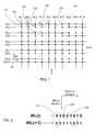
- FIG. 1is a schematic diagram of a portion of a memory array 100 , according to an embodiment.
- a memory devicemay comprise memory array 100 and address decoding circuitry (not shown) to read from or write to selected memory cells via bitlines or wordlines.
- Memory cells 150may be connected at intersections of wordlines and bitlines and may be selectively addressed by the wordlines or bitlines.
- memory cell 155may be programmed to be in a zero-bit state by placing a zero-bit on wordline WL 1 in a bitline BL 1 position.
- memory cell 157may be programmed to be in a one-bit state by placing a one-bit on wordline WL 2 in a bitline BL 1 position.
- FIG. 1shows wordline WL 3 with bits 0-1-0-1 in bitline positions BL 1 , BL 2 , BL 3 , and BL 4 , respectively.
- Memory cells 150may comprise PCM cells, though claimed subject matter is not so limited.
- adjacent wordlines in memory array 100may be physically spaced apart by two different distances.
- adjacent wordlines WL 9 and WL 10may be spaced apart by a distance D 1
- adjacent wordlines WL 8 and WL 9may be spaced apart by a distance D 2 .
- the different spacing distancesmay be determined, at least in part, from fabrication architecture of a semiconductor memory device that includes memory array 100 , for example.
- adjacent wordlinesmay be physically grouped in pairs with an inter-pair spacing of distance D 1 , whereas such pairs of wordlines may be spaced apart a distance D 2 . Referring to FIG.
- adjacent wordlines WL 1 and WL 2comprise a wordline pair separated by a distance D 1
- adjacent wordlines WL 3 and WL 4comprise a wordline pair separated by a distance D 1
- adjacent wordlines WL 5 and WL 6comprise a wordline pair separated by a distance D 1
- adjacent wordlines WL 7 and WL 8comprise a wordline pair separated by a distance D 1
- adjacent wordlines WL 9 and WL 10comprise a wordline pair separated by a distance D 1
- wordline WL 2 and wordline WL 3though they are adjacent to one another, may be separated by a distance D 2 , which may be greater than inter-pair spacing distance D 1 .
- wordline WL 4 and wordline WL 5may be separated by a distance D 2
- wordline WL 6 and wordline WL 7may be separated by a distance D 2
- wordline WL 8 and wordline WL 9may be separated by a distance D 2 .
- thermal contact among PCM cellsmay lead to a program-disturb event, wherein a state of one PCM cell may be disturbed by the state of a neighboring PCM cell.
- a neighboring PCM cell nearest the re-programmed PCM cellmay be affected more than other neighboring PCM cells.
- a neighboring PCM cell nearest the re-programmed PCM cellmay be located in a wordline adjacent to a wordline of the re-programmed PCM cell.
- a neighboring PCM cell located in a wordline adjacent to a wordline of the re-programmed PCM cellmay be program-disturbed by the re-programming process of the neighboring PCM cell.
- memory cells included in wordlines of a wordline pairmay be physically near one another so as to be affected by a program-disturb event. More specifically, memory cells included in wordlines of a wordline pair along a same bitline may be physically near enough to one another so as to be affected by a program-disturb event. On the other hand, memory cells included in wordlines of different wordline pairs, even if on a same bitline, may be physically separated enough so as to not be substantially affected by a program-disturb event.
- memory cells in memory cell pair 110may program-disturb one another, whereas memory cells in memory cell pair 120 need not program-disturb one another.
- PCM cells in a zero-bit, amorphous statemay be more susceptible to effects of a program-disturb event compared to PCM cells in a one-bit, crystalline state.
- memory cells in zero-bit states in memory cell pair 110may program-disturb one another, whereas memory cells 155 and 157 in zero-bit and one-bit states, respectively, need not program-disturb one another.
- PCM cells in adjacent wordlines of wordline pairsmay be more susceptible to effects of a program-disturb event compared to PCM cells in a same wordline and adjacent bitlines. Such effects may change a PCM memory cell in a zero-bit state to a one-bit state or vise versa.
- memory cells in memory cell pair 130need not program-disturb one another, even though the adjacent memory cells may both be in zero-bit states.
- a particular order of one-bits and zero-bits to be written to memory cells in two adjacent wordlinese.g., WL 1 and WL 2 , WL 3 and WL 4 , WL 5 and WL 6 , and so on
- two adjacent wordlinese.g., WL 1 and WL 2 , WL 3 and WL 4 , WL 5 and WL 6 , and so on
- one-bits in WL 1 and WL 2may be written before zero-bits in WL 1 and WL 2 .
- FIG. 2is a schematic diagram of an arrangement of program bits on adjacent wordlines, according to an embodiment.
- FIG. 2may depict a memory array similar to that of FIG. 1 , but without explicitly showing memory cells, wordlines, and bitlines.
- a wordline WL(i)(i comprises an integer) may have bits 0-1-0-0-1-0-1-0 on consecutive bitlines, such as BL 1 , BL 2 , BL 3 , and so on, shown in FIG. 1 .
- An adjacent wordline WL(i+1)may have bits 0-1-1-1-1-0-1-1 on the same consecutive bitlines as for WL(i).
- PCM cells in a zero-bit, amorphous statemay be more susceptible to effects of a program-disturb event compared to PCM cells in a one-bit, crystalline state.
- PCM cells in adjacent wordlinesmay be more susceptible to effects of a program-disturb event compared to PCM cells in a same wordline and adjacent bitlines.
- zero-bit pair 210comprising zero bits on a same bitline and adjacent wordlines WL(i) and WL(i+1), may lead to an undesirable program-disturb event.
- zero-bit pair 220comprising zero bits on a same bitline and adjacent wordlines WL(i) and WL(i+1), may also lead to an undesirable program-disturb event.
- zero-bit pair 230comprising zero bits on a same wordline WL(i) but adjacent bitlines, need not lead to a program-disturb event. Accordingly, as discussed above, it may be desirable to arrange a particular order of one-bits and zero-bits to be written to memory cells in two adjacent wordlines at a time.
- FIG. 3is a schematic diagram to show notation for describing bit locations of an arrangement of program bits on adjacent wordlines 305 and 310 , according to an embodiment.
- wordline 305may comprise a wordline WL(i)
- wordline 310may comprise a wordline WL(i+1), for an integer i, as in FIGS. 2 and 4 A- 4 D.
- bits of a wordlinemay be described, from left to write, as A 0 , A 1 , A 2 , and so on for one wordline, and B 0 , B 1 , B 2 , and so on for another (e.g., adjacent) wordline.
- a 0 , A 1 , A 2and so on for one wordline
- B 0 , B 1 , B 2and so on for another (e.g., adjacent) wordline.
- claimed subject matteris not limited in this respect.
- FIGS. 4A-4Dare schematic diagrams of an arrangement of program bits on adjacent wordlines of a memory array, according to an embodiment.
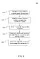
- FIG. 5is a flow diagram of an embodiment of a process 500 to program bits in a memory array, such as memory array 100 shown in FIG. 1 , for example.
- Process 500may comprise a technique to avoid or reduce a number of occurrences of program-disturb events.
- Process 500may be performed by a memory controller, for example.
- a desirable outcomefor example, is that, during a process of programming a memory array, adjacent wordlines along same bitlines will not both be programmed with a zero-bit and a one-bit at the same time, regardless of the combination or ordering of bits to be written to the wordlines.
- a group of bits to program into a memory arraymay be received.
- a processor or memory controllermay provide a group of bits to program into a memory array.
- a group of bitsmay comprise a byte, a word, or several to several hundred data bits, just to name a few examples.
- such a group of bitsmay comprise a first sequence of bits, such as 410 , and a second sequence of bits 420 .
- bits 410may be written to wordline WL(i) and bits 420 may be written to wordline WL(i+1).
- FIG. 4Ashows bits to be written to wordlines WL(i) and WL(i+1) in this particular example, while FIGS. 4B-4D show a process for writing the bits.
- a buffermay comprise a program buffer that may be included in a memory device that also includes the memory array.
- Such a buffermay comprise memory to temporarily store a plurality of bits 410 and 420 during a process of writing the bits to two adjacent wordlines, such as WL(i) and WL(i+1). Bits 410 and 420 may be written to the two adjacent wordlines in a particular sequence based, at least in part, on whether the bits comprise one-bits or zero-bits.
- program bitsmay comprise a first group of bits 410 to be written to a wordline WL(i) and a second group of bits 420 to be written to a second adjacent wordline WL(i+1).
- first group 410may be written to wordline WL(i) before writing one-bits of second group 420 to adjacent wordline WL(i+1).
- one-bits A 1 and A 4may be written to wordline WL(i) and one-bits B 0 , B 3 , B 6 , and B 7 may be written to wordline WL(i+1).
- Remaining bits, comprising zero-bitsmay be written in a process described below.
- zero-bitsmay be written to the two wordlines in the following manner.
- Zero-bits of the first group of bits that are to be written to the first wordlinemay be written to memory cell locations that are immediately adjacent to one-bits of the adjacent second wordline. For example, referring to FIG. 4C , zero-bit A 0 on wordline WL(i) may be adjacent to one-bit B 0 on wordline WL(i+1). In other words, A 0 and B 0 may be on a same bit line.
- zero-bits of the second group of bits that are to be written to the second wordlinemay be written to memory cell locations that are immediately adjacent to one-bits of the adjacent first wordline.
- zero-bit B 1 on wordline WL(i+1)may be adjacent to one-bit A 1 on wordline WL(i);
- zero-bit A 3 on wordline WL(i)may be adjacent to one-bit B 3 on wordline WL(i+1);
- zero-bit B 4 on wordline WL(i+1)may be adjacent to one-bit A 4 on wordline WL(i);
- zero-bit A 6 on wordline WL(i)may be adjacent to one-bit B 6 on wordline WL(i+1);
- zero-bit A 7 on wordline WL(i)may be adjacent to one-bit B 7 on wordline WL(i+1).
- zero-bitsmay be written to the first wordline WL(i) while simultaneously writing zero-bits to the second wordline WL(i+1).
- a portion of process 500 comprising block 540need not be performed so that process 500 may proceed from block 530 to block 550 , for example.
- zero-bits A 2 and A 5may be written to the first wordline WL(i) while simultaneously writing zero-bits B 2 and B 5 to the second wordline WL(i+1).
- block 540is not performed, zero-bits A 0 , A 2 , A 3 , A 5 , A 6 , and A 7 may be written to the first wordline WL(i) while simultaneously writing zero-bits B 1 , B 2 , B 4 , and B 5 to the second wordline WL(i+1).
- Process 500merely describes an example of a programming embodiment, but other programming techniques may be used. Also, various portions or details of process 500 may be changed. Accordingly, details of process 500 are merely examples, and claimed subject matter is not so limited.
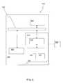
- FIG. 6is a schematic diagram illustrating an embodiment of a computing system 600 including a memory device 610 .
- a computing devicemay comprise one or more processors, for example, to execute an application or other code.
- memory device 610may comprise memory array 100 , shown in FIG. 1 .
- a computing device 604may be representative of any device, appliance, or machine that may be configurable to manage memory device 610 .
- Memory device 610may include a memory controller 615 and a memory 622 , which may comprise PCM, for example.
- computing device 604may include: one or more computing devices or platforms, such as, e.g., a desktop computer, a laptop computer, a workstation, a server device, or the like; one or more personal computing or communication devices or appliances, such as, e.g., a personal digital assistant, mobile communication device, or the like; a computing system or associated service provider capability, such as, e.g., a database or information storage service provider/system; or any combination thereof. It is recognized that all or part of the various devices shown in system 600 , and the processes and methods as further described herein, may be implemented using or otherwise including hardware, firmware, software, or any combination thereof.
- computing device 604may include at least one processing unit 620 that is operatively coupled to memory 622 through a bus 640 and a host or memory controller 615 .
- Processing unit 620is representative of one or more circuits configurable to perform at least a portion of an information computing procedure or process.
- processing unit 620may include one or more processors, controllers, microprocessors, microcontrollers, application specific integrated circuits, digital signal processors, programmable logic devices, field programmable gate arrays, and the like, or any combination thereof.
- Processing unit 620may include an operating system configured to communicate with memory controller 615 . Such an operating system may, for example, generate commands to be sent to memory controller 615 over bus 640 . Such commands may comprise read or write commands.
- memory controller 615may arrange program bits into a buffer so as to write the bits to two adjacent wordlines at a time, and may write one-bits to the two adjacent wordlines before writing zero-bits to the two adjacent wordlines.
- memory controller 615may arrange program bits into a buffer so as to write the bits to two adjacent wordlines at a time, and may write one-bits to the two adjacent wordlines before writing zero-bits to the two adjacent wordlines.
- Memory 622is representative of any information storage mechanism.
- Memory 622may include, for example, a primary memory 624 or a secondary memory 626 .
- Primary memory 624may include, for example, a random access memory, read only memory, etc. While illustrated in this example as being separate from processing unit 620 , it should be understood that all or part of primary memory 624 may be provided within or otherwise co-located/coupled with processing unit 620 .
- Secondary memory 626may include, for example, the same or similar type of memory as primary memory or one or more information storage devices or systems, such as, for example, a disk drive, an optical disc drive, a tape drive, a solid state memory drive, etc.
- secondary memory 626may be operatively receptive of, or otherwise configurable to couple to, a computer-readable medium 628 .
- Computer-readable medium 628may include, for example, any medium that can carry or make accessible information, code, or instructions for one or more of the devices in system 600 .
- Computing device 604may include, for example, an input/output 632 .
- Input/output 632is representative of one or more devices or features that may be configurable to accept or otherwise introduce human or machine inputs, or one or more devices or features that may be configurable to deliver or otherwise provide for human or machine outputs.
- input/output device 632may include an operatively configured display, speaker, keyboard, mouse, trackball, touch screen, data port, etc.
- claimed subject matteris not limited in scope to a particular embodiment or implementation.
- one embodimentmay be in hardware, such as implemented on a device or combination of devices, for example.
- one embodimentmay comprise one or more articles, such as a storage medium or storage media that may have stored thereon instructions capable of being executed by a specific or special purpose system or apparatus, for example, to lead to performance of an embodiment of a method in accordance with claimed subject matter, such as one of the embodiments previously described, for example.
- claimed subject matteris, of course, not limited to one of the embodiments described necessarily.
- a specific or special purpose computing platformmay include one or more processing units or processors, one or more input/output devices, such as a display, a keyboard or a mouse, or one or more memories, such as static random access memory, dynamic random access memory, flash memory, or a hard drive, although, again, claimed subject matter is not limited in scope to this example.
Landscapes
- Engineering & Computer Science (AREA)
- Theoretical Computer Science (AREA)
- Physics & Mathematics (AREA)
- General Engineering & Computer Science (AREA)
- General Physics & Mathematics (AREA)
- Chemical & Material Sciences (AREA)
- Crystallography & Structural Chemistry (AREA)
- Microelectronics & Electronic Packaging (AREA)
- Read Only Memory (AREA)
Abstract
Description
Claims (20)
Priority Applications (2)
| Application Number | Priority Date | Filing Date | Title |
|---|---|---|---|
| US13/457,799US9105314B2 (en) | 2012-04-27 | 2012-04-27 | Program-disturb decoupling for adjacent wordlines of a memory device |
| US14/807,796US9336843B2 (en) | 2012-04-27 | 2015-07-23 | Program-disturb decoupling for adjacent wordlines of a memory device |
Applications Claiming Priority (1)
| Application Number | Priority Date | Filing Date | Title |
|---|---|---|---|
| US13/457,799US9105314B2 (en) | 2012-04-27 | 2012-04-27 | Program-disturb decoupling for adjacent wordlines of a memory device |
Related Child Applications (1)
| Application Number | Title | Priority Date | Filing Date |
|---|---|---|---|
| US14/807,796ContinuationUS9336843B2 (en) | 2012-04-27 | 2015-07-23 | Program-disturb decoupling for adjacent wordlines of a memory device |
Publications (2)
| Publication Number | Publication Date |
|---|---|
| US20130290604A1 US20130290604A1 (en) | 2013-10-31 |
| US9105314B2true US9105314B2 (en) | 2015-08-11 |
Family
ID=49478384
Family Applications (2)
| Application Number | Title | Priority Date | Filing Date |
|---|---|---|---|
| US13/457,799Active2034-01-01US9105314B2 (en) | 2012-04-27 | 2012-04-27 | Program-disturb decoupling for adjacent wordlines of a memory device |
| US14/807,796ActiveUS9336843B2 (en) | 2012-04-27 | 2015-07-23 | Program-disturb decoupling for adjacent wordlines of a memory device |
Family Applications After (1)
| Application Number | Title | Priority Date | Filing Date |
|---|---|---|---|
| US14/807,796ActiveUS9336843B2 (en) | 2012-04-27 | 2015-07-23 | Program-disturb decoupling for adjacent wordlines of a memory device |
Country Status (1)
| Country | Link |
|---|---|
| US (2) | US9105314B2 (en) |
Cited By (2)
| Publication number | Priority date | Publication date | Assignee | Title |
|---|---|---|---|---|
| US9336843B2 (en) | 2012-04-27 | 2016-05-10 | Micron Technology, Inc. | Program-disturb decoupling for adjacent wordlines of a memory device |
| US9721639B1 (en) | 2016-06-21 | 2017-08-01 | Micron Technology, Inc. | Memory cell imprint avoidance |
Families Citing this family (5)
| Publication number | Priority date | Publication date | Assignee | Title |
|---|---|---|---|---|
| US8467237B2 (en) | 2010-10-15 | 2013-06-18 | Micron Technology, Inc. | Read distribution management for phase change memory |
| US9001575B2 (en) | 2012-03-30 | 2015-04-07 | Micron Technology, Inc. | Encoding program bits to decouple adjacent wordlines in a memory device |
| US8910000B2 (en) | 2012-05-17 | 2014-12-09 | Micron Technology, Inc. | Program-disturb management for phase change memory |
| US10157650B1 (en) | 2017-07-26 | 2018-12-18 | Micron Technology, Inc. | Program operations in memory |
| US12009027B2 (en) | 2021-12-23 | 2024-06-11 | Micron Technology, Inc. | Refresh of neighboring memory cells based on read status |
Citations (32)
| Publication number | Priority date | Publication date | Assignee | Title |
|---|---|---|---|---|
| US20040225705A1 (en) | 2003-03-28 | 2004-11-11 | Dmitriy Rumynin | Method and device for performing operations involving multiplication of selectively partitioned binary inputs using booth encoding |
| US20060123288A1 (en) | 2004-11-19 | 2006-06-08 | Fong Luk | Generation of test vectors for testing electronic circuits taking into account of defect probability |
| US20070255891A1 (en)* | 2004-04-05 | 2007-11-01 | Super Talent Electronics Inc. | High-Speed Controller for Phase-Change Memory Peripheral Device |
| US7352605B2 (en)* | 2005-10-24 | 2008-04-01 | Hynix Semiconductor Inc. | Nonvolatile ferroelectric memory device and method thereof |
| US20080084773A1 (en) | 2006-10-04 | 2008-04-10 | Texas Instruments Incorporated | Methods and systems for accessing memory |
| US20080158948A1 (en) | 2006-12-31 | 2008-07-03 | Sandisk Il Ltd. | Avoiding errors in a flash memory by using substitution transformations |
| WO2008085254A1 (en) | 2006-12-28 | 2008-07-17 | Micron Technology, Inc. | Non-volatile multilevel memory cell programming |
| US20100020615A1 (en) | 1995-01-31 | 2010-01-28 | Hitoshi Miwa | Clock synchronized non-volatile memory device |
| US20100265764A1 (en) | 2009-04-17 | 2010-10-21 | Samsung Electronics Co., Ltd. | Methods of accessing storage devices |
| US7952922B2 (en) | 2006-06-06 | 2011-05-31 | Micron Technology, Inc. | Method for programming a non-volatile memory device to reduce floating-gate-to-floating-gate coupling effect |
| US8031526B1 (en) | 2007-08-23 | 2011-10-04 | Marvell International Ltd. | Write pre-compensation for nonvolatile memory |
| US8050086B2 (en) | 2006-05-12 | 2011-11-01 | Anobit Technologies Ltd. | Distortion estimation and cancellation in memory devices |
| US8144505B2 (en) | 2008-07-11 | 2012-03-27 | Samsung Electronics Co., Ltd. | Nonvolatile memory devices supporting memory cells having different bit storage levels and methods of operating the same |
| US8169825B1 (en) | 2008-09-02 | 2012-05-01 | Anobit Technologies Ltd. | Reliable data storage in analog memory cells subjected to long retention periods |
| US20120127801A1 (en) | 2009-01-29 | 2012-05-24 | Ki Seog Kim | Method of operating nonvolatile memory device |
| US8228701B2 (en) | 2009-03-01 | 2012-07-24 | Apple Inc. | Selective activation of programming schemes in analog memory cell arrays |
| US20120195118A1 (en) | 2011-01-31 | 2012-08-02 | Hynix Semiconductor Inc. | Semiconductor memory apparatus, data programming method thereof, and memory system including the same |
| US8238157B1 (en) | 2009-04-12 | 2012-08-07 | Apple Inc. | Selective re-programming of analog memory cells |
| US8300478B2 (en) | 2007-09-19 | 2012-10-30 | Apple Inc. | Reducing distortion using joint storage |
| US20120290897A1 (en) | 2011-05-11 | 2012-11-15 | Samsung Electronics Co., Ltd. | Data storage system having multi-bit memory device and on-chip buffer program method thereof |
| US8335107B2 (en) | 2009-12-17 | 2012-12-18 | Hynix Semiconductor Inc. | Semiconductor memory device and method of operating the same |
| US20130007353A1 (en) | 2010-02-17 | 2013-01-03 | Sunil Shim | Control method of nonvolatile memory device |
| US8391062B2 (en) | 2009-06-22 | 2013-03-05 | Samsung Electronics Co., Ltd. | Nonvolatile memory device and related method of programming |
| US8437185B2 (en) | 2007-09-19 | 2013-05-07 | Apple Inc. | Programming orders for reducing distortion based on neighboring rows |
| US20130141972A1 (en) | 2010-03-09 | 2013-06-06 | Sangyong Yoon | Data storage system having multi-bit memory device and operating method thereof |
| US20130167251A1 (en) | 2010-11-18 | 2013-06-27 | Micron Technology, Inc. | Method of using memory instruction including parameter to affect operating condition of memory |
| US20130235665A1 (en) | 2007-06-19 | 2013-09-12 | Micron Technology, Inc. | Method and system for programming non-volatile memory cells based on programming of proximate memory cells |
| US20130262743A1 (en) | 2012-03-30 | 2013-10-03 | Micron Technology, Inc. | Encoding program bits to decouple adjacent wordlines in a memory device |
| US20130279260A1 (en) | 2010-08-16 | 2013-10-24 | Samsung Electronics Co., Ltd. | Non-volatile memory device and method for programming the device, and memory system |
| US20130311837A1 (en) | 2012-05-17 | 2013-11-21 | Micron Technology, Inc. | Program-disturb management for phase change memory |
| US8593873B2 (en) | 2011-08-26 | 2013-11-26 | Micron Technology, Inc. | Apparatuses and methods of reprogramming memory cells |
| US8743622B2 (en) | 2012-01-13 | 2014-06-03 | Micron Technology, Inc. | Memory devices and programming methods that program a memory cell with a data value, read the data value from the memory cell and reprogram the memory cell with the read data value |
Family Cites Families (16)
| Publication number | Priority date | Publication date | Assignee | Title |
|---|---|---|---|---|
| US6868025B2 (en) | 2003-03-10 | 2005-03-15 | Sharp Laboratories Of America, Inc. | Temperature compensated RRAM circuit |
| WO2004090984A1 (en)* | 2003-04-03 | 2004-10-21 | Kabushiki Kaisha Toshiba | Phase change memory device |
| EP1699054A1 (en) | 2005-03-03 | 2006-09-06 | STMicroelectronics S.r.l. | A memory device with a ramp-like voltage biasing structure and reduced number of reference cells |
| US7495944B2 (en) | 2005-03-30 | 2009-02-24 | Ovonyx, Inc. | Reading phase change memories |
| KR101367659B1 (en) | 2007-07-12 | 2014-02-25 | 삼성전자주식회사 | Multi-level phase change memory device for reducing read error and read method thereof |
| CN101471130B (en) | 2007-12-25 | 2011-08-24 | 财团法人工业技术研究院 | Phase change memory and control method of phase change memory |
| US7787282B2 (en) | 2008-03-21 | 2010-08-31 | Micron Technology, Inc. | Sensing resistance variable memory |
| US8027187B2 (en) | 2008-09-12 | 2011-09-27 | Micron Technology, Inc. | Memory sensing devices, methods, and systems |
| WO2010076834A1 (en) | 2008-12-31 | 2010-07-08 | Ferdinando Bedeschi | Reliable set operation for phase-change memory cell |
| KR101094904B1 (en) | 2009-09-30 | 2011-12-15 | 주식회사 하이닉스반도체 | Reference voltage generation circuit and method, phase change memory device and read method using same |
| TWI375224B (en) | 2009-11-20 | 2012-10-21 | Ind Tech Res Inst | Voltage compensation circuit, multi-level memory device with the same, and voltage compensation method for reading the multi-level memory device |
| CN101699562B (en) | 2009-11-23 | 2012-10-10 | 中国科学院上海微系统与信息技术研究所 | Erasing method of phase change memory |
| KR20110099570A (en) | 2010-03-02 | 2011-09-08 | 삼성전자주식회사 | Nonvolatile Memory Device, Its Program Method, And Memory System Including It |
| US8467237B2 (en) | 2010-10-15 | 2013-06-18 | Micron Technology, Inc. | Read distribution management for phase change memory |
| KR20130033018A (en)* | 2011-09-26 | 2013-04-03 | 에스케이하이닉스 주식회사 | Semiconductor integrated circuit system being able to decrease distubance and method for driving the same |
| US9105314B2 (en) | 2012-04-27 | 2015-08-11 | Micron Technology, Inc. | Program-disturb decoupling for adjacent wordlines of a memory device |
- 2012
- 2012-04-27USUS13/457,799patent/US9105314B2/enactiveActive
- 2015
- 2015-07-23USUS14/807,796patent/US9336843B2/enactiveActive
Patent Citations (50)
| Publication number | Priority date | Publication date | Assignee | Title |
|---|---|---|---|---|
| US20100020615A1 (en) | 1995-01-31 | 2010-01-28 | Hitoshi Miwa | Clock synchronized non-volatile memory device |
| US7308471B2 (en) | 2003-03-28 | 2007-12-11 | Arithmatica Limited | Method and device for performing operations involving multiplication of selectively partitioned binary inputs using booth encoding |
| US20040225705A1 (en) | 2003-03-28 | 2004-11-11 | Dmitriy Rumynin | Method and device for performing operations involving multiplication of selectively partitioned binary inputs using booth encoding |
| US20070255891A1 (en)* | 2004-04-05 | 2007-11-01 | Super Talent Electronics Inc. | High-Speed Controller for Phase-Change Memory Peripheral Device |
| US20060123288A1 (en) | 2004-11-19 | 2006-06-08 | Fong Luk | Generation of test vectors for testing electronic circuits taking into account of defect probability |
| US7266741B2 (en) | 2004-11-19 | 2007-09-04 | Fong Luk | Generation of test vectors for testing electronic circuits taking into account of defect probability |
| US7352605B2 (en)* | 2005-10-24 | 2008-04-01 | Hynix Semiconductor Inc. | Nonvolatile ferroelectric memory device and method thereof |
| US8570804B2 (en) | 2006-05-12 | 2013-10-29 | Apple Inc. | Distortion estimation and cancellation in memory devices |
| US8050086B2 (en) | 2006-05-12 | 2011-11-01 | Anobit Technologies Ltd. | Distortion estimation and cancellation in memory devices |
| US7952922B2 (en) | 2006-06-06 | 2011-05-31 | Micron Technology, Inc. | Method for programming a non-volatile memory device to reduce floating-gate-to-floating-gate coupling effect |
| US8462548B2 (en) | 2006-06-06 | 2013-06-11 | Micron Technology, Inc. | Non-volatile memory device capable of reducing floating gate-to-floating gate coupling effect during programming |
| US7630257B2 (en) | 2006-10-04 | 2009-12-08 | Texas Instruments Incorporated | Methods and systems for accessing memory |
| US20080084773A1 (en) | 2006-10-04 | 2008-04-10 | Texas Instruments Incorporated | Methods and systems for accessing memory |
| WO2008085254A1 (en) | 2006-12-28 | 2008-07-17 | Micron Technology, Inc. | Non-volatile multilevel memory cell programming |
| US7701765B2 (en) | 2006-12-28 | 2010-04-20 | Micron Technology, Inc. | Non-volatile multilevel memory cell programming |
| US8369147B2 (en) | 2006-12-28 | 2013-02-05 | Micron Technology, Inc. | Non-volatile multilevel memory cell programming |
| US7984360B2 (en) | 2006-12-31 | 2011-07-19 | Ramot At Tel Aviv University Ltd. | Avoiding errors in a flash memory by using substitution transformations |
| US20080158948A1 (en) | 2006-12-31 | 2008-07-03 | Sandisk Il Ltd. | Avoiding errors in a flash memory by using substitution transformations |
| US20130235665A1 (en) | 2007-06-19 | 2013-09-12 | Micron Technology, Inc. | Method and system for programming non-volatile memory cells based on programming of proximate memory cells |
| US8031526B1 (en) | 2007-08-23 | 2011-10-04 | Marvell International Ltd. | Write pre-compensation for nonvolatile memory |
| US8437185B2 (en) | 2007-09-19 | 2013-05-07 | Apple Inc. | Programming orders for reducing distortion based on neighboring rows |
| US8300478B2 (en) | 2007-09-19 | 2012-10-30 | Apple Inc. | Reducing distortion using joint storage |
| US8144505B2 (en) | 2008-07-11 | 2012-03-27 | Samsung Electronics Co., Ltd. | Nonvolatile memory devices supporting memory cells having different bit storage levels and methods of operating the same |
| US8169825B1 (en) | 2008-09-02 | 2012-05-01 | Anobit Technologies Ltd. | Reliable data storage in analog memory cells subjected to long retention periods |
| US20120127801A1 (en) | 2009-01-29 | 2012-05-24 | Ki Seog Kim | Method of operating nonvolatile memory device |
| US8767469B2 (en) | 2009-01-29 | 2014-07-01 | Hynix Semiconductor Inc. | Method of operating nonvolatile memory device |
| US20120262971A1 (en) | 2009-03-01 | 2012-10-18 | Dotan Sokolov | Selective Activation of Programming Schemes in Analog Memory Cell Arrays |
| US20120262970A1 (en) | 2009-03-01 | 2012-10-18 | Dotan Sokolov | Selective activation of programming schemes in analog memory cell arrays |
| US8228701B2 (en) | 2009-03-01 | 2012-07-24 | Apple Inc. | Selective activation of programming schemes in analog memory cell arrays |
| US8717792B2 (en) | 2009-03-01 | 2014-05-06 | Apple Inc. | Selective activation of programming schemes in analog memory cell arrays |
| US8238157B1 (en) | 2009-04-12 | 2012-08-07 | Apple Inc. | Selective re-programming of analog memory cells |
| US20120268990A1 (en) | 2009-04-12 | 2012-10-25 | Naftali Sommer | Selective re-programming of analog memory cells |
| US8310876B2 (en) | 2009-04-17 | 2012-11-13 | Samsung Electronics Co., Ltd. | Methods of accessing storage devices |
| US20100265764A1 (en) | 2009-04-17 | 2010-10-21 | Samsung Electronics Co., Ltd. | Methods of accessing storage devices |
| US8391062B2 (en) | 2009-06-22 | 2013-03-05 | Samsung Electronics Co., Ltd. | Nonvolatile memory device and related method of programming |
| US20130141974A1 (en) | 2009-06-22 | 2013-06-06 | Samsung Electronics Co., Ltd. | Nonvolatile memory device and related method of programming |
| US8681543B2 (en) | 2009-06-22 | 2014-03-25 | Samsung Electronics Co., Ltd. | Nonvolatile memory device and related method of programming |
| US8335107B2 (en) | 2009-12-17 | 2012-12-18 | Hynix Semiconductor Inc. | Semiconductor memory device and method of operating the same |
| US20130007353A1 (en) | 2010-02-17 | 2013-01-03 | Sunil Shim | Control method of nonvolatile memory device |
| US20130141972A1 (en) | 2010-03-09 | 2013-06-06 | Sangyong Yoon | Data storage system having multi-bit memory device and operating method thereof |
| US8693247B2 (en) | 2010-08-16 | 2014-04-08 | Samsung Electronics Co., Ltd. | Non-volatile memory device and method for programming the device, and memory system |
| US20130279260A1 (en) | 2010-08-16 | 2013-10-24 | Samsung Electronics Co., Ltd. | Non-volatile memory device and method for programming the device, and memory system |
| US20130167251A1 (en) | 2010-11-18 | 2013-06-27 | Micron Technology, Inc. | Method of using memory instruction including parameter to affect operating condition of memory |
| US20120195118A1 (en) | 2011-01-31 | 2012-08-02 | Hynix Semiconductor Inc. | Semiconductor memory apparatus, data programming method thereof, and memory system including the same |
| US20120290897A1 (en) | 2011-05-11 | 2012-11-15 | Samsung Electronics Co., Ltd. | Data storage system having multi-bit memory device and on-chip buffer program method thereof |
| US8593873B2 (en) | 2011-08-26 | 2013-11-26 | Micron Technology, Inc. | Apparatuses and methods of reprogramming memory cells |
| US8743622B2 (en) | 2012-01-13 | 2014-06-03 | Micron Technology, Inc. | Memory devices and programming methods that program a memory cell with a data value, read the data value from the memory cell and reprogram the memory cell with the read data value |
| US20130262743A1 (en) | 2012-03-30 | 2013-10-03 | Micron Technology, Inc. | Encoding program bits to decouple adjacent wordlines in a memory device |
| US20130311837A1 (en) | 2012-05-17 | 2013-11-21 | Micron Technology, Inc. | Program-disturb management for phase change memory |
| US8910000B2 (en) | 2012-05-17 | 2014-12-09 | Micron Technology, Inc. | Program-disturb management for phase change memory |
Non-Patent Citations (1)
| Title |
|---|
| Patent Application titled "Encoding Program Bits to Decouple Adjacent Wordlines in a Memory Device," U.S. Appl. No. 13/435,243, filed Mar. 30, 2012, 24 Pages. |
Cited By (6)
| Publication number | Priority date | Publication date | Assignee | Title |
|---|---|---|---|---|
| US9336843B2 (en) | 2012-04-27 | 2016-05-10 | Micron Technology, Inc. | Program-disturb decoupling for adjacent wordlines of a memory device |
| US9721639B1 (en) | 2016-06-21 | 2017-08-01 | Micron Technology, Inc. | Memory cell imprint avoidance |
| US10083732B2 (en) | 2016-06-21 | 2018-09-25 | Micron Technology, Inc. | Memory cell imprint avoidance |
| US10475500B2 (en) | 2016-06-21 | 2019-11-12 | Micron Technology, Inc. | Memory cell imprint avoidance |
| US10978128B2 (en) | 2016-06-21 | 2021-04-13 | Micron Technology, Inc. | Memory cell imprint avoidance |
| US11501817B2 (en) | 2016-06-21 | 2022-11-15 | Micron Technology, Inc. | Memory cell imprint avoidance |
Also Published As
| Publication number | Publication date |
|---|---|
| US20150325293A1 (en) | 2015-11-12 |
| US9336843B2 (en) | 2016-05-10 |
| US20130290604A1 (en) | 2013-10-31 |
Similar Documents
| Publication | Publication Date | Title |
|---|---|---|
| US9336843B2 (en) | Program-disturb decoupling for adjacent wordlines of a memory device | |
| US9508426B2 (en) | Program-disturb management for phase change memory | |
| US10430108B2 (en) | Concurrent copying of first and second subsets of pages from media such as SLC NAND to media such as QLC or MLC NAND for completion of copying of data | |
| US8451662B2 (en) | Reading memory cell history during program operation for adaptive programming | |
| US20190214078A1 (en) | Method of operating resistive memory device reducing read disturbance | |
| US8036016B2 (en) | Maintenance process to enhance memory endurance | |
| US8675423B2 (en) | Apparatuses and methods including supply current in memory | |
| US9342447B2 (en) | Data storage system and method of operating data storage system | |
| US9001575B2 (en) | Encoding program bits to decouple adjacent wordlines in a memory device | |
| US10388367B2 (en) | Nonvolatile memory device with controlled word line setup time | |
| US10163502B2 (en) | Selective performance level modes of operation in a non-volatile memory | |
| US9164894B2 (en) | Staggered programming for resistive memories | |
| US9299429B2 (en) | Nonvolatile memory device using a resistance material and a driving method thereof | |
| US20140247646A1 (en) | Nonvolatile memory device having multiple read circuits and using variable resistive materials | |
| US11404105B2 (en) | Write disturb refresh rate reduction using write history buffer | |
| CN109727618A (en) | Semiconductor memory system with resistance variable memory device and method of driving the same | |
| US8184487B2 (en) | Modified read operation for non-volatile memory | |
| US8971105B2 (en) | Methods and apparatuses for controlling memory write sequences | |
| US10854288B2 (en) | Semiconductor memory apparatus for preventing disturbance | |
| US12361979B2 (en) | Technologies for on-memory die voltage regulator | |
| CN112242154B (en) | Non-volatile storage device for mitigating interference and method of operating the same | |
| EP4109452B1 (en) | Technologies for burst memory write operations | |
| US12443362B2 (en) | Technologies for burst memory write operations | |
| US20230267988A1 (en) | Apparatus, method and system to reduce memory window latency and read disturb in a memory device for memory operations | |
| US20230307043A1 (en) | Technologies for current biasing for memory cells |
Legal Events
| Date | Code | Title | Description |
|---|---|---|---|
| AS | Assignment | Owner name:MICRON TECHNOLOGY, INC., IDAHO Free format text:ASSIGNMENT OF ASSIGNORS INTEREST;ASSIGNOR:BEDESCHI, FERDINANDO;REEL/FRAME:028118/0276 Effective date:20120420 | |
| AS | Assignment | Owner name:TEXAS INSTRUMENTS INC., TEXAS Free format text:ASSIGNMENT OF ASSIGNORS INTEREST;ASSIGNORS:VEDANTHAM, RAMANUJA;VIJAYASANKAR, KUMARAN;DABAK, ANAND;AND OTHERS;SIGNING DATES FROM 20120426 TO 20120427;REEL/FRAME:028170/0437 | |
| FEPP | Fee payment procedure | Free format text:PAYOR NUMBER ASSIGNED (ORIGINAL EVENT CODE: ASPN); ENTITY STATUS OF PATENT OWNER: LARGE ENTITY | |
| STCF | Information on status: patent grant | Free format text:PATENTED CASE | |
| AS | Assignment | Owner name:U.S. BANK NATIONAL ASSOCIATION, AS COLLATERAL AGENT, CALIFORNIA Free format text:SECURITY INTEREST;ASSIGNOR:MICRON TECHNOLOGY, INC.;REEL/FRAME:038669/0001 Effective date:20160426 Owner name:U.S. BANK NATIONAL ASSOCIATION, AS COLLATERAL AGEN Free format text:SECURITY INTEREST;ASSIGNOR:MICRON TECHNOLOGY, INC.;REEL/FRAME:038669/0001 Effective date:20160426 | |
| AS | Assignment | Owner name:MORGAN STANLEY SENIOR FUNDING, INC., AS COLLATERAL AGENT, MARYLAND Free format text:PATENT SECURITY AGREEMENT;ASSIGNOR:MICRON TECHNOLOGY, INC.;REEL/FRAME:038954/0001 Effective date:20160426 Owner name:MORGAN STANLEY SENIOR FUNDING, INC., AS COLLATERAL Free format text:PATENT SECURITY AGREEMENT;ASSIGNOR:MICRON TECHNOLOGY, INC.;REEL/FRAME:038954/0001 Effective date:20160426 | |
| AS | Assignment | Owner name:U.S. BANK NATIONAL ASSOCIATION, AS COLLATERAL AGENT, CALIFORNIA Free format text:CORRECTIVE ASSIGNMENT TO CORRECT THE REPLACE ERRONEOUSLY FILED PATENT #7358718 WITH THE CORRECT PATENT #7358178 PREVIOUSLY RECORDED ON REEL 038669 FRAME 0001. ASSIGNOR(S) HEREBY CONFIRMS THE SECURITY INTEREST;ASSIGNOR:MICRON TECHNOLOGY, INC.;REEL/FRAME:043079/0001 Effective date:20160426 Owner name:U.S. BANK NATIONAL ASSOCIATION, AS COLLATERAL AGEN Free format text:CORRECTIVE ASSIGNMENT TO CORRECT THE REPLACE ERRONEOUSLY FILED PATENT #7358718 WITH THE CORRECT PATENT #7358178 PREVIOUSLY RECORDED ON REEL 038669 FRAME 0001. ASSIGNOR(S) HEREBY CONFIRMS THE SECURITY INTEREST;ASSIGNOR:MICRON TECHNOLOGY, INC.;REEL/FRAME:043079/0001 Effective date:20160426 | |
| AS | Assignment | Owner name:JPMORGAN CHASE BANK, N.A., AS COLLATERAL AGENT, ILLINOIS Free format text:SECURITY INTEREST;ASSIGNORS:MICRON TECHNOLOGY, INC.;MICRON SEMICONDUCTOR PRODUCTS, INC.;REEL/FRAME:047540/0001 Effective date:20180703 Owner name:JPMORGAN CHASE BANK, N.A., AS COLLATERAL AGENT, IL Free format text:SECURITY INTEREST;ASSIGNORS:MICRON TECHNOLOGY, INC.;MICRON SEMICONDUCTOR PRODUCTS, INC.;REEL/FRAME:047540/0001 Effective date:20180703 | |
| AS | Assignment | Owner name:MICRON TECHNOLOGY, INC., IDAHO Free format text:RELEASE BY SECURED PARTY;ASSIGNOR:U.S. BANK NATIONAL ASSOCIATION, AS COLLATERAL AGENT;REEL/FRAME:047243/0001 Effective date:20180629 | |
| MAFP | Maintenance fee payment | Free format text:PAYMENT OF MAINTENANCE FEE, 4TH YEAR, LARGE ENTITY (ORIGINAL EVENT CODE: M1551); ENTITY STATUS OF PATENT OWNER: LARGE ENTITY Year of fee payment:4 | |
| AS | Assignment | Owner name:MICRON TECHNOLOGY, INC., IDAHO Free format text:RELEASE BY SECURED PARTY;ASSIGNOR:MORGAN STANLEY SENIOR FUNDING, INC., AS COLLATERAL AGENT;REEL/FRAME:050937/0001 Effective date:20190731 | |
| AS | Assignment | Owner name:MICRON TECHNOLOGY, INC., IDAHO Free format text:RELEASE BY SECURED PARTY;ASSIGNOR:JPMORGAN CHASE BANK, N.A., AS COLLATERAL AGENT;REEL/FRAME:051028/0001 Effective date:20190731 Owner name:MICRON SEMICONDUCTOR PRODUCTS, INC., IDAHO Free format text:RELEASE BY SECURED PARTY;ASSIGNOR:JPMORGAN CHASE BANK, N.A., AS COLLATERAL AGENT;REEL/FRAME:051028/0001 Effective date:20190731 | |
| MAFP | Maintenance fee payment | Free format text:PAYMENT OF MAINTENANCE FEE, 8TH YEAR, LARGE ENTITY (ORIGINAL EVENT CODE: M1552); ENTITY STATUS OF PATENT OWNER: LARGE ENTITY Year of fee payment:8 |