US9102124B2 - Electrochromic window fabrication methods - Google Patents
Electrochromic window fabrication methodsDownload PDFInfo
- Publication number
- US9102124B2 US9102124B2US13/431,729US201213431729AUS9102124B2US 9102124 B2US9102124 B2US 9102124B2US 201213431729 AUS201213431729 AUS 201213431729AUS 9102124 B2US9102124 B2US 9102124B2
- Authority
- US
- United States
- Prior art keywords
- glass sheet
- glass
- panes
- electrochromic
- cutting
- Prior art date
- Legal status (The legal status is an assumption and is not a legal conclusion. Google has not performed a legal analysis and makes no representation as to the accuracy of the status listed.)
- Active
Links
- 238000000034methodMethods0.000titleclaimsabstractdescription79
- 238000004519manufacturing processMethods0.000titleclaimsabstractdescription35
- 239000011521glassSubstances0.000claimsabstractdescription195
- 238000005520cutting processMethods0.000claimsabstractdescription80
- 239000005329float glassSubstances0.000claimsabstractdescription9
- 229920005989resinPolymers0.000claimsdescription34
- 239000011347resinSubstances0.000claimsdescription34
- 238000003475laminationMethods0.000claimsdescription26
- 230000003287optical effectEffects0.000claimsdescription20
- 238000000576coating methodMethods0.000claimsdescription15
- 239000007788liquidSubstances0.000claimsdescription12
- 230000003014reinforcing effectEffects0.000claimsdescription12
- 239000000758substrateSubstances0.000claimsdescription11
- 239000011248coating agentSubstances0.000claimsdescription9
- 238000005728strengtheningMethods0.000claimsdescription8
- 238000010030laminatingMethods0.000claimsdescription6
- 238000003698laser cuttingMethods0.000claimsdescription5
- VVQNEPGJFQJSBK-UHFFFAOYSA-NMethyl methacrylateChemical compoundCOC(=O)C(C)=CVVQNEPGJFQJSBK-UHFFFAOYSA-N0.000claimsdescription4
- 229920005372Plexiglas®Polymers0.000claimsdescription4
- 239000005341toughened glassSubstances0.000claimsdescription4
- NIXOWILDQLNWCW-UHFFFAOYSA-Nacrylic acid groupChemical groupC(C=C)(=O)ONIXOWILDQLNWCW-UHFFFAOYSA-N0.000claimsdescription2
- 239000003054catalystSubstances0.000claimsdescription2
- 239000005346heat strengthened glassSubstances0.000claims1
- 238000012217deletionMethods0.000abstractdescription26
- 230000037430deletionEffects0.000abstractdescription26
- 230000007547defectEffects0.000description60
- 230000008569processEffects0.000description31
- 239000000463materialSubstances0.000description21
- 238000000151depositionMethods0.000description17
- 230000008021depositionEffects0.000description14
- 230000004888barrier functionEffects0.000description12
- 238000009792diffusion processMethods0.000description12
- 238000013507mappingMethods0.000description12
- 230000000149penetrating effectEffects0.000description8
- 125000006850spacer groupChemical group0.000description7
- 230000008901benefitEffects0.000description6
- 230000015572biosynthetic processEffects0.000description6
- 238000007689inspectionMethods0.000description6
- 238000007789sealingMethods0.000description6
- 238000009966trimmingMethods0.000description5
- 230000008859changeEffects0.000description4
- 239000004020conductorSubstances0.000description4
- 238000000227grindingMethods0.000description4
- 238000010438heat treatmentMethods0.000description4
- 238000002955isolationMethods0.000description4
- 238000000059patterningMethods0.000description4
- 238000012360testing methodMethods0.000description4
- 230000003213activating effectEffects0.000description3
- 229910003460diamondInorganic materials0.000description3
- 239000010432diamondSubstances0.000description3
- 125000001475halogen functional groupChemical group0.000description3
- 230000010354integrationEffects0.000description3
- 238000003908quality control methodMethods0.000description3
- 239000007787solidSubstances0.000description3
- 238000005496temperingMethods0.000description3
- 230000000007visual effectEffects0.000description3
- XLYOFNOQVPJJNP-UHFFFAOYSA-NwaterSubstancesOXLYOFNOQVPJJNP-UHFFFAOYSA-N0.000description3
- XKRFYHLGVUSROY-UHFFFAOYSA-NArgonChemical compound[Ar]XKRFYHLGVUSROY-UHFFFAOYSA-N0.000description2
- 208000032750Device leakageDiseases0.000description2
- 241000282575GorillaSpecies0.000description2
- 238000002835absorbanceMethods0.000description2
- 230000003466anti-cipated effectEffects0.000description2
- 238000006243chemical reactionMethods0.000description2
- 238000004891communicationMethods0.000description2
- 238000007796conventional methodMethods0.000description2
- 238000001723curingMethods0.000description2
- 230000002950deficientEffects0.000description2
- 238000001514detection methodMethods0.000description2
- 239000007789gasSubstances0.000description2
- 238000010348incorporationMethods0.000description2
- 238000009434installationMethods0.000description2
- 239000002245particleSubstances0.000description2
- 229920003023plasticPolymers0.000description2
- 239000004033plasticSubstances0.000description2
- 229920002037poly(vinyl butyral) polymerPolymers0.000description2
- 238000012545processingMethods0.000description2
- 230000001681protective effectEffects0.000description2
- 230000009467reductionEffects0.000description2
- 239000000523sampleSubstances0.000description2
- 239000000126substanceSubstances0.000description2
- 238000001931thermographyMethods0.000description2
- 238000002834transmittanceMethods0.000description2
- DGAQECJNVWCQMB-PUAWFVPOSA-MIlexoside XXIXChemical compoundC[C@@H]1CC[C@@]2(CC[C@@]3(C(=CC[C@H]4[C@]3(CC[C@@H]5[C@@]4(CC[C@@H](C5(C)C)OS(=O)(=O)[O-])C)C)[C@@H]2[C@]1(C)O)C)C(=O)O[C@H]6[C@@H]([C@H]([C@@H]([C@H](O6)CO)O)O)O.[Na+]DGAQECJNVWCQMB-PUAWFVPOSA-M0.000description1
- BLRPTPMANUNPDV-UHFFFAOYSA-NSilaneChemical compound[SiH4]BLRPTPMANUNPDV-UHFFFAOYSA-N0.000description1
- 238000002679ablationMethods0.000description1
- 239000000654additiveSubstances0.000description1
- 239000000853adhesiveSubstances0.000description1
- 230000001070adhesive effectEffects0.000description1
- 229910001491alkali aluminosilicateInorganic materials0.000description1
- 150000001412aminesChemical class0.000description1
- 238000013459approachMethods0.000description1
- 229910052786argonInorganic materials0.000description1
- 230000009286beneficial effectEffects0.000description1
- 238000012512characterization methodMethods0.000description1
- 239000002800charge carrierSubstances0.000description1
- 239000003153chemical reaction reagentSubstances0.000description1
- 239000004927claySubstances0.000description1
- 239000003086colorantSubstances0.000description1
- 238000010276constructionMethods0.000description1
- 239000000356contaminantSubstances0.000description1
- 238000011109contaminationMethods0.000description1
- 238000001816coolingMethods0.000description1
- 239000002274desiccantSubstances0.000description1
- 230000001066destructive effectEffects0.000description1
- 238000010586diagramMethods0.000description1
- 239000000428dustSubstances0.000description1
- 239000000975dyeSubstances0.000description1
- 230000000694effectsEffects0.000description1
- 229920001971elastomerPolymers0.000description1
- 239000000806elastomerSubstances0.000description1
- 230000005611electricityEffects0.000description1
- 230000005670electromagnetic radiationEffects0.000description1
- 239000012776electronic materialSubstances0.000description1
- 238000005516engineering processMethods0.000description1
- 239000003822epoxy resinSubstances0.000description1
- 238000007730finishing processMethods0.000description1
- 239000005357flat glassSubstances0.000description1
- 238000013007heat curingMethods0.000description1
- 238000009863impact testMethods0.000description1
- 230000001976improved effectEffects0.000description1
- 230000001939inductive effectEffects0.000description1
- 239000011261inert gasSubstances0.000description1
- 239000012212insulatorSubstances0.000description1
- 150000002500ionsChemical class0.000description1
- 230000001788irregularEffects0.000description1
- 238000000608laser ablationMethods0.000description1
- 238000004093laser heatingMethods0.000description1
- 239000004973liquid crystal related substanceSubstances0.000description1
- 238000001459lithographyMethods0.000description1
- 230000007774longtermEffects0.000description1
- 238000010297mechanical methods and processMethods0.000description1
- 230000005226mechanical processes and functionsEffects0.000description1
- 230000001404mediated effectEffects0.000description1
- 229910052751metalInorganic materials0.000description1
- 239000002184metalSubstances0.000description1
- 230000000116mitigating effectEffects0.000description1
- 239000000203mixtureSubstances0.000description1
- 238000012986modificationMethods0.000description1
- 230000004048modificationEffects0.000description1
- QGLKJKCYBOYXKC-UHFFFAOYSA-NnonaoxidotritungstenChemical compoundO=[W]1(=O)O[W](=O)(=O)O[W](=O)(=O)O1QGLKJKCYBOYXKC-UHFFFAOYSA-N0.000description1
- 239000000049pigmentSubstances0.000description1
- 229920000647polyepoxidePolymers0.000description1
- 239000004848polyfunctional curativeSubstances0.000description1
- 238000003825pressingMethods0.000description1
- 230000005855radiationEffects0.000description1
- 238000002310reflectometryMethods0.000description1
- 230000002441reversible effectEffects0.000description1
- 238000005488sandblastingMethods0.000description1
- 238000012216screeningMethods0.000description1
- 239000000565sealantSubstances0.000description1
- 229910000077silaneInorganic materials0.000description1
- 238000005245sinteringMethods0.000description1
- 229910052708sodiumInorganic materials0.000description1
- 239000011734sodiumSubstances0.000description1
- 239000004575stoneSubstances0.000description1
- QHGNHLZPVBIIPX-UHFFFAOYSA-Ntin(ii) oxideChemical class[Sn]=OQHGNHLZPVBIIPX-UHFFFAOYSA-N0.000description1
- 230000007704transitionEffects0.000description1
- 229910001930tungsten oxideInorganic materials0.000description1
- ZNOKGRXACCSDPY-UHFFFAOYSA-Ntungsten trioxideChemical compoundO=[W](=O)=OZNOKGRXACCSDPY-UHFFFAOYSA-N0.000description1
- 238000009281ultraviolet germicidal irradiationMethods0.000description1
- 125000000391vinyl groupChemical group[H]C([*])=C([H])[H]0.000description1
- 229920002554vinyl polymerPolymers0.000description1
Images


Classifications
- B—PERFORMING OPERATIONS; TRANSPORTING
- B32—LAYERED PRODUCTS
- B32B—LAYERED PRODUCTS, i.e. PRODUCTS BUILT-UP OF STRATA OF FLAT OR NON-FLAT, e.g. CELLULAR OR HONEYCOMB, FORM
- B32B17/00—Layered products essentially comprising sheet glass, or glass, slag, or like fibres
- B32B17/06—Layered products essentially comprising sheet glass, or glass, slag, or like fibres comprising glass as the main or only constituent of a layer, next to another layer of a specific material
- B32B17/10—Layered products essentially comprising sheet glass, or glass, slag, or like fibres comprising glass as the main or only constituent of a layer, next to another layer of a specific material of synthetic resin
- B32B17/10005—Layered products essentially comprising sheet glass, or glass, slag, or like fibres comprising glass as the main or only constituent of a layer, next to another layer of a specific material of synthetic resin laminated safety glass or glazing
- B32B17/10009—Layered products essentially comprising sheet glass, or glass, slag, or like fibres comprising glass as the main or only constituent of a layer, next to another layer of a specific material of synthetic resin laminated safety glass or glazing characterized by the number, the constitution or treatment of glass sheets
- B32B17/10036—Layered products essentially comprising sheet glass, or glass, slag, or like fibres comprising glass as the main or only constituent of a layer, next to another layer of a specific material of synthetic resin laminated safety glass or glazing characterized by the number, the constitution or treatment of glass sheets comprising two outer glass sheets
- B32B17/10045—Layered products essentially comprising sheet glass, or glass, slag, or like fibres comprising glass as the main or only constituent of a layer, next to another layer of a specific material of synthetic resin laminated safety glass or glazing characterized by the number, the constitution or treatment of glass sheets comprising two outer glass sheets with at least one intermediate layer consisting of a glass sheet
- B32B17/10055—Layered products essentially comprising sheet glass, or glass, slag, or like fibres comprising glass as the main or only constituent of a layer, next to another layer of a specific material of synthetic resin laminated safety glass or glazing characterized by the number, the constitution or treatment of glass sheets comprising two outer glass sheets with at least one intermediate layer consisting of a glass sheet with at least one intermediate air space
- B—PERFORMING OPERATIONS; TRANSPORTING
- B32—LAYERED PRODUCTS
- B32B—LAYERED PRODUCTS, i.e. PRODUCTS BUILT-UP OF STRATA OF FLAT OR NON-FLAT, e.g. CELLULAR OR HONEYCOMB, FORM
- B32B17/00—Layered products essentially comprising sheet glass, or glass, slag, or like fibres
- B32B17/06—Layered products essentially comprising sheet glass, or glass, slag, or like fibres comprising glass as the main or only constituent of a layer, next to another layer of a specific material
- B32B17/10—Layered products essentially comprising sheet glass, or glass, slag, or like fibres comprising glass as the main or only constituent of a layer, next to another layer of a specific material of synthetic resin
- B32B17/10005—Layered products essentially comprising sheet glass, or glass, slag, or like fibres comprising glass as the main or only constituent of a layer, next to another layer of a specific material of synthetic resin laminated safety glass or glazing
- B32B17/10009—Layered products essentially comprising sheet glass, or glass, slag, or like fibres comprising glass as the main or only constituent of a layer, next to another layer of a specific material of synthetic resin laminated safety glass or glazing characterized by the number, the constitution or treatment of glass sheets
- B32B17/10128—Treatment of at least one glass sheet
- B—PERFORMING OPERATIONS; TRANSPORTING
- B32—LAYERED PRODUCTS
- B32B—LAYERED PRODUCTS, i.e. PRODUCTS BUILT-UP OF STRATA OF FLAT OR NON-FLAT, e.g. CELLULAR OR HONEYCOMB, FORM
- B32B17/00—Layered products essentially comprising sheet glass, or glass, slag, or like fibres
- B32B17/06—Layered products essentially comprising sheet glass, or glass, slag, or like fibres comprising glass as the main or only constituent of a layer, next to another layer of a specific material
- B32B17/10—Layered products essentially comprising sheet glass, or glass, slag, or like fibres comprising glass as the main or only constituent of a layer, next to another layer of a specific material of synthetic resin
- B32B17/10005—Layered products essentially comprising sheet glass, or glass, slag, or like fibres comprising glass as the main or only constituent of a layer, next to another layer of a specific material of synthetic resin laminated safety glass or glazing
- B32B17/10165—Functional features of the laminated safety glass or glazing
- B32B17/10174—Coatings of a metallic or dielectric material on a constituent layer of glass or polymer
- B32B17/10183—Coatings of a metallic or dielectric material on a constituent layer of glass or polymer being not continuous, e.g. in edge regions
- B—PERFORMING OPERATIONS; TRANSPORTING
- B32—LAYERED PRODUCTS
- B32B—LAYERED PRODUCTS, i.e. PRODUCTS BUILT-UP OF STRATA OF FLAT OR NON-FLAT, e.g. CELLULAR OR HONEYCOMB, FORM
- B32B17/00—Layered products essentially comprising sheet glass, or glass, slag, or like fibres
- B32B17/06—Layered products essentially comprising sheet glass, or glass, slag, or like fibres comprising glass as the main or only constituent of a layer, next to another layer of a specific material
- B32B17/10—Layered products essentially comprising sheet glass, or glass, slag, or like fibres comprising glass as the main or only constituent of a layer, next to another layer of a specific material of synthetic resin
- B32B17/10005—Layered products essentially comprising sheet glass, or glass, slag, or like fibres comprising glass as the main or only constituent of a layer, next to another layer of a specific material of synthetic resin laminated safety glass or glazing
- B32B17/10165—Functional features of the laminated safety glass or glazing
- B32B17/10431—Specific parts for the modulation of light incorporated into the laminated safety glass or glazing
- B32B17/10467—Variable transmission
- B32B17/10495—Variable transmission optoelectronic, i.e. optical valve
- B32B17/10513—Electrochromic layer
- B—PERFORMING OPERATIONS; TRANSPORTING
- B32—LAYERED PRODUCTS
- B32B—LAYERED PRODUCTS, i.e. PRODUCTS BUILT-UP OF STRATA OF FLAT OR NON-FLAT, e.g. CELLULAR OR HONEYCOMB, FORM
- B32B17/00—Layered products essentially comprising sheet glass, or glass, slag, or like fibres
- B32B17/06—Layered products essentially comprising sheet glass, or glass, slag, or like fibres comprising glass as the main or only constituent of a layer, next to another layer of a specific material
- B32B17/10—Layered products essentially comprising sheet glass, or glass, slag, or like fibres comprising glass as the main or only constituent of a layer, next to another layer of a specific material of synthetic resin
- B32B17/10005—Layered products essentially comprising sheet glass, or glass, slag, or like fibres comprising glass as the main or only constituent of a layer, next to another layer of a specific material of synthetic resin laminated safety glass or glazing
- B32B17/1055—Layered products essentially comprising sheet glass, or glass, slag, or like fibres comprising glass as the main or only constituent of a layer, next to another layer of a specific material of synthetic resin laminated safety glass or glazing characterized by the resin layer, i.e. interlayer
- B32B17/10697—Layered products essentially comprising sheet glass, or glass, slag, or like fibres comprising glass as the main or only constituent of a layer, next to another layer of a specific material of synthetic resin laminated safety glass or glazing characterized by the resin layer, i.e. interlayer being cross-linked
- B—PERFORMING OPERATIONS; TRANSPORTING
- B32—LAYERED PRODUCTS
- B32B—LAYERED PRODUCTS, i.e. PRODUCTS BUILT-UP OF STRATA OF FLAT OR NON-FLAT, e.g. CELLULAR OR HONEYCOMB, FORM
- B32B17/00—Layered products essentially comprising sheet glass, or glass, slag, or like fibres
- B32B17/06—Layered products essentially comprising sheet glass, or glass, slag, or like fibres comprising glass as the main or only constituent of a layer, next to another layer of a specific material
- B32B17/10—Layered products essentially comprising sheet glass, or glass, slag, or like fibres comprising glass as the main or only constituent of a layer, next to another layer of a specific material of synthetic resin
- B32B17/10005—Layered products essentially comprising sheet glass, or glass, slag, or like fibres comprising glass as the main or only constituent of a layer, next to another layer of a specific material of synthetic resin laminated safety glass or glazing
- B32B17/10807—Making laminated safety glass or glazing; Apparatus therefor
- B32B17/10899—Making laminated safety glass or glazing; Apparatus therefor by introducing interlayers of synthetic resin
- B32B17/10908—Making laminated safety glass or glazing; Apparatus therefor by introducing interlayers of synthetic resin in liquid form
- B—PERFORMING OPERATIONS; TRANSPORTING
- B32—LAYERED PRODUCTS
- B32B—LAYERED PRODUCTS, i.e. PRODUCTS BUILT-UP OF STRATA OF FLAT OR NON-FLAT, e.g. CELLULAR OR HONEYCOMB, FORM
- B32B17/00—Layered products essentially comprising sheet glass, or glass, slag, or like fibres
- B32B17/06—Layered products essentially comprising sheet glass, or glass, slag, or like fibres comprising glass as the main or only constituent of a layer, next to another layer of a specific material
- B32B17/10—Layered products essentially comprising sheet glass, or glass, slag, or like fibres comprising glass as the main or only constituent of a layer, next to another layer of a specific material of synthetic resin
- B32B17/10005—Layered products essentially comprising sheet glass, or glass, slag, or like fibres comprising glass as the main or only constituent of a layer, next to another layer of a specific material of synthetic resin laminated safety glass or glazing
- B32B17/10807—Making laminated safety glass or glazing; Apparatus therefor
- B32B17/1099—After-treatment of the layered product, e.g. cooling
- E—FIXED CONSTRUCTIONS
- E06—DOORS, WINDOWS, SHUTTERS, OR ROLLER BLINDS IN GENERAL; LADDERS
- E06B—FIXED OR MOVABLE CLOSURES FOR OPENINGS IN BUILDINGS, VEHICLES, FENCES OR LIKE ENCLOSURES IN GENERAL, e.g. DOORS, WINDOWS, BLINDS, GATES
- E06B9/00—Screening or protective devices for wall or similar openings, with or without operating or securing mechanisms; Closures of similar construction
- E06B9/24—Screens or other constructions affording protection against light, especially against sunshine; Similar screens for privacy or appearance; Slat blinds
- G—PHYSICS
- G02—OPTICS
- G02B—OPTICAL ELEMENTS, SYSTEMS OR APPARATUS
- G02B1/00—Optical elements characterised by the material of which they are made; Optical coatings for optical elements
- G02B1/10—Optical coatings produced by application to, or surface treatment of, optical elements
- G02B1/14—Protective coatings, e.g. hard coatings
- G—PHYSICS
- G02—OPTICS
- G02F—OPTICAL DEVICES OR ARRANGEMENTS FOR THE CONTROL OF LIGHT BY MODIFICATION OF THE OPTICAL PROPERTIES OF THE MEDIA OF THE ELEMENTS INVOLVED THEREIN; NON-LINEAR OPTICS; FREQUENCY-CHANGING OF LIGHT; OPTICAL LOGIC ELEMENTS; OPTICAL ANALOGUE/DIGITAL CONVERTERS
- G02F1/00—Devices or arrangements for the control of the intensity, colour, phase, polarisation or direction of light arriving from an independent light source, e.g. switching, gating or modulating; Non-linear optics
- G02F1/01—Devices or arrangements for the control of the intensity, colour, phase, polarisation or direction of light arriving from an independent light source, e.g. switching, gating or modulating; Non-linear optics for the control of the intensity, phase, polarisation or colour
- G02F1/13—Devices or arrangements for the control of the intensity, colour, phase, polarisation or direction of light arriving from an independent light source, e.g. switching, gating or modulating; Non-linear optics for the control of the intensity, phase, polarisation or colour based on liquid crystals, e.g. single liquid crystal display cells
- G02F1/133—Constructional arrangements; Operation of liquid crystal cells; Circuit arrangements
- G02F1/1333—Constructional arrangements; Manufacturing methods
- G02F1/133308—Support structures for LCD panels, e.g. frames or bezels
- G—PHYSICS
- G02—OPTICS
- G02F—OPTICAL DEVICES OR ARRANGEMENTS FOR THE CONTROL OF LIGHT BY MODIFICATION OF THE OPTICAL PROPERTIES OF THE MEDIA OF THE ELEMENTS INVOLVED THEREIN; NON-LINEAR OPTICS; FREQUENCY-CHANGING OF LIGHT; OPTICAL LOGIC ELEMENTS; OPTICAL ANALOGUE/DIGITAL CONVERTERS
- G02F1/00—Devices or arrangements for the control of the intensity, colour, phase, polarisation or direction of light arriving from an independent light source, e.g. switching, gating or modulating; Non-linear optics
- G02F1/01—Devices or arrangements for the control of the intensity, colour, phase, polarisation or direction of light arriving from an independent light source, e.g. switching, gating or modulating; Non-linear optics for the control of the intensity, phase, polarisation or colour
- G02F1/15—Devices or arrangements for the control of the intensity, colour, phase, polarisation or direction of light arriving from an independent light source, e.g. switching, gating or modulating; Non-linear optics for the control of the intensity, phase, polarisation or colour based on an electrochromic effect
- G02F1/153—Constructional details
- G02F1/1533—Constructional details structural features not otherwise provided for
- G—PHYSICS
- G02—OPTICS
- G02F—OPTICAL DEVICES OR ARRANGEMENTS FOR THE CONTROL OF LIGHT BY MODIFICATION OF THE OPTICAL PROPERTIES OF THE MEDIA OF THE ELEMENTS INVOLVED THEREIN; NON-LINEAR OPTICS; FREQUENCY-CHANGING OF LIGHT; OPTICAL LOGIC ELEMENTS; OPTICAL ANALOGUE/DIGITAL CONVERTERS
- G02F1/00—Devices or arrangements for the control of the intensity, colour, phase, polarisation or direction of light arriving from an independent light source, e.g. switching, gating or modulating; Non-linear optics
- G02F1/01—Devices or arrangements for the control of the intensity, colour, phase, polarisation or direction of light arriving from an independent light source, e.g. switching, gating or modulating; Non-linear optics for the control of the intensity, phase, polarisation or colour
- G02F1/15—Devices or arrangements for the control of the intensity, colour, phase, polarisation or direction of light arriving from an independent light source, e.g. switching, gating or modulating; Non-linear optics for the control of the intensity, phase, polarisation or colour based on an electrochromic effect
- G02F1/153—Constructional details
- G02F1/155—Electrodes
- G—PHYSICS
- G02—OPTICS
- G02F—OPTICAL DEVICES OR ARRANGEMENTS FOR THE CONTROL OF LIGHT BY MODIFICATION OF THE OPTICAL PROPERTIES OF THE MEDIA OF THE ELEMENTS INVOLVED THEREIN; NON-LINEAR OPTICS; FREQUENCY-CHANGING OF LIGHT; OPTICAL LOGIC ELEMENTS; OPTICAL ANALOGUE/DIGITAL CONVERTERS
- G02F1/00—Devices or arrangements for the control of the intensity, colour, phase, polarisation or direction of light arriving from an independent light source, e.g. switching, gating or modulating; Non-linear optics
- G02F1/01—Devices or arrangements for the control of the intensity, colour, phase, polarisation or direction of light arriving from an independent light source, e.g. switching, gating or modulating; Non-linear optics for the control of the intensity, phase, polarisation or colour
- G02F1/15—Devices or arrangements for the control of the intensity, colour, phase, polarisation or direction of light arriving from an independent light source, e.g. switching, gating or modulating; Non-linear optics for the control of the intensity, phase, polarisation or colour based on an electrochromic effect
- G02F1/153—Constructional details
- G02F1/161—Gaskets; Spacers; Sealing of cells; Filling or closing of cells
- B—PERFORMING OPERATIONS; TRANSPORTING
- B32—LAYERED PRODUCTS
- B32B—LAYERED PRODUCTS, i.e. PRODUCTS BUILT-UP OF STRATA OF FLAT OR NON-FLAT, e.g. CELLULAR OR HONEYCOMB, FORM
- B32B2333/00—Polymers of unsaturated acids or derivatives thereof
- B32B2333/04—Polymers of esters
- B32B2333/12—Polymers of methacrylic acid esters, e.g. PMMA, i.e. polymethylmethacrylate
- E—FIXED CONSTRUCTIONS
- E06—DOORS, WINDOWS, SHUTTERS, OR ROLLER BLINDS IN GENERAL; LADDERS
- E06B—FIXED OR MOVABLE CLOSURES FOR OPENINGS IN BUILDINGS, VEHICLES, FENCES OR LIKE ENCLOSURES IN GENERAL, e.g. DOORS, WINDOWS, BLINDS, GATES
- E06B9/00—Screening or protective devices for wall or similar openings, with or without operating or securing mechanisms; Closures of similar construction
- E06B9/24—Screens or other constructions affording protection against light, especially against sunshine; Similar screens for privacy or appearance; Slat blinds
- E06B2009/2464—Screens or other constructions affording protection against light, especially against sunshine; Similar screens for privacy or appearance; Slat blinds featuring transparency control by applying voltage, e.g. LCD, electrochromic panels
- E—FIXED CONSTRUCTIONS
- E06—DOORS, WINDOWS, SHUTTERS, OR ROLLER BLINDS IN GENERAL; LADDERS
- E06B—FIXED OR MOVABLE CLOSURES FOR OPENINGS IN BUILDINGS, VEHICLES, FENCES OR LIKE ENCLOSURES IN GENERAL, e.g. DOORS, WINDOWS, BLINDS, GATES
- E06B3/00—Window sashes, door leaves, or like elements for closing wall or like openings; Layout of fixed or moving closures, e.g. windows in wall or like openings; Features of rigidly-mounted outer frames relating to the mounting of wing frames
- E06B3/66—Units comprising two or more parallel glass or like panes permanently secured together
- E06B3/67—Units comprising two or more parallel glass or like panes permanently secured together characterised by additional arrangements or devices for heat or sound insulation or for controlled passage of light
- E06B3/6715—Units comprising two or more parallel glass or like panes permanently secured together characterised by additional arrangements or devices for heat or sound insulation or for controlled passage of light specially adapted for increased thermal insulation or for controlled passage of light
- E06B3/6722—Units comprising two or more parallel glass or like panes permanently secured together characterised by additional arrangements or devices for heat or sound insulation or for controlled passage of light specially adapted for increased thermal insulation or for controlled passage of light with adjustable passage of light
- E—FIXED CONSTRUCTIONS
- E06—DOORS, WINDOWS, SHUTTERS, OR ROLLER BLINDS IN GENERAL; LADDERS
- E06B—FIXED OR MOVABLE CLOSURES FOR OPENINGS IN BUILDINGS, VEHICLES, FENCES OR LIKE ENCLOSURES IN GENERAL, e.g. DOORS, WINDOWS, BLINDS, GATES
- E06B3/00—Window sashes, door leaves, or like elements for closing wall or like openings; Layout of fixed or moving closures, e.g. windows in wall or like openings; Features of rigidly-mounted outer frames relating to the mounting of wing frames
- E06B3/66—Units comprising two or more parallel glass or like panes permanently secured together
- E06B3/673—Assembling the units
- G—PHYSICS
- G02—OPTICS
- G02F—OPTICAL DEVICES OR ARRANGEMENTS FOR THE CONTROL OF LIGHT BY MODIFICATION OF THE OPTICAL PROPERTIES OF THE MEDIA OF THE ELEMENTS INVOLVED THEREIN; NON-LINEAR OPTICS; FREQUENCY-CHANGING OF LIGHT; OPTICAL LOGIC ELEMENTS; OPTICAL ANALOGUE/DIGITAL CONVERTERS
- G02F1/00—Devices or arrangements for the control of the intensity, colour, phase, polarisation or direction of light arriving from an independent light source, e.g. switching, gating or modulating; Non-linear optics
- G02F1/01—Devices or arrangements for the control of the intensity, colour, phase, polarisation or direction of light arriving from an independent light source, e.g. switching, gating or modulating; Non-linear optics for the control of the intensity, phase, polarisation or colour
- G02F1/13—Devices or arrangements for the control of the intensity, colour, phase, polarisation or direction of light arriving from an independent light source, e.g. switching, gating or modulating; Non-linear optics for the control of the intensity, phase, polarisation or colour based on liquid crystals, e.g. single liquid crystal display cells
- G02F1/133—Constructional arrangements; Operation of liquid crystal cells; Circuit arrangements
- G02F1/1333—Constructional arrangements; Manufacturing methods
- G02F1/133308—Support structures for LCD panels, e.g. frames or bezels
- G02F1/133311—Environmental protection, e.g. against dust or humidity
- Y—GENERAL TAGGING OF NEW TECHNOLOGICAL DEVELOPMENTS; GENERAL TAGGING OF CROSS-SECTIONAL TECHNOLOGIES SPANNING OVER SEVERAL SECTIONS OF THE IPC; TECHNICAL SUBJECTS COVERED BY FORMER USPC CROSS-REFERENCE ART COLLECTIONS [XRACs] AND DIGESTS
- Y10—TECHNICAL SUBJECTS COVERED BY FORMER USPC
- Y10T—TECHNICAL SUBJECTS COVERED BY FORMER US CLASSIFICATION
- Y10T156/00—Adhesive bonding and miscellaneous chemical manufacture
- Y10T156/10—Methods of surface bonding and/or assembly therefor
- Y10T156/1052—Methods of surface bonding and/or assembly therefor with cutting, punching, tearing or severing
- Y10T156/1062—Prior to assembly
- Y—GENERAL TAGGING OF NEW TECHNOLOGICAL DEVELOPMENTS; GENERAL TAGGING OF CROSS-SECTIONAL TECHNOLOGIES SPANNING OVER SEVERAL SECTIONS OF THE IPC; TECHNICAL SUBJECTS COVERED BY FORMER USPC CROSS-REFERENCE ART COLLECTIONS [XRACs] AND DIGESTS
- Y10—TECHNICAL SUBJECTS COVERED BY FORMER USPC
- Y10T—TECHNICAL SUBJECTS COVERED BY FORMER US CLASSIFICATION
- Y10T29/00—Metal working
- Y10T29/49—Method of mechanical manufacture
- Y10T29/49002—Electrical device making
- Y10T29/49004—Electrical device making including measuring or testing of device or component part
- Y—GENERAL TAGGING OF NEW TECHNOLOGICAL DEVELOPMENTS; GENERAL TAGGING OF CROSS-SECTIONAL TECHNOLOGIES SPANNING OVER SEVERAL SECTIONS OF THE IPC; TECHNICAL SUBJECTS COVERED BY FORMER USPC CROSS-REFERENCE ART COLLECTIONS [XRACs] AND DIGESTS
- Y10—TECHNICAL SUBJECTS COVERED BY FORMER USPC
- Y10T—TECHNICAL SUBJECTS COVERED BY FORMER US CLASSIFICATION
- Y10T29/00—Metal working
- Y10T29/49—Method of mechanical manufacture
- Y10T29/49002—Electrical device making
- Y10T29/49117—Conductor or circuit manufacturing
- Y10T29/49124—On flat or curved insulated base, e.g., printed circuit, etc.
Definitions
- the inventionrelates generally to electrochromic devices, more particularly to electrochromic windows.
- Electrochromismis a phenomenon in which a material exhibits a reversible electrochemically-mediated change in an optical property when placed in a different electronic state, typically by being subjected to a voltage change.
- the optical propertyis typically one or more of color, transmittance, absorbance, and reflectance.
- One well known electrochromic materialis tungsten oxide (WO 3 ).
- Tungsten oxideis a cathodic electrochromic material in which a coloration transition, transparent to blue, occurs by electrochemical reduction.
- Electrochromic materialsmay be incorporated into, for example, windows for home, commercial and other uses.
- the color, transmittance, absorbance, and/or reflectance of such windowsmay be changed by inducing a change in the electrochromic material, that is, electrochromic windows are windows that can be darkened or lightened electronically.
- electrochromic windowsare windows that can be darkened or lightened electronically.
- a small voltage applied to an electrochromic device of the windowwill cause them to darken; reversing the voltage causes them to lighten. This capability allows control of the amount of light that passes through the windows, and presents an opportunity for electrochromic windows to be used as energy-saving devices.
- electrochromic devicesWhile electrochromism was discovered in the 1960's, electrochromic devices, and particularly electrochromic windows, still unfortunately suffer various problems and have not begun to realize their full commercial potential despite many recent advancements in electrochromic technology, apparatus and related methods of making and/or using electrochromic devices.
- An electrochromic (or “EC”) deviceis fabricated to substantially cover a glass sheet, for example float glass, and a cutting pattern is defined based on one or more areas in the device from which one or more electrochromic panes are cut.
- the cutting patternis defined, at least in part, only after the electrochromic device has been fabricated and characterized.
- the cutting patternis defined after taking into account the overall quality of the electrochromic device and/or the location of defects in the device. For example, the electrochromic device may be probed to determine the location of all defects or certain types or classes of defects.
- the cutting patternthen excludes those defects from usable window panes, resulting in an overall high-quality product and a high-yield process.
- the complete device sheetis inspected to determine the leakage current of the EC device or the resistivity of one or both of the EC device's electrode layers. If the leakage current is higher than a threshold or the resistivity of a TCO layer is higher than a threshold, the size of the electrochromic panes is limited to ensure that the resulting windows perform adequately in spite of the device's high leakage or the TCO's high resistivity.
- edgesmay be modified for strength, for example, by removing defects in the glass through mechanical and/or optical treatment.
- defective areas throughout the electrochromic devicemay be removed or mitigated by, for example, localized laser heating.
- Laser scribes for isolating individual electrodes of EC devices on the individual electrochromic panesmay be added prior to or after cutting the panes.
- bus bars for delivering power to the EC device electrodescan be made before or after cutting the panes.
- a technique known as edge deletion (described below)can also be performed prior to or after cutting the electrochromic panes from the glass sheet.
- IGUsInsulated glass units
- strengtheningis accomplished by laminating glass or other reinforcing substrate to the cut panes.
- the laminationis performed after the IGU is assembled.
- a method of manufacturing one or more electrochromic panesmay be characterized by the following operations: (a) fabricating an electrochromic device on a glass sheet; (b) defining a cutting pattern for cutting the glass sheet in order to create the one or more electrochromic panes, the cutting pattern defined, at least in part, by characterizing the glass sheet and/or electrochromic device by one or more physical features (characteristics) after fabrication of the electrochromic device; and (c) cutting the glass sheet according to the cutting pattern to create the one or more electrochromic panes.
- characterizing the glass sheet and/or electrochromic deviceincludes identifying the one or more low-defectivity areas, scribing one or more isolation trenches near one or more edges of the glass sheet, applying a temporary bus bar to the electrochromic device, and activating the electrochromic device in order to evaluate the electrochromic device for defectivity.
- Other methods of identifying defects, including areas of non-uniformity, in the EC deviceinclude application of polarized light to the glass pane and the like.
- mapping data setsare created based on the one or more low-defectivity areas and/or non-uniform areas on the electrochromic device and the data sets are compared in order to maximize efficient use of the glass sheet.
- electrochromic devicesemploy all non-penetrating bus bars on the individual electrochromic panes. In this way, more viewable area is available in the electrochromic panes.
- the improved electrochromic panesmay be integrated in IGUs and one or more of the panes may contain a strengthening feature such as a laminated substrate of glass, plastic or other suitable material.
- FIGS. 2A-Bare schematics depicting aspects of fabrication methods of the invention.
- FIG. 3Adepicts liquid resin lamination of a reinforcing sheet to an IGU.
- FIG. 3Bdepicts a cross section of the laminated IGU as described in relation to FIG. 3A .
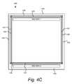
- FIGS. 4A-Bare cross section schematics depicting two side views of an electrochromic device.
- FIG. 4Cis a schematic top view of the electrochromic device described in relation to FIGS. 4A-B .
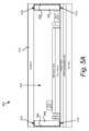
- FIG. 5Ais a cross section schematic showing the device described in relation to FIGS. 4A-C integrated into an IGU.
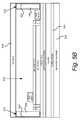
- FIG. 5Bis a cross section schematic showing the IGU as in FIG. 5A , where the EC pane is strengthened by lamination.
- electrochromic panesbe both strong and relatively free of defects.
- glass panesare strengthened by tempering.
- the tempering processcan introduce defects in an electrochromic device.
- most efforts to produce electrochromic windowsemploy a fabrication sequence of first cutting a glass pane to size, then tempering the glass, and finally forming the electrochromic device on the tempered window pane.
- the electrochromic deviceis typically formed by depositing a sequence of thin layers on one side of the pre-cut and tempered glass pane.
- the described sequence of cutting and then forming the EC devicefrequently gives rise to some low quality electrochromic windows because modern fabrication processes often produce one or more visible defects on an electrochromic device.
- the manufacturermay refuse to tolerate low quality devices, but rejection of low quality panes corresponds to a reduction in yield.
- an electrochromic deviceis fabricated to substantially cover a glass sheet. Only later is a cutting pattern for multiple electrochromic panes defined on the glass sheet.
- the cutting patternmay take into account various considerations including utilization of the sheet, defects in the EC device as fabricated, economic demand for particular sizes and shapes of EC panes, non-uniformity in the device and/or glass sheet, etc.
- problematic defectsoccur in only a very small or limited region or regions of the glass sheet. Once identified, these regions can be excluded when defining electrochromic panes in the cutting pattern. In this manner, the cutting pattern may account for high (or low) defectivity regions of the glass sheet. While it is often desirable to probe the EC device on the large glass sheet to identify and exclude regions of defects, it may sometimes be appropriate to exclude certain regions without probing the device. For example, it is sometimes observed that defects are concentrated around the perimeter of the large glass sheet. Therefore it is sometimes desirable to exclude the perimeter region from the pattern of electrochromic panes. In one example, between about 1 inches and about 10 inches around the perimeter of the glass sheet is removed after the electrochromic device is fabricated on the glass. In various embodiments, such perimeter regions are excluded as a matter of course, with the exact amount of excluded perimeter region being based on a knowledge of the quality control (QC) of a well-defined production fabrication process.
- QCquality control
- Scribes and/or bus bars for the individual panesare provided at some point after the cutting pattern is defined. As mentioned, these features may be provided to individual EC panes before and/or after the glass sheet is cut into one or more electrochromic panes according to the pattern. The cutting itself may employ a procedure that improves the strength of the resulting cut panes. Further, as explained below, the edges may be “finished” to mitigate problems created by cutting. Additionally, in some embodiments, IGUs are fabricated from the cut electrochromic panes and optionally one or more of the panes of the IGU are strengthened. More details of aspects of the invention are described below and with respect to the Figures.
- FIG. 1Adepicts a process flow, 100 , including a sequence of operations for manufacturing one or more electrochromic panes.
- First a glass sheetis received, see 110 .
- a large glass sheetis intended to be cut into smaller panes at a later stage of the process.
- the panesare intended to be used as windows, so the physical dimensions as well as the optical and mechanical properties of the substrate should be appropriate for the intended window application.
- the large glass sheet employed at operation 100is a piece of glass of between about 3 meters and about 6 meters in length on at least one side. In some cases, the glass is rectangular, being about 3 to 6 meters high and about 1.5 to 3 meters wide.
- the glass sheetis about 2 meters wide and about 3 meters high. In one embodiment, the glass is six feet by ten feet. Whatever the dimensions of the glass sheet, the EC pane fabrication equipment is designed to accommodate and process many such sheets, fabricating EC devices on such sheets, one after another in succession.
- Suitable glass for the glass sheetincludes float glass, Gorilla® Glass (a trade name for alkali-aluminosilicate sheet glass available from Dow Corning, Corp. of Midland, Mich.) and the like.
- Gorilla® Glassa trade name for alkali-aluminosilicate sheet glass available from Dow Corning, Corp. of Midland, Mich.
- EC devicescan be formed on other than glass substrates. Methods described herein are meant to include other substrates besides inorganic glass, for example, plexiglass would also work in some instances.
- glass sheetis used from herein to encompass all types of window substrate, unless otherwise specifically qualified.
- the glass sheetis float glass, optionally coated with a transparent conducting oxide (TCO) and a diffusion barrier layer.
- TCOtransparent conducting oxide
- examples of such glassesinclude conductive layer coated glasses sold under the trademark TEC® Glass by Pilkington, of Toledo, Ohio and SUNGATE® 300 and SUNGATE® 500 by PPG Industries of Pittsburgh, Pa.
- the glass sheethas a size that is at least equal to the largest EC glass pane contemplated for manufacture.
- TEC® Glassis a glass coated with a fluorinated tin oxide conductive layer. Such glass typically also has a diffusion barrier layer between the TCO and the float glass to prevent sodium from diffusing from the glass into the TCO.
- the glass sheetdoes not have a preformed TCO or diffusion barrier on it, for example, in one embodiment the diffusion barrier, a first TCO, an electrochromic stack and a second TCO are all formed in a single apparatus under a controlled ambient environment (infra).
- the glass sheetmay be heat strengthened prior to fabrication of an electrochromic (EC) device thereon.
- an electrochromic (EC) deviceis prepared on the glass sheet, see 120 .
- the EC deviceuses the TCO as one of its conductors.
- the glass sheetis float glass without any pre-formed coatings then typically 120 involves initially depositing a diffusion barrier layer, then a transparent conductor (typically a TCO) layer, and thereafter the remainder of the EC device is formed.
- another transparent conductor layer(typically a TCO layer) is deposited as a second conductor (to deliver power to the EC stack).
- TCO layertypically a TCO layer
- a hermetic layeris applied to keep moisture out of the device.
- a low-E (emissivity) coatingis applied.
- the electrochromic deviceis a low-defectivity all solid state and inorganic electrochromic device as described in the above applications.
- the EC deviceis manufactured on the glass sheet in apparatus having a controlled ambient environment, that is, an apparatus in which the layers are deposited without leaving the apparatus and without, for example, breaking vacuum between deposition steps, thereby reducing contaminants and ultimately device performance.
- This manufacturemay include deposition of a diffusion barrier on the glass sheet and the EC device including both electrodes (TCO layers).
- inspectionsmay be conducted internally at various points in the fabrication flow.
- one or more of the TCO, EC, IC, CE layersmay be inspected during processing.
- Optical, electrical, chemical, or mechanical inspectionsmay be employed to characterize one or more parameters of the layers.
- parametersinclude, for example, optical density, sheet resistance, thickness, defectivity, morphology, and the uniformity of any of these across the glass substrate surface.
- one or more inspectionsmay be performed after the entire EC device is fabricated on the glass sheet surface. As explained elsewhere herein, such inspection may characterize defectivity at regions on the surface and/or non-uniformities in the EC device.
- switchable optical devicesbesides electrochromic devices may be employed in the described process. Many such devices are formed as layers on an underlying substrate. Examples of suitable optical devices include various liquid crystal devices and electrophoretic devices including rotating element and suspended particle devices. Any of these can be fabricated or otherwise provided on a large glass sheet and then processed as described herein.
- a cutting patternis defined, see 130 .
- defining a cutting pattern after depositing the electrochromic deviceaffords considerable flexibility in determining which regions of the fabricated device are used and which are not used in the cut panes. It also, affords flexibility in determining appropriate sizes of the panes based on the overall quality of the fabricated electrochromic device. Of course, there are a range of considerations that drive the cutting pattern, and only some of them pertain to the quality or condition of the as fabricated device.
- the characteristics used in defining a pattern of EC panes on the glass sheetmay include any one or more of the following: (1) local defectivity or other measure of local quality (for example, a local non-uniformity in sheet resistance), (2) demand for particular grades of product (for example some end users specify a particular grade or quality of EC pane), (3) demand for particular sizes and shapes of products, (4) remake demand (caused by breakages and/or low yield fabrication of certain types of EC panes), (5) current inventory of EC device types on the glass sheets and/or individual EC panes, (6) utilization of the area of the overall glass sheet, and (7) global properties of the EC device (for example, EC device leakage current and electrode (TCO) resistance).
- local defectivity or other measure of local qualityfor example, a local non-uniformity in sheet resistance
- demand for particular grades of productfor example some end users specify a particular grade or quality of EC pane
- demand for particular sizes and shapes of productsfor particular sizes and shapes of products
- remake demandca
- a global propertymight dictate the appropriate size or grade of the final EC pane(s). For example, high EC device leakage current or high TCO resistance might indicate that the resulting EC panes must be relatively small (for example, not greater than about 20 inches). Stated another way, the glass sheets, each with a fabricated EC device thereon, are binned based on global properties.
- one or more of the panes defined in the patternare sized and shaped for residential window applications. In some cases, one or more of the panes defined in the pattern are sized and shaped for commercial window applications.
- defining a cutting pattern for cutting the glass sheet in order to create the one or more electrochromic panescan include characterizing one or more physical features of the glass sheet and/or electrochromic device after fabrication of the electrochromic device.
- characterizing the one or more physical featuresinclude at least one of: 1) identifying one or more low-defectivity areas on the electrochromic device, 2) identifying one or more areas of non-uniformity in the electrochromic device, 3) identifying one or more areas where materials used to make the electrochromic device were deposited on the back side of the glass sheet; 4) identifying one or more performance characteristics of the electrochromic device; and 5) identifying one or more defects in the glass sheet.
- Non-uniform areas in the EC deviceare, for example, areas where, for example, the coloration is not uniform due to variation in thickness of layers of the EC device, variation in properties of the device, for example, due to uneven heating during formation of the EC stack, and the like. Non-uniform areas thus may be independent of the number of, for example, short related optical defects. It may be desirable to remove these areas from the cutting pattern or include them in the cutting pattern but identify them as, for example, being areas from which a different quality of EC pane will be cut.
- materials used to make the electrochromic devicecan be deposited on the back side of the glass sheet due to overspray. This is undesirable and therefore the presence of backside deposition is a useful characteristic of the glass sheet after EC device formation. Areas with backside materials may be cleaned to remove the unwanted material and/or these areas are excluded from the cutting pattern. Performance characteristics of the electrochromic device are also an important parameter for characterizing the EC device. As described above, for example, an EC device may be used in different ways depending on whether it falls into a certain specification category.
- Identifying one or more defects in the glass sheetis also important, for example, irrespective of the EC device's performance, there may be a defect in the glass sheet, like a bubble or fissure trapped in the glass, that would be excluded from the cutting pattern due to its undesirable optical properties.
- the cutting patternis defined (operation 130 of FIG. 1A ) by first detecting and mapping the defectivity of the device across the glass sheet and then excluding or relegating areas of high defectivity from one or more electrochromic panes in the cutting pattern.
- FIG. 1Bprovides an example process flow for this embodiment.
- the glass sheet's deviceis scribed in order to define a usable area, which is typically substantially the entire area of the device as prepared on the glass sheet.
- the scribingmay serve two purposes. First it electrically isolates the two electrodes to provide a functioning device, and second it removes clearly defective portions of the EC stack.
- edge regions of the glass sheetexhibit roll off and/or other imperfections, and thus present the very real issue of short circuits.
- the edge regions of the deviceare isolated or removed. Techniques for accomplishing this include scribing (presented in FIG. 1B ), edge deleting, or simply removing the glass sheet and associated device over some fraction of the perimeter.
- the deviceis activated by application of electrical energy to color or otherwise change the optical properties of the device so that the device can be characterized and any defects can be detected, see 133 .
- deviceis characterized including identifying any defects and optionally classifying the defects as to type and/or severity, see 134 .
- non-uniformities in the EC deviceare characterized at this stage as well. and taken into account when defining the cutting pattern.
- this characterizationincludes the glass pane as well as the EC device on the glass pane.
- the identification and/or classificationis performed by the naked eye. In other examples, this operation is performed by an automated scanning device.
- larger short-type visual defectsare mitigated by application of electrical or optical energy.
- such defectsare circumscribed by laser ablation to create smaller pin-hole type defects. These mitigated defects may be included in the defect count when identifying regions of low defectivity.
- this ablation or other mitigationis performed after the panes are cut from the glass sheet.
- activating the EC device and scrutinizing the deviceis only one way to detect and identify defects.
- Other methodsinclude using diffraction, reflection, or refraction of various forms of electromagnetic radiation that interact with the EC device, for example, polarized light and/or lock-in infrared (IR) thermography.
- Lock-in IR thermographyis a non-destructive and non-contacting technique for the spatially resolved detection of small leakage currents in electronic materials that involves applying a temperature source to the material (in this case the EC device) and detecting leakage current induced temperature variations with, for example, an infrared camera.
- embodimentsinclude not only activating the EC device to identify defects, but also may include, or use in the alternative, other methods of identifying defectivity.
- the cutting pattern defined on the glass sheetmay exclude one or more high-defectivity areas of the electrochromic device provided on the glass sheet.
- the fabrication sequences contemplated hereinfrequently involve identifying regions of low or high defectivity prior defining a cutting pattern.
- “low-defectivity” areasare regions of the electrochromic device with fewer than a threshold number or density of defects. Defects may be identified and characterized in various ways. In certain embodiments, defects are identified and/or classified as described in U.S. patents application Ser. Nos. 12/645,111 and 12/645,159, both previously incorporated by reference.
- Visual defectsinclude short-type defects that produce a halo when the device is darkened.
- a halois a region in the device where an electrical short across the electrochromic stack causes an area around the short to drain current into the short and therefore the area surrounding the short is not darkened.
- These short defectsare conventionally treated after fabrication of the electrochromic device, for example laser circumscribed to isolate them and remove the halo effect, which leaves smaller short-related pinhole defects.
- defects visible to the naked eyeare on the order of 100 ⁇ m in diameter.
- the total number of visible defects, pinholes and short-related pinholes created from isolating visible short-related defects, in a low-defectivity areais less than about 0.1 defects per square centimeter, in another embodiment less than about 0.08 defects per square centimeter, in another embodiment less than about 0.045 defects per square centimeter (less than about 450 defects per square meter of electrochromic pane). Smaller defects, for example defects not visible to the naked eye (on the order of 40 ⁇ m or less), may be tolerable in higher densities in some embodiments.
- the defects that are detected and optionally classified in the glass sheetare mapped, see operation 135 of FIG. 1B . This can be done, for example, by marking the glass to show where the defects are located once the device is inactive, and/or by storing the defect pattern in a memory as a map. This mapping information is analyzed to identify one or more low-defectivity regions from which to cut the one or more EC panes, see 136 .
- One embodiment of the depicted methoddefines the cutting pattern by (a) creating a first mapping data set based on the one or more low-defectivity areas on the electrochromic device; (b) creating a second mapping data set based on another one or more low-defectivity areas on a second electrochromic device on a second glass sheet; (c) comparing the first and second mapping data sets; and (d) defining the cutting pattern using the comparison of the first and second mapping data sets to maximize efficient use of the glass sheet.
- the mappingmay be used to match two compatible EC sheets for use in a single IGU so that defects in the respective panes do not align.
- mapping data setsare stored in a memory and (c) and (d) are performed using an appropriate algorithm or other logic.
- these mapping data sets and comparisons thereofdefine the most efficient use of the glass sheet's device.
- mapping data for two glass sheetsmay indicate that the most efficient use of the glass would be to cut the two sheets to accommodate different customers' specifications due to defectivity patterns that, if not present, would otherwise dictate cutting the sheets according to a single customer's specifications.
- the logicmay define panes of varying sizes from each glass sheet in order to supply electrochromic panes for a variety of window types and end users, for example, by pane size, defectivity level and the like. Once the one or more low-defectivity regions are used to define the cutting pattern and process flow 130 ends.
- FIG. 2Adepicts a glass sheet, 200 , for example about 3 meters by about 2 meters, or about 120 inches by 72 inches, with an EC device (not shown separately) thereon.
- a cutting pattern(as indicated by the dotted lines) is defined for cutting one or more electrochromic panes from glass sheet 200 .
- the cutting patterncan be regular, such as pattern 202 , or irregular, such as pattern 204 .
- Pattern 204shows, for example, areas 206 a and 206 b , which collectively make a strip of glass that is to be discarded due to, for example, roll off and/or higher defect levels than the rest of the glass sheet. These perimeter areas may also be removed because of back side contamination of EC device materials due to overspray.
- the one or more EC panescan be of the same size, or varying size depending on the need.
- edges of the sheetmay be removed prior to cutting the glass sheet. In some embodiments about 1 to 10 inches of glass are removed around some or all of the glass sheet's perimeter. This edge trimming can be done for a variety of reasons. For example, the quality of the EC device may be inferior around the perimeter of the glass sheet. This low quality around the perimeter may be due to rolloff of the EC device stack, imperfections in the edge of the glass sheet (which can interfere with the EC device fabrication), propagation of such edge defects (e.g. fissures), and cathode dimensions as they relate to the glass sheet dimensions during deposition. Also, deposition of materials on the back side of the glass sheet due to overspray may necessitate trimming the edges of the glass.
- Non-uniformities in the EC devicemay occur due to contact of the support pallet during processing of the EC device or non-uniform heating near the edges of the glass. Some of these defects can be appreciated without powering the EC device and therefore edge trimming may be performed prior to testing the device. Thus edge trimming may be performed as a matter of course or as a result of, for example, performing test runs of the EC formation and finding that the process parameters require that edge trimming be performed post device fabrication to remove non-uniformities and/or back side overspray.
- scribesare performed according to the needs of each individual EC pane to be cut from the glass sheet, see 140 .
- a more detailed description of scribes used to fabricate individual EC panesis described below in relation to FIGS. 3A-C .
- the scribesare made prior to the individual EC panes being cut from the glass sheet. This saves time and resources that would otherwise be needed in order to scribe the individual panes, since a wide variety of pane sizes are contemplated as arising from the single glass sheet.
- the scribesare made after the glass sheet is cut into individual EC panes (infra).
- the EC devices on the glass sheetafter the EC devices on the glass sheet have been scribed, they are cut from the glass sheet according to the cutting pattern, see 150 .
- the cuttingcan be accomplished by any suitable process. In some cases, the cutting is accompanied by an edge finishing operation.
- Mechanical cuttingtypically involves scoring the glass with a hard tool, such as a diamond tip on a wheel, followed by snapping the glass along the score line. Thus, mechanical cutting includes “scoring” and breaking. Sometimes the term “scoring” is referred to as “scribing” in the glass window fabrication industry. However, to avoid confusion with other operations described herein, use of “scribe” will be reserved for these other operations.
- Cuttingcan produce microcracks and internal stresses proximate the cut. These can result in chipping or breaking of the glass, particularly near the edges.
- cut glassmay be subject to edge finishing, for example, by mechanical and/or laser methods.
- Mechanical edge finishingtypically involves grinding with, for example, a grinding wheel containing clay, stone, diamond, etc.
- the resulting edge surfaceis relatively rounded and crack free.
- Laser edge finishingtypically produces a flat, substantially defect free surface. For example, an initial cut through the glass, perpendicular to the surface of the glass, may make a substantially defect free cut. However the right angle edges at the perimeter of the glass are susceptible to breakage due to handling.
- a laseris used subsequently to cut off these 90 degree edges to produce a slightly more rounded or polygonal edge.
- cutting and optional edge finishing processesinclude the following: (1) mechanical cutting, (2) mechanical cutting and mechanical edge finishing, (3) laser cutting, (4) laser cutting and mechanical edge finishing, and (5) laser cutting and laser edge finishing.
- the panesare cut from the glass sheet in a manner that actually strengthens and/or improves the edge quality of the resulting panes.
- thisis accomplished using laser induced scoring by tension.
- a gas laserfor example a CO 2 laser with a wavelength of 10.6 ⁇ m
- a cooling devicefor example a gas and/or water jet, is used to quickly cool the heated line. This causes a score to form in the glass along the cutting line. The glass is then snapped by, for example, a conventional mechanical breaking device along the score.
- the cut linesare extremely clean, that is, there are minimal if any defects in the glass that can propagate and cause further breakage due to stresses applied to the pane.
- the edgesare subsequently mechanically and/or laser finished to remove the 90 degree edges to create a more rounded and/or polygonal edge.
- edge deletionis carried out on the individual EC panes, see 160 .
- Edge deletionis part of a manufacturing process for integrating the electrochromic device into, for example an IGU, where edge portions of the EC device, for example roll off (where layers of the device can make contact due to non-uniformity near the edge of for example a mask) and/or where a cut is made, are removed prior to integration of the device into the IGU or window. Where unmasked glass is used, removal of the coating that would otherwise extend to underneath the IGU frame (which is undesirable for long term reliability) is removed prior to integration into the IGU.
- Edge deletionis also used when a pane is cut from the glass sheet, as the panes will have EC material running to the edges of the pane.
- isolation trenchesare cut and the isolated portions of the EC device on the perimeter of the panes is removed by edge deletion.
- Edge deletioncan be performed at any stage post formation of the EC device in the process flows described.
- the process of performing edge deletionis, in some embodiments, a mechanical process such as a grinding or sandblasting process. An abrasive wheel may be employed in for grinding.
- edge deletionis done by laser, for example, where a laser is used to ablate EC material from the perimeter of the pane.
- the processmay remove all EC layers including the underlying TCO layer or it may remove all EC layers except this bottom TCO layer.
- the later caseis appropriate when the edge delete is used to provide an exposed contact for a bus bar, which must be connected to the bottom TCO layer.
- a laser scribeis used to isolate that portion of the bottom TCO that extends to the edge of the glass from that which is connected to the bus bar in order to avoid having a conductive path to the device from the edge of the glass.
- edge deletionWhen edge deletion is to be used, it can be done before or after the EC panes are cut from the glass sheet. In certain embodiments, edge deletion may be carried out in some edge areas prior to cutting the EC panes, and again after they are cut. In certain embodiments, all edge deletion is performed prior to cutting the panes. In embodiments employing “edge deletion” prior to cutting the panes, portions of the EC device on the glass sheet can be removed in anticipation of where the cuts (and thus edges) of the newly formed EC panes will be. In other words, there is no actual edge yet, only a defined area where a cut will be made to produce an edge. Thus “edge deletion” is meant to include removing EC device material in areas where an edge is anticipated to exist.
- bus barsare applied to the one or more EC panes, see 170 .
- edge deletionthe addition of bus bars can be performed after the EC panes are cut from the glass sheet or before, but after scribing.
- the scribe, edge deletion and bus bar applicationprior to cutting the panes from the glass sheet, the associated special handling steps for a variety of EC pane sizes are avoided. That is, performing various manipulations and/or component integrations before the individual panes are cut from the glass sheet allows use of apparatus for handling the glass sheets of uniform size for maximum efficiency.
- the glass sheetis cut according to 150 , then edge deletion is performed according to 160 , and thereafter the EC devices are scribed according to 140 .
- edge deletionis performed at the edges of the individual EC panes, and then the scribes are applied.
- the glass sheetis cut according to 150 , then the EC devices are scribed according to 140 , and then edge deletion is performed according to 160 .
- One advantage of scribing and deleting post cuttingis uniformity in the edge deletion process, since only material from the perimeter where actual cut edges (rather than from areas where an edge is anticipated to exist post cutting) is removed. This method may include higher quality control since the edge of the glass can be used as a guide for the edge deletion.
- an IGUis formed by placing sealing separator, for example, a gasket or seal (for example made of PVB (polyvinyl butyral), PIB or other suitable elastomer) around the perimeter of the glass sheet.
- the sealing separatorincludes a metal, or other rigid material, spacer and sealant between the spacer and each glass pane.
- a secondary sealis provided around the outer perimeter of the spacer, for example a polymeric material that resists water and that adds structural support to the assembly.
- a desiccantis included in the IGU frame or spacer during assembly to absorb any moisture.
- the sealing separatorsurrounds the bus bars and electrical leads to the bus bars extend through the seal.
- the IGUis filled with inert gas such as argon.
- the completed IGUcan be installed in, for example, a frame or curtain wall and connected to a source of electricity and a controller to operate the electrochromic window.
- glass sheet 200is cut according to a cutting pattern derived, for example, as described herein.
- four (EC) panes, 208are produced.
- two of panes 208are paired and combined with a sealing separator, 210 , to form an IGU, 212 .
- IGU 212has two EC panes.
- the panesare arranged so that EC devices face inside the IGU so as to be protected from the ambient.
- Electrochromic windows having two or more electrochromic panesare described in U.S.
- Multipane Electrochromic Windowswhich is incorporated by reference herein for all purposes. Methods described therein are particularly useful for making one or more electrochromic panes for use in multipane electrochromic windows.
- One advantage to such multipane electrochromic windowsis that the likelihood of two defects aligning perfectly, and thus being observable to the end user, is quite small. This advantage is accentuated when low-defectivity panes are used.
- the aforementioned (defect) mapping data setscan be used to further ensure that defects on individual panes, when registered in an IGU, do not align. This is yet another criterion that may be considered in patterning the glass sheet.
- the glass sheetis up to 5 mm or even up to 6 mm thick (up to 1 ⁇ 4 inch).
- one or more panesare strengthened.
- one or both panes of the IGUare strengthened, see 190 .
- strengtheningincludes laminating one or more of the panes of the IGU with, for example, a thicker pane of float glass, a pane of tempered glass, a polymeric pane such as plexiglass, Gorilla® Glass, and the like.
- strengtheningincludes applying a polymeric coating to one or more panes of the IGU.
- polymeric coatingsexamples include ormosil polymeric coatings (epoxy resin, an amine hardener and a silane), sol-gel coatings, acrylic glazes, and other safety glazes, for example commercially available glazes which meet one or more impact test standards.
- ormosil polymeric coatingsepoxy resin, an amine hardener and a silane
- sol-gel coatingsacrylic glazes
- acrylic glazesfor example commercially available glazes which meet one or more impact test standards.
- an edge bumperis employed to protect the edges of the glass after incorporation in the IGU. The protection allows the IGU to be safely transported from manufacturer to installation, for example.
- a protective edge bumpermay be applied to IGUs with or without strengthened panes.
- the protective bumperis a U-channel cap which fits over the glass edges around the perimeter of the IGU. It may be made from an elastomeric or plastic material. In one example, it is a vinyl cap.
- Laminating an EC pane with a reinforcing substrate (or pane) after incorporation into an IGUhas many benefits.
- lamination after the EC pane is assembled in an IGUprotects the EC device during the lamination process and provides ease of handing. This is particularly true if the EC device is on an inner facing surface of the IGU, that is, in the interior insulating region of the IGU, because lamination processes involve contacting the outer surfaces of the glass panes making up the lamination structure under relatively harsh conditions. Under such conditions, the EC device would be damaged if it was located on the outer surface of a lamination structure. The IGU thus protects the device during lamination.
- the lamination panewould require lamination directly onto the EC device with the reinforcing pane and/or the adhesive used to attach it (the lamination pane). While lamination can be conducted without damaging the EC device, this approach has some downsides. Most notably, the IGU would be a less effective thermal insulator because radiation is blocked only at the interior of the IGU. Further, the exposed edges of the EC device, located around the perimeter of the IGU, may provide an ingress point for moisture after installation.
- liquid resin laminationis used to strengthen an EC pane after it is incorporated into an IGU.
- FIG. 3Aschematically depicts aspects of a process flow for liquid resin lamination of an IGU, 300 .
- IGU 300is drawn in less detail than for example IGU 212 described in relation to FIG. 2B .
- IGU 300has an EC pane and a non-EC pane.
- double sided tape, 305is applied to a perimeter region of the EC pane.
- a gap, 315is left in the perimeter tape, for example, in a corner of the pane.
- a reinforcing pane, 310is applied to the double-sided tape, so that a triple pane (see also FIG.
- the reinforcing paneis laminated to the EC pane of the IGU, and there is also the non-EC pane of the IGU which is not part of the laminate) structure, 320 , is formed.
- a liquid resin, 325is introduced, for example from the bottom as depicted, in the volume formed between the EC pane and reinforcing pane 310 . This can be accomplished, for example, by leaving a small portion of the backing of the tape on when pane 310 is applied to the tape and registered with the EC pane.
- a dispensing nozzlein the shape of a thin blade, is inserted in between pane 310 and the portion of the tape with the backing remaining.
- the resinis introduced into the volume and the blade removed, the remaining tape backing is removed so that the only means of exit for the resin is gap 315 .
- unit 320is then rotated so that the liquid resin 325 flows toward gap 315 (as indicated in the lower left diagram by the heavy dotted arrow downward).
- the appropriate amount of resinis introduced into the volume so that when the resin covers the entire area between the panes and within the tape, the panes are substantially parallel to each other.
- the resinis cured, for example, via heating, a catalyst and/or exposure to UV irradiation to form a strong bond between the panes.
- the cured resinhas the desired optical, mechanical and other properties of the lamination. Using liquid resin lamination imparts minimal if any stress on the EC pane during lamination.
- FIG. 3Bis a cross section showing more detail of the final assembly 320 .
- the IGU portion, 300includes a first pane, 301 , and an EC pane, 302 , which includes an EC device, 303 , thereon.
- Panes 301 and 302are separated by a sealing separator, 304 , which spans the perimeter of the panes and has seals between it and each pane.
- An interior space, 330is defined by the panes and the sealing separator.
- Tape 305lies between (and proximate to the perimeter) of the face of the EC pane outside of the IGU's interior space and pane 310 .
- the cured resin, 325Inside the volume created between the EC pane and pane 310 is the cured resin, 325 .
- the resinmay contain additives that impart a desired optical property to the resulting laminate.
- optical propertiesinclude color, opacity, scattering and reflectivity.
- the resinimparts a blue color. This can be particularly beneficial when used with some EC devices that have a naturally yellowish tint.
- the optical propertycan be imparted by adding dyes, pigments, scattering particles, metallic dust, etc. to the liquid resin prior to introduction into volume for lamination.
- the blue coloris achieved as a result of a chemical reaction that takes place after the resin is introduced into the volume between the panes.
- the reactionmay be catalyzed by the same energy or reagent that catalyzes the curing of the resin.
- the resinchanges to a blue color after curing, for example, by exposure to normal ambient lighting and/or specific irradiation and/or heating post cure.
- FIG. 4Ais a cross-sectional representation of an electrochromic pane, 400 , which is fabricated starting with a glass sheet, 405 , for example as outlined in process flow 100 .
- FIG. 4Bshows the cross sectional view from another side of EC pane 400
- FIG. 4Cshows a top view of EC pane 400 ( FIG. 4A is the view from the right or left side as depicted in FIG. 4C ; and FIG. 4B is the view from the bottom side looking up as depicted in FIG. 4C ).
- FIG. 4Ais the view from the right or left side as depicted in FIG. 4C
- FIG. 4Bis the view from the bottom side looking up as depicted in FIG. 4C ).
- FIG. 4Ais the view from the right or left side as depicted in FIG. 4C
- FIG. 4Bis the view from the bottom side looking up as depicted in FIG. 4C ).
- FIG. 4Ais the view from the right or left side as depict
- the glass pane, 405has a diffusion barrier, 410 , and a first transparent conducting oxide (TCO) 415 on the diffusion barrier.
- the TCO layer 415is the first of two conductive layers used to form the electrodes of the electrochromic device fabricated on the glass sheet.
- the glass sheetincludes underlying glass and the diffusion barrier layer.
- the diffusion barrieris formed, then the first TCO, then the EC stack, and then the second TCO.
- the electrochromic device(EC stack and second TCO) is fabricated in an integrated deposition system where the glass sheet does not leave the integrated deposition system at any time during fabrication of the stack.
- the first TCO layeris also formed using the integrated deposition system where the glass sheet does not leave the integrated deposition system during deposition of the EC stack and the (second) TCO layer.
- all of the layersare deposited in the integrated deposition system where the glass sheet does not leave the integrated deposition system during deposition.
- FIG. 4Adepicts areas 440 where the device has been removed, in this example, from a perimeter region surrounding the laser scribe trenches, 430 , 431 , 432 and 433 , which pass through the second TCO and the EC stack, but not the first TCO, are made to isolate portions of the EC device, 435 , 436 , 437 and 438 , that were potentially damaged during edge deletion from the operable EC device.
- laser scribes 430 , 432 , and 433pass through the first TCO to aide in isolation of the device (laser scribe 431 does not pass through the first TCO, otherwise it would cut off bus bar 2 's electrical communication with the first TCO and thus the EC stack).
- the laser or lasers used for the laser scribesare typically, but not necessarily, pulse-type lasers, for example diode-pumped solid state lasers.
- the laser scribescan be performed using a suitable laser from IPG Photonics (of Oxford Mass.), or from Ekspla (of Vilnius Lithuania). Scribing can also be performed mechanically, for example, by a diamond tipped scribe.
- the laser scribescan be performed at different depths and/or performed in a single process whereby the laser cutting depth is varied, or not, during a continuous path around the perimeter of the EC device.
- the edge deletionis performed to the depth below the first TCO.
- a second laser scribeis performed to isolate a portion of the first TCO, for example as depicted in FIGS. 4A-C , near the edge of the glass pane from that toward the interior. In one example this scribe is at least along the edge where bus bar 2 is applied to the first TCO, between bus bar 2 and the edge.
- Non-penetrating bus bar ( 1 )is applied to the second TCO.
- Non-penetrating bus bar ( 2 )is applied to an area where the device was not deposited (for example from a mask protecting the first TCO from device deposition), in contact with the first TCO or in this example, where edge deletion was used to remove material down to the first TCO.
- both bus bar 1 and bus bar 2are non-penetrating bus bars.
- a penetrating bus baris one that is typically pressed into and through the EC stack to make contact with the TCO at the bottom of the stack.
- a non-penetrating bus baris one that does not penetrate into the EC stack layers, but rather makes electrical and physical contact on the surface of a conductive layer, for example, a TCO.
- the TCO layer'scan be electrically connected using a non-traditional bus bar, for example, screen and lithography patterning methods.
- electrical communicationis established with the device's transparent conducting layers via silk screening (or using another patterning method) a conductive ink followed by heat curing or sintering the ink.
- Advantages to using the above described device configurationinclude simpler manufacturing, for example, less laser scribing than conventional techniques which use penetrating bus bars, and the fact that the EC device colors to, and under, bus bar 1 (unlike conventional methods which cut an isolation trench through the device when bus bar 1 is a penetrating type bus bar), which provides a larger coloration area.
- Penetrating bus bar'scan be used, for example in place of non-penetrating bus bar 1 , but this will sacrifice colorable area and would necessitate a scribe through the first TCO, prior to fabrication of the EC stack on the glass.
- One embodimentcontemplates performing this first scribe for the one or more EC devices on the glass sheet prior to fabrication of the EC device thereon. In such embodiments, the remainder of the method flow, for example as described in relation to FIGS. 1A and 1B , remains analogous.
- FIG. 5Adepicts a cross section of the EC pane as described in relation to FIGS. 4A-C integrated into an IGU, 500 .
- a spacer, 505is used to separate EC pane 400 from another pane, 510 .
- the second pane 510 in this exampleis a non-EC pane, however the invention is not so limited.
- Pane 510can have an EC device thereon and/or one or more coatings such as low-E coatings and the like. Between spacer 505 and, in this example, the first TCO of EC device 400 , is a primary seal, 515 . This seal is also between separator 505 and the second glass pane. Around the perimeter of separator 505 is a secondary seal, 520 (bus bar wiring traverses the seal for connection to controller). These seals aid in keeping moisture out of the interior space, 515 , of the IGU.
- FIG. 5Bdepicts IGU 500 after lamination with a reinforcing pane, 530 .
- a liquid resin laminationwas used, and thus, cured resin, 535 , lies between the reinforcing pane and the glass of the EC pane.
- cured resin, 535lies between the reinforcing pane and the glass of the EC pane.
- glass 2also had an EC device thereon, it could also be laminated.
- One embodimentis an IGU including two EC panes separated by an interior space, in one example both EC devices are in the interior space of the IGU, where both EC panes are reinforced.
- the EC panesare reinforced with liquid resin lamination as described herein.
- one or both of the EC panesare reinforced or strengthened by applying a coating as described herein.
Landscapes
- Physics & Mathematics (AREA)
- Nonlinear Science (AREA)
- Optics & Photonics (AREA)
- General Physics & Mathematics (AREA)
- Structural Engineering (AREA)
- Engineering & Computer Science (AREA)
- Chemical & Material Sciences (AREA)
- Crystallography & Structural Chemistry (AREA)
- Mathematical Physics (AREA)
- Architecture (AREA)
- Civil Engineering (AREA)
- Electrochromic Elements, Electrophoresis, Or Variable Reflection Or Absorption Elements (AREA)
- Inorganic Chemistry (AREA)
Abstract
Description
Claims (21)
Priority Applications (14)
| Application Number | Priority Date | Filing Date | Title |
|---|---|---|---|
| US13/431,729US9102124B2 (en) | 2010-11-08 | 2012-03-27 | Electrochromic window fabrication methods |
| US13/456,056US9958750B2 (en) | 2010-11-08 | 2012-04-25 | Electrochromic window fabrication methods |
| US14/512,297US9703167B2 (en) | 2010-11-08 | 2014-10-10 | Electrochromic window fabrication methods |
| US14/740,114US9513525B2 (en) | 2010-11-08 | 2015-06-15 | Electrochromic window fabrication methods |
| US15/226,835US10241375B2 (en) | 2010-11-08 | 2016-08-02 | Electrochromic window fabrication methods |
| US15/364,162US9995985B2 (en) | 2010-11-08 | 2016-11-29 | Electrochromic window fabrication methods |
| US15/934,854US10409130B2 (en) | 2010-11-08 | 2018-03-23 | Electrochromic window fabrication methods |
| US16/267,260US10684524B2 (en) | 2010-11-08 | 2019-02-04 | Electrochromic window fabrication methods |
| US16/523,852US11065845B2 (en) | 2010-11-08 | 2019-07-26 | Electrochromic window fabrication methods |
| US17/309,332US20220137472A9 (en) | 2010-11-08 | 2019-11-26 | Adhesive bus bars in electrochromic windows |
| US16/863,945US11772366B2 (en) | 2010-11-08 | 2020-04-30 | Electrochromic window fabrication methods |
| US17/304,012US20220032584A1 (en) | 2010-11-08 | 2021-06-11 | Electrochromic window fabrication methods |
| US18/459,355US12233625B2 (en) | 2010-11-08 | 2023-08-31 | Electrochromic window fabrication methods |
| US19/017,123US20250144919A1 (en) | 2010-11-08 | 2025-01-10 | Electrochromic window fabrication methods |
Applications Claiming Priority (2)
| Application Number | Priority Date | Filing Date | Title |
|---|---|---|---|
| US12/941,882US8164818B2 (en) | 2010-11-08 | 2010-11-08 | Electrochromic window fabrication methods |
| US13/431,729US9102124B2 (en) | 2010-11-08 | 2012-03-27 | Electrochromic window fabrication methods |
Related Parent Applications (3)
| Application Number | Title | Priority Date | Filing Date |
|---|---|---|---|
| US12/941,882ContinuationUS8164818B2 (en) | 2010-11-08 | 2010-11-08 | Electrochromic window fabrication methods |
| US13/312,057Continuation-In-PartUS8711465B2 (en) | 2010-11-08 | 2011-12-06 | Spacers for insulated glass units |
| US13/456,056ContinuationUS9958750B2 (en) | 2010-11-08 | 2012-04-25 | Electrochromic window fabrication methods |
Related Child Applications (3)
| Application Number | Title | Priority Date | Filing Date |
|---|---|---|---|
| US13/456,056Continuation-In-PartUS9958750B2 (en) | 2010-11-08 | 2012-04-25 | Electrochromic window fabrication methods |
| US13/456,056ContinuationUS9958750B2 (en) | 2010-11-08 | 2012-04-25 | Electrochromic window fabrication methods |
| US14/740,114ContinuationUS9513525B2 (en) | 2010-11-08 | 2015-06-15 | Electrochromic window fabrication methods |
Publications (2)
| Publication Number | Publication Date |
|---|---|
| US20120182593A1 US20120182593A1 (en) | 2012-07-19 |
| US9102124B2true US9102124B2 (en) | 2015-08-11 |
Family
ID=45526468
Family Applications (8)
| Application Number | Title | Priority Date | Filing Date |
|---|---|---|---|
| US12/941,882Active2030-12-04US8164818B2 (en) | 2010-11-08 | 2010-11-08 | Electrochromic window fabrication methods |
| US13/431,729ActiveUS9102124B2 (en) | 2010-11-08 | 2012-03-27 | Electrochromic window fabrication methods |
| US14/740,114ActiveUS9513525B2 (en) | 2010-11-08 | 2015-06-15 | Electrochromic window fabrication methods |
| US15/226,835ActiveUS10241375B2 (en) | 2010-11-08 | 2016-08-02 | Electrochromic window fabrication methods |
| US16/267,260ActiveUS10684524B2 (en) | 2010-11-08 | 2019-02-04 | Electrochromic window fabrication methods |
| US16/863,945ActiveUS11772366B2 (en) | 2010-11-08 | 2020-04-30 | Electrochromic window fabrication methods |
| US18/459,355ActiveUS12233625B2 (en) | 2010-11-08 | 2023-08-31 | Electrochromic window fabrication methods |
| US19/017,123PendingUS20250144919A1 (en) | 2010-11-08 | 2025-01-10 | Electrochromic window fabrication methods |
Family Applications Before (1)
| Application Number | Title | Priority Date | Filing Date |
|---|---|---|---|
| US12/941,882Active2030-12-04US8164818B2 (en) | 2010-11-08 | 2010-11-08 | Electrochromic window fabrication methods |
Family Applications After (6)
| Application Number | Title | Priority Date | Filing Date |
|---|---|---|---|
| US14/740,114ActiveUS9513525B2 (en) | 2010-11-08 | 2015-06-15 | Electrochromic window fabrication methods |
| US15/226,835ActiveUS10241375B2 (en) | 2010-11-08 | 2016-08-02 | Electrochromic window fabrication methods |
| US16/267,260ActiveUS10684524B2 (en) | 2010-11-08 | 2019-02-04 | Electrochromic window fabrication methods |
| US16/863,945ActiveUS11772366B2 (en) | 2010-11-08 | 2020-04-30 | Electrochromic window fabrication methods |
| US18/459,355ActiveUS12233625B2 (en) | 2010-11-08 | 2023-08-31 | Electrochromic window fabrication methods |
| US19/017,123PendingUS20250144919A1 (en) | 2010-11-08 | 2025-01-10 | Electrochromic window fabrication methods |
Country Status (5)
| Country | Link |
|---|---|
| US (8) | US8164818B2 (en) |
| EP (2) | EP3876030A1 (en) |
| CN (2) | CN110187583A (en) |
| TW (7) | TWI528096B (en) |
| WO (1) | WO2012064510A1 (en) |
Cited By (25)
| Publication number | Priority date | Publication date | Assignee | Title |
|---|---|---|---|---|
| US9513525B2 (en) | 2010-11-08 | 2016-12-06 | View, Inc. | Electrochromic window fabrication methods |
| US10295880B2 (en) | 2011-12-12 | 2019-05-21 | View, Inc. | Narrow pre-deposition laser deletion |
| US10551711B2 (en) | 2009-03-31 | 2020-02-04 | View, Inc. | Fabrication of low defectivity electrochromic devices |
| US10606142B2 (en) | 2011-12-12 | 2020-03-31 | View, Inc. | Thin-film devices and fabrication |
| US10705363B2 (en) | 2017-07-13 | 2020-07-07 | Cardinal Ig Company | Electrical connection configurations for privacy glazing structures |
| US10739658B2 (en) | 2011-12-12 | 2020-08-11 | View, Inc. | Electrochromic laminates |
| US10795232B2 (en) | 2011-12-12 | 2020-10-06 | View, Inc. | Thin-film devices and fabrication |
| US10802371B2 (en) | 2011-12-12 | 2020-10-13 | View, Inc. | Thin-film devices and fabrication |
| US10866480B2 (en) | 2017-04-20 | 2020-12-15 | Cardinal Ig Company | High performance privacy glazing structures |
| US10968684B2 (en) | 2018-08-17 | 2021-04-06 | Cardinal Ig Company | Privacy glazing structure with asymetrical pane offsets for electrical connection configurations |
| US11048137B2 (en) | 2011-12-12 | 2021-06-29 | View, Inc. | Thin-film devices and fabrication |
| US11065845B2 (en) | 2010-11-08 | 2021-07-20 | View, Inc. | Electrochromic window fabrication methods |
| US11111720B2 (en) | 2019-02-08 | 2021-09-07 | Cardinal Ig Company | Low power driver for privacy glazing |
| US11175523B2 (en) | 2019-04-29 | 2021-11-16 | Cardinal Ig Company | Staggered driving electrical control of a plurality of electrically controllable privacy glazing structures |
| US11243421B2 (en) | 2018-05-09 | 2022-02-08 | Cardinal Ig Company | Electrically controllable privacy glazing with energy recapturing driver |
| US11325352B2 (en) | 2019-04-29 | 2022-05-10 | Cardinal Ig Company | Leakage current detection and control for one or more electrically controllable privacy glazing structures |
| US11360364B2 (en) | 2017-11-06 | 2022-06-14 | Cardinal Ig Company | Privacy glazing system with discrete electrical driver |
| US11426979B2 (en) | 2011-12-12 | 2022-08-30 | View, Inc. | Thin-film devices and fabrication |
| US11448910B2 (en) | 2019-04-29 | 2022-09-20 | Cardinal Ig Company | Systems and methods for operating one or more electrically controllable privacy glazing structures |
| US11474385B1 (en) | 2018-12-02 | 2022-10-18 | Cardinal Ig Company | Electrically controllable privacy glazing with ultralow power consumption comprising a liquid crystal material having a light transmittance that varies in response to application of an electric field |
| US11865632B2 (en) | 2011-12-12 | 2024-01-09 | View, Inc. | Thin-film devices and fabrication |
| US12061402B2 (en) | 2011-12-12 | 2024-08-13 | View, Inc. | Narrow pre-deposition laser deletion |
| US12235560B2 (en) | 2014-11-25 | 2025-02-25 | View, Inc. | Faster switching electrochromic devices |
| US12259628B2 (en) | 2015-03-20 | 2025-03-25 | View, Inc. | Faster switching low-defect electrochromic windows |
| US12321075B2 (en) | 2011-12-12 | 2025-06-03 | View Operating Corporation | Electrochromic laminates |
Families Citing this family (221)
| Publication number | Priority date | Publication date | Assignee | Title |
|---|---|---|---|---|
| US9782949B2 (en) | 2008-05-30 | 2017-10-10 | Corning Incorporated | Glass laminated articles and layered articles |
| US8514476B2 (en) | 2008-06-25 | 2013-08-20 | View, Inc. | Multi-pane dynamic window and method for making same |
| US9723723B2 (en) | 2009-03-31 | 2017-08-01 | View, Inc. | Temperable electrochromic devices |
| US11187954B2 (en) | 2009-03-31 | 2021-11-30 | View, Inc. | Electrochromic cathode materials |
| US11592723B2 (en) | 2009-12-22 | 2023-02-28 | View, Inc. | Automated commissioning of controllers in a window network |
| US10747082B2 (en) | 2009-12-22 | 2020-08-18 | View, Inc. | Onboard controller for multistate windows |
| US10303035B2 (en) | 2009-12-22 | 2019-05-28 | View, Inc. | Self-contained EC IGU |
| US8213074B1 (en)* | 2011-03-16 | 2012-07-03 | Soladigm, Inc. | Onboard controller for multistate windows |
| US20210063836A1 (en) | 2017-04-26 | 2021-03-04 | View, Inc. | Building network |
| US20130271813A1 (en) | 2012-04-17 | 2013-10-17 | View, Inc. | Controller for optically-switchable windows |
| US11314139B2 (en) | 2009-12-22 | 2022-04-26 | View, Inc. | Self-contained EC IGU |
| US10690540B2 (en) | 2015-10-06 | 2020-06-23 | View, Inc. | Multi-sensor having a light diffusing element around a periphery of a ring of photosensors |
| US8643933B2 (en) | 2011-12-14 | 2014-02-04 | View, Inc. | Connectors for smart windows |
| US10180606B2 (en) | 2010-12-08 | 2019-01-15 | View, Inc. | Connectors for smart windows |
| US9442339B2 (en)* | 2010-12-08 | 2016-09-13 | View, Inc. | Spacers and connectors for insulated glass units |
| WO2012078634A2 (en)* | 2010-12-08 | 2012-06-14 | Soladigm, Inc. | Improved spacers for insulated glass units |
| US8705162B2 (en) | 2012-04-17 | 2014-04-22 | View, Inc. | Controlling transitions in optically switchable devices |
| US8254013B2 (en) | 2011-03-16 | 2012-08-28 | Soladigm, Inc. | Controlling transitions in optically switchable devices |
| US9454055B2 (en) | 2011-03-16 | 2016-09-27 | View, Inc. | Multipurpose controller for multistate windows |
| US10989977B2 (en) | 2011-03-16 | 2021-04-27 | View, Inc. | Onboard controller for multistate windows |
| US9412290B2 (en) | 2013-06-28 | 2016-08-09 | View, Inc. | Controlling transitions in optically switchable devices |
| WO2015134789A1 (en) | 2014-03-05 | 2015-09-11 | View, Inc. | Monitoring sites containing switchable optical devices and controllers |
| US10429712B2 (en) | 2012-04-20 | 2019-10-01 | View, Inc. | Angled bus bar |
| US11054792B2 (en) | 2012-04-13 | 2021-07-06 | View, Inc. | Monitoring sites containing switchable optical devices and controllers |
| WO2013155467A1 (en) | 2012-04-13 | 2013-10-17 | View, Inc. | Applications for controlling optically switchable devices |
| US10175549B2 (en) | 2011-03-16 | 2019-01-08 | View, Inc. | Connectors for smart windows |
| US9030725B2 (en) | 2012-04-17 | 2015-05-12 | View, Inc. | Driving thin film switchable optical devices |
| US9645465B2 (en) | 2011-03-16 | 2017-05-09 | View, Inc. | Controlling transitions in optically switchable devices |
| US11822202B2 (en) | 2011-03-16 | 2023-11-21 | View, Inc. | Controlling transitions in optically switchable devices |
| US9778532B2 (en) | 2011-03-16 | 2017-10-03 | View, Inc. | Controlling transitions in optically switchable devices |
| US11630367B2 (en) | 2011-03-16 | 2023-04-18 | View, Inc. | Driving thin film switchable optical devices |
| US10935865B2 (en) | 2011-03-16 | 2021-03-02 | View, Inc. | Driving thin film switchable optical devices |
| EP2756289B1 (en) | 2011-09-14 | 2023-03-29 | View, Inc. | Portable defect mitigator for electrochromic windows |
| US9885934B2 (en) | 2011-09-14 | 2018-02-06 | View, Inc. | Portable defect mitigators for electrochromic windows |
| US10126622B2 (en)* | 2011-09-30 | 2018-11-13 | View, Inc. | Optical device fabrication |
| CN106930675B (en) | 2011-10-21 | 2019-05-28 | 唯景公司 | Mitigate the thermal shock in pigmentable window |
| WO2017008053A1 (en)* | 2015-07-08 | 2017-01-12 | View, Inc. | Electrochromic laminates |
| US11719039B2 (en) | 2011-12-14 | 2023-08-08 | View, Inc. | Connectors for smart windows |
| US20130222877A1 (en) | 2012-02-28 | 2013-08-29 | Sage Electrochromics, Inc. | Multi-zone electrochromic devices |
| US20130222878A1 (en)* | 2012-02-28 | 2013-08-29 | Sage Electrochromics, Inc. | Multi-zone electrochromic devices |
| US12153320B2 (en) | 2012-03-13 | 2024-11-26 | View, Inc. | Multi-zone EC windows |
| US11950340B2 (en) | 2012-03-13 | 2024-04-02 | View, Inc. | Adjusting interior lighting based on dynamic glass tinting |
| US9341912B2 (en) | 2012-03-13 | 2016-05-17 | View, Inc. | Multi-zone EC windows |
| US12429742B2 (en) | 2012-03-13 | 2025-09-30 | View Operating Corporation | Methods of controlling multi-zone tintable windows |
| EP3410183B1 (en)* | 2012-03-13 | 2022-06-15 | View, Inc. | Visible defect mitigation for electrochromic windows |
| US11635666B2 (en) | 2012-03-13 | 2023-04-25 | View, Inc | Methods of controlling multi-zone tintable windows |
| US10112258B2 (en)* | 2012-03-30 | 2018-10-30 | View, Inc. | Coaxial distance measurement via folding of triangulation sensor optics path |
| US11674843B2 (en) | 2015-10-06 | 2023-06-13 | View, Inc. | Infrared cloud detector systems and methods |
| US10048561B2 (en) | 2013-02-21 | 2018-08-14 | View, Inc. | Control method for tintable windows |
| US10964320B2 (en) | 2012-04-13 | 2021-03-30 | View, Inc. | Controlling optically-switchable devices |
| US9638978B2 (en) | 2013-02-21 | 2017-05-02 | View, Inc. | Control method for tintable windows |
| US11300848B2 (en) | 2015-10-06 | 2022-04-12 | View, Inc. | Controllers for optically-switchable devices |
| WO2018200702A1 (en) | 2017-04-26 | 2018-11-01 | View, Inc. | Tintable window system computing platform |
| US12400651B2 (en) | 2012-04-13 | 2025-08-26 | View Operating Corporation | Controlling optically-switchable devices |
| US10503039B2 (en) | 2013-06-28 | 2019-12-10 | View, Inc. | Controlling transitions in optically switchable devices |
| CN110716362B (en)* | 2012-04-25 | 2022-11-18 | 唯景公司 | Electrochromic window manufacturing method |
| HK1208403A1 (en) | 2012-05-18 | 2016-03-04 | View, Inc. | Circumscribing defects in optical devices |
| US11255120B2 (en) | 2012-05-25 | 2022-02-22 | View, Inc. | Tester and electrical connectors for insulated glass units |
| PL2882588T3 (en) | 2012-08-09 | 2020-06-01 | Saint-Gobain Glass France | Electrically switchable laminated pane assembly |
| CN104582956B (en) | 2012-08-21 | 2018-12-28 | 法国圣戈班玻璃厂 | The composite plate of optical property with electrically switchable |
| EP2888427B1 (en) | 2012-08-23 | 2021-02-17 | View, Inc. | Photonic-powered electrochromic (ec) devices |
| WO2014072137A1 (en) | 2012-11-08 | 2014-05-15 | Saint-Gobain Glass France | Multi-layer film with electrically switchable optical properties |
| JP6297054B2 (en) | 2012-11-08 | 2018-03-20 | サン−ゴバン グラス フランスSaint−Gobain Glass France | Window glass with switchable optical properties |
| EP3757672B1 (en)* | 2012-11-13 | 2023-05-10 | View, Inc. | Electrochromic windows with a tint gradient zone |
| WO2014082092A1 (en)* | 2012-11-26 | 2014-05-30 | View, Inc. | Multi-pane windows including electrochromic devices and electromechanical systems devices |
| EP2928686B1 (en) | 2012-12-06 | 2018-12-26 | Saint-Gobain Glass France | Compound glazing with electrically switchable optical properties |
| EP2754524B1 (en) | 2013-01-15 | 2015-11-25 | Corning Laser Technologies GmbH | Method of and apparatus for laser based processing of flat substrates being wafer or glass element using a laser beam line |
| US11966142B2 (en) | 2013-02-21 | 2024-04-23 | View, Inc. | Control methods and systems using outside temperature as a driver for changing window tint states |
| US12422725B2 (en) | 2013-02-21 | 2025-09-23 | View Operating Corporation | Control methods and systems using outside temperature as a driver for changing window tint states |
| US11960190B2 (en) | 2013-02-21 | 2024-04-16 | View, Inc. | Control methods and systems using external 3D modeling and schedule-based computing |
| US11719990B2 (en) | 2013-02-21 | 2023-08-08 | View, Inc. | Control method for tintable windows |
| US12372846B2 (en) | 2013-02-21 | 2025-07-29 | View Operating Corporation | Control methods and systems using external 3D modeling and schedule-based computing |
| EP4050410A3 (en) | 2013-03-07 | 2022-10-26 | Solutia Canada Inc. | Seal and seal system for a layered device |
| KR102147509B1 (en)* | 2013-03-14 | 2020-08-25 | 코닝 인코포레이티드 | Methods for fabricating and cutting flexible glass and polymer composite structures and apparatus |
| WO2014144322A1 (en) | 2013-03-15 | 2014-09-18 | Kinestral Technologies, Inc. | Laser cutting strengthened glass |
| CN105359369A (en)* | 2013-03-19 | 2016-02-24 | 法国电力公司 | Energy management device and its associated method |
| EP2781296B1 (en) | 2013-03-21 | 2020-10-21 | Corning Laser Technologies GmbH | Device and method for cutting out contours from flat substrates using a laser |
| EP2984517B1 (en)* | 2013-04-10 | 2018-05-30 | Saint-Gobain Glass France | Multilayer film with electrically switchable optical properties |
| TWI685706B (en)* | 2013-06-18 | 2020-02-21 | 唯景公司 | Electrochromic devices on non-rectangular shapes |
| US12353111B2 (en) | 2013-06-28 | 2025-07-08 | View Operating Corporation | Controlling transitions in optically switchable devices |
| US12061404B2 (en) | 2013-06-28 | 2024-08-13 | View, Inc. | Controlling transitions in optically switchable devices |
| US9885935B2 (en) | 2013-06-28 | 2018-02-06 | View, Inc. | Controlling transitions in optically switchable devices |
| WO2015032535A1 (en) | 2013-09-04 | 2015-03-12 | Saint-Gobain Glass France | Method for producing a pane having an electrically conductive coating with electrically insulated defects |
| US9606409B2 (en)* | 2013-09-13 | 2017-03-28 | Itn Energy Systems Inc. | Electrochromic window insert assembly and methods of manufacture |
| WO2015077313A1 (en) | 2013-11-19 | 2015-05-28 | Gentex Corporation | Reducing condensation in dimmable window systems |
| US11556039B2 (en)* | 2013-12-17 | 2023-01-17 | Corning Incorporated | Electrochromic coated glass articles and methods for laser processing the same |
| US10293436B2 (en) | 2013-12-17 | 2019-05-21 | Corning Incorporated | Method for rapid laser drilling of holes in glass and products made therefrom |
| US10442719B2 (en) | 2013-12-17 | 2019-10-15 | Corning Incorporated | Edge chamfering methods |
| EP3084519A4 (en) | 2013-12-19 | 2017-08-16 | Switch Materials, Inc. | Switchable objects and methods of manufacture |
| US10884311B2 (en) | 2013-12-24 | 2021-01-05 | View, Inc. | Obscuring bus bars in electrochromic glass structures |
| CN105814271B (en) | 2013-12-24 | 2019-03-22 | 唯景公司 | Masking bus bars in electrochromic glass structures |
| US11906868B2 (en) | 2013-12-24 | 2024-02-20 | View, Inc. | Obscuring bus bars in electrochromic glass structures |
| TWI742578B (en)* | 2014-01-02 | 2021-10-11 | 美商唯景公司 | Thin-film devices and fabrication |
| US10221612B2 (en) | 2014-02-04 | 2019-03-05 | View, Inc. | Infill electrochromic windows |
| US11868103B2 (en) | 2014-03-05 | 2024-01-09 | View, Inc. | Site monitoring system |
| US11150616B2 (en) | 2014-03-05 | 2021-10-19 | View, Inc. | Site monitoring system |
| USD913722S1 (en) | 2014-05-02 | 2021-03-23 | Audrey Buck | Blind for windows |
| WO2015195712A1 (en)* | 2014-06-17 | 2015-12-23 | Sage Electrochromics, Inc. | Controlled switching for electrochromic devices |
| US11003041B2 (en) | 2014-06-30 | 2021-05-11 | View, Inc. | Power management for electrochromic window networks |
| US10481459B2 (en) | 2014-06-30 | 2019-11-19 | View, Inc. | Control methods and systems for networks of optically switchable windows during reduced power availability |
| CN106687419A (en) | 2014-07-08 | 2017-05-17 | 康宁股份有限公司 | Methods and apparatuses for laser processing materials |
| US20170101819A1 (en)* | 2014-07-11 | 2017-04-13 | Panasonic Intellectual Property Management Co., Ltd. | Optical switching device, method of manufacturing the same, and building material |
| KR20170028943A (en) | 2014-07-14 | 2017-03-14 | 코닝 인코포레이티드 | System for and method of processing transparent materials using laser beam focal lines adjustable in length and diameter |
| CN113608392A (en)* | 2014-09-17 | 2021-11-05 | 唯景公司 | Controlling transitions in optically switchable devices |
| KR102222131B1 (en)* | 2014-11-28 | 2021-03-04 | 삼성전자주식회사 | Device Case for Controlling Display Panel for the Case and Method Thereof |
| RU2711515C2 (en) | 2014-12-08 | 2020-01-17 | Вью, Инк. | Plurality of interacting systems on object |
| US11740948B2 (en) | 2014-12-08 | 2023-08-29 | View, Inc. | Multiple interacting systems at a site |
| US10975612B2 (en) | 2014-12-15 | 2021-04-13 | View, Inc. | Seals for electrochromic windows |
| EP3034295A1 (en)* | 2014-12-18 | 2016-06-22 | Saint-Gobain Glass France | Laminated glazing with corrosion protected functional coating |
| CN113655669B (en) | 2014-12-19 | 2025-03-04 | 唯景公司 | Reducing defects under bus bars in electrochromic devices |
| EP4596163A2 (en) | 2014-12-24 | 2025-08-06 | View, Inc. | Thin-film devices and fabrication |
| HUE055461T2 (en) | 2015-03-24 | 2021-11-29 | Corning Inc | Laser cutting and processing of display glass compositions |
| TWI746446B (en) | 2015-07-07 | 2021-11-21 | 美商唯景公司 | Viewcontrol methods for tintable windows |
| WO2017011268A1 (en) | 2015-07-10 | 2017-01-19 | View, Inc. | Bird friendly electrochromic devices |
| US11307475B2 (en) | 2015-07-10 | 2022-04-19 | View, Inc. | Bird friendly electrochromic devices |
| HUE057430T2 (en) | 2015-08-10 | 2022-05-28 | Saint Gobain | Method for cutting a thin glass layer |
| US12366111B2 (en) | 2015-09-18 | 2025-07-22 | View Operating Corporation | Trunk line window controllers |
| US11384596B2 (en) | 2015-09-18 | 2022-07-12 | View, Inc. | Trunk line window controllers |
| US11255722B2 (en) | 2015-10-06 | 2022-02-22 | View, Inc. | Infrared cloud detector systems and methods |
| KR102862536B1 (en) | 2015-10-29 | 2025-09-29 | 뷰, 인크. | Controller for optically switchable devices |
| US9674895B1 (en) | 2015-12-15 | 2017-06-06 | Cardinal Cg Company | Glazing perimeter anticondensation coating production technology |
| US9810017B2 (en)* | 2015-12-15 | 2017-11-07 | Cardinal Cg Company | Glazing perimeter anticondensation coating technology |
| EP3391135B1 (en) | 2015-12-16 | 2022-05-11 | Saint-Gobain Glass France | Electrically switchable glazing comprising surface electrodes having anisotropic conductivity |
| JP6665210B2 (en)* | 2016-02-15 | 2020-03-13 | シャープ株式会社 | Electrochromic device and smart window with electrochromic device |
| CN114265251B (en) | 2016-04-19 | 2024-12-06 | Sage电致变色显示有限公司 | Electrochromic device including a transparent conductive oxide layer and a bus bar and a method of forming the same |
| EP4130865A1 (en) | 2016-04-29 | 2023-02-08 | View, Inc. | Calibration of eletrical parameters in optically switchable windows |
| WO2017218705A1 (en) | 2016-06-17 | 2017-12-21 | View, Inc. | Mitigating defects in an electrochromic device under a bus bar |
| GB201614208D0 (en)* | 2016-08-19 | 2016-10-05 | Pilkington Group Ltd | Switchable glazing unit |
| US10331003B2 (en)* | 2016-09-26 | 2019-06-25 | Heliotrope Technologies, Inc. | Electrochromic privacy window |
| US10730783B2 (en) | 2016-09-30 | 2020-08-04 | Corning Incorporated | Apparatuses and methods for laser processing transparent workpieces using non-axisymmetric beam spots |
| EP3529214B1 (en) | 2016-10-24 | 2020-12-23 | Corning Incorporated | Substrate processing station for laser-based machining of sheet-like glass substrates |
| EP3535121B1 (en) | 2016-11-02 | 2023-10-25 | Saint-Gobain Glass France | Method of producing a laminated pane with functional element |
| EP3559736A4 (en)* | 2016-12-22 | 2020-07-15 | Sage Electrochromics, Inc. | DEVICE WITH AN ELECTROCHROM, CONFIGURED DEVICE FOR MAINTAINING A CONTINUOUSLY LEVELED TRANSMISSION STATE |
| US20190036480A1 (en)* | 2017-01-10 | 2019-01-31 | Ubiquitous Energy, Inc. | Window-integrated transparent photovoltaic module |
| CN106773183B (en)* | 2017-01-19 | 2019-12-10 | 京东方科技集团股份有限公司 | liquid crystal lens, stereoscopic display device, display method and manufacturing method |
| JP2020508491A (en)* | 2017-02-27 | 2020-03-19 | セイジ・エレクトロクロミクス,インコーポレイテッド | Electric device including substrate and transparent conductive layer and process for forming the same |
| WO2018189296A1 (en)* | 2017-04-12 | 2018-10-18 | Saint-Gobain Glass France | Electrochromic structure and method of separating electrochromic structure |
| US11513412B2 (en) | 2017-04-26 | 2022-11-29 | View, Inc. | Displays for tintable windows |
| US12147142B2 (en) | 2017-04-26 | 2024-11-19 | View, Inc. | Remote management of a facility |
| US11747696B2 (en) | 2017-04-26 | 2023-09-05 | View, Inc. | Tandem vision window and media display |
| US11148228B2 (en) | 2017-07-10 | 2021-10-19 | Guardian Glass, LLC | Method of making insulated glass window units |
| EP3682295B1 (en) | 2017-09-12 | 2023-09-06 | Sage Electrochromics, Inc. | Non-light-emitting variable transmission device and a method of forming the same |
| FR3071934B1 (en) | 2017-09-29 | 2022-04-01 | Saint Gobain | COLORED PVB |
| NZ766220A (en) | 2018-01-22 | 2023-01-27 | Saint Gobain | Insulating glazing, window, and production method |
| AU2019209098B2 (en) | 2018-01-22 | 2021-07-15 | Saint-Gobain Glass France | Insulating glazing and window |
| CN111655960B (en) | 2018-01-22 | 2022-12-20 | 法国圣戈班玻璃厂 | Spacer for insulating glazing including integrated ribbon cable |
| US20210079716A1 (en) | 2018-01-22 | 2021-03-18 | Saint-Gobain Glass France | Spacer for insulating glazings, comprising an electric feed line integrated into a hollow chamber |
| PE20210525A1 (en) | 2018-03-06 | 2021-03-17 | Saint Gobain | COMPOSITE GLASS WITH A FUNCTIONAL ELEMENT AND LIGHTING |
| US11760172B2 (en) | 2018-04-25 | 2023-09-19 | Saint-Gobain Glass France | Composite pane with electrically switchable functional element in thermoplastic intermediate layer |
| DE202018102520U1 (en) | 2018-05-07 | 2018-05-24 | Saint-Gobain Glass France | Composite disc with a functional element |
| CN108873536B (en)* | 2018-06-01 | 2022-01-18 | Oppo广东移动通信有限公司 | Shell, preparation method thereof and electronic equipment |
| CN108519709A (en)* | 2018-06-01 | 2018-09-11 | Oppo广东移动通信有限公司 | Electrochromic mother board, electrochromic unit, casing and electronic equipment |
| US11713613B2 (en) | 2018-06-07 | 2023-08-01 | Saint-Gobain Glass France | Corner connector for insulating glazing units with an electrical supply line |
| PL3814134T3 (en) | 2018-06-28 | 2025-06-23 | Saint-Gobain Glass France | Multilayer film with electrically switchable optical properties and improved electrical contact |
| US11697271B2 (en)* | 2018-06-29 | 2023-07-11 | Agp America S.A. | Laminated glazing with a switchable liquid crystal layer |
| WO2020083563A1 (en) | 2018-10-26 | 2020-04-30 | Saint-Gobain Glass France | Composite pane, having a functional element that can be switched in segments and that has electrically controllable optical properties |
| US12122221B2 (en) | 2018-10-26 | 2024-10-22 | Saint-Gobain Glass France | Composite pane with functional element which can be switched in segments and has electrically controllable optical properties |
| CN111417515A (en) | 2018-11-05 | 2020-07-14 | 法国圣戈班玻璃厂 | Composite glass pane with functional element and screen printing |
| US11560749B2 (en) | 2018-11-08 | 2023-01-24 | Saint-Gobain Glass France | Insulating glazing with double spacer |
| US12162247B2 (en) | 2018-12-06 | 2024-12-10 | Saint-Gobain Glass France | Composite pane comprising a functional element having electrically controllable optical properties and having a concentration gradient of the active substance |
| CN109581778A (en)* | 2018-12-07 | 2019-04-05 | Oppo广东移动通信有限公司 | Electrochromic device, shell, electronic equipment |
| TWI725667B (en) | 2018-12-28 | 2021-04-21 | 美商塞奇電致變色公司 | Methods of forming an electrochemical device |
| DE202019100577U1 (en) | 2019-01-31 | 2019-03-19 | Saint-Gobain Glass France | Functional element with electrically controllable optical properties and at least two independently switchable active layers |
| EP3702572A1 (en) | 2019-02-27 | 2020-09-02 | Saint-Gobain Glass France | Insulating glazing with electrochromic functional element and infrared-reflective coating |
| CN109683417B (en)* | 2019-03-06 | 2022-02-15 | 信利光电股份有限公司 | Method for manufacturing box body |
| CN113574449A (en)* | 2019-03-20 | 2021-10-29 | Sage电致变色显示有限公司 | Patterned transparent conductive layer produced in stock |
| EP3966963A2 (en) | 2019-05-09 | 2022-03-16 | View, Inc. | Antenna systems for controlled coverage in buildings |
| US11631493B2 (en) | 2020-05-27 | 2023-04-18 | View Operating Corporation | Systems and methods for managing building wellness |
| EP3980844A1 (en) | 2019-06-07 | 2022-04-13 | View, Inc. | Electrochromic cathode materials |
| KR102697670B1 (en) | 2019-11-28 | 2024-08-23 | 쌩-고벵 글래스 프랑스 | Composite plate glass with integrated functional elements and degassing structure in the middle layer |
| WO2021118941A1 (en) | 2019-12-10 | 2021-06-17 | View, Inc. | Laser methods for processing electrochromic glass |
| DE202021004033U1 (en) | 2020-02-03 | 2022-06-14 | Saint-Gobain Glass France | Composite pane arrangement with touch control element to control a function |
| JP7415638B2 (en)* | 2020-02-13 | 2024-01-17 | Toppanホールディングス株式会社 | Power supply mechanism and light control body |
| TW202206925A (en) | 2020-03-26 | 2022-02-16 | 美商視野公司 | Access and messaging in a multi client network |
| WO2021197949A1 (en) | 2020-04-01 | 2021-10-07 | Saint-Gobain Glass France | Method for producing a composite pane with an electrically controllable optical property |
| CN114072281B (en) | 2020-04-16 | 2023-10-20 | 法国圣戈班玻璃厂 | Functional element with electrically controllable optical properties |
| JP2021196421A (en)* | 2020-06-10 | 2021-12-27 | 凸版印刷株式会社 | Dimming sheet and dimming device |
| CN114096333B (en) | 2020-06-10 | 2025-04-15 | 法国圣戈班玻璃厂 | Method for laminating composite panels comprising functional elements having electrically switchable optical properties |
| EP4164879A1 (en) | 2020-06-16 | 2023-04-19 | Saint-Gobain Glass France | Method for electrically controlling a functional element enclosed in a glazing unit |
| EP4171954A1 (en) | 2020-06-25 | 2023-05-03 | Saint-Gobain Glass France | Method for electrically controlling a functional element |
| CN114302806A (en) | 2020-08-03 | 2022-04-08 | 法国圣戈班玻璃厂 | Composite glass pane with a functional element having electrically controllable optical properties, which can be switched in segments |
| WO2022028903A1 (en) | 2020-08-06 | 2022-02-10 | Saint-Gobain Glass France | Method for electrically contacting a flat electrode of a functional element with electrically controllable optical properties |
| EP4217197A1 (en) | 2020-09-28 | 2023-08-02 | Saint-Gobain Glass France | Composite pane having electrically controllable optical properties |
| CN114616728A (en) | 2020-09-30 | 2022-06-10 | 法国圣戈班玻璃厂 | Electrical line connection for electrical contact with a planar electrode |
| DE102020126937A1 (en) | 2020-10-14 | 2022-04-14 | Saint-Gobain SEKURIT Deutschland GmbH | Table arrangement with projection arrangement comprising a compound pane |
| JP2023545464A (en) | 2020-10-14 | 2023-10-30 | ビトロ フラット グラス エルエルシー | Seals for electrochromic devices |
| DE202020005730U1 (en) | 2020-10-14 | 2022-03-10 | Saint-Gobain SEKURIT Deutschland GmbH | Table arrangement with projection arrangement comprising a compound pane |
| AT524200B1 (en) | 2020-10-27 | 2022-03-15 | Hella Sonnen Und Wetterschutztechnik Gmbh | Shading and lighting system |
| WO2022101194A1 (en) | 2020-11-11 | 2022-05-19 | Saint-Gobain Glass France | Laminated pane comprising a hologram element and an electrochromic functional element |
| EP4264366A4 (en)* | 2020-12-21 | 2024-11-20 | Sage Electrochromics, Inc. | APPARATUS AND METHOD FOR MANUFACTURING A MOTHERBOARD COMPRISING ONE OR MORE ELECTROCHROMIC DEVICES |
| EP4281285A1 (en) | 2021-01-20 | 2023-11-29 | Saint-Gobain Glass France | Composite pane comprising electrically controllable optical properties, and control unit |
| US20240094588A1 (en) | 2021-02-04 | 2024-03-21 | Saint-Gobain Glass France | Method for producing an electrochromic device, electrochromic device, and insulating glazing |
| US20240116276A1 (en) | 2021-04-19 | 2024-04-11 | Saint-Gobain Glass France | Glazing unit which has electrically controllable optical properties and multiple independent switching regions |
| KR20230158550A (en) | 2021-04-19 | 2023-11-20 | 쌩-고벵 글래스 프랑스 | Method for controlling glazing units with electrically controllable optical properties |
| US20240149564A1 (en) | 2021-04-19 | 2024-05-09 | Saint-Gobain Glass France | Method for electrically controlling a functional element embedded in a glazing unit |
| CN115551706A (en) | 2021-04-29 | 2022-12-30 | 法国圣戈班玻璃厂 | Composite sheets with functional membranes and current collectors |
| EP4330038A1 (en) | 2021-04-30 | 2024-03-06 | Saint-Gobain Glass France | Composite pane for a projection assembly |
| EP4341088B1 (en) | 2021-05-18 | 2024-11-20 | Saint-Gobain Glass France | Glazing unit with electrically controllable optical properties with multiple independent switching areas |
| US12181741B2 (en) | 2021-06-21 | 2024-12-31 | Saint-Gobain Glass France | Segmented multilayer film with electrically controllable optical properties |
| CN115734874A (en) | 2021-06-24 | 2023-03-03 | 法国圣戈班玻璃厂 | Composite glass plate with diffuse reflection element and electrochromic functional element |
| CN115734873A (en) | 2021-06-24 | 2023-03-03 | 法国圣戈班玻璃厂 | Composite glass plate with diffuse reflection performance and electrochromic functional element |
| WO2023285044A1 (en) | 2021-07-12 | 2023-01-19 | Saint-Gobain Glass France | Composite pane having opaque masking region and partially transparent reflective coating |
| CN116209564A (en) | 2021-08-24 | 2023-06-02 | 法国圣戈班玻璃厂 | Glass unit with electrically controllable optical properties with temperature-dependent switching behavior |
| EP4399090A1 (en) | 2021-09-08 | 2024-07-17 | Saint-Gobain Glass France | Multilayer film having electrically controllable optical properties and at least one electrical contact region |
| DE202021105089U1 (en) | 2021-09-21 | 2021-09-29 | Saint-Gobain Sekurit Deutschland Gmbh & Co. Kg | Glazing with segmented PDLC functional element and electrically controllable optical properties |
| EP4408663B1 (en) | 2021-09-27 | 2025-07-16 | Saint-Gobain Sekurit France | Functional element with electrically driven optical properties |
| CN116368021A (en) | 2021-10-28 | 2023-06-30 | 法国圣戈班玻璃厂 | Method for switching a composite glass pane having electrochromic functional elements |
| CN116897104A (en) | 2022-01-31 | 2023-10-17 | 法国圣戈班玻璃厂 | Assembly with illuminable pane |
| JP2023165133A (en)* | 2022-05-02 | 2023-11-15 | キヤノン株式会社 | Electrochromic element, spectacle lens and window material |
| DE202023002842U1 (en) | 2022-06-28 | 2024-10-15 | Saint-Gobain Glass France | ribbon cable, an electrical connection, a substrate and a composite disk |
| US20240004227A1 (en)* | 2022-06-30 | 2024-01-04 | Sage Electrochromics, Inc. | Insulated glazing unit comissioning electronics package |
| EP4559054A1 (en) | 2022-07-20 | 2025-05-28 | Saint-Gobain Sekurit France | Connection arrangement with flat-conductor connection element, and an electrical circuit connection |
| WO2024046886A1 (en) | 2022-08-30 | 2024-03-07 | Saint-Gobain Glass France | Composite pane with masking layer and electrically switchable functional foil |
| WO2024074307A1 (en) | 2022-10-07 | 2024-04-11 | Saint-Gobain Glass France | Method for controlling a pdlc functional element comprising multiple independently switchable switch regions |
| CN115755480A (en)* | 2022-11-18 | 2023-03-07 | 常州雅谱新材料有限公司 | Preparation method of transparent substrate in electrochromic component and preparation process of electrochromic component |
| WO2024105140A1 (en) | 2022-11-18 | 2024-05-23 | Saint-Gobain Glass France | Method for thermally treating a pdlc-functional element |
| KR20250138211A (en) | 2023-02-15 | 2025-09-19 | 쌩-고뱅 세쿠리트 프랑스 | Composite glass with electrically controllable optical properties |
| WO2024217761A1 (en) | 2023-04-18 | 2024-10-24 | Saint-Gobain Glass France | Laminated pane having electrically controllable optical properties and a plurality of independent switching regions |
| US20240361644A1 (en)* | 2023-04-26 | 2024-10-31 | Sage Electrochromics, Inc. | Patterned Motherboards |
| WO2025016608A1 (en) | 2023-07-17 | 2025-01-23 | Saint-Gobain Glass France | Composite pane comprising at least one photovoltaic component and at least one functional element with electrically controllable optical properties |
| WO2025051592A1 (en) | 2023-09-10 | 2025-03-13 | Saint-Gobain Sekurit France | Glazing unit having an illuminable glazing pane |
Citations (80)
| Publication number | Priority date | Publication date | Assignee | Title |
|---|---|---|---|---|
| US4368945A (en) | 1979-08-28 | 1983-01-18 | Asahi Glass Company, Ltd. | Infrared reflecting laminated glass for automobile |
| US5066111A (en) | 1989-09-13 | 1991-11-19 | Ppg Industries, Inc. | Electrochromic window with integrated bus bars |
| US5244557A (en) | 1990-09-14 | 1993-09-14 | Saint Gobain Vitrage International | Method for forming electrochromic glazings |
| US5288433A (en) | 1988-04-29 | 1994-02-22 | Jim Stevens | Electrochromic device and a method to manufacture the same |
| US5379146A (en) | 1992-04-28 | 1995-01-03 | Saint-Gobain Vitrage International | Electrochromic pane |
| US5604626A (en)* | 1995-02-10 | 1997-02-18 | Donnelly Corporation | Photochromic devices |
| US5657149A (en) | 1992-05-21 | 1997-08-12 | Saint-Gobain Recherche | Architectural electrochromic pane |
| US5657150A (en) | 1993-09-10 | 1997-08-12 | Eyeonics Corporation | Electrochromic edge isolation-interconnect system, process, and device for its manufacture |
| US5724175A (en) | 1997-01-02 | 1998-03-03 | Optical Coating Laboratory, Inc. | Electrochromic device manufacturing process |
| US5825526A (en) | 1996-04-24 | 1998-10-20 | Minnesota Mining And Manufacturing Company | Tape for use in manufacturing electrochromic devices |
| US5916398A (en) | 1996-05-15 | 1999-06-29 | Ppg Industries Ohio, Inc. | Suspension lamination method and device |
| US5985486A (en) | 1996-09-18 | 1999-11-16 | Saint-Gobain Vitrage | Electrochemical device |
| US6001487A (en) | 1996-10-17 | 1999-12-14 | Saint-Gobain Vitrage | Glazing assembly having a thermally, electrically and/or electrochemically active system |
| US6045896A (en) | 1996-12-12 | 2000-04-04 | Saint-Gobain Vitrage | Glazing assembly comprising a substrate provided with a stack of thin layers for solar protection and/or thermal insulation |
| US6055088A (en) | 1996-08-22 | 2000-04-25 | Saint-Gobain Vitrage | Glazing with variable optical and/or energetic properties |
| US6204953B1 (en) | 1997-10-07 | 2001-03-20 | Optical Coating Laboratory, Inc. | Protective coating materials for electrochromic devices |
| US6337758B1 (en) | 1998-07-10 | 2002-01-08 | Saint-Gobain Vitrage | Method for treating an electrochemical device |
| US20020041443A1 (en)* | 1994-05-05 | 2002-04-11 | Varaprasad Desaraju V. | Electrochromic mirrors and devices |
| US20020075552A1 (en) | 2000-07-25 | 2002-06-20 | Poll David L. | Electrochromic windows and method of making the same |
| US6559411B2 (en) | 2001-08-10 | 2003-05-06 | First Solar, Llc | Method and apparatus for laser scribing glass sheet substrate coatings |
| US6639708B2 (en) | 2001-04-24 | 2003-10-28 | Schott North America, Inc | Electrochromic safety glazing |
| US20040047050A1 (en) | 2000-10-03 | 2004-03-11 | Bauer Frederick T. | Devices incorporating electrochromic elements and optical sensors |
| WO2004026633A2 (en) | 2002-09-20 | 2004-04-01 | Donnelly Corporation | Mirror reflective element assembly |
| CN1510494A (en) | 2002-12-24 | 2004-07-07 | ������������ʽ���� | Electrochromism element |
| US20050002081A1 (en) | 2001-09-14 | 2005-01-06 | Fabien Beteille | Functional safety glazing unit |
| WO2005076061A1 (en) | 2004-02-05 | 2005-08-18 | Saint-Gobain Glass France | Transparent window panel with a field of view that can be partially darkened and method of controlling a surface element that can be electrochromically lightened inside a transparent window panel |
| US20060018000A1 (en)* | 2004-07-23 | 2006-01-26 | Greer Bryan D | Control system for electrochromic devices |
| US7002720B2 (en) | 2001-07-12 | 2006-02-21 | Saint-Gobain Glass France | Electrically controllable device having variable optical and/or energy properties |
| US20060076555A1 (en) | 2004-09-30 | 2006-04-13 | Meng-Chieh Liao | Detection and repair system and method |
| US7033655B2 (en) | 2000-10-18 | 2006-04-25 | Saint-Gobain Glass France | Laminated glazing and means for its peripheral sealing |
| US20070020442A1 (en) | 2003-07-16 | 2007-01-25 | Saint-Gobain Glass France | Functionalized security glazing |
| US20070103761A1 (en) | 2003-07-09 | 2007-05-10 | Saint-Gobain Glass France | Electrically-controllable device with variable optical and/or energy properties |
| US7230748B2 (en) | 2000-07-13 | 2007-06-12 | Saint-Gobain Glass France | Electrochemical device such as electrochromic or photovoltaic device and electrical connection means thereof |
| DE102006042538A1 (en) | 2006-09-11 | 2008-03-27 | Futech Gmbh | Composite glass used as safety glass comprises a first thick glass made from hardened soda-lime glass and a first thin glass having a functionalized surface |
| WO2008043951A2 (en) | 2006-10-09 | 2008-04-17 | Saint-Gobain Glass France | Multiple glazing unit having increased selectivity and use of a substrate for producing such a glazing unit |
| CN101322069A (en) | 2005-07-01 | 2008-12-10 | Ppg工业俄亥俄公司 | Transparent electrode for an electrochromic switchable cell |
| US20090058295A1 (en) | 2005-08-23 | 2009-03-05 | Saint-Gobain Glass France | Flat coplanar-discharge lamp and uses of same |
| US20090067031A1 (en) | 2005-11-16 | 2009-03-12 | Saint - Gobain Glass France | Electrochemical system on a plastic substrate |
| US20090068455A1 (en)* | 2007-09-06 | 2009-03-12 | Bernd Albrecht | Protective glass against ionizing radiation |
| US20090097098A1 (en) | 2007-10-16 | 2009-04-16 | Saint Gobain Glass France | Electrochromic layers, device and process of producing same |
| US20090110918A1 (en) | 2005-04-11 | 2009-04-30 | Saint-Gobain Glass France | Microbicidal Substrate |
| US20090114928A1 (en) | 2005-10-21 | 2009-05-07 | Saint- Gobain Glass France | Lighting structure comprising at least one light-emitting diode, method for making same and uses thereof |
| US7531101B2 (en) | 2002-10-09 | 2009-05-12 | Saint-Gobain Glass France | Method for eliminating punctual defects comprised in an electrochemical device |
| US20090130409A1 (en) | 2006-03-06 | 2009-05-21 | Saint-Gobain Glass France | Substrate comprising a stack having thermal properties |
| US20090148642A1 (en) | 2005-10-05 | 2009-06-11 | Saint-Gobain Glass France | Laminated glass pane having an integrated retaining element |
| US20090174300A1 (en) | 2005-12-29 | 2009-07-09 | Saint-Gobain Glass France | Luminous Structure Comprising at Least One Light-Emitting Diode, Its Manufacture and Its Applications |
| US20090181203A1 (en) | 2006-04-10 | 2009-07-16 | Saint-Gobain Glass France | Laminated glazing and sealing and peripheral reinforcing means for same |
| US20090251758A1 (en) | 2006-07-21 | 2009-10-08 | Saint-Gobain Glass France. | Glass type electrochemical/ electrically controllable device with variable optical and/or energetic characteristic |
| US20090262411A1 (en) | 2006-07-28 | 2009-10-22 | Chromogenics Sweden Ab | Manufacturing of curved electrochromic devices |
| WO2009145876A1 (en) | 2008-05-30 | 2009-12-03 | Corning Incorporated | Glass laminated articles and layered articles |
| WO2009148861A2 (en) | 2008-06-06 | 2009-12-10 | Applied Materials, Inc. | Method for manufacturing electrochromic devices |
| US20090304970A1 (en)* | 2006-09-12 | 2009-12-10 | Hiroyuki Imaizumi | Panel-shaped molded product |
| US7710671B1 (en) | 2008-12-12 | 2010-05-04 | Applied Materials, Inc. | Laminated electrically tintable windows |
| CN101765808A (en) | 2007-06-07 | 2010-06-30 | 索拉迪格姆公司 | Electrochromic device and method of manufacture |
| US20100177380A1 (en) | 2008-12-09 | 2010-07-15 | Sony Corporation | Optical element and method for producing the same |
| US20100243427A1 (en) | 2009-03-31 | 2010-09-30 | Soladigm, Inc. | Fabrication of low defectivity electrochromic devices |
| US7869114B2 (en) | 2004-08-04 | 2011-01-11 | Saint-Gobain Glass France | Electrochemical system comprising at least one partial making up zone |
| WO2011010067A2 (en) | 2009-07-22 | 2011-01-27 | Saint-Gobain Glass France | Electrochromic device |
| US20110043885A1 (en) | 2009-04-16 | 2011-02-24 | Saint-Gobain Glass France | Controlled-transparency electrochromic device |
| US20110048614A1 (en) | 2009-08-27 | 2011-03-03 | Veerasamy Vijayen S | Electrochromic devices, assemblies incorporating electrochromic devices, and/or methods of making the same |
| US20110059275A1 (en) | 2002-03-22 | 2011-03-10 | Electronics Packaging Solutions, Inc. | Insulated glazing units |
| US7929194B2 (en) | 2006-12-15 | 2011-04-19 | Saint-Gobain Glass France | Functionalized glazing |
| WO2011050291A2 (en) | 2009-10-23 | 2011-04-28 | Applied Materials, Inc. | Materials and device stack for market viable electrochromic devices |
| WO2011061110A1 (en) | 2009-11-17 | 2011-05-26 | Basf Se | Fluorinated oxa or thia heteroarylalkylsulfide derivatives for combating invertebrate pests |
| US7952785B2 (en) | 2006-07-28 | 2011-05-31 | Chromogenics Sweden Ab | Manufacturing of electrochromic devices |
| EP2348357A2 (en) | 2008-11-05 | 2011-07-27 | Park, Sun Hoo | Transparent electrochromic plate and method for manufacture thereof |
| US20110216389A1 (en) | 2008-12-04 | 2011-09-08 | Saint-Gobain Glass France | Electrically controllable device having a controlled thickness of an electroactive medium and that is of simplified manufacture and manufacturing process thereof |
| WO2011109688A1 (en) | 2010-03-05 | 2011-09-09 | Sage Electrochromics, Inc. | Lamination of electrochromic device to glass substrates |
| US8035882B2 (en)* | 2006-07-28 | 2011-10-11 | Saint-Gobain Glass France | Active device having variable energy/optical properties |
| US20110260961A1 (en) | 2010-04-22 | 2011-10-27 | Sage Electrochromics, Inc. | Series connected electrochromic devices |
| US20110267675A1 (en) | 2010-04-30 | 2011-11-03 | Soladigm, Inc. | Electrochromic devices |
| US20110266138A1 (en) | 2010-04-30 | 2011-11-03 | Soladigm, Inc. | Electrochromic devices |
| US20110266137A1 (en) | 2010-04-30 | 2011-11-03 | Soladigm, Inc. | Electrochromic devices |
| US20110267674A1 (en) | 2010-04-30 | 2011-11-03 | Soladigm, Inc. | Electrochromic devices |
| US20120026573A1 (en) | 2010-11-08 | 2012-02-02 | Soladigm, Inc. | Electrochromic window fabrication methods |
| US8115984B2 (en) | 2007-06-18 | 2012-02-14 | Ajjer Llc | Laminated electrochromic devices and processes for forming the same |
| WO2012157610A1 (en) | 2011-05-13 | 2012-11-22 | 日本電気硝子株式会社 | Laminate, method for cutting laminate, method for processing laminate, and device and method for cutting brittle plate-like object |
| US20130114219A1 (en) | 2011-11-08 | 2013-05-09 | Sean Matthew Garner | Opto-electronic frontplane substrate |
| WO2013090209A1 (en) | 2011-12-12 | 2013-06-20 | View, Inc. | Thin-film devices and fabrication |
| US20150097944A1 (en) | 2011-03-31 | 2015-04-09 | Sage Electrochromics, Inc. | System and method for detecting and repairing defects in an electrochromic device using thermal imaging |
Family Cites Families (141)
| Publication number | Priority date | Publication date | Assignee | Title |
|---|---|---|---|---|
| US3271286A (en) | 1964-02-25 | 1966-09-06 | Bell Telephone Labor Inc | Selective removal of material using cathodic sputtering |
| US3521941A (en) | 1967-02-07 | 1970-07-28 | American Cyanamid Co | Electro-optical device having variable optical density |
| US3652929A (en) | 1970-02-09 | 1972-03-28 | Western Electric Co | Method for healing short circuits in capacitors |
| GB1586104A (en) | 1976-07-12 | 1981-03-18 | Matsushita Electric Industrial Co Ltd | Electrochromic display apparatus and method |
| US4166918A (en) | 1978-07-19 | 1979-09-04 | Rca Corporation | Method of removing the effects of electrical shorts and shunts created during the fabrication process of a solar cell |
| JPS5588028A (en) | 1978-12-27 | 1980-07-03 | Nippon Kogaku Kk <Nikon> | Solid electrochromic element |
| JPS5635125A (en) | 1979-08-31 | 1981-04-07 | Nec Corp | Production of electrochromic display body |
| JPS5893591A (en) | 1981-11-27 | 1983-06-03 | Matsushita Electric Ind Co Ltd | Cutter for concentrical circular groove |
| CA1211547A (en) | 1982-06-29 | 1986-09-16 | Masataka Miyamura | Electrochromic display element |
| US4570046A (en) | 1983-09-09 | 1986-02-11 | Gte Products Corporation | Method of processing PTC heater |
| US4543171A (en) | 1984-03-22 | 1985-09-24 | Rca Corporation | Method for eliminating defects in a photodetector |
| GB2173294B (en)* | 1985-04-02 | 1988-10-12 | Glaverbel | Method of and apparatus for determining the location of defects present in flat glass |
| AU580903B2 (en) | 1986-01-29 | 1989-02-02 | Semiconductor Energy Laboratory Co. Ltd. | Method for manufacturing photoelectric conversion devices |
| JP2698357B2 (en) | 1987-08-17 | 1998-01-19 | キヤノン株式会社 | Isolation method of short circuit between electrodes and manufacturing method of liquid crystal panel |
| FR2625573B1 (en) | 1988-01-05 | 1994-01-14 | Nikon Corp | METHOD FOR MANUFACTURING AN ELECTROCHROMIC EFFECT DEVICE |
| US5017755A (en) | 1988-10-26 | 1991-05-21 | Kabushiki Kaisha Toshiba | Method of repairing liquid crystal display and apparatus using the method |
| FR2649691B1 (en) | 1989-07-11 | 1992-10-30 | Saint Gobain Vitrage Int | ELECTROCHROME GLAZING |
| DE4025032A1 (en) | 1990-08-07 | 1992-02-13 | Max Planck Gesellschaft | ELECTROCHROME DEVICE |
| US5290986A (en) | 1991-10-22 | 1994-03-01 | International Business Machines Corporation | Thermally assisted shorts removal process for glass ceramic product using an RF field |
| US5910854A (en)* | 1993-02-26 | 1999-06-08 | Donnelly Corporation | Electrochromic polymeric solid films, manufacturing electrochromic devices using such solid films, and processes for making such solid films and devices |
| JPH0728099A (en) | 1993-07-13 | 1995-01-31 | Nikon Corp | ALL-SOLID ELECTROCHROMIC DEVICE AND METHOD FOR MANUFACTURING THE SAME |
| US5837960A (en) | 1995-08-14 | 1998-11-17 | The Regents Of The University Of California | Laser production of articles from powders |
| US5747770A (en) | 1995-10-17 | 1998-05-05 | United States Surgical Corporation | Method of energy beam forming surgical incision members |
| JP3592846B2 (en) | 1996-08-26 | 2004-11-24 | 株式会社アマダ | Teaching method and apparatus for laser beam machine |
| JPH10253936A (en) | 1997-03-11 | 1998-09-25 | Sharp Corp | Manufacturing method of liquid crystal display element |
| US8294975B2 (en)* | 1997-08-25 | 2012-10-23 | Donnelly Corporation | Automotive rearview mirror assembly |
| JPH11281584A (en) | 1998-03-30 | 1999-10-15 | Minolta Co Ltd | Method and apparatus for inspection |
| JP3880242B2 (en) | 1998-05-20 | 2007-02-14 | キヤノン株式会社 | Through hole formation method |
| US6228662B1 (en) | 1999-03-24 | 2001-05-08 | Kaneka Corporation | Method for removing short-circuited sections of a solar cell |
| US6225640B1 (en) | 1999-05-19 | 2001-05-01 | Hughes Electronics Corporation | Method for electrical shunt detection and removal on semiconductors |
| JP4521741B2 (en) | 1999-06-25 | 2010-08-11 | 大日本印刷株式会社 | Color filter defect correction method |
| NL1013204C2 (en) | 1999-10-04 | 2001-04-05 | Stichting Energie | Device for locating production errors in a photovoltaic element. |
| CA2397315C (en) | 2000-01-27 | 2009-07-07 | National Research Council Of Canada | Method and apparatus for repair of defects in materials with short laser pulses |
| US6515787B1 (en) | 2000-03-07 | 2003-02-04 | Eclipse Energy Systems, Inc. | Electrochromic layer |
| SE521683C2 (en) | 2000-06-14 | 2003-11-25 | Ivf Industriforskning Och Utve | Method of Manufacture of Sealed Monolithic Electrochemical Systems and Sealed Monolithic Electrochemical System |
| SE518964C2 (en) | 2000-08-03 | 2002-12-10 | Gerrit Boschloo | Container device for storing hazardous material and methods for its preparation |
| US6834158B1 (en) | 2000-09-22 | 2004-12-21 | Advanced Micro Devices, Inc. | Pinhole defect repair by resist flow |
| US6535126B2 (en) | 2000-12-15 | 2003-03-18 | Ppg Industries Ohio, Inc. | Electrochromic transparency incorporating security system |
| FR2819505B1 (en)* | 2001-01-12 | 2003-02-28 | Saint Gobain | PROCESS FOR CUTTING THE EDGES OF A CONTINUOUS GLASS TAPE, IMPLEMENTATION DEVICE, GLASS TRAY CUT ACCORDING TO THIS PROCEDURE |
| US6614057B2 (en) | 2001-02-07 | 2003-09-02 | Universal Display Corporation | Sealed organic optoelectronic structures |
| DE10118617B4 (en)* | 2001-04-12 | 2007-11-08 | Econtrol-Glas Gmbh & Co.Kg | Glazing unit for buildings |
| DE10118614A1 (en)* | 2001-04-12 | 2002-10-24 | Flabeg Gmbh & Co Kg | Glazing unit for buildings comprises a coating consisting of a material not letting through UV light, and is applied either to the second pane or the fourth pane |
| US6555400B2 (en)* | 2001-08-22 | 2003-04-29 | Micron Technology, Inc. | Method for substrate mapping |
| US6635194B2 (en) | 2001-08-28 | 2003-10-21 | Gentex Corporation | Electrochromic medium having a self-healing cross-linked polymer gel and associated electrochromic device |
| JPWO2003023836A1 (en) | 2001-09-10 | 2004-12-24 | 三菱電機株式会社 | Board defect repair equipment |
| WO2003032068A1 (en) | 2001-10-05 | 2003-04-17 | Murakami Corporation | Fully solid electrochromic element |
| JP2003130808A (en) | 2001-10-29 | 2003-05-08 | Hitachi Ltd | Defect inspection method and apparatus |
| US6627844B2 (en) | 2001-11-30 | 2003-09-30 | Matsushita Electric Industrial Co., Ltd. | Method of laser milling |
| CN100424319C (en)* | 2002-03-14 | 2008-10-08 | 李汉清 | Ecological air-conditioning window and method of use |
| AU2003220811A1 (en)* | 2002-04-03 | 2003-10-27 | Nh Techno Glass Corporation | Liquid crystal display unit-use glass substrate and method of producing mother glass and mother glass inspection device |
| US7310177B2 (en) | 2002-09-20 | 2007-12-18 | Donnelly Corporation | Electro-optic reflective element assembly |
| TW577136B (en)* | 2002-10-25 | 2004-02-21 | Ritdisplay Corp | Detecting repairing system and method |
| KR100524026B1 (en) | 2003-06-20 | 2005-10-26 | 삼성전자주식회사 | Printer which comprises Series-model supporting firmware and series-model supporting method |
| DE10335247B4 (en)* | 2003-08-01 | 2005-12-01 | Schott Ag | Method and device for separating glass plates |
| EP1734501A4 (en) | 2004-03-12 | 2009-01-21 | Fujifilm Corp | Display and method for driving same |
| US7687740B2 (en) | 2004-06-18 | 2010-03-30 | Electro Scientific Industries, Inc. | Semiconductor structure processing using multiple laterally spaced laser beam spots delivering multiple blows |
| KR101076430B1 (en) | 2004-06-30 | 2011-10-25 | 엘지디스플레이 주식회사 | Pinhole Repair Method of Color Filter Substrate |
| US7502156B2 (en)* | 2004-07-12 | 2009-03-10 | Gentex Corporation | Variable reflectance mirrors and windows |
| CN100419503C (en) | 2004-09-27 | 2008-09-17 | 株式会社日立显示器 | Graphic correction device and method of manufacturing display device |
| WO2006052067A1 (en) | 2004-11-11 | 2006-05-18 | Lg Chem, Ltd. | Electrochromic mirror or window displaying information |
| US7777928B2 (en) | 2005-02-28 | 2010-08-17 | Chad Byron Moore | Electrode enhancements for fiber-based displays |
| JP5090628B2 (en) | 2005-03-03 | 2012-12-05 | 株式会社ジャパンディスプレイイースト | Method for driving organic EL device and display device |
| JP2007059209A (en)* | 2005-08-24 | 2007-03-08 | Toyota Industries Corp | Electroluminescence panel and method for manufacturing the same |
| US7554656B2 (en) | 2005-10-06 | 2009-06-30 | Kla-Tencor Technologies Corp. | Methods and systems for inspection of a wafer |
| US7593154B2 (en)* | 2005-10-11 | 2009-09-22 | Sage Electrochromics, Inc. | Electrochromic devices having improved ion conducting layers |
| US8290239B2 (en) | 2005-10-21 | 2012-10-16 | Orbotech Ltd. | Automatic repair of electric circuits |
| US8106853B2 (en) | 2005-12-12 | 2012-01-31 | Nupix, LLC | Wire-based flat panel displays |
| KR100972512B1 (en)* | 2005-12-29 | 2010-07-26 | 엘지디스플레이 주식회사 | Cutting Method of Liquid Crystal Display Panel and Manufacturing Method of Liquid Crystal Display Panel Using the Same |
| JP2007205724A (en) | 2006-01-30 | 2007-08-16 | Central Glass Co Ltd | Shape measuring device and measuring method of glass substrate |
| KR100838656B1 (en) | 2006-04-03 | 2008-06-16 | (주)쎄미시스코 | Glass board quality inspection device |
| GB0615153D0 (en) | 2006-07-31 | 2006-09-06 | Rolls Royce Plc | Laser cleaning of components |
| FR2905032A1 (en) | 2006-08-21 | 2008-02-22 | Saint Gobain | SENSITIVELY FLAT LUMINOUS AND / OR UV STRUCTURE |
| US7764416B2 (en) | 2006-12-04 | 2010-07-27 | 3M Innovative Properties Company | Electrochromic device based on layer by layer deposition |
| TW200834153A (en) | 2007-02-14 | 2008-08-16 | Swancor Ind Co Ltd | Flat plane display (FPD) with strengthening structure of thin glasses |
| JP4514767B2 (en) | 2007-03-28 | 2010-07-28 | 日立ビアメカニクス株式会社 | Laser energy measuring device and laser processing device |
| US7609433B2 (en) | 2007-06-07 | 2009-10-27 | Soladigm, Inc. | Electrochromic device and method of making the same |
| JP5110977B2 (en) | 2007-06-22 | 2012-12-26 | 株式会社日立ハイテクノロジーズ | Defect observation apparatus and method |
| DE202007012687U1 (en) | 2007-09-11 | 2008-01-03 | Ofer, Vladislav, Dr. | Laser welding device |
| TWI328870B (en)* | 2007-10-25 | 2010-08-11 | Au Optronics Corp | Master, pixel array substrate, electro-optical device and manufacturing method thereof |
| US20100074515A1 (en) | 2008-02-05 | 2010-03-25 | Kla-Tencor Corporation | Defect Detection and Response |
| TWI373091B (en)* | 2008-02-14 | 2012-09-21 | Chunghwa Picture Tubes Ltd | Fabricating method of substrate |
| JP5319930B2 (en) | 2008-02-20 | 2013-10-16 | 株式会社日立ハイテクノロジーズ | Defect inspection apparatus and defect inspection method |
| JP5352111B2 (en) | 2008-04-16 | 2013-11-27 | 株式会社日立ハイテクノロジーズ | Defect inspection method and defect inspection apparatus using the same |
| TW200950964A (en) | 2008-06-12 | 2009-12-16 | Stanley Glass Co Ltd | Method of manufacturing composite glass and structure thereof |
| US8514476B2 (en) | 2008-06-25 | 2013-08-20 | View, Inc. | Multi-pane dynamic window and method for making same |
| WO2010044217A1 (en)* | 2008-10-17 | 2010-04-22 | 株式会社リンクスタージャパン | Method for cutting mother glass substrate for display and brittle material substrate and method for manufacturing display |
| CH699748B1 (en)* | 2008-10-17 | 2013-02-28 | Mipec Ag | Method and apparatus for increasing the yield during the separation of flat glass plates of the glass ribbon. |
| TWI385814B (en) | 2009-05-25 | 2013-02-11 | Ind Tech Res Inst | Photochromic element and manufacturing method thereof |
| US8361835B2 (en) | 2009-06-08 | 2013-01-29 | Applied Materials, Inc. | Method for forming transparent conductive oxide |
| CN102596565B (en) | 2009-08-27 | 2014-09-10 | 旭硝子株式会社 | Multilayer structure with flexible base material and support, panel for use in electronic device provided with support and production method for panel for use in electronic device |
| CN101697040A (en) | 2009-11-02 | 2010-04-21 | 嘉兴市伟博工贸有限公司 | Device for repairing liquid crystal panel based on optical-fibre laser |
| EP3995885A1 (en) | 2009-12-22 | 2022-05-11 | View, Inc. | Wireless powered electrochromic windows |
| US8213074B1 (en) | 2011-03-16 | 2012-07-03 | Soladigm, Inc. | Onboard controller for multistate windows |
| US10303035B2 (en) | 2009-12-22 | 2019-05-28 | View, Inc. | Self-contained EC IGU |
| KR101207198B1 (en) | 2010-01-18 | 2012-12-03 | 주식회사 고영테크놀러지 | Board inspection apparatus |
| US8109051B2 (en)* | 2010-02-24 | 2012-02-07 | Robert James Showers | Insulating corrective lens system for aftermarket windows |
| FR2961609B1 (en)* | 2010-06-21 | 2012-06-01 | Saint Gobain | DEVICE HAVING ELECTRO-CONTROLLABLE OPTICAL AND / OR ENERGY PROPERTIES |
| TWI427357B (en) | 2010-06-30 | 2014-02-21 | Au Optronics Corp | Method for fabricating display panel |
| US9056584B2 (en) | 2010-07-08 | 2015-06-16 | Gentex Corporation | Rearview assembly for a vehicle |
| FR2962818B1 (en) | 2010-07-13 | 2013-03-08 | Saint Gobain | ELECTROCHEMICAL DEVICE HAVING ELECTRO - CONTROLLABLE OPTICAL AND / OR ENERGY TRANSMISSION PROPERTIES. |
| US8270059B2 (en) | 2010-08-05 | 2012-09-18 | Soladigm, Inc. | Multi-pane electrochromic windows |
| US9958750B2 (en) | 2010-11-08 | 2018-05-01 | View, Inc. | Electrochromic window fabrication methods |
| WO2012078634A2 (en) | 2010-12-08 | 2012-06-14 | Soladigm, Inc. | Improved spacers for insulated glass units |
| US8643933B2 (en) | 2011-12-14 | 2014-02-04 | View, Inc. | Connectors for smart windows |
| CN102540612B (en) | 2010-12-31 | 2014-06-11 | 京东方科技集团股份有限公司 | Manufacturing method for electrochromic device and electrochromic device |
| US10429712B2 (en) | 2012-04-20 | 2019-10-01 | View, Inc. | Angled bus bar |
| US8780432B1 (en) | 2011-03-22 | 2014-07-15 | Paul Phong Nguyen | Electrochromic devices and methods for forming such devices |
| JP4919307B1 (en) | 2011-05-13 | 2012-04-18 | レーザーテック株式会社 | Substrate inspection apparatus and mask inspection apparatus |
| US8430707B2 (en) | 2011-05-27 | 2013-04-30 | Sage Electrochromics, Inc. | Apparatus and method for repair of defects in an electronic energy control or display device |
| EP2756289B1 (en) | 2011-09-14 | 2023-03-29 | View, Inc. | Portable defect mitigator for electrochromic windows |
| US9885934B2 (en) | 2011-09-14 | 2018-02-06 | View, Inc. | Portable defect mitigators for electrochromic windows |
| US10126622B2 (en) | 2011-09-30 | 2018-11-13 | View, Inc. | Optical device fabrication |
| US10606142B2 (en) | 2011-12-12 | 2020-03-31 | View, Inc. | Thin-film devices and fabrication |
| US12321075B2 (en) | 2011-12-12 | 2025-06-03 | View Operating Corporation | Electrochromic laminates |
| US10802371B2 (en) | 2011-12-12 | 2020-10-13 | View, Inc. | Thin-film devices and fabrication |
| US10739658B2 (en) | 2011-12-12 | 2020-08-11 | View, Inc. | Electrochromic laminates |
| WO2017008053A1 (en) | 2015-07-08 | 2017-01-12 | View, Inc. | Electrochromic laminates |
| US11048137B2 (en) | 2011-12-12 | 2021-06-29 | View, Inc. | Thin-film devices and fabrication |
| FR2986625B1 (en) | 2012-02-06 | 2014-11-21 | Saint Gobain | ELECTROCOMMANDABLE DEVICE |
| US20130222878A1 (en) | 2012-02-28 | 2013-08-29 | Sage Electrochromics, Inc. | Multi-zone electrochromic devices |
| US9341912B2 (en) | 2012-03-13 | 2016-05-17 | View, Inc. | Multi-zone EC windows |
| EP3410183B1 (en) | 2012-03-13 | 2022-06-15 | View, Inc. | Visible defect mitigation for electrochromic windows |
| US20130258436A1 (en) | 2012-04-03 | 2013-10-03 | Sage Electrochromics, Inc. | Patterned obscuration lines for electrochromic devices |
| KR20150004802A (en) | 2012-04-03 | 2015-01-13 | 스미또모 가가꾸 가부시키가이샤 | Optical display device production system |
| HK1208403A1 (en) | 2012-05-18 | 2016-03-04 | View, Inc. | Circumscribing defects in optical devices |
| JP5942901B2 (en)* | 2012-06-14 | 2016-06-29 | ソニー株式会社 | Solid-state imaging device and electronic device |
| US8929406B2 (en) | 2013-01-24 | 2015-01-06 | Kla-Tencor Corporation | 193NM laser and inspection system |
| WO2014144322A1 (en) | 2013-03-15 | 2014-09-18 | Kinestral Technologies, Inc. | Laser cutting strengthened glass |
| EP2984517B1 (en) | 2013-04-10 | 2018-05-30 | Saint-Gobain Glass France | Multilayer film with electrically switchable optical properties |
| US10012887B2 (en) | 2013-04-18 | 2018-07-03 | Chromogenics Ab | Electrochromic devices and manufacturing methods thereof |
| TWI742578B (en) | 2014-01-02 | 2021-10-11 | 美商唯景公司 | Thin-film devices and fabrication |
| TWM481649U (en)* | 2014-02-06 | 2014-07-11 | Sun Chain Metal Industry Co Ltd | Restoration force adjustable rail returning device |
| EA032743B1 (en) | 2014-03-04 | 2019-07-31 | Сэн-Гобэн Гласс Франс | METHOD FOR CUTTING A LAMINATED ULTRA THIN GLASS LAYER |
| JP6946185B2 (en) | 2014-11-17 | 2021-10-06 | セイジ・エレクトロクロミクス,インコーポレイテッド | Multiple barrier layer sealed laminate |
| WO2017019967A1 (en) | 2015-07-29 | 2017-02-02 | Sage Electrochromics, Inc. | Laminate including panels and a fill material between the panels and a process of forming the laminate |
| US20180301578A1 (en) | 2015-10-28 | 2018-10-18 | View, Inc. | Photovoltaic-electrochromic windows |
| EP3426874B1 (en) | 2016-03-09 | 2022-07-13 | View, Inc. | Method of commissioning electrochromic windows |
| WO2018010067A1 (en) | 2016-07-11 | 2018-01-18 | 华为技术有限公司 | Field-effect transistor and manufacturing method thereof |
| JP6967671B2 (en) | 2017-11-06 | 2021-11-17 | セイジ・エレクトロクロミクス,インコーポレイテッド | Articles containing non-luminous variable transmissive devices and coatings |
| EP3857277B1 (en) | 2018-09-26 | 2024-08-14 | Sage Electrochromics, Inc. | Electroactive device and methods |
| CN113448005B (en)* | 2021-06-29 | 2022-12-02 | 江西沃格光电股份有限公司 | Optical composite film, preparation method and application thereof and display device |
- 2010
- 2010-11-08USUS12/941,882patent/US8164818B2/enactiveActive
- 2011
- 2011-10-26CNCN201910398563.3Apatent/CN110187583A/enactivePending
- 2011-10-26WOPCT/US2011/057916patent/WO2012064510A1/enactiveApplication Filing
- 2011-10-26EPEP21151443.5Apatent/EP3876030A1/enactivePending
- 2011-10-26EPEP11840328.6Apatent/EP2638429B1/enactiveActive
- 2011-10-26CNCN201180057861.8Apatent/CN103238107B/enactiveActive
- 2011-11-07TWTW100140574Apatent/TWI528096B/enactive
- 2011-11-07TWTW105103054Apatent/TWI600957B/enactive
- 2011-11-07TWTW106119749Apatent/TWI615665B/enactive
- 2011-11-07TWTW108100186Apatent/TWI685707B/enactive
- 2011-11-07TWTW109100620Apatent/TWI738174B/enactive
- 2011-11-07TWTW110128716Apatent/TW202142940A/enunknown
- 2011-11-07TWTW106139146Apatent/TWI656393B/enactive
- 2012
- 2012-03-27USUS13/431,729patent/US9102124B2/enactiveActive
- 2015
- 2015-06-15USUS14/740,114patent/US9513525B2/enactiveActive
- 2016
- 2016-08-02USUS15/226,835patent/US10241375B2/enactiveActive
- 2019
- 2019-02-04USUS16/267,260patent/US10684524B2/enactiveActive
- 2020
- 2020-04-30USUS16/863,945patent/US11772366B2/enactiveActive
- 2023
- 2023-08-31USUS18/459,355patent/US12233625B2/enactiveActive
- 2025
- 2025-01-10USUS19/017,123patent/US20250144919A1/enactivePending
Patent Citations (105)
| Publication number | Priority date | Publication date | Assignee | Title |
|---|---|---|---|---|
| US4368945A (en) | 1979-08-28 | 1983-01-18 | Asahi Glass Company, Ltd. | Infrared reflecting laminated glass for automobile |
| US5288433A (en) | 1988-04-29 | 1994-02-22 | Jim Stevens | Electrochromic device and a method to manufacture the same |
| US5066111A (en) | 1989-09-13 | 1991-11-19 | Ppg Industries, Inc. | Electrochromic window with integrated bus bars |
| US5244557A (en) | 1990-09-14 | 1993-09-14 | Saint Gobain Vitrage International | Method for forming electrochromic glazings |
| US5379146A (en) | 1992-04-28 | 1995-01-03 | Saint-Gobain Vitrage International | Electrochromic pane |
| US5657149A (en) | 1992-05-21 | 1997-08-12 | Saint-Gobain Recherche | Architectural electrochromic pane |
| US5657150A (en) | 1993-09-10 | 1997-08-12 | Eyeonics Corporation | Electrochromic edge isolation-interconnect system, process, and device for its manufacture |
| US20020041443A1 (en)* | 1994-05-05 | 2002-04-11 | Varaprasad Desaraju V. | Electrochromic mirrors and devices |
| US5604626A (en)* | 1995-02-10 | 1997-02-18 | Donnelly Corporation | Photochromic devices |
| US5825526A (en) | 1996-04-24 | 1998-10-20 | Minnesota Mining And Manufacturing Company | Tape for use in manufacturing electrochromic devices |
| US5916398A (en) | 1996-05-15 | 1999-06-29 | Ppg Industries Ohio, Inc. | Suspension lamination method and device |
| US6055088A (en) | 1996-08-22 | 2000-04-25 | Saint-Gobain Vitrage | Glazing with variable optical and/or energetic properties |
| US5985486A (en) | 1996-09-18 | 1999-11-16 | Saint-Gobain Vitrage | Electrochemical device |
| US6001487A (en) | 1996-10-17 | 1999-12-14 | Saint-Gobain Vitrage | Glazing assembly having a thermally, electrically and/or electrochemically active system |
| US6045896A (en) | 1996-12-12 | 2000-04-04 | Saint-Gobain Vitrage | Glazing assembly comprising a substrate provided with a stack of thin layers for solar protection and/or thermal insulation |
| US5724175A (en) | 1997-01-02 | 1998-03-03 | Optical Coating Laboratory, Inc. | Electrochromic device manufacturing process |
| US6261641B1 (en) | 1997-10-07 | 2001-07-17 | Optical Coating Laboratory, Inc. | Protective coating materials for electrochromic devices |
| US6204953B1 (en) | 1997-10-07 | 2001-03-20 | Optical Coating Laboratory, Inc. | Protective coating materials for electrochromic devices |
| US6337758B1 (en) | 1998-07-10 | 2002-01-08 | Saint-Gobain Vitrage | Method for treating an electrochemical device |
| US6529308B2 (en) | 1998-07-10 | 2003-03-04 | Saint-Gobain Glass France | Electrochemical device |
| US7230748B2 (en) | 2000-07-13 | 2007-06-12 | Saint-Gobain Glass France | Electrochemical device such as electrochromic or photovoltaic device and electrical connection means thereof |
| US20020075552A1 (en) | 2000-07-25 | 2002-06-20 | Poll David L. | Electrochromic windows and method of making the same |
| US20060077511A1 (en) | 2000-07-25 | 2006-04-13 | Poll David L | Electrochromic windows and method of making the same |
| US20040047050A1 (en) | 2000-10-03 | 2004-03-11 | Bauer Frederick T. | Devices incorporating electrochromic elements and optical sensors |
| US7033655B2 (en) | 2000-10-18 | 2006-04-25 | Saint-Gobain Glass France | Laminated glazing and means for its peripheral sealing |
| US6639708B2 (en) | 2001-04-24 | 2003-10-28 | Schott North America, Inc | Electrochromic safety glazing |
| US7002720B2 (en) | 2001-07-12 | 2006-02-21 | Saint-Gobain Glass France | Electrically controllable device having variable optical and/or energy properties |
| US6919530B2 (en) | 2001-08-10 | 2005-07-19 | First Solar Llc | Method and apparatus for laser scribing glass sheet substrate coatings |
| US6559411B2 (en) | 2001-08-10 | 2003-05-06 | First Solar, Llc | Method and apparatus for laser scribing glass sheet substrate coatings |
| US20050002081A1 (en) | 2001-09-14 | 2005-01-06 | Fabien Beteille | Functional safety glazing unit |
| US20110059275A1 (en) | 2002-03-22 | 2011-03-10 | Electronics Packaging Solutions, Inc. | Insulated glazing units |
| WO2004026633A2 (en) | 2002-09-20 | 2004-04-01 | Donnelly Corporation | Mirror reflective element assembly |
| US7531101B2 (en) | 2002-10-09 | 2009-05-12 | Saint-Gobain Glass France | Method for eliminating punctual defects comprised in an electrochemical device |
| CN1510494A (en) | 2002-12-24 | 2004-07-07 | ������������ʽ���� | Electrochromism element |
| US20070103761A1 (en) | 2003-07-09 | 2007-05-10 | Saint-Gobain Glass France | Electrically-controllable device with variable optical and/or energy properties |
| US20070020442A1 (en) | 2003-07-16 | 2007-01-25 | Saint-Gobain Glass France | Functionalized security glazing |
| WO2005076061A1 (en) | 2004-02-05 | 2005-08-18 | Saint-Gobain Glass France | Transparent window panel with a field of view that can be partially darkened and method of controlling a surface element that can be electrochromically lightened inside a transparent window panel |
| US20070133078A1 (en) | 2004-02-05 | 2007-06-14 | Saint-Gobain Glass France | Transparent window panel with a field of view that can be partially darkened and method of controlling a surface element that can be electrochromically lightened inside a transparent window panel |
| US20060018000A1 (en)* | 2004-07-23 | 2006-01-26 | Greer Bryan D | Control system for electrochromic devices |
| US7869114B2 (en) | 2004-08-04 | 2011-01-11 | Saint-Gobain Glass France | Electrochemical system comprising at least one partial making up zone |
| US20060076555A1 (en) | 2004-09-30 | 2006-04-13 | Meng-Chieh Liao | Detection and repair system and method |
| TWI290622B (en) | 2004-09-30 | 2007-12-01 | Ritdisplay Corp | Detection and repair system and method |
| US20090110918A1 (en) | 2005-04-11 | 2009-04-30 | Saint-Gobain Glass France | Microbicidal Substrate |
| CN101322069A (en) | 2005-07-01 | 2008-12-10 | Ppg工业俄亥俄公司 | Transparent electrode for an electrochromic switchable cell |
| US20090058295A1 (en) | 2005-08-23 | 2009-03-05 | Saint-Gobain Glass France | Flat coplanar-discharge lamp and uses of same |
| US20090148642A1 (en) | 2005-10-05 | 2009-06-11 | Saint-Gobain Glass France | Laminated glass pane having an integrated retaining element |
| US20090114928A1 (en) | 2005-10-21 | 2009-05-07 | Saint- Gobain Glass France | Lighting structure comprising at least one light-emitting diode, method for making same and uses thereof |
| US20090067031A1 (en) | 2005-11-16 | 2009-03-12 | Saint - Gobain Glass France | Electrochemical system on a plastic substrate |
| US7777933B2 (en) | 2005-11-16 | 2010-08-17 | Saint-Gobain Glass France | Electrochemical system on a plastic substrate |
| US20090174300A1 (en) | 2005-12-29 | 2009-07-09 | Saint-Gobain Glass France | Luminous Structure Comprising at Least One Light-Emitting Diode, Its Manufacture and Its Applications |
| US20090130409A1 (en) | 2006-03-06 | 2009-05-21 | Saint-Gobain Glass France | Substrate comprising a stack having thermal properties |
| US20090181203A1 (en) | 2006-04-10 | 2009-07-16 | Saint-Gobain Glass France | Laminated glazing and sealing and peripheral reinforcing means for same |
| US20090251758A1 (en) | 2006-07-21 | 2009-10-08 | Saint-Gobain Glass France. | Glass type electrochemical/ electrically controllable device with variable optical and/or energetic characteristic |
| US7894119B2 (en) | 2006-07-21 | 2011-02-22 | Saint-Gobain Glass France | Glass type electrochemical/electrically controllable device with variable optical and/or energetic characteristic |
| US8274730B2 (en) | 2006-07-21 | 2012-09-25 | Saint-Gobain Glass France | Glass type electrochemical/electrically controllable device with variable optical and/or energetic characteristic |
| US20090262411A1 (en) | 2006-07-28 | 2009-10-22 | Chromogenics Sweden Ab | Manufacturing of curved electrochromic devices |
| US7952785B2 (en) | 2006-07-28 | 2011-05-31 | Chromogenics Sweden Ab | Manufacturing of electrochromic devices |
| US8035882B2 (en)* | 2006-07-28 | 2011-10-11 | Saint-Gobain Glass France | Active device having variable energy/optical properties |
| DE102006042538A1 (en) | 2006-09-11 | 2008-03-27 | Futech Gmbh | Composite glass used as safety glass comprises a first thick glass made from hardened soda-lime glass and a first thin glass having a functionalized surface |
| US20090304970A1 (en)* | 2006-09-12 | 2009-12-10 | Hiroyuki Imaizumi | Panel-shaped molded product |
| WO2008043951A2 (en) | 2006-10-09 | 2008-04-17 | Saint-Gobain Glass France | Multiple glazing unit having increased selectivity and use of a substrate for producing such a glazing unit |
| US7929194B2 (en) | 2006-12-15 | 2011-04-19 | Saint-Gobain Glass France | Functionalized glazing |
| CN101765808A (en) | 2007-06-07 | 2010-06-30 | 索拉迪格姆公司 | Electrochromic device and method of manufacture |
| US8115984B2 (en) | 2007-06-18 | 2012-02-14 | Ajjer Llc | Laminated electrochromic devices and processes for forming the same |
| US20090068455A1 (en)* | 2007-09-06 | 2009-03-12 | Bernd Albrecht | Protective glass against ionizing radiation |
| US20090097098A1 (en) | 2007-10-16 | 2009-04-16 | Saint Gobain Glass France | Electrochromic layers, device and process of producing same |
| US20090297806A1 (en) | 2008-05-30 | 2009-12-03 | David Francis Dawson-Elli | Glass laminated articles and layered articles |
| WO2009145876A1 (en) | 2008-05-30 | 2009-12-03 | Corning Incorporated | Glass laminated articles and layered articles |
| WO2009148861A2 (en) | 2008-06-06 | 2009-12-10 | Applied Materials, Inc. | Method for manufacturing electrochromic devices |
| US20110299149A1 (en) | 2008-11-05 | 2011-12-08 | Sun Hoo PARK | Transparent electrochromic plate and method for manufacture thereof |
| EP2348357A2 (en) | 2008-11-05 | 2011-07-27 | Park, Sun Hoo | Transparent electrochromic plate and method for manufacture thereof |
| US20110216389A1 (en) | 2008-12-04 | 2011-09-08 | Saint-Gobain Glass France | Electrically controllable device having a controlled thickness of an electroactive medium and that is of simplified manufacture and manufacturing process thereof |
| US20100177380A1 (en) | 2008-12-09 | 2010-07-15 | Sony Corporation | Optical element and method for producing the same |
| US20110304899A1 (en)* | 2008-12-12 | 2011-12-15 | Applied Materials, Inc. | Laminated electrically tintable windows |
| US20100208326A1 (en) | 2008-12-12 | 2010-08-19 | Applied Materials, Inc. | Laminated Electrically Tintable Windows |
| US8218224B2 (en) | 2008-12-12 | 2012-07-10 | Applied Materials, Inc. | Laminated electrically tintable windows |
| US7710671B1 (en) | 2008-12-12 | 2010-05-04 | Applied Materials, Inc. | Laminated electrically tintable windows |
| US20100243427A1 (en) | 2009-03-31 | 2010-09-30 | Soladigm, Inc. | Fabrication of low defectivity electrochromic devices |
| US20100245973A1 (en) | 2009-03-31 | 2010-09-30 | Soladigm, Inc. | Electrochromic devices |
| US20110043885A1 (en) | 2009-04-16 | 2011-02-24 | Saint-Gobain Glass France | Controlled-transparency electrochromic device |
| WO2011010067A2 (en) | 2009-07-22 | 2011-01-27 | Saint-Gobain Glass France | Electrochromic device |
| US8289610B2 (en) | 2009-08-27 | 2012-10-16 | Guardian Industries Corp. | Electrochromic devices, assemblies incorporating electrochromic devices, and/or methods of making the same |
| WO2011028254A2 (en) | 2009-08-27 | 2011-03-10 | Guardian Industries Corp. | Electrochromic devices, assemblies incorporating electrochromic devices, and/or methods of making the same |
| US20110048614A1 (en) | 2009-08-27 | 2011-03-03 | Veerasamy Vijayen S | Electrochromic devices, assemblies incorporating electrochromic devices, and/or methods of making the same |
| US20110051221A1 (en) | 2009-08-27 | 2011-03-03 | Veerasamy Vijayen S | Electrochromic devices, assemblies incorporating electrochromic devices, and/or methods of making the same |
| WO2011028253A2 (en) | 2009-08-27 | 2011-03-10 | Guardian Industries Corp. | Electrochromic devices, assemblies incorporating electrochromic devices, and/or methods of making the same |
| WO2011050291A2 (en) | 2009-10-23 | 2011-04-28 | Applied Materials, Inc. | Materials and device stack for market viable electrochromic devices |
| WO2011061110A1 (en) | 2009-11-17 | 2011-05-26 | Basf Se | Fluorinated oxa or thia heteroarylalkylsulfide derivatives for combating invertebrate pests |
| WO2011109688A1 (en) | 2010-03-05 | 2011-09-09 | Sage Electrochromics, Inc. | Lamination of electrochromic device to glass substrates |
| US20110261429A1 (en)* | 2010-03-05 | 2011-10-27 | Sage Electrochromics, Inc. | Lamination of electrochromic device to glass substrates |
| US8482837B2 (en) | 2010-03-05 | 2013-07-09 | Sage Electrochromics, Inc. | Lamination of electrochromic device to glass substrates |
| US20110267672A1 (en) | 2010-03-05 | 2011-11-03 | Sage Electrochromics, Inc. | Lamination of electrochromic device to glass substrates |
| US8482838B2 (en) | 2010-03-05 | 2013-07-09 | Sage Electrochromics, Inc. | Lamination of electrochromic device to glass substrates |
| US20110260961A1 (en) | 2010-04-22 | 2011-10-27 | Sage Electrochromics, Inc. | Series connected electrochromic devices |
| US20110267675A1 (en) | 2010-04-30 | 2011-11-03 | Soladigm, Inc. | Electrochromic devices |
| US20110266138A1 (en) | 2010-04-30 | 2011-11-03 | Soladigm, Inc. | Electrochromic devices |
| US20110267674A1 (en) | 2010-04-30 | 2011-11-03 | Soladigm, Inc. | Electrochromic devices |
| US20110266137A1 (en) | 2010-04-30 | 2011-11-03 | Soladigm, Inc. | Electrochromic devices |
| US8164818B2 (en) | 2010-11-08 | 2012-04-24 | Soladigm, Inc. | Electrochromic window fabrication methods |
| US20120026573A1 (en) | 2010-11-08 | 2012-02-02 | Soladigm, Inc. | Electrochromic window fabrication methods |
| US20150097944A1 (en) | 2011-03-31 | 2015-04-09 | Sage Electrochromics, Inc. | System and method for detecting and repairing defects in an electrochromic device using thermal imaging |
| WO2012157610A1 (en) | 2011-05-13 | 2012-11-22 | 日本電気硝子株式会社 | Laminate, method for cutting laminate, method for processing laminate, and device and method for cutting brittle plate-like object |
| US20150110991A1 (en) | 2011-05-13 | 2015-04-23 | Yoshiharu Miwa | Laminate, method for cutting laminate, method for processing laminate, and device and method for cutting brittle plate-like object |
| US20130114219A1 (en) | 2011-11-08 | 2013-05-09 | Sean Matthew Garner | Opto-electronic frontplane substrate |
| WO2013090209A1 (en) | 2011-12-12 | 2013-06-20 | View, Inc. | Thin-film devices and fabrication |
Non-Patent Citations (12)
| Title |
|---|
| "Float Glass Inspection", Webview, Inc., 2006, 2 pgs. |
| "In-Line Quality & Process Control for Coated Flat Glass", Dr. Schenk GmbH Industriemesstechnik, Oct. 2008, 3 pgs. |
| "In-Line Surface Inspection for Glass Manufacturing and Processing", Dr. Schenk GmbH Industriemesstechnik, Apr. 2009, 3 pgs. |
| CN Office Action dated Apr. 28, 2015 in CN Application No. 201180057861.8. |
| International Preliminary Report on Patentability dated May 23, 2013, issued in PCT/US2011/057916. |
| International Search Report and Written Opinion dated Mar. 25, 2015 in PCT/US2014/073081. |
| International Search Report and Written Opinion, dated Apr. 27, 2012, issued in PCT/US2011/057916. |
| Notice of Allowance, dated Mar. 7, 2012, for U.S. Appl. No. 12/941,882. |
| Office Action dated Feb. 3, 2012 for U.S. Appl. No. 12/941,882. |
| Rekow, M. et al., "Precision glass processing with picosecond laser pulses," Industrial Laser Solutions for Manufacturing, Mar. 18, 2014. [http://www.industrial-lasers.com/articles/print/volume-29/issue-2/features/precision-glass-processing-with-picosecond-laser-pulses.html]. |
| U.S. Appl. No. 13/456,056, filed Apr. 25, 2012, entitled "Electrochromic Window Fabrication Methods". |
| Yoldas, B. et al., "Deposition of optically transparent IR reflective coatings on glass," Applied Optics, vol. 23, No. 20, Oct. 15, 1984, pp. 3638-3643. |
Cited By (47)
| Publication number | Priority date | Publication date | Assignee | Title |
|---|---|---|---|---|
| US10551711B2 (en) | 2009-03-31 | 2020-02-04 | View, Inc. | Fabrication of low defectivity electrochromic devices |
| US9513525B2 (en) | 2010-11-08 | 2016-12-06 | View, Inc. | Electrochromic window fabrication methods |
| US10241375B2 (en) | 2010-11-08 | 2019-03-26 | View, Inc. | Electrochromic window fabrication methods |
| US12233625B2 (en) | 2010-11-08 | 2025-02-25 | View Operating Corporation | Electrochromic window fabrication methods |
| US11772366B2 (en) | 2010-11-08 | 2023-10-03 | View, Inc. | Electrochromic window fabrication methods |
| US10684524B2 (en) | 2010-11-08 | 2020-06-16 | View, Inc. | Electrochromic window fabrication methods |
| US11065845B2 (en) | 2010-11-08 | 2021-07-20 | View, Inc. | Electrochromic window fabrication methods |
| US12403676B2 (en) | 2011-12-12 | 2025-09-02 | View Operating Corporation | Thin-film devices and fabrication |
| US11865632B2 (en) | 2011-12-12 | 2024-01-09 | View, Inc. | Thin-film devices and fabrication |
| US10802371B2 (en) | 2011-12-12 | 2020-10-13 | View, Inc. | Thin-film devices and fabrication |
| US11559970B2 (en) | 2011-12-12 | 2023-01-24 | View, Inc. | Thin-film devices and fabrication |
| US10739658B2 (en) | 2011-12-12 | 2020-08-11 | View, Inc. | Electrochromic laminates |
| US11953798B2 (en) | 2011-12-12 | 2024-04-09 | View, Inc. | Electrochromic laminates |
| US11048137B2 (en) | 2011-12-12 | 2021-06-29 | View, Inc. | Thin-film devices and fabrication |
| US10795232B2 (en) | 2011-12-12 | 2020-10-06 | View, Inc. | Thin-film devices and fabrication |
| US11086182B2 (en) | 2011-12-12 | 2021-08-10 | View, Inc. | Narrow pre-deposition laser deletion |
| US12061402B2 (en) | 2011-12-12 | 2024-08-13 | View, Inc. | Narrow pre-deposition laser deletion |
| US12370624B2 (en) | 2011-12-12 | 2025-07-29 | View Operating Corporation | Thin-film devices and fabrication |
| US10606142B2 (en) | 2011-12-12 | 2020-03-31 | View, Inc. | Thin-film devices and fabrication |
| US12321075B2 (en) | 2011-12-12 | 2025-06-03 | View Operating Corporation | Electrochromic laminates |
| US10295880B2 (en) | 2011-12-12 | 2019-05-21 | View, Inc. | Narrow pre-deposition laser deletion |
| US11426979B2 (en) | 2011-12-12 | 2022-08-30 | View, Inc. | Thin-film devices and fabrication |
| US11559852B2 (en) | 2011-12-12 | 2023-01-24 | View, Inc. | Thin-film devices and fabrication |
| US12235560B2 (en) | 2014-11-25 | 2025-02-25 | View, Inc. | Faster switching electrochromic devices |
| US12259628B2 (en) | 2015-03-20 | 2025-03-25 | View, Inc. | Faster switching low-defect electrochromic windows |
| US11774825B2 (en) | 2017-04-20 | 2023-10-03 | Cardinal Ig Company | High performance privacy glazing structures |
| US12253783B2 (en) | 2017-04-20 | 2025-03-18 | Cardinal Ig Company | High performance privacy glazing structures |
| US10866480B2 (en) | 2017-04-20 | 2020-12-15 | Cardinal Ig Company | High performance privacy glazing structures |
| US10705363B2 (en) | 2017-07-13 | 2020-07-07 | Cardinal Ig Company | Electrical connection configurations for privacy glazing structures |
| US11467439B2 (en) | 2017-07-13 | 2022-10-11 | Cardinal Ig Company | Electrical connection configurations for privacy glazing structures |
| US11934055B2 (en) | 2017-07-13 | 2024-03-19 | Cardinal Ig Company | Electrical connection configurations for privacy glazing structures |
| US10989945B2 (en) | 2017-07-13 | 2021-04-27 | Cardinal Ig Company | Electrical connection configurations for privacy glazing structures |
| US11698562B2 (en) | 2017-11-06 | 2023-07-11 | Cardinal Ig Company | Privacy glazing system with discrete electrical driver |
| US11360364B2 (en) | 2017-11-06 | 2022-06-14 | Cardinal Ig Company | Privacy glazing system with discrete electrical driver |
| US11243421B2 (en) | 2018-05-09 | 2022-02-08 | Cardinal Ig Company | Electrically controllable privacy glazing with energy recapturing driver |
| US10968684B2 (en) | 2018-08-17 | 2021-04-06 | Cardinal Ig Company | Privacy glazing structure with asymetrical pane offsets for electrical connection configurations |
| US12000203B2 (en) | 2018-08-17 | 2024-06-04 | Cardinal Ig Company | Privacy glazing structure with asymetrical pane offsets for electrical connection configurations |
| US12164186B2 (en) | 2018-12-02 | 2024-12-10 | Cardinal Ig Company | Electrically dynamic window structure with ultralow power consumption comprising a liquid crystal material that can switch between first and second optical transition states |
| US11474385B1 (en) | 2018-12-02 | 2022-10-18 | Cardinal Ig Company | Electrically controllable privacy glazing with ultralow power consumption comprising a liquid crystal material having a light transmittance that varies in response to application of an electric field |
| US11111720B2 (en) | 2019-02-08 | 2021-09-07 | Cardinal Ig Company | Low power driver for privacy glazing |
| US11826986B2 (en) | 2019-04-29 | 2023-11-28 | Cardinal Ig Company | Leakage current detection and control for one or more electrically controllable privacy glazing structures |
| US11681170B2 (en) | 2019-04-29 | 2023-06-20 | Cardinal Ig Company | Staggered driving electrical control of a plurality of electrically controllable privacy glazing structures |
| US11448910B2 (en) | 2019-04-29 | 2022-09-20 | Cardinal Ig Company | Systems and methods for operating one or more electrically controllable privacy glazing structures |
| US12296558B2 (en) | 2019-04-29 | 2025-05-13 | Cardinal Ig Company | Leakage current detection and control for one or more electrically controllable privacy glazing structures |
| US11325352B2 (en) | 2019-04-29 | 2022-05-10 | Cardinal Ig Company | Leakage current detection and control for one or more electrically controllable privacy glazing structures |
| US12339532B2 (en) | 2019-04-29 | 2025-06-24 | Cardinal Ig Company | Staggered driving electrical control of a plurality of electrically controllable privacy glazing structures |
| US11175523B2 (en) | 2019-04-29 | 2021-11-16 | Cardinal Ig Company | Staggered driving electrical control of a plurality of electrically controllable privacy glazing structures |
Also Published As
Similar Documents
| Publication | Publication Date | Title |
|---|---|---|
| US12233625B2 (en) | Electrochromic window fabrication methods | |
| US10409130B2 (en) | Electrochromic window fabrication methods | |
| CA2871047C (en) | Electrochromic window fabrication methods | |
| US20220032584A1 (en) | Electrochromic window fabrication methods | |
| HK40009648A (en) | Electrochromic window fabrication methods |
Legal Events
| Date | Code | Title | Description |
|---|---|---|---|
| AS | Assignment | Owner name:VIEW, INC., CALIFORNIA Free format text:CHANGE OF NAME;ASSIGNOR:SOLADIGM, INC.;REEL/FRAME:029422/0119 Effective date:20121108 | |
| STCF | Information on status: patent grant | Free format text:PATENTED CASE | |
| AS | Assignment | Owner name:THE BANK OF NEW YORK MELLON TRUST COMPANY, N.A., AS COLLATERAL AGENT, CALIFORNIA Free format text:SECURITY INTEREST;ASSIGNOR:VIEW, INC.;REEL/FRAME:038440/0749 Effective date:20160415 Owner name:THE BANK OF NEW YORK MELLON TRUST COMPANY, N.A., A Free format text:SECURITY INTEREST;ASSIGNOR:VIEW, INC.;REEL/FRAME:038440/0749 Effective date:20160415 | |
| AS | Assignment | Owner name:THE BANK OF NEW YORK MELLON TRUST COMPANY, N.A., CALIFORNIA Free format text:SECURITY INTEREST;ASSIGNOR:VIEW, INC.;REEL/FRAME:041493/0859 Effective date:20170125 Owner name:THE BANK OF NEW YORK MELLON TRUST COMPANY, N.A., C Free format text:SECURITY INTEREST;ASSIGNOR:VIEW, INC.;REEL/FRAME:041493/0859 Effective date:20170125 | |
| AS | Assignment | Owner name:VIEW, INC., CALIFORNIA Free format text:RELEASE BY SECURED PARTY;ASSIGNOR:THE BANK OF NEW YORK MELLON TRUST COMPANY, N.A.;REEL/FRAME:041549/0094 Effective date:20170125 | |
| MAFP | Maintenance fee payment | Free format text:PAYMENT OF MAINTENANCE FEE, 4TH YEAR, LARGE ENTITY (ORIGINAL EVENT CODE: M1551); ENTITY STATUS OF PATENT OWNER: LARGE ENTITY Year of fee payment:4 | |
| AS | Assignment | Owner name:VIEW, INC., CALIFORNIA Free format text:TERMINATION AND RELEASE OF SECURITY INTEREST;ASSIGNOR:THE BANK OF NEW YORK MELLON TRUST COMPANY, N.A.;REEL/FRAME:049100/0817 Effective date:20190321 | |
| AS | Assignment | Owner name:GREENSILL CAPITAL (UK) LIMITED, ENGLAND Free format text:SECURITY INTEREST;ASSIGNOR:VIEW, INC.;REEL/FRAME:051012/0359 Effective date:20191023 | |
| AS | Assignment | Owner name:VIEW, INC., CALIFORNIA Free format text:RELEASE BY SECURED PARTY;ASSIGNOR:GREENSILL CAPITAL (UK) LIMITED;REEL/FRAME:055542/0516 Effective date:20210308 | |
| MAFP | Maintenance fee payment | Free format text:PAYMENT OF MAINTENANCE FEE, 8TH YEAR, LARGE ENTITY (ORIGINAL EVENT CODE: M1552); ENTITY STATUS OF PATENT OWNER: LARGE ENTITY Year of fee payment:8 | |
| AS | Assignment | Owner name:CANTOR FITZGERALD SECURITIES, NEW YORK Free format text:SECURITY INTEREST;ASSIGNOR:VIEW, INC.;REEL/FRAME:065266/0810 Effective date:20231016 | |
| FEPP | Fee payment procedure | Free format text:ENTITY STATUS SET TO SMALL (ORIGINAL EVENT CODE: SMAL); ENTITY STATUS OF PATENT OWNER: SMALL ENTITY | |
| AS | Assignment | Owner name:SOLADIGM, INC., CALIFORNIA Free format text:ASSIGNMENT OF ASSIGNORS INTEREST;ASSIGNORS:COLLINS, MARK A.;PARKER, RONALD M.;ROZBICKI, ROBERT T.;AND OTHERS;REEL/FRAME:069061/0202 Effective date:20101203 | |
| AS | Assignment | Owner name:VIEW, INC., CALIFORNIA Free format text:CHANGE OF NAME;ASSIGNOR:SOLADIGM, INC.;REEL/FRAME:069404/0549 Effective date:20121108 | |
| FEPP | Fee payment procedure | Free format text:ENTITY STATUS SET TO UNDISCOUNTED (ORIGINAL EVENT CODE: BIG.); ENTITY STATUS OF PATENT OWNER: LARGE ENTITY | |
| AS | Assignment | Owner name:VIEW OPERATING CORPORATION, CALIFORNIA Free format text:MERGER AND CHANGE OF NAME;ASSIGNORS:VIEW, INC.;PVMS MERGER SUB, INC.;VIEW OPERATING CORPORATION;REEL/FRAME:069743/0586 Effective date:20210308 |