US9093997B1 - Slew based process and bias monitors and related methods - Google Patents
Slew based process and bias monitors and related methodsDownload PDFInfo
- Publication number
- US9093997B1 US9093997B1US14/081,264US201314081264AUS9093997B1US 9093997 B1US9093997 B1US 9093997B1US 201314081264 AUS201314081264 AUS 201314081264AUS 9093997 B1US9093997 B1US 9093997B1
- Authority
- US
- United States
- Prior art keywords
- pulse
- signal
- slew
- circuit
- voltage
- Prior art date
- Legal status (The legal status is an assumption and is not a legal conclusion. Google has not performed a legal analysis and makes no representation as to the accuracy of the status listed.)
- Active
Links
Images


Classifications
- H—ELECTRICITY
- H03—ELECTRONIC CIRCUITRY
- H03K—PULSE TECHNIQUE
- H03K5/00—Manipulating of pulses not covered by one of the other main groups of this subclass
- H03K5/01—Shaping pulses
- H03K5/04—Shaping pulses by increasing duration; by decreasing duration
- H03K5/05—Shaping pulses by increasing duration; by decreasing duration by the use of clock signals or other time reference signals
- H—ELECTRICITY
- H03—ELECTRONIC CIRCUITRY
- H03K—PULSE TECHNIQUE
- H03K3/00—Circuits for generating electric pulses; Monostable, bistable or multistable circuits
- H03K3/02—Generators characterised by the type of circuit or by the means used for producing pulses
- H03K3/35—Generators characterised by the type of circuit or by the means used for producing pulses by the use, as active elements, of bipolar semiconductor devices with more than two PN junctions, or more than three electrodes, or more than one electrode connected to the same conductivity region
- H03K3/351—Generators characterised by the type of circuit or by the means used for producing pulses by the use, as active elements, of bipolar semiconductor devices with more than two PN junctions, or more than three electrodes, or more than one electrode connected to the same conductivity region the devices being unijunction transistors
- H—ELECTRICITY
- H01—ELECTRIC ELEMENTS
- H01L—SEMICONDUCTOR DEVICES NOT COVERED BY CLASS H10
- H01L22/00—Testing or measuring during manufacture or treatment; Reliability measurements, i.e. testing of parts without further processing to modify the parts as such; Structural arrangements therefor
- H01L22/30—Structural arrangements specially adapted for testing or measuring during manufacture or treatment, or specially adapted for reliability measurements
- H01L22/34—Circuits for electrically characterising or monitoring manufacturing processes, e. g. whole test die, wafers filled with test structures, on-board-devices incorporated on each die, process control monitors or pad structures thereof, devices in scribe line
- H—ELECTRICITY
- H03—ELECTRONIC CIRCUITRY
- H03K—PULSE TECHNIQUE
- H03K3/00—Circuits for generating electric pulses; Monostable, bistable or multistable circuits
- H03K3/01—Details
- H03K3/017—Adjustment of width or dutycycle of pulses
- H—ELECTRICITY
- H03—ELECTRONIC CIRCUITRY
- H03K—PULSE TECHNIQUE
- H03K5/00—Manipulating of pulses not covered by one of the other main groups of this subclass
- H03K5/01—Shaping pulses
- H03K5/04—Shaping pulses by increasing duration; by decreasing duration
- H—ELECTRICITY
- H10—SEMICONDUCTOR DEVICES; ELECTRIC SOLID-STATE DEVICES NOT OTHERWISE PROVIDED FOR
- H10D—INORGANIC ELECTRIC SEMICONDUCTOR DEVICES
- H10D30/00—Field-effect transistors [FET]
- H10D30/60—Insulated-gate field-effect transistors [IGFET]
- H10D30/62—Fin field-effect transistors [FinFET]
- H10D30/6211—Fin field-effect transistors [FinFET] having fin-shaped semiconductor bodies integral with the bulk semiconductor substrates
Definitions
- the present inventionrelates generally to monitoring the performance of circuit elements in an integrated circuit device, and more particularly to using signal slew rate to monitor circuit element performance in response to variations in process and/or bias and/or supply voltage.
- RDFRandom Dopant Fluctuation
- MOSFETsmetal-oxide-semiconductor field effect transistors
- Misplaced dopantscan reduce transistor performance, increase transistor variability, including variability of channel transconductance, capacitance effects, threshold voltage, and leakage. Such variability increases as transistors are reduced in size, with each misplaced dopant atom having a greater relative effect on transistor properties, as a result of the overall reduction in the number of dopant atoms in the transistor.
- Integrated circuitscan include logic, memory, controller and other functional blocks.
- Semiconductor integrated circuitsare fabricated in a semiconductor process, often using a complementary MOS (CMOS) process.
- CMOScomplementary MOS
- Transistorsare formed in a semiconductor substrate, and usually involve a sequence of fabrication steps that result in a gate with adjacent source and drain, and a channel between the source and drain.
- an IC devicecan include different transistor device types such as, p-channel MOS (PMOS) transistors, n-channel MOS (NMOS) transistors, MOSFETs tailored for digital or analog applications, high-voltage MOSFETs, high/normal/low frequency MOSFETs, MOSFETs optimized to work at distinct voltages or voltage ranges, low/high power MOSFETs, and low, regular, or high threshold voltage transistors (i.e., low Vt, regular Vt, or high Vt—also referred to as LVT, RVT, or HVT, respectively), etc.
- PMOSp-channel MOS
- NMOSn-channel MOS
- MOSFETs tailored for digital or analog applicationshigh-voltage MOSFETs, high/normal/low frequency MOSFETs, MOSFETs optimized to work at distinct voltages or voltage ranges, low/high power MOSFETs, and low, regular, or high threshold voltage transistors (i.e., low Vt, regular Vt, or high Vt—also
- Transistor device typesare usually distinguished by electrical performance characteristics (e.g., threshold voltage, speed, mobility, transconductance, linearity, noise, power), which can in turn lend themselves to be suitable for a particular application (e.g., signal processing, or data storage). Therefore, a complex IC device such as, for instance, a system on a chip (SoC), can use different transistor device types (or a combination of one or more different transistor types) to achieve the target performance for different circuit blocks in the IC.
- SoCsystem on a chip
- the electrical performance characteristics of the different transistor device types in a SoCcan be subject to variation due to manufacturing process variations, also referred to as the “manufacturing corner” of a particular transistor device.
- the electrical performance variation of the different transistor device types of the SoCcan be different because the performance of each transistor device type is impacted differently by the manufacturing process variations.
- FIG. 1Ais a functional block diagram of a process monitor circuit that can be included in an integrated circuit (IC) device according to an embodiment.
- FIG. 1Bis a timing diagram showing an operation of a processor monitor circuit like that of FIG. 1A .
- FIG. 1Cis a functional block diagram of a process monitor circuit that can be included in an IC device according to another embodiment.
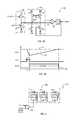
- FIG. 2Ashows a block schematic and timing diagrams of a process monitor circuit that determines the performance of a reference p-channel insulated gate field effect transistor (e.g., PMOS transistor) according to an embodiment.
- a reference p-channel insulated gate field effect transistore.g., PMOS transistor
- FIG. 2Bshows a block schematic and timing diagrams of a process monitor circuit that determines the performance of a reference n-channel insulated gate field effect transistor (e.g., NMOS transistor) according to an embodiment.
- a reference n-channel insulated gate field effect transistore.g., NMOS transistor
- FIG. 2Cshows a block schematic and timing diagram of a process monitor circuit that can select between different reference devices according to an embodiment.
- FIG. 3Ais a block schematic diagram of a pulse extender circuit according to an embodiment.
- FIG. 3Bis a timing diagram showing an operation of a pulse extender circuit like that of FIG. 3A .
- FIG. 4is a block schematic diagram of a counter circuit that can be included in embodiments.
- FIGS. 5A and 5Bare graphs showing the relationship between transistor performance and reverse body bias.
- FIGS. 6A and 6Bare graphs showing the relationship between transistor performance and process variation.
- FIGS. 6C and 6Dare graphs showing process monitor response to reverse body bias voltage and process variation.
- FIGS. 7A to 7Care side cross sectional views of reference transistors that can be included in embodiments.
- FIG. 8is a block schematic diagram of a pulse extender circuit according to an embodiment.
- FIG. 9is a flow diagram of a method according to an embodiment.
- FIG. 10is a block diagram of body bias control system according to an embodiment.
- FIG. 11is a block schematic diagram of body bias control circuits according to an embodiment.
- FIG. 12is a block diagram of a body bias control circuit according to another embodiment.
- Embodimentscan include process monitor circuits that can be used to determine the electrical performance variation of circuit elements that can arise from manufacturing process variations and/or bias conditions.
- circuit elementscan include transistors, and in particular embodiments can include insulated gate field effect transistors, referred to herein as metal-oxide-semiconductor (MOS) transistors, but not implying any particular gate insulator material(s).
- MOSmetal-oxide-semiconductor
- FIG. 1Ashows a functional block diagram of a process monitor circuit 100 that can be included in an integrated circuit (IC) device, in accordance with an embodiment.
- a process monitor circuit 100can include a slew generator circuit 102 , a pulse generator circuit 104 , a pulse extender circuit 106 , and a pulse evaluator 108 .
- a slew generator 102can generate a slew rate signal v 1 having a slew rate that can vary in response to one or more characteristics of reference circuit elements. Such characteristics can be with reference to process “corners”, which can represent process conditions that result in performance extremes of the circuit element(s).
- a reference element 110can be a reference transistor.
- a reference transistorcan be designed to be representative of one or more groups of transistors included on the integrated circuit device (e.g., included in other circuits that provide predetermined functions).
- a slew generator circuit 102can thus use any of a number of different transistors to generate a signal having a slew rate that varies according to the reference transistor 110 .
- slew generatorscan use low threshold voltage (LVT), standard threshold voltage (SVT), or high threshold voltage (HVT) transistor types as a reference transistor (e.g., 110 ) in a process monitor circuit (e.g., 100 ) to monitor the performance of such transistor types.
- LVTlow threshold voltage
- SVTstandard threshold voltage
- HVThigh threshold voltage
- a reference transistore.g., 110
- NMOSn-channel MOS
- MOSp-channel MOS
- a slew rate of the signal v 1can be used to determine the speed and power variation of the one or more group of transistors corresponding to the reference transistor (which is representative of the group of transistors), in the presence of manufacturing process variations.
- an integrated circuitcan include more than one process monitor circuit (e.g., 100 ), where each process monitor circuit includes a slew rate based process monitor circuit that can determine the speed and power variation of a different group of transistors.
- a first slew monitor circuitcan be used to determine the process corner of PMOS transistors on the IC and a second slew monitor can be used to determine the process corner of NMOS transistors on the IC.
- a process monitor circuit 100can use pulse generator circuit 104 to generate monitor data that corresponds to the slew rate of the signal v 1 generated by the slew generator circuit 102 .
- Pulse generator circuit 104may include a ratioed current mirror between PMOS and NMOS transistors, to receive a launch signal to generate a P and N slew, whereupon the slews feed into a selector to charge a capacitor which may discharge to generate a pulse.
- monitor datacan be used as a performance measure of the reference circuit element 110 (e.g., reference transistor).
- the pulse generator circuit 104can receive slew rate signal v 1 and generate a pulse signal v 2 having a pulse, where the duration of the pulse corresponds to the slew rate of the slew rate signal v 1 .
- the duration of a pulse in signal v 2can correspond to the time it takes the slew rate signal v 1 to transition from a first voltage to a second voltage.
- a pulse width of a pulse in signal v 2can be used to determine the speed and power variation of the reference circuit element 110 .
- a pulse extender circuit 106can receive the pulse signal v 2 and generate an extended pulse signal v 3 , which can have an extended pulse with a duration that is proportional to the duration of the pulse provided by pulse signal v 2 .
- the extended pulsehas a longer duration than the duration of the pulse of signal v 2 , and therefore, the duration of the extended pulse can be measured with greater accuracy than the pulse present in pulse signal v 2 .
- the duration of the extended pulse of signal v 3is proportional to that of signal v 1
- the extended pulsealso varies in response to the manufacturing corner of the reference circuit element 110 . Accordingly, the extended pulse can also be used to determine the speed and power variation of the group of transistors that correspond to the reference circuit element 110 .
- a pulse evaluator 108can generate a value corresponding to the duration of the extended pulse of signal v 3 .
- a pulse evaluator 108can be a counter circuit that measures the duration of the extended pulse by counting while the pulse is active.
- an extended pulse signal v 3can be connected to an enable input of a counter circuit, such that the counter circuit increments only when the enable input is asserted. The counter can then increment a count in response to each pulse of a counting clock signal as long as the extended pulse is active.
- a counting clock signalcan be a system clock.
- a resulting count valuecan be a measure of the duration of the extended pulse of signal v 3 .
- FIG. 1Bis a timing diagram that illustrates the operation of process monitor circuit, like that of FIG. 1A , according to a particular embodiment.
- FIG. 1Bshows a slew rate signal v 1 (which can be generated by a slew generator circuit 102 ), a pulse signal v 2 (which can be generated by pulse generator 104 ), and an extended pulse signal v 3 (which can be generated by pulse extender circuit 106 ).
- the slew rate signaltransitions from a first level to a second level over a time interval ⁇ t1 that depends on the performance characteristics of a reference circuit element.
- the pulse voltage signal v 2includes a pulse that corresponds to the slew rate, and in the embodiment shown can be ⁇ t1.
- the extended pulse of signal v 3can have an extended duration ⁇ t2, where the ratio between ⁇ t2 and ⁇ t1 can have a predetermined value. It is understood that any of signals v 1 , v 2 and/or v 3 can represent a signal voltage or current.
- FIG. 1Cis a functional block diagram of a process monitor circuit 100 ′ that can be included in an IC device, in accordance with another embodiment.
- the process monitor circuit 100 ′can include slew generator circuits 102 - 0 to 102 - 5 , a monitor selection multiplexer (MUX) 122 , pulse generator circuit 104 ′, pulse extender circuit 106 ′, and pulse evaluator 108 ′.
- Slew generator circuits( 102 - 0 to 102 - 5 ) can each generate one or more signals having slew rates that correspond to different reference circuit element types.
- slew generator circuits 102 - 0 to 102 - 5utilize as a reference circuit elements a low threshold voltage (LVT) PMOS transistor, a standard threshold voltage (SVT) PMOS transistor, a high threshold voltage (HVT) PMOS transistor, a LVT NMOS transistor, a SVT NMOS transistor, and a HVT NMOS transistor, respectively. It is understood that each of slew generator circuits ( 102 - 0 to 102 - 5 ) can use one or more of the reference transistors to establish the slew of its respective slew rate signal.
- LVTlow threshold voltage
- HVThigh threshold voltage
- each slew generator circuit ( 102 - 0 to 102 - 5 )can include a reference transistor of the type that is being monitored by the respective slew generator.
- the PMOS LVT slew generator circuit 102 - 0can use a PMOS SVT reference transistor
- the NMOS LVT slew generatorcan use an NMOS LVT reference transistor, etc.
- Slew generator circuits ( 102 - 0 to 102 - 5 )generate slew rate signals 124 - 0 to 124 - 5 , respectively.
- a slew rate of each slew rate signal ( 124 - 0 to 124 - 5 )can vary in response to the as fabricated “manufacturing corner” of a corresponding reference transistor of the respective slew generator.
- Multiplexer 122can selectively connect one of the slew generator outputs signals ( 124 - 0 to 124 - 5 ) as an input signal v 1 ′ to the input of the pulse generator circuit 104 ′ in response to a select value SLEW_SELECT.
- Pulse generator circuit 104 ′, pulse extender circuit 106 ′, and pulse evaluator 108 ′can operate in the same, or an equivalent fashion as 104 , 106 and 108 of FIG. 1A . Therefore, in the embodiment of FIG.
- pulse generator circuit 104 ′can be shared across multiple slew generator circuits (e.g., slew generator circuits ( 102 - 0 to 102 - 5 )), thereby reducing the area of the process monitor circuit.
- slew generator circuitse.g., slew generator circuits ( 102 - 0 to 102 - 5 )
- FIG. 2Ais a block schematic diagram of a process monitor circuit 200 -A that can determine the performance of a PMOS transistor, in accordance with an embodiment.
- a process monitor circuit 200 -Acan include a slew generator circuit 202 -A, a pulse generator circuit 204 , and a pulse extender circuit 206 .
- Slew generator circuit 202 -Acan generate a signal v 1 having a voltage with a slew rate that varies according to performance variation in a PMOS reference transistor 210 -A.
- slew generator circuit 202 -Acan include the PMOS reference transistor 210 -A, a current mirror N 20 /N 22 , a load capacitor C 20 , and a reset device P 20 .
- a current mirror N 20 /N 22can mirror a current drawn by PMOS reference transistor 210 -A.
- a reset device P 20which is a PMOS device in the embodiment shown, can charge load capacitor C 20 to a predetermined level.
- a reset signal “RESETB”can be activated (transition low), causing reset device P 20 to charge load capacitor C 20 to an initial voltage. Signal “RESETB” can then return to a high level to turn off reset device P 20 .
- a start signal “start”can then be activated, causing PMOS reference transistor 210 -A to set the magnitude of a reference current provided to current mirror N 20 /N 22 .
- manufacturing process variationscan result in a PMOS reference transistor that is slower or faster (e.g., provides more or less drain current) as compared to a nominal transistor.
- Current mirror N 20 /N 22can discharge load capacitor with a current that mirrors the reference current provided by PMOS reference transistor 210 -A. Therefore, a load capacitor C 20 discharge time can vary in response to the process variations affecting PMOS reference transistor 210 -A.
- Process monitor circuit 200 -Acan measure the slew rate of the voltage across the capacitor (i.e., the slew voltage signal v 1 ) which corresponds to a discharge time of the load capacitor C 20 .
- a measured variation of the discharge time of load capacitor C 20is also a measure of the manufacturing process variation, and process corner of the PMOS reference transistor 210 -A.
- Graph 230positioned below slew generator circuit 202 -A in FIG. 2A , shows one example of a signal v 1 , corresponding to the slew rate of the voltage across load capacitor C 20 .
- signal v 1can be at an initial voltage, and in response to the activation of signal “startb” can fall as load capacitor C 20 is discharged.
- a slew rate signal v 1 output from slew generator circuit 202 -Acan be received by pulse generator circuit 204 .
- Pulse generator circuit 204can generate a pulse signal v 2 having a pulse signal that is active (e.g., high) while signal v 1 is between two reference levels, and low when signal v 1 is outside of the reference levels.
- pulse generator circuit 204can include a first comparator 232 - 0 , second comparator 232 - 1 , and logic 234 .
- Comparators ( 232 - 0 / 1 )can sense slew rate signal v 1 as the load capacitor C 20 is discharging.
- second comparator 232 - 1can be triggered when the slew voltage signal v 1 falls below a second comparator reference voltage VREF2 (e.g., 80% of VDD).
- a first comparator 232 - 0can be triggered (i.e., the output of the comparator transitions from a low to a high voltage level) when the slew rate signal v 1 falls below a first comparator reference voltage VREF1 (e.g., 20% of a high power supply voltage VDD).
- a time interval between the triggering of the first and second comparatorsi.e., the time interval between the slew rate signal v 1 falling from VREF2 to VREF1, is converted into a pulse by logic 234 , which is an XOR logic gate in the embodiment shown.
- Graph 236positioned below pulse generator circuit 204 in FIG. 2A , shows one example of a signal v 2 , corresponding to a pulse output from logic 234 . As shown, signal v 2 can have a pulse of duration of d1.
- a pulse extender circuit 206can extend the duration of a pulse in signal v 2 to generate an extended pulse in a signal v 3 , where the extended pulse has a longer duration that can be measured with enhanced accuracy.
- a pulse extender circuit 206can extend the duration of the pulse in signal v 2 by approximately 100 times in order to create a more easily measured time interval. The operation of various pulse extender circuits (e.g., 206 ) will be described in more detail below in conjunction with FIGS. 3 A/B and 8 .
- a digital countercan count the number of pulses of a clock signal that occur while the extended pulse is active.
- a clock signalcan be generated on the IC device (e.g., by a clock generator) or can be supplied from a source external to the IC device (e.g., by external test equipment).
- Graph 238positioned below pulse extender circuit 206 in FIG. 2A , shows one example of a signal v 3 , corresponding to a signal v 3 output by the pulse extender circuit.
- Signal v 3can have an extended pulse of duration of d2, where d2>d1.
- FIG. 2Bshows a process monitor circuit 200 -B that can determine the performance of an NMOS transistor, in accordance with one embodiment.
- Process monitor circuit 200 -Bcan include a slew generator circuit 202 -B, a pulse generator circuit 204 , and a pulse extender circuit 206 .
- Slew generator circuit 202 -Bcan generate a signal v 1 ′ having a voltage with a slew rate that varies according to performance variation in a NMOS reference transistor 210 -B.
- slew generator circuit 202 -Bcan include the NMOS reference transistor 210 -B, a current mirror P 24 /P 26 , a load capacitor C 20 , and a reset device N 24 .
- a current mirror P 24 /P 26can mirror a current drawn by PMOS reference transistor 210 -B.
- a reset device N 24which is a NMOS device in the embodiment shown, can discharge load capacitor C 20 to a predetermined level.
- a reset signal “RESET”can be activated (transition high), causing reset device N 24 to discharge load capacitor C 20 to an initial voltage. Signal “RESET” can then return to a low level to turn off reset device N 24 .
- a start signal “start”can then be activated, causing NMOS reference transistor 210 -B to set the magnitude of a reference current drawn from current mirror P 24 /P 26 .
- manufacturing process variationscan result in a NMOS reference transistor that is slower or faster (e.g., provides more or less drain current) as compared to a nominal transistor.
- Current mirror P 24 /P 26can charge load capacitor C 20 with a current that mirrors the reference current drawn by NMOS reference transistor 210 -B. Therefore, a load capacitor C 20 charge time can vary in response to the process variations affecting NMOS reference transistor 210 -B.
- Process monitor circuit 200 -Bcan measure the slew rate of the voltage across the capacitor (i.e., the slew voltage signal v 1 ′) which corresponds to a charge time of the load capacitor C 20 .
- a measured variation of the charge time of load capacitor C 20is also a measure of the manufacturing process variation, and process corner of the NMOS reference transistor 210 -A.
- Graph 230 ′positioned below slew generator circuit 202 -B in FIG. 2B , shows one example of a signal v 1 ′, corresponding to the slew rate of the voltage across load capacitor C 20 .
- signal v 1 ′can be at an initial voltage, and in response to the activation of signal “start” can rise as load capacitor C 20 is charged.
- a slew rate signal v 1 ′ output from slew generator circuit 202 -Bcan be received by pulse generator circuit 204 .
- Pulse generator circuit 204can operate like that of FIG. 2A , generating a pulse signal v 2 having a pulse signal that is active (e.g., high) while signal v 1 ′ is between two reference levels, and low when signal v 1 ′ is outside of the reference levels.
- first comparator 232 - 0can be triggered (i.e., the output of the comparator transitions from a low to a high voltage level) when the slew rate signal v 1 ′ rises to a first comparator reference voltage VREF1 (e.g., 20% of a high power supply voltage VDD).
- Second comparator 232 - 1can be triggered when the slew voltage signal v 1 ′ rises to a second comparator reference voltage VREF2 (e.g., 80% of VDD).
- a time interval between the triggering of the first and second comparatorsi.e., the time interval between the slew rate signal v 1 ′ rising from VREF1 to VREF2, is converted into a pulse by logic 234 , which is an XOR logic gate in the embodiment shown.
- Graph 238 ′positioned below pulse extender circuit 206 in FIG. 2B , shows one example of a signal v 3 ′, corresponding to a signal v 3 ′ output by the pulse extender circuit.
- signal v 3 ′can have an extended pulse of duration of d2′, where d2′>d1′.
- a pulse extender circuit 206can operate in the same or equivalent manner as that shown as 206 in FIG. 2A . Further, though not shown in FIG. 2B , in some embodiments, a digital counter can count the number of pulses of a clock signal that occur while the extended pulse is active, as noted above.
- Graph 238 ′positioned below pulse extender circuit 206 in FIG. 2B , shows one example of a signal v 3 ′, corresponding to a signal v 3 ′ output by the pulse extender circuit.
- signal v 3can have an extended pulse of duration of d2′, where d2′>d1′.
- FIG. 2Cshows a process monitor circuit 200 -C that can determine the performance of different transistor types, including transistors of different conductivity types.
- Process monitor circuit 200 -Ccan include multiple slew generator circuits (two shown as 202 -C and 202 - n ), each including a different reference transistor (e.g., 210 -C and 210 - n ).
- process monitor circuit 200 -Ccan include a slew generator circuit 202 -C that determines the performance of a PMOS reference transistor 210 -C and a slew generator circuit 202 - n that determines the performance of a NMOS reference transistor 210 - n.
- Slew rate signals v 1 -C and v 1 - n output from the slew generator circuitscan have slew rates that vary according to their reference circuit element (e.g., NMOS or PMOS transistors) performance variations.
- a MUX 222can selectively connect one of the slew rate signals (e.g., v 1 - 0 and v 1 - n ) to a pulse generator 204 .
- a pulse generator circuit 204 and pulse extender circuit 206can operate in the same or equivalent manner as that shown as 204 and 206 in FIG. 2A . Further, though not shown in FIG. 2C , in some embodiments, a digital counter can count the number of pulses of a clock signal that occur while the extended pulse is active, as noted above.
- a charging or discharging time of a load capacitor as described hereincan be extended to enhance the accuracy of a process monitor measurement.
- a ‘typical’ target for the load capacitor charging/discharging timecan be about 40 ns, although charging/discharging times can vary due to manufacturing process variation.
- a charging/discharging time that is too shortcan make it more difficult to design comparators (e.g., 232 - 0 / 1 ) within pulse generator circuits (e.g., 204 ), as they must be fast and precise enough to capture the signal slew.
- a pulse generator circuite.g., 204
- a pulse extender circuite.g., 206
- a very short pulsemay not inject enough charge into the capacitor of the pulse extender circuit (e.g., 206 ) to generate an extended pulse of sufficient duration for accurate measurement by a counter circuit, or the like.
- an extended load capacitor charging timecan reduce the area required to implement a process monitor circuit, and increase the accuracy of the process monitor measurement (e.g., measured duration of a pulse or extended pulse).
- a load capacitor charging/discharging timeis extended by reducing the current that charges/discharges the load capacitor, (e.g., a current mirrored current by a current mirror N 22 /N 24 , P 24 /P 26 ).
- One method of reducing the mirrored currentcan be to reduce the reference current of the current mirror, i.e., the current flowing through the reference transistor (e.g., 210 -A/B).
- a mirrored currentcan be reduced by setting the relative transistor sizes of the current mirror (i.e., the width to length ratios of the two transistors) such that the current flowing through the load capacitor (i.e., the mirrored current) is a small fraction of the reference current for the current mirror. Reducing the mirrored current can also be used in certain embodiments to reduce the size of the load capacitor while still maintaining an acceptable capacitor charging time that can be accurately measured by the process monitor.
- the reference currentis also reduced by implementing the reference transistor (e.g., 210 -A/B) as a minimum channel length transistor composed of many fingers.
- a minimum length transistorcan be a length substantially similar to the channel length used for logic transistors in the same IC.
- Such a reference transistorcan provide a reduced reference current that is substantially insensitive to random process variations.
- a current mirrorN 22 /N 24 , P 24 /P 26 ) can be implemented using transistors that are substantially insensitive to process variation, and the two transistors can be sized to provide a mirrored current that is a small fraction of the reference current.
- FIG. 3Ashows a pulse extender circuit 306 , in accordance with an embodiment.
- a pulse extender circuit 306can be one version of those shown as 206 in FIGS. 2A to 2C .
- a pulse extender circuit 306can include an extender capacitor C 30 , an input-to-voltage integrator 346 , a proportional discharge circuit 348 , a comparator 340 , and logic 342 .
- An input-to-voltage integrator 346can provide a fixed current (I/100) to charge capacitor C 30 .
- input-to-voltage integrator 346can include a current mirror P 32 /P 34 and an enable device N 32 .
- Current mirror P 32 /P 34can have one leg connected to capacitor C 30 and the other connected to enable device N 32 .
- the PMOS transistor P 32 of the current mirror P 32 /P 34 which supplies current to capacitor C 30can be substantially smaller than the other PMOS transistor P 34 , to provide a relatively small, but accurate current to capacitor C 30 .
- Enable device N 32can enable the current mirror P 32 /P 34 in response to the output of logic 342 .
- Proportional discharge circuit 348can discharge capacitor C 30 by an amount proportional to an input signal pulse duration.
- the amount by which capacitor C 30 is dischargedcan reflect the performance of a reference circuit element, such as a PMOS or NMOS transistor, as described herein, or equivalents.
- proportional discharge circuit 348can include a discharge device N 30 and a reset device P 30 .
- a discharge device N 30can be an NMOS transistor with a source-drain path connected between capacitor C 30 and a low voltage (e.g., low power supply voltage VSS), and a gate that receives an input pulse (Input) (such as an input pulse from a pulse generator circuit as described herein, or an equivalent).
- a reset device P 30can be a PMOS transistor having a source-drain path connected between a high voltage (e.g., a high reference voltage V1) and capacitor C 30 , and a gate that receives a reset pulse.
- a current sunk by discharge device N 30can be substantially greater than that provided by input-to-voltage integrator 346 .
- a current sunk by discharge device N 30can be I, i.e., 100 ⁇ that provided by the current mirror P 32 /P 34 .
- Comparator 340can compare the voltage across the capacitor C 30 (shown as V2) to the high reference voltage V1. Thus, when V2 ⁇ V1, the comparator 340 can have an active output value. When V2>V1, the comparator 340 can have an inactive output. In response to an active output from comparator 340 , logic 342 can generate an output value “Output” that is high, enabling input-to-voltage integrator 346 . In one particular embodiment, logic 342 can be a flip-flop circuit.
- FIG. 3Bis a timing diagram showing an operation of a pulse extender circuit like that of FIG. 3A .
- FIG. 3Bincludes the waveforms V1 (reference input to comparator 340 ), V2 (voltage across capacitor C 30 ), Input (input signal to discharge device N 30 ) and Output (output signal from logic 342 ).
- capacitor C 30can be charged to a voltage V1.
- signal Inputcan pulse high.
- a voltage of capacitor C 30can start to discharge.
- a pulse duration of input signal Inputcan be d1.
- the pulseends, and discharge device N 30 turns off.
- the amount by which capacitor C 30 dischargesis thus proportional to the duration d1.
- d1can reflect the performance of a reference circuit element (e.g., transistor) thus, V1-V2 corresponds to a performance value of the reference circuit element.
- comparator 340can activate its output and logic 342 can set the value of Output high, starting the extended pulse. Input-to-voltage integrator 346 can be enabled, and thus start to charge C 30 back toward V1.
- the charge current provided by current mirror P 32 /P 34can be 1/100 of the original pulse current provided by discharge device N 30 . Since the charge current is set to 1/100 of the discharging current, the extended pulse output from logic 342 can be 100 times the pulse width of the original pulse on signal Input. It is noted that the 100 ⁇ proportionality can depend on the matching of current mirrors, and not the actual values of the currents or capacitance. As such, this proportionality is not affected very much by process corner.
- the capacitor discharge time for discharging from a first predetermined voltage V2 to a second voltage in response to the input voltage pulseis shorter than the time duration for charging the capacitor to the first predetermined voltage V1.
- FIGS. 3 A/Bshow the generation of an extended pulse based on an initial discharge and subsequent charging of a capacitor
- alternate embodimentscan be based on an initial charge and subsequent discharge of a capacitor.
- FIG. 4is a block schematic diagram of a counter circuit 408 , in accordance with one embodiment.
- a counter circuit 408can be one particular implementation of a pulse evaluator circuit, like that shown as 108 in FIG. 1A .
- an output of a pulse generator circuit or a pulse extender circuitcan act as an enable input to a counter circuit 408 .
- Counter circuit 408can increment a count value every time there is a pulse in a counting clock signal, as long as an input pulse is active.
- a counter circuit 408can include counter 440 and control logic 444 .
- Counter 440can include flip flops 442 - 0 to 442 - i with corresponding inverters (I 40 ) arranged in series, with each flip flop ( 442 - 0 to 442 - i ) representing a bit of a count value.
- Logic 444can generate pulses as clock inputs to a least significant bit flip flop 442 - 0 . As noted above, as long as an extended pulse input (Pulse Extender Output) is active (high in the example shown), logic 444 can generate a pulse corresponding to each pulse of CLK_CNT. Thus, a resulting count value stored by counter 440 can correspond to a duration of the pulse from Pulse Extender Output.
- a typical clock available from test equipment used during manufacturing testcan be 25 MHz. Given a 40 ns typical pulse width, and a 100 ⁇ extension of the pulse width, a 25 MHz clock can generate a count of 100 for a typical corner.
- a count value generated by a counter circuite.g., 408
- process monitor circuits described herein, and equivalentscan be advantageously used to measure the variation of performance characteristics of integrated circuit devices in the presence of manufacturing process variations.
- Such process monitor circuitscan advantageously provide a digitally readable measurement that allows process variation measurements without the use of special test equipment.
- the digital measurements provided by such process monitorscan be read out without using any additional pins (e.g., using a scan chain or a register interface logic), and the digital measurements can be performed during normal operation of the integrated circuit and during power up.
- Process monitor circuits described herein, and equivalentscan also be used to measure the variation of PMOS and NMOS transistors separately, and therefore, can enable independent determination of the PMOS and NMOS transistor manufacturing process corners.
- Process monitor circuits as described herein, or equivalentscan also be used to measure the variation of different transistor types separately, e.g., the manufacturing corners of LVT, SVT, and HVT transistors can be independently determined by using process monitors having a representative LVT, SVT, and HVT transistor respectively.
- the process monitor circuits as described herein, or equivalentscan be substantially insensitive to random variations of transistor performance characteristics, such as random dopant fluctuation, which can skew the process monitor measurements and introduce errors in determining the systematic manufacturing process variations.
- the process monitors described abovecan be used to determine process corners during a manufacturing test, since the process monitor measurement can be performed in a short time.
- a body bias control circuitcan adjust the body bias voltage for one or more groups of transistors in an IC device to provide a predetermined target transistor performance in the presence of manufacturing process variations.
- Such body bias control circuitscan use the process monitor circuits described herein, or equivalents, to determine the manufacturing process corner and to adjust the body bias voltage to compensate for resulting transistor performance variations.
- performance data generated by such process monitor circuitscan be used to measure the transistor speed variation resulting from manufacturing process variations, and the body bias voltage can be adjusted in response to the monitor data to obtain a target transistor speed.
- the target transistor speedis used to determine a target monitor data value, and the body bias voltage is adjusted until the monitor data measured by the process monitor is substantially equal to the target monitor data value.
- process monitor circuits as described herein, or equivalentscan be used as part of a continuous feedback system, where such a process monitor circuit is used as a body bias monitor that monitors transistor performance as the body bias voltage is adjusted to achieve target transistor performance in order to compensate for manufacturing process variations.
- Such process monitor circuitspreferably have a smooth and predictable response to body bias voltage.
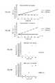
- FIG. 5Ais a graph showing an NMOS process monitor circuit response, according to an embodiment, where the process monitor circuit utilizes an NMOS reference transistor.
- FIG. 5Ashows a resulting output count (i.e., extended pulse width duration) for various reverse body bias voltages. It is noted from the figure that the response to NMOS bias voltage is substantially smooth and linear, while the response to the PMOS bias voltage is substantially zero.
- FIG. 5Bis a graph showing a PMOS process monitor circuit response, according to an embodiment, where the process monitor circuit utilizes a PMOS reference transistor.
- FIG. 5Bshows a resulting output count (i.e., extended pulse width duration) for various reverse body bias voltages. It is noted from the figure that the response to PMOS bias voltage is substantially smooth and linear, while the response to the NMOS bias voltage is substantially zero.
- process monitor circuitscan be used to independently adjust body bias voltages for NMOS and PMOS transistors to compensate for transistor performance variations.
- process monitor circuitscan also be used to monitor transistor performance and compensate for transistor performance due to other factors, such as operating temperature, aging of the IC device.
- monitoringcan be continuous during the operation of the IC. More specifically, although the descriptions herein are in the context of monitoring performance variation in transistors due to manufacturing process-related effects, the same circuits in the embodiments or the equivalents can be used to monitor performance variation due to any appropriate cause.
- process monitorcan refer generally to monitoring circuits that identify transistor performance characteristics that may be a result of process drifts or other factors that may affect transistor performance. “Process monitor” is not limited to a circuit that monitors variations arising from semiconductor processing. “Process corner” is not limited to semiconductor process-related characteristics. Rather, “process corner” is any characterization of a transistor performance in a given context, whether speed, leakage or other characteristic arising from anything that can cause a variation in transistor performance from nominal.
- the PMOS and NMOS process monitor circuitscan be used to determine the process corner of the PMOS and NMOS reference transistors that are used by the respective process monitor circuits. Such operations are represented by graphs in FIGS. 6A and 6B .
- FIG. 6Ais a graph showing how a PMOS process monitor circuit response can be used to determine the manufacturing process corner of the reference PMOS transistor.
- the vertical axis of the graphshows the “relative slew rate to TT” (hereinafter referred to as “relative PMOS slew rate”), which is measured as the ratio of the slew rate measured by the PMOS process monitor to the slew rate for the TT (typical NMOS and typical PMOS) process corner.
- the relative PMOS slew rateis different for different PMOS process corners, i.e., the relative PMOS slew rate is substantially different for the FF/SF corners (corresponding to fast PMOS process corners), the TT corner, and the FS/SS corners (corresponding to slow PMOS process corners). It is also noted that the PMOS slew rate and the PMOS process monitor performance is substantially independent of the NMOS process corner. Therefore, the relative PMOS slew rate can be used to determine the PMOS process corner.
- FIG. 6Bis a graph showing how the NMOS process monitor response can be used to determine the manufacturing process corner.
- the vertical axis of the graphshows the “relative slew rate to TT” (hereinafter referred to as “relative NMOS slew rate”), which is measured as the ratio of the slew rate measured by the NMOS process monitor to the slew rate for the TT (typical NMOS and typical PMOS) process corner.
- the relative NMOS slew rateis different for different NMOS process corners, i.e., the relative NMOS slew rate is substantially different for the FF/FS corners (corresponding to fast NMOS process corners), the TT corner, and the SF/SS corners (corresponding to slow NMOS process corners). It is also noted that the NMOS slew rate and the NMOS process monitor performance is substantially independent of the PMOS process corner. Therefore, the relative NMOS slew rate can be used to determine the NMOS process corner.
- FIG. 6Cis a graph showing a response of a PMOS process monitor circuit, according to an embodiment, to reverse body bias voltages at different process corners.
- the graphshows the measured slew rate as a function of PMOS reverse bias voltage for three different process corners, SS (slow NMOS and PMOS), TT (typical NMOS and PMOS), and FF (fast NMOS and PMOS).
- FIG. 6Dis a graph showing a response of a NMOS process monitor circuit, according to an embodiment, to reverse body bias voltages at different process corners.
- the graphshows the measured slew rate as a function of NMOS reverse bias voltage for three different process corners, SS (slow NMOS and PMOS), TT (typical NMOS and PMOS), and FF (fast NMOS and PMOS).
- the NMOS and PMOS transistor performance in the SF (slow NMOS, fast PMOS) cornerare substantially identical to the NMOS transistor performance in the SS (slow NMOS, slow PMOS) corner, and the PMOS transistor performance in the FF (slow NMOS, fast PMOS) corner, respectively.
- the NMOS and PMOS transistor performance in the FS corner of the square process cornersare substantially identical to the NMOS transistor performance in the FF corner and the PMOS transistor performance in the SS corner.
- the following tableillustrates the difference between the conventional process corners and the square process corners, where the “+” table entry indicates a smaller change in transistor electrical characteristics as compared to the change corresponding to the “+++”.
- process monitor circuits and body bias control circuits as described herein and equivalentscan be used to monitor any suitable circuit element type, particular embodiments can be included in ICs having transistor with high body coefficients. Examples of such transistors will now be described.
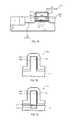
- FIG. 7Ashows a deeply depleted channel (DDC) type transistor 770 , which can be included in embodiments.
- a DDC transistor 770can be a reference transistor that is monitored to reflect the performance of like DDC transistors 770 in an IC device.
- a DDC transistor 770can be configured to have an enhanced body coefficient, along with the ability to set a threshold voltage (Vt) with enhanced precision.
- a DDC transistor 770can include a gate electrode 782 , source 784 , drain 786 , and a gate dielectric 788 positioned over a substantially undoped channel 711 .
- a gate electrode 782can have spacers 792 formed in its sides.
- Optional lightly doped source and drain extensions (SDE) 790can be positioned respectively adjacent to source 784 and drain 786 . Such extensions 790 can extend toward each other, reducing effective length of the substantially undoped channel 711 .
- a body bias voltagecan be applied to a well 717 via a body tap 783 .
- the DDC transistor 770is shown as an n-channel transistor having a source 784 and drain 786 made of n-type dopant material, formed upon a substrate such as a p-type doped silicon substrate providing a p-well 717 .
- the n-channel DDC transistor 770 in FIG. 7Acan include a highly doped screening region 715 made of p-type dopant material, and a threshold voltage set region 713 made of p-type dopant material.
- FIG. 7Bshows FinFET type transistor 770 -B which can be included in embodiments as a reference circuit element corresponding to like elements in an IC device.
- the FinFET transistor 770 -Bcan include a gate electrode 782 -B and gate dielectric 788 -B formed on opposing sides of a substantially undoped channel 711 -B.
- the view of FIG. 7Bis taken along a channel length. Thus, it is understood that source and drain regions can extend into and out of the view shown.
- FIG. 7Cshows a FinFET type transistor 770 -C having a screening region 715 -C which can be included in embodiments.
- the FinFET transistor 770 -Ccan have a screening region which can be configured to have an enhanced body coefficient, along with the ability to set a Vt with enhanced precision.
- the transistor 770 -Cincludes a gate electrode 782 -C and gate dielectric 788 -C formed over a substantially undoped channel 711 -C on opposing sides.
- a highly doped screening region 715 -Cis formed in a substrate 719 below substantially undoped channel 711 -C.
- a Vt set region 713 -Cis formed between the screening region 715 -C substantially undoped channel 711 -C.
- the view of FIG. 7Cis taken along a channel length, and source and drain regions can extend into and out of the view, separated from screening region 715 -C by portions of undoped channel region 711 -C.
- Embodiments of various structures and manufacturing processes suitable for use in DDC transistorsare disclosed in U.S. Pat. No. 8,273,617, issued on Sep. 25, 2012, titled “Electronic Devices and Systems, and Methods for Making and Using the Same”, by Scott E. Thompson et al.; U.S. Pat. No. 8,530,286 issued on Sep. 10, 2013 titled “Low Power Semiconductor Transistor Structure and Method of Fabrication Thereof”; U.S. patent application Ser. No. 12/971,955 filed on Dec. 17, 2010 titled “Transistor with Threshold Voltage Set Notch and Method of Fabrication Thereof”; U.S. patent application Ser. No. 12/895,785 filed on Sep.
- conductivities of any of the transistors described abovecan be switched (i.e., from p-channel to n-channel and vice versa).
- the process and bias monitor circuits discussed aboveare advantageously used in IC devices that are implemented using DDC transistors having an enhanced body coefficient as compared to conventional nanoscale devices.
- the response of the DDC transistorcan vary within a wider range to a change in the body bias voltage applied to the screening region. More specifically, the enhanced body coefficient of the DDC transistor can allow a broad range of ON-current and OFF-current that depends on the body bias voltage applied to the screening region, as compared to the body bias voltage applied to a conventional device.
- the DDC transistorshave a better transistor matching coefficient (AVT), i.e., a lower threshold variation ( ⁇ V T ) than conventional devices.
- AVTtransistor matching coefficient
- ⁇ V Ta lower threshold variation
- the lower ⁇ V Tprovides a lower minimum operating voltage VDD and a wider range of available nominal values of V T .
- the enhanced body coefficient of the DDC transistorcan also allow a broad range of threshold voltage that depends on the body bias voltage applied to the screening region, as compared to the body bias voltage applied to a conventional device.
- the screening regionallows effective body biasing for enhanced control of the operating conditions of a device or a group of devices to be set by controlling the applied body bias voltage.
- different operating conditionscan be set for devices or groups of devices as a result of applying different body bias voltages.
- embodimentscan include pulse extender circuits that rely on the discharging/charging of a capacitor, like that shown in FIG. 3A
- other embodimentscan include digital pulse extender circuits.
- digital pulse extender circuitsVarious embodiments of digital pulse extender circuits will now be described.
- Digital pulse extender circuitscan be used to generate an extended pulse signal having an extended pulse duration that is longer than the pulse duration of a received input pulse signal. There can be a predetermined ratio between the extended pulse duration and the input pulse duration.
- FIG. 8shows a digital pulse extender circuit 806 , in accordance with one embodiment.
- Pulse extender circuit 806can receive an input signal (pulse — 1 ⁇ ) that can include an input pulse, and can generate an extended pulse on an output signal (pulse — 128 ⁇ ).
- an extended pulse durationcan be approximately some power of two (e.g., 2 7 ) times the pulse duration of pulse — 1 ⁇ .
- a pulse extender circuit 806can receive input signal pulse — 1 ⁇ , which can include a pulse having a duration reflecting a circuit element performance, a clock input (r_clk), which can be a clock signal generated by a ring oscillator 880 , and can output an extended pulse signal pulse — 128 ⁇ .
- Pulse extender circuit 806can include a first frequency divider 882 , a second frequency divider 884 , a digital comparator 886 , a MUX 888 , output logic 890 , and input logic 892 .
- a pulse extender circuit 806can include a calibration MUX 894 for selectively inputting the input signal pulse pulse — 1 ⁇ or a calibration pulse (cal_pulse) according to a signal CALIB.
- First frequency divider 882can divide an input pulse according to clock signal r_clk to generate a count value corresponding to the duration of an input pulse of signal pulse — 1 ⁇ .
- first frequency divider 882can be a digital counter, and by operation of input logic 892 , can receive clock signal r_clk as a clock input and pulse — 1 ⁇ signal as an enable signal.
- the countercan increment a count value while the pulse — 1 ⁇ signal is active (e.g., at a high logic level in FIG. 8 ).
- the value of the count in the counteris representative of the pulse duration of pulse — 1 ⁇ , as measured by the number of ring oscillator clock cycles within duration of the pulse — 1 ⁇ signal.
- the countercan be a 12-bit counter.
- Second frequency divider 884can also divide according to count clock r_clk. However, second frequency divider 884 can count for a multiple of the count value generated by first frequency divider 882 . In the embodiment shown, second frequency divider 884 can also be a counter circuit. Second frequency divider 884 can start counting when the pulse — 1 ⁇ signal transitions to a high logic level, and can stop counting when the count value of the second frequency divider is some multiple (e.g., 128 times) the count in the first frequency divider 882 . In one particular embodiment, such a second frequency divider can be implemented as a 19-bit counter, while the first frequency divider can be a 12-bit counter. A count value of the 19-bit counter can be representative of 128 times the pulse duration of the pulse — 1 ⁇ pulse duration, as measured by the number of ring oscillator clock cycles within the pulse — 128 ⁇ signal.
- digital comparator 886can receive a count from the first frequency divider 882 as a first input, and a count from the second frequency divider 884 as a second input (labeled in the figure as div12 and div19, respectively, in FIG. 8 ). Digital comparator 886 can assert an output signal “match” if the seven least significant bits of div19 are zero, and bits 7 through 18 of div19 are equal to bits 0 through 12 of div12, respectively. Therefore, the match signal is asserted when the count from the second divider is 128 times the count from the first divider.
- the extended pulse signal pulse — 128 ⁇can be asserted when either pulse — 1 ⁇ or pulse — 128 ⁇ is at a high logic level, and it can be de-asserted once the match signal is asserted.
- the extended pulse signal pulse — 128 ⁇can be generated by operation of MUX 888 and logic 890 (which can be a FF).
- second frequency divider 884can receive count clock r_clk as a clock input and the extended pulse signal pulse — 128 ⁇ as an enable signal, such that the second frequency divider increments a count based on r_clk while pulse — 128 ⁇ signal is at a high logic level.
- digital pulse extender circuit 806can also operate in an optional calibration mode, where a calibration pulse input cal_pulse having a predetermined pulse width is selectively input to the digital pulse extender circuit 806 when the calibrate input CALIB to calibration MUX 894 is asserted.
- the pulse width of the extended pulse signalwill be a multiple of the pulse width of the calibration pulse input (cal_pulse).
- cal_pulsethe pulse width of the extended pulse signal.
- a pulse width of the extended pulse signalis 128 times the pulse width of an input pulse of signal cal_pulse.
- a pulse width of the extended pulse signalcan be measured to verify and calibrate the operation of the digital pulse extender circuit.
- a digital pulse extender circuit 806can operate correctly and generate an extended pulse signal for a range of counting clock frequencies (e.g., ring oscillator output frequencies).
- a ring oscillator output frequencycan be selected to be sufficiently high such that multiple ring oscillator cycles can fit within the pulse width of the input pulse signal pulse — 1 ⁇ .
- the ring oscillator output frequencycan be set to 2 GHz such that 50 to 80 ring oscillator cycles, respectively, can fit within the pulse width of the pulse — 1 ⁇ signal.
- first and/or second dividershaving different numbers of bits to generate an extended pulse signal having a duration that is a different multiple of the input pulse duration.
- Embodiments of the digital pulse extender circuit described abovecan be used as part of a process monitor circuit, as described herein or equivalents, where such process monitor circuit generates a slew signal that depends on electrical characteristics of one or more representative circuit elements, such as NMOS or PMOS transistors. Such a signal slew can be converted into a pulse signal. Such a pulse signal can be provided as an input (e.g., pulse — 1 ⁇ ) to a digital pulse extender circuit 806 .
- Such process monitor circuitscan be used to determine the electrical performance variation of the different transistor types as a result of manufacturing process or other sources of transistor variation.
- FIG. 9is a flow diagram of a method 900 according to an embodiment.
- a method 900can generate body bias voltages based on process monitoring circuits, like those disclosed herein, or equivalents.
- a method 900can include providing circuit elements for measuring variability according to process and/or operation conditions ( 902 ).
- Such an actioncan include providing circuit elements such as transistors of different conductivity types, including DDC type transistors, reflecting the performance variability arising from fabrication process and/or operating conditions. Monitor values can be generated reflecting performance dominating variations ( 904 ).
- Such an actioncan include generating monitoring values from the provided circuit elements corresponding to “corner” conditions. In particular embodiments, this can include generating a slew based monitor value as described herein, or equivalents.
- such an actioncan further include deriving biasing conditions, such as body bias values, that can compensate for corner conditions.
- a method 900can measure performance of preselected circuit elements for performance values ( 906 ). In some embodiments, this can include generating slew rate performance values for particular transistors of an IC device, as described herein, or an equivalent. Performance values can be compared to monitored values to generate operating points ( 908 ). In a very particular embodiment, such an action can include determining the corner conditions of transistors of an IC device (based on a set of previously generated monitored values). Such conditions can be compared to a desired performance.
- a method 900can generate body bias settings based on the operating points to establish the performance of a device ( 910 ). Such an action can include generating body bias voltages for groups of transistors based on a slew rate corresponding to a reference transistor of the same type. The body bias voltages can be applied in the device according to the body bias settings ( 912 ). Such an action can include the static application of body bias voltages, or the dynamic application of body bias voltages based on operational mode, temperature conditions, etc.
- FIG. 10shows an IC device 1000 according to another embodiment.
- An IC device 1000can include various sections 1003 - 0 to 1003 - 2 , any of which can include one or more body bias generator circuits that apply an adjustable body bias to various transistors.
- a value of such body bias voltagescan be derived from a performance monitor values, including slew based performance monitor values as described herein, or equivalents.
- IC device 1000can include a first section 1003 - 0 that includes a first charge pump 1005 -N and a second charge pump 1005 -P.
- a first charge pump 1005 -Ncan generate a global body bias voltage Vpump1 for n-channel transistors.
- a second charge pump 1005 -Pcan generate a global body bias voltage Vpump2 for p-channel transistors.
- Such global body bias voltages (Vpump1/2)can be provided to each section ( 1003 - 0 to ⁇ 2).
- first and second charge pumps ( 1005 -N/P)can generate global body bias voltages in response to a charge pump clock signal CLK_CP.
- Each section ( 1003 - 0 to ⁇ 2)can include one or more body bias generator circuits which can apply a body bias voltage to a group of transistors having a level established by bias set values.
- bias set valuescan be generated using slew-based monitored values, as described herein, or equivalents.
- body bias set valuescan be generated as described for block 910 in FIG. 9 .
- IC device 1000can include an analog section 1003 - 0 , a digital section 1003 - 1 , and a memory section 1003 - 2 .
- An analog section 1003 - 0can include an n-channel transistor body bias generator circuit 1007 - 0 , which can generate a body bias for n-channel transistors of section 1003 - 0 based on bias set values set_biasN0 and using global body bias Vpump1.
- an analog section 1003 - 0can also include a p-channel transistor body bias generator circuit 1009 - 0 , which can generate a body bias for p-channel transistors of section 1003 - 0 based on bias set values set_biasP0 and using global body bias Vpump2.
- Digital section 1003 - 1can include body bias generator circuits like section 1003 - 0 , but can include many more such circuits to enable different body biases for different circuit sections.
- N-channel body bias generator circuitsare shown as 1007 - 00 to 0x, and each receive different bias set values set_biasN1.
- P-channel body bias generator circuitsare shown as 1009 - 00 to 0y and each receive different bias set values set_biasP1.
- Memory section 1003 - 2can include body bias generator circuits like section 1003 - 0 , but can include two more such circuits to enable different body biases for different circuit sections.
- N-channel body bias generator circuitsare shown as 1007 - 10 to 1z, and each receive different bias set values set_biasN2.
- P-channel body bias generator circuitsare shown as 1009 - 10 to 1w and each receive different bias set values set_biasP2.
- bias set valuescan be digital values.
- charge pump 1005 -Ncan generate a global bias voltage Vpump1 that is lower than the ground supply level of the IC device 1000
- charge pump 1005 -Pcan generate a global bias voltage Vpump2 that is higher than the power supply level of the IC device 1000
- a clock signal CLK_CPcan operate at some nominal frequency (e.g., 25 MHz) but can be programmed or selected to operate at a higher or lower frequency.
- any or all of the various bias set valuescan be generated in response to a slew based process monitor circuit as described herein, or an equivalent.
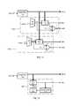
- FIG. 11shows examples of a body bias generator circuits 1100 - 0 / 1 according to an embodiment.
- Body bias generator circuits ( 1100 - 0 / 1 )can each use a low dropout regulator circuit (LDO) ( 1111 ) to generate body bias voltages (Vbn1, Vbn2) that are fractions of a global body bias voltage Vpump.
- LDOlow dropout regulator circuit
- a global body bias voltage Vpumpcan be provided by a voltage source 1105 , which can be a charge pump, or the like.
- operating points for each LDO 1111can be established by a bias set values (set1[x:0], set2[x:1]).
- bias set valuesset1[x:0], set2[x:1]
- DACdigital-to-analog converters
- LDOs 1111can force their body bias voltages (Vbn1, Vbn2) to match the analog control values (actrl1, actrl2).
- bias set values[set1[x:0], set2[x:1]) can be generated in response to slew based monitor values generated as described herein, and equivalents.
- each body bias generator circuit 1100 - 0 / 1can include a comparator 1113 which can generate a lock signal (lock 1 , lock 2 ) once a body bias voltage (Vbn1, Vbn2) matches its corresponding analog control value (actrl1, actrl2).
- FIG. 12shows examples of a body bias generator circuit 1200 according to another embodiment.
- Body bias generator circuit 1200can control a body bias voltage based with a self-calibrating, continuous feedback control system.
- a feedback loopcan include a process monitor circuit, such a slew-based process monitor circuit as described herein.
- body bias generator circuit 1200can include an LDO 1211 , process monitor circuit 1217 , and a feedback circuit 1219 , which in a particular embodiment, can be a proportional-integrator-derivative (PID) controller.
- LDO 1211can establish a body bias voltage Vbn based on an analog control value actrl using a global body bias voltage Vpump from a voltage source, such as a charge pump 1205 .
- a process monitor circuit 1217can include one or more slew based process monitor circuits as described herein, or an equivalent.
- a generated body bias voltage Vbncan be applied to one or more reference elements within process monitor circuit 1217 .
- the performance of the reference elementcan be monitored. If performance does not meet a target value, feedback circuit 1219 can adjust an analog control signal (actrl) to adjust a bias voltage to bring circuit element performance toward a desired value. Such feedback can continue until a reference circuit element meets a desired performance.
- wafers and die supporting multiple transistor typesincluding those with and without the described dopant layers and structures are contemplated for use with the embodiments and equivalents.
- Electronic devices that include the disclosed transistor structures or are manufactured in accordance with the disclosed processescan incorporate die configured to operate as “systems on a chip” (SoC), advanced microprocessors, radio frequency, memory, and other die with one or more digital and analog transistor configurations, and are capable of supporting a wide range of applications, including wireless telephones, communication devices, “smart phones”, embedded computers, portable computers, personal computers, servers, and other electronic devices.
- SoCsystem on a chip
- Electronic devicescan optionally include both conventional transistors and transistors as disclosed, either on the same die or connected to other die via motherboard, electrical or optical interconnect, stacking or through used of 3D wafer bonding or packaging. According to the methods and processes discussed herein, a system having a variety of combinations of analog and/or digital transistor devices, channel lengths, and strain or other structures can be produced.
Landscapes
- Engineering & Computer Science (AREA)
- Manufacturing & Machinery (AREA)
- Physics & Mathematics (AREA)
- Nonlinear Science (AREA)
- Automation & Control Theory (AREA)
- Computer Hardware Design (AREA)
- Microelectronics & Electronic Packaging (AREA)
- Power Engineering (AREA)
- Semiconductor Integrated Circuits (AREA)
Abstract
Description
| TABLE I | ||
| Conventional Process Corner | Square Process Corner | |
| Corner | NMOS | PMOS | NMOS | PMOS |
| FF | +++ | +++ | +++ | +++ |
| FS | + | − | +++ | −−− |
| 0 | 0 | 0 | 0 | |
| SF | − | + | −−− | +++ |
| SS | −−− | −−− | −−− | −−− |
Claims (15)
Priority Applications (2)
| Application Number | Priority Date | Filing Date | Title |
|---|---|---|---|
| US14/081,264US9093997B1 (en) | 2012-11-15 | 2013-11-15 | Slew based process and bias monitors and related methods |
| US14/755,689US9319034B2 (en) | 2012-11-15 | 2015-06-30 | Slew based process and bias monitors and related methods |
Applications Claiming Priority (3)
| Application Number | Priority Date | Filing Date | Title |
|---|---|---|---|
| US201261726968P | 2012-11-15 | 2012-11-15 | |
| US201261739991P | 2012-12-20 | 2012-12-20 | |
| US14/081,264US9093997B1 (en) | 2012-11-15 | 2013-11-15 | Slew based process and bias monitors and related methods |
Related Child Applications (1)
| Application Number | Title | Priority Date | Filing Date |
|---|---|---|---|
| US14/755,689DivisionUS9319034B2 (en) | 2012-11-15 | 2015-06-30 | Slew based process and bias monitors and related methods |
Publications (1)
| Publication Number | Publication Date |
|---|---|
| US9093997B1true US9093997B1 (en) | 2015-07-28 |
Family
ID=53638551
Family Applications (2)
| Application Number | Title | Priority Date | Filing Date |
|---|---|---|---|
| US14/081,264ActiveUS9093997B1 (en) | 2012-11-15 | 2013-11-15 | Slew based process and bias monitors and related methods |
| US14/755,689ActiveUS9319034B2 (en) | 2012-11-15 | 2015-06-30 | Slew based process and bias monitors and related methods |
Family Applications After (1)
| Application Number | Title | Priority Date | Filing Date |
|---|---|---|---|
| US14/755,689ActiveUS9319034B2 (en) | 2012-11-15 | 2015-06-30 | Slew based process and bias monitors and related methods |
Country Status (1)
| Country | Link |
|---|---|
| US (2) | US9093997B1 (en) |
Cited By (3)
| Publication number | Priority date | Publication date | Assignee | Title |
|---|---|---|---|---|
| US20140214191A1 (en)* | 2013-01-31 | 2014-07-31 | Broadcom Corporation | Adaptive Integrated Circuit to Optimize Power and Performance Across Process Variations |
| CN108464042A (en)* | 2016-01-14 | 2018-08-28 | 高通股份有限公司 | wake up detector |
| US10379570B1 (en)* | 2018-05-25 | 2019-08-13 | Xilinx, Inc. | Clock divide-by-three circuit |
Families Citing this family (2)
| Publication number | Priority date | Publication date | Assignee | Title |
|---|---|---|---|---|
| US10340957B2 (en) | 2016-10-28 | 2019-07-02 | Avago Technologies International Sales Pte. Limited | Methods and devices for monitoring optical signals |
| US10062431B2 (en) | 2016-11-07 | 2018-08-28 | Ambiq Micro, Inc. | SRAM with multiple power domains |
Citations (473)
| Publication number | Priority date | Publication date | Assignee | Title |
|---|---|---|---|---|
| US3958266A (en) | 1974-04-19 | 1976-05-18 | Rca Corporation | Deep depletion insulated gate field effect transistors |
| US4000504A (en) | 1975-05-12 | 1976-12-28 | Hewlett-Packard Company | Deep channel MOS transistor |
| US4021835A (en) | 1974-01-25 | 1977-05-03 | Hitachi, Ltd. | Semiconductor device and a method for fabricating the same |
| US4242691A (en) | 1978-09-18 | 1980-12-30 | Mitsubishi Denki Kabushiki Kaisha | MOS Semiconductor device |
| US4276095A (en) | 1977-08-31 | 1981-06-30 | International Business Machines Corporation | Method of making a MOSFET device with reduced sensitivity of threshold voltage to source to substrate voltage variations |
| US4315781A (en) | 1980-04-23 | 1982-02-16 | Hughes Aircraft Company | Method of controlling MOSFET threshold voltage with self-aligned channel stop |
| US4518926A (en) | 1982-12-20 | 1985-05-21 | At&T Bell Laboratories | Gate-coupled field-effect transistor pair amplifier |
| US4559091A (en) | 1984-06-15 | 1985-12-17 | Regents Of The University Of California | Method for producing hyperabrupt doping profiles in semiconductors |
| US4578128A (en) | 1984-12-03 | 1986-03-25 | Ncr Corporation | Process for forming retrograde dopant distributions utilizing simultaneous outdiffusion of dopants |
| US4617066A (en) | 1984-11-26 | 1986-10-14 | Hughes Aircraft Company | Process of making semiconductors having shallow, hyperabrupt doped regions by implantation and two step annealing |
| US4662061A (en) | 1985-02-27 | 1987-05-05 | Texas Instruments Incorporated | Method for fabricating a CMOS well structure |
| EP0274278A1 (en) | 1987-01-05 | 1988-07-13 | Seiko Instruments Inc. | MOS field effect transistor and method of manufacturing the same |
| US4761384A (en) | 1986-06-10 | 1988-08-02 | Siemens Aktiengesellschaft | Forming retrograde twin wells by outdiffusion of impurity ions in epitaxial layer followed by CMOS device processing |
| US4780748A (en) | 1986-06-06 | 1988-10-25 | American Telephone & Telegraph Company, At&T Bell Laboratories | Field-effect transistor having a delta-doped ohmic contact |
| US4819043A (en) | 1985-11-29 | 1989-04-04 | Hitachi, Ltd. | MOSFET with reduced short channel effect |
| EP0312237A2 (en) | 1987-10-13 | 1989-04-19 | AT&T Corp. | Interface charge enhancement in delta-doped heterostructure |
| US4885477A (en) | 1987-06-08 | 1989-12-05 | U.S. Philips Corporation | Differential amplifier and current sensing circuit including such an amplifier |
| US4908681A (en) | 1980-04-30 | 1990-03-13 | Sanyo Electric Co., Ltd. | Insulated gate field effect transistor with buried layer |
| US4945254A (en) | 1986-03-19 | 1990-07-31 | The Secretary of State for Defence in Her Britannic Majesty's Government for the United Kingdom of Great Britain and Northern Ireland | Method and apparatus for monitoring surface layer growth |
| US4956311A (en) | 1989-06-27 | 1990-09-11 | National Semiconductor Corporation | Double-diffused drain CMOS process using a counterdoping technique |
| US5034337A (en) | 1989-02-10 | 1991-07-23 | Texas Instruments Incorporated | Method of making an integrated circuit that combines multi-epitaxial power transistors with logic/analog devices |
| US5144378A (en) | 1990-03-06 | 1992-09-01 | Fujitsu Limited | High electron mobility transistor |
| US5156990A (en) | 1986-07-23 | 1992-10-20 | Texas Instruments Incorporated | Floating-gate memory cell with tailored doping profile |
| US5156989A (en) | 1988-11-08 | 1992-10-20 | Siliconix, Incorporated | Complementary, isolated DMOS IC technology |
| US5166765A (en) | 1991-08-26 | 1992-11-24 | At&T Bell Laboratories | Insulated gate field-effect transistor with pulse-shaped doping |
| EP0531621A2 (en) | 1991-09-12 | 1993-03-17 | Pohang Iron & Steel Co., Ltd. | Process for formation of delta-doped quantum well field effect transistor |
| US5208473A (en) | 1989-11-29 | 1993-05-04 | Mitsubishi Denki Kabushiki Kaisha | Lightly doped MISFET with reduced latchup and punchthrough |
| US5285116A (en)* | 1990-08-28 | 1994-02-08 | Mips Computer Systems, Inc. | Low-noise high-speed output buffer and method for controlling same |
| US5294821A (en) | 1990-10-09 | 1994-03-15 | Seiko Epson Corporation | Thin-film SOI semiconductor device having heavily doped diffusion regions beneath the channels of transistors |
| US5298763A (en) | 1992-11-02 | 1994-03-29 | Motorola, Inc. | Intrinsically doped semiconductor structure and method for making |
| US5369288A (en) | 1992-05-08 | 1994-11-29 | Fujitsu Limited | Semiconductor device for switching a ballistic flow of carriers |
| US5373186A (en) | 1984-11-19 | 1994-12-13 | Max-Planck Gesellschaft Zur Foerderung Der Wissenschaften E.V. | Bipolar transistor with monoatomic base layer between emitter and collector layers |
| US5384476A (en) | 1979-08-25 | 1995-01-24 | Zaidan Hojin Handotai Kenkyu Shinkokai | Short channel MOSFET with buried anti-punch through region |
| US5426328A (en) | 1992-09-21 | 1995-06-20 | Siliconix Incorporated | BICDMOS structures |
| US5444008A (en) | 1993-09-24 | 1995-08-22 | Vlsi Technology, Inc. | High-performance punchthrough implant method for MOS/VLSI |
| EP0683515A1 (en) | 1994-05-17 | 1995-11-22 | Samsung Electronics Co., Ltd. | CMOS and method for manufacturing the same |
| US5552332A (en) | 1995-06-02 | 1996-09-03 | Motorola, Inc. | Process for fabricating a MOSFET device having reduced reverse short channel effects |
| US5559368A (en) | 1994-08-30 | 1996-09-24 | The Regents Of The University Of California | Dynamic threshold voltage mosfet having gate to body connection for ultra-low voltage operation |
| US5608253A (en) | 1995-03-22 | 1997-03-04 | Advanced Micro Devices Inc. | Advanced transistor structures with optimum short channel controls for high density/high performance integrated circuits |
| US5621335A (en) | 1995-04-03 | 1997-04-15 | Texas Instruments Incorporated | Digitally controlled output buffer to incrementally match line impedance and maintain slew rate independent of capacitive output loading |
| US5622880A (en) | 1994-08-18 | 1997-04-22 | Sun Microsystems, Inc. | Method of making a low power, high performance junction transistor |
| US5624863A (en) | 1995-07-17 | 1997-04-29 | Micron Technology, Inc. | Semiconductor processing method of forming complementary N-type doped and P-type doped active regions within a semiconductor substrate |
| US5625568A (en) | 1993-12-22 | 1997-04-29 | Vlsi Technology, Inc. | Method and apparatus for compacting integrated circuits with standard cell architectures |
| US5641980A (en) | 1995-06-16 | 1997-06-24 | Mitsubishi Denki Kabushiki Kaisha | Device having a high concentration region under the channel |
| US5663583A (en) | 1995-06-06 | 1997-09-02 | Hughes Aircraft Company | Low-noise and power ALGaPSb/GaInAs HEMTs and pseudomorpohic HEMTs on GaAs substrate |
| US5691720A (en) | 1996-03-08 | 1997-11-25 | Burr- Brown Corporation | Delta sigma analog-to-digital converter having programmable resolution/bias current circuitry and method |
| US5712501A (en) | 1995-10-10 | 1998-01-27 | Motorola, Inc. | Graded-channel semiconductor device |
| US5726488A (en) | 1985-11-29 | 1998-03-10 | Hitachi, Ltd. | Semiconductor device having semiconductor elements formed in a retrograde well structure |
| US5726562A (en) | 1995-09-07 | 1998-03-10 | Nec Corporation | Semiconductor device and power supply controller for same |
| US5731626A (en) | 1994-12-01 | 1998-03-24 | Lucent Technologies Inc. | Process for controlling dopant diffusion in a semiconductor layer and semiconductor layer formed thereby |
| US5736419A (en) | 1996-11-12 | 1998-04-07 | National Semiconductor Corporation | Method of fabricating a raised source/drain MOSFET using self-aligned POCl3 for doping gate/source/drain regions |
| US5754826A (en) | 1995-08-04 | 1998-05-19 | Synopsys, Inc. | CAD and simulation system for targeting IC designs to multiple fabrication processes |
| US5753555A (en) | 1995-11-22 | 1998-05-19 | Nec Corporation | Method for forming semiconductor device |
| US5756365A (en) | 1992-10-30 | 1998-05-26 | Kabushiki Kaisha Toshiba | Method of manufacturing MOS-type semiconductor device having electrode structure capable of coping with short-channel effects |
| US5764091A (en) | 1995-01-25 | 1998-06-09 | Matsushita Electric Industrial Co., Ltd. | Method and system for clock-signal waveform correction |
| US5763921A (en) | 1991-10-22 | 1998-06-09 | Mitsubishi Denki Kabushiki Kaisha | Semiconductor device including retrograde well structure with suppressed substrate bias effects |
| US5847419A (en) | 1996-09-17 | 1998-12-08 | Kabushiki Kaisha Toshiba | Si-SiGe semiconductor device and method of fabricating the same |
| US5856003A (en) | 1997-11-17 | 1999-01-05 | Taiwan Semiconductor Manufacturing Company, Ltd. | Method for forming pseudo buried layer for sub-micron bipolar or BiCMOS device |
| EP0889502A2 (en) | 1997-06-30 | 1999-01-07 | International Business Machines Corporation | Semiconductor structure with abrupt doping profile |
| US5861334A (en) | 1995-08-07 | 1999-01-19 | Hyundai Electronics Industries Co., | Method for fabricating semiconductor device having a buried channel |
| US5885876A (en) | 1996-02-07 | 1999-03-23 | Thunderbird Technologies, Inc. | Methods of fabricating short channel fermi-threshold field effect transistors including drain field termination region |
| US5889315A (en) | 1994-08-18 | 1999-03-30 | National Semiconductor Corporation | Semiconductor structure having two levels of buried regions |
| US5895954A (en) | 1997-03-27 | 1999-04-20 | Mitsubishi Denki Kabushiki Kaisha | Field effect transistor with impurity concentration peak under gate electrode |
| US5918129A (en) | 1997-02-25 | 1999-06-29 | Advanced Micro Devices, Inc. | Method of channel doping using diffusion from implanted polysilicon |
| US5923987A (en) | 1997-06-30 | 1999-07-13 | Sun Microsystems, Inc. | Method for forming MOS devices with retrograde pocket regions and counter dopant regions at the substrate surface |
| US5923067A (en) | 1997-04-04 | 1999-07-13 | International Business Machines Corporation | 3-D CMOS-on-SOI ESD structure and method |
| US5936868A (en) | 1997-03-06 | 1999-08-10 | Harris Corporation | Method for converting an integrated circuit design for an upgraded process |
| US5946214A (en) | 1997-07-11 | 1999-08-31 | Advanced Micro Devices | Computer implemented method for estimating fabrication yield for semiconductor integrated circuit including memory blocks with redundant rows and/or columns |
| US5985705A (en) | 1998-06-30 | 1999-11-16 | Lsi Logic Corporation | Low threshold voltage MOS transistor and method of manufacture |
| US5989963A (en) | 1997-07-21 | 1999-11-23 | Advanced Micro Devices, Inc. | Method for obtaining a steep retrograde channel profile |
| US6001695A (en) | 1998-03-02 | 1999-12-14 | Texas Instruments - Acer Incorporated | Method to form ultra-short channel MOSFET with a gate-side airgap structure |
| US6020227A (en) | 1995-09-12 | 2000-02-01 | National Semiconductor Corporation | Fabrication of multiple field-effect transistor structure having local threshold-adjust doping |
| US6060345A (en) | 1997-04-21 | 2000-05-09 | Advanced Micro Devices, Inc. | Method of making NMOS and PMOS devices with reduced masking steps |
| US6060364A (en) | 1999-03-02 | 2000-05-09 | Advanced Micro Devices, Inc. | Fast Mosfet with low-doped source/drain |
| US6066533A (en) | 1998-09-29 | 2000-05-23 | Advanced Micro Devices, Inc. | MOS transistor with dual metal gate structure |
| US6072217A (en) | 1998-06-11 | 2000-06-06 | Sun Microsystems, Inc. | Tunable threshold SOI device using isolated well structure for back gate |
| US6087210A (en) | 1998-06-05 | 2000-07-11 | Hyundai Electronics Industries | Method of manufacturing a CMOS Transistor |
| US6087691A (en) | 1997-02-04 | 2000-07-11 | Mitsubishi Denki Kabushiki Kaisha | Semiconductor device having lower minority carrier noise |
| US6088518A (en) | 1998-01-30 | 2000-07-11 | Aspec Technology, Inc. | Method and system for porting an integrated circuit layout from a reference process to a target process |
| US6091286A (en) | 1994-02-14 | 2000-07-18 | Philips Electronics North America Corporation | Fully integrated reference circuit having controlled temperature dependence |
| US6096611A (en) | 1998-03-13 | 2000-08-01 | Texas Instruments - Acer Incorporated | Method to fabricate dual threshold CMOS circuits |
| US6103562A (en) | 1998-01-14 | 2000-08-15 | Lg Semicon Co., Ltd. | Method of making semiconductor device with decreased channel width and constant threshold voltage |
| US6121153A (en) | 1994-08-29 | 2000-09-19 | Fujitsu Limited | Semiconductor device having a regrowth crystal region |
| US6147383A (en) | 1995-03-10 | 2000-11-14 | Sony Corporation | LDD buried channel field effect semiconductor device and manufacturing method |
| US6153920A (en) | 1994-12-01 | 2000-11-28 | Lucent Technologies Inc. | Process for controlling dopant diffusion in a semiconductor layer and semiconductor device formed thereby |
| US6157073A (en) | 1997-09-29 | 2000-12-05 | Stmicroelectronics S.A. | Isolation between power supplies of an analog-digital circuit |
| US6175582B1 (en) | 1997-11-26 | 2001-01-16 | Mitsui Chemicals Inc. | Semiconductor laser device |
| US6184112B1 (en) | 1998-12-02 | 2001-02-06 | Advanced Micro Devices, Inc. | Method of forming a MOSFET transistor with a shallow abrupt retrograde dopant profile |
| US6190979B1 (en) | 1999-07-12 | 2001-02-20 | International Business Machines Corporation | Method for fabricating dual workfunction devices on a semiconductor substrate using counter-doping and gapfill |
| US6194259B1 (en) | 1997-06-27 | 2001-02-27 | Advanced Micro Devices, Inc. | Forming retrograde channel profile and shallow LLDD/S-D extensions using nitrogen implants |
| US6198157B1 (en) | 1997-02-26 | 2001-03-06 | Hitachi, Ltd. | Semiconductor device having buried boron and carbon regions |
| US6218892B1 (en) | 1997-06-20 | 2001-04-17 | Intel Corporation | Differential circuits employing forward body bias |
| US6218895B1 (en) | 1997-06-20 | 2001-04-17 | Intel Corporation | Multiple well transistor circuits having forward body bias |
| US6221724B1 (en) | 1998-11-06 | 2001-04-24 | Advanced Micro Devices, Inc. | Method of fabricating an integrated circuit having punch-through suppression |
| US6232164B1 (en) | 1999-05-24 | 2001-05-15 | Taiwan Semiconductor Manufacturing Company | Process of making CMOS device structure having an anti-SCE block implant |
| US6235597B1 (en) | 1999-08-06 | 2001-05-22 | International Business Machines Corporation | Semiconductor structure having reduced silicide resistance between closely spaced gates and method of fabrication |
| US6245618B1 (en) | 1999-02-03 | 2001-06-12 | Advanced Micro Devices, Inc. | Mosfet with localized amorphous region with retrograde implantation |
| US6268640B1 (en) | 1999-08-12 | 2001-07-31 | International Business Machines Corporation | Forming steep lateral doping distribution at source/drain junctions |
| US6271070B2 (en) | 1997-12-25 | 2001-08-07 | Matsushita Electronics Corporation | Method of manufacturing semiconductor device |
| US6271551B1 (en) | 1995-12-15 | 2001-08-07 | U.S. Philips Corporation | Si-Ge CMOS semiconductor device |
| US20010014495A1 (en) | 1999-01-27 | 2001-08-16 | Bin Yu | Method for forming super-steep retrograded channel (SSRC) for cmos transistor using rapid laser annealing to reduce thermal budget |
| US6288429B1 (en) | 1996-12-04 | 2001-09-11 | Sharp Kabushiki Kaisha | Semiconductor device |
| US6288563B1 (en)* | 1998-12-31 | 2001-09-11 | Intel Corporation | Slew rate control |
| US6297132B1 (en) | 2000-02-07 | 2001-10-02 | Chartered Semiconductor Manufacturing Ltd. | Process to control the lateral doping profile of an implanted channel region |
| US6300177B1 (en) | 2001-01-25 | 2001-10-09 | Chartered Semiconductor Manufacturing Inc. | Method to form transistors with multiple threshold voltages (VT) using a combination of different work function gate materials |
| US6300806B1 (en) | 1998-11-23 | 2001-10-09 | Micronas Gmbh | Signal generator |
| US6313489B1 (en) | 1999-11-16 | 2001-11-06 | Philips Electronics North America Corporation | Lateral thin-film silicon-on-insulator (SOI) device having a lateral drift region with a retrograde doping profile, and method of making such a device |
| US6319799B1 (en) | 2000-05-09 | 2001-11-20 | Board Of Regents, The University Of Texas System | High mobility heterojunction transistor and method |
| US6320222B1 (en) | 1998-09-01 | 2001-11-20 | Micron Technology, Inc. | Structure and method for reducing threshold voltage variations due to dopant fluctuations |
| US6323525B1 (en) | 1997-09-18 | 2001-11-27 | Kabushiki Kaisha Toshiba | MISFET semiconductor device having relative impurity concentration levels between layers |
| US6326666B1 (en) | 2000-03-23 | 2001-12-04 | International Business Machines Corporation | DTCMOS circuit having improved speed |
| US6335233B1 (en) | 1998-07-02 | 2002-01-01 | Samsung Electronics Co., Ltd. | Method for fabricating MOS transistor |
| US6358806B1 (en) | 2001-06-29 | 2002-03-19 | Lsi Logic Corporation | Silicon carbide CMOS channel |
| US6362672B1 (en) | 2001-02-08 | 2002-03-26 | Intel Corporation | Apparatus and method for automatic matching of signaling rise time to fall time |
| US20020042184A1 (en) | 2000-10-10 | 2002-04-11 | Mahalingam Nandakumar | Reduction in well implant channeling and resulting latchup characteristics in shallow trench ilolation by implanting wells through nitride |
| US6380019B1 (en) | 1998-11-06 | 2002-04-30 | Advanced Micro Devices, Inc. | Method of manufacturing a transistor with local insulator structure |
| US6391752B1 (en) | 2000-09-12 | 2002-05-21 | Taiwan Semiconductor Manufacturing, Co., Ltd. | Method of fabricating a silicon-on-insulator semiconductor device with an implanted ground plane |
| US6426260B1 (en) | 1997-12-02 | 2002-07-30 | Magepower Semiconductor Corp. | Switching speed improvement in DMO by implanting lightly doped region under gate |
| US6426279B1 (en) | 1999-08-18 | 2002-07-30 | Advanced Micro Devices, Inc. | Epitaxial delta doping for retrograde channel profile |
| US6432754B1 (en) | 2001-02-20 | 2002-08-13 | International Business Machines Corporation | Double SOI device with recess etch and epitaxy |
| US6437600B1 (en) | 1996-11-04 | 2002-08-20 | Micron Technology, Inc. | Adjustable output driver circuit |
| US6444550B1 (en) | 1999-08-18 | 2002-09-03 | Advanced Micro Devices, Inc. | Laser tailoring retrograde channel profile in surfaces |
| US6444551B1 (en) | 2001-07-23 | 2002-09-03 | Taiwan Semiconductor Manufacturing Company | N-type buried layer drive-in recipe to reduce pits over buried antimony layer |
| US6449749B1 (en) | 1999-11-18 | 2002-09-10 | Pdf Solutions, Inc. | System and method for product yield prediction |
| US6461920B1 (en) | 1996-04-01 | 2002-10-08 | Mitsubishi Denki Kabushiki Kaisha | Semiconductor device and method of manufacturing the same |
| US6461928B2 (en) | 2000-05-23 | 2002-10-08 | Texas Instruments Incorporated | Methodology for high-performance, high reliability input/output devices and analog-compatible input/output and core devices using core device implants |
| US6472278B1 (en) | 1998-06-22 | 2002-10-29 | Motorola, Inc. | Method and apparatus for creating a voltage threshold in a FET |
| US6482714B1 (en) | 1999-02-24 | 2002-11-19 | Kabushiki Kaisha Toshiba | Semiconductor device and method of manufacturing the same |
| US6489224B1 (en) | 2001-05-31 | 2002-12-03 | Sun Microsystems, Inc. | Method for engineering the threshold voltage of a device using buried wells |
| US6492232B1 (en) | 1998-06-15 | 2002-12-10 | Motorola, Inc. | Method of manufacturing vertical semiconductor device |
| US6500739B1 (en) | 2001-06-14 | 2002-12-31 | Taiwan Semiconductor Manufacturing Company | Formation of an indium retrograde profile via antimony ion implantation to improve NMOS short channel effect |
| US6503805B2 (en) | 1999-09-02 | 2003-01-07 | Micron Technology, Inc. | Channel implant through gate polysilicon |
| US6503801B1 (en) | 1999-08-18 | 2003-01-07 | Advanced Micro Devices, Inc. | Non-uniform channel profile via enhanced diffusion |
| US20030006415A1 (en) | 2000-06-27 | 2003-01-09 | Toshiya Yokogawa | Semiconductor device |
| US6506640B1 (en) | 1999-09-24 | 2003-01-14 | Advanced Micro Devices, Inc. | Multiple channel implantation to form retrograde channel profile and to engineer threshold voltage and sub-surface punch-through |
| US6518623B1 (en) | 2000-06-09 | 2003-02-11 | Mitsubishi Denki Kabushiki Kaisha | Semiconductor device having a buried-channel MOS structure |
| US6521470B1 (en) | 2001-10-31 | 2003-02-18 | United Microelectronics Corp. | Method of measuring thickness of epitaxial layer |
| US6534373B1 (en) | 2001-03-26 | 2003-03-18 | Advanced Micro Devices, Inc. | MOS transistor with reduced floating body effect |
| US6541328B2 (en) | 2001-02-19 | 2003-04-01 | Samsung Electronics Co., Ltd. | Method of fabricating metal oxide semiconductor transistor with lightly doped impurity regions formed after removing spacers used for defining higher density impurity regions |
| US6541829B2 (en) | 1999-12-03 | 2003-04-01 | Kabushiki Kaisha Toshiba | Semiconductor device and method of manufacturing the same |
| US6548842B1 (en) | 2000-03-31 | 2003-04-15 | National Semiconductor Corporation | Field-effect transistor for alleviating short-channel effects |
| US6551885B1 (en) | 2001-02-09 | 2003-04-22 | Advanced Micro Devices, Inc. | Low temperature process for a thin film transistor |
| US6573129B2 (en) | 1999-08-06 | 2003-06-03 | Raytheon Company | Gate electrode formation in double-recessed transistor by two-step etching |
| US6576535B2 (en) | 2001-04-11 | 2003-06-10 | Texas Instruments Incorporated | Carbon doped epitaxial layer for high speed CB-CMOS |
| US6600200B1 (en) | 1999-08-25 | 2003-07-29 | Infineon Technologies Ag | MOS transistor, method for fabricating a MOS transistor and method for fabricating two complementary MOS transistors |
| US6620671B1 (en) | 2001-05-01 | 2003-09-16 | Advanced Micro Devices, Inc. | Method of fabricating transistor having a single crystalline gate conductor |
| US20030173626A1 (en) | 2001-05-18 | 2003-09-18 | Burr James B. | Device including a resistive path to introduce an equivalent RC circuit |
| US6624488B1 (en) | 2000-08-07 | 2003-09-23 | Advanced Micro Devices, Inc. | Epitaxial silicon growth and usage of epitaxial gate insulator for low power, high performance devices |
| US6627473B1 (en) | 1999-11-16 | 2003-09-30 | Nec Compound Semiconductor Devices, Ltd. | Compound semiconductor device with delta doped layer under etching stopper layer for decreasing resistance between active layer and ohmic electrode and process of fabrication thereof |
| US20030183856A1 (en) | 2002-03-28 | 2003-10-02 | Karsten Wieczorek | Semiconductor device having a retrograde dopant profile in a channel region and method for fabricating the same |
| US6630710B1 (en) | 1998-09-29 | 2003-10-07 | Newport Fab, Llc | Elevated channel MOSFET |
| US20030215992A1 (en) | 2002-05-20 | 2003-11-20 | Sohn Yong Sun | Method for forming transistor of semiconductor device |
| US6662350B2 (en) | 2002-01-28 | 2003-12-09 | International Business Machines Corporation | FinFET layout generation |
| US6660605B1 (en) | 2002-11-12 | 2003-12-09 | Texas Instruments Incorporated | Method to fabricate optimal HDD with dual diffusion process to optimize transistor drive current junction capacitance, tunneling current and channel dopant loss |
| US6664805B2 (en) | 2002-01-30 | 2003-12-16 | Agilent Technologies, Inc. | Switched capacitor piecewise linear slew rate control methods for output devices |
| US6670260B1 (en) | 1998-11-06 | 2003-12-30 | Advanced Micro Devices, Inc. | Transistor with local insulator structure |
| US6693333B1 (en) | 2001-05-01 | 2004-02-17 | Advanced Micro Devices, Inc. | Semiconductor-on-insulator circuit with multiple work functions |
| US20040075118A1 (en) | 2000-12-08 | 2004-04-22 | Bernd Heinemann | Layers in substrate wafers |
| US20040075143A1 (en) | 2000-01-07 | 2004-04-22 | Geum-Jong Bae | CMOS integrated circuit devices and substrates having buried silicon germanium layers therein and methods of forming same |
| US6730568B2 (en) | 2002-09-17 | 2004-05-04 | Hynix Semiconductor Inc. | Method for fabricating semiconductor device with ultra-shallow super-steep-retrograde epi-channel by boron-fluoride compound doping |
| US20040087090A1 (en) | 2002-10-31 | 2004-05-06 | Grudowski Paul A. | Semiconductor fabrication process using transistor spacers of differing widths |
| US20040084731A1 (en) | 2001-03-29 | 2004-05-06 | Kabushiki Kaisha Toshiba | Semiconductor device comprising buried channel region and method for manufacturing the same |
| US6743684B2 (en) | 2002-10-11 | 2004-06-01 | Texas Instruments Incorporated | Method to produce localized halo for MOS transistor |
| US6743291B2 (en) | 2002-07-09 | 2004-06-01 | Chartered Semiconductor Manufacturing Ltd. | Method of fabricating a CMOS device with integrated super-steep retrograde twin wells using double selective epitaxial growth |
| US6751519B1 (en) | 2001-10-25 | 2004-06-15 | Kla-Tencor Technologies Corporation | Methods and systems for predicting IC chip yield |
| US20040113669A1 (en)* | 2002-12-12 | 2004-06-17 | Wodnicki Robert G. | Ultrasound transmitter with voltage-controlled rise/fall time variation |
| US6753230B2 (en) | 2002-05-18 | 2004-06-22 | Hynix Semiconductor Inc. | Method for fabricating semiconductor device with ultra-shallow super-steep-retrograde epi-channel by decaborane doping |
| US20040126947A1 (en) | 2002-12-30 | 2004-07-01 | Hynix Semiconductor Inc. | pMOS device having ultra shallow super-steep-retrograde epi-channel with dual channel doping and method for fabricating the same |
| US6760900B2 (en) | 2001-12-03 | 2004-07-06 | Anadigics Inc. | Integrated circuits with scalable design |
| EP1450394A1 (en) | 2002-07-11 | 2004-08-25 | Matsushita Electric Industrial Co., Ltd. | Semiconductor device and method for manufacturing same |
| US6787424B1 (en) | 2001-02-09 | 2004-09-07 | Advanced Micro Devices, Inc. | Fully depleted SOI transistor with elevated source and drain |
| US20040175893A1 (en) | 2003-03-07 | 2004-09-09 | Applied Materials, Inc. | Apparatuses and methods for forming a substantially facet-free epitaxial film |
| US20040180488A1 (en) | 2003-03-13 | 2004-09-16 | Won-Ho Lee | Method for fabricating complementary metal oxide semiconductor image sensor |
| US6797994B1 (en) | 2000-02-14 | 2004-09-28 | Raytheon Company | Double recessed transistor |
| US6797553B2 (en) | 2000-10-24 | 2004-09-28 | International Business Machines Corporation | Method for making multiple threshold voltage FET using multiple work-function gate materials |
| US6797602B1 (en) | 2001-02-09 | 2004-09-28 | Advanced Micro Devices, Inc. | Method of manufacturing a semiconductor device with supersaturated source/drain extensions and metal silicide contacts |
| US6808994B1 (en) | 2003-06-17 | 2004-10-26 | Micron Technology, Inc. | Transistor structures and processes for forming same |
| US6808004B2 (en) | 2002-01-31 | 2004-10-26 | Tht Presses Inc. | Semi-solid molding method |
| US6813750B2 (en) | 2001-04-02 | 2004-11-02 | Kabushiki Kaisha Toshiba | Logic circuit design equipment and method for designing logic circuit for reducing leakage current |
| US6822297B2 (en) | 2001-06-07 | 2004-11-23 | Texas Instruments Incorporated | Additional n-type LDD/pocket implant for improving short-channel NMOS ESD robustness |
| US6821852B2 (en) | 2001-02-13 | 2004-11-23 | Micron Technology, Inc. | Dual doped gates |
| US6821825B2 (en) | 2001-02-12 | 2004-11-23 | Asm America, Inc. | Process for deposition of semiconductor films |
| US20040239391A1 (en)* | 2003-05-30 | 2004-12-02 | Culler Jason Harold | Method and structure for dynamic slew-rate control using capacitive elements |
| US6831292B2 (en) | 2001-09-21 | 2004-12-14 | Amberwave Systems Corporation | Semiconductor structures employing strained material layers with defined impurity gradients and methods for fabricating same |
| US6836168B1 (en) | 2002-10-02 | 2004-12-28 | Xilinx, Inc. | Line driver with programmable slew rates |
| US6835639B2 (en) | 2001-11-30 | 2004-12-28 | Texas Instruments Incorporated | Multiple work function gates |
| US6852603B2 (en) | 2001-12-12 | 2005-02-08 | Texas Instruments Incorporated | Fabrication of abrupt ultra-shallow junctions |
| US6852602B2 (en) | 2001-01-31 | 2005-02-08 | Matsushita Electric Industrial Co., Ltd. | Semiconductor crystal film and method for preparation thereof |
| US6891439B2 (en) | 2002-11-04 | 2005-05-10 | Advanced Micro Devices, Inc. | Circuit and a method for controlling the bias current in a switched capacitor circuit |
| US6893947B2 (en) | 2002-06-25 | 2005-05-17 | Freescale Semiconductor, Inc. | Advanced RF enhancement-mode FETs with improved gate properties |
| US20050106824A1 (en) | 2001-12-04 | 2005-05-19 | Carnera Alberto | Method for suppressing transient enhanced diffusion of dopants in silicon |
| US6900519B2 (en) | 2002-07-18 | 2005-05-31 | International Business Machines Corporation | Diffused extrinsic base and method for fabrication |
| US20050116282A1 (en) | 2003-12-02 | 2005-06-02 | Vishay-Siliconix | Closed cell trench metal-oxide-semiconductor field effect transistor |
| US6916698B2 (en) | 2002-04-19 | 2005-07-12 | International Business Machines Corporation | High performance CMOS device structure with mid-gap metal gate |
| US6917237B1 (en) | 2004-03-02 | 2005-07-12 | Intel Corporation | Temperature dependent regulation of threshold voltage |
| US6928128B1 (en) | 1999-05-03 | 2005-08-09 | Rambus Inc. | Clock alignment circuit having a self regulating voltage supply |
| US6927463B2 (en) | 1996-06-28 | 2005-08-09 | Sharp Kabushiki Kaisha | Semiconductor device and method for fabricating the same |
| US6930007B2 (en) | 2003-09-15 | 2005-08-16 | Texas Instruments Incorporated | Integration of pre-S/D anneal selective nitride/oxide composite cap for improving transistor performance |
| US6930360B2 (en) | 2002-09-24 | 2005-08-16 | Kabushiki Kaisha Toshiba | Semiconductor device and manufacturing method of the same |
| US6957163B2 (en) | 2002-04-24 | 2005-10-18 | Yoshiyuki Ando | Integrated circuits having post-silicon adjustment control |
| US6963090B2 (en) | 2003-01-09 | 2005-11-08 | Freescale Semiconductor, Inc. | Enhancement mode metal-oxide-semiconductor field effect transistor |
| US20050250289A1 (en) | 2002-10-30 | 2005-11-10 | Babcock Jeffrey A | Control of dopant diffusion from buried layers in bipolar integrated circuits |
| US20050280075A1 (en) | 2003-06-10 | 2005-12-22 | Fujitsu Limited | Semiconductor integrated circuit device having improved punch-through resistance and production method thereof, semiconductor integrated circuit device including a low-voltage transistor and a high-voltage transistor |
| US20060022270A1 (en) | 2004-07-30 | 2006-02-02 | International Business Machines Corporation | Ultra-thin body super-steep retrograde well (ssrw) fet devices |
| US6995397B2 (en) | 2001-09-14 | 2006-02-07 | Matsushita Electric Industrial Co., Ltd. | Semiconductor device |
| US7008836B2 (en) | 2003-03-28 | 2006-03-07 | Infineon Technologies Wireless Solutions Sweden Ab | Method to provide a triple well in an epitaxially based CMOS or BiCMOS process |
| US20060049464A1 (en) | 2004-09-03 | 2006-03-09 | Rao G R Mohan | Semiconductor devices with graded dopant regions |
| US7013359B1 (en) | 2001-12-21 | 2006-03-14 | Cypress Semiconductor Corporation | High speed memory interface system and method |
| US7015741B2 (en) | 2003-12-23 | 2006-03-21 | Intel Corporation | Adaptive body bias for clock skew compensation |
| US7015546B2 (en) | 2000-02-23 | 2006-03-21 | Semiconductor Research Corporation | Deterministically doped field-effect devices and methods of making same |
| US7015732B1 (en)* | 2004-01-05 | 2006-03-21 | National Semiconductor Corporation | Power-on reset circuit with low standby current and self-adaptive reset pulse width |
| US20060068586A1 (en) | 2004-09-17 | 2006-03-30 | Bedabrata Pain | Method for implementation of back-illuminated CMOS or CCD imagers |
| US20060068555A1 (en) | 2004-09-30 | 2006-03-30 | International Business Machines Corporation | Structure and method for manufacturing MOSFET with super-steep retrograded island |
| US7022559B2 (en) | 1998-09-30 | 2006-04-04 | Intel Corporation | MOSFET gate electrodes having performance tuned work functions and methods of making same |
| US20060071278A1 (en) | 2004-09-27 | 2006-04-06 | Fujitsu Limited | Semiconductor device and method for fabricating the same |
| US7036098B2 (en) | 2003-06-30 | 2006-04-25 | Sun Microsystems, Inc. | On-chip signal state duration measurement and adjustment |
| US7038513B2 (en) | 2004-06-29 | 2006-05-02 | Intel Corporation | Closed-loop independent DLL-controlled rise/fall time control circuit |
| US7038258B2 (en) | 2003-06-05 | 2006-05-02 | Texas Instruments Incorporated | Semiconductor device having a localized halo implant therein and method of manufacture therefor |
| US7039881B2 (en) | 1999-12-08 | 2006-05-02 | Timothy James Regan | Modification of integrated circuits |
| US7045456B2 (en) | 2003-12-22 | 2006-05-16 | Texas Instruments Incorporated | MOS transistor gates with thin lower metal silicide and methods for making the same |
| US7057216B2 (en) | 2003-10-31 | 2006-06-06 | International Business Machines Corporation | High mobility heterojunction complementary field effect transistors and methods thereof |
| US7061058B2 (en) | 2003-12-01 | 2006-06-13 | Texas Instruments Incorporated | Forming a retrograde well in a transistor to enhance performance of the transistor |
| US7064399B2 (en) | 2000-09-15 | 2006-06-20 | Texas Instruments Incorporated | Advanced CMOS using super steep retrograde wells |
| US7071103B2 (en) | 2004-07-30 | 2006-07-04 | International Business Machines Corporation | Chemical treatment to retard diffusion in a semiconductor overlayer |
| US20060154428A1 (en) | 2005-01-12 | 2006-07-13 | International Business Machines Corporation | Increasing doping of well compensating dopant region according to increasing gate length |
| US7078325B2 (en) | 2000-07-12 | 2006-07-18 | Infineon Technologies Ag | Process for producing a doped semiconductor substrate |
| US7089515B2 (en) | 2004-03-09 | 2006-08-08 | International Business Machines Corporation | Threshold voltage roll-off compensation using back-gated MOSFET devices for system high-performance and low standby power |
| US7089513B2 (en) | 2004-03-19 | 2006-08-08 | International Business Machines Corporation | Integrated circuit design for signal integrity, avoiding well proximity effects |
| US7091093B1 (en) | 1999-09-17 | 2006-08-15 | Matsushita Electric Industrial Co., Ltd. | Method for fabricating a semiconductor device having a pocket dopant diffused layer |
| US7105399B1 (en) | 2004-12-07 | 2006-09-12 | Advanced Micro Devices, Inc. | Selective epitaxial growth for tunable channel thickness |
| US20060203581A1 (en) | 2005-03-10 | 2006-09-14 | Joshi Rajiv V | Efficient method and computer program for modeling and improving static memory performance across process variations and environmental conditions |
| US7109099B2 (en) | 2003-10-17 | 2006-09-19 | Chartered Semiconductor Manufacturing Ltd. | End of range (EOR) secondary defect engineering using substitutional carbon doping |
| US20060223248A1 (en) | 2005-03-29 | 2006-10-05 | Texas Instruments Incorporated | N+ poly on high-k dielectric for semiconductor devices |
| US20060220114A1 (en) | 2005-03-30 | 2006-10-05 | Fujitsu Limited | Semiconductor device and manufacturing method thereof |
| US7119381B2 (en) | 2004-07-30 | 2006-10-10 | Freescale Semiconductor, Inc. | Complementary metal-oxide-semiconductor field effect transistor structure having ion implant in only one of the complementary devices |
| US7122411B2 (en) | 2000-08-31 | 2006-10-17 | Micron Technology, Inc | SOI device with reduced drain induced barrier lowering |
| US7127687B1 (en) | 2003-10-14 | 2006-10-24 | Sun Microsystems, Inc. | Method and apparatus for determining transistor sizes |
| US7132323B2 (en) | 2003-11-14 | 2006-11-07 | International Business Machines Corporation | CMOS well structure and method of forming the same |
| US7170120B2 (en) | 2005-03-31 | 2007-01-30 | Intel Corporation | Carbon nanotube energy well (CNEW) field effect transistor |
| US7169675B2 (en) | 2004-07-07 | 2007-01-30 | Chartered Semiconductor Manufacturing, Ltd | Material architecture for the fabrication of low temperature transistor |
| US7176137B2 (en) | 2003-05-09 | 2007-02-13 | Taiwan Semiconductor Manufacturing Co., Ltd. | Method for multiple spacer width control |
| US20070040222A1 (en) | 2005-06-15 | 2007-02-22 | Benjamin Van Camp | Method and apparatus for improved ESD performance |
| US7189627B2 (en) | 2004-08-19 | 2007-03-13 | Texas Instruments Incorporated | Method to improve SRAM performance and stability |
| US7202517B2 (en) | 2003-07-18 | 2007-04-10 | Interuniversitair Microelektronica Centrum (Imec Vzw) | Multiple gate semiconductor device and method for forming same |
| US7208354B2 (en) | 2003-07-23 | 2007-04-24 | Asm America, Inc. | Deposition of silicon germanium on silicon-on-insulator structures and bulk substrates |
| US7211871B2 (en) | 2003-12-31 | 2007-05-01 | Dongbu Electronics, Co., Ltd. | Transistors of semiconductor devices and methods of fabricating the same |
| US7221021B2 (en) | 2004-06-25 | 2007-05-22 | Taiwan Semiconductor Manufacturing Co., Ltd. | Method of forming high voltage devices with retrograde well |
| US7226843B2 (en) | 2002-09-30 | 2007-06-05 | Intel Corporation | Indium-boron dual halo MOSFET |
| US7226833B2 (en) | 2004-10-29 | 2007-06-05 | Freescale Semiconductor, Inc. | Semiconductor device structure and method therefor |
| US7230680B2 (en) | 2002-12-20 | 2007-06-12 | Kabushiki Kaisha Toshiba | Wafer flatness evaluation method, wafer flatness evaluation apparatus carrying out the evaluation method, wafer manufacturing method using the evaluation method, wafer quality assurance method using the evaluation method, semiconductor device manufacturing method using the evaluation method and semiconductor device manufacturing method using a wafer evaluated by the evaluation method |
| US7235822B2 (en) | 2003-12-30 | 2007-06-26 | Infineon Technologies Ag | Transistor with silicon and carbon layer in the channel region |
| US7256639B1 (en) | 2004-02-02 | 2007-08-14 | Transmeta Corporation | Systems and methods for integrated circuits comprising multiple body bias domains |
| US7260562B2 (en) | 2003-06-30 | 2007-08-21 | Intel Corporation | Solutions for constraint satisfaction problems requiring multiple constraints |
| US7259428B2 (en) | 2004-08-05 | 2007-08-21 | Kabushiki Kaisha Toshiba | Semiconductor device using SOI structure having a triple-well region |
| US20070212861A1 (en) | 2006-03-07 | 2007-09-13 | International Business Machines Corporation | Laser surface annealing of antimony doped amorphized semiconductor region |
| US20070238253A1 (en) | 2006-04-10 | 2007-10-11 | Tucker Jesse B | Semiconductor transistors having reduced channel widths and methods of fabricating same |
| US7294877B2 (en) | 2003-03-28 | 2007-11-13 | Nantero, Inc. | Nanotube-on-gate FET structures and applications |
| US7297994B2 (en) | 2002-03-28 | 2007-11-20 | Advanced Micro Devices, Inc. | Semiconductor device having a retrograde dopant profile in a channel region |
| US7301208B2 (en) | 2004-08-04 | 2007-11-27 | Matsushita Electric Industrial Co., Ltd. | Semiconductor device and method for fabricating the same |
| US7304350B2 (en) | 2005-09-05 | 2007-12-04 | Matsushita Electric Industrial Co., Ltd. | Threshold voltage control layer in a semiconductor device |
| US7307471B2 (en) | 2005-08-26 | 2007-12-11 | Texas Instruments Incorporated | Adaptive voltage control and body bias for performance and energy optimization |
| KR100794094B1 (en) | 2001-12-28 | 2008-01-10 | 주식회사 하이닉스반도체 | Method of manufacturing transistor of semiconductor device |
| US7323754B2 (en) | 2003-04-10 | 2008-01-29 | Fujitsu Limited | Semiconductor device and its manufacture method |
| US7332439B2 (en) | 2004-09-29 | 2008-02-19 | Intel Corporation | Metal gate transistors with epitaxial source and drain regions |
| US20080067589A1 (en) | 2006-09-20 | 2008-03-20 | Akira Ito | Transistor having reduced channel dopant fluctuation |
| US7348629B2 (en) | 2006-04-20 | 2008-03-25 | International Business Machines Corporation | Metal gated ultra short MOSFET devices |
| US7354833B2 (en) | 2005-06-10 | 2008-04-08 | Taiwan Semiconductor Manufacturing Co., Ltd. | Method for improving threshold voltage stability of a MOS device |
| US20080108208A1 (en) | 2006-11-08 | 2008-05-08 | Varian Semiconductor Equipment Associates, Inc. | Techniques for forming shallow junctions |
| US7380225B2 (en) | 2006-03-14 | 2008-05-27 | International Business Machines Corporation | Method and computer program for efficient cell failure rate estimation in cell arrays |
| US7398497B2 (en) | 2001-07-11 | 2008-07-08 | Fujitsu Limited | Electronic circuit designing method apparatus for designing an electronic circuit, and storage medium for storing an electronic circuit designing method |
| US20080169516A1 (en) | 2007-01-17 | 2008-07-17 | Taiwan Semiconductor Manufacturing Co., Ltd. | Semiconductor devices for alleviating well proximity effects |
| US20080169493A1 (en) | 2007-01-15 | 2008-07-17 | Lee Jin-Woo | Semiconductor devices and dynamic random access memories having a retrograde region and methods of forming the same |
| US7402207B1 (en) | 2004-05-05 | 2008-07-22 | Advanced Micro Devices, Inc. | Method and apparatus for controlling the thickness of a selective epitaxial growth layer |
| US7402872B2 (en) | 2004-11-18 | 2008-07-22 | Intel Corporation | Method for forming an integrated circuit |
| US20080197439A1 (en) | 2004-11-08 | 2008-08-21 | Alfred Goerlach | Semiconductor Device And Method For Manufacturing Same |
| US7416605B2 (en) | 2007-01-08 | 2008-08-26 | Freescale Semiconductor, Inc. | Anneal of epitaxial layer in a semiconductor device |
| US20080227250A1 (en) | 2007-03-15 | 2008-09-18 | Pushkar Ranade | CMOS device with dual-EPI channels and self-aligned contacts |
| US7427788B2 (en) | 2004-10-28 | 2008-09-23 | Samsung Electronics Co., Ltd. | Multi bridge channel field effect transistors with nano-wire channels and methods of manufacturing the same |
| US20080237661A1 (en) | 2007-03-30 | 2008-10-02 | Pushkar Ranade | Ultra-abrupt semiconductor junction profile |
| US20080258198A1 (en) | 2005-04-29 | 2008-10-23 | International Business Machines Corporation | Stabilization of flatband voltages and threshold voltages in hafnium oxide based silicon transistors for cmos |
| US7442971B2 (en) | 2004-07-30 | 2008-10-28 | Advanced Micro Devices, Inc. | Self-biasing transistor structure and an SRAM cell having less than six transistors |
| US20080272409A1 (en) | 2007-05-03 | 2008-11-06 | Dsm Solutions, Inc.; | JFET Having a Step Channel Doping Profile and Method of Fabrication |
| US7449733B2 (en) | 2005-11-09 | 2008-11-11 | Kabushiki Kaisha Toshiba | Semiconductor device and method of fabricating the same |
| US7462908B2 (en) | 2004-07-14 | 2008-12-09 | International Rectifier Corporation | Dynamic deep depletion field effect transistor |
| US7469164B2 (en) | 2006-06-26 | 2008-12-23 | Nanometrics Incorporated | Method and apparatus for process control with in-die metrology |
| US7470593B2 (en) | 2004-12-29 | 2008-12-30 | Hynix Semiconductor Inc. | Method for manufacturing a cell transistor of a semiconductor memory device |
| US7485536B2 (en) | 2005-12-30 | 2009-02-03 | Intel Corporation | Abrupt junction formation by atomic layer epitaxy of in situ delta doped dopant diffusion barriers |
| US7487474B2 (en) | 2003-01-02 | 2009-02-03 | Pdf Solutions, Inc. | Designing an integrated circuit to improve yield using a variant design element |
| US7491988B2 (en) | 2004-06-28 | 2009-02-17 | Intel Corporation | Transistors with increased mobility in the channel zone and method of fabrication |
| US7496862B2 (en) | 2006-08-29 | 2009-02-24 | Taiwan Semiconductor Manufacturing Co., Ltd. | Method for automatically modifying integrated circuit layout |
| US7496867B2 (en) | 2007-04-02 | 2009-02-24 | Lsi Corporation | Cell library management for power optimization |
| US7498637B2 (en) | 2004-06-15 | 2009-03-03 | Renesas Technology Corp. | Semiconductor memory |
| US20090057746A1 (en) | 2007-09-05 | 2009-03-05 | Renesas Technology Corp. | Semiconductor device |
| US7503020B2 (en) | 2006-06-19 | 2009-03-10 | International Business Machines Corporation | IC layout optimization to improve yield |
| US7514766B2 (en) | 2005-10-07 | 2009-04-07 | Nec Electronics Corporation | Semiconductor device |
| US7521323B2 (en) | 2003-09-03 | 2009-04-21 | Nxp B.V. | Method of fabricating a double gate field effect transistor device, and such a double gate field effect transistor device |
| US20090108350A1 (en) | 2007-10-26 | 2009-04-30 | Jin Cai | Method For Fabricating Super-Steep Retrograde Well Mosfet On SOI or Bulk Silicon Substrate, And Device Fabricated In Accordance With The Method |
| US7531393B2 (en) | 2005-01-18 | 2009-05-12 | Intel Corporation | Non-planar MOS structure with a strained channel region |
| US7531836B2 (en) | 2005-03-31 | 2009-05-12 | Intel Corporation | Body bias compensation for aged transistors |
| US7538364B2 (en) | 2003-04-28 | 2009-05-26 | Sharp Kabushiki Kaisha | Compound semiconductor FET |
| US7538412B2 (en) | 2006-06-30 | 2009-05-26 | Infineon Technologies Austria Ag | Semiconductor device with a field stop zone |
| US20090134468A1 (en) | 2007-11-28 | 2009-05-28 | Renesas Technology Corp. | Semiconductor device and method for controlling semiconductor device |
| US7562233B1 (en) | 2004-06-22 | 2009-07-14 | Transmeta Corporation | Adaptive control of operating and body bias voltages |
| US7564105B2 (en) | 2004-04-24 | 2009-07-21 | Taiwan Semiconductor Manufacturing Co., Ltd. | Quasi-plannar and FinFET-like transistors on bulk silicon |
| US7569456B2 (en) | 2003-02-28 | 2009-08-04 | Samsung Electronics Co., Ltd. | MOS transistor with elevated source and drain structures and method of fabrication thereof |
| US7586322B1 (en) | 2007-05-02 | 2009-09-08 | Altera Corporation | Test structure and method for measuring mismatch and well proximity effects |
| US20090224319A1 (en) | 2005-02-14 | 2009-09-10 | Texas Instruments Incorporated | Highly Conductive Shallow Junction Formation |
| US7595243B1 (en) | 2004-03-17 | 2009-09-29 | National Semiconductor Corporation | Fabrication of semiconductor structure having N-channel channel-junction field-effect transistor |
| US20090243667A1 (en)* | 2008-03-26 | 2009-10-01 | Chang-Kun Park | Output driving device |
| US7605429B2 (en) | 2005-04-15 | 2009-10-20 | International Business Machines Corporation | Hybrid crystal orientation CMOS structure for adaptive well biasing and for power and performance enhancement |
| US7605060B2 (en) | 2003-03-28 | 2009-10-20 | Nxp B.V. | Method of epitaxial deoposition of an n-doped silicon layer |
| US7608496B2 (en) | 1999-03-12 | 2009-10-27 | International Business Machines Corporation | High speed GE channel heterostructures for field effect devices |
| US7615802B2 (en) | 2003-03-19 | 2009-11-10 | Siced Electronics Development Gmbh & Co. Kg | Semiconductor structure comprising a highly doped conductive channel region and method for producing a semiconductor structure |
| US7622341B2 (en) | 2008-01-16 | 2009-11-24 | International Business Machines Corporation | Sige channel epitaxial development for high-k PFET manufacturability |
| US20090311837A1 (en) | 2005-10-28 | 2009-12-17 | Dsm Solutions, Inc. | Integrated Circuit Using Complementary Junction Field Effect Transistor and MOS Transistor in Silicon and Silicon Alloys |
| US20090309140A1 (en) | 2008-06-13 | 2009-12-17 | Texas Instruments Incorporated | IN-SITU CARBON DOPED e-SiGeCB STACK FOR MOS TRANSISTOR |
| US7638380B2 (en) | 2000-01-05 | 2009-12-29 | Agere Systems Inc. | Method for manufacturing a laterally diffused metal oxide semiconductor device |
| US20090321849A1 (en) | 2006-05-23 | 2009-12-31 | Nec Corporation | Semiconductor device, integrated circuit, and semiconductor manufacturing method |
| US7644377B1 (en) | 2007-01-31 | 2010-01-05 | Hewlett-Packard Development Company, L.P. | Generating a configuration of a system that satisfies constraints contained in models |
| US7645665B2 (en) | 2006-03-30 | 2010-01-12 | Fujitsu Microelectronics Limited | Semiconductor device having shallow b-doped region and its manufacture |
| US20100012988A1 (en) | 2008-07-21 | 2010-01-21 | Advanced Micro Devices, Inc. | Metal oxide semiconductor devices having implanted carbon diffusion retardation layers and methods for fabricating the same |
| US7651920B2 (en) | 2007-06-29 | 2010-01-26 | Infineon Technologies Ag | Noise reduction in semiconductor device using counter-doping |
| US20100038724A1 (en) | 2008-08-12 | 2010-02-18 | Anderson Brent A | Metal-Gate High-K Reference Structure |
| US7673273B2 (en) | 2002-07-08 | 2010-03-02 | Tier Logic, Inc. | MPGA products based on a prototype FPGA |
| US7675317B2 (en) | 2007-09-14 | 2010-03-09 | Altera Corporation | Integrated circuits with adjustable body bias and power supply circuitry |
| US7675126B2 (en) | 2004-12-30 | 2010-03-09 | Dongbu Electronics Co., Ltd. | Metal oxide semiconductor field effect transistor and method of fabricating the same |
| US7683442B1 (en) | 2006-09-29 | 2010-03-23 | Burr James B | Raised source/drain with super steep retrograde channel |
| US7682887B2 (en) | 2005-01-27 | 2010-03-23 | International Business Machines Corporation | Transistor having high mobility channel and methods |
| US7681628B2 (en) | 2006-04-12 | 2010-03-23 | International Business Machines Corporation | Dynamic control of back gate bias in a FinFET SRAM cell |
| US7696000B2 (en) | 2006-12-01 | 2010-04-13 | International Business Machines Corporation | Low defect Si:C layer with retrograde carbon profile |
| US20100100856A1 (en) | 2008-10-17 | 2010-04-22 | Anurag Mittal | Automated optimization of an integrated circuit layout using cost functions associated with circuit performance characteristics |
| US7704844B2 (en) | 2007-10-04 | 2010-04-27 | International Business Machines Corporation | High performance MOSFET |
| US7704822B2 (en) | 2005-12-27 | 2010-04-27 | Dongbu Hitek Co., Ltd. | Semiconductor device |
| US7709828B2 (en) | 2001-09-24 | 2010-05-04 | Taiwan Semiconductor Manufacturing Company, Ltd. | RF circuits including transistors having strained material layers |
| US7737472B2 (en) | 2007-04-05 | 2010-06-15 | Panasonic Corporation | Semiconductor integrated circuit device |
| US20100149854A1 (en) | 2007-05-01 | 2010-06-17 | Suvolta, Inc. | Semiconductor device storage cell structure, method of operation, and method of manufacture |
| US20100148153A1 (en) | 2008-12-16 | 2010-06-17 | Hudait Mantu K | Group III-V devices with delta-doped layer under channel region |
| US7741138B2 (en) | 2007-08-29 | 2010-06-22 | Dongbu Hitek Co., Ltd. | Semiconductor device and fabricating method thereof |
| US7741200B2 (en) | 2006-12-01 | 2010-06-22 | Applied Materials, Inc. | Formation and treatment of epitaxial layer containing silicon and carbon |
| US7745270B2 (en) | 2007-12-28 | 2010-06-29 | Intel Corporation | Tri-gate patterning using dual layer gate stack |
| US7750374B2 (en) | 2006-11-14 | 2010-07-06 | Freescale Semiconductor, Inc | Process for forming an electronic device including a transistor having a metal gate electrode |
| US7750381B2 (en) | 2007-03-20 | 2010-07-06 | Kabushiki Kaisha Toshiba | Semiconductor device and method of manufacturing semiconductor device |
| US7750405B2 (en) | 2005-08-08 | 2010-07-06 | International Business Machines Corporation | Low-cost high-performance planar back-gate CMOS |
| US7750682B2 (en) | 2008-03-10 | 2010-07-06 | International Business Machines Corporation | CMOS back-gated keeper technique |
| US7755146B2 (en) | 2002-07-08 | 2010-07-13 | Round Rock Research, Llc | Formation of standard voltage threshold and low voltage threshold MOSFET devices |
| US7755144B2 (en) | 2005-11-15 | 2010-07-13 | Infineon Technologies Ag | Multiple-gate MOS transistors |
| US7759714B2 (en) | 2007-06-26 | 2010-07-20 | Hitachi, Ltd. | Semiconductor device |
| US7761820B2 (en) | 2005-08-05 | 2010-07-20 | International Business Machines Corporation | Automated migration of analog and mixed-signal VLSI design |
| US7759206B2 (en) | 2005-11-29 | 2010-07-20 | International Business Machines Corporation | Methods of forming semiconductor devices using embedded L-shape spacers |
| US7768433B2 (en) | 2007-07-16 | 2010-08-03 | Qualcomm Incorporated | Dynamic slew rate control based on a feedback signal |
| US20100207182A1 (en) | 2009-02-13 | 2010-08-19 | International Business Machines Corporation | Implementing Variable Threshold Voltage Transistors |
| US7795677B2 (en) | 2007-09-05 | 2010-09-14 | International Business Machines Corporation | Nanowire field-effect transistors |
| US7808410B2 (en) | 2008-04-11 | 2010-10-05 | Samsung Electronic Co., Ltd. | Current control circuit |
| US7808045B2 (en) | 2005-08-01 | 2010-10-05 | Renesas Electronics Corporation | Semiconductor device and semiconductor integrated circuit using the same |
| US7811873B2 (en) | 2006-09-29 | 2010-10-12 | Oki Semiconductor Co., Ltd. | Method for fabricating MOS-FET |
| US7811881B2 (en) | 2005-10-28 | 2010-10-12 | International Business Machines Corporation | Methods for forming semiconductor structures with buried isolation collars and semiconductor structures formed by these methods |
| US7818702B2 (en) | 2007-02-28 | 2010-10-19 | International Business Machines Corporation | Structure incorporating latch-up resistant semiconductor device structures on hybrid substrates |
| US7821066B2 (en) | 2006-12-08 | 2010-10-26 | Michael Lebby | Multilayered BOX in FDSOI MOSFETS |
| US20100270600A1 (en) | 2009-04-27 | 2010-10-28 | Kabushiki Kaisha Toshiba | Semiconductor integrated circuit device and method of designing the same |
| US7831873B1 (en) | 2007-03-07 | 2010-11-09 | Xilinx, Inc. | Method and apparatus for detecting sudden temperature/voltage changes in integrated circuits |
| US7829402B2 (en) | 2009-02-10 | 2010-11-09 | General Electric Company | MOSFET devices and methods of making |
| US7846822B2 (en) | 2004-07-30 | 2010-12-07 | The Board Of Trustees Of The University Of Illinois | Methods for controlling dopant concentration and activation in semiconductor structures |
| US7855118B2 (en) | 2008-05-30 | 2010-12-21 | Advanced Micro Devices, Inc. | Drive current increase in transistors by asymmetric amorphization implantation |
| US7859013B2 (en) | 2006-05-25 | 2010-12-28 | International Business Machines Corporation | Metal oxide field effect transistor with a sharp halo |
| US7863163B2 (en) | 2005-12-22 | 2011-01-04 | Asm America, Inc. | Epitaxial deposition of doped semiconductor materials |
| US7867835B2 (en) | 2008-02-29 | 2011-01-11 | Chartered Semiconductor Manufacturing Ltd. | Integrated circuit system for suppressing short channel effects |
| US7888205B2 (en) | 2007-06-19 | 2011-02-15 | Sandisk 3D Llc | Highly scalable thin film transistor |
| US7888747B2 (en) | 2008-05-19 | 2011-02-15 | Kabushiki Kaisha Toshiba | Semiconductor device and method of fabricating the same |
| US7895546B2 (en) | 2007-09-04 | 2011-02-22 | Lsi Corporation | Statistical design closure |
| US7897495B2 (en) | 2006-12-12 | 2011-03-01 | Applied Materials, Inc. | Formation of epitaxial layer containing silicon and carbon |
| US20110059588A1 (en) | 2007-04-06 | 2011-03-10 | Shanghai Ic R&D Center | Mos transistor for reducing short-channel effects and its production |
| US7906813B2 (en) | 2006-02-23 | 2011-03-15 | Seiko Epson Corporation | Semiconductor device having a first circuit block isolating a plurality of circuit blocks |
| US7910419B2 (en) | 2008-06-11 | 2011-03-22 | Commissariat A L'energie Atomique | SOI transistor with self-aligned ground plane and gate and buried oxide of variable thickness |
| US20110073961A1 (en) | 2009-09-28 | 2011-03-31 | International Business Machines Corporation | Self-aligned well implant for improving short channel effects control, parasitic capacitance, and junction leakage |
| US20110074498A1 (en) | 2009-09-30 | 2011-03-31 | Suvolta, Inc. | Electronic Devices and Systems, and Methods for Making and Using the Same |
| US7919791B2 (en) | 2002-03-25 | 2011-04-05 | Cree, Inc. | Doped group III-V nitride materials, and microelectronic devices and device precursor structures comprising same |
| US20110079861A1 (en) | 2009-09-30 | 2011-04-07 | Lucian Shifren | Advanced Transistors with Threshold Voltage Set Dopant Structures |
| US20110079860A1 (en) | 2009-10-06 | 2011-04-07 | Imec | Tunnel field effect transistor with improved subthreshold swing |
| US7926018B2 (en) | 2007-09-25 | 2011-04-12 | Synopsys, Inc. | Method and apparatus for generating a layout for a transistor |
| US20110095811A1 (en) | 2009-10-22 | 2011-04-28 | Taiwan Semiconductor Manufacturing Company, Ltd. | Substrate bias control circuit for system on chip |
| US7935984B2 (en) | 2006-05-31 | 2011-05-03 | Sumitomo Chemical Company, Limited | Compound semiconductor epitaxial substrate and method for producing the same |
| US7941776B2 (en) | 2006-05-26 | 2011-05-10 | Open-Silicon Inc. | Method of IC design optimization via creation of design-specific cells from post-layout patterns |
| US7945800B2 (en) | 2003-12-23 | 2011-05-17 | Round Rock Research, Llc | Synchronization devices having input/output delay model tuning elements in signal paths to provide tuning capabilities to offset signal mismatch |
| US7948008B2 (en) | 2007-10-26 | 2011-05-24 | Micron Technology, Inc. | Floating body field-effect transistors, and methods of forming floating body field-effect transistors |
| WO2011062788A1 (en) | 2009-11-17 | 2011-05-26 | Suvolta, Inc. | Electronic devices and systems, and methods for making and using the same |
| US7952147B2 (en) | 2006-05-22 | 2011-05-31 | Samsung Electronics Co., Ltd. | Semiconductor device having analog transistor with improved operating and flicker noise characteristics and method of making same |
| US7960238B2 (en) | 2008-12-29 | 2011-06-14 | Texas Instruments Incorporated | Multiple indium implant methods and devices and integrated circuits therefrom |
| US7960232B2 (en) | 2005-07-01 | 2011-06-14 | Synopsys, Inc. | Methods of designing an integrated circuit on corrugated substrate |
| US20110147828A1 (en) | 2009-12-21 | 2011-06-23 | Murthy Anand S | Semiconductor device having doped epitaxial region and its methods of fabrication |
| US7968440B2 (en) | 2008-03-19 | 2011-06-28 | The Board Of Trustees Of The University Of Illinois | Preparation of ultra-shallow semiconductor junctions using intermediate temperature ramp rates and solid interfaces for defect engineering |
| US7968459B2 (en) | 2006-05-04 | 2011-06-28 | International Business Machines Corporation | Ion implantation combined with in situ or ex situ heat treatment for improved field effect transistors |
| US7968400B2 (en) | 2007-03-13 | 2011-06-28 | Fairchild Semiconductor Corporation | Short channel LV, MV, and HV CMOS devices |
| US7968411B2 (en) | 2003-10-20 | 2011-06-28 | Micron Technology, Inc. | Threshold voltage adjustment for long-channel transistors |
| US20110169082A1 (en) | 2010-01-14 | 2011-07-14 | International Business Machines Corporation | Method for forming retrograded well for mosfet |
| US20110175170A1 (en) | 2010-01-21 | 2011-07-21 | International Business Machines Corporation | Structure and method for making low leakage and low mismatch nmosfet |
| US20110180880A1 (en) | 2009-04-14 | 2011-07-28 | International Business Machines Corporation | Dual metal and dual dielectric integration for metal high-k fets |
| US7989900B2 (en) | 2007-02-21 | 2011-08-02 | International Business Machines Corporation | Semiconductor structure including gate electrode having laterally variable work function |
| US7994573B2 (en) | 2007-12-14 | 2011-08-09 | Fairchild Semiconductor Corporation | Structure and method for forming power devices with carbon-containing region |
| US20110193164A1 (en) | 2009-09-30 | 2011-08-11 | Huilong Zhu | Semiconductor device and method for manufacturing the same |
| US8004024B2 (en) | 2005-04-06 | 2011-08-23 | International Business Machines Corporation | Field effect transistor |
| US20110212590A1 (en) | 2010-02-26 | 2011-09-01 | Taiwan Semiconductor Manufacturing Company, Ltd. | High temperature implantation method for stressor formation |
| US8012827B2 (en) | 2008-04-22 | 2011-09-06 | Imec | Method for fabricating a dual workfunction semiconductor device and the device made thereof |
| US20110230039A1 (en) | 2007-10-31 | 2011-09-22 | Anthony Mowry | Dopant profile tuning for mos devices by adapting a spacer width prior to implantation |
| US8029620B2 (en) | 2006-07-31 | 2011-10-04 | Applied Materials, Inc. | Methods of forming carbon-containing silicon epitaxial layers |
| US20110242921A1 (en) | 2010-03-30 | 2011-10-06 | Hieu Van Tran | Systems And Methods Of Non-Volatile Memory Sensing Including Selective/Differential Threshold Voltage Features |
| US8035418B2 (en)* | 2009-11-30 | 2011-10-11 | Hynix Semiconductor Inc. | Output driver |
| US20110248352A1 (en) | 2010-04-12 | 2011-10-13 | Lucian Shifren | Low power semiconductor transistor structure and method of fabrication thereof |
| US8039332B2 (en) | 2008-02-27 | 2011-10-18 | Stmicroelectronics (Crolles 2) Sas | Method of manufacturing a buried-gate semiconductor device and corresponding integrated circuit |
| US8046598B2 (en) | 2007-01-22 | 2011-10-25 | Samsung Electronics Co., Ltd. | Device and method for controlling supply voltage/frequency using information of process variation |
| US8048791B2 (en) | 2009-02-23 | 2011-11-01 | Globalfoundries Inc. | Method of forming a semiconductor device |
| US8051340B2 (en) | 2005-02-15 | 2011-11-01 | International Business Machines Corporation | System and method for balancing delay of signal communication paths through well voltage adjustment |
| US8048810B2 (en) | 2010-01-29 | 2011-11-01 | Taiwan Semiconductor Manufacturing Company, Ltd. | Method for metal gate N/P patterning |
| US8053340B2 (en) | 2007-09-27 | 2011-11-08 | National University Of Singapore | Method for fabricating semiconductor devices with reduced junction diffusion |
| US8063466B2 (en) | 2006-09-07 | 2011-11-22 | Sumco Corporation | Semiconductor substrate for solid-state image sensing device as well as solid-state image sensing device and method for producing the same |
| US8067279B2 (en) | 2003-10-27 | 2011-11-29 | Texas Instruments Incorporated | Application of different isolation schemes for logic and embedded memory |
| US8067280B2 (en) | 2004-11-30 | 2011-11-29 | Taiwan Semiconductor Manufacturing Co., Ltd. | High performance CMOS devices and methods for making same |
| US8067302B2 (en) | 2008-09-25 | 2011-11-29 | Applied Materials, Inc. | Defect-free junction formation using laser melt annealing of octadecaborane self-amorphizing implants |
| US20110294278A1 (en) | 2010-05-28 | 2011-12-01 | Renesas Electronics Corporation | Method for manufacturing semiconductor device |
| US8076719B2 (en) | 2008-02-14 | 2011-12-13 | Maxpower Semiconductor, Inc. | Semiconductor device structures and related processes |
| US20110309447A1 (en) | 2010-06-22 | 2011-12-22 | Reza Arghavani | Transistor with threshold voltage set notch and method of fabrication thereof |
| US8097529B2 (en) | 2005-12-09 | 2012-01-17 | Semequip, Inc. | System and method for the manufacture of semiconductor devices by the implantation of carbon clusters |
| US8103983B2 (en) | 2008-11-12 | 2012-01-24 | International Business Machines Corporation | Electrically-driven optical proximity correction to compensate for non-optical effects |
| US20120021594A1 (en) | 2008-11-05 | 2012-01-26 | Micron Technology, Inc. | Methods of Forming a Plurality of Transistor Gates, and Methods of Forming a Plurality of Transistor Gates Having at Least Two Different Work Functions |
| US8105891B2 (en) | 2008-09-12 | 2012-01-31 | Taiwan Semiconductor Manufacturing Company, Ltd. | Method for tuning a work function of high-K metal gate devices |
| US8106481B2 (en) | 2004-09-03 | 2012-01-31 | Rao G R Mohan | Semiconductor devices with graded dopant regions |
| US8106424B2 (en) | 2003-12-23 | 2012-01-31 | Infineon Technologies Ag | Field effect transistor with a heterostructure |
| US8110487B2 (en) | 2008-01-31 | 2012-02-07 | Advanced Micro Devices, Inc. | Method of creating a strained channel region in a transistor by deep implantation of strain-inducing species below the channel region |
| US8114761B2 (en) | 2009-11-30 | 2012-02-14 | Applied Materials, Inc. | Method for doping non-planar transistors |
| US8120406B2 (en) | 2009-07-06 | 2012-02-21 | Ati Technologies Ulc | Sequential circuit with dynamic pulse width control |
| US8119482B2 (en) | 2005-06-06 | 2012-02-21 | Alpha And Omega Semiconductor Incorporated | MOSFET using gate work function engineering for switching applications |
| US8120069B2 (en) | 2005-12-29 | 2012-02-21 | Intellectual Ventures Ii Llc | Stratified photodiode for high resolution CMOS image sensor implemented with STI technology |
| US8129797B2 (en) | 2008-06-18 | 2012-03-06 | International Business Machines Corporation | Work function engineering for eDRAM MOSFETs |
| US20120056275A1 (en) | 2010-09-07 | 2012-03-08 | International Business Machines Corporation | High performance low power bulk fet device and method of manufacture |
| US8134159B2 (en) | 2009-01-22 | 2012-03-13 | Kabushiki Kaisha Toshiba | Semiconductor device including a p-type transistor having extension regions in sours and drain regions and method of fabricating the same |
| US20120065920A1 (en) | 2010-09-10 | 2012-03-15 | Renesas Electronics Corporation | Evaluation method, evaluation apparatus, and simulation method of semiconductor device |
| US8143678B2 (en) | 2007-02-09 | 2012-03-27 | Samsung Electronics Co., Ltd | Thin film transistors having multi-layer channel |
| US8143120B2 (en) | 2004-09-29 | 2012-03-27 | Agere Systems Inc. | Multiple doping level bipolar junctions transistors and method for forming |
| US8143124B2 (en) | 2003-05-20 | 2012-03-27 | Fairchild Semiconductor Corporation | Methods of making power semiconductor devices with thick bottom oxide layer |
| US8148774B2 (en) | 2008-10-28 | 2012-04-03 | Renesas Electronics Corporation | Method of fabricating semiconductor device with a high breakdown voltage between neighboring wells |
| US8163619B2 (en) | 2009-03-27 | 2012-04-24 | National Semiconductor Corporation | Fabrication of semiconductor structure having asymmetric field-effect transistor with tailored pocket portion along source/drain zone |
| US8169002B2 (en) | 2009-12-31 | 2012-05-01 | National Chiao Tung University | High electron mobility transistor and method for fabricating the same |
| US8170857B2 (en) | 2008-11-26 | 2012-05-01 | International Business Machines Corporation | In-situ design method and system for improved memory yield |
| US8176461B1 (en) | 2010-05-10 | 2012-05-08 | Xilinx, Inc. | Design-specific performance specification based on a yield for programmable integrated circuits |
| US8173502B2 (en) | 2004-07-15 | 2012-05-08 | Infineon Technologies Ag | Formation of active area using semiconductor growth process without STI integration |
| US8173499B2 (en) | 2009-06-12 | 2012-05-08 | Taiwan Semiconductor Manufacturing Co., Ltd. | Method of fabricating a gate stack integration of complementary MOS device |
| US8178430B2 (en) | 2009-04-08 | 2012-05-15 | International Business Machines Corporation | N-type carrier enhancement in semiconductors |
| US8179530B2 (en) | 2000-09-20 | 2012-05-15 | Kla-Tencor Technologies Corp. | Methods and systems for determining a critical dimension and overlay of a specimen |
| US8183107B2 (en) | 2009-05-27 | 2012-05-22 | Globalfoundries Inc. | Semiconductor devices with improved local matching and end resistance of RX based resistors |
| US8185865B2 (en) | 2005-05-06 | 2012-05-22 | Tela Innovations, Inc. | Methods for gate-length biasing using annotation data |
| US8183096B2 (en) | 2008-08-29 | 2012-05-22 | Advanced Micro Devices, Inc. | Static RAM cell design and multi-contact regime for connecting double channel transistors |
| US8187959B2 (en) | 2003-12-18 | 2012-05-29 | Imec | Semiconductor substrate with solid phase epitaxial regrowth with reduced junction leakage and method of producing same |
| US8188542B2 (en) | 2007-02-05 | 2012-05-29 | Samsung Electronics Co., Ltd. | Field effect transistors including variable width channels and methods of forming the same |
| US20120132998A1 (en) | 2010-11-29 | 2012-05-31 | International Business Machines Corporation | Replacement Metal Gate Structures Providing Independent Control On Work Function and Gate Leakage Current |
| US20120138953A1 (en) | 2010-12-06 | 2012-06-07 | International Business Machines Corporation | STRUCTURE AND METHOD FOR Vt TUNING AND SHORT CHANNEL CONTROL WITH HIGH K/METAL GATE MOSFETs |
| US8201122B2 (en) | 2010-05-25 | 2012-06-12 | International Business Machines Corporation | Computing resistance sensitivities with respect to geometric parameters of conductors with arbitrary shapes |
| US8196545B2 (en) | 2008-04-25 | 2012-06-12 | Sumco Techxiv Corporation | Device and method for manufacturing a semiconductor wafer |
| US20120146155A1 (en) | 2008-11-28 | 2012-06-14 | Advanced Micro Devices, Inc. | Technique for enhancing dopant profile and channel conductivity by millisecond anneal processes |
| US20120167025A1 (en) | 2010-12-22 | 2012-06-28 | Advanced Micro Devices, Inc. | Method for analyzing sensitivity and failure probability of a circuit |
| US8214190B2 (en) | 2009-04-13 | 2012-07-03 | International Business Machines Corporation | Methodology for correlated memory fail estimations |
| US8217423B2 (en) | 2007-01-04 | 2012-07-10 | International Business Machines Corporation | Structure and method for mobility enhanced MOSFETs with unalloyed silicide |
| US8225255B2 (en) | 2008-05-21 | 2012-07-17 | International Business Machines Corporation | Placement and optimization of process dummy cells |
| US8227307B2 (en) | 2009-06-24 | 2012-07-24 | International Business Machines Corporation | Method for removing threshold voltage adjusting layer with external acid diffusion process |
| US8239803B2 (en) | 2007-09-07 | 2012-08-07 | Renesas Electronics Corporation | Layout method and layout apparatus for semiconductor integrated circuit |
| US8255843B2 (en) | 2005-11-14 | 2012-08-28 | Taiwan Semiconductor Manufacturing Company, Ltd. | Method of manufacturing strained-silicon semiconductor device |
| US8258026B2 (en) | 2005-08-29 | 2012-09-04 | National Semiconductor Corporation | Fabrication of semiconductor architecture having field-effect transistors especially suitable for analog applications |
| US20120223363A1 (en) | 2008-12-31 | 2012-09-06 | Advanced Micro Devices, Inc. | Transistor with an embedded strain-inducing material having a gradually shaped configuration |
| US8266567B2 (en) | 2007-06-28 | 2012-09-11 | Sagantec Israel Ltd. | Semiconductor layout modification method based on design rule and user constraints |
| US8286180B2 (en) | 2006-07-04 | 2012-10-09 | Imagination Technologies Limited | Synchronisation of execution threads on a multi-threaded processor |
| US8288798B2 (en) | 2010-02-10 | 2012-10-16 | Taiwan Semiconductor Manufacturing Company, Ltd. | Step doping in extensions of III-V family semiconductor devices |
| US8299562B2 (en) | 2011-03-28 | 2012-10-30 | Nanya Technology Corporation | Isolation structure and device structure including the same |
| US8324059B2 (en) | 2011-04-25 | 2012-12-04 | United Microelectronics Corp. | Method of fabricating a semiconductor structure |
| US20140035650A1 (en) | 2011-07-01 | 2014-02-06 | Jared L. Zerbe | Low-latency, frequency-agile clock multiplier |
| US8686778B2 (en) | 2009-08-24 | 2014-04-01 | Oracle America, Inc. | Integrated pulse-control and enable latch circuit |
Family Cites Families (13)
| Publication number | Priority date | Publication date | Assignee | Title |
|---|---|---|---|---|
| JPS59193066U (en) | 1983-06-08 | 1984-12-21 | 三菱電機株式会社 | Elevator security TV camera |
| US6724008B2 (en) | 2001-03-02 | 2004-04-20 | Amberwave Systems Corporation | Relaxed silicon germanium platform for high speed CMOS electronics and high speed analog circuits |
| JP4020730B2 (en) | 2002-08-26 | 2007-12-12 | シャープ株式会社 | Semiconductor device and manufacturing method thereof |
| JP4186774B2 (en) | 2003-09-25 | 2008-11-26 | 沖電気工業株式会社 | Information extraction apparatus, information extraction method, and program |
| JP4085051B2 (en) | 2003-12-26 | 2008-04-30 | 株式会社東芝 | Semiconductor device and manufacturing method thereof |
| US20060006915A1 (en)* | 2004-07-12 | 2006-01-12 | Hai Yan | Signal slew rate control for image sensors |
| US20070090416A1 (en) | 2005-09-28 | 2007-04-26 | Doyle Brian S | CMOS devices with a single work function gate electrode and method of fabrication |
| US8053306B2 (en) | 2007-12-13 | 2011-11-08 | International Business Machines Corporation | PFET with tailored dielectric and related methods and integrated circuit |
| DE102009046261B4 (en) | 2009-10-30 | 2012-05-16 | GLOBALFOUNDRIES Dresden Module One Ltd. Liability Company & Co. KG | A method of fabricating transistors having large ε metal gate electrode structures made in front of the sacrificial carbon spacer based drain / source regions |
| US8569128B2 (en) | 2010-06-21 | 2013-10-29 | Suvolta, Inc. | Semiconductor structure and method of fabrication thereof with mixed metal types |
| JP5652939B2 (en) | 2010-07-07 | 2015-01-14 | ルネサスエレクトロニクス株式会社 | Semiconductor device and manufacturing method of semiconductor device |
| JP5661445B2 (en) | 2010-12-14 | 2015-01-28 | ルネサスエレクトロニクス株式会社 | Semiconductor integrated circuit device and manufacturing method thereof |
| US8803233B2 (en) | 2011-09-23 | 2014-08-12 | International Business Machines Corporation | Junctionless transistor |
- 2013
- 2013-11-15USUS14/081,264patent/US9093997B1/enactiveActive
- 2015
- 2015-06-30USUS14/755,689patent/US9319034B2/enactiveActive
Patent Citations (521)
| Publication number | Priority date | Publication date | Assignee | Title |
|---|---|---|---|---|
| US4021835A (en) | 1974-01-25 | 1977-05-03 | Hitachi, Ltd. | Semiconductor device and a method for fabricating the same |
| US3958266A (en) | 1974-04-19 | 1976-05-18 | Rca Corporation | Deep depletion insulated gate field effect transistors |
| US4000504A (en) | 1975-05-12 | 1976-12-28 | Hewlett-Packard Company | Deep channel MOS transistor |
| US4276095A (en) | 1977-08-31 | 1981-06-30 | International Business Machines Corporation | Method of making a MOSFET device with reduced sensitivity of threshold voltage to source to substrate voltage variations |
| US4242691A (en) | 1978-09-18 | 1980-12-30 | Mitsubishi Denki Kabushiki Kaisha | MOS Semiconductor device |
| US5384476A (en) | 1979-08-25 | 1995-01-24 | Zaidan Hojin Handotai Kenkyu Shinkokai | Short channel MOSFET with buried anti-punch through region |
| US4315781A (en) | 1980-04-23 | 1982-02-16 | Hughes Aircraft Company | Method of controlling MOSFET threshold voltage with self-aligned channel stop |
| US4908681A (en) | 1980-04-30 | 1990-03-13 | Sanyo Electric Co., Ltd. | Insulated gate field effect transistor with buried layer |
| US4518926A (en) | 1982-12-20 | 1985-05-21 | At&T Bell Laboratories | Gate-coupled field-effect transistor pair amplifier |
| US4559091A (en) | 1984-06-15 | 1985-12-17 | Regents Of The University Of California | Method for producing hyperabrupt doping profiles in semiconductors |
| US5373186A (en) | 1984-11-19 | 1994-12-13 | Max-Planck Gesellschaft Zur Foerderung Der Wissenschaften E.V. | Bipolar transistor with monoatomic base layer between emitter and collector layers |
| US4617066A (en) | 1984-11-26 | 1986-10-14 | Hughes Aircraft Company | Process of making semiconductors having shallow, hyperabrupt doped regions by implantation and two step annealing |
| US4578128A (en) | 1984-12-03 | 1986-03-25 | Ncr Corporation | Process for forming retrograde dopant distributions utilizing simultaneous outdiffusion of dopants |
| US4662061A (en) | 1985-02-27 | 1987-05-05 | Texas Instruments Incorporated | Method for fabricating a CMOS well structure |
| US4819043A (en) | 1985-11-29 | 1989-04-04 | Hitachi, Ltd. | MOSFET with reduced short channel effect |
| US5726488A (en) | 1985-11-29 | 1998-03-10 | Hitachi, Ltd. | Semiconductor device having semiconductor elements formed in a retrograde well structure |
| US4945254A (en) | 1986-03-19 | 1990-07-31 | The Secretary of State for Defence in Her Britannic Majesty's Government for the United Kingdom of Great Britain and Northern Ireland | Method and apparatus for monitoring surface layer growth |
| US4780748A (en) | 1986-06-06 | 1988-10-25 | American Telephone & Telegraph Company, At&T Bell Laboratories | Field-effect transistor having a delta-doped ohmic contact |
| US4761384A (en) | 1986-06-10 | 1988-08-02 | Siemens Aktiengesellschaft | Forming retrograde twin wells by outdiffusion of impurity ions in epitaxial layer followed by CMOS device processing |
| US5156990A (en) | 1986-07-23 | 1992-10-20 | Texas Instruments Incorporated | Floating-gate memory cell with tailored doping profile |
| US6229188B1 (en) | 1987-01-05 | 2001-05-08 | Seiko Instruments Inc. | MOS field effect transistor and its manufacturing method |
| EP0274278A1 (en) | 1987-01-05 | 1988-07-13 | Seiko Instruments Inc. | MOS field effect transistor and method of manufacturing the same |
| US4885477A (en) | 1987-06-08 | 1989-12-05 | U.S. Philips Corporation | Differential amplifier and current sensing circuit including such an amplifier |
| EP0312237A2 (en) | 1987-10-13 | 1989-04-19 | AT&T Corp. | Interface charge enhancement in delta-doped heterostructure |
| US5156989A (en) | 1988-11-08 | 1992-10-20 | Siliconix, Incorporated | Complementary, isolated DMOS IC technology |
| US5034337A (en) | 1989-02-10 | 1991-07-23 | Texas Instruments Incorporated | Method of making an integrated circuit that combines multi-epitaxial power transistors with logic/analog devices |
| US4956311A (en) | 1989-06-27 | 1990-09-11 | National Semiconductor Corporation | Double-diffused drain CMOS process using a counterdoping technique |
| US5208473A (en) | 1989-11-29 | 1993-05-04 | Mitsubishi Denki Kabushiki Kaisha | Lightly doped MISFET with reduced latchup and punchthrough |
| US5144378A (en) | 1990-03-06 | 1992-09-01 | Fujitsu Limited | High electron mobility transistor |
| US5285116A (en)* | 1990-08-28 | 1994-02-08 | Mips Computer Systems, Inc. | Low-noise high-speed output buffer and method for controlling same |
| US5294821A (en) | 1990-10-09 | 1994-03-15 | Seiko Epson Corporation | Thin-film SOI semiconductor device having heavily doped diffusion regions beneath the channels of transistors |
| US5166765A (en) | 1991-08-26 | 1992-11-24 | At&T Bell Laboratories | Insulated gate field-effect transistor with pulse-shaped doping |
| EP0531621A2 (en) | 1991-09-12 | 1993-03-17 | Pohang Iron & Steel Co., Ltd. | Process for formation of delta-doped quantum well field effect transistor |
| US5763921A (en) | 1991-10-22 | 1998-06-09 | Mitsubishi Denki Kabushiki Kaisha | Semiconductor device including retrograde well structure with suppressed substrate bias effects |
| US5369288A (en) | 1992-05-08 | 1994-11-29 | Fujitsu Limited | Semiconductor device for switching a ballistic flow of carriers |
| US5426328A (en) | 1992-09-21 | 1995-06-20 | Siliconix Incorporated | BICDMOS structures |
| US5756365A (en) | 1992-10-30 | 1998-05-26 | Kabushiki Kaisha Toshiba | Method of manufacturing MOS-type semiconductor device having electrode structure capable of coping with short-channel effects |
| US5298763A (en) | 1992-11-02 | 1994-03-29 | Motorola, Inc. | Intrinsically doped semiconductor structure and method for making |
| US5444008A (en) | 1993-09-24 | 1995-08-22 | Vlsi Technology, Inc. | High-performance punchthrough implant method for MOS/VLSI |
| US5625568A (en) | 1993-12-22 | 1997-04-29 | Vlsi Technology, Inc. | Method and apparatus for compacting integrated circuits with standard cell architectures |
| US6091286A (en) | 1994-02-14 | 2000-07-18 | Philips Electronics North America Corporation | Fully integrated reference circuit having controlled temperature dependence |
| EP0683515A1 (en) | 1994-05-17 | 1995-11-22 | Samsung Electronics Co., Ltd. | CMOS and method for manufacturing the same |
| US5719422A (en) | 1994-08-18 | 1998-02-17 | Sun Microsystems, Inc. | Low threshold voltage, high performance junction transistor |
| US5622880A (en) | 1994-08-18 | 1997-04-22 | Sun Microsystems, Inc. | Method of making a low power, high performance junction transistor |
| US5889315A (en) | 1994-08-18 | 1999-03-30 | National Semiconductor Corporation | Semiconductor structure having two levels of buried regions |
| US5899714A (en) | 1994-08-18 | 1999-05-04 | National Semiconductor Corporation | Fabrication of semiconductor structure having two levels of buried regions |
| US6121153A (en) | 1994-08-29 | 2000-09-19 | Fujitsu Limited | Semiconductor device having a regrowth crystal region |
| US5780899A (en) | 1994-08-30 | 1998-07-14 | The Regents Of The University Of California | Delta doped and counter doped dynamic threshold voltage MOSFET for ultra-low voltage operation |
| US5559368A (en) | 1994-08-30 | 1996-09-24 | The Regents Of The University Of California | Dynamic threshold voltage mosfet having gate to body connection for ultra-low voltage operation |
| US6043139A (en) | 1994-12-01 | 2000-03-28 | Lucent Technologies Inc. | Process for controlling dopant diffusion in a semiconductor layer |
| US5731626A (en) | 1994-12-01 | 1998-03-24 | Lucent Technologies Inc. | Process for controlling dopant diffusion in a semiconductor layer and semiconductor layer formed thereby |
| US6153920A (en) | 1994-12-01 | 2000-11-28 | Lucent Technologies Inc. | Process for controlling dopant diffusion in a semiconductor layer and semiconductor device formed thereby |
| US5764091A (en) | 1995-01-25 | 1998-06-09 | Matsushita Electric Industrial Co., Ltd. | Method and system for clock-signal waveform correction |
| US6147383A (en) | 1995-03-10 | 2000-11-14 | Sony Corporation | LDD buried channel field effect semiconductor device and manufacturing method |
| US5608253A (en) | 1995-03-22 | 1997-03-04 | Advanced Micro Devices Inc. | Advanced transistor structures with optimum short channel controls for high density/high performance integrated circuits |
| US5877049A (en) | 1995-03-22 | 1999-03-02 | Advanced Micro Devices, Inc. | Method for forming advanced transistor structures with optimum short channel controls for high density/high performance integrated circuits |
| US5621335A (en) | 1995-04-03 | 1997-04-15 | Texas Instruments Incorporated | Digitally controlled output buffer to incrementally match line impedance and maintain slew rate independent of capacitive output loading |
| US5552332A (en) | 1995-06-02 | 1996-09-03 | Motorola, Inc. | Process for fabricating a MOSFET device having reduced reverse short channel effects |
| US5663583A (en) | 1995-06-06 | 1997-09-02 | Hughes Aircraft Company | Low-noise and power ALGaPSb/GaInAs HEMTs and pseudomorpohic HEMTs on GaAs substrate |
| US5641980A (en) | 1995-06-16 | 1997-06-24 | Mitsubishi Denki Kabushiki Kaisha | Device having a high concentration region under the channel |
| US5624863A (en) | 1995-07-17 | 1997-04-29 | Micron Technology, Inc. | Semiconductor processing method of forming complementary N-type doped and P-type doped active regions within a semiconductor substrate |
| US5754826A (en) | 1995-08-04 | 1998-05-19 | Synopsys, Inc. | CAD and simulation system for targeting IC designs to multiple fabrication processes |
| US5861334A (en) | 1995-08-07 | 1999-01-19 | Hyundai Electronics Industries Co., | Method for fabricating semiconductor device having a buried channel |
| US5726562A (en) | 1995-09-07 | 1998-03-10 | Nec Corporation | Semiconductor device and power supply controller for same |
| US6020227A (en) | 1995-09-12 | 2000-02-01 | National Semiconductor Corporation | Fabrication of multiple field-effect transistor structure having local threshold-adjust doping |
| US5712501A (en) | 1995-10-10 | 1998-01-27 | Motorola, Inc. | Graded-channel semiconductor device |
| US5753555A (en) | 1995-11-22 | 1998-05-19 | Nec Corporation | Method for forming semiconductor device |
| US6271551B1 (en) | 1995-12-15 | 2001-08-07 | U.S. Philips Corporation | Si-Ge CMOS semiconductor device |
| US5885876A (en) | 1996-02-07 | 1999-03-23 | Thunderbird Technologies, Inc. | Methods of fabricating short channel fermi-threshold field effect transistors including drain field termination region |
| US5691720A (en) | 1996-03-08 | 1997-11-25 | Burr- Brown Corporation | Delta sigma analog-to-digital converter having programmable resolution/bias current circuitry and method |
| US6461920B1 (en) | 1996-04-01 | 2002-10-08 | Mitsubishi Denki Kabushiki Kaisha | Semiconductor device and method of manufacturing the same |
| US6927463B2 (en) | 1996-06-28 | 2005-08-09 | Sharp Kabushiki Kaisha | Semiconductor device and method for fabricating the same |
| US5847419A (en) | 1996-09-17 | 1998-12-08 | Kabushiki Kaisha Toshiba | Si-SiGe semiconductor device and method of fabricating the same |
| US6437600B1 (en) | 1996-11-04 | 2002-08-20 | Micron Technology, Inc. | Adjustable output driver circuit |
| US5736419A (en) | 1996-11-12 | 1998-04-07 | National Semiconductor Corporation | Method of fabricating a raised source/drain MOSFET using self-aligned POCl3 for doping gate/source/drain regions |
| US6288429B1 (en) | 1996-12-04 | 2001-09-11 | Sharp Kabushiki Kaisha | Semiconductor device |
| US6087691A (en) | 1997-02-04 | 2000-07-11 | Mitsubishi Denki Kabushiki Kaisha | Semiconductor device having lower minority carrier noise |
| US5918129A (en) | 1997-02-25 | 1999-06-29 | Advanced Micro Devices, Inc. | Method of channel doping using diffusion from implanted polysilicon |
| US6198157B1 (en) | 1997-02-26 | 2001-03-06 | Hitachi, Ltd. | Semiconductor device having buried boron and carbon regions |
| US5936868A (en) | 1997-03-06 | 1999-08-10 | Harris Corporation | Method for converting an integrated circuit design for an upgraded process |
| US5895954A (en) | 1997-03-27 | 1999-04-20 | Mitsubishi Denki Kabushiki Kaisha | Field effect transistor with impurity concentration peak under gate electrode |
| US5923067A (en) | 1997-04-04 | 1999-07-13 | International Business Machines Corporation | 3-D CMOS-on-SOI ESD structure and method |
| US6060345A (en) | 1997-04-21 | 2000-05-09 | Advanced Micro Devices, Inc. | Method of making NMOS and PMOS devices with reduced masking steps |
| US6218895B1 (en) | 1997-06-20 | 2001-04-17 | Intel Corporation | Multiple well transistor circuits having forward body bias |
| US6218892B1 (en) | 1997-06-20 | 2001-04-17 | Intel Corporation | Differential circuits employing forward body bias |
| US6194259B1 (en) | 1997-06-27 | 2001-02-27 | Advanced Micro Devices, Inc. | Forming retrograde channel profile and shallow LLDD/S-D extensions using nitrogen implants |
| EP0889502A2 (en) | 1997-06-30 | 1999-01-07 | International Business Machines Corporation | Semiconductor structure with abrupt doping profile |
| US5923987A (en) | 1997-06-30 | 1999-07-13 | Sun Microsystems, Inc. | Method for forming MOS devices with retrograde pocket regions and counter dopant regions at the substrate surface |
| US7906413B2 (en) | 1997-06-30 | 2011-03-15 | International Business Machines Corporation | Abrupt “delta-like” doping in Si and SiGe films by UHV-CVD |
| US5946214A (en) | 1997-07-11 | 1999-08-31 | Advanced Micro Devices | Computer implemented method for estimating fabrication yield for semiconductor integrated circuit including memory blocks with redundant rows and/or columns |
| US5989963A (en) | 1997-07-21 | 1999-11-23 | Advanced Micro Devices, Inc. | Method for obtaining a steep retrograde channel profile |
| US6323525B1 (en) | 1997-09-18 | 2001-11-27 | Kabushiki Kaisha Toshiba | MISFET semiconductor device having relative impurity concentration levels between layers |
| US6157073A (en) | 1997-09-29 | 2000-12-05 | Stmicroelectronics S.A. | Isolation between power supplies of an analog-digital circuit |
| US5856003A (en) | 1997-11-17 | 1999-01-05 | Taiwan Semiconductor Manufacturing Company, Ltd. | Method for forming pseudo buried layer for sub-micron bipolar or BiCMOS device |
| US6175582B1 (en) | 1997-11-26 | 2001-01-16 | Mitsui Chemicals Inc. | Semiconductor laser device |
| US6426260B1 (en) | 1997-12-02 | 2002-07-30 | Magepower Semiconductor Corp. | Switching speed improvement in DMO by implanting lightly doped region under gate |
| US6271070B2 (en) | 1997-12-25 | 2001-08-07 | Matsushita Electronics Corporation | Method of manufacturing semiconductor device |
| US6103562A (en) | 1998-01-14 | 2000-08-15 | Lg Semicon Co., Ltd. | Method of making semiconductor device with decreased channel width and constant threshold voltage |
| US6088518A (en) | 1998-01-30 | 2000-07-11 | Aspec Technology, Inc. | Method and system for porting an integrated circuit layout from a reference process to a target process |
| US6001695A (en) | 1998-03-02 | 1999-12-14 | Texas Instruments - Acer Incorporated | Method to form ultra-short channel MOSFET with a gate-side airgap structure |
| US6096611A (en) | 1998-03-13 | 2000-08-01 | Texas Instruments - Acer Incorporated | Method to fabricate dual threshold CMOS circuits |
| US6087210A (en) | 1998-06-05 | 2000-07-11 | Hyundai Electronics Industries | Method of manufacturing a CMOS Transistor |
| US6072217A (en) | 1998-06-11 | 2000-06-06 | Sun Microsystems, Inc. | Tunable threshold SOI device using isolated well structure for back gate |
| US6492232B1 (en) | 1998-06-15 | 2002-12-10 | Motorola, Inc. | Method of manufacturing vertical semiconductor device |
| US6472278B1 (en) | 1998-06-22 | 2002-10-29 | Motorola, Inc. | Method and apparatus for creating a voltage threshold in a FET |
| US5985705A (en) | 1998-06-30 | 1999-11-16 | Lsi Logic Corporation | Low threshold voltage MOS transistor and method of manufacture |
| US6335233B1 (en) | 1998-07-02 | 2002-01-01 | Samsung Electronics Co., Ltd. | Method for fabricating MOS transistor |
| US6320222B1 (en) | 1998-09-01 | 2001-11-20 | Micron Technology, Inc. | Structure and method for reducing threshold voltage variations due to dopant fluctuations |
| US6630710B1 (en) | 1998-09-29 | 2003-10-07 | Newport Fab, Llc | Elevated channel MOSFET |
| US6066533A (en) | 1998-09-29 | 2000-05-23 | Advanced Micro Devices, Inc. | MOS transistor with dual metal gate structure |
| US6552377B1 (en) | 1998-09-29 | 2003-04-22 | Advanced Micro Devices, Inc. | Mos transistor with dual metal gate structure |
| US7022559B2 (en) | 1998-09-30 | 2006-04-04 | Intel Corporation | MOSFET gate electrodes having performance tuned work functions and methods of making same |
| US6380019B1 (en) | 1998-11-06 | 2002-04-30 | Advanced Micro Devices, Inc. | Method of manufacturing a transistor with local insulator structure |
| US6221724B1 (en) | 1998-11-06 | 2001-04-24 | Advanced Micro Devices, Inc. | Method of fabricating an integrated circuit having punch-through suppression |
| US6670260B1 (en) | 1998-11-06 | 2003-12-30 | Advanced Micro Devices, Inc. | Transistor with local insulator structure |
| US6300806B1 (en) | 1998-11-23 | 2001-10-09 | Micronas Gmbh | Signal generator |
| US6184112B1 (en) | 1998-12-02 | 2001-02-06 | Advanced Micro Devices, Inc. | Method of forming a MOSFET transistor with a shallow abrupt retrograde dopant profile |
| US6288563B1 (en)* | 1998-12-31 | 2001-09-11 | Intel Corporation | Slew rate control |
| US20010014495A1 (en) | 1999-01-27 | 2001-08-16 | Bin Yu | Method for forming super-steep retrograded channel (SSRC) for cmos transistor using rapid laser annealing to reduce thermal budget |
| US6245618B1 (en) | 1999-02-03 | 2001-06-12 | Advanced Micro Devices, Inc. | Mosfet with localized amorphous region with retrograde implantation |
| US6737724B2 (en) | 1999-02-24 | 2004-05-18 | Kabushiki Kaisha Toshiba | Semiconductor device and method of manufacturing the same |
| US6482714B1 (en) | 1999-02-24 | 2002-11-19 | Kabushiki Kaisha Toshiba | Semiconductor device and method of manufacturing the same |
| US20030047763A1 (en) | 1999-02-24 | 2003-03-13 | Kabushiki Kaisha Toshiba | Semiconductor device and method of manufacturing the same |
| US6060364A (en) | 1999-03-02 | 2000-05-09 | Advanced Micro Devices, Inc. | Fast Mosfet with low-doped source/drain |
| US7608496B2 (en) | 1999-03-12 | 2009-10-27 | International Business Machines Corporation | High speed GE channel heterostructures for field effect devices |
| US6928128B1 (en) | 1999-05-03 | 2005-08-09 | Rambus Inc. | Clock alignment circuit having a self regulating voltage supply |
| US6232164B1 (en) | 1999-05-24 | 2001-05-15 | Taiwan Semiconductor Manufacturing Company | Process of making CMOS device structure having an anti-SCE block implant |
| US6190979B1 (en) | 1999-07-12 | 2001-02-20 | International Business Machines Corporation | Method for fabricating dual workfunction devices on a semiconductor substrate using counter-doping and gapfill |
| US6573129B2 (en) | 1999-08-06 | 2003-06-03 | Raytheon Company | Gate electrode formation in double-recessed transistor by two-step etching |
| US6235597B1 (en) | 1999-08-06 | 2001-05-22 | International Business Machines Corporation | Semiconductor structure having reduced silicide resistance between closely spaced gates and method of fabrication |
| US6268640B1 (en) | 1999-08-12 | 2001-07-31 | International Business Machines Corporation | Forming steep lateral doping distribution at source/drain junctions |
| US6444550B1 (en) | 1999-08-18 | 2002-09-03 | Advanced Micro Devices, Inc. | Laser tailoring retrograde channel profile in surfaces |
| US6426279B1 (en) | 1999-08-18 | 2002-07-30 | Advanced Micro Devices, Inc. | Epitaxial delta doping for retrograde channel profile |
| US6503801B1 (en) | 1999-08-18 | 2003-01-07 | Advanced Micro Devices, Inc. | Non-uniform channel profile via enhanced diffusion |
| US6600200B1 (en) | 1999-08-25 | 2003-07-29 | Infineon Technologies Ag | MOS transistor, method for fabricating a MOS transistor and method for fabricating two complementary MOS transistors |
| US6503805B2 (en) | 1999-09-02 | 2003-01-07 | Micron Technology, Inc. | Channel implant through gate polysilicon |
| US7091093B1 (en) | 1999-09-17 | 2006-08-15 | Matsushita Electric Industrial Co., Ltd. | Method for fabricating a semiconductor device having a pocket dopant diffused layer |
| US6506640B1 (en) | 1999-09-24 | 2003-01-14 | Advanced Micro Devices, Inc. | Multiple channel implantation to form retrograde channel profile and to engineer threshold voltage and sub-surface punch-through |
| US6627473B1 (en) | 1999-11-16 | 2003-09-30 | Nec Compound Semiconductor Devices, Ltd. | Compound semiconductor device with delta doped layer under etching stopper layer for decreasing resistance between active layer and ohmic electrode and process of fabrication thereof |
| US6313489B1 (en) | 1999-11-16 | 2001-11-06 | Philips Electronics North America Corporation | Lateral thin-film silicon-on-insulator (SOI) device having a lateral drift region with a retrograde doping profile, and method of making such a device |
| US6449749B1 (en) | 1999-11-18 | 2002-09-10 | Pdf Solutions, Inc. | System and method for product yield prediction |
| US6901564B2 (en) | 1999-11-18 | 2005-05-31 | Pdf Solutions, Inc. | System and method for product yield prediction |
| US7078776B2 (en) | 1999-12-03 | 2006-07-18 | Kabushiki Kaisha Toshiba | Low threshold voltage semiconductor device |
| US20030122203A1 (en) | 1999-12-03 | 2003-07-03 | Kabushiki Kaisha Toshiba | Semiconductor device and method of manufacturing the same |
| US6770944B2 (en) | 1999-12-03 | 2004-08-03 | Kabushiki Kaisha Toshiba | Semiconductor device having counter and channel impurity regions |
| US6541829B2 (en) | 1999-12-03 | 2003-04-01 | Kabushiki Kaisha Toshiba | Semiconductor device and method of manufacturing the same |
| US7039881B2 (en) | 1999-12-08 | 2006-05-02 | Timothy James Regan | Modification of integrated circuits |
| US7638380B2 (en) | 2000-01-05 | 2009-12-29 | Agere Systems Inc. | Method for manufacturing a laterally diffused metal oxide semiconductor device |
| US20040075143A1 (en) | 2000-01-07 | 2004-04-22 | Geum-Jong Bae | CMOS integrated circuit devices and substrates having buried silicon germanium layers therein and methods of forming same |
| US7642140B2 (en) | 2000-01-07 | 2010-01-05 | Samsung Electronics Co., Ltd. | CMOS integrated circuit devices and substrates having buried silicon germanium layers therein and method of forming same |
| US6297132B1 (en) | 2000-02-07 | 2001-10-02 | Chartered Semiconductor Manufacturing Ltd. | Process to control the lateral doping profile of an implanted channel region |
| US6797994B1 (en) | 2000-02-14 | 2004-09-28 | Raytheon Company | Double recessed transistor |
| US7015546B2 (en) | 2000-02-23 | 2006-03-21 | Semiconductor Research Corporation | Deterministically doped field-effect devices and methods of making same |
| US6326666B1 (en) | 2000-03-23 | 2001-12-04 | International Business Machines Corporation | DTCMOS circuit having improved speed |
| US6548842B1 (en) | 2000-03-31 | 2003-04-15 | National Semiconductor Corporation | Field-effect transistor for alleviating short-channel effects |
| US6319799B1 (en) | 2000-05-09 | 2001-11-20 | Board Of Regents, The University Of Texas System | High mobility heterojunction transistor and method |
| US6461928B2 (en) | 2000-05-23 | 2002-10-08 | Texas Instruments Incorporated | Methodology for high-performance, high reliability input/output devices and analog-compatible input/output and core devices using core device implants |
| US6518623B1 (en) | 2000-06-09 | 2003-02-11 | Mitsubishi Denki Kabushiki Kaisha | Semiconductor device having a buried-channel MOS structure |
| US20030006415A1 (en) | 2000-06-27 | 2003-01-09 | Toshiya Yokogawa | Semiconductor device |
| US7078325B2 (en) | 2000-07-12 | 2006-07-18 | Infineon Technologies Ag | Process for producing a doped semiconductor substrate |
| US6624488B1 (en) | 2000-08-07 | 2003-09-23 | Advanced Micro Devices, Inc. | Epitaxial silicon growth and usage of epitaxial gate insulator for low power, high performance devices |
| US7122411B2 (en) | 2000-08-31 | 2006-10-17 | Micron Technology, Inc | SOI device with reduced drain induced barrier lowering |
| US7566600B2 (en) | 2000-08-31 | 2009-07-28 | Micron Technology, Inc. | SOI device with reduced drain induced barrier lowering |
| US6391752B1 (en) | 2000-09-12 | 2002-05-21 | Taiwan Semiconductor Manufacturing, Co., Ltd. | Method of fabricating a silicon-on-insulator semiconductor device with an implanted ground plane |
| US7501324B2 (en) | 2000-09-15 | 2009-03-10 | Texas Instruments Incorporated | Advanced CMOS using super steep retrograde wells |
| US20060197158A1 (en) | 2000-09-15 | 2006-09-07 | Texas Instruments Incorporated | Advanced CMOS using Super Steep Retrograde Wells |
| US7064399B2 (en) | 2000-09-15 | 2006-06-20 | Texas Instruments Incorporated | Advanced CMOS using super steep retrograde wells |
| US7199430B2 (en) | 2000-09-15 | 2007-04-03 | Texas Instruments Incorporated | Advanced CMOS using super steep retrograde wells |
| US7655523B2 (en) | 2000-09-15 | 2010-02-02 | Texas Instruments Incorporated | Advanced CMOS using super steep retrograde wells |
| US7883977B2 (en) | 2000-09-15 | 2011-02-08 | Texas Instruments Incorporated | Advanced CMOS using super steep retrograde wells |
| US8129246B2 (en) | 2000-09-15 | 2012-03-06 | Texas Instruments Incorporated | Advanced CMOS using super steep retrograde wells |
| US8179530B2 (en) | 2000-09-20 | 2012-05-15 | Kla-Tencor Technologies Corp. | Methods and systems for determining a critical dimension and overlay of a specimen |
| US20020042184A1 (en) | 2000-10-10 | 2002-04-11 | Mahalingam Nandakumar | Reduction in well implant channeling and resulting latchup characteristics in shallow trench ilolation by implanting wells through nitride |
| US6797553B2 (en) | 2000-10-24 | 2004-09-28 | International Business Machines Corporation | Method for making multiple threshold voltage FET using multiple work-function gate materials |
| US20040075118A1 (en) | 2000-12-08 | 2004-04-22 | Bernd Heinemann | Layers in substrate wafers |
| US6300177B1 (en) | 2001-01-25 | 2001-10-09 | Chartered Semiconductor Manufacturing Inc. | Method to form transistors with multiple threshold voltages (VT) using a combination of different work function gate materials |
| US6852602B2 (en) | 2001-01-31 | 2005-02-08 | Matsushita Electric Industrial Co., Ltd. | Semiconductor crystal film and method for preparation thereof |
| US6362672B1 (en) | 2001-02-08 | 2002-03-26 | Intel Corporation | Apparatus and method for automatic matching of signaling rise time to fall time |
| US6787424B1 (en) | 2001-02-09 | 2004-09-07 | Advanced Micro Devices, Inc. | Fully depleted SOI transistor with elevated source and drain |
| US6797602B1 (en) | 2001-02-09 | 2004-09-28 | Advanced Micro Devices, Inc. | Method of manufacturing a semiconductor device with supersaturated source/drain extensions and metal silicide contacts |
| US6551885B1 (en) | 2001-02-09 | 2003-04-22 | Advanced Micro Devices, Inc. | Low temperature process for a thin film transistor |
| US6821825B2 (en) | 2001-02-12 | 2004-11-23 | Asm America, Inc. | Process for deposition of semiconductor films |
| US6821852B2 (en) | 2001-02-13 | 2004-11-23 | Micron Technology, Inc. | Dual doped gates |
| US6541328B2 (en) | 2001-02-19 | 2003-04-01 | Samsung Electronics Co., Ltd. | Method of fabricating metal oxide semiconductor transistor with lightly doped impurity regions formed after removing spacers used for defining higher density impurity regions |
| US6432754B1 (en) | 2001-02-20 | 2002-08-13 | International Business Machines Corporation | Double SOI device with recess etch and epitaxy |
| US6534373B1 (en) | 2001-03-26 | 2003-03-18 | Advanced Micro Devices, Inc. | MOS transistor with reduced floating body effect |
| US20040084731A1 (en) | 2001-03-29 | 2004-05-06 | Kabushiki Kaisha Toshiba | Semiconductor device comprising buried channel region and method for manufacturing the same |
| US6813750B2 (en) | 2001-04-02 | 2004-11-02 | Kabushiki Kaisha Toshiba | Logic circuit design equipment and method for designing logic circuit for reducing leakage current |
| US6576535B2 (en) | 2001-04-11 | 2003-06-10 | Texas Instruments Incorporated | Carbon doped epitaxial layer for high speed CB-CMOS |
| US6620671B1 (en) | 2001-05-01 | 2003-09-16 | Advanced Micro Devices, Inc. | Method of fabricating transistor having a single crystalline gate conductor |
| US6693333B1 (en) | 2001-05-01 | 2004-02-17 | Advanced Micro Devices, Inc. | Semiconductor-on-insulator circuit with multiple work functions |
| US20030173626A1 (en) | 2001-05-18 | 2003-09-18 | Burr James B. | Device including a resistive path to introduce an equivalent RC circuit |
| US6489224B1 (en) | 2001-05-31 | 2002-12-03 | Sun Microsystems, Inc. | Method for engineering the threshold voltage of a device using buried wells |
| US6822297B2 (en) | 2001-06-07 | 2004-11-23 | Texas Instruments Incorporated | Additional n-type LDD/pocket implant for improving short-channel NMOS ESD robustness |
| US6500739B1 (en) | 2001-06-14 | 2002-12-31 | Taiwan Semiconductor Manufacturing Company | Formation of an indium retrograde profile via antimony ion implantation to improve NMOS short channel effect |
| US6358806B1 (en) | 2001-06-29 | 2002-03-19 | Lsi Logic Corporation | Silicon carbide CMOS channel |
| US7398497B2 (en) | 2001-07-11 | 2008-07-08 | Fujitsu Limited | Electronic circuit designing method apparatus for designing an electronic circuit, and storage medium for storing an electronic circuit designing method |
| US6444551B1 (en) | 2001-07-23 | 2002-09-03 | Taiwan Semiconductor Manufacturing Company | N-type buried layer drive-in recipe to reduce pits over buried antimony layer |
| US6995397B2 (en) | 2001-09-14 | 2006-02-07 | Matsushita Electric Industrial Co., Ltd. | Semiconductor device |
| US6831292B2 (en) | 2001-09-21 | 2004-12-14 | Amberwave Systems Corporation | Semiconductor structures employing strained material layers with defined impurity gradients and methods for fabricating same |
| US7709828B2 (en) | 2001-09-24 | 2010-05-04 | Taiwan Semiconductor Manufacturing Company, Ltd. | RF circuits including transistors having strained material layers |
| US6751519B1 (en) | 2001-10-25 | 2004-06-15 | Kla-Tencor Technologies Corporation | Methods and systems for predicting IC chip yield |
| US6521470B1 (en) | 2001-10-31 | 2003-02-18 | United Microelectronics Corp. | Method of measuring thickness of epitaxial layer |
| US8247300B2 (en) | 2001-10-31 | 2012-08-21 | Texas Instruments Incorporated | Control of dopant diffusion from buried layers in bipolar integrated circuits |
| US6835639B2 (en) | 2001-11-30 | 2004-12-28 | Texas Instruments Incorporated | Multiple work function gates |
| US6760900B2 (en) | 2001-12-03 | 2004-07-06 | Anadigics Inc. | Integrated circuits with scalable design |
| US20050106824A1 (en) | 2001-12-04 | 2005-05-19 | Carnera Alberto | Method for suppressing transient enhanced diffusion of dopants in silicon |
| US6852603B2 (en) | 2001-12-12 | 2005-02-08 | Texas Instruments Incorporated | Fabrication of abrupt ultra-shallow junctions |
| US7013359B1 (en) | 2001-12-21 | 2006-03-14 | Cypress Semiconductor Corporation | High speed memory interface system and method |
| KR100794094B1 (en) | 2001-12-28 | 2008-01-10 | 주식회사 하이닉스반도체 | Method of manufacturing transistor of semiconductor device |
| US6662350B2 (en) | 2002-01-28 | 2003-12-09 | International Business Machines Corporation | FinFET layout generation |
| US6664805B2 (en) | 2002-01-30 | 2003-12-16 | Agilent Technologies, Inc. | Switched capacitor piecewise linear slew rate control methods for output devices |
| US6808004B2 (en) | 2002-01-31 | 2004-10-26 | Tht Presses Inc. | Semi-solid molding method |
| US7919791B2 (en) | 2002-03-25 | 2011-04-05 | Cree, Inc. | Doped group III-V nitride materials, and microelectronic devices and device precursor structures comprising same |
| US7297994B2 (en) | 2002-03-28 | 2007-11-20 | Advanced Micro Devices, Inc. | Semiconductor device having a retrograde dopant profile in a channel region |
| US20030183856A1 (en) | 2002-03-28 | 2003-10-02 | Karsten Wieczorek | Semiconductor device having a retrograde dopant profile in a channel region and method for fabricating the same |
| US6881641B2 (en) | 2002-03-28 | 2005-04-19 | Advanced Micro Devices, Inc. | Semiconductor device having a retrograde dopant profile in a channel region and method for fabricating the same |
| US6916698B2 (en) | 2002-04-19 | 2005-07-12 | International Business Machines Corporation | High performance CMOS device structure with mid-gap metal gate |
| US6957163B2 (en) | 2002-04-24 | 2005-10-18 | Yoshiyuki Ando | Integrated circuits having post-silicon adjustment control |
| US6753230B2 (en) | 2002-05-18 | 2004-06-22 | Hynix Semiconductor Inc. | Method for fabricating semiconductor device with ultra-shallow super-steep-retrograde epi-channel by decaborane doping |
| US20030215992A1 (en) | 2002-05-20 | 2003-11-20 | Sohn Yong Sun | Method for forming transistor of semiconductor device |
| US6667200B2 (en) | 2002-05-20 | 2003-12-23 | Hynix Semiconductor Inc. | Method for forming transistor of semiconductor device |
| US6893947B2 (en) | 2002-06-25 | 2005-05-17 | Freescale Semiconductor, Inc. | Advanced RF enhancement-mode FETs with improved gate properties |
| US7755146B2 (en) | 2002-07-08 | 2010-07-13 | Round Rock Research, Llc | Formation of standard voltage threshold and low voltage threshold MOSFET devices |
| US7673273B2 (en) | 2002-07-08 | 2010-03-02 | Tier Logic, Inc. | MPGA products based on a prototype FPGA |
| US6743291B2 (en) | 2002-07-09 | 2004-06-01 | Chartered Semiconductor Manufacturing Ltd. | Method of fabricating a CMOS device with integrated super-steep retrograde twin wells using double selective epitaxial growth |
| US7507999B2 (en) | 2002-07-11 | 2009-03-24 | Panasonic Corporation | Semiconductor device and method for manufacturing same |
| EP1450394A1 (en) | 2002-07-11 | 2004-08-25 | Matsushita Electric Industrial Co., Ltd. | Semiconductor device and method for manufacturing same |
| US6900519B2 (en) | 2002-07-18 | 2005-05-31 | International Business Machines Corporation | Diffused extrinsic base and method for fabrication |
| US6730568B2 (en) | 2002-09-17 | 2004-05-04 | Hynix Semiconductor Inc. | Method for fabricating semiconductor device with ultra-shallow super-steep-retrograde epi-channel by boron-fluoride compound doping |
| US6930360B2 (en) | 2002-09-24 | 2005-08-16 | Kabushiki Kaisha Toshiba | Semiconductor device and manufacturing method of the same |
| US7186598B2 (en) | 2002-09-24 | 2007-03-06 | Kabushiki Kaisha Toshiba | Semiconductor device and manufacturing method of the same |
| US7226843B2 (en) | 2002-09-30 | 2007-06-05 | Intel Corporation | Indium-boron dual halo MOSFET |
| US6836168B1 (en) | 2002-10-02 | 2004-12-28 | Xilinx, Inc. | Line driver with programmable slew rates |
| US6743684B2 (en) | 2002-10-11 | 2004-06-01 | Texas Instruments Incorporated | Method to produce localized halo for MOS transistor |
| US7064039B2 (en) | 2002-10-11 | 2006-06-20 | Texas Instruments Incorporated | Method to produce localized halo for MOS transistor |
| US20050250289A1 (en) | 2002-10-30 | 2005-11-10 | Babcock Jeffrey A | Control of dopant diffusion from buried layers in bipolar integrated circuits |
| US20040087090A1 (en) | 2002-10-31 | 2004-05-06 | Grudowski Paul A. | Semiconductor fabrication process using transistor spacers of differing widths |
| US6891439B2 (en) | 2002-11-04 | 2005-05-10 | Advanced Micro Devices, Inc. | Circuit and a method for controlling the bias current in a switched capacitor circuit |
| US6660605B1 (en) | 2002-11-12 | 2003-12-09 | Texas Instruments Incorporated | Method to fabricate optimal HDD with dual diffusion process to optimize transistor drive current junction capacitance, tunneling current and channel dopant loss |
| US20040113669A1 (en)* | 2002-12-12 | 2004-06-17 | Wodnicki Robert G. | Ultrasound transmitter with voltage-controlled rise/fall time variation |
| US7230680B2 (en) | 2002-12-20 | 2007-06-12 | Kabushiki Kaisha Toshiba | Wafer flatness evaluation method, wafer flatness evaluation apparatus carrying out the evaluation method, wafer manufacturing method using the evaluation method, wafer quality assurance method using the evaluation method, semiconductor device manufacturing method using the evaluation method and semiconductor device manufacturing method using a wafer evaluated by the evaluation method |
| US20040126947A1 (en) | 2002-12-30 | 2004-07-01 | Hynix Semiconductor Inc. | pMOS device having ultra shallow super-steep-retrograde epi-channel with dual channel doping and method for fabricating the same |
| US6881987B2 (en) | 2002-12-30 | 2005-04-19 | Hynix Semiconductor Inc. | pMOS device having ultra shallow super-steep-retrograde epi-channel with dual channel doping and method for fabricating the same |
| US7487474B2 (en) | 2003-01-02 | 2009-02-03 | Pdf Solutions, Inc. | Designing an integrated circuit to improve yield using a variant design element |
| US6963090B2 (en) | 2003-01-09 | 2005-11-08 | Freescale Semiconductor, Inc. | Enhancement mode metal-oxide-semiconductor field effect transistor |
| US7569456B2 (en) | 2003-02-28 | 2009-08-04 | Samsung Electronics Co., Ltd. | MOS transistor with elevated source and drain structures and method of fabrication thereof |
| US20040175893A1 (en) | 2003-03-07 | 2004-09-09 | Applied Materials, Inc. | Apparatuses and methods for forming a substantially facet-free epitaxial film |
| US20040180488A1 (en) | 2003-03-13 | 2004-09-16 | Won-Ho Lee | Method for fabricating complementary metal oxide semiconductor image sensor |
| US7615802B2 (en) | 2003-03-19 | 2009-11-10 | Siced Electronics Development Gmbh & Co. Kg | Semiconductor structure comprising a highly doped conductive channel region and method for producing a semiconductor structure |
| US7008836B2 (en) | 2003-03-28 | 2006-03-07 | Infineon Technologies Wireless Solutions Sweden Ab | Method to provide a triple well in an epitaxially based CMOS or BiCMOS process |
| US7294877B2 (en) | 2003-03-28 | 2007-11-13 | Nantero, Inc. | Nanotube-on-gate FET structures and applications |
| US7605060B2 (en) | 2003-03-28 | 2009-10-20 | Nxp B.V. | Method of epitaxial deoposition of an n-doped silicon layer |
| US7605041B2 (en) | 2003-04-10 | 2009-10-20 | Fujitsu Microelectronics Limited | Semiconductor device and its manufacture method |
| US7323754B2 (en) | 2003-04-10 | 2008-01-29 | Fujitsu Limited | Semiconductor device and its manufacture method |
| US7538364B2 (en) | 2003-04-28 | 2009-05-26 | Sharp Kabushiki Kaisha | Compound semiconductor FET |
| US7176137B2 (en) | 2003-05-09 | 2007-02-13 | Taiwan Semiconductor Manufacturing Co., Ltd. | Method for multiple spacer width control |
| US8143124B2 (en) | 2003-05-20 | 2012-03-27 | Fairchild Semiconductor Corporation | Methods of making power semiconductor devices with thick bottom oxide layer |
| US20040239391A1 (en)* | 2003-05-30 | 2004-12-02 | Culler Jason Harold | Method and structure for dynamic slew-rate control using capacitive elements |
| US6906567B2 (en)* | 2003-05-30 | 2005-06-14 | Hewlett-Packard Development Company, L.P. | Method and structure for dynamic slew-rate control using capacitive elements |
| US7038258B2 (en) | 2003-06-05 | 2006-05-02 | Texas Instruments Incorporated | Semiconductor device having a localized halo implant therein and method of manufacture therefor |
| US20050280075A1 (en) | 2003-06-10 | 2005-12-22 | Fujitsu Limited | Semiconductor integrated circuit device having improved punch-through resistance and production method thereof, semiconductor integrated circuit device including a low-voltage transistor and a high-voltage transistor |
| US6808994B1 (en) | 2003-06-17 | 2004-10-26 | Micron Technology, Inc. | Transistor structures and processes for forming same |
| US7036098B2 (en) | 2003-06-30 | 2006-04-25 | Sun Microsystems, Inc. | On-chip signal state duration measurement and adjustment |
| US7260562B2 (en) | 2003-06-30 | 2007-08-21 | Intel Corporation | Solutions for constraint satisfaction problems requiring multiple constraints |
| US7202517B2 (en) | 2003-07-18 | 2007-04-10 | Interuniversitair Microelektronica Centrum (Imec Vzw) | Multiple gate semiconductor device and method for forming same |
| US7208354B2 (en) | 2003-07-23 | 2007-04-24 | Asm America, Inc. | Deposition of silicon germanium on silicon-on-insulator structures and bulk substrates |
| US7521323B2 (en) | 2003-09-03 | 2009-04-21 | Nxp B.V. | Method of fabricating a double gate field effect transistor device, and such a double gate field effect transistor device |
| US6930007B2 (en) | 2003-09-15 | 2005-08-16 | Texas Instruments Incorporated | Integration of pre-S/D anneal selective nitride/oxide composite cap for improving transistor performance |
| US7127687B1 (en) | 2003-10-14 | 2006-10-24 | Sun Microsystems, Inc. | Method and apparatus for determining transistor sizes |
| US7109099B2 (en) | 2003-10-17 | 2006-09-19 | Chartered Semiconductor Manufacturing Ltd. | End of range (EOR) secondary defect engineering using substitutional carbon doping |
| US7968411B2 (en) | 2003-10-20 | 2011-06-28 | Micron Technology, Inc. | Threshold voltage adjustment for long-channel transistors |
| US8067279B2 (en) | 2003-10-27 | 2011-11-29 | Texas Instruments Incorporated | Application of different isolation schemes for logic and embedded memory |
| US7057216B2 (en) | 2003-10-31 | 2006-06-06 | International Business Machines Corporation | High mobility heterojunction complementary field effect transistors and methods thereof |
| US7132323B2 (en) | 2003-11-14 | 2006-11-07 | International Business Machines Corporation | CMOS well structure and method of forming the same |
| US7061058B2 (en) | 2003-12-01 | 2006-06-13 | Texas Instruments Incorporated | Forming a retrograde well in a transistor to enhance performance of the transistor |
| US20050116282A1 (en) | 2003-12-02 | 2005-06-02 | Vishay-Siliconix | Closed cell trench metal-oxide-semiconductor field effect transistor |
| US8187959B2 (en) | 2003-12-18 | 2012-05-29 | Imec | Semiconductor substrate with solid phase epitaxial regrowth with reduced junction leakage and method of producing same |
| US7045456B2 (en) | 2003-12-22 | 2006-05-16 | Texas Instruments Incorporated | MOS transistor gates with thin lower metal silicide and methods for making the same |
| US7945800B2 (en) | 2003-12-23 | 2011-05-17 | Round Rock Research, Llc | Synchronization devices having input/output delay model tuning elements in signal paths to provide tuning capabilities to offset signal mismatch |
| US8106424B2 (en) | 2003-12-23 | 2012-01-31 | Infineon Technologies Ag | Field effect transistor with a heterostructure |
| US7015741B2 (en) | 2003-12-23 | 2006-03-21 | Intel Corporation | Adaptive body bias for clock skew compensation |
| US7235822B2 (en) | 2003-12-30 | 2007-06-26 | Infineon Technologies Ag | Transistor with silicon and carbon layer in the channel region |
| US7211871B2 (en) | 2003-12-31 | 2007-05-01 | Dongbu Electronics, Co., Ltd. | Transistors of semiconductor devices and methods of fabricating the same |
| US7015732B1 (en)* | 2004-01-05 | 2006-03-21 | National Semiconductor Corporation | Power-on reset circuit with low standby current and self-adaptive reset pulse width |
| US7256639B1 (en) | 2004-02-02 | 2007-08-14 | Transmeta Corporation | Systems and methods for integrated circuits comprising multiple body bias domains |
| US6917237B1 (en) | 2004-03-02 | 2005-07-12 | Intel Corporation | Temperature dependent regulation of threshold voltage |
| US7089515B2 (en) | 2004-03-09 | 2006-08-08 | International Business Machines Corporation | Threshold voltage roll-off compensation using back-gated MOSFET devices for system high-performance and low standby power |
| US7595243B1 (en) | 2004-03-17 | 2009-09-29 | National Semiconductor Corporation | Fabrication of semiconductor structure having N-channel channel-junction field-effect transistor |
| US7089513B2 (en) | 2004-03-19 | 2006-08-08 | International Business Machines Corporation | Integrated circuit design for signal integrity, avoiding well proximity effects |
| US7564105B2 (en) | 2004-04-24 | 2009-07-21 | Taiwan Semiconductor Manufacturing Co., Ltd. | Quasi-plannar and FinFET-like transistors on bulk silicon |
| US7402207B1 (en) | 2004-05-05 | 2008-07-22 | Advanced Micro Devices, Inc. | Method and apparatus for controlling the thickness of a selective epitaxial growth layer |
| US7498637B2 (en) | 2004-06-15 | 2009-03-03 | Renesas Technology Corp. | Semiconductor memory |
| US7562233B1 (en) | 2004-06-22 | 2009-07-14 | Transmeta Corporation | Adaptive control of operating and body bias voltages |
| US7221021B2 (en) | 2004-06-25 | 2007-05-22 | Taiwan Semiconductor Manufacturing Co., Ltd. | Method of forming high voltage devices with retrograde well |
| US7491988B2 (en) | 2004-06-28 | 2009-02-17 | Intel Corporation | Transistors with increased mobility in the channel zone and method of fabrication |
| US7038513B2 (en) | 2004-06-29 | 2006-05-02 | Intel Corporation | Closed-loop independent DLL-controlled rise/fall time control circuit |
| US7169675B2 (en) | 2004-07-07 | 2007-01-30 | Chartered Semiconductor Manufacturing, Ltd | Material architecture for the fabrication of low temperature transistor |
| US20070117326A1 (en) | 2004-07-07 | 2007-05-24 | Tan Chung F | Material architecture for the fabrication of low temperature transistor |
| US7462908B2 (en) | 2004-07-14 | 2008-12-09 | International Rectifier Corporation | Dynamic deep depletion field effect transistor |
| US8173502B2 (en) | 2004-07-15 | 2012-05-08 | Infineon Technologies Ag | Formation of active area using semiconductor growth process without STI integration |
| US7442971B2 (en) | 2004-07-30 | 2008-10-28 | Advanced Micro Devices, Inc. | Self-biasing transistor structure and an SRAM cell having less than six transistors |
| US7071103B2 (en) | 2004-07-30 | 2006-07-04 | International Business Machines Corporation | Chemical treatment to retard diffusion in a semiconductor overlayer |
| US7846822B2 (en) | 2004-07-30 | 2010-12-07 | The Board Of Trustees Of The University Of Illinois | Methods for controlling dopant concentration and activation in semiconductor structures |
| US20060022270A1 (en) | 2004-07-30 | 2006-02-02 | International Business Machines Corporation | Ultra-thin body super-steep retrograde well (ssrw) fet devices |
| US7002214B1 (en) | 2004-07-30 | 2006-02-21 | International Business Machines Corporation | Ultra-thin body super-steep retrograde well (SSRW) FET devices |
| US7119381B2 (en) | 2004-07-30 | 2006-10-10 | Freescale Semiconductor, Inc. | Complementary metal-oxide-semiconductor field effect transistor structure having ion implant in only one of the complementary devices |
| US7301208B2 (en) | 2004-08-04 | 2007-11-27 | Matsushita Electric Industrial Co., Ltd. | Semiconductor device and method for fabricating the same |
| US7259428B2 (en) | 2004-08-05 | 2007-08-21 | Kabushiki Kaisha Toshiba | Semiconductor device using SOI structure having a triple-well region |
| US7189627B2 (en) | 2004-08-19 | 2007-03-13 | Texas Instruments Incorporated | Method to improve SRAM performance and stability |
| US20070158790A1 (en) | 2004-09-03 | 2007-07-12 | Rao G R M | Semiconductor devices with graded dopant regions |
| US8106481B2 (en) | 2004-09-03 | 2012-01-31 | Rao G R Mohan | Semiconductor devices with graded dopant regions |
| US20060049464A1 (en) | 2004-09-03 | 2006-03-09 | Rao G R Mohan | Semiconductor devices with graded dopant regions |
| US20060068586A1 (en) | 2004-09-17 | 2006-03-30 | Bedabrata Pain | Method for implementation of back-illuminated CMOS or CCD imagers |
| US20060071278A1 (en) | 2004-09-27 | 2006-04-06 | Fujitsu Limited | Semiconductor device and method for fabricating the same |
| US7592241B2 (en) | 2004-09-27 | 2009-09-22 | Fujitsu Microelectronics Limited | Semiconductor device having well with peak impurity concentrations and method for fabricating the same |
| US8143120B2 (en) | 2004-09-29 | 2012-03-27 | Agere Systems Inc. | Multiple doping level bipolar junctions transistors and method for forming |
| US7332439B2 (en) | 2004-09-29 | 2008-02-19 | Intel Corporation | Metal gate transistors with epitaxial source and drain regions |
| US20060068555A1 (en) | 2004-09-30 | 2006-03-30 | International Business Machines Corporation | Structure and method for manufacturing MOSFET with super-steep retrograded island |
| US7723750B2 (en) | 2004-09-30 | 2010-05-25 | International Business Machines Corporation | MOSFET with super-steep retrograded island |
| US7427788B2 (en) | 2004-10-28 | 2008-09-23 | Samsung Electronics Co., Ltd. | Multi bridge channel field effect transistors with nano-wire channels and methods of manufacturing the same |
| US7226833B2 (en) | 2004-10-29 | 2007-06-05 | Freescale Semiconductor, Inc. | Semiconductor device structure and method therefor |
| US20080197439A1 (en) | 2004-11-08 | 2008-08-21 | Alfred Goerlach | Semiconductor Device And Method For Manufacturing Same |
| US7402872B2 (en) | 2004-11-18 | 2008-07-22 | Intel Corporation | Method for forming an integrated circuit |
| US8067280B2 (en) | 2004-11-30 | 2011-11-29 | Taiwan Semiconductor Manufacturing Co., Ltd. | High performance CMOS devices and methods for making same |
| US7105399B1 (en) | 2004-12-07 | 2006-09-12 | Advanced Micro Devices, Inc. | Selective epitaxial growth for tunable channel thickness |
| US7470593B2 (en) | 2004-12-29 | 2008-12-30 | Hynix Semiconductor Inc. | Method for manufacturing a cell transistor of a semiconductor memory device |
| US7675126B2 (en) | 2004-12-30 | 2010-03-09 | Dongbu Electronics Co., Ltd. | Metal oxide semiconductor field effect transistor and method of fabricating the same |
| US20060154428A1 (en) | 2005-01-12 | 2006-07-13 | International Business Machines Corporation | Increasing doping of well compensating dopant region according to increasing gate length |
| US7531393B2 (en) | 2005-01-18 | 2009-05-12 | Intel Corporation | Non-planar MOS structure with a strained channel region |
| US7682887B2 (en) | 2005-01-27 | 2010-03-23 | International Business Machines Corporation | Transistor having high mobility channel and methods |
| US20090224319A1 (en) | 2005-02-14 | 2009-09-10 | Texas Instruments Incorporated | Highly Conductive Shallow Junction Formation |
| US8051340B2 (en) | 2005-02-15 | 2011-11-01 | International Business Machines Corporation | System and method for balancing delay of signal communication paths through well voltage adjustment |
| US20060203581A1 (en) | 2005-03-10 | 2006-09-14 | Joshi Rajiv V | Efficient method and computer program for modeling and improving static memory performance across process variations and environmental conditions |
| US20060223248A1 (en) | 2005-03-29 | 2006-10-05 | Texas Instruments Incorporated | N+ poly on high-k dielectric for semiconductor devices |
| US20060220114A1 (en) | 2005-03-30 | 2006-10-05 | Fujitsu Limited | Semiconductor device and manufacturing method thereof |
| US7312500B2 (en) | 2005-03-30 | 2007-12-25 | Fujitsu Limited | Manufacturing method of semiconductor device suppressing short-channel effect |
| US7223646B2 (en) | 2005-03-30 | 2007-05-29 | Fujitsu Limited | Manufacturing method of semiconductor device suppressing short-channel effect |
| US7170120B2 (en) | 2005-03-31 | 2007-01-30 | Intel Corporation | Carbon nanotube energy well (CNEW) field effect transistor |
| US7531836B2 (en) | 2005-03-31 | 2009-05-12 | Intel Corporation | Body bias compensation for aged transistors |
| US8004024B2 (en) | 2005-04-06 | 2011-08-23 | International Business Machines Corporation | Field effect transistor |
| US7605429B2 (en) | 2005-04-15 | 2009-10-20 | International Business Machines Corporation | Hybrid crystal orientation CMOS structure for adaptive well biasing and for power and performance enhancement |
| US20080258198A1 (en) | 2005-04-29 | 2008-10-23 | International Business Machines Corporation | Stabilization of flatband voltages and threshold voltages in hafnium oxide based silicon transistors for cmos |
| US8185865B2 (en) | 2005-05-06 | 2012-05-22 | Tela Innovations, Inc. | Methods for gate-length biasing using annotation data |
| US8119482B2 (en) | 2005-06-06 | 2012-02-21 | Alpha And Omega Semiconductor Incorporated | MOSFET using gate work function engineering for switching applications |
| US7354833B2 (en) | 2005-06-10 | 2008-04-08 | Taiwan Semiconductor Manufacturing Co., Ltd. | Method for improving threshold voltage stability of a MOS device |
| US20070040222A1 (en) | 2005-06-15 | 2007-02-22 | Benjamin Van Camp | Method and apparatus for improved ESD performance |
| US7960232B2 (en) | 2005-07-01 | 2011-06-14 | Synopsys, Inc. | Methods of designing an integrated circuit on corrugated substrate |
| US7808045B2 (en) | 2005-08-01 | 2010-10-05 | Renesas Electronics Corporation | Semiconductor device and semiconductor integrated circuit using the same |
| US7761820B2 (en) | 2005-08-05 | 2010-07-20 | International Business Machines Corporation | Automated migration of analog and mixed-signal VLSI design |
| US7750405B2 (en) | 2005-08-08 | 2010-07-06 | International Business Machines Corporation | Low-cost high-performance planar back-gate CMOS |
| US7307471B2 (en) | 2005-08-26 | 2007-12-11 | Texas Instruments Incorporated | Adaptive voltage control and body bias for performance and energy optimization |
| US8258026B2 (en) | 2005-08-29 | 2012-09-04 | National Semiconductor Corporation | Fabrication of semiconductor architecture having field-effect transistors especially suitable for analog applications |
| US7304350B2 (en) | 2005-09-05 | 2007-12-04 | Matsushita Electric Industrial Co., Ltd. | Threshold voltage control layer in a semiconductor device |
| US7514766B2 (en) | 2005-10-07 | 2009-04-07 | Nec Electronics Corporation | Semiconductor device |
| US20090311837A1 (en) | 2005-10-28 | 2009-12-17 | Dsm Solutions, Inc. | Integrated Circuit Using Complementary Junction Field Effect Transistor and MOS Transistor in Silicon and Silicon Alloys |
| US7811881B2 (en) | 2005-10-28 | 2010-10-12 | International Business Machines Corporation | Methods for forming semiconductor structures with buried isolation collars and semiconductor structures formed by these methods |
| US7449733B2 (en) | 2005-11-09 | 2008-11-11 | Kabushiki Kaisha Toshiba | Semiconductor device and method of fabricating the same |
| US8255843B2 (en) | 2005-11-14 | 2012-08-28 | Taiwan Semiconductor Manufacturing Company, Ltd. | Method of manufacturing strained-silicon semiconductor device |
| US7755144B2 (en) | 2005-11-15 | 2010-07-13 | Infineon Technologies Ag | Multiple-gate MOS transistors |
| US7759206B2 (en) | 2005-11-29 | 2010-07-20 | International Business Machines Corporation | Methods of forming semiconductor devices using embedded L-shape spacers |
| US8097529B2 (en) | 2005-12-09 | 2012-01-17 | Semequip, Inc. | System and method for the manufacture of semiconductor devices by the implantation of carbon clusters |
| US7863163B2 (en) | 2005-12-22 | 2011-01-04 | Asm America, Inc. | Epitaxial deposition of doped semiconductor materials |
| US7704822B2 (en) | 2005-12-27 | 2010-04-27 | Dongbu Hitek Co., Ltd. | Semiconductor device |
| US8120069B2 (en) | 2005-12-29 | 2012-02-21 | Intellectual Ventures Ii Llc | Stratified photodiode for high resolution CMOS image sensor implemented with STI technology |
| US7485536B2 (en) | 2005-12-30 | 2009-02-03 | Intel Corporation | Abrupt junction formation by atomic layer epitaxy of in situ delta doped dopant diffusion barriers |
| US7906813B2 (en) | 2006-02-23 | 2011-03-15 | Seiko Epson Corporation | Semiconductor device having a first circuit block isolating a plurality of circuit blocks |
| US20070212861A1 (en) | 2006-03-07 | 2007-09-13 | International Business Machines Corporation | Laser surface annealing of antimony doped amorphized semiconductor region |
| US7380225B2 (en) | 2006-03-14 | 2008-05-27 | International Business Machines Corporation | Method and computer program for efficient cell failure rate estimation in cell arrays |
| US7645665B2 (en) | 2006-03-30 | 2010-01-12 | Fujitsu Microelectronics Limited | Semiconductor device having shallow b-doped region and its manufacture |
| US20070238253A1 (en) | 2006-04-10 | 2007-10-11 | Tucker Jesse B | Semiconductor transistors having reduced channel widths and methods of fabricating same |
| US7681628B2 (en) | 2006-04-12 | 2010-03-23 | International Business Machines Corporation | Dynamic control of back gate bias in a FinFET SRAM cell |
| US7678638B2 (en) | 2006-04-20 | 2010-03-16 | International Business Machines Corporation | Metal gated ultra short MOSFET devices |
| US7494861B2 (en) | 2006-04-20 | 2009-02-24 | International Business Machines Corporation | Method for metal gated ultra short MOSFET devices |
| US7348629B2 (en) | 2006-04-20 | 2008-03-25 | International Business Machines Corporation | Metal gated ultra short MOSFET devices |
| US7968459B2 (en) | 2006-05-04 | 2011-06-28 | International Business Machines Corporation | Ion implantation combined with in situ or ex situ heat treatment for improved field effect transistors |
| US7952147B2 (en) | 2006-05-22 | 2011-05-31 | Samsung Electronics Co., Ltd. | Semiconductor device having analog transistor with improved operating and flicker noise characteristics and method of making same |
| US20090321849A1 (en) | 2006-05-23 | 2009-12-31 | Nec Corporation | Semiconductor device, integrated circuit, and semiconductor manufacturing method |
| US7859013B2 (en) | 2006-05-25 | 2010-12-28 | International Business Machines Corporation | Metal oxide field effect transistor with a sharp halo |
| US7941776B2 (en) | 2006-05-26 | 2011-05-10 | Open-Silicon Inc. | Method of IC design optimization via creation of design-specific cells from post-layout patterns |
| US7935984B2 (en) | 2006-05-31 | 2011-05-03 | Sumitomo Chemical Company, Limited | Compound semiconductor epitaxial substrate and method for producing the same |
| US7503020B2 (en) | 2006-06-19 | 2009-03-10 | International Business Machines Corporation | IC layout optimization to improve yield |
| US7469164B2 (en) | 2006-06-26 | 2008-12-23 | Nanometrics Incorporated | Method and apparatus for process control with in-die metrology |
| US7538412B2 (en) | 2006-06-30 | 2009-05-26 | Infineon Technologies Austria Ag | Semiconductor device with a field stop zone |
| US8286180B2 (en) | 2006-07-04 | 2012-10-09 | Imagination Technologies Limited | Synchronisation of execution threads on a multi-threaded processor |
| US8029620B2 (en) | 2006-07-31 | 2011-10-04 | Applied Materials, Inc. | Methods of forming carbon-containing silicon epitaxial layers |
| US7496862B2 (en) | 2006-08-29 | 2009-02-24 | Taiwan Semiconductor Manufacturing Co., Ltd. | Method for automatically modifying integrated circuit layout |
| US8063466B2 (en) | 2006-09-07 | 2011-11-22 | Sumco Corporation | Semiconductor substrate for solid-state image sensing device as well as solid-state image sensing device and method for producing the same |
| US20080067589A1 (en) | 2006-09-20 | 2008-03-20 | Akira Ito | Transistor having reduced channel dopant fluctuation |
| US7683442B1 (en) | 2006-09-29 | 2010-03-23 | Burr James B | Raised source/drain with super steep retrograde channel |
| US7811873B2 (en) | 2006-09-29 | 2010-10-12 | Oki Semiconductor Co., Ltd. | Method for fabricating MOS-FET |
| US20080108208A1 (en) | 2006-11-08 | 2008-05-08 | Varian Semiconductor Equipment Associates, Inc. | Techniques for forming shallow junctions |
| US7750374B2 (en) | 2006-11-14 | 2010-07-06 | Freescale Semiconductor, Inc | Process for forming an electronic device including a transistor having a metal gate electrode |
| US7696000B2 (en) | 2006-12-01 | 2010-04-13 | International Business Machines Corporation | Low defect Si:C layer with retrograde carbon profile |
| US7741200B2 (en) | 2006-12-01 | 2010-06-22 | Applied Materials, Inc. | Formation and treatment of epitaxial layer containing silicon and carbon |
| US7821066B2 (en) | 2006-12-08 | 2010-10-26 | Michael Lebby | Multilayered BOX in FDSOI MOSFETS |
| US7897495B2 (en) | 2006-12-12 | 2011-03-01 | Applied Materials, Inc. | Formation of epitaxial layer containing silicon and carbon |
| US8217423B2 (en) | 2007-01-04 | 2012-07-10 | International Business Machines Corporation | Structure and method for mobility enhanced MOSFETs with unalloyed silicide |
| US7416605B2 (en) | 2007-01-08 | 2008-08-26 | Freescale Semiconductor, Inc. | Anneal of epitaxial layer in a semiconductor device |
| US20080169493A1 (en) | 2007-01-15 | 2008-07-17 | Lee Jin-Woo | Semiconductor devices and dynamic random access memories having a retrograde region and methods of forming the same |
| US20080169516A1 (en) | 2007-01-17 | 2008-07-17 | Taiwan Semiconductor Manufacturing Co., Ltd. | Semiconductor devices for alleviating well proximity effects |
| US8046598B2 (en) | 2007-01-22 | 2011-10-25 | Samsung Electronics Co., Ltd. | Device and method for controlling supply voltage/frequency using information of process variation |
| US7644377B1 (en) | 2007-01-31 | 2010-01-05 | Hewlett-Packard Development Company, L.P. | Generating a configuration of a system that satisfies constraints contained in models |
| US8188542B2 (en) | 2007-02-05 | 2012-05-29 | Samsung Electronics Co., Ltd. | Field effect transistors including variable width channels and methods of forming the same |
| US8143678B2 (en) | 2007-02-09 | 2012-03-27 | Samsung Electronics Co., Ltd | Thin film transistors having multi-layer channel |
| US7989900B2 (en) | 2007-02-21 | 2011-08-02 | International Business Machines Corporation | Semiconductor structure including gate electrode having laterally variable work function |
| US7818702B2 (en) | 2007-02-28 | 2010-10-19 | International Business Machines Corporation | Structure incorporating latch-up resistant semiconductor device structures on hybrid substrates |
| US7831873B1 (en) | 2007-03-07 | 2010-11-09 | Xilinx, Inc. | Method and apparatus for detecting sudden temperature/voltage changes in integrated circuits |
| US7968400B2 (en) | 2007-03-13 | 2011-06-28 | Fairchild Semiconductor Corporation | Short channel LV, MV, and HV CMOS devices |
| US7598142B2 (en) | 2007-03-15 | 2009-10-06 | Pushkar Ranade | CMOS device with dual-epi channels and self-aligned contacts |
| US20080227250A1 (en) | 2007-03-15 | 2008-09-18 | Pushkar Ranade | CMOS device with dual-EPI channels and self-aligned contacts |
| US7750381B2 (en) | 2007-03-20 | 2010-07-06 | Kabushiki Kaisha Toshiba | Semiconductor device and method of manufacturing semiconductor device |
| US20080237661A1 (en) | 2007-03-30 | 2008-10-02 | Pushkar Ranade | Ultra-abrupt semiconductor junction profile |
| US7496867B2 (en) | 2007-04-02 | 2009-02-24 | Lsi Corporation | Cell library management for power optimization |
| US7737472B2 (en) | 2007-04-05 | 2010-06-15 | Panasonic Corporation | Semiconductor integrated circuit device |
| US20110059588A1 (en) | 2007-04-06 | 2011-03-10 | Shanghai Ic R&D Center | Mos transistor for reducing short-channel effects and its production |
| US20100149854A1 (en) | 2007-05-01 | 2010-06-17 | Suvolta, Inc. | Semiconductor device storage cell structure, method of operation, and method of manufacture |
| US7586322B1 (en) | 2007-05-02 | 2009-09-08 | Altera Corporation | Test structure and method for measuring mismatch and well proximity effects |
| US20080272409A1 (en) | 2007-05-03 | 2008-11-06 | Dsm Solutions, Inc.; | JFET Having a Step Channel Doping Profile and Method of Fabrication |
| US7888205B2 (en) | 2007-06-19 | 2011-02-15 | Sandisk 3D Llc | Highly scalable thin film transistor |
| US7759714B2 (en) | 2007-06-26 | 2010-07-20 | Hitachi, Ltd. | Semiconductor device |
| US8266567B2 (en) | 2007-06-28 | 2012-09-11 | Sagantec Israel Ltd. | Semiconductor layout modification method based on design rule and user constraints |
| US7651920B2 (en) | 2007-06-29 | 2010-01-26 | Infineon Technologies Ag | Noise reduction in semiconductor device using counter-doping |
| US7768433B2 (en) | 2007-07-16 | 2010-08-03 | Qualcomm Incorporated | Dynamic slew rate control based on a feedback signal |
| US7741138B2 (en) | 2007-08-29 | 2010-06-22 | Dongbu Hitek Co., Ltd. | Semiconductor device and fabricating method thereof |
| US7895546B2 (en) | 2007-09-04 | 2011-02-22 | Lsi Corporation | Statistical design closure |
| US20090057746A1 (en) | 2007-09-05 | 2009-03-05 | Renesas Technology Corp. | Semiconductor device |
| US7795677B2 (en) | 2007-09-05 | 2010-09-14 | International Business Machines Corporation | Nanowire field-effect transistors |
| US8239803B2 (en) | 2007-09-07 | 2012-08-07 | Renesas Electronics Corporation | Layout method and layout apparatus for semiconductor integrated circuit |
| US7675317B2 (en) | 2007-09-14 | 2010-03-09 | Altera Corporation | Integrated circuits with adjustable body bias and power supply circuitry |
| US7926018B2 (en) | 2007-09-25 | 2011-04-12 | Synopsys, Inc. | Method and apparatus for generating a layout for a transistor |
| US20120034745A1 (en) | 2007-09-27 | 2012-02-09 | Globalfoundries Singapore Pte. Ltd. | Method for fabricating semiconductor devices with reduced junction diffusion |
| US8053340B2 (en) | 2007-09-27 | 2011-11-08 | National University Of Singapore | Method for fabricating semiconductor devices with reduced junction diffusion |
| US20100187641A1 (en) | 2007-10-04 | 2010-07-29 | International Business Machines Corporation | High performance mosfet |
| US7704844B2 (en) | 2007-10-04 | 2010-04-27 | International Business Machines Corporation | High performance MOSFET |
| US20090108350A1 (en) | 2007-10-26 | 2009-04-30 | Jin Cai | Method For Fabricating Super-Steep Retrograde Well Mosfet On SOI or Bulk Silicon Substrate, And Device Fabricated In Accordance With The Method |
| US7948008B2 (en) | 2007-10-26 | 2011-05-24 | Micron Technology, Inc. | Floating body field-effect transistors, and methods of forming floating body field-effect transistors |
| US20090302388A1 (en) | 2007-10-26 | 2009-12-10 | International Business Machines Corporation | Method for Fabricating Super-Steep Retrograde Well Mosfet on SOI or Bulk Silicon Substrate, and Device Fabricated in Accordance with the Method |
| US20110230039A1 (en) | 2007-10-31 | 2011-09-22 | Anthony Mowry | Dopant profile tuning for mos devices by adapting a spacer width prior to implantation |
| US20090134468A1 (en) | 2007-11-28 | 2009-05-28 | Renesas Technology Corp. | Semiconductor device and method for controlling semiconductor device |
| US7994573B2 (en) | 2007-12-14 | 2011-08-09 | Fairchild Semiconductor Corporation | Structure and method for forming power devices with carbon-containing region |
| US7745270B2 (en) | 2007-12-28 | 2010-06-29 | Intel Corporation | Tri-gate patterning using dual layer gate stack |
| US7622341B2 (en) | 2008-01-16 | 2009-11-24 | International Business Machines Corporation | Sige channel epitaxial development for high-k PFET manufacturability |
| US8110487B2 (en) | 2008-01-31 | 2012-02-07 | Advanced Micro Devices, Inc. | Method of creating a strained channel region in a transistor by deep implantation of strain-inducing species below the channel region |
| US8076719B2 (en) | 2008-02-14 | 2011-12-13 | Maxpower Semiconductor, Inc. | Semiconductor device structures and related processes |
| US8039332B2 (en) | 2008-02-27 | 2011-10-18 | Stmicroelectronics (Crolles 2) Sas | Method of manufacturing a buried-gate semiconductor device and corresponding integrated circuit |
| US7867835B2 (en) | 2008-02-29 | 2011-01-11 | Chartered Semiconductor Manufacturing Ltd. | Integrated circuit system for suppressing short channel effects |
| US7750682B2 (en) | 2008-03-10 | 2010-07-06 | International Business Machines Corporation | CMOS back-gated keeper technique |
| US7968440B2 (en) | 2008-03-19 | 2011-06-28 | The Board Of Trustees Of The University Of Illinois | Preparation of ultra-shallow semiconductor junctions using intermediate temperature ramp rates and solid interfaces for defect engineering |
| US20090243667A1 (en)* | 2008-03-26 | 2009-10-01 | Chang-Kun Park | Output driving device |
| US7808410B2 (en) | 2008-04-11 | 2010-10-05 | Samsung Electronic Co., Ltd. | Current control circuit |
| US8012827B2 (en) | 2008-04-22 | 2011-09-06 | Imec | Method for fabricating a dual workfunction semiconductor device and the device made thereof |
| US8196545B2 (en) | 2008-04-25 | 2012-06-12 | Sumco Techxiv Corporation | Device and method for manufacturing a semiconductor wafer |
| US7888747B2 (en) | 2008-05-19 | 2011-02-15 | Kabushiki Kaisha Toshiba | Semiconductor device and method of fabricating the same |
| US8225255B2 (en) | 2008-05-21 | 2012-07-17 | International Business Machines Corporation | Placement and optimization of process dummy cells |
| US7855118B2 (en) | 2008-05-30 | 2010-12-21 | Advanced Micro Devices, Inc. | Drive current increase in transistors by asymmetric amorphization implantation |
| US7910419B2 (en) | 2008-06-11 | 2011-03-22 | Commissariat A L'energie Atomique | SOI transistor with self-aligned ground plane and gate and buried oxide of variable thickness |
| US20090309140A1 (en) | 2008-06-13 | 2009-12-17 | Texas Instruments Incorporated | IN-SITU CARBON DOPED e-SiGeCB STACK FOR MOS TRANSISTOR |
| US20120108050A1 (en) | 2008-06-18 | 2012-05-03 | International Business Machines Corporation | Work function engineering for edram mosfets |
| US8129797B2 (en) | 2008-06-18 | 2012-03-06 | International Business Machines Corporation | Work function engineering for eDRAM MOSFETs |
| US20100012988A1 (en) | 2008-07-21 | 2010-01-21 | Advanced Micro Devices, Inc. | Metal oxide semiconductor devices having implanted carbon diffusion retardation layers and methods for fabricating the same |
| US20100038724A1 (en) | 2008-08-12 | 2010-02-18 | Anderson Brent A | Metal-Gate High-K Reference Structure |
| US8183096B2 (en) | 2008-08-29 | 2012-05-22 | Advanced Micro Devices, Inc. | Static RAM cell design and multi-contact regime for connecting double channel transistors |
| US8105891B2 (en) | 2008-09-12 | 2012-01-31 | Taiwan Semiconductor Manufacturing Company, Ltd. | Method for tuning a work function of high-K metal gate devices |
| US8067302B2 (en) | 2008-09-25 | 2011-11-29 | Applied Materials, Inc. | Defect-free junction formation using laser melt annealing of octadecaborane self-amorphizing implants |
| US20100100856A1 (en) | 2008-10-17 | 2010-04-22 | Anurag Mittal | Automated optimization of an integrated circuit layout using cost functions associated with circuit performance characteristics |
| US8148774B2 (en) | 2008-10-28 | 2012-04-03 | Renesas Electronics Corporation | Method of fabricating semiconductor device with a high breakdown voltage between neighboring wells |
| US20120021594A1 (en) | 2008-11-05 | 2012-01-26 | Micron Technology, Inc. | Methods of Forming a Plurality of Transistor Gates, and Methods of Forming a Plurality of Transistor Gates Having at Least Two Different Work Functions |
| US8103983B2 (en) | 2008-11-12 | 2012-01-24 | International Business Machines Corporation | Electrically-driven optical proximity correction to compensate for non-optical effects |
| US8170857B2 (en) | 2008-11-26 | 2012-05-01 | International Business Machines Corporation | In-situ design method and system for improved memory yield |
| US20120146155A1 (en) | 2008-11-28 | 2012-06-14 | Advanced Micro Devices, Inc. | Technique for enhancing dopant profile and channel conductivity by millisecond anneal processes |
| US20100148153A1 (en) | 2008-12-16 | 2010-06-17 | Hudait Mantu K | Group III-V devices with delta-doped layer under channel region |
| US7960238B2 (en) | 2008-12-29 | 2011-06-14 | Texas Instruments Incorporated | Multiple indium implant methods and devices and integrated circuits therefrom |
| US20120223363A1 (en) | 2008-12-31 | 2012-09-06 | Advanced Micro Devices, Inc. | Transistor with an embedded strain-inducing material having a gradually shaped configuration |
| US8134159B2 (en) | 2009-01-22 | 2012-03-13 | Kabushiki Kaisha Toshiba | Semiconductor device including a p-type transistor having extension regions in sours and drain regions and method of fabricating the same |
| US7829402B2 (en) | 2009-02-10 | 2010-11-09 | General Electric Company | MOSFET devices and methods of making |
| US20100207182A1 (en) | 2009-02-13 | 2010-08-19 | International Business Machines Corporation | Implementing Variable Threshold Voltage Transistors |
| US8048791B2 (en) | 2009-02-23 | 2011-11-01 | Globalfoundries Inc. | Method of forming a semiconductor device |
| US8163619B2 (en) | 2009-03-27 | 2012-04-24 | National Semiconductor Corporation | Fabrication of semiconductor structure having asymmetric field-effect transistor with tailored pocket portion along source/drain zone |
| US8178430B2 (en) | 2009-04-08 | 2012-05-15 | International Business Machines Corporation | N-type carrier enhancement in semiconductors |
| US20120190177A1 (en) | 2009-04-08 | 2012-07-26 | International Business Machines Corporation | N-type carrier enhancement in semiconductors |
| US8214190B2 (en) | 2009-04-13 | 2012-07-03 | International Business Machines Corporation | Methodology for correlated memory fail estimations |
| US20110180880A1 (en) | 2009-04-14 | 2011-07-28 | International Business Machines Corporation | Dual metal and dual dielectric integration for metal high-k fets |
| US20100270600A1 (en) | 2009-04-27 | 2010-10-28 | Kabushiki Kaisha Toshiba | Semiconductor integrated circuit device and method of designing the same |
| US8183107B2 (en) | 2009-05-27 | 2012-05-22 | Globalfoundries Inc. | Semiconductor devices with improved local matching and end resistance of RX based resistors |
| US8173499B2 (en) | 2009-06-12 | 2012-05-08 | Taiwan Semiconductor Manufacturing Co., Ltd. | Method of fabricating a gate stack integration of complementary MOS device |
| US8227307B2 (en) | 2009-06-24 | 2012-07-24 | International Business Machines Corporation | Method for removing threshold voltage adjusting layer with external acid diffusion process |
| US8120406B2 (en) | 2009-07-06 | 2012-02-21 | Ati Technologies Ulc | Sequential circuit with dynamic pulse width control |
| US8686778B2 (en) | 2009-08-24 | 2014-04-01 | Oracle America, Inc. | Integrated pulse-control and enable latch circuit |
| US8236661B2 (en) | 2009-09-28 | 2012-08-07 | International Business Machines Corporation | Self-aligned well implant for improving short channel effects control, parasitic capacitance, and junction leakage |
| US20110073961A1 (en) | 2009-09-28 | 2011-03-31 | International Business Machines Corporation | Self-aligned well implant for improving short channel effects control, parasitic capacitance, and junction leakage |
| US20110193164A1 (en) | 2009-09-30 | 2011-08-11 | Huilong Zhu | Semiconductor device and method for manufacturing the same |
| US20110074498A1 (en) | 2009-09-30 | 2011-03-31 | Suvolta, Inc. | Electronic Devices and Systems, and Methods for Making and Using the Same |
| US20110079861A1 (en) | 2009-09-30 | 2011-04-07 | Lucian Shifren | Advanced Transistors with Threshold Voltage Set Dopant Structures |
| US20110079860A1 (en) | 2009-10-06 | 2011-04-07 | Imec | Tunnel field effect transistor with improved subthreshold swing |
| US20110095811A1 (en) | 2009-10-22 | 2011-04-28 | Taiwan Semiconductor Manufacturing Company, Ltd. | Substrate bias control circuit for system on chip |
| WO2011062788A1 (en) | 2009-11-17 | 2011-05-26 | Suvolta, Inc. | Electronic devices and systems, and methods for making and using the same |
| US8114761B2 (en) | 2009-11-30 | 2012-02-14 | Applied Materials, Inc. | Method for doping non-planar transistors |
| US8035418B2 (en)* | 2009-11-30 | 2011-10-11 | Hynix Semiconductor Inc. | Output driver |
| US20110147828A1 (en) | 2009-12-21 | 2011-06-23 | Murthy Anand S | Semiconductor device having doped epitaxial region and its methods of fabrication |
| US8169002B2 (en) | 2009-12-31 | 2012-05-01 | National Chiao Tung University | High electron mobility transistor and method for fabricating the same |
| US20110169082A1 (en) | 2010-01-14 | 2011-07-14 | International Business Machines Corporation | Method for forming retrograded well for mosfet |
| US20120187491A1 (en) | 2010-01-14 | 2012-07-26 | International Business Machines Corporation | Method for forming retrograded well for mosfet |
| US20110175170A1 (en) | 2010-01-21 | 2011-07-21 | International Business Machines Corporation | Structure and method for making low leakage and low mismatch nmosfet |
| US8048810B2 (en) | 2010-01-29 | 2011-11-01 | Taiwan Semiconductor Manufacturing Company, Ltd. | Method for metal gate N/P patterning |
| US8288798B2 (en) | 2010-02-10 | 2012-10-16 | Taiwan Semiconductor Manufacturing Company, Ltd. | Step doping in extensions of III-V family semiconductor devices |
| US20110212590A1 (en) | 2010-02-26 | 2011-09-01 | Taiwan Semiconductor Manufacturing Company, Ltd. | High temperature implantation method for stressor formation |
| US20110242921A1 (en) | 2010-03-30 | 2011-10-06 | Hieu Van Tran | Systems And Methods Of Non-Volatile Memory Sensing Including Selective/Differential Threshold Voltage Features |
| US20110248352A1 (en) | 2010-04-12 | 2011-10-13 | Lucian Shifren | Low power semiconductor transistor structure and method of fabrication thereof |
| US8176461B1 (en) | 2010-05-10 | 2012-05-08 | Xilinx, Inc. | Design-specific performance specification based on a yield for programmable integrated circuits |
| US8201122B2 (en) | 2010-05-25 | 2012-06-12 | International Business Machines Corporation | Computing resistance sensitivities with respect to geometric parameters of conductors with arbitrary shapes |
| US20110294278A1 (en) | 2010-05-28 | 2011-12-01 | Renesas Electronics Corporation | Method for manufacturing semiconductor device |
| US20110309447A1 (en) | 2010-06-22 | 2011-12-22 | Reza Arghavani | Transistor with threshold voltage set notch and method of fabrication thereof |
| US20120056275A1 (en) | 2010-09-07 | 2012-03-08 | International Business Machines Corporation | High performance low power bulk fet device and method of manufacture |
| US20120065920A1 (en) | 2010-09-10 | 2012-03-15 | Renesas Electronics Corporation | Evaluation method, evaluation apparatus, and simulation method of semiconductor device |
| US20120132998A1 (en) | 2010-11-29 | 2012-05-31 | International Business Machines Corporation | Replacement Metal Gate Structures Providing Independent Control On Work Function and Gate Leakage Current |
| US20120138953A1 (en) | 2010-12-06 | 2012-06-07 | International Business Machines Corporation | STRUCTURE AND METHOD FOR Vt TUNING AND SHORT CHANNEL CONTROL WITH HIGH K/METAL GATE MOSFETs |
| US20120167025A1 (en) | 2010-12-22 | 2012-06-28 | Advanced Micro Devices, Inc. | Method for analyzing sensitivity and failure probability of a circuit |
| US8299562B2 (en) | 2011-03-28 | 2012-10-30 | Nanya Technology Corporation | Isolation structure and device structure including the same |
| US8324059B2 (en) | 2011-04-25 | 2012-12-04 | United Microelectronics Corp. | Method of fabricating a semiconductor structure |
| US20140035650A1 (en) | 2011-07-01 | 2014-02-06 | Jared L. Zerbe | Low-latency, frequency-agile clock multiplier |
Non-Patent Citations (23)
| Title |
|---|
| Banerjee et al., "Compensating Non-Optical Effects using Electrically-Driven Optical Proximity Correction", Proc. of SPIE, vol. 7275, 2009. |
| Chan et al., "DDRO: A Novel Performance Monitoring Methodology Based on Design-Dependent Ring Oscillators", IEEE International Symposium on Quality Electronic Design, Mar. 9, 2012. |
| Chen et al., "Fully On-Chip Temperature, Process, and Voltage Sensors", IEEE International Symposium on Circuits and Systems, 2010. |
| Cheng et al., "Extremely Thin SOI (ETSOI) CMOS with Record Low Variability for Low Power System-on-Chip Applications", IEDM 2009, Dec. 2009. |
| Cheng et al., "Fully Depleted Extremely Thin SOI Technology Fabricated by a Novel Integration Scheme Featuring Implant-Free, Zero-Silicon-Loss, and Faceted Raised Source/Drain", 2009 Symposium on VLSI Technology Digest of Technical Papers, 2009. |
| Datta et al., "A 45.6u2 13.4uW 7.1V/V Resolution Sub-Threshold Based Digital Process-Sensing Circuit in 45nm CMOS", GLSVLSI '11, Lausanne, Switzerland, May 2, 2011 to May 4, 2011. |
| Drennan et al., "Implications of Proximity Effects for Analog Design", Custom Integrated Circuits Conference, 2006, CICC '06, IEEE, Sep. 10-13, 2006, pp. 169-176. |
| English Translation of JP 8153873 Submitted herewith. |
| Ghosh et al., "On-Chip Negative Bias Temperature Instability Sensor Using Slew Rate Monitoring Circuitry", IEEE International Symposium on Circuits and Systems, May 24, 2009 to May 27, 2009. |
| Ghosh et al., "On-Chip Process Variation Detection and Compensation for Parametric Yield Enhancement in sub-100nm CMOS Technology", IEEE International Symposium on Circuits and Systems, IBM Austin Center for Advanced Studies, 2007. |
| Hook et al., "Lateral Ion Implant Straggle and Mask Proximity Effect", IEEE Transactions on Electron Devices, vol. 50, No. 9, Sep. 2003. |
| Hori et al., "A 0.1 um CMOS with a Step Channel Profile Formed by Ultra High Vacuum CVD and In-Situ Doped Ions", IEDM 1993, May 12, 1993. |
| Komaragiri, R. et al., "Depletion-Free Poly Gate Electrode Architecture for Sub 100 Nanometer CMOS Devices with High-K Gate Dielectrics", IEEE IEDM Tech Dig., San Francisco CA, 833-836, Dec. 13-15, 2004. |
| Machine Translation of KR 10-0794094 Submitted herewith. |
| Matsuhashi et al., "High-Performance Double-Layer Epitaxial-Channel PMOSFET Compatible with a Single Gate CMOSFET", 1996 Symposium on VLSI Technology Digest of Technical Papers, 1996. |
| Nan et al., "Dynamic Voltage and Frequency Scaling for Power-Constrained Design using Process Voltage and Temperature Sensor Circuits", Journal of Information Processing Systems, vol. 7, No. 1, Mar. 2011. |
| Samsudin, K et al., Integrating Intrinsic Parameter Fluctuation Description into BSIMSOI to Forecast sub-15 nm UTB SOI based 6T SRAM Operation, Solid-State Electronics (50), pp. 86-93. |
| Saxena et al., "Variation in Transistor Performance and Leakage in Nanometer-Scale Technologies", IEEE Transactions on Electron Devices, vol. 55, No. 1, Jan. 2008. |
| Shao et al., "Boron diffusion in silicon: the anomalies and control by point defect engineering", Materials Science and Engineering R 42 (2003), Nov. 2003, pp. 65-114. |
| Sheu et al., "Modeling the Well-Edge Proximity Effect in Highly Scaled MOSFETs", IEEE Transactions on Electron Devices, vol. 53, No. 11, Nov. 2006, pp. 2792-2798. |
| Tschanz et al., "Adaptive Body Bias for Reducing Impacts of Die-to-Die and Within-Die Parameter Variations on Microprocessor Frequency and Leakage", IEEE Journal of Solid-State Circuits, vol. 37, No. 11, Nov. 2002. |
| Wong, H et al., "Nanoscale CMOS", Proceedings of the IEEE, Vo. 87, No. 4, pp. 537-570. |
| Zhang et al., "An On-Chip Characterizing System for Within-Die Delay Variation Measurement of Individual Standard Cells in 65-nm CMOS", Design Automation Conference, Jan. 25, 2011 to Jan. 28, 2011. |
Cited By (4)
| Publication number | Priority date | Publication date | Assignee | Title |
|---|---|---|---|---|
| US20140214191A1 (en)* | 2013-01-31 | 2014-07-31 | Broadcom Corporation | Adaptive Integrated Circuit to Optimize Power and Performance Across Process Variations |
| CN108464042A (en)* | 2016-01-14 | 2018-08-28 | 高通股份有限公司 | wake up detector |
| CN108464042B (en)* | 2016-01-14 | 2021-03-16 | 高通股份有限公司 | Wake up detector |
| US10379570B1 (en)* | 2018-05-25 | 2019-08-13 | Xilinx, Inc. | Clock divide-by-three circuit |
Also Published As
| Publication number | Publication date |
|---|---|
| US9319034B2 (en) | 2016-04-19 |
| US20150303905A1 (en) | 2015-10-22 |
Similar Documents
| Publication | Publication Date | Title |
|---|---|---|
| US9112484B1 (en) | Integrated circuit process and bias monitors and related methods | |
| US8136987B2 (en) | Ratio meter for temperature sensor | |
| US9319034B2 (en) | Slew based process and bias monitors and related methods | |
| US7060566B2 (en) | Standby current reduction over a process window with a trimmable well bias | |
| Abdulrazzaq et al. | A review on high-resolution CMOS delay lines: towards sub-picosecond jitter performance | |
| US6455901B2 (en) | Semiconductor integrated circuit | |
| US8368472B2 (en) | Oscillation circuit | |
| US8816754B1 (en) | Body bias circuits and methods | |
| US9853019B2 (en) | Integrated circuit device body bias circuits and methods | |
| US10262985B2 (en) | Circuits and methods for lowering leakage in ultra-low-power MOS integrated circuits | |
| WO2010038330A1 (en) | Semiconductor integrated circuit and electronic device | |
| Liang et al. | Mismatch of ferroelectric film on negative capacitance FETs performance | |
| US7453311B1 (en) | Method and apparatus for compensating for process variations | |
| CN1981379A (en) | Multi-stack power supply clamp circuitry for electrostatic discharge protection | |
| EP3893079A1 (en) | In-chip reference current generation circuit | |
| US10191106B2 (en) | Techniques to identify a process corner | |
| US8773195B2 (en) | Semiconductor device having a complementary field effect transistor | |
| US20100073032A1 (en) | Voltage comparator and electronic device | |
| US8970289B1 (en) | Circuits and devices for generating bi-directional body bias voltages, and methods therefor | |
| EP3038257A1 (en) | Reconfigurable delay circuit, delay monitor circuit using said delay circuit, variation correction circuit, variation measurement method, and variation correction method | |
| US11313906B2 (en) | Auto-calibration circuit for pulse generating circuit used in resonating circuits | |
| US8222952B2 (en) | Semiconductor device having a complementary field effect transistor | |
| US8618869B2 (en) | Fast power-on bias circuit | |
| US12394451B2 (en) | Structure and method to ground reference voltage generator | |
| KR102614973B1 (en) | Process information extractor circuit |
Legal Events
| Date | Code | Title | Description |
|---|---|---|---|
| AS | Assignment | Owner name:SUVOLTA, INC., CALIFORNIA Free format text:ASSIGNMENT OF ASSIGNORS INTEREST;ASSIGNORS:KIDD, DAVID A.;BOLING, EDWARD J.;AGRAWAL, VINEET;AND OTHERS;SIGNING DATES FROM 20131114 TO 20131120;REEL/FRAME:031891/0973 Owner name:SUVOLTA, INC., CALIFORNIA Free format text:ASSIGNMENT OF ASSIGNORS INTEREST;ASSIGNORS:KIDD, DAVID A.;BOLING, EDWARD J.;AGRAWAL, VINEET;AND OTHERS;SIGNING DATES FROM 20131114 TO 20131120;REEL/FRAME:031892/0035 | |
| AS | Assignment | Owner name:MIE FUJITSU SEMICONDUCTOR LIMITED, JAPAN Free format text:ASSIGNMENT OF ASSIGNORS INTEREST;ASSIGNOR:SU VOLTA, INC.;REEL/FRAME:035508/0113 Effective date:20150303 | |
| AS | Assignment | Owner name:SUVOLTA, INC., CALIFORNIA Free format text:ASSIGNMENT OF ASSIGNORS INTEREST;ASSIGNORS:KIDD, DAVID A.;BOLING, EDWARD J.;AGRAWAL, VINEET;AND OTHERS;SIGNING DATES FROM 20121116 TO 20121129;REEL/FRAME:035744/0612 | |
| STCF | Information on status: patent grant | Free format text:PATENTED CASE | |
| MAFP | Maintenance fee payment | Free format text:PAYMENT OF MAINTENANCE FEE, 4TH YEAR, LARGE ENTITY (ORIGINAL EVENT CODE: M1551); ENTITY STATUS OF PATENT OWNER: LARGE ENTITY Year of fee payment:4 | |
| MAFP | Maintenance fee payment | Free format text:PAYMENT OF MAINTENANCE FEE, 8TH YEAR, LARGE ENTITY (ORIGINAL EVENT CODE: M1552); ENTITY STATUS OF PATENT OWNER: LARGE ENTITY Year of fee payment:8 |