US9093989B2 - Clock signal generator module, integrated circuit, electronic device and method therefor - Google Patents
Clock signal generator module, integrated circuit, electronic device and method thereforDownload PDFInfo
- Publication number
- US9093989B2 US9093989B2US14/352,706US201114352706AUS9093989B2US 9093989 B2US9093989 B2US 9093989B2US 201114352706 AUS201114352706 AUS 201114352706AUS 9093989 B2US9093989 B2US 9093989B2
- Authority
- US
- United States
- Prior art keywords
- clock source
- source component
- clock
- functional module
- clock signal
- Prior art date
- Legal status (The legal status is an assumption and is not a legal conclusion. Google has not performed a legal analysis and makes no representation as to the accuracy of the status listed.)
- Active
Links
Images


Classifications
- H—ELECTRICITY
- H03—ELECTRONIC CIRCUITRY
- H03K—PULSE TECHNIQUE
- H03K3/00—Circuits for generating electric pulses; Monostable, bistable or multistable circuits
- H03K3/01—Details
- H03K3/012—Modifications of generator to improve response time or to decrease power consumption
- H—ELECTRICITY
- H03—ELECTRONIC CIRCUITRY
- H03K—PULSE TECHNIQUE
- H03K19/00—Logic circuits, i.e. having at least two inputs acting on one output; Inverting circuits
- H03K19/0175—Coupling arrangements; Interface arrangements
- H03K19/017581—Coupling arrangements; Interface arrangements programmable
- H—ELECTRICITY
- H03—ELECTRONIC CIRCUITRY
- H03K—PULSE TECHNIQUE
- H03K5/00—Manipulating of pulses not covered by one of the other main groups of this subclass
- H03K5/13—Arrangements having a single output and transforming input signals into pulses delivered at desired time intervals
- H03K5/135—Arrangements having a single output and transforming input signals into pulses delivered at desired time intervals by the use of time reference signals, e.g. clock signals
- H—ELECTRICITY
- H03—ELECTRONIC CIRCUITRY
- H03K—PULSE TECHNIQUE
- H03K5/00—Manipulating of pulses not covered by one of the other main groups of this subclass
- H03K5/13—Arrangements having a single output and transforming input signals into pulses delivered at desired time intervals
- H03K5/14—Arrangements having a single output and transforming input signals into pulses delivered at desired time intervals by the use of delay lines
Definitions
- This inventionrelates to a clock signal generator module, integrated circuit, electronic device and method therefor.
- Integrated circuit (IC) devicesintended for use within, for example, mobile devices, such as wireless communication devices, have to meet high performance requirements.
- various operational conditionssuch as process corner, temperature, etc. that affect the performance capabilities of individual IC devices must be compensated for.
- a known technique for self-adjustment of the frequency of a functional module within an IC devicecomprises the use of a clock oscillator, such as a ring oscillator, that is representative of a critical path of the functional module. In this manner, such operational conditions also affect the clock oscillator, thereby allowing automatic adjustment of the frequency to compensate for such conditions.
- a clock oscillatorsuch as a ring oscillator
- NBTINegative Bias Temperature Instability
- HClHot Carrier Injection
- the performance of the clock oscillatorwill degrade at a greater rate than that of the functional module(s) reliant thereon. As such, as the performance of the clock oscillator degrades and the signal generated thereby slows over time, the potential performance of the functional module(s) reliant thereon will not be fully utilized.
- the present inventionprovides a clock signal generator module, integrated circuit device, an electronic device and a method of generating at least one clock signal for at least one functional module as described in the accompanying claims.
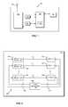
- FIG. 1illustrates an example of a simplified block diagram of part of an electronic device.
- FIG. 2illustrates an example of a part of an integrated circuit device comprising a clock signal generator module.
- FIG. 3illustrates an alternative example of a clock signal generator module.
- FIG. 4illustrates an alternative example of a clock signal generator module.
- FIG. 5illustrates an alternative example of a clock signal generator module.
- FIG. 6illustrates a simplified flowchart of an example of a method of generating at least one clock signal for at least one functional module.
- FIG. 7illustrates a simplified flowchart of an alternative example of a method of generating at least one clock signal for at least one functional module.
- the wireless communication unit 100is a mobile telephone handset comprising an antenna 102 .
- the wireless communication unit 100contains a variety of well known radio frequency (RF) components or circuits 106 , operably coupled to the antenna 102 , which for clarity reasons only will not be described further herein.
- the wireless communication unit 100further comprises signal processing logic 108 .
- An output from the signal processing logic 108is connected to a suitable user interface (UI) 110 comprising, for example, a display, keypad, microphone, speaker, etc., to input/output signals in a human perceptible form from/to a user.
- UIuser interface
- the signal processing logic 108is coupled to a memory element 116 that stores operating regimes, such as decoding/encoding functions and the like and may be realised in a variety of technologies, such as: random access memory (RAM)(volatile), (non-volatile) read only memory (ROM), Flash memory or any combination of these or other memory technologies.
- a timer 118may be coupled to the signal processing logic 108 in order to control a timing of operations within the communication unit 100 .
- FIG. 2there is illustrated a simplified block diagram of an example of part of an integrated circuit device 200 , such as may be implemented within, say, the radio frequency components or circuits 106 and/or the signal processing logic 108 of the wireless communication unit 100 of FIG. 1 .
- the integrated circuit device 200 of FIG. 2comprises a clock signal generator module 205 arranged to generate clock signals 210 , 212 , 214 for a plurality of functional modules 220 , 222 , 224 .
- the functional modules 220 , 222 , 224may comprise asynchronously clocked functional blocks.
- the clock signal generator module 205comprises clock source components 230 , 232 , 234 , each clock source component 230 , 232 , 234 being associated with one of the functional modules 220 , 222 , 224 and arranged to generate the respective clock signals, 210 , 212 , 214 .
- the clock source components 230 , 232 , 234comprise clock oscillators, more specific in this example ring oscillators.
- the clock signal generator module 205further comprises a management unit 240 arranged to controllably enable signal generation by the clock source components 230 , 232 , 234 in accordance with at least one operating characteristic of their respective functional module 220 , 222 , 224 associated therewith.
- the management unit 240may be arranged to controllably enable signal generation by the individual clock source components 230 , 232 , 234 based on periods of operation of the respective functional modules 220 , 222 , 224 associated therewith.
- the management unit 240may comprise, or form a part of, a power management unit for the clock source components 230 , 232 , 234 , and may be arranged to power up and power down the individual clock source components 230 , 232 , 234 to substantially match the periods of operation of the respective functional modules 220 , 222 , 224 associated therewith.
- the management unit 240may be operably coupled to each of the clock source components 230 , 232 , 234 via control signals 242 , via which the management unit 240 is able to power up/power down the individual clock source components 230 , 232 , 234 .
- the management unit 240may also comprise, or form a part of, a power management unit for the functional modules 220 , 222 , 224 , and thus may be arranged to power up and power down the individual clock source components 230 , 232 , 234 substantially concurrently with the respective functional modules 220 , 222 , 224 associated therewith. Accordingly, the management unit 240 may also be operably coupled to each of the functional modules 220 , 222 , 224 via control signals 244 , via which the management unit 240 is able to power up/down the individual functional modules 220 , 222 , 224 .
- each of the clock source components 230 , 232 , 234may be controlled such that it comprises operational periods that substantially match those of the respective functional module 220 , 222 , 224 associated therewith.
- ageing of the clock source components 230 , 232 , 234say due to the presence of voltage on their transistor gates (Negative Bias Temperature Instability), may be substantially matched to that of the respective functional module 220 , 222 , 224 associated therewith.
- the performance of the clock source components 230 , 232 , 234may be arranged to degrade through NBTI at substantially the same rate as that of the respective functional module 220 , 222 , 224 associated therewith.
- the potential performance of the respective functional module 220 , 222 , 224 reliant thereonmay be remain substantially fully utilized.
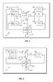
- FIG. 3there is illustrated a simplified block diagram of an example of an alternative clock signal generator module 305 arranged to generate a single clock signal 315 for a plurality of functional modules 220 , 222 , 224 .
- the functional modules 220 , 222 , 224may comprise synchronously clocked functional blocks, such as processing cores as illustrated in FIG. 3 .
- the clock signal generator module 305comprises clock source components 230 , 232 , 234 , each clock source component 230 , 232 , 234 being associated with one or more of the functional modules 220 , 222 , 224 and arranged to generate respective signals, 310 , 312 , 314 .
- a first clock source component 230may be associated with at least one functional module 220
- at least one further clock source 232 , 234may be associated with at least one further functional module 222 , 224 .
- the clock generator module 305further comprises a management unit 240 arranged to controllably enable signal generation by the clock source components 230 , 232 , 234 in accordance with at least one operating characteristic of the respective functional module(s) 220 , 222 , 224 associated therewith.
- the management unit 240may be arranged to controllably enable signal generation by the individual clock source components 230 , 232 , 234 based on periods of operation of the respective functional modules 220 , 222 , 224 associated therewith, such as described above in relation to the clock signal generator module 205 of FIG. 2 .
- each of the clock source components 230 , 232 , 234may be controlled such that it comprises operational periods that substantially match those of the respective functional module 220 , 222 , 224 associated therewith.
- ageing of the clock source components 230 , 232 , 234for example due to the presence of voltage on their transistor gates (Negative Bias Temperature Instability) may be substantially matched to that of the respective functional module 220 , 222 , 224 associated therewith.
- the performance of the clock source components 230 , 232 , 234may be arranged to degrade through NBTI at substantially the same rate as that of the respective functional module 220 , 222 , 224 associated therewith.
- the clock signal generator module 305is arranged to selectively output a clock signal 315 comprising one of the signals 310 , 312 , 314 output by the clock source components 230 , 232 , 234 .
- the clock signal generator module 305is arranged to selectively output a clock signal 315 comprising the signal 310 , 312 , 314 output by one of the clock source components 230 , 232 , 234 associated with an active functional module (e.g. a functional module currently powered up) comprising a highest power up/power down ratio.
- the functional modulecomprising the highest power up/power down ratio (e.g.
- the clock signal generator module 305comprises a multiplexer 350 arranged to receive at data inputs thereof the signals 310 , 312 , 314 output by the clock source components 230 , 232 , 234 , and to selectively output as the clock signal 315 one of the received signals 310 , 312 , 314 in accordance with a control signal 340 received from the at least one management unit 240 .
- the management unit 240may be arranged to store, for example within memory element 345 , statistical data relating to power up/down ratios for the functional modules 220 , 222 , 224 , and to determine which of the active functional modules 220 , 222 , 224 comprises the highest power up/down down ratio based on such statistical data.
- the clock signal 315 output by the clock signal generator module 305may comprise a signal generated by a clock source component 230 , 232 , 234 for which ageing has been arranged to substantially match that of the active functional module with the highest power up/power down ratio.
- performance of the active functional modules 220 , 222 , 224may be substantially optimized in accordance with the active functional module comprising the highest power up/down ratio.
- FIG. 4there is illustrated a simplified block diagram of an example of an alternative clock signal generator module 405 arranged to generate a single clock signal 415 for a one or more functional module(s) 420 .
- the clock signal generator module 405comprises clock source components 430 , 432 , each clock source component 430 , 432 being associated with the one or more functional module(s) 420 and arranged to generate respective clock signals 410 , 412 .
- the clock signal generator module 405further comprises a management unit 240 arranged to controllably enable signal generation by the clock source components 430 , 432 in accordance with switching activity for the functional module 420 associated therewith.
- the management unit 240may be arranged to cyclically enable signal generation of the clock source components 430 , 432 to substantially match switching activity for the functional module 420 associated therewith. For example, where switching activity for the functional module comprises, say, 60% of the clock signal provided thereto, the management unit 240 may be arranged to cyclically enable signal generation of the clock source components 430 , 432 such that signal generation for each of the clock source components 430 , 432 is enabled for 60% of the time. In this manner, ageing of the clock source components 430 , 432 due to switching activity (e.g. HCl) may be substantially matched to that of the functional module 420 associated therewith. Accordingly, the performance of the clock source components 430 , 432 may be arranged to degrade through HCl at substantially the same rate as that of the functional module 420 associated therewith.
- switching activity for the functional modulecomprises, say, 60% of the clock signal provided thereto
- the management unit 240may be arranged to cyclically enable signal generation of the clock source components 430
- the management unit 240may be arranged to cyclically enable signal generation of the clock source components 430 , 432 such that the periods of time in which the respective clock source components 430 , 432 are disabled are offset, and the clock signal generator module 405 may be arranged to output a clock signal 415 comprising interleaved signals 410 , 412 output by the clock source components 430 , 432 .
- the clock signal generator module 405comprises a multiplexer 450 arranged to receive at data inputs thereof the signals 410 , 412 output by the clock source components 430 , 432 , and to selectively output as the clock signal 415 one of the received signals 410 , 412 in accordance with a control signal 440 received from the management unit 240 .
- the management unit 240may be arranged to controllably enable signal generation by the clock source components 430 , 432 based at least partly on a pre-configured switching ratio for the functional module associated therewith. For example, such a pre-configured switching ratio may be determined based on test data or the like, and stored within memory element 345 . Additionally and/or alternatively the management unit 240 may be arranged to controllable enable signal generation by the clock source components 430 , 432 based at least partly on a derived switching ratio for the respective functional module 420 associated therewith.
- a switching ratio for the functional module 420may be derived at least partly from, say, statistical data obtained for clock gating functionality of the functional module 420 ; for example such clock gating functionality also being managed and/or controlled by the management unit 240 .
- FIG. 5there is illustrated a simplified block diagram of an example of an alternative clock signal generator module 505 arranged to generate a clock signal 515 for a plurality of functional modules 520 , 522 .
- the clock signal generator module 505comprises clock source components 530 , 532 , 534 , 536 ; each clock source component 530 , 532 , 534 , 536 being associated with at least one of the functional modules 520 , 522 , and arranged to generate respective signals 510 , 512 , 514 , 516 .
- FIG. 5the example illustrated in FIG.
- the clock source components 530 , 532 , 534 , 536are arranged into groups 550 , 555 , each group 550 , 555 being associated with a functional module 520 , 522 and comprising, in the illustrated example, a pair of clock source components 530 , 532 and 534 , 536 respectively.
- the clock signal generator module 505further comprises a management unit 240 arranged to controllably enable signal generation by the clock source components 530 , 532 , 534 , 536 in accordance with periods of operation of the respective functional module(s) 520 , 522 associated therewith, as well as in accordance with switching activity for the functional module(s) 520 , 522 associated therewith.
- a management unit 240arranged to controllably enable signal generation by the clock source components 530 , 532 , 534 , 536 in accordance with periods of operation of the respective functional module(s) 520 , 522 associated therewith, as well as in accordance with switching activity for the functional module(s) 520 , 522 associated therewith.
- the management unit 240may be arranged to controllably enable signal generation by individual groups 550 , 555 of clock source components 530 , 532 , 534 , 536 based on periods of operation of the respective functional modules 520 , 522 associated therewith.
- each group 550 , 555 of clock source components 530 , 532 , 534 , 536may be controlled such that the clock source components 530 , 532 , 534 , 536 therein comprise operational periods that substantially match those of the respective functional module 520 , 522 associated therewith.
- ageing of the clock source components 530 , 532 , 534 , 536 due to the presence of voltage on their transistor gates (e.g. NBTI)may be substantially matched to that of the respective functional module 520 , 522 associated therewith.
- the management module 240may further be arranged to controllably enable signal generation by the clock source components 530 , 532 , 534 , 536 in accordance with switching activity for the functional module(s) 520 , 522 associated therewith.
- the management unit 240may be arranged to cyclically enable signal generation of the clock source components 530 , 532 , 534 , 536 to substantially match switching activity for the functional modules 520 , 522 associated therewith. In this manner, ageing of the clock source components 530 , 532 , 534 , 536 due to switching activity (e.g. HCl) may also be substantially matched to that of the functional modules 520 , 522 associated therewith.
- switching activitye.g. HCl
- FIGS. 2 to 5For clarity and ease of understanding, alternative example arrangements have been illustrated separately within FIGS. 2 to 5 . However, it will be appreciated that such arrangements are not limited to being implemented in isolation, and any combination of such arrangements may be equally implemented.
- the arrangement illustrated in FIG. 2 for asynchronously clocked functional blocksmay be implemented in combination with, say, one of the arrangements illustrated in FIGS. 3 to 5 for synchronously clocked functional blocks.
- FIG. 6there is illustrated a simplified flowchart 600 of an example of a method of generating a clock signal for at least one functional module.
- the methodstarts at 610 , and moves on to 620 where, in the illustrated example, power supplies for clock source components (e.g. ring oscillators) are configured (e.g. to power up or power down) to substantially match power supplies of functional modules associated with the respective clock source components. In this manner, signal generation by each clock source component may be enabled based at least partly on periods of operation of the respective functional module(s) associated therewith.
- an active functional modulecomprising a highest power up/power down ratio is determined.
- a clock signalis then output comprising a signal output by a clock source component associated with the determined active functional module comprising the highest power up/power down ratio, at 640 .
- the methodends at 650 .
- FIG. 7there is illustrated a simplified flowchart 700 of an alternative example of a method of generating a clock signal for at least one functional module.
- the methodstarts at 710 , and moves on to 720 where a switching activity ratio is determined for at least one functional module.
- power cycling of clock source components associated with the at least one functional moduleis configured to substantially match the determined switching activity ratio of the at least one functional module associated therewith.
- Interleaving of signals output by the clock source componentsis then configured to generate a substantially continuous clock signal, at 740 , and the method ends at 750 .
- FIGS. 6 and 7For clarity and ease of understanding, alternative example methods have been illustrated separately within FIGS. 6 and 7 . However, it will be appreciated that such methods are not limited to being implemented in isolation, and such methods may be equally implemented in combination. For example, the method illustrated in FIG. 7 may be implemented in, say, 640 of the method illustrated in FIG. 6 .
- connections as discussed hereinmay be any type of connection suitable to transfer signals from or to the respective nodes, units or devices, for example via intermediate devices. Accordingly, unless implied or stated otherwise, the connections may for example be direct connections or indirect connections.
- the connectionsmay be illustrated or described in reference to being a single connection, a plurality of connections, unidirectional connections, or bidirectional connections. However, different embodiments may vary the implementation of the connections. For example, separate unidirectional connections may be used rather than bidirectional connections and vice versa.
- plurality of connectionsmay be replaced with a single connection that transfers multiple signals serially or in a time multiplexed manner. Likewise, single connections carrying multiple signals may be separated out into various different connections carrying subsets of these signals. Therefore, many options exist for transferring signals.
- Each signal described hereinmay be designed as positive or negative logic.
- the signalIn the case of a negative logic signal, the signal is active low where the logically true state corresponds to a logic level zero.
- the signalIn the case of a positive logic signal, the signal is active high where the logically true state corresponds to a logic level one.
- any of the signals described hereincan be designed as either negative or positive logic signals. Therefore, in alternate embodiments, those signals described as positive logic signals may be implemented as negative logic signals, and those signals described as negative logic signals may be implemented as positive logic signals.
- logic blocksare merely illustrative and that alternative embodiments may merge logic blocks or circuit elements or impose an alternate decomposition of functionality upon various logic blocks or circuit elements.
- architectures depicted hereinare merely exemplary, and that in fact many other architectures can be implemented which achieve the same functionality.
- any arrangement of components to achieve the same functionalityis effectively ‘associated’ such that the desired functionality is achieved.
- any two components herein combined to achieve a particular functionalitycan be seen as ‘associated with’ each other such that the desired functionality is achieved, irrespective of architectures or intermediary components.
- any two components so associatedcan also be viewed as being ‘operably connected’, or ‘operably coupled’, to each other to achieve the desired functionality.
- the examples, or portions thereofmay implemented as soft or code representations of physical circuitry or of logical representations convertible into physical circuitry, such as in a hardware description language of any appropriate type.
- the inventionis not limited to physical devices or units implemented in non-programmable hardware but can also be applied in programmable devices or units able to perform the desired device functions by operating in accordance with suitable program code, such as mainframes, minicomputers, servers, workstations, personal computers, notepads, personal digital assistants, electronic games, automotive and other embedded systems, cell phones and various other wireless devices, commonly denoted in this application as ‘computer systems’.
- suitable program codesuch as mainframes, minicomputers, servers, workstations, personal computers, notepads, personal digital assistants, electronic games, automotive and other embedded systems, cell phones and various other wireless devices, commonly denoted in this application as ‘computer systems’.
- any reference signs placed between parenthesesshall not be construed as limiting the claim.
- the word ‘comprising’does not exclude the presence of other elements or steps then those listed in a claim.
- the terms ‘a’ or ‘an,’ as used hereinare defined as one or more than one.
- the use of introductory phrases such as ‘at least one’ and ‘one or more’ in the claimsshould not be construed to imply that the introduction of another claim element by the indefinite articles ‘a’ or ‘an’ limits any particular claim containing such introduced claim element to inventions containing only one such element, even when the same claim includes the introductory phrases ‘one or more’ or ‘at least one’ and indefinite articles such as ‘a’ or ‘an’.
Landscapes
- Physics & Mathematics (AREA)
- Engineering & Computer Science (AREA)
- Computer Hardware Design (AREA)
- Nonlinear Science (AREA)
- Computing Systems (AREA)
- General Engineering & Computer Science (AREA)
- Mathematical Physics (AREA)
- Semiconductor Integrated Circuits (AREA)
Abstract
Description
Claims (20)
Applications Claiming Priority (1)
| Application Number | Priority Date | Filing Date | Title |
|---|---|---|---|
| PCT/IB2011/055213WO2013076524A1 (en) | 2011-11-21 | 2011-11-21 | Clock signal generator module, integrated circuit, electronic device and method therefore |
Publications (2)
| Publication Number | Publication Date |
|---|---|
| US20140253204A1 US20140253204A1 (en) | 2014-09-11 |
| US9093989B2true US9093989B2 (en) | 2015-07-28 |
Family
ID=48469207
Family Applications (1)
| Application Number | Title | Priority Date | Filing Date |
|---|---|---|---|
| US14/352,706ActiveUS9093989B2 (en) | 2011-11-21 | 2011-11-21 | Clock signal generator module, integrated circuit, electronic device and method therefor |
Country Status (2)
| Country | Link |
|---|---|
| US (1) | US9093989B2 (en) |
| WO (1) | WO2013076524A1 (en) |
Families Citing this family (2)
| Publication number | Priority date | Publication date | Assignee | Title |
|---|---|---|---|---|
| US9118310B1 (en)* | 2014-09-10 | 2015-08-25 | Xilinx, Inc. | Programmable delay circuit block |
| KR20180033960A (en) | 2016-09-27 | 2018-04-04 | 삼성전자주식회사 | Clock switch device and system-on-chip having the same |
Citations (7)
| Publication number | Priority date | Publication date | Assignee | Title |
|---|---|---|---|---|
| US20060218428A1 (en) | 2005-03-22 | 2006-09-28 | Hurd Kevin A | Systems and methods for operating within operating condition limits |
| US20070152739A1 (en) | 2006-01-03 | 2007-07-05 | Freescale Semiconductor, Inc. | Power management in integrated circuits using process detection |
| US20080120065A1 (en) | 2006-11-17 | 2008-05-22 | Mayur Joshi | Accurate Integrated Circuit Performance Prediction Using On-Board Sensors |
| US20080252329A1 (en) | 2003-12-31 | 2008-10-16 | Ravisangar Muniandy | On-chip frequency degradation compensation |
| US20100194400A1 (en) | 2009-02-02 | 2010-08-05 | Thomas Baumann | Circuit Arrangement With A Test Circuit And A Reference Circuit And Corresponding Method |
| US7772910B2 (en)* | 2007-03-14 | 2010-08-10 | Samsung Electronics Co., Ltd. | Internal clock generator, system and method |
| US8013635B2 (en) | 2010-02-11 | 2011-09-06 | Texas Instruments Incorporated | Multi-mode circuit and a method for preventing degradation in the multi-mode circuit |
- 2011
- 2011-11-21USUS14/352,706patent/US9093989B2/enactiveActive
- 2011-11-21WOPCT/IB2011/055213patent/WO2013076524A1/enactiveApplication Filing
Patent Citations (7)
| Publication number | Priority date | Publication date | Assignee | Title |
|---|---|---|---|---|
| US20080252329A1 (en) | 2003-12-31 | 2008-10-16 | Ravisangar Muniandy | On-chip frequency degradation compensation |
| US20060218428A1 (en) | 2005-03-22 | 2006-09-28 | Hurd Kevin A | Systems and methods for operating within operating condition limits |
| US20070152739A1 (en) | 2006-01-03 | 2007-07-05 | Freescale Semiconductor, Inc. | Power management in integrated circuits using process detection |
| US20080120065A1 (en) | 2006-11-17 | 2008-05-22 | Mayur Joshi | Accurate Integrated Circuit Performance Prediction Using On-Board Sensors |
| US7772910B2 (en)* | 2007-03-14 | 2010-08-10 | Samsung Electronics Co., Ltd. | Internal clock generator, system and method |
| US20100194400A1 (en) | 2009-02-02 | 2010-08-05 | Thomas Baumann | Circuit Arrangement With A Test Circuit And A Reference Circuit And Corresponding Method |
| US8013635B2 (en) | 2010-02-11 | 2011-09-06 | Texas Instruments Incorporated | Multi-mode circuit and a method for preventing degradation in the multi-mode circuit |
Non-Patent Citations (1)
| Title |
|---|
| International Search Report and Written Opinion correlating to PCT/IB2011/055213 dated Jul. 30, 2012. |
Also Published As
| Publication number | Publication date |
|---|---|
| US20140253204A1 (en) | 2014-09-11 |
| WO2013076524A1 (en) | 2013-05-30 |
Similar Documents
| Publication | Publication Date | Title |
|---|---|---|
| US9753486B2 (en) | Clock gating with an asynchronous wrapper cell | |
| US20130015904A1 (en) | Power gating control module, integrated circuit device, signal processing system, electronic device, and method therefor | |
| US8456140B2 (en) | Power control apparatus and method for controlling a supply voltage for an associated circuit | |
| US9246489B1 (en) | Integrated clock gating cell using a low area and a low power latch | |
| US6784699B2 (en) | Glitch free clock multiplexing circuit with asynchronous switch control and minimum switch over time | |
| US7737740B2 (en) | Integrated circuit with a programmable delay and a method thereof | |
| US9553567B2 (en) | Fast settling charge pump with frequency hopping | |
| US7215155B2 (en) | Control circuits and methods including delay times for multi-threshold CMOS devices | |
| US10491217B2 (en) | Low-power clock gate circuit | |
| US20160132070A1 (en) | Oscillator circuit and method of generating a clock signal | |
| JP5462703B2 (en) | Leakage current reduction system in sequential circuit | |
| Kong et al. | Fast scaling in the residue number system | |
| WO2012131425A1 (en) | Integrated circuit and method for reducing an impact of electrical stress in an integrated circuit | |
| US8692602B2 (en) | Method and apparatus of digital control delay line | |
| US9093989B2 (en) | Clock signal generator module, integrated circuit, electronic device and method therefor | |
| US9442463B2 (en) | Time-to-digital converter (TDC) with offset cancellation | |
| US10418975B2 (en) | Low clock supply voltage interruptible sequential | |
| EP2965424A1 (en) | Low leakage retention register tray | |
| US20230388100A1 (en) | Reference Clock Switching in Phase-Locked Loop Circuits | |
| WO2011107828A1 (en) | Integrated circuit device comprising clock gating circuitry, electronic device and method for dynamically configuring clock gating | |
| US9178730B2 (en) | Clock distribution module, synchronous digital system and method therefor | |
| CN101911487B (en) | System and method of conditional control of latch circuit devices | |
| EP3574584A1 (en) | Variable delay circuits | |
| CN118074680B (en) | A delay chain circuit with configurable delay time | |
| US9462556B2 (en) | Integrated circuit device, signal processing system, electronic device and method for configuring a signal processing operating mode |
Legal Events
| Date | Code | Title | Description |
|---|---|---|---|
| AS | Assignment | Owner name:FREESCALE SEMICONDUCTOR INC., TEXAS Free format text:ASSIGNMENT OF ASSIGNORS INTEREST;ASSIGNORS:ROZEN, ANTON;PRIEL, MICHAEL;SHOSHANY, YOSSI;REEL/FRAME:032705/0956 Effective date:20111128 | |
| AS | Assignment | Owner name:CITIBANK, N.A., AS NOTES COLLATERAL AGENT, NEW YORK Free format text:SUPPLEMENT TO IP SECURITY AGREEMENT;ASSIGNOR:FREESCALE SEMICONDUCTOR, INC.;REEL/FRAME:033460/0337 Effective date:20140729 Owner name:CITIBANK, N.A., AS NOTES COLLATERAL AGENT, NEW YORK Free format text:SUPPLEMENT TO IP SECURITY AGREEMENT;ASSIGNOR:FREESCALE SEMICONDUCTOR, INC.;REEL/FRAME:033462/0267 Effective date:20140729 Owner name:CITIBANK, N.A., AS NOTES COLLATERAL AGENT, NEW YORK Free format text:SUPPLEMENT TO IP SECURITY AGREEMENT;ASSIGNOR:FREESCALE SEMICONDUCTOR, INC.;REEL/FRAME:033462/0293 Effective date:20140729 Owner name:CITIBANK, N.A., AS NOTES COLLATERAL AGENT, NEW YOR Free format text:SUPPLEMENT TO IP SECURITY AGREEMENT;ASSIGNOR:FREESCALE SEMICONDUCTOR, INC.;REEL/FRAME:033460/0337 Effective date:20140729 Owner name:CITIBANK, N.A., AS NOTES COLLATERAL AGENT, NEW YOR Free format text:SUPPLEMENT TO IP SECURITY AGREEMENT;ASSIGNOR:FREESCALE SEMICONDUCTOR, INC.;REEL/FRAME:033462/0267 Effective date:20140729 Owner name:CITIBANK, N.A., AS NOTES COLLATERAL AGENT, NEW YOR Free format text:SUPPLEMENT TO IP SECURITY AGREEMENT;ASSIGNOR:FREESCALE SEMICONDUCTOR, INC.;REEL/FRAME:033462/0293 Effective date:20140729 | |
| STCF | Information on status: patent grant | Free format text:PATENTED CASE | |
| AS | Assignment | Owner name:FREESCALE SEMICONDUCTOR, INC., TEXAS Free format text:PATENT RELEASE;ASSIGNOR:CITIBANK, N.A., AS COLLATERAL AGENT;REEL/FRAME:037357/0903 Effective date:20151207 | |
| AS | Assignment | Owner name:MORGAN STANLEY SENIOR FUNDING, INC., MARYLAND Free format text:ASSIGNMENT AND ASSUMPTION OF SECURITY INTEREST IN PATENTS;ASSIGNOR:CITIBANK, N.A.;REEL/FRAME:037444/0082 Effective date:20151207 Owner name:MORGAN STANLEY SENIOR FUNDING, INC., MARYLAND Free format text:ASSIGNMENT AND ASSUMPTION OF SECURITY INTEREST IN PATENTS;ASSIGNOR:CITIBANK, N.A.;REEL/FRAME:037444/0109 Effective date:20151207 | |
| AS | Assignment | Owner name:MORGAN STANLEY SENIOR FUNDING, INC., MARYLAND Free format text:SECURITY AGREEMENT SUPPLEMENT;ASSIGNOR:NXP B.V.;REEL/FRAME:038017/0058 Effective date:20160218 | |
| AS | Assignment | Owner name:MORGAN STANLEY SENIOR FUNDING, INC., MARYLAND Free format text:SUPPLEMENT TO THE SECURITY AGREEMENT;ASSIGNOR:FREESCALE SEMICONDUCTOR, INC.;REEL/FRAME:039138/0001 Effective date:20160525 | |
| AS | Assignment | Owner name:MORGAN STANLEY SENIOR FUNDING, INC., MARYLAND Free format text:CORRECTIVE ASSIGNMENT TO CORRECT THE REMOVE APPLICATION 12092129 PREVIOUSLY RECORDED ON REEL 038017 FRAME 0058. ASSIGNOR(S) HEREBY CONFIRMS THE SECURITY AGREEMENT SUPPLEMENT;ASSIGNOR:NXP B.V.;REEL/FRAME:039361/0212 Effective date:20160218 | |
| AS | Assignment | Owner name:MORGAN STANLEY SENIOR FUNDING, INC., MARYLAND Free format text:CORRECTIVE ASSIGNMENT TO CORRECT THE REMOVE APPLICATION 14/258,829 AND REPLACE ITWITH 14/258,629 PREVIOUSLY RECORDED ON REEL 037444 FRAME 0082. ASSIGNOR(S) HEREBY CONFIRMS THE ASSIGNMENT AND ASSUMPTION OFSECURITY INTEREST IN PATENTS;ASSIGNOR:CITIBANK, N.A.;REEL/FRAME:039639/0332 Effective date:20151207 Owner name:MORGAN STANLEY SENIOR FUNDING, INC., MARYLAND Free format text:CORRECTIVE ASSIGNMENT TO CORRECT THE REMOVE APPLICATION14/258,829 AND REPLACE IT WITH 14/258,629 PREVIOUSLY RECORDED ON REEL 037444 FRAME 0109. ASSIGNOR(S) HEREBY CONFIRMS THE ASSIGNMENT AND ASSUMPTION OF SECURITY INTEREST IN PATENTS;ASSIGNOR:CITIBANK, N.A.;REEL/FRAME:039639/0208 Effective date:20151207 Owner name:MORGAN STANLEY SENIOR FUNDING, INC., MARYLAND Free format text:CORRECTIVE ASSIGNMENT OF INCORRECT APPLICATION 14/258,829 PREVIOUSLY RECORDED ON REEL 037444 FRAME 0109. ASSIGNOR(S) HEREBY CONFIRMS THE ASSIGNMENT AND ASSUMPTION OF SECURITY INTEREST IN PATENTS;ASSIGNOR:CITIBANK, N.A.;REEL/FRAME:039639/0208 Effective date:20151207 | |
| AS | Assignment | Owner name:NXP, B.V., F/K/A FREESCALE SEMICONDUCTOR, INC., NETHERLANDS Free format text:RELEASE BY SECURED PARTY;ASSIGNOR:MORGAN STANLEY SENIOR FUNDING, INC.;REEL/FRAME:040925/0001 Effective date:20160912 Owner name:NXP, B.V., F/K/A FREESCALE SEMICONDUCTOR, INC., NE Free format text:RELEASE BY SECURED PARTY;ASSIGNOR:MORGAN STANLEY SENIOR FUNDING, INC.;REEL/FRAME:040925/0001 Effective date:20160912 | |
| AS | Assignment | Owner name:NXP B.V., NETHERLANDS Free format text:RELEASE BY SECURED PARTY;ASSIGNOR:MORGAN STANLEY SENIOR FUNDING, INC.;REEL/FRAME:040928/0001 Effective date:20160622 | |
| AS | Assignment | Owner name:NXP USA, INC., TEXAS Free format text:CHANGE OF NAME;ASSIGNOR:FREESCALE SEMICONDUCTOR, INC.;REEL/FRAME:040652/0241 Effective date:20161107 Owner name:NXP USA, INC., TEXAS Free format text:MERGER;ASSIGNOR:FREESCALE SEMICONDUCTOR, INC.;REEL/FRAME:040652/0241 Effective date:20161107 | |
| AS | Assignment | Owner name:NXP USA, INC., TEXAS Free format text:CORRECTIVE ASSIGNMENT TO CORRECT THE NATURE OF CONVEYANCE PREVIOUSLY RECORDED AT REEL: 040652 FRAME: 0241. ASSIGNOR(S) HEREBY CONFIRMS THE MERGER AND CHANGE OF NAME;ASSIGNOR:FREESCALE SEMICONDUCTOR, INC.;REEL/FRAME:041260/0850 Effective date:20161107 | |
| AS | Assignment | Owner name:MORGAN STANLEY SENIOR FUNDING, INC., MARYLAND Free format text:CORRECTIVE ASSIGNMENT TO CORRECT THE REMOVE APPLICATION 12681366 PREVIOUSLY RECORDED ON REEL 039361 FRAME 0212. ASSIGNOR(S) HEREBY CONFIRMS THE SECURITY AGREEMENT SUPPLEMENT;ASSIGNOR:NXP B.V.;REEL/FRAME:042762/0145 Effective date:20160218 Owner name:MORGAN STANLEY SENIOR FUNDING, INC., MARYLAND Free format text:CORRECTIVE ASSIGNMENT TO CORRECT THE REMOVE APPLICATION 12681366 PREVIOUSLY RECORDED ON REEL 038017 FRAME 0058. ASSIGNOR(S) HEREBY CONFIRMS THE SECURITY AGREEMENT SUPPLEMENT;ASSIGNOR:NXP B.V.;REEL/FRAME:042985/0001 Effective date:20160218 | |
| MAFP | Maintenance fee payment | Free format text:PAYMENT OF MAINTENANCE FEE, 4TH YEAR, LARGE ENTITY (ORIGINAL EVENT CODE: M1551); ENTITY STATUS OF PATENT OWNER: LARGE ENTITY Year of fee payment:4 | |
| AS | Assignment | Owner name:NXP B.V., NETHERLANDS Free format text:RELEASE BY SECURED PARTY;ASSIGNOR:MORGAN STANLEY SENIOR FUNDING, INC.;REEL/FRAME:050745/0001 Effective date:20190903 Owner name:NXP B.V., NETHERLANDS Free format text:RELEASE BY SECURED PARTY;ASSIGNOR:MORGAN STANLEY SENIOR FUNDING, INC.;REEL/FRAME:050744/0097 Effective date:20190903 | |
| AS | Assignment | Owner name:MORGAN STANLEY SENIOR FUNDING, INC., MARYLAND Free format text:CORRECTIVE ASSIGNMENT TO CORRECT THE REMOVE APPLICATION 12298143 PREVIOUSLY RECORDED ON REEL 042762 FRAME 0145. ASSIGNOR(S) HEREBY CONFIRMS THE SECURITY AGREEMENT SUPPLEMENT;ASSIGNOR:NXP B.V.;REEL/FRAME:051145/0184 Effective date:20160218 Owner name:MORGAN STANLEY SENIOR FUNDING, INC., MARYLAND Free format text:CORRECTIVE ASSIGNMENT TO CORRECT THE REMOVE APPLICATION 12298143 PREVIOUSLY RECORDED ON REEL 039361 FRAME 0212. ASSIGNOR(S) HEREBY CONFIRMS THE SECURITY AGREEMENT SUPPLEMENT;ASSIGNOR:NXP B.V.;REEL/FRAME:051029/0387 Effective date:20160218 Owner name:MORGAN STANLEY SENIOR FUNDING, INC., MARYLAND Free format text:CORRECTIVE ASSIGNMENT TO CORRECT THE REMOVE APPLICATION 12298143 PREVIOUSLY RECORDED ON REEL 042985 FRAME 0001. ASSIGNOR(S) HEREBY CONFIRMS THE SECURITY AGREEMENT SUPPLEMENT;ASSIGNOR:NXP B.V.;REEL/FRAME:051029/0001 Effective date:20160218 Owner name:MORGAN STANLEY SENIOR FUNDING, INC., MARYLAND Free format text:CORRECTIVE ASSIGNMENT TO CORRECT THE REMOVE APPLICATION 12298143 PREVIOUSLY RECORDED ON REEL 038017 FRAME 0058. ASSIGNOR(S) HEREBY CONFIRMS THE SECURITY AGREEMENT SUPPLEMENT;ASSIGNOR:NXP B.V.;REEL/FRAME:051030/0001 Effective date:20160218 Owner name:MORGAN STANLEY SENIOR FUNDING, INC., MARYLAND Free format text:CORRECTIVE ASSIGNMENT TO CORRECT THE REMOVE APPLICATION12298143 PREVIOUSLY RECORDED ON REEL 039361 FRAME 0212. ASSIGNOR(S) HEREBY CONFIRMS THE SECURITY AGREEMENT SUPPLEMENT;ASSIGNOR:NXP B.V.;REEL/FRAME:051029/0387 Effective date:20160218 Owner name:MORGAN STANLEY SENIOR FUNDING, INC., MARYLAND Free format text:CORRECTIVE ASSIGNMENT TO CORRECT THE REMOVE APPLICATION12298143 PREVIOUSLY RECORDED ON REEL 042985 FRAME 0001. ASSIGNOR(S) HEREBY CONFIRMS THE SECURITY AGREEMENT SUPPLEMENT;ASSIGNOR:NXP B.V.;REEL/FRAME:051029/0001 Effective date:20160218 Owner name:MORGAN STANLEY SENIOR FUNDING, INC., MARYLAND Free format text:CORRECTIVE ASSIGNMENT TO CORRECT THE REMOVE APPLICATION12298143 PREVIOUSLY RECORDED ON REEL 042762 FRAME 0145. ASSIGNOR(S) HEREBY CONFIRMS THE SECURITY AGREEMENT SUPPLEMENT;ASSIGNOR:NXP B.V.;REEL/FRAME:051145/0184 Effective date:20160218 | |
| AS | Assignment | Owner name:NXP B.V., NETHERLANDS Free format text:CORRECTIVE ASSIGNMENT TO CORRECT THE REMOVEAPPLICATION 11759915 AND REPLACE IT WITH APPLICATION11759935 PREVIOUSLY RECORDED ON REEL 040928 FRAME 0001. ASSIGNOR(S) HEREBY CONFIRMS THE RELEASE OF SECURITYINTEREST;ASSIGNOR:MORGAN STANLEY SENIOR FUNDING, INC.;REEL/FRAME:052915/0001 Effective date:20160622 | |
| AS | Assignment | Owner name:NXP, B.V. F/K/A FREESCALE SEMICONDUCTOR, INC., NETHERLANDS Free format text:CORRECTIVE ASSIGNMENT TO CORRECT THE REMOVEAPPLICATION 11759915 AND REPLACE IT WITH APPLICATION11759935 PREVIOUSLY RECORDED ON REEL 040925 FRAME 0001. ASSIGNOR(S) HEREBY CONFIRMS THE RELEASE OF SECURITYINTEREST;ASSIGNOR:MORGAN STANLEY SENIOR FUNDING, INC.;REEL/FRAME:052917/0001 Effective date:20160912 | |
| MAFP | Maintenance fee payment | Free format text:PAYMENT OF MAINTENANCE FEE, 8TH YEAR, LARGE ENTITY (ORIGINAL EVENT CODE: M1552); ENTITY STATUS OF PATENT OWNER: LARGE ENTITY Year of fee payment:8 |