US9093800B2 - Leadframe module for an electrical connector - Google Patents
Leadframe module for an electrical connectorDownload PDFInfo
- Publication number
- US9093800B2 US9093800B2US13/658,340US201213658340AUS9093800B2US 9093800 B2US9093800 B2US 9093800B2US 201213658340 AUS201213658340 AUS 201213658340AUS 9093800 B2US9093800 B2US 9093800B2
- Authority
- US
- United States
- Prior art keywords
- contacts
- leadframe
- outer shields
- dielectric shells
- dielectric
- Prior art date
- Legal status (The legal status is an assumption and is not a legal conclusion. Google has not performed a legal analysis and makes no representation as to the accuracy of the status listed.)
- Active, expires
Links
- 230000005540biological transmissionEffects0.000claimsabstractdescription60
- 230000013011matingEffects0.000claimsabstractdescription53
- 239000004020conductorSubstances0.000claimsabstractdescription10
- 238000000034methodMethods0.000claimsdescription28
- 238000000576coating methodMethods0.000claimsdescription24
- 239000011248coating agentSubstances0.000claimsdescription23
- 239000003989dielectric materialSubstances0.000claimsdescription16
- 230000007704transitionEffects0.000claimsdescription12
- 238000004519manufacturing processMethods0.000claimsdescription7
- 239000000843powderSubstances0.000claimsdescription6
- 238000007639printingMethods0.000claimsdescription5
- 230000008878couplingEffects0.000claimsdescription2
- 238000010168coupling processMethods0.000claimsdescription2
- 238000005859coupling reactionMethods0.000claimsdescription2
- 238000007747platingMethods0.000claimsdescription2
- 230000008569processEffects0.000description15
- 238000012805post-processingMethods0.000description10
- 229910052751metalInorganic materials0.000description6
- 239000002184metalSubstances0.000description6
- 239000000463materialSubstances0.000description4
- 238000012986modificationMethods0.000description3
- 230000004048modificationEffects0.000description3
- 238000005520cutting processMethods0.000description2
- 238000005507sprayingMethods0.000description2
- 239000000758substrateSubstances0.000description2
- BQCADISMDOOEFD-UHFFFAOYSA-NSilverChemical compound[Ag]BQCADISMDOOEFD-UHFFFAOYSA-N0.000description1
- 238000005229chemical vapour depositionMethods0.000description1
- 238000002788crimpingMethods0.000description1
- 238000007598dipping methodMethods0.000description1
- 238000007772electroless platingMethods0.000description1
- 238000009713electroplatingMethods0.000description1
- 239000011159matrix materialSubstances0.000description1
- 238000005240physical vapour depositionMethods0.000description1
- 238000004080punchingMethods0.000description1
- 238000000926separation methodMethods0.000description1
- 229910052709silverInorganic materials0.000description1
- 239000004332silverSubstances0.000description1
- 229910000679solderInorganic materials0.000description1
- 238000005476solderingMethods0.000description1
- 239000007921spraySubstances0.000description1
- 239000011800void materialSubstances0.000description1
Images


Classifications
- H—ELECTRICITY
- H01—ELECTRIC ELEMENTS
- H01R—ELECTRICALLY-CONDUCTIVE CONNECTIONS; STRUCTURAL ASSOCIATIONS OF A PLURALITY OF MUTUALLY-INSULATED ELECTRICAL CONNECTING ELEMENTS; COUPLING DEVICES; CURRENT COLLECTORS
- H01R12/00—Structural associations of a plurality of mutually-insulated electrical connecting elements, specially adapted for printed circuits, e.g. printed circuit boards [PCB], flat or ribbon cables, or like generally planar structures, e.g. terminal strips, terminal blocks; Coupling devices specially adapted for printed circuits, flat or ribbon cables, or like generally planar structures; Terminals specially adapted for contact with, or insertion into, printed circuits, flat or ribbon cables, or like generally planar structures
- H01R12/70—Coupling devices
- H01R12/71—Coupling devices for rigid printing circuits or like structures
- H01R12/72—Coupling devices for rigid printing circuits or like structures coupling with the edge of the rigid printed circuits or like structures
- H01R12/722—Coupling devices for rigid printing circuits or like structures coupling with the edge of the rigid printed circuits or like structures coupling devices mounted on the edge of the printed circuits
- H01R12/727—Coupling devices presenting arrays of contacts
- H—ELECTRICITY
- H01—ELECTRIC ELEMENTS
- H01R—ELECTRICALLY-CONDUCTIVE CONNECTIONS; STRUCTURAL ASSOCIATIONS OF A PLURALITY OF MUTUALLY-INSULATED ELECTRICAL CONNECTING ELEMENTS; COUPLING DEVICES; CURRENT COLLECTORS
- H01R12/00—Structural associations of a plurality of mutually-insulated electrical connecting elements, specially adapted for printed circuits, e.g. printed circuit boards [PCB], flat or ribbon cables, or like generally planar structures, e.g. terminal strips, terminal blocks; Coupling devices specially adapted for printed circuits, flat or ribbon cables, or like generally planar structures; Terminals specially adapted for contact with, or insertion into, printed circuits, flat or ribbon cables, or like generally planar structures
- H01R12/70—Coupling devices
- H01R12/71—Coupling devices for rigid printing circuits or like structures
- H01R12/72—Coupling devices for rigid printing circuits or like structures coupling with the edge of the rigid printed circuits or like structures
- H—ELECTRICITY
- H01—ELECTRIC ELEMENTS
- H01R—ELECTRICALLY-CONDUCTIVE CONNECTIONS; STRUCTURAL ASSOCIATIONS OF A PLURALITY OF MUTUALLY-INSULATED ELECTRICAL CONNECTING ELEMENTS; COUPLING DEVICES; CURRENT COLLECTORS
- H01R13/00—Details of coupling devices of the kinds covered by groups H01R12/70 or H01R24/00 - H01R33/00
- H01R13/02—Contact members
- H01R13/03—Contact members characterised by the material, e.g. plating, or coating materials
- H01R13/035—Plated dielectric material
- H—ELECTRICITY
- H01—ELECTRIC ELEMENTS
- H01R—ELECTRICALLY-CONDUCTIVE CONNECTIONS; STRUCTURAL ASSOCIATIONS OF A PLURALITY OF MUTUALLY-INSULATED ELECTRICAL CONNECTING ELEMENTS; COUPLING DEVICES; CURRENT COLLECTORS
- H01R13/00—Details of coupling devices of the kinds covered by groups H01R12/70 or H01R24/00 - H01R33/00
- H01R13/648—Protective earth or shield arrangements on coupling devices, e.g. anti-static shielding
- H01R13/658—High frequency shielding arrangements, e.g. against EMI [Electro-Magnetic Interference] or EMP [Electro-Magnetic Pulse]
- H01R13/6581—Shield structure
- H01R13/6585—Shielding material individually surrounding or interposed between mutually spaced contacts
- H—ELECTRICITY
- H01—ELECTRIC ELEMENTS
- H01R—ELECTRICALLY-CONDUCTIVE CONNECTIONS; STRUCTURAL ASSOCIATIONS OF A PLURALITY OF MUTUALLY-INSULATED ELECTRICAL CONNECTING ELEMENTS; COUPLING DEVICES; CURRENT COLLECTORS
- H01R12/00—Structural associations of a plurality of mutually-insulated electrical connecting elements, specially adapted for printed circuits, e.g. printed circuit boards [PCB], flat or ribbon cables, or like generally planar structures, e.g. terminal strips, terminal blocks; Coupling devices specially adapted for printed circuits, flat or ribbon cables, or like generally planar structures; Terminals specially adapted for contact with, or insertion into, printed circuits, flat or ribbon cables, or like generally planar structures
- H01R12/70—Coupling devices
- H01R12/71—Coupling devices for rigid printing circuits or like structures
- H01R12/72—Coupling devices for rigid printing circuits or like structures coupling with the edge of the rigid printed circuits or like structures
- H01R12/722—Coupling devices for rigid printing circuits or like structures coupling with the edge of the rigid printed circuits or like structures coupling devices mounted on the edge of the printed circuits
- H01R12/724—Coupling devices for rigid printing circuits or like structures coupling with the edge of the rigid printed circuits or like structures coupling devices mounted on the edge of the printed circuits containing contact members forming a right angle
- H—ELECTRICITY
- H01—ELECTRIC ELEMENTS
- H01R—ELECTRICALLY-CONDUCTIVE CONNECTIONS; STRUCTURAL ASSOCIATIONS OF A PLURALITY OF MUTUALLY-INSULATED ELECTRICAL CONNECTING ELEMENTS; COUPLING DEVICES; CURRENT COLLECTORS
- H01R13/00—Details of coupling devices of the kinds covered by groups H01R12/70 or H01R24/00 - H01R33/00
- H01R13/648—Protective earth or shield arrangements on coupling devices, e.g. anti-static shielding
- H01R13/658—High frequency shielding arrangements, e.g. against EMI [Electro-Magnetic Interference] or EMP [Electro-Magnetic Pulse]
- H01R13/6581—Shield structure
- H01R13/6585—Shielding material individually surrounding or interposed between mutually spaced contacts
- H01R13/6586—Shielding material individually surrounding or interposed between mutually spaced contacts for separating multiple connector modules
- H01R13/6587—Shielding material individually surrounding or interposed between mutually spaced contacts for separating multiple connector modules for mounting on PCBs
Definitions
- the subject matter hereinrelates generally to leadframe modules for electrical connectors.
- the electrical connectorstypically include chicklets or contact modules that are loaded into a housing for mating with a corresponding mating connector.
- the contact modulestypically include overmolded leadframes manufactured from leadframes that are overmolded with dielectric material.
- shieldingis needed for the individual contacts of the contact modules.
- a leadframe module for an electrical connectorincluding a leadframe having contacts initially held together as part of the leadframe.
- the contactshave mating ends configured to be mated to corresponding mating contacts.
- the contactshaving mounting ends configured to be terminated to corresponding conductors.
- Dielectric shellscoat corresponding contacts.
- Outer shieldsare applied to corresponding dielectric shells.
- a ground platemay be coupled to each of the transmission lines and electrically connected to the outer shields of the transmission lines to electrically common each of the outer shields.
- the contactsmay be stamped contacts.
- the dielectric shellsmay be powder coated dielectric shells.
- the outer shieldsmay be printed outer shields applied directly to the dielectric shells.
- the outer shields of each transmission linemay be separated by air gaps.
- the contactsmay include transition portions extending between the mating ends and the mounting ends. The transition portions may be entirely peripherally surrounded by the corresponding dielectric shells. The dielectric shells are entirely peripherally surrounded by the corresponding outer shields.
- the transmission linesmay be coaxial transmission lines with the dielectric shells electrically separating the contacts from the outer shields and with the outer shields providing electrical shielding for the corresponding contacts.
- the contactsmay be right angled contacts with mating ends being generally perpendicular to the mounting ends, each contact being a different length than any adjacent contact thereto.
- an electrical connectorin another embodiment, includes a housing having a mating end and a loading end with slots open at the loading end.
- Leadframe modulesare received in corresponding slots of the housing and supported by the housing.
- Each leadframe moduleincludes a leadframe having contacts initially held together as part of the leadframe.
- the contactshave mating ends configured to be mated to corresponding mating contacts and mounting ends configured to be terminated to corresponding conductors.
- Dielectric shellscoat corresponding contacts.
- Outer shieldsare applied to corresponding dielectric shells.
- Each of the contacts, dielectric shells and outer shieldsdefining corresponding shielded transmission lines of the leadframe module.
- a ground plateis coupled to each of the transmission lines and is electrically connected to the outer shields of the transmission lines to electrically common each of the outer shields. The ground plates are received in a corresponding slot of the housing.
- a method of manufacturing a leadframe moduleincluding stamping a leadframe to form a plurality of contacts having mating ends configured to be mated to corresponding mating contacts and mounting ends configured to be terminated to corresponding conductors.
- the methodincludes coating portions of the contacts between the mating and mounting ends with a dielectric material to form dielectric shells around the contacts.
- the methodincludes applying a conductive layer to the dielectric shells to form outer shields around the contacts and dielectric shells, the outer shields providing electrical shielding for the contacts.
- FIG. 1is a perspective view of an exemplary embodiment of an electrical connector system illustrating a receptacle connector and a header connector that may be directly mated together.
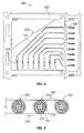
- FIG. 2is a side perspective view of a leadframe module for the receptacle connector and formed in accordance with an exemplary embodiment.
- FIG. 3is another side view of the leadframe module.
- FIG. 4illustrates a leadframe of the leadframe module formed in accordance with an exemplary embodiment.
- FIG. 5is a cross sectional view of a transmission line of the leadframe module formed in accordance with an exemplary embodiment.
- FIG. 6illustrates a machine used to manufacture leadframe modules and receptacle connectors.
- FIG. 7illustrates a method of manufacturing a leadframe module and a receptacle connector.
- FIG. 8illustrates a leadframe module formed in accordance with an exemplary embodiment.
- FIG. 9illustrates a leadframe module formed in accordance with an exemplary embodiment.
- FIG. 1is a perspective view of an exemplary embodiment of an electrical connector system 100 illustrating a receptacle connector 102 and a header connector 104 that may be directly mated together.
- the electrical connector system 100may be a high speed connector system passing high speed signals.
- the electrical connector system 100may include a plurality of transmission lines defined between circuit boards 106 , 108 .
- the system 100may form part of a network or server system.
- the electrical connector system 100may form part of a backplane system with the header connector 104 defining a backplane side of the system 100 and the receptacle connector 102 defining a daughtercard side of the system 100 . While the subject matter is described herein with reference to transmission lines for use in a high speed connector system, the subject matter is not limited to such application, and is but one example of an application that could use the transmission line structure described herein.
- the receptacle connector 102includes a housing 120 that holds a plurality of leadframe modules 122 . Any number of leadframe modules 122 may be provided to increase the density of the receptacle connector 102 .
- the leadframe modules 122each include a plurality of contacts 124 (shown in FIG. 2 ) that are received in the housing 120 for mating with the header connector 104 . In an exemplary embodiment, each contact 124 forms part of a shielded transmission line configured to convey data signals.
- the receptacle connector 102includes a mating end 128 and a mounting end 130 .
- the contacts 124are received in the housing 120 and held therein at the mating end 128 for mating to the header connector 104 .
- the contacts 124are arranged in a matrix of rows and columns. Any number of contacts 124 may be provided in the rows and columns.
- the contacts 124also extend to the mounting end 130 for mounting to the circuit board 106 .
- the mounting end 130may be substantially perpendicular to the mating end 128 , defining a right angle receptacle connector.
- the mating end 128 and mounting end 130may be parallel to each other, defining a mezzanine connector.
- the housing 120includes a plurality of signal contact openings 132 and a plurality of ground contact openings 134 at the mating end 128 .
- the contacts 124are received in corresponding signal contact openings 132 .
- a single contact 124is received in each signal contact opening 132 .
- the signal contact openings 132may also receive corresponding header signal contacts 144 therein when the receptacle and header connectors 102 , 104 are mated.
- the ground contact openings 134receive header shields 146 therein when the receptacle and header connectors 102 , 104 are mated.
- the ground contact openings 134receive grounding beams 228 (shown in FIG. 2 ) of the leadframe modules 122 that mate with the header shields 146 to electrically common the receptacle and header connectors 102 , 104 .
- the housing 120is manufactured from a dielectric material, such as a plastic material.
- the housing 120provides support for the leadframe modules 122 .
- the housing 120holds the leadframe modules 122 along parallel planes.
- the leadframe modules 122may be loaded into the rear of the housing 120 and extend rearward therefrom with portions of the leadframe modules 122 exposed.
- the housing 120may cover the entire leadframe modules 122 , such as to protect the leadframe modules 122 from damage.
- the leadframe modules 122may be loaded into the housing 120 through a top or a bottom of the housing 120 rather than through the rear of the housing 120 .
- the housing 120may include channels separated by walls that support and position the leadframe modules 122 within the housing 120 .
- the header connector 104includes a header housing 138 having walls 140 defining a chamber 142 .
- the header connector 104has a mating end 150 and a mounting end 152 that is mounted to the circuit board 108 .
- the mounting end 152may be substantially parallel to the mating end 150 .
- the receptacle connector 102is received in the chamber 142 through the mating end 150 .
- the housing 120engages the walls 140 to hold the receptacle connector 102 in the chamber 142 .
- the header signal contacts 144 and the header shields 146extend from a base wall 148 into the chamber 142 .
- the header signal contacts 144 and the header shields 146extend through the base wall 148 and are mounted to the circuit board 108 .
- the header signal contacts 144are arranged as differential pairs.
- the header shields 146are positioned between the differential pairs to provide electrical shielding between adjacent differential pairs.
- the header shields 146are C-shaped and provide shielding on three sides of the pair of header signal contacts 144 .
- the header signal contactsmay be arranged as single contacts with shielding at appropriate locations.
- the header shields 146may have other shapes in alternative embodiments.
- FIG. 2is a side perspective view of the leadframe module 122 formed in accordance with an exemplary embodiment.
- FIG. 3is another side view of the leadframe module 122 .
- the leadframe module 122includes a plurality of transmission lines 200 configured to convey data signals.
- the transmission lines 200may convey high speed data signals.
- the transmission lines 200are separated by air gaps 260 and do not include overmolded dielectric bodies holding all of the contacts 124 together as part of a common module, as is common of conventional contact modules.
- the transmission lines 200are individually electrically shielded.
- Each transmission line 200includes a corresponding contact 124 .
- the contact 124extends between a mating end 202 and a mounting end 204 .
- the mating ends 202 of the contacts 124are configured to be mated to corresponding mating contacts, such as the header signal contacts 144 (shown in FIG. 1 ).
- the mating ends 202each include a pair of opposed spring beams configured to receive the header signal contact 144 there between.
- Other types of mating interfacesmay be provided that the mating ends 202 in alternative embodiments.
- the mounting ends 204 of the contacts 124are configured to be terminated to corresponding conductors.
- the mounting ends 204may be terminated to traces, plated vias, or pads on the circuit board 106 (shown in FIG. 1 ) defining electrical conductors of the circuit board 106 .
- the mounting ends 204may be terminated to other types of conductors in alternative embodiments.
- the mounting ends 204may be terminated to corresponding wires or cables rather than the circuit board 106 .
- the mounting ends 204 of the contacts 124are solder pins configured to be inserted into plated vias of the circuit board 106 and soldered therein to make an electrical connection to the circuit board 106 .
- the mounting ends 204 of the contacts 124may be compliant pins or other types of contacts.
- the contacts 124include transition portions 206 extending between the mating and mounting ends 202 , 204 .
- the contacts 124are right angle contacts with the mating ends 202 being generally perpendicular to the mounting ends 204 .
- Each of the contacts 124have a different length than any adjacent contact 124 .
- the transition portions 206each have different length.
- the transmission lines 200include dielectric shells 210 coating corresponding contacts 124 .
- the transmission lines 200include outer shields 212 applied to corresponding dielectric shells 210 .
- the outer shields 212provide electrical shielding for corresponding contacts 124 .
- the dielectric shells 210electrically separate the contacts 124 from the corresponding outer shields 212 .
- the outer shields 212individually shield each of the contacts 124 along a majority of the length of the contacts 124 .
- the outer shields 212extend generally along the entire length of the transmission portions 206 of the contacts 124 .
- the transmission portions 206are entirely peripherally surrounded by corresponding dielectric shells 210 .
- the dielectric shells 210are entirely peripherally surrounded by corresponding outer shields 212 .
- the spacing between the outer shields 212 and the contacts 124may be controlled to control an impedance of the transmission lines 200 .
- the thickness of the dielectric shells 210may be controlled to define a separation distance between the outer shields 212 and the contacts 124 . Tight control of the positioning of the outer shields 212 with respect to the contacts 124 may achieve a target impedance for the transmission lines 200 to increase performance of the receptacle connector 102 .
- the transmission lines 200are separated by the air gaps 260 .
- the leadframe module 122includes ground plates 220 , 222 coupled to each of the transmission lines 200 .
- the ground plates 220 , 222are configured to be electrically connected to the outer shields 212 of the transmission lines 200 to electrically common each of the outer shields 212 .
- the ground plates 220 , 222provide mechanical support for the transmission lines 200 .
- the front ground plate 220is positioned proximate to the mating ends 202 of the contacts 124 and the bottom ground plate 222 is positioned proximate to the mounting ends 204 of the contacts 124 . Any number of ground plates may be used.
- the ground plates 220 , 222may be connected together to control the relative positions of the ground plates 220 , 222 .
- the ground platesmay extend along the entire transition portions 206 rather than be located just at the mating ends 202 and mounting end 204 .
- the ground plates 220 , 222are generally planar and extend along one side of the transmission lines 200 .
- the ground plates 220 , 222include fingers 224 that engage and hold the transmission lines 200 .
- the fingers 224may be crimped around the transmission lines 200 .
- the fingers 224may be stamped from the ground plates 220 , 222 and wrapped around the transmission lines 200 .
- the fingers 224directly engage the outer shields 212 to electrically connect the ground plates 220 , 222 to the transmission lines 200 .
- the bottom ground plate 222includes pins 226 extending therefrom.
- the pins 226are configured to be electrically connected to a ground plane of the circuit board 106 (shown in FIG. 1 ).
- the pins 226are compliant pins, such as eye of the needle contacts, that are configured to be loaded into vias of the circuit board 106 .
- the ground plate 220is directly grounded to the circuit board 106 .
- the ground plate 220provides a grounded electrical path between the outer shields 212 and the circuit board 106 .
- the front ground plate 220includes a plurality of ground beams 228 extended forward therefrom.
- the ground beams 228are positioned between adjacent contacts 124 .
- the ground beams 228extend along the mating ends 202 of the contacts 124 .
- the ground beams 228are configured to be electrically connected to corresponding header shields 146 (shown in FIG. 1 ) when the receptacle connector 102 is mated to the header connector 104 (both shown in FIG. 1 ).
- the ground beams 228may be deflectable such that the ground beams 228 may be biased against the header shields 146 when mated thereto.
- the ground beams 228create a grounded electrical path between the leadframe module 122 and the header connector 104 .
- the grounding beams 228provide electrical shielding between the mating ends 202 of the contacts 124 .
- the ground beam 228are stamped from the ground plate 222 and bent approximately perpendicularly with respect to the ground plate 222 to position the ground beams 228 in plane with the mating ends 202 of the contacts 124 .
- the leadframe module 122may be manufactured inexpensively and without the need for large tooling costs to design and develop the leadframe module 122 .
- conventional chickletsinclude over molded leadframes that include complicated shielding structures to provide electrical shielding between adjacent leads of the leadframe.
- the leadframe module 122is manufactured simply by coating the dielectric shells 210 over the contacts 124 and then applying the outer shields 212 to the dielectric shells 210 .
- the coating and shield applicationmay be easily applied to the contacts 124 irrespective of the size, shape, spacing or other physical parameters of the contacts 124 , whereas expensive tools and dies are needed to redesign the over mold of the leadframe of conventional chicklets when any modifications to the chicklet design are needed.
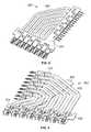
- FIG. 4illustrates a leadframe 250 formed in accordance with an exemplary embodiment.
- the leadframe 250may be stamped and formed from a stock metal sheet. After being stamped, the leadframe 250 includes a carrier 252 holding a plurality of the contacts 124 . The carrier 252 is later removed when the contacts 124 are singulated from one another.
- the transition portions 206 , mating ends 202 and mounting ends 204are all stamped and formed from the stock piece of metal and initially held together by the carrier 252 .
- the leadframe 250may be processed to form the transmission lines 200 (shown in FIGS. 2 and 3 ).
- the leadframe 250may be coated with a dielectric material to form the dielectric shells 210 (shown in FIGS. 2 and 3 ).
- the dielectric shells 210may be covered by conductive layers to form the outer shields 212 (shown in FIGS. 2 and 3 ).
- FIG. 5is a cross sectional view of the transmission line 200 formed in accordance with an exemplary embodiment.
- the transmission line 200includes the contact 124 , the dielectric shell 210 surrounding the contact 124 and the outer shield 212 surrounding the dielectric shell 210 .
- the air gaps 260are defined between adjacent transmission lines 200 .
- FIG. 6illustrates a machine used to manufacture leadframe modules 122 and receptacle connectors 102 .
- the leadframe modules 122are continuously manufactured using a reel system to pull the product through the machine 300 .
- the productis initially wound on a reel 302 and is feed through the machine 300 from the reel 302 .
- the productmay be a metal strip that is fed from the reel 302 .
- the machine 300includes a stamp 304 or press that is used to stamp the leadframe 250 (shown in FIG. 4 ) from the metal sheet. During the stamping, portions of the sheet may be removed and recycled leaving the contacts 124 (shown in FIG. 4 ) on the carrier 252 (shown in FIG. 4 ). The contacts 124 may be formed or bent during the stamping process.
- the machine 300includes a coating station 306 .
- the coating station 306may be a powder coating station.
- the coating station 306applies the dielectric shell 210 to the contacts 124 .
- the dielectric shell 210may be spray coated or may be coated using a fluidized bed.
- the leadframe 250is electrically grounded and electrically charged powder is applied to the leadframe 250 .
- portions of the leadframe 250may be masked or otherwise covered to resist coating in such areas.
- Such selective coatingapplies the dielectric shells 210 to the transition portions 206 as oppose to the mating ends 202 and mounting ends 204 .
- the conductive metal of the contacts 124remains exposed at the mating end 202 and mounting end 204 .
- the thickness of the dielectric shells 210may be controlled by controlling an amount of time that the product is at the coating station 306 , by changing the voltage applied to the leadframe 250 , by changing the material of the dielectric shells 210 and the like.
- the dielectric shells 210may have uniform thicknesses radially surrounding the entire contacts 124 .
- the machine 300may include other types of stations other than the coating station 306 to apply the dielectric material to the leadframe 250 .
- the dielectric materialmay be printed on the contacts 124 by a printing station, the dielectric material may be applied by a chemical vapor deposition process, by a physical vapor deposition process, by a dipping process, by a spraying process or by other processes known in the art to apply dielectric material to a substrate.
- the machine 300includes a post processing station 308 downstream of coating station 306 .
- the post processing station 308is used to process the leadframe 250 and the dielectric shell 210 to prepare the dielectric shells 210 for applying the outer shields 212 thereto.
- the dielectric shells 210may be thermally cured in a reflow oven to cure the dielectric material.
- the dielectric shells 210may be cleaned and or may be selectively removed from the contact 124 at the post processing station 308 .
- Other post processing functionsmay be performed at the post processing station 308 .
- the machine 300includes an application station 310 .
- the outer shields 212are applied to the dielectric shells 210 at the application station 310 .
- the application station 310may be a printing station, wherein conductive ink is printed directly on the dielectric shells 210 .
- the conductive inkmay be printed using a pad printer, an ink jet printer or another type of printer.
- the conducive layer defining the outer shields 212may be applied by other processes such as a spraying process, a plating process, or another type of process known in the art to apply a conductive layer to a substrate.
- the conductive layermay be processed to enhance characteristics of the conductive layer, such as to enhance the conductivity of the conductive layer.
- a conductive inkmay initially be applied to the dielectric shells to form a base conductive layer, and the base conductive layer may then be further processed, such as by electro-plating or electro-less plating.
- the application station 310applies the conductive layers to the dielectric shells 210 such that the conductive layers entirely peripherally surround the dielectric shells 210 .
- the contacts 124have 360° shielding providing by the outer shields 212 .
- the machine 300includes a second post processing station 312 after the application station 310 .
- the leadframe 250may be processed, such as to cure the outer shields 212 .
- the carrier 252may be removed, such as by stamping or cutting the carrier 252 from the contacts 124 .
- the ground plates 220may be coupled to the transmission lines 200 .
- the leadframe module 122may be inserted into the housing 120 to form the receptacle connector 102 .
- FIG. 7illustrates a method 320 of manufacturing a leadframe module 122 and a receptacle connector 102 .
- the methodincludes stamping a leadframe from a metal sheet.
- the contacts 124 thereofare initially held together by a carrier 252 , which is later removed.
- the methodincludes coating the contacts 124 with the dielectric material to form the dielectric shells 210 .
- the contacts 124may be selectively plated along certain portions of the contacts 124 .
- the transition portions 206may be coated with the dielectric material.
- the coatingmay be applied by powder coating the contacts 124 .
- the dielectric materialmay be sprayed onto the contacts 124 .
- the dielectric materialmay be dip coated by submersing the leadframe 250 in a bath or bed of electrically charged, powdered dielectric material. Other types of coating processes may be used in alternative embodiments.
- the dielectric shells 210may be applied to the contacts 124 by other processes other than coating in alternative embodiments.
- the dielectric shellsare cured.
- the leadframe 250may be passed through a reflow oven to thermally cure the dielectric material to form the dielectric shells 210 .
- the methodincludes applying conductive outer shields 212 to the dielectric shells 210 .
- the outer shields 212may be applied by printing conductive layer onto the dielectric shells 210 .
- the conductive layermay be applied by printing conductive ink on the dielectric shell 210 .
- a silver inkmaybe printed on the dielectric shell 210 .
- the conductive inkmay be pad printed, ink jet printed, or printed by other processes.
- the outer shields 212may be applied to the dielectric shells 210 by other processes in alternative embodiments.
- the methodincludes coupling the ground plates 222 , 220 to the outer shields 212 .
- the ground plates 220 , 222may be coupled to the outer shields 212 by crimping the fingers 224 to the outer shields 212 .
- Other securing means or processesmay be used in alternative embodiments, such as soldering the ground plates 220 , 222 to the outer shields 212 .
- the methodincludes singulating the contacts 124 from the carrier 252 of the leadframe 250 .
- the contacts 124may be singulated from the carrier 252 by punching, cutting, or otherwise removing the carrier 252 from the leadframe 250 . Once the contacts 124 are singulated, the contacts 124 are electrically isolated from each other such that the contacts 124 may convey different signals.
- the carrier 252is removed after the ground plates 220 , 222 are coupled to the outer shields 212 .
- the ground plates 220 , 222provide structural support for the transmission lines 200 and allow removal of the carrier 252 .
- the methodincludes loading the leadframe modules 122 into the housing 120 of the receptacle connector 102 .
- a plurality of the leadframe modules 122may be loaded into the housing 120 to form the receptacle connector 102 .
- FIG. 8illustrates a leadframe module 402 formed in accordance with an exemplary embodiment.
- the leadframe module 402is similar to the leadframe module 122 (shown in FIGS. 2 and 3 ) however the leadframe module 402 includes a single ground plate 404 .
- the ground plate 404is L-shaped and extends along mating and mounting ends of transmission lines 406 of the leadframe module 402 .
- the transmission lines 406may be more rigidly held together by having a single ground plate 404 rather than the front and bottom ground plates 220 , 222 (shown in FIGS. 2 and 3 ).
- FIG. 9illustrates a leadframe module 422 formed in accordance with an exemplary embodiment.
- the leadframe module 422is similar to the leadframe modules 122 (shown in FIGS. 2 and 3 ) and 402 (shown in FIG. 8 ), however the leadframe module 422 includes a single ground plate 424 having a plurality of spokes 426 .
- the ground plate 424extends along mating and mounting ends of transmission lines 428 of the leadframe module 422 as well as along central portions of the transmission lines 428 to provide additional support for the transmission lines 428 .
Landscapes
- Details Of Connecting Devices For Male And Female Coupling (AREA)
Abstract
Description
Claims (20)
Priority Applications (7)
| Application Number | Priority Date | Filing Date | Title |
|---|---|---|---|
| US13/658,340US9093800B2 (en) | 2012-10-23 | 2012-10-23 | Leadframe module for an electrical connector |
| TW102138202ATW201429058A (en) | 2012-10-23 | 2013-10-23 | Lead frame module for an electrical connector |
| PCT/US2013/066264WO2014066445A1 (en) | 2012-10-23 | 2013-10-23 | Leadframe module for an electrical connector |
| CN201380055139.XACN104737374B (en) | 2012-10-23 | 2013-10-23 | Lead frame modules for electrical connectors |
| EP13786107.6AEP2912726B1 (en) | 2012-10-23 | 2013-10-23 | Leadframe module for an electrical connector |
| KR1020157010160AKR101708577B1 (en) | 2012-10-23 | 2013-10-23 | Leadframe module for an electrical connector |
| JP2015539725AJP2015532523A (en) | 2012-10-23 | 2013-10-23 | Lead frame module for electrical connectors |
Applications Claiming Priority (1)
| Application Number | Priority Date | Filing Date | Title |
|---|---|---|---|
| US13/658,340US9093800B2 (en) | 2012-10-23 | 2012-10-23 | Leadframe module for an electrical connector |
Publications (2)
| Publication Number | Publication Date |
|---|---|
| US20140111960A1 US20140111960A1 (en) | 2014-04-24 |
| US9093800B2true US9093800B2 (en) | 2015-07-28 |
Family
ID=49517758
Family Applications (1)
| Application Number | Title | Priority Date | Filing Date |
|---|---|---|---|
| US13/658,340Active2033-10-29US9093800B2 (en) | 2012-10-23 | 2012-10-23 | Leadframe module for an electrical connector |
Country Status (7)
| Country | Link |
|---|---|
| US (1) | US9093800B2 (en) |
| EP (1) | EP2912726B1 (en) |
| JP (1) | JP2015532523A (en) |
| KR (1) | KR101708577B1 (en) |
| CN (1) | CN104737374B (en) |
| TW (1) | TW201429058A (en) |
| WO (1) | WO2014066445A1 (en) |
Cited By (11)
| Publication number | Priority date | Publication date | Assignee | Title |
|---|---|---|---|---|
| US9425556B1 (en)* | 2015-07-17 | 2016-08-23 | Tyco Electronics Corporation | Interconnection system and an electrical connector having resonance control |
| US9831608B1 (en)* | 2016-10-31 | 2017-11-28 | Te Connectivity Corporation | Electrical connector having ground shield that controls impedance at mating interface |
| US20180145437A1 (en)* | 2016-11-21 | 2018-05-24 | Tyco Electronics Corporation | Header contact for header connector of a communication system |
| US10236645B1 (en)* | 2017-10-26 | 2019-03-19 | All Best Precision Technology Co., Ltd. | Electrical connector |
| US10283914B1 (en)* | 2017-10-27 | 2019-05-07 | Te Connectivity Corporation | Connector assembly having a conductive gasket |
| US10559929B2 (en)* | 2018-01-25 | 2020-02-11 | Te Connectivity Corporation | Electrical connector system having a PCB connector footprint |
| CN110994284A (en)* | 2019-06-06 | 2020-04-10 | 富鼎精密工业(郑州)有限公司 | Electrical connector |
| US20200119498A1 (en)* | 2016-06-18 | 2020-04-16 | Molex, Llc | Selectively shielded connector channel |
| USD896763S1 (en)* | 2019-06-05 | 2020-09-22 | Starconn Electronic (Su Zhou) Co., Ltd. | Connector |
| US10916895B2 (en)* | 2018-01-29 | 2021-02-09 | Oupiin Electronic (Kunshan) Co., Ltd. | Double-shielded high-speed docking connector |
| US11081841B2 (en) | 2019-06-06 | 2021-08-03 | Fu Ding Precision Industrial (Zhengzhou) Co., Ltd. | Electrical connector haiving contact wafer equipped with transverse grounding bar |
Families Citing this family (8)
| Publication number | Priority date | Publication date | Assignee | Title |
|---|---|---|---|---|
| US9331448B2 (en)* | 2014-03-25 | 2016-05-03 | Tyco Electronics Corporation | Electrical connector having primary and secondary leadframes |
| US10186810B2 (en)* | 2017-01-27 | 2019-01-22 | Te Connectivity Corporation | Shielding structure for a contact module |
| CN110994227B (en)* | 2019-06-06 | 2021-06-18 | 富鼎精密工业(郑州)有限公司 | Electrical connector |
| CN114665330B (en)* | 2020-12-22 | 2023-01-06 | 华为技术有限公司 | A connector, function board and board-level structure |
| US11955752B2 (en) | 2021-02-02 | 2024-04-09 | Lotes Co., Ltd | Electrical connector |
| US12381361B2 (en) | 2021-05-12 | 2025-08-05 | Lotes Co., Ltd | Electrical connecting assembly |
| CN113937568B (en)* | 2021-09-08 | 2024-09-20 | 中航光电科技股份有限公司 | A signal connector |
| CN116191102A (en)* | 2023-02-23 | 2023-05-30 | 中航光电科技股份有限公司 | Terminal transmission unit of terminal module, terminal module and connector |
Citations (37)
| Publication number | Priority date | Publication date | Assignee | Title |
|---|---|---|---|---|
| US4401355A (en)* | 1981-07-01 | 1983-08-30 | Rca Corporation | Filtered connector |
| US4451107A (en)* | 1982-08-23 | 1984-05-29 | Amp Incorporated | High speed modular connector for printed circuit boards |
| US5554036A (en) | 1994-07-04 | 1996-09-10 | The Whitaker Corporation | Circuit board electrical connector |
| WO2001013468A2 (en) | 1999-08-17 | 2001-02-22 | Litton Systems, Inc. | High density electrical interconnect system having enhanced grounding and cross-talk reduction capability |
| US6231391B1 (en)* | 1999-08-12 | 2001-05-15 | Robinson Nugent, Inc. | Connector apparatus |
| WO2001057964A1 (en) | 2000-02-03 | 2001-08-09 | Teradyne, Inc. | Differential signal electrical connector |
| US6379188B1 (en)* | 1997-02-07 | 2002-04-30 | Teradyne, Inc. | Differential signal electrical connectors |
| US6409543B1 (en)* | 2001-01-25 | 2002-06-25 | Teradyne, Inc. | Connector molding method and shielded waferized connector made therefrom |
| US6431914B1 (en)* | 2001-06-04 | 2002-08-13 | Hon Hai Precision Ind. Co., Ltd. | Grounding scheme for a high speed backplane connector system |
| US6435914B1 (en)* | 2001-06-27 | 2002-08-20 | Hon Hai Precision Ind. Co., Ltd. | Electrical connector having improved shielding means |
| US6551140B2 (en)* | 2001-05-09 | 2003-04-22 | Hon Hai Precision Ind. Co., Ltd. | Electrical connector having differential pair terminals with equal length |
| US6692305B2 (en)* | 2001-11-28 | 2004-02-17 | Molex Incorporated | Flexural connector cover assembly mounting apparatus |
| US7191966B2 (en)* | 2003-08-04 | 2007-03-20 | Jeffrey David Sawczyszyn | Universal flexible powder coating tip/nozzle |
| US7442085B2 (en)* | 2005-01-14 | 2008-10-28 | Molex Incorporated | Filter connector |
| US7517250B2 (en)* | 2003-09-26 | 2009-04-14 | Fci Americas Technology, Inc. | Impedance mating interface for electrical connectors |
| US7553190B2 (en)* | 2005-03-31 | 2009-06-30 | Molex Incorporated | High-density, robust connector with dielectric insert |
| US20090191727A1 (en) | 2008-01-29 | 2009-07-30 | Hon Hai Precision Ind. Co., Ltd. | Electrical connector having improved terminal module |
| US7594826B2 (en)* | 2008-02-28 | 2009-09-29 | Fujitsu Component Limited | Connector |
| US7618289B2 (en)* | 2007-05-08 | 2009-11-17 | Tyco Electronics Corporation | Electrical connector with programmable lead frame |
| US7635278B2 (en)* | 2007-08-30 | 2009-12-22 | Fci Americas Technology, Inc. | Mezzanine-type electrical connectors |
| US7713088B2 (en)* | 2006-10-05 | 2010-05-11 | Fci | Broadside-coupled signal pair configurations for electrical connectors |
| US7731537B2 (en)* | 2007-06-20 | 2010-06-08 | Molex Incorporated | Impedance control in connector mounting areas |
| US7736182B2 (en)* | 2008-03-25 | 2010-06-15 | Hon Hai Precision Ind. Co., Ltd. | High speed electrical connector having improved housing |
| US7753731B2 (en)* | 2005-06-30 | 2010-07-13 | Amphenol TCS | High speed, high density electrical connector |
| US7758357B2 (en)* | 2008-12-02 | 2010-07-20 | Hon Hai Precision Ind. Co., Ltd. | Receptacle backplane connector having interface mating with plug connectors having different pitch arrangement |
| US7789705B2 (en)* | 2008-07-23 | 2010-09-07 | Tyco Electronics Corporation | Contact module for an electrical connector having propagation delay compensation |
| US7862344B2 (en)* | 2008-08-08 | 2011-01-04 | Tyco Electronics Corporation | Electrical connector having reversed differential pairs |
| US7867031B2 (en)* | 2007-06-20 | 2011-01-11 | Molex Incorporated | Connector with serpentine ground structure |
| US8002581B1 (en)* | 2010-05-28 | 2011-08-23 | Tyco Electronics Corporation | Ground interface for a connector system |
| US20110212650A1 (en)* | 2008-08-28 | 2011-09-01 | Molex Incorporated | Connector with overlapping ground configuration |
| US8147254B2 (en)* | 2007-11-15 | 2012-04-03 | Fci Americas Technology Llc | Electrical connector mating guide |
| US8157591B2 (en)* | 2008-12-05 | 2012-04-17 | Tyco Electronics Corporation | Electrical connector system |
| US8187034B2 (en)* | 2008-12-05 | 2012-05-29 | Tyco Electronics Corporation | Electrical connector system |
| US8192232B2 (en)* | 2009-09-15 | 2012-06-05 | Tyco Electronics Corporation | Connector assembly having an electrical compensation component |
| US8210877B2 (en)* | 2007-12-28 | 2012-07-03 | Fci | Modular connector |
| US8382524B2 (en)* | 2010-05-21 | 2013-02-26 | Amphenol Corporation | Electrical connector having thick film layers |
| US8398432B1 (en)* | 2011-11-07 | 2013-03-19 | Tyco Electronics Corporation | Grounding structures for header and receptacle assemblies |
Family Cites Families (9)
| Publication number | Priority date | Publication date | Assignee | Title |
|---|---|---|---|---|
| ES2070283T3 (en) | 1989-10-10 | 1995-06-01 | Whitaker Corp | CONTRAPLANE CONNECTOR WITH ADAPTED IMPEDANCES. |
| US5169343A (en)* | 1990-11-29 | 1992-12-08 | E. I. Du Pont De Nemours And Company | Coax connector module |
| DE19902034A1 (en)* | 1999-01-20 | 2000-07-27 | Continental Teves Ag & Co Ohg | Hydraulic unit, especially for hydraulic, slip-regulated motor vehicle braking system, has electrical plug connector containing plug in form of coaxial conductor and corresponding socket |
| JP3178455B2 (en)* | 1999-03-04 | 2001-06-18 | 日本電気株式会社 | connector |
| US6491545B1 (en)* | 2000-05-05 | 2002-12-10 | Molex Incorporated | Modular shielded coaxial cable connector |
| US6575761B1 (en)* | 2000-08-30 | 2003-06-10 | Molex Incorporated | Coaxial connector module and method of fabricating same |
| EP1393247A1 (en)* | 2001-05-17 | 2004-03-03 | Koninklijke Philips Electronics N.V. | Lead-frame configuration for chips |
| US7004793B2 (en)* | 2004-04-28 | 2006-02-28 | 3M Innovative Properties Company | Low inductance shielded connector |
| US7789676B2 (en)* | 2008-08-19 | 2010-09-07 | Tyco Electronics Corporation | Electrical connector with electrically shielded terminals |
- 2012
- 2012-10-23USUS13/658,340patent/US9093800B2/enactiveActive
- 2013
- 2013-10-23EPEP13786107.6Apatent/EP2912726B1/enactiveActive
- 2013-10-23WOPCT/US2013/066264patent/WO2014066445A1/enactiveApplication Filing
- 2013-10-23KRKR1020157010160Apatent/KR101708577B1/enactiveActive
- 2013-10-23TWTW102138202Apatent/TW201429058A/enunknown
- 2013-10-23JPJP2015539725Apatent/JP2015532523A/enactivePending
- 2013-10-23CNCN201380055139.XApatent/CN104737374B/enactiveActive
Patent Citations (38)
| Publication number | Priority date | Publication date | Assignee | Title |
|---|---|---|---|---|
| US4401355A (en)* | 1981-07-01 | 1983-08-30 | Rca Corporation | Filtered connector |
| US4451107A (en)* | 1982-08-23 | 1984-05-29 | Amp Incorporated | High speed modular connector for printed circuit boards |
| US5554036A (en) | 1994-07-04 | 1996-09-10 | The Whitaker Corporation | Circuit board electrical connector |
| US6379188B1 (en)* | 1997-02-07 | 2002-04-30 | Teradyne, Inc. | Differential signal electrical connectors |
| US6231391B1 (en)* | 1999-08-12 | 2001-05-15 | Robinson Nugent, Inc. | Connector apparatus |
| WO2001013468A2 (en) | 1999-08-17 | 2001-02-22 | Litton Systems, Inc. | High density electrical interconnect system having enhanced grounding and cross-talk reduction capability |
| WO2001057964A1 (en) | 2000-02-03 | 2001-08-09 | Teradyne, Inc. | Differential signal electrical connector |
| US6409543B1 (en)* | 2001-01-25 | 2002-06-25 | Teradyne, Inc. | Connector molding method and shielded waferized connector made therefrom |
| US6551140B2 (en)* | 2001-05-09 | 2003-04-22 | Hon Hai Precision Ind. Co., Ltd. | Electrical connector having differential pair terminals with equal length |
| US6431914B1 (en)* | 2001-06-04 | 2002-08-13 | Hon Hai Precision Ind. Co., Ltd. | Grounding scheme for a high speed backplane connector system |
| US6435914B1 (en)* | 2001-06-27 | 2002-08-20 | Hon Hai Precision Ind. Co., Ltd. | Electrical connector having improved shielding means |
| US6692305B2 (en)* | 2001-11-28 | 2004-02-17 | Molex Incorporated | Flexural connector cover assembly mounting apparatus |
| US7191966B2 (en)* | 2003-08-04 | 2007-03-20 | Jeffrey David Sawczyszyn | Universal flexible powder coating tip/nozzle |
| US7517250B2 (en)* | 2003-09-26 | 2009-04-14 | Fci Americas Technology, Inc. | Impedance mating interface for electrical connectors |
| US7442085B2 (en)* | 2005-01-14 | 2008-10-28 | Molex Incorporated | Filter connector |
| US7553190B2 (en)* | 2005-03-31 | 2009-06-30 | Molex Incorporated | High-density, robust connector with dielectric insert |
| US7753731B2 (en)* | 2005-06-30 | 2010-07-13 | Amphenol TCS | High speed, high density electrical connector |
| US7713088B2 (en)* | 2006-10-05 | 2010-05-11 | Fci | Broadside-coupled signal pair configurations for electrical connectors |
| US7618289B2 (en)* | 2007-05-08 | 2009-11-17 | Tyco Electronics Corporation | Electrical connector with programmable lead frame |
| US7867031B2 (en)* | 2007-06-20 | 2011-01-11 | Molex Incorporated | Connector with serpentine ground structure |
| US7731537B2 (en)* | 2007-06-20 | 2010-06-08 | Molex Incorporated | Impedance control in connector mounting areas |
| US7635278B2 (en)* | 2007-08-30 | 2009-12-22 | Fci Americas Technology, Inc. | Mezzanine-type electrical connectors |
| US8147254B2 (en)* | 2007-11-15 | 2012-04-03 | Fci Americas Technology Llc | Electrical connector mating guide |
| US8210877B2 (en)* | 2007-12-28 | 2012-07-03 | Fci | Modular connector |
| US20090191727A1 (en) | 2008-01-29 | 2009-07-30 | Hon Hai Precision Ind. Co., Ltd. | Electrical connector having improved terminal module |
| US7594826B2 (en)* | 2008-02-28 | 2009-09-29 | Fujitsu Component Limited | Connector |
| US7736182B2 (en)* | 2008-03-25 | 2010-06-15 | Hon Hai Precision Ind. Co., Ltd. | High speed electrical connector having improved housing |
| US7789705B2 (en)* | 2008-07-23 | 2010-09-07 | Tyco Electronics Corporation | Contact module for an electrical connector having propagation delay compensation |
| US7862344B2 (en)* | 2008-08-08 | 2011-01-04 | Tyco Electronics Corporation | Electrical connector having reversed differential pairs |
| US8342888B2 (en)* | 2008-08-28 | 2013-01-01 | Molex Incorporated | Connector with overlapping ground configuration |
| US20110212650A1 (en)* | 2008-08-28 | 2011-09-01 | Molex Incorporated | Connector with overlapping ground configuration |
| US7758357B2 (en)* | 2008-12-02 | 2010-07-20 | Hon Hai Precision Ind. Co., Ltd. | Receptacle backplane connector having interface mating with plug connectors having different pitch arrangement |
| US8157591B2 (en)* | 2008-12-05 | 2012-04-17 | Tyco Electronics Corporation | Electrical connector system |
| US8187034B2 (en)* | 2008-12-05 | 2012-05-29 | Tyco Electronics Corporation | Electrical connector system |
| US8192232B2 (en)* | 2009-09-15 | 2012-06-05 | Tyco Electronics Corporation | Connector assembly having an electrical compensation component |
| US8382524B2 (en)* | 2010-05-21 | 2013-02-26 | Amphenol Corporation | Electrical connector having thick film layers |
| US8002581B1 (en)* | 2010-05-28 | 2011-08-23 | Tyco Electronics Corporation | Ground interface for a connector system |
| US8398432B1 (en)* | 2011-11-07 | 2013-03-19 | Tyco Electronics Corporation | Grounding structures for header and receptacle assemblies |
Non-Patent Citations (1)
| Title |
|---|
| International Search Report, International Application No. PCT/US2013/066264, International Filing Date, Oct. 23, 2013. |
Cited By (14)
| Publication number | Priority date | Publication date | Assignee | Title |
|---|---|---|---|---|
| US9425556B1 (en)* | 2015-07-17 | 2016-08-23 | Tyco Electronics Corporation | Interconnection system and an electrical connector having resonance control |
| US20200119498A1 (en)* | 2016-06-18 | 2020-04-16 | Molex, Llc | Selectively shielded connector channel |
| US10879651B2 (en)* | 2016-06-18 | 2020-12-29 | Molex, Llc | Selectively shielded connector channel |
| US9831608B1 (en)* | 2016-10-31 | 2017-11-28 | Te Connectivity Corporation | Electrical connector having ground shield that controls impedance at mating interface |
| US20180145437A1 (en)* | 2016-11-21 | 2018-05-24 | Tyco Electronics Corporation | Header contact for header connector of a communication system |
| US10096924B2 (en)* | 2016-11-21 | 2018-10-09 | Te Connectivity Corporation | Header contact for header connector of a communication system |
| US10236645B1 (en)* | 2017-10-26 | 2019-03-19 | All Best Precision Technology Co., Ltd. | Electrical connector |
| US10283914B1 (en)* | 2017-10-27 | 2019-05-07 | Te Connectivity Corporation | Connector assembly having a conductive gasket |
| US10559929B2 (en)* | 2018-01-25 | 2020-02-11 | Te Connectivity Corporation | Electrical connector system having a PCB connector footprint |
| US10916895B2 (en)* | 2018-01-29 | 2021-02-09 | Oupiin Electronic (Kunshan) Co., Ltd. | Double-shielded high-speed docking connector |
| USD896763S1 (en)* | 2019-06-05 | 2020-09-22 | Starconn Electronic (Su Zhou) Co., Ltd. | Connector |
| CN110994284A (en)* | 2019-06-06 | 2020-04-10 | 富鼎精密工业(郑州)有限公司 | Electrical connector |
| CN110994284B (en)* | 2019-06-06 | 2021-06-18 | 富鼎精密工业(郑州)有限公司 | Electrical connector |
| US11081841B2 (en) | 2019-06-06 | 2021-08-03 | Fu Ding Precision Industrial (Zhengzhou) Co., Ltd. | Electrical connector haiving contact wafer equipped with transverse grounding bar |
Also Published As
| Publication number | Publication date |
|---|---|
| KR20150056854A (en) | 2015-05-27 |
| CN104737374B (en) | 2017-08-22 |
| WO2014066445A1 (en) | 2014-05-01 |
| EP2912726B1 (en) | 2018-01-17 |
| KR101708577B1 (en) | 2017-02-20 |
| TW201429058A (en) | 2014-07-16 |
| US20140111960A1 (en) | 2014-04-24 |
| JP2015532523A (en) | 2015-11-09 |
| CN104737374A (en) | 2015-06-24 |
| EP2912726A1 (en) | 2015-09-02 |
Similar Documents
| Publication | Publication Date | Title |
|---|---|---|
| US9093800B2 (en) | Leadframe module for an electrical connector | |
| US7789676B2 (en) | Electrical connector with electrically shielded terminals | |
| US8888530B2 (en) | Grounding structures for contact modules of connector assemblies | |
| US9923309B1 (en) | PCB connector footprint | |
| US9166320B1 (en) | Cable connector assembly | |
| US8690604B2 (en) | Receptacle assembly | |
| US8398434B2 (en) | Connector assembly | |
| US8398431B1 (en) | Receptacle assembly | |
| US10566740B2 (en) | Shielding structure for a contact module of an electrical connector | |
| US8360805B2 (en) | Connector banks arranged in parallel and floating manner | |
| US10790618B2 (en) | Electrical connector system having a header connector | |
| US8287322B2 (en) | Interface contact for an electrical connector | |
| US9543709B2 (en) | Insulating body with a shielding cross | |
| US10868392B2 (en) | Ground commoning conductors for electrical connector assemblies | |
| EP2945225A1 (en) | Electrical connectors having leadframes | |
| US11349236B2 (en) | High density communication system | |
| US9331448B2 (en) | Electrical connector having primary and secondary leadframes | |
| US20230411910A1 (en) | Direct plug hermaphroditic electrical connector assemblies | |
| EP3158612B1 (en) | Coaxial connector system | |
| CN109787001B (en) | Electrical connectors with low insertion loss conductors | |
| US20250070519A1 (en) | Ground bus for a cable card assembly of an electrical connector | |
| US20250260200A1 (en) | High speed and high density near chip connector |
Legal Events
| Date | Code | Title | Description |
|---|---|---|---|
| AS | Assignment | Owner name:TYCO ELECTRONICS CORPORATION, PENNSYLVANIA Free format text:ASSIGNMENT OF ASSIGNORS INTEREST;ASSIGNOR:LAUB, MICHAEL FREDRICK;REEL/FRAME:029176/0818 Effective date:20121022 | |
| STCF | Information on status: patent grant | Free format text:PATENTED CASE | |
| AS | Assignment | Owner name:TE CONNECTIVITY CORPORATION, PENNSYLVANIA Free format text:CHANGE OF NAME;ASSIGNOR:TYCO ELECTRONICS CORPORATION;REEL/FRAME:041350/0085 Effective date:20170101 | |
| MAFP | Maintenance fee payment | Free format text:PAYMENT OF MAINTENANCE FEE, 4TH YEAR, LARGE ENTITY (ORIGINAL EVENT CODE: M1551); ENTITY STATUS OF PATENT OWNER: LARGE ENTITY Year of fee payment:4 | |
| AS | Assignment | Owner name:TE CONNECTIVITY SERVICES GMBH, SWITZERLAND Free format text:CHANGE OF ADDRESS;ASSIGNOR:TE CONNECTIVITY SERVICES GMBH;REEL/FRAME:056514/0015 Effective date:20191101 Owner name:TE CONNECTIVITY SERVICES GMBH, SWITZERLAND Free format text:ASSIGNMENT OF ASSIGNORS INTEREST;ASSIGNOR:TE CONNECTIVITY CORPORATION;REEL/FRAME:056514/0048 Effective date:20180928 | |
| AS | Assignment | Owner name:TE CONNECTIVITY SOLUTIONS GMBH, SWITZERLAND Free format text:MERGER;ASSIGNOR:TE CONNECTIVITY SERVICES GMBH;REEL/FRAME:060885/0482 Effective date:20220301 | |
| MAFP | Maintenance fee payment | Free format text:PAYMENT OF MAINTENANCE FEE, 8TH YEAR, LARGE ENTITY (ORIGINAL EVENT CODE: M1552); ENTITY STATUS OF PATENT OWNER: LARGE ENTITY Year of fee payment:8 |