US9093753B2 - Artificial magnetic conductor - Google Patents
Artificial magnetic conductorDownload PDFInfo
- Publication number
- US9093753B2 US9093753B2US12/978,018US97801810AUS9093753B2US 9093753 B2US9093753 B2US 9093753B2US 97801810 AUS97801810 AUS 97801810AUS 9093753 B2US9093753 B2US 9093753B2
- Authority
- US
- United States
- Prior art keywords
- slot
- artificial magnetic
- magnetic conductor
- conductor
- ground layer
- Prior art date
- Legal status (The legal status is an assumption and is not a legal conclusion. Google has not performed a legal analysis and makes no representation as to the accuracy of the status listed.)
- Active, expires
Links
Images


Classifications
- H—ELECTRICITY
- H01—ELECTRIC ELEMENTS
- H01Q—ANTENNAS, i.e. RADIO AERIALS
- H01Q15/00—Devices for reflection, refraction, diffraction or polarisation of waves radiated from an antenna, e.g. quasi-optical devices
- H01Q15/0006—Devices acting selectively as reflecting surface, as diffracting or as refracting device, e.g. frequency filtering or angular spatial filtering devices
- H01Q15/006—Selective devices having photonic band gap materials or materials of which the material properties are frequency dependent, e.g. perforated substrates, high-impedance surfaces
- H01Q15/008—Selective devices having photonic band gap materials or materials of which the material properties are frequency dependent, e.g. perforated substrates, high-impedance surfaces said selective devices having Sievenpipers' mushroom elements
Definitions
- the present inventionrelates to an artificial magnetic conductor. More particularly, the present invention relates to an artificial magnetic conductor having a modified ground layer.
- An artificial magnetic conductoris a metamaterial representing a phenomenon that does not generally exist in nature, and has been in the spotlight as core technology that can overcome a physical limitation of existing technology.
- Such an artificial magnetic conductorhas a structure of a surface artificially having characteristics of a magnetic conductor in a specific frequency domain, unlike an electric conductor that can be seen naturally.
- the artificial magnetic conductoris formed with an electric conductor.
- a surface of the artificial magnetic conductoris formed in a protrusion structure to generate a capacitance component and an inductance component.
- These componentscan be represented with a frequency function, and surface impedance significantly increases by the components in a specific frequency domain.
- surface impedancehas a value of “0” and a reflection coefficient has a value of “ ⁇ 1” and thus an image current has an inverse phase
- surface impedancehas a very large value and a reflection coefficient has a value of “+1” and thus an image current has the same phase. Further, propagation of a surface wave can be suppressed due to high surface impedance.
- Such a conventional artificial magnetic conductorhas a general conductor plate that is not modified as a ground layer.
- a conventional artificial magnetic conductorthat has a general conductor plate as a ground layer and that is formed in the same grid cell size, in order to lower a frequency domain, a method of increasing capacitance between grid cells or increasing inductance is used.
- a frequency bandwidth operating as an artificial magnetic conductorbecomes narrow, and when increasing inductance, the size and weight of the artificial magnetic conductor structure increase.
- the present inventionhas been made in an effort to provide an artificial magnetic conductor structure having advantages of modifying a ground layer of the artificial magnetic conductor according to characteristics of a specific frequency domain, and reducing the size of the artificial magnetic conductor.
- An exemplary embodiment of the present inventionprovides an artificial magnetic conductor including: a conductor layer that is formed in a first direction and that comprises a plurality of grid cells; and a ground layer that is formed in a second direction that is opposite to the first direction and that generates a first frequency, wherein the first frequency is lower than a second frequency of a predetermined artificial magnetic conductor comprising a plurality of grid cells having the same size as that of the plurality of grid cells of the conductor layer and a conductor plate having a form that is not modified.
- an artificial magnetic conductorincluding: a conductor layer that includes a plurality of grid cells; a ground layer that is formed in a cross form structure to correspond to the conductor layer and that provides a different corresponding surface in the plurality of grid cells by the cross form; and a via that is formed between the conductor layer and the ground layer to electrically connect the conductor layer and the ground layer.
- an artificial magnetic conductorincluding: a conductor layer including a plurality of grid cells; a ground layer that is formed in a structure of a meandering form to correspond to the conductor layer and that provides a different surface corresponding to the plurality of grid cells by the meandering form; and a via that is formed between the conductor layer and the ground layer to electrically connect the conductor layer and the ground layer.
- an artificial magnetic conductorincluding: a conductor layer including a plurality of grid cells; a ground layer that is formed in a structure of a straight-line spiral form to correspond to the conductor layer and that provides a different surface corresponding to the plurality of grid cells by the straight-line spiral form; and a via that is formed between the conductor layer and the ground layer to electrically connect the conductor layer and the ground layer.
- FIG. 1is a diagram schematically illustrating a general artificial magnetic conductor.
- FIG. 2is a diagram illustrating an example of reflection phase frequency characteristics of the general artificial magnetic conductor of FIG. 1 .
- FIG. 3is a diagram illustrating an example of an artificial magnetic conductor according to an exemplary embodiment of the present invention.
- FIG. 4is a diagram schematically illustrating an equivalent circuit of the artificial magnetic conductor of FIG. 3 .
- FIG. 5is a diagram illustrating an example of frequency characteristics of the artificial magnetic conductor of FIG. 3 .
- FIG. 6is a diagram illustrating another example of a ground layer of the artificial magnetic conductor of FIG. 3 .
- FIG. 7is a diagram illustrating an example of frequency characteristics of the artificial magnetic conductor of FIG. 6 .
- FIG. 8is a diagram illustrating another example of a ground layer of the artificial magnetic conductor of FIG. 3 .
- FIG. 9is a diagram illustrating an example of frequency characteristics of the artificial magnetic conductor of FIG. 8 .
- FIG. 1is a diagram schematically illustrating a general artificial magnetic conductor
- FIG. 2is a diagram illustrating an example of reflection phase frequency characteristics of the general artificial magnetic conductor of FIG. 1 .
- a general artificial magnetic conductor 10includes a ground layer 11 , a conductor layer 13 including grid cells 12 , and a via 14 .
- phase distribution of a reflection coefficientchanges according to a change of surface impedance that is generated with a capacitance component and an inductance component between the grid cells 12 of the general artificial magnetic conductor 10 . That is, the general artificial magnetic conductor 10 has a property of a complete magnetic conductor in a frequency in which a phase of a reflection coefficient becomes 0°.
- the general artificial magnetic conductor 10has a general conductor plate that is not deformed as the ground layer 11 , and lowers a frequency domain by operating as the artificial magnetic conductor 10 in a given size of the grid cells 12 , or operates as the artificial magnetic conductor 10 in a specific frequency domain and thus has a limitation in decreasing a size thereof.
- the general artificial magnetic conductor 10 having the grid cells 12 of the same sizein order to lower a frequency domain, a method of increasing capacitance between the grid cells 12 or increasing inductance by increasing a distance between the ground layer 11 and the conductor layer 13 is used.
- a frequency bandwidthbecomes narrow
- the size and weight of the artificial magnetic conductor 10increase.
- an artificial magnetic conductorin which a ground layer of the artificial magnetic conductor is modified in various forms is provided, and will be described in detail with referring to FIGS. 3 to 9 .
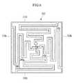
- FIG. 3is a diagram illustrating an example of an artificial magnetic conductor according to an exemplary embodiment of the present invention.
- FIG. 4is a diagram schematically illustrating an equivalent circuit of the artificial magnetic conductor of FIG. 3
- FIG. 5is a diagram illustrating an example of frequency characteristics of the artificial magnetic conductor of FIG. 3 .
- an artificial magnetic conductor 20includes a conductor layer 100 , a ground layer 200 , and a via 300 .
- the conductor layer 100is positioned in a first direction of the artificial magnetic conductor 20 , and includes grid cells 110 having an electrical capacity.
- the size and gap of the grid cells 110are uniformly formed, but the present invention is not limited thereto, and a size and gap of the grid cells 110 may not be uniformly formed.
- the ground layer 200is positioned in a second direction that is opposite to the first direction of the artificial magnetic conductor 20 , and is electrically connected to the grid cells 110 through the via 300 .
- the ground layer 200has a structure in which the ground layer 11 of the general artificial magnetic conductor 10 that is shown in FIG. 1 is modified in a cross form.
- the ground layer 200includes frame slots 210 a , 210 b , 210 c , and 210 d that are formed in a quadrangular form, a first slot 220 that connects the centers of each of the frame slots 210 c and 210 d , and a second slot 230 that connects the centers of each of the frame slots 210 a and 210 b .
- the slot 220 and the slot 230are connected through a center point CP of the ground layer 200 in a cross form.
- the via 300is electrically connected between the conductor layer 100 and the ground layer 200 .
- An equivalent circuit of the artificial magnetic conductor 20can be formed, as shown in FIG. 4 , and in the artificial magnetic conductor 20 , a capacitance component is generated by proximity between the grid cells 110 that are adjacent to the conductor layer 100 , and an inductance component is generated by a loop structure within the grid cells 110 .
- a lattice structure that is formed through the grid cells 110 in the artificial magnetic conductor 20has resonance characteristics by a capacitance component and an inductance component between the grid cells 110 .
- Surface impedance by a capacitance component C and an inductance component L that are generated in the lattice structureare represented by Equation 1.
- Z sis surface impedance of the conductor layer 100 that is generated by a lattice structure
- Cis a capacitance component that is generated in the lattice structure
- Lis an inductance component that is generated in the lattice structure.
- a reflection coefficient in a surface of the conductor layer 100is represented by Equation 2, and a phase of a reflection coefficient is represented by Equation 3.
- ⁇is free space impedance
- ⁇is a phase of a reflection coefficient
- a frequency bandwidth of the artificial magnetic conductor 20is defined as a frequency domain having a value within ⁇ 90° about a frequency in which a phase of a reflection coefficient is 0°.
- a frequency in which a phase of a reflection coefficient of the artificial magnetic conductor 20 becomes 0°is represented by Equation 4, and a frequency bandwidth thereof is represented by Equation 5.
- Cis a capacitance component that is generated in the lattice structure
- Lis an inductance component that is generated in the lattice structure
- ⁇is free space impedance
- a frequency in which a phase of a reflection coefficient of the artificial magnetic conductor 20 becomes 0°is inversely proportional to an inductance component L and a capacitance component C of the grid cells 110 . Therefore, when increasing inductance or capacitance by modifying a structure of the grid cells 110 , the frequency can be reduced.
- Equation 5because a frequency bandwidth of the artificial magnetic conductor 20 is proportional to the inductance component L and is inversely proportional to the capacitance component C, the bandwidth decreases when lowering the frequency so that a phase of a reflection coefficient of the artificial magnetic conductor 20 becomes 0° by increasing the capacitance component C, and when increasing the frequency so that a phase of a reflection coefficient of the artificial magnetic conductor 20 may become 0° by increasing the inductance component L, the bandwidth increases.
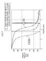
- a structure and size of the grid cells 110 that determine the capacitance component C and the inductance component L according to such a lattice structureare the same in the artificial magnetic conductor 20 and the general artificial magnetic conductor 10 , as shown in FIG. 5 , in the artificial magnetic conductor 20 , a frequency in which a phase of a reflection coefficient becomes 0° by the ground layer 200 that is formed in a cross form becomes 1.7 GHz and is smaller than 2.21 GHz, which is a frequency in the ground layer 11 of the general artificial magnetic conductor 10 .
- FIG. 6is a diagram illustrating another example of a ground layer of the artificial magnetic conductor of FIG. 3 .
- FIG. 7is a diagram illustrating an example of frequency characteristics of the artificial magnetic conductor of FIG. 6 .
- a ground layer 200 ′ of the artificial magnetic conductor 20is formed in a structure of a meandering form.
- the ground layer 200 ′includes frame slots 210 a , 210 b , 210 c , and 210 d that are formed in a quadrangular form, and slots 240 a , 240 b , 240 c , and 240 d of a meandering form.
- the frame slot 210 a of the ground layer 200 ′is connected to the slot 240 a of a meandering form that is connected to a center point CP
- the frame slot 210 bis connected to the slot 240 b of a meandering form that is connected to the center point CP
- the frame slot 210 cis connected to the slot 240 c of a meandering form that is connected to the center point CP
- the frame slot 210 dis connected to the slot 240 d of a meandering form that is connected to the center point CP.
- the slot 240 a and the slot 240 bare symmetrically formed with the center point CP interposed therebetween
- the slot 240 c and the slot 240 dare symmetrically formed with the center point CP interposed therebetween.
- the frequency in which the phase of a reflection coefficient becomes 0°becomes 1.36 GHz by the ground layer 200 ′ that is formed in the meandering form and is smaller than 2.21 GHz, which is the frequency in the ground layer 11 of the general artificial magnetic conductor 10 .
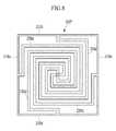
- FIG. 8is a diagram illustrating another example of a ground layer of the artificial magnetic conductor of FIG. 3 .
- FIG. 9is a diagram illustrating an example of frequency characteristics of the artificial magnetic conductor of FIG. 8 .
- a ground layer 200 ′′ of the artificial magnetic conductor 20is formed in a structure of a straight-line spiral form.
- the ground layer 200 ′′includes frame slots 210 a , 210 b , 210 c , and 210 d that are formed in a quadrangular form, and slots 250 a , 250 b , 250 c , and 250 d of a straight-line spiral form.
- the frame slot 210 a of the ground layer 200 ′′is connected to the slot 250 a of a straight-line spiral form that is connected to a center point CP
- the frame slot 210 bis connected to the slot 250 b of a straight-line spiral form that is connected to the center point CP
- the frame slot 210 cis connected to the slot 250 c of a straight-line spiral form that is connected to the center point CP
- the frame slot 210 dis connected to the slot 250 d of a straight-line spiral form that is connected to the center point CP.
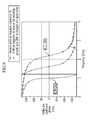
- the frequency in which the phase of a reflection coefficient becomes 0°becomes 0.99 GHz by the ground layer 200 ′ that is formed in the straight-line spiral form and is smaller than 2.21 GHz, which is the frequency in the ground layer 11 of the general artificial magnetic conductor 10 .
- the ground layer 200 of the artificial magnetic conductor 20is formed in a structure of a cross form, a structure of a meandering form, and a structure of a straight-line spiral form, but the present invention is not limited thereto, and the ground layer 200 can have various forms within a range that can be operated with the artificial magnetic conductor 20 .
- the artificial magnetic conductor 20is formed and thus the grid cells can be designed to operate with an artificial magnetic conductor in a lower frequency of the same condition, and a structure operating with an artificial magnetic conductor in a specific frequency can be formed in a smaller size.
- inductancecan increase and thus a frequency domain operating as the artificial magnetic conductor in the same grid cell size can be lowered.
- inductanceis increased and thus bandwidth can increase.
- a ground layer of grid cells of an artificial magnetic conductorin various forms, improved characteristics such as a low cost, a light weight, a thin thickness, an easy manufacturing process, and heat resistance can be obtained.
- An exemplary embodiment of the present inventionmay not only be embodied through the above-described apparatus and method, but may also be embodied through a program that realizes a function corresponding to a configuration of the exemplary embodiment of the present invention or a recording medium on which the program is recorded.
Landscapes
- Physics & Mathematics (AREA)
- Optics & Photonics (AREA)
- Coils Or Transformers For Communication (AREA)
Abstract
Description

Claims (2)
Applications Claiming Priority (4)
| Application Number | Priority Date | Filing Date | Title |
|---|---|---|---|
| KR10-2010-0006191 | 2010-01-22 | ||
| KR20100006191 | 2010-01-22 | ||
| KR1020100026784AKR101319611B1 (en) | 2010-01-22 | 2010-03-25 | Artificial magnetic conductor |
| KR10-2010-0026784 | 2010-03-25 |
Publications (2)
| Publication Number | Publication Date |
|---|---|
| US20110181490A1 US20110181490A1 (en) | 2011-07-28 |
| US9093753B2true US9093753B2 (en) | 2015-07-28 |
Family
ID=44308572
Family Applications (1)
| Application Number | Title | Priority Date | Filing Date |
|---|---|---|---|
| US12/978,018Active2034-03-08US9093753B2 (en) | 2010-01-22 | 2010-12-23 | Artificial magnetic conductor |
Country Status (1)
| Country | Link |
|---|---|
| US (1) | US9093753B2 (en) |
Cited By (7)
| Publication number | Priority date | Publication date | Assignee | Title |
|---|---|---|---|---|
| US20150244080A1 (en)* | 2011-04-07 | 2015-08-27 | Hrl Laboratories, Llc. | Polarization independent active artificial magentic conductor |
| US9407239B2 (en) | 2011-07-06 | 2016-08-02 | Hrl Laboratories, Llc | Wide bandwidth automatic tuning circuit |
| US9425769B1 (en) | 2014-07-18 | 2016-08-23 | Hrl Laboratories, Llc | Optically powered and controlled non-foster circuit |
| US9559012B1 (en) | 2013-09-30 | 2017-01-31 | Hrl Laboratories, Llc | Gallium nitride complementary transistors |
| US9705201B2 (en) | 2014-02-24 | 2017-07-11 | Hrl Laboratories, Llc | Cavity-backed artificial magnetic conductor |
| US10103445B1 (en) | 2012-06-05 | 2018-10-16 | Hrl Laboratories, Llc | Cavity-backed slot antenna with an active artificial magnetic conductor |
| US11024952B1 (en) | 2019-01-25 | 2021-06-01 | Hrl Laboratories, Llc | Broadband dual polarization active artificial magnetic conductor |
Families Citing this family (5)
| Publication number | Priority date | Publication date | Assignee | Title |
|---|---|---|---|---|
| EP2544306B1 (en)* | 2011-03-15 | 2018-09-05 | Kuang-Chi Innovative Technology Ltd. | Artificial microstructure and artificial electromagnetic material using same |
| CN103296404A (en)* | 2012-02-29 | 2013-09-11 | 深圳光启创新技术有限公司 | Metamaterial antenna housing |
| US8977208B2 (en) | 2012-11-19 | 2015-03-10 | Broadcom Corporation | Reflective beamforming for performing chip-to-chip and other communications |
| KR102017491B1 (en) | 2013-08-01 | 2019-09-04 | 삼성전자주식회사 | Antenna device and electronic device with the same |
| CN115207640B (en)* | 2022-08-26 | 2025-05-16 | 合肥工业大学 | A bandpass frequency selective surface |
Citations (10)
| Publication number | Priority date | Publication date | Assignee | Title |
|---|---|---|---|---|
| US6483480B1 (en)* | 2000-03-29 | 2002-11-19 | Hrl Laboratories, Llc | Tunable impedance surface |
| US6512494B1 (en)* | 2000-10-04 | 2003-01-28 | E-Tenna Corporation | Multi-resonant, high-impedance electromagnetic surfaces |
| US6525693B2 (en) | 2000-10-10 | 2003-02-25 | Fiat Auto S.P.A. | Device for the reception of GPS position signals |
| US20030071763A1 (en)* | 2001-08-06 | 2003-04-17 | Mckinzie William E. | Low frequency enhanced frequency selective surface technology and application |
| US6917343B2 (en) | 2001-09-19 | 2005-07-12 | Titan Aerospace Electronics Division | Broadband antennas over electronically reconfigurable artificial magnetic conductor surfaces |
| KR100753830B1 (en) | 2006-04-04 | 2007-08-31 | 한국전자통신연구원 | High impedance surface structure using artificial magnetic conductor, antenna device and electromagnetic device using the structure |
| KR20080039178A (en) | 2006-10-31 | 2008-05-07 | 한국전자통신연구원 | Tag antenna for conductor recognition using artificial magnetic conductor and wireless recognition system using tag antenna |
| KR20090065257A (en) | 2007-12-17 | 2009-06-22 | 한국전자통신연구원 | Antenna device with electromagnetic wave stop |
| US20100127943A1 (en)* | 2008-11-25 | 2010-05-27 | Kabushiki Kaisha Toshiba | Antenna apparatus and wireless communication device |
| US8325104B2 (en)* | 2006-12-04 | 2012-12-04 | Electronics And Telecommunications Research Institute | Dipole tag antenna structure mountable on metallic objects using artificial magnetic conductor for wireless identification and wireless identification system using the dipole tag antenna structure |
- 2010
- 2010-12-23USUS12/978,018patent/US9093753B2/enactiveActive
Patent Citations (13)
| Publication number | Priority date | Publication date | Assignee | Title |
|---|---|---|---|---|
| US6483480B1 (en)* | 2000-03-29 | 2002-11-19 | Hrl Laboratories, Llc | Tunable impedance surface |
| US6512494B1 (en)* | 2000-10-04 | 2003-01-28 | E-Tenna Corporation | Multi-resonant, high-impedance electromagnetic surfaces |
| US6525693B2 (en) | 2000-10-10 | 2003-02-25 | Fiat Auto S.P.A. | Device for the reception of GPS position signals |
| US20030071763A1 (en)* | 2001-08-06 | 2003-04-17 | Mckinzie William E. | Low frequency enhanced frequency selective surface technology and application |
| US6917343B2 (en) | 2001-09-19 | 2005-07-12 | Titan Aerospace Electronics Division | Broadband antennas over electronically reconfigurable artificial magnetic conductor surfaces |
| US20090201220A1 (en) | 2006-04-04 | 2009-08-13 | Dong-Ho Kim | High impedance surface structure using artificial magnetic conductor, and antenna and electromagnetic device using the same structure |
| KR100753830B1 (en) | 2006-04-04 | 2007-08-31 | 한국전자통신연구원 | High impedance surface structure using artificial magnetic conductor, antenna device and electromagnetic device using the structure |
| KR20080039178A (en) | 2006-10-31 | 2008-05-07 | 한국전자통신연구원 | Tag antenna for conductor recognition using artificial magnetic conductor and wireless recognition system using tag antenna |
| US20100001080A1 (en) | 2006-10-31 | 2010-01-07 | Electronics And Telecommunications Research Institute | Tag antenna structure for wireless identification and wireless identification system using the tag antenna structure |
| US8325104B2 (en)* | 2006-12-04 | 2012-12-04 | Electronics And Telecommunications Research Institute | Dipole tag antenna structure mountable on metallic objects using artificial magnetic conductor for wireless identification and wireless identification system using the dipole tag antenna structure |
| KR20090065257A (en) | 2007-12-17 | 2009-06-22 | 한국전자통신연구원 | Antenna device with electromagnetic wave stop |
| US20090201212A1 (en) | 2007-12-17 | 2009-08-13 | Electronics And Telecommunications Research Institute | Antenna system having electromagnetic bandgap |
| US20100127943A1 (en)* | 2008-11-25 | 2010-05-27 | Kabushiki Kaisha Toshiba | Antenna apparatus and wireless communication device |
Cited By (8)
| Publication number | Priority date | Publication date | Assignee | Title |
|---|---|---|---|---|
| US20150244080A1 (en)* | 2011-04-07 | 2015-08-27 | Hrl Laboratories, Llc. | Polarization independent active artificial magentic conductor |
| US9379448B2 (en)* | 2011-04-07 | 2016-06-28 | Hrl Laboratories, Llc | Polarization independent active artificial magnetic conductor |
| US9407239B2 (en) | 2011-07-06 | 2016-08-02 | Hrl Laboratories, Llc | Wide bandwidth automatic tuning circuit |
| US10103445B1 (en) | 2012-06-05 | 2018-10-16 | Hrl Laboratories, Llc | Cavity-backed slot antenna with an active artificial magnetic conductor |
| US9559012B1 (en) | 2013-09-30 | 2017-01-31 | Hrl Laboratories, Llc | Gallium nitride complementary transistors |
| US9705201B2 (en) | 2014-02-24 | 2017-07-11 | Hrl Laboratories, Llc | Cavity-backed artificial magnetic conductor |
| US9425769B1 (en) | 2014-07-18 | 2016-08-23 | Hrl Laboratories, Llc | Optically powered and controlled non-foster circuit |
| US11024952B1 (en) | 2019-01-25 | 2021-06-01 | Hrl Laboratories, Llc | Broadband dual polarization active artificial magnetic conductor |
Also Published As
| Publication number | Publication date |
|---|---|
| US20110181490A1 (en) | 2011-07-28 |
Similar Documents
| Publication | Publication Date | Title |
|---|---|---|
| US9093753B2 (en) | Artificial magnetic conductor | |
| Mosallaei et al. | Design and modeling of patch antenna printed on magneto-dielectric embedded-circuit metasubstrate | |
| Ghosh et al. | Polarisation‐insensitive and wide‐angle multi‐layer metamaterial absorber with variable bandwidths | |
| Wu et al. | Dual‐band multiple input multiple output antenna with slitted ground | |
| Suntives et al. | Miniaturization and isolation improvement of a multiple‐patch antenna system using electromagnetic bandgap structures | |
| Fujimoto et al. | Wideband rectangular printed monopole antenna for circular polarisation | |
| Karimian et al. | Design of a compact ultra‐wide‐band monopole antenna with band rejection characteristics | |
| Alibakhshi Kenari | Design and modeling of new UWB metamaterial planar cavity antennas with shrinking of the physical size for modern transceivers | |
| Yang et al. | A bandpass frequency selective surface with a low cross-polarization based on cavities with a hybrid boundary | |
| Aeini et al. | Compact, wideband‐printed quasi‐Yagi antenna using spiral metamaterial resonators | |
| Kim et al. | Design of a compact dualband quasi‐isotropic antenna | |
| Sim et al. | Design of electromagnetic wave absorber using periodic structure and method to broaden its bandwidth based on equivalent circuit‐based analysis | |
| Yoon et al. | A Rectangular Ring, Open‐Ended Monopole Antenna with Two Symmetric Strips for WLAN and WiMAX Applications | |
| Altaf et al. | Wideband circularly polarized spidron fractal slot antenna with an embedded patch | |
| Fakhte et al. | Compact uniaxial anisotropic dielectric resonator antenna operating at higher order radiating mode | |
| Xia et al. | Miniaturized Wideband Single‐Layer CP Metasurface Antenna Using CPW‐Fed | |
| US20190173147A1 (en) | Metaconductor skins for low loss rf conductors | |
| Bala et al. | Dual mode metamaterial antenna for wideband applications | |
| Ghosh et al. | Meander line‐based low profile RIS with defected ground and its use in patch antenna miniaturization for wireless applications | |
| KR101319611B1 (en) | Artificial magnetic conductor | |
| Safwat et al. | High-impedance wire | |
| Luo et al. | Miniaturised design of coplanar waveguide‐fed broadband circularly polarised slot antenna | |
| Matzner et al. | Can λ/4 Radiators Be Really Isotropic? | |
| Kim et al. | Enhanced gain and miniaturisation method of stacked dielectric resonator antenna using metallic cap | |
| Wong et al. | On‐frame gap‐coupled half‐loop antenna with a narrow ground clearance for the LTE smartphone |
Legal Events
| Date | Code | Title | Description |
|---|---|---|---|
| AS | Assignment | Owner name:ELECTRONICS AND TELECOMMUNICATIONS RESEARCH INSTIT Free format text:ASSIGNMENT OF ASSIGNORS INTEREST;ASSIGNORS:JUNG, YOUNG BAE;EOM, SOON YOUNG;JEON, SOON IK;AND OTHERS;REEL/FRAME:025564/0789 Effective date:20101020 Owner name:INDUSTRY-ACADEMIC COOPERATION FOUNDATION, YONSEI U Free format text:ASSIGNMENT OF ASSIGNORS INTEREST;ASSIGNORS:JUNG, YOUNG BAE;EOM, SOON YOUNG;JEON, SOON IK;AND OTHERS;REEL/FRAME:025564/0789 Effective date:20101020 | |
| AS | Assignment | Owner name:INDUSTRY-ACADEMIC COOPERATION FOUNDATION, YONSEI U Free format text:ASSIGNMENT OF ASSIGNORS INTEREST;ASSIGNORS:ELECTRONICS AND TELECOMMUNICATIONS RESEARCH INSTITUTE;INDUSTRY-ACADEMIC COOPERATION FOUNDATION, YONSEI UNIVERSITY;SIGNING DATES FROM 20140901 TO 20140923;REEL/FRAME:033883/0214 | |
| FEPP | Fee payment procedure | Free format text:PAYOR NUMBER ASSIGNED (ORIGINAL EVENT CODE: ASPN); ENTITY STATUS OF PATENT OWNER: SMALL ENTITY | |
| STCF | Information on status: patent grant | Free format text:PATENTED CASE | |
| MAFP | Maintenance fee payment | Free format text:PAYMENT OF MAINTENANCE FEE, 4TH YR, SMALL ENTITY (ORIGINAL EVENT CODE: M2551); ENTITY STATUS OF PATENT OWNER: SMALL ENTITY Year of fee payment:4 | |
| MAFP | Maintenance fee payment | Free format text:PAYMENT OF MAINTENANCE FEE, 8TH YR, SMALL ENTITY (ORIGINAL EVENT CODE: M2552); ENTITY STATUS OF PATENT OWNER: SMALL ENTITY Year of fee payment:8 |