US9092388B2 - Bus width negotiation - Google Patents
Bus width negotiationDownload PDFInfo
- Publication number
- US9092388B2 US9092388B2US13/009,559US201113009559AUS9092388B2US 9092388 B2US9092388 B2US 9092388B2US 201113009559 AUS201113009559 AUS 201113009559AUS 9092388 B2US9092388 B2US 9092388B2
- Authority
- US
- United States
- Prior art keywords
- storage device
- pin
- bus width
- bus
- indicate
- Prior art date
- Legal status (The legal status is an assumption and is not a legal conclusion. Google has not performed a legal analysis and makes no representation as to the accuracy of the status listed.)
- Active, expires
Links
Images


Classifications
- G—PHYSICS
- G06—COMPUTING OR CALCULATING; COUNTING
- G06F—ELECTRIC DIGITAL DATA PROCESSING
- G06F13/00—Interconnection of, or transfer of information or other signals between, memories, input/output devices or central processing units
- G06F13/14—Handling requests for interconnection or transfer
- G06F13/16—Handling requests for interconnection or transfer for access to memory bus
- G06F13/1668—Details of memory controller
- G06F13/1694—Configuration of memory controller to different memory types
- G—PHYSICS
- G06—COMPUTING OR CALCULATING; COUNTING
- G06F—ELECTRIC DIGITAL DATA PROCESSING
- G06F13/00—Interconnection of, or transfer of information or other signals between, memories, input/output devices or central processing units
- G06F13/14—Handling requests for interconnection or transfer
- G06F13/16—Handling requests for interconnection or transfer for access to memory bus
- G06F13/1668—Details of memory controller
- G06F13/1678—Details of memory controller using bus width
Definitions
- Embodiments of the present inventionrelate generally to the field of data storage and more particularly to transferring data to and from a data storage device.
- removable data storage devicessuch as flash memory cards for saving digital content such as photos, music, video or personal data.
- flash memory card standardshave been developed, including MultiMediaCard (MMC), Secure Digital Card (SD Card), and Memory Stick, for example.
- MMCMultiMediaCard
- SD CardSecure Digital Card
- Memory StickMemory Stick
- non-removable data storage devicesi.e. “fixed” storage devices
- MMC BGAball grid array multimedia card
- iNANDfrom SanDisk
- the specifications for the removable storage devicesoriginally limited the communication bus between a host system and the removable data storage devices to a single data line (e.g. the x1 data bus, wherein a data bus can comprise one or more data lines) in order to keep the number of physical connections between the data storage devices and the host to a minimum, wherein such physical connections are referred to herein as contacts, with one example of a contact being a pin.
- a contactis referred to herein as contacts, with one example of a contact being a pin.
- the size of the digital content files stored on the data storage deviceshas grown so has the data storage capacity of the data storage devices. As a result, the need for faster data transfer between the host and the data storage devices has also increased.
- One method for increasing the data transfer rateis increasing the data bus width.
- the data bus widthmay be increased from x1 to x4 or x8.
- the x1, x4 and x8connote the number of data lines.
- Existing techniques for establishing a wider bus communicationinclude initiating communications between the host and the data storage devices over a default x1 data bus. The host then queries the data storage devices over the x1 data bus to extract information about alternative bus configurations supported by the device. If both the host and the data storage device support a wider bus, the host issues a command and the data storage device and the host are re-configured to operate using the wider bus. Unfortunately, this method is somewhat cumbersome when implemented.
- the hostrequires a series of decisions to be made by the host based on the information received from the data storage device.
- the host's operating codemust branch and each data bus configuration is handled separately.
- switching from the default x1 bus to a wider busoccurs while the data storage device is active. This requires host interface hardware to be on, allowing for the possibility of a hot switching condition with the memory card.
- FIG. 1illustrates a host system configured to communicate with a fixed data storage device in accordance with an embodiment of the present invention
- FIG. 2illustrates the host system of FIG. 1 configured to communicate with a removable data storage device in accordance with an alternative embodiment of the present invention
- FIG. 3illustrates a flow chart of an initialization sequence for data storage devices in accordance with an embodiment of the present invention
- FIG. 4illustrates a removable data storage device in accordance with an embodiment of the present invention
- FIG. 5illustrates a removable data storage device having additional pins in accordance with an alternative embodiment of the present invention
- FIG. 6illustrates a removable data storage device having a single additional pin in accordance with an alternative embodiment of the present invention.
- FIG. 7is a flow chart illustrating bus width negotiation in accordance with an embodiment of the present invention.
- a versatile data storage controlleris provided that should allow for an improved initialization flow.
- the controllercan be used for removable data storage devices as well as fixed data storage devices, the removable storage devices following a standard initialization sequence and the fixed storage devices following an abbreviated initialization sequence.
- the abbreviated initialization sequenceeliminates a number of steps in the standard initialization sequence, as discussed below, such as to increase the speed of initialization.
- one or more dedicated pinsare provided on the storage device that are hard-wired to indicate one of two states. The state indicated by one such pin can be used to indicate the bus width supported by the removable storage device.
- a dedicated pinis used to provide a signal (e.g. representing a series of bits) indicative of a supported bus width.
- the series of bitsmay be multiplexed on a pin used for other functions.
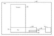
- the host 10may be a consumer electronic device, such as, a cell phone, a personal digital assistant (PDA), a handheld computer, game console, a personal computer (PC), or a notebook computer, for example.
- PDApersonal digital assistant
- PCpersonal computer
- notebook computerfor example.
- the host 10may have a processor 12 configured with a port 14 .
- the portis dedicated to communications with a data storage device, such as a fixed storage device 16 .
- the processor 12 and the fixed storage device 16communicate over a bus 18 via a controller 20 .
- the fixed storage device 16may be a non-volatile memory such as a flash memory device, such as a flash memory card, and may be capable of storing blocks of data.
- the processor 12may be configured with a number of ports to allow the host 10 to provide a variety of services to a user.
- the host 10may have ports dedicated to wireless communication antennas, video outputs, cameras, etc.
- the host 10may have a slot 22 into which a removable storage device 24 , such as a MMC, SD card, SDIO card, or MS card, for example, may be inserted.
- a removable storage device 24such as a MMC, SD card, SDIO card, or MS card, for example.
- the slot 22may be configured to receive a particular type or several different types of removable storage devices.
- the removable storage device 24 and the processormay communicate via the bus 18 .
- the controller 20may be configured to be compatible with the removable storage device 24 and the fixed storage device 16 .
- a standard initialization sequence 30is illustrated in FIG. 3 .
- the standard initialization sequence 30begins by powering up the storage device, as indicated at block 32 .
- a power up sequencemay include applying a particular voltage to the bus, setting a clock in the storage device, and determining an operating voltage level according to the particular specification for the storage device.
- the hostreceives an identification number corresponding to the storage device (e.g., in the case of a flash card, a CID) and provides a relative address, e.g. in the case of a flash card, a (RCA) assignment for the storage device, as indicated at block 34 .
- an identification number corresponding to the storage devicee.g., in the case of a flash card, a CID
- RCArelative address assignment for the storage device
- the host 10then receives storage device specific data (e.g., CSD) information that allows the host to know how to access the device and adjust host parameters accordingly, as indicated at block 36 .
- storage device specific datae.g., CSD
- all of the informationhas been communicated between the storage device and the host using a default bus width, e.g., x1.
- the initialization process 30continues by determining if the device is fixed, as indicated at decision block 37 . If the device is removable, the bus width is adjusted, as indicated at block 38 . Specifically, for example, the bus width is adjusted from the x1 bus width to a wider bus width (x4 or x8), if supported by both the host and the device.
- the bus width adjustmentcan include a number of steps including sending blocks of data to the device and receiving blocks of data back from all available data lines, as indicated at blocks 40 and 42 .
- the size of the received data blockmay be used by the host to determine the bus width supported by the device. For example, if eight bytes are received by the host, the device has eight available data lines.
- the received datamay then be masked with the data initially sent during bus width determination and resent to the device, as indicated at block 44 .
- all the datashould be zero. Any other result indicates an error and a recovery procedure is initiated, as indicated at block 46 .
- the hostmay select a bus width, as indicated at block 48 .
- the power classcan be adjusted, as indicated at block 50 . The power class adjustment is made based on the power requirements/capabilities of the device.
- the default power classprovides minimum current consumption for the card type. Generally, in the default power class 1.8V are supplied.
- devicesmay also be configured to operate in a high power class (supplying 3.3V) or a dual-power class, which supports both default power class (1.8V) and high power class (3.3V).
- a high power classsupplying 3.3V
- a dual-power classwhich supports both default power class (1.8V) and high power class (3.3V).
- the hostmay know the common bus width supported by fixed data storage device before initialization of the device begins and the initialization steps of blocks 38 - 48 are no longer needed, as indicated by decision block 37 and line 54 .
- One possible implementation for defining the wider data bus width of the fixed data storage device before initialization beginsis described below.
- a data storage controllercan be designed that supports both a standard initialization sequence and an abbreviated initialization sequence.
- the controller 20may have aspects of its hardware configured differently, such as by having two configurable bond pads: a first bond pad 56 for mode selection, and a second bond pad 58 for default data bus width.
- Each bond padmay be configured with a pull-up circuit internal to the controller so that if left floating (not bonded) the resulting state is a “1”. Alternatively, if the bond pad is tied to ground, the resulting state is a “0”.
- controller hardwareconfigures itself based on Table 1, shown below.
- the bond pads 56 and 58may be configured to allow for bus width determination steps to be carried out. For example, as set forth in Table 1, if the controller hardware detects that the mode section bond pad 56 is tied to ground (indicating one state), a standard initialization sequence requiring bus determination should be followed in accordance with conventional procedures, or alternative procedures described below.
- the bus negotiationallows for the host 10 to know the supported bus widths of the removable storage devices which may vary and may not be known in advance by the controller 20 .
- the data bus bond pad 58indicates the supported bus width, either x4 or x8. For example, as indicated in Table 1, if the data bus bond pad 58 indicates a 0 state, then a x4 bus is indicated and if the data bus bond pad 58 indicates a 1 state, a x8 bus is indicated. If, as illustrated in FIG. 1 , a fixed storage device 16 is provided, the bond pads can be configured to indicate the supported bus width of the fixed storage device in accordance with Table 1 because the supported bus width may be known when the fixed storage device is installed.
- the improved initialization sequenceincreases the efficiency of the initialization process by eliminating the bus width determination procedure and by eliminating switching from operating in a x1 bus configuration to a wider bus configuration.
- bus width negotiation schemesmay be implemented for bus width negotiation of removable storage devices.
- the bus width negotiationis performed by reading a bus width signal from a removable data storage device to determine the bus width of the removable data storage device. Once the bus width is determined, an enable signal is returned to the removable data storage device.
- FIG. 4illustrates an exemplary removable storage device 70 .
- the removable data storage devicehas a MMC form factor, but it should be understood that the techniques described herein may be applied to all types of removable data storage devices.
- bus width informationis multiplexed on to a pin used by the device for other functions, for example, pin 72 of the removable storage device 70 .
- the bus width determinationmay be performed during the “wake-up” clock cycles commonly provided by a host 10 prior to establishing communication with the removable storage device 50 . After the wake-up cycles are complete the multiplexed pin 72 is no longer used for bus width determination, and it returns to its normal function.
- an exemplary removable data storage device 80is configured to indicate an increased bus width using dedicated pins.
- MMC cardsgenerally only have 7 pins, as illustrated in FIG. 4 .
- the removable data storage device 80has additional pins 82 and 84 for indicating increased bus widths are supported by the device 80 . Since the pins 82 and 84 do not exist on removable data storage devices that only support a x1 bus width, the host 10 can determine whether increased bus widths are supported by simply sensing whether the pins 82 and/or 84 are present.
- pin 82may indicate x4 bus width support
- pin 84may indicate x8 bus width support.
- each of the extra pins 82 and 84may be set to a state (“1” or “0”) to indicate the ability of the device 80 to support a particular wider bus width, such as x4 or x8.
- the pinsmay be configured according to Table 1. It should be noted that the techniques described above, with reference to FIG. 5 , may be asynchronous, e.g. no clock signal is used.
- a dedicated pin 92is added to a removable data storage device 90 , as illustrated in FIG. 6 .
- the pin 92drives an output signal, such as a series of bits.
- the output signal of pin 92is sensed by the host 10 and used to determine the bus widths supported by the removable data storage device 90 . Having received the signal from the MMC, the host 10 determines the proper bus width to use with device 90 and returns a signal indicating the bus width to be used to pin 92 .
- the activity across the busis synchronous and a clock is sourced from the host 10 to the removable storage device 58 .
- a flow chart 100illustrates the bus width negotiation in accordance with an embodiment of the present invention.
- the configuration of the first bond padis determined, as indicated at block 102 .
- the first bond padmay be a mode pad indicating whether the system is configured to communicate with a fixed data storage device or a removable data storage device.
- the data storage deviceis fixed, as indicated at decision block 104 . If it is not fixed, then a bus width determination is performed, as indicated at block 106 .
- the bus width determinationmay include any of the above mentioned techniques, such as the standard technique, multiplexing information on an existing pin, or the addition of pins to the removable data storage device, for example.
- the configuration of the second bond padis determined, as indicated at block 108 .
- the second bond padindicates the supported bus width of the fixed data storage device, as discussed above. Once the host knows the supported bus width, as indicated by the second bond pad, data communication between the data storage device and the host may begin, as indicated at block 110 .
- the aforementioned methods and techniquesare performed before normal data communication is established between the host 10 and the removable storage device 24 .
- the host system 10can then configure its own data bus width hardware before sending any commands, thereby eliminating the need for initiating communications over a x1 bus and later switching to a different bus width.
- the sensing operationscan be handled using hardware in the host 10 , eliminating the need for the operating code to make decisions regarding bus width.
Landscapes
- Engineering & Computer Science (AREA)
- Theoretical Computer Science (AREA)
- Physics & Mathematics (AREA)
- General Engineering & Computer Science (AREA)
- General Physics & Mathematics (AREA)
- Information Transfer Systems (AREA)
- Techniques For Improving Reliability Of Storages (AREA)
Abstract
Description
| TABLE 1 | ||
| Mode | Data | |
| Selection | Bus | Result |
| 0 | 0 | Standard initialization sequence-requires |
| bus width determination procedure | ||
| 0 | 1 | Standard initialization sequence-requires |
| bus width determination procedure | ||
| 1 | 0 | Abbreviated initialization sequence-x4 data |
| bus predefined | ||
| 1 | 1 | Abbreviated initialization sequence-x8 data |
| bus predefined | ||
Claims (30)
Priority Applications (1)
| Application Number | Priority Date | Filing Date | Title |
|---|---|---|---|
| US13/009,559US9092388B2 (en) | 2007-06-27 | 2011-01-19 | Bus width negotiation |
Applications Claiming Priority (3)
| Application Number | Priority Date | Filing Date | Title |
|---|---|---|---|
| US11/823,262US7624211B2 (en) | 2007-06-27 | 2007-06-27 | Method for bus width negotiation of data storage devices |
| US12/619,528US7877530B2 (en) | 2007-06-27 | 2009-11-16 | Bus width negotiation |
| US13/009,559US9092388B2 (en) | 2007-06-27 | 2011-01-19 | Bus width negotiation |
Related Parent Applications (1)
| Application Number | Title | Priority Date | Filing Date |
|---|---|---|---|
| US12/619,528ContinuationUS7877530B2 (en) | 2007-06-27 | 2009-11-16 | Bus width negotiation |
Publications (2)
| Publication Number | Publication Date |
|---|---|
| US20110113163A1 US20110113163A1 (en) | 2011-05-12 |
| US9092388B2true US9092388B2 (en) | 2015-07-28 |
Family
ID=39687044
Family Applications (3)
| Application Number | Title | Priority Date | Filing Date |
|---|---|---|---|
| US11/823,262Active2028-02-19US7624211B2 (en) | 2007-06-27 | 2007-06-27 | Method for bus width negotiation of data storage devices |
| US12/619,528ActiveUS7877530B2 (en) | 2007-06-27 | 2009-11-16 | Bus width negotiation |
| US13/009,559Active2029-10-07US9092388B2 (en) | 2007-06-27 | 2011-01-19 | Bus width negotiation |
Family Applications Before (2)
| Application Number | Title | Priority Date | Filing Date |
|---|---|---|---|
| US11/823,262Active2028-02-19US7624211B2 (en) | 2007-06-27 | 2007-06-27 | Method for bus width negotiation of data storage devices |
| US12/619,528ActiveUS7877530B2 (en) | 2007-06-27 | 2009-11-16 | Bus width negotiation |
Country Status (3)
| Country | Link |
|---|---|
| US (3) | US7624211B2 (en) |
| TW (1) | TWI372976B (en) |
| WO (1) | WO2009002711A1 (en) |
Families Citing this family (9)
| Publication number | Priority date | Publication date | Assignee | Title |
|---|---|---|---|---|
| JP5244037B2 (en)* | 2008-07-15 | 2013-07-24 | パナソニック株式会社 | Memory device, memory device controller |
| US9280194B2 (en) | 2012-06-25 | 2016-03-08 | Intel Corporation | Dynamic link width modulation |
| US8904078B2 (en) | 2012-10-22 | 2014-12-02 | Lenovo Enterprise Solutions (Singapore) Pte. Ltd. | High speed serial peripheral interface system |
| US9892068B2 (en) | 2012-12-06 | 2018-02-13 | Rambus Inc. | Local internal discovery and configuration of individually selected and jointly selected devices |
| CN104981872B (en)* | 2013-03-15 | 2018-11-06 | 英特尔公司 | Storage system |
| US20150213850A1 (en)* | 2014-01-24 | 2015-07-30 | Qualcomm Incorporated | Serial data transmission for dynamic random access memory (dram) interfaces |
| US10163508B2 (en) | 2016-02-26 | 2018-12-25 | Intel Corporation | Supporting multiple memory types in a memory slot |
| US11467999B2 (en) | 2018-06-29 | 2022-10-11 | Intel Corporation | Negotiating asymmetric link widths dynamically in a multi-lane link |
| US11836101B2 (en)* | 2019-11-27 | 2023-12-05 | Intel Corporation | Partial link width states for bidirectional multilane links |
Citations (34)
| Publication number | Priority date | Publication date | Assignee | Title |
|---|---|---|---|---|
| US4987529A (en) | 1988-08-11 | 1991-01-22 | Ast Research, Inc. | Shared memory bus system for arbitrating access control among contending memory refresh circuits, peripheral controllers, and bus masters |
| US5025415A (en) | 1988-09-28 | 1991-06-18 | Fujitsu Limited | Memory card |
| US5119486A (en) | 1989-01-17 | 1992-06-02 | Prime Computer | Memory board selection method and apparatus |
| US5179542A (en) | 1991-12-31 | 1993-01-12 | Raytheon Company | Signal processor |
| US5448699A (en)* | 1990-12-21 | 1995-09-05 | Compaq Computer Corp. | Apparatus with leading edge delay circuit for selectively sending a delayed substitute version of a signal transmitted between an expansion card and a system bus |
| US5600801A (en) | 1993-07-15 | 1997-02-04 | Dell Usa, L.P. | Multiple function interface device for option card |
| US5613078A (en) | 1992-11-09 | 1997-03-18 | Kabushiki Kaisha Toshiba | Microprocessor and microprocessor system with changeable effective bus width |
| WO1997045870A1 (en)* | 1996-05-24 | 1997-12-04 | Microchip Technology, Inc. | A microcontroller having an n-bit data bus width with less than n i/o pins and a method therefor |
| WO1999021127A1 (en)* | 1997-10-17 | 1999-04-29 | I-O Data Device Inc. | Card-shaped medium and pc card |
| US5906003A (en)* | 1996-04-17 | 1999-05-18 | Cirrus Logic, Inc. | Memory device with an externally selectable-width I/O port and systems and methods using the same |
| US6246228B1 (en)* | 1998-11-27 | 2001-06-12 | The United States Of America As Represented By The Administrator Of The National Aeronautics And Space Administration | Non-contact linear actuator position sensor having a pid-compensating controller |
| US6438638B1 (en)* | 2000-07-06 | 2002-08-20 | Onspec Electronic, Inc. | Flashtoaster for reading several types of flash-memory cards with or without a PC |
| US20030056050A1 (en) | 2001-09-14 | 2003-03-20 | Kabushiki Kaisha Toshiba | Card device |
| US20040107327A1 (en) | 2002-08-14 | 2004-06-03 | Toshio Takahashi | Method and circuit for interfacing card memory, asic embedded with the interface circuit, and image forming apparatus equipped with the asic |
| US20040137805A1 (en) | 2002-11-29 | 2004-07-15 | Nokia Corporation | Method and a system for detecting bus width, an electronic device, and a peripheral device |
| US6825845B2 (en)* | 2002-03-28 | 2004-11-30 | Texas Instruments Incorporated | Virtual frame buffer control system |
| US20050005209A1 (en) | 2003-07-02 | 2005-01-06 | Nokia Corporation | Memory bus checking procedure |
| US6842840B1 (en) | 2001-02-27 | 2005-01-11 | Intel Corporation | Controller which determines presence of memory in a node of a data network |
| US6857038B2 (en)* | 2002-06-07 | 2005-02-15 | Wen-Tsung Liu | Common connector for memory cards and switching arbitration method for shared pins of a connector |
| US6901457B1 (en) | 1998-11-04 | 2005-05-31 | Sandisk Corporation | Multiple mode communications system |
| US6906961B2 (en) | 2003-06-24 | 2005-06-14 | Micron Technology, Inc. | Erase block data splitting |
| WO2005076143A1 (en) | 2004-02-05 | 2005-08-18 | Research In Motion Limited | System and method for detecting the width of a data bus |
| US20050193170A1 (en) | 2004-02-27 | 2005-09-01 | Brother Kogyo Kabushiki Kaisha | Electronic apparatus and method for detecting a state of a removable medium |
| US20050204091A1 (en) | 2004-03-11 | 2005-09-15 | Kilbuck Kevin M. | Non-volatile memory with synchronous DRAM interface |
| US20050211786A1 (en) | 2003-02-07 | 2005-09-29 | Renesas Technology Corp. | Nonvolatile memory |
| US7009846B1 (en) | 2004-07-30 | 2006-03-07 | Super Talent Electronics, Inc. | 13-Pin socket for combination SD/MMC flash memory system |
| US7069369B2 (en)* | 2004-02-12 | 2006-06-27 | Super Talent Electronics, Inc. | Extended-Secure-Digital interface using a second protocol for faster transfers |
| US7085875B1 (en) | 2000-04-06 | 2006-08-01 | Avaya Communication Israel Ltd. | Modular switch with dynamic bus |
| US20070061672A1 (en) | 2005-09-01 | 2007-03-15 | David Eggleston | Non-volatile memory with error detection |
| US20070088940A1 (en) | 2005-10-13 | 2007-04-19 | Sandisk Corporation | Initialization of flash storage via an embedded controller |
| US7234031B2 (en)* | 2003-06-21 | 2007-06-19 | Samsung Electronics Co., Ltd. | Portable storage apparatus and method for freely changing data bus width |
| US7343577B2 (en)* | 2005-09-13 | 2008-03-11 | Alcatel | Area array routing masks for improved escape of devices on PCB |
| US7457942B2 (en) | 2002-09-17 | 2008-11-25 | Ricoh Company, Ltd. | PC card control device, computer system using the PC card control device, and PC card identifying method |
| US7610417B2 (en)* | 2005-11-30 | 2009-10-27 | Rambus Inc. | Data-width translator coupled between variable-width and fixed-width data ports and supporting multiple data-width configurations |
Family Cites Families (9)
| Publication number | Priority date | Publication date | Assignee | Title |
|---|---|---|---|---|
| US5317707A (en)* | 1989-10-20 | 1994-05-31 | Texas Instruments Incorporated | Expanded memory interface for supporting expanded, conventional or extended memory for communication between an application processor and an external processor |
| US5663901A (en)* | 1991-04-11 | 1997-09-02 | Sandisk Corporation | Computer memory cards using flash EEPROM integrated circuit chips and memory-controller systems |
| JPH05274282A (en)* | 1992-03-30 | 1993-10-22 | Canon Inc | Method for information processing and device therefor |
| US5721860A (en)* | 1994-05-24 | 1998-02-24 | Intel Corporation | Memory controller for independently supporting synchronous and asynchronous DRAM memories |
| US6567904B1 (en)* | 1995-12-29 | 2003-05-20 | Intel Corporation | Method and apparatus for automatically detecting whether a memory unit location is unpopulated or populated with synchronous or asynchronous memory devices |
| US6148347A (en)* | 1996-11-20 | 2000-11-14 | Cisco Technology, Inc. | Mode selectable memory controller for PCMCIA standard memory cards and non-standard memory cards |
| US7367503B2 (en)* | 2002-11-13 | 2008-05-06 | Sandisk Corporation | Universal non-volatile memory card used with various different standard cards containing a memory controller |
| US6938104B2 (en)* | 2003-08-12 | 2005-08-30 | Arco Computer Products, Inc. | Removable hard drive assembly, computer with a removable hard disk drive, method of initializing and operating a removable hard drive |
| US7321524B2 (en)* | 2005-10-17 | 2008-01-22 | Rambus Inc. | Memory controller with staggered request signal output |
- 2007
- 2007-06-27USUS11/823,262patent/US7624211B2/enactiveActive
- 2008
- 2008-06-12WOPCT/US2008/066642patent/WO2009002711A1/enactiveApplication Filing
- 2008-06-27TWTW097124387Apatent/TWI372976B/enactive
- 2009
- 2009-11-16USUS12/619,528patent/US7877530B2/enactiveActive
- 2011
- 2011-01-19USUS13/009,559patent/US9092388B2/enactiveActive
Patent Citations (41)
| Publication number | Priority date | Publication date | Assignee | Title |
|---|---|---|---|---|
| US4987529A (en) | 1988-08-11 | 1991-01-22 | Ast Research, Inc. | Shared memory bus system for arbitrating access control among contending memory refresh circuits, peripheral controllers, and bus masters |
| US5025415A (en) | 1988-09-28 | 1991-06-18 | Fujitsu Limited | Memory card |
| US5119486A (en) | 1989-01-17 | 1992-06-02 | Prime Computer | Memory board selection method and apparatus |
| US5448699A (en)* | 1990-12-21 | 1995-09-05 | Compaq Computer Corp. | Apparatus with leading edge delay circuit for selectively sending a delayed substitute version of a signal transmitted between an expansion card and a system bus |
| US5179542A (en) | 1991-12-31 | 1993-01-12 | Raytheon Company | Signal processor |
| US5613078A (en) | 1992-11-09 | 1997-03-18 | Kabushiki Kaisha Toshiba | Microprocessor and microprocessor system with changeable effective bus width |
| US5600801A (en) | 1993-07-15 | 1997-02-04 | Dell Usa, L.P. | Multiple function interface device for option card |
| US5906003A (en)* | 1996-04-17 | 1999-05-18 | Cirrus Logic, Inc. | Memory device with an externally selectable-width I/O port and systems and methods using the same |
| US5847450A (en)* | 1996-05-24 | 1998-12-08 | Microchip Technology Incorporated | Microcontroller having an n-bit data bus width with less than n I/O pins |
| WO1997045870A1 (en)* | 1996-05-24 | 1997-12-04 | Microchip Technology, Inc. | A microcontroller having an n-bit data bus width with less than n i/o pins and a method therefor |
| WO1999021127A1 (en)* | 1997-10-17 | 1999-04-29 | I-O Data Device Inc. | Card-shaped medium and pc card |
| US6481629B1 (en) | 1997-10-17 | 2002-11-19 | I-O Data Device, Inc. | PC card with variable width data bus communication capabilities |
| US6901457B1 (en) | 1998-11-04 | 2005-05-31 | Sandisk Corporation | Multiple mode communications system |
| US6246228B1 (en)* | 1998-11-27 | 2001-06-12 | The United States Of America As Represented By The Administrator Of The National Aeronautics And Space Administration | Non-contact linear actuator position sensor having a pid-compensating controller |
| US7085875B1 (en) | 2000-04-06 | 2006-08-01 | Avaya Communication Israel Ltd. | Modular switch with dynamic bus |
| US6438638B1 (en)* | 2000-07-06 | 2002-08-20 | Onspec Electronic, Inc. | Flashtoaster for reading several types of flash-memory cards with or without a PC |
| US6842840B1 (en) | 2001-02-27 | 2005-01-11 | Intel Corporation | Controller which determines presence of memory in a node of a data network |
| US20030056050A1 (en) | 2001-09-14 | 2003-03-20 | Kabushiki Kaisha Toshiba | Card device |
| US6825845B2 (en)* | 2002-03-28 | 2004-11-30 | Texas Instruments Incorporated | Virtual frame buffer control system |
| US6857038B2 (en)* | 2002-06-07 | 2005-02-15 | Wen-Tsung Liu | Common connector for memory cards and switching arbitration method for shared pins of a connector |
| US20040107327A1 (en) | 2002-08-14 | 2004-06-03 | Toshio Takahashi | Method and circuit for interfacing card memory, asic embedded with the interface circuit, and image forming apparatus equipped with the asic |
| US7457942B2 (en) | 2002-09-17 | 2008-11-25 | Ricoh Company, Ltd. | PC card control device, computer system using the PC card control device, and PC card identifying method |
| US20040137805A1 (en) | 2002-11-29 | 2004-07-15 | Nokia Corporation | Method and a system for detecting bus width, an electronic device, and a peripheral device |
| US20050211786A1 (en) | 2003-02-07 | 2005-09-29 | Renesas Technology Corp. | Nonvolatile memory |
| US6972979B2 (en) | 2003-02-07 | 2005-12-06 | Renesas Technology Corp. | Nonvolatile memory |
| US7234031B2 (en)* | 2003-06-21 | 2007-06-19 | Samsung Electronics Co., Ltd. | Portable storage apparatus and method for freely changing data bus width |
| US6906961B2 (en) | 2003-06-24 | 2005-06-14 | Micron Technology, Inc. | Erase block data splitting |
| US20050190599A1 (en) | 2003-06-24 | 2005-09-01 | Micron Technology, Inc. | Erase block data splitting |
| US7193899B2 (en) | 2003-06-24 | 2007-03-20 | Micron Technology, Inc. | Erase block data splitting |
| US20060256624A1 (en) | 2003-06-24 | 2006-11-16 | Micron Technology, Inc. | Erase block data splitting |
| US7036054B2 (en) | 2003-07-02 | 2006-04-25 | Nokia Corporation | Memory bus checking procedure |
| US20050005209A1 (en) | 2003-07-02 | 2005-01-06 | Nokia Corporation | Memory bus checking procedure |
| WO2005076143A1 (en) | 2004-02-05 | 2005-08-18 | Research In Motion Limited | System and method for detecting the width of a data bus |
| US7069369B2 (en)* | 2004-02-12 | 2006-06-27 | Super Talent Electronics, Inc. | Extended-Secure-Digital interface using a second protocol for faster transfers |
| US20050193170A1 (en) | 2004-02-27 | 2005-09-01 | Brother Kogyo Kabushiki Kaisha | Electronic apparatus and method for detecting a state of a removable medium |
| US20050204091A1 (en) | 2004-03-11 | 2005-09-15 | Kilbuck Kevin M. | Non-volatile memory with synchronous DRAM interface |
| US7009846B1 (en) | 2004-07-30 | 2006-03-07 | Super Talent Electronics, Inc. | 13-Pin socket for combination SD/MMC flash memory system |
| US20070061672A1 (en) | 2005-09-01 | 2007-03-15 | David Eggleston | Non-volatile memory with error detection |
| US7343577B2 (en)* | 2005-09-13 | 2008-03-11 | Alcatel | Area array routing masks for improved escape of devices on PCB |
| US20070088940A1 (en) | 2005-10-13 | 2007-04-19 | Sandisk Corporation | Initialization of flash storage via an embedded controller |
| US7610417B2 (en)* | 2005-11-30 | 2009-10-27 | Rambus Inc. | Data-width translator coupled between variable-width and fixed-width data ports and supporting multiple data-width configurations |
Non-Patent Citations (3)
| Title |
|---|
| "SDIO Card Specification," Oct. 2001, SD Association, Hollister, CA, USA, XP002493459. |
| Invitation to Pay Additional Fees and, Where Applicable, Protest Fee; European Patent Office, Sep. 9, 2008. |
| MMC Specification Version 1.3 Jul. 8, 2004.* |
Also Published As
| Publication number | Publication date |
|---|---|
| US20090006691A1 (en) | 2009-01-01 |
| TW200917040A (en) | 2009-04-16 |
| TWI372976B (en) | 2012-09-21 |
| US20110113163A1 (en) | 2011-05-12 |
| US7624211B2 (en) | 2009-11-24 |
| US20100064089A1 (en) | 2010-03-11 |
| WO2009002711A1 (en) | 2008-12-31 |
| US7877530B2 (en) | 2011-01-25 |
Similar Documents
| Publication | Publication Date | Title |
|---|---|---|
| US9092388B2 (en) | Bus width negotiation | |
| US11922022B2 (en) | Method for transferring data on a memory card in synchronism with a rise edge and a fall edge of a clock signal | |
| US12287694B2 (en) | Card and host apparatus | |
| US7934037B2 (en) | Extended Secure-Digital (SD) devices and hosts | |
| US6901457B1 (en) | Multiple mode communications system | |
| US20050038956A1 (en) | Method and an apparatus of flash cards access | |
| JP2006518897A (en) | Multi-protocol memory card | |
| US20040064612A1 (en) | Method and system for using a memory card protocol inside a bus protocol | |
| EP3905055B1 (en) | Link startup method of storage device, and storage device, host and system implementing same | |
| US8883521B2 (en) | Control method of multi-chip package memory device | |
| EP1763036B1 (en) | Semiconductor storage device, electronic apparatus, and mode setting method | |
| JP2007299377A (en) | Multi-micro memory card, and its interface change detection method | |
| US11755439B2 (en) | Memory controller, test device and link identification method | |
| US7275186B2 (en) | Memory bus checking procedure | |
| JP5928715B2 (en) | IC card | |
| CN111918277A (en) | Data storage management |
Legal Events
| Date | Code | Title | Description |
|---|---|---|---|
| FEPP | Fee payment procedure | Free format text:PAYOR NUMBER ASSIGNED (ORIGINAL EVENT CODE: ASPN); ENTITY STATUS OF PATENT OWNER: LARGE ENTITY | |
| STCF | Information on status: patent grant | Free format text:PATENTED CASE | |
| AS | Assignment | Owner name:U.S. BANK NATIONAL ASSOCIATION, AS COLLATERAL AGENT, CALIFORNIA Free format text:SECURITY INTEREST;ASSIGNOR:MICRON TECHNOLOGY, INC.;REEL/FRAME:038669/0001 Effective date:20160426 Owner name:U.S. BANK NATIONAL ASSOCIATION, AS COLLATERAL AGEN Free format text:SECURITY INTEREST;ASSIGNOR:MICRON TECHNOLOGY, INC.;REEL/FRAME:038669/0001 Effective date:20160426 | |
| AS | Assignment | Owner name:MORGAN STANLEY SENIOR FUNDING, INC., AS COLLATERAL AGENT, MARYLAND Free format text:PATENT SECURITY AGREEMENT;ASSIGNOR:MICRON TECHNOLOGY, INC.;REEL/FRAME:038954/0001 Effective date:20160426 Owner name:MORGAN STANLEY SENIOR FUNDING, INC., AS COLLATERAL Free format text:PATENT SECURITY AGREEMENT;ASSIGNOR:MICRON TECHNOLOGY, INC.;REEL/FRAME:038954/0001 Effective date:20160426 | |
| AS | Assignment | Owner name:U.S. BANK NATIONAL ASSOCIATION, AS COLLATERAL AGENT, CALIFORNIA Free format text:CORRECTIVE ASSIGNMENT TO CORRECT THE REPLACE ERRONEOUSLY FILED PATENT #7358718 WITH THE CORRECT PATENT #7358178 PREVIOUSLY RECORDED ON REEL 038669 FRAME 0001. ASSIGNOR(S) HEREBY CONFIRMS THE SECURITY INTEREST;ASSIGNOR:MICRON TECHNOLOGY, INC.;REEL/FRAME:043079/0001 Effective date:20160426 Owner name:U.S. BANK NATIONAL ASSOCIATION, AS COLLATERAL AGEN Free format text:CORRECTIVE ASSIGNMENT TO CORRECT THE REPLACE ERRONEOUSLY FILED PATENT #7358718 WITH THE CORRECT PATENT #7358178 PREVIOUSLY RECORDED ON REEL 038669 FRAME 0001. ASSIGNOR(S) HEREBY CONFIRMS THE SECURITY INTEREST;ASSIGNOR:MICRON TECHNOLOGY, INC.;REEL/FRAME:043079/0001 Effective date:20160426 | |
| AS | Assignment | Owner name:JPMORGAN CHASE BANK, N.A., AS COLLATERAL AGENT, ILLINOIS Free format text:SECURITY INTEREST;ASSIGNORS:MICRON TECHNOLOGY, INC.;MICRON SEMICONDUCTOR PRODUCTS, INC.;REEL/FRAME:047540/0001 Effective date:20180703 Owner name:JPMORGAN CHASE BANK, N.A., AS COLLATERAL AGENT, IL Free format text:SECURITY INTEREST;ASSIGNORS:MICRON TECHNOLOGY, INC.;MICRON SEMICONDUCTOR PRODUCTS, INC.;REEL/FRAME:047540/0001 Effective date:20180703 | |
| AS | Assignment | Owner name:MICRON TECHNOLOGY, INC., IDAHO Free format text:RELEASE BY SECURED PARTY;ASSIGNOR:U.S. BANK NATIONAL ASSOCIATION, AS COLLATERAL AGENT;REEL/FRAME:047243/0001 Effective date:20180629 | |
| MAFP | Maintenance fee payment | Free format text:PAYMENT OF MAINTENANCE FEE, 4TH YEAR, LARGE ENTITY (ORIGINAL EVENT CODE: M1551); ENTITY STATUS OF PATENT OWNER: LARGE ENTITY Year of fee payment:4 | |
| AS | Assignment | Owner name:MICRON TECHNOLOGY, INC., IDAHO Free format text:RELEASE BY SECURED PARTY;ASSIGNOR:MORGAN STANLEY SENIOR FUNDING, INC., AS COLLATERAL AGENT;REEL/FRAME:050937/0001 Effective date:20190731 | |
| AS | Assignment | Owner name:MICRON TECHNOLOGY, INC., IDAHO Free format text:RELEASE BY SECURED PARTY;ASSIGNOR:JPMORGAN CHASE BANK, N.A., AS COLLATERAL AGENT;REEL/FRAME:051028/0001 Effective date:20190731 Owner name:MICRON SEMICONDUCTOR PRODUCTS, INC., IDAHO Free format text:RELEASE BY SECURED PARTY;ASSIGNOR:JPMORGAN CHASE BANK, N.A., AS COLLATERAL AGENT;REEL/FRAME:051028/0001 Effective date:20190731 | |
| MAFP | Maintenance fee payment | Free format text:PAYMENT OF MAINTENANCE FEE, 8TH YEAR, LARGE ENTITY (ORIGINAL EVENT CODE: M1552); ENTITY STATUS OF PATENT OWNER: LARGE ENTITY Year of fee payment:8 |