US9091935B2 - Multistage extreme ultra-violet mask qualification - Google Patents
Multistage extreme ultra-violet mask qualificationDownload PDFInfo
- Publication number
- US9091935B2 US9091935B2US13/794,330US201313794330AUS9091935B2US 9091935 B2US9091935 B2US 9091935B2US 201313794330 AUS201313794330 AUS 201313794330AUS 9091935 B2US9091935 B2US 9091935B2
- Authority
- US
- United States
- Prior art keywords
- image
- mask
- potential defects
- photo
- euv
- Prior art date
- Legal status (The legal status is an assumption and is not a legal conclusion. Google has not performed a legal analysis and makes no representation as to the accuracy of the status listed.)
- Active, expires
Links
Images


Classifications
- G—PHYSICS
- G03—PHOTOGRAPHY; CINEMATOGRAPHY; ANALOGOUS TECHNIQUES USING WAVES OTHER THAN OPTICAL WAVES; ELECTROGRAPHY; HOLOGRAPHY
- G03F—PHOTOMECHANICAL PRODUCTION OF TEXTURED OR PATTERNED SURFACES, e.g. FOR PRINTING, FOR PROCESSING OF SEMICONDUCTOR DEVICES; MATERIALS THEREFOR; ORIGINALS THEREFOR; APPARATUS SPECIALLY ADAPTED THEREFOR
- G03F1/00—Originals for photomechanical production of textured or patterned surfaces, e.g., masks, photo-masks, reticles; Mask blanks or pellicles therefor; Containers specially adapted therefor; Preparation thereof
- G03F1/68—Preparation processes not covered by groups G03F1/20 - G03F1/50
- G03F1/70—Adapting basic layout or design of masks to lithographic process requirements, e.g., second iteration correction of mask patterns for imaging
- G—PHYSICS
- G06—COMPUTING OR CALCULATING; COUNTING
- G06T—IMAGE DATA PROCESSING OR GENERATION, IN GENERAL
- G06T7/00—Image analysis
- G06T7/0002—Inspection of images, e.g. flaw detection
- G06T7/0004—Industrial image inspection
- G06T7/001—Industrial image inspection using an image reference approach
- G—PHYSICS
- G03—PHOTOGRAPHY; CINEMATOGRAPHY; ANALOGOUS TECHNIQUES USING WAVES OTHER THAN OPTICAL WAVES; ELECTROGRAPHY; HOLOGRAPHY
- G03F—PHOTOMECHANICAL PRODUCTION OF TEXTURED OR PATTERNED SURFACES, e.g. FOR PRINTING, FOR PROCESSING OF SEMICONDUCTOR DEVICES; MATERIALS THEREFOR; ORIGINALS THEREFOR; APPARATUS SPECIALLY ADAPTED THEREFOR
- G03F1/00—Originals for photomechanical production of textured or patterned surfaces, e.g., masks, photo-masks, reticles; Mask blanks or pellicles therefor; Containers specially adapted therefor; Preparation thereof
- G03F1/22—Masks or mask blanks for imaging by radiation of 100nm or shorter wavelength, e.g. X-ray masks, extreme ultraviolet [EUV] masks; Preparation thereof
- G03F1/24—Reflection masks; Preparation thereof
- G—PHYSICS
- G03—PHOTOGRAPHY; CINEMATOGRAPHY; ANALOGOUS TECHNIQUES USING WAVES OTHER THAN OPTICAL WAVES; ELECTROGRAPHY; HOLOGRAPHY
- G03F—PHOTOMECHANICAL PRODUCTION OF TEXTURED OR PATTERNED SURFACES, e.g. FOR PRINTING, FOR PROCESSING OF SEMICONDUCTOR DEVICES; MATERIALS THEREFOR; ORIGINALS THEREFOR; APPARATUS SPECIALLY ADAPTED THEREFOR
- G03F1/00—Originals for photomechanical production of textured or patterned surfaces, e.g., masks, photo-masks, reticles; Mask blanks or pellicles therefor; Containers specially adapted therefor; Preparation thereof
- G03F1/68—Preparation processes not covered by groups G03F1/20 - G03F1/50
- G03F1/82—Auxiliary processes, e.g. cleaning or inspecting
- G03F1/84—Inspecting
- G—PHYSICS
- G06—COMPUTING OR CALCULATING; COUNTING
- G06T—IMAGE DATA PROCESSING OR GENERATION, IN GENERAL
- G06T2207/00—Indexing scheme for image analysis or image enhancement
- G06T2207/10—Image acquisition modality
- G06T2207/10056—Microscopic image
- G—PHYSICS
- G06—COMPUTING OR CALCULATING; COUNTING
- G06T—IMAGE DATA PROCESSING OR GENERATION, IN GENERAL
- G06T2207/00—Indexing scheme for image analysis or image enhancement
- G06T2207/30—Subject of image; Context of image processing
- G06T2207/30108—Industrial image inspection
- G06T2207/30148—Semiconductor; IC; Wafer
Definitions
- the present inventionrelates to techniques for inspecting, qualifying and repairing a photo-mask for use in photolithography at extreme ultra-violet wavelengths.
- Photolithographyis a widely used technology for producing integrated circuits.
- a light sourceilluminates a photo-mask.
- the resulting spatially varying light patternis projected onto a photoresist layer on a semiconductor wafer by an optical system (which is referred to as an ‘exposure tool’).
- an optical systemwhich is referred to as an ‘exposure tool’.
- 3D3-dimensional
- EUV photo-maskshave been investigated for use with wavelengths in the extreme ultra-violet.
- a multilayer stackis used to reflect the light from the light source. For example, multiple alternating layers of silicon and molybdenum may be deposited on silicon or a glass substrate having an ultra-low thermal expansion coefficient (such as quartz). Then, the mask pattern may be defined in an absorption layer (such as tantalum nitride) that is deposited on top of the multilayer stack.
- an absorption layersuch as tantalum nitride
- this structurecan be difficult to manufacture. For example, during the manufacturing process defects can occur throughout the multilayer stack. It can be difficult to detect the presence of a defect in the multilayer stack without performing destructive analysis. In addition, even if a defect is detected (or when a type of defect is probable in a given manufacturing process), it is often difficult (or impossible) to predict the consequences of the defect in the photolithographic process (e.g., will the defect result in an unacceptable change in the 3D pattern) or to determine how to modify an EUV photo-mask to reduce or eliminate the effect of a defect on the photolithographic process.
- the inspection and qualification criteria for EUV photo-masksare often needlessly conservative, which results in rejection of EUV photo-masks that could be successfully used in the photolithographic process (i.e., the EUV photo-mask yield may be needlessly reduced), thereby significantly increasing the cost of EUV photo-masks.
- the present disclosurerelates to a computer system for determining a qualification condition of an extreme ultra-violet (EUV) photo-mask.
- EUVextreme ultra-violet
- the computer systemmeasures a first image of a substrate and a second image of a blank that includes multiple layers deposited on the substrate. Then, the computer system identifies first potential defects on the substrate and/or in the multiple layers based on the first image and the second image. Moreover, the computer system measures a third image of the EUV photo-mask that includes a mask pattern defined in an absorption layer, which is deposited on top of the multiple layers, wherein measurement of the third image uses information associated with the first potential defects. Next, the computer system identifies second potential defects in the EUV photo-mask based on the third image and the first potential defects. Based on the first potential defects and the second potential defects, the computer system determines the qualification condition of the EUV photo-mask.
- EUVextreme ultra-violet
- the second imagemay include: multiple optical microscope images that are obtained using different focal lengths or light polarizations; multiple confocal microscope images; an aerial image associated with the blank; and/or an image of a test-wafer pattern produced using the blank.
- measurement of the third imagemay involve alignment with the first image and the second image based on the information associated with the first potential defects, where the information may include masking of at least some of the first potential defects in the third image by the absorption layer.
- the informationmay include locations of the first potential defects.
- qualifying the EUV photo-maskmay involve a forward optical calculation to assess printability of the first potential defects and the second potential defects on a semiconductor wafer at an image plane of a model of an optical system associated with a photo-lithographic process.
- the computer systemdetermines a modification to the EUV photo-mask based on the first potential defects and the second potential defects.
- This modificationmay involve a change in the mask pattern.
- the modificationmay involve an additive process and/or a subtractive process.
- Another embodimentprovides a method including at least some of the above-described operations.
- Another embodimentprovides a computer-program product for use in conjunction with the computer system.
- FIG. 1is a flow chart illustrating a method for determining a qualification condition of an extreme ultra-violet (EUV) photo-mask in accordance with an embodiment of the present invention.
- EUVextreme ultra-violet
- FIG. 2is a drawing illustrating a side view of a multilayer stack in an EUV photo-mask in accordance with an embodiment of the present invention.
- FIG. 3is a drawing illustrating an inspection and repair process for an EUV photo-mask in accordance with an embodiment of the present invention.
- FIG. 4is a drawing illustrating multilayer defect reconstruction during the inspection and repair process in FIG. 3 in accordance with an embodiment of the present invention.
- FIG. 5is a drawing illustrating mask-pattern inspection during the inspection and repair process in FIG. 3 in accordance with an embodiment of the present invention.
- FIG. 6is a drawing illustrating coordinate constrained multi-image matching during the inspection and repair process in FIG. 3 in accordance with an embodiment of the present invention.
- FIG. 7is a drawing illustrating a defect-printing simulation during the inspection and repair process in FIG. 3 in accordance with an embodiment of the present invention.
- FIG. 8is a drawing illustrating a defect-printing simulation during the inspection and repair process in FIG. 3 in accordance with an embodiment of the present invention.
- FIG. 9is a block diagram illustrating a forward optical calculation in accordance with an embodiment of the present invention.
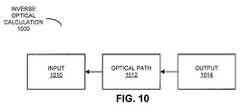
- FIG. 10is a block diagram illustrating an inverse optical calculation in accordance with an embodiment of the present invention.
- FIG. 11is a block diagram illustrating a computer system in accordance with an embodiment of the present invention.
- Embodiments of a computer system, a method, and a computer program product (i.e., software) for use with the computer systemare described. These systems and processes may be used to inspect, qualify and repair photo-masks for use at extreme ultra-violet (EUV) wavelengths, such as wavelengths between 10-124 nm.
- EUVextreme ultra-violet
- the computer systemidentifies first potential defects on the substrate and/or in the multiple layers.
- the computer systemmeasures a third image of the EUV photo-mask that includes a mask pattern defined in an absorption layer, which is deposited on top of the multiple layers. This measurement of the third image uses information associated with the first potential defects, such as locations of the first potential defects.
- the computer systemBased on the third image and the first potential defects, the computer system identifies second potential defects in the EUV photo-mask.
- the computer systemdetermines a qualification condition of the EUV photo-mask based on the first potential defects and the second potential defects.
- a reflective photo-mask(which is sometimes referred to as an ‘EUV photo-mask’) should be understood to include an absorption layer, an alternating phase-shift layer, and/or an attenuating phase-shift layer deposited on a multilayer stack, which in turn is deposited on a substrate.
- This reflective photo-maskmay be used in extreme ultra-violet photolithography.
- the reflective photo-maskmay be used in multiple-exposure photolithography, where patterns printed on a wafer or semiconductor die using two or more reflective photo-masks are combined to produce a desired or target pattern, such as a portion of an integrated circuit.
- a mask patternshould be understood to include the pattern of spatially varying transmittance magnitude and/or transmittance phase of the absorption layer, the alternating phase-shift layer, and/or the attenuating phase-shift layer deposited on the multilayer stack.
- the manufactured or fabricated mask pattern in a given reflective photo-maskmay deviate from an ideal target mask pattern, for example, because of defects that can occur during the photo-mask fabrication process.
- a mask pattern or a target patternmay include a bitmap or grayscale file that includes a set of values corresponding to pixels in the mask pattern or the target pattern.
- the quantizationi.e., the number of bits
- Alternative formats having the same or similar information contentincluding a vector-based format such as a Graphic Design System II (GDSII) and/or an OASIS format, may be used in some embodiments of the mask pattern or the target pattern.
- the mask pattern or the target patterninclude real and imaginary components (or equivalently, magnitude and phase information).
- FIG. 1presents a flow chart illustrating a method 100 for determining a qualification condition of an extreme ultra-violet (EUV) photo-mask, which may be performed by a computer system (such as computer system 1100 in FIG. 11 ).
- the computer systemmeasures a first image of a substrate and a second image of a blank that includes multiple layers deposited on (or disposed on) the substrate (operation 110 ).
- the first imagemay include: an aerial image of the substrate, a confocal microscope image of the substrate, a dark-field optical image, and/or an image of a test wafer pattern produced using the substrate.
- the second imagemay include: multiple optical microscope images that are obtained using different focal lengths or light polarizations; multiple confocal microscope images; an aerial image associated with the blank; and/or an image of a test wafer pattern produced using the blank.
- the computer systemidentifies first potential defects on the substrate and/or in the multiple layers based on the first image and the second image (operation 112 ).
- identifying the first potential defectsinvolves a first inverse optical calculation based on the first image and a second inverse optical calculation based on the second image, where the first image is at an image plane of a first model of a first optical system in the first inverse optical calculation and the second image is at the image plane of a second model of a second optical system in the second inverse optical calculation.
- the first model of the optical systemmay correspond to a first measurement system that measured the first image
- the second model of the optical systemmay correspond to a second measurement system that measured the second image.
- the computer systemmeasures a third image of the EUV photo-mask that includes a mask pattern defined in an absorption layer (operation 114 ), which is deposited on top of the multiple layers, wherein measurement of the third image uses information associated with the first potential defects.
- measurement of the third imagemay involve alignment with the first image and the second image based on the information associated with the first potential defects, where the information may include masking of at least some of the first potential defects in the third image by the absorption layer.
- the informationmay include locations of the first potential defects.
- the computer systemidentifies second potential defects in the EUV photo-mask based on the third image and the first potential defects (operation 116 ). Based on the first potential defects and the second potential defects, the computer system determines the qualification condition of the EUV photo-mask (operation 118 ).
- qualifying the EUV photo-maskmay involve a forward optical calculation to assess printability of the first potential defects and the second potential defects on a semiconductor wafer at an image plane of a model of an optical system associated with a photo-lithographic process. For example, a resist pattern on a wafer fabricated in a photo-lithographic process that uses the EUV photo-mask may be estimated. Forward optical calculations are described further below with reference to FIG. 9 .
- the computer systemoptionally determines a modification to the EUV photo-mask based on the first potential defects and the second potential defects (operation 120 ).
- This modificationmay involve a change in the mask pattern.
- the modificationmay involve an additive process (such as depositing another layer or an additional material on the photo-mask) and/or a subtractive process (such as etching).
- the computer systemmay optionally provide a remedial action based on the determined qualification condition.
- the computer systemmay provide instructions or suggestions as to how to repair or rework the EUV photo-mask.
- the mask patternmay be modified or another may be added so that the deviations in the critical dimension of the estimated resist pattern on the wafer fabricated using the EUV photo-mask are less than 10% relative to the critical dimension of a target pattern.
- the order of the operationsis changed, and two or more operations are combined into a single operation.
- the second imagemay include multiple images that are obtained at different focal lengths and/or different polarizations.
- the first image, the second image and/or the third imagemay be aligned during method 100 using fiducial markers on the substrate, the multilayer stack and/or an absorption layer of the EUV photo-mask.
- the computer systemmay receive one or more of these images from a separate source, such as a separate measurement device or system, or a third party that performs the measurements on the EUV photo-mask.
- the accuracy of identifying the first potential defectsmay be improved by using the first image and the second image.
- the second imageis used to identify the first potential defects.
- defects in the EUV photo-maskcan be identified and the performance of the EUV photo-mask may be appropriately assessed to determine the qualification condition.
- FIG. 2presents a drawing illustrating a side view of a multilayer stack 212 in a reflective (EUV) photo-mask 200 .
- multilayer stack 212may be deposited on a substrate 210 (such as silicon or quartz).
- substrate 210such as silicon or quartz.
- multilayer stack 212includes alternating layers 214 and 216 .
- these layersmay, respectively, include silicon and molybdenum, and may, respectively, have thicknesses of 4 nm and 2 nm.
- the number of alternating layers 214 and 216 , and their nominal (target) thicknessesmay specify the geometry of multilayer stack 212 .
- a capping layer 218(such as ruthenium) may be deposited onto multilayer stack 212 .
- an absorption layer 220such as tantalum nitride may be deposited on top of capping layer 218 , and this absorption layer 220 may be patterned (for example, using electron-beam lithography) to define the two-dimensional mask pattern.
- optional defect 222may include a deviation in a magnitude and/or a phase of the reflectance of EUV photo-mask 200 from that associated with a EUV photo-mask that excludes the defect, and which has a target mask pattern defined on its top surface.
- optional defect 222may include a hard defect (such as a sputtering-induced bump in at least some of the layers in multilayer stack 212 ), an error in the mask pattern, and/or a soft defect (such as dirt or contamination on the surface of EUV photo-mask 200 ).
- a forward optical calculationmay be used to determine the impact of the one or more first potential defects and any second potential defects identified in the one or more images of the mask pattern.
- the ‘printability’ at a wafer in a photo-lithographic process that includes the EUV photo-maskmay be estimated to determine the impact of the first and second potential defects.
- the results of the mask-pattern-inspection and the lithography-plane reviewsuch as the one or more first potential defects and/or the one or more second potential defects may be used during a photo-mask-repair operation.
- the results of the multi-layer defect reconstruction and/or the lithography-plane reviewmay be used in multi-layer defect compensation, which may determine modifications to the mask pattern to correct or compensate for the one or more first potential defects and/or the one or more second potential defects.
- the computed modification(s)may be used during repair of the EUV photo-mask.
- the thickness of the absorption layermay be changed and/or a two-dimensional pattern of the absorption layer may be modified.
- the forward optical calculation and/or the inverse optical calculationmay involve a fast EUV simulation.
- a computer system(such as computer system 1100 in FIG. 11 ) may determine contributions to reflected light from multiple discrete cells in a model of the multilayer stack in the EUV photo-mask based on angles of incidence of light in a light pattern to the multilayer stack, a polarization of the light in the light pattern, and a varying intensity of the light in the light pattern through the multilayer stack, where the multiple discrete cells are at horizontal and vertical positions in the multilayer stack, and where the multilayer stack includes at least one defect.
- the fast EUV simulationmay be four to five-times faster than existing reflected-light calculation techniques, and the accuracy may be 4% for incident light having an angle of incidence up to 9°).
- the horizontal and vertical positionsmay be included in horizontal planes (e.g., x,y planes) in the multilayer stack that are separated by a spacing or a height z.
- deviations in vertical positions within the multilayer stack that are associated with the defect(s)may be addressed using the phase values.
- determining the reflected light from a given discrete cell in the multiple discrete cellsmay use a closed-form expression for the reflected light.
- the closed-form expressionmay treat the given discrete cell as an infinite two-dimensional sheet in the multilayer stack.
- the varying intensity of the light pattern through the multilayer stackmay involve calculating cumulative reflection and absorption by intervening discrete cells between the given discrete cell and a top surface of the multilayer stack.
- the computer systemmay optionally calculate absorption of incident light to the EUV photo-mask by an absorption layer in the model, which is deposited on the multilayer stack in the EUV photo-mask, thereby determining the light pattern incident to the multilayer stack, where the absorption layer includes a mask pattern of the EUV photo-mask.
- the incident lightmay be represented by a plane wave and/or the light pattern may include a near-field diffraction pattern associated with the mask pattern.
- the computer systemmay optionally calculate absorption of the reflected light from the EUV photo-mask by the absorption layer, thereby calculating reflected light from the EUV photo-mask.
- FIG. 4presents a drawing illustrating the multi-layer defect reconstruction during the inspection and repair process in FIG. 3 .
- confocal-microscope images of the substrate and the blank(having a mechanical alignment of 1 ⁇ m) are used in an inverse 3D optical calculation to recover one or more 3D profiles in the EUV photo-mask (such as of a top surface of the substrate and a top surface of the blank) based on a model of an optical path in a confocal microscope.
- the optical pathmay be modeled as a low-pass filter, and out-of-focus images of defects deep in the EUV photo-mask may be restored to in-focus images of the defects using the inverse 3D optical calculation.
- These recovered 3D profilesmay be used in the fast EUV simulation of the EUV photo-mask to identify the one or more first potential defects.
- the one or more first potential defectsmay be identified based on the recovered 3D profiles associated with the EUV photo-mask and specified 3D profiles for the substrate and/or the multilayer stack.
- the images of the substrate and the blank, as well as information about the first potential defectsmay be used during the mask-inspection process.
- FIG. 5presents a drawing illustrating the mask-pattern inspection during the inspection and repair process in FIG. 3 .
- a calculated 3D profile associated with a target mask pattern from a mask-pattern database and the recovered 3D profilesmay be used to simulate the one or more images of the mask pattern of the EUV photo-mask.
- This processmay involve aligning the recovered 3D profiles (of the substrate and the blank) and the 3D profile associated with the target mask pattern using a variable x, y offset.
- the one or more simulated images of the mask patternmay be aligned and compared to the one or more measured images of the mask pattern to identify any phase defects (in the first potential defects) and/or any second potential defects.
- the simulated one or more images of the mask patternmay be based on a forward-optical calculation and a model of the optical path in an optical inspection tool (for example, the optical path may be modeled as a low-pass filter).
- the simulated one or more images of the mask patternmay be based on a forward electro-optical calculation and a model of an electro-optical path transfer function of an electro-optical inspection tool (such as an electron microscope).
- the electro-optical path transfer functionhas an analytical derivative and/or is represented by a closed-form expression.
- the model of the electro-optical transfer functionmay correspond to: an electron-beam-size distribution g 3 (with a standard deviation of approximately 5-10 nm), a secondary-electron bulk-generation distribution g 1 (with a standard deviation of approximately 50 nm), a distribution associated with shadowing effects in the mask pattern g 2 (with a standard deviation of approximately 20 nm), a background electron-beam intensity b and a foreground electron-beam intensity f.
- g 1may determine how fast overshoot fades as the electron beam moves away from the mask-pattern edge
- g 2may determine how fast shadowing fades as the electron beam moves away from a foothill.
- the model of the electro-optical transfer functioncorresponds to an overshoot amplitude a 1 (which is associated with enhanced secondary electron escape) and an undershoot amplitude a 2 (which is associated with blocking of secondary electron escape).
- the model of the electro-optical transfer functionmay be represented as g 3 [a 1 ⁇ c ⁇ g 1 (1 ⁇ c )+ a 2 ⁇ c ⁇ ( 1 ⁇ c ) ⁇ g 2 c+b ⁇ c+f ⁇ ( 1 ⁇ c )], where is a convolution operation. Note that this model is, approximately, a derivative of a sin x function with low-pass filtering.
- potential defects in the EUV photo-maskmay be used as fingerprints to facilitate alignment of the images during operations in the inspection and repair process in FIG. 3 .
- This coordinate constrained multi-image matchingis illustrated in FIG. 6 .
- defects that are covered (or masked), defects that are not covered and/or defects that are only partially covered by the absorption layercan be used to align images.
- the fast EUV simulationmay be used in a forward optical calculation to determine an aerial image or a simulated wafer pattern at an image plane in a photo-lithographic system, which may be compared to a target pattern (such as a layer in a circuit) or an estimated aerial image corresponding to the target pattern to determine the qualification condition of the EUV photo-mask. For example, a deviation in a critical dimension or in a process window may be determined and used to assess the qualification condition of the EUV photo-mask. In an exemplary embodiment, deviations of more than 10% may require remedial action or repair of the EUV photo-mask. Note that, if a phase error was identified in the first potential defects, the multilayer defect profile may be calculated and may also be used in the fast EUV simulation.
- conditions associated with a photolithographic process in the forward optical calculationmay include: immersion optics, a source pattern (for example, an annular, quadrupole, disk illumination with a sigma of 0.75, and/or a pixilated source pattern), a numerical aperture of 0.32 or 0.67, a wavelength of 13.5 nm, etc.
- a source patternfor example, an annular, quadrupole, disk illumination with a sigma of 0.75, and/or a pixilated source pattern
- a numerical aperture of 0.32 or 0.67for example, an annular, quadrupole, disk illumination with a sigma of 0.75, and/or a pixilated source pattern
- inverse optical calculation 1000may emphasize one or more of the patterns at the image plane relative to other patterns (at the same or other image planes) used in inverse optical calculation 1000 .
- the cost function (H)equals
- ⁇ j1 N ⁇ w j ⁇ ⁇ I j - I oj ⁇ n , where I j is the forward projection of the jth mask pattern at the object plane (out of N patterns in this example) through optical path 1012 , w j is a corresponding weight, I oj is the jth target image at an image plane, and n is a power. Note that the cost function (H) approaches zero as I j approaches I oj .
- Nis 3 and n is 2.
- Three patterns (or patterns) at the image plane(s)may be determined at three different focal conditions (or focus settings) in the measurement device or the photo-lithographic system.
- the focal conditionsmay be at ⁇ 600 nm (relative to nominal focus), at 0 nm (i.e., at nominal focus), and 600 nm (relative to nominal focus).
- the three patterns (or images) at the image plane(s)may be determined at three different wavelengths or imaging conditions.
- a corresponding set of weights ⁇ w 1 ⁇may be 1, 0.1, and 1.
- the weightsare varied as inverse optical calculation 1000 progresses and/or different weights are used for specific parts (or even pixels) of a pattern.
- the weightsmay be determined based on the difference between I j and I oj at a given step or iteration in inverse optical calculation 1000 . This approach may exaggerate the features or defects, especially when inverse optical calculation 1000 is close to a local or global minimum and the cost function (H) corresponds to small differences.
- the cost function (H)may be expressed as a double integral over the pattern or image area and there may be separate time-dependent weights for I 1 and I oj .
- the cost function (H)is expressed as a relative difference between I j and I oj for at least a portion of inverse optical calculation 1000 as it progresses.
- inverse optical calculation 1000described above is poorly defined.
- numerous possible mask patterns at the object planemay result from the same observed output 1014 . Therefore, input 1010 may be selected such that it is ‘most likely’ to represent the target mask pattern.
- a variety of constraints and additional criteriamay be imposed when determining the solution(s) to this problem in order to find a unique answer(s). For example, input 1010 may be that which has the smallest value of the cost function (H).
- optical path 1012may be different than optical path 912 ( FIG. 9 ).
- information about optical paths 912 ( FIG. 9 ) and/or 1012may include some or all of the aspects of the photolithographic process, such as: illumination settings, the electromagnetics of the EUV photo-mask, the measurement device or the exposure-tool optics, etc.
- forward optical calculation 900 ( FIG. 9 ) and/or inverse optical calculation 1000model the effect of a photoresist, including flare and/or etch effects.
- the calculations corresponding to one or more optical paths in forward optical calculation 900 ( FIG. 9 ) and/or inverse optical calculation 1000may be implemented using Fourier-optical techniques.
- the optical path in forward optical calculation 900 ( FIG. 9 ) and/or inverse optical calculation 1000may include multiple models of optical paths (such as in a multiple-exposure photolithographic process).
- optical path 912 ( FIG. 9 ) and optical 1012have, respectively, been traversed in a particular direction, these optical paths may be traversed in either direction.
- forward optical calculation 900may take into account, by way of example but not limitation, various illumination conditions (e.g., off-axis, incoherent), the actual electromagnetics of the light field interacting with the EUV photo-mask, aberrations in optical paths 912 ( FIG. 9 ) and/or 1012 , and/or the vector nature of the electromagnetic field as it propagates through optical paths 912 ( FIG. 9 ) and/or 1012 .
- aspects of forward optical calculation 900 in FIG. 9(such as the mask pattern) and/or inverse optical calculation 1000 are represented using one or more level-set functions.
- forward optical calculation 900( FIG. 9 ) and/or inverse optical calculation 1000 may take into account, by way of example but not limitation, various illumination conditions (e.g., off-axis, incoherent), the actual electromagnetics of the light field interacting with the EUV photo-mask, aberrations in optical paths 912 ( FIG. 9 ) and/or 1012 , and/or the vector nature of the electromagnetic field as it propag
- work units 9 and/or inverse optical calculation 1000are divided into a series of overlapping sub-problems (also referred to as ‘work units’), at least some of which are processed independently and/or concurrently.
- work unitsmay be based on elements or structures (for example, repetitive structures) in the mask pattern and/or the target pattern (such as a layer in an integrated-circuit design).
- the work unitsmay be between 10,000 nm 2 and 100 ⁇ m 2 in size.
- this representation of the EUV photo-maskmay be re-expressed using a function ⁇ (referred to as a level-set function) having positive regions that indicate absorption regions and negative regions that indicate non-absorption regions.
- a function ⁇referred to as a level-set function
- the level-set functionmay represent the EUV photo-mask using two or more levels.
- the level-set functionmay equal zero at the boundaries or contours of the EUV photo-mask.
- E ( ⁇ right arrow over ( r ) ⁇ )⁇ circumflex over ( h ) ⁇ ( ⁇ ( x,y )), where ⁇ right arrow over (h) ⁇ is the Heaviside function
- h ⁇ ⁇ ( x )⁇ 1 x ⁇ 0 0 x ⁇ 0 ⁇ .
- the pupil functionis
- forward projectorthat can be used within the scope of this disclosure, chosen by way of example due to its relative simplicity. More sophisticated forward models also fall within the scope of the present disclosure. Such models may take into account, by way of example but not limitation, various illumination conditions (e.g., off-axis, incoherent), the actual electromagnetics of the light field interacting with the EUV photo-mask, various types of EUV photo-masks, the polarization of the light field, the actual properties of the optical component(s) (such as aberrations), and/or the vector nature of the electromagnetic field as it propagates through the optical path.
- illumination conditionse.g., off-axis, incoherent
- ⁇ (H)is
- ⁇ (H)is the direction of steepest descent for minimizing or optimizing H by changing ⁇ .
- a 1 st order and/or a 3 rd order Runge-Kutta methodis used when updating ⁇ i .
- a Conjugate Gradient technique, a Levenberg-Marquardt technique, a Quasi-Newton technique, and/or a Simplex techniquemay be used.
- Simulated Annealingmay be utilized in some embodiments of inverse optical calculation 1000 .
- the cost function Hmay be allowed to increase during some steps as the calculation evolves.
- the global minimum in the multi-dimensional spacemay be determined.
- the size of this multi-dimensional spacemay be a number of quantization levels to the power of the number of pixels in the mask pattern.
- the mask pattern or imagehas at least 1 million pixels (for example, 1024 ⁇ 1024).
- any iteration of inverse optical calculation 1000changes in ⁇ that decrease or increase the cost function (H) up to 0.5% are performed. If a larger change will result (e.g., ⁇ H>0.5%), the step size ⁇ t may be decreased by a factor that is at least greater than 1 and the change in ⁇ is implemented (or not) based on a probability and a value P given by
- H i+1is the cost function in the i+1 th iteration (if the change in ⁇ is implemented) and H i is the cost function in i th iteration (note that the ratio of H i+1 /H i equals 1+ ⁇ H).
- kis 0.155.
- the cost functionmay be increased before proceeding. In this way, inverse optical calculation 1000 initially takes large steps and thereby explores the solution space.
- inverse optical calculation 1000is run for 100, 1000 or 10,000 iterations at which point the optimal solution has been determined.
- the calculationis stopped based on convergence criteria, such as oscillatory behavior, a relative and/or absolute difference between the input image (such as an inspection image) and images that result when a reconstructed pattern is projected through optical path 1012 , the latest change to the cost function H, and/or the history of changes to the cost function H.
- the relative differencemay be less than 1% and/or the absolute difference may be 10 nm for a critical dimension of 100 nm.
- the level-set functionis re-distanced (i.e., restored to one having a distance function property relative to an edge or contour in the pattern) at intermediate iterations during inverse optical calculation 1000 .
- such re-distancingoccurs at least every 20 iterations (for example, every 14 iterations).
- FIG. 11presents a block diagram illustrating a computer system 1100 .
- Computer system 1100includes one or more processors 1110 , a communication interface 1112 , a user interface 1114 , and one or more signal lines 1122 coupling these components together.
- the one or more processing units 1110may support parallel processing and/or multi-threaded operation
- the communication interface 1112may have a persistent communication connection
- the one or more signal lines 1122may constitute a communication bus.
- the user interface 1114may include a display 1116 , a keyboard 1118 , and/or a pointer 1120 , such as a mouse.
- Memory 1124 in the computer system 1100may include volatile memory and/or non-volatile memory. More specifically, memory 1124 may include ROM, RAM, EPROM, EEPROM, flash, one or more smart cards, one or more magnetic disc storage devices, and/or one or more optical storage devices. Memory 1124 may store an operating system 1126 that includes procedures (or a set of instructions) for handling various basic system services for performing hardware dependent tasks. The memory 1124 may also store procedures (or a set of instructions) in a communication module 1128 . The communication procedures may be used for communicating with one or more computers and/or servers, including computers and/or servers that are remotely located with respect to the computer system 1100 .
- Memory 1124may also include multiple program modules (or a set of instructions), including: analysis module 1130 (or a set of instructions), lithography simulator 1132 (or a set of instructions), photo-mask qualifier 1134 (or a set of instructions), and/or repair module 1136 (or a set of instructions).
- analysis module 1130or a set of instructions
- lithography simulator 1132or a set of instructions
- photo-mask qualifier 1134or a set of instructions
- repair module 1136or a set of instructions.
- one or more of these program modules (or sets of instructions)may constitute a computer-program mechanism.
- one or more of these program modules (or sets of instructions)may be implemented as a stand-alone software application, or as a program module or subroutine in another application, such as photo-mask inspection software and/or software in a photo-mask repair system.
- analysis module 1130may measure images 1138 of a substrate and a blank in an EUV photo-mask. Then, analysis module 1130 may identify potential defects 1140 based on images 1138 . These potential defects may be identified using an inverse optical calculation and one or more models of optical paths 1142 .
- analysis module 1130may measure one or more images 1144 of the EUV photo-mask that includes a mask pattern defined in an absorption layer. Note that images 1144 may be measured based on information 1146 , such as locations of potential defects 1140 .
- analysis module 1130may identify potential defects 1148 in the EUV photo-mask based on the one or more images 1144 and potential defects 1140 .
- analysis module 1130may identify potential defects 1148 based on comparison with a target pattern 1150 (such as a target mask pattern or portions of a circuit).
- photo-mask qualifier 1134determines qualification condition 1152 of the EUV photo-mask.
- qualifying the EUV photo-maskmay involve lithography simulator 1132 performing a forward optical calculation to assess printability of potential defects 1140 and potential defects 1148 on a semiconductor wafer at an image plane of a model of an optical system associated with a photo-lithographic process.
- lithography simulator 1132may calculate one or more aerial image(s) 1154 in the forward optical calculation using reflected light 1156 and information about one of optical paths 1158 associated with the photo-lithographic process. This calculation may also use photolithographic conditions 1160 .
- lithography simulator 1132may calculate estimated resist pattern(s) 1162 using one or more aerial image(s) 1154 and a photoresist model 1164 .
- repair module 1136optionally determines one or more modifications 1166 to the EUV photo-mask based on potential defects 1140 and potential defects 1148 .
- the modificationmay involve an additive process (such as depositing another layer or an additional material on the photo-mask) and/or a subtractive process (such as etching).
- the one or more modification(s) 1166may be used to modify or repair the EUV photo-mask.
- information or instructions associated with the one or more modifications 1166may be provided by computer system 1100 to a photo-mask repair system.
- repair module 1136may modify the EUV photo-mask based on the one or more modifications 1166 .
- repair module 1136decomposes the one or more modification(s) 1166 into an etching modification to the EUV photo-mask and/or a deposition modification to the EUV photo-mask.
- Instructions in the various modules in memory 1124may be implemented in a high-level procedural language, an object-oriented programming language, and/or in an assembly or machine language.
- the programming languagemay be compiled or interpreted, i.e., configurable or configured to be executed, by the one or more processing units 1110 .
- At least some of the information in memory 1124is encrypted.
- the lithographic simulator 1132 and/or its output filesmay be encrypted.
- information ‘stored’ in memory 1124 in FIG. 11may be stored locally and/or at remote locations.
- FIG. 11is intended to be a functional description of the various features that may be present in the computer system 1100 rather than as a structural schematic of the embodiments described herein.
- the functions of the computer system 1100may be distributed over a large number of servers or computers, with various groups of the servers or computers performing particular subsets of the functions.
- some or all of the functionality of the computer system 1100may be implemented in one or more ASICs, one or more field programmable gate arrays (FPGAs), and/or one or more digital signal processors (DSPs).
- the functionality of the computer system 1100may be implemented more in hardware and less in software, or less in hardware and more in software, as is known in the art.
- a ‘computer system’may include a variety of devices, such as: a personal computer, a laptop computer, a tablet computer, a mainframe computer, a portable electronic device, a server and/or a client computer (in a client-server architecture), and/or other device capable of manipulating computer-readable data or communicating such data between two or more computing systems over a network (such as the Internet, an Intranet, a LAN, a WAN, a MAN, or combination of networks, or other technology enabling communication between computing systems).
- a networksuch as the Internet, an Intranet, a LAN, a WAN, a MAN, or combination of networks, or other technology enabling communication between computing systems.
- One or more of the preceding embodimentsmay include fewer or additional components. Furthermore, in one or more of the preceding embodiments two or more components may be combined into a single component and/or a position of one or more components may be changed.
Landscapes
- Physics & Mathematics (AREA)
- General Physics & Mathematics (AREA)
- Engineering & Computer Science (AREA)
- Quality & Reliability (AREA)
- Computer Vision & Pattern Recognition (AREA)
- Theoretical Computer Science (AREA)
- Preparing Plates And Mask In Photomechanical Process (AREA)
Abstract
Description
g3

where
where Ijis the forward projection of the jth mask pattern at the object plane (out of N patterns in this example) through
where {right arrow over (r)}=(x, y) is a point on the (x, y) plane. In some embodiments, this representation of the EUV photo-mask may be re-expressed using a function φ (referred to as a level-set function) having positive regions that indicate absorption regions and negative regions that indicate non-absorption regions. (More generally, the level-set function may represent the EUV photo-mask using two or more levels.) Furthermore, the level-set function may equal zero at the boundaries or contours of the EUV photo-mask. Therefore, the electric field E associated with the EUV photo-mask may be re-expressed as a function of this level-set function, i.e.,
E({right arrow over (r)})={circumflex over (h)}(φ(x,y)),
where {right arrow over (h)} is the Heaviside function
A({right arrow over (r)})=f−1({circumflex over (C)}(f(E({right arrow over (r)}))))
where A({right arrow over (r)}) indicates the electric field distribution on the wafer, f indicates the Fourier transform, f−1indicates the inverse Fourier transform, and Ĉ indicates the pupil cutoff function, which is zero for frequencies larger than a threshold determined by the numerical aperture of the optical component(s), and one otherwise. Thus, the pupil function is
wherein kx, ky, and kmaxrepresent frequency coordinates in Fourier space. Therefore, the aerial image (at the wafer in the exposure tool) is simply the square of the electric field
I({right arrow over (r)})=|A({right arrow over (r)})|2.
F(φ(x,y))=(|f−1(Ĉ(f(ĥ(φ(x,y)))))|2).
This is a self-contained formula for the aerial image obtained by the exposure tool.
φi+1=φi+Δt·∇(H),
where φi+1is an updated version of the level-set function, φiis the current version of the level-set function, Δt is a step size in the calculation and ∇(H) is a gradient or a derivative of the cost function. In an exemplary embodiment, ∇(H) is
i.e., it is the Frechet derivative of the cost function H. Furthermore, in some embodiments Δ(H) is the direction of steepest descent for minimizing or optimizing H by changing φ. Furthermore, in some embodiments a 1storder and/or a 3rdorder Runge-Kutta method is used when updating φi. In other embodiments, a Conjugate Gradient technique, a Levenberg-Marquardt technique, a Quasi-Newton technique, and/or a Simplex technique may be used.
Hi+1is the cost function in the i+1thiteration (if the change in φ is implemented) and Hiis the cost function in ithiteration (note that the ratio of Hi+1/Hiequals 1+ΔH). In some embodiments k is 0.155. For example, if the value P is 0.3 and the probability is a random (or pseudorandom) number between 0 and 1 that is less than P, the cost function may be increased before proceeding. In this way, inverse
Claims (20)
Priority Applications (2)
| Application Number | Priority Date | Filing Date | Title |
|---|---|---|---|
| US13/794,330US9091935B2 (en) | 2013-03-11 | 2013-03-11 | Multistage extreme ultra-violet mask qualification |
| PCT/US2014/023721WO2014164894A1 (en) | 2013-03-11 | 2014-03-11 | Multistage extreme ultra-violet mask qualification |
Applications Claiming Priority (1)
| Application Number | Priority Date | Filing Date | Title |
|---|---|---|---|
| US13/794,330US9091935B2 (en) | 2013-03-11 | 2013-03-11 | Multistage extreme ultra-violet mask qualification |
Publications (2)
| Publication Number | Publication Date |
|---|---|
| US20140254913A1 US20140254913A1 (en) | 2014-09-11 |
| US9091935B2true US9091935B2 (en) | 2015-07-28 |
Family
ID=51487900
Family Applications (1)
| Application Number | Title | Priority Date | Filing Date |
|---|---|---|---|
| US13/794,330Active2033-11-27US9091935B2 (en) | 2013-03-11 | 2013-03-11 | Multistage extreme ultra-violet mask qualification |
Country Status (2)
| Country | Link |
|---|---|
| US (1) | US9091935B2 (en) |
| WO (1) | WO2014164894A1 (en) |
Cited By (1)
| Publication number | Priority date | Publication date | Assignee | Title |
|---|---|---|---|---|
| US20170053056A1 (en)* | 2015-08-21 | 2017-02-23 | Taiwan Semiconductor Manufacturing Company, Ltd. | Method of Mask Data Synthesis and Mask Making |
Families Citing this family (12)
| Publication number | Priority date | Publication date | Assignee | Title |
|---|---|---|---|---|
| US9547892B2 (en)* | 2014-05-06 | 2017-01-17 | Kla-Tencor Corporation | Apparatus and methods for predicting wafer-level defect printability |
| US10916005B2 (en)* | 2014-11-24 | 2021-02-09 | Kitov Systems Ltd | Automated inspection |
| US9816940B2 (en) | 2015-01-21 | 2017-11-14 | Kla-Tencor Corporation | Wafer inspection with focus volumetric method |
| EP3286778A4 (en)* | 2015-04-21 | 2019-04-03 | Intel Corporation | Fine alignment system for electron beam exposure system |
| JP2017032457A (en)* | 2015-08-04 | 2017-02-09 | 株式会社ニューフレアテクノロジー | Pattern inspection device |
| US10395361B2 (en) | 2015-08-10 | 2019-08-27 | Kla-Tencor Corporation | Apparatus and methods for inspecting reticles |
| KR20240169729A (en) | 2015-08-10 | 2024-12-03 | 케이엘에이 코포레이션 | Apparatus and methods for predicting wafer-level defect printability |
| JP6596366B2 (en)* | 2016-03-15 | 2019-10-23 | 東芝メモリ株式会社 | Mask and manufacturing method thereof |
| US9870612B2 (en)* | 2016-06-06 | 2018-01-16 | Taiwan Semiconductor Manufacturing Co., Ltd. | Method for repairing a mask |
| CN106252885B (en)* | 2016-09-19 | 2018-07-20 | 深圳市华讯方舟太赫兹科技有限公司 | Electricity applied to millimeter wave imaging system sweeps array antenna device |
| US11119404B2 (en) | 2019-10-10 | 2021-09-14 | Kla Corporation | System and method for reducing printable defects on extreme ultraviolet pattern masks |
| US11557031B2 (en) | 2019-11-21 | 2023-01-17 | Kla Corporation | Integrated multi-tool reticle inspection |
Citations (67)
| Publication number | Priority date | Publication date | Assignee | Title |
|---|---|---|---|---|
| US5640199A (en) | 1993-10-06 | 1997-06-17 | Cognex Corporation | Automated optical inspection apparatus |
| US6042998A (en) | 1993-09-30 | 2000-03-28 | The University Of New Mexico | Method and apparatus for extending spatial frequencies in photolithography images |
| US6235434B1 (en) | 1998-12-08 | 2001-05-22 | Euv Llc | Method for mask repair using defect compensation |
| US6480285B1 (en) | 1997-01-28 | 2002-11-12 | Zetetic Institute | Multiple layer confocal interference microscopy using wavenumber domain reflectometry and background amplitude reduction and compensation |
| US6484306B1 (en) | 1999-12-17 | 2002-11-19 | The Regents Of The University Of California | Multi-level scanning method for defect inspection |
| US20020192578A1 (en) | 2001-04-26 | 2002-12-19 | Kabushiki Kaisha Toshiba | Inspection method of photo mask for use in manufacturing semiconductor device |
| US6563566B2 (en) | 2001-01-29 | 2003-05-13 | International Business Machines Corporation | System and method for printing semiconductor patterns using an optimized illumination and reticle |
| US20030103189A1 (en) | 2001-09-11 | 2003-06-05 | The Regents Of The University Of California | Characterizing aberrations in an imaging lens and applications to visual testing and integrated circuit mask analysis |
| US20030106642A1 (en) | 2001-07-10 | 2003-06-12 | Applied Materials, Inc. | Semiconductor processing module with integrated feedback/feed forward metrology |
| US20040008880A1 (en) | 2002-07-09 | 2004-01-15 | Fujitsu Limited | Device and method for inspecting photomasks and products fabricated using the same |
| US6709792B2 (en) | 2000-08-25 | 2004-03-23 | Renesas Technology Corp. | Method for formation of semiconductor device pattern, method for designing photo mask pattern, photo mask and process for photo mask |
| US20040265707A1 (en) | 2003-03-31 | 2004-12-30 | Robert Socha | Source and mask optimization |
| US6871337B2 (en) | 2001-02-23 | 2005-03-22 | Asml Netherlands B.V. | Illumination optimization for specific mask patterns |
| US6873720B2 (en) | 2001-03-20 | 2005-03-29 | Synopsys, Inc. | System and method of providing mask defect printability analysis |
| US20050122500A1 (en) | 2003-10-07 | 2005-06-09 | Jun Ye | System and method for lithography simulation |
| US6925202B2 (en) | 2001-03-20 | 2005-08-02 | Synopsys, Inc. | System and method of providing mask quality control |
| US20050168498A1 (en) | 2004-02-03 | 2005-08-04 | Mentor Graphics Corporation | Source optimization for image fidelity and throughput |
| US7003755B2 (en) | 1997-09-17 | 2006-02-21 | Synopsys Inc. | User interface for a networked-based mask defect printability analysis system |
| US20060048089A1 (en) | 2004-08-27 | 2006-03-02 | Applied Materials Israel Ltd | System and method for simulating an aerial image |
| US20060051682A1 (en) | 2003-12-04 | 2006-03-09 | Carl Hess | Methods for simulating reticle layout data, inspecting reticle layout data, and generating a process for inspecting reticle layout data |
| US20060062445A1 (en) | 2004-09-14 | 2006-03-23 | Gaurav Verma | Methods, systems, and carrier media for evaluating reticle layout data |
| US7043071B2 (en) | 2002-09-13 | 2006-05-09 | Synopsys, Inc. | Soft defect printability simulation and analysis for masks |
| US7057709B2 (en) | 2003-12-04 | 2006-06-06 | International Business Machines Corporation | Printing a mask with maximum possible process window through adjustment of the source distribution |
| US7073162B2 (en) | 2003-10-31 | 2006-07-04 | Mentor Graphics Corporation | Site control for OPC |
| US7093226B2 (en) | 2003-02-28 | 2006-08-15 | Synopsys, Inc. | Method and apparatus of wafer print simulation using hybrid model with mask optical images |
| US7093229B2 (en) | 1997-09-17 | 2006-08-15 | Synopsys, Inc. | System and method for providing defect printability analysis of photolithographic masks with job-based automation |
| US7107573B2 (en) | 2002-04-23 | 2006-09-12 | Canon Kabushiki Kaisha | Method for setting mask pattern and illumination condition |
| US7124394B1 (en) | 2003-04-06 | 2006-10-17 | Luminescent Technologies, Inc. | Method for time-evolving rectilinear contours representing photo masks |
| US20060273242A1 (en) | 2005-06-03 | 2006-12-07 | Brion Technologies, Inc. | System and method for characterizing aerial image quality in a lithography system |
| US7152219B2 (en) | 2002-12-10 | 2006-12-19 | Synopsys Inc. | Reference image generation from subject image for photolithography mask analysis |
| US20070105029A1 (en) | 2003-12-19 | 2007-05-10 | International Business Machines Corporation | Differential critical dimension and overlay metrology apparatus and measurement method |
| US7231628B2 (en) | 2002-07-12 | 2007-06-12 | Cadence Design Systems, Inc. | Method and system for context-specific mask inspection |
| US20070133862A1 (en) | 1999-07-25 | 2007-06-14 | Orbotech Ltd. | Detection of surface defects employing subsampled images |
| US20070198963A1 (en) | 2005-02-28 | 2007-08-23 | Yuri Granik | Calculation system for inverse masks |
| US7302090B2 (en) | 2000-11-30 | 2007-11-27 | Synopsys, Inc. | Method and device for determining the properties of an integrated circuit |
| WO2008039674A2 (en) | 2006-09-20 | 2008-04-03 | Luminescent Technologies, Inc. | Photo-mask and wafer image reconstruction |
| US7376512B2 (en) | 2004-10-29 | 2008-05-20 | Infineon Technologies Ag | Method for determining an optimal absorber stack geometry of a lithographic reflection mask |
| US7384710B2 (en) | 2002-02-08 | 2008-06-10 | Sony Corporation | Method of forming exposure mask pattern, exposure mask pattern, and method of producing semiconductor device |
| US20080152212A1 (en) | 2004-08-27 | 2008-06-26 | Haim Feldman | Simulation of aerial images |
| US20080170774A1 (en) | 2007-01-11 | 2008-07-17 | Kla-Tencor Technologies Corporation | Photomask inspection and verification by lithography image reconstruction using imaging pupil filters |
| US20080198350A1 (en) | 1998-06-30 | 2008-08-21 | Canon Kabushiki Kaisha | Multiple exposure method |
| US20080241708A1 (en) | 2007-04-02 | 2008-10-02 | Taiwan Semiconductor Manufacturing Company, Ltd. | Sub-resolution assist feature of a photomask |
| DE102007028172B3 (en) | 2007-06-20 | 2008-12-11 | Advanced Mask Technology Center Gmbh & Co. Kg | EUV mask and procedure for repairing an EUV mask |
| US7480889B2 (en) | 2003-04-06 | 2009-01-20 | Luminescent Technologies, Inc. | Optimized photomasks for photolithography |
| US7483559B2 (en) | 2004-08-13 | 2009-01-27 | Synopsys, Inc. | Method and apparatus for deblurring mask images |
| US7557921B1 (en) | 2005-01-14 | 2009-07-07 | Kla-Tencor Technologies Corporation | Apparatus and methods for optically monitoring the fidelity of patterns produced by photolitographic tools |
| US7617474B2 (en) | 1997-09-17 | 2009-11-10 | Synopsys, Inc. | System and method for providing defect printability analysis of photolithographic masks with job-based automation |
| US7646906B2 (en) | 2004-01-29 | 2010-01-12 | Kla-Tencor Technologies Corp. | Computer-implemented methods for detecting defects in reticle design data |
| US7676077B2 (en) | 2005-11-18 | 2010-03-09 | Kla-Tencor Technologies Corp. | Methods and systems for utilizing design data in combination with inspection data |
| US7698665B2 (en) | 2003-04-06 | 2010-04-13 | Luminescent Technologies, Inc. | Systems, masks, and methods for manufacturable masks using a functional representation of polygon pattern |
| US7695876B2 (en) | 2005-08-31 | 2010-04-13 | Brion Technologies, Inc. | Method for identifying and using process window signature patterns for lithography process control |
| US7703049B2 (en) | 2005-10-06 | 2010-04-20 | Luminescent Technologies, Inc. | System, masks, and methods for photomasks optimized with approximate and accurate merit functions |
| US7707541B2 (en) | 2005-09-13 | 2010-04-27 | Luminescent Technologies, Inc. | Systems, masks, and methods for photolithography |
| US7749666B2 (en) | 2005-08-09 | 2010-07-06 | Asml Netherlands B.V. | System and method for measuring and analyzing lithographic parameters and determining optimal process corrections |
| US7769225B2 (en) | 2005-08-02 | 2010-08-03 | Kla-Tencor Technologies Corp. | Methods and systems for detecting defects in a reticle design pattern |
| US7805700B2 (en) | 2007-07-05 | 2010-09-28 | Luminescent Technologies, Inc. | Physical-resist model using fast sweeping |
| US7853920B2 (en) | 2005-06-03 | 2010-12-14 | Asml Netherlands B.V. | Method for detecting, sampling, analyzing, and correcting marginal patterns in integrated circuit manufacturing |
| US20110022994A1 (en) | 2009-07-22 | 2011-01-27 | Luminescent Technologies Inc. | Determining Source Patterns for Use in Photolithography |
| US7921383B1 (en) | 2006-01-11 | 2011-04-05 | Olambda, Inc | Photolithographic process simulation including efficient result computation for multiple process variation values |
| US20110194752A1 (en) | 2010-02-05 | 2011-08-11 | Linyong Pang | Extending the Field of View of a Mask-Inspection Image |
| US20110229805A1 (en) | 2010-03-22 | 2011-09-22 | Chun-Ming Wang | Photomask with assist features |
| US20120066651A1 (en) | 2010-09-14 | 2012-03-15 | Linyong Pang | Technique for Repairing a Reflective Photo-Mask |
| US20120066652A1 (en) | 2010-09-14 | 2012-03-15 | Christopher Heinz Clifford | Technique for Analyzing a Reflective Photo-Mask |
| US20120137260A1 (en) | 2010-11-29 | 2012-05-31 | Linyong Pang | Virtual Photo-Mask Critical-Dimension Measurement |
| US20120134542A1 (en) | 2010-11-29 | 2012-05-31 | Linyong Pang | Photo-Mask Acceptance Technique |
| US8285030B2 (en) | 2010-03-15 | 2012-10-09 | Synopsys, Inc. | Determining calibration parameters for a lithographic process |
| US8331645B2 (en) | 2006-09-20 | 2012-12-11 | Luminescent Technologies, Inc. | Photo-mask and wafer image reconstruction |
- 2013
- 2013-03-11USUS13/794,330patent/US9091935B2/enactiveActive
- 2014
- 2014-03-11WOPCT/US2014/023721patent/WO2014164894A1/enactiveApplication Filing
Patent Citations (100)
| Publication number | Priority date | Publication date | Assignee | Title |
|---|---|---|---|---|
| US6042998A (en) | 1993-09-30 | 2000-03-28 | The University Of New Mexico | Method and apparatus for extending spatial frequencies in photolithography images |
| US5640199A (en) | 1993-10-06 | 1997-06-17 | Cognex Corporation | Automated optical inspection apparatus |
| US6480285B1 (en) | 1997-01-28 | 2002-11-12 | Zetetic Institute | Multiple layer confocal interference microscopy using wavenumber domain reflectometry and background amplitude reduction and compensation |
| US7617474B2 (en) | 1997-09-17 | 2009-11-10 | Synopsys, Inc. | System and method for providing defect printability analysis of photolithographic masks with job-based automation |
| US7003755B2 (en) | 1997-09-17 | 2006-02-21 | Synopsys Inc. | User interface for a networked-based mask defect printability analysis system |
| US7093229B2 (en) | 1997-09-17 | 2006-08-15 | Synopsys, Inc. | System and method for providing defect printability analysis of photolithographic masks with job-based automation |
| US20080198350A1 (en) | 1998-06-30 | 2008-08-21 | Canon Kabushiki Kaisha | Multiple exposure method |
| US6235434B1 (en) | 1998-12-08 | 2001-05-22 | Euv Llc | Method for mask repair using defect compensation |
| US20070133862A1 (en) | 1999-07-25 | 2007-06-14 | Orbotech Ltd. | Detection of surface defects employing subsampled images |
| US6484306B1 (en) | 1999-12-17 | 2002-11-19 | The Regents Of The University Of California | Multi-level scanning method for defect inspection |
| US6709792B2 (en) | 2000-08-25 | 2004-03-23 | Renesas Technology Corp. | Method for formation of semiconductor device pattern, method for designing photo mask pattern, photo mask and process for photo mask |
| US7302090B2 (en) | 2000-11-30 | 2007-11-27 | Synopsys, Inc. | Method and device for determining the properties of an integrated circuit |
| US6563566B2 (en) | 2001-01-29 | 2003-05-13 | International Business Machines Corporation | System and method for printing semiconductor patterns using an optimized illumination and reticle |
| US6871337B2 (en) | 2001-02-23 | 2005-03-22 | Asml Netherlands B.V. | Illumination optimization for specific mask patterns |
| US7403649B2 (en) | 2001-03-20 | 2008-07-22 | Synopsys, Inc. | System and method of providing mask defect printability analysis |
| US6925202B2 (en) | 2001-03-20 | 2005-08-02 | Synopsys, Inc. | System and method of providing mask quality control |
| US7565001B2 (en) | 2001-03-20 | 2009-07-21 | Synopsys, Inc. | System and method of providing mask defect printability analysis |
| US6873720B2 (en) | 2001-03-20 | 2005-03-29 | Synopsys, Inc. | System and method of providing mask defect printability analysis |
| US7254251B2 (en) | 2001-03-20 | 2007-08-07 | Synopsys, Inc. | System and method of providing mask defect printability analysis |
| US20020192578A1 (en) | 2001-04-26 | 2002-12-19 | Kabushiki Kaisha Toshiba | Inspection method of photo mask for use in manufacturing semiconductor device |
| US20030106642A1 (en) | 2001-07-10 | 2003-06-12 | Applied Materials, Inc. | Semiconductor processing module with integrated feedback/feed forward metrology |
| US20030103189A1 (en) | 2001-09-11 | 2003-06-05 | The Regents Of The University Of California | Characterizing aberrations in an imaging lens and applications to visual testing and integrated circuit mask analysis |
| US7384710B2 (en) | 2002-02-08 | 2008-06-10 | Sony Corporation | Method of forming exposure mask pattern, exposure mask pattern, and method of producing semiconductor device |
| US7107573B2 (en) | 2002-04-23 | 2006-09-12 | Canon Kabushiki Kaisha | Method for setting mask pattern and illumination condition |
| US20040008880A1 (en) | 2002-07-09 | 2004-01-15 | Fujitsu Limited | Device and method for inspecting photomasks and products fabricated using the same |
| US7231628B2 (en) | 2002-07-12 | 2007-06-12 | Cadence Design Systems, Inc. | Method and system for context-specific mask inspection |
| US7043071B2 (en) | 2002-09-13 | 2006-05-09 | Synopsys, Inc. | Soft defect printability simulation and analysis for masks |
| US7152219B2 (en) | 2002-12-10 | 2006-12-19 | Synopsys Inc. | Reference image generation from subject image for photolithography mask analysis |
| US7093226B2 (en) | 2003-02-28 | 2006-08-15 | Synopsys, Inc. | Method and apparatus of wafer print simulation using hybrid model with mask optical images |
| US20040265707A1 (en) | 2003-03-31 | 2004-12-30 | Robert Socha | Source and mask optimization |
| US7757201B2 (en) | 2003-04-06 | 2010-07-13 | Luminescent Technologies, Inc. | Method for time-evolving rectilinear contours representing photo masks |
| US7571423B2 (en) | 2003-04-06 | 2009-08-04 | Luminescent Technologies, Inc. | Optimized photomasks for photolithography |
| US7178127B2 (en) | 2003-04-06 | 2007-02-13 | Luminescent Technologies, Inc. | Method for time-evolving rectilinear contours representing photo masks |
| US7124394B1 (en) | 2003-04-06 | 2006-10-17 | Luminescent Technologies, Inc. | Method for time-evolving rectilinear contours representing photo masks |
| US7698665B2 (en) | 2003-04-06 | 2010-04-13 | Luminescent Technologies, Inc. | Systems, masks, and methods for manufacturable masks using a functional representation of polygon pattern |
| US7703068B2 (en) | 2003-04-06 | 2010-04-20 | Luminescent Technologies, Inc. | Technique for determining a mask pattern corresponding to a photo-mask |
| US7984391B2 (en) | 2003-04-06 | 2011-07-19 | Luminescent Technologies, Inc. | Method for time-evolving rectilinear contours representing photo masks |
| US7480889B2 (en) | 2003-04-06 | 2009-01-20 | Luminescent Technologies, Inc. | Optimized photomasks for photolithography |
| US7992109B2 (en) | 2003-04-06 | 2011-08-02 | Luminescent Technologies, Inc. | Method for time-evolving rectilinear contours representing photo masks |
| US7441227B2 (en) | 2003-04-06 | 2008-10-21 | Luminescent Technologies Inc. | Method for time-evolving rectilinear contours representing photo masks |
| US8056021B2 (en) | 2003-04-06 | 2011-11-08 | Luminescent Technologies, Inc. | Method for time-evolving rectilinear contours representing photo masks |
| US20050122500A1 (en) | 2003-10-07 | 2005-06-09 | Jun Ye | System and method for lithography simulation |
| US7073162B2 (en) | 2003-10-31 | 2006-07-04 | Mentor Graphics Corporation | Site control for OPC |
| US7363611B2 (en) | 2003-12-04 | 2008-04-22 | International Business Machines Corporation | Printing a mask with maximum possible process window through adjustment of the source distribution |
| US20060051682A1 (en) | 2003-12-04 | 2006-03-09 | Carl Hess | Methods for simulating reticle layout data, inspecting reticle layout data, and generating a process for inspecting reticle layout data |
| US7057709B2 (en) | 2003-12-04 | 2006-06-06 | International Business Machines Corporation | Printing a mask with maximum possible process window through adjustment of the source distribution |
| US20070105029A1 (en) | 2003-12-19 | 2007-05-10 | International Business Machines Corporation | Differential critical dimension and overlay metrology apparatus and measurement method |
| US7646906B2 (en) | 2004-01-29 | 2010-01-12 | Kla-Tencor Technologies Corp. | Computer-implemented methods for detecting defects in reticle design data |
| US20050168498A1 (en) | 2004-02-03 | 2005-08-04 | Mentor Graphics Corporation | Source optimization for image fidelity and throughput |
| WO2005078528A2 (en) | 2004-02-03 | 2005-08-25 | Mentor Graphics Corporation | Source optimization for image fidelity and throughput |
| WO2005078528A3 (en) | 2004-02-03 | 2006-01-12 | Mentor Graphics Corp | Source optimization for image fidelity and throughput |
| US7483559B2 (en) | 2004-08-13 | 2009-01-27 | Synopsys, Inc. | Method and apparatus for deblurring mask images |
| US20060048089A1 (en) | 2004-08-27 | 2006-03-02 | Applied Materials Israel Ltd | System and method for simulating an aerial image |
| US20080152212A1 (en) | 2004-08-27 | 2008-06-26 | Haim Feldman | Simulation of aerial images |
| US7689966B2 (en) | 2004-09-14 | 2010-03-30 | Kla-Tencor Technologies Corp. | Methods, systems, and carrier media for evaluating reticle layout data |
| US20060062445A1 (en) | 2004-09-14 | 2006-03-23 | Gaurav Verma | Methods, systems, and carrier media for evaluating reticle layout data |
| US7376512B2 (en) | 2004-10-29 | 2008-05-20 | Infineon Technologies Ag | Method for determining an optimal absorber stack geometry of a lithographic reflection mask |
| US7557921B1 (en) | 2005-01-14 | 2009-07-07 | Kla-Tencor Technologies Corporation | Apparatus and methods for optically monitoring the fidelity of patterns produced by photolitographic tools |
| US20070198963A1 (en) | 2005-02-28 | 2007-08-23 | Yuri Granik | Calculation system for inverse masks |
| US7853920B2 (en) | 2005-06-03 | 2010-12-14 | Asml Netherlands B.V. | Method for detecting, sampling, analyzing, and correcting marginal patterns in integrated circuit manufacturing |
| US20060273242A1 (en) | 2005-06-03 | 2006-12-07 | Brion Technologies, Inc. | System and method for characterizing aerial image quality in a lithography system |
| US7769225B2 (en) | 2005-08-02 | 2010-08-03 | Kla-Tencor Technologies Corp. | Methods and systems for detecting defects in a reticle design pattern |
| US7749666B2 (en) | 2005-08-09 | 2010-07-06 | Asml Netherlands B.V. | System and method for measuring and analyzing lithographic parameters and determining optimal process corrections |
| US8057967B2 (en) | 2005-08-31 | 2011-11-15 | Asml Netherlands B.V. | Process window signature patterns for lithography process control |
| US7695876B2 (en) | 2005-08-31 | 2010-04-13 | Brion Technologies, Inc. | Method for identifying and using process window signature patterns for lithography process control |
| US7707541B2 (en) | 2005-09-13 | 2010-04-27 | Luminescent Technologies, Inc. | Systems, masks, and methods for photolithography |
| US7703049B2 (en) | 2005-10-06 | 2010-04-20 | Luminescent Technologies, Inc. | System, masks, and methods for photomasks optimized with approximate and accurate merit functions |
| US7676077B2 (en) | 2005-11-18 | 2010-03-09 | Kla-Tencor Technologies Corp. | Methods and systems for utilizing design data in combination with inspection data |
| US7921383B1 (en) | 2006-01-11 | 2011-04-05 | Olambda, Inc | Photolithographic process simulation including efficient result computation for multiple process variation values |
| WO2008039674A3 (en) | 2006-09-20 | 2008-06-19 | Luminescent Technologies Inc | Photo-mask and wafer image reconstruction |
| US8280146B2 (en) | 2006-09-20 | 2012-10-02 | Luminescent Technologies, Inc. | Photo-mask and wafer image reconstruction |
| US20100135568A1 (en) | 2006-09-20 | 2010-06-03 | Preil Moshe E | Photo-mask and wafer image reconstruction |
| US8644588B2 (en) | 2006-09-20 | 2014-02-04 | Luminescent Technologies, Inc. | Photo-mask and wafer image reconstruction |
| US8204295B2 (en) | 2006-09-20 | 2012-06-19 | Luminescent Technologies, Inc. | Photo-mask and wafer image reconstruction |
| WO2008039674A2 (en) | 2006-09-20 | 2008-04-03 | Luminescent Technologies, Inc. | Photo-mask and wafer image reconstruction |
| US8208712B2 (en) | 2006-09-20 | 2012-06-26 | Luminescent Technologies, Inc. | Photo-mask and wafer image reconstruction |
| US20120189187A9 (en) | 2006-09-20 | 2012-07-26 | Preil Moshe E | Photo-mask and wafer image reconstruction |
| US8331645B2 (en) | 2006-09-20 | 2012-12-11 | Luminescent Technologies, Inc. | Photo-mask and wafer image reconstruction |
| US8260032B2 (en) | 2006-09-20 | 2012-09-04 | Luminescent Technologies, Inc. | Photo-mask and wafer image reconstruction |
| US8200002B2 (en) | 2006-09-20 | 2012-06-12 | Luminescent Technologies, Inc. | Photo-mask and wafer image reconstruction |
| US7995832B2 (en) | 2007-01-11 | 2011-08-09 | Kla-Tencor Corporation | Photomask inspection and verification by lithography image reconstruction using imaging pupil filters |
| US20080170774A1 (en) | 2007-01-11 | 2008-07-17 | Kla-Tencor Technologies Corporation | Photomask inspection and verification by lithography image reconstruction using imaging pupil filters |
| US20080241708A1 (en) | 2007-04-02 | 2008-10-02 | Taiwan Semiconductor Manufacturing Company, Ltd. | Sub-resolution assist feature of a photomask |
| DE102007028172B3 (en) | 2007-06-20 | 2008-12-11 | Advanced Mask Technology Center Gmbh & Co. Kg | EUV mask and procedure for repairing an EUV mask |
| JP2009010373A (en) | 2007-06-20 | 2009-01-15 | Advanced Mask Technology Center Gmbh & Co Kg | EUV mask and method for correcting EUV mask |
| US8142958B2 (en) | 2007-06-20 | 2012-03-27 | Advanced Mask Technology Center Gmbh & Co. Kg | EUV mask and method for repairing an EUV mask |
| US7805700B2 (en) | 2007-07-05 | 2010-09-28 | Luminescent Technologies, Inc. | Physical-resist model using fast sweeping |
| US20110022994A1 (en) | 2009-07-22 | 2011-01-27 | Luminescent Technologies Inc. | Determining Source Patterns for Use in Photolithography |
| US8463016B2 (en) | 2010-02-05 | 2013-06-11 | Luminescent Technologies, Inc. | Extending the field of view of a mask-inspection image |
| US20110194752A1 (en) | 2010-02-05 | 2011-08-11 | Linyong Pang | Extending the Field of View of a Mask-Inspection Image |
| US8285030B2 (en) | 2010-03-15 | 2012-10-09 | Synopsys, Inc. | Determining calibration parameters for a lithographic process |
| US20110229805A1 (en) | 2010-03-22 | 2011-09-22 | Chun-Ming Wang | Photomask with assist features |
| US20120066652A1 (en) | 2010-09-14 | 2012-03-15 | Christopher Heinz Clifford | Technique for Analyzing a Reflective Photo-Mask |
| US20120066651A1 (en) | 2010-09-14 | 2012-03-15 | Linyong Pang | Technique for Repairing a Reflective Photo-Mask |
| US8555214B2 (en) | 2010-09-14 | 2013-10-08 | Luminescent Technologies, Inc. | Technique for analyzing a reflective photo-mask |
| US8612903B2 (en) | 2010-09-14 | 2013-12-17 | Luminescent Technologies, Inc. | Technique for repairing a reflective photo-mask |
| US8386968B2 (en) | 2010-11-29 | 2013-02-26 | Luminescent Technologies, Inc. | Virtual photo-mask critical-dimension measurement |
| US8458622B2 (en) | 2010-11-29 | 2013-06-04 | Luminescent Technologies, Inc. | Photo-mask acceptance technique |
| US20120134542A1 (en) | 2010-11-29 | 2012-05-31 | Linyong Pang | Photo-Mask Acceptance Technique |
| US20120137260A1 (en) | 2010-11-29 | 2012-05-31 | Linyong Pang | Virtual Photo-Mask Critical-Dimension Measurement |
Non-Patent Citations (12)
| Title |
|---|
| Abrams, D.S., et al., "Fast Inverse Lithography Technology," Proc. SPIE vol. 6154, Optical Microlithography XIX, Mar. 15, 2006, pp. |
| Chen, C. Y. et al, "Mask defect auto disposition based on aerial image in mask product", Proc. SPIE 7379, 73791F (2009). |
| Granik, Y., "Solving Inverse Problems of Optical Microlithography," Proc. SPIE vol. 5754, Optical Microlithography XVIII, May 12, 2005, pp. 506-526. |
| Khan, M. et al., "A Semi-Empirical Resist Dissolution Model for Sub-micron Lithographies", pp. 41-46, by Technical Proceedings of the 1998 International Conference on Modeling and Simulation of Microsystems, 1998. |
| Pang et al., "Considering MEEF in Inverse Lithography Technology (ILT) and Source Mask Optimization (SMO)" SPIE, vol. 7122, 14 pgs., (Oct. 17, 2008). |
| Pang, L. et al., "Computational Lithogaphy & Inspection (CLI) and its Applications in Mask Inspection, Metrology, Review, and Repair," Luminescent Technologies Inc., Palo Alto, CA, Sep. 28, 2010. |
| Pang, L., et al. "Full Chip Scale Source Mask Optimization (SMO) Implemented through Level Set Methods based Inverse Lithography Technology (ILT) Framework," Luminescent Litho Workshop 2009 Abstract, Apr. 29, 2009 vJM1. |
| Response to Written Opinion filed Jul. 17, 2008, in Luminescent Technologies, Inc. International Application No. PCT/US07/078913, "Photo-Mask and Wafer Image Reconstruction" filing date Sep. 19, 2007. |
| Rosenbluth et al., "Optimum Mask and Source Patterns to Print Given Shape", Apr. 2002, SPIE Proceedings vol. 4346, pp. 13-30. |
| Sethian, J.A. and Adalsteinsson, D., "An overview of level set methods for etching, deposition, and lithography development", IEEE Trans. on Semiconductor Manufacturing, vol. 10, No. 1, pp. 1-30, Jan. 8, 1996. |
| Written Opinion issued by USPTO, mailed Mar. 25, 2008, in Luminescent Technologies, Inc. International Application No. PCT/US07/078913, "Photo-Mask and Wafer Image Reconstruction" filing date Sep. 19, 2007. |
| Xiao et al., "Source Optimization and Mask Design to Minimize MEEF in Low kl Lithography" SPIE, vol. 7028, 11 pgs., (Jun. 9, 2008). |
Cited By (2)
| Publication number | Priority date | Publication date | Assignee | Title |
|---|---|---|---|---|
| US20170053056A1 (en)* | 2015-08-21 | 2017-02-23 | Taiwan Semiconductor Manufacturing Company, Ltd. | Method of Mask Data Synthesis and Mask Making |
| US9747408B2 (en)* | 2015-08-21 | 2017-08-29 | Taiwan Semiconductor Manufacturing Company, Ltd. | Generating final mask pattern by performing inverse beam technology process |
Also Published As
| Publication number | Publication date |
|---|---|
| WO2014164894A1 (en) | 2014-10-09 |
| US20140254913A1 (en) | 2014-09-11 |
Similar Documents
| Publication | Publication Date | Title |
|---|---|---|
| US9091935B2 (en) | Multistage extreme ultra-violet mask qualification | |
| US8612903B2 (en) | Technique for repairing a reflective photo-mask | |
| US8458622B2 (en) | Photo-mask acceptance technique | |
| US8463016B2 (en) | Extending the field of view of a mask-inspection image | |
| US8644588B2 (en) | Photo-mask and wafer image reconstruction | |
| US8386968B2 (en) | Virtual photo-mask critical-dimension measurement | |
| US8555214B2 (en) | Technique for analyzing a reflective photo-mask | |
| US9696619B2 (en) | Technique for repairing a reflective photo-mask | |
| US8285030B2 (en) | Determining calibration parameters for a lithographic process | |
| JP2023021158A (en) | Methods and systems for model-based critical dimension measurement | |
| US9478019B2 (en) | Reticle inspection using near-field recovery | |
| US8331645B2 (en) | Photo-mask and wafer image reconstruction | |
| US9494854B2 (en) | Technique for repairing an EUV photo-mask | |
| US10379446B2 (en) | Lithography system, method and computer program product for hierarchical representation of two-dimensional or three-dimensional shapes | |
| TWI791216B (en) | Determining metrics for a portion of a pattern on a substrate | |
| KR20240024097A (en) | Inspection data filtering system and method | |
| US9547233B2 (en) | Film-growth model using level sets |
Legal Events
| Date | Code | Title | Description |
|---|---|---|---|
| AS | Assignment | Owner name:LUMINESCENT TECHNOLOGIES, INC., CALIFORNIA Free format text:ASSIGNMENT OF ASSIGNORS INTEREST;ASSIGNOR:PANG, LINYONG;REEL/FRAME:029967/0847 Effective date:20130308 | |
| AS | Assignment | Owner name:DINO TECHNOLOGY ACQUISITION LLC, CALIFORNIA Free format text:ASSIGNMENT OF ASSIGNORS INTEREST;ASSIGNOR:LUMINESCENT TECHNOLOGIES, INC.;REEL/FRAME:032628/0926 Effective date:20140327 | |
| STCF | Information on status: patent grant | Free format text:PATENTED CASE | |
| MAFP | Maintenance fee payment | Free format text:PAYMENT OF MAINTENANCE FEE, 4TH YEAR, LARGE ENTITY (ORIGINAL EVENT CODE: M1551); ENTITY STATUS OF PATENT OWNER: LARGE ENTITY Year of fee payment:4 | |
| AS | Assignment | Owner name:KLA CORPORATION, CALIFORNIA Free format text:ASSIGNMENT OF ASSIGNORS INTEREST;ASSIGNOR:DINO TECHNOLOGY ACQUISITION LLC;REEL/FRAME:057778/0472 Effective date:20210922 | |
| MAFP | Maintenance fee payment | Free format text:PAYMENT OF MAINTENANCE FEE, 8TH YEAR, LARGE ENTITY (ORIGINAL EVENT CODE: M1552); ENTITY STATUS OF PATENT OWNER: LARGE ENTITY Year of fee payment:8 |