US9088074B2 - Hollow core coaxial cables and methods of making the same - Google Patents
Hollow core coaxial cables and methods of making the sameDownload PDFInfo
- Publication number
- US9088074B2 US9088074B2US13/183,409US201113183409AUS9088074B2US 9088074 B2US9088074 B2US 9088074B2US 201113183409 AUS201113183409 AUS 201113183409AUS 9088074 B2US9088074 B2US 9088074B2
- Authority
- US
- United States
- Prior art keywords
- hollow core
- coaxial cable
- capillary
- core coaxial
- conductor
- Prior art date
- Legal status (The legal status is an assumption and is not a legal conclusion. Google has not performed a legal analysis and makes no representation as to the accuracy of the status listed.)
- Expired - Fee Related, expires
Links
Images


Classifications
- H—ELECTRICITY
- H01—ELECTRIC ELEMENTS
- H01P—WAVEGUIDES; RESONATORS, LINES, OR OTHER DEVICES OF THE WAVEGUIDE TYPE
- H01P3/00—Waveguides; Transmission lines of the waveguide type
- H01P3/12—Hollow waveguides
- H01P3/127—Hollow waveguides with a circular, elliptic, or parabolic cross-section
- H—ELECTRICITY
- H01—ELECTRIC ELEMENTS
- H01Q—ANTENNAS, i.e. RADIO AERIALS
- H01Q13/00—Waveguide horns or mouths; Slot antennas; Leaky-waveguide antennas; Equivalent structures causing radiation along the transmission path of a guided wave
- H01Q13/20—Non-resonant leaky-waveguide or transmission-line antennas; Equivalent structures causing radiation along the transmission path of a guided wave
- H01Q13/203—Leaky coaxial lines
- G—PHYSICS
- G02—OPTICS
- G02B—OPTICAL ELEMENTS, SYSTEMS OR APPARATUS
- G02B6/00—Light guides; Structural details of arrangements comprising light guides and other optical elements, e.g. couplings
- G02B6/44—Mechanical structures for providing tensile strength and external protection for fibres, e.g. optical transmission cables
- G02B6/4401—Optical cables
- G02B6/4415—Cables for special applications
- H—ELECTRICITY
- H01—ELECTRIC ELEMENTS
- H01B—CABLES; CONDUCTORS; INSULATORS; SELECTION OF MATERIALS FOR THEIR CONDUCTIVE, INSULATING OR DIELECTRIC PROPERTIES
- H01B11/00—Communication cables or conductors
- H01B11/18—Coaxial cables; Analogous cables having more than one inner conductor within a common outer conductor
- H01B11/1834—Construction of the insulation between the conductors
- H—ELECTRICITY
- H01—ELECTRIC ELEMENTS
- H01B—CABLES; CONDUCTORS; INSULATORS; SELECTION OF MATERIALS FOR THEIR CONDUCTIVE, INSULATING OR DIELECTRIC PROPERTIES
- H01B13/00—Apparatus or processes specially adapted for manufacturing conductors or cables
- H01B13/016—Apparatus or processes specially adapted for manufacturing conductors or cables for manufacturing co-axial cables
- H—ELECTRICITY
- H01—ELECTRIC ELEMENTS
- H01B—CABLES; CONDUCTORS; INSULATORS; SELECTION OF MATERIALS FOR THEIR CONDUCTIVE, INSULATING OR DIELECTRIC PROPERTIES
- H01B13/00—Apparatus or processes specially adapted for manufacturing conductors or cables
- H01B13/06—Insulating conductors or cables
- H—ELECTRICITY
- H01—ELECTRIC ELEMENTS
- H01B—CABLES; CONDUCTORS; INSULATORS; SELECTION OF MATERIALS FOR THEIR CONDUCTIVE, INSULATING OR DIELECTRIC PROPERTIES
- H01B5/00—Non-insulated conductors or conductive bodies characterised by their form
- H01B5/14—Non-insulated conductors or conductive bodies characterised by their form comprising conductive layers or films on insulating-supports
- H—ELECTRICITY
- H01—ELECTRIC ELEMENTS
- H01B—CABLES; CONDUCTORS; INSULATORS; SELECTION OF MATERIALS FOR THEIR CONDUCTIVE, INSULATING OR DIELECTRIC PROPERTIES
- H01B7/00—Insulated conductors or cables characterised by their form
- H01B7/02—Disposition of insulation
- H01B7/0275—Disposition of insulation comprising one or more extruded layers of insulation
- H—ELECTRICITY
- H01—ELECTRIC ELEMENTS
- H01B—CABLES; CONDUCTORS; INSULATORS; SELECTION OF MATERIALS FOR THEIR CONDUCTIVE, INSULATING OR DIELECTRIC PROPERTIES
- H01B7/00—Insulated conductors or cables characterised by their form
- H01B7/08—Flat or ribbon cables
- H—ELECTRICITY
- H01—ELECTRIC ELEMENTS
- H01B—CABLES; CONDUCTORS; INSULATORS; SELECTION OF MATERIALS FOR THEIR CONDUCTIVE, INSULATING OR DIELECTRIC PROPERTIES
- H01B5/00—Non-insulated conductors or conductive bodies characterised by their form
- H01B5/02—Single bars, rods, wires, or strips
- H—ELECTRICITY
- H01—ELECTRIC ELEMENTS
- H01B—CABLES; CONDUCTORS; INSULATORS; SELECTION OF MATERIALS FOR THEIR CONDUCTIVE, INSULATING OR DIELECTRIC PROPERTIES
- H01B7/00—Insulated conductors or cables characterised by their form
- H01B7/02—Disposition of insulation
Definitions
- This disclosureis in the field of high frequency coaxial cables capable of isolating and transmitting signals in the microwave and millimeter wavelength ranges. More particularly, described and claimed herein are hollow core coaxial cables and waveguides capable of transmitting such high frequency signals and a method of making the same.
- Coaxial cablesare typically manufactured by forming, over a center wire, a molded dielectric, and forming a braided outer conductor over the dielectric. Alternatively it may be manufactured by inserting a center wire conductor within a hollow braided wire (or some other flexible metal tubing) with spacers. The dielectric spacers or shielding that run down the length of the cable prevents electrical contact of the center conductor to the outer conductor and holds a pre-defined distance between the center conductor and the outer conductor.
- the electrical terminals of the center conductor and the outer conductorare typically connected to a source generating microwave signals or power in order to transmit electrical signals or energy effectively through the cable.
- the center conductoris usually a solid wire.
- Cables with hollow conductorshave been disclosed, for example, in Guilbert et al, U.S. Pat. No. 5,006,825 (1991), and Ditscheid et al, U.S. Pat. No. 3,600,709, (1971).
- the hollow core coaxial cables described in these patentstend to be large, inflexible, and expensive, and do not lend themselves easily to miniaturization.
- the existing techniquesdo not scale down well in size, for example, to cable diameters below 2 mm, 1 mm, or 0.3 mm.
- hollow glass waveguides for transmitting mid-infrared wavelengths of between 2.5-25 ⁇ mhave been constructed based on hollow glass fibers having inner diameters of between 250-1000 ⁇ m with a conductor such as silver coated on the inside wall of the fiber at thicknesses from 0.2-0.4 ⁇ m.
- the conductoris then coated with thin layers of dielectric materials such as polyimides, aluminum oxide, titanium dioxide, silicon dioxide, zinc chalcogenides (oxides, sulfides, selenides, and tellurides) silicon nitride, compound semiconductors and various metal halogen compounds, including silver chloride, silver bromide and silver iodide.
- Matsuura et al.in “Optical properties of small-bore hollow glass waveguides,” Appl. Opt. 34, 6842 (1995), describes the formation of silver coatings onto the inside of glass capillaries having inner diameters as small as 250 ⁇ m and subsequently coating the silver layer with silver iodide. Croitoriu et al, U.S. Pat. No.
- 4,930,863 (1990)discloses essentially the same structure but larger and in tubes constructed of various polymers, including polyethylene, polytetrafluoroethylene, fluorinated ethylene-propylene, perfluoroalkoxy olefin as well as polyethylene, polypropylene, nylon 6, nylon 11, silicone rubber, rubber, polyvinyl chloride and polystyrene.
- these disclosed waveguidesare hollow and do not have a central conductor with a metalized outer conductor surface separated by a dielectric and are therefore not coaxial nor in TEM (transverse electromagnetic mode).
- Hollow core waveguide techniquesare limited in their size as a function of the frequency of interest and at microwave frequencies that would require core diameters to range from many centimeters across to millimeters across in the 10-100 GHz range unlike a TEM transmission line such as coaxial cables. In addition they are limited in bandwidth to a particular frequency band based on the diameter of the waveguide.
- a flexible coaxial cable and waveguidethat is inexpensive and can be scaled down in size below the dimensions of hollow core waveguides, that can be easily fabricated, and that can transmit RF, microwaves or millimeter waves.
- a flexible coaxial cable and wave guidethat is made inexpensively, with tight mechanical tolerances, and in which the conductor on the inner and outer surfaces are optionally removed to form a pattern or deposited to form a pattern leaving one or more clear areas.
- Such patternscan form antenna elements, inductors and other microwave components as well as fashion a port to allow entry and/or egress of high frequency signals through the dielectric without breaching it.
- FIG. 1shows a cross section of a capillary made of a dielectric material, 110 , having an inner surface, 120 , an outer surface, 100 , and a hollow center, 130 .
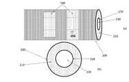
- FIGS. 2( a ) and ( b )show a capillary similar to that in FIG. 1 , both lengthwise (a) and in cross section (b) after the inner and outer surfaces have had conductive materials applied to form a hollow core coaxial cable. Shown in the figure are the conductive inner surface, 220 , the conductive outer surface, 200 , dielectric material, 210 , the hollow portion, approximately at the center, 230 . A selected portion of at least one of the outer conductive layer has been removed to form a pattern, 240 . Note that the pattern can be completely removed around the circumference of the capillary or only partially removed. In like manner, a portion of the conductive inner surface has been removed, 250 .
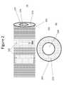
- FIG. 3shows, in cross section, a holey fiber or photonic crystal coaxial cable, having a central capillary, 330 , and a plurality of outer capillaries, 320 , surrounding the central capillary, wherein all capillaries run approximately parallel to the long axis.
- the holey fiber coaxial cableis made from a dielectric material, 340 .
- the inner surface of the central capillaryis coated with a conductor, 300
- the outer surface of the holey fiber coaxial cable, 310is also coated with a conductor.
- FIG. 4shows a cross section of a portion of a hollow core coaxial cable similar to that shown in FIG. 2 but with an additional polymer dielectric coating and optional conductor layer, wherein, optionally, selected portions of the conductive layers has been removed to form patterns.
- FIG. 4shows a capillary comprising a dielectric material, 400 , wherein the capillary is hollow approximately at the center, 405 .
- On the inside wall of the capillary, there is a conductive coating, 410which is optionally removed to form a pattern, 420 , optionally, leaving behind segmented portions of conductive coating, 415 .
- a conductive coating, 425which is optionally removed to form a pattern in the outer conductive coating, 435 , and smaller segmented portions of conductive coating, for example, 430 .
- the conductor coated capillaryis coated with a dielectric polymer coating, 460 , which, in turn, is optionally, coated with a conductor, 445 , wherein portions of the conductor are optionally removed to form a pattern in the conductive coating, 465 , and smaller segmented portions of conductive coating, 470 .
- FIG. 4shows an optional conducting via structure, 440 , which electrically connects the conductor, 445 , on the outer layer of the dielectric polymer coating, 460 , and the conductor, 425 , on the outside wall of the capillary. Also shown is an optional conducting via structure, 455 , which electrically connects the conductor, 425 , in the outside wall of the capillary with the conductor, 410 , on the inside wall of the capillary.
- the via structures, 440 and 455can be aligned or out of alignment as required.
- the patterns in the conductorscan be aligned or out of alignment as required.
- the conductor patternscan have the conductive material removed around the full circumference or on every face or they can be removed partially as required.
- the patterncan be thought of either positively or negatively, so that conductive materials can be deposited in the desired areas or removed from the desired areas.
- Such patterned and interconnected featuresenable coaxial or triaxial configurations with patterns and shorts that allow one skilled in the art to produce one or more of antennas, baluns, filters, etc.
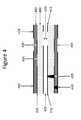
- FIG. 5( a )shows a connector, 500 , used, in this example, to connect two hollow core coaxial cables. Shown in the figure is the central ferrule, 505 , with a longitudinal passage, 510 . The capillary, 515 , is shown inserted into the longitudinal passage of the ferrule.
- FIG. 5( b )shows the body of the ferrule, 505 , in cross section, wherein the end face of the ferrule, 520 , is optionally capped by a metal ring, 525 , also shown in cross section. If the ferrule is a conductor, the metal ring may not be required.
- the hollow center of the hollow core coaxial cable, 535the dielectric material of the hollow core coaxial cable, 530 , the inner surface of the hollow core coaxial cable coated with a conductor, 540 , the outer surface of the hollow core coaxial cable coated with a conductor, 545 , configured such that the coated outer surface of the hollow core coaxial cable is in electrical contact with the metal ring, 525 , that caps the end of the ferrule.
- a metal insert, 550in the end of the hollow core coaxial cable. The metal insert is itself hollow. Further shown in FIG.
- FIG. 5( b )is a second assembly, 555 , that is similar to that in 505 - 550 but configured so as to be face-to-face with the first assembly.
- the conductor on the inner surface of the first capillaryis brought into electrical contact with the conductor on the inner surface of the second hollow core coaxial cable via their respective metal inserts.
- the conductor on the outer surface of the first hollow core coaxial cableis brought into electrical contact with the conductor on the outer surface of the first hollow core coaxial cable via contact with their respective metal rings on the ferrule end faces or by the ferrule end faces themselves if the ferrule is conductive.
- FIG. 5( c )shows a structure similar to FIG.
- the capillaryhaving a dielectric material, 530 , a hollow core, 535 , a conductor coated on its inside surface, 540 , and its outside surface, 545 , is shown cemented into the ferrule with cement, 560 .
- the capillaryis shown protruding from the end of the semispherical ferrule so that it can make contact with a mated ferrule. Also shown is a sealant for sealing the end of the capillary, 565 .
- FIG. 6( a )shows a ribbon cable made from a plurality of hollow core coaxial cables, 610 , surrounded by a sheath which may comprise optional buffer layer, 615 , further surrounded by a binder, 620 , still further surrounded by an optional strength member, 625 , and surrounded by a jacket, 630 .
- FIG. 6( b )shows a plurality of hollow core coaxial cables, each having an inner surface coated with a conductor, 635 .
- the capillaryis made of a dielectric, material, 640 , and has an outer surface coated with a conductor, 645 .
- each hollow core coaxial cablehas an inner surface coated with a conductor, 650 .
- the capillaryis made of a dielectric, material, 655 , and has an outer surface coated with a conductor, 660 .
- the hollow core coaxial cablesare each coated with a dielectric sheathing material, 665 , which insulates the respective conductors on the outer surfaces of the individual hollow core coaxial cables.
- the independent conductorscan provide independent DC power and/or lower frequency signals while the coax provides microwave signals or power transmission.
- the contiguous portions of the sheathing material on each hollow core coaxial cablecan be commingled with that from a neighboring cable to produce a free-standing ribbon or not commingled to produce a loose array.
- FIG. 7such hollow core coaxial cables can be packaged in a larger capillary or tube or jacket.
- FIG. 7( a )shows, in cross section, a bundle of hollow core coaxial cables with a sheath as in FIG. 6 , shown here as one layer, 700 , individual hollow core coaxial cables, 705 , and a central hollow core coaxial cable, 710 .
- Such a packagecan also be used to provide a cooling loop to remove heat generated when the cables are used to deliver power. In this case, as shown in FIG.
- FIG. 7( b )there is a sheath as above, 750 , individual hollow core coaxial cables, 755 , and a central conduit, 760 , that functions as an independent feed tube that provides part or the cooling loop, using fluids such as gases, condensed gases or other cooling liquids, which are returned through the interstitial voids between hollow core coaxial cables, 765 , or vice versa.
- the center of one or more coax cablescan also be used to delivery or receive one or more fluids.
- FIGS. 8( a ) and ( b )illustrate a further use for hollow core coaxial cables.
- a hollow core coaxial cable, 800having a hollow core, 805 , a conductor on the inner surface, 810 , a conductor on the outer surface, 815 , and a dielectric, 825 , between the conductors, interfaced to a module that acts as a sensor, transducer or actuator, 820 .
- a laseris used to provide power to the module, 820 , via the hollow core, 805 .
- the hollow coreacts as a waveguide to provide a low-loss power to the module. Shown in FIG.
- FIG. 8( b )is a hollow core coaxial cable, 850 , having a hollow core, 855 , a conductor on the inner surface, 860 , a conductor on the outer surface, 865 , and a dielectric, 875 , between the conductors, interfaced to a module that acts as a sensor, transducer or actuator, 870 .
- a laseris used to provide an optical signal to the module, 870 , via the hollow core, 855 .
- the hollow coreacts as a waveguide to provide a low-loss optical signal to the module, 870 .
- the optical signalis converted to an electrical signal and is returned through one or both of the hollow core coaxial cable conductors, 860 , 865 .
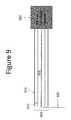
- FIG. 9shows a hollow core coaxial cable, 900 , having a hollow core, 905 , a conductor on the inner surface, 910 , and a conductor on the outer surface, 915 , interfaced to a module that acts a sensor, transducer or actuator, 920 .
- a conducting wire, 925is used to provide power or a signal to the module, 820 .
- the wire, 925may be insulated to prevent electrical contact with the conductor on the inner surface of the hollow core coaxial cable, 905 .
- FIG. 10shows how hollow core coaxial cables can function as switched antennas.
- FIG. 10shows a bundle of nine hollow core coaxial cables, 1000 , with eight of the cables arranged generally on the vertices of an octahedron and one hollow core coaxial cable in the center.
- Four of the hollow core coaxial cablesare selectively switched on, 1005
- five of the hollow core coaxial cables, including the one in the centerare selectively switched off, 1010 .
- the directional properties of an RF signalcan be selectively manipulated using the switched array.
- FIG. 10shows a plot of signal intensity as a function of the angle of azimuth, wherein a directional cardioid pattern is obtained, 1015 .
- dielectricrefers to a material property wherein the conductivity of the material is less than about 10 ⁇ 10 Siemens per meter.
- a coating “on” a specific layerwhen referring to a coating “on” a specific layer, it includes a coating directly onto the specified layer and may include one or more additional layers between the coating and the specified layer.
- holey fiberrefers to a fiber in which a plurality of holes, channels, capillaries and other voids are distributed evenly or unevenly throughout at least a portion of the fiber.
- viarefers to a channel connecting one or more layers
- hollow core coaxial cablescomprising a dielectric capillary having at least one inside wall and at least one outside wall, at least one inner conducive layer on the inner wall of the capillary, and at least one outer conductive layer disposed on the outer wall of the capillary.
- a hollow core high frequency coaxial cablecomprising: providing a hollow core dielectric hollow core coaxial cable having an inside wall and an outside wall and a conductor disposed on the inside wall of the hollow core coaxial cable; depositing a conductor on the outside wall of the hollow core coaxial cable.
- holey fiber coaxial cablescomprising: a holey fiber dielectric capillary having at least one inside wall and an outside wall; an inner conductive layer on the at least one inside wall of the hollow core coaxial cable; and an outer conductive layer on the outside wall of the holey fiber capillary.
- Holey fiber capillarieshave been developed for photonic applications. Where the number of holes is large compared to the wavelength, it is also known as holey fiber or photonic crystal waveguide.
- the dielectric constant, as well as the loss due to the dielectriccan be reduced by substantially reducing the effective quantity of dielectric in the cross-section of the coaxial cable. Further the dielectric can be anisotropically distributed in cross-section to produce effects such as polarization maintenance for the propagating waves.
- multiple cableshaving two or more hollow core coaxial cables forming a ribbon or bundled into a generally round cross section. Selected hollow core coaxial cables of the multiple cable may further be switched. Further disclosed and claimed are methods of non-symmetrically switching the hollow core coaxial cables of the multiple cable to allow creation of a directional antenna which allows for steering RF signal toward a preferred direction.
- the dielectric capillary or the holey fiber capillarycan have a capillary cross section chosen from circular, oval, elliptical, triangular, square, rectangular, or hexagonal.
- the cross-section of the inner capillary hole and the outside of the dielectriccan be of the same shape or different shapes.
- the insidemay be an oval or rectangular to preserve polarization if the inside diameter were used for sub millimeter or terahertz waveguiding.
- Both the inner conductor and outer conductormay be shaped anisotropically to preserve one or more polarization states for the coaxial cable.
- Such techniques of formation of custom capillariesare known in the art of drawing optical fibers and capillaries and typically involve first firming a larger scale glass structure, tube, rod or assembly of glass tubes, plates, and rods and to fuse these elements together to form a larger scale preform containing the desired cross-sectional elements.
- the preformis placed into a chuck in an elevated furnace where a portion of the preform melts and drops.
- a fiberremains attached between the preform and the molten drop and the glass capillary or fiber is then drawn on a capstan where the rate of pull and rate of feed into of the preform into the furnace are carefully controlled based on feedback from measurements such as outside diameter of the fiber or capillary, which is typically measured using a laser micrometer.
- Secondary polymer and metal coatingsare often applied to the fiber or capillary on the draw tower itself before spooling it.
- a selected portion of the inner conductive layercan be removed to form a pattern. Still further, a selected portion of the outer conductive layer can be removed to form a pattern.
- Vias through the dielectric of the coaxial cable of various shapesmay be made by such method as, for example, machining, etching or removing by laser ablation at selected locations for various reasons such as to allow electrical shorting, fluid flow or a mechanical connection.
- Such selective removal of the conductive layers and/or dielectricscan enable the integral formation of antennas, impedance transformers, baluns, or enable the integration of mounting regions for switch elements, diodes, or other electrical, mechanical, sensing, or transducing elements.
- Means for switching RF signalsinclude mechanical switches, electromechanical switches, optical switches including optical transistors, modular bidirectional switches, coaxial switches, diodes, pin diodes or monolithic microwave integrated circuits (MMIC) and applications specific integrated circuit (ASIC) based circuits, two-position switches, splitters, combiners, line couplers, switch arrays, stacked switch arrays, multiplexers, demultiplexers, electronically and optically switched pin diode arrays, equivalents of the above and combinations of the above.
- MMICmonolithic microwave integrated circuits
- ASICapplications specific integrated circuit
- the hollow core coaxial cablecan have a polymer coating on the outer conductive layer. Still further, the hollow core coaxial cable can have a conductive material disposed on the polymer coating. Still further, a selected portion of the conductive material disposed on the polymer coating can be removed to form a pattern.
- the dielectric capillarycan comprise one or more dielectric materials such as, for example, silica, fused quartz, fused silica, low —OH fused silica, glass, TeflonTM, fluoropolymer, borosilicate glass, polyethylene, polytetrafluoroethylene, fluorinated ethylene-propylene, perfluoroalkoxy polyolefin, porous fluoropolymer, polypropylene, nylon 6, nylon 11, silicone rubber, rubber, polyvinyl chloride, polystyrene or other dielectric materials that can be drawn, cast, molded, extruded, and/or otherwise formed.
- dielectric materialssuch as, for example, silica, fused quartz, fused silica, low —OH fused silica, glass, TeflonTM, fluoropolymer, borosilicate glass, polyethylene, polytetrafluoroethylene, fluorinated ethylene-propylene, perfluoroalkoxy polyole
- the inner conductive layercan comprise one or more metals chosen from silver, nickel, copper, gold, platinum, palladium, molybdenum, tungsten, tantalum or titanium.
- outer conductive layercan comprise one or more metals chosen from silver, nickel, copper, gold, platinum, palladium, molybdenum, tungsten, tantalum or titanium.
- the conductive material disposed on the polymer coatingcomprises one or more metals chosen from silver, nickel, copper, gold, platinum, palladium, molybdenum, tungsten, tantalum or titanium.
- Other metalsincluding alloys that are known in the art of deposition through chemical, electrochemical, or vapor deposition means may be chosen.
- a method of making a hollow core high frequency coaxial cablecomprising: providing a hollow core dielectric capillary having an inside wall and an outside wall and a conductor disposed on the inside wall of the capillary; and depositing a conductor on the outside wall of the capillary.
- the methodcan further comprise removing a selected portion of the conductor disposed on the inside wall of the capillary. Further, the method can further comprise removing a selected portion of the conductor on the outside wall of the capillary.
- Removing a selected portion of the conductor disposed on the inside wall of the hollow core coaxial cablecan be done by such methods as, for example, ablating the conductor disposed on the inside wall of the hollow core coaxial cable with a laser, such as, for example, a carbon dioxide laser, a KrF Excimer laser, an ArF Excimer laser, an F2 excimer laser, a frequency doubled neodymium YAG (yttrium aluminum garnet) laser or a frequency tripled Yb:KYW (ytterbium in a matrix of potassium yttrium tungstate) laser.
- a lasersuch as, for example, a carbon dioxide laser, a KrF Excimer laser, an ArF Excimer laser, an F2 excimer laser, a frequency doubled neodymium YAG (yttrium aluminum garnet) laser or a frequency tripled Yb:KYW (ytterbium in a matrix of potassium yttrium
- Removing a selected portion of the conductor on the outside wall of the hollow core coaxial cablecan be done by such methods as, for example, ablating a selected portion of the conductor on the outside wall of the hollow core coaxial cable with a laser, such as, for example, carbon dioxide laser, a KrF Excimer laser, an ArF Excimer laser, an F2 excimer laser, a frequency doubled neodymium YAG laser or a frequency tripled Yb:KYW laser.
- the methodcan further comprise: applying a photoresist to the conductor on the outside wall of the hollow core coaxial cable; image wise patterning the photoresist; and etching a selected portion of the conductor on the outside wall of the hollow core coaxial cable.
- depositing a conductor on the outside wall of the hollow core coaxial cableis done by one or more of electroless plating, electroplating, sputtering, chemical vapor deposition or atomic layer deposition.
- the methodcan further comprise applying a polymer coating to the conductor on the outside wall of the hollow core coaxial cable.
- the polymer coatingcan be applied by dip coating, spray coating chemical vapor coating or electrophoretic coating.
- the methodcan further comprise depositing a conductor on the polymer coating.
- the methodcan further comprise removing a selected portion of the conductor on the polymer coating.
- the dielectricmay be etched selectively or patterned using one or more of the methods outlined above such as by laser, patterning and etching, or by mechanical removal.
- Capillaries and holey finer capillariesare understood to have inside walls and outside walls.
- Hollow core coaxial cable wallscomprise materials that generally function as dielectrics in the desired frequency range.
- the cross sectional shape of the capillaries depicted in FIG. 1-4are generally round, it is understood that the cross sectional shape can be of any geometry such as square, rectangular or round, symmetrical or non symmetrical, to allow optimization for the application.
- the capillariesthemselves may be porous or may comprise many to thousands of hollow regions reducing the dielectric constant.
- Capillariescan have different inner and outer diameters and dimensions, depending on the desired frequency range. When dimensions other than diameters are specified, the measurement is made from flat face to flat face. Capillaries are coated with a polyimide or acrylic coating to give them strength. Coating thickness from about 10 ⁇ m (microns) to about 100 ⁇ m (microns) can be used.
- inner diameters or dimensionscan be from about 25 to about 700 ⁇ m (microns).
- inner diameters or dimensionscan be from about 75 to about 400 ⁇ m (microns).
- inner diameters or dimensionscan be from about 75 to about 200 ⁇ m (microns).
- outer diameters or dimensionscan be from about 100 to about 850 ⁇ m (microns). Within that range, outer diameters or dimensions can be from about 100 to about 650 ⁇ m (microns). Within that range, outer diameters or dimensions can be from about 100 to about 360 ⁇ m (microns).
- a hollow core holey fibercomprises a large center capillary surrounded by a plurality of smaller capillaries, also referred to as the holey cladding.
- the holey fibercan have an outer wall of fused silica or other dielectric material.
- the holey fibermay have a polymer coating of acrylic or polyimide.
- the outside polymer coatingmay have a thickness of from 10-100 ⁇ m (microns).
- the center capillarycan have, for example, a diameter of about 5 to about 150 ⁇ m (microns).
- the center capillarycan have a diameter 8 to about 100 ⁇ m (microns).
- the center capillarycan have a diameter from about 9 to about 75 ⁇ m (microns).
- the distance between centers of the smaller capillariescan be between about 1 to about 20 ⁇ m (microns).
- the distance between centers of the smaller capillariescan be between about 1.5 to about 15 ⁇ m (microns).
- the distance between centers of the smaller capillariescan be between about 2 to about 10 ⁇ m (microns).
- a plurality of smaller capillariessurrounds the larger center capillary, forming a holey cladding.
- One way to characterize the holey cladding in addition to the distance between centers measurement, supra,is the thickness of the holey cladding as measured from the outside of the large center capillary to the edge of the outer wall.
- the thickness of the holey claddingcan be from about 10 to about 200 ⁇ m (microns). As a further example, the thickness of the holey cladding can be from about 20 to about 100 ⁇ m (microns). As a still further example, the thickness of the holey cladding can be from about 25 to about 75 ⁇ m (microns).
- the thickness of the outer wallcan be, for example, from about 10 to about 200 ⁇ m (microns). As a further example, the thickness of the outer wall can be from about 15 to about 100 ⁇ m (microns). As a still further example, the thickness of the outer wall can be from about 20 to about 50 ⁇ m (microns).
- the conductor thicknesses on the inside wall of the center capillary and the outside of the outer wallcan be the same or different.
- conductor thicknesses on the inside wall of the center capillary and the outside of the outer wallcan be from about 0.05 to about 20 ⁇ m (microns).
- the conductor thicknesses on the inside wall of the center capillary and the outside of the outer wallcan be from about 0.5 to about 10 ⁇ m (microns).
- the conductor thicknesses on the inside wall of the center capillary and the outside of the outer wallcan be from about 0.75 to about 5 ⁇ m (microns).
- the selection of the metal thicknessmay depend on the type of metal and the frequency of the signal to be carried.
- More than one hollow coaxial cablemay be combined to form a ribbon structure or may be bundled in a generally round cross section which can allow for a plethora of singles to propagate at the same time.
- the hollow core coaxial cables of the multiple cablemay be individually switched in a non-symmetrical manner such that a radiation pattern may be generated. The pattern may be detected which would allow for the multiple cable to be directed when the cable is not visible, such as, for example, in the human body as the multiple cable may allow the precise positioning of a probe, a surgical device, an implant or the like.
- the radiating multiple cableis especially useful when optical methods are hampered such as, for example, when there is a lot of blood that would blind optical devices.
- wateris understood to be deionized water, unless otherwise stated, however, deionized water is not required.
- conductorsgenerally function as such in the frequency range of interest.
- the coaxial cables and waveguides, described herein,may or may not be flexible but do function in straight or bent configurations.
- temperatureis controlled by placing the outside of the hollow core coaxial cable in a water bath having the desired temperature. To heat at temperatures above about 80° C. the hollow core coaxial cable is placed in an oven.
- metal layersas the conductive material
- other materialsmay also be used, such as, for example graphene, carbon nanoparticles, organic conductive materials, such as, for example, polythiophene, polyacetylene, polypyrrole, polyaniline and the like, and other non-metallic conductive materials known in the art.
- Plating the interior walls of capillariescan be accomplished by electroless plating, or electroless plating followed by electroplating. These operations are usually accomplished by flowing solutions through the hollow core coaxial cable. In flowing solutions through capillaries, flow rates in ml/min are estimated according to Poiseuille's Equation for a hollow core coaxial cable of circular cross section:
- ris the radius in ⁇ m
- ⁇ Pis the pressure in lb/in 2
- ⁇is the viscosity in centipoise
- Lis in cm.
- the radiusis conveniently approximated by 1 ⁇ 2 the average flat-to-flat dimension.
- Plating of the interior and exterior walls of capillariescan further be accomplished by chemical vapor deposition (CVD) in which a hot precursor containing the desired metal atom is decomposed to the metal, thermally or in a plasma.
- CVDchemical vapor deposition
- a hot precursor containing the desired metal atomis decomposed to the metal, thermally or in a plasma.
- Mo, Ta and Tiare deposited by low pressure CVD, from their pentachlorides according to the reaction: 2 MCl 5 +5 H 2 ⁇ 2 M+10 HCl
- Tungstenis deposited from tungsten hexafluoride in one of two ways: WF 6 ⁇ W+3 F 2 WF 6 +3 H 2 ⁇ W+6 HF
- Nickel, molybdenum, and tungstenare deposited at temperatures above about 150° C. from their carbonyl precursors, Ni(CO) 4 , Mo(CO) 6 , W(CO) 6 .
- Carrier gassessuch as argon or nitrogen are used in various concentrations to control the deposition rate and morphology of the metal film.
- Goldis deposited from, for example, Trifluorophosphine Gold(I) Chloride, usually, using hydrogen as a carrier gas at temperatures above 110° C.
- another metalsuch as tantalum or platinum is deposited as a base.
- Palladiumis deposited from, for example, palladium(II) acetate at 200-300° C., using H 2 /He as a carrier gas.
- Platinumis deposited from, for example, trimethyl(ethylcyclopentadienyl)platinum (C 2 H 5 C 5 H 4 )Pt(CH 3 ) 3 , at temperatures above about 150° C., using argon as a carrier gas.
- signalscan enter or be transmitted out of the waveguide conductively by direct coupling or through one or more openings in the conductive coatings, optimized for the particular frequency in use.
- Pretreatment of fused quartz or silica inside and outside surfacescan be accomplished using a solution of sodium hypophosphite (about 100 gm/liter, buffered to pH 6-7 having a citrate or pyrophosphate buffer).
- Aqueous solutions of the organic boranesare also suitable such as dimethylamine borane, trimethylamine borane, diethylamine borane, triethylamine borane and pyridine borane.
- a suitable nonaqueous reductant solutionsuch as, for example di-isobutylaluminum hydride in hexane can also be used. Reducing gases may also be used such as hydrogen and carbon monoxide, optionally, with heating above about 100° C.
- a dilute solution of buffered hydrofluoric acid(20/1 to 40/1 dilution of the standard etching solution with dionized or distilled water).
- Polymer capillariesavailable from Paradigm Optics can also be used within the scope of this invention.
- Polymer materials usedcan be made of polyethylene, polyvinyl chloride, polytetrafluoroethylene, polycarbonates such as polyethylene teraphthalate, polyperfluoroalkoxy ethylene (PFA), and other fluorinated and non fluorinated polymers.
- Pretreatment of polymer based capillaries' inside and outside surfacescan be accomplished using a solution of sulphochromic acid at room temperature for a period of 20 minutes.
- Follow-on pretreatmentcan optionally be accomplished using a solution of sodium hypophosphite (about 100 gm/liter, buffered to pH 6-7 having a citrate or pyrophosphate buffer).
- Aqueous solutions of the organic boranesare also suitable such as dimethylamine borane, trimethylamine borane, diethylamine borane, triethylamine borane and pyridine borane.
- a suitable nonaqueous reductant solutionsuch as, for example, di-isobutylaluminum hydride in hexane can also be used.
- Reducing gasesmay also be used such as hydrogen and carbon monoxide, optionally, with heating above about 100° C.
- a solution of sodium hypophosphiteis prepared (about 100 g/dm 3 sodium hypophosphite in water, buffered to pH 6-7 using a pyrophosphate buffer).
- a solution of SnCl 2 /HCl in dionized water(SnCl 2 , 70 g/dm 3 , HCl (concentrated ⁇ 37%), 40 g/dm 3 ) is prepared.
- a solution of PdCl 2 /HCl in deionized water(PdCl 2 , 1 g/dm 3 , HCl (concentrated ⁇ 37%), 5 ml/dm 3 ) is prepared.
- the followingis used as a silver-Plating precursor: These materials are dissolved on order in a small amount of water: AgNO 3 (5 g), dodecylbenzene sulfonic acid sodium salt (30 mg), aqueous ammonia solution (concentrated ⁇ 28%, 25 ml). To the resulting solution, glacial acetic acid is added so that the final pH is reduced to 6-9. The volume of the solution is then increased to about 100 ml by adding deionized water so that the Ag + concentration is about 0.3 mole/dm 3 .
- a 3 mole/dm 3 aqueous stock solution of hydrazine hydrate(NH 2 HN 2 —H 2 O) is diluted with deionized water to give a concentration of about 0.3 moles/dm 3 solution.
- Solution D precursor25 ml
- Solution E reducer6 ml
- a 3 mole/dm 3 aqueous stock solution of an aldose sugar reducing agent such as glucoseis diluted with deionized water to give a concentration of about 0.3 moles/dm 3 solution.
- allose, altrose, mannose, gulose, idose, galactose, or talosecan also be used in place of glucose.
- lower molecular weight sugarssuch as glycolaldehyde, glyceraldehydes, erythrose, threose, ribose, arabinose, xylose, or lyxose can be used in the same molar proportion as well as formaldehyde in the same molar proportion.
- Solution D precursor25 ml
- Solution G alternative reducerusing glucose as the aldose sugar reducing agent, 6 ml
- Solution D precursor25 ml
- Solution G alternative reducerusing glucose as the aldose sugar reducing agent, 6 ml
- nickel electroless plating solutionsuitable for plating at a temperature of 30-60° C. for example, about 54° C. to give a thickness of 0.75 ⁇ m:
- One (1) part sodium fluoride, 80 parts sodium succinate, 100 parts nickel sulfate, and 169 parts sodium hypophosphiteare combined with 500 parts deionized water.
- the followingis used as a copper electroless plating solution suitable for plating at a temperature of 25-60° C. for example, about 54° C.: To 250 ml of water are added, with stirring, cupric sulfate (CuSO 4 -5H 2 O—7.5 g), triethanolamine (N(CH 2 CH 2 OH) 3 —5.0 g), sodium hydroxide (NaOH sufficient to give a pH of 13.5—about 20 g), sodium cyanide (NaCN—0.5 g), formaldehyde, 40% in water (H 2 CO—40.0 g), water to make 1 dm 3 .
- cupric sulfateCuSO 4 -5H 2 O—7.5 g
- triethanolamineN(CH 2 CH 2 OH) 3 —5.0 g
- sodium hydroxideNaOH sufficient to give a pH of 13.5—about 20 g
- sodium cyanideNaCN—0.5 g
- formaldehyde40% in water (H 2 CO—40.0 g), water to make 1
- the followingis used as a copper electroless plating solution suitable for plating at a temperature of 25-40° C. for example, about 32° C.: To 250 ml of water are added, with stirring, cupric sulfate (CuSO 4 -5H 2 O—1.0 g), potassium sodium tartrate (NaKC 4 H 4 O 6 —2.7 g), sodium hydroxide (NaOH sufficient to give a pH of 13.5—about 20 g), sodium cyanide (NaCN—0.05 g), formaldehyde, 40% in water (H 2 CO—35.0 g), water to make 1 dm 3 .
- cupric sulfateCuSO 4 -5H 2 O—1.0 g
- potassium sodium tartrateNaKC 4 H 4 O 6 —2.7 g
- sodium hydroxideNaOH sufficient to give a pH of 13.5—about 20 g
- sodium cyanideNaCN—0.05 g
- formaldehyde40% in water (H 2 CO—35.0 g), water to make 1 dm
- a fused silica hollow core coaxial cable of generally square cross sectionwith an inner dimension of about 100 ⁇ m (measured flat to flat), an outer dimension of about 300 ⁇ m (measured flat to flat), a length of 10 cm, and coated with a polyimide coating such that the outer dimension of the coating is about 383 ⁇ m, and wherein a portion of the polyimide coating is removed to reveal a bare segment of hollow core coaxial cable of length 0.5 cm, and wherein the bare segment of hollow core coaxial cable has coated segments on either lengthwise side, is provided by Polymicro Technologies, of Phoenix, Ariz.
- Solution Ais urged through the capillary from a reservoir using a peristaltic pump, adjusted so that the average pressure is about 150 lb/in 2 to achieve a flow rate of approximately 1.0 ml/min for a period of about 10 min. Times are from first emergence from the hollow core coaxial cable. In like manner, successive solutions are urged through the hollow core coaxial cable according to Table 1:
- plating solutionis Solution I at a temperature of 54° C. instead of solution F, to produce a hollow core coaxial cable with nickel plated on the inside wall.
- plating solutionis Solution J at a temperature of 54° C. instead of solution F, to produce a hollow core coaxial cable with copper plated on the inside wall.
- plating solutionis Solution K at a temperature of 32° C. instead of solution F, to produce a hollow core coaxial cable with copper plated on the inside wall.
- any one of examples 1-5having a portion of the protective polyimide coating removed from the exterior wall of the hollow core coaxial cable, as described supra, is chosen. Removal of a portion of the conductive coating on one or more of the interior walls is accomplished by laser ablation using a 248 nm pulsed excimer laser, such as the Lumonics PM800 laser (300 mJ, 1-30 W), although other lasers and wavelengths may also be used.
- a 248 nm pulsed excimer lasersuch as the Lumonics PM800 laser (300 mJ, 1-30 W)
- the flatness of the faces of the capillariesenables selective ablation of conductive material from one or more selected sides.
- any one of examples 1-10 having a polyimide coating on some portion of the exterior wall of the capillaryis chosen and the ends of the hollow core coaxial cable are sealed with an epoxy-based formulation, such as SmartGelTM, available from Nye optical Products of Fairhaven, Mass.
- the outer wall of the hollow core coaxial cableis treated repeatedly with concentrated sulfuric acid at 100-130° C. to remove the polyimide coating and rinsed with deionized water. After rinsing, the hollow core coaxial cable is placed in successive baths to plate the outer surface at times and temperatures according to Table 2:
- the metal clad hollow core coaxial cableis optionally coated with a protective polyimide, acrylic or electrodeposited photoresist coating or subjected to further processing.
- plating solutionis Solution I at a temperature of 54° C. instead of solution F, to produce a hollow core coaxial cable with nickel plated on the outside wall.
- plating solutionis Solution J at a temperature of 54° C. instead of solution F, to produce a hollow core coaxial cable with copper plated on the outside wall.
- plating solutionis Solution K at a temperature of 32° C. instead of solution F, to produce a hollow core coaxial cable with copper plated on the outside wall.
- the hollow core coaxial cable of any one of examples 11-50is chosen. Removal of the metal coating from a portion of one or more of the exterior walls is accomplished by laser ablation using a 248 nm pulsed excimer laser, such as the Lumonics PM800 laser (300 mJ, 1-30 W), although other lasers and wavelengths may also be used.
- a 248 nm pulsed excimer lasersuch as the Lumonics PM800 laser (300 mJ, 1-30 W)
- the flatness of the faces of the capillariesenables selective image wise ablation of metal from one or more sides.
- the open area created by ablationcan be aligned with the ablated portions of the interior wall so that the open areas overlap or are masked respectively, as required for the particular use contemplated.
- a polymer coatingcan be disposed on the outside of the hollow core coaxial cable such as a polyimide or an acrylic or an electrodeposited resist, a suitable example of which is EAGLETM 2100 ED Negative acting electrodeposited photoresist, along with its ancillary developer, EAGLETM 2005 developer, available from the Dow Chemical Company.
- the resistis applied by direct current cataphoretical electro-deposition at a direct current potential of 70 Volts, bath temperature 45° C., baked at 100° C. for 20 minutes and may be bulk or image-wise photo-cured at a wavelength of 365 nm and a dose of 300-800 mJ/cm 2 , depending on the thickness of the coating.
- the polyimide coated hollow core coaxial cableis circular in cross section with a length of 20 cm, an inner diameter of about 150 ⁇ m, and the pressure is about 95 lb/in 2 , and adjusted to give a flow rate of about 1.5 ml/min, available from Polymicro Technologies, of Phoenix, Ariz.
- this hollow core coaxial cablehas a portion of its polyimide coating removed such that a bare segment of hollow core coaxial cable is visible with coated segments on either lengthwise side.
- any one of examples 91-95having a portion of the protective polyimide coating removed from the exterior wall of the hollow core coaxial cable, as described supra, is chosen.
- Image wise removal of a portion of the metal coating the interior wall of the hollow core coaxial cableis accomplished by laser ablation using a 248 nm pulsed excimer laser, such as the Lumonics PM800 laser (300 mJ, 1-30 W), although other lasers and wavelengths may also be used.
- plating solutionis Solution I at a temperature of 54° C. instead of solution F, to produce a hollow core coaxial cable with nickel plated on the outside wall.
- plating solutionis Solution J at a temperature of 54° C. instead of solution F, to produce a hollow core coaxial cable with copper plated on the outside wall.
- plating solutionis Solution K at a temperature of 32° C. instead of solution F, to produce a hollow core coaxial cable with copper plated on the outside wall.
- the hollow core coaxial cable of any one of examples 101-140is chosen. Image-wise removal of the metal coating from a portion of the exterior walls is accomplished by laser ablation using a 248 nm pulsed excimer laser, such as the Lumonics PM800 laser (300 mJ, 1-30 W), although other lasers and wavelengths may also be used.
- a 248 nm pulsed excimer lasersuch as the Lumonics PM800 laser (300 mJ, 1-30 W)
- the circular cross section geometry of the hollow core coaxial cabledoes not enable selective image wise laser ablation from individual faces.
- the open area created by ablationcan be aligned with the ablated portions of the interior wall so that the open areas overlap or are masked respectively, as required for the particular use contemplated.
- a polymer coatingcan be disposed on the outside of the hollow core coaxial cable such as a polyimide or an acrylic or an electrodeposited resist, a suitable example of which is EAGLETM 2100 ED Negative acting electrodeposited photoresist, along with its ancillary developer, EAGLETM 2005 developer, available from the Dow Chemical Company.
- the resistis applied by direct current cataphoretical electro-deposition at a direct current potential of 70 Volts, bath temperature 45° C., baked at 100° C. for 20 minutes and may be bulk or image-wise photo-cured at a wavelength of 365 nm and a dose of 300-800 mJ/cm 2 , depending on the thickness of the coating.
- any one of the polymer coated capillaries described in Examples 51-90 or 141-180can be used.
- the surfaces of the polymer coatingsare treated using a dilute solution of sulphochromic acid at room temperature for a period of 20 minutes. Pretreatment is continued using a solution of sodium hypophosphite (about 100 gm/liter, buffered to pH 6-7 with a pyrophosphate buffer). After rinsing thoroughly with deionized water, the polymer coated hollow core coaxial cable is placed in successive baths to plate the outer surface at times and temperatures according to Table 2. This produces a hollow core coaxial cable with three layers of metal.
- the hollow core coaxial cable with three layers of metal of example 181is subject to image wise laser ablation as described in Examples 141-180 so that a portion of the metal coating is ablated.
- a glass hollow core coaxial cable of 300 ⁇ m inner diameter and 400 ⁇ m outer diameter and a silver coating on the inside surface of about 10 ⁇ m of thickness and an acrylic coating on the outside surface of 175 ⁇ m of thickness (total outer diameter of about 750 ⁇ m)is provided by Polymicro Technologies, of Phoenix, Ariz.
- the acrylic coatingis removed with a gentle stream of acetone and the ends of the hollow core coaxial cable sealed with epoxy.
- the outer surface of the glass of the glass hollow core coaxial cableis treated using a solution of sodium hypophosphite (about 100 gm/liter, buffered to pH 6-7 with a pyrophosphate buffer) and rinsed thoroughly with water.
- the outer surface of the hollow core coaxial cableis treated sequentially with the solutions as in Table 2.
- a polymer coatingis disposed on the coaxial cable thus formed as described in, for example, Examples 141-180.
- the outer polymer coatingcan be coated once again with metal as described supra in Example 181.
- a glass hollow core coaxial cable of 300 ⁇ m inner diameter and 400 ⁇ m outer diameter and a silver coating on the inside surface of about 10 ⁇ m of thickness and an acrylic coating on the outside surface of 175 ⁇ m of thickness (total outer diameter of about 750 ⁇ m)is provided by Polymicro Technologies, of Phoenix, Ariz. A portion of the acrylic coating is removed with a gentle stream of acetone. The silver plated on the inner surface is then ablated image-wise as described supra in Examples 96-100. The ends of the hollow core coaxial cable sealed with epoxy.
- the outer surface of the glass of the glass hollow core coaxial cableis treated using a solution of sodium hypophosphite (about 100 gm/liter, buffered to pH 6-7 with a pyrophosphate buffer) and rinsed thoroughly with water. Thereafter, the outer surface of the hollow core coaxial cable is treated sequentially with the solutions as in Table 2.
- a portion of the silver on the outer surfaceis ablated image-wise as described in Examples 141-180.
- a polymer coatingis disposed on the coaxial cable thus formed as described in, for example, Examples 141-180.
- the outer polymer coatingcan be coated once again with metal as described supra in Example 181 and portions of the metal removed image-wise from the outer surface of the polymer coating.
- the hollow core coaxial cableis laid out in a vessel so that both open ends are covered when subjected to the desired solution at the desired temperature.
- the solutionis poured into the vessel and the vessel placed into a vacuum chamber.
- a vacuum of about 15 mm of mercury or lessis applied so that the fluid infuses the inside of the hollow core coaxial cable.
- the vesselis removed from the vacuum chamber, and allowed to stand for the prescribed amount of time.
- the hollow core coaxial cableis turned on end and placed on an absorbent mat so that the infused solution is drawn out.
- the hollow core coaxial cableis rinsed with dionized water several times in the vacuum chamber as above and subjected to treatment with the next solution or dried, as required. In this way, it is possible to simultaneously plate the insides and outsides of one or more capillaries.
- a holey fiber capillary coaxial cableis fabricated in the following way.
- a fused optical grade holey fiber with individual capillaries of about 100 ⁇ m and with lapped or cleaved endsis obtained from Newport Corporation of Irving, Calif. or NKT Photonics of Denmark.
- a plurality of individual capillaries in the holey fiberis obscured using an epoxy-based formulation such as SmartGelTM, available from Nye optical Products of Fairhaven, Mass.
- the holey fiberis placed in a high pressure jig, fitted with an o-ring assembly such that the obscured portions of the holey fiber face are on the upstream side of the jig.
- Solution Ais urged through the remaining channels of the holey fiber from a reservoir using a peristaltic pump, adjusted so that the average pressure is about 150 lb/in 2 to achieve a flow rate of approximately 1.0 ml/min for a period of about 10 min.
- Timesare from first emergence from the hollow core coaxial cable.
- successive solutionsare urged through the hollow core coaxial cable according to Table 1.
- the selected inner walls of the holey fiber,are coated with conductor and dried, the ends are fully sealed with SmartGelTM as above. After the SmartGelTM is cured, the hollow core coaxial cable is placed in successive baths to plate the outer surface at times and temperatures according to Table 2. The obscured ends of the holey fiber are then cut using a precision blade.
- the holey fiber coaxial cableis ready for use or further processing.
Landscapes
- Physics & Mathematics (AREA)
- Engineering & Computer Science (AREA)
- Manufacturing & Machinery (AREA)
- General Physics & Mathematics (AREA)
- Optics & Photonics (AREA)
- Communication Cables (AREA)
Abstract
Description
Where r is the radius in μm, ΔP is the pressure in lb/in2, η is the viscosity in centipoise and the length, L is in cm. For cross sections of other geometry, such as square, the radius is conveniently approximated by ½ the average flat-to-flat dimension.
2 MCl5+5 H2→2 M+10 HCl
WF6→W+3 F2
WF6+3 H2→W+6 HF
| TABLE 1 | |||
| Solution | Flow Rate, ml/min | Time, min | Temperature, ° C. |
| Water rinse | 1.0 | 10-20 | 25 |
| Solution B | 1.0 | 5 | 25 |
| Water rinse | 1.0 | 10-20 | 25 |
| Solution C | 1.0 | 3 | 25 |
| Water rinse | 1.0 | 10-20 | 25 |
| Solution F | 1.0 | 5 | 15-30 |
| Water rinse | 1.0 | 10-20 | 25 |
| TABLE 2 | ||||
| Solution | Time, min | Temperature, ° C. | ||
| Solution B | 5 | 25 | ||
| Water rinse | 10-20 | 25 | ||
| Solution C | 3 | 25 | ||
| Water rinse | 10-20 | 25 | ||
| Solution F | 5 | 15-30 | ||
| Water rinse | 10-20 | 25 | ||
After plating, the metal clad hollow core coaxial cable is optionally coated with a protective polyimide, acrylic or electrodeposited photoresist coating or subjected to further processing.
| TABLE 3 | |||
| Inside Wall, | Outside Wall | ||
| Frequency, gHz | Dia., μm | Dia., μm | Dielectric Loss, dB |
| 0.915 | 100 | 500 | ~0.7 |
| 0.915 | 200 | 1000 | ~0.4 |
| 2.45 | 100 | 500 | ~1.05 |
| 2.45 | 300 | 1000 | ~0.6 |
Claims (30)
Priority Applications (2)
| Application Number | Priority Date | Filing Date | Title |
|---|---|---|---|
| US13/183,409US9088074B2 (en) | 2011-07-14 | 2011-07-14 | Hollow core coaxial cables and methods of making the same |
| US14/804,203US9570787B2 (en) | 2011-07-14 | 2015-07-20 | Hollow core coaxial cables and methods of making the same |
Applications Claiming Priority (1)
| Application Number | Priority Date | Filing Date | Title |
|---|---|---|---|
| US13/183,409US9088074B2 (en) | 2011-07-14 | 2011-07-14 | Hollow core coaxial cables and methods of making the same |
Related Child Applications (1)
| Application Number | Title | Priority Date | Filing Date |
|---|---|---|---|
| US14/804,203ContinuationUS9570787B2 (en) | 2011-07-14 | 2015-07-20 | Hollow core coaxial cables and methods of making the same |
Publications (2)
| Publication Number | Publication Date |
|---|---|
| US20130016022A1 US20130016022A1 (en) | 2013-01-17 |
| US9088074B2true US9088074B2 (en) | 2015-07-21 |
Family
ID=47518641
Family Applications (2)
| Application Number | Title | Priority Date | Filing Date |
|---|---|---|---|
| US13/183,409Expired - Fee RelatedUS9088074B2 (en) | 2011-07-14 | 2011-07-14 | Hollow core coaxial cables and methods of making the same |
| US14/804,203Expired - Fee RelatedUS9570787B2 (en) | 2011-07-14 | 2015-07-20 | Hollow core coaxial cables and methods of making the same |
Family Applications After (1)
| Application Number | Title | Priority Date | Filing Date |
|---|---|---|---|
| US14/804,203Expired - Fee RelatedUS9570787B2 (en) | 2011-07-14 | 2015-07-20 | Hollow core coaxial cables and methods of making the same |
Country Status (1)
| Country | Link |
|---|---|
| US (2) | US9088074B2 (en) |
Cited By (4)
| Publication number | Priority date | Publication date | Assignee | Title |
|---|---|---|---|---|
| US20160072238A1 (en)* | 2014-09-09 | 2016-03-10 | Panasonic Avionics Corporation | Cable, method of manufacture, and cable assembly |
| US11011286B2 (en)* | 2018-12-10 | 2021-05-18 | Hitachi Metals, Ltd. | Cable |
| US11333825B2 (en) | 2019-11-07 | 2022-05-17 | Asml Netherlands B.V. | Method of manufacture of a capillary for a hollow-core photonic crystal fiber |
| US20220236509A1 (en)* | 2021-01-22 | 2022-07-28 | Macleon, LLC | Optical fiber cable |
Families Citing this family (192)
| Publication number | Priority date | Publication date | Assignee | Title |
|---|---|---|---|---|
| US10009065B2 (en) | 2012-12-05 | 2018-06-26 | At&T Intellectual Property I, L.P. | Backhaul link for distributed antenna system |
| US9113347B2 (en) | 2012-12-05 | 2015-08-18 | At&T Intellectual Property I, Lp | Backhaul link for distributed antenna system |
| US9300029B2 (en)* | 2013-03-15 | 2016-03-29 | International Business Machines Corporation | Coaxial transmission line slot filter with absorptive matrix |
| US9515366B2 (en)* | 2013-03-19 | 2016-12-06 | Texas Instruments Incorporated | Printed circuit board dielectric waveguide core and metallic waveguide end |
| US9999038B2 (en) | 2013-05-31 | 2018-06-12 | At&T Intellectual Property I, L.P. | Remote distributed antenna system |
| US9525524B2 (en) | 2013-05-31 | 2016-12-20 | At&T Intellectual Property I, L.P. | Remote distributed antenna system |
| US11034607B2 (en)* | 2013-09-20 | 2021-06-15 | University Of Southampton | Hollow-core photonic bandgap fibers and methods of manufacturing the same |
| JP6075639B2 (en)* | 2013-10-01 | 2017-02-08 | タツタ電線株式会社 | coaxial cable |
| US8897697B1 (en) | 2013-11-06 | 2014-11-25 | At&T Intellectual Property I, Lp | Millimeter-wave surface-wave communications |
| US9209902B2 (en) | 2013-12-10 | 2015-12-08 | At&T Intellectual Property I, L.P. | Quasi-optical coupler |
| US9692101B2 (en) | 2014-08-26 | 2017-06-27 | At&T Intellectual Property I, L.P. | Guided wave couplers for coupling electromagnetic waves between a waveguide surface and a surface of a wire |
| US9768833B2 (en) | 2014-09-15 | 2017-09-19 | At&T Intellectual Property I, L.P. | Method and apparatus for sensing a condition in a transmission medium of electromagnetic waves |
| US10063280B2 (en) | 2014-09-17 | 2018-08-28 | At&T Intellectual Property I, L.P. | Monitoring and mitigating conditions in a communication network |
| US9628854B2 (en) | 2014-09-29 | 2017-04-18 | At&T Intellectual Property I, L.P. | Method and apparatus for distributing content in a communication network |
| US9615269B2 (en) | 2014-10-02 | 2017-04-04 | At&T Intellectual Property I, L.P. | Method and apparatus that provides fault tolerance in a communication network |
| US9685992B2 (en) | 2014-10-03 | 2017-06-20 | At&T Intellectual Property I, L.P. | Circuit panel network and methods thereof |
| US9503189B2 (en) | 2014-10-10 | 2016-11-22 | At&T Intellectual Property I, L.P. | Method and apparatus for arranging communication sessions in a communication system |
| US9762289B2 (en) | 2014-10-14 | 2017-09-12 | At&T Intellectual Property I, L.P. | Method and apparatus for transmitting or receiving signals in a transportation system |
| US9973299B2 (en) | 2014-10-14 | 2018-05-15 | At&T Intellectual Property I, L.P. | Method and apparatus for adjusting a mode of communication in a communication network |
| US9627768B2 (en) | 2014-10-21 | 2017-04-18 | At&T Intellectual Property I, L.P. | Guided-wave transmission device with non-fundamental mode propagation and methods for use therewith |
| US9653770B2 (en) | 2014-10-21 | 2017-05-16 | At&T Intellectual Property I, L.P. | Guided wave coupler, coupling module and methods for use therewith |
| US9312919B1 (en) | 2014-10-21 | 2016-04-12 | At&T Intellectual Property I, Lp | Transmission device with impairment compensation and methods for use therewith |
| US9577306B2 (en) | 2014-10-21 | 2017-02-21 | At&T Intellectual Property I, L.P. | Guided-wave transmission device and methods for use therewith |
| US9564947B2 (en) | 2014-10-21 | 2017-02-07 | At&T Intellectual Property I, L.P. | Guided-wave transmission device with diversity and methods for use therewith |
| US9780834B2 (en) | 2014-10-21 | 2017-10-03 | At&T Intellectual Property I, L.P. | Method and apparatus for transmitting electromagnetic waves |
| US9520945B2 (en) | 2014-10-21 | 2016-12-13 | At&T Intellectual Property I, L.P. | Apparatus for providing communication services and methods thereof |
| US9769020B2 (en) | 2014-10-21 | 2017-09-19 | At&T Intellectual Property I, L.P. | Method and apparatus for responding to events affecting communications in a communication network |
| US10505250B2 (en) | 2014-11-20 | 2019-12-10 | At&T Intellectual Property I, L.P. | Communication system having a cable with a plurality of stranded uninsulated conductors forming interstitial areas for propagating guided wave modes therein and methods of use |
| US9997819B2 (en) | 2015-06-09 | 2018-06-12 | At&T Intellectual Property I, L.P. | Transmission medium and method for facilitating propagation of electromagnetic waves via a core |
| US9544006B2 (en) | 2014-11-20 | 2017-01-10 | At&T Intellectual Property I, L.P. | Transmission device with mode division multiplexing and methods for use therewith |
| US10554454B2 (en) | 2014-11-20 | 2020-02-04 | At&T Intellectual Property I, L.P. | Methods and apparatus for inducing electromagnetic waves in a cable |
| US9680670B2 (en) | 2014-11-20 | 2017-06-13 | At&T Intellectual Property I, L.P. | Transmission device with channel equalization and control and methods for use therewith |
| US10411920B2 (en) | 2014-11-20 | 2019-09-10 | At&T Intellectual Property I, L.P. | Methods and apparatus for inducing electromagnetic waves within pathways of a cable |
| US10505252B2 (en) | 2014-11-20 | 2019-12-10 | At&T Intellectual Property I, L.P. | Communication system having a coupler for guiding electromagnetic waves through interstitial areas formed by a plurality of stranded uninsulated conductors and method of use |
| US10516555B2 (en) | 2014-11-20 | 2019-12-24 | At&T Intellectual Property I, L.P. | Methods and apparatus for creating interstitial areas in a cable |
| US10505248B2 (en) | 2014-11-20 | 2019-12-10 | At&T Intellectual Property I, L.P. | Communication cable having a plurality of uninsulated conductors forming interstitial areas for propagating electromagnetic waves therein and method of use |
| US10009067B2 (en) | 2014-12-04 | 2018-06-26 | At&T Intellectual Property I, L.P. | Method and apparatus for configuring a communication interface |
| US10505249B2 (en) | 2014-11-20 | 2019-12-10 | At&T Intellectual Property I, L.P. | Communication system having a cable with a plurality of stranded uninsulated conductors forming interstitial areas for guiding electromagnetic waves therein and method of use |
| US9800327B2 (en) | 2014-11-20 | 2017-10-24 | At&T Intellectual Property I, L.P. | Apparatus for controlling operations of a communication device and methods thereof |
| US9742462B2 (en) | 2014-12-04 | 2017-08-22 | At&T Intellectual Property I, L.P. | Transmission medium and communication interfaces and methods for use therewith |
| US9654173B2 (en) | 2014-11-20 | 2017-05-16 | At&T Intellectual Property I, L.P. | Apparatus for powering a communication device and methods thereof |
| US11025460B2 (en) | 2014-11-20 | 2021-06-01 | At&T Intellectual Property I, L.P. | Methods and apparatus for accessing interstitial areas of a cable |
| US9461706B1 (en) | 2015-07-31 | 2016-10-04 | At&T Intellectual Property I, Lp | Method and apparatus for exchanging communication signals |
| US9954287B2 (en) | 2014-11-20 | 2018-04-24 | At&T Intellectual Property I, L.P. | Apparatus for converting wireless signals and electromagnetic waves and methods thereof |
| US10340573B2 (en) | 2016-10-26 | 2019-07-02 | At&T Intellectual Property I, L.P. | Launcher with cylindrical coupling device and methods for use therewith |
| US10243784B2 (en) | 2014-11-20 | 2019-03-26 | At&T Intellectual Property I, L.P. | System for generating topology information and methods thereof |
| US10144036B2 (en) | 2015-01-30 | 2018-12-04 | At&T Intellectual Property I, L.P. | Method and apparatus for mitigating interference affecting a propagation of electromagnetic waves guided by a transmission medium |
| US9876570B2 (en) | 2015-02-20 | 2018-01-23 | At&T Intellectual Property I, Lp | Guided-wave transmission device with non-fundamental mode propagation and methods for use therewith |
| US9749013B2 (en) | 2015-03-17 | 2017-08-29 | At&T Intellectual Property I, L.P. | Method and apparatus for reducing attenuation of electromagnetic waves guided by a transmission medium |
| US9705561B2 (en) | 2015-04-24 | 2017-07-11 | At&T Intellectual Property I, L.P. | Directional coupling device and methods for use therewith |
| US10224981B2 (en) | 2015-04-24 | 2019-03-05 | At&T Intellectual Property I, Lp | Passive electrical coupling device and methods for use therewith |
| US9793954B2 (en) | 2015-04-28 | 2017-10-17 | At&T Intellectual Property I, L.P. | Magnetic coupling device and methods for use therewith |
| US9948354B2 (en) | 2015-04-28 | 2018-04-17 | At&T Intellectual Property I, L.P. | Magnetic coupling device with reflective plate and methods for use therewith |
| US9748626B2 (en) | 2015-05-14 | 2017-08-29 | At&T Intellectual Property I, L.P. | Plurality of cables having different cross-sectional shapes which are bundled together to form a transmission medium |
| US9490869B1 (en) | 2015-05-14 | 2016-11-08 | At&T Intellectual Property I, L.P. | Transmission medium having multiple cores and methods for use therewith |
| US9871282B2 (en) | 2015-05-14 | 2018-01-16 | At&T Intellectual Property I, L.P. | At least one transmission medium having a dielectric surface that is covered at least in part by a second dielectric |
| US10650940B2 (en) | 2015-05-15 | 2020-05-12 | At&T Intellectual Property I, L.P. | Transmission medium having a conductive material and methods for use therewith |
| US10679767B2 (en) | 2015-05-15 | 2020-06-09 | At&T Intellectual Property I, L.P. | Transmission medium having a conductive material and methods for use therewith |
| US9917341B2 (en) | 2015-05-27 | 2018-03-13 | At&T Intellectual Property I, L.P. | Apparatus and method for launching electromagnetic waves and for modifying radial dimensions of the propagating electromagnetic waves |
| US9866309B2 (en) | 2015-06-03 | 2018-01-09 | At&T Intellectual Property I, Lp | Host node device and methods for use therewith |
| US10348391B2 (en) | 2015-06-03 | 2019-07-09 | At&T Intellectual Property I, L.P. | Client node device with frequency conversion and methods for use therewith |
| US10103801B2 (en) | 2015-06-03 | 2018-10-16 | At&T Intellectual Property I, L.P. | Host node device and methods for use therewith |
| US10812174B2 (en) | 2015-06-03 | 2020-10-20 | At&T Intellectual Property I, L.P. | Client node device and methods for use therewith |
| US10154493B2 (en) | 2015-06-03 | 2018-12-11 | At&T Intellectual Property I, L.P. | Network termination and methods for use therewith |
| US9912381B2 (en) | 2015-06-03 | 2018-03-06 | At&T Intellectual Property I, Lp | Network termination and methods for use therewith |
| US9913139B2 (en) | 2015-06-09 | 2018-03-06 | At&T Intellectual Property I, L.P. | Signal fingerprinting for authentication of communicating devices |
| US9608692B2 (en) | 2015-06-11 | 2017-03-28 | At&T Intellectual Property I, L.P. | Repeater and methods for use therewith |
| US10142086B2 (en) | 2015-06-11 | 2018-11-27 | At&T Intellectual Property I, L.P. | Repeater and methods for use therewith |
| US9820146B2 (en) | 2015-06-12 | 2017-11-14 | At&T Intellectual Property I, L.P. | Method and apparatus for authentication and identity management of communicating devices |
| US9667317B2 (en) | 2015-06-15 | 2017-05-30 | At&T Intellectual Property I, L.P. | Method and apparatus for providing security using network traffic adjustments |
| US9509415B1 (en) | 2015-06-25 | 2016-11-29 | At&T Intellectual Property I, L.P. | Methods and apparatus for inducing a fundamental wave mode on a transmission medium |
| US9640850B2 (en) | 2015-06-25 | 2017-05-02 | At&T Intellectual Property I, L.P. | Methods and apparatus for inducing a non-fundamental wave mode on a transmission medium |
| US9865911B2 (en) | 2015-06-25 | 2018-01-09 | At&T Intellectual Property I, L.P. | Waveguide system for slot radiating first electromagnetic waves that are combined into a non-fundamental wave mode second electromagnetic wave on a transmission medium |
| US10044409B2 (en) | 2015-07-14 | 2018-08-07 | At&T Intellectual Property I, L.P. | Transmission medium and methods for use therewith |
| US10033107B2 (en) | 2015-07-14 | 2018-07-24 | At&T Intellectual Property I, L.P. | Method and apparatus for coupling an antenna to a device |
| US9722318B2 (en) | 2015-07-14 | 2017-08-01 | At&T Intellectual Property I, L.P. | Method and apparatus for coupling an antenna to a device |
| US9836957B2 (en) | 2015-07-14 | 2017-12-05 | At&T Intellectual Property I, L.P. | Method and apparatus for communicating with premises equipment |
| US10170840B2 (en) | 2015-07-14 | 2019-01-01 | At&T Intellectual Property I, L.P. | Apparatus and methods for sending or receiving electromagnetic signals |
| US9853342B2 (en) | 2015-07-14 | 2017-12-26 | At&T Intellectual Property I, L.P. | Dielectric transmission medium connector and methods for use therewith |
| US9847566B2 (en) | 2015-07-14 | 2017-12-19 | At&T Intellectual Property I, L.P. | Method and apparatus for adjusting a field of a signal to mitigate interference |
| US9882257B2 (en) | 2015-07-14 | 2018-01-30 | At&T Intellectual Property I, L.P. | Method and apparatus for launching a wave mode that mitigates interference |
| US10148016B2 (en) | 2015-07-14 | 2018-12-04 | At&T Intellectual Property I, L.P. | Apparatus and methods for communicating utilizing an antenna array |
| US10341142B2 (en) | 2015-07-14 | 2019-07-02 | At&T Intellectual Property I, L.P. | Apparatus and methods for generating non-interfering electromagnetic waves on an uninsulated conductor |
| US10320586B2 (en) | 2015-07-14 | 2019-06-11 | At&T Intellectual Property I, L.P. | Apparatus and methods for generating non-interfering electromagnetic waves on an insulated transmission medium |
| US10033108B2 (en) | 2015-07-14 | 2018-07-24 | At&T Intellectual Property I, L.P. | Apparatus and methods for generating an electromagnetic wave having a wave mode that mitigates interference |
| US9628116B2 (en) | 2015-07-14 | 2017-04-18 | At&T Intellectual Property I, L.P. | Apparatus and methods for transmitting wireless signals |
| US10205655B2 (en) | 2015-07-14 | 2019-02-12 | At&T Intellectual Property I, L.P. | Apparatus and methods for communicating utilizing an antenna array and multiple communication paths |
| US9793951B2 (en) | 2015-07-15 | 2017-10-17 | At&T Intellectual Property I, L.P. | Method and apparatus for launching a wave mode that mitigates interference |
| US10090606B2 (en) | 2015-07-15 | 2018-10-02 | At&T Intellectual Property I, L.P. | Antenna system with dielectric array and methods for use therewith |
| US9608740B2 (en) | 2015-07-15 | 2017-03-28 | At&T Intellectual Property I, L.P. | Method and apparatus for launching a wave mode that mitigates interference |
| US9948333B2 (en) | 2015-07-23 | 2018-04-17 | At&T Intellectual Property I, L.P. | Method and apparatus for wireless communications to mitigate interference |
| US9749053B2 (en) | 2015-07-23 | 2017-08-29 | At&T Intellectual Property I, L.P. | Node device, repeater and methods for use therewith |
| US9912027B2 (en) | 2015-07-23 | 2018-03-06 | At&T Intellectual Property I, L.P. | Method and apparatus for exchanging communication signals |
| US10784670B2 (en) | 2015-07-23 | 2020-09-22 | At&T Intellectual Property I, L.P. | Antenna support for aligning an antenna |
| US9871283B2 (en) | 2015-07-23 | 2018-01-16 | At&T Intellectual Property I, Lp | Transmission medium having a dielectric core comprised of plural members connected by a ball and socket configuration |
| US9735833B2 (en) | 2015-07-31 | 2017-08-15 | At&T Intellectual Property I, L.P. | Method and apparatus for communications management in a neighborhood network |
| US9967173B2 (en) | 2015-07-31 | 2018-05-08 | At&T Intellectual Property I, L.P. | Method and apparatus for authentication and identity management of communicating devices |
| US10020587B2 (en) | 2015-07-31 | 2018-07-10 | At&T Intellectual Property I, L.P. | Radial antenna and methods for use therewith |
| US9904535B2 (en) | 2015-09-14 | 2018-02-27 | At&T Intellectual Property I, L.P. | Method and apparatus for distributing software |
| US10051629B2 (en) | 2015-09-16 | 2018-08-14 | At&T Intellectual Property I, L.P. | Method and apparatus for use with a radio distributed antenna system having an in-band reference signal |
| US10079661B2 (en) | 2015-09-16 | 2018-09-18 | At&T Intellectual Property I, L.P. | Method and apparatus for use with a radio distributed antenna system having a clock reference |
| US10009901B2 (en) | 2015-09-16 | 2018-06-26 | At&T Intellectual Property I, L.P. | Method, apparatus, and computer-readable storage medium for managing utilization of wireless resources between base stations |
| US10136434B2 (en) | 2015-09-16 | 2018-11-20 | At&T Intellectual Property I, L.P. | Method and apparatus for use with a radio distributed antenna system having an ultra-wideband control channel |
| US10009063B2 (en) | 2015-09-16 | 2018-06-26 | At&T Intellectual Property I, L.P. | Method and apparatus for use with a radio distributed antenna system having an out-of-band reference signal |
| US9705571B2 (en) | 2015-09-16 | 2017-07-11 | At&T Intellectual Property I, L.P. | Method and apparatus for use with a radio distributed antenna system |
| US9769128B2 (en) | 2015-09-28 | 2017-09-19 | At&T Intellectual Property I, L.P. | Method and apparatus for encryption of communications over a network |
| US9729197B2 (en) | 2015-10-01 | 2017-08-08 | At&T Intellectual Property I, L.P. | Method and apparatus for communicating network management traffic over a network |
| US9876264B2 (en) | 2015-10-02 | 2018-01-23 | At&T Intellectual Property I, Lp | Communication system, guided wave switch and methods for use therewith |
| US9882277B2 (en) | 2015-10-02 | 2018-01-30 | At&T Intellectual Property I, Lp | Communication device and antenna assembly with actuated gimbal mount |
| US10074890B2 (en) | 2015-10-02 | 2018-09-11 | At&T Intellectual Property I, L.P. | Communication device and antenna with integrated light assembly |
| US10051483B2 (en) | 2015-10-16 | 2018-08-14 | At&T Intellectual Property I, L.P. | Method and apparatus for directing wireless signals |
| US10665942B2 (en) | 2015-10-16 | 2020-05-26 | At&T Intellectual Property I, L.P. | Method and apparatus for adjusting wireless communications |
| US10355367B2 (en) | 2015-10-16 | 2019-07-16 | At&T Intellectual Property I, L.P. | Antenna structure for exchanging wireless signals |
| DE102015122536B4 (en)* | 2015-12-22 | 2018-04-05 | Kathrein-Austria Ges.M.B.H. | Coated coated cable and method of making the same, and an electronic device having such coated coaxial cable |
| US10944148B2 (en) | 2016-02-04 | 2021-03-09 | Advantest Corporation | Plating methods for modular and/or ganged waveguides for automatic test equipment for semiconductor testing |
| US10393772B2 (en) | 2016-02-04 | 2019-08-27 | Advantest Corporation | Wave interface assembly for automatic test equipment for semiconductor testing |
| US10114067B2 (en) | 2016-02-04 | 2018-10-30 | Advantest Corporation | Integrated waveguide structure and socket structure for millimeter waveband testing |
| US10381707B2 (en)* | 2016-02-04 | 2019-08-13 | Advantest Corporation | Multiple waveguide structure with single flange for automatic test equipment for semiconductor testing |
| US10371716B2 (en) | 2016-06-29 | 2019-08-06 | Advantest Corporation | Method and apparatus for socket power calibration with flexible printed circuit board |
| US9912419B1 (en) | 2016-08-24 | 2018-03-06 | At&T Intellectual Property I, L.P. | Method and apparatus for managing a fault in a distributed antenna system |
| US9860075B1 (en) | 2016-08-26 | 2018-01-02 | At&T Intellectual Property I, L.P. | Method and communication node for broadband distribution |
| US10291311B2 (en) | 2016-09-09 | 2019-05-14 | At&T Intellectual Property I, L.P. | Method and apparatus for mitigating a fault in a distributed antenna system |
| US11032819B2 (en) | 2016-09-15 | 2021-06-08 | At&T Intellectual Property I, L.P. | Method and apparatus for use with a radio distributed antenna system having a control channel reference signal |
| US10553923B2 (en)* | 2016-10-04 | 2020-02-04 | Halliburton Energy Services, Inc. | Parallel plate waveguide within a metal pipe |
| US10135146B2 (en) | 2016-10-18 | 2018-11-20 | At&T Intellectual Property I, L.P. | Apparatus and methods for launching guided waves via circuits |
| US10135147B2 (en) | 2016-10-18 | 2018-11-20 | At&T Intellectual Property I, L.P. | Apparatus and methods for launching guided waves via an antenna |
| US10340600B2 (en) | 2016-10-18 | 2019-07-02 | At&T Intellectual Property I, L.P. | Apparatus and methods for launching guided waves via plural waveguide systems |
| US9991580B2 (en) | 2016-10-21 | 2018-06-05 | At&T Intellectual Property I, L.P. | Launcher and coupling system for guided wave mode cancellation |
| US10374316B2 (en) | 2016-10-21 | 2019-08-06 | At&T Intellectual Property I, L.P. | System and dielectric antenna with non-uniform dielectric |
| US10811767B2 (en) | 2016-10-21 | 2020-10-20 | At&T Intellectual Property I, L.P. | System and dielectric antenna with convex dielectric radome |
| US9876605B1 (en) | 2016-10-21 | 2018-01-23 | At&T Intellectual Property I, L.P. | Launcher and coupling system to support desired guided wave mode |
| US10312567B2 (en) | 2016-10-26 | 2019-06-04 | At&T Intellectual Property I, L.P. | Launcher with planar strip antenna and methods for use therewith |
| US10225025B2 (en) | 2016-11-03 | 2019-03-05 | At&T Intellectual Property I, L.P. | Method and apparatus for detecting a fault in a communication system |
| US10291334B2 (en) | 2016-11-03 | 2019-05-14 | At&T Intellectual Property I, L.P. | System for detecting a fault in a communication system |
| US10224634B2 (en) | 2016-11-03 | 2019-03-05 | At&T Intellectual Property I, L.P. | Methods and apparatus for adjusting an operational characteristic of an antenna |
| US10498044B2 (en) | 2016-11-03 | 2019-12-03 | At&T Intellectual Property I, L.P. | Apparatus for configuring a surface of an antenna |
| US10340603B2 (en) | 2016-11-23 | 2019-07-02 | At&T Intellectual Property I, L.P. | Antenna system having shielded structural configurations for assembly |
| US10178445B2 (en) | 2016-11-23 | 2019-01-08 | At&T Intellectual Property I, L.P. | Methods, devices, and systems for load balancing between a plurality of waveguides |
| US10340601B2 (en) | 2016-11-23 | 2019-07-02 | At&T Intellectual Property I, L.P. | Multi-antenna system and methods for use therewith |
| US10090594B2 (en) | 2016-11-23 | 2018-10-02 | At&T Intellectual Property I, L.P. | Antenna system having structural configurations for assembly |
| US10535928B2 (en) | 2016-11-23 | 2020-01-14 | At&T Intellectual Property I, L.P. | Antenna system and methods for use therewith |
| US10305190B2 (en) | 2016-12-01 | 2019-05-28 | At&T Intellectual Property I, L.P. | Reflecting dielectric antenna system and methods for use therewith |
| US10361489B2 (en) | 2016-12-01 | 2019-07-23 | At&T Intellectual Property I, L.P. | Dielectric dish antenna system and methods for use therewith |
| US10727599B2 (en) | 2016-12-06 | 2020-07-28 | At&T Intellectual Property I, L.P. | Launcher with slot antenna and methods for use therewith |
| US10135145B2 (en) | 2016-12-06 | 2018-11-20 | At&T Intellectual Property I, L.P. | Apparatus and methods for generating an electromagnetic wave along a transmission medium |
| US10382976B2 (en) | 2016-12-06 | 2019-08-13 | At&T Intellectual Property I, L.P. | Method and apparatus for managing wireless communications based on communication paths and network device positions |
| US10439675B2 (en) | 2016-12-06 | 2019-10-08 | At&T Intellectual Property I, L.P. | Method and apparatus for repeating guided wave communication signals |
| US10694379B2 (en) | 2016-12-06 | 2020-06-23 | At&T Intellectual Property I, L.P. | Waveguide system with device-based authentication and methods for use therewith |
| US9927517B1 (en) | 2016-12-06 | 2018-03-27 | At&T Intellectual Property I, L.P. | Apparatus and methods for sensing rainfall |
| US10819035B2 (en) | 2016-12-06 | 2020-10-27 | At&T Intellectual Property I, L.P. | Launcher with helical antenna and methods for use therewith |
| US10755542B2 (en) | 2016-12-06 | 2020-08-25 | At&T Intellectual Property I, L.P. | Method and apparatus for surveillance via guided wave communication |
| US10020844B2 (en) | 2016-12-06 | 2018-07-10 | T&T Intellectual Property I, L.P. | Method and apparatus for broadcast communication via guided waves |
| US10637149B2 (en) | 2016-12-06 | 2020-04-28 | At&T Intellectual Property I, L.P. | Injection molded dielectric antenna and methods for use therewith |
| US10326494B2 (en) | 2016-12-06 | 2019-06-18 | At&T Intellectual Property I, L.P. | Apparatus for measurement de-embedding and methods for use therewith |
| US10243270B2 (en) | 2016-12-07 | 2019-03-26 | At&T Intellectual Property I, L.P. | Beam adaptive multi-feed dielectric antenna system and methods for use therewith |
| US10446936B2 (en)* | 2016-12-07 | 2019-10-15 | At&T Intellectual Property I, L.P. | Multi-feed dielectric antenna system and methods for use therewith |
| US10027397B2 (en) | 2016-12-07 | 2018-07-17 | At&T Intellectual Property I, L.P. | Distributed antenna system and methods for use therewith |
| US9893795B1 (en) | 2016-12-07 | 2018-02-13 | At&T Intellectual Property I, Lp | Method and repeater for broadband distribution |
| US10389029B2 (en) | 2016-12-07 | 2019-08-20 | At&T Intellectual Property I, L.P. | Multi-feed dielectric antenna system with core selection and methods for use therewith |
| US10139820B2 (en) | 2016-12-07 | 2018-11-27 | At&T Intellectual Property I, L.P. | Method and apparatus for deploying equipment of a communication system |
| US10547348B2 (en) | 2016-12-07 | 2020-01-28 | At&T Intellectual Property I, L.P. | Method and apparatus for switching transmission mediums in a communication system |
| US10359749B2 (en) | 2016-12-07 | 2019-07-23 | At&T Intellectual Property I, L.P. | Method and apparatus for utilities management via guided wave communication |
| US10168695B2 (en) | 2016-12-07 | 2019-01-01 | At&T Intellectual Property I, L.P. | Method and apparatus for controlling an unmanned aircraft |
| US10411356B2 (en) | 2016-12-08 | 2019-09-10 | At&T Intellectual Property I, L.P. | Apparatus and methods for selectively targeting communication devices with an antenna array |
| US10530505B2 (en) | 2016-12-08 | 2020-01-07 | At&T Intellectual Property I, L.P. | Apparatus and methods for launching electromagnetic waves along a transmission medium |
| US9998870B1 (en) | 2016-12-08 | 2018-06-12 | At&T Intellectual Property I, L.P. | Method and apparatus for proximity sensing |
| US10601494B2 (en) | 2016-12-08 | 2020-03-24 | At&T Intellectual Property I, L.P. | Dual-band communication device and method for use therewith |
| US9911020B1 (en) | 2016-12-08 | 2018-03-06 | At&T Intellectual Property I, L.P. | Method and apparatus for tracking via a radio frequency identification device |
| US10326689B2 (en) | 2016-12-08 | 2019-06-18 | At&T Intellectual Property I, L.P. | Method and system for providing alternative communication paths |
| US10389037B2 (en) | 2016-12-08 | 2019-08-20 | At&T Intellectual Property I, L.P. | Apparatus and methods for selecting sections of an antenna array and use therewith |
| US10916969B2 (en) | 2016-12-08 | 2021-02-09 | At&T Intellectual Property I, L.P. | Method and apparatus for providing power using an inductive coupling |
| US10069535B2 (en) | 2016-12-08 | 2018-09-04 | At&T Intellectual Property I, L.P. | Apparatus and methods for launching electromagnetic waves having a certain electric field structure |
| US10777873B2 (en) | 2016-12-08 | 2020-09-15 | At&T Intellectual Property I, L.P. | Method and apparatus for mounting network devices |
| US10938108B2 (en) | 2016-12-08 | 2021-03-02 | At&T Intellectual Property I, L.P. | Frequency selective multi-feed dielectric antenna system and methods for use therewith |
| US10103422B2 (en) | 2016-12-08 | 2018-10-16 | At&T Intellectual Property I, L.P. | Method and apparatus for mounting network devices |
| US9838896B1 (en) | 2016-12-09 | 2017-12-05 | At&T Intellectual Property I, L.P. | Method and apparatus for assessing network coverage |
| US10340983B2 (en) | 2016-12-09 | 2019-07-02 | At&T Intellectual Property I, L.P. | Method and apparatus for surveying remote sites via guided wave communications |
| US10264586B2 (en) | 2016-12-09 | 2019-04-16 | At&T Mobility Ii Llc | Cloud-based packet controller and methods for use therewith |
| US10283883B2 (en) | 2017-01-27 | 2019-05-07 | Microsoft Technology Licensing, Llc | Space-saving micro-coax cable harness |
| US9973940B1 (en) | 2017-02-27 | 2018-05-15 | At&T Intellectual Property I, L.P. | Apparatus and methods for dynamic impedance matching of a guided wave launcher |
| US10298293B2 (en) | 2017-03-13 | 2019-05-21 | At&T Intellectual Property I, L.P. | Apparatus of communication utilizing wireless network devices |
| EP3382799B1 (en)* | 2017-03-27 | 2020-01-15 | Nokia Shanghai Bell Co., Ltd. | Radiating cable and method of manufacturing a radiating cable |
| US10411756B2 (en)* | 2017-04-06 | 2019-09-10 | United Technologies Corporation | Wave guide with fluid passages |
| WO2019070708A1 (en)* | 2017-10-06 | 2019-04-11 | At&T Intellectual Property I, L.P. | Methods and apparatus for inducing electromagnetic waves within pathways of a cable |
| US10371910B2 (en)* | 2017-12-22 | 2019-08-06 | At&T Intellectual Property I, L.P. | Optical communications cables utilizing topological insulators as optical fiber cores |
| WO2020202531A1 (en)* | 2019-04-04 | 2020-10-08 | オリンパス株式会社 | Receiver system |
| JP7696840B2 (en)* | 2019-06-07 | 2025-06-23 | アプライド マテリアルズ インコーポレイテッド | Seamless wire conduit |
| CN111899921B (en)* | 2020-09-04 | 2021-08-31 | 安徽航天电缆集团有限公司 | A cross-linked polyethylene insulated flame retardant PVC sheathed fire resistant power cable |
| CN112259426A (en)* | 2020-11-03 | 2021-01-22 | 上海维安电子有限公司 | A kind of self-fuse unit and its application protection element |
| CN112593280B (en)* | 2020-11-23 | 2024-07-19 | 重庆大学 | Preparation method of superhydrophobic coating on inner and outer surfaces and end surface of hollow needle |
| CN113421704B (en)* | 2021-05-22 | 2022-09-06 | 湖北泰昌电线电缆有限公司 | High-performance composite cable and manufacturing method thereof |
| CN113346211B (en)* | 2021-06-04 | 2022-07-19 | 北京邮电大学 | An electromagnetic wave transmission waveguide |
Citations (17)
| Publication number | Priority date | Publication date | Assignee | Title |
|---|---|---|---|---|
| US3600709A (en) | 1967-10-06 | 1971-08-17 | Felten & Guilleaume Carlswerk | Terminal assembly for the end portion of a fluid-cooled coaxial cable |
| US4139936A (en) | 1977-07-05 | 1979-02-20 | Hughes Aircraft Company | Method of making hermetic coaxial cable |
| US4930863A (en)* | 1988-05-06 | 1990-06-05 | Rauiot University Authority for Applied Research and Industrial Development Ltd. | Hollow fiber waveguide and method of making same |
| US5006825A (en) | 1987-10-16 | 1991-04-09 | Thomson-Cf | Coaxial line coupler with fluid cooled inner conductor |
| US5468597A (en) | 1993-08-25 | 1995-11-21 | Shipley Company, L.L.C. | Selective metallization process |
| US5726214A (en) | 1996-12-26 | 1998-03-10 | E. I. Du Pont De Nemours And Company | Self-foaming fluoropolymer composition |
| US5828007A (en) | 1995-02-24 | 1998-10-27 | Sumitomo Wiring Systems, Ltd. | Wire |
| US6982384B2 (en)* | 2003-09-25 | 2006-01-03 | Intelliserv, Inc. | Load-resistant coaxial transmission line |
| US7332676B2 (en)* | 2005-03-28 | 2008-02-19 | Leviton Manufacturing Co., Inc. | Discontinued cable shield system and method |
| US20080078567A1 (en)* | 2006-09-08 | 2008-04-03 | Miller Donald J | Antenna cable |
| US20080108122A1 (en) | 2006-09-01 | 2008-05-08 | State of Oregon acting by and through the State Board of Higher Education on behalf of Oregon | Microchemical nanofactories |
| US20100067918A1 (en) | 2008-04-18 | 2010-03-18 | New Jersey Institute Of Technology | Ultra-miniaturized thz communication device and system |
| US7737362B2 (en)* | 2007-06-19 | 2010-06-15 | Yazaki Corporation | Multi-layer shielded wire |
| US20110056724A1 (en)* | 2008-03-25 | 2011-03-10 | Ube-Nitto Kasei Co., Ltd. | Method of producing hollow core for coaxial cable, hollow core for coaxial cable, and coaxial cable |
| US8050527B2 (en)* | 2008-11-10 | 2011-11-01 | The Boeing Company | Self healing optical fiber cable assembly and method of making the same |
| US8063307B2 (en)* | 2008-11-17 | 2011-11-22 | Physical Optics Corporation | Self-healing electrical communication paths |
| US8558115B2 (en)* | 2009-03-03 | 2013-10-15 | Panduit Corp. | Communication cable including a mosaic tape |
Family Cites Families (2)
| Publication number | Priority date | Publication date | Assignee | Title |
|---|---|---|---|---|
| US6343172B1 (en) | 1999-08-24 | 2002-01-29 | Corning Cable System Llc | Composite fiber optic/coaxial electrical cables |
| CH699805A2 (en) | 2008-10-30 | 2010-04-30 | Huber+Suhner Ag | Coaxial cable. |
- 2011
- 2011-07-14USUS13/183,409patent/US9088074B2/ennot_activeExpired - Fee Related
- 2015
- 2015-07-20USUS14/804,203patent/US9570787B2/ennot_activeExpired - Fee Related
Patent Citations (17)
| Publication number | Priority date | Publication date | Assignee | Title |
|---|---|---|---|---|
| US3600709A (en) | 1967-10-06 | 1971-08-17 | Felten & Guilleaume Carlswerk | Terminal assembly for the end portion of a fluid-cooled coaxial cable |
| US4139936A (en) | 1977-07-05 | 1979-02-20 | Hughes Aircraft Company | Method of making hermetic coaxial cable |
| US5006825A (en) | 1987-10-16 | 1991-04-09 | Thomson-Cf | Coaxial line coupler with fluid cooled inner conductor |
| US4930863A (en)* | 1988-05-06 | 1990-06-05 | Rauiot University Authority for Applied Research and Industrial Development Ltd. | Hollow fiber waveguide and method of making same |
| US5468597A (en) | 1993-08-25 | 1995-11-21 | Shipley Company, L.L.C. | Selective metallization process |
| US5828007A (en) | 1995-02-24 | 1998-10-27 | Sumitomo Wiring Systems, Ltd. | Wire |
| US5726214A (en) | 1996-12-26 | 1998-03-10 | E. I. Du Pont De Nemours And Company | Self-foaming fluoropolymer composition |
| US6982384B2 (en)* | 2003-09-25 | 2006-01-03 | Intelliserv, Inc. | Load-resistant coaxial transmission line |
| US7332676B2 (en)* | 2005-03-28 | 2008-02-19 | Leviton Manufacturing Co., Inc. | Discontinued cable shield system and method |
| US20080108122A1 (en) | 2006-09-01 | 2008-05-08 | State of Oregon acting by and through the State Board of Higher Education on behalf of Oregon | Microchemical nanofactories |
| US20080078567A1 (en)* | 2006-09-08 | 2008-04-03 | Miller Donald J | Antenna cable |
| US7737362B2 (en)* | 2007-06-19 | 2010-06-15 | Yazaki Corporation | Multi-layer shielded wire |
| US20110056724A1 (en)* | 2008-03-25 | 2011-03-10 | Ube-Nitto Kasei Co., Ltd. | Method of producing hollow core for coaxial cable, hollow core for coaxial cable, and coaxial cable |
| US20100067918A1 (en) | 2008-04-18 | 2010-03-18 | New Jersey Institute Of Technology | Ultra-miniaturized thz communication device and system |
| US8050527B2 (en)* | 2008-11-10 | 2011-11-01 | The Boeing Company | Self healing optical fiber cable assembly and method of making the same |
| US8063307B2 (en)* | 2008-11-17 | 2011-11-22 | Physical Optics Corporation | Self-healing electrical communication paths |
| US8558115B2 (en)* | 2009-03-03 | 2013-10-15 | Panduit Corp. | Communication cable including a mosaic tape |
Non-Patent Citations (11)
| Title |
|---|
| Bandyopadhyay, web.njit.edu/~federici/Research/THz/spie-w-waveguide-2006.pdf Jan. 9, 2006 Characterization of Hollow Polycarbonate Metal waveguides using Terahertz time domain spectroscopy. |
| Bandyopadhyay, web.njit.edu/˜federici/Research/THz/spie-w-waveguide-2006.pdf Jan. 9, 2006 Characterization of Hollow Polycarbonate Metal waveguides using Terahertz time domain spectroscopy. |
| Gallot, J. Opt. Soc. Am. B, vol. 17, No. 5/May 2000, p. 851. Terahertz waveguides. |
| Harrington, Fiber and Integrated Optics, 19, 211-217 (2000). A Review of IR Transmitting, Hollow Waveguides. |
| Harrington, Optics Express, Oct. 18, 2004 / vol. 12, No. 21. Hollow polycarbonate waveguides with inner Cu coatings for delivery of terahertz radiation. |
| Mahfoud, 131.238.119.245/sarangan/courses/604/student-projects/mahfoud-project-03.pdf May 12, 2011 Photonic Crystal Fiber. |
| Matsuura, J. Opt. Soc. Am. A, vol. 14, No. 6/Jun. 1997. Hollow glass waveguides with three-layer dielectric coating fabricated by chemical vapor deposition. |
| Matsuura, J. Opt. Soc. America, 0003.6935/95/306842.06806.00/0 (1995). Optical properties of small-bore hollow glass waveguides. |
| Matsuura, J. Opt. Soc. America, 0003•6935/95/306842•06806.00/0 (1995). Optical properties of small-bore hollow glass waveguides. |
| Phuong, Journal of Microelectromechanical Systems, vol. 13, No. 3, Jun. 2004 p. 491 Photoresist Coating Methods for the Integration of Novel 3-D RF Microstructures. |
| Shi, Applied Physics Leti'ers 93, 153101 (2008) Inner wall coated hollow core waveguide sensor based on double substrate surface enhanced Raman scattering. |
Cited By (11)
| Publication number | Priority date | Publication date | Assignee | Title |
|---|---|---|---|---|
| US20160072238A1 (en)* | 2014-09-09 | 2016-03-10 | Panasonic Avionics Corporation | Cable, method of manufacture, and cable assembly |
| US10147523B2 (en)* | 2014-09-09 | 2018-12-04 | Panasonic Avionics Corporation | Cable, method of manufacture, and cable assembly |
| US11011286B2 (en)* | 2018-12-10 | 2021-05-18 | Hitachi Metals, Ltd. | Cable |
| US11333825B2 (en) | 2019-11-07 | 2022-05-17 | Asml Netherlands B.V. | Method of manufacture of a capillary for a hollow-core photonic crystal fiber |
| TWI771794B (en)* | 2019-11-07 | 2022-07-21 | 荷蘭商Asml荷蘭公司 | Method of manufacture of a capillary for a hollow-core photonic crystal fiber |
| US12130468B2 (en) | 2019-11-07 | 2024-10-29 | Asml Netherlands B.V. | Method of manufacture of a capillary for a hollow-core photonic crystal fiber |
| US20220236509A1 (en)* | 2021-01-22 | 2022-07-28 | Macleon, LLC | Optical fiber cable |
| US11656420B2 (en) | 2021-01-22 | 2023-05-23 | Macleon, LLC | System and method of distributing ultra high power using optical fiber cable |
| US11774695B2 (en)* | 2021-01-22 | 2023-10-03 | Macleon, LLC | Optical fiber cable |
| US12117663B2 (en) | 2021-01-22 | 2024-10-15 | Macleon, LLC | System and method of refining optical fiber |
| US12353037B2 (en) | 2021-01-22 | 2025-07-08 | Macleon, LLC | System and method of refining optical fiber |
Also Published As
| Publication number | Publication date |
|---|---|
| US9570787B2 (en) | 2017-02-14 |
| US20130016022A1 (en) | 2013-01-17 |
| US20160254583A1 (en) | 2016-09-01 |
Similar Documents
| Publication | Publication Date | Title |
|---|---|---|
| US9570787B2 (en) | Hollow core coaxial cables and methods of making the same | |
| US10667388B2 (en) | Optical waveguide having aluminum nitride thin film | |
| ES2991772T3 (en) | Process for additive manufacturing of a waveguide, as well as waveguide devices manufactured according to this process | |
| EP2395598B1 (en) | Coaxial waveguide microstructures and methods of formation | |
| US8121452B2 (en) | Method for fabricating a hollow fiber | |
| CN109643001B (en) | Manufacturing process for millimeter-scale waveguides bundled into a ribbon | |
| CN110311205A (en) | A kind of manufacturing method of micro-coaxial transmission line | |
| WO2018063367A1 (en) | Millimeter wave waveguide connector with integrated waveguide structuring | |
| US20120103679A1 (en) | Through wiring substrate and manufacturing method thereof | |
| ES2956375T3 (en) | Manufacturing procedure of a waveguide device by additive manufacturing and electrodeposition, and semi-finished product | |
| US9260783B2 (en) | Electroless metal deposition for micron scale structures | |
| Zhu et al. | Versatile manufacturing of split-block microwave devices using rapid prototyping and electroplating | |
| Shimabukuro et al. | Attenuation measurement of very low loss dielectric waveguides by the cavity resonator method applicable in the millimeter/submillimeter wavelength range | |
| CN111952708B (en) | Preparation method of micro-coaxial structure and micro-coaxial structure | |
| DE602004012752T2 (en) | OPTICAL AMPLIFIER | |
| EP3579332A1 (en) | A waveguide interconnect | |
| JP5024113B2 (en) | Method for manufacturing hollow fiber | |
| Byford et al. | Ultra-wideband hybrid substrate integrated ribbon waveguides using 3D printing | |
| CN110600849A (en) | Waveguide, method for manufacturing waveguide, and electronic device | |
| CN112751152A (en) | Terahertz waveguide and preparation method thereof | |
| EP0129453B1 (en) | Method to manufacture a high thermal resistance coaxial line | |
| US11749906B2 (en) | Integral 5G antenna structure | |
| Arunkumar et al. | Design and fabrication of hollow flexible terahertz waveguides | |
| Hong | Photonic Crystal Millimetre Wave and Terahertz Waveguides and Functional Components | |
| KR100787101B1 (en) | Optical interconnection module and Optical printed circuit board using the interconnection module |
Legal Events
| Date | Code | Title | Description |
|---|---|---|---|
| AS | Assignment | Owner name:NUVOTRONICS, LLC, VIRGINIA Free format text:ASSIGNMENT OF ASSIGNORS INTEREST;ASSIGNORS:HEIKS, NOEL A.;SHERRER, DAVID W.;SIGNING DATES FROM 20130524 TO 20130531;REEL/FRAME:033361/0917 | |
| FEPP | Fee payment procedure | Free format text:PAYOR NUMBER ASSIGNED (ORIGINAL EVENT CODE: ASPN); ENTITY STATUS OF PATENT OWNER: LARGE ENTITY | |
| STCF | Information on status: patent grant | Free format text:PATENTED CASE | |
| AS | Assignment | Owner name:NUVOTRONICS, INC., VIRGINIA Free format text:CHANGE OF NAME;ASSIGNOR:NUVOTRONICS, LLC;REEL/FRAME:036851/0027 Effective date:20150630 | |
| FEPP | Fee payment procedure | Free format text:ENTITY STATUS SET TO UNDISCOUNTED (ORIGINAL EVENT CODE: BIG.); ENTITY STATUS OF PATENT OWNER: LARGE ENTITY | |
| MAFP | Maintenance fee payment | Free format text:PAYMENT OF MAINTENANCE FEE, 4TH YEAR, LARGE ENTITY (ORIGINAL EVENT CODE: M1551); ENTITY STATUS OF PATENT OWNER: LARGE ENTITY Year of fee payment:4 | |
| AS | Assignment | Owner name:CUBIC CORPORATION, CALIFORNIA Free format text:ASSIGNMENT OF ASSIGNORS INTEREST;ASSIGNOR:NUVOTRONICS, INC.;REEL/FRAME:048698/0301 Effective date:20190314 | |
| AS | Assignment | Owner name:CUBIC CORPORATION, CALIFORNIA Free format text:CORRECTIVE ASSIGNMENT TO CORRECT THE EFFECTIVE DATE INSIDE THE ASSIGNMENT DOCUMENTATION PREVIOUSLY RECORDED AT REEL: 048698 FRAME: 0301. ASSIGNOR(S) HEREBY CONFIRMS THE ASSIGNMENT;ASSIGNOR:NUVOTRONICS, INC.;REEL/FRAME:048843/0801 Effective date:20190314 | |
| AS | Assignment | Owner name:BARCLAYS BANK PLC, NEW YORK Free format text:FIRST LIEN SECURITY AGREEMENT;ASSIGNORS:CUBIC CORPORATION;PIXIA CORP.;NUVOTRONICS, INC.;REEL/FRAME:056393/0281 Effective date:20210525 Owner name:ALTER DOMUS (US) LLC, ILLINOIS Free format text:SECOND LIEN SECURITY AGREEMENT;ASSIGNORS:CUBIC CORPORATION;PIXIA CORP.;NUVOTRONICS, INC.;REEL/FRAME:056393/0314 Effective date:20210525 | |
| FEPP | Fee payment procedure | Free format text:MAINTENANCE FEE REMINDER MAILED (ORIGINAL EVENT CODE: REM.); ENTITY STATUS OF PATENT OWNER: LARGE ENTITY | |
| LAPS | Lapse for failure to pay maintenance fees | Free format text:PATENT EXPIRED FOR FAILURE TO PAY MAINTENANCE FEES (ORIGINAL EVENT CODE: EXP.); ENTITY STATUS OF PATENT OWNER: LARGE ENTITY | |
| STCH | Information on status: patent discontinuation | Free format text:PATENT EXPIRED DUE TO NONPAYMENT OF MAINTENANCE FEES UNDER 37 CFR 1.362 | |
| FP | Lapsed due to failure to pay maintenance fee | Effective date:20230721 | |
| AS | Assignment | Owner name:CUBIC CORPORATION, CALIFORNIA Free format text:RELEASE OF SECURITY INTEREST AT REEL/FRAME 056393/0281;ASSIGNOR:BARCLAYS BANK PLC, AS ADMINISTRATIVE AGENT;REEL/FRAME:072282/0124 Effective date:20250725 Owner name:CUBIC DEFENSE APPLICATIONS, INC., CALIFORNIA Free format text:RELEASE OF SECURITY INTEREST AT REEL/FRAME 056393/0281;ASSIGNOR:BARCLAYS BANK PLC, AS ADMINISTRATIVE AGENT;REEL/FRAME:072282/0124 Effective date:20250725 Owner name:CUBIC DIGITAL SOLUTIONS LLC (FORMERLY PIXIA CORP.), VIRGINIA Free format text:RELEASE OF SECURITY INTEREST AT REEL/FRAME 056393/0281;ASSIGNOR:BARCLAYS BANK PLC, AS ADMINISTRATIVE AGENT;REEL/FRAME:072282/0124 Effective date:20250725 | |
| AS | Assignment | Owner name:CUBIC CORPORATION, NEW YORK Free format text:RELEASE BY SECURED PARTY;ASSIGNOR:ALTER DOMUS (US) LLC;REEL/FRAME:072281/0176 Effective date:20250725 Owner name:CUBIC DIGITAL SOLUTIONS LLC, NEW YORK Free format text:RELEASE BY SECURED PARTY;ASSIGNOR:ALTER DOMUS (US) LLC;REEL/FRAME:072281/0176 Effective date:20250725 Owner name:NUVOTRONICS, INC., NEW YORK Free format text:RELEASE BY SECURED PARTY;ASSIGNOR:ALTER DOMUS (US) LLC;REEL/FRAME:072281/0176 Effective date:20250725 |