US9087943B2 - High efficiency photovoltaic cell and manufacturing method free of metal disulfide barrier material - Google Patents
High efficiency photovoltaic cell and manufacturing method free of metal disulfide barrier materialDownload PDFInfo
- Publication number
- US9087943B2 US9087943B2US12/479,409US47940909AUS9087943B2US 9087943 B2US9087943 B2US 9087943B2US 47940909 AUS47940909 AUS 47940909AUS 9087943 B2US9087943 B2US 9087943B2
- Authority
- US
- United States
- Prior art keywords
- layer
- copper
- disulfide
- forming
- copper indium
- Prior art date
- Legal status (The legal status is an assumption and is not a legal conclusion. Google has not performed a legal analysis and makes no representation as to the accuracy of the status listed.)
- Expired - Fee Related
Links
- 239000000463materialSubstances0.000titleclaimsabstractdescription116
- BWGNESOTFCXPMA-UHFFFAOYSA-NDihydrogen disulfideChemical compoundSSBWGNESOTFCXPMA-UHFFFAOYSA-N0.000titleclaimsabstractdescription106
- 229910052751metalInorganic materials0.000titleclaimsabstractdescription30
- 239000002184metalSubstances0.000titleclaimsabstractdescription30
- 230000004888barrier functionEffects0.000titleclaimsdescription20
- 238000004519manufacturing processMethods0.000titledescription7
- 238000000034methodMethods0.000claimsabstractdescription122
- HVMJUDPAXRRVQO-UHFFFAOYSA-Ncopper indiumChemical compound[Cu].[In]HVMJUDPAXRRVQO-UHFFFAOYSA-N0.000claimsabstractdescription94
- 239000010949copperSubstances0.000claimsabstractdescription52
- 239000010409thin filmSubstances0.000claimsabstractdescription50
- 239000004065semiconductorSubstances0.000claimsabstractdescription34
- NINIDFKCEFEMDL-UHFFFAOYSA-NSulfurChemical group[S]NINIDFKCEFEMDL-UHFFFAOYSA-N0.000claimsabstractdescription21
- 229910052717sulfurInorganic materials0.000claimsabstractdescription21
- 239000011593sulfurSubstances0.000claimsabstractdescription21
- 239000000758substrateSubstances0.000claimsabstractdescription19
- 238000007669thermal treatmentMethods0.000claimsabstractdescription16
- 238000004544sputter depositionMethods0.000claimsabstractdescription8
- 230000008569processEffects0.000claimsdescription45
- RYGMFSIKBFXOCR-UHFFFAOYSA-NCopperChemical compound[Cu]RYGMFSIKBFXOCR-UHFFFAOYSA-N0.000claimsdescription30
- 229910052802copperInorganic materials0.000claimsdescription29
- 229910052738indiumInorganic materials0.000claimsdescription29
- APFVFJFRJDLVQX-UHFFFAOYSA-Nindium atomChemical compound[In]APFVFJFRJDLVQX-UHFFFAOYSA-N0.000claimsdescription26
- 230000015572biosynthetic processEffects0.000claimsdescription18
- OMZSGWSJDCOLKM-UHFFFAOYSA-Ncopper(II) sulfideChemical compound[S-2].[Cu+2]OMZSGWSJDCOLKM-UHFFFAOYSA-N0.000claimsdescription14
- XLOMVQKBTHCTTD-UHFFFAOYSA-NZinc monoxideChemical compound[Zn]=OXLOMVQKBTHCTTD-UHFFFAOYSA-N0.000claimsdescription11
- NNFCIKHAZHQZJG-UHFFFAOYSA-Npotassium cyanideChemical compound[K+].N#[C-]NNFCIKHAZHQZJG-UHFFFAOYSA-N0.000claimsdescription10
- BASFCYQUMIYNBI-UHFFFAOYSA-NplatinumChemical group[Pt]BASFCYQUMIYNBI-UHFFFAOYSA-N0.000claimsdescription8
- CWQXQMHSOZUFJS-UHFFFAOYSA-Nmolybdenum disulfideChemical groupS=[Mo]=SCWQXQMHSOZUFJS-UHFFFAOYSA-N0.000claimsdescription7
- 229910052982molybdenum disulfideInorganic materials0.000claimsdescription7
- WUPHOULIZUERAE-UHFFFAOYSA-N3-(oxolan-2-yl)propanoic acidChemical compoundOC(=O)CCC1CCCO1WUPHOULIZUERAE-UHFFFAOYSA-N0.000claimsdescription5
- 229910052980cadmium sulfideInorganic materials0.000claimsdescription5
- 239000011787zinc oxideSubstances0.000claimsdescription5
- VYZAMTAEIAYCRO-UHFFFAOYSA-NChromiumChemical compound[Cr]VYZAMTAEIAYCRO-UHFFFAOYSA-N0.000claimsdescription4
- RWSOTUBLDIXVET-UHFFFAOYSA-NDihydrogen sulfideChemical compoundSRWSOTUBLDIXVET-UHFFFAOYSA-N0.000claimsdescription4
- ZOKXTWBITQBERF-UHFFFAOYSA-NMolybdenumChemical compound[Mo]ZOKXTWBITQBERF-UHFFFAOYSA-N0.000claimsdescription4
- 239000005083Zinc sulfideSubstances0.000claimsdescription4
- 229910052804chromiumInorganic materials0.000claimsdescription4
- 239000011651chromiumSubstances0.000claimsdescription4
- 229910000037hydrogen sulfideInorganic materials0.000claimsdescription4
- 229910052750molybdenumInorganic materials0.000claimsdescription4
- 239000011733molybdenumSubstances0.000claimsdescription4
- 229910052697platinumInorganic materials0.000claimsdescription4
- 229910052984zinc sulfideInorganic materials0.000claimsdescription4
- BQCADISMDOOEFD-UHFFFAOYSA-NSilverChemical compound[Ag]BQCADISMDOOEFD-UHFFFAOYSA-N0.000claimsdescription3
- RTAQQCXQSZGOHL-UHFFFAOYSA-NTitaniumChemical compound[Ti]RTAQQCXQSZGOHL-UHFFFAOYSA-N0.000claimsdescription3
- PNHVEGMHOXTHMW-UHFFFAOYSA-Nmagnesium;zinc;oxygen(2-)Chemical compound[O-2].[O-2].[Mg+2].[Zn+2]PNHVEGMHOXTHMW-UHFFFAOYSA-N0.000claimsdescription3
- SBIBMFFZSBJNJF-UHFFFAOYSA-Nselenium;zincChemical compound[Se]=[Zn]SBIBMFFZSBJNJF-UHFFFAOYSA-N0.000claimsdescription3
- 229910052709silverInorganic materials0.000claimsdescription3
- 239000004332silverSubstances0.000claimsdescription3
- 239000010936titaniumSubstances0.000claimsdescription3
- 229910052719titaniumInorganic materials0.000claimsdescription3
- DRDVZXDWVBGGMH-UHFFFAOYSA-Nzinc;sulfideChemical compound[S-2].[Zn+2]DRDVZXDWVBGGMH-UHFFFAOYSA-N0.000claimsdescription3
- 238000010348incorporationMethods0.000claims2
- JLKFUGXSXNYLPC-UHFFFAOYSA-N[S].[S].[Cu]Chemical compound[S].[S].[Cu]JLKFUGXSXNYLPC-UHFFFAOYSA-N0.000claims1
- 239000006096absorbing agentSubstances0.000description26
- 238000012986modificationMethods0.000description25
- 230000004048modificationEffects0.000description25
- 238000010586diagramMethods0.000description19
- 239000007789gasSubstances0.000description11
- 238000000151depositionMethods0.000description9
- 230000008021depositionEffects0.000description7
- 239000010408filmSubstances0.000description6
- 238000006243chemical reactionMethods0.000description4
- 239000002178crystalline materialSubstances0.000description4
- 230000005670electromagnetic radiationEffects0.000description4
- 238000005516engineering processMethods0.000description4
- 238000005530etchingMethods0.000description4
- 239000012071phaseSubstances0.000description4
- SEAVSGQBBULBCJ-UHFFFAOYSA-N[Sn]=S.[Cu]Chemical compound[Sn]=S.[Cu]SEAVSGQBBULBCJ-UHFFFAOYSA-N0.000description3
- 229910052782aluminiumInorganic materials0.000description3
- XAGFODPZIPBFFR-UHFFFAOYSA-NaluminiumChemical compound[Al]XAGFODPZIPBFFR-UHFFFAOYSA-N0.000description3
- NFMAZVUSKIJEIH-UHFFFAOYSA-Nbis(sulfanylidene)ironChemical compoundS=[Fe]=SNFMAZVUSKIJEIH-UHFFFAOYSA-N0.000description3
- 239000000446fuelSubstances0.000description3
- 239000012535impuritySubstances0.000description3
- 229910000339iron disulfideInorganic materials0.000description3
- 239000002028BiomassSubstances0.000description2
- 229910000807Ga alloyInorganic materials0.000description2
- MHAJPDPJQMAIIY-UHFFFAOYSA-NHydrogen peroxideChemical compoundOOMHAJPDPJQMAIIY-UHFFFAOYSA-N0.000description2
- UQSXHKLRYXJYBZ-UHFFFAOYSA-NIron oxideChemical compound[Fe]=OUQSXHKLRYXJYBZ-UHFFFAOYSA-N0.000description2
- PXHVJJICTQNCMI-UHFFFAOYSA-NNickelChemical compound[Ni]PXHVJJICTQNCMI-UHFFFAOYSA-N0.000description2
- ATUOYWHBWRKTHZ-UHFFFAOYSA-NPropaneChemical compoundCCCATUOYWHBWRKTHZ-UHFFFAOYSA-N0.000description2
- 239000002131composite materialSubstances0.000description2
- 238000009713electroplatingMethods0.000description2
- 238000010438heat treatmentMethods0.000description2
- 238000001755magnetron sputter depositionMethods0.000description2
- 239000002243precursorSubstances0.000description2
- VYPSYNLAJGMNEJ-UHFFFAOYSA-Nsilicon dioxideInorganic materialsO=[Si]=OVYPSYNLAJGMNEJ-UHFFFAOYSA-N0.000description2
- 239000011343solid materialSubstances0.000description2
- 239000007790solid phaseSubstances0.000description2
- 238000012360testing methodMethods0.000description2
- XOLBLPGZBRYERU-UHFFFAOYSA-Ntin dioxideChemical compoundO=[Sn]=OXOLBLPGZBRYERU-UHFFFAOYSA-N0.000description2
- -1which are layeredSubstances0.000description2
- PFNQVRZLDWYSCW-UHFFFAOYSA-N(fluoren-9-ylideneamino) n-naphthalen-1-ylcarbamateChemical compoundC12=CC=CC=C2C2=CC=CC=C2C1=NOC(=O)NC1=CC=CC2=CC=CC=C12PFNQVRZLDWYSCW-UHFFFAOYSA-N0.000description1
- QPLDLSVMHZLSFG-UHFFFAOYSA-NCopper oxideChemical compound[Cu]=OQPLDLSVMHZLSFG-UHFFFAOYSA-N0.000description1
- 239000005751Copper oxideSubstances0.000description1
- MBMLMWLHJBBADN-UHFFFAOYSA-NFerrous sulfideChemical compound[Fe]=SMBMLMWLHJBBADN-UHFFFAOYSA-N0.000description1
- GYHNNYVSQQEPJS-UHFFFAOYSA-NGalliumChemical compound[Ga]GYHNNYVSQQEPJS-UHFFFAOYSA-N0.000description1
- GXAAOYDOGKQENU-UHFFFAOYSA-N[Al+3].[S--].[S--].[Cu++].[In+3]Chemical compound[Al+3].[S--].[S--].[Cu++].[In+3]GXAAOYDOGKQENU-UHFFFAOYSA-N0.000description1
- 229910045601alloyInorganic materials0.000description1
- 239000000956alloySubstances0.000description1
- 239000001273butaneSubstances0.000description1
- 230000015556catabolic processEffects0.000description1
- 230000008859changeEffects0.000description1
- 238000003486chemical etchingMethods0.000description1
- 239000003245coalSubstances0.000description1
- 238000004590computer programMethods0.000description1
- 239000000356contaminantSubstances0.000description1
- 238000011109contaminationMethods0.000description1
- 238000010411cookingMethods0.000description1
- CDZGJSREWGPJMG-UHFFFAOYSA-Ncopper galliumChemical compound[Cu].[Ga]CDZGJSREWGPJMG-UHFFFAOYSA-N0.000description1
- 229910000431copper oxideInorganic materials0.000description1
- 238000006731degradation reactionMethods0.000description1
- 230000001419dependent effectEffects0.000description1
- 238000011161developmentMethods0.000description1
- 230000005611electricityEffects0.000description1
- 239000007772electrode materialSubstances0.000description1
- 238000010894electron beam technologyMethods0.000description1
- 230000007613environmental effectEffects0.000description1
- 230000008020evaporationEffects0.000description1
- 238000001704evaporationMethods0.000description1
- 239000012530fluidSubstances0.000description1
- 239000011888foilSubstances0.000description1
- 239000005350fused silica glassSubstances0.000description1
- 229910052733galliumInorganic materials0.000description1
- 239000003502gasolineSubstances0.000description1
- 239000011521glassSubstances0.000description1
- PJXISJQVUVHSOJ-UHFFFAOYSA-Nindium(III) oxideInorganic materials[O-2].[O-2].[O-2].[In+3].[In+3]PJXISJQVUVHSOJ-UHFFFAOYSA-N0.000description1
- 231100001231less toxicToxicity0.000description1
- 229910044991metal oxideInorganic materials0.000description1
- 150000004706metal oxidesChemical class0.000description1
- IJDNQMDRQITEOD-UHFFFAOYSA-Nn-butaneChemical compoundCCCCIJDNQMDRQITEOD-UHFFFAOYSA-N0.000description1
- OFBQJSOFQDEBGM-UHFFFAOYSA-Nn-pentaneNatural productsCCCCCOFBQJSOFQDEBGM-UHFFFAOYSA-N0.000description1
- 229910052759nickelInorganic materials0.000description1
- 230000005693optoelectronicsEffects0.000description1
- 239000006072pasteSubstances0.000description1
- 239000003348petrochemical agentSubstances0.000description1
- 239000003209petroleum derivativeSubstances0.000description1
- 238000001020plasma etchingMethods0.000description1
- 239000004033plasticSubstances0.000description1
- 239000000843powderSubstances0.000description1
- 238000012545processingMethods0.000description1
- 239000001294propaneSubstances0.000description1
- 239000010453quartzSubstances0.000description1
- 238000004151rapid thermal annealingMethods0.000description1
- 238000011160researchMethods0.000description1
- 239000002002slurrySubstances0.000description1
- 229910052979sodium sulfideInorganic materials0.000description1
- GRVFOGOEDUUMBP-UHFFFAOYSA-Nsodium sulfide (anhydrous)Chemical compound[Na+].[Na+].[S-2]GRVFOGOEDUUMBP-UHFFFAOYSA-N0.000description1
- 238000001228spectrumMethods0.000description1
- 238000000992sputter etchingMethods0.000description1
- 239000007858starting materialSubstances0.000description1
- DHCDFWKWKRSZHF-UHFFFAOYSA-Nsulfurothioic S-acidChemical compoundOS(O)(=O)=SDHCDFWKWKRSZHF-UHFFFAOYSA-N0.000description1
- WFKWXMTUELFFGS-UHFFFAOYSA-NtungstenChemical compound[W]WFKWXMTUELFFGS-UHFFFAOYSA-N0.000description1
- 229910052721tungstenInorganic materials0.000description1
- 239000010937tungstenSubstances0.000description1
- XLYOFNOQVPJJNP-UHFFFAOYSA-NwaterSubstancesOXLYOFNOQVPJJNP-UHFFFAOYSA-N0.000description1
- 239000002023woodSubstances0.000description1
Images


Classifications
- H01L31/0322—
- H—ELECTRICITY
- H10—SEMICONDUCTOR DEVICES; ELECTRIC SOLID-STATE DEVICES NOT OTHERWISE PROVIDED FOR
- H10F—INORGANIC SEMICONDUCTOR DEVICES SENSITIVE TO INFRARED RADIATION, LIGHT, ELECTROMAGNETIC RADIATION OF SHORTER WAVELENGTH OR CORPUSCULAR RADIATION
- H10F77/00—Constructional details of devices covered by this subclass
- H10F77/10—Semiconductor bodies
- H10F77/12—Active materials
- H10F77/126—Active materials comprising only Group I-III-VI chalcopyrite materials, e.g. CuInSe2, CuGaSe2 or CuInGaSe2 [CIGS]
- H—ELECTRICITY
- H01—ELECTRIC ELEMENTS
- H01L—SEMICONDUCTOR DEVICES NOT COVERED BY CLASS H10
- H01L21/00—Processes or apparatus adapted for the manufacture or treatment of semiconductor or solid state devices or of parts thereof
- H01L21/02—Manufacture or treatment of semiconductor devices or of parts thereof
- H01L21/02104—Forming layers
- H01L21/02365—Forming inorganic semiconducting materials on a substrate
- H01L21/02436—Intermediate layers between substrates and deposited layers
- H01L21/02439—Materials
- H01L21/02491—Conductive materials
- H—ELECTRICITY
- H01—ELECTRIC ELEMENTS
- H01L—SEMICONDUCTOR DEVICES NOT COVERED BY CLASS H10
- H01L21/00—Processes or apparatus adapted for the manufacture or treatment of semiconductor or solid state devices or of parts thereof
- H01L21/02—Manufacture or treatment of semiconductor devices or of parts thereof
- H01L21/02104—Forming layers
- H01L21/02365—Forming inorganic semiconducting materials on a substrate
- H01L21/02518—Deposited layers
- H01L21/02521—Materials
- H01L21/02568—Chalcogenide semiconducting materials not being oxides, e.g. ternary compounds
- H—ELECTRICITY
- H01—ELECTRIC ELEMENTS
- H01L—SEMICONDUCTOR DEVICES NOT COVERED BY CLASS H10
- H01L21/00—Processes or apparatus adapted for the manufacture or treatment of semiconductor or solid state devices or of parts thereof
- H01L21/02—Manufacture or treatment of semiconductor devices or of parts thereof
- H01L21/02104—Forming layers
- H01L21/02365—Forming inorganic semiconducting materials on a substrate
- H01L21/02612—Formation types
- H01L21/02614—Transformation of metal, e.g. oxidation, nitridation
- H01L31/0749—
- H—ELECTRICITY
- H10—SEMICONDUCTOR DEVICES; ELECTRIC SOLID-STATE DEVICES NOT OTHERWISE PROVIDED FOR
- H10F—INORGANIC SEMICONDUCTOR DEVICES SENSITIVE TO INFRARED RADIATION, LIGHT, ELECTROMAGNETIC RADIATION OF SHORTER WAVELENGTH OR CORPUSCULAR RADIATION
- H10F10/00—Individual photovoltaic cells, e.g. solar cells
- H10F10/10—Individual photovoltaic cells, e.g. solar cells having potential barriers
- H10F10/16—Photovoltaic cells having only PN heterojunction potential barriers
- H10F10/167—Photovoltaic cells having only PN heterojunction potential barriers comprising Group I-III-VI materials, e.g. CdS/CuInSe2 [CIS] heterojunction photovoltaic cells
- Y—GENERAL TAGGING OF NEW TECHNOLOGICAL DEVELOPMENTS; GENERAL TAGGING OF CROSS-SECTIONAL TECHNOLOGIES SPANNING OVER SEVERAL SECTIONS OF THE IPC; TECHNICAL SUBJECTS COVERED BY FORMER USPC CROSS-REFERENCE ART COLLECTIONS [XRACs] AND DIGESTS
- Y02—TECHNOLOGIES OR APPLICATIONS FOR MITIGATION OR ADAPTATION AGAINST CLIMATE CHANGE
- Y02E—REDUCTION OF GREENHOUSE GAS [GHG] EMISSIONS, RELATED TO ENERGY GENERATION, TRANSMISSION OR DISTRIBUTION
- Y02E10/00—Energy generation through renewable energy sources
- Y02E10/50—Photovoltaic [PV] energy
- Y02E10/541—CuInSe2 material PV cells
Definitions
- Embodiments of present inventionrelate generally to photovoltaic materials and manufacturing method. More particularly, the present invention provides a method and structure for manufacture of high efficiency thin film photovoltaic cells.
- the present method and materialsinclude absorber materials made of copper indium disulfide species, copper tin sulfide, iron disulfide, or others for single junction cells or multi-junction cells.
- Petrochemical energyincludes gas and oil.
- Gasincludes lighter forms such as butane and propane, commonly used to heat homes and serve as fuel for cooking.
- Gasalso includes gasoline, diesel, and jet fuel, commonly used for transportation purposes. Heavier forms of petrochemicals can also be used to heat homes in some places.
- the supply of petrochemical fuelis limited and essentially fixed based upon the amount available on the planet Earth. Additionally, as more people use petroleum products in growing amounts, it is rapidly becoming a scarce resource, which will eventually become depleted over time.
- hydroelectric poweris derived from electric generators driven by the flow of water produced by dams such as the Hoover Dam in Nevada. The electric power generated is used to power a large portion of the city of Los Angeles in California. Clean and renewable sources of energy also include wind, waves, biomass, and the like. That is, windmills convert wind energy into more useful forms of energy such as electricity. Still other types of clean energy include solar energy. Specific details of solar energy can be found throughout the present background and more particularly below.
- Solar energy technologygenerally converts electromagnetic radiation from the sun to other useful forms of energy. These other forms of energy include thermal energy and electrical power.
- solar cellsare often used. Although solar energy is environmentally clean and has been successful to a point, many limitations remain to be resolved before it becomes widely used throughout the world.
- one type of solar celluses crystalline materials, which are derived from semiconductor material ingots. These crystalline materials can be used to fabricate optoelectronic devices that include photovoltaic and photodiode devices that convert electromagnetic radiation into electrical power.
- crystalline materialsare often costly and difficult to make on a large scale. Additionally, devices made from such crystalline materials often have low energy conversion efficiencies.
- the present inventionprovides a method and structure for forming semiconductor materials used for the manufacture of high efficiency photovoltaic cells.
- the present method and materialsinclude absorber materials made of copper indium disulfide species, copper tin sulfide, iron disulfide, or others for single junction cells or multi-junction cells.
- the present inventionprovides a method for forming a thin film photovoltaic device.
- the methodincludes providing a transparent substrate comprising a surface region and forming a first electrode layer overlying the surface region.
- the methodincludes forming a barrier layer overlying the first electrode layer to form an interface region between the first electrode layer and the copper layer.
- the methodalso forms a copper layer overlying the barrier layer and forms an indium layer overlying the copper layer to form a multi-layered structure.
- the methodincludes subjecting at least the multi-layered structure to thermal treatment process in an environment containing a sulfur bearing species.
- the methodincludes forming a copper indium disulfide material from at least the treatment process of the multi-layered structure.
- the copper indium disulfide materialcomprises a copper-to-indium atomic ratio ranging from about 1.35:1 to about 1.60:1.
- the methodmaintains the interface region substantially free from metal disulfide layer having a semiconductor characteristic that is different from the copper indium disulfide material.
- the methodalso includes forming a window layer overlying the copper indium disulfide material.
- the resulting solar cellhas an efficiency of at least 10 percent and greater, 11 percent and greater, 13 percent and greater, and greater than 15 percent.
- the present inventionprovides an alternative method for forming a thin film photovoltaic device.
- the methodincludes providing a transparent substrate comprising a surface region and forming a first electrode layer overlying the surface region.
- the methodalso includes forming a copper indium material comprising an atomic ratio of Cu:In ranging from about 1.35:1 to about 1.60:1 by at least sputtering a target comprising an indium copper material.
- the methodincludes subjecting the copper indium material to thermal treatment process in an environment containing a sulfur bearing species and forming a copper indium disulfide material from at least the thermal treatment process of the copper indium material.
- the methodincludes maintaining an interface region between the first electrode layer overlying the surface region and the copper indium disulfide material substantially free from a metal disulfide layer (e.g., molybdenum disulfide) having different semiconductor characteristics from the copper indium disulfide material.
- the methodalso includes forming a window layer overlying the copper indium disulfide material.
- the interface regionis characterized by a surface morphology substantially preventing any formation of the metal disulfide layer; which has a thickness of about 5 to 10 nanometers.
- the methodalso includes a lower temperature thermal process of at least 300 Degrees Celsius and greater to prevent any formation of a molybdenum disulfide layer.
- the present inventionprovides a method for forming a thin film photovoltaic device.
- the methodincludes providing a substrate comprising a surface region and forming a first electrode layer overlying the surface region. Additionally, the method includes forming a barrier layer overlying the first electrode layer to form an interface region and forming a copper layer overlying the barrier layer. The method further includes forming an indium layer overlying the copper layer to form a multi-layered structure. Furthermore, the method includes subjecting at least the multi-layered structure to thermal treatment process in an environment containing a sulfur bearing species.
- the methodfurther includes forming a copper indium disulfide material from at least the treatment process of the multi-layered structure, the copper indium disulfide material comprising a thickness ranging from 1 micron to 2 microns and a copper-to-indium atomic ratio from about 1.4:1 to about 1.6:1.
- the methodincludes maintaining the interface region between the first electrode layer and the copper indium disulfide material substantially free from metal disulfide layer having a semiconductor characteristic that is different from the copper indium disulfide material and forming a window layer overlying the copper indium disulfide material.
- the copper indium disulfide materialforms an absorber layer of a photovoltaic device characterized by an efficiency of about 10% and greater under a standard test condition.
- the present inventionalso provides a thin film photovoltaic device.
- the deviceincludes a substrate comprising a surface region and a first electrode layer overlying the surface region.
- the devicefurther includes a barrier layer overlying the first electrode layer to form an interface region.
- the deviceincludes an absorber layer overlying the barrier layer.
- the absorber layercomprises a copper indium disulfide material characterized by a thickness ranging from 1 micron to 2 microns and a copper-to-indium atomic ratio ranging from about 1.4:1 to about 1.6:1 and the interface region between the first electrode layer and the absorber layer substantially free from metal disulfide layer having a semiconductor characteristic that is different from the copper indium disulfide material.
- the thin film photovoltaic deviceincludes a window layer overlying the absorber layer and a characteristics of an energy conversion efficiency of about 10% and greater.
- the present inventionprovides a thin film photovoltaic device.
- the deviceincludes a transparent substrate comprising a surface region and a first electrode layer overlying the surface region.
- the devicefurther includes a barrier layer overlying the first electrode layer to form an interface region.
- the thin film photovoltaic deviceincludes a copper indium disulfide material on the first electrode layer and transformed from at least a treatment process of a multi-layered structure comprising a copper layer overlying the first electrode layer and an indium layer overlying the copper layer.
- the copper indium disulfide materialbeing characterized by a copper-to-indium atomic ratio ranging from about 1.35:1 to about 1.60:1 and the interface region between the first electrode layer and the copper indium disulfide material substantially free from metal disulfide layer having a semiconductor characteristic that is different from the copper indium disulfide material.
- the deviceincludes a window layer overlying the copper indium disulfide material.
- the present inventionprovides a thin film photovoltaic device, which can be configured in a bifacial manner.
- the bifacial devicecan be configured to a tandem cell, or other multi-cell configuration.
- the present devicehas a transparent substrate comprising a surface region and a first electrode layer overlying the surface region.
- the devicealso has a copper indium disulfide material on the first electrode layer.
- the copper indium disulfide materialis characterized by a copper-to-indium atomic ratio ranging from about 1.35:1 to about 1.60:1.
- the devicealso has a window layer overlying the copper indium disulfide material.
- the devicealso has an efficiency of about 10% and greater and also has a bandgap ranging from about 1.4 eV to 1.5 eV, and preferably 1.45 eV to about 1.5 eV.
- the present inventionuses starting materials that are commercially available to form a thin film of semiconductor bearing material overlying a suitable substrate member.
- the thin film of semiconductor bearing materialcan be further processed to form a semiconductor thin film material of desired characteristics, such as atomic stoichiometry, impurity concentration, carrier concentration, doping, and others.
- the band gap of the resulting copper indium disulfide materialis about 1.55 eV.
- the present methoduses environmentally friendly materials that are relatively less toxic than other thin-film photovoltaic materials.
- the present method and resulting structureis substantially free from a molybdenum disulfide layer that has a different semiconductor characteristic from the absorber layer to reduce efficiency of the photovoltaic cell.
- the present device including the absorber (CuInS 2 )is characterized by a bandgap at between about 1.45 eV to 1.5 eV, but can be others. In a specific embodiment, the bandgap can be higher for a CuInS 2 absorber including a gallium species, which has been alloyed.
- the present method and deviceis bifacial and can be configured for a tandem or other multilevel cell arrangement. The bifacial cell would act as an upper or top cell according to a specific embodiment. Depending on the embodiment, one or more of the benefits can be achieved. These and other benefits will be described in more detailed throughout the present specification and particularly below.
- the present method and materialsinclude absorber materials made of copper indium disulfide species, copper tin sulfide, iron disulfide, or others for single junction cells or multi-junction cells.
- FIGS. 1-8are schematic diagrams illustrating a method and structure for forming a thin film photovoltaic device according to an embodiment of the present invention.
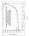
- FIG. 9is an exemplary solar cell I-V characteristics plot measured from a copper indium disulfide based thin film photovoltaic cell characterized by an interface region between an electrode layer and absorber layer substantially free from metal disulfide layer having a semiconductor characteristic that is different from the copper indium disulfide material according to an embodiment of the present invention.
- FIG. 10is an exemplary solar cell I-V characteristics plot measured from a copper indium disulfide based thin film photovoltaic cell characterized by an interface region between an electrode layer and absorber layer contaminated by metal disulfide layer having a semiconductor characteristic that is different from the copper indium disulfide material.
- the present inventionprovides a method for manufacturing thin film photovoltaic devices.
- the methodhas been used to provide a copper indium disulfide thin film material for high efficiency solar cell application.
- the present inventionhas a much broader range of applicability, for example, embodiments of the present invention may be used to form other semiconducting thin films or multilayers comprising iron sulfide, cadmium sulfide, zinc selenide, and others, and metal oxides such as zinc oxide, iron oxide, copper oxide, and others.
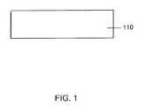
- FIG. 1is a schematic diagram illustrating a process of a method for forming a thin film photovoltaic device according to an embodiment of the present invention.
- the diagramis merely an example, which should not unduly limit the claims herein.
- a substrate 110is provided.
- the substrate 110includes a surface region 112 and is held in a process stage within a process chamber (not shown).
- the substrate 110is an optically transparent solid material.
- the substrate 110can be a glass, quartz, fused silica, or a plastic, or metal, or foil, or semiconductor, or other composite materials.
- the substratecan be a single material, multiple materials, which are layered, composites, or stacked, including combinations of these, and the like. Of course there can be other variations, modifications, and alternatives.
- FIG. 2is a schematic diagram illustrating a process of the method for forming a thin film photovoltaic device according to an embodiment of the present invention.
- the diagramis merely an example, which should not unduly limit the claims herein.
- the present inventionprovides a process for forming a thin film photovoltaic device is to form an electrode layer.
- an electrode layer 120is formed overlying the surface region 112 of the substrate 110 .
- the electrode layer 120can be made of molybdenum using sputtering, evaporation (e.g., electron beam), electro plating, combination of these, and the like according to a specific embodiment.
- the thickness of the electrode layercan be ranged from 100 nm to 2 micron and others, characterized by resistivity of about 100 Ohm/cm 2 to 10 Ohm/cm 2 and less according to a specific embodiment.
- the electrodeis made of molybdenum or tungsten, but can be others like copper, chromium, aluminum, nickel, or platinum. Of course, there can be other variations, modifications, and alternatives.
- FIG. 3is a schematic diagram illustrating a process of the method for forming a thin film photovoltaic device according to an embodiment of the present invention.
- the diagramis merely an example, which should not unduly limit the claims herein.
- a process of forming a copper layer overlying the electrode layer formed in last processis a process of forming a copper layer overlying the electrode layer formed in last process.
- a copper (Cu) layer 130is formed overlying the electrode layer 120 .
- the copper layeris formed using a sputtering process.
- a DC magnetron sputtering processcan be used to deposit Cu layer 130 onto the electrode layer 120 under a following condition.
- the deposition pressure(using Ar gas) is controlled to be about 6.2 mTorr.
- the gas flow rateis set to about 32 sccm.
- the deposition temperaturecan be just at room temperature without need of intentionally heating the substrate. Of course, minor heating may be resulted due to the plasma generated during the deposition. Additionally, the DC power supply of about 115 W may be required. According to certain embodiments, DC power in a range from 100 W to 150 W is suitable depending specific cases with different materials.
- the full deposition time for a Cu layer of 330 nm thicknessis about 6 minutes or more.
- the deposition conditioncan be varied and modified according to a specific embodiment.
- the sputtering process of Cucan be performed using a copper-gallium (Cu—Ga) alloy target. Therefore, the Cu layer 130 can contain at least partially a desirable and adjustable amount of Ga species within the final metal precursor film.
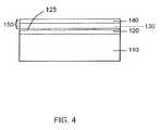
- the methodincludes forming a barrier layer 125 overlying the electrode layer to form an interface region between the electrode layer and the copper layer.
- the interface regionis maintained substantially free from metal disulfide layer having a semiconductor characteristic that is different from the copper indium disulfide material during later processing steps.
- the barrier layerhas suitable conductive characteristics and can be reflective to allow electromagnetic radiation to reflect back or can also be transparent or the like.
- the barrier layeris selected from platinum, titanium, chromium, or silver. Of course, there can be other variations, modifications, and alternatives.
- FIG. 4is a schematic diagram illustrating a process of the method for forming a thin film photovoltaic device according to an embodiment of the present invention.
- the diagramis merely an example, which should not unduly limit the claims herein.
- One skilled in the artwould recognize other variations, modifications, and alternatives.
- a process of providing an indium (In) layer overlying the copper layeris illustrated.
- the indium layer 140is formed overlying the copper layer 130 .
- the indium layeris deposited over the copper layer using a sputtering process.
- a DC magnetron sputtering processcan be used to deposit In layer 140 overlying the Cu layer 130 under a similar condition for depositing the Cu layer.
- the sputtering process to deposit In layer 140can be performed by using an In—Ga alloy target to form an In—Ga layer overlying the Cu layer 130 .
- the Ga contentcan be adjusted to a desired level by selecting a proper concentration ratio in the In—Ga alloy target and some deposition conditions. This Ga content at least partially contributes final Ga species and ratio of Cu/(In+Ga) within the metal precursor film for forming the absorber layer of the solar cell.
- the deposition time for the indium layermay be shorter than that for Cu layer. For example, 2 minutes and 45 seconds may be enough for depositing an In layer of about 410 nm in thickness according to a specific embodiment.
- the indium layeris provided overlying the copper layer by an electro plating process, or others dependent on specific embodiment.
- FIGS. 1 through 4illustrate a formation of a multilayered structure 150 comprising copper and indium on a transparent substrate provided by processes of a method of forming a thin film photovoltaic device.
- the copper layer 130 as well as the indium layer 140are provided with an stoichiometric control to ensure that the formed multilayered structure 150 is a Cu-rich material with an atomic ratio of Cu:In greater than 1 therein.
- the atomic ratio of Cu:Incan be in a range from 1.2:1 to 2.0:1 or larger depending upon the specific embodiment.
- the atomic ratio of Cu:Inis between 1.35:1 and 1.60:1.
- the atomic ratio of Cu:Inis between 1.4:1 and 1.60:1. In yet another example, the atomic ratio of Cu:In is selected to be about 1.5:1. In a preferred embodiment, the Cu:In is introduced copper rich, which consumes substantially all of the indium species, in the resulting structure. In a specific embodiment, the formation process of indium layer 140 substantially causes no change in atomic stoichiometry in the copper layer 130 formed earlier. In another specific embodiment, the formation process of the indium layer 140 is performed earlier overlying the electrode layer 120 while the formation process of the copper layer 130 is performed later overlying the indium layer 140 .
- FIG. 5is a schematic diagram illustrating a process of the method for forming a thin film photovoltaic device according to an embodiment of the present invention.
- the diagramis merely an example, which should not unduly limit the claims herein.
- the formed multilayered structure 150comprising at least an indium layer 140 over a copper layer 130 is subjected to a thermal treatment process 200 in an environment containing a sulfur bearing species 210 at an adequate pressure and at a temperature of about 400 Degrees Celsius to about 600 Degrees Celsius for about three to fifteen minutes for a rapid thermal process according to a specific embodiment.
- the sulfur bearing speciesare in a fluid phase.
- the sulfurcan be provided in a solution, which has dissolved Na 2 S, CS 2 , (NH 4 ) 2 S, thiosulfate, and others.
- the sulfur bearing species 210are hydrogen sulfide in gas phase.
- the sulfurcan be provided in a solid phase. In a solid phase, elemental sulfur can be heated and allowed to boil, which vaporizes into a gas phase, e.g., S. In a specific embodiment, the gas phase is allowed to react to the indium/copper layers. In other embodiments, other combinations of sulfur species can be used.
- the thermal treatment process 200includes certain predetermined ramp-up and ramp down period with certain predetermined speed for temperature changes.
- the thermal treatment processis a rapid thermal annealing process.
- the hydrogen sulfide gasis provided through one or more entry valves with flow rate control into the process chamber where the hydrogen sulfide gas pressure is under controlled by one or more pumps.
- entry valveswith flow rate control into the process chamber where the hydrogen sulfide gas pressure is under controlled by one or more pumps.
- the sulfurcan be provided as a layer overlying the indium and copper layers or copper and indium layers.
- the sulfur materialis provided as a thin layer or patterned layer.
- the sulfurcan be provided as a slurry, powder, solid material, gas, paste, or other suitable form.
- the thermal treatment process 200causes a reaction between copper indium material within the multilayered structure 150 and the sulfur bearing species 210 , thereby forming a layer of copper indium disulfide material (or a copper indium disulfide thin film) 220 .
- the copper indium disulfide material or copper indium disulfide thin film 220is transformed by incorporating sulfur ions/atoms stripped or decomposed from the sulfur bearing species into the multilayered structure 150 with indium atoms and copper atoms mutually diffused therein.
- the thermal treatment process 200would result in a formation of a cap layer over the transformed copper indium disulfide material 220 .
- the cap layercontains a thickness of substantially copper sulfide material 221 but substantially free of indium atoms.
- the copper sulfide material 221includes a surface region 225 of the same copper sulfide material substantially free of indium atoms.
- the formation of this cap layeris under a Cu-rich conditions for the original Cu—In bearing multilayered structure 150 .
- the thickness of the copper sulfide material 221is on an order of about five to ten nanometers and greater based on original multilayered structure 150 with indium layer 140 overlying copper layer 130 .
- FIG. 6is a schematic diagram illustrating a process of the method for forming a thin film photovoltaic device according to an embodiment of the present invention.
- the diagramis merely an example, which should not unduly limit the claims herein.
- a dip process 300is performed to the copper sulfide material 221 that covers the copper indium disulfide thin film 220 .
- the dip processis performed by exposing the surface region 225 to 1 to about 10 weight % solution of potassium cyanide 310 according to a specific embodiment.
- the potassium cyanideacts as an etchant that is capable of selectively removing copper sulfide material 221 .
- the etching processstarts from the exposed surface region 225 and down to the thickness of the copper sulfide material 221 and substantially stopped at the interface between the copper sulfide material 221 and copper indium disulfide material 220 .
- the copper sulfide cap layer 221is selectively removed by the etching process so that a new surface region 228 of the remaining copper indium disulfide thin film 220 is exposed according to a specific embodiment.
- the etch selectivityis about 1:100 or more between copper sulfide and copper indium disulfide.
- other selective etching speciescan be used.
- the etching speciescan be hydrogen peroxide.
- the copper sulfide materialcan be mechanically removed, chemically removed, electrically removed, or any combination of these, among others.
- the absorber layer made of copper indium disulfideis about 1 to 10 microns, but can be others. Of course, there can be other variations, modifications, and alternatives.
- FIG. 7is a schematic diagram illustrating a process of the method for forming a thin film photovoltaic device according to an embodiment of the present invention.
- the diagramis merely an example, which should not unduly limit the claims herein.
- One skilled in the artwould recognize other variations, modifications, and alternatives.
- a p-type copper indium disulfide film 320is formed.
- the previously-formed copper indium disulfide material 220has possessed a p-type semiconducting characteristic and is substantially the same as the p-type copper indium disulfide film 320 .
- the copper indium disulfide material 220is subjected to additional doping process to adjust p-type impurity density therein for the purpose of optimizing I-V characteristic of the high efficiency thin film photovoltaic devices.
- aluminum speciesare mixed into the copper indium disulfide material 220 .
- the copper indium disulfide material 220is mixed with a copper indium aluminum disulfide material to form the film 320 .
- a window layer 310is formed overlying the p-type copper indium disulfide material 320 .
- the window layer 310can be selected from a group materials consisting of a cadmium sulfide (CdS), a zinc sulfide (ZnS), zinc selenium (ZnSe), zinc oxide (ZnO), zinc magnesium oxide (ZnMgO), or others and may be doped with impurities for conductivity, e.g., n + type.
- the window layer 310is intended to serve another part of a PN-junction associated with a photovoltaic cell.
- the window layer 310is heavily doped to form a n + -type semiconductor layer.
- indium speciesare used as the doping material to cause formation of the n + -type characteristic associated with the window layer 310 .
- the doping processis performed using suitable conditions.
- ZnO window layer that is doped with aluminumcan range from about 200 to 500 nanometers.
- FIG. 8is a schematic diagram illustrating a process of the method for forming a thin film photovoltaic device according to an embodiment of the present invention.
- the diagramis merely an example, which should not unduly limit the claims herein.
- a conductive layer 330is added at least partially on top of the window layer 310 to form a top electrode layer for the photovoltaic device.
- the conductive layer 330is a transparent conductive oxide TCO layer.
- TCOcan be selected from a group consisting of In 2 O 3 :Sn (ITO), ZnO:Al (AZO), SnO 2 :F (TFO), and can be others.
- the formation of the TCO layeris followed a certain predetermined pattern for effectively carried out the function of top electrode layer for the photovoltaic device with considerations of maximizing the efficiency of the thin film based photovoltaic devices.
- the TCOcan also act as a window layer, which essentially eliminates a separate window layer.
- FIG. 9is an exemplary solar cell I-V characteristics plot measured from a copper indium disulfide based thin film photovoltaic cell characterized by an interface region between an electrode layer and absorber layer substantially free from metal disulfide layer having a semiconductor characteristic that is different from the copper indium disulfide material according to an embodiment of the present invention.
- the diagramis merely an example, which should not unduly limit the claims herein. One skilled in the art would recognize other variations, modifications, and alternatives.
- a current density of a high efficiency copper indium disulfide thin film photovoltaic cell made according to an embodiment of the present inventionis plotted against a bias voltage.
- the curveintersects the y-axis with a short circuit current value at about ⁇ 0.0235 A/cm 2 and intersects a zero current line with a bias at about 0.69 V.
- the corresponding photovoltaic cellhas an absorber layer made from copper indium disulfide thin film according to an embodiment of the present invention.
- the absorber layeris about 1.5 ⁇ m in thickness and an atomic ratio of Cu:In at about 1.5:1.
- an interface regionis maintained, during the cell formation processes according to embodiments of the present invention, substantially free from metal disulfide layer having a semiconductor characteristic that is different from the copper indium disulfide material. Based on standard formula, a cell conversion efficiency ⁇ can be estimated:
- J SCis the short circuit current density of the cell
- V OCis the open circuit bias voltage applied
- FFis the so-called fill factor defined as the ratio of the maximum power point divided by the open circuit voltage (Voc) and the short circuit current (J sc ).
- the input light irradiance (P in , in W/m 2 )under standard test conditions [i.e., STC that specifies a temperature of 25° C.
- FIG. 10is an exemplary solar cell I-V characteristics plot measured from a copper indium disulfide based thin film photovoltaic cell characterized by an interface region between an electrode layer and absorber layer contaminated by metal disulfide layer having a semiconductor characteristic that is different from the copper indium disulfide material.
- the diagramis merely an example, which should not unduly limit the claims herein. One skilled in the art would recognize other variations, modifications, and alternatives. As shown, the plot illustrates degradation due to contamination and/or imperfections at an interface region within the absorber material, which has been previously noted. As shown in FIG. 10 , a current density of a poor efficiency copper indium disulfide thin film photovoltaic cell is plotted against a bias voltage.
- the short circuit current valueis only about ⁇ 0.019 A/cm 2 and the open circuit voltage is about 0.66 V.
- the corresponding photovoltaic cellhas an absorber layer made from copper indium disulfide thin film substantially similar to the cell shown in FIG. 9 , although there are limitations with the cell of FIG. 10 .
- the absorber layeris about 1.5 ⁇ m in thickness and an atomic ratio of Cu:In at about 1.5:1.
- an interface regionis contaminated by metal disulfide layer having a semiconductor characteristic that is different from the copper indium disulfide material during the cell formation processes (without adding a proper barrier layer).
- the energy convert efficiencywhich can also be extracted using the I-V characteristic plot, is much poor with a value of about 6.7%, which illustrates an example of a limitation of the absorber material. Therefore, using the present barrier layer according to one or more embodiments of the present invention to form an interface region and maintaining the interface region substantially free from the metal contaminants that have a semiconductor characteristic that is different from the copper indium disulfide material provides a much improved technique for making high efficiency thin film photovoltaic cell.
- the present methodmaintains an interface region between the electrode layer overlying the surface region and the copper indium disulfide material substantially free from a metal disulfide layer having different semiconductor characteristics from the copper indium disulfide material.
- the metal disulfide layeris selected from molybdenum disulfide layer or the like.
- the interface regionis characterized by a surface morphology substantially preventing any formation of the metal disulfide layer, which is characterized by a thickness of about 5 to 10 nanometers.
- the present methodincludes a thermal process during at least the maintaining process or a portion of the maintaining process of at least 300 Degrees Celsius and greater to prevent any formation of the metal disulfide layer, which can be the molybdenum disulfide or like layer.
- a thermal processduring at least the maintaining process or a portion of the maintaining process of at least 300 Degrees Celsius and greater to prevent any formation of the metal disulfide layer, which can be the molybdenum disulfide or like layer.
Landscapes
- Engineering & Computer Science (AREA)
- Physics & Mathematics (AREA)
- Condensed Matter Physics & Semiconductors (AREA)
- General Physics & Mathematics (AREA)
- Manufacturing & Machinery (AREA)
- Computer Hardware Design (AREA)
- Microelectronics & Electronic Packaging (AREA)
- Power Engineering (AREA)
- Photovoltaic Devices (AREA)
- Life Sciences & Earth Sciences (AREA)
- Sustainable Energy (AREA)
Abstract
Description
where JSCis the short circuit current density of the cell, VOCis the open circuit bias voltage applied, FF is the so-called fill factor defined as the ratio of the maximum power point divided by the open circuit voltage (Voc) and the short circuit current (Jsc). The input light irradiance (Pin, in W/m2) under standard test conditions [i.e., STC that specifies a temperature of 25° C. and an irradiance of 1000 W/m2with an air mass 1.5 (AM1.5) spectrum.] and the surface area of the solar cell (in m2). Thus a 10.4% efficiency can be accurately estimated for this particular cell characterized by an interface region between an electrode layer and absorber layer substantially free from metal disulfide layer having a semiconductor characteristic that is different from the copper indium disulfide material according to embodiments of the present invention. In a specific embodiment, the bandgap is about 1.45 eV to 1.5 eV. Of course, there can be other variations, modifications, and alternatives.
Claims (20)
Priority Applications (4)
| Application Number | Priority Date | Filing Date | Title |
|---|---|---|---|
| US12/479,409US9087943B2 (en) | 2008-06-25 | 2009-06-05 | High efficiency photovoltaic cell and manufacturing method free of metal disulfide barrier material |
| CN2009801223023ACN102067278B (en) | 2008-06-25 | 2009-06-09 | High-efficiency photovoltaic cells and methods of fabrication without metal disulfide barrier materials |
| PCT/US2009/046802WO2009158187A1 (en) | 2008-06-25 | 2009-06-09 | High efficiency photovoltaic cell and manufacturing method free of metal disulfide barrier material |
| DE112009001334TDE112009001334T5 (en) | 2008-06-25 | 2009-06-09 | High efficiency photovoltaic cell and manufacturing process free of metal disulfide barrier material |
Applications Claiming Priority (2)
| Application Number | Priority Date | Filing Date | Title |
|---|---|---|---|
| US7533808P | 2008-06-25 | 2008-06-25 | |
| US12/479,409US9087943B2 (en) | 2008-06-25 | 2009-06-05 | High efficiency photovoltaic cell and manufacturing method free of metal disulfide barrier material |
Publications (2)
| Publication Number | Publication Date |
|---|---|
| US20090320920A1 US20090320920A1 (en) | 2009-12-31 |
| US9087943B2true US9087943B2 (en) | 2015-07-21 |
Family
ID=41444880
Family Applications (1)
| Application Number | Title | Priority Date | Filing Date |
|---|---|---|---|
| US12/479,409Expired - Fee RelatedUS9087943B2 (en) | 2008-06-25 | 2009-06-05 | High efficiency photovoltaic cell and manufacturing method free of metal disulfide barrier material |
Country Status (4)
| Country | Link |
|---|---|
| US (1) | US9087943B2 (en) |
| CN (1) | CN102067278B (en) |
| DE (1) | DE112009001334T5 (en) |
| WO (1) | WO2009158187A1 (en) |
Families Citing this family (4)
| Publication number | Priority date | Publication date | Assignee | Title |
|---|---|---|---|---|
| US20110017298A1 (en) | 2007-11-14 | 2011-01-27 | Stion Corporation | Multi-junction solar cell devices |
| US20100078059A1 (en) | 2008-09-30 | 2010-04-01 | Stion Corporation | Method and structure for thin film tandem photovoltaic cell |
| US8563850B2 (en) | 2009-03-16 | 2013-10-22 | Stion Corporation | Tandem photovoltaic cell and method using three glass substrate configuration |
| WO2011129979A2 (en)* | 2010-04-12 | 2011-10-20 | Applied Materials, Inc. | Method for depositing barrier layers on substrates for high quality films |
Citations (239)
| Publication number | Priority date | Publication date | Assignee | Title |
|---|---|---|---|---|
| US3520732A (en) | 1965-10-22 | 1970-07-14 | Matsushita Electric Industrial Co Ltd | Photovoltaic cell and process of preparation of same |
| US3828722A (en) | 1970-05-01 | 1974-08-13 | Cogar Corp | Apparatus for producing ion-free insulating layers |
| US3975211A (en) | 1975-03-28 | 1976-08-17 | Westinghouse Electric Corporation | Solar cells and method for making same |
| US4062038A (en) | 1976-01-28 | 1977-12-06 | International Business Machines Corporation | Radiation responsive device |
| US4263336A (en) | 1979-11-23 | 1981-04-21 | Motorola, Inc. | Reduced pressure induction heated reactor and method |
| US4332974A (en) | 1979-06-28 | 1982-06-01 | Chevron Research Company | Multilayer photovoltaic cell |
| US4335266A (en) | 1980-12-31 | 1982-06-15 | The Boeing Company | Methods for forming thin-film heterojunction solar cells from I-III-VI.sub.2 |
| DE3314197A1 (en) | 1982-04-28 | 1983-11-03 | Energy Conversion Devices, Inc., 48084 Troy, Mich. | P-CONDUCTING AMORPHOUS SILICON ALLOY WITH A LARGE BAND GAP AND MANUFACTURING PROCESS THEREFOR |
| US4441113A (en) | 1981-02-13 | 1984-04-03 | Energy Conversion Devices, Inc. | P-Type semiconductor material having a wide band gap |
| US4442310A (en) | 1982-07-15 | 1984-04-10 | Rca Corporation | Photodetector having enhanced back reflection |
| US4461922A (en) | 1983-02-14 | 1984-07-24 | Atlantic Richfield Company | Solar cell module |
| US4465575A (en) | 1981-09-21 | 1984-08-14 | Atlantic Richfield Company | Method for forming photovoltaic cells employing multinary semiconductor films |
| US4471155A (en) | 1983-04-15 | 1984-09-11 | Energy Conversion Devices, Inc. | Narrow band gap photovoltaic devices with enhanced open circuit voltage |
| US4499658A (en) | 1983-09-06 | 1985-02-19 | Atlantic Richfield Company | Solar cell laminates |
| US4507181A (en) | 1984-02-17 | 1985-03-26 | Energy Conversion Devices, Inc. | Method of electro-coating a semiconductor device |
| US4517403A (en) | 1983-05-16 | 1985-05-14 | Atlantic Richfield Company | Series connected solar cells and method of formation |
| US4518855A (en) | 1982-09-30 | 1985-05-21 | Spring-Mornne, Inc. | Method and apparatus for statically aligning shafts and monitoring shaft alignment |
| US4532372A (en) | 1983-12-23 | 1985-07-30 | Energy Conversion Devices, Inc. | Barrier layer for photovoltaic devices |
| US4542255A (en) | 1984-01-03 | 1985-09-17 | Atlantic Richfield Company | Gridded thin film solar cell |
| US4581108A (en) | 1984-01-06 | 1986-04-08 | Atlantic Richfield Company | Process of forming a compound semiconductive material |
| US4589194A (en) | 1983-12-29 | 1986-05-20 | Atlantic Richfield Company | Ultrasonic scribing of thin film solar cells |
| US4598306A (en) | 1983-07-28 | 1986-07-01 | Energy Conversion Devices, Inc. | Barrier layer for photovoltaic devices |
| US4599154A (en) | 1985-03-15 | 1986-07-08 | Atlantic Richfield Company | Electrically enhanced liquid jet processing |
| US4611091A (en) | 1984-12-06 | 1986-09-09 | Atlantic Richfield Company | CuInSe2 thin film solar cell with thin CdS and transparent window layer |
| US4623601A (en) | 1985-06-04 | 1986-11-18 | Atlantic Richfield Company | Photoconductive device containing zinc oxide transparent conductive layer |
| US4625070A (en) | 1985-08-30 | 1986-11-25 | Atlantic Richfield Company | Laminated thin film solar module |
| US4638111A (en) | 1985-06-04 | 1987-01-20 | Atlantic Richfield Company | Thin film solar cell module |
| US4661370A (en) | 1984-02-08 | 1987-04-28 | Atlantic Richfield Company | Electric discharge processing of thin films |
| US4663495A (en) | 1985-06-04 | 1987-05-05 | Atlantic Richfield Company | Transparent photovoltaic module |
| US4705912A (en) | 1985-09-27 | 1987-11-10 | Sanyo Electric Co., Ltd. | Photovoltaic device |
| US4724011A (en) | 1983-05-16 | 1988-02-09 | Atlantic Richfield Company | Solar cell interconnection by discrete conductive regions |
| US4727047A (en) | 1980-04-10 | 1988-02-23 | Massachusetts Institute Of Technology | Method of producing sheets of crystalline material |
| US4751149A (en) | 1985-06-04 | 1988-06-14 | Atlantic Richfield Company | Chemical vapor deposition of zinc oxide films and products |
| US4775425A (en) | 1987-07-27 | 1988-10-04 | Energy Conversion Devices, Inc. | P and n-type microcrystalline semiconductor alloy material including band gap widening elements, devices utilizing same |
| US4793283A (en) | 1987-12-10 | 1988-12-27 | Sarkozy Robert F | Apparatus for chemical vapor deposition with clean effluent and improved product yield |
| US4798660A (en) | 1985-07-16 | 1989-01-17 | Atlantic Richfield Company | Method for forming Cu In Se2 films |
| US4816082A (en) | 1987-08-19 | 1989-03-28 | Energy Conversion Devices, Inc. | Thin film solar cell including a spatially modulated intrinsic layer |
| US4865999A (en) | 1987-07-08 | 1989-09-12 | Glasstech Solar, Inc. | Solar cell fabrication method |
| US4873118A (en) | 1988-11-18 | 1989-10-10 | Atlantic Richfield Company | Oxygen glow treating of ZnO electrode for thin film silicon solar cell |
| US4915745A (en) | 1988-09-22 | 1990-04-10 | Atlantic Richfield Company | Thin film solar cell and method of making |
| US4950615A (en) | 1989-02-06 | 1990-08-21 | International Solar Electric Technology, Inc. | Method and making group IIB metal - telluride films and solar cells |
| US4968354A (en) | 1987-11-09 | 1990-11-06 | Fuji Electric Co., Ltd. | Thin film solar cell array |
| US4996108A (en) | 1989-01-17 | 1991-02-26 | Simon Fraser University | Sheets of transition metal dichalcogenides |
| US5008062A (en) | 1988-01-20 | 1991-04-16 | Siemens Solar Industries, L.P. | Method of fabricating photovoltaic module |
| US5011565A (en) | 1989-12-06 | 1991-04-30 | Mobil Solar Energy Corporation | Dotted contact solar cell and method of making same |
| US5028274A (en) | 1989-06-07 | 1991-07-02 | International Solar Electric Technology, Inc. | Group I-III-VI2 semiconductor films for solar cell application |
| US5039353A (en) | 1989-04-27 | 1991-08-13 | Societe Dite: Solems (Societe Anonyme) | Process for improving the spectral response of a photoconductive structure, and improved solar cell and photoreceptive structure |
| US5045409A (en) | 1987-11-27 | 1991-09-03 | Atlantic Richfield Company | Process for making thin film solar cell |
| US5069727A (en) | 1989-09-06 | 1991-12-03 | Sanyo Electric Co., Ltd. | Flexible photovoltaic device and manufacturing method thereof |
| US5078803A (en) | 1989-09-22 | 1992-01-07 | Siemens Solar Industries L.P. | Solar cells incorporating transparent electrodes comprising hazy zinc oxide |
| US5125984A (en) | 1990-05-31 | 1992-06-30 | Siemens Aktiengesellschaft | Induced junction chalcopyrite solar cell |
| US5133809A (en) | 1989-10-07 | 1992-07-28 | Showa Shell Sekiyu K.K. | Photovoltaic device and process for manufacturing the same |
| US5137835A (en) | 1990-07-24 | 1992-08-11 | Siemens Aktiengesellschaft | Method for manufacturing a chalcopyrite solar cell |
| US5154777A (en) | 1990-02-26 | 1992-10-13 | Mcdonnell Douglas Corporation | Advanced survivable space solar power system |
| US5180686A (en) | 1988-10-31 | 1993-01-19 | Energy Conversion Devices, Inc. | Method for continuously deposting a transparent oxide material by chemical pyrolysis |
| US5211824A (en) | 1991-10-31 | 1993-05-18 | Siemens Solar Industries L.P. | Method and apparatus for sputtering of a liquid |
| US5217564A (en) | 1980-04-10 | 1993-06-08 | Massachusetts Institute Of Technology | Method of producing sheets of crystalline material and devices made therefrom |
| US5231047A (en) | 1991-12-19 | 1993-07-27 | Energy Conversion Devices, Inc. | High quality photovoltaic semiconductor material and laser ablation method of fabrication same |
| US5248345A (en) | 1990-10-17 | 1993-09-28 | Showa Shell Sekiyu K.K. | Integrated photovoltaic device |
| US5259883A (en) | 1988-02-16 | 1993-11-09 | Kabushiki Kaisha Toshiba | Method of thermally processing semiconductor wafers and an apparatus therefor |
| US5261968A (en) | 1992-01-13 | 1993-11-16 | Photon Energy, Inc. | Photovoltaic cell and method |
| US5298086A (en) | 1992-05-15 | 1994-03-29 | United Solar Systems Corporation | Method for the manufacture of improved efficiency tandem photovoltaic device and device manufactured thereby |
| US5336623A (en) | 1992-03-02 | 1994-08-09 | Showa Shell Sekiyu K.K. | Process for producing integrated solar cell |
| US5346853A (en) | 1992-06-29 | 1994-09-13 | United Solar Systems Corporation | Microwave energized deposition process with substrate temperature control for the fabrication of P-I-N photovoltaic devices |
| US5397401A (en) | 1992-06-29 | 1995-03-14 | Canon Kabushiki Kaisha | Semiconductor apparatus covered with a sealing resin composition |
| US5399504A (en) | 1991-05-08 | 1995-03-21 | Fuji Electric Corporate Research & Development Ltd. | Method of manufacturing CuInSe2 thin film solar cell |
| US5436204A (en) | 1993-04-12 | 1995-07-25 | Midwest Research Institute | Recrystallization method to selenization of thin-film Cu(In,Ga)Se2 for semiconductor device applications |
| US5445847A (en) | 1992-05-19 | 1995-08-29 | Matsushita Electric Industrial Co., Ltd. | Method for preparing chalcopyrite-type compound |
| US5474939A (en) | 1992-12-30 | 1995-12-12 | Siemens Solar Industries International | Method of making thin film heterojunction solar cell |
| US5501744A (en) | 1992-01-13 | 1996-03-26 | Photon Energy, Inc. | Photovoltaic cell having a p-type polycrystalline layer with large crystals |
| US5512107A (en) | 1992-03-19 | 1996-04-30 | Siemens Solar Gmbh | Environmentally stable thin-film solar module |
| US5528397A (en) | 1991-12-03 | 1996-06-18 | Kopin Corporation | Single crystal silicon transistors for display panels |
| US5536333A (en) | 1992-05-12 | 1996-07-16 | Solar Cells, Inc. | Process for making photovoltaic devices and resultant product |
| US5578503A (en)* | 1992-09-22 | 1996-11-26 | Siemens Aktiengesellschaft | Rapid process for producing a chalcopyrite semiconductor on a substrate |
| US5578103A (en) | 1994-08-17 | 1996-11-26 | Corning Incorporated | Alkali metal ion migration control |
| US5622634A (en) | 1993-12-17 | 1997-04-22 | Canon Kabushiki Kaisha | Method of manufacturing electron-emitting device, electron source and image-forming apparatus |
| US5626688A (en) | 1994-12-01 | 1997-05-06 | Siemens Aktiengesellschaft | Solar cell with chalcopyrite absorber layer |
| US5665175A (en) | 1990-05-30 | 1997-09-09 | Safir; Yakov | Bifacial solar cell |
| US5676766A (en) | 1993-09-30 | 1997-10-14 | Siemens Aktiengesellschaft | Solar cell having a chalcopyrite absorber layer |
| US5726065A (en) | 1995-02-21 | 1998-03-10 | Imec Vzw | Method of preparing solar cell front contacts |
| US5738731A (en) | 1993-11-19 | 1998-04-14 | Mega Chips Corporation | Photovoltaic device |
| US5858819A (en) | 1994-06-15 | 1999-01-12 | Seiko Epson Corporation | Fabrication method for a thin film semiconductor device, the thin film semiconductor device itself, liquid crystal display, and electronic device |
| US5868869A (en) | 1995-06-07 | 1999-02-09 | Photon Energy, Inc. | Thin film photovoltaic device and process of manufacture |
| US5977476A (en) | 1996-10-16 | 1999-11-02 | United Solar Systems Corporation | High efficiency photovoltaic device |
| US5981868A (en) | 1996-10-25 | 1999-11-09 | Showa Shell Sekiyu K.K. | Thin-film solar cell comprising thin-film light absorbing layer of chalcopyrite multi-element compound semiconductor |
| US5985691A (en) | 1997-05-16 | 1999-11-16 | International Solar Electric Technology, Inc. | Method of making compound semiconductor films and making related electronic devices |
| US6040521A (en) | 1996-11-08 | 2000-03-21 | Showa Shell Sekiyu K.K. | N-type window layer for a thin film solar cell and method of making |
| US6048442A (en) | 1996-10-25 | 2000-04-11 | Showa Shell Sekiyu K.K. | Method for producing thin-film solar cell and equipment for producing the same |
| JP2000173969A (en) | 1998-12-03 | 2000-06-23 | Canon Inc | Rinse method and photovoltaic device |
| JP2000219512A (en) | 1998-11-24 | 2000-08-08 | Canon Inc | Method for manufacturing zinc oxide thin film, method for manufacturing photovoltaic device using the same, and photovoltaic device |
| US6107562A (en) | 1998-03-24 | 2000-08-22 | Matsushita Electric Industrial Co., Ltd. | Semiconductor thin film, method for manufacturing the same, and solar cell using the same |
| US6127202A (en) | 1998-07-02 | 2000-10-03 | International Solar Electronic Technology, Inc. | Oxide-based method of making compound semiconductor films and making related electronic devices |
| US6160215A (en) | 1999-03-26 | 2000-12-12 | Curtin; Lawrence F. | Method of making photovoltaic device |
| US6166319A (en) | 1997-08-01 | 2000-12-26 | Canon Kabushiki Kaisha | Multi-junction photovoltaic device with microcrystalline I-layer |
| US6172297B1 (en) | 1997-09-23 | 2001-01-09 | Institut Fur Solarenergieforschung Gmbh | Solar cell and method for fabrication of a solar cell |
| US6258620B1 (en) | 1997-10-15 | 2001-07-10 | University Of South Florida | Method of manufacturing CIGS photovoltaic devices |
| WO2001057932A1 (en) | 2000-02-07 | 2001-08-09 | Cis Solartechnik Gmbh | Flexible metal substrate for cis solar cells, and method for producing the same |
| US6294274B1 (en) | 1998-11-16 | 2001-09-25 | Tdk Corporation | Oxide thin film |
| US6307148B1 (en) | 1999-03-29 | 2001-10-23 | Shinko Electric Industries Co., Ltd. | Compound semiconductor solar cell and production method thereof |
| US6323417B1 (en) | 1998-09-29 | 2001-11-27 | Lockheed Martin Corporation | Method of making I-III-VI semiconductor materials for use in photovoltaic cells |
| US6328871B1 (en) | 1999-08-16 | 2001-12-11 | Applied Materials, Inc. | Barrier layer for electroplating processes |
| US20020004302A1 (en) | 1995-09-14 | 2002-01-10 | Yoshihiko Fukumoto | Method for fabricating semiconductor device |
| US20020002992A1 (en) | 1998-06-30 | 2002-01-10 | Toshimitsu Kariya | Photovoltaic element |
| US6361718B1 (en) | 1998-02-05 | 2002-03-26 | Nippon Sheet Glass Co., Ltd. | Article having uneven surface, production process for the article, and composition for the process |
| US6372538B1 (en) | 2000-03-16 | 2002-04-16 | University Of Delaware | Fabrication of thin-film, flexible photovoltaic module |
| US20020061361A1 (en) | 2000-09-06 | 2002-05-23 | Hiroki Nakahara | Method and apparatus for fabricating electro-optical device and method and apparatus for fabricating liquid crystal panel |
| US20020063065A1 (en) | 2000-09-19 | 2002-05-30 | Yuichi Sonoda | Method of forming zinc oxide film and process for producing photovoltaic device using it |
| JP2002167695A (en) | 2000-09-19 | 2002-06-11 | Canon Inc | Method for forming zinc oxide film and method for manufacturing photovoltaic element using the same |
| US6423565B1 (en) | 2000-05-30 | 2002-07-23 | Kurt L. Barth | Apparatus and processes for the massproduction of photovotaic modules |
| DE10104726A1 (en) | 2001-02-02 | 2002-08-08 | Siemens Solar Gmbh | Process for structuring an oxide layer applied to a carrier material |
| JP2002270871A (en) | 2001-03-12 | 2002-09-20 | Canon Inc | Semiconductor element and method of forming silicon-based thin film |
| JP2002299670A (en) | 2001-04-03 | 2002-10-11 | Canon Inc | Silicon based thin film and photovoltaic device |
| US6500733B1 (en)* | 2001-09-20 | 2002-12-31 | Heliovolt Corporation | Synthesis of layers, coatings or films using precursor layer exerted pressure containment |
| US20030075717A1 (en) | 2001-03-12 | 2003-04-24 | Takaharu Kondo | Semiconductor element, and method of forming silicon-based film |
| US20030089899A1 (en) | 2000-08-22 | 2003-05-15 | Lieber Charles M. | Nanoscale wires and related devices |
| US20030188777A1 (en) | 2002-01-25 | 2003-10-09 | Konarka Technologies, Inc. | Co-sensitizers for dye sensitized solar cells |
| US6632113B1 (en) | 1998-09-09 | 2003-10-14 | Canon Kabushiki Kaisha | Image display apparatus, disassembly processing method therefor, and component recovery method |
| US6635307B2 (en) | 2001-12-12 | 2003-10-21 | Nanotek Instruments, Inc. | Manufacturing method for thin-film solar cells |
| US6653701B1 (en) | 1999-03-09 | 2003-11-25 | Fuji Xerox Co., Ltd. | Semiconductor device and production method thereof |
| US20030230338A1 (en) | 2002-06-17 | 2003-12-18 | Shalini Menezes | Thin film solar cell configuration and fabrication method |
| US6667492B1 (en) | 1997-11-10 | 2003-12-23 | Don L. Kendall | Quantum ridges and tips |
| US6690041B2 (en) | 2002-05-14 | 2004-02-10 | Global Solar Energy, Inc. | Monolithically integrated diodes in thin-film photovoltaic devices |
| US6692820B2 (en) | 1998-08-19 | 2004-02-17 | The Trustees Of Princeton University | Organic photosensitive optoelectronic device with a charge blocking layer |
| US20040063320A1 (en) | 2002-09-30 | 2004-04-01 | Hollars Dennis R. | Manufacturing apparatus and method for large-scale production of thin-film solar cells |
| US20040084080A1 (en) | 2002-06-22 | 2004-05-06 | Nanosolar, Inc. | Optoelectronic device and fabrication method |
| US20040095658A1 (en) | 2002-09-05 | 2004-05-20 | Nanosys, Inc. | Nanocomposites |
| US6784492B1 (en) | 1991-03-18 | 2004-08-31 | Canon Kabushiki Kaisha | Semiconductor device including a gate-insulated transistor |
| US20040187917A1 (en) | 2003-03-29 | 2004-09-30 | Nanosolar, Inc. | Transparent electrode, optoelectronic apparatus and devices |
| JP2004332043A (en) | 2003-05-07 | 2004-11-25 | Canon Inc | Method and apparatus for forming zinc oxide thin film, and method for forming photovoltaic element |
| US20040245912A1 (en) | 2003-04-01 | 2004-12-09 | Innovalight | Phosphor materials and illumination devices made therefrom |
| US20040252488A1 (en) | 2003-04-01 | 2004-12-16 | Innovalight | Light-emitting ceiling tile |
| US20040256001A1 (en) | 2002-12-17 | 2004-12-23 | General Electric Company | Photovoltaic cell using stable cu2o nanocrystals and conductive polymers |
| WO2005011002A1 (en) | 2003-07-24 | 2005-02-03 | Kaneka Corporation | Silicon based thin film solar cell |
| US6852920B2 (en) | 2002-06-22 | 2005-02-08 | Nanosolar, Inc. | Nano-architected/assembled solar electricity cell |
| US20050074915A1 (en) | 2001-07-13 | 2005-04-07 | Tuttle John R. | Thin-film solar cell fabricated on a flexible metallic substrate |
| US6878871B2 (en) | 2002-09-05 | 2005-04-12 | Nanosys, Inc. | Nanostructure and nanocomposite based compositions and photovoltaic devices |
| US20050098205A1 (en) | 2003-05-21 | 2005-05-12 | Nanosolar, Inc. | Photovoltaic devices fabricated from insulating nanostructured template |
| US20050164432A1 (en) | 2000-08-22 | 2005-07-28 | President And Fellows Of Harvard College | Doped elongated semiconductors, growing such semiconductors, devices including such semiconductors and fabricating such devices |
| US20050194036A1 (en) | 2004-03-01 | 2005-09-08 | Basol Bulent M. | Low cost and high throughput deposition methods and apparatus for high density semiconductor film growth |
| JP2005311292A (en) | 2004-03-25 | 2005-11-04 | Kaneka Corp | Substrate for thin film solar cell, manufacturing method therefor, and thin film solar cell using the same |
| US20050287717A1 (en) | 2004-06-08 | 2005-12-29 | Nanosys, Inc. | Methods and devices for forming nanostructure monolayers and devices including such monolayers |
| US20060034065A1 (en) | 2004-08-10 | 2006-02-16 | Innovalight, Inc. | Light strips for lighting and backlighting applications |
| US20060040103A1 (en) | 2004-06-08 | 2006-02-23 | Nanosys, Inc. | Post-deposition encapsulation of nanostructures: compositions, devices and systems incorporating same |
| US20060051505A1 (en) | 2004-06-18 | 2006-03-09 | Uwe Kortshagen | Process and apparatus for forming nanoparticles using radiofrequency plasmas |
| US20060096537A1 (en) | 2004-11-10 | 2006-05-11 | Daystar Technologies, Inc. | Method and apparatus for forming a thin-film solar cell using a continuous process |
| US20060096536A1 (en) | 2004-11-10 | 2006-05-11 | Daystar Technologies, Inc. | Pressure control system in a photovoltaic substrate deposition apparatus |
| US20060096635A1 (en) | 2004-11-10 | 2006-05-11 | Daystar Technologies, Inc. | Pallet based system for forming thin-film solar cells |
| US20060112983A1 (en) | 2004-11-17 | 2006-06-01 | Nanosys, Inc. | Photoactive devices and components with enhanced efficiency |
| US20060130890A1 (en) | 2004-12-20 | 2006-06-22 | Palo Alto Research Center Incorporated. | Heterojunction photovoltaic cell |
| US20060160261A1 (en) | 2005-01-20 | 2006-07-20 | Nanosolar, Inc. | Series interconnected optoelectronic device module assembly |
| US20060173113A1 (en) | 2005-02-01 | 2006-08-03 | Nippon Paint Co., Ltd. | Powder coating composition and coating method of aluminum wheel |
| US20060174932A1 (en) | 2003-07-14 | 2006-08-10 | Hiroki Usui | Electrolyte compositon, photoelectric converter and dye-sensitized solar cell using same |
| US20060219288A1 (en) | 2004-11-10 | 2006-10-05 | Daystar Technologies, Inc. | Process and photovoltaic device using an akali-containing layer |
| US20060220059A1 (en) | 2003-04-09 | 2006-10-05 | Matsushita Electric Industrial Co., Ltd | Solar cell |
| US20060219547A1 (en) | 2004-11-10 | 2006-10-05 | Daystar Technologies, Inc. | Vertical production of photovoltaic devices |
| US7122398B1 (en) | 2004-03-25 | 2006-10-17 | Nanosolar, Inc. | Manufacturing of optoelectronic devices |
| US20060249202A1 (en) | 2004-09-20 | 2006-11-09 | Seunghyup Yoo | Photovoltaic cell |
| WO2006126598A1 (en) | 2005-05-27 | 2006-11-30 | Showa Shell Sekiyu K.K. | Method for continuously depositing high resistance buffer layer/window layer (transparent conductive film) of cis based thin film solar cell and continuous film deposition equipment for carrying out that method |
| US20060267054A1 (en) | 2002-02-05 | 2006-11-30 | Peter Martin | Image sensor with microcrystalline germanium photodiode layer |
| US20070006914A1 (en) | 2004-06-18 | 2007-01-11 | Lee Howard W | Nanostructured materials and photovoltaic devices including nanostructured materials |
| US7179677B2 (en) | 2003-09-03 | 2007-02-20 | Midwest Research Institute | ZnO/Cu(InGa)Se2 solar cells prepared by vapor phase Zn doping |
| WO2007022221A2 (en)* | 2005-08-16 | 2007-02-22 | Nanosolar, Inc. | Photovolatic devices with conductive barrier layers and foil substrates |
| US7194197B1 (en) | 2000-03-16 | 2007-03-20 | Global Solar Energy, Inc. | Nozzle-based, vapor-phase, plume delivery structure for use in production of thin-film deposition layer |
| US20070093006A1 (en)* | 2005-10-24 | 2007-04-26 | Basol Bulent M | Technique For Preparing Precursor Films And Compound Layers For Thin Film Solar Cell Fabrication And Apparatus Corresponding Thereto |
| US20070089782A1 (en) | 2003-10-02 | 2007-04-26 | Scheuten Glasgroep | Spherical or grain-shaped semiconductor element for use in solar cells and method for producing the same; method for producing a solar cell comprising said semiconductor element and solar cell |
| US20070116892A1 (en) | 2005-11-18 | 2007-05-24 | Daystar Technologies, Inc. | Methods and apparatus for treating a work piece with a vaporous element |
| US7235736B1 (en) | 2006-03-18 | 2007-06-26 | Solyndra, Inc. | Monolithic integration of cylindrical solar cells |
| US20070151596A1 (en) | 2004-02-20 | 2007-07-05 | Sharp Kabushiki Kaisha | Substrate for photoelectric conversion device, photoelectric conversion device, and stacked photoelectric conversion device |
| WO2007077171A2 (en) | 2005-12-28 | 2007-07-12 | Sulfurcell Solartechnik Gmbh | Method and device for converting metallic precursors into chalcopyrite layers of cigss solar cells |
| US20070163643A1 (en) | 2004-02-19 | 2007-07-19 | Nanosolar, Inc. | High-throughput printing of chalcogen layer and the use of an inter-metallic material |
| US20070169810A1 (en) | 2004-02-19 | 2007-07-26 | Nanosolar, Inc. | High-throughput printing of semiconductor precursor layer by use of chalcogen-containing vapor |
| US7252923B2 (en) | 2001-10-16 | 2007-08-07 | Dai Nippon Printing Co., Ltd. | Methods for producing pattern-forming body |
| US20070193623A1 (en) | 2006-02-22 | 2007-08-23 | Guardian Industries Corp. | Electrode structure for use in electronic device and method of making same |
| US7265037B2 (en) | 2003-06-20 | 2007-09-04 | The Regents Of The University Of California | Nanowire array and nanowire solar cells and methods for forming the same |
| US20070209700A1 (en) | 2004-04-28 | 2007-09-13 | Honda Motor Co., Ltd. | Chalcopyrite Type Solar Cell |
| US20070264488A1 (en) | 2006-05-15 | 2007-11-15 | Stion Corporation | Method and structure for thin film photovoltaic materials using semiconductor materials |
| US20070283998A1 (en) | 2004-12-28 | 2007-12-13 | Showa Shell Sekiyu K.K. | Precursor Film And Method Of Forming The Same |
| US20070289624A1 (en) | 2004-08-09 | 2007-12-20 | Showa Shell Sekiyu K.K. | Cis Compound Semiconductor Thin-Film Solar Cell and Method of Forming Light Absorption Layer of the Solar Cell |
| US20080029154A1 (en) | 2006-08-04 | 2008-02-07 | Erel Milshtein | System and method for creating electric isolation between layers comprising solar cells |
| US20080032044A1 (en) | 2004-12-28 | 2008-02-07 | Showa Shell Sekiyu K.K. | Process For Producing Zno Transparent Conductive Film By Mocvd (Metal-Organic Chemical Vapor Deposition) Method |
| US20080041446A1 (en) | 2006-08-09 | 2008-02-21 | Industrial Technology Research Institute | Dye-sensitized solar cells and method for fabricating same |
| US20080057616A1 (en) | 2006-06-12 | 2008-03-06 | Robinson Matthew R | Bandgap grading in thin-film devices via solid group iiia particles |
| WO2008025326A2 (en) | 2006-09-01 | 2008-03-06 | Cis Solartechnik Gmbh & Co. Kg | Solar cell, method for manufacturing solar cells and electric conductor track |
| US20080092954A1 (en) | 2005-01-12 | 2008-04-24 | In-Solar Tech. Co. Ltd. | Optical Absorber Layers For Solar Cell And Method Of Manufacturing The Same |
| US20080092945A1 (en) | 2006-10-24 | 2008-04-24 | Applied Quantum Technology Llc | Semiconductor Grain and Oxide Layer for Photovoltaic Cells |
| US20080092953A1 (en) | 2006-05-15 | 2008-04-24 | Stion Corporation | Method and structure for thin film photovoltaic materials using bulk semiconductor materials |
| US7364808B2 (en) | 2001-10-19 | 2008-04-29 | Asahi Glass Company, Limited | Substrate with transparent conductive oxide film, process for its production and photoelectric conversion element |
| US20080105294A1 (en) | 2004-12-22 | 2008-05-08 | Showa Shell Sekiyu K.K. | Cis Type Thin-Film Photovoltaic Module, Process for Producing the Photovoltaic Module, and Method of Separating the Module |
| US20080110495A1 (en) | 2004-12-28 | 2008-05-15 | Showa Shell Sekiyu K.K. | Method for Forming Light Absorption Layer of Cis Type Thin-Film Solar Cell |
| US20080121264A1 (en) | 2006-11-28 | 2008-05-29 | Industrial Technology Research Institute | Thin film solar module and method of fabricating the same |
| US20080121277A1 (en) | 2004-02-19 | 2008-05-29 | Robinson Matthew R | High-throughput printing of semiconductor precursor layer from chalcogenide microflake particles |
| US20080204696A1 (en) | 2007-02-28 | 2008-08-28 | Tdk Corporation | Method of alignment |
| US20080210303A1 (en) | 2006-11-02 | 2008-09-04 | Guardian Industries Corp. | Front electrode for use in photovoltaic device and method of making same |
| US20080280030A1 (en) | 2007-01-31 | 2008-11-13 | Van Duren Jeoren K J | Solar cell absorber layer formed from metal ion precursors |
| US20080283389A1 (en) | 2004-05-11 | 2008-11-20 | Honda Motor Co., Ltd. | Method for Manufacturing Chalcopyrite Thin-Film Solar Cell |
| US20090021157A1 (en) | 2007-07-18 | 2009-01-22 | Tae-Woong Kim | Organic light emitting display and method of manufacturing the same |
| US20090058295A1 (en) | 2005-08-23 | 2009-03-05 | Saint-Gobain Glass France | Flat coplanar-discharge lamp and uses of same |
| US20090087942A1 (en) | 2005-08-05 | 2009-04-02 | Meyers Peter V | Manufacture of Photovoltaic Devices |
| US20090217969A1 (en) | 2005-10-31 | 2009-09-03 | Rohm Co., Ltd. | Method for Manufacturing Photoelectric Converter and Photoelectric Converter |
| US20090234987A1 (en) | 2008-03-12 | 2009-09-17 | Mips Technologies, Inc. | Efficient, Scalable and High Performance Mechanism for Handling IO Requests |
| US20090235983A1 (en) | 2008-03-18 | 2009-09-24 | Applied Quantum Technology, Llc | Interlayer Design for Epitaxial Growth of Semiconductor Layers |
| US20090235987A1 (en) | 2008-03-24 | 2009-09-24 | Epv Solar, Inc. | Chemical Treatments to Enhance Photovoltaic Performance of CIGS |
| US20090293945A1 (en) | 2008-06-02 | 2009-12-03 | Saint Gobain Glass France | Photovoltaic cell and photovoltaic cell substrate |
| US20100081230A1 (en) | 2008-09-30 | 2010-04-01 | Stion Corporation | Method and structure for adhesion of absorber material for thin film photovoltaic cell |
| US20100087016A1 (en) | 2008-04-15 | 2010-04-08 | Global Solar Energy, Inc. | Apparatus and methods for manufacturing thin-film solar cells |
| US20100087026A1 (en) | 2006-12-21 | 2010-04-08 | Helianthos B.V. | Method for making solar sub-cells from a solar cell |
| US20100096007A1 (en) | 2007-07-27 | 2010-04-22 | Saint-Gobain Glass France | Photovoltaic cell front face substrate and use of a substrate for a photovoltaic cell front face |
| US20100101649A1 (en) | 2006-11-14 | 2010-04-29 | Saint-Gobain Glass France | Porous layer, its manufacturing process and its applications |
| US20100101648A1 (en) | 2007-10-19 | 2010-04-29 | Sony Corporation | Dye-sensitized photoelectric conversion device and method of manufacturing the same |
| US20100122726A1 (en) | 2008-11-20 | 2010-05-20 | Stion Corporation | Method and structure for thin film photovoltaic cell using similar material junction |
| US7736755B2 (en) | 2005-04-25 | 2010-06-15 | Fujifilm Corporation | Organic electroluminescent device |
| US7741560B2 (en) | 2005-07-22 | 2010-06-22 | Honda Motor Co., Ltd. | Chalcopyrite solar cell |
| US20100197051A1 (en) | 2009-02-04 | 2010-08-05 | Applied Materials, Inc. | Metrology and inspection suite for a solar production line |
| US20100210064A1 (en) | 2008-05-19 | 2010-08-19 | Showa Shell Sekiyu K.K. | Method for manufacturing cis-based thin film solar cell |
| US20100233386A1 (en) | 2009-03-12 | 2010-09-16 | International Business Machines Corporation | Precision separation of pv thin film stacks |
| US20100258179A1 (en) | 2008-09-30 | 2010-10-14 | Stion Corporation | Thin film sodium species barrier method and structure for cigs based thin film photovoltaic cell |
| US20100267190A1 (en) | 2007-11-30 | 2010-10-21 | Hideki Hakuma | Laminated structure for cis based solar cell, and integrated structure and manufacturing method for cis based thin-film solar cell |
| US7855089B2 (en) | 2008-09-10 | 2010-12-21 | Stion Corporation | Application specific solar cell and method for manufacture using thin film photovoltaic materials |
| US7863074B2 (en) | 2008-09-30 | 2011-01-04 | Stion Corporation | Patterning electrode materials free from berm structures for thin film photovoltaic cells |
| US20110018103A1 (en) | 2008-10-02 | 2011-01-27 | Stion Corporation | System and method for transferring substrates in large scale processing of cigs and/or cis devices |
| US20110020980A1 (en) | 2008-10-01 | 2011-01-27 | Stion Corporation | Thermal pre-treatment process for soda lime glass substrate for thin film photovoltaic materials |
| US7910399B1 (en) | 2008-09-30 | 2011-03-22 | Stion Corporation | Thermal management and method for large scale processing of CIS and/or CIGS based thin films overlying glass substrates |
| US7998762B1 (en) | 2007-11-14 | 2011-08-16 | Stion Corporation | Method and system for large scale manufacture of thin film photovoltaic devices using multi-chamber configuration |
| US8003430B1 (en) | 2008-10-06 | 2011-08-23 | Stion Corporation | Sulfide species treatment of thin film photovoltaic cell and manufacturing method |
| US20110203634A1 (en) | 2010-01-22 | 2011-08-25 | Stion Corporation | Method and Structure for Tiling Industrial Thin-Film Solar Devices |
| US8008111B1 (en) | 2008-09-29 | 2011-08-30 | Stion Corporation | Bulk copper species treatment of thin film photovoltaic cell and manufacturing method |
| US8008110B1 (en) | 2008-09-29 | 2011-08-30 | Stion Corporation | Bulk sodium species treatment of thin film photovoltaic cell and manufacturing method |
| US8008112B1 (en) | 2008-09-29 | 2011-08-30 | Stion Corporation | Bulk chloride species treatment of thin film photovoltaic cell and manufacturing method |
| US20110212565A1 (en) | 2008-09-30 | 2011-09-01 | Stion Corporation | Humidity Control and Method for Thin Film Photovoltaic Materials |
| US20110259413A1 (en) | 2010-04-21 | 2011-10-27 | Stion Corporation | Hazy Zinc Oxide Film for Shaped CIGS/CIS Solar Cells |
| US20110259395A1 (en) | 2010-04-21 | 2011-10-27 | Stion Corporation | Single Junction CIGS/CIS Solar Module |
| US20110269260A1 (en) | 2008-06-25 | 2011-11-03 | Stion Corporation | Consumable Adhesive Layer for Thin Film Photovoltaic Material |
| US20110277836A1 (en) | 2007-09-28 | 2011-11-17 | Stion Corporation | Column structure thin film material using metal oxide bearing semiconductor material for solar cell devices |
| US20120003789A1 (en) | 2010-03-29 | 2012-01-05 | Stion Corporation | Apparatus for Manufacturing Thin Film Photovoltaic Devices |
| US20120021552A1 (en) | 2010-07-23 | 2012-01-26 | Stion Corporation | Quartz Boat Method and Apparatus for Thin Film Thermal Treatment |
| US20120018828A1 (en) | 2010-07-23 | 2012-01-26 | Stion Corporation | Sodium Sputtering Doping Method for Large Scale CIGS Based Thin Film Photovoltaic Materials |
| US8142521B2 (en) | 2010-03-29 | 2012-03-27 | Stion Corporation | Large scale MOCVD system for thin film photovoltaic devices |
| US20120094432A1 (en) | 2008-09-30 | 2012-04-19 | Stion Corporation | Self cleaning large scale method and furnace system for selenization of thin film photovoltaic materials |
| US8168463B2 (en) | 2008-10-17 | 2012-05-01 | Stion Corporation | Zinc oxide film method and structure for CIGS cell |
Family Cites Families (1)
| Publication number | Priority date | Publication date | Assignee | Title |
|---|---|---|---|---|
| US7411223B2 (en)* | 2003-09-15 | 2008-08-12 | General Electric Company | Compound electrodes for electronic devices |
- 2009
- 2009-06-05USUS12/479,409patent/US9087943B2/ennot_activeExpired - Fee Related
- 2009-06-09DEDE112009001334Tpatent/DE112009001334T5/ennot_activeWithdrawn
- 2009-06-09WOPCT/US2009/046802patent/WO2009158187A1/enactiveApplication Filing
- 2009-06-09CNCN2009801223023Apatent/CN102067278B/ennot_activeExpired - Fee Related
Patent Citations (280)
| Publication number | Priority date | Publication date | Assignee | Title |
|---|---|---|---|---|
| US3520732A (en) | 1965-10-22 | 1970-07-14 | Matsushita Electric Industrial Co Ltd | Photovoltaic cell and process of preparation of same |
| US3828722A (en) | 1970-05-01 | 1974-08-13 | Cogar Corp | Apparatus for producing ion-free insulating layers |
| US3975211A (en) | 1975-03-28 | 1976-08-17 | Westinghouse Electric Corporation | Solar cells and method for making same |
| US4062038A (en) | 1976-01-28 | 1977-12-06 | International Business Machines Corporation | Radiation responsive device |
| US4332974A (en) | 1979-06-28 | 1982-06-01 | Chevron Research Company | Multilayer photovoltaic cell |
| US4263336A (en) | 1979-11-23 | 1981-04-21 | Motorola, Inc. | Reduced pressure induction heated reactor and method |
| US5217564A (en) | 1980-04-10 | 1993-06-08 | Massachusetts Institute Of Technology | Method of producing sheets of crystalline material and devices made therefrom |
| US4816420A (en) | 1980-04-10 | 1989-03-28 | Massachusetts Institute Of Technology | Method of producing tandem solar cell devices from sheets of crystalline material |
| US4727047A (en) | 1980-04-10 | 1988-02-23 | Massachusetts Institute Of Technology | Method of producing sheets of crystalline material |
| US4837182A (en) | 1980-04-10 | 1989-06-06 | Massachusetts Institute Of Technology | Method of producing sheets of crystalline material |
| US4335266A (en) | 1980-12-31 | 1982-06-15 | The Boeing Company | Methods for forming thin-film heterojunction solar cells from I-III-VI.sub.2 |
| US4441113A (en) | 1981-02-13 | 1984-04-03 | Energy Conversion Devices, Inc. | P-Type semiconductor material having a wide band gap |
| US4465575A (en) | 1981-09-21 | 1984-08-14 | Atlantic Richfield Company | Method for forming photovoltaic cells employing multinary semiconductor films |
| GB2124826A (en) | 1982-04-28 | 1984-02-22 | Energy Conversion Devices Inc | Amorphous semiconductor materials |
| DE3314197A1 (en) | 1982-04-28 | 1983-11-03 | Energy Conversion Devices, Inc., 48084 Troy, Mich. | P-CONDUCTING AMORPHOUS SILICON ALLOY WITH A LARGE BAND GAP AND MANUFACTURING PROCESS THEREFOR |
| US4442310A (en) | 1982-07-15 | 1984-04-10 | Rca Corporation | Photodetector having enhanced back reflection |
| US4518855A (en) | 1982-09-30 | 1985-05-21 | Spring-Mornne, Inc. | Method and apparatus for statically aligning shafts and monitoring shaft alignment |
| US4461922A (en) | 1983-02-14 | 1984-07-24 | Atlantic Richfield Company | Solar cell module |
| US4471155A (en) | 1983-04-15 | 1984-09-11 | Energy Conversion Devices, Inc. | Narrow band gap photovoltaic devices with enhanced open circuit voltage |
| US4517403A (en) | 1983-05-16 | 1985-05-14 | Atlantic Richfield Company | Series connected solar cells and method of formation |
| US4724011A (en) | 1983-05-16 | 1988-02-09 | Atlantic Richfield Company | Solar cell interconnection by discrete conductive regions |
| US4598306A (en) | 1983-07-28 | 1986-07-01 | Energy Conversion Devices, Inc. | Barrier layer for photovoltaic devices |
| US4499658A (en) | 1983-09-06 | 1985-02-19 | Atlantic Richfield Company | Solar cell laminates |
| US4532372A (en) | 1983-12-23 | 1985-07-30 | Energy Conversion Devices, Inc. | Barrier layer for photovoltaic devices |
| US4589194A (en) | 1983-12-29 | 1986-05-20 | Atlantic Richfield Company | Ultrasonic scribing of thin film solar cells |
| US4542255A (en) | 1984-01-03 | 1985-09-17 | Atlantic Richfield Company | Gridded thin film solar cell |
| US4581108A (en) | 1984-01-06 | 1986-04-08 | Atlantic Richfield Company | Process of forming a compound semiconductive material |
| US4661370A (en) | 1984-02-08 | 1987-04-28 | Atlantic Richfield Company | Electric discharge processing of thin films |
| US4507181A (en) | 1984-02-17 | 1985-03-26 | Energy Conversion Devices, Inc. | Method of electro-coating a semiconductor device |
| US4611091A (en) | 1984-12-06 | 1986-09-09 | Atlantic Richfield Company | CuInSe2 thin film solar cell with thin CdS and transparent window layer |
| US4599154A (en) | 1985-03-15 | 1986-07-08 | Atlantic Richfield Company | Electrically enhanced liquid jet processing |
| US4663495A (en) | 1985-06-04 | 1987-05-05 | Atlantic Richfield Company | Transparent photovoltaic module |
| US4638111A (en) | 1985-06-04 | 1987-01-20 | Atlantic Richfield Company | Thin film solar cell module |
| US4751149A (en) | 1985-06-04 | 1988-06-14 | Atlantic Richfield Company | Chemical vapor deposition of zinc oxide films and products |
| US4623601A (en) | 1985-06-04 | 1986-11-18 | Atlantic Richfield Company | Photoconductive device containing zinc oxide transparent conductive layer |
| US4798660A (en) | 1985-07-16 | 1989-01-17 | Atlantic Richfield Company | Method for forming Cu In Se2 films |
| US4625070A (en) | 1985-08-30 | 1986-11-25 | Atlantic Richfield Company | Laminated thin film solar module |
| US4705912A (en) | 1985-09-27 | 1987-11-10 | Sanyo Electric Co., Ltd. | Photovoltaic device |
| US4865999A (en) | 1987-07-08 | 1989-09-12 | Glasstech Solar, Inc. | Solar cell fabrication method |
| US4775425A (en) | 1987-07-27 | 1988-10-04 | Energy Conversion Devices, Inc. | P and n-type microcrystalline semiconductor alloy material including band gap widening elements, devices utilizing same |
| US4816082A (en) | 1987-08-19 | 1989-03-28 | Energy Conversion Devices, Inc. | Thin film solar cell including a spatially modulated intrinsic layer |
| US4968354A (en) | 1987-11-09 | 1990-11-06 | Fuji Electric Co., Ltd. | Thin film solar cell array |
| US5045409A (en) | 1987-11-27 | 1991-09-03 | Atlantic Richfield Company | Process for making thin film solar cell |
| US4793283A (en) | 1987-12-10 | 1988-12-27 | Sarkozy Robert F | Apparatus for chemical vapor deposition with clean effluent and improved product yield |
| US5008062A (en) | 1988-01-20 | 1991-04-16 | Siemens Solar Industries, L.P. | Method of fabricating photovoltaic module |
| US5259883A (en) | 1988-02-16 | 1993-11-09 | Kabushiki Kaisha Toshiba | Method of thermally processing semiconductor wafers and an apparatus therefor |
| US4915745A (en) | 1988-09-22 | 1990-04-10 | Atlantic Richfield Company | Thin film solar cell and method of making |
| US4915745B1 (en) | 1988-09-22 | 1992-04-07 | A Pollock Gary | |
| US5180686A (en) | 1988-10-31 | 1993-01-19 | Energy Conversion Devices, Inc. | Method for continuously deposting a transparent oxide material by chemical pyrolysis |
| US4873118A (en) | 1988-11-18 | 1989-10-10 | Atlantic Richfield Company | Oxygen glow treating of ZnO electrode for thin film silicon solar cell |
| US4996108A (en) | 1989-01-17 | 1991-02-26 | Simon Fraser University | Sheets of transition metal dichalcogenides |
| US4950615A (en) | 1989-02-06 | 1990-08-21 | International Solar Electric Technology, Inc. | Method and making group IIB metal - telluride films and solar cells |
| FR2646560B1 (en) | 1989-04-27 | 1994-01-14 | Solems Sa | METHOD FOR IMPROVING THE SPECTRAL RESPONSE OF AN IMPROVED PHOTOCONDUCTOR STRUCTURE, SOLAR CELL AND PHOTORECEPTIVE STRUCTURE |
| US5039353A (en) | 1989-04-27 | 1991-08-13 | Societe Dite: Solems (Societe Anonyme) | Process for improving the spectral response of a photoconductive structure, and improved solar cell and photoreceptive structure |
| US5028274A (en) | 1989-06-07 | 1991-07-02 | International Solar Electric Technology, Inc. | Group I-III-VI2 semiconductor films for solar cell application |
| US5069727A (en) | 1989-09-06 | 1991-12-03 | Sanyo Electric Co., Ltd. | Flexible photovoltaic device and manufacturing method thereof |
| US5078803A (en) | 1989-09-22 | 1992-01-07 | Siemens Solar Industries L.P. | Solar cells incorporating transparent electrodes comprising hazy zinc oxide |
| US5133809A (en) | 1989-10-07 | 1992-07-28 | Showa Shell Sekiyu K.K. | Photovoltaic device and process for manufacturing the same |
| US5011565A (en) | 1989-12-06 | 1991-04-30 | Mobil Solar Energy Corporation | Dotted contact solar cell and method of making same |
| US5154777A (en) | 1990-02-26 | 1992-10-13 | Mcdonnell Douglas Corporation | Advanced survivable space solar power system |
| US5665175A (en) | 1990-05-30 | 1997-09-09 | Safir; Yakov | Bifacial solar cell |
| US5125984A (en) | 1990-05-31 | 1992-06-30 | Siemens Aktiengesellschaft | Induced junction chalcopyrite solar cell |
| US5137835A (en) | 1990-07-24 | 1992-08-11 | Siemens Aktiengesellschaft | Method for manufacturing a chalcopyrite solar cell |
| US5248345A (en) | 1990-10-17 | 1993-09-28 | Showa Shell Sekiyu K.K. | Integrated photovoltaic device |
| US6784492B1 (en) | 1991-03-18 | 2004-08-31 | Canon Kabushiki Kaisha | Semiconductor device including a gate-insulated transistor |
| US5399504A (en) | 1991-05-08 | 1995-03-21 | Fuji Electric Corporate Research & Development Ltd. | Method of manufacturing CuInSe2 thin film solar cell |
| US5211824A (en) | 1991-10-31 | 1993-05-18 | Siemens Solar Industries L.P. | Method and apparatus for sputtering of a liquid |
| US5528397A (en) | 1991-12-03 | 1996-06-18 | Kopin Corporation | Single crystal silicon transistors for display panels |
| US5231047A (en) | 1991-12-19 | 1993-07-27 | Energy Conversion Devices, Inc. | High quality photovoltaic semiconductor material and laser ablation method of fabrication same |
| US5501744A (en) | 1992-01-13 | 1996-03-26 | Photon Energy, Inc. | Photovoltaic cell having a p-type polycrystalline layer with large crystals |
| US5261968A (en) | 1992-01-13 | 1993-11-16 | Photon Energy, Inc. | Photovoltaic cell and method |
| US5336623A (en) | 1992-03-02 | 1994-08-09 | Showa Shell Sekiyu K.K. | Process for producing integrated solar cell |
| US5512107A (en) | 1992-03-19 | 1996-04-30 | Siemens Solar Gmbh | Environmentally stable thin-film solar module |
| US5536333A (en) | 1992-05-12 | 1996-07-16 | Solar Cells, Inc. | Process for making photovoltaic devices and resultant product |
| US5298086A (en) | 1992-05-15 | 1994-03-29 | United Solar Systems Corporation | Method for the manufacture of improved efficiency tandem photovoltaic device and device manufactured thereby |
| US5445847A (en) | 1992-05-19 | 1995-08-29 | Matsushita Electric Industrial Co., Ltd. | Method for preparing chalcopyrite-type compound |
| US5397401A (en) | 1992-06-29 | 1995-03-14 | Canon Kabushiki Kaisha | Semiconductor apparatus covered with a sealing resin composition |
| US5346853A (en) | 1992-06-29 | 1994-09-13 | United Solar Systems Corporation | Microwave energized deposition process with substrate temperature control for the fabrication of P-I-N photovoltaic devices |
| US5578503A (en)* | 1992-09-22 | 1996-11-26 | Siemens Aktiengesellschaft | Rapid process for producing a chalcopyrite semiconductor on a substrate |
| US5474939A (en) | 1992-12-30 | 1995-12-12 | Siemens Solar Industries International | Method of making thin film heterojunction solar cell |
| US5436204A (en) | 1993-04-12 | 1995-07-25 | Midwest Research Institute | Recrystallization method to selenization of thin-film Cu(In,Ga)Se2 for semiconductor device applications |
| US5676766A (en) | 1993-09-30 | 1997-10-14 | Siemens Aktiengesellschaft | Solar cell having a chalcopyrite absorber layer |
| US5738731A (en) | 1993-11-19 | 1998-04-14 | Mega Chips Corporation | Photovoltaic device |
| US5622634A (en) | 1993-12-17 | 1997-04-22 | Canon Kabushiki Kaisha | Method of manufacturing electron-emitting device, electron source and image-forming apparatus |
| US5858819A (en) | 1994-06-15 | 1999-01-12 | Seiko Epson Corporation | Fabrication method for a thin film semiconductor device, the thin film semiconductor device itself, liquid crystal display, and electronic device |
| US5578103A (en) | 1994-08-17 | 1996-11-26 | Corning Incorporated | Alkali metal ion migration control |
| US5626688A (en) | 1994-12-01 | 1997-05-06 | Siemens Aktiengesellschaft | Solar cell with chalcopyrite absorber layer |
| US5726065A (en) | 1995-02-21 | 1998-03-10 | Imec Vzw | Method of preparing solar cell front contacts |
| USRE37512E1 (en) | 1995-02-21 | 2002-01-15 | Interuniversitair Microelektronica Centrum (Imec) Vzw | Method of preparing solar cell front contacts |
| US5868869A (en) | 1995-06-07 | 1999-02-09 | Photon Energy, Inc. | Thin film photovoltaic device and process of manufacture |
| US20020004302A1 (en) | 1995-09-14 | 2002-01-10 | Yoshihiko Fukumoto | Method for fabricating semiconductor device |
| US5977476A (en) | 1996-10-16 | 1999-11-02 | United Solar Systems Corporation | High efficiency photovoltaic device |
| US6048442A (en) | 1996-10-25 | 2000-04-11 | Showa Shell Sekiyu K.K. | Method for producing thin-film solar cell and equipment for producing the same |
| US5981868A (en) | 1996-10-25 | 1999-11-09 | Showa Shell Sekiyu K.K. | Thin-film solar cell comprising thin-film light absorbing layer of chalcopyrite multi-element compound semiconductor |
| US6092669A (en) | 1996-10-25 | 2000-07-25 | Showa Shell Sekiyu K.K. | Equipment for producing thin-film solar cell |
| US6040521A (en) | 1996-11-08 | 2000-03-21 | Showa Shell Sekiyu K.K. | N-type window layer for a thin film solar cell and method of making |
| US5985691A (en) | 1997-05-16 | 1999-11-16 | International Solar Electric Technology, Inc. | Method of making compound semiconductor films and making related electronic devices |
| US6166319A (en) | 1997-08-01 | 2000-12-26 | Canon Kabushiki Kaisha | Multi-junction photovoltaic device with microcrystalline I-layer |
| US6172297B1 (en) | 1997-09-23 | 2001-01-09 | Institut Fur Solarenergieforschung Gmbh | Solar cell and method for fabrication of a solar cell |
| US6258620B1 (en) | 1997-10-15 | 2001-07-10 | University Of South Florida | Method of manufacturing CIGS photovoltaic devices |
| US6667492B1 (en) | 1997-11-10 | 2003-12-23 | Don L. Kendall | Quantum ridges and tips |
| US6361718B1 (en) | 1998-02-05 | 2002-03-26 | Nippon Sheet Glass Co., Ltd. | Article having uneven surface, production process for the article, and composition for the process |
| US6107562A (en) | 1998-03-24 | 2000-08-22 | Matsushita Electric Industrial Co., Ltd. | Semiconductor thin film, method for manufacturing the same, and solar cell using the same |
| US20020002992A1 (en) | 1998-06-30 | 2002-01-10 | Toshimitsu Kariya | Photovoltaic element |
| US6127202A (en) | 1998-07-02 | 2000-10-03 | International Solar Electronic Technology, Inc. | Oxide-based method of making compound semiconductor films and making related electronic devices |
| US6692820B2 (en) | 1998-08-19 | 2004-02-17 | The Trustees Of Princeton University | Organic photosensitive optoelectronic device with a charge blocking layer |
| US6632113B1 (en) | 1998-09-09 | 2003-10-14 | Canon Kabushiki Kaisha | Image display apparatus, disassembly processing method therefor, and component recovery method |
| US6323417B1 (en) | 1998-09-29 | 2001-11-27 | Lockheed Martin Corporation | Method of making I-III-VI semiconductor materials for use in photovoltaic cells |
| US6294274B1 (en) | 1998-11-16 | 2001-09-25 | Tdk Corporation | Oxide thin film |
| JP2000219512A (en) | 1998-11-24 | 2000-08-08 | Canon Inc | Method for manufacturing zinc oxide thin film, method for manufacturing photovoltaic device using the same, and photovoltaic device |
| JP2000173969A (en) | 1998-12-03 | 2000-06-23 | Canon Inc | Rinse method and photovoltaic device |
| US6653701B1 (en) | 1999-03-09 | 2003-11-25 | Fuji Xerox Co., Ltd. | Semiconductor device and production method thereof |
| US6160215A (en) | 1999-03-26 | 2000-12-12 | Curtin; Lawrence F. | Method of making photovoltaic device |
| US6307148B1 (en) | 1999-03-29 | 2001-10-23 | Shinko Electric Industries Co., Ltd. | Compound semiconductor solar cell and production method thereof |
| US6328871B1 (en) | 1999-08-16 | 2001-12-11 | Applied Materials, Inc. | Barrier layer for electroplating processes |
| WO2001057932A1 (en) | 2000-02-07 | 2001-08-09 | Cis Solartechnik Gmbh | Flexible metal substrate for cis solar cells, and method for producing the same |
| US7194197B1 (en) | 2000-03-16 | 2007-03-20 | Global Solar Energy, Inc. | Nozzle-based, vapor-phase, plume delivery structure for use in production of thin-film deposition layer |
| US6372538B1 (en) | 2000-03-16 | 2002-04-16 | University Of Delaware | Fabrication of thin-film, flexible photovoltaic module |
| US6423565B1 (en) | 2000-05-30 | 2002-07-23 | Kurt L. Barth | Apparatus and processes for the massproduction of photovotaic modules |
| US7220321B2 (en) | 2000-05-30 | 2007-05-22 | Barth Kurt L | Apparatus and processes for the mass production of photovoltaic modules |
| US20030089899A1 (en) | 2000-08-22 | 2003-05-15 | Lieber Charles M. | Nanoscale wires and related devices |
| US20050164432A1 (en) | 2000-08-22 | 2005-07-28 | President And Fellows Of Harvard College | Doped elongated semiconductors, growing such semiconductors, devices including such semiconductors and fabricating such devices |
| US20020061361A1 (en) | 2000-09-06 | 2002-05-23 | Hiroki Nakahara | Method and apparatus for fabricating electro-optical device and method and apparatus for fabricating liquid crystal panel |
| JP2002167695A (en) | 2000-09-19 | 2002-06-11 | Canon Inc | Method for forming zinc oxide film and method for manufacturing photovoltaic element using the same |
| US20020063065A1 (en) | 2000-09-19 | 2002-05-30 | Yuichi Sonoda | Method of forming zinc oxide film and process for producing photovoltaic device using it |
| DE10104726A1 (en) | 2001-02-02 | 2002-08-08 | Siemens Solar Gmbh | Process for structuring an oxide layer applied to a carrier material |
| US20040110393A1 (en) | 2001-02-02 | 2004-06-10 | Adolf Munzer | Method for structuring an oxide layer applied to a substrate material |
| US20030075717A1 (en) | 2001-03-12 | 2003-04-24 | Takaharu Kondo | Semiconductor element, and method of forming silicon-based film |
| JP2002270871A (en) | 2001-03-12 | 2002-09-20 | Canon Inc | Semiconductor element and method of forming silicon-based thin film |
| JP2002299670A (en) | 2001-04-03 | 2002-10-11 | Canon Inc | Silicon based thin film and photovoltaic device |
| US20050074915A1 (en) | 2001-07-13 | 2005-04-07 | Tuttle John R. | Thin-film solar cell fabricated on a flexible metallic substrate |
| US6500733B1 (en)* | 2001-09-20 | 2002-12-31 | Heliovolt Corporation | Synthesis of layers, coatings or films using precursor layer exerted pressure containment |
| US7252923B2 (en) | 2001-10-16 | 2007-08-07 | Dai Nippon Printing Co., Ltd. | Methods for producing pattern-forming body |
| US7364808B2 (en) | 2001-10-19 | 2008-04-29 | Asahi Glass Company, Limited | Substrate with transparent conductive oxide film, process for its production and photoelectric conversion element |
| US6635307B2 (en) | 2001-12-12 | 2003-10-21 | Nanotek Instruments, Inc. | Manufacturing method for thin-film solar cells |
| US20030188777A1 (en) | 2002-01-25 | 2003-10-09 | Konarka Technologies, Inc. | Co-sensitizers for dye sensitized solar cells |
| US20060267054A1 (en) | 2002-02-05 | 2006-11-30 | Peter Martin | Image sensor with microcrystalline germanium photodiode layer |
| US6690041B2 (en) | 2002-05-14 | 2004-02-10 | Global Solar Energy, Inc. | Monolithically integrated diodes in thin-film photovoltaic devices |
| US20030230338A1 (en) | 2002-06-17 | 2003-12-18 | Shalini Menezes | Thin film solar cell configuration and fabrication method |
| US20040084080A1 (en) | 2002-06-22 | 2004-05-06 | Nanosolar, Inc. | Optoelectronic device and fabrication method |
| US6852920B2 (en) | 2002-06-22 | 2005-02-08 | Nanosolar, Inc. | Nano-architected/assembled solar electricity cell |
| US6878871B2 (en) | 2002-09-05 | 2005-04-12 | Nanosys, Inc. | Nanostructure and nanocomposite based compositions and photovoltaic devices |
| US20040095658A1 (en) | 2002-09-05 | 2004-05-20 | Nanosys, Inc. | Nanocomposites |
| US20040063320A1 (en) | 2002-09-30 | 2004-04-01 | Hollars Dennis R. | Manufacturing apparatus and method for large-scale production of thin-film solar cells |
| US6974976B2 (en)* | 2002-09-30 | 2005-12-13 | Miasole | Thin-film solar cells |
| US20090145746A1 (en) | 2002-09-30 | 2009-06-11 | Miasole | Manufacturing apparatus and method for large-scale production of thin-film solar cells |
| US20050109392A1 (en) | 2002-09-30 | 2005-05-26 | Hollars Dennis R. | Manufacturing apparatus and method for large-scale production of thin-film solar cells |
| US7544884B2 (en) | 2002-09-30 | 2009-06-09 | Miasole | Manufacturing method for large-scale production of thin-film solar cells |
| US20040256001A1 (en) | 2002-12-17 | 2004-12-23 | General Electric Company | Photovoltaic cell using stable cu2o nanocrystals and conductive polymers |
| US20040187917A1 (en) | 2003-03-29 | 2004-09-30 | Nanosolar, Inc. | Transparent electrode, optoelectronic apparatus and devices |
| US20040252488A1 (en) | 2003-04-01 | 2004-12-16 | Innovalight | Light-emitting ceiling tile |
| US20040245912A1 (en) | 2003-04-01 | 2004-12-09 | Innovalight | Phosphor materials and illumination devices made therefrom |
| US20060220059A1 (en) | 2003-04-09 | 2006-10-05 | Matsushita Electric Industrial Co., Ltd | Solar cell |
| JP2004332043A (en) | 2003-05-07 | 2004-11-25 | Canon Inc | Method and apparatus for forming zinc oxide thin film, and method for forming photovoltaic element |
| US20050098205A1 (en) | 2003-05-21 | 2005-05-12 | Nanosolar, Inc. | Photovoltaic devices fabricated from insulating nanostructured template |
| US7265037B2 (en) | 2003-06-20 | 2007-09-04 | The Regents Of The University Of California | Nanowire array and nanowire solar cells and methods for forming the same |
| US20060174932A1 (en) | 2003-07-14 | 2006-08-10 | Hiroki Usui | Electrolyte compositon, photoelectric converter and dye-sensitized solar cell using same |
| WO2005011002A1 (en) | 2003-07-24 | 2005-02-03 | Kaneka Corporation | Silicon based thin film solar cell |
| US7179677B2 (en) | 2003-09-03 | 2007-02-20 | Midwest Research Institute | ZnO/Cu(InGa)Se2 solar cells prepared by vapor phase Zn doping |
| US20070089782A1 (en) | 2003-10-02 | 2007-04-26 | Scheuten Glasgroep | Spherical or grain-shaped semiconductor element for use in solar cells and method for producing the same; method for producing a solar cell comprising said semiconductor element and solar cell |
| US20070169810A1 (en) | 2004-02-19 | 2007-07-26 | Nanosolar, Inc. | High-throughput printing of semiconductor precursor layer by use of chalcogen-containing vapor |
| US20080121277A1 (en) | 2004-02-19 | 2008-05-29 | Robinson Matthew R | High-throughput printing of semiconductor precursor layer from chalcogenide microflake particles |
| US20070163643A1 (en) | 2004-02-19 | 2007-07-19 | Nanosolar, Inc. | High-throughput printing of chalcogen layer and the use of an inter-metallic material |
| US20070151596A1 (en) | 2004-02-20 | 2007-07-05 | Sharp Kabushiki Kaisha | Substrate for photoelectric conversion device, photoelectric conversion device, and stacked photoelectric conversion device |
| US20050194036A1 (en) | 2004-03-01 | 2005-09-08 | Basol Bulent M. | Low cost and high throughput deposition methods and apparatus for high density semiconductor film growth |
| US7122398B1 (en) | 2004-03-25 | 2006-10-17 | Nanosolar, Inc. | Manufacturing of optoelectronic devices |
| JP2005311292A (en) | 2004-03-25 | 2005-11-04 | Kaneka Corp | Substrate for thin film solar cell, manufacturing method therefor, and thin film solar cell using the same |
| US20070209700A1 (en) | 2004-04-28 | 2007-09-13 | Honda Motor Co., Ltd. | Chalcopyrite Type Solar Cell |
| US20080283389A1 (en) | 2004-05-11 | 2008-11-20 | Honda Motor Co., Ltd. | Method for Manufacturing Chalcopyrite Thin-Film Solar Cell |
| US20050287717A1 (en) | 2004-06-08 | 2005-12-29 | Nanosys, Inc. | Methods and devices for forming nanostructure monolayers and devices including such monolayers |
| US20060040103A1 (en) | 2004-06-08 | 2006-02-23 | Nanosys, Inc. | Post-deposition encapsulation of nanostructures: compositions, devices and systems incorporating same |
| US20070006914A1 (en) | 2004-06-18 | 2007-01-11 | Lee Howard W | Nanostructured materials and photovoltaic devices including nanostructured materials |
| US20060051505A1 (en) | 2004-06-18 | 2006-03-09 | Uwe Kortshagen | Process and apparatus for forming nanoparticles using radiofrequency plasmas |
| US20070289624A1 (en) | 2004-08-09 | 2007-12-20 | Showa Shell Sekiyu K.K. | Cis Compound Semiconductor Thin-Film Solar Cell and Method of Forming Light Absorption Layer of the Solar Cell |
| US20060034065A1 (en) | 2004-08-10 | 2006-02-16 | Innovalight, Inc. | Light strips for lighting and backlighting applications |
| US20060249202A1 (en) | 2004-09-20 | 2006-11-09 | Seunghyup Yoo | Photovoltaic cell |
| US20060096536A1 (en) | 2004-11-10 | 2006-05-11 | Daystar Technologies, Inc. | Pressure control system in a photovoltaic substrate deposition apparatus |
| US20060219547A1 (en) | 2004-11-10 | 2006-10-05 | Daystar Technologies, Inc. | Vertical production of photovoltaic devices |
| US20060102230A1 (en) | 2004-11-10 | 2006-05-18 | Daystar Technologies, Inc. | Thermal process for creation of an in-situ junction layer in CIGS |
| US20060096635A1 (en) | 2004-11-10 | 2006-05-11 | Daystar Technologies, Inc. | Pallet based system for forming thin-film solar cells |
| US20060096537A1 (en) | 2004-11-10 | 2006-05-11 | Daystar Technologies, Inc. | Method and apparatus for forming a thin-film solar cell using a continuous process |
| US20060219288A1 (en) | 2004-11-10 | 2006-10-05 | Daystar Technologies, Inc. | Process and photovoltaic device using an akali-containing layer |
| US7319190B2 (en) | 2004-11-10 | 2008-01-15 | Daystar Technologies, Inc. | Thermal process for creation of an in-situ junction layer in CIGS |
| US20060112983A1 (en) | 2004-11-17 | 2006-06-01 | Nanosys, Inc. | Photoactive devices and components with enhanced efficiency |
| US20060130890A1 (en) | 2004-12-20 | 2006-06-22 | Palo Alto Research Center Incorporated. | Heterojunction photovoltaic cell |
| US20080105294A1 (en) | 2004-12-22 | 2008-05-08 | Showa Shell Sekiyu K.K. | Cis Type Thin-Film Photovoltaic Module, Process for Producing the Photovoltaic Module, and Method of Separating the Module |
| US20080032044A1 (en) | 2004-12-28 | 2008-02-07 | Showa Shell Sekiyu K.K. | Process For Producing Zno Transparent Conductive Film By Mocvd (Metal-Organic Chemical Vapor Deposition) Method |
| US20080110495A1 (en) | 2004-12-28 | 2008-05-15 | Showa Shell Sekiyu K.K. | Method for Forming Light Absorption Layer of Cis Type Thin-Film Solar Cell |
| US20070283998A1 (en) | 2004-12-28 | 2007-12-13 | Showa Shell Sekiyu K.K. | Precursor Film And Method Of Forming The Same |
| US20080092954A1 (en) | 2005-01-12 | 2008-04-24 | In-Solar Tech. Co. Ltd. | Optical Absorber Layers For Solar Cell And Method Of Manufacturing The Same |
| US20060160261A1 (en) | 2005-01-20 | 2006-07-20 | Nanosolar, Inc. | Series interconnected optoelectronic device module assembly |
| US20060173113A1 (en) | 2005-02-01 | 2006-08-03 | Nippon Paint Co., Ltd. | Powder coating composition and coating method of aluminum wheel |
| US7736755B2 (en) | 2005-04-25 | 2010-06-15 | Fujifilm Corporation | Organic electroluminescent device |
| US20090087940A1 (en) | 2005-05-27 | 2009-04-02 | Showa Shell Sekiyu K.K. | Method of Successive High-Resistance Buffer Layer/Window Layer (Transparent Conductive Film) Formation for CIS Based Thin-Film Solar Cell and Apparatus for Successive Film Formation for Practicing the Method of Successive Film Formation |
| WO2006126598A1 (en) | 2005-05-27 | 2006-11-30 | Showa Shell Sekiyu K.K. | Method for continuously depositing high resistance buffer layer/window layer (transparent conductive film) of cis based thin film solar cell and continuous film deposition equipment for carrying out that method |
| US7741560B2 (en) | 2005-07-22 | 2010-06-22 | Honda Motor Co., Ltd. | Chalcopyrite solar cell |
| US20090087942A1 (en) | 2005-08-05 | 2009-04-02 | Meyers Peter V | Manufacture of Photovoltaic Devices |
| WO2007022221A2 (en)* | 2005-08-16 | 2007-02-22 | Nanosolar, Inc. | Photovolatic devices with conductive barrier layers and foil substrates |
| US20090058295A1 (en) | 2005-08-23 | 2009-03-05 | Saint-Gobain Glass France | Flat coplanar-discharge lamp and uses of same |
| US20070093006A1 (en)* | 2005-10-24 | 2007-04-26 | Basol Bulent M | Technique For Preparing Precursor Films And Compound Layers For Thin Film Solar Cell Fabrication And Apparatus Corresponding Thereto |
| US20090217969A1 (en) | 2005-10-31 | 2009-09-03 | Rohm Co., Ltd. | Method for Manufacturing Photoelectric Converter and Photoelectric Converter |
| US7442413B2 (en) | 2005-11-18 | 2008-10-28 | Daystar Technologies, Inc. | Methods and apparatus for treating a work piece with a vaporous element |
| US20070116892A1 (en) | 2005-11-18 | 2007-05-24 | Daystar Technologies, Inc. | Methods and apparatus for treating a work piece with a vaporous element |
| US20070116893A1 (en) | 2005-11-18 | 2007-05-24 | Daystar Technologies, Inc. | Low-hydrogen photovoltaic cell |
| WO2007077171A2 (en) | 2005-12-28 | 2007-07-12 | Sulfurcell Solartechnik Gmbh | Method and device for converting metallic precursors into chalcopyrite layers of cigss solar cells |
| DE102005062977B3 (en) | 2005-12-28 | 2007-09-13 | Sulfurcell Solartechnik Gmbh | Method and apparatus for converting metallic precursor layers to chalcopyrite layers of CIGSS solar cells |
| US20070193623A1 (en) | 2006-02-22 | 2007-08-23 | Guardian Industries Corp. | Electrode structure for use in electronic device and method of making same |
| US20080110491A1 (en) | 2006-03-18 | 2008-05-15 | Solyndra, Inc., | Monolithic integration of non-planar solar cells |
| US7235736B1 (en) | 2006-03-18 | 2007-06-26 | Solyndra, Inc. | Monolithic integration of cylindrical solar cells |
| US8017860B2 (en) | 2006-05-15 | 2011-09-13 | Stion Corporation | Method and structure for thin film photovoltaic materials using bulk semiconductor materials |
| US20080092953A1 (en) | 2006-05-15 | 2008-04-24 | Stion Corporation | Method and structure for thin film photovoltaic materials using bulk semiconductor materials |
| US20070264488A1 (en) | 2006-05-15 | 2007-11-15 | Stion Corporation | Method and structure for thin film photovoltaic materials using semiconductor materials |
| US20080057616A1 (en) | 2006-06-12 | 2008-03-06 | Robinson Matthew R | Bandgap grading in thin-film devices via solid group iiia particles |
| US20080029154A1 (en) | 2006-08-04 | 2008-02-07 | Erel Milshtein | System and method for creating electric isolation between layers comprising solar cells |
| US20080041446A1 (en) | 2006-08-09 | 2008-02-21 | Industrial Technology Research Institute | Dye-sensitized solar cells and method for fabricating same |
| WO2008025326A2 (en) | 2006-09-01 | 2008-03-06 | Cis Solartechnik Gmbh & Co. Kg | Solar cell, method for manufacturing solar cells and electric conductor track |
| US20080092945A1 (en) | 2006-10-24 | 2008-04-24 | Applied Quantum Technology Llc | Semiconductor Grain and Oxide Layer for Photovoltaic Cells |
| US20080210303A1 (en) | 2006-11-02 | 2008-09-04 | Guardian Industries Corp. | Front electrode for use in photovoltaic device and method of making same |
| US20100101649A1 (en) | 2006-11-14 | 2010-04-29 | Saint-Gobain Glass France | Porous layer, its manufacturing process and its applications |
| US20080121264A1 (en) | 2006-11-28 | 2008-05-29 | Industrial Technology Research Institute | Thin film solar module and method of fabricating the same |
| US20100087026A1 (en) | 2006-12-21 | 2010-04-08 | Helianthos B.V. | Method for making solar sub-cells from a solar cell |
| US20080280030A1 (en) | 2007-01-31 | 2008-11-13 | Van Duren Jeoren K J | Solar cell absorber layer formed from metal ion precursors |
| US20080204696A1 (en) | 2007-02-28 | 2008-08-28 | Tdk Corporation | Method of alignment |
| US20090021157A1 (en) | 2007-07-18 | 2009-01-22 | Tae-Woong Kim | Organic light emitting display and method of manufacturing the same |
| US20100096007A1 (en) | 2007-07-27 | 2010-04-22 | Saint-Gobain Glass France | Photovoltaic cell front face substrate and use of a substrate for a photovoltaic cell front face |
| US20110277836A1 (en) | 2007-09-28 | 2011-11-17 | Stion Corporation | Column structure thin film material using metal oxide bearing semiconductor material for solar cell devices |
| US20100101648A1 (en) | 2007-10-19 | 2010-04-29 | Sony Corporation | Dye-sensitized photoelectric conversion device and method of manufacturing the same |
| US8178370B2 (en) | 2007-11-14 | 2012-05-15 | Stion Corporation | Method and system for large scale manufacture of thin film photovoltaic devices using multi-chamber configuration |
| US20120186975A1 (en) | 2007-11-14 | 2012-07-26 | Stion Corporation | Method and system for large scale manufacture of thin film photovoltaic devices using multi-chamber configuration |
| US8183066B2 (en) | 2007-11-14 | 2012-05-22 | Stion Corporation | Method and system for large scale manufacture of thin film photovoltaic devices using multi-chamber configuration |
| US7998762B1 (en) | 2007-11-14 | 2011-08-16 | Stion Corporation | Method and system for large scale manufacture of thin film photovoltaic devices using multi-chamber configuration |
| US20100267190A1 (en) | 2007-11-30 | 2010-10-21 | Hideki Hakuma | Laminated structure for cis based solar cell, and integrated structure and manufacturing method for cis based thin-film solar cell |
| US20090234987A1 (en) | 2008-03-12 | 2009-09-17 | Mips Technologies, Inc. | Efficient, Scalable and High Performance Mechanism for Handling IO Requests |
| US20090235983A1 (en) | 2008-03-18 | 2009-09-24 | Applied Quantum Technology, Llc | Interlayer Design for Epitaxial Growth of Semiconductor Layers |
| US20090235987A1 (en) | 2008-03-24 | 2009-09-24 | Epv Solar, Inc. | Chemical Treatments to Enhance Photovoltaic Performance of CIGS |
| US20100087016A1 (en) | 2008-04-15 | 2010-04-08 | Global Solar Energy, Inc. | Apparatus and methods for manufacturing thin-film solar cells |
| US20100210064A1 (en) | 2008-05-19 | 2010-08-19 | Showa Shell Sekiyu K.K. | Method for manufacturing cis-based thin film solar cell |
| US20090293945A1 (en) | 2008-06-02 | 2009-12-03 | Saint Gobain Glass France | Photovoltaic cell and photovoltaic cell substrate |
| US20110269260A1 (en) | 2008-06-25 | 2011-11-03 | Stion Corporation | Consumable Adhesive Layer for Thin Film Photovoltaic Material |
| US20110071659A1 (en) | 2008-09-10 | 2011-03-24 | Stion Corporation | Application Specific Solar Cell and Method for Manufacture Using Thin Film Photovoltaic Materials |
| US7855089B2 (en) | 2008-09-10 | 2010-12-21 | Stion Corporation | Application specific solar cell and method for manufacture using thin film photovoltaic materials |
| US8008112B1 (en) | 2008-09-29 | 2011-08-30 | Stion Corporation | Bulk chloride species treatment of thin film photovoltaic cell and manufacturing method |
| US8008110B1 (en) | 2008-09-29 | 2011-08-30 | Stion Corporation | Bulk sodium species treatment of thin film photovoltaic cell and manufacturing method |
| US8008111B1 (en) | 2008-09-29 | 2011-08-30 | Stion Corporation | Bulk copper species treatment of thin film photovoltaic cell and manufacturing method |
| US20110073181A1 (en) | 2008-09-30 | 2011-03-31 | Stion Corporation | Patterning electrode materials free from berm structures for thin film photovoltaic cells |
| US7993954B2 (en) | 2008-09-30 | 2011-08-09 | Stion Corporation | Thermal management and method for large scale processing of CIS and/or CIGS based thin films overlying glass substrates |
| US20100258179A1 (en) | 2008-09-30 | 2010-10-14 | Stion Corporation | Thin film sodium species barrier method and structure for cigs based thin film photovoltaic cell |
| US20110070682A1 (en) | 2008-09-30 | 2011-03-24 | Stion Corporation | Thermal management and method for large scale processing of cis and/or cigs based thin films overlying glass substrates |
| US20110070683A1 (en) | 2008-09-30 | 2011-03-24 | Stion Corporation | Thermal management and method for large scale processing of cis and/or cigs based thin films overlying glass substrates |
| US20110070684A1 (en) | 2008-09-30 | 2011-03-24 | Stion Corporation | Thermal management and method for large scale processing of cis and/or cigs based thin films overlying glass substrates |
| US20110070685A1 (en) | 2008-09-30 | 2011-03-24 | Stion Corporation | Thermal management and method for large scale processing of cis and/or cigs based thin films overlying glass substrates |
| US20110070686A1 (en) | 2008-09-30 | 2011-03-24 | Stion Corporation | Thermal management and method for large scale processing of cis and/or cigs based thin films overlying glass substrates |
| US7863074B2 (en) | 2008-09-30 | 2011-01-04 | Stion Corporation | Patterning electrode materials free from berm structures for thin film photovoltaic cells |
| US7955891B2 (en) | 2008-09-30 | 2011-06-07 | Stion Corporation | Thermal management and method for large scale processing of CIS and /or CIGS based thin films overlying glass substrates |
| US7960204B2 (en) | 2008-09-30 | 2011-06-14 | Stion Corporation | Method and structure for adhesion of absorber material for thin film photovoltaic cell |
| US20110070687A1 (en) | 2008-09-30 | 2011-03-24 | Stion Corporation | Thermal management and method for large scale processing of cis and/or cigs based thin films overlying glass substrates |
| US7993955B2 (en) | 2008-09-30 | 2011-08-09 | Stion Corporation | Thermal management and method for large scale processing of CIS and/or CIGS based thin films overlying glass substrates |
| US20110070690A1 (en) | 2008-09-30 | 2011-03-24 | Stion Corporation | Thermal management and method for large scale processing of cis and/or cigs based thin films overlying glass substrates |
| US20120094432A1 (en) | 2008-09-30 | 2012-04-19 | Stion Corporation | Self cleaning large scale method and furnace system for selenization of thin film photovoltaic materials |
| US8217261B2 (en) | 2008-09-30 | 2012-07-10 | Stion Corporation | Thin film sodium species barrier method and structure for cigs based thin film photovoltaic cell |
| US20110070688A1 (en) | 2008-09-30 | 2011-03-24 | Stion Corporation | Thermal management and method for large scale processing of cis and/or cigs based thin films overlying glass substrates |
| US20110070689A1 (en) | 2008-09-30 | 2011-03-24 | Stion Corporation | Thermal management and method for large scale processing of cis and/or cigs based thin films overlying glass substrates |
| US7910399B1 (en) | 2008-09-30 | 2011-03-22 | Stion Corporation | Thermal management and method for large scale processing of CIS and/or CIGS based thin films overlying glass substrates |
| US20110212565A1 (en) | 2008-09-30 | 2011-09-01 | Stion Corporation | Humidity Control and Method for Thin Film Photovoltaic Materials |
| US20100081230A1 (en) | 2008-09-30 | 2010-04-01 | Stion Corporation | Method and structure for adhesion of absorber material for thin film photovoltaic cell |
| US20110020980A1 (en) | 2008-10-01 | 2011-01-27 | Stion Corporation | Thermal pre-treatment process for soda lime glass substrate for thin film photovoltaic materials |
| US20120122304A1 (en) | 2008-10-02 | 2012-05-17 | Stion Corporation | System and Method for Transferring Substrates in Large Scale Processing of CIGS and/or CIS Devices |
| US20110018103A1 (en) | 2008-10-02 | 2011-01-27 | Stion Corporation | System and method for transferring substrates in large scale processing of cigs and/or cis devices |
| US8003430B1 (en) | 2008-10-06 | 2011-08-23 | Stion Corporation | Sulfide species treatment of thin film photovoltaic cell and manufacturing method |
| US8168463B2 (en) | 2008-10-17 | 2012-05-01 | Stion Corporation | Zinc oxide film method and structure for CIGS cell |
| US20100122726A1 (en) | 2008-11-20 | 2010-05-20 | Stion Corporation | Method and structure for thin film photovoltaic cell using similar material junction |
| US20100197051A1 (en) | 2009-02-04 | 2010-08-05 | Applied Materials, Inc. | Metrology and inspection suite for a solar production line |
| US20100233386A1 (en) | 2009-03-12 | 2010-09-16 | International Business Machines Corporation | Precision separation of pv thin film stacks |
| US20110203634A1 (en) | 2010-01-22 | 2011-08-25 | Stion Corporation | Method and Structure for Tiling Industrial Thin-Film Solar Devices |
| US20120003789A1 (en) | 2010-03-29 | 2012-01-05 | Stion Corporation | Apparatus for Manufacturing Thin Film Photovoltaic Devices |
| US8142521B2 (en) | 2010-03-29 | 2012-03-27 | Stion Corporation | Large scale MOCVD system for thin film photovoltaic devices |
| US20110259395A1 (en) | 2010-04-21 | 2011-10-27 | Stion Corporation | Single Junction CIGS/CIS Solar Module |
| US20110259413A1 (en) | 2010-04-21 | 2011-10-27 | Stion Corporation | Hazy Zinc Oxide Film for Shaped CIGS/CIS Solar Cells |
| US20120018828A1 (en) | 2010-07-23 | 2012-01-26 | Stion Corporation | Sodium Sputtering Doping Method for Large Scale CIGS Based Thin Film Photovoltaic Materials |
| US20120021552A1 (en) | 2010-07-23 | 2012-01-26 | Stion Corporation | Quartz Boat Method and Apparatus for Thin Film Thermal Treatment |
Non-Patent Citations (64)
| Title |
|---|
| Baumann, A., et al., Photovoltaic Technology Review, presentation Dec. 6, 2004, 18 pages. |
| Chopra, K.L., et al., "Thin-Film Solar Cells: An Overview", Progress in Photovoltaics: Research and Applications, 2004, vol. 12, pp. 69-92. |
| Ellmer et al., Copper Indium Disulfide Solar Cell Absorbers Prepared in a One-Step Process by Reactive Magnetron Sputtering from Copper and Indium Targets; Elsevier Science B.V; Thin Solid Films 413 (2002) pp. 92-97. |
| Final Office Action of May 31, 2011 for U.S. Appl. No. 12/621,489, 13 pages. |
| Guillen, C., "CuInS2 Thin Films Grown Sequentially from Binary Sulfides as Compared to Layers Evaporated Directly from the Elements", Semiconductor Science and Technology, vol. 21, May 2006, pp. 709-712. |
| Huang, J. et al., "Photoluminescence and Electroluminescence of ZnS:Cu Nanocrystals in Polymeric Networks", Applied Physics Letters, vol. 70, No. 18, May 5, 1997, pp. 2335-2337. |
| Huang, J. et al., "Preparation of ZnxCd1-xS Nanocomposites in Polymer Matrices and Their Photophysical Properties", Langmuir 1998, vol. 14, pp. 4342-4344. |
| International Search Report & Written Opinion of PCT Application No. PCT/US 09/46161, date of mailing Jul. 27, 2009, 14 pages total. |
| International Search Report & Written Opinion of PCT Application No. PCT/US 09/46802, mailed on Jul. 31, 2009, 11 pages total. |
| International Search Report and Written Opinion for PCT Application No. PCT/US08/77965, mailed on Dec. 9, 2008, 8 pages. |
| International Search Report and Written Opinion for PCT Application No. PCT/US08/78019 mailed on Dec. 8, 2008, 9 pages. |
| International Search Report and Written Opinion for PCT Application No. PCT/US09/59095, mailed on Dec. 4, 2009, 12 pages. |
| International Search Report and Written Opinion for PCT Application No. PCT/US09/59097, mailed on Dec. 23, 2009, 12 pages. |
| International Search Report and Written Opinion for PCT Application No. PCT/US2009/058829 mailed on Mar. 11, 2011, 12 pages. |
| International Search Report and Written Opinion for PCT Application No. PCT/US2009/065351, mailed on Jan. 26, 2010, 13 pages. |
| International Solar Electric Technology, Inc. (ISET) "Thin Film CIGS", Retrieved from http://www.isetinc.com/cigs.html on Oct. 1, 2008, 4 pages. |
| Kapur et al., "Fabrication of CIGS Solar Cells via Printing of Nanoparticle Precursor Inks", DOE Solar Program Review Meeting 2004, DOE/GO-102005-2067, p. 135-136. |
| Kapur et al., "Fabrication of Light Weight Flexible CIGS Solar Cells for Space Power Applications", Materials Research Society, Proceedings vol. 668, (2001) pp. H3.5.1-H3.5.6. |
| Kapur et al., "Nanoparticle Oxides Precursor Inks for Thin Film Copper Indium Gallium Selenide (GIGS) Solar Cells", Materials Research Society Proceedings, vol. 668, (2001) pp. H2.6.1-H2.6.7. |
| Kapur et al., "Non-Vacuum Printing Process for CIGS Solar Cells on Rigid and Flexible Substrates", 29th IEEE Photovoltaic Specialists Conf., New Orleans, LA, IEEE, 2002, pp. 688-691. |
| Kapur et al., "Non-Vacuum Processing of CIGS Solar Cells on Flexible Polymer Substrates", Proceedings of the Third World Conference on Photovoltaic Energy Conversion, Osaka, Japan, 2P-D3-43, 2003. |
| Kapur et al., "Non-Vacuum Processing of CuIn1-xGaxSe2 Solar Cells on Rigid and Flexible Substrates using Nanoparticle Precursor Inks", Thin Solid Films, 2003, vol. 431-432, pp. 53-57. |
| Metha et al., "A Graded Diameter and Oriented Nanorod-Thin Film Structure for Solar Cell Application: A Device Proposal", Solar Energy Materials & Solar Cells, 2005, vol. 85, pp. 107-113. |
| Non-Final Office Action of Apr. 28, 2011 for U.S. Appl. No. 12/237,369, 17 pages. |
| Non-Final Office Action of Aug. 18, 2010 for U.S. Appl. No. 12/237,369, 17 pages. |
| Non-Final Office Action of Aug. 5, 2010 for U.S. Appl. No. 12/565,735, 14 pages. |
| Non-Final Office Action of Dec. 17, 2010 for U.S. Appl. No. 12/577,132, 11 pages. |
| Non-Final Office Action of May 2, 2011 for U.S. Appl. No. 12/953,701, 9 pages. |
| Non-Final Office Action of May 2, 2011 for U.S. Appl. No. 12/953,708, 9 pages. |
| Non-Final Office Action of May 2, 2011 for U.S. Appl. No. 12/953,716, 9 pages. |
| Non-Final Office Action of May 2, 2011 for U.S. Appl. No. 12/953,721, 9 pages. |
| Non-Final Office Action of May 2, 2011 for U.S. Appl. No. 12/953,725, 9 pages. |
| Non-Final Office Action of May 2, 2011 for U.S. Appl. No. 12/953,729, 9 pages. |
| Non-Final Office Action of May 27, 2010 for U.S. Appl. No. 12/568,641, 10 pages. |
| Non-Final Office Action of Sep. 15, 2011 for U.S. Appl. No. 12/237,377, 18 pages. |
| Non-Final Office Action of Sep. 22, 2010 for U.S. Appl. No. 12/621,489, 23 pages. |
| Non-Final Office Action of Sep. 7, 2011 for U.S. Appl. No. 12/237,369, 21 pages. |
| Notice of Allowance of Apr. 19, 2011 for U.S. Appl. No. 12/567,715, 11 pages. |
| Notice of Allowance of Apr. 25, 2011 for U.S. Appl. No. 12/563,065, 11 pages. |
| Notice of Allowance of Apr. 26, 2011 for U.S. Appl. No. 12/564,046, 11 pages. |
| Notice of Allowance of Apr. 27, 2011 for U.S. Appl. No. 12/564,886, 11 pages. |
| Notice of Allowance of Apr. 5, 2011 for U.S. Appl. No. 12/953,674, 11 pages. |
| Notice of Allowance of Apr. 5, 2011 for U.S. Appl. No. 12/953,679, 11 pages. |
| Notice of Allowance of Apr. 8, 2011 for U.S. Appl. No. 12/953,697, 11 pages. |
| Notice of Allowance of Aug. 1, 2011 for U.S. Appl. No. 12/577,132, 34 pages. |
| Notice of Allowance of Aug. 1, 2011 for U.S. Appl. No. 12/953,701,18 pages. |
| Notice of Allowance of Aug. 1, 2011 for U.S. Appl. No. 12/953,708, 17 pages. |
| Notice of Allowance of Aug. 2, 2011 for U.S. Appl. No. 12/953,716, 18 pages. |
| Notice of Allowance of Aug. 25, 2011 for U.S. Appl. No. 12/953,729, 19 pages. |
| Notice of Allowance of Aug. 26, 2011 for U.S. Appl. No. 12/953,725, 20 pages. |
| Notice of Allowance of Aug. 27, 2010 for U.S. Appl. No. 12/509,136, 8 pages. |
| Notice of Allowance of Dec. 14, 2010 for U.S. Appl. No. 12/558,117, 8 pages. |
| Notice of Allowance of May 25, 2011 for U.S. Appl. No. 12/566,651, 8 pages. |
| Notice of Allowance of Nov. 19, 2010 for U.S. Appl. No. 12/568,641, 6 pages. |
| Notice of Allowance of Oct. 21, 2010 for U.S. Appl. No. 12/565,735, 4 pages. |
| Notice of Allowance of Sep. 2, 2011 for U.S. Appl. No. 12/953,721, 20 pages. |
| Onuma et al., Preparation and Characterization of CuInS Thin Films Solar Cells with Large Grain, Elsevier Science B.V; Solar Energy Materials & Solar Cells 69 (2001) pp. 261-269. |
| Restriction Requirement of Oct. 18, 2010 for U.S. Appl. No. 12/568,641, 4 pages. |
| Salvador, "Hole diffusion length in n-TiO2 single crystals and sintered electrodes: photoelectrochemical determination and comparative analysis," Journa; of Applied Physics, vol. 55, No. 8, pp. 2977-2985, Apr. 15, 1984. |
| Srikant V., et al., "On the Optical Band Gap of Zinc Oxide", Journal of Applied Physics, vol. 83, No. 10, May 15, 1998, pp. 5447-5451. |
| Supplemental Notice of Allowability of Dec. 10, 2010 for U.S. Appl. No. 12/568,641, 3 pages. |
| Yang et al., "Electroluminescence from ZnS/CdS Nanocrystals/Polymer Composite", Synthetic Metals, 1997, vol. 91, pp. 347-349. |
| Yang, Y., et al., "Fabrication and Characteristics of ZnS Nanocrystals/Polymer Composite Doped with Tetraphenylbenzidine Single Layer Structure Light-emitting Diode", Applied Physics Letters, vol. 69, No. 3, Jul. 15, 1996, pp. 377-379. |
| Yang, Y., et al., "Preparation, Characterization and Electroluminescence of ZnS Nanocrystals in a Polymer Matrix", Journal Material Chem., 1997, vol. 7, No. 1, pp. 131-133. |
Also Published As
| Publication number | Publication date |
|---|---|
| CN102067278A (en) | 2011-05-18 |
| WO2009158187A1 (en) | 2009-12-30 |
| DE112009001334T5 (en) | 2011-07-28 |
| US20090320920A1 (en) | 2009-12-31 |
| CN102067278B (en) | 2013-01-30 |
Similar Documents
| Publication | Publication Date | Title |
|---|---|---|
| US8344243B2 (en) | Method and structure for thin film photovoltaic cell using similar material junction | |
| US8198122B2 (en) | Bulk chloride species treatment of thin film photovoltaic cell and manufacturing method | |
| US8008110B1 (en) | Bulk sodium species treatment of thin film photovoltaic cell and manufacturing method | |
| US7960204B2 (en) | Method and structure for adhesion of absorber material for thin film photovoltaic cell | |
| US8003430B1 (en) | Sulfide species treatment of thin film photovoltaic cell and manufacturing method | |
| US8211736B2 (en) | Bulk copper species treatment of thin film photovoltaic cell and manufacturing method | |
| US8889468B2 (en) | Method and structure for thin film tandem photovoltaic cell | |
| US8617917B2 (en) | Consumable adhesive layer for thin film photovoltaic material | |
| US8026122B1 (en) | Metal species surface treatment of thin film photovoltaic cell and manufacturing method | |
| US8425739B1 (en) | In chamber sodium doping process and system for large scale cigs based thin film photovoltaic materials | |
| US20110212565A1 (en) | Humidity Control and Method for Thin Film Photovoltaic Materials | |
| US8232134B2 (en) | Rapid thermal method and device for thin film tandem cell | |
| US20090301562A1 (en) | High efficiency photovoltaic cell and manufacturing method | |
| US9087943B2 (en) | High efficiency photovoltaic cell and manufacturing method free of metal disulfide barrier material | |
| US8394662B1 (en) | Chloride species surface treatment of thin film photovoltaic cell and manufacturing method | |
| US8435826B1 (en) | Bulk sulfide species treatment of thin film photovoltaic cell and manufacturing method | |
| US8236597B1 (en) | Bulk metal species treatment of thin film photovoltaic cell and manufacturing method | |
| US8476104B1 (en) | Sodium species surface treatment of thin film photovoltaic cell and manufacturing method | |
| US8501521B1 (en) | Copper species surface treatment of thin film photovoltaic cell and manufacturing method | |
| US8642138B2 (en) | Processing method for cleaning sulfur entities of contact regions | |
| US8082672B2 (en) | Mechanical patterning of thin film photovoltaic materials and structure |
Legal Events
| Date | Code | Title | Description |
|---|---|---|---|
| AS | Assignment | Owner name:STION CORPORATION, CALIFORNIA Free format text:ASSIGNMENT OF ASSIGNORS INTEREST;ASSIGNOR:LEE, HOWARD W.H.;REEL/FRAME:023068/0636 Effective date:20090717 | |
| AS | Assignment | Owner name:CM MANUFACTURING, INC., CALIFORNIA Free format text:CHANGE OF NAME;ASSIGNOR:STION CORPORATION;REEL/FRAME:032144/0774 Effective date:20131011 | |
| AS | Assignment | Owner name:HETF SOLAR INC., CALIFORNIA Free format text:SECURITY AGREEMENT;ASSIGNOR:DEVELOPMENT SPECIALIST, INC., SOLELY IN ITS CAPACITY AS THE ASSIGNEE FOR THE BENEFIT OF THE CREDITORS OF CM MANUFACTURING, INC. (F/K/A STION CORPORATION), AND CM MANUFACTURING (F/K/A STION CORPORATION);REEL/FRAME:032209/0879 Effective date:20131022 | |
| AS | Assignment | Owner name:STION CORPORATION, CALIFORNIA Free format text:CHANGE OF NAME;ASSIGNOR:HETF SOLAR INC.;REEL/FRAME:032324/0402 Effective date:20131025 | |
| FEPP | Fee payment procedure | Free format text:PAYOR NUMBER ASSIGNED (ORIGINAL EVENT CODE: ASPN); ENTITY STATUS OF PATENT OWNER: SMALL ENTITY | |
| STCF | Information on status: patent grant | Free format text:PATENTED CASE | |
| MAFP | Maintenance fee payment | Free format text:PAYMENT OF MAINTENANCE FEE, 4TH YR, SMALL ENTITY (ORIGINAL EVENT CODE: M2551); ENTITY STATUS OF PATENT OWNER: SMALL ENTITY Year of fee payment:4 | |
| FEPP | Fee payment procedure | Free format text:MAINTENANCE FEE REMINDER MAILED (ORIGINAL EVENT CODE: REM.); ENTITY STATUS OF PATENT OWNER: SMALL ENTITY | |
| LAPS | Lapse for failure to pay maintenance fees | Free format text:PATENT EXPIRED FOR FAILURE TO PAY MAINTENANCE FEES (ORIGINAL EVENT CODE: EXP.); ENTITY STATUS OF PATENT OWNER: SMALL ENTITY | |
| STCH | Information on status: patent discontinuation | Free format text:PATENT EXPIRED DUE TO NONPAYMENT OF MAINTENANCE FEES UNDER 37 CFR 1.362 | |
| FP | Lapsed due to failure to pay maintenance fee | Effective date:20230721 |