US9087036B1 - Methods and apparatuses for time annotated transaction level modeling - Google Patents
Methods and apparatuses for time annotated transaction level modelingDownload PDFInfo
- Publication number
- US9087036B1 US9087036B1US11/203,554US20355405AUS9087036B1US 9087036 B1US9087036 B1US 9087036B1US 20355405 AUS20355405 AUS 20355405AUS 9087036 B1US9087036 B1US 9087036B1
- Authority
- US
- United States
- Prior art keywords
- timing
- burst
- burst transaction
- transaction
- module
- Prior art date
- Legal status (The legal status is an assumption and is not a legal conclusion. Google has not performed a legal analysis and makes no representation as to the accuracy of the status listed.)
- Active, expires
Links
Images


Classifications
- G—PHYSICS
- G06—COMPUTING OR CALCULATING; COUNTING
- G06F—ELECTRIC DIGITAL DATA PROCESSING
- G06F11/00—Error detection; Error correction; Monitoring
- G06F11/22—Detection or location of defective computer hardware by testing during standby operation or during idle time, e.g. start-up testing
- G06F11/26—Functional testing
- G06F11/261—Functional testing by simulating additional hardware, e.g. fault simulation
- G06F17/5031—
- G—PHYSICS
- G06—COMPUTING OR CALCULATING; COUNTING
- G06F—ELECTRIC DIGITAL DATA PROCESSING
- G06F30/00—Computer-aided design [CAD]
- G06F30/30—Circuit design
- G06F30/32—Circuit design at the digital level
- G06F30/33—Design verification, e.g. functional simulation or model checking
- G06F30/3308—Design verification, e.g. functional simulation or model checking using simulation
- G06F30/3312—Timing analysis
- H—ELECTRICITY
- H04—ELECTRIC COMMUNICATION TECHNIQUE
- H04L—TRANSMISSION OF DIGITAL INFORMATION, e.g. TELEGRAPHIC COMMUNICATION
- H04L41/00—Arrangements for maintenance, administration or management of data switching networks, e.g. of packet switching networks
- H04L41/14—Network analysis or design
- H04L41/145—Network analysis or design involving simulating, designing, planning or modelling of a network
- G—PHYSICS
- G06—COMPUTING OR CALCULATING; COUNTING
- G06F—ELECTRIC DIGITAL DATA PROCESSING
- G06F12/00—Accessing, addressing or allocating within memory systems or architectures
- G06F12/02—Addressing or allocation; Relocation
- G06F12/06—Addressing a physical block of locations, e.g. base addressing, module addressing, memory dedication
- G06F12/0607—Interleaved addressing
Definitions
- Interconnectsmay provide the physical communication network between two agents such as agents of Intellectual Property (IP) blocks.
- IPIntellectual Property
- SoCSystem on a Chip
- SoCBefore the SoC design can be manufactured, it should first be designed, modeled, and verified.
- SystemCa modeling language and simulation environment, is an excellent choice for building a software simulation model of the SoC.
- the physical hardwareis designed by choosing IP blocks and then connecting them together with interfaces, the software simulation model is built from behavioral models of the IP blocks that are then connected together by channel models.
- a behavioral modelmay be an encoded formal abstract definition of the hardware/IP block device being modeled.
- the behavioral modeldescribes the hardware/IP block devices basic components, their properties, available operations, operation granularity, etc.
- the behavioral modelallows designers to analyze intrinsic operation of a single component and/or the entire system while ignoring many implementation issues.
- Software simulation modelsare built to provide high level models of a chip or system design.
- One form of higher level modelingis transaction level modeling, where data and commands may be sent from one module to another through function calls.
- Software simulation modelsmay use burst transactions to increase the simulation speed.
- a burst transactionis the sending of a whole group of individual data words over an interconnect in response to a single request.
- the burst transaction modeling scheme for Open Core Protocol (OCP) communications modelingmay be referred to as TL2 for “transaction level 2”.
- OCPOpen Core Protocol
- TL1attempts to capture the cycle timing and ordering of the hardware connection being modeled.
- a previous OCP TL2 software simulation modelsent bursts through the channel without any explicit timing information for each data word.
- a modulereceived a burst transaction of, for example, 10 data words, the receiving module had no timing information to determine when each of the individual data words would have arrived.
- this previous OCP TL2 simulation modelmay not be used by an architect who wants the fast simulation turnaround time of such a high level simulation model of the system, but also demands high cycle timing accuracy from the simulation model (for instance, 75% or higher cycle timing accuracy when compared to the corresponding physical hardware).
- An apparatus for explicit time annotated transaction level modelingincludes an initiator module, a target module, and a communications channel with each being modeled as an executable behavioral model.
- the communications channeltransports burst information between the initiator module and the target module.
- the communications channelhas timing variable functions to store timing variables and derive timing information associated with each individual transfer within a burst transaction during a simulation.
- a modeling tool for explicit time annotated transaction level modelingincludes IP modules and a channel communications module.
- the IP modulesare the IP sub-components of an electronic design system modeled as executable behavioral models.
- the channel communications moduleestimates timing points for each request and response transfer between sub-components in the electronic design system based on a burst transaction having an accurate time annotation for the start and arrival of each transfer in the burst transaction.
- FIG. 1illustrates an embodiment of a block diagram of a electronic design system
- FIG. 2Aillustrates an embodiment of a block diagram of an apparatus that provides time annotated transaction modeling
- FIG. 2Billustrates an embodiment of a block diagram of an issued request transaction having a timing field and a burst information
- FIG. 2Cillustrates an embodiment of a block diagram of an issued response transaction having a timing field and a burst information
- FIG. 3illustrates an embodiment of a timing diagram for a time annotated OCP TL2 channel model with a multiple request multiple data (MRMD) posted write burst transaction with data handshake;
- MRMDmultiple request multiple data
- FIG. 4illustrates an embodiment of a timing diagram for a time annotated OCP TL2 channel model with a multiple request multiple data (MRMD) posted write burst transaction with no data handshake;
- MRMDmultiple request multiple data
- FIG. 5illustrates an embodiment of a timing diagram for a time annotated OCP TL2 channel model with a single request multiple data (SRMD) posted write burst transaction;
- SRMDsingle request multiple data
- FIG. 6illustrates an embodiment of a timing diagram for a time annotated OCP TL2 channel model with a multiple request multiple data (MRMD) read burst transaction
- FIG. 7illustrates an embodiment of a timing diagram for a time annotated OCP TL2 channel model with a single request multiple data (SRMD) read burst transaction
- FIG. 8illustrates an embodiment of a timing diagram for a time annotated OCP TL2 channel model with a multiple request multiple data (MRMD) non-posted write burst transaction with data handshake;
- MRMDmultiple request multiple data
- FIG. 9illustrates an embodiment of a timing diagram for a time annotated OCP TL2 channel model with a multiple request multiple data (MRMD) non-posted write burst transaction with no data handshake;
- MRMDmultiple request multiple data
- FIG. 10illustrates an embodiment of a timing diagram for a time annotated OCP TL2 channel model with a single request multiple data (SRMD) non-posted write burst transaction.
- SRMDsingle request multiple data
- a System on a Chipmay include multiple Intellectual Property (IP) blocks.
- IPIntellectual Property
- An IP blockmay be a discrete wholly integrated functional block of logic that performs a particular function, such as a memory component, a wireless transmitter component, a Central Processing Unit (CPU), Digital Signal Processors, hardware accelerators such as Moving Pictures Experts Group video compression components, Direct Memory Access components, etc. for a SoC.
- Each IP blockis capable of performing its function.
- a SoCmay contain one or more interconnect cores that are responsible for connecting and allowing the other IP blocks to communicate with one another.
- SoC designBefore the SoC design can be manufactured, it should first be designed, modeled, and verified. Software simulation models are built from behavioral models of the IP blocks that are then connected together by communication channel models. Software simulation models, such as transaction models, are built to provide high level models of a chip or system design.
- An example apparatus to provide transaction modelingincludes an initiator module, a target module, and a communications channel with each being modeled as an executable behavioral model.
- the communications channelsimulates transporting transactions carrying burst information between the initiator module and the target module.
- the communications channelhas timing variable functions to store timing variables and derive timing information associated with each individual transfer within a burst transaction during a simulation.
- a timing variable functionmay be a self-contained software routine that performs a task. Values may be passed to the function, and values may be returned. Or, the function may just perform the operation and not return a resulting value.
- the concept of a function within a programis that, once written, that function can be used over and over again without the programmer having to duplicate the same lines of code in the program each time that same processing is desired.
- Functionsmay be activated by placing a “function call” statement in the program. The function call often includes values (parameters) that are passed to the function. When called, the function performs the operation and returns control to the instruction following the call.
- a modeling tool for explicit time annotated transaction level modelingincludes a first module and a channel communications module.
- the first modulegenerates IP sub-components of an electronic design system modeled as executable behavioral models.
- the channel communications moduleestimates timing points for each request and response transfer between sub-components in the electronic design system based on a burst transaction having an accurate time annotation for transfers in the burst transaction.
- a start time and an arrival timemay be derived for each transfer in the burst transaction based upon the time annotation.
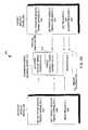
- FIG. 1illustrates an embodiment of a block diagram of an electronic design implemented in physical hardware.
- Shared communications bus 112connects sub-systems 102 , 104 , 106 , 108 , and 110 .
- Sub-systemsare typically functional blocks including an interface module for interfacing to a shared bus.
- Sub-systemsmay themselves include one or more functional blocks and may include an integrated or physically separate interface module.
- the sub-systems connected by communications bus 112are separate integrated circuit chips.
- the sub-systems connected by communications bus 112are IP cores on a SoC.
- the communicationsthemselves may be communicated over a shared bus 112 , communicated point to point, or a combination of both.
- This example electronic design systemmay be modeled.
- This example electronic design systemmay have timing information associated with transfers between the Sub-systems that are determined during simulation tests.
- the annotated timingcan be used in a chip model, which is made up of sub models of various types.
- the timing annotated channel modelcan be used to model the communications between one Intellectual Property (IP) block model and another IP block model, between one IP block model and a communications model such as a bus or interconnect, and between on communications model and another communication model.
- IPIntellectual Property
- Sub-system 104may be an application specific integrated circuit (ASIC), which is an integrated circuit designed to perform a particular function.
- Sub-system 106is a dynamic random access memory (DRAM).
- Sub-system 108is an erasable, programmable, read only memory (EPROM).
- Sub-system 110can be a field programmable gate array (FPGA).
- Sub-system 102can be a fully custom integrated circuit designed specifically to operate in system 100 .
- Other embodimentsmay contain additional sub-systems of the same types as shown, or other types not shown. Other embodiments may also include fewer sub-systems than the sub-systems shown in system 100 .
- Integrated circuit 102includes sub-systems 102 A, 102 B, 102 C, 102 D and 102 E.
- ASIC 104includes functional blocks 104 A, 104 B and 104 C.
- FPGA 110includes functional blocks 110 A and 110 B.
- a functional blockis a particular block of logic that performs a particular function, such as memory storage area, on an integrated circuit, etc.
- System 100is an example of a system that may consist of one or more integrated circuits or functional IP cores on a single chip.
- Shared communications bus 112such as a system on a chip interconnect, provides a shared communications bus between sub-systems of system 100 .
- Shared communications bus 114provides a shared communications bus between sub-systems or functional blocks on a single integrated circuit. Some of the functional blocks shown are connected to interface modules through which they send and receive signals to and from shared communications bus 112 or shared communications bus 114 .
- Interconnect 115is a local point-to-point interconnect for connecting interface modules to functional blocks.
- Interface modules 120 - 127are connected to various functional blocks as shown.
- interface modules 120 , 122 , 123 and 124are physically separated from their connected functional block (A, B, C, E and F, respectively).
- Interface modules 121 , and 125 - 128are essentially part of their respective functional blocks or sub-systems. Some functional blocks, such as 102 D, do not require a dedicated interface module. The arrangement of sub-systems, functional blocks and interface modules is flexible and is determined by the system designer.
- a typical targetis a memory device.
- a typical initiatoris a central processing unit (CPU). However, any block may be a target or an initiator for a given transaction.
- a typical bridgemight be shared communications buses 112 and 114 .
- Functional blocksall communicate with one another via shared communications bus 112 or shared communications bus 114 and the protocol of one embodiment. Initiator and target functional blocks may communicate to a shared communications bus through interface modules.
- An initiator functional blockmay communicate with a shared communications bus through an initiator interface module and a target functional block may communicate with a shared communications bus through a target interface module.
- An initiator interface moduleissues and receives read and write requests to and from functional blocks other than the one with which it is associated.
- an initiator interface moduleis typically connected to a CPU, a digital signal processing (DSP) core, or a direct memory access (DMA) engine.
- DSPdigital signal processing
- DMAdirect memory access
- interconnect shown in FIG. 1illustrates a bus based interconnect.
- the interconnectmay be implemented in many ways such as switched or routed networks.
- a computing system with a processor componentexecutes instructions to simulate an initiator module, such as sub-system 102 A, that generates a first set of timing variables.
- a target modulesuch as sub-system 102 D, generates a second set of timing variables.
- a channel modulesuch as communications bus 114 , transports transactions containing burst information for a plurality of individual transfers between the initiator module and the target module.
- the channel modulemay be modeled as an executable behavioral model and have a timing variable function to store timing variables and derive timing information associated with each individual transfer within a burst transaction during a simulation.
- the initiator modulecan be modeled to represent functional block 110 A
- the target modulecan be modeled to represent functional block 104 A
- the channel modulecan be modeled to represent communications bus 112 .
- the channel modulemay contain a processing module to calculate when each transfer in the burst information started on the channel and the latency for each transfer crossing the channel based on the timing variables available from the channel module.
- the channel modulecan be represented by the communications bus 112 in addition to one or more functional blocks for storing timing variables.
- the channel modulemay also be a point to point connection between an IP blocks such as connections 115 in FIG. 1 .
- the annotated timing variablesmay be used to closely estimate the timing of individual transfers between models of IP blocks even if the transfers were sent together in a burst at once.
- the annotated timingcan be used whether the models on each end are electronic components, communications comments, or a mixture of the two.
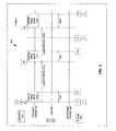
- FIG. 2Aillustrates an embodiment of a block diagram of an apparatus that provides time annotated transaction modeling.
- the apparatusincludes an initiator module model 202 , a target module model 220 , and a communications channel model 210 .
- the initiator module model 202 , target module model 220 , and communications channel model 210are each modeled as executable behavioral models.
- the executable behavioral modelcan be a transaction level model written in software language such as SystemC. Data and commands may be sent between modules using function calls.
- FIG. 2Billustrates an embodiment of a block diagram of a request transaction, having a timing field and fields associated with a burst transaction.
- the transaction 250includes a command field 260 , a data field 270 , a burst length field 274 , an address field 280 , and a timing field 290 .
- the command field 260may include the type of burst transaction, such as a write or read burst transaction, a burst pattern such as incrementing, streaming, etc, as well as the thread ID for the transaction.
- the data field 270may include one or more data words to be written to the target module model 220 or read from the target module model 220 .
- the burst length field 274may include the length of the instruction 250 .
- the address field 280may include the various addresses, such as the source and destination address of the data words to be written to the target module model 220 or read from the target module model 220 .
- the timing field 290may include timing variables and derived timing information based on the timing variables.
- the transaction 250 sent by the initiator module model 202may include timing variables generated by the initiator module model 202 .
- FIG. 2Cillustrates an embodiment of a block diagram of a response transaction, having a timing field and fields associated with a burst transaction.
- the response transaction 295includes a status field 296 , a data field 297 , a burst length field 298 , and a timing field 299 .
- the status field 296may include the status of the response, such as whether an error occurred, if the corresponding request was successful, etc., as well as a thread ID for the response.
- the data field 297may include one or more data words read from the target module model 220 .
- the burst length field 298may include the length of the response 295 .
- the timing field 299may include timing variables and derived timing information based on the timing variables.
- the transaction 295 sent by the target module model 220may include timing variables generated by the target module model 220 .
- the target module model 220sends a transaction 295 to the communications channel model 210 .
- the transaction 295may include timing variables generated by the target module model 220 .
- the communications channel model 210may examine the type of burst request generated by the initiator module model 202 and the modeled behavioral characteristics of the target module model 220 .
- the behavioral modelsmay send instructions with data fields for the target address, the initiator address, the type of burst transaction, the timing variables associated with that behavioral model, etc.
- the communications channel model 210 between the initiator module model 202 and target module model 220has a timing variable function 212 to store timing variables and derive timing information associated with each individual transfer within a burst transaction during a simulation.
- the timing variable function 212 of the communications channel model 210includes initiator module timing variables 214 and target module timing variables 216 .
- the initiator module model 202sends a function call, such as a set initiator module timing variables ( ) 204 , to the communications channel model 210 which stores the initiator module timing variables:
- the target module model 220sends a function call, such as a set target module model timing variables ( ) 224 , to the communications channel model 210 which stores the target module timing variables.
- the communications channel model 210can then derive timing information associated with each individual transfer within the burst transaction during a simulation based on timing variables received from the initiator module model 202 and the target module model 220 .
- the target module model 220may write its timing variables to the timing field of the transaction 295 .
- the initiator module model 202may write its timing variables to the timing field of the transaction 250 .
- the timing annotated TL2 channel modelhas timing information, overhead timing fields ( 290 and 299 ), stored in each transaction.
- timing informationis sent separately from the burst transaction.
- the timing information for the next (and each subsequent) transactionis set by direct function calls to the channel model. This setting of timing information by direct function calls may be easier to use in the case where the timing information does not change with every new transaction. This reduces the overhead involved, making the channel easier to use and also increases simulation performance.
- the target module model 220can access timing variables associated with the initiator module model 202 by sending a function call, such as a get initiator module model timing variables ( ) 222 , to the communications channel model 210 .
- the initiator module model 202can send a function call, such as a get target module model timing variables ( ) 206 , to the communications channel model 210 to access timing variables associated with the target module model 220 .
- the initiator module model 202 and target module model 220can both access derived timing information associated with each individual transfer within the burst transaction during a simulation by sending a function call to the communications channel model 210 .
- the initiator module model 202 and target module model 220can each calculate timing points for each transfer received within the burst transaction based on timing variables stored and timing information derived in the timing variable function of the communications channel model 210 .
- the initiator module model 202calls a function, such as a send request ( ) 208 , in the communications channel model 210 through a port that is connected to the communications channel model 210 .
- the communications channel model 210takes the request and triggers an event, request start event 230 .
- the request start event 230starts a process in the target module model 220 which then sends the function call, get request ( ) 226 , to the communications channel model 210 .
- the target module model 220may send the function call, accept request ( ) 228 to the communications channel model 210 .
- the communications channel model 210then triggers an event, request end event 240 , that the initiator module model 202 recognizes as signaling the end of the request.
- the request sent from initiator module model 202 to communications channel model 210can be accessed by the target module model 220 via a register 218 or other storage device within the communications channel model 210 .
- the channel modelmay also contain state variables stored in a hardware storage device such as a register 218 , or a memory.
- the apparatus 200illustrates a time annotated transaction model that sends both burst and timing information to the communications channel model 210 .
- a transaction modelcommunication between modules is modeled using function calls.
- a transaction modelis functionally accurate and may be cycle timing accurate or approximate.
- the communications channel model 210can be a time annotated OCP TL2 channel.
- An OCP burst transactionincludes the transporting of burst information across the OCP TL2 channel. Burst information includes request, data, and response transfers.
- a time annotated OCP TL2 burst transactionincludes the transporting of burst and the setting of the timing information associated with each individual transfer within a burst transaction. As discussed, the OCP burst transaction may not contain a timing information field 290 or timing information field 299 . Instead, the initiator module model 202 and the target module model 220 using separate function calls to the channel model set the timing information.
- the initiator module model 202can be a master module model and the target module model 220 can be a slave module model.
- the initiator module model 202can set the initiator timing variables for the burst transaction by calling a function in the channel model.
- the timing variablescan be used to derive timing points for each individual transfer of the burst.
- the target module model 220can set its timing variable fields in the channel model after it receives the burst transaction. These timing variables can be used to derive timing points for each individual transfer of the burst.
- the initiator module model 202supplies timing variables in one function call associated with a number of requests and responses. The same timing variables may then be used repeatedly for all following burst requests.
- the target module model 220also supplies timing variables in one function call associated with a number of requests and responses. The function calls between the initiator module model 202 and the target module model 220 simulate a communications protocol of the communications channel.
- the initiator module model 202 and target module model 220can each calculate timing points for each transfer received within a burst transaction based on timing variables stored and timing information derived in the timing variable function 212 of the communications channel model 210 . This can lead to high cycle timing accuracy that had merely been achievable with the much slower TL1 channel while still keeping the large performance gain from sending whole bursts at once.
- the time annotated transaction modelmay generate fast simulation times for burst transaction simulations with highly accurate timing information for each transfer in the burst transaction.
- the target module model 220sends two or more responses in a single function call.
- the initiator module model 202sends two or more requests in a single function call.
- Burst transactionssend a plurality of transfers as a group instead of one transfer at a time.
- Timing variables and derived timing information associated with all transfers in a burst transactionmay be stored.
- the derived timing informationsuch as time annotations that each transfer in the time annotated burst transaction is, for example, 10 nanoseconds apart, and may be stored in the communications channel model 210 .
- Overall, accurate timing informationis generated for each transfer that makes up the high speed time annotated burst transaction.
- the time annotated transaction modelmay also incorporate this timing point technique into other transaction level models as well.
- Each burst transactionmay have a thread ID associated with it such as in the command field ( 260 ) or the status field ( 296 ) of the transaction.
- Each burst transactionmay have timing variables, which are set to match the transaction and the thread ID associated with the transaction. Timing variable values may be different for each different transaction. Timing variables may be different for transactions with different thread IDs.
- the software used to facilitate the protocol and algorithms associated with the time annotated transaction modelingcan be embodied onto a machine-readable medium.
- a machine-readable mediumincludes any mechanism that provides (e.g., stores and/or transports) information in a form readable by a machine (e.g., a computer).
- a machine-readable mediumincludes read only memory (ROM); random access memory (RAM); magnetic disk storage media; optical storage media; flash memory devices; DVD's, EPROMs, EEPROMs, FLASH, magnetic or optical cards, or any type of media suitable for storing electronic instructions.
- the information representing the apparatuses and/or methods stored on the machine-readable mediummay be used in the process of creating the apparatuses and/or methods described herein.
- the information representing the apparatuses and/or methodsmay be contained in an Instance, soft instructions in an IP generator, or similar machine-readable medium storing this information.
- a machine-readable storage mediumhaving instructions stored thereon, which when executed by a machine, can cause the machine to generate an apparatus.
- the apparatusmay at least include an initiator module, a target module a communications channel.
- the initiator modulecan be modeled as an executable behavioral model.
- the target modulecan be modeled as an executable behavioral model.
- the communications channelis configured to transport burst information between the initiator module and the target module.
- the communications channelcan be modeled as an executable behavioral model and has timing variable functions to store timing variables and derive timing information associated with each individual transfer within a burst transaction during a simulation.
- the machine readable storage medium storing these instructionsmay perform the time annotated transaction level modeling of the apparatus containing the initiator module, the target module, and the communications channel.
- a computing systemmay at least include a processor component, a machine readable storage medium, an initiator module, a target module and a channel module.
- the processor componentcooperates with the machine readable storage medium.
- the processor componentexecutes instructions to simulate: the initiator module that generates a first set of timing variables; the target module that generates a second set of timing variables; and the channel module for transporting transactions that include burst information for a plurality of transfers between the initiator module and the target module.
- the channel moduleis configured to store the first and second set of timing variables.
- a processing modulecalculates when each transfer in the burst information started on the channel and a latency for each transfer crossing the channel module based on the first and second set of timing variables.
- a method to provide time annotated transaction level modelingincludes simulating the transporting of burst information including a plurality of transfers between the initiator module model 202 and the target module model 220 via a channel. The method further includes maintaining a first set of timing variables associated with the initiator module model 202 and maintaining a second set of timing variables associated with the target module model 220 .
- the methodmay further include simulating the communications channel module model 210 for transporting burst information across the channel, and storing the first and second set of timing variables; and calculating when each transfer in the burst information started on the channel and the latency for each transfer crossing the channel based on the first and second set of timing variables.
- the methodmay further include simulating a channel call sent from the initiator module model 202 to the communications channel module model 210 for transporting the first set of timing variables across the channel; and simulating a channel call sent from the target module model 220 to the communications channel module model 210 for transporting the second set of timing variables across the channel.
- timing diagramsillustrate various implementations of time annotated transaction modeling.
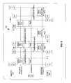
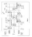
- FIG. 3illustrates an embodiment of a timing diagram for a time annotated OCP TL2 channel model with a multiple request multiple data (MRMD) posted write burst transaction with data handshake.
- the time annotated OCP TL2 channel model 300(channel 300 ) transports a burst transaction between a master module model 340 (master 340 ) and a slave module model 350 (slave 350 ).
- Each modelis an executable behavioral model.
- the executable behavioral modelcan be a transaction level model written in the SystemC language.
- the channel 300achieves a fast channel speed due to using the entire OCP burst transaction as the granularity of the model.
- the channel 300stores timing variables and derives timing information that can be used to accurately estimate the timing of the individual OCP transfers that underlie each OCP burst transaction while maintaining the efficiency of sending an entire burst as a single command.
- the stored timing variablescan include a first and second set of timing variables corresponding to the master 340 and slave 350 , respectively.
- a core modelsuch as master 340 or slave 350
- receives an OCP burst transactionthat core model can use the timing variables and derived timing information to calculate the starting and ending times of each OCP transfer that makes up the burst.
- the master 340can set the following timing variables: request data latency (RqDL), response accept latency (RpAL), request send interval (RqSndI) and data send interval (DSndI).
- the slave 350can set the following timing variables: request accept latency (RqAL), write data accept latency (DAL), and response send interval (RpSndI).
- the channel 300derives timing information based on the timing variables set by the master 340 and slave 350 .
- the derived timing informationincludes an estimated average write data interval (avgWDI), an estimated average read request interval (avgRRqI), an estimated average read data interval (avgRDI) and an estimated average write response interval (avgWRpI). Additional derived timing information includes the start time of each individual request, the start time of each individual data handshake transfer, and the total duration of the burst.
- the channel 300can be un-clocked with the timing determined by the master 340 and the slave 350 , which send function calls to the channel 300 .
- the channel 300is active when the master 340 or slave 350 has called one of its functions.
- activities for a request phase 310 , a data handshake phase (DHS) 320 , and a response phase 330 within a burst transactionare represented horizontally with simulation time increasing from left to right.
- the channel 300transports burst information such as requests on the request phase 310 , data on the DHS 320 , and responses on the response phase 330 between the master 340 and slave 350 .
- Each dashed vertical lineindicates a timing point, actual or estimated, that occurs within a burst transaction.
- a timing pointusually represents either the beginning or end of an OCP phase activity inside a burst transaction.
- the master 340 and the slave 350use the timing points to improve timing accuracy.
- the alphanumeric order among letters shown inside dashed boxes attached to the same timing point lineindicates which box occurs first.
- the number inside a dashed box, if any,indicates the transfer count.
- Latency between two interesting timing pointsis shown by a horizontal, double arrow line segment tagged with a fixed latency or a latency estimation function.
- Dashed box Arepresents the last transfer timing point where a slave can provide backpressure information to the channel 300 to prevent a request.
- Dashed box Bis the starting point of a write or read request.
- Dashed boxes B1, B2, and B3are the starting points of write data blocks in FIG. 3 .
- Dashed boxes C1, C2, and C3are the ending points of write data blocks in FIG. 3 .
- Each triangle in FIG. 3represents a function call that may need to be issued by the master 340 or slave 350 to the channel 300 .
- Triangle 1is the last time that the slave 350 can set the slave timing variables on the channel 300 for the next burst transaction.
- the slave 350can modify the slave's timing variables at triangle 1′ if mid burst backpressure is allowed. In this case, DAL was changed to DAL′.
- Triangle 2is the start time of the TL2 burst request on the channel 300 .
- Triangle 3is the end of the burst transaction.
- the times when these function calls are made to the channel 300are associated with actual simulation times given by the operation of the simulation.
- the other timing pointsare then estimated using both the actual timing points from the function calls and the timing variables passed to the channel 300 .
- time Bis the last time for the master 340 to set the master's timing variables on the channel for the upcoming burst transaction.
- the master 340calls a function to send the write burst over the channel 300 .
- the master 340sends all of the information for the write burst at this time, including the command field, a data array field, a burst length field, an address field, and other write burst transaction information.
- the burst transactionends at timing point C3 with write data 326 being received by the slave 350 .
- This timing point C3is calculated from timing variables set by the master 340 and the slave 350 as well as by the burst length of the write transaction function call from the master 340 at triangle 2.
- the slave 350accepts the burst request at triangle 3 but does not send an acknowledgement response to the master 340 in this burst transaction, which is a posted write burst.
- the start time of the first data block, write data 322can be determined from the start of burst transaction, time B, and from the request data latency (RqDL) timing variable of the master 340 .
- RqDLis the interval in clock cycles between the time when the master 340 places the request on the channel 300 and the time that the master 340 places the corresponding data block on the channel 300 .
- DSndRis defined to be the data arrival rate at which the master 340 sends data down the channel 300 if the slave were to instantly accept all data.
- the data send interval (DSndI)is 1/DSndR.
- DSndIis the interval between data blocks if the master 340 were connected to a fast slave 350 . If the master 340 can send data over the channel 300 every single clock cycle, then the DSndI would be 1. If the master 340 can merely send data every other clock cycle, then the DSndI would be 2.
- the DAL, data accept latency,is the number of clock cycles the slave 350 will take to accept each data block, such as write data 322 .
- the maximum interval of either DSndI or DALis the limiting factor that determines the avgWDI.
- DAL′ corresponding to write data 326is a larger interval (more clock cycles) compared to DAL which corresponds to write data 322 and write data 324 .
- the slave 350can be configured to update the timing information to the channel 300 .
- slave timing informationcan be provided at timing point A′ by the slave 350 .
- Mid burst timing informationis treated as auxiliary information that is optional.
- the end time of the OCP write burstoccurs at timing point C3 when the slave 350 has accepted the burst transaction. After the slave 350 determines this timing point C3, the channel 300 is then free to start a new burst. The slave 350 should accept the OCP TL2 burst transaction even if the slave command accept or slave data accept signal is not part of the OCP channel.
- FIG. 4illustrates an embodiment of a timing diagram for a time annotated OCP TL2 channel model with a multiple request multiple data (MRMD) posted write burst transaction with no data handshake.
- the time annotated OCP TL2 channel model 400(channel 400 ) transports burst information of the burst transaction between a master module model 440 (master 440 ) and a slave module model 450 (slave 450 ).
- FIG. 4The timing diagram of FIG. 4 is similar to FIG. 3 , except in FIG. 4 , the DHS 420 is turned off. In an OCP channel without data handshake, each write request and write data block are sent together. Timing points B and B1 merge as RqDL equals zero for a channel with no data handshake.
- Write/req data 412 in FIG. 4represents the same information as the combination of write req 312 and write data 322 in FIG. 3 .
- the burst transaction requeststarts at triangle 2 with the master 440 setting the master timing variables for the upcoming transaction. If the timing variables are the same as for the previous transaction, this step is optional.
- the master 440may then call a function at triangle 2 to start the write burst request on the channel.
- the burst write transaction requestmay include a command field, a data array field, a burst length field, an address field, and other OCP transaction information.
- the burst write transactionends at timing point C3 when the slave 450 accepts the burst transaction. The slave 450 does not send a response to the master 440 in this burst transaction.
- the channel 400stores timing variables set by the master 440 and the slave 450 .
- the channel 400provides timing helper functions that may be used to calculate derived timing information commonly needed by the master 440 and the slave 450 . Approximate timing points for each OCP transfer (e.g., request, data, and response transfers) can be calculated based on the timing variables stored in the channel 400 and the derived timing information provided by the timing helper functions.
- FIG. 5illustrates an embodiment of a timing diagram for a time annotated OCP TL2 channel model with a single request multiple data (SRMD) posted write burst transaction.
- the time annotated OCP TL2 channel model 500(channel 500 ) transports burst information of the burst transaction between a master module model 540 (master 540 ) and a slave module model 550 (slave 550 ).
- FIG. 5The timing diagram of FIG. 5 is similar to FIG. 3 , except in FIG. 5 , a single write request, write req 512 , is sent from the master 540 to the channel 500 . In FIG. 3 , multiple write requests are sent each corresponding to one write data block. In FIG. 5 , a single write request corresponds to all of the write data blocks of the burst.
- the master 540sets the master timing variables for the burst before sending the burst at triangle 2.
- the burst transactionstarts at triangle 2 with the master 540 sending the write burst transaction to the channel 500 .
- the write burst requestmay include a command field, a data array field, a burst length field, an address field, and other OCP fields.
- the channel 500derives the timing information from the master and slave timing variables and from the length of the burst.
- the burst transactionends at timing point C3, triangle 3, when the slave 550 accepts the burst write request. Because this is a posted write, the slave 550 does not send an acknowledgement response to the master 540 in this burst transaction.
- the channel 500stores timing variables set by the master 540 and the slave 550 .
- the channel 500provides timing helper functions that calculate derived timing information commonly needed by the master 540 and the slave 550 . Approximate timing points for each OCP transfer (e.g., request, data, and response transfers) can be calculated based on the timing variables stored in the channel 500 and the derived timing information provided by the timing helper functions even though the entire burst transaction was sent with a single function call. Large arrays of data can be quickly written within a single burst transaction while maintaining accurate timing points.
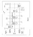
- FIG. 6illustrates an embodiment of a timing diagram for a timing annotated OCP TL2 channel model with a multiple request multiple data (MRMD) read burst transaction.
- the time annotated OCP TL2 channel model 600(channel 600 ) transports burst information of the burst transaction between a master module model 640 (master 640 ) and a slave module model 650 (slave 650 ).
- a read burstis modeled using a read burst, request-side transaction and a read burst, response-side transaction in parallel.
- a read burst's response-side transactioncan be overlapped with another read burst's request-side transaction, in terms of simulation timing.
- a read bursthas similar timing points as previously described for a write burst with a few exceptions.
- a read bursthas no request-side data block delivery.
- a read request burst from the master 640will cause a corresponding read response burst with response data from the slave 650 .
- a read bursthas new timing points including triangles 4 and 5 as well as dashed boxes D, E, and F.
- the master 640may call a function in the channel 600 to set the master timing variables for the read transaction.
- the master timing variablesare related to how quickly the master 640 can send the read request burst and how quickly the master 640 can process and accept a response burst from the slave.
- the master 640calls a function to put the read burst request on the channel 600 .
- the slave 650accepts the read burst request.
- the slave 650may call a function to set the slave timing variables on the channel. This could be necessary if the timing variables for the response had changed since the slave 650 sent the last response burst.
- the slave 650calls a function in the channel 600 to start the response burst 630 on the channel.
- the response burstmay contain fields for the status of the response, an array of the response data, the length of the response burst, and other OCP fields.
- the master 640accepts the response burst 630 .
- Dashed boxes B1, B2, and B3represent the timing points for the start of each of the read requests which make up the read burst 610 .
- Dashed boxes C1, C2, and C3are the timing points of the end of each of the read requests which make up read burst 610 .
- Dashed boxes E1, E2, and E3represent the timing points of the start of each of the read response data words which make up the response burst 630 .
- Dashed boxes F1, F2, and F3are the timing points marking the ending points of an OCP response data words which make up the read response burst 630 .
- a read burstalso has new timing variables and derived timing information including request send rate (RqSndR), request accept latency (RqAL), and average read request interval (avgRRqI).
- RqSndRrequest send rate
- RqALrequest accept latency
- avgRRqIaverage read request interval
- the request send interval(RqSndI) is 1/RqSndR.
- RqSndIis the interval between data requests if the master 640 were connected to a fast slave 650 which could instantly accept all requests. If the master 640 can send requests over the channel 600 every single clock cycle, then the RqSndI would be 1. If the master 640 can merely send requests merely every other clock cycle, then the RqSndI would be 2.
- the RqAL, data accept intervalis the number of clock cycles the slave 650 will take to accept each request. The maximum interval of either RqSndI or RqAL is the limiting factor that determines the avgRRqI.
- the RqALis set to 1.
- the same mechanism used by the write burstis used on the request-side of a read burst in order to provide the backpressure timing information with RqAL replacing DAL.
- Read requests and read data responsesare processed independently on different paths as illustrated in FIG. 6 .
- the master 640can send a size 3 read burst requesting three data words and the slave 650 could respond with two chopped responses of size 2 and size 1.
- the timing point E1is the time of the first response data, read resp/data 632 , sent over the OCP connection. There can be many read bursts for returning response data.
- the average time between read response data “i” and “i+1” of a read burst, the average read data interval (avgRDI),can be determined by two factors: how fast the slave 650 can send response data blocks down the channel (RpSndI) and how long the master 640 waits to accept the response data block (RpAL).
- avgRDImax( RpSndI,RpAL )
- RpSndIis the number of clock cycles between response data blocks if the master 640 were to instantly accept all responses. If the slave 650 can send a new response data block over the channel every single clock cycle, then the RpSndI would be 1. If the slave 650 can merely send a new response data block every other clock cycle, then the RpSndI would be 2.
- the RpAL, response accept latency,is the number of clock cycles the master 640 will take to accept a response.
- the maximum interval of either RpSndI or RpALis the limiting factor that determines the avgRDI.
- RpSndI′ corresponding to read resp/data 636is a shorter interval (less clock cycles) compared to RpSndI which corresponds to read resp/data 632 .
- the RpALis set to 1.
- the master 640can be configured to update timing information to the slave 650 .
- the master 640can set its response timing variables before the response is started at time D1.
- the mastermay change its timing values mid burst. In FIG. 6 such a mid burst timing variable change might be done at time D3. It may also optionally be set at other times during the burst.
- the burst transactionstarts at timing point B1 with the master 640 sending read req burst to the channel 600 .
- the read req burstmay include a command field, a burst length field, an address field, and other OCP fields.
- the slave 650sends the read resp/data burst to the channel 600 at timing point E1 in response to the read req burst sent at timing point B1.
- the Read resp/data burstmay include a response status field, a data array field, a burst length field, and other OCP response fields.
- the response burst transactionends at timing point F3 with read resp/data burst being accepted by the master 640 .
- the master 640can send a burst read request to the slave 650 via the channel 600 in a single function call, for example, triangle 2.
- the slave 650can send a burst read response data block to the master 640 via the channel 600 in a single function call, for example, triangle 4 in this burst transaction.
- the channel 600stores timing variables set by the master 640 and slave 650 .
- the channel 600provides timing helper functions that calculate derived timing information commonly needed by the master 640 and slave 650 . Approximate timing points for each OCP transfer (e.g., request, data, and response transfers) can be calculated based on the timing variables stored in the channel 600 and the derived timing information provided by the timing helper functions.
- FIG. 7illustrates an embodiment of a timing diagram for a time annotated OCP TL2 channel model with a single request multiple data (SRMD) read burst transaction.
- the time annotated OCP TL2 channel model 700(channel 700 ) transports burst information of the burst transaction between a master module model 740 (master 740 ) and a slave module model 750 (slave 750 ).
- the timing diagram of FIG. 7is similar to FIG. 6 , except in FIG. 7 , the read burst transaction is a single read request, read req 712 , sent from the master 740 to the channel 700 .
- the read burst transactionis a single read request, read req 712 , sent from the master 740 to the channel 700 .
- multiple read response data blocksare sent in response to the read request.
- the single read requesttriggers the response of multiple read response data blocks.
- the master 740may set the master timing variables in the channel 700 for the read burst transaction at or before triangle 2.
- the read burst transactionstarts at timing point B1 with the master 740 sending the read request burst transaction to the channel 700 .
- the read request burstmay include a command field, a burst length field, an address field, and additional OCP fields.
- the read request burstends when the slave 750 accepts the read request burst. In FIG. 7 for example this occurs at triangle 3.
- the slave 750can set the slave timing variables in the channel 700 for the response before it sends the burst response. In FIG. 7 , this would be any time before or at triangle 4.
- the slave 750sends the response burst transaction to the master 740 via the channel 700 in a single function call, for example, at triangle 4.
- the read burst responsemay include a response status field, a data array field, a burst length field, and other OCP fields.
- the response burst transactionends at timing point F3 when the master 740 accepts the response burst with a function call to the channel 700 at triangle 5.
- the channel 700stores timing variables set by the master 740 and slave 750 .
- the channel 700provides timing helper functions that calculate derived timing information commonly needed by the master 740 and slave 750 . Approximate timing points for each OCP transfer (e.g., request, data, and response transfers such as read req 712 , read resp/data 732 and read resp/data 734 ) can be calculated based on the timing variables stored in the channel 700 and the derived timing information provided by the timing helper functions even though the read request and read response were sent as single burst transactions. Large arrays of data can be quickly accessed and read within a single burst transaction while maintaining accurate timing information.
- OCP transfere.g., request, data, and response transfers such as read req 712 , read resp/data 732 and read resp/data 734
- FIG. 8illustrates an embodiment of a timing diagram for a time annotated OCP TL2 channel model with a multiple request multiple data (MRMD) non-posted write burst with data handshake on for a single write burst transaction.
- the time annotated OCP TL2 channel model 800(channel 800 ) transports burst information of the write burst transaction between a master module model 840 (master 840 ) and a slave module model 850 (slave 850 ).
- the timing diagram of FIG. 8is similar to FIG. 3 , except in FIG. 8 with a non-posted write burst, the slave 850 sends an acknowledgement response to the master 840 via the channel 800 . In FIG. 3 , the slave 350 does not send an acknowledgement response to the master 340 via the channel 300 .
- FIG. 8is similar to the timing points and variables in FIG. 6 , except no data blocks are delivered and the avgRDI used for the read burst in FIG. 6 is replaced by the average write response interval (avgWRpI) in FIG. 8 .
- the average time between write response “i” and “i+1” of a write burst, the average write response interval, (avgWRpI),can be determined by two factors: how fast the slave 850 can return a write response (RpSndI) and how long the master 840 waits to accept the write response (RpAL).
- avgWRpImax( RpSndI,RpAL )
- RpSndIis the number of clock cycles between write responses if the master 840 were to instantly accept all responses. If the slave 850 can send a new write response over the channel 800 every single clock cycle, then the RpSndI would be 1. If the slave 850 can merely send a new write response every other clock cycle, then the RpSndI would be 2.
- the RpAL, response accept latency,is the number of clock cycles the master 840 will take to accept a response.
- the maximum interval of either RpSndI or RpALis the limiting factor that determines the avgWRpI.
- RpSndI′ corresponding to write resp 836is a shorter interval (less clock cycles) compared to RpSndI which corresponds to write resp 832 .
- the burst transactionstarts at timing point B with the master 840 sending a write burst request transaction to the channel 800 .
- the write burst transactionmay include a command field, a data field, a burst length field, an address field, and other OCP fields.
- the master 840may set or change the master timing variables on the channel 800 by calling a function in the channel 800 .
- the write burst request transactionends at timing point C3 when the slave 850 accepts the write burst request transaction by calling at function in the channel 800 at triangle 3.
- the slave 850sends an acknowledgement burst response to the master 840 through the channel 800 by calling at function in the channel 800 at triangle 4.
- the slave 850may also set or change the slave timing variables at or before sending the response burst transaction at triangle 4.
- the response burst transactionends at timing point F3. This time when the master 840 accepts the response burst transaction with a function call to the channel 800 at timing triangle 5.
- the timing point F3is the time of the end of the last response acknowledgement transfer, write resp 836 in FIG. 8 .
- the master 840can send multiple write requests and write data blocks to the slave 850 via the channel 800 in a single function call, for example, triangle 2.
- the slave 850can send multiple write responses to the master 840 via the channel 800 in a single function call, for example, triangle 4.
- the channel 800stores timing variables set by the master 840 and slave 850 .
- the channel 800provides timing helper functions that calculate derived timing information commonly needed by the master 840 and slave 850 . Approximate timing points for each OCP transfer (e.g., request, data, and response transfers) can be calculated based on the timing variables stored in the channel 800 and the derived timing information provided by the timing helper functions.
- FIG. 9illustrates an embodiment of a timing diagram for a time annotated OCP TL2 channel model with a multiple request multiple data (MRMD) non-posted write burst transaction with no data handshake.
- the time annotated OCP TL2 channel model 900(channel 900 ) transports burst information of the burst transaction between a master module model 940 (master 940 ) and a slave module model 950 (slave 950 ).
- FIG. 9The timing diagram of FIG. 9 is similar to FIG. 8 , except in FIG. 9 , the data handshake, DHS 920 , is turned off. Each write request and write data block are sent together by the master 940 as illustrated in FIG. 9 . Timing points B and B1 merge because RqDL equals zero. Write/req data 912 in FIG. 9 represents the same information as write req 812 and write data 822 in FIG. 8 .
- the write request burst transactionstarts at timing point B1 with the master 940 sending a write request burst transaction to the channel 900 by calling a function at triangle 2.
- the write request burst transactionmay include a command field, a data field, a burst length field, an address field, and other OCP fields.
- the timing point B1marks the beginning of the first write request in the burst, write req/data 912 .
- the master 940may also call a function in the channel 900 to set the master timing variables in the channel 900 .
- the write request burst transactionends at timing point C3 when the slave 950 accepts the write burst request with a function call to the channel 900 at triangle 3.
- the timing point C3marks the end of the last write request in the burst, write req/dat 916 .
- the slave 950sends a burst response to the write request by calling a function in the channel 900 at triangle 4.
- the response burst transactionmay include a response status field, a burst length field, and other OCP fields.
- the start of the response burst transactionis timing point E1, which is the start of the first response transfer, write resp 932 .
- the slave 950may also set slave timing variables with a call to the channel 900 .
- the master 940accepts the response burst transaction with a call to the channel at triangle 5. This is timing point F3 in FIG.
- the master 940can send multiple write request and data blocks to the slave 950 via the channel 900 in a single function call, for example, triangle 2.
- the slave 950can send multiple write responses to the master 950 via the channel 900 in a single function call, for example, triangle 4.
- the channel 900stores timing variables set by the master 940 and slave 950 .
- the channel 900provides timing helper functions that calculate derived timing information commonly needed by the master 940 and slave 950 . Approximate timing points for each OCP transfer (e.g., request, data, and response transfers) can be calculated based on the timing variables stored in the channel 900 and the derived timing information provided by the timing helper functions.
- FIG. 10illustrates an embodiment of a timing diagram for a time annotated OCP TL2 channel model with a single request multiple data (MRMD) non-posted write burst transaction with data handshake.
- the time annotated OCP TL2 channel model 1000(channel 1000 ) transports burst information of the burst transaction between a master module model 1040 (master 1040 ) and a slave module model 1050 (slave 1050 ).
- the timing diagram of FIG. 10is similar to FIG. 8 , except in FIG. 10 , the master 1040 sends a single write request transfer to the slave 1050 and the master 1040 receives a single write response transfer from the slave 1050 .
- the master 840sends multiple write requests to the slave 850 and the master 840 receives multiple write responses from the slave 850 .
- the burst transactionstarts at timing point B with the master 1040 sending a write request burst transaction to the slave 1050 via the channel 1000 with a single function call at triangle 2.
- the write request burst transactionmay include a command field, a data field, a burst length field, an address field, and other OCP fields.
- the master 1040may also set or change the master timing variables in the channel 1000 by calling a function in the channel 1000 .
- the timing point Bis the start of the write request transfer, write req 1012
- the start of the first write data transfer, write data 1022is calculated from timing point B and the timing variable RqDL.
- the master 1040can send a single request and multiple write data blocks to the slave 1050 via the channel 1000 in a single function call, for example, triangle 2.
- the write request burst transactionends when the slave 1050 accepts the write request burst by calling a function in the channel 1000 at triangle 3.
- the slave 1050may set of change the slave timing variables by calling a function in the channel 1000 .
- the slave 1050sends a write response burst transaction via the channel 1000 with a single function call at triangle 4. This is timing point E in FIG. 10 .
- Timing point Eis the time of the start of the write response transfer, write resp 1032 .
- the write response burst transactionmay include a response status field, a burst length field, and other OCP fields.
- the write response burst transactionends when the master 1040 accepts the write response burst transaction via the channel 1000 with a single function call at triangle 5.
- the burst transactionends at timing point F3 with the single write response, write resp 1032 , being received by the master 1040 from the slave 1050 via the channel 1000 .
- the channel 1000stores timing variables set by the master 1040 and slave 1050 .
- the channel 1000provides timing helper functions that calculate derived timing information commonly needed by the master 1040 and slave 1050 . Approximate timing points for each OCP transfer (e.g., request, data, and response transfers) can be calculated based on the timing variables stored in the channel 1000 and the derived timing information provided by the timing helper functions.
Landscapes
- Engineering & Computer Science (AREA)
- Computer Hardware Design (AREA)
- Theoretical Computer Science (AREA)
- General Engineering & Computer Science (AREA)
- Physics & Mathematics (AREA)
- General Physics & Mathematics (AREA)
- Quality & Reliability (AREA)
- Evolutionary Computation (AREA)
- Geometry (AREA)
- Computer Networks & Wireless Communication (AREA)
- Signal Processing (AREA)
- Debugging And Monitoring (AREA)
Abstract
Description
B1=B+RqDL.
avgWDI=max(DSndI,DAL)
avgRRqI=max(RqSndI,RqAL)
avgRDI=max(RpSndI,RpAL)
avgWRpI=max(RpSndI,RpAL)
Claims (20)
Priority Applications (2)
| Application Number | Priority Date | Filing Date | Title |
|---|---|---|---|
| US11/203,554US9087036B1 (en) | 2004-08-12 | 2005-08-11 | Methods and apparatuses for time annotated transaction level modeling |
| US12/706,656US8504992B2 (en) | 2003-10-31 | 2010-02-16 | Method and apparatus for establishing a quality of service model |
Applications Claiming Priority (2)
| Application Number | Priority Date | Filing Date | Title |
|---|---|---|---|
| US60151904P | 2004-08-12 | 2004-08-12 | |
| US11/203,554US9087036B1 (en) | 2004-08-12 | 2005-08-11 | Methods and apparatuses for time annotated transaction level modeling |
Related Child Applications (1)
| Application Number | Title | Priority Date | Filing Date |
|---|---|---|---|
| US12/144,883Continuation-In-PartUS8407433B2 (en) | 2003-10-31 | 2008-06-24 | Interconnect implementing internal controls |
Publications (1)
| Publication Number | Publication Date |
|---|---|
| US9087036B1true US9087036B1 (en) | 2015-07-21 |
Family
ID=53540146
Family Applications (1)
| Application Number | Title | Priority Date | Filing Date |
|---|---|---|---|
| US11/203,554Active2028-03-05US9087036B1 (en) | 2003-10-31 | 2005-08-11 | Methods and apparatuses for time annotated transaction level modeling |
Country Status (1)
| Country | Link |
|---|---|
| US (1) | US9087036B1 (en) |
Cited By (5)
| Publication number | Priority date | Publication date | Assignee | Title |
|---|---|---|---|---|
| US20100318946A1 (en)* | 2005-10-07 | 2010-12-16 | Sonics, Inc. | Various methods and apparatuses for estimating characteristics of an electronic systems design |
| US20160171138A1 (en)* | 2014-12-12 | 2016-06-16 | Freescale Semiconductor, Inc. | Method and computer system for simulating operation of a programmable integrated circuit |
| US10521532B1 (en)* | 2018-09-07 | 2019-12-31 | Arm Limited | Segmented memory instances |
| CN112052074A (en)* | 2020-09-29 | 2020-12-08 | 上海兆芯集成电路有限公司 | Processor modeling system and processor modeling method |
| US11797409B1 (en) | 2022-09-02 | 2023-10-24 | HCL America Inc. | Method and system for managing transactions burstiness and generating signature thereof in a test environment |
Citations (145)
| Publication number | Priority date | Publication date | Assignee | Title |
|---|---|---|---|---|
| US4189767A (en) | 1978-06-05 | 1980-02-19 | Bell Telephone Laboratories, Incorporated | Accessing arrangement for interleaved modular memories |
| US4375097A (en) | 1978-06-02 | 1983-02-22 | Texas Instruments Incorporated | Transparent intelligent network for data and voice |
| US4393470A (en) | 1979-11-19 | 1983-07-12 | Compagnie Internationale Pour L'informatique Cii-Honeywell Bull (Societe Anonyme) | Method and device for the counting and management of asynchronous events emitted by peripheral devices in a data processing system |
| US4476498A (en) | 1982-02-05 | 1984-10-09 | Rca Corporation | Deviation detector for FM video recording system |
| US4688188A (en) | 1984-01-24 | 1987-08-18 | International Computers Limited | Data storage apparatus for storing groups of data with read and write request detection |
| US5107257A (en) | 1989-05-17 | 1992-04-21 | Nec Corporation | Bus relay apparatus for multi-data communication processing system |
| JPH0512011Y2 (en) | 1985-04-09 | 1993-03-26 | ||
| US5218456A (en) | 1991-07-22 | 1993-06-08 | Xerox Corporation | Disk bandwidth allocations to prioritize disk requests |
| US5265257A (en) | 1990-06-22 | 1993-11-23 | Digital Equipment Corporation | Fast arbiter having easy scaling for large numbers of requesters, large numbers of resource types with multiple instances of each type, and selectable queuing disciplines |
| US5274769A (en) | 1988-08-29 | 1993-12-28 | Fujitsu Limited | System for transferring data between blocks |
| US5287464A (en) | 1990-10-24 | 1994-02-15 | Zilog, Inc. | Semiconductor multi-device system with logic means for controlling the operational mode of a set of input/output data bus drivers |
| US5363484A (en) | 1990-11-13 | 1994-11-08 | International Business Machines Corporation | Multiple computer system with combiner/memory interconnection system employing separate direct access link for transferring information packets |
| US5379379A (en) | 1988-06-30 | 1995-01-03 | Wang Laboratories, Inc. | Memory control unit with selective execution of queued read and write requests |
| US5440752A (en) | 1991-07-08 | 1995-08-08 | Seiko Epson Corporation | Microprocessor architecture with a switch network for data transfer between cache, memory port, and IOU |
| US5469433A (en) | 1994-04-29 | 1995-11-21 | Bell Communications Research, Inc. | System for the parallel assembly of data transmissions in a broadband network |
| US5469473A (en) | 1994-04-15 | 1995-11-21 | Texas Instruments Incorporated | Transceiver circuit with transition detection |
| US5530901A (en) | 1991-11-28 | 1996-06-25 | Ricoh Company, Ltd. | Data Transmission processing system having DMA channels running cyclically to execute data transmission from host to memory and from memory to processing unit successively |
| US5546546A (en) | 1994-05-20 | 1996-08-13 | Intel Corporation | Method and apparatus for maintaining transaction ordering and arbitrating in a bus bridge |
| US5557754A (en) | 1992-06-22 | 1996-09-17 | International Business Machines Corporation | Computer system and system expansion unit |
| US5634006A (en) | 1992-08-17 | 1997-05-27 | International Business Machines Corporation | System and method for ensuring QOS in a token ring network utilizing an access regulator at each node for allocating frame size for plural transmitting applications based upon negotiated information and priority in the network |
| US5664153A (en) | 1993-04-21 | 1997-09-02 | Intel Corporation | Page open/close scheme based on high order address bit and likelihood of page access |
| US5673416A (en) | 1995-06-07 | 1997-09-30 | Seiko Epson Corporation | Memory request and control unit including a mechanism for issuing and removing requests for memory access |
| US5708659A (en) | 1993-10-20 | 1998-01-13 | Lsi Logic Corporation | Method for hashing in a packet network switching system |
| US5745913A (en) | 1996-08-05 | 1998-04-28 | Exponential Technology, Inc. | Multi-processor DRAM controller that prioritizes row-miss requests to stale banks |
| US5748629A (en) | 1995-07-19 | 1998-05-05 | Fujitsu Networks Communications, Inc. | Allocated and dynamic bandwidth management |
| US5781918A (en) | 1991-08-16 | 1998-07-14 | Cypress Semiconductor Corp. | Memory system and method for selecting a different number of data channels depending on bus size |
| US5809538A (en) | 1996-02-07 | 1998-09-15 | General Instrument Corporation | DRAM arbiter for video decoder |
| US5872773A (en) | 1996-05-17 | 1999-02-16 | Lucent Technologies Inc. | Virtual trees routing protocol for an ATM-based mobile network |
| US5917804A (en) | 1996-09-05 | 1999-06-29 | Northern Telecom Limited | Connection admission control for ATM networks handling CBR and VBR services |
| JPH11191075A (en) | 1997-08-28 | 1999-07-13 | Oki Electric Ind Co Ltd | Priority encoding and decoding for memory architecture |
| US5926649A (en) | 1996-10-23 | 1999-07-20 | Industrial Technology Research Institute | Media server for storage and retrieval of voluminous multimedia data |
| US5948089A (en) | 1997-09-05 | 1999-09-07 | Sonics, Inc. | Fully-pipelined fixed-latency communications system with a real time dynamic bandwidth allocation |
| JPH11250004A (en) | 1998-02-27 | 1999-09-17 | Nec Corp | Pci bus use right arbitration device |
| US5982780A (en) | 1995-12-28 | 1999-11-09 | Dynarc Ab | Resource management scheme and arrangement |
| US5996037A (en) | 1997-06-03 | 1999-11-30 | Lsi Logic Corporation | System and method for arbitrating multi-function access to a system bus |
| US6023720A (en) | 1998-02-09 | 2000-02-08 | Matsushita Electric Industrial Co., Ltd. | Simultaneous processing of read and write requests using optimized storage partitions for read and write request deadlines |
| WO2000029956A1 (en) | 1998-11-16 | 2000-05-25 | Infineon Technologies Ag | Methods and apparatus for prioritization of access to external devices |
| US6092137A (en) | 1997-11-26 | 2000-07-18 | Industrial Technology Research Institute | Fair data bus arbitration system which assigns adjustable priority values to competing sources |
| US6105094A (en) | 1998-01-26 | 2000-08-15 | Adaptec, Inc. | Method and apparatus for allocating exclusive shared resource requests in a computer system |
| US6104690A (en) | 1996-09-27 | 2000-08-15 | Digital Optics Corporation | Integrated optical apparatus and associated methods |
| US6119183A (en) | 1994-06-02 | 2000-09-12 | Storage Technology Corporation | Multi-port switching system and method for a computer bus |
| JP2000250853A (en) | 1999-03-02 | 2000-09-14 | Nec Corp | Bus arbitration controller |
| US6122690A (en) | 1997-06-05 | 2000-09-19 | Mentor Graphics Corporation | On-chip bus architecture that is both processor independent and scalable |
| US6141713A (en) | 1997-06-26 | 2000-10-31 | Hyundai Electronics Industries Co., Ltd. | Bus arbitrator with a hierarchical control structure |
| US6141355A (en) | 1998-11-06 | 2000-10-31 | Path 1 Network Technologies, Inc. | Time-synchronized multi-layer network switch for providing quality of service guarantees in computer networks |
| US6167445A (en) | 1998-10-26 | 2000-12-26 | Cisco Technology, Inc. | Method and apparatus for defining and implementing high-level quality of service policies in computer networks |
| US6182183B1 (en) | 1998-11-13 | 2001-01-30 | Sonics, Inc. | Communications system and method with multilevel connection identification |
| US6198724B1 (en) | 1997-10-02 | 2001-03-06 | Vertex Networks, Inc. | ATM cell scheduling method and apparatus |
| US6199131B1 (en) | 1997-12-22 | 2001-03-06 | Compaq Computer Corporation | Computer system employing optimized delayed transaction arbitration technique |
| US6212611B1 (en) | 1998-11-03 | 2001-04-03 | Intel Corporation | Method and apparatus for providing a pipelined memory controller |
| US6215797B1 (en) | 1998-08-19 | 2001-04-10 | Path 1 Technologies, Inc. | Methods and apparatus for providing quality of service guarantees in computer networks |
| US6215789B1 (en) | 1998-06-10 | 2001-04-10 | Merlot Communications | Local area network for the transmission and control of audio, video, and computer data |
| US6249144B1 (en) | 1997-10-09 | 2001-06-19 | Vantis Corporation | Methods for configuring FPGA's having variable grain components for providing time-shared access to interconnect resources |
| US6253269B1 (en) | 1998-12-22 | 2001-06-26 | 3Com Corporation | Bus arbiter system and method for managing communication buses |
| US6266718B1 (en) | 1998-10-14 | 2001-07-24 | Micron Technology, Inc. | Apparatus for controlling data transfer operations between a memory and devices having respective latencies |
| US20010026535A1 (en) | 2000-03-30 | 2001-10-04 | Kensaku Amou | Method and apparatus for packet scheduling in network |
| WO2001075620A1 (en) | 2000-04-03 | 2001-10-11 | Advanced Micro Devices, Inc. | Bus bridge including a memory controller having an improved memory request arbitration mechanism |
| WO2001093477A1 (en) | 2000-05-26 | 2001-12-06 | Sonics, Inc. | Communication system and method for different quality of service guarantees for different data flows |
| US6335932B2 (en) | 1998-07-08 | 2002-01-01 | Broadcom Corporation | High performance self balancing low cost network switching architecture based on distributed hierarchical shared memory |
| US6363445B1 (en) | 1998-10-15 | 2002-03-26 | Micron Technology, Inc. | Method of bus arbitration using requesting device bandwidth and priority ranking |
| US20020038397A1 (en) | 1999-12-29 | 2002-03-28 | Gurbir Singh | Quad pumped bus architecture and protocol |
| US6393500B1 (en) | 1999-08-12 | 2002-05-21 | Mips Technologies, Inc. | Burst-configurable data bus |
| US20020083256A1 (en) | 2000-08-31 | 2002-06-27 | Pannell Roger D. | System and method for increasing the count of outstanding split transactions |
| US6430156B1 (en) | 1997-12-31 | 2002-08-06 | Hyundai Electronics Inds Co Ltd. | Traffic control method for providing predictive guaranteed service |
| US20020129210A1 (en) | 2000-12-27 | 2002-09-12 | International Business Machines Corporation | Multiprocessor system snoop scheduling mechanism for limited bandwidth snoopers that uses dynamic hardware/software controls |
| US20020129173A1 (en) | 2001-03-09 | 2002-09-12 | Wolf-Dietrich Weber | Communications system and method with non-blocking shared interface |
| US20020138687A1 (en) | 2001-01-16 | 2002-09-26 | Liuxi Yang | Spin-wheel SDRAM access scheduler for high performance microprocessors |
| US6466825B1 (en) | 1998-09-29 | 2002-10-15 | Conexant Systems, Inc. | Method and apparatus for address transfers, system serialization, and centralized cache and transaction control, in a symetric multiprocessor system |
| US20020152297A1 (en) | 2000-05-23 | 2002-10-17 | Isabelle Lebourg | Quality of service control, particularly for telecommunication |
| US20020174227A1 (en) | 2000-03-03 | 2002-11-21 | Hartsell Neal D. | Systems and methods for prioritization in information management environments |
| US6487621B1 (en) | 1999-08-17 | 2002-11-26 | Compaq Information Technologies Group, L.P. | Architecture, system and method for ensuring an ordered transaction on at least one of a plurality of multi-processor buses that experience a hit-to-modified snoop cycle |
| US6499090B1 (en) | 1999-12-28 | 2002-12-24 | Intel Corporation | Prioritized bus request scheduling mechanism for processing devices |
| US20030004699A1 (en) | 2001-06-04 | 2003-01-02 | Choi Charles Y. | Method and apparatus for evaluating an integrated circuit model |
| US6510497B1 (en) | 1998-12-09 | 2003-01-21 | Advanced Micro Devices, Inc. | Method and system for page-state sensitive memory control and access in data processing systems |
| US20030023794A1 (en) | 2001-07-26 | 2003-01-30 | Venkitakrishnan Padmanabha I. | Cache coherent split transaction memory bus architecture and protocol for a multi processor chip device |
| USRE37980E1 (en) | 1996-12-31 | 2003-02-04 | Compaq Computer Corporation | Bus-to-bus bridge in computer system, with fast burst memory range |
| US6526462B1 (en) | 1999-11-19 | 2003-02-25 | Hammam Elabd | Programmable multi-tasking memory management system |
| US6530007B2 (en) | 1998-07-13 | 2003-03-04 | Compaq Information Technologies Group, L.P. | Method and apparatus for supporting heterogeneous memory in computer systems |
| US20030074519A1 (en) | 2001-10-12 | 2003-04-17 | Wolf-Dietrich Weber | Method and apparatus for scheduling of requests to dynamic random access memory device |
| US20030074520A1 (en) | 2001-10-12 | 2003-04-17 | Wolf-Dietrich Weber | Method and apparatus for scheduling requests using ordered stages of scheduling criteria |
| WO2003034242A1 (en) | 2001-10-12 | 2003-04-24 | Sonics, Inc. | Method and apparatus for scheduling a resource to meet quality-of-service restrictions |
| US20030079080A1 (en) | 2000-02-28 | 2003-04-24 | Sun Microsystems, Inc. | Disk scheduling system with bounded request reordering |
| US20030088721A1 (en) | 2001-11-05 | 2003-05-08 | Sharma Debendra Das | Method and system for controlling flow of ordered, pipelined transactions between intercommunicating electronic devices |
| US6628609B2 (en) | 1998-04-30 | 2003-09-30 | Nortel Networks Limited | Method and apparatus for simple IP-layer bandwidth allocation using ingress control of egress bandwidth |
| US6636482B2 (en) | 2001-03-08 | 2003-10-21 | Arris International, Inc. | Method and apparatus for controlling traffic loading of different service levels in a cable data system |
| US20030208614A1 (en) | 2002-05-01 | 2003-11-06 | John Wilkes | System and method for enforcing system performance guarantees |
| US6678645B1 (en)* | 1999-10-28 | 2004-01-13 | Advantest Corp. | Method and apparatus for SoC design validation |
| US20040010652A1 (en) | 2001-06-26 | 2004-01-15 | Palmchip Corporation | System-on-chip (SOC) architecture with arbitrary pipeline depth |
| US6683474B2 (en) | 2002-01-29 | 2004-01-27 | Sonic, Inc. | Method and apparatus for communication using a distributed multiplexed bus |
| US6721325B1 (en) | 1998-04-23 | 2004-04-13 | Alcatel Canada Inc. | Fair share scheduling of multiple service classes with prioritized shaping |
| US20040153928A1 (en) | 2002-12-17 | 2004-08-05 | Rohrbaugh John G. | Hierarchically-controlled automatic test pattern generation |
| US6785753B2 (en) | 2001-06-01 | 2004-08-31 | Sonics, Inc. | Method and apparatus for response modes in pipelined environment |
| US6816814B2 (en) | 2002-11-12 | 2004-11-09 | Sonics, Inc. | Method and apparatus for decomposing and verifying configurable hardware |
| US6862265B1 (en) | 2000-04-13 | 2005-03-01 | Advanced Micro Devices, Inc. | Weighted fair queuing approximation in a network switch using weighted round robin and token bucket filter |
| US6874039B2 (en) | 2000-09-08 | 2005-03-29 | Intel Corporation | Method and apparatus for distributed direct memory access for systems on chip |
| US6877076B1 (en) | 2000-09-20 | 2005-04-05 | Broadcom Corporation | Memory controller with programmable configuration |
| US6880133B2 (en) | 2002-05-15 | 2005-04-12 | Sonics, Inc. | Method and apparatus for optimizing distributed multiplexed bus interconnects |
| US6882966B2 (en)* | 1999-12-02 | 2005-04-19 | Nec Electronics Corporation | Method, and apparatus for simulating a system using an object oriented language |
| US20050086412A1 (en) | 2003-07-04 | 2005-04-21 | Cesar Douady | System and method for communicating between modules |
| US20050117589A1 (en) | 2003-08-13 | 2005-06-02 | Cesar Douady | Method and device for managing priority during the transmission of a message |
| US20050141505A1 (en) | 2003-11-13 | 2005-06-30 | Cesar Douady | System and method for transmitting a sequence of messages in an interconnection network |
| US20050144585A1 (en) | 2003-12-29 | 2005-06-30 | Jyotirmoy Daw | Method and system for hardware accelerated verification of digital circuit design and its testbench |
| US20050157717A1 (en) | 2004-01-21 | 2005-07-21 | Cesar Douady | Method and system for transmitting messages in an interconnection network |
| US20050210325A1 (en) | 2004-03-02 | 2005-09-22 | Cesar Douady | Method and device for switching between agents |
| US20050210164A1 (en) | 2004-03-11 | 2005-09-22 | Wolf-Dietrich Weber | Various methods and apparatuses for width and burst conversion |
| WO2005045727A3 (en) | 2003-10-31 | 2005-10-06 | Sonics Inc | Scheduling memory access between a plurality of processors |
| US6976106B2 (en) | 2002-11-01 | 2005-12-13 | Sonics, Inc. | Method and apparatus for speculative response arbitration to improve system latency |
| US20060047890A1 (en) | 2002-11-20 | 2006-03-02 | Van De Waerdt Jan-Willem | Sdram address mapping optimized for two-dimensional access |
| US7050958B1 (en) | 2000-06-02 | 2006-05-23 | Arm Limited | Method and apparatus for accelerating hardware simulation |
| US7062423B1 (en)* | 2001-08-22 | 2006-06-13 | Marvell International Ltd. | Method and apparatus for testing a system on a chip (SOC) integrated circuit comprising a hard disk controller and read channel |
| US20060218315A1 (en) | 2005-03-25 | 2006-09-28 | Matsushita Electric Industrial Co., Ltd. | Memory access control circuit |
| US7116131B1 (en) | 2004-09-15 | 2006-10-03 | Xilinx, Inc. | High performance programmable logic devices utilizing dynamic circuitry |
| US20060225015A1 (en) | 2005-03-31 | 2006-10-05 | Kamil Synek | Various methods and apparatuses for flexible hierarchy grouping |
| US7120765B2 (en) | 2002-10-30 | 2006-10-10 | Intel Corporation | Memory transaction ordering |
| JP2006277404A (en) | 2005-03-29 | 2006-10-12 | Nec Corp | Multiprocessor system and memory access method |
| US20060242525A1 (en) | 2005-03-31 | 2006-10-26 | Hollander Yoav Z | Method and apparatus for functionally verifying a physical device under test |
| US7149829B2 (en) | 2003-04-18 | 2006-12-12 | Sonics, Inc. | Various methods and apparatuses for arbitration among blocks of functionality |
| US7155554B2 (en) | 2004-11-02 | 2006-12-26 | Sonics, Inc. | Methods and apparatuses for generating a single request for block transactions over a communication fabric |
| US20070038791A1 (en) | 2005-08-11 | 2007-02-15 | P.A. Semi, Inc. | Non-blocking address switch with shallow per agent queues |
| US7194561B2 (en) | 2001-10-12 | 2007-03-20 | Sonics, Inc. | Method and apparatus for scheduling requests to a resource using a configurable threshold |
| US7194658B2 (en) | 2003-07-24 | 2007-03-20 | Sonics, Inc. | Various methods and apparatuses for interfacing of a protocol monitor to protocol checkers and functional checkers |
| US7194566B2 (en) | 2002-05-03 | 2007-03-20 | Sonics, Inc. | Communication system and method with configurable posting points |
| US20070083830A1 (en) | 2005-10-07 | 2007-04-12 | Stephen Hamilton | Various methods and apparatuses for an executable parameterized timing model |
| US20070110052A1 (en) | 2005-11-16 | 2007-05-17 | Sophana Kok | System and method for the static routing of data packet streams in an interconnect network |
| US7254603B2 (en) | 2002-05-03 | 2007-08-07 | Sonics, Inc. | On-chip inter-network performance optimization using configurable performance parameters |
| US7266786B2 (en) | 2002-11-05 | 2007-09-04 | Sonics, Inc. | Method and apparatus for configurable address mapping and protection architecture and hardware for on-chip systems |
| US7277975B2 (en) | 2004-11-02 | 2007-10-02 | Sonics, Inc. | Methods and apparatuses for decoupling a request from one or more solicited responses |
| US7296105B2 (en) | 2003-10-03 | 2007-11-13 | Sonics, Inc. | Method and apparatus for configuring an interconnect to implement arbitration |
| US7302691B2 (en) | 2002-05-10 | 2007-11-27 | Sonics, Incorporated | Scalable low bandwidth multicast handling in mixed core systems |
| US7325221B1 (en) | 2000-08-08 | 2008-01-29 | Sonics, Incorporated | Logic system with configurable interface |
| US20080028090A1 (en) | 2006-07-26 | 2008-01-31 | Sophana Kok | System for managing messages transmitted in an on-chip interconnect network |
| US7356633B2 (en) | 2002-05-03 | 2008-04-08 | Sonics, Inc. | Composing on-chip interconnects with configurable interfaces |
| US20080086577A1 (en) | 2006-10-04 | 2008-04-10 | Mediatek Inc. | Digital Television System, Memory Controller, and Method for Data Access |
| US20080235421A1 (en) | 2007-03-22 | 2008-09-25 | Siva Shankar Jayaratnam | Technique and apparatus to optimize inter-port memory transaction sequencing on a multi-ported memory controller unit |
| US20080320268A1 (en) | 2007-06-25 | 2008-12-25 | Sonics, Inc. | Interconnect implementing internal controls |
| US7543093B2 (en) | 2004-08-30 | 2009-06-02 | Shanghai Magima Digital Information Co., Ltd. | Method and system for stream burst data transfer |
| US7552292B2 (en) | 2004-10-29 | 2009-06-23 | Via Technologies, Inc. | Method of memory space configuration |
| US7587535B2 (en) | 2006-07-31 | 2009-09-08 | Panasonic Corporation | Data transfer control device including endian conversion circuit with data realignment |
| US7590815B1 (en) | 2002-08-30 | 2009-09-15 | Nvidia Corporation | Method and apparatus for partial memory power shutoff |
| US20090235020A1 (en) | 2007-06-25 | 2009-09-17 | Sonics, Inc. | Various methods and apparatus for address tiling |
| US7598726B1 (en) | 2005-09-12 | 2009-10-06 | Virage Logic Corporation | Methods and apparatuses for test methodology of input-output circuits |
| US20100042759A1 (en) | 2007-06-25 | 2010-02-18 | Sonics, Inc. | Various methods and apparatus for address tiling and channel interleaving throughout the integrated system |
| US20100211935A1 (en) | 2003-10-31 | 2010-08-19 | Sonics, Inc. | Method and apparatus for establishing a quality of service model |
| US7852343B2 (en) | 2004-04-15 | 2010-12-14 | Panasonic Corporation | Burst memory access method to rectangular area |
| US7899953B2 (en) | 2007-04-20 | 2011-03-01 | Nuflare Technology, Inc. | Data transfer system |
- 2005
- 2005-08-11USUS11/203,554patent/US9087036B1/enactiveActive
Patent Citations (166)
| Publication number | Priority date | Publication date | Assignee | Title |
|---|---|---|---|---|
| US4375097A (en) | 1978-06-02 | 1983-02-22 | Texas Instruments Incorporated | Transparent intelligent network for data and voice |
| US4189767A (en) | 1978-06-05 | 1980-02-19 | Bell Telephone Laboratories, Incorporated | Accessing arrangement for interleaved modular memories |
| US4393470A (en) | 1979-11-19 | 1983-07-12 | Compagnie Internationale Pour L'informatique Cii-Honeywell Bull (Societe Anonyme) | Method and device for the counting and management of asynchronous events emitted by peripheral devices in a data processing system |
| US4476498A (en) | 1982-02-05 | 1984-10-09 | Rca Corporation | Deviation detector for FM video recording system |
| US4688188A (en) | 1984-01-24 | 1987-08-18 | International Computers Limited | Data storage apparatus for storing groups of data with read and write request detection |
| JPH0512011Y2 (en) | 1985-04-09 | 1993-03-26 | ||
| US5379379A (en) | 1988-06-30 | 1995-01-03 | Wang Laboratories, Inc. | Memory control unit with selective execution of queued read and write requests |
| US5274769A (en) | 1988-08-29 | 1993-12-28 | Fujitsu Limited | System for transferring data between blocks |
| US5107257A (en) | 1989-05-17 | 1992-04-21 | Nec Corporation | Bus relay apparatus for multi-data communication processing system |
| US5265257A (en) | 1990-06-22 | 1993-11-23 | Digital Equipment Corporation | Fast arbiter having easy scaling for large numbers of requesters, large numbers of resource types with multiple instances of each type, and selectable queuing disciplines |
| US5287464A (en) | 1990-10-24 | 1994-02-15 | Zilog, Inc. | Semiconductor multi-device system with logic means for controlling the operational mode of a set of input/output data bus drivers |
| US5363484A (en) | 1990-11-13 | 1994-11-08 | International Business Machines Corporation | Multiple computer system with combiner/memory interconnection system employing separate direct access link for transferring information packets |
| US5440752A (en) | 1991-07-08 | 1995-08-08 | Seiko Epson Corporation | Microprocessor architecture with a switch network for data transfer between cache, memory port, and IOU |
| US5218456A (en) | 1991-07-22 | 1993-06-08 | Xerox Corporation | Disk bandwidth allocations to prioritize disk requests |
| US5781918A (en) | 1991-08-16 | 1998-07-14 | Cypress Semiconductor Corp. | Memory system and method for selecting a different number of data channels depending on bus size |
| US5530901A (en) | 1991-11-28 | 1996-06-25 | Ricoh Company, Ltd. | Data Transmission processing system having DMA channels running cyclically to execute data transmission from host to memory and from memory to processing unit successively |
| US5557754A (en) | 1992-06-22 | 1996-09-17 | International Business Machines Corporation | Computer system and system expansion unit |
| US5634006A (en) | 1992-08-17 | 1997-05-27 | International Business Machines Corporation | System and method for ensuring QOS in a token ring network utilizing an access regulator at each node for allocating frame size for plural transmitting applications based upon negotiated information and priority in the network |
| US5664153A (en) | 1993-04-21 | 1997-09-02 | Intel Corporation | Page open/close scheme based on high order address bit and likelihood of page access |
| US5708659A (en) | 1993-10-20 | 1998-01-13 | Lsi Logic Corporation | Method for hashing in a packet network switching system |
| US5469473A (en) | 1994-04-15 | 1995-11-21 | Texas Instruments Incorporated | Transceiver circuit with transition detection |
| US5469433A (en) | 1994-04-29 | 1995-11-21 | Bell Communications Research, Inc. | System for the parallel assembly of data transmissions in a broadband network |
| US5546546A (en) | 1994-05-20 | 1996-08-13 | Intel Corporation | Method and apparatus for maintaining transaction ordering and arbitrating in a bus bridge |
| US6119183A (en) | 1994-06-02 | 2000-09-12 | Storage Technology Corporation | Multi-port switching system and method for a computer bus |
| US5673416A (en) | 1995-06-07 | 1997-09-30 | Seiko Epson Corporation | Memory request and control unit including a mechanism for issuing and removing requests for memory access |
| US5748629A (en) | 1995-07-19 | 1998-05-05 | Fujitsu Networks Communications, Inc. | Allocated and dynamic bandwidth management |
| US5982780A (en) | 1995-12-28 | 1999-11-09 | Dynarc Ab | Resource management scheme and arrangement |
| US5809538A (en) | 1996-02-07 | 1998-09-15 | General Instrument Corporation | DRAM arbiter for video decoder |
| US5872773A (en) | 1996-05-17 | 1999-02-16 | Lucent Technologies Inc. | Virtual trees routing protocol for an ATM-based mobile network |
| US5745913A (en) | 1996-08-05 | 1998-04-28 | Exponential Technology, Inc. | Multi-processor DRAM controller that prioritizes row-miss requests to stale banks |
| US5917804A (en) | 1996-09-05 | 1999-06-29 | Northern Telecom Limited | Connection admission control for ATM networks handling CBR and VBR services |
| US6104690A (en) | 1996-09-27 | 2000-08-15 | Digital Optics Corporation | Integrated optical apparatus and associated methods |
| US5926649A (en) | 1996-10-23 | 1999-07-20 | Industrial Technology Research Institute | Media server for storage and retrieval of voluminous multimedia data |
| USRE37980E1 (en) | 1996-12-31 | 2003-02-04 | Compaq Computer Corporation | Bus-to-bus bridge in computer system, with fast burst memory range |
| US5996037A (en) | 1997-06-03 | 1999-11-30 | Lsi Logic Corporation | System and method for arbitrating multi-function access to a system bus |
| US6122690A (en) | 1997-06-05 | 2000-09-19 | Mentor Graphics Corporation | On-chip bus architecture that is both processor independent and scalable |
| US6141713A (en) | 1997-06-26 | 2000-10-31 | Hyundai Electronics Industries Co., Ltd. | Bus arbitrator with a hierarchical control structure |
| JPH11191075A (en) | 1997-08-28 | 1999-07-13 | Oki Electric Ind Co Ltd | Priority encoding and decoding for memory architecture |
| US5948089A (en) | 1997-09-05 | 1999-09-07 | Sonics, Inc. | Fully-pipelined fixed-latency communications system with a real time dynamic bandwidth allocation |
| US6198724B1 (en) | 1997-10-02 | 2001-03-06 | Vertex Networks, Inc. | ATM cell scheduling method and apparatus |
| US6249144B1 (en) | 1997-10-09 | 2001-06-19 | Vantis Corporation | Methods for configuring FPGA's having variable grain components for providing time-shared access to interconnect resources |
| US6092137A (en) | 1997-11-26 | 2000-07-18 | Industrial Technology Research Institute | Fair data bus arbitration system which assigns adjustable priority values to competing sources |
| US6199131B1 (en) | 1997-12-22 | 2001-03-06 | Compaq Computer Corporation | Computer system employing optimized delayed transaction arbitration technique |
| US6430156B1 (en) | 1997-12-31 | 2002-08-06 | Hyundai Electronics Inds Co Ltd. | Traffic control method for providing predictive guaranteed service |
| US6105094A (en) | 1998-01-26 | 2000-08-15 | Adaptec, Inc. | Method and apparatus for allocating exclusive shared resource requests in a computer system |
| US6023720A (en) | 1998-02-09 | 2000-02-08 | Matsushita Electric Industrial Co., Ltd. | Simultaneous processing of read and write requests using optimized storage partitions for read and write request deadlines |
| JPH11250004A (en) | 1998-02-27 | 1999-09-17 | Nec Corp | Pci bus use right arbitration device |
| US6721325B1 (en) | 1998-04-23 | 2004-04-13 | Alcatel Canada Inc. | Fair share scheduling of multiple service classes with prioritized shaping |
| US6628609B2 (en) | 1998-04-30 | 2003-09-30 | Nortel Networks Limited | Method and apparatus for simple IP-layer bandwidth allocation using ingress control of egress bandwidth |
| US6215789B1 (en) | 1998-06-10 | 2001-04-10 | Merlot Communications | Local area network for the transmission and control of audio, video, and computer data |
| US6335932B2 (en) | 1998-07-08 | 2002-01-01 | Broadcom Corporation | High performance self balancing low cost network switching architecture based on distributed hierarchical shared memory |
| US6530007B2 (en) | 1998-07-13 | 2003-03-04 | Compaq Information Technologies Group, L.P. | Method and apparatus for supporting heterogeneous memory in computer systems |
| US6215797B1 (en) | 1998-08-19 | 2001-04-10 | Path 1 Technologies, Inc. | Methods and apparatus for providing quality of service guarantees in computer networks |
| US6466825B1 (en) | 1998-09-29 | 2002-10-15 | Conexant Systems, Inc. | Method and apparatus for address transfers, system serialization, and centralized cache and transaction control, in a symetric multiprocessor system |
| US6266718B1 (en) | 1998-10-14 | 2001-07-24 | Micron Technology, Inc. | Apparatus for controlling data transfer operations between a memory and devices having respective latencies |
| US6363445B1 (en) | 1998-10-15 | 2002-03-26 | Micron Technology, Inc. | Method of bus arbitration using requesting device bandwidth and priority ranking |
| US6167445A (en) | 1998-10-26 | 2000-12-26 | Cisco Technology, Inc. | Method and apparatus for defining and implementing high-level quality of service policies in computer networks |
| US6212611B1 (en) | 1998-11-03 | 2001-04-03 | Intel Corporation | Method and apparatus for providing a pipelined memory controller |
| US6141355A (en) | 1998-11-06 | 2000-10-31 | Path 1 Network Technologies, Inc. | Time-synchronized multi-layer network switch for providing quality of service guarantees in computer networks |
| US20040177186A1 (en) | 1998-11-13 | 2004-09-09 | Wingard Drew Eric | Communications system and method with multilevel connection identification |
| US6182183B1 (en) | 1998-11-13 | 2001-01-30 | Sonics, Inc. | Communications system and method with multilevel connection identification |
| US7120712B2 (en) | 1998-11-13 | 2006-10-10 | Sonics, Inc. | Communications system and method with multilevel connection identification |
| US6725313B1 (en) | 1998-11-13 | 2004-04-20 | Sonics, Inc. | Communications system and method with multilevel connection identification |
| US20070094429A1 (en) | 1998-11-13 | 2007-04-26 | Wingard Drew E | Communications system and method with multilevel connection identification |
| WO2000029956A1 (en) | 1998-11-16 | 2000-05-25 | Infineon Technologies Ag | Methods and apparatus for prioritization of access to external devices |
| US6510497B1 (en) | 1998-12-09 | 2003-01-21 | Advanced Micro Devices, Inc. | Method and system for page-state sensitive memory control and access in data processing systems |
| US6253269B1 (en) | 1998-12-22 | 2001-06-26 | 3Com Corporation | Bus arbiter system and method for managing communication buses |
| JP2000250853A (en) | 1999-03-02 | 2000-09-14 | Nec Corp | Bus arbitration controller |
| US6393500B1 (en) | 1999-08-12 | 2002-05-21 | Mips Technologies, Inc. | Burst-configurable data bus |
| US6487621B1 (en) | 1999-08-17 | 2002-11-26 | Compaq Information Technologies Group, L.P. | Architecture, system and method for ensuring an ordered transaction on at least one of a plurality of multi-processor buses that experience a hit-to-modified snoop cycle |
| US6678645B1 (en)* | 1999-10-28 | 2004-01-13 | Advantest Corp. | Method and apparatus for SoC design validation |
| US6526462B1 (en) | 1999-11-19 | 2003-02-25 | Hammam Elabd | Programmable multi-tasking memory management system |
| US6882966B2 (en)* | 1999-12-02 | 2005-04-19 | Nec Electronics Corporation | Method, and apparatus for simulating a system using an object oriented language |
| US6499090B1 (en) | 1999-12-28 | 2002-12-24 | Intel Corporation | Prioritized bus request scheduling mechanism for processing devices |
| US20020038397A1 (en) | 1999-12-29 | 2002-03-28 | Gurbir Singh | Quad pumped bus architecture and protocol |
| US20030079080A1 (en) | 2000-02-28 | 2003-04-24 | Sun Microsystems, Inc. | Disk scheduling system with bounded request reordering |
| US20020174227A1 (en) | 2000-03-03 | 2002-11-21 | Hartsell Neal D. | Systems and methods for prioritization in information management environments |
| US20010026535A1 (en) | 2000-03-30 | 2001-10-04 | Kensaku Amou | Method and apparatus for packet scheduling in network |
| WO2001075620A1 (en) | 2000-04-03 | 2001-10-11 | Advanced Micro Devices, Inc. | Bus bridge including a memory controller having an improved memory request arbitration mechanism |
| US6862265B1 (en) | 2000-04-13 | 2005-03-01 | Advanced Micro Devices, Inc. | Weighted fair queuing approximation in a network switch using weighted round robin and token bucket filter |
| US20020152297A1 (en) | 2000-05-23 | 2002-10-17 | Isabelle Lebourg | Quality of service control, particularly for telecommunication |
| US6330225B1 (en) | 2000-05-26 | 2001-12-11 | Sonics, Inc. | Communication system and method for different quality of service guarantees for different data flows |
| WO2001093477A1 (en) | 2000-05-26 | 2001-12-06 | Sonics, Inc. | Communication system and method for different quality of service guarantees for different data flows |
| US7050958B1 (en) | 2000-06-02 | 2006-05-23 | Arm Limited | Method and apparatus for accelerating hardware simulation |
| US7325221B1 (en) | 2000-08-08 | 2008-01-29 | Sonics, Incorporated | Logic system with configurable interface |
| US20020083256A1 (en) | 2000-08-31 | 2002-06-27 | Pannell Roger D. | System and method for increasing the count of outstanding split transactions |
| US6874039B2 (en) | 2000-09-08 | 2005-03-29 | Intel Corporation | Method and apparatus for distributed direct memory access for systems on chip |
| US6877076B1 (en) | 2000-09-20 | 2005-04-05 | Broadcom Corporation | Memory controller with programmable configuration |
| US20020129210A1 (en) | 2000-12-27 | 2002-09-12 | International Business Machines Corporation | Multiprocessor system snoop scheduling mechanism for limited bandwidth snoopers that uses dynamic hardware/software controls |
| US20020138687A1 (en) | 2001-01-16 | 2002-09-26 | Liuxi Yang | Spin-wheel SDRAM access scheduler for high performance microprocessors |
| US6636482B2 (en) | 2001-03-08 | 2003-10-21 | Arris International, Inc. | Method and apparatus for controlling traffic loading of different service levels in a cable data system |
| US20020129173A1 (en) | 2001-03-09 | 2002-09-12 | Wolf-Dietrich Weber | Communications system and method with non-blocking shared interface |
| US6785753B2 (en) | 2001-06-01 | 2004-08-31 | Sonics, Inc. | Method and apparatus for response modes in pipelined environment |
| US20030004699A1 (en) | 2001-06-04 | 2003-01-02 | Choi Charles Y. | Method and apparatus for evaluating an integrated circuit model |
| US20040010652A1 (en) | 2001-06-26 | 2004-01-15 | Palmchip Corporation | System-on-chip (SOC) architecture with arbitrary pipeline depth |
| US20030023794A1 (en) | 2001-07-26 | 2003-01-30 | Venkitakrishnan Padmanabha I. | Cache coherent split transaction memory bus architecture and protocol for a multi processor chip device |
| US7062423B1 (en)* | 2001-08-22 | 2006-06-13 | Marvell International Ltd. | Method and apparatus for testing a system on a chip (SOC) integrated circuit comprising a hard disk controller and read channel |
| WO2003034242A1 (en) | 2001-10-12 | 2003-04-24 | Sonics, Inc. | Method and apparatus for scheduling a resource to meet quality-of-service restrictions |
| US6804757B2 (en) | 2001-10-12 | 2004-10-12 | Sonics, Inc. | Method and apparatus for scheduling requests using ordered stages of scheduling criteria |
| US6804738B2 (en) | 2001-10-12 | 2004-10-12 | Sonics, Inc. | Method and apparatus for scheduling a resource to meet quality-of-service restrictions |
| US20030074519A1 (en) | 2001-10-12 | 2003-04-17 | Wolf-Dietrich Weber | Method and apparatus for scheduling of requests to dynamic random access memory device |
| US20030074520A1 (en) | 2001-10-12 | 2003-04-17 | Wolf-Dietrich Weber | Method and apparatus for scheduling requests using ordered stages of scheduling criteria |
| US7194561B2 (en) | 2001-10-12 | 2007-03-20 | Sonics, Inc. | Method and apparatus for scheduling requests to a resource using a configurable threshold |
| US7191273B2 (en) | 2001-10-12 | 2007-03-13 | Sonics, Inc. | Method and apparatus for scheduling a resource to meet quality-of-service restrictions |
| US6578117B2 (en) | 2001-10-12 | 2003-06-10 | Sonics, Inc. | Method and apparatus for scheduling requests using ordered stages of scheduling criteria |
| US20030088721A1 (en) | 2001-11-05 | 2003-05-08 | Sharma Debendra Das | Method and system for controlling flow of ordered, pipelined transactions between intercommunicating electronic devices |
| US6683474B2 (en) | 2002-01-29 | 2004-01-27 | Sonic, Inc. | Method and apparatus for communication using a distributed multiplexed bus |
| US20030208614A1 (en) | 2002-05-01 | 2003-11-06 | John Wilkes | System and method for enforcing system performance guarantees |
| US7254603B2 (en) | 2002-05-03 | 2007-08-07 | Sonics, Inc. | On-chip inter-network performance optimization using configurable performance parameters |
| US7356633B2 (en) | 2002-05-03 | 2008-04-08 | Sonics, Inc. | Composing on-chip interconnects with configurable interfaces |
| US7194566B2 (en) | 2002-05-03 | 2007-03-20 | Sonics, Inc. | Communication system and method with configurable posting points |
| US7302691B2 (en) | 2002-05-10 | 2007-11-27 | Sonics, Incorporated | Scalable low bandwidth multicast handling in mixed core systems |
| US6880133B2 (en) | 2002-05-15 | 2005-04-12 | Sonics, Inc. | Method and apparatus for optimizing distributed multiplexed bus interconnects |
| US7590815B1 (en) | 2002-08-30 | 2009-09-15 | Nvidia Corporation | Method and apparatus for partial memory power shutoff |
| US7120765B2 (en) | 2002-10-30 | 2006-10-10 | Intel Corporation | Memory transaction ordering |
| US6976106B2 (en) | 2002-11-01 | 2005-12-13 | Sonics, Inc. | Method and apparatus for speculative response arbitration to improve system latency |
| US7266786B2 (en) | 2002-11-05 | 2007-09-04 | Sonics, Inc. | Method and apparatus for configurable address mapping and protection architecture and hardware for on-chip systems |
| US6816814B2 (en) | 2002-11-12 | 2004-11-09 | Sonics, Inc. | Method and apparatus for decomposing and verifying configurable hardware |
| US7299155B2 (en) | 2002-11-12 | 2007-11-20 | Sonics, Incorporated | Method and apparatus for decomposing and verifying configurable hardware |
| US20060047890A1 (en) | 2002-11-20 | 2006-03-02 | Van De Waerdt Jan-Willem | Sdram address mapping optimized for two-dimensional access |
| US20040153928A1 (en) | 2002-12-17 | 2004-08-05 | Rohrbaugh John G. | Hierarchically-controlled automatic test pattern generation |
| US7149829B2 (en) | 2003-04-18 | 2006-12-12 | Sonics, Inc. | Various methods and apparatuses for arbitration among blocks of functionality |
| US20050086412A1 (en) | 2003-07-04 | 2005-04-21 | Cesar Douady | System and method for communicating between modules |
| US7194658B2 (en) | 2003-07-24 | 2007-03-20 | Sonics, Inc. | Various methods and apparatuses for interfacing of a protocol monitor to protocol checkers and functional checkers |
| US20050117589A1 (en) | 2003-08-13 | 2005-06-02 | Cesar Douady | Method and device for managing priority during the transmission of a message |
| US7296105B2 (en) | 2003-10-03 | 2007-11-13 | Sonics, Inc. | Method and apparatus for configuring an interconnect to implement arbitration |
| JP5144934B2 (en) | 2003-10-31 | 2013-02-13 | ソニックス・インコーポレーテッド | Method and apparatus for establishing a quality of service model |
| EP1678620B1 (en) | 2003-10-31 | 2011-06-22 | Sonics, Inc. | Scheduling memory access between a plurality of processors |
| US20100211935A1 (en) | 2003-10-31 | 2010-08-19 | Sonics, Inc. | Method and apparatus for establishing a quality of service model |
| WO2005045727A3 (en) | 2003-10-31 | 2005-10-06 | Sonics Inc | Scheduling memory access between a plurality of processors |
| US7665069B2 (en) | 2003-10-31 | 2010-02-16 | Sonics, Inc. | Method and apparatus for establishing a quality of service model |
| KR101196048B1 (en) | 2003-10-31 | 2012-11-02 | 소닉스, 인코퍼레이티드 | Scheduling memory access between a plurality of processors |
| US20050141505A1 (en) | 2003-11-13 | 2005-06-30 | Cesar Douady | System and method for transmitting a sequence of messages in an interconnection network |
| US20050144585A1 (en) | 2003-12-29 | 2005-06-30 | Jyotirmoy Daw | Method and system for hardware accelerated verification of digital circuit design and its testbench |
| US20050157717A1 (en) | 2004-01-21 | 2005-07-21 | Cesar Douady | Method and system for transmitting messages in an interconnection network |
| US20050210325A1 (en) | 2004-03-02 | 2005-09-22 | Cesar Douady | Method and device for switching between agents |
| US7574629B2 (en) | 2004-03-02 | 2009-08-11 | Arteris | Method and device for switching between agents |
| US7543088B2 (en) | 2004-03-11 | 2009-06-02 | Sonics, Inc. | Various methods and apparatuses for width and burst conversion |
| US20050210164A1 (en) | 2004-03-11 | 2005-09-22 | Wolf-Dietrich Weber | Various methods and apparatuses for width and burst conversion |
| US7852343B2 (en) | 2004-04-15 | 2010-12-14 | Panasonic Corporation | Burst memory access method to rectangular area |
| US7543093B2 (en) | 2004-08-30 | 2009-06-02 | Shanghai Magima Digital Information Co., Ltd. | Method and system for stream burst data transfer |
| US7116131B1 (en) | 2004-09-15 | 2006-10-03 | Xilinx, Inc. | High performance programmable logic devices utilizing dynamic circuitry |
| US7552292B2 (en) | 2004-10-29 | 2009-06-23 | Via Technologies, Inc. | Method of memory space configuration |
| US7155554B2 (en) | 2004-11-02 | 2006-12-26 | Sonics, Inc. | Methods and apparatuses for generating a single request for block transactions over a communication fabric |
| US7277975B2 (en) | 2004-11-02 | 2007-10-02 | Sonics, Inc. | Methods and apparatuses for decoupling a request from one or more solicited responses |
| US20060218315A1 (en) | 2005-03-25 | 2006-09-28 | Matsushita Electric Industrial Co., Ltd. | Memory access control circuit |
| JP2006277404A (en) | 2005-03-29 | 2006-10-12 | Nec Corp | Multiprocessor system and memory access method |
| US20060225015A1 (en) | 2005-03-31 | 2006-10-05 | Kamil Synek | Various methods and apparatuses for flexible hierarchy grouping |
| US20060242525A1 (en) | 2005-03-31 | 2006-10-26 | Hollander Yoav Z | Method and apparatus for functionally verifying a physical device under test |
| US20070038791A1 (en) | 2005-08-11 | 2007-02-15 | P.A. Semi, Inc. | Non-blocking address switch with shallow per agent queues |
| US7598726B1 (en) | 2005-09-12 | 2009-10-06 | Virage Logic Corporation | Methods and apparatuses for test methodology of input-output circuits |
| US20070083830A1 (en) | 2005-10-07 | 2007-04-12 | Stephen Hamilton | Various methods and apparatuses for an executable parameterized timing model |
| US20070110052A1 (en) | 2005-11-16 | 2007-05-17 | Sophana Kok | System and method for the static routing of data packet streams in an interconnect network |
| US20080028090A1 (en) | 2006-07-26 | 2008-01-31 | Sophana Kok | System for managing messages transmitted in an on-chip interconnect network |
| US7587535B2 (en) | 2006-07-31 | 2009-09-08 | Panasonic Corporation | Data transfer control device including endian conversion circuit with data realignment |
| US20080086577A1 (en) | 2006-10-04 | 2008-04-10 | Mediatek Inc. | Digital Television System, Memory Controller, and Method for Data Access |
| US20080235421A1 (en) | 2007-03-22 | 2008-09-25 | Siva Shankar Jayaratnam | Technique and apparatus to optimize inter-port memory transaction sequencing on a multi-ported memory controller unit |
| US7899953B2 (en) | 2007-04-20 | 2011-03-01 | Nuflare Technology, Inc. | Data transfer system |
| US20090235020A1 (en) | 2007-06-25 | 2009-09-17 | Sonics, Inc. | Various methods and apparatus for address tiling |
| WO2009002998A1 (en) | 2007-06-25 | 2008-12-31 | Sonics, Inc. | An interconnect implementing internal controls |
| US20080320254A1 (en) | 2007-06-25 | 2008-12-25 | Sonics, Inc. | Various methods and apparatus to support transactions whose data address sequence within that transaction crosses an interleaved channel address boundary |
| US20100042759A1 (en) | 2007-06-25 | 2010-02-18 | Sonics, Inc. | Various methods and apparatus for address tiling and channel interleaving throughout the integrated system |
| US20080320255A1 (en) | 2007-06-25 | 2008-12-25 | Sonics, Inc. | Various methods and apparatus for configurable mapping of address regions onto one or more aggregate targets |
| US20080320476A1 (en) | 2007-06-25 | 2008-12-25 | Sonics, Inc. | Various methods and apparatus to support outstanding requests to multiple targets while maintaining transaction ordering |
| US20080320268A1 (en) | 2007-06-25 | 2008-12-25 | Sonics, Inc. | Interconnect implementing internal controls |
| US8108648B2 (en) | 2007-06-25 | 2012-01-31 | Sonics, Inc. | Various methods and apparatus for address tiling |
Non-Patent Citations (84)
| Title |
|---|
| "1st NASCUG Meeting", Meeting Presentations, http:\\www.nascug.org/nascug2004-spring.html North American SystemC Users Group, Jun. 7, 2004, pp. 2. |
| "IEEE 100: The Authoritative Dictionary of IEEE Standards Terms", 2000, IEEE, 7th Edition, IEEE Standard 100-2000, pp. 570 and 693. |
| "Intel Dual-Channel DDR Memory Architecture" White Paper Informational Brochure, Infineon Technologies North America Corporation and Kingston Technolgy Company, Inc., 14 pages, Sep. 2003. |
| "Open Core Protocol (OCP)", Wikipedia, the free encyclopedia, http://en.wikipedia.org/wiki/Open-Core-Protocol, Feb. 9, 2009, 2 pages. |
| "Open Core Protocol Specification," OCP International Partnership, Release 1.0, 2001, 2 pgs. |
| "Open Core Protocol Transaction Level 2", results of search query on Trademark Electronic Search System (TESS), United States Trademark and Patent Office, Feb. 7, 2009, 2 pages. |
| "Open Core Protocol Transaction Level 2", search query on Trademark Electronic Search System (TESS), United States Trademark and Patent Office, Feb. 7, 2009, 2 pages. |
| "Open Core Protocol", results of search query on Trademark Electronic Search System (TESS), United States Trademark and Patent Office, Feb. 7, 2009, 2 pages. |
| "Open Core Protocol", search query on Trademark Electronic Search System (TESS), United States Trademark and Patent Office, Feb. 7, 2009, 2 pages. |
| "SystemC", results of search query on Trademark Electronic Search System (TESS), United States Trademark and Patent Office, Feb. 7, 2009, 2 pages. |
| "SystemC", search query on Trademark Electronic Search System (TESS), United States Trademark and Patent Office, Feb. 7, 2009, 2 pages. |
| "SystemC", Wikipedia, the free encyclopedia, http://en.wikipedia.org/wiki/SystemC, Feb. 9, 2009, 6 pages. |
| 2nd NASCUG Meeting Agenda, Meeting Presentations, GSPx 2004, Santa Clara, CA U.S.A., Sep. 29, 2004, http://www.nascug.org/nascug2004-fall.agenda.html, North American SystemC Users Group, pp. 2. |
| Adan et al., "Queueing Models and some Fundamental Relations", Chapter 3, XP-002329104, Feb. 14, 2001, pp. 23-27 (double-sided copy). |
| Advisory Action for U.S. Appl. No. 12/706,656, mailed Nov. 15, 2012, 4 pages. U.S. Patent and Trademark Office, Alexandria, Virginia, USA. |
| Ahn, Jung Ho, et al., "The Design Space of Data-Parallel Memory Systems", IEEE, 12 pages, Nov. 2006. |
| Alan Kamas, "The SystemC OCP Models, An Overview of the SystemC Models for the Open Core Protocol", NASCUG Sep. 29, 2004, Copyright Alan Kamas 2004, www. karnas.com, pp. 30. |
| Alan Kamas. "Dot.org-Open Core Protocol: The SystemC Models" article, published in Apr./May 2004 issue of Chip Design Magazine, http://www.chipdesignmag.com/print.php?articleId=28?issueId=4, pp. 2. |
| Alexanian, H., Bolden, G., Amir, Z., "Simplifying the Behavior of System C Descriptions for Hardware/Software Covalidation," copyright 2005 [retrieved Apr. 26, 2008] Retreived from the Internet. <URL: www.ocpip.org/pressroom/schedule/speaking/papers-presentations/Summit-OCP-IP-pavillion-pres.pps>. |
| Bakr Younis et al., "Operating System for Switched Analog Mixed-Signal Circuits", The Ohio State University Department of Electrical and Computer Engineering Design Automation Research Lab (DARL), Jun. 7, 2004, pp. 12. |
| Benini et al., "Networks on Chips: A New SoC Paradigm", In IEEE 2002, Computer, vol. 35, No. 1, pp. 70-78, 9 pages. |
| Black, Co-Founder, "Eklectic Ally Electronic Systems Solutions", SystemC 2.1 Preview-DAC2004, www.EklecticAlly.com, info@EklecticAlly.com, Version 1.0, Copyright 2003, pp. 12. |
| Brian McMurtrey et al., "SystemC Enabling Embedded System Design at Sandia", Sandia National Laboratories, Apr. 14, 2004, pp. 11. |
| Casini, Phil, "Measuring the Value of Third Party Interconnects," Sonics, Inc., White Paper, 2005, 11 pages, www.sonicsinc.com. |
| Chou, Joe, "System-Level Design Using OCP Based Transaction-Level Models," presentation, Denali MemCom Taiwan 2005, OCP International Partnership, 23 pages. |
| Cottrell, Donald, Chapter 78: "Design Automation Technology Roadmap", The VLSI Handbook, Copyright 2000, 41 Pages. |
| Dally et al., "Route Packets, Not Wires: On-Chip Interconnection Networks." In Design Automation Conference, pp. 684-689, Jun. 2001, 6 pages. |
| Dally, William J., "Virtual-channel Flow Control", In Proceedings of the 17th Int. Symp. on Computer Architecture, ACM SIGARCH, May 1990, vol. 18, No. 2, pp. 60-68, 9 pages. |
| De Meer, H.; Richter, J.-P.; Puliafito, A.; Tomarchio, O., "Tunnel agents for enhanced Internet QoS," Concurrency, IEEE, vol. 6, No. 2, pp. 30-39, Apr.-Jun. 1998, URL: http//ieeexplore.ieee.org/stamp/stamp.jsp?arnumber=678787&isnumber=14923. |
| Final Office Action for U.S. Appl. No. 12/706,656, mailed Jul. 25, 2012, 37 pages. U.S. Patent and Trademark Office, Alexandria, Virginia, USA. |
| Final Preliminary Rejection (Office Action) for Korean Patent Application No. 10-20067010659 mailed Oct. 18, 2011, 6 pages. Korean Intellectual Property Office. |
| G Maruccia et al., "OCCN On-Chip-Communication-Network" From On-Chip bus to Network-on-Chip, a unique modeling framework, Advanced System Technology STMicroelectronics, Jun. 7, 2004, pp. 12. |
| Goossens et al., "Networks on Silicon: Combining Best-Effort and Guaranteed Services", In Proceeding of 2002 Design, 3 pages. |
| Gupta, Sumit and Gupta, Rajesh K., Chapter 64: "ASIC Design", The VLSI Handbook, Copyright 2000, 29 pages. |
| Hardware Verification Group, "SystemC Verification Problematic", System-on-Chip Verification , 2004, pp. 26. |
| Hardware Verification Group, "SystemC Verification Problematic", System-on-Chip Verification <http://hvg.ece.concordia.ca/Research/SoC/>, 2004, pp. 26. |
| Haverinen, "White Paper for SystemC based SoC Communication Modeling for the OCP Protocol", 2002, ICPIP, V1.0-Oct. 14, 2002. pp. 39.* |
| Ho et al., "The Future of Wires". In Proceedings of the IEEE, vol. 89, No. 4, pp. 490-504, Apr. 2001, 15 pages. |
| Hurst, Stanley L., Chapter 5: "Computer Aided Design", VLSI Custom Microelectronics: Digital, Analog, and Mixed-Signal, Copyright 1999, 95 pages. |
| International Preliminary Report on Patentability for International Patent Application No. PCT/US2008/068107, mailed Feb. 1, 2010, 7 pages. The International Bureau of WIPO, Geneva, Switzerland. |
| Jantsch, Axel, et al., "Networks on Chip", Kluwer Academic Publishers, 2003. Cover, Title Page, Contents, (4 pp.) Chapters 1-5, (pp. 3-106,) Chapters 7-8, (pp. 131-172) & Chapter 10, (pp. 193-213), 170 pages. |
| Kurose, "Open Issues and Challenges in Providing Quality of Service Guarantees in High-Speed Networks", ACM Computer Communication Review, vol. 23, No. 1, pp. 6-15, Jan. 1993, 10 pages. |
| Lahiri, K., et al., "LOTTERYBUS: A New High-Performance Communication Architecture for System-on-Chip Designs". In Proceedings of Design Automation Conference 2003, Las Vegas, Jun. 2001, pp. 15-20, 6 pages. |
| Lamport, Leslie, "How to Make a Multiprocessor Computer that Correctly Executes Multiprocess Programs", XP-009029909, IEEE Transactions on Computers, vol. C-28, No. 9, Sep. 1979, pp. 690-691 (double-sided copy). |
| Melvin, S. and Patt, Y. 2002. Handling of packet dependencies: a critical issue for highly parallel network processors. In Proceedings of the 2002 international Conference on Compilers, Architecture, and Synthesis for Embedded Systems (Grenoble, France, Oct. 8-11, 2002). Cases '02. ACM, New York, NY, 202-209. |
| Non-Final Office Action for U.S. Appl. No. 12/144,883, mailed Jun. 28, 2012, 9 pages. U.S. Patent and Trademark Office, Alexandria, Virginia, USA. |
| Non-Final Office Action for U.S. Appl. No. 12/706,656, mailed Feb. 15, 2012, 26 pages. U.S. Patent and Trademark Office, Alexandria, Virginia, USA. |
| Notice of Allowance for U.S. Appl. No. 12/144,883, mailed Nov. 21, 2012, 10 pages. U.S. Patent and Trademark Office, Alexandria, Virginia, USA. |
| Notice to File a Response (Office Action) for Korean Patent Application No. 10-20067010659 mailed Feb. 16, 2011, 3 pages. Korean Intellectual Property Office. |
| OCP (Open Core Protocol) Specification, Release 2.0, OCP International Partnership, OCP-IP Association, 210 pages, 2003. |
| Office Action for European Patent Application No. 04 796 678.3-2416 dated Dec. 14, 2007, 4 pages. European Patent Office, Munich, Germany. |
| Office Action for European Patent Application No. 04 796 678.3-2416 dated Mar. 27, 2009, 4 pages. European Patent Office, Munich, Germany. |
| Office Action for Japanese Patent Application No. 2006-538262 mailed Dec. 6, 2010, 3 pages. Japan Patent Office. |
| Office Action for Japanese Patent Application No. 2006-538262 mailed Jan. 31, 2012, 16 pages. Japan Patent Office. |
| Paul Klein et al., "Passive TLM", Intel Corporation, Paul.J.Klein@intel.com, Zafer.Kadi@intel.com, Jun. 7, 2004, pp. 16. |
| Reisslein et al., "A Framework for Guaranteeing Statistical QoS", In IEEE/ACM Transactions on Networking, vol. 10, No. 1, Feb. 2002, pp. 27-42, 16 pages. |
| Richard Ruigrok, "Hardware-Software Co-Simulation with System C", Qualcomm Incorporated, Jun. 7, 2004, pp. 17. |
| Rijpkema et al., "Trade Offs in the Design of a Router with Both Guaranteed and Best-Effort Services for Networks on Chip", In Proceedings of Design Automation and Test Conference in Europe, Mar. 2003, 6 pages. |
| Rixner, et al., "A Bandwidth-Efficient Architecture for Media Processing", Micro-31, (1998), pp. 1-11. |
| Rixner, Scott, et al., "MemoryAccess Scheduling", to appear in ISCA27 (2000), Computer Systems Laboratory, Stanford University, Stanford, CA 94305 pp. 1-11. |
| Search Report and Written Opinion for International Patent Application No. PCT/US2008/068107, mailed Oct. 8, 2008 International Searching Authority/US, Alexandria, Virginia USA. |
| Sofiene Tahar, "Assertion and Model Checking of SystemC", Hardware Verification Group, Department of Electrical and Computer Engineering, Concordia University Montreal, Quebec, Canada, First Annual North American SystemC Users Group (NASCUG) Meeting, Jun. 7, 2004, pp. 28. |
| Stiliadis et al., "Latency-Rate Servers: A General Model for Analysis of Traffic Scheduling Algorithms", In Proceedings of IEEE Infocom 96, Apr. 1996, pp. 111-119, 9 pages. |
| Stuart Swan, Senior Architect, "System C-Towards a SystemC Transaction Level Modeling Standard", Cadence Design Systems, Inc., Jun. 2004 pp. 12. |
| Summons to Oral Proceedings for European Patent Application No. 04 796 678.3-2416 dated Aug. 4, 2010, 7 pages. European Patent Office, Munich, Germany. |
| Supplementary (Extended) Search Report for European Patent Application No. 08780967 dated Dec. 21, 2010, 4 pages. European Patent Office at The Hague, Netherlands. |
| U.S. Appl. No. 11/203,554, filed Aug. 11, 2005, Chou et al. |
| U.S. Appl. No. 13/276,041, filed Oct. 18, 2011, Wingard et al. |
| United States Patent & Trademark Office, memo from Love, John J., Deputy Commissioner for Patent Examination Policy, entitled, "Clarification of Interim Guidelines for Examination of Patent Applications for Subject Matter Eligibility", Apr. 12, 2007, 2 pgs. |
| Weber, Wolf-Dietrich, et al., "A Quality-of-Search Mechanism for Interconnection Networks in System-on-Chips", Section 1530-1591/05, IEEE, 6 pages, 2005. |
| Weber, Wolf-Dietrich, et al., "Enabling Reuse via an IP Core-centric Communications Protocol: Open Core Protocol", In Proceedings of the IP 2000 System-on-Chip Conference Mar. 2000, pp. 1-5. |
| Weber, Wolf-Dietrich,"Efficient Shared DRAM Subsystems for SOCs", Sonics, Inc. Systems on the ICs, 6 pages, 2001. |
| Wielage et al., "Networks on Silicon: Blessing or Nightmare?" Keynote speech Proceedings of the Euromicro Symposium on Digital System Design, Dortmund, Germany, Sep. 2002, 5 pages. |
| Wilson Snyder, "Verilator and SystemPerl", Sun Microsystems, VeriPool, wsnyder@wsnyder.org, http://www.veripool.com, Jun. 2004, pp. 14. |
| Wingard, Drew, "A Non-Blocking Intelligent Interconnect for AMBA-Connected SoCs", Sonics, Inc., CoWare Arm Developer's Conference, 39 pages, Oct. 6, 2005. |
| Wingard, Drew, "MicroNetworks-Based Integration for SOCs." In Design Automation Conference, 2001, pp. 673-677, 5 pages. |
| Wingard, Drew, "Socket-Based Design Using Decoupled Interconnects", Interconnect-Centric Design for Advanced SOC and NOC, 30 pages, 2002. |
| Wingard, Drew, "Tiles: The Heterogeneous Processing Abstraction for MPSoc Presentation", Sonics, Smart Interconnect IP, 35 pages, Jul. 7, 2004. |
| Wingard, Drew, "Tiles-An Architectural Abstraction for Platform-Based Design," Perspective article 2, EDAVision, Jun. 2002, 3 pages, www.edavision.com. |
| Wingard, Drew, et al., "Integration Architecture for System-on-a-Chip Design", In Proc. of the 1998 Custom Integrated Circuits Conference, May 1998, pp. 85-88, 4 pages. |
| Wingard, Drew, PhD., "Integrating Semiconductor IP Using mu Networks," ASIC Design, Jul. 2000 electronic engineering, 3 pages. |
| Wingard, Drew, PhD., "Integrating Semiconductor IP Using μ Networks," ASIC Design, Jul. 2000 electronic engineering, 3 pages. |
| Wingard, Drew, Sonics SOC Integration Architecture Presentation, Systems-ON-ICS, 25 pages, Jan. 28, 1999. |
| Zhang, Hui, "Service Disciplines for Guaranteed Performance Service in Packet-Switching Networks" Proceedings of the IEEE, vol. 83, No. 10, pp. 1374-1396. Oct. 1995, DOI: 10.1109/5.469298. |
Cited By (7)
| Publication number | Priority date | Publication date | Assignee | Title |
|---|---|---|---|---|
| US20100318946A1 (en)* | 2005-10-07 | 2010-12-16 | Sonics, Inc. | Various methods and apparatuses for estimating characteristics of an electronic systems design |
| US20160171138A1 (en)* | 2014-12-12 | 2016-06-16 | Freescale Semiconductor, Inc. | Method and computer system for simulating operation of a programmable integrated circuit |
| US10521532B1 (en)* | 2018-09-07 | 2019-12-31 | Arm Limited | Segmented memory instances |
| TWI818068B (en)* | 2018-09-07 | 2023-10-11 | 英商Arm股份有限公司 | Methods and device for segmented memory instances |
| CN112052074A (en)* | 2020-09-29 | 2020-12-08 | 上海兆芯集成电路有限公司 | Processor modeling system and processor modeling method |
| CN112052074B (en)* | 2020-09-29 | 2024-05-03 | 上海兆芯集成电路股份有限公司 | Processor modeling system and processor modeling method |
| US11797409B1 (en) | 2022-09-02 | 2023-10-24 | HCL America Inc. | Method and system for managing transactions burstiness and generating signature thereof in a test environment |
Similar Documents
| Publication | Publication Date | Title |
|---|---|---|
| US10664421B1 (en) | Reordering responses in a high performance on-chip network | |
| US7778815B2 (en) | Method for the fast exploration of bus-based communication architectures at the cycle-count-accurate-at-transaction-boundaries (CCATB) abstraction | |
| US8166214B2 (en) | Shared storage for multi-threaded ordered queues in an interconnect | |
| US9311437B2 (en) | Modeling a bus for a system design incorporating one or more programmable processors | |
| US8930593B2 (en) | Method for setting parameters and determining latency in a chained device system | |
| US9600618B2 (en) | Implementing system irritator accelerator FPGA unit (AFU) residing behind a coherent attached processors interface (CAPI) unit | |
| JP5824488B2 (en) | Using completer knowledge about memory region ordering requests to modify transaction attributes | |
| JP2021514084A (en) | Optimized asynchronous training of neural networks with distributed parameter servers with lively updates | |
| US8504992B2 (en) | Method and apparatus for establishing a quality of service model | |
| CN117312215B (en) | Server system, job execution method, device, equipment and medium | |
| JP2022511581A (en) | Distributed AI training topology based on flexible cable connections | |
| JP2022510803A (en) | Memory request chain on the bus | |
| US9087036B1 (en) | Methods and apparatuses for time annotated transaction level modeling | |
| CN116089245A (en) | AXI main equipment interface-oriented pressure testing device, method and system | |
| US10409935B2 (en) | Modeling a bus for a system design incorporating one or more programmable processors | |
| CN115145638A (en) | Command distributor, command distribution method and system, chip, board card and equipment | |
| CN114021715B (en) | Deep learning training method based on Tensorflow framework | |
| US7987437B2 (en) | Structure for piggybacking multiple data tenures on a single data bus grant to achieve higher bus utilization | |
| US10803223B2 (en) | System and method for designing a chip floorplan using machine learning | |
| US10073795B1 (en) | Data compression engine for I/O processing subsystem | |
| CN115859894B (en) | Integrated circuit design method, relay module database construction method and device | |
| US20230169226A1 (en) | Method and system for interfacing a testbench to circuit simulation | |
| Danowitz | Exploring abstract interfaces in system-on-chip integration | |
| CN120295812A (en) | Bus modeling method, device, computer equipment and storage medium | |
| Raijada | Ethernet GMAC IP Verification |
Legal Events
| Date | Code | Title | Description |
|---|---|---|---|
| AS | Assignment | Owner name:SONICS, INC., CALIFORNIA Free format text:ASSIGNMENT OF ASSIGNORS INTEREST;ASSIGNORS:CHOU, CHIEN-CHUN;KAMAS, ALAN;REEL/FRAME:017071/0206 Effective date:20050812 | |
| AS | Assignment | Owner name:PARTNERS FOR GROWTH, L.P., CALIFORNIA Free format text:SECURITY AGREEMENT;ASSIGNOR:SONICS, INC.;REEL/FRAME:016886/0376 Effective date:20050526 | |
| AS | Assignment | Owner name:SONICS, INC., CALIFORNIA Free format text:RELEASE BY SECURED PARTY;ASSIGNOR:PARTNERS FOR GROWTH, L.P.;REEL/FRAME:035790/0758 Effective date:20120410 | |
| STCF | Information on status: patent grant | Free format text:PATENTED CASE | |
| MAFP | Maintenance fee payment | Free format text:PAYMENT OF MAINTENANCE FEE, 4TH YEAR, LARGE ENTITY (ORIGINAL EVENT CODE: M1551); ENTITY STATUS OF PATENT OWNER: LARGE ENTITY Year of fee payment:4 | |
| AS | Assignment | Owner name:FACEBOOK TECHNOLOGIES, LLC, CALIFORNIA Free format text:MERGER AND CHANGE OF NAME;ASSIGNORS:SONICS, INC.;FACEBOOK TECHNOLOGIES, LLC;REEL/FRAME:049442/0332 Effective date:20181227 | |
| AS | Assignment | Owner name:META PLATFORMS TECHNOLOGIES, LLC, CALIFORNIA Free format text:CHANGE OF NAME;ASSIGNOR:FACEBOOK TECHNOLOGIES, LLC;REEL/FRAME:060130/0404 Effective date:20220318 | |
| MAFP | Maintenance fee payment | Free format text:PAYMENT OF MAINTENANCE FEE, 8TH YEAR, LARGE ENTITY (ORIGINAL EVENT CODE: M1552); ENTITY STATUS OF PATENT OWNER: LARGE ENTITY Year of fee payment:8 |