US9082353B2 - Circuits for controlling display apparatus - Google Patents
Circuits for controlling display apparatusDownload PDFInfo
- Publication number
- US9082353B2 US9082353B2US12/652,477US65247710AUS9082353B2US 9082353 B2US9082353 B2US 9082353B2US 65247710 AUS65247710 AUS 65247710AUS 9082353 B2US9082353 B2US 9082353B2
- Authority
- US
- United States
- Prior art keywords
- voltage
- interconnect
- update
- shutter
- data
- Prior art date
- Legal status (The legal status is an assumption and is not a legal conclusion. Google has not performed a legal analysis and makes no representation as to the accuracy of the status listed.)
- Expired - Fee Related, expires
Links
- 238000000034methodMethods0.000claimsabstractdescription79
- 230000009977dual effectEffects0.000claimsdescription42
- 239000003990capacitorSubstances0.000claimsdescription35
- 238000011068loading methodMethods0.000claimsdescription29
- 230000008569processEffects0.000claimsdescription16
- 230000008878couplingEffects0.000claimsdescription5
- 238000010168coupling processMethods0.000claimsdescription5
- 238000005859coupling reactionMethods0.000claimsdescription5
- 239000011159matrix materialSubstances0.000abstractdescription108
- 230000033001locomotionEffects0.000abstractdescription11
- 239000000758substrateSubstances0.000description28
- 238000010586diagramMethods0.000description27
- 230000000712assemblyEffects0.000description21
- 238000000429assemblyMethods0.000description21
- 238000005286illuminationMethods0.000description12
- 230000006870functionEffects0.000description9
- 238000010348incorporationMethods0.000description9
- 239000003086colorantSubstances0.000description8
- 230000000903blocking effectEffects0.000description7
- 238000012423maintenanceMethods0.000description7
- 230000004044responseEffects0.000description7
- 230000007704transitionEffects0.000description7
- 238000004519manufacturing processMethods0.000description6
- 230000003287optical effectEffects0.000description6
- 238000013500data storageMethods0.000description5
- 239000011521glassSubstances0.000description5
- 239000003921oilSubstances0.000description5
- 230000003071parasitic effectEffects0.000description5
- 239000010409thin filmSubstances0.000description5
- 230000001052transient effectEffects0.000description5
- 230000015572biosynthetic processEffects0.000description4
- 238000006073displacement reactionMethods0.000description4
- 238000003384imaging methodMethods0.000description4
- 239000000463materialSubstances0.000description4
- XUIMIQQOPSSXEZ-UHFFFAOYSA-NSiliconChemical compound[Si]XUIMIQQOPSSXEZ-UHFFFAOYSA-N0.000description3
- 210000004556brainAnatomy0.000description3
- 239000004973liquid crystal related substanceSubstances0.000description3
- 239000004033plasticSubstances0.000description3
- 238000012163sequencing techniqueMethods0.000description3
- 229910052710siliconInorganic materials0.000description3
- 239000010703siliconSubstances0.000description3
- 239000012780transparent materialSubstances0.000description3
- 239000011358absorbing materialSubstances0.000description2
- 238000003491arrayMethods0.000description2
- 230000006399behaviorEffects0.000description2
- 230000000295complement effectEffects0.000description2
- 238000001514detection methodMethods0.000description2
- 238000005516engineering processMethods0.000description2
- 230000007613environmental effectEffects0.000description2
- 238000005530etchingMethods0.000description2
- 238000005459micromachiningMethods0.000description2
- 238000012545processingMethods0.000description2
- 238000005096rolling processMethods0.000description2
- 239000004065semiconductorSubstances0.000description2
- 238000000926separation methodMethods0.000description2
- 241001270131Agaricus moelleriSpecies0.000description1
- 230000009471actionEffects0.000description1
- 230000003213activating effectEffects0.000description1
- 230000004913activationEffects0.000description1
- 238000007792additionMethods0.000description1
- WYTGDNHDOZPMIW-RCBQFDQVSA-NalstonineNatural productsC1=CC2=C3C=CC=CC3=NC2=C2N1C[C@H]1[C@H](C)OC=C(C(=O)OC)[C@H]1C2WYTGDNHDOZPMIW-RCBQFDQVSA-N0.000description1
- 229910021417amorphous siliconInorganic materials0.000description1
- 230000005540biological transmissionEffects0.000description1
- 230000008859changeEffects0.000description1
- 238000005229chemical vapour depositionMethods0.000description1
- 230000002301combined effectEffects0.000description1
- 230000007423decreaseEffects0.000description1
- 238000013461designMethods0.000description1
- 230000005684electric fieldEffects0.000description1
- 238000000605extractionMethods0.000description1
- 238000001914filtrationMethods0.000description1
- 239000012530fluidSubstances0.000description1
- 238000010237hybrid techniqueMethods0.000description1
- 230000000415inactivating effectEffects0.000description1
- AMGQUBHHOARCQH-UHFFFAOYSA-Nindium;oxotinChemical compound[In].[Sn]=OAMGQUBHHOARCQH-UHFFFAOYSA-N0.000description1
- 230000000977initiatory effectEffects0.000description1
- 239000007924injectionSubstances0.000description1
- 238000002347injectionMethods0.000description1
- 230000001788irregularEffects0.000description1
- 230000007246mechanismEffects0.000description1
- 239000012528membraneSubstances0.000description1
- 239000002184metalSubstances0.000description1
- 238000001393microlithographyMethods0.000description1
- 238000012986modificationMethods0.000description1
- 230000004048modificationEffects0.000description1
- 230000008447perceptionEffects0.000description1
- 230000000737periodic effectEffects0.000description1
- 230000001360synchronised effectEffects0.000description1
- 230000001131transforming effectEffects0.000description1
- 230000000007visual effectEffects0.000description1
- XLYOFNOQVPJJNP-UHFFFAOYSA-NwaterSubstancesOXLYOFNOQVPJJNP-UHFFFAOYSA-N0.000description1
Images


Classifications
- G—PHYSICS
- G02—OPTICS
- G02B—OPTICAL ELEMENTS, SYSTEMS OR APPARATUS
- G02B26/00—Optical devices or arrangements for the control of light using movable or deformable optical elements
- G02B26/02—Optical devices or arrangements for the control of light using movable or deformable optical elements for controlling the intensity of light
- G02B26/04—Optical devices or arrangements for the control of light using movable or deformable optical elements for controlling the intensity of light by periodically varying the intensity of light, e.g. using choppers
- G—PHYSICS
- G09—EDUCATION; CRYPTOGRAPHY; DISPLAY; ADVERTISING; SEALS
- G09G—ARRANGEMENTS OR CIRCUITS FOR CONTROL OF INDICATING DEVICES USING STATIC MEANS TO PRESENT VARIABLE INFORMATION
- G09G3/00—Control arrangements or circuits, of interest only in connection with visual indicators other than cathode-ray tubes
- G09G3/20—Control arrangements or circuits, of interest only in connection with visual indicators other than cathode-ray tubes for presentation of an assembly of a number of characters, e.g. a page, by composing the assembly by combination of individual elements arranged in a matrix no fixed position being assigned to or needed to be assigned to the individual characters or partial characters
- G09G3/34—Control arrangements or circuits, of interest only in connection with visual indicators other than cathode-ray tubes for presentation of an assembly of a number of characters, e.g. a page, by composing the assembly by combination of individual elements arranged in a matrix no fixed position being assigned to or needed to be assigned to the individual characters or partial characters by control of light from an independent source
- G09G3/3433—Control arrangements or circuits, of interest only in connection with visual indicators other than cathode-ray tubes for presentation of an assembly of a number of characters, e.g. a page, by composing the assembly by combination of individual elements arranged in a matrix no fixed position being assigned to or needed to be assigned to the individual characters or partial characters by control of light from an independent source using light modulating elements actuated by an electric field and being other than liquid crystal devices and electrochromic devices
- G09G3/346—Control arrangements or circuits, of interest only in connection with visual indicators other than cathode-ray tubes for presentation of an assembly of a number of characters, e.g. a page, by composing the assembly by combination of individual elements arranged in a matrix no fixed position being assigned to or needed to be assigned to the individual characters or partial characters by control of light from an independent source using light modulating elements actuated by an electric field and being other than liquid crystal devices and electrochromic devices based on modulation of the reflection angle, e.g. micromirrors
- G—PHYSICS
- G02—OPTICS
- G02B—OPTICAL ELEMENTS, SYSTEMS OR APPARATUS
- G02B26/00—Optical devices or arrangements for the control of light using movable or deformable optical elements
- G02B26/08—Optical devices or arrangements for the control of light using movable or deformable optical elements for controlling the direction of light
- G02B26/0816—Optical devices or arrangements for the control of light using movable or deformable optical elements for controlling the direction of light by means of one or more reflecting elements
- G02B26/0833—Optical devices or arrangements for the control of light using movable or deformable optical elements for controlling the direction of light by means of one or more reflecting elements the reflecting element being a micromechanical device, e.g. a MEMS mirror, DMD
- G02B26/0841—Optical devices or arrangements for the control of light using movable or deformable optical elements for controlling the direction of light by means of one or more reflecting elements the reflecting element being a micromechanical device, e.g. a MEMS mirror, DMD the reflecting element being moved or deformed by electrostatic means
- G—PHYSICS
- G09—EDUCATION; CRYPTOGRAPHY; DISPLAY; ADVERTISING; SEALS
- G09G—ARRANGEMENTS OR CIRCUITS FOR CONTROL OF INDICATING DEVICES USING STATIC MEANS TO PRESENT VARIABLE INFORMATION
- G09G3/00—Control arrangements or circuits, of interest only in connection with visual indicators other than cathode-ray tubes
- G09G3/20—Control arrangements or circuits, of interest only in connection with visual indicators other than cathode-ray tubes for presentation of an assembly of a number of characters, e.g. a page, by composing the assembly by combination of individual elements arranged in a matrix no fixed position being assigned to or needed to be assigned to the individual characters or partial characters
- G09G3/2003—Display of colours
- G—PHYSICS
- G09—EDUCATION; CRYPTOGRAPHY; DISPLAY; ADVERTISING; SEALS
- G09G—ARRANGEMENTS OR CIRCUITS FOR CONTROL OF INDICATING DEVICES USING STATIC MEANS TO PRESENT VARIABLE INFORMATION
- G09G3/00—Control arrangements or circuits, of interest only in connection with visual indicators other than cathode-ray tubes
- G09G3/20—Control arrangements or circuits, of interest only in connection with visual indicators other than cathode-ray tubes for presentation of an assembly of a number of characters, e.g. a page, by composing the assembly by combination of individual elements arranged in a matrix no fixed position being assigned to or needed to be assigned to the individual characters or partial characters
- G09G3/2007—Display of intermediate tones
- G09G3/2018—Display of intermediate tones by time modulation using two or more time intervals
- G09G3/2022—Display of intermediate tones by time modulation using two or more time intervals using sub-frames
- G—PHYSICS
- G09—EDUCATION; CRYPTOGRAPHY; DISPLAY; ADVERTISING; SEALS
- G09G—ARRANGEMENTS OR CIRCUITS FOR CONTROL OF INDICATING DEVICES USING STATIC MEANS TO PRESENT VARIABLE INFORMATION
- G09G3/00—Control arrangements or circuits, of interest only in connection with visual indicators other than cathode-ray tubes
- G09G3/20—Control arrangements or circuits, of interest only in connection with visual indicators other than cathode-ray tubes for presentation of an assembly of a number of characters, e.g. a page, by composing the assembly by combination of individual elements arranged in a matrix no fixed position being assigned to or needed to be assigned to the individual characters or partial characters
- G09G3/2007—Display of intermediate tones
- G09G3/2074—Display of intermediate tones using sub-pixels
- G—PHYSICS
- G09—EDUCATION; CRYPTOGRAPHY; DISPLAY; ADVERTISING; SEALS
- G09G—ARRANGEMENTS OR CIRCUITS FOR CONTROL OF INDICATING DEVICES USING STATIC MEANS TO PRESENT VARIABLE INFORMATION
- G09G3/00—Control arrangements or circuits, of interest only in connection with visual indicators other than cathode-ray tubes
- G09G3/20—Control arrangements or circuits, of interest only in connection with visual indicators other than cathode-ray tubes for presentation of an assembly of a number of characters, e.g. a page, by composing the assembly by combination of individual elements arranged in a matrix no fixed position being assigned to or needed to be assigned to the individual characters or partial characters
- G09G3/34—Control arrangements or circuits, of interest only in connection with visual indicators other than cathode-ray tubes for presentation of an assembly of a number of characters, e.g. a page, by composing the assembly by combination of individual elements arranged in a matrix no fixed position being assigned to or needed to be assigned to the individual characters or partial characters by control of light from an independent source
- G09G3/3433—Control arrangements or circuits, of interest only in connection with visual indicators other than cathode-ray tubes for presentation of an assembly of a number of characters, e.g. a page, by composing the assembly by combination of individual elements arranged in a matrix no fixed position being assigned to or needed to be assigned to the individual characters or partial characters by control of light from an independent source using light modulating elements actuated by an electric field and being other than liquid crystal devices and electrochromic devices
- H—ELECTRICITY
- H03—ELECTRONIC CIRCUITRY
- H03K—PULSE TECHNIQUE
- H03K3/00—Circuits for generating electric pulses; Monostable, bistable or multistable circuits
- H03K3/02—Generators characterised by the type of circuit or by the means used for producing pulses
- H03K3/027—Generators characterised by the type of circuit or by the means used for producing pulses by the use of logic circuits, with internal or external positive feedback
- H03K3/037—Bistable circuits
- G—PHYSICS
- G09—EDUCATION; CRYPTOGRAPHY; DISPLAY; ADVERTISING; SEALS
- G09G—ARRANGEMENTS OR CIRCUITS FOR CONTROL OF INDICATING DEVICES USING STATIC MEANS TO PRESENT VARIABLE INFORMATION
- G09G2300/00—Aspects of the constitution of display devices
- G09G2300/04—Structural and physical details of display devices
- G09G2300/0439—Pixel structures
- G09G2300/0456—Pixel structures with a reflective area and a transmissive area combined in one pixel, such as in transflectance pixels
- G—PHYSICS
- G09—EDUCATION; CRYPTOGRAPHY; DISPLAY; ADVERTISING; SEALS
- G09G—ARRANGEMENTS OR CIRCUITS FOR CONTROL OF INDICATING DEVICES USING STATIC MEANS TO PRESENT VARIABLE INFORMATION
- G09G2300/00—Aspects of the constitution of display devices
- G09G2300/08—Active matrix structure, i.e. with use of active elements, inclusive of non-linear two terminal elements, in the pixels together with light emitting or modulating elements
- G09G2300/0809—Several active elements per pixel in active matrix panels
- G09G2300/0814—Several active elements per pixel in active matrix panels used for selection purposes, e.g. logical AND for partial update
- G—PHYSICS
- G09—EDUCATION; CRYPTOGRAPHY; DISPLAY; ADVERTISING; SEALS
- G09G—ARRANGEMENTS OR CIRCUITS FOR CONTROL OF INDICATING DEVICES USING STATIC MEANS TO PRESENT VARIABLE INFORMATION
- G09G2300/00—Aspects of the constitution of display devices
- G09G2300/08—Active matrix structure, i.e. with use of active elements, inclusive of non-linear two terminal elements, in the pixels together with light emitting or modulating elements
- G09G2300/0809—Several active elements per pixel in active matrix panels
- G09G2300/0842—Several active elements per pixel in active matrix panels forming a memory circuit, e.g. a dynamic memory with one capacitor
- G09G2300/0857—Static memory circuit, e.g. flip-flop
- G—PHYSICS
- G09—EDUCATION; CRYPTOGRAPHY; DISPLAY; ADVERTISING; SEALS
- G09G—ARRANGEMENTS OR CIRCUITS FOR CONTROL OF INDICATING DEVICES USING STATIC MEANS TO PRESENT VARIABLE INFORMATION
- G09G2310/00—Command of the display device
- G09G2310/02—Addressing, scanning or driving the display screen or processing steps related thereto
- G09G2310/0235—Field-sequential colour display
- G—PHYSICS
- G09—EDUCATION; CRYPTOGRAPHY; DISPLAY; ADVERTISING; SEALS
- G09G—ARRANGEMENTS OR CIRCUITS FOR CONTROL OF INDICATING DEVICES USING STATIC MEANS TO PRESENT VARIABLE INFORMATION
- G09G2310/00—Command of the display device
- G09G2310/02—Addressing, scanning or driving the display screen or processing steps related thereto
- G09G2310/0243—Details of the generation of driving signals
- G09G2310/0251—Precharge or discharge of pixel before applying new pixel voltage
- G—PHYSICS
- G09—EDUCATION; CRYPTOGRAPHY; DISPLAY; ADVERTISING; SEALS
- G09G—ARRANGEMENTS OR CIRCUITS FOR CONTROL OF INDICATING DEVICES USING STATIC MEANS TO PRESENT VARIABLE INFORMATION
- G09G2310/00—Command of the display device
- G09G2310/02—Addressing, scanning or driving the display screen or processing steps related thereto
- G09G2310/0262—The addressing of the pixel, in a display other than an active matrix LCD, involving the control of two or more scan electrodes or two or more data electrodes, e.g. pixel voltage dependent on signals of two data electrodes
- G—PHYSICS
- G09—EDUCATION; CRYPTOGRAPHY; DISPLAY; ADVERTISING; SEALS
- G09G—ARRANGEMENTS OR CIRCUITS FOR CONTROL OF INDICATING DEVICES USING STATIC MEANS TO PRESENT VARIABLE INFORMATION
- G09G2360/00—Aspects of the architecture of display systems
- G09G2360/14—Detecting light within display terminals, e.g. using a single or a plurality of photosensors
- G09G2360/144—Detecting light within display terminals, e.g. using a single or a plurality of photosensors the light being ambient light
- G—PHYSICS
- G09—EDUCATION; CRYPTOGRAPHY; DISPLAY; ADVERTISING; SEALS
- G09G—ARRANGEMENTS OR CIRCUITS FOR CONTROL OF INDICATING DEVICES USING STATIC MEANS TO PRESENT VARIABLE INFORMATION
- G09G3/00—Control arrangements or circuits, of interest only in connection with visual indicators other than cathode-ray tubes
- G09G3/20—Control arrangements or circuits, of interest only in connection with visual indicators other than cathode-ray tubes for presentation of an assembly of a number of characters, e.g. a page, by composing the assembly by combination of individual elements arranged in a matrix no fixed position being assigned to or needed to be assigned to the individual characters or partial characters
- G09G3/34—Control arrangements or circuits, of interest only in connection with visual indicators other than cathode-ray tubes for presentation of an assembly of a number of characters, e.g. a page, by composing the assembly by combination of individual elements arranged in a matrix no fixed position being assigned to or needed to be assigned to the individual characters or partial characters by control of light from an independent source
- G09G3/3406—Control of illumination source
- G09G3/3413—Details of control of colour illumination sources
Definitions
- the inventionrelates to the field of imaging displays, in particular, the invention relates to controller circuits and processes for controlling light modulators incorporated into imaging displays.
- Displays built from mechanical light modulatorsare an attractive alternative to displays based on liquid crystal technology.
- Mechanical light modulatorsare fast enough to display video content with good viewing angles and with a wide range of color and grey scale. Mechanical light modulators have been successful in projection display applications.
- Direct-view displays using mechanical light modulatorshave not yet demonstrated sufficiently attractive combinations of brightness and low power.
- the inventionrelates to direct-view display apparatuses including an array of pixels.
- the array of pixelsinclude, for each pixel, a MEMS-based light modulator formed on a substrate, and a first actuator and a second actuator opposing the first actuator for controlling the state of the light modulator to form an image on the display apparatus.
- the array of pixelsinclude a control matrix disposed on the substrate which includes a dual inverter latch coupling the first and second actuators and configured to maintain an opposite logical state on the first and second actuators.
- the substrateis a transparent substrate.
- the dual inverter latchincludes two cross-coupled inverters.
- the two cross-coupled invertersmay include two transistors, dual gate transistors, may be connected to a cascode circuit, or any combination thereof.
- the display apparatusincludes a data store in which the dual inverter latch is latched in the first state based, at least in part, on a data voltage stored in the data store.
- the display apparatusincludes a switch coupling the data store to the dual inverter latch for allowing the data to pass from the data store to the dual inverter latch.
- the switchis controlled by a common voltage interconnect for a plurality of rows and columns.
- the switchfunctions to electrically de-couple the data store from the dual inverter latch to prevent current from flowing between the data store and the dual inverter latch.
- the display apparatusincludes an actuation line interconnect.
- the actuation line interconnectis configured to provide a voltage to only one of the first and second actuators for actuating the light modulator to form an image.
- the actuation line interconnectprovides an intermediate voltage to latch the dual inverter latch in a first state corresponding to the data voltage.
- the inventionrelates to a method for addressing pixels in a display in which each pixel includes a MEMS based light modulator, first and second actuators, and a dual inverter latch coupling the first and second actuators for maintaining an opposite logical state on the first and second actuators.
- the methodincludes loading data into a data store coupled to the dual inverter latch, updating the latch state based at least in part on the loaded data such that a full actuation voltage is only applied to one of the first and second actuators, and actuating the MEMS based light modulator.
- actuating the MEMS-based light modulatorincludes applying voltages to the MEMS-based light modulator and to the first and second actuators in accordance with a polarity reversal process.
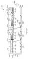
- FIG. 1Ais an isometric view of display apparatus, according to an illustrative embodiment of the invention.
- FIG. 1Bis a block diagram of the display apparatus of FIG. 1A , according to an illustrative embodiment of the invention.
- FIG. 1Cis a timing diagram for a method of displaying an image on a display using a field sequential color technique, according to an illustrative embodiment of the invention
- FIG. 1Dis a timing diagram illustrating the timing of various image formation events using a coded time division grayscale technique, according to an illustrative embodiment of the invention
- FIG. 2Ais a perspective view of an illustrative shutter-based light modulator suitable for incorporation into the MEMS-based display of FIG. 1A , according to an illustrative embodiment of the invention
- FIG. 2Bis a cross-sectional view of a rollershade-based light modulator suitable for incorporation into the MEMS-based display of FIG. 1A , according to an illustrative embodiment of the invention
- FIG. 2Cis a cross sectional view of a light-tap-based light modulator suitable for incorporation into an alternative embodiment of the MEMS-based display of FIG. 1A , according to an illustrative embodiment of the invention
- FIG. 2Dis a cross sectional view of an electrowetting-based light modulator suitable for incorporation into an alternative embodiment of the MEMS-based display of FIG. 1A , according to an illustrative embodiment of the invention
- FIG. 3Ais a schematic diagram of a control matrix suitable for controlling the light modulators incorporated into the MEMS-based display of FIG. 1A , according to an illustrative embodiment of the invention
- FIG. 3Bis a perspective view of an array of shutter-based light modulators connected to the control matrix of FIG. 3A , according to an illustrative embodiment of the invention
- FIGS. 4A and 4Bare plan views of a dual-actuated shutter assembly in the open and closed states respectively, according to an illustrative embodiment of the invention.
- FIG. 4Cis a cross sectional view of a dual actuator light tap-based light modulator suitable for incorporation into the MEMS-based display, according to an illustrative embodiment of the invention.
- FIG. 5Ais a diagram of a control matrix suitable for controlling the shutter assemblies of the display apparatus of FIG. 1A , according to an illustrative embodiment of the invention
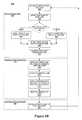
- FIG. 5Bis a flow chart of a method of addressing the pixels of the control matrix of FIG. 5A , according to an illustrative embodiment of the invention
- FIG. 6is a diagram of a control matrix suitable for controlling the shutter assemblies of the display apparatus of FIG. 1A , according to an illustrative embodiment of the invention
- FIG. 7is a diagram of a control matrix suitable for controlling the shutter assemblies of the display apparatus of FIG. 1A , according to an illustrative embodiment of the invention.
- FIG. 8is a diagram of a control matrix suitable for controlling the shutter assemblies of the display apparatus of FIG. 1A , according to an illustrative embodiment of the invention.
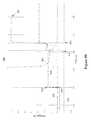
- FIG. 9Ais a chart of voltage variations vs. time during pixel operation, according to an illustrative embodiment of the invention.
- FIG. 9Bis a chart of voltage transition detail during pixel actuation, according to an illustrative embodiment of the invention.
- FIG. 10Ais a chart of the voltage increase on an actuator node during pixel operation, according to an illustrative embodiment of the invention.
- FIG. 10Bis a chart of the latch current transient of the coupled transistors during pixel operation, according to an illustrative embodiment of the invention.
- FIG. 11Ais a chart of the voltage increase on an actuator node during pixel operation, according to an illustrative embodiment of the invention.
- FIG. 11Bis a chart of the latch current transient of the coupled transistors during pixel operation, according to an illustrative embodiment of the invention.
- FIG. 1is a schematic diagram of a direct-view MEMS-based display apparatus 100 , according to an illustrative embodiment of the invention.
- the display apparatus 100includes a plurality of light modulators 102 a - 102 d (generally “light modulators 102 ”) arranged in rows and columns.
- light modulators 102 a and 102 dare in the open state, allowing light to pass.
- Light modulators 102 b and 102 care in the closed state, obstructing the passage of light.
- the display apparatus 100can be utilized to form an image 104 for a backlit display, if illuminated by a lamp or lamps 105 .
- the apparatus 100may form an image by reflection of ambient light originating from the front of the apparatus.
- the apparatus 100may form an image by reflection of light from a lamp or lamps positioned in the front of the display, i.e. by use of a frontlight.
- the light modulators 102interfere with light in an optical path by, for example, and without limitation, blocking, reflecting, absorbing, filtering, polarizing, diffracting, or otherwise altering a property or path of the light.
- each light modulator 102corresponds to a pixel 106 in the image 104 .
- the display apparatus 100may utilize a plurality of light modulators to form a pixel 106 in the image 104 .
- the display apparatus 100may include three color-specific light modulators 102 . By selectively opening one or more of the color-specific light modulators 102 corresponding to a particular pixel 106 , the display apparatus 100 can generate a color pixel 106 in the image 104 .
- the display apparatus 100includes two or more light modulators 102 per pixel 106 to provide grayscale in an image 104 .
- a “pixel”corresponds to the smallest picture element defined by the resolution of the image.
- the term “pixel”refers to the combined mechanical and electrical components utilized to modulate the light that forms a single pixel of the image.
- Display apparatus 100is a direct-view display in that it does not require imaging optics. The user sees an image by looking directly at the display apparatus 100 .
- the display apparatus 100is incorporated into a projection display.
- the displayforms an image by projecting light onto a screen or onto a wall.
- the display apparatus 100is substantially smaller than the projected image 104 .
- Direct-view displaysmay operate in either a transmissive or reflective mode.
- the light modulatorsfilter or selectively block light which originates from a lamp or lamps positioned behind the display. The light from the lamps is optionally injected into a light guide or “backlight”.
- Transmissive direct-view display embodimentsare often built onto transparent or glass substrates to facilitate a sandwich assembly arrangement where one substrate, containing the light modulators, is positioned directly on top of the backlight.
- a color-specific light modulatoris created by associating a color filter material with each modulator 102 .
- colorscan be generated, as described below, using a field sequential color method by alternating illumination of lamps with different primary colors.
- Each light modulator 102includes a shutter 108 and an aperture 109 .
- the shutter 108is positioned such that it allows light to pass through the aperture 109 towards a viewer.
- the shutter 108is positioned such that it obstructs the passage of light through the aperture 109 .
- the aperture 109is defined by an opening patterned through a reflective or light-absorbing material.
- the display apparatusalso includes a control matrix connected to the substrate and to the light modulators for controlling the movement of the shutters.
- the control matrixincludes a series of electrical interconnects (e.g., interconnects 110 , 112 , and 114 ), including at least one write-enable interconnect 110 (also referred to as a “scan-line interconnect”) per row of pixels, one data interconnect 112 for each column of pixels, and one common interconnect 114 providing a common voltage to all pixels, or at least to pixels from both multiple columns and multiples rows in the display apparatus 100 .
- V wethe write-enable interconnect 110 for a given row of pixels prepares the pixels in the row to accept new shutter movement instructions.
- the data interconnects 112communicate the new movement instructions in the form of data voltage pulses.
- the data voltage pulses applied to the data interconnects 112directly contribute to an electrostatic movement of the shutters.
- the data voltage pulsescontrol switches, e.g., transistors or other non-linear circuit elements that control the application of separate actuation voltages, which are typically higher in magnitude than the data voltages, to the light modulators 102 . The application of these actuation voltages then results in the electrostatic driven movement of the shutters 108 .
- FIG. 1Bis a block diagram 150 of the display apparatus 100 .
- the display apparatus 100includes a plurality of scan drivers 152 (also referred to as “write enabling voltage sources”) and a plurality of data drivers 154 (also referred to as “data voltage sources”).
- the scan drivers 152apply write enabling voltages to scan-line interconnects 110 .
- the data drivers 154apply data voltages to the data interconnects 112 .
- the data drivers 154are configured to provide analog data voltages to the light modulators, especially where the gray scale of the image 104 is to be derived in analog fashion.
- the light modulators 102are designed such that when a range of intermediate voltages is applied through the data interconnects 112 there results a range of intermediate open states in the shutters 108 and therefore a range of intermediate illumination states or gray scales in the image 104 .
- the data drivers 154are configured to apply only a reduced set of 2, 3, or 4 digital voltage levels to the control matrix. These voltage levels are designed to set, in digital fashion, either an open state or a closed state to each of the shutters 108 .
- the scan drivers 152 and the data drivers 154are connected to digital controller circuit 156 (also referred to as the “controller 156 ”).
- the controller 156includes an input processing module 158 , which processes an incoming image signal 157 into a digital image format appropriate to the spatial addressing and the gray scale capabilities of the display 100 .
- the pixel location and gray scale data of each imageis stored in a frame buffer 159 so that the data can be fed out as needed to the data drivers 154 .
- the datais sent to the data drivers 154 in mostly serial fashion, organized in predetermined sequences grouped by rows and by image frames.
- the data drivers 154can include series to parallel data converters, level shifting, and for some applications digital to analog voltage converters.
- the display 100 apparatusoptionally includes a set of common drivers 153 , also referred to as common voltage sources.
- the common drivers 153provide a DC common potential to all light modulators within the array of light modulators 103 , for instance by supplying voltage to a series of common interconnects 114 .
- the common drivers 153following commands from the controller 156 , issue voltage pulses or signals to the array of light modulators 103 , for instance global actuation pulses which are capable of driving and/or initiating simultaneous actuation of all light modulators in multiple rows and columns of the array 103 .
- All of the driverse.g., scan drivers 152 , data drivers 154 , and common drivers 153 ) for different display functions are time-synchronized by a timing-control module 160 in the controller 156 .
- Timing commands from the module 160coordinate the illumination of red, green and blue and white lamps ( 162 , 164 , 166 , and 167 respectively) via lamp drivers 168 , the write-enabling and sequencing of specific rows within the array of pixels 103 , the output of voltages from the data drivers 154 , and the output of voltages that provide for light modulator actuation.
- the controller 156determines the sequencing or addressing scheme by which each of the shutters 108 in the array 103 can be re-set to the illumination levels appropriate to a new image 104 . Details of suitable addressing, image formation, and gray scale techniques can be found in U.S. patent application Ser. Nos. 11/326,696 and 11/643,042, incorporated herein by reference. New images 104 can be set at periodic intervals. For instance, for video displays, the color images 104 or frames of video are refreshed at frequencies ranging from 10 to 300 Hertz.
- the setting of an image frame to the array 103is synchronized with the illumination of the lamps 162 , 164 , and 166 such that alternate image frames are illuminated with an alternating series of colors, such as red, green, and blue.
- the image frames for each respective coloris referred to as a color sub-frame.
- the field sequential color methodif the color sub-frames are alternated at frequencies in excess of 20 Hz, the human brain will average the alternating frame images into the perception of an image having a broad and continuous range of colors.
- four or more lamps with primary colorscan be employed in display apparatus 100 , employing primaries other than red, green, and blue.
- the controller 156determines the addressing sequence and/or the time intervals between image frames to produce images 104 with appropriate gray scale.
- the process of generating varying levels of grayscale by controlling the amount of time a shutter 108 is open in a particular frameis referred to as time division gray scale.
- the controller 156determines the time period or the fraction of time within each frame that a shutter 108 is allowed to remain in the open state, according to the illumination level or gray scale desired of that pixel.
- the controller 156sets a plurality of sub-frame images in multiple rows and columns of the array 103 , and the controller alters the duration over which each sub-frame image is illuminated in proportion to a gray scale value or significance value employed within a coded word for gray scale.
- the illumination times for a series of sub-frame imagescan be varied in proportion to the binary coding series 1, 2, 4, 8 . . . .
- the shutters 108 for each pixel in the array 103are then set to either the open or closed state within a sub-frame image according to the value at a corresponding position within the pixel's binary coded word for gray level.
- the controlleralters the intensity of light from the lamps 162 , 164 , and 166 in proportion to the gray scale value desired for a particular sub-frame image.
- a number of hybrid techniquesare also available for forming colors and gray scale from an array of shutters 108 .
- the time division techniques described abovecan be combined with the use of multiple shutters 108 per pixel, or the gray scale value for a particular sub-frame image can be established through a combination of both sub-frame timing and lamp intensity. Details of these and other embodiments can be found in U.S. patent application Ser. No. 11/643,042, referenced above.
- the data for an image state 104is loaded by the controller 156 to the modulator array 103 by a sequential addressing of individual rows, also referred to as scan lines.
- the scan driver 152applies a write-enable voltage to the write enable interconnect 110 for that row of the array 103 , and subsequently the data driver 154 supplies data voltages, corresponding to desired shutter states, for each column in the selected row. This process repeats until data has been loaded for all rows in the array.
- the sequence of selected rows for data loadingis linear, proceeding from top to bottom in the array.
- the sequence of selected rowsis pseudo-randomized, in order to minimize visual artifacts.
- the sequencingis organized by blocks, where, for a block, the data for only a certain fraction of the image state 104 is loaded to the array, for instance by addressing only every 5 th row of the array in sequence.
- the process for loading image data to the array 103is separated in time from the process of actuating the shutters 108 .
- the modulator array 103may include data memory elements for each pixel in the array 103 and the control matrix may include a global actuation interconnect for carrying trigger signals, from common driver 153 , to initiate simultaneous actuation of shutters 108 according to data stored in the memory elements.
- Various addressing sequencesmany of which are described in U.S. patent application Ser. No. 11/643,042, can be coordinated by means of the timing control module 160 .
- the array of pixels 103 and the control matrix that controls the pixelsmay be arranged in configurations other than rectangular rows and columns.
- the pixelscan be arranged in hexagonal arrays or curvilinear rows and columns.
- the term scan-lineshall refer to any plurality of pixels that share a write-enabling interconnect.
- the display 100is comprised of a plurality of functional blocks including the timing control module 160 , the frame buffer 159 , scan drivers 152 , data drivers 154 , and drivers 153 and 168 .
- Each blockcan be understood to represent either a distinguishable hardware circuit and/or a module of executable code.
- the functional blocksare provided as distinct chips or circuits connected together by means of circuit boards and/or cables. Alternately, many of these circuits can be fabricated along with the pixel array 103 on the same substrate of glass or plastic. In other implementations, multiple circuits, drivers, processors, and/or control functions from block diagram 150 may be integrated together within a single silicon chip, which is then bonded directly to the transparent substrate holding pixel array 103 .
- the controller 156includes a programming link 180 by which the addressing, color, and/or gray scale algorithms, which are implemented within controller 156 , can be altered according to the needs of particular applications.
- the programming link 180conveys information from environmental sensors, such as ambient light or temperature sensors, so that the controller 156 can adjust imaging modes or backlight power in correspondence with environmental conditions.
- the controller 156also comprises a power supply input 182 which provides the power needed for lamps as well as light modulator actuation.
- the drivers 152 153 , 154 , and/or 168may include or be associated with DC-DC converters for transforming an input voltage at 182 into various voltages sufficient for the actuation of shutters 108 or illumination of the lamps, such as lamps 162 , 164 , 166 , and 167 .
- the human brainin response to viewing rapidly changing images, for example, at frequencies of greater than 20 Hz, averages images together to perceive an image which is the combination of the images displayed within a corresponding period.
- This phenomenoncan be utilized to display color images while using only single light modulators for each pixel of a display, using a technique referred to in the art as field sequential color.
- field sequential color techniqueseliminates the need for color filters and multiple light modulators per pixel.
- an image frame to be displayedis divided into a number of sub-frame images, each corresponding to a particular color component (for example, red, green, or blue) of the original image frame.
- the light modulators of a displayare set into states corresponding to the color component's contribution to the image.
- the light modulatorsthen are illuminated by a lamp of the corresponding color.
- the sub-imagesare displayed in sequence at a frequency (for example, greater than 60 Hz) sufficient for the brain to perceive the series of sub-frame images as a single image.
- the data used to generate the sub-framesare often fractured in various memory components. For example, in some displays, data for a given row of display are kept in a shift-register dedicated to that row. Image data is shifted in and out of each shift register to a light modulator in a corresponding column in that row of the display according to a fixed clock cycle.
- FIG. 1Cis a timing diagram corresponding to a display process for displaying images using field sequential color, which can be implemented according to an illustrative embodiment of the invention, for example, by a MEMS direct-view display described in FIG. 1B .
- the timing diagrams included herein, including the timing diagram of FIG. 1Cconform to the following conventions.
- the top portions of the timing diagramsillustrate light modulator addressing events.
- the bottom portionsillustrate lamp illumination events.
- the addressing portionsdepict addressing events by diagonal lines spaced apart in time. Each diagonal line corresponds to a series of individual data loading events during which data is loaded into each row of an array of light modulators, one row at a time. Depending on the control matrix used to address and drive the modulators included in the display, each loading event may require a waiting period to allow the light modulators in a given row to actuate. In some implementations, all rows in the array of light modulators are addressed prior to actuation of any of the light modulators. Upon completion of loading data into the last row of the array of light modulators, all light modulators are actuated substantially simultaneously.
- Lamp illumination eventsare illustrated by pulse trains corresponding to each color of lamp included in the display. Each pulse indicates that the lamp of the corresponding color is illuminated, thereby displaying the sub-frame image loaded into the array of light modulators in the immediately preceding addressing event.
- the time at which the first addressing event in the display of a given image frame beginsis labeled on each timing diagram as AT 0 . In most of the timing diagrams, this time falls shortly after the detection of a voltage pulse vsync, which precedes the beginning of each video frame received by a display.
- the times at which each subsequent addressing event takes placeare labeled as AT 1 , AT 2 , . . . AT(n ⁇ 1), where n is the number of sub-frame images used to display the image frame.
- the diagonal linesare further labeled to indicate the data being loaded into the array of light modulators. For example, in the timing diagram of FIG.
- D 0represents the first data loaded into the array of light modulators for a frame and D(n ⁇ 1) represents the last data loaded into the array of light modulators for the frame.
- the data loaded during each addressing eventcorresponds to a bitplane.
- FIG. 1Dis a timing diagram that corresponds to a coded-time division grayscale display process in which image frames are displayed by displaying four sub-frame images for each of three color components (red, green, and blue) of the image frame.
- Each sub-frame image displayed of a given coloris displayed at the same intensity for half as long a time period as the prior sub-frame image, thereby implementing a binary weighting scheme for the sub-frame images.
- the display of an image framebegins upon the detection of a vsync pulse.
- the first sub-frame data set R 3stored beginning at memory location M 0 , is loaded into the array of light modulators 103 in an addressing event that begins at time AT 0 .
- the red lampis then illuminated at time LT 0 .
- LT 0is selected such that it occurs after each of the rows in the array of light modulators 103 has been addressed, and the light modulators included therein have actuated.
- the controller 156 of the direct-view displayboth extinguishes the red lamp and begins loading the subsequent bitplane, R 2 , into the array of light modulators 103 .
- This bitplaneis stored beginning at memory location M 1 .
- the processrepeats until all bitplanes have been displayed. For example, at time AT 4 , the controller 156 extinguishes the red lamp and begins loading the most significant green bitplane, G 3 , into the array of light modulators 103 . Similarly at time LT 6 , the controller 156 turns on the green lamp until time AT 7 , at which it time it is extinguished again.
- the time period between vsync pulses in the timing diagramis indicated by the symbol FT, indicating a frame time.
- the addressing times AT 0 , AT 1 , etc. as well as the lamp times LT 0 , LT 1 , etc.are designed to accomplish 4 sub-frame images per color within a frame time FT of 16.6 milliseconds, i.e. according to a frame rate of 60 Hz.
- the time valuescan be altered to accomplish 4 sub-frame images per color within a frame time FT of 33.3 milliseconds, i.e. according to a frame rate of 30 Hz.
- frame rates as low as 24 Hzmay be employed or frame rates in excess of 100 Hz may be employed.
- the controlleroutputs 4 sub-frame images to the array 103 of light modulators for each color to be displayed.
- the illumination of each of the 4 sub-frame imagesis weighted according to the binary series 1, 2, 4, 8.
- the display process in the timing diagram of FIG. 1Dtherefore, displays a 4-digit binary word for gray scale in each color, that is, it is capable of displaying 16 distinct gray scale levels for each color, despite the loading of only 4 sub-images per color.
- the implementation of the timing diagram of FIG. 1Dis capable of displaying more than 4000 distinct colors.
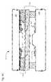
- FIG. 2Ais a perspective view of an illustrative shutter-based light modulator 200 suitable for incorporation into the MEMS-based display apparatus 100 of FIG. 1A , according to an illustrative embodiment of the invention.
- the shutter-based light modulator 200(also referred to as shutter assembly 200 ) includes a shutter 202 coupled to an actuator 204 .
- the actuator 204is formed from two separate compliant electrode beam actuators 205 (the “actuators 205 ”), as described in U.S. Pat. No. 7,271,945, filed on Sep. 18, 2007.
- the shutter 202couples on one side to the actuators 205 .
- the actuators 205move the shutter 202 transversely over a surface 203 in a plane of motion which is substantially parallel to the surface 203 .
- the opposite side of the shutter 202couples to a spring 207 which provides a restoring force opposing the forces exerted by the actuator 204 .
- Each actuator 205includes a compliant load beam 206 connecting the shutter 202 to a load anchor 208 .
- the load anchors 208along with the compliant load beams 206 serve as mechanical supports, keeping the shutter 202 suspended proximate to the surface 203 .
- the load anchors 208physically connect the compliant load beams 206 and the shutter 202 to the surface 203 and electrically connect the load beams 206 to a bias voltage, in some instances, ground.
- Each actuator 205also includes a compliant drive beam 216 positioned adjacent to each load beam 206 .
- the drive beams 216couple at one end to a drive beam anchor 218 shared between the drive beams 216 .
- the other end of each drive beam 216is free to move.
- Each drive beam 216is curved such that it is closest to the load beam 206 near the free end of the drive beam 216 and the anchored end of the load beam 206 .
- the surface 203includes one or more apertures 211 for admitting the passage of light. If the shutter assembly 200 is formed on an opaque substrate, made, for example, from silicon, then the surface 203 is a surface of the substrate, and the apertures 211 are formed by etching an array of holes through the substrate. If the shutter assembly 200 is formed on a transparent substrate, made, for example, of glass or plastic, then the surface 203 is a surface of a light blocking layer deposited on the substrate, and the apertures are formed by etching the surface 203 into an array of holes 211 .
- the apertures 211can be generally circular, elliptical, polygonal, serpentine, or irregular in shape.
- a display apparatus incorporating the light modulator 200applies an electric potential to the drive beams 216 via the drive beam anchor 218 .
- a second electric potentialmay be applied to the load beams 206 .
- the resulting potential difference between the drive beams 216 and the load beams 206pulls the free ends of the drive beams 216 towards the anchored ends of the load beams 206 , and pulls the shutter ends of the load beams 206 toward the anchored ends of the drive beams 216 , thereby driving the shutter 202 transversely towards the drive anchor 218 .
- the compliant members 206act as springs, such that when the voltage across the beams 206 and 216 is removed, the load beams 206 push the shutter 202 back into its initial position, releasing the stress stored in the load beams 206 .
- the shutter assembly 200also referred to as an elastic shutter assembly, incorporates a passive restoring force, such as a spring, for returning a shutter to its rest or relaxed position after voltages have been removed.
- a passive restoring forcesuch as a spring
- a number of elastic restore mechanisms and various electrostatic couplingscan be designed into or in conjunction with electrostatic actuators, the compliant beams illustrated in shutter assembly 200 being just one example. Other examples are described in U.S. Pat. No. 7,271,945 and U.S. patent application Ser. No. 11/326,696, incorporated herein by reference.
- a highly non-linear voltage-displacement responsecan be provided which favors an abrupt transition between “open” vs “closed” states of operation, and which, in many cases, provides a bi-stable or hysteretic operating characteristic for the shutter assembly.
- Other electrostatic actuatorscan be designed with more incremental voltage-displacement responses and with considerably reduced hysteresis, as may be preferred for analog gray scale operation.
- the actuator 205 within the elastic shutter assemblyis said to operate between a closed or actuated position and a relaxed position.
- the designercan choose to place apertures 211 such that shutter assembly 200 is in either the “open” state, i.e. passing light, or in the “closed” state, i.e. blocking light, whenever actuator 205 is in its relaxed position.
- the open statei.e. passing light
- the closed statei.e. blocking light
- Display apparatus 100in alternative embodiments, includes light modulators other than transverse shutter-based light modulators, such as the shutter assembly 200 described above.
- FIG. 2Bis a cross-sectional view of a rolling actuator shutter-based light modulator 220 suitable for incorporation into an alternative embodiment of the MEMS-based display apparatus 100 of FIG. 1A , according to an illustrative embodiment of the invention.
- FIG. 2Bis a cross-sectional view of a rolling actuator shutter-based light modulator 220 suitable for incorporation into an alternative embodiment of the MEMS-based display apparatus 100 of FIG. 1A , according to an illustrative embodiment of the invention.
- U.S. Pat. No. 5,233,459entitled “Electric Display Device,” and U.S. Pat. No.
- a rolling actuator-based light modulatorincludes a moveable electrode disposed opposite a fixed electrode and biased to move in a preferred direction to produce a shutter upon application of an electric field.
- the light modulator 220includes a planar electrode 226 disposed between a substrate 228 and an insulating layer 224 and a moveable electrode 222 having a fixed end 230 attached to the insulating layer 224 . In the absence of any applied voltage, a moveable end 232 of the moveable electrode 222 is free to roll towards the fixed end 230 to produce a rolled state.
- a voltage between the electrodes 222 and 226causes the moveable electrode 222 to unroll and lie flat against the insulating layer 224 , whereby it acts as a shutter that blocks light traveling through the substrate 228 .
- the moveable electrode 222returns to the rolled state by means of an elastic restoring force after the voltage is removed.
- the bias towards a rolled statemay be achieved by manufacturing the moveable electrode 222 to include an anisotropic stress state.
- FIG. 2Cis a cross-sectional view of an illustrative non shutter-based MEMS light modulator 250 .
- the light tap modulator 250is suitable for incorporation into an alternative embodiment of the MEMS-based display apparatus 100 of FIG. 1A , according to an illustrative embodiment of the invention.
- a light tapworks according to a principle of frustrated total internal reflection. That is, light 252 is introduced into a light guide 254 , in which, without interference, light 252 is for the most part unable to escape the light guide 254 through its front or rear surfaces due to total internal reflection.
- the light tap 250includes a tap element 256 that has a sufficiently high index of refraction that, in response to the tap element 256 contacting the light guide 254 , light 252 impinging on the surface of the light guide 254 adjacent the tap element 256 escapes the light guide 254 through the tap element 256 towards a viewer, thereby contributing to the formation of an image.
- the tap element 256is formed as part of beam 258 of flexible, transparent material. Electrodes 260 coat portions of one side of the beam 258 . Opposing electrodes 260 are disposed on the light guide 254 . By applying a voltage across the electrodes 260 , the position of the tap element 256 relative to the light guide 254 can be controlled to selectively extract light 252 from the light guide 254 .
- FIG. 2Dis a cross sectional view of a second illustrative non-shutter-based MEMS light modulator suitable for inclusion in various embodiments of the invention.
- FIG. 2Dis a cross sectional view of an electrowetting-based light modulation array 270 .
- the electrowetting-based light modulator array 270is suitable for incorporation into an alternative embodiment of the MEMS-based display apparatus 100 of FIG. 1A , according to an illustrative embodiment of the invention.
- the light modulation array 270includes a plurality of electrowetting-based light modulation cells 272 a - 272 d (generally “cells 272 ”) formed on an optical cavity 274 .
- the light modulation array 270also includes a set of color filters 276 corresponding to the cells 272 .
- Each cell 272includes a layer of water (or other transparent conductive or polar fluid) 278 , a layer of light absorbing oil 280 , a transparent electrode 282 (made, for example, from indium-tin oxide) and an insulating layer 284 positioned between the layer of light absorbing oil 280 and the transparent electrode 282 .
- a transparent electrode 282made, for example, from indium-tin oxide
- an insulating layer 284positioned between the layer of light absorbing oil 280 and the transparent electrode 282 .
- the electrodetakes up a portion of a rear surface of a cell 272 .
- the light modulation array 270also includes a light guide 288 and one or more light sources 292 which inject light 294 into the light guide 288 .
- a series of light redirectors 291are formed on the rear surface of the light guide, proximate a front facing reflective layer 290 .
- the light redirectors 291may be either diffuse or specular reflectors.
- the modulation array 270includes an aperture layer 286 which is patterned into a series of apertures, one aperture for each of the cells 272 , to allow light rays 294 to pass through the cells 272 and toward the viewer.
- the aperture layer 286is comprised of a light absorbing material to block the passage of light except through the patterned apertures.
- the aperture layer 286is comprised of a reflective material which reflects light not passing through the surface apertures back towards the rear of the light guide 288 . After returning to the light guide, the reflected light can be further recycled by the front facing reflective layer 290 .
- roller-based light modulator 220 , light tap 250 , and electrowetting-based light modulation array 270are not the only examples of MEMS light modulators suitable for inclusion in various embodiments of the invention. It will be understood that other MEMS light modulators can exist and can be usefully incorporated into the invention.
- U.S. Pat. No. 7,271,945 and U.S. patent application Ser. No. 11/326,696have described a variety of methods by which an array of shutters can be controlled via a control matrix to produce images, in many cases moving images, with appropriate gray scale.
- controlis accomplished by means of a passive matrix array of row and column interconnects connected to driver circuits on the periphery of the display.
- FIG. 3Ais a schematic diagram of a control matrix 300 suitable for controlling the light modulators incorporated into the MEMS-based display apparatus 100 of FIG. 1A , according to an illustrative embodiment of the invention.
- FIG. 3Bis a perspective view of an array 320 of shutter-based light modulators connected to the control matrix 300 of FIG. 3A , according to an illustrative embodiment of the invention.
- the control matrix 300may address an array of pixels 320 (the “array 320 ”).
- Each pixel 301includes an elastic shutter assembly 302 , such as the shutter assembly 200 of FIG. 2A , controlled by an actuator 303 .
- Each pixelalso includes an aperture layer 322 that includes apertures 324 .
- shutter assembliessuch as shutter assembly 302 , and variations thereon, can be found in U.S. Pat. No. 7,271,945 and U.S. patent application Ser. No. 11/326,696. Descriptions of alternate control matrices can also be found in U.S. patent application Ser. No. 11/607,715.
- the control matrix 300is fabricated as a diffused or thin-film-deposited electrical circuit on the surface of a substrate 304 on which the shutter assemblies 302 are formed.
- the control matrix 300includes a scan-line interconnect 306 for each row of pixels 301 in the control matrix 300 and a data-interconnect 308 for each column of pixels 301 in the control matrix 300 .
- Each scan-line interconnect 306electrically connects a write-enabling voltage source 307 to the pixels 301 in a corresponding row of pixels 301 .
- Each data interconnect 308electrically connects a data voltage source, (“Vd source”) 309 to the pixels 301 in a corresponding column of pixels 301 .
- Vd sourcedata voltage source
- the data voltage V dprovides the majority of the energy necessary for actuation of the shutter assemblies 302 .
- the data voltage source 309also serves as an actuation voltage source.
- the control matrix 300includes a transistor 310 and a capacitor 312 .
- the gate of each transistor 310is electrically connected to the scan-line interconnect 306 of the row in the array 320 in which the pixel 301 is located.
- the source of each transistor 310is electrically connected to its corresponding data interconnect 308 .
- the actuators 303 of each shutter assembly 302include two electrodes.
- the drain of each transistor 310is electrically connected in parallel to one electrode of the corresponding capacitor 312 and to one of the electrodes of the corresponding actuator 303 .
- the other electrode of the capacitor 312 and the other electrode of the actuator 303 in shutter assembly 302are connected to a common or ground potential.
- the transistors 310can be replaced with semiconductor diodes and or metal-insulator-metal sandwich type switching elements.
- the control matrix 300write-enables each row in the array 320 in a sequence by applying V we to each scan-line interconnect 306 in turn.
- V weFor a write-enabled row, the application of V we to the gates of the transistors 310 of the pixels 301 in the row allows the flow of current through the data interconnects 308 through the transistors 310 to apply a potential to the actuator 303 of the shutter assembly 302 . While the row is write-enabled, data voltages V d are selectively applied to the data interconnects 308 .
- the data voltage applied to each data interconnect 308is varied in relation to the desired brightness of the pixel 301 located at the intersection of the write-enabled scan-line interconnect 306 and the data interconnect 308 .
- the data voltageis selected to be either a relatively low magnitude voltage (i.e., a voltage near ground) or to meet or exceed V at (the actuation threshold voltage).
- the actuator 303 in the corresponding shutter assembly 302actuates, opening the shutter in that shutter assembly 302 .
- the voltage applied to the data interconnect 308remains stored in the capacitor 312 of the pixel 301 even after the control matrix 300 ceases to apply V we to a row. It is not necessary, therefore, to wait and hold the voltage V we on a row for times long enough for the shutter assembly 302 to actuate; such actuation can proceed after the write-enabling voltage has been removed from the row.
- the capacitors 312also function as memory elements within the array 320 , storing actuation instructions for periods as long as is necessary for the illumination of an image frame.
- the pixels 301 as well as the control matrix 300 of the array 320are formed on a substrate 304 .
- the arrayincludes an aperture layer 322 , disposed on the substrate 304 , which includes a set of apertures 324 for respective pixels 301 in the array 320 .
- the apertures 324are aligned with the shutter assemblies 302 in each pixel.
- the substrate 304is made of a transparent material, such as glass or plastic.
- the substrate 304is made of an opaque material, but in which holes are etched to form the apertures 324 .
- Control matrix 300Components of shutter assemblies 302 are processed either at the same time as the control matrix 300 or in subsequent processing steps on the same substrate.
- the electrical components in control matrix 300are fabricated using many thin film techniques in common with the manufacture of thin film transistor arrays for liquid crystal displays. Available techniques are described in Den Boer, Active Matrix Liquid Crystal Displays (Elsevier, Amsterdam, 2005), incorporated herein by reference.
- the shutter assembliesare fabricated using techniques similar to the art of micromachining or from the manufacture of micromechanical (i.e., MEMS) devices. Many applicable thin film MEMS techniques are described in Rai-Choudhury, ed., Handbook of Microlithography, Micromachining & Microfabrication (SPIE Optical Engineering Press, Bellingham, Wash. 1997), incorporated herein by reference.
- the shutter assembly 302can be formed from thin films of amorphous silicon, deposited by a chemical vapor deposition process.
- the shutter assembly 302 together with the actuator 303can be made bi-stable. That is, the shutters can exist in at least two equilibrium positions (e.g. open or closed) with little or no power required to hold them in either position. More particularly, the shutter assembly 302 can be mechanically bi-stable. Once the shutter of the shutter assembly 302 is set in position, no electrical energy or holding voltage is required to maintain that position. The mechanical stresses on the physical elements of the shutter assembly 302 can hold the shutter in place.
- the shutter assembly 302 together with the actuator 303can also be made electrically bi-stable.
- an electrically bi-stable shutter assemblythere exists a range of voltages below the actuation voltage of the shutter assembly, which if applied to a closed actuator (with the shutter being either open or closed), holds the actuator closed and the shutter in position, even if an opposing force is exerted on the shutter.
- the opposing forcemay be exerted by a spring such as spring 207 in shutter-based light modulator 200 , or the opposing force may be exerted by an opposing actuator, such as an “open” or “closed” actuator.
- the light modulator array 320is depicted as having a single MEMS light modulator per pixel. Other embodiments are possible in which multiple MEMS light modulators are provided in each pixel, thereby providing the possibility of more than just binary “on” or “off” optical states in each pixel. Certain forms of coded area division gray scale are possible where multiple MEMS light modulators in the pixel are provided, and where apertures 324 , which are associated with each of the light modulators, have unequal areas.
- roller-based light modulator 220the light tap 250 , or the electrowetting-based light modulation array 270 , as well as other MEMS-based light modulators, can be substituted for the shutter assembly 302 within the light modulator array 320 .
- FIGS. 4A and 4Billustrate an alternative shutter-based light modulator (shutter assembly) 400 suitable for inclusion in various embodiments of the invention.
- the light modulator 400is an example of a dual actuator shutter assembly, and is shown in FIG. 4A in an open state.
- FIG. 4Bis a view of the dual actuator shutter assembly 400 in a closed state.
- Shutter assembly 400is described in further detail in U.S. patent application Ser. No. 11/251,035, referenced above.
- shutter assembly 400includes actuators 402 and 404 on either side of a shutter 406 . Each actuator 402 and 404 is independently controlled.
- a first actuator, a shutter-open actuator 402serves to open the shutter 406 .
- a second opposing actuator, the shutter-close actuator 404serves to close the shutter 406 .
- Both actuators 402 and 404are compliant beam electrode actuators.
- the actuators 402 and 404open and close the shutter 406 by driving the shutter 406 substantially in a plane parallel to an aperture layer 407 over which the shutter is suspended.
- the shutter 406is suspended a short distance over the aperture layer 407 by anchors 408 attached to the actuators 402 and 404 .
- the inclusion of supports attached to both ends of the shutter 406 along its axis of movementreduces out of plane motion of the shutter 406 and confines the motion substantially a plane parallel to the substrate.
- a control matrix suitable for use with shutter assembly 400might include one transistor and one capacitor for each of the opposing shutter-open and shutter-close actuators 402 and 404 .
- the shutter 406includes two shutter apertures 412 through which light can pass.
- the aperture layer 407includes a set of three apertures 409 .
- FIG. 4Athe shutter assembly 400 is in the open state and, as such, the shutter-open actuator 402 has been actuated, the shutter-close actuator 404 is in its relaxed position, and the centerlines of apertures 412 and 409 coincide.
- FIG. 4Bthe shutter assembly 400 has been moved to the closed state and, as such, the shutter-open actuator 402 is in its relaxed position, the shutter-close actuator 404 has been actuated, and the light blocking portions of shutter 406 are now in position to block transmission of light through the apertures 409 (shown as dotted lines).
- Each aperturehas at least one edge around its periphery.
- each aperture 409has four edges.
- each aperturemay have only a single edge.
- the aperturesneed not be separated or disjoint in the mathematical sense, but instead can be connected. That is to say, while portions or shaped sections of the aperture may maintain a correspondence to each shutter, several of these sections may be connected such that a single continuous perimeter of the aperture is shared by multiple shutters.
- FIG. 4Bshows a predefined overlap 416 between the edge of light blocking portions in the shutter 406 and one edge of the aperture 409 formed in aperture layer 407 .
- the electrostatic actuators 402 and 404are designed so that their voltage—displacement behavior provides a bi-stable characteristic to the shutter assembly 400 .
- the minimum voltage needed to maintain a shutter's position against such an opposing forceis referred to as a maintenance voltage V m .
- FIG. 4Cis a cross-sectional view of a non shutter-based MEMS light modulator 450 , which includes first and second opposing actuators.
- the light modulator 450is also referred to as a dual actuator light tap, which operates according to the principle of frustrated total internal reflection.
- the dual actuator light tapis a variation of light tap modulator 250 as described in U.S. Pat. No. 5,771,321, referred to above.
- the dual actuator light tap 450comprises a light guide 454 , in which, without interference, light is for the most part unable to escape through its front or rear surfaces due to total internal reflection.
- the light tap 450also includes a cover sheet 452 and a flexible membrane or tap element 456 .
- the tap element 456has a sufficiently high index of refraction such that, in response to the tap element 456 contacting the light guide 454 , light impinging on the surface of the light guide 454 adjacent the tap element 456 escapes the light guide 454 through the tap element 456 towards a viewer, thereby contributing to the formation of an image.
- the tap element 456is formed from a flexible transparent material. Electrodes 460 are coupled to the tap element 456 .
- the light tap 450also includes electrodes 462 and 464 .
- the combination of electrodes 460 and 462comprise a first actuator 470 and the combination of electrodes 460 and 464 comprise a second opposing actuator 472 .
- By applying a voltage to the first actuator 470the tap element 456 can be moved toward the light guide 454 , allowing light to be extracted from the light guide 454 .
- By applying a voltage to the second actuator 472the tap element can be moved away from the light guide 454 thereby restricting the extraction of light from the light guide 454 .
- the actuators 470 and 472are designed so that their voltage—displacement behavior provides an electrically bi-stable characteristic to the light tap 450 .
- a range of voltages below the actuation voltagewhich if applied while that actuator is in the closed state, will hold the actuator closed and the tap element in position, even after an actuation voltage is applied to the opposing actuator.
- the minimum voltage needed to maintain the tap element's position against such an opposing forceis referred to as a maintenance voltage V m .
- the equilibrium position of the modulatorwill be determined by the combined effect of the voltage differences across each of the actuators.
- the electrical potentials of all three terminalse.g. the shutter open drive beam, the shutter close drive beam, and the shutter/load beams, as well as modulator position, must be considered to determine the equilibrium forces on the modulator.
- a set of logic rulescan describe the stable states and can be used to develop reliable addressing or digital control schemes for the modulator. Referring to the shutter-based light modulator 400 as an example, these logic rules are as follows:
- V sbe the electrical potential on the shutter or load beam.
- V obe the electrical potential on the shutter-open drive beam.
- V cbe the electrical potential on the shutter-close drive beam.
- V mbe the maintenance voltage.
- V atbe the actuation threshold voltage, i.e., the voltage necessary to actuate an actuator absent the application of V m to an opposing drive beam.
- V maxbe the maximum allowable potential for V o and V c .
- V m ⁇ V at ⁇ V maxThen, assuming V o and V c remain below V max :
- the shutterwill not move, i.e. it will hold in either the open or the closed state, whichever position was established by the last actuation event.
- condition of rule 2makes it possible to include a global actuation function into an addressing scheme.
- a shutter voltagewhich provides beam voltage differences that are at least the maintenance voltage, V m
- the absolute values of the shutter open and shutter closed potentialscan be altered or switched in the midst of an addressing sequence over wide voltage ranges (even where voltage differences exceed V at ) with no danger of unintentional shutter motion.
- the conditions of rules 3 and 4are those that are generally targeted during the addressing sequence to ensure the bi-stable actuation of the shutter.
- the maintenance voltage difference, V mcan be designed or expressed as a certain fraction of the actuation threshold voltage, V at .
- the maintenance voltagecan exist in a range between 20% and 80% of V at . This helps ensure that charge leakage or parasitic voltage fluctuations in the system do not result in a deviation of a set holding voltage out of its maintenance range—a deviation which could result in the unintentional actuation of a shutter.
- an exceptional degree of bi-stability or hysteresiscan be provided, with V m existing over a range of 2% to 98% of V at . In these systems, however, care must be taken to ensure that an electrode voltage condition of V ⁇ V m can be reliably obtained within the addressing and actuation time available.
- FIG. 5Aillustrates an alternative control matrix 500 , suitable for inclusion in the display apparatus 100 , according to an illustrative embodiment of the invention.
- Control matrix 500controls an array of pixels 504 that include dual-actuator shutter assemblies 512 .
- Dual actuator shutter assembliessuch as shutter assembly 400 , are shutter assemblies that include separate shutter-open and shutter-close actuators.
- FIG. 5Ait is understood that the control matrix extends and incorporates a large number of rows and columns of similar pixels, as is partially illustrated by the control matrix 300 of FIG. 3A .
- control matrix 500may be used with any suitable type of MEMS modulators and actuators, such as elastic modulators, single-actuator modulators, non-shutter based modulators, and modulators 200 , 220 , 250 , 270 , 400 and 450 without departing from the scope of the invention.
- the control matrix 500includes column line interconnect 502 for each column of pixels 504 in the control matrix.
- the actuators in the shutter assemblies 504can be made either electrically bi-stable or mechanically bi-stable.
- the light control matrix 500is depicted as having a single MEMS light modulator per pixel.
- multiple MEMS light modulatorsare provided in each pixel, thereby providing the possibility of more than just binary “on” or “off” optical states in each pixel.
- Certain forms of coded area division gray scaleare possible where multiple MEMS light modulators in the pixel are provided, and where apertures, which are associated with each of the light modulators, have unequal areas.
- the control matrix 500includes a plurality of lines, herein referred to as “global lines” common to the entire display, composed of a plurality of identical pixels arranged in a row and column fashion. These global lines include the actuate line interconnect 506 the common line interconnect 518 , the shutter line interconnect 520 , and the update line interconnect 522 In some embodiments these global lines are operated as one node across the entire display. For example, the entire update node across the display, or the entire actuate node across the display is changed at the same time. In some embodiments, these global line interconnects can be grouped into pixel sub-groups.
- each odd row of pixelsmay have their global lines connected, and each even row of pixels' global lines may be separately connected so that odd rows may be operated independently of even rows.
- the control matrix 500includes a row line, 524 , unique to each row arrangement of pixels and a column line, 502 , unique to each column arrangement of pixels.
- Each pixel 504 in the control matrixincludes a data loading transistor 534 , a data store capacitor 538 , an update transistor 536 , actuator nodes 540 and 542 , and a dual inverter latch.
- the data store capacitor 538is connected to the common line interconnect 518 .
- the data store capacitor 538may be connected to the shutter line interconnect 520 .
- the common line interconnect 518can serve as the next row's row interconnect 524 , and therefore eliminating the common line interconnect 518 altogether.
- the dual inverter latchincludes a first inverter comprised of transistors 526 and 530 , and a second inverter comprised of transistors 528 and 532 .
- Shutter assemblies 512include electrostatic actuators, similar to actuator 204 of shutter assembly 200 , connected to the actuator nodes 540 and 542 . When a voltage difference equal to or greater than an actuation voltage, also referred to as a charging voltage or V at , is imposed between the actuators and the shutter, the shutter assembly can be driven into an open state allowing passage of light, or a closed state, blocking the passage of light.
- the control matrix 500makes use of two complementary types of transistors: both p-channel and n-channel transistors.
- CMOS control matrixIt is therefore referred to as a complementary MOS control matrix or a CMOS control matrix. While the data loading transistor 534 , update transistor 536 and the lower transistors of the cross-coupled inverters 530 and 532 are made of the nMOS type, the upper transistors of the cross-coupled inverter 526 and 528 are made of the pMOS type of transistor. Those of skill in the art will recognize that in other implementations, the types of CMOS transistors can be reversed (i.e., pMOS switched with nMOS), or other types of transistors may be used (i.e., BJT, JFET or any other suitable type of transistor).
- actuate line 506is connected to a voltage source that is maintained equal to or greater than V at .
- the shutter line 520is maintained near to the ground potential.
- the shutter polaritymay be maintained at the full actuation voltage (i.e., approximately 25 volts).
- the polarity of the shuttermay be periodically alternated between one or more potentials as necessary. For example, the shutter may be alternated between 25 volts and 0 volts after each full video frame, or in other cases, more or less frequently.
- the shutter polaritymay be controlled by applying the necessary voltage to the shutter line interconnect 520 .
- the polarity of the datais alternated, as well, corresponding to the shutter potential being alternated.
- Each actuator node 540 and 542is connected to actuate line 506 depending on the “on/off” state of its respective transistor 526 and 528 .
- the transistor 526 connected to the left actuator node 540is in an “on” state
- chargeis allowed to flow from the actuate line 506 to the actuator node 540 .
- a voltage of approximately V atwill be imposed between the actuator connected to the actuator node 540 and the shutter (assuming the shutter is at common potential), and the shutter will be driven into its desired state.
- a voltage of approximately V atwill be applied to the actuator connected to the actuator node 540 and a similar voltage applied to the shutter, thereby creating a 0 volt potential between the shutter and actuator.
- the control matrix 500includes a data store capacitor 538 .
- the capacitor 538stores, by means of stored charge, “data” instructions (e.g., open or close) that are sent by a controller, such as controller 156 , to the pixel 504 as part of a data loading or writing operation.
- the voltage stored on the capacitor 538determines, in part, the latch state of the dual inverter latch in control matrix 500 .
- each row of the arrayis write-enabled in an addressing sequence.
- the voltage sources in control matrix 500(not shown) apply a write-enabling voltage to the row line interconnect 524 corresponding to a selected row.
- the application of voltage to the row line interconnect 524 for the write-enabled rowturns on the data-loading transistor 534 of the pixels 504 in the corresponding row line, thereby write enabling the pixels.
- data voltage sourcesapply appropriate data voltages to the column interconnect 502 corresponding to each column of pixels 504 in the control matrix 500 .
- the voltages applied to the column interconnects 502are thereby stored on the data store capacitors 538 of the respective pixels 504 .
- the voltages applied to column interconnect 502may be negative or positive (e.g., ranging from ⁇ 5 to 5 volts).
- a method of addressing pixels in control matrix 500is illustrated by the method 550 shown in FIG. 5B .
- the method 550proceeds in three general steps. First, data is loaded row by row to each pixel in the data loading step 552 . Next, the latch for each pixel is set to the correct state based, at least in part, on the stored data in the update latch state step 554 . Finally, the shutters are actuated in the shutter actuation step 556 .
- the frame addressing cycle of method 550begins in a held data state with the actuate line 506 at the full voltage V at needed to reliably actuate the shutter to the appropriate actuator node (Step 558 ).
- this voltagemay be approximately 20-30 volts.
- the control matrix 500then proceeds with the data loading step 552 by addressing each pixel 504 in the control matrix, one row at a time (steps 556 - 570 ).
- the control matrix 500write-enables a first row line by applying a voltage to the corresponding row-line interconnect 524 (step 566 ), effectively switching the data loading transistor 534 to a conductive “on” state.
- the control matrix 500determines for each pixel 504 in the write-enabled row whether the pixel 504 needs to be open or closed in the next state. For example, at step 560 it is determined for each pixel 504 in the write-enabled row whether or not the pixel is to be (subsequently) changed from its current state or kept the same. If a pixel 504 is to be opened, the control matrix 500 loads a particular data voltage V d , for example 1.5V, to the column interconnect 502 corresponding to the column in which that pixel 504 is located (step 562 ).
- V dfor example 1.5V
- the control matrix 500loads a particular data voltage V d , for example ⁇ 1.5V, to the column interconnect 502 corresponding to the column in which that pixel 504 is located (step 564 ).
- the data voltage V d applied to the column interconnect 502corresponding to the next state of the shutter, is then stored by means of a charge on the data store capacitor 538 of the selected pixel 504 (step 568 ).
- the voltageis removed from the row line 524 (step 570 ), effectively switching the data loading transistor 534 to a non-conducting “off” state. Once data loading transistor 534 is set to the “off” state, column line 502 is ready to load the data voltage V d for the next state.
- the data voltage V dcan be set at any time as long as it is valid when the row line 524 is turned off, so that the correct data is on the data storage capacitor 538 when data loading transistor 534 becomes non conductive.
- the update line 522is inactive, thereby isolating the data storage capacitor 538 from the current state held by the transistors 526 - 532 of the cross-coupled inverter latch.
- the control matrix 500then proceeds with the update latch step 554 to update portions or banks of the pixels, or the entire display to the next held state.
- the update latch sequencebegins at step 572 of method 550 by bringing the voltage on the actuate line 506 down, or close, to the voltage on the common line 518 . This brings the voltages on both the actuator nodes 540 and 542 close to the same voltage as the common line 518 .
- the update line 522is activated in step 574 , thereby switching the update transistor 536 to a conductive “on” state and allowing the stored data to be passed from the data store capacitor 538 to the transistors 526 - 532 of the cross-coupled inverter latch. If the update line 522 is activated (step 574 ) too early after the actuate line 506 voltage is brought to the common line 518 voltage (step 572 ), the stored next state of the next state data can be corrupted by present state data of the latch that has not had enough time to decay away. This necessary non-overlap timing can be a function of circuit parasitics, transistor threshold voltages, capacitor size and stored data voltage levels. For example, the delay needed between steps 572 and 574 may be approximately 10 ⁇ s, however this delay time may be considerably longer or shorter depending on the display.
- An intermediate voltage just high enough to make the latch transistors operate(e.g. approximately equal to the sum of the threshold voltages of the inverter transistors 526 and 530 or 528 and 532 .
- the levelcan be significantly less, limited by the details of needed timings, parasitic charge injections, detailed transistor characteristics, and the like.) is applied to the actuate line 506 in step 576 .
- the intermediate voltage applied to the actuate line 506 in step 576functions to minimize the power used to latch to the next state.
- the cross-coupled inverter latchis latched at as low an intermediate voltage level as can be reliably performed in order to reduce overall transient switching power. Steps 574 and 576 cause the data stored on data store capacitor 538 to be latched in the cross-coupled inverter latch of pixel 504 .
- Step 576may be performed simultaneously to, before or after activating the update line 522 in step 574 .
- applying an intermediate voltage to the actuate line 506 in step 576can be done completely after the update pulse created in steps 574 and 578 or the intermediate voltage pulse created in step 576 can partially or fully overlap with the update voltage pulse.
- control of the next state of the cross-coupled inverter latchis executed by overlap of the two states, particularly if parasitic capacitances of the data latch are low.
- the update line 522is inactivated in step 578 , thereby switching the update transistor 536 to a non-conductive “off” state and isolating the data store capacitor 538 from the cross-coupled inverter latch of pixel 504 .
- step 578By inactivating the update line 522 (step 578 ) before raising the actuate line to full voltage (step 580 ) significant power is conserved by not allowing the data storage capacitor 538 to be charged to the full actuation voltage.
- the update transistor, 536it is possible to not have the update transistor, 536 , at all.
- the data loading operationwould directly change the latch state as it is loaded row by row. This could happen by simultaneously lowering the actuate node to the appropriate intermediate level or to approximately 0 then to the intermediate level on a row by row basis as well to allow for lower data voltages to determine the latch state, or by lowering the actuate node for the entire display to an appropriate intermediate level during the entire data loading operation, or, if power is not a concern, or the actuation voltages are low enough to make the power a secondary concern, the data voltages could be at full actuation voltage levels, or more, with the actuate node maintained at the full Vac, to force the latch to the desired state. Also, by eliminating update transistor 536 , layout area may be saved.
- Shutter actuation step 556includes raising the actuate line 506 to full voltage in step 580 .
- Full voltagemay be the voltage necessary to actuate the shutter to one side or the other and to hold the shutter in that position until the next frame addressing cycle. Because the latch state was set earlier during the update latch state step 554 , there is no conduction path from the actuate line 506 through the two transistors in series in each inverter ( 526 and 530 or 528 and 532 ).
- method 550returns to the beginning of the pixel addressing cycle.
- control matrix 500requires only one shutter transition time to get to its next state. Previous methods of display control require two shutter transition times to fully update the entire display. This difference of time for the extra shutter transition can be significant for more complicated display algorithms where many display updates are done in one video frame time. Additionally, control matrix 500 creates a held data state where only one actuator is attractive to the shutter and the other actuator is not attractive. This helps to prevent erroneous shutter states.
- the timing of the update signal relative to the actuate node voltage levelallows for control of excessive charging of the data storage capacitor 538 to assure lower power operation.
- FIG. 6is another suitable control matrix 600 for inclusion in the display apparatus 100 , according to an illustrative embodiment of the invention.
- control matrix 600controls an array of pixels that include dual-actuator shutter assemblies 612 .
- any type of MEMS shutter and actuators assemblymay be used without departing from the scope of the invention.
- the control matrix 600also includes a plurality of global lines common to the entire display, composed of a plurality of identical pixels arranged in a row and column fashion. These global lines include the actuate line interconnect 606 the common line interconnect 618 , the shutter line interconnect 620 , and the update line interconnect 622 In some embodiments these global lines are operated as one node across the entire display. For example, the entire update node across the display, or the entire actuate node across the display is changed at the same time. In some embodiments, these global line interconnects can be grouped into pixel sub-groups. For example, each odd row of pixels may have their global lines connected, and each even row of pixels' global lines may be separately connected so that odd rows may be operated independently of even rows.
- the control matrix 600includes a row line, 624 , unique to each row arrangement of pixels and a column line, 602 , unique to each column arrangement of pixels.
- Each pixel 604 in the control matrix 600includes a data loading transistor 634 , a data store capacitor 638 , an update transistor 636 , and a dual inverter latch.
- the dual inverter latch of control matrix 600includes a first inverter with dual gate transistors including transistors 626 , 644 , 646 and 630 connected in series, and a second inverter with dual gate transistors including transistors 628 , 640 , 642 and 632 connected in series.
- Control matrix 600operates in a similar manner to control matrix 500 and as described in method 550 .
- control matrix 600includes four added transistors forming dual gate transistors in the cross-coupled inverters of pixel 604 .
- the dual gate transistors of control matrix 600are connected in series and have a common gate potential. This allows for operation of control matrix 600 at higher actuation voltages. For example, many thin film transistors are rated to withstand approximately 15 volts.
- the dual gate transistors of control matrix 600operate to partially share the voltage stress and allow for the application of higher actuation voltages (i.e. 15-30 volts) to the shutter actuators.
- the dual gate transistor design of matrix 600does not require an added interconnect.
- FIG. 7is another suitable control matrix 700 for inclusion in the display apparatus 100 , according to an illustrative embodiment of the invention.
- control matrix 700controls an array of pixels that include dual-actuator shutter assemblies 712 .
- any type of MEMS shutter and actuators assemblymay be used without departing from the scope of the invention.
- the control matrix 700also includes a plurality of global lines common to the entire display, composed of a plurality of identical pixels arranged in a row and column fashion. These global lines include the actuate line interconnect 706 the common line interconnect 718 , the shutter line interconnect 720 , and the update line interconnect 722 In some embodiments these global lines are operated as one node across the entire display. For example, the entire update node across the display, or the entire actuate node across the display is changed at the same time. In some embodiments, these global line interconnects can be grouped into pixel sub-groups. For example, each odd row of pixels may have their global lines connected, and each even row of pixels' global lines may be separately connected so that odd rows may be operated independently of even rows.
- the control matrix 700includes a row line, 724 , unique to each row arrangement of pixels and a column line, 702 , unique to each column arrangement of pixels.
- Each pixel 704 in the control matrix 700includes a data loading transistor 734 , a data store capacitor 738 , an update transistor 736 , and a dual inverter latch.
- the dual inverter latch of control matrix 700includes a first inverter including transistors 726 , 744 , 746 and 730 connected in series and cascode 750 connected to the gates of cascode transistors 744 and 746 , and a second inverter including transistors 728 , 740 , 742 and 732 connected in series and cascode 748 is connected to the gates of cascode transistors 740 and 742 .
- cascodes 748 and 750are connected to the same cascode node, however, this is not shown in FIG. 7 for purposes of clarity.
- Control matrix 700operates in a similar manner to control matrix 500 and as described in method 550 .
- control matrix 700includes four added transistors and a cascode node 748 connected to the cross-coupled inverters of pixel 604 .
- the cascodes of control matrix 700operate to keep all transistors in the cross-coupled inverter at an approximate maximum of 1 ⁇ 2 the voltage on the actuate line 706 , and allow the cascode transistors 744 and 746 , and 740 and 742 to act as shields for excessive voltage on the other transistors in the inverters ( 726 , 730 and 728 , 732 ).
- the cascode nodeis pulsed with the actuate line 706 voltage at all times (i.e., both during the update sequence as well as during the held data state).
- the cascode nodemay be pulsed in such a way that it follows the actuate node at approximately 1 ⁇ 2 its potential. This allows for operation of control matrix 700 at actuation voltages even higher than that of control matrix 600 .
- the use of cascodesare explained in more detail in U.S. patent application Ser. No. 11/811,842, which is incorporated herein by reference.
- FIG. 8is another suitable control matrix 800 for inclusion in the display apparatus 100 , according to an illustrative embodiment of the invention.
- control matrix 800controls an array of pixels that include dual-actuator shutter assemblies 812 .
- any type of MEMS shutter and actuators assemblymay be used without departing from the scope of the invention.
- the control matrix 800also includes a plurality of global lines common to the entire display, composed of a plurality of identical pixels arranged in a row and column fashion. These global lines include the actuate line interconnect 806 the common line interconnect 818 , the shutter line interconnect 820 , and the update line interconnect 822 . In some embodiments these global lines are operated as one node across the entire display. For example, the entire update node across the display, or the entire actuate node across the display is changed at the same time. In some embodiments, these global line interconnects can be grouped into pixel sub-groups. For example, each odd row of pixels may have their global lines connected, and each even row of pixels' global lines may be separately connected so that odd rows may be operated independently of even rows.
- the control matrix 800includes a row line, 824 , unique to each row arrangement of pixels and a column line, 802 , unique to each column arrangement of pixels.
- Each pixel 804 in the control matrix 800includes a data loading transistor 834 , a data store capacitor 838 , an update transistor 836 , and a dual inverter latch.
- the dual inverter latch of control matrix 800includes a first inverter including transistors 826 and 830 , and a second inverter including transistors 828 and 832 .
- Control matrix 800operates in a similar manner to control matrix 500 and as described in method 550 .
- the transistors 826 - 836 control matrix 800are flipped with respect to the control matrix 500 (i.e, pMOS to nMOS and vise versa). It is known by those of skill in the art that the transistors of control matrices 600 and 700 may be flipped in a similar manner.
- the data loading transistor 834 , update transistor 836 and the two bottom transistors of the cross-coupled inverter 830 and 832are pMOS, while the two upper transistors on the cross-coupled inverter 826 and 828 are nMOS.
- the control matrix 800functions in a similar manner to that of control matrix 500 and as described in method 550 , however the polarities of the voltages may be reversed.
- FIG. 9Ais a chart 900 of voltage variations vs. time during pixel operation using control matrix 500 , according to an illustrative embodiment of the invention.
- chart 900may be the voltage variations resulting from applying method 550 to the control matrix 500 .
- Plot 902represents the voltage variation vs. time on actuator node 540 .
- Plot 904represents the voltage variation vs. time on update line 522 .
- Plot 906represents the voltage variation vs. time on data store capacitor 538 .
- Plot 908represents the voltage variation vs. time on the opposite actuator node 542 .
- Reference numbers 910 - 922represent events corresponding to method 550 .
- the voltage 902 on actuator node 540is at full voltage (approximately 25 volts). This corresponds to the actuate line 506 being at full voltage in step 558 of method 550 .
- the shutteris held attractive to actuator node 540 in its current state.
- the next state datais stored in the data store capacitor 538 corresponding to step 568 of method 550 .
- the voltage 906 on the data store capacitor 538increases at event 912 to reflect the stored data.
- the actuate line 506 voltageis brought to common line 518 voltage corresponding to step 572 of method 550 .
- the voltage 902 on actuator node 540decreases dramatically.
- the update line 522is activated, corresponding to step 574 of method 550 .
- the voltage 904 on the update lineincreases to approximately 12 volts for a very short period of time until update line 522 is inactivated at event 918 , corresponding to step 578 of method 550 .
- an intermediate voltageis applied to actuate line 506 , corresponding to step 576 of method 550 , to set the latch state on the cross-coupled inverters.
- the intermediate voltagemay be applied to actuate line 506 before, during or after event 918 when the update line 522 is inactivated.
- the intermediate voltage 908 applied to the actuate line 506may be approximately 7 volts.
- the actuate line 506is raised to full voltage, corresponding to step 580 of method 550 , causing the voltage on the opposite actuator node 542 to increase to approximately 25 volts.
- the shutteris attracted to actuator node 542 and is held there until the next frame addressing cycle.
- datais stored on the data store capacitor 538 for the next state in the frame addressing cycle.
- FIG. 9Bis a chart 950 showing the transition detail of the voltage variations vs. time from chart 900 , according to an illustrative embodiment of the invention.
- Chart 950shows a close-up of the voltage transitions adjacent and during the activation of the update line at event 916 .
- Chart 950further includes plot 924 representing the voltage variation vs. time on actuate line 506 . As illustrated in chart 950 , the voltage in plot 924 starts to increase toward an intermediate level after event 916 when the update line 522 is activated (step 574 ), and slightly before event 918 , when the update line 522 is inactivated (step 578 ).
- FIG. 10Ais a chart 1000 of the voltage increase on the actuate node during pixel operation, according to an illustrative embodiment of the invention. Specifically, chart 1000 shows the voltage increase on actuate node during step 576 of method 550 as the voltage on the actuate line 506 is ramped up to an intermediate voltage (i.e. approximately 7 volts).
- FIG. 10Bis a chart 1050 of the latch current transient of the coupled transistors during the voltage ramp-up of chart 1000 , according to an illustrative embodiment of the invention. Specifically, chart 1050 shows the current from the power supply that provides power to the actuate line 506 . Chart 1050 shows that only approximately 650 fCoulombs of charge flow when applying an intermediate voltage to the actuate line (step 576 ).
- FIG. 11Ais a chart 1100 of the voltage increase on an actuator node during pixel operation, according to another illustrative embodiment of the invention. Specifically, chart 1100 shows the voltage increase on the actuate node during step 576 of method 550 as the voltage on the actuate line 506 is ramped up to full voltage (i.e. approximately 25 volts).
- FIG. 11Bis a chart 1150 of the latch current transient of the coupled transistors during the voltage ramp-up of chart 1100 , according to an illustrative embodiment of the invention. Specifically, chart 1150 shows the current from the power supply that provides power to the actuate line 506 .
- Chart 1150shows that approximately 8000 fCoulombs of charge flow when applying the full voltage to the actuate line (step 576 ), considerably more than that shown in chart 1050 when an intermediate voltage is applied to the actuate line 506 .
- the intermediate voltage stage applied in step 576 of method 550provides considerable amount of power savings, while still causing the cross-coupled inverters to latch in the correct state.
Landscapes
- Engineering & Computer Science (AREA)
- Physics & Mathematics (AREA)
- General Physics & Mathematics (AREA)
- Computer Hardware Design (AREA)
- Theoretical Computer Science (AREA)
- Optics & Photonics (AREA)
- Mechanical Light Control Or Optical Switches (AREA)
Abstract
Description
- 1. If /Vo−Vs/<Vmand /Vc−Vs/<Vm
- 2. If /Vo−Vs/>Vmand /Vc−Vs/>Vm
- 3. If /Vo−Vs/>Vatand /Vc−Vs/<Vm
- 4. If /Vo−Vs/<Vmand /Vc−Vs/>Vat
Claims (16)
Priority Applications (4)
| Application Number | Priority Date | Filing Date | Title |
|---|---|---|---|
| US12/652,477US9082353B2 (en) | 2010-01-05 | 2010-01-05 | Circuits for controlling display apparatus |
| US13/019,215US9087486B2 (en) | 2005-02-23 | 2011-02-01 | Circuits for controlling display apparatus |
| US14/741,874US9400382B2 (en) | 2010-01-05 | 2015-06-17 | Circuits for controlling display apparatus |
| US14/749,176US9530344B2 (en) | 2005-02-23 | 2015-06-24 | Circuits for controlling display apparatus |
Applications Claiming Priority (1)
| Application Number | Priority Date | Filing Date | Title |
|---|---|---|---|
| US12/652,477US9082353B2 (en) | 2010-01-05 | 2010-01-05 | Circuits for controlling display apparatus |
Related Child Applications (3)
| Application Number | Title | Priority Date | Filing Date |
|---|---|---|---|
| US11/811,842Continuation-In-PartUS8482496B2 (en) | 2005-02-23 | 2007-06-12 | Circuits for controlling MEMS display apparatus on a transparent substrate |
| US13/019,215Continuation-In-PartUS9087486B2 (en) | 2005-02-23 | 2011-02-01 | Circuits for controlling display apparatus |
| US14/741,874ContinuationUS9400382B2 (en) | 2010-01-05 | 2015-06-17 | Circuits for controlling display apparatus |
Publications (2)
| Publication Number | Publication Date |
|---|---|
| US20110164067A1 US20110164067A1 (en) | 2011-07-07 |
| US9082353B2true US9082353B2 (en) | 2015-07-14 |
Family
ID=44224480
Family Applications (2)
| Application Number | Title | Priority Date | Filing Date |
|---|---|---|---|
| US12/652,477Expired - Fee RelatedUS9082353B2 (en) | 2005-02-23 | 2010-01-05 | Circuits for controlling display apparatus |
| US14/741,874Expired - Fee RelatedUS9400382B2 (en) | 2010-01-05 | 2015-06-17 | Circuits for controlling display apparatus |
Family Applications After (1)
| Application Number | Title | Priority Date | Filing Date |
|---|---|---|---|
| US14/741,874Expired - Fee RelatedUS9400382B2 (en) | 2010-01-05 | 2015-06-17 | Circuits for controlling display apparatus |
Country Status (1)
| Country | Link |
|---|---|
| US (2) | US9082353B2 (en) |
Cited By (7)
| Publication number | Priority date | Publication date | Assignee | Title |
|---|---|---|---|---|
| US20140033964A1 (en)* | 2012-08-01 | 2014-02-06 | Stmicroelectronics S.R.L. | Shock sensor with bistable mechanism and method of shock detection |
| US9400382B2 (en) | 2010-01-05 | 2016-07-26 | Pixtronix, Inc. | Circuits for controlling display apparatus |
| US9857628B2 (en) | 2011-01-07 | 2018-01-02 | Semiconductor Energy Laboratory Co., Ltd. | Display device |
| US9967546B2 (en) | 2013-10-29 | 2018-05-08 | Vefxi Corporation | Method and apparatus for converting 2D-images and videos to 3D for consumer, commercial and professional applications |
| US10158847B2 (en) | 2014-06-19 | 2018-12-18 | Vefxi Corporation | Real—time stereo 3D and autostereoscopic 3D video and image editing |
| US10250864B2 (en) | 2013-10-30 | 2019-04-02 | Vefxi Corporation | Method and apparatus for generating enhanced 3D-effects for real-time and offline applications |
| US10962765B1 (en)* | 2019-03-27 | 2021-03-30 | Agiltron, Inc. | Large motion latching microelectromechanical displacement structures |
Families Citing this family (32)
| Publication number | Priority date | Publication date | Assignee | Title |
|---|---|---|---|---|
| US9229222B2 (en) | 2005-02-23 | 2016-01-05 | Pixtronix, Inc. | Alignment methods in fluid-filled MEMS displays |
| US7999994B2 (en) | 2005-02-23 | 2011-08-16 | Pixtronix, Inc. | Display apparatus and methods for manufacture thereof |
| US9158106B2 (en) | 2005-02-23 | 2015-10-13 | Pixtronix, Inc. | Display methods and apparatus |
| US9087486B2 (en) | 2005-02-23 | 2015-07-21 | Pixtronix, Inc. | Circuits for controlling display apparatus |
| US8310442B2 (en) | 2005-02-23 | 2012-11-13 | Pixtronix, Inc. | Circuits for controlling display apparatus |
| US8519945B2 (en) | 2006-01-06 | 2013-08-27 | Pixtronix, Inc. | Circuits for controlling display apparatus |
| US20070205969A1 (en) | 2005-02-23 | 2007-09-06 | Pixtronix, Incorporated | Direct-view MEMS display devices and methods for generating images thereon |
| US8159428B2 (en) | 2005-02-23 | 2012-04-17 | Pixtronix, Inc. | Display methods and apparatus |
| US8482496B2 (en) | 2006-01-06 | 2013-07-09 | Pixtronix, Inc. | Circuits for controlling MEMS display apparatus on a transparent substrate |
| US9261694B2 (en) | 2005-02-23 | 2016-02-16 | Pixtronix, Inc. | Display apparatus and methods for manufacture thereof |
| US8526096B2 (en) | 2006-02-23 | 2013-09-03 | Pixtronix, Inc. | Mechanical light modulators with stressed beams |
| US9176318B2 (en) | 2007-05-18 | 2015-11-03 | Pixtronix, Inc. | Methods for manufacturing fluid-filled MEMS displays |
| US8169679B2 (en) | 2008-10-27 | 2012-05-01 | Pixtronix, Inc. | MEMS anchors |
| JP5801602B2 (en)* | 2011-05-12 | 2015-10-28 | ピクストロニクス,インコーポレイテッド | Image display device |
| US9235047B2 (en)* | 2011-06-01 | 2016-01-12 | Pixtronix, Inc. | MEMS display pixel control circuits and methods |
| US9239457B2 (en)* | 2011-07-15 | 2016-01-19 | Pixtronix, Inc. | Circuits for controlling display apparatus |
| US9159277B2 (en)* | 2011-09-20 | 2015-10-13 | Pixtronix, Inc. | Circuits for controlling an array of light modulators of a display apparatus to generate display images |
| KR20130033805A (en)* | 2011-09-27 | 2013-04-04 | 삼성디스플레이 주식회사 | Display apparatus |
| WO2013057923A1 (en)* | 2011-10-20 | 2013-04-25 | パナソニック株式会社 | Display device and display system |
| JP2013134275A (en) | 2011-12-26 | 2013-07-08 | Japan Display East Co Ltd | Display device and method for driving the same |
| JP5994715B2 (en)* | 2012-04-10 | 2016-09-21 | パナソニックIpマネジメント株式会社 | Computer generated hologram display |
| US9134552B2 (en) | 2013-03-13 | 2015-09-15 | Pixtronix, Inc. | Display apparatus with narrow gap electrostatic actuators |
| JP2014186116A (en) | 2013-03-22 | 2014-10-02 | Pixtronix Inc | Display device |
| US9135867B2 (en) | 2013-04-01 | 2015-09-15 | Pixtronix, Inc. | Display element pixel circuit with voltage equalization |
| US9082340B2 (en) | 2013-07-11 | 2015-07-14 | Pixtronix, Inc. | Digital light modulator configured for analog control |
| CN104795046B (en)* | 2015-05-13 | 2017-11-07 | 京东方科技集团股份有限公司 | A kind of display base plate and its driving method, display device |
| US20170075103A1 (en)* | 2015-09-11 | 2017-03-16 | Qualcomm Mems Technologies, Inc. | Electromechanical systems device with segmented electrodes and thin film transistors for increasing stable range |
| US10685598B2 (en) | 2016-03-25 | 2020-06-16 | Sharp Kabushiki Kaisha | Display panel, display apparatus, and method for manufacturing display panel |
| CN109313871A (en) | 2016-06-28 | 2019-02-05 | 夏普株式会社 | Active matrix substrate, shutter substrate, display device, and manufacturing method of active matrix substrate |
| US11314210B2 (en) | 2018-08-01 | 2022-04-26 | Nutech Ventures | Neuromorphic computing using electrostatic mems devices |
| US10867538B1 (en)* | 2019-03-05 | 2020-12-15 | Facebook Technologies, Llc | Systems and methods for transferring an image to an array of emissive sub pixels |
| JP2023176379A (en)* | 2022-05-31 | 2023-12-13 | シャープディスプレイテクノロジー株式会社 | Display device using pixel circuit having memory function, and driving method thereof |
Citations (758)
| Publication number | Priority date | Publication date | Assignee | Title |
|---|---|---|---|---|
| US3864582A (en) | 1973-01-22 | 1975-02-04 | Timex Corp | Mosfet dynamic circuit |
| US4067043A (en) | 1976-01-21 | 1978-01-03 | The United States Of America As Represented By The Administrator Of The National Aeronautics And Space Administration | Optical conversion method |
| US4074253A (en) | 1975-11-19 | 1978-02-14 | Kenneth E. Macklin | Novel bistable light modulators and display element and arrays therefrom |
| GB2071896A (en) | 1980-03-11 | 1981-09-23 | Centre Electron Horloger | Miniature display device |
| JPS5762028A (en) | 1980-10-01 | 1982-04-14 | Hitachi Ltd | Manufacture of liquid crystal display element |
| JPS5774730A (en) | 1981-08-24 | 1982-05-11 | Copal Co Ltd | Curtain operating device for focal plane shutter |
| JPS57127264U (en) | 1981-02-02 | 1982-08-07 | ||
| US4421381A (en) | 1980-04-04 | 1983-12-20 | Yokogawa Hokushin Electric Corp. | Mechanical vibrating element |
| JPS5933077U (en) | 1982-08-23 | 1984-02-29 | 株式会社小糸製作所 | LCD display |
| US4559535A (en) | 1982-07-12 | 1985-12-17 | Sigmatron Nova, Inc. | System for displaying information with multiple shades of a color on a thin-film EL matrix display panel |
| US4564836A (en) | 1981-07-02 | 1986-01-14 | Centre Electronique Horloger S.A. | Miniature shutter type display device with multiplexing capability |
| US4563836A (en) | 1981-04-06 | 1986-01-14 | American Cyanamid Co. | Insect feeding station |
| US4582396A (en) | 1983-05-09 | 1986-04-15 | Tektronix, Inc. | Field sequential color display system using optical retardation |
| US4673253A (en) | 1983-10-07 | 1987-06-16 | Citizen Watch Co., Ltd. | Method of making a liquid crystal display with color filters |
| JPS62275230A (en) | 1986-05-23 | 1987-11-30 | Nippon Telegr & Teleph Corp <Ntt> | Optical gate matrix switch |
| US4728936A (en) | 1986-04-11 | 1988-03-01 | Adt, Inc. | Control and display system |
| US4744640A (en) | 1985-08-29 | 1988-05-17 | Motorola Inc. | PLZT multi-shutter color electrode pattern |
| US4889603A (en) | 1988-12-09 | 1989-12-26 | Copytele, Inc. | Method of eliminating gas bubbles in an electrophoretic display |
| EP0366847A2 (en) | 1988-11-02 | 1990-05-09 | Sportsoft Systems, Inc. | Graphics display using biomorphs |
| US4958911A (en) | 1988-10-19 | 1990-09-25 | Jonand, Inc. | Liquid crystal display module having housing of C-shaped cross section |
| US4991941A (en) | 1988-06-13 | 1991-02-12 | Kaiser Aerospace & Electronics Corporation | Method and apparatus for multi-color display |
| US5005108A (en) | 1989-02-10 | 1991-04-02 | Lumitex, Inc. | Thin panel illuminator |
| US5025356A (en) | 1988-10-07 | 1991-06-18 | Get Sylvania Canada Ltd | Small profile high wattage horitcultural luminaire |
| US5025346A (en) | 1989-02-17 | 1991-06-18 | Regents Of The University Of California | Laterally driven resonant microstructures |
| EP0438614A1 (en) | 1990-01-23 | 1991-07-31 | Alternative Energy Research Center Inc. | Information display apparatus and method |
| US5042900A (en) | 1988-09-12 | 1991-08-27 | Lumitex, Inc. | Connector assemblies for optical fiber light cables |
| US5044734A (en) | 1988-12-16 | 1991-09-03 | Krone Aktiengesellschaft | Electro-optical flat-design display device, in particular LCD area |
| US5050946A (en) | 1990-09-27 | 1991-09-24 | Compaq Computer Corporation | Faceted light pipe |
| US5061049A (en) | 1984-08-31 | 1991-10-29 | Texas Instruments Incorporated | Spatial light modulator and method |
| US5062689A (en) | 1990-08-21 | 1991-11-05 | Koehler Dale R | Electrostatically actuatable light modulating device |
| US5078479A (en) | 1990-04-20 | 1992-01-07 | Centre Suisse D'electronique Et De Microtechnique Sa | Light modulation device with matrix addressing |
| US5093652A (en) | 1987-12-04 | 1992-03-03 | Thorn Emi Plc | Display device |
| US5096279A (en) | 1984-08-31 | 1992-03-17 | Texas Instruments Incorporated | Spatial light modulator and method |
| US5128787A (en) | 1990-12-07 | 1992-07-07 | At&T Bell Laboratories | Lcd display with multifaceted back reflector |
| US5136751A (en) | 1991-04-30 | 1992-08-11 | Master Manufacturing Co. | Wheel assembly |
| US5142405A (en) | 1990-06-29 | 1992-08-25 | Texas Instruments Incorporated | Bistable dmd addressing circuit and method |
| US5184248A (en) | 1990-07-16 | 1993-02-02 | U.S. Philips Corporation | Image projection apparatus |
| US5184428A (en) | 1991-03-28 | 1993-02-09 | Man Roland Druckmaschinen Ag | Device for adjusting a cnc-controlled grinder |
| US5198730A (en) | 1992-01-29 | 1993-03-30 | Vancil Bernard K | Color display tube |
| US5202950A (en) | 1990-09-27 | 1993-04-13 | Compaq Computer Corporation | Backlighting system with faceted light pipes |
| US5233385A (en) | 1991-12-18 | 1993-08-03 | Texas Instruments Incorporated | White light enhanced color field sequential projection |
| US5233459A (en) | 1991-03-06 | 1993-08-03 | Massachusetts Institute Of Technology | Electric display device |
| US5245454A (en) | 1991-12-31 | 1993-09-14 | At&T Bell Laboratories | Lcd display with microtextured back reflector and method for making same |
| US5266612A (en) | 1992-01-18 | 1993-11-30 | Cheil Industries, Inc. | Imide epoxy resin composition for sealing semiconductor elements |
| US5278652A (en) | 1991-04-01 | 1994-01-11 | Texas Instruments Incorporated | DMD architecture and timing for use in a pulse width modulated display system |
| US5280277A (en) | 1990-06-29 | 1994-01-18 | Texas Instruments Incorporated | Field updated deformable mirror device |
| WO1994001716A1 (en) | 1992-07-10 | 1994-01-20 | Lumitex, Inc. | Fiber optic light emitting panel assemblies and methods of making such panel assemblies |
| US5319061A (en) | 1992-08-07 | 1994-06-07 | The Humphrey Chemical Co., Inc. | Imparting moisture resistance to epoxies |
| US5319491A (en) | 1990-08-10 | 1994-06-07 | Continental Typographics, Inc. | Optical display |
| JPH06174929A (en) | 1992-05-15 | 1994-06-24 | Fujitsu Ltd | Backlight device and light collector |
| JPH06202009A (en) | 1992-11-10 | 1994-07-22 | Korea Electron Telecommun | Optical switchgear and manufacturing method thereof |
| JPH06222290A (en) | 1992-11-10 | 1994-08-12 | Korea Electron Telecommun | Plane display device and its manufacture |
| US5339179A (en) | 1992-10-01 | 1994-08-16 | International Business Machines Corp. | Edge-lit transflective non-emissive display with angled interface means on both sides of light conducting panel |
| JPH06250593A (en) | 1993-02-26 | 1994-09-09 | Nec Corp | Electrostatically driven micro-shutter and shutter array |
| US5359345A (en) | 1992-08-05 | 1994-10-25 | Cree Research, Inc. | Shuttered and cycled light emitting diode display and method of producing the same |
| EP0359450B1 (en) | 1988-09-12 | 1994-11-23 | Lumitex Inc. | Light emitting panel assemblies and method of making same |
| US5379135A (en) | 1992-03-24 | 1995-01-03 | Victor Company Of Japan, Ltd. | Optical system for display apparatus |
| US5396350A (en) | 1993-11-05 | 1995-03-07 | Alliedsignal Inc. | Backlighting apparatus employing an array of microprisms |
| US5416631A (en) | 1992-01-09 | 1995-05-16 | Minolta Camera Kabushiki Kaisha | Light shutter array |
| US5440197A (en) | 1993-10-05 | 1995-08-08 | Tir Technologies, Inc. | Backlighting apparatus for uniformly illuminating a display panel |
| US5452024A (en) | 1993-11-01 | 1995-09-19 | Texas Instruments Incorporated | DMD display system |
| WO1995028035A1 (en) | 1994-04-08 | 1995-10-19 | Vivid Semiconductor, Inc. | High voltage cmos logic using low voltage cmos process |
| US5461411A (en) | 1993-03-29 | 1995-10-24 | Texas Instruments Incorporated | Process and architecture for digital micromirror printer |
| US5465175A (en) | 1992-11-11 | 1995-11-07 | Sharp Kabushiki Kaisha | Autostereoscopic display device |
| US5467104A (en) | 1992-10-22 | 1995-11-14 | Board Of Regents Of The University Of Washington | Virtual retinal display |
| US5477086A (en) | 1993-04-30 | 1995-12-19 | Lsi Logic Corporation | Shaped, self-aligning micro-bump structures |
| US5479279A (en) | 1993-09-07 | 1995-12-26 | Sextant Avionique | Optimized color display device which uses a matrix to control the hue and uses a matrix to control color saturation |
| JPH0836161A (en) | 1994-05-16 | 1996-02-06 | Semiconductor Energy Lab Co Ltd | Liquid crystal electrooptical device and driving method therefor |
| US5491347A (en) | 1994-04-28 | 1996-02-13 | Xerox Corporation | Thin-film structure with dense array of binary control units for presenting images |
| US5493439A (en) | 1992-09-29 | 1996-02-20 | Engle; Craig D. | Enhanced surface deformation light modulator |
| US5497172A (en) | 1994-06-13 | 1996-03-05 | Texas Instruments Incorporated | Pulse width modulation for spatial light modulator with split reset addressing |
| US5497258A (en) | 1994-05-27 | 1996-03-05 | The Regents Of The University Of Colorado | Spatial light modulator including a VLSI chip and using solder for horizontal and vertical component positioning |
| US5499127A (en) | 1992-05-25 | 1996-03-12 | Sharp Kabushiki Kaisha | Liquid crystal display device having a larger gap between the substrates in the display area than in the sealant area |
| US5504614A (en) | 1995-01-31 | 1996-04-02 | Texas Instruments Incorporated | Method for fabricating a DMD spatial light modulator with a hardened hinge |
| US5504389A (en) | 1994-03-08 | 1996-04-02 | Planar Systems, Inc. | Black electrode TFEL display |
| JPH0895526A (en) | 1994-09-22 | 1996-04-12 | Casio Comput Co Ltd | RGB field sequential display type color liquid crystal display device |
| US5510824A (en) | 1993-07-26 | 1996-04-23 | Texas Instruments, Inc. | Spatial light modulator array |
| FR2726135A1 (en) | 1994-10-25 | 1996-04-26 | Suisse Electronique Microtech | SWITCHING DEVICE |
| US5517341A (en) | 1992-06-01 | 1996-05-14 | Samsung Electronics Co., Ltd. | Liquid crystal display with TFT and capacitor electrodes with redundant connection |
| US5517347A (en) | 1993-12-01 | 1996-05-14 | Texas Instruments Incorporated | Direct view deformable mirror device |
| US5519565A (en) | 1992-05-22 | 1996-05-21 | Kalt; Charles G. | Electromagnetic-wave modulating, movable electrode, capacitor elements |
| US5526051A (en) | 1993-10-27 | 1996-06-11 | Texas Instruments Incorporated | Digital television system |
| US5528262A (en) | 1993-01-21 | 1996-06-18 | Fakespace, Inc. | Method for line field-sequential color video display |
| US5548301A (en) | 1993-01-11 | 1996-08-20 | Texas Instruments Incorporated | Pixel control circuitry for spatial light modulator |
| US5548670A (en) | 1992-11-27 | 1996-08-20 | Koike; Yasuhiro | Light-scattering light-guiding device |
| US5552925A (en) | 1993-09-07 | 1996-09-03 | John M. Baker | Electro-micro-mechanical shutters on transparent substrates |
| EP0495273B1 (en) | 1991-01-16 | 1996-09-11 | Lumitex Inc. | Thin panel illuminator |
| US5559389A (en) | 1993-09-08 | 1996-09-24 | Silicon Video Corporation | Electron-emitting devices having variously constituted electron-emissive elements, including cones or pedestals |
| US5579035A (en) | 1991-07-05 | 1996-11-26 | Technomarket, L.P. | Liquid crystal display module |
| US5579240A (en) | 1992-05-26 | 1996-11-26 | Dicon A/S | Method and an apparatus for illuminating points on a medium |
| US5578185A (en) | 1993-09-08 | 1996-11-26 | Silicon Video Corporation | Method for creating gated filament structures for field emision displays |
| JPH08334752A (en) | 1995-06-08 | 1996-12-17 | Toppan Printing Co Ltd | Color liquid crystal display device using hologram |
| US5591049A (en) | 1994-04-21 | 1997-01-07 | Murata Manufacturing Co., Ltd. | High voltage connector |
| US5596339A (en) | 1992-10-22 | 1997-01-21 | University Of Washington | Virtual retinal display with fiber optic point source |
| US5596369A (en) | 1995-01-24 | 1997-01-21 | Lsi Logic Corporation | Statistically derived method and system for decoding MPEG motion compensation and transform coded video data |
| WO1997004436A1 (en) | 1995-07-20 | 1997-02-06 | UNIVERSITY TECHNOLOGY CORPORATION for THE BOARD OF REGENTS OF THE UNIVERSITY OF COLORADO | Apparatus and method for displaying binary images |
| US5613751A (en) | 1995-06-27 | 1997-03-25 | Lumitex, Inc. | Light emitting panel assemblies |
| US5619266A (en) | 1994-01-25 | 1997-04-08 | Sony Corporation | Liquid crystal shutter control circuit for a video camera having a synchronized strobe flash |
| US5622612A (en) | 1993-06-02 | 1997-04-22 | Duracell Inc. | Method of preparing current collectors for electrochemical cells |
| US5629784A (en) | 1994-04-12 | 1997-05-13 | Ois Optical Imaging Systems, Inc. | Liquid crystal display with holographic diffuser and prism sheet on viewer side |
| JPH09189869A (en) | 1995-12-29 | 1997-07-22 | Hewlett Packard Co <Hp> | Optical modulator and display device |
| US5655838A (en) | 1994-06-03 | 1997-08-12 | Land Instruments International Limited | Radiation thermometer with a focusing system |
| US5655832A (en) | 1992-04-16 | 1997-08-12 | Tir Technologies, Inc. | Multiple wavelength light processor |
| JPH09218360A (en) | 1996-02-08 | 1997-08-19 | Ricoh Co Ltd | Mechanical light shutter |
| CA2241823A1 (en) | 1996-01-04 | 1997-08-28 | Ernest Stern | Micromechanical optical switch and flat panel display |
| US5663917A (en) | 1994-11-15 | 1997-09-02 | Fujitsu Limited | Semiconductor circuit having MOS circuit for use in strong electric field |
| US5666226A (en) | 1993-05-25 | 1997-09-09 | Sharp Kabushiki Kaisha | Optical apparatus |
| JPH09292576A (en) | 1996-04-25 | 1997-11-11 | Casio Comput Co Ltd | Light control element and display device using the same |
| US5687465A (en) | 1991-08-01 | 1997-11-18 | Seiko Epson Corporation | Method of removing a bubble from a liquid crystal display element |
| US5691695A (en) | 1996-07-24 | 1997-11-25 | United Technologies Automotive Systems, Inc. | Vehicle information display on steering wheel surface |
| US5694227A (en) | 1994-07-15 | 1997-12-02 | Apple Computer, Inc. | Method and apparatus for calibrating and adjusting a color imaging system |
| WO1998004950A1 (en) | 1996-07-25 | 1998-02-05 | Anvik Corporation | Seamless, maskless lithography system using spatial light modulator |
| JPH1054947A (en) | 1996-04-18 | 1998-02-24 | Commiss Energ Atom | Opt ical machine microdevice for utilizing to optical machine micro-deflector purpose |
| JPH1054916A (en) | 1996-05-10 | 1998-02-24 | Commiss Energ Atom | Optical mechanical device and optical mechanical sensor using the device |
| US5724062A (en) | 1992-08-05 | 1998-03-03 | Cree Research, Inc. | High resolution, high brightness light emitting diode display and method and producing the same |
| US5731802A (en) | 1996-04-22 | 1998-03-24 | Silicon Light Machines | Time-interleaved bit-plane, pulse-width-modulation digital display system |
| US5745203A (en) | 1996-03-28 | 1998-04-28 | Motorola, Inc. | Liquid crystal display device including multiple ambient light illumination modes with switchable holographic optical element |
| US5745284A (en) | 1996-02-23 | 1998-04-28 | President And Fellows Of Harvard College | Solid-state laser source of tunable narrow-bandwidth ultraviolet radiation |
| WO1998019201A1 (en) | 1996-10-29 | 1998-05-07 | Xeotron Corporation | Optical device utilizing optical waveguides and mechanical light-switches |
| US5781333A (en) | 1996-08-20 | 1998-07-14 | Lanzillotta; John | Piezoelectric light shutter |
| US5781331A (en) | 1997-01-24 | 1998-07-14 | Roxburgh Ltd. | Optical microshutter array |
| US5798746A (en)* | 1993-12-27 | 1998-08-25 | Semiconductor Energy Laboratory Co., Ltd. | Liquid crystal display device |
| US5801792A (en) | 1995-12-13 | 1998-09-01 | Swz Engineering Ltd. | High resolution, high intensity video projection cathode ray tube provided with a cooled reflective phosphor screen support |
| US5808800A (en) | 1994-12-22 | 1998-09-15 | Displaytech, Inc. | Optics arrangements including light source arrangements for an active matrix liquid crystal image generator |
| US5810469A (en) | 1993-03-26 | 1998-09-22 | Weinreich; Steve | Combination light concentrating and collimating device and light fixture and display screen employing the same |
| US5815134A (en) | 1994-05-16 | 1998-09-29 | Semiconductor Energy Laboratory Co., Ltd. | Liquid crystal electro-optical device and driving method thereof |
| JPH10282521A (en) | 1997-04-04 | 1998-10-23 | Sony Corp | Reflection type liquid crystal display device |
| JPH10282474A (en) | 1997-04-11 | 1998-10-23 | Nec Corp | Reflection type color liquid crystal display device |
| US5835256A (en) | 1995-06-19 | 1998-11-10 | Reflectivity, Inc. | Reflective spatial light modulator with encapsulated micro-mechanical elements |
| US5835255A (en) | 1986-04-23 | 1998-11-10 | Etalon, Inc. | Visible spectrum modulator arrays |
| EP0884525A2 (en) | 1997-06-09 | 1998-12-16 | Lumitex, Inc. | Integrated display panel assembly |
| JPH10333145A (en) | 1997-05-30 | 1998-12-18 | Sanyo Electric Co Ltd | Liquid crystal display device equipped with lighting mechanism |
| US5854872A (en) | 1996-10-08 | 1998-12-29 | Clio Technologies, Inc. | Divergent angle rotator system and method for collimating light beams |
| EP0889458A2 (en) | 1997-07-02 | 1999-01-07 | Sony Corporation | Method and device for driving a spatial light modulator |
| WO1999001696A1 (en) | 1997-07-02 | 1999-01-14 | Lumitex, Inc. | Light delivery system and applications thereof |
| CN1206218A (en) | 1997-05-13 | 1999-01-27 | 新型轻工业有限公司 | Video image viewing device and method |
| US5867302A (en) | 1997-08-07 | 1999-02-02 | Sandia Corporation | Bistable microelectromechanical actuator |
| US5884872A (en) | 1993-05-26 | 1999-03-23 | The United States Of America As Represented By The Secretary Of The Navy | Oscillating flap lift enhancement device |
| JPH1184419A (en) | 1997-09-09 | 1999-03-26 | Hitachi Ltd | Liquid crystal light valve and projection display |
| US5889625A (en) | 1997-05-21 | 1999-03-30 | Raytheon Company | Chromatic aberration correction for display systems |
| JPH1195693A (en) | 1997-07-22 | 1999-04-09 | Toshiba Corp | Display device |
| US5895115A (en) | 1996-01-16 | 1999-04-20 | Lumitex, Inc. | Light emitting panel assemblies for use in automotive applications and the like |
| US5894686A (en) | 1993-11-04 | 1999-04-20 | Lumitex, Inc. | Light distribution/information display systems |
| JPH11126118A (en) | 1997-10-23 | 1999-05-11 | Toshiba Corp | Electronic equipment, back light control method, and recording medium |
| US5917692A (en) | 1995-08-16 | 1999-06-29 | Fev Motorentechnik Gmbh & Co. Kommanditgesellschaft | Method of reducing the impact speed of an armature in an electromagnetic actuator |
| JPH11202325A (en) | 1998-01-08 | 1999-07-30 | Seiko Instruments Inc | Reflection type liquid crystal display device and production therefor |
| US5936596A (en) | 1994-09-02 | 1999-08-10 | Sharp Kabushiki Kaisha | Two-dimensional image display device and driving circuit |
| US5943223A (en) | 1997-10-15 | 1999-08-24 | Reliance Electric Industrial Company | Electric switches for reducing on-state power loss |
| US5963367A (en) | 1997-09-23 | 1999-10-05 | Lucent Technologies, Inc. | Micromechanical xyz stage for use with optical elements |
| US5986828A (en) | 1988-11-01 | 1999-11-16 | The United States Of America As Represented By The Secretary Of The Army | Optical power limiter utilizing nonlinear refraction |
| US5986628A (en) | 1997-05-14 | 1999-11-16 | Planar Systems, Inc. | Field sequential color AMEL display |
| US5990990A (en) | 1990-08-03 | 1999-11-23 | Crabtree; Allen F. | Three-dimensional display techniques, device, systems and method of presenting data in a volumetric format |
| US5994204A (en) | 1994-04-05 | 1999-11-30 | Harris Corporation | Silicon-glass bonded wafers |
| US5995688A (en) | 1998-06-01 | 1999-11-30 | Lucent Technologies, Inc. | Micro-opto-electromechanical devices and method therefor |
| CA2334403A1 (en) | 1998-06-02 | 1999-12-09 | Rainer Glatzer | Flat display screen |
| US6008781A (en) | 1992-10-22 | 1999-12-28 | Board Of Regents Of The University Of Washington | Virtual retinal display |
| JP2000028938A (en) | 1998-07-13 | 2000-01-28 | Fuji Photo Film Co Ltd | Array type optical modulation element, array type exposure element, and method for driving plane display device |
| JP2000028933A (en) | 1998-05-07 | 2000-01-28 | Fuji Photo Film Co Ltd | Array type optical modulation element, array type exposure element, plane display device, and method for driving array type optical modulation element |
| US6028656A (en) | 1996-10-09 | 2000-02-22 | Cambridge Research & Instrumentation Inc. | Optical polarization switch and method of using same |
| JP2000057832A (en) | 1998-07-31 | 2000-02-25 | Hitachi Ltd | Illumination device and liquid crystal display device using the same |
| US6034807A (en) | 1998-10-28 | 2000-03-07 | Memsolutions, Inc. | Bistable paper white direct view display |
| US6040937A (en) | 1994-05-05 | 2000-03-21 | Etalon, Inc. | Interferometric modulation |
| US6040796A (en) | 1997-03-18 | 2000-03-21 | Denso Corporation | Radar system installable in an automotive vehicle for detecting a target object |
| WO2000017695A1 (en) | 1998-09-24 | 2000-03-30 | Reflectivity, Inc. | A double substrate reflective spatial light modulator with self-limiting micro-mechanical elements |
| US6046840A (en) | 1995-06-19 | 2000-04-04 | Reflectivity, Inc. | Double substrate reflective spatial light modulator with self-limiting micro-mechanical elements |
| US6049317A (en) | 1989-02-27 | 2000-04-11 | Texas Instruments Incorporated | System for imaging of light-sensitive media |
| JP2000105547A (en) | 1998-09-29 | 2000-04-11 | Casio Comput Co Ltd | Information processing device |
| JP2000111813A (en) | 1998-10-05 | 2000-04-21 | Fuji Photo Film Co Ltd | Optical modulation element and array type optical modulation element as well as plane display device |
| JP2000121970A (en) | 1998-10-16 | 2000-04-28 | Fuji Photo Film Co Ltd | Array type optical modulation element and method for driving plane display |
| JP2000131627A (en) | 1998-10-27 | 2000-05-12 | Fuji Photo Film Co Ltd | Optical modulation element and array type optical modulation element as well as plane display device |
| GB2343980A (en) | 1998-11-18 | 2000-05-24 | Sharp Kk | Spatial light modulator and display |
| US6069676A (en) | 1996-08-02 | 2000-05-30 | Citizen Electronics Co., Ltd. | Sequential color display device |
| JP2000172219A (en) | 1998-12-08 | 2000-06-23 | Canon Inc | Display control device, display control method, and storage medium |
| EP1022598A2 (en) | 1999-01-20 | 2000-07-26 | Fuji Photo Film Co., Ltd. | Light modulation element, drive method thereof, and flat-panel display unit |
| JP2000214395A (en) | 1999-01-20 | 2000-08-04 | Fuji Photo Film Co Ltd | Optical modulator, array optical modulator and flat- panel display device |
| JP2000214393A (en) | 1999-01-20 | 2000-08-04 | Fuji Photo Film Co Ltd | Optical modulator, array optical modulator and flat- panel display device |
| JP2000214397A (en) | 1999-01-22 | 2000-08-04 | Canon Inc | Optical deflection device |
| JP2000214831A (en) | 1999-01-27 | 2000-08-04 | Hitachi Ltd | Display processing device and information processing device |
| US6111560A (en) | 1995-04-18 | 2000-08-29 | Cambridge Display Technology Limited | Display with a light modulator and a light source |
| JP2000235152A (en) | 1999-02-12 | 2000-08-29 | Victor Co Of Japan Ltd | Light deflector |
| WO2000050807A1 (en) | 1999-02-23 | 2000-08-31 | Solid State Opto Limited | Light emitting panel assemblies |
| WO2000052674A1 (en) | 1999-03-04 | 2000-09-08 | Flixel Ltd. | Micro-mechanical flat panel display with touch sensitive input and vibration source |
| WO2000055916A1 (en) | 1999-03-16 | 2000-09-21 | Alien Technology Corporation | Methods and apparatus for fabricating a multiple modular assembly |
| JP2000259116A (en) | 1999-03-09 | 2000-09-22 | Nec Corp | Driving method and device for multi-level display plasma display |
| US6130735A (en) | 1997-06-16 | 2000-10-10 | Matsushita Electric Industrial Co., Ltd. | Reflective liquid crystal display device having front scattering films |
| US6130527A (en) | 1998-08-31 | 2000-10-10 | Stmicroelectronics S.R.L. | Voltage regulation circuit |
| US6137313A (en) | 1997-06-20 | 2000-10-24 | Altera Corporation | Resistive pull-up device for I/O pin |
| JP2000321566A (en) | 1999-05-11 | 2000-11-24 | Ricoh Microelectronics Co Ltd | Liquid crystal display device |
| US6154586A (en) | 1998-12-24 | 2000-11-28 | Jds Fitel Inc. | Optical switch mechanism |
| US6162657A (en) | 1996-11-12 | 2000-12-19 | Fraunhofer-Gesellschaft Zur Forderung Der Angewandten Forschung E.V. | Method for manufacturing a micromechanical relay |
| US6168395B1 (en) | 1996-02-10 | 2001-01-02 | Fraunhofer-Gesellschaft Zur Foerderung Der Angewandten Forschung E.V. | Bistable microactuator with coupled membranes |
| US6172657B1 (en) | 1996-02-26 | 2001-01-09 | Seiko Epson Corporation | Body mount-type information display apparatus and display method using the same |
| US6174064B1 (en) | 1997-12-29 | 2001-01-16 | Nippon Denyo Company | Light guide panel and plane illuminator apparatus |
| US6195196B1 (en) | 1998-03-13 | 2001-02-27 | Fuji Photo Film Co., Ltd. | Array-type exposing device and flat type display incorporating light modulator and driving method thereof |
| US6201633B1 (en) | 1999-06-07 | 2001-03-13 | Xerox Corporation | Micro-electromechanical based bistable color display sheets |
| US6201664B1 (en) | 1998-11-16 | 2001-03-13 | International Business Machines Corporation | Polymer bumps for trace and shock protection |
| JP2001067010A (en) | 1999-08-26 | 2001-03-16 | Seiko Epson Corp | Image display device |
| JP2001075534A (en) | 1999-09-01 | 2001-03-23 | Victor Co Of Japan Ltd | Liquid crystal display device |
| US6206550B1 (en) | 1994-10-18 | 2001-03-27 | Mitsubishi Rayon Company Ltd. | Active energy ray-curable composition and lens sheet |
| EP1091343A2 (en) | 1999-09-30 | 2001-04-11 | Agilent Technologies Inc | Digital pixel driver with gradation control using pulse width modulation |
| EP1091342A2 (en) | 1999-10-04 | 2001-04-11 | Matsushita Electric Industrial Co., Ltd. | Display technique of high grey scale |
| JP2001100121A (en) | 1999-09-28 | 2001-04-13 | Toshiba Corp | Movable film display |
| US6219119B1 (en) | 1998-03-16 | 2001-04-17 | Kabushiki Kaisha Toshiba | Reflector and liquid-crystal display device |
| EP1093142A2 (en) | 1999-10-15 | 2001-04-18 | Lucent Technologies Inc. | Dual motion electrostatic actuator design for mems micro-relay |
| EP1091842A1 (en) | 1998-02-12 | 2001-04-18 | Moldflow Pty. Ltd. | Automated molding technology for thermoplastic injection molding |
| US6227677B1 (en) | 2000-04-21 | 2001-05-08 | Mary M. Willis | Portable light |
| JP2001125014A (en) | 1999-09-27 | 2001-05-11 | Jds Uniphase Inc | MEMS device for performing optical attenuation, variable optical attenuation system, optical attenuation method, and method of manufacturing MEMS variable optical attenuator |
| US20010001260A1 (en) | 1995-06-27 | 2001-05-17 | Parker Jeffery R. | Illuminated surgical retractor |
| US6239777B1 (en) | 1997-07-22 | 2001-05-29 | Kabushiki Kaisha Toshiba | Display device |
| JP2001154642A (en) | 1999-11-30 | 2001-06-08 | Toshiba Corp | Information processing device |
| US6249169B1 (en) | 1998-06-01 | 2001-06-19 | Fujitsu Limited | Transistor output circuit |
| US6249370B1 (en) | 1998-09-18 | 2001-06-19 | Ngk Insulators, Ltd. | Display device |
| US6249269B1 (en) | 1998-04-30 | 2001-06-19 | Agilent Technologies, Inc. | Analog pixel drive circuit for an electro-optical material-based display device |
| JP2001175216A (en) | 1999-10-04 | 2001-06-29 | Matsushita Electric Ind Co Ltd | High gradation display technology |
| US6266240B1 (en) | 1999-02-04 | 2001-07-24 | Palm, Inc. | Encasement for a handheld computer |
| JP2001201767A (en) | 2000-01-20 | 2001-07-27 | Internatl Business Mach Corp <Ibm> | Liquid crystal display panel and device |
| JP2001201698A (en) | 2000-01-19 | 2001-07-27 | Seiko Epson Corp | Image display device and light modulation unit and drive unit suitable for the image display device |
| US6282951B1 (en) | 1998-02-03 | 2001-09-04 | Dresser Industries, Inc. | Fluid flow system having a stress relief casing |
| US6285270B1 (en) | 1997-12-22 | 2001-09-04 | Fki Plc | Electromagnetic actuators |
| JP2001242826A (en) | 2000-03-02 | 2001-09-07 | Fujitsu Hitachi Plasma Display Ltd | Plasma display device and its driving method |
| US6288824B1 (en) | 1998-11-03 | 2001-09-11 | Alex Kastalsky | Display device based on grating electromechanical shutter |
| US6288829B1 (en) | 1998-10-05 | 2001-09-11 | Fuji Photo Film, Co., Ltd. | Light modulation element, array-type light modulation element, and flat-panel display unit |
| WO2001069584A1 (en) | 2000-03-14 | 2001-09-20 | Mitsubishi Denki Kabushiki Kaisha | Image display and image displaying method |
| US6296383B1 (en) | 1996-04-17 | 2001-10-02 | Dicon A/S | Method and apparatus for controlling light |
| US6296838B1 (en) | 2000-03-24 | 2001-10-02 | Council Of Scientific And Industrial Research | Anti-fungal herbal formulation for treatment of human nails fungus and process thereof |
| US6300294B1 (en) | 1998-11-16 | 2001-10-09 | Texas Instruments Incorporated | Lubricant delivery for micromechanical devices |
| US6300154B2 (en) | 1997-08-28 | 2001-10-09 | Mems Optical Inc. | Method of manufacturing an apparatus controlling light |
| JP2001281563A (en) | 2000-03-30 | 2001-10-10 | Toshiba Corp | Movable film display |
| US20010028993A1 (en) | 1999-07-27 | 2001-10-11 | Sanford James E. | Method for selectively exposing a light pattern to a photosensitive work surface |
| US20010040538A1 (en) | 1999-05-13 | 2001-11-15 | William A. Quanrud | Display system with multiplexed pixels |
| JP2001318377A (en) | 2000-05-10 | 2001-11-16 | Sony Corp | Liquid crystal display device |
| US20010043177A1 (en) | 2000-04-14 | 2001-11-22 | Huston James R. | System and method for color and grayscale drive methods for graphical displays utilizing analog controlled waveforms |
| US6323834B1 (en) | 1998-10-08 | 2001-11-27 | International Business Machines Corporation | Micromechanical displays and fabrication method |
| JP2001331144A (en) | 2000-05-18 | 2001-11-30 | Canon Inc | Video signal processing device, display device, projector, display method, and information storage medium |
| JP2001331142A (en) | 2000-05-18 | 2001-11-30 | Canon Inc | Image display device and method |
| US20010048431A1 (en) | 2000-04-25 | 2001-12-06 | Koninklijke Philips Electronics N.V. | Method of reducing errors in displays using double-line sub-field addressing |
| US20010048265A1 (en) | 2000-04-11 | 2001-12-06 | Miller Samuel Lee | Microelectromechanical apparatus for elevating and tilting a platform |
| JP2001337649A (en) | 2000-05-29 | 2001-12-07 | Mitsubishi Electric Corp | Plasma display device |
| US6329974B1 (en) | 1998-04-30 | 2001-12-11 | Agilent Technologies, Inc. | Electro-optical material-based display device having analog pixel drivers |
| US6329971B2 (en) | 1996-12-19 | 2001-12-11 | Zight Corporation | Display system having electrode modulation to alter a state of an electro-optic layer |
| US20010050661A1 (en) | 2000-06-12 | 2001-12-13 | Matsushita Electric Industrial Co., Ltd. | Color image display device and projection-type image display apparatus |
| US20010053075A1 (en) | 1999-02-23 | 2001-12-20 | Parker Jeffery R. | Light redirecting films and film systems |
| JP2001356327A (en) | 2000-06-14 | 2001-12-26 | Nitto Denko Corp | Liquid crystal display |
| JP2001356281A (en) | 2000-06-14 | 2001-12-26 | Sharp Corp | Display element and display device |
| US20020001051A1 (en) | 1999-02-15 | 2002-01-03 | J. Peter Krusius | Method for assembling a tiled, flat- panel microdisplay array |
| US20020009275A1 (en) | 1997-07-02 | 2002-01-24 | Williams Jeffrey B. | Light delivery systems and applications thereof |
| WO2002007482A2 (en) | 2000-07-18 | 2002-01-24 | General Electric Company | Micro electro mechanical system controlled organic led and pixel arrays and method of using and of manufacturing same |
| US20020012159A1 (en) | 1999-12-30 | 2002-01-31 | Tew Claude E. | Analog pulse width modulation cell for digital micromechanical device |
| JP2002040336A (en) | 2000-07-21 | 2002-02-06 | Fuji Photo Film Co Ltd | Optical modulation element and exposure device and flat display device using the same |
| JP2002040337A (en) | 2000-07-24 | 2002-02-06 | Fuji Photo Film Co Ltd | Optical modulation element and exposure device and flat display device using the same |
| US20020015215A1 (en) | 1994-05-05 | 2002-02-07 | Iridigm Display Corporation, A Delaware Corporation | Interferometric modulation of radiation |
| US20020024711A1 (en) | 1994-05-05 | 2002-02-28 | Iridigm Display Corporation, A Delaware Corporation | Interferometric modulation of radiation |
| US20020024641A1 (en) | 2000-08-30 | 2002-02-28 | Ilkov Fedor A. | Projection system and mirror elements for improved contrast ratio in spatial light modulators |
| US20020030566A1 (en) | 1997-11-17 | 2002-03-14 | Bozler Carl O. | Microelecto-mechanical system actuator device and reconfigurable circuits utilizing same |
| US6360033B1 (en) | 1999-11-25 | 2002-03-19 | Electronics And Telecommunications Research Institute | Optical switch incorporating therein shallow arch leaf springs |
| US20020047172A1 (en) | 2000-08-23 | 2002-04-25 | Reid Jason S. | Transition metal dielectric alloy materials for MEMS |
| US20020051096A1 (en) | 2000-07-11 | 2002-05-02 | Shunpei Yamazaki | Digital micromirror device and method of driving digital micromirror device |
| EP1202096A2 (en) | 2000-10-31 | 2002-05-02 | Microsoft Corporation | Microelectrical mechanical structure (MEMS) optical modulator and optical display system |
| US20020054424A1 (en) | 1994-05-05 | 2002-05-09 | Etalon, Inc. | Photonic mems and structures |
| US6388661B1 (en) | 2000-05-03 | 2002-05-14 | Reflectivity, Inc. | Monochrome and color digital display systems and methods |
| US20020056900A1 (en) | 2000-11-16 | 2002-05-16 | Liu Jwei Wien | Electro-optical package with drop-in aperture |
| JP2002139683A (en) | 2000-07-11 | 2002-05-17 | Semiconductor Energy Lab Co Ltd | Digital micromirror device and method for driving the same |
| JP2002140038A (en) | 2000-11-02 | 2002-05-17 | Advanced Display Inc | Transmission type image display device |
| US6392736B1 (en) | 1999-08-03 | 2002-05-21 | Minolta Co., Ltd. | Method of manufacturing liquid crystal display element |
| US20020063661A1 (en) | 2000-11-29 | 2002-05-30 | E Ink Corporation | Addressing schemes for electronic displays |
| US20020063218A1 (en) | 2000-11-30 | 2002-05-30 | Ge Medical Systems Global Technology Company, Llc | Protective cover and attachment method for moisture sensitive devices |
| US6402335B1 (en) | 1999-09-13 | 2002-06-11 | Nippon Leiz Corporation | Light guide panel and plane illuminator apparatus |
| US6404942B1 (en) | 1998-10-23 | 2002-06-11 | Corning Incorporated | Fluid-encapsulated MEMS optical switch |
| US6402355B1 (en) | 1999-08-19 | 2002-06-11 | Koito Manufacturing Co., Ltd. | Vehicular headlamp having improved low-beam illumination |
| US20020070931A1 (en) | 2000-07-03 | 2002-06-13 | Hiroichi Ishikawa | Optical multilayer structure, optical switching device, and image display |
| US6407851B1 (en) | 2000-08-01 | 2002-06-18 | Mohammed N. Islam | Micromechanical optical switch |
| US6411423B2 (en) | 1999-12-10 | 2002-06-25 | Lg.Philips Lcd Co., Ltd. | Transmissive display device using micro light modulator |
| US20020080598A1 (en) | 1999-02-23 | 2002-06-27 | Parker Jeffery R. | Transreflectors, transreflector systems and displays and methods of making transreflectors |
| US20020093722A1 (en) | 2000-12-01 | 2002-07-18 | Edward Chan | Driver and method of operating a micro-electromechanical system device |
| US6424388B1 (en) | 1995-04-28 | 2002-07-23 | International Business Machines Corporation | Reflective spatial light modulator array |
| US6424329B1 (en) | 1996-08-06 | 2002-07-23 | Masaya Okita | System for driving a nematic liquid crystal |
| US6429628B2 (en) | 2000-02-07 | 2002-08-06 | Fidelix Y.K. | Voltage step down type DC-DC converter having a coupled inductor |
| US6429625B1 (en) | 2001-05-18 | 2002-08-06 | Palm, Inc. | Method and apparatus for indicating battery charge status |
| US6428173B1 (en) | 1999-05-03 | 2002-08-06 | Jds Uniphase, Inc. | Moveable microelectromechanical mirror structures and associated methods |
| US20020109903A1 (en) | 2000-12-21 | 2002-08-15 | Toshiyuki Kaeriyama | Micro-electromechanical system |
| US20020113281A1 (en) | 2000-12-19 | 2002-08-22 | Cunningham Shawn Jay | MEMS device having an actuator with curved electrodes |
| US20020126387A1 (en) | 2001-01-10 | 2002-09-12 | Hiroichi Ishikawa | Optical multilayer structure material and process for producing the same, light switching device, and image display apparatus |
| US20020132389A1 (en) | 2001-03-15 | 2002-09-19 | Reflectivity, Inc., A Delaware Corporation | Method for making a micromechanical device by using a sacrificial substrate |
| JP2002279812A (en) | 2001-03-19 | 2002-09-27 | Casio Comput Co Ltd | Surface light source |
| US6459467B1 (en) | 1998-05-15 | 2002-10-01 | Minolta Co., Ltd. | Liquid crystal light modulating device, and a manufacturing method and a manufacturing apparatus thereof |
| JP2002287718A (en) | 2001-01-18 | 2002-10-04 | Sharp Corp | Display devices, mobile devices, substrates |
| JP2002297085A (en) | 2001-03-30 | 2002-10-09 | Ricoh Co Ltd | Gradation display method and gradation display device |
| US20020149828A1 (en) | 1994-05-05 | 2002-10-17 | Miles Mark W. | Controlling micro-electro-mechanical cavities |
| US20020150698A1 (en) | 2001-04-13 | 2002-10-17 | Fuji Photo Film Co., Ltd. | Liquid crystal composition, color filter and liquid crystal display device |
| US6473220B1 (en) | 1998-01-22 | 2002-10-29 | Trivium Technologies, Inc. | Film having transmissive and reflective properties |
| US6471879B2 (en) | 1999-09-01 | 2002-10-29 | Micron Technology, Inc. | Buffer layer in flat panel display |
| JP2002318564A (en) | 2001-04-20 | 2002-10-31 | Fujitsu Ltd | Display device |
| US20020163709A1 (en) | 2001-05-04 | 2002-11-07 | Mirza Amir Raza | Method and apparatus for detecting and latching the position of a MEMS moving member |
| US20020163482A1 (en) | 1998-04-20 | 2002-11-07 | Alan Sullivan | Multi-planar volumetric display system including optical elements made from liquid crystal having polymer stabilized cholesteric textures |
| US6483613B1 (en) | 1998-08-04 | 2002-11-19 | Sharp Kabushiki Kaisha | Reflective display device and a light source for a display device |
| JP2002333619A (en) | 2001-05-07 | 2002-11-22 | Nec Corp | Liquid crystal display element and manufacturing method therefor |
| US6486997B1 (en) | 1997-10-28 | 2002-11-26 | 3M Innovative Properties Company | Reflective LCD projection system using wide-angle Cartesian polarizing beam splitter |
| JP2002341343A (en) | 2001-05-14 | 2002-11-27 | Nitto Denko Corp | Lighting device and liquid crystal display device |
| US20020181597A1 (en) | 2001-06-01 | 2002-12-05 | Shigeyuki Okada | Image processing apparatus implemented in IC chip |
| JP2002351431A (en) | 2001-05-30 | 2002-12-06 | Sony Corp | Display driving method |
| US20020185699A1 (en) | 2000-08-23 | 2002-12-12 | Reflectivity, Inc., A Delaware Corporation | MEMS with flexible portions made of novel materials |
| JP2002365650A (en) | 2001-06-05 | 2002-12-18 | Fujitsu Ltd | Liquid crystal display panel manufacturing method |
| US20020191267A1 (en) | 2001-05-23 | 2002-12-19 | Axsun Technologies, Inc. | Electrostatic zipper actuator optical beam switching system and method of operation |
| US6498685B1 (en) | 1999-01-11 | 2002-12-24 | Kenneth C. Johnson | Maskless, microlens EUV lithography system |
| US20020196522A1 (en) | 2000-03-20 | 2002-12-26 | Little Michael J. | Compliant mechanism and method of forming same |
| US20020195423A1 (en) | 1999-10-26 | 2002-12-26 | Reflectivity, Inc. | Method for vapor phase etching of silicon |
| US20030001815A1 (en) | 2001-06-28 | 2003-01-02 | Ying Cui | Method and apparatus for enabling power management of a flat panel display |
| US6507138B1 (en) | 1999-06-24 | 2003-01-14 | Sandia Corporation | Very compact, high-stability electrostatic actuator featuring contact-free self-limiting displacement |
| US20030009898A1 (en) | 2001-01-19 | 2003-01-16 | Massachusetts Institute Of Technology | Characterization of compliant structure force-displacement behavior |
| WO2003004836A1 (en) | 2001-07-02 | 2003-01-16 | Filterwerk Mann+Hummel Gmbh | Recycling circuit for crankcase gases on an internal combustion engine |
| US20030010894A1 (en) | 2001-07-16 | 2003-01-16 | Fujitsu Limited | Display device |
| WO2003007049A1 (en) | 1999-10-05 | 2003-01-23 | Iridigm Display Corporation | Photonic mems and structures |
| JP2003029295A (en) | 2001-07-11 | 2003-01-29 | Sony Corp | Liquid crystal display device |
| US20030023110A1 (en) | 1999-09-20 | 2003-01-30 | Wilson Tam | Multidentate phosphite ligands, catalytic compositions containing such ligands, and catalytic prosses utilizing such catalytic compositions |
| US6514111B2 (en) | 1998-07-09 | 2003-02-04 | Fujitsu Limited | Plasma display panel having a dielectric layer of a reduced thickness in a sealing portion |
| JP2003036057A (en) | 2001-07-23 | 2003-02-07 | Toshiba Corp | Display device |
| US20030029705A1 (en) | 2001-01-19 | 2003-02-13 | Massachusetts Institute Of Technology | Bistable actuation techniques, mechanisms, and applications |
| JP2003506755A (en) | 1999-08-11 | 2003-02-18 | エーデーシー・テレコミュニケーションズ・インコーポレーテッド | Microelectromechanical optical switch and method of manufacturing the same |
| US20030036215A1 (en) | 2001-07-20 | 2003-02-20 | Reflectivity, Inc., A Delaware Corporation | MEMS device made of transition metal-dielectric oxide materials |
| US6529265B1 (en) | 1997-04-14 | 2003-03-04 | Dicon A/S | Illumination unit and a method for point illumination of a medium |
| US6529250B1 (en) | 1997-05-22 | 2003-03-04 | Seiko Epson Corporation | Projector |
| US20030043337A1 (en) | 2001-09-05 | 2003-03-06 | Hironori Takabayashi | Method of manufacturing liquid crystal display apparatus and manufacturing device therefor |
| US20030042157A1 (en) | 2001-08-30 | 2003-03-06 | Mays Joe N. | Baseball bat and accessory bag |
| US6532044B1 (en) | 2000-07-21 | 2003-03-11 | Corning Precision Lens, Incorporated | Electronic projector with equal-length color component paths |
| US6531947B1 (en) | 2000-09-12 | 2003-03-11 | 3M Innovative Properties Company | Direct acting vertical thermal actuator with controlled bending |
| US6531329B2 (en) | 2000-06-20 | 2003-03-11 | Nec Corporation | Method of manufacturing liquid crystal display panel |
| CN1402033A (en) | 2001-08-17 | 2003-03-12 | 日本电气株式会社 | Functional device, mfg. method thereof and drive circuit |
| US20030048036A1 (en) | 2001-08-31 | 2003-03-13 | Lemkin Mark Alan | MEMS comb-finger actuator |
| US20030048370A1 (en) | 2001-09-07 | 2003-03-13 | Semiconductor Energy Laboratory Co., Ltd. | Electrophoresis display device and electronic equiptments |
| US6535256B1 (en) | 1998-03-24 | 2003-03-18 | Minolta Co., Ltd. | Color liquid crystal display device |
| US6535311B1 (en) | 1999-12-09 | 2003-03-18 | Corning Incorporated | Wavelength selective cross-connect switch using a MEMS shutter array |
| JP2003086233A (en) | 2001-09-07 | 2003-03-20 | Mitsubishi Electric Corp | Flat battery and its manufacturing method |
| US20030058543A1 (en) | 2001-02-21 | 2003-03-27 | Sheedy James B. | Optically corrective lenses for a head-mounted computer display |
| US20030063234A1 (en) | 2001-07-25 | 2003-04-03 | Masaharu Oda | Surface lighting device |
| US20030063233A1 (en) | 1999-05-25 | 2003-04-03 | Kouji Takagi | Liquid crystal display device having uniform feedthrough voltage components |
| JP2003098984A (en) | 2001-09-25 | 2003-04-04 | Rohm Co Ltd | Image display device |
| US20030068118A1 (en) | 2001-10-04 | 2003-04-10 | Colibrys S.A. | Switching device, in particular for optical applications |
| US20030067565A1 (en) | 2001-10-05 | 2003-04-10 | Nobuyuki Yamamura | Liquid crystal display |
| US20030071686A1 (en) | 2001-08-31 | 2003-04-17 | Lemkin Mark Alan | High voltage integrated circuit amplifier |
| US20030072070A1 (en) | 1995-05-01 | 2003-04-17 | Etalon, Inc., A Ma Corporation | Visible spectrum modulator arrays |
| US20030076649A1 (en) | 1997-10-14 | 2003-04-24 | Stuart Speakman | Method of forming an electronic device |
| US6556261B1 (en) | 1999-02-15 | 2003-04-29 | Rainbow Displays, Inc. | Method for assembling a tiled, flat-panel microdisplay array having reflective microdisplay tiles and attaching thermally-conductive substrate |
| US6556258B1 (en) | 1998-04-30 | 2003-04-29 | Casio Computer Co., Ltd. | Display device using ambient light a lighting panel |
| US20030081402A1 (en) | 2001-10-30 | 2003-05-01 | Seong-Man Jeon | Backlight device for liquid crystal display devices |
| US20030081315A1 (en) | 2001-10-30 | 2003-05-01 | Seiko Epson Corporation | Electro-optical apparatus, manufacturing method thereof, and electronic instrument |
| US6559827B1 (en) | 2000-08-16 | 2003-05-06 | Gateway, Inc. | Display assembly |
| US20030085650A1 (en) | 2000-08-31 | 2003-05-08 | Micron Technology, Inc. | Spacers for field emission displays |
| US20030085867A1 (en) | 2001-11-06 | 2003-05-08 | Michael Grabert | Apparatus for image projection |
| US6567063B1 (en) | 1998-04-10 | 2003-05-20 | Hunet, Inc. | High-speed driving method of a liquid crystal |
| US6574033B1 (en) | 2002-02-27 | 2003-06-03 | Iridigm Display Corporation | Microelectromechanical systems device and method for fabricating same |
| US20030102810A1 (en) | 2001-11-30 | 2003-06-05 | Mule Lighting, Inc. | Retrofit light emitting diode tube |
| US6576887B2 (en) | 2001-08-15 | 2003-06-10 | 3M Innovative Properties Company | Light guide for use with backlit display |
| WO2003048836A2 (en) | 2001-12-03 | 2003-06-12 | Flixel Ltd. | Display devices |
| WO2003050448A1 (en) | 2001-12-05 | 2003-06-19 | Solid State Opto Limited | Transreflectors, transreflector systems and displays and methods of making transreflectors |
| US6582095B1 (en) | 1999-07-23 | 2003-06-24 | Minebea Co., Ltd. | Spread illuminating apparatus |
| US6583915B1 (en) | 1999-10-08 | 2003-06-24 | Lg. Philips Lcd Co., Ltd. | Display device using a micro light modulator and fabricating method thereof |
| US6589625B1 (en) | 2001-08-01 | 2003-07-08 | Iridigm Display Corporation | Hermetic seal and method to create the same |
| US20030128218A1 (en) | 2001-08-03 | 2003-07-10 | Struyk David A. | Sequential inverse encoding apparatus and method for providing confidential viewing of a fundamental display image |
| US20030128416A1 (en) | 2001-12-20 | 2003-07-10 | Caracci Lisa A. | Spatial light modulators with improved inter-pixel performance |
| US6593677B2 (en) | 2000-03-24 | 2003-07-15 | Onix Microsystems, Inc. | Biased rotatable combdrive devices and methods |
| US20030133284A1 (en) | 2001-12-21 | 2003-07-17 | Jan Chipchase | Reflectors |
| JP2003202519A (en) | 2001-12-28 | 2003-07-18 | Canon Inc | 3D image display device |
| WO2003061329A2 (en) | 2001-12-28 | 2003-07-24 | Axiowave Networks Inc. | Method and hybrid optical-electronic switching node for optimizing use of optical bandwidth |
| WO2003061007A1 (en) | 2002-01-15 | 2003-07-24 | Koninklijke Philips Electronics N.V. | Light emitting display device with mechanical pixel switch |
| US20030137499A1 (en) | 2001-12-11 | 2003-07-24 | Seiko Epson Corporation | Drive method of an electro-optical device, a drive circuit and an electro-optical device and electronic apparatus |
| US6600474B1 (en) | 1998-03-06 | 2003-07-29 | Flixel Ltd. | Micro-mechanical flat-panel display |
| US20030152872A1 (en) | 2002-02-12 | 2003-08-14 | Miles Mark W. | Method for fabricating a structure for a microelectromechanical systems (MEMS) device |
| US20030156422A1 (en) | 2002-01-25 | 2003-08-21 | Toyoda Gosei Co., Ltd. | Illumination device for vehicle compartment |
| WO2003069593A2 (en) | 2002-02-09 | 2003-08-21 | Display Science, Inc. | Flexible video displays and their manufacture |
| US20030164814A1 (en) | 2002-03-01 | 2003-09-04 | Starkweather Gary K. | Reflective microelectrical mechanical structure (MEMS) optical modulator and optical display system |
| JP2003248463A (en) | 2002-02-25 | 2003-09-05 | Matsushita Electric Ind Co Ltd | Liquid crystal display |
| US20030174931A1 (en) | 2002-03-14 | 2003-09-18 | Rodgers Murray Steven | Compliant push/pull connector microstructure |
| US20030174422A1 (en) | 2002-03-12 | 2003-09-18 | Miller Samuel Lee | Microelectromechanical system with non-collinear force compensation |
| US6626540B2 (en) | 2000-03-17 | 2003-09-30 | Hitachi, Ltd. | Image display device |
| US20030183008A1 (en) | 2001-12-06 | 2003-10-02 | Memgen Corporation | Complex microdevices and apparatus and methods for fabricating such devices |
| WO2003081315A1 (en) | 2002-03-26 | 2003-10-02 | Dicon A/S | Micro light modulator arrangement |
| US20030184189A1 (en) | 2002-03-29 | 2003-10-02 | Sinclair Michael J. | Electrostatic bimorph actuator |
| US20030190536A1 (en) | 2001-06-27 | 2003-10-09 | Fries David P. | Maskless photolithography for etching and deposition |
| US20030190535A1 (en) | 2001-06-27 | 2003-10-09 | Fries David P. | Maskless photolithography using plasma displays |
| US6633301B1 (en) | 1999-05-17 | 2003-10-14 | Displaytech, Inc. | RGB illuminator with calibration via single detector servo |
| US20030196590A1 (en) | 2002-04-23 | 2003-10-23 | Hartzell John W. | Crystal-structure-processed mechanical devices and methods and systems for making |
| US6639572B1 (en) | 1998-10-28 | 2003-10-28 | Intel Corporation | Paper white direct view display |
| US20030210811A1 (en) | 2002-05-10 | 2003-11-13 | Massachusetts Institute Of Technology | Elastomeric actuator devices for magnetic resonance imaging |
| US20030218793A1 (en) | 2002-05-24 | 2003-11-27 | Fujitsu Limited | Micro mirror unit including mirror substrate and wiring substrate spaced by conductive spacer |
| US6664779B2 (en) | 2000-11-16 | 2003-12-16 | Texas Instruments Incorporated | Package with environmental control material carrier |
| WO2003105198A1 (en) | 2002-06-11 | 2003-12-18 | Reflectivity, Inc. | Methods for depositing, releasing and packaging micro-electromechanical devices on wafer substrates |
| US20030231160A1 (en) | 2002-06-13 | 2003-12-18 | Fujitsu Limited | Display device |
| US6666561B1 (en) | 2002-10-28 | 2003-12-23 | Hewlett-Packard Development Company, L.P. | Continuously variable analog micro-mirror device |
| US20040001033A1 (en) | 2002-06-27 | 2004-01-01 | Mcnc | Mems electrostatically actuated optical display device and associated arrays |
| JP2004004216A (en) | 2002-05-31 | 2004-01-08 | Victor Co Of Japan Ltd | Liquid crystal display device |
| US6678029B2 (en) | 2000-07-28 | 2004-01-13 | International Business Machines Corporation | Liquid crystal cell, display device, and method of fabricating liquid crystal cell with special fill ports |
| US6677936B2 (en) | 1996-10-31 | 2004-01-13 | Kopin Corporation | Color display system for a camera |
| WO2004008629A1 (en) | 2002-07-16 | 2004-01-22 | Intel Corporation | Method and apparatus to compensate imbalance of demodulator |
| US6687040B2 (en) | 2000-07-21 | 2004-02-03 | Fuji Photo Film Co., Ltd. | Light modulating element array and method of driving the light modulating element array |
| US6687896B1 (en) | 1996-09-20 | 2004-02-03 | Robert Royce | Computer system to compile non incremental computer source code to execute within incremental type computer system |
| US6690422B1 (en) | 1999-11-03 | 2004-02-10 | Sharp Laboratories Of America, Inc. | Method and system for field sequential color image capture using color filter array |
| JP2004053839A (en) | 2002-07-18 | 2004-02-19 | Murata Mfg Co Ltd | Light switching device |
| US6697035B2 (en) | 2000-03-30 | 2004-02-24 | Kabushiki Kaisha Toshiba | Display device and moving-film display device |
| US20040036668A1 (en) | 2002-08-21 | 2004-02-26 | Nec Viewtechnology, Ltd. | Video display device |
| US6698348B1 (en) | 2002-12-11 | 2004-03-02 | Edgetec Group Pty. Ltd. | Stencil clip for a curb |
| US6698349B2 (en) | 1999-12-01 | 2004-03-02 | Riso Kagaku Corporation | Screen printing machine |
| US6700554B2 (en) | 1999-12-04 | 2004-03-02 | Lg. Philips Lcd Co., Ltd. | Transmissive display device using micro light modulator |
| JP2004069788A (en) | 2002-08-01 | 2004-03-04 | Victor Co Of Japan Ltd | Method for driving liquid crystal display device |
| WO2004019120A1 (en) | 2002-08-21 | 2004-03-04 | Nokia Corporation | Switchable lens display |
| US6707176B1 (en) | 2002-03-14 | 2004-03-16 | Memx, Inc. | Non-linear actuator suspension for microelectromechanical systems |
| US20040051929A1 (en) | 1994-05-05 | 2004-03-18 | Sampsell Jeffrey Brian | Separable modulator |
| US6710008B2 (en) | 2002-01-17 | 2004-03-23 | Exxonmobil Chemical Patents Inc. | Method of making molecular sieve catalyst |
| US6710920B1 (en) | 1998-03-27 | 2004-03-23 | Sanyo Electric Co., Ltd | Stereoscopic display |
| US6710538B1 (en) | 1998-08-26 | 2004-03-23 | Micron Technology, Inc. | Field emission display having reduced power requirements and method |
| US20040058532A1 (en) | 2002-09-20 | 2004-03-25 | Miles Mark W. | Controlling electromechanical behavior of structures within a microelectromechanical systems device |
| US6712071B1 (en) | 1997-09-18 | 2004-03-30 | Martin John Parker | Self-contained breathing apparatus |
| JP2004117833A (en) | 2002-09-26 | 2004-04-15 | Seiko Epson Corp | Optical attenuator, electronic device, and optical attenuator driving method |
| WO2004034136A1 (en) | 2002-10-03 | 2004-04-22 | General Electric Company | Bulk diffuser for flat panel display |
| US20040076008A1 (en) | 2001-12-26 | 2004-04-22 | Koichi Ikeda | Electrostatic drive type mems element, manufacturing method thereof, optical mems element, optical modulation element, glv device, and laser display |
| US20040080484A1 (en) | 2000-11-22 | 2004-04-29 | Amichai Heines | Display devices manufactured utilizing mems technology |
| US20040080240A1 (en) | 2002-03-14 | 2004-04-29 | Miller Samuel Lee | Microelectromechanical system with stiff coupling |
| US6731492B2 (en) | 2001-09-07 | 2004-05-04 | Mcnc Research And Development Institute | Overdrive structures for flexible electrostatic switch |
| US6731355B2 (en) | 2002-03-08 | 2004-05-04 | Citizen Electronics Co., Ltd. | Lighting panel for a display |
| US20040085608A1 (en) | 2002-10-31 | 2004-05-06 | Theil Jeremy A. | Method and structure for stub tunable resonant cavity for photonic crystals |
| US20040088629A1 (en) | 2002-07-01 | 2004-05-06 | Ott William E. | Cell buffer with built-in test |
| WO2004038496A1 (en) | 2002-10-25 | 2004-05-06 | Hewlett-Packard Development Company, L.P. | Molecular light valve display using colour sequential illumination |
| JP2004140800A (en) | 2002-08-21 | 2004-05-13 | Nec Viewtechnology Ltd | Image display device |
| US20040090144A1 (en) | 2001-09-27 | 2004-05-13 | Miller Samuel Lee | Large tilt angle MEM platform |
| US20040090599A1 (en) | 2002-10-16 | 2004-05-13 | Eastman Kodak Company | Light modulation apparatus using a VCSEL array with an electromechanical grating device |
| US6738177B1 (en) | 2000-09-05 | 2004-05-18 | Siwave, Inc. | Soft snap-down optical element using kinematic supports |
| CN1498408A (en) | 2002-01-11 | 2004-05-19 | ���乫˾ | Spatial light modulator with charge-pump pixel cell |
| US6741377B2 (en) | 2002-07-02 | 2004-05-25 | Iridigm Display Corporation | Device having a light-absorbing mask and a method for fabricating same |
| US20040100677A1 (en) | 2000-12-07 | 2004-05-27 | Reflectivity, Inc., A California Corporation | Spatial light modulators with light blocking/absorbing areas |
| US6746886B2 (en) | 2001-03-19 | 2004-06-08 | Texas Instruments Incorporated | MEMS device with controlled gas space chemistry |
| EP1426190A1 (en) | 2002-12-02 | 2004-06-09 | Fuji Photo Film Co., Ltd. | Correction of unevenness caused by inclination angle deviation of the imaging head |
| JP2004163915A (en) | 2002-10-21 | 2004-06-10 | Canon Inc | Projection display device |
| US6750930B2 (en) | 2000-07-03 | 2004-06-15 | Alps Electric Co., Ltd. | Reflector providing particularly high reflectance in an intended viewing angle and reflection type liquid crystal display device using the same |
| EP1429310A2 (en) | 2002-12-11 | 2004-06-16 | Hitachi, Ltd. | Low-power driven display device |
| US20040122328A1 (en) | 2000-06-19 | 2004-06-24 | University Of Washington | Integrated optical scanning image acquisition and display |
| US6755534B2 (en) | 2001-08-24 | 2004-06-29 | Brookhaven Science Associates | Prismatic optical display |
| US20040125346A1 (en) | 1998-09-24 | 2004-07-01 | Huibers Andrew G | Micromirror elements, package for the micromirror elements, and projection system therefor |
| US20040125062A1 (en) | 1999-10-25 | 2004-07-01 | Tsunenori Yamamoto | Liquid crystal display apparatus |
| US6760505B1 (en) | 2000-11-08 | 2004-07-06 | Xerox Corporation | Method of aligning mirrors in an optical cross switch |
| JP2004191736A (en) | 2002-12-12 | 2004-07-08 | Ngk Insulators Ltd | Display device |
| US20040136680A1 (en) | 2003-01-09 | 2004-07-15 | Teraop Ltd. | Single layer MEMS based variable optical attenuator with transparent shutter |
| US20040135273A1 (en) | 1995-06-27 | 2004-07-15 | Parker Jeffery R. | Methods of making a pattern of optical element shapes on a roll for use in making optical elements on or in substrates |
| US20040135951A1 (en) | 2002-09-30 | 2004-07-15 | Dave Stumbo | Integrated displays using nanowire transistors |
| JP2004205973A (en) | 2002-12-26 | 2004-07-22 | Fuji Photo Film Co Ltd | Flat plane display element and method of driving the same |
| US20040141700A1 (en) | 2003-01-14 | 2004-07-22 | Benq Corporation | Low power backlight module |
| US20040145580A1 (en) | 2003-01-29 | 2004-07-29 | Perlman Stephen G. | Apparatus and method for reflective display of images on a card |
| JP2004212673A (en) | 2002-12-27 | 2004-07-29 | Fuji Photo Film Co Ltd | Planar display device and its driving method |
| US20040145854A1 (en) | 2003-01-24 | 2004-07-29 | Murata Manufacturing Co., Ltd. | Electrostatic actuator |
| US6774964B2 (en) | 2000-12-28 | 2004-08-10 | Omron Corporation | Reflection type display apparatus, reflection type display apparatus manufacturing method, and electronic appliance using the same |
| US20040156246A1 (en) | 2002-09-18 | 2004-08-12 | Seiko Epson Corporation | Optoelectronic-device substrate, method for driving same, digitally-driven liquid-crystal-display, electronic apparatus, and projector |
| US20040157664A1 (en) | 2000-11-28 | 2004-08-12 | Nintendo Co., Ltd. | Hand-held video game platform emulation |
| US6778248B1 (en) | 1999-05-19 | 2004-08-17 | Kabushiki Kaisha Toshiba | Flat display apparatus and method of manufacturing the same |
| US6778162B2 (en)* | 2000-11-30 | 2004-08-17 | Kabushiki Kaisha Toshiba | Display apparatus having digital memory cell in pixel and method of driving the same |
| US6785454B2 (en) | 2000-12-20 | 2004-08-31 | Kyocera Corporation | Optical waveguide and optical circuit base component |
| US20040171206A1 (en) | 2002-08-20 | 2004-09-02 | Rodgers Murray Steven | Electrically isolated support for overlying MEM structure |
| US6788371B2 (en) | 2001-07-27 | 2004-09-07 | Alps Electric Co., Ltd. | Semitransparent reflective liquid crystal display device having decreased number of phase difference and polarizing plates and having reflector with concave portions on outer surface of transparent substrate |
| US6787969B2 (en) | 2000-06-06 | 2004-09-07 | Iolon, Inc. | Damped micromechanical device |
| US20040173872A1 (en) | 2002-11-18 | 2004-09-09 | Samsung Electronics Co., Ltd. | Microelectro mechanical system switch |
| US20040179146A1 (en) | 2003-01-17 | 2004-09-16 | Nilsson Boo Jorgen Lars | Display employing organic material |
| US20040184710A1 (en) | 2003-03-19 | 2004-09-23 | Xerox Corporation | MEMS optical latching switch |
| US6798935B2 (en) | 2000-02-25 | 2004-09-28 | Colibrys S.A. | Switching device, particularly for optical switching |
| US6800996B2 (en) | 2000-07-21 | 2004-10-05 | Nichia Corporation | Light emitting device, display apparatus with an array of light emitting devices, and display apparatus method of manufacture |
| US20040196525A1 (en) | 2003-01-31 | 2004-10-07 | Fuji Photo Film Co., Ltd. | Display device |
| WO2004086098A2 (en) | 2002-12-03 | 2004-10-07 | Flixel Ltd. | Display devices |
| US20040196215A1 (en) | 2002-12-16 | 2004-10-07 | E Ink Corporation | Backplanes for electro-optic displays |
| JP2004287215A (en) | 2003-03-24 | 2004-10-14 | Fuji Photo Film Co Ltd | Transmission type optical modulation apparatus and method for packaging the same |
| JP2004287431A (en) | 2003-03-19 | 2004-10-14 | Xerox Corp | Optical multistate latching switch for micro-electromechanical system |
| WO2004088629A1 (en) | 2003-04-02 | 2004-10-14 | Koninklijke Philips Electronics N.V. | Foil display |
| US20040207768A1 (en) | 2003-04-15 | 2004-10-21 | Yin Liu | Electron-beam controlled micromirror (ECM) projection display system |
| US20040207815A1 (en) | 2002-08-07 | 2004-10-21 | Will Allen | Image display system and method |
| US6809851B1 (en) | 2001-10-24 | 2004-10-26 | Decicon, Inc. | MEMS driver |
| EP1471495A2 (en) | 2003-04-24 | 2004-10-27 | Hewlett-Packard Development Company, L.P. | Dynamic self-refresh display memory |
| JP2004302270A (en) | 2003-03-31 | 2004-10-28 | Fujitsu Display Technologies Corp | Image processing method and liquid crystal display device using the same |
| US20040212759A1 (en) | 2003-03-27 | 2004-10-28 | Seiko Epson Corporation | Electro-optical device, method of manufacturing the same, and electronic apparatus |
| US20040212907A1 (en) | 2003-04-24 | 2004-10-28 | Mohiuddin Mala | Micro-electro-mechanical-system two dimensional mirror with articulated suspension structures for high fill factor arrays |
| CN1542499A (en) | 2003-04-30 | 2004-11-03 | ��������˹�����տ����� | Control of MEMS and light modulator arrays |
| US20040218293A1 (en) | 2000-08-30 | 2004-11-04 | Huibers Andrew G. | Packaged micromirror array for a projection display |
| US20040217919A1 (en) | 2003-04-30 | 2004-11-04 | Arthur Piehl | Self-packaged optical interference display device having anti-stiction bumps, integral micro-lens, and reflection-absorbing layers |
| US20040218292A1 (en) | 2001-08-03 | 2004-11-04 | Huibers Andrew G | Micromirror array for projection TV |
| JP2004317557A (en) | 2003-04-11 | 2004-11-11 | Seiko Epson Corp | Display device, projector, and driving method thereof |
| JP2004317785A (en) | 2003-04-16 | 2004-11-11 | Seiko Epson Corp | Driving method of electro-optical device, electro-optical device, and electronic apparatus |
| WO2004097506A2 (en) | 2003-04-24 | 2004-11-11 | Displaytech, Inc. | Microdisplay and interface on a single chip |
| JP2004534280A (en) | 2001-07-10 | 2004-11-11 | イリディグム ディスプレイ コーポレイション | Photonic MEMS and structure |
| US6819386B2 (en) | 2001-09-28 | 2004-11-16 | Koninklijke Philips Electronics N.V. | Apparatus having a flat display |
| JP2004325909A (en) | 2003-04-25 | 2004-11-18 | Fuji Photo Film Co Ltd | Light shutter and image display using the same |
| US6822734B1 (en) | 1998-11-02 | 2004-11-23 | Orbotech Ltd. | Apparatus and method for fabricating flat workpieces |
| US20040233503A1 (en) | 2003-05-23 | 2004-11-25 | Fuji Photo Film Co., Ltd. | Transmissive spatial light modulator and method of manufacturing the same |
| US6825470B1 (en) | 1998-03-13 | 2004-11-30 | Intel Corporation | Infrared correction system |
| US6825499B2 (en) | 2001-02-08 | 2004-11-30 | Sony Corporation | Display system and method of producing the same |
| US20040240138A1 (en) | 2003-05-14 | 2004-12-02 | Eric Martin | Charge control circuit |
| US20040246275A1 (en) | 2003-01-29 | 2004-12-09 | Fujitsu Limited | Display device and display method |
| US6831678B1 (en) | 1997-06-28 | 2004-12-14 | Holographic Imaging Llc | Autostereoscopic display |
| US6832511B2 (en) | 2002-02-26 | 2004-12-21 | Yamaha Hatsudoki Kabushiki Kaisha | Throttle-opening sensor |
| US20040263944A1 (en) | 2003-06-24 | 2004-12-30 | Miles Mark W. | Thin film precursor stack for MEMS manufacturing |
| WO2005001892A2 (en) | 2003-06-23 | 2005-01-06 | Solid State Opto Limited | Light emitting panel assemblies |
| JP2005010786A (en) | 2003-06-20 | 2005-01-13 | Asml Netherlands Bv | Spatial light modulator, method of spatially modulating radiation beam, lithographic apparatus and device manufacturing method |
| US6844959B2 (en) | 2002-11-26 | 2005-01-18 | Reflectivity, Inc | Spatial light modulators with light absorbing areas |
| US20050012197A1 (en) | 2003-07-15 | 2005-01-20 | Smith Mark A. | Fluidic MEMS device |
| US6846089B2 (en) | 2003-05-16 | 2005-01-25 | 3M Innovative Properties Company | Method for stacking surface structured optical films |
| US6847428B1 (en) | 1999-06-23 | 2005-01-25 | Citizen Watch Co., Ltd. | Camera having a liquid crystal display device |
| US6846082B2 (en) | 2000-01-21 | 2005-01-25 | Dicon A/S | Rear-projecting device |
| US6847425B2 (en) | 2001-07-12 | 2005-01-25 | Alps Electric Co., Ltd. | Liquid crystal display having reflector outside liquid crystal cell |
| US20050018322A1 (en) | 2003-05-28 | 2005-01-27 | Terraop Ltd. | Magnetically actuated fast MEMS mirrors and microscanners |
| US20050024849A1 (en) | 1999-02-23 | 2005-02-03 | Parker Jeffery R. | Methods of cutting or forming cavities in a substrate for use in making optical films, components or wave guides |
| US6852095B1 (en) | 1997-07-09 | 2005-02-08 | Charles D. Ray | Interbody device and method for treatment of osteoporotic vertebral collapse |
| JP2005043726A (en) | 2003-07-23 | 2005-02-17 | Fuji Photo Film Co Ltd | Display element and portable equipment using it |
| DE10332647A1 (en) | 2003-07-18 | 2005-02-17 | Monty Knopp | Method for image generation with microelectromechanical system (MEMS) switch filters, with several information of colour, red, green, blue plasma monitors reproducing full information per pixel |
| JP2005043674A (en) | 2003-07-22 | 2005-02-17 | Moritex Corp | Comb electrostatic actuator and light control device using comb electrostatic actuator |
| US6857751B2 (en) | 2002-12-20 | 2005-02-22 | Texas Instruments Incorporated | Adaptive illumination modulator |
| US6859625B2 (en) | 2001-03-29 | 2005-02-22 | Ricoh Company, Ltd. | Image forming device having a regular information dispatch judgment unit configured to determine irregular message transmission |
| US6862072B2 (en) | 2002-08-14 | 2005-03-01 | Hannstar Display Corp. | Liquid crystal display and method for manufacturing the same |
| US6863219B1 (en) | 2001-08-17 | 2005-03-08 | Alien Technology Corporation | Apparatuses and methods for forming electronic assemblies |
| US20050052681A1 (en) | 2003-05-29 | 2005-03-10 | Seiko Epson Corporation | Image scanner provided with power saving mode and a system having a power saving mode |
| US6867192B1 (en) | 1998-12-18 | 2005-03-15 | Duncan Robert Armour | Compounds useful in the treatment of inflammatory diseases |
| US20050059184A1 (en) | 2001-04-23 | 2005-03-17 | Sniegowski Jeffry J. | Method for making a microstructure by surface micromachining |
| US20050063037A1 (en) | 2002-02-26 | 2005-03-24 | Selebrede Martin G. | Enhancements to optical flat panel displays |
| US20050062708A1 (en) | 2003-09-19 | 2005-03-24 | Fujitsu Limited | Liquid crystal display device |
| US6873311B2 (en) | 1997-10-14 | 2005-03-29 | Fujitsu Limited | Liquid crystal display unit and display control method therefor |
| US20050073471A1 (en) | 2003-10-03 | 2005-04-07 | Uni-Pixel Displays, Inc. | Z-axis redundant display/multilayer display |
| US6879307B1 (en) | 2002-05-15 | 2005-04-12 | Ernest Stern | Method and apparatus for reducing driver count and power consumption in micromechanical flat panel displays |
| EP1522883A1 (en) | 2003-10-10 | 2005-04-13 | Japan Aviation Electronics Industry, Limited | Miniature movable device |
| US6888678B2 (en) | 2000-02-16 | 2005-05-03 | Matsushita Electric Industrial Co., Ltd. | Irregular-shape body, reflection sheet and reflection-type liquid crystal display element, and production method and production device therefor |
| US6887202B2 (en) | 2000-06-01 | 2005-05-03 | Science Applications International Corporation | Systems and methods for monitoring health and delivering drugs transdermally |
| US20050094240A1 (en) | 2003-10-30 | 2005-05-05 | Andrew Huibers | Micromirror and post arrangements on substrates |
| US20050093465A1 (en) | 2003-09-17 | 2005-05-05 | Seiko Epson Corporation | Display panel, method of manufacturing display panel, and display apparatus |
| US6889565B2 (en) | 2000-05-16 | 2005-05-10 | Fidelica Microsystems, Inc. | Fingerprint sensors using membrane switch arrays |
| US6893677B2 (en) | 2002-03-22 | 2005-05-17 | Fujitsu Limted | Method for forming coating film on internal surface of elongated tube and unit for forming the same |
| US20050104804A1 (en) | 2002-02-19 | 2005-05-19 | Feenstra Bokke J. | Display device |
| US6897843B2 (en) | 2001-07-14 | 2005-05-24 | Koninklijke Philips Electronics N.V. | Active matrix display devices |
| US6897164B2 (en) | 2002-02-14 | 2005-05-24 | 3M Innovative Properties Company | Aperture masks for circuit fabrication |
| EP1533853A2 (en) | 2003-11-24 | 2005-05-25 | Kabushiki Kaisha Toyota Jidoshokki | Lighting device |
| JP2005134896A (en) | 2003-10-10 | 2005-05-26 | Japan Aviation Electronics Industry Ltd | Micro movable device |
| US20050116798A1 (en) | 2002-11-01 | 2005-06-02 | Bintoro Jemmy S. | Single substrate electromagnetic actuator |
| US20050123243A1 (en) | 2003-12-08 | 2005-06-09 | The University Of Cincinnati | Light emissive display based on lightwave coupling |
| US20050123349A1 (en) | 2000-04-19 | 2005-06-09 | Koch Earl D. | Temporary ramp |
| US20050122560A1 (en) | 2003-12-09 | 2005-06-09 | Sampsell Jeffrey B. | Area array modulation and lead reduction in interferometric modulators |
| US20050123249A1 (en) | 2003-12-05 | 2005-06-09 | Yun Ho G. | Structure for manufacturing optical module |
| US20050122591A1 (en) | 1999-02-23 | 2005-06-09 | Parker Jeffery R. | Light redirecting films and film systems |
| US20050128370A1 (en) | 2003-12-10 | 2005-06-16 | Lg Electronics Inc. | Optical shutter for plasma display panel and driving method thereof |
| US20050134768A1 (en) | 2001-01-25 | 2005-06-23 | Fujitsu Display Technologies Corporation | Reflection type liquid crystal display device and manufacturing method thereof |
| US20050134805A1 (en) | 2003-12-23 | 2005-06-23 | Conner Arlie R. | Pixel-shifting projection lens assembly to provide optical interlacing for increased addressability |
| US6912082B1 (en) | 2004-03-11 | 2005-06-28 | Palo Alto Research Center Incorporated | Integrated driver electronics for MEMS device using high voltage thin film transistors |
| US6911964B2 (en) | 2002-11-07 | 2005-06-28 | Duke University | Frame buffer pixel circuit for liquid crystal display |
| US20050139542A1 (en) | 2001-10-22 | 2005-06-30 | Dickensheets David L. | Stiffened surface micromachined structures and process for fabricating the same |
| US20050140636A1 (en) | 2003-12-29 | 2005-06-30 | Chung In J. | Method and apparatus for driving liquid crystal display |
| US20050141076A1 (en) | 2003-12-29 | 2005-06-30 | Bausenwein Bernhard R. | 2-Channel display system comprising micro electro mechanical systems |
| EP1551002A2 (en) | 2004-01-05 | 2005-07-06 | Fujitsu Limited | Control of synchronization of backlight for liquid crystal display apparatus |
| US20050157376A1 (en) | 2002-11-26 | 2005-07-21 | Huibers Andrew G. | Spatial light modulators with light blocking/absorbing areas |
| US20050171408A1 (en) | 1997-07-02 | 2005-08-04 | Parker Jeffery R. | Light delivery systems and applications thereof |
| US20050168789A1 (en) | 2002-04-09 | 2005-08-04 | Henrik Glent-Madsen | Light modulating engine |
| US20050168431A1 (en) | 2004-02-03 | 2005-08-04 | Clarence Chui | Driver voltage adjuster |
| US20050179977A1 (en) | 2004-02-03 | 2005-08-18 | Clarence Chui | Spatial light modulator with integrated optical compensation structure |
| US6934080B2 (en) | 2002-09-20 | 2005-08-23 | Honeywell International, Inc. | High efficiency viewing screen |
| US6936013B2 (en) | 2001-07-31 | 2005-08-30 | Private Concepts, Inc. | Intra-vaginal self-administered cell collecting device and method |
| US20050195467A1 (en) | 2004-03-03 | 2005-09-08 | Manish Kothari | Altering temporal response of microelectromechanical elements |
| US20050195468A1 (en) | 2004-03-05 | 2005-09-08 | Sampsell Jeffrey B. | Integrated modulator illumination |
| WO2005082908A1 (en) | 2004-02-25 | 2005-09-09 | Schering Corporation | Pyrazolotriazines as kinase inhibitors |
| US6947107B2 (en) | 2001-06-28 | 2005-09-20 | Alps Electric Co., Ltd. | Reflector which appears bright when viewed at specific angle and reflective liquid crystal display |
| US6947195B2 (en) | 2001-01-18 | 2005-09-20 | Ricoh Company, Ltd. | Optical modulator, optical modulator manufacturing method, light information processing apparatus including optical modulator, image formation apparatus including optical modulator, and image projection and display apparatus including optical modulator |
| US20050206991A1 (en) | 2003-12-09 | 2005-09-22 | Clarence Chui | System and method for addressing a MEMS display |
| US6950240B2 (en) | 1999-07-14 | 2005-09-27 | Nec Viewtechnology, Ltd. | Imaging optical system |
| US20050212734A1 (en) | 2004-03-11 | 2005-09-29 | Fuji Photo Film Co., Ltd. | Drive method of spatial light modulator array, light modulating device and image forming apparatus |
| US20050212738A1 (en) | 2004-03-06 | 2005-09-29 | Brian Gally | Method and system for color optimization in a display |
| US6952301B2 (en) | 1995-06-19 | 2005-10-04 | Reflectivity, Inc | Spatial light modulators with light blocking and absorbing areas |
| US20050219676A1 (en) | 2004-03-24 | 2005-10-06 | Fuji Photo Film Co., Ltd. | Driving method of spatial light modulator array, spatial light modulator array, and image forming apparatus |
| US20050225827A1 (en) | 2004-04-12 | 2005-10-13 | Alexander Kastalsky | Display device based on bistable electrostatic shutter |
| US20050225519A1 (en) | 2004-04-12 | 2005-10-13 | The Board Of Trustees Of The Leland Stanford Junior University | Low power circuits for active matrix emissive displays and methods of operating the same |
| US20050225501A1 (en) | 2004-03-30 | 2005-10-13 | Balakrishnan Srinivasan | Self-aligned microlens array for transmissive MEMS image arrray |
| US20050237596A1 (en) | 2002-05-06 | 2005-10-27 | Uni-Pixel Displays, Inc. | Field sequential color efficiency |
| US20050236928A1 (en) | 2004-04-26 | 2005-10-27 | Matsushita Electric Industrial Co., Ltd. | Microactuator |
| US6961167B2 (en) | 2001-06-05 | 2005-11-01 | Koninklijke Philips Electronics N.V. | Display device based on frustrated total internal reflection |
| US20050245313A1 (en) | 2004-03-31 | 2005-11-03 | Nintendo Co., Ltd. | Game console and memory card |
| US20050244099A1 (en) | 2004-03-24 | 2005-11-03 | Pasch Nicholas F | Cantilevered micro-electromechanical switch array |
| US20050243023A1 (en) | 2004-04-06 | 2005-11-03 | Damoder Reddy | Color filter integrated with sensor array for flat panel display |
| US20050242710A1 (en) | 2004-04-30 | 2005-11-03 | Seiko Epson Corporation | Display panel and display device |
| JP2005309416A (en) | 2004-03-24 | 2005-11-04 | Fuji Photo Film Co Ltd | Method for driving light modulator array, light modulation array and image forming apparatus |
| US6962418B2 (en) | 2001-05-14 | 2005-11-08 | Sony Corporation | Projection apparatus panel assembly |
| US20050247477A1 (en) | 2004-05-04 | 2005-11-10 | Manish Kothari | Modifying the electro-mechanical behavior of devices |
| US20050249966A1 (en) | 2004-05-04 | 2005-11-10 | Ming-Hau Tung | Method of manufacture for microelectromechanical devices |
| US6965375B1 (en) | 2001-04-27 | 2005-11-15 | Palm, Inc. | Compact integrated touch panel display for a handheld device |
| US20050254115A1 (en) | 2004-05-12 | 2005-11-17 | Iridigm Display Corporation | Packaging for an interferometric modulator |
| US20050253779A1 (en) | 2002-02-20 | 2005-11-17 | Koninklijke Philips Electronic N.V. | Display apparatus |
| US6967698B2 (en) | 2001-09-21 | 2005-11-22 | Omron Corporation | Plane light source apparatus |
| US6967763B2 (en) | 2003-03-11 | 2005-11-22 | Fuji Photo Film Co., Ltd. | Display device |
| US20050258571A1 (en) | 2004-05-24 | 2005-11-24 | Agency For Science, Technology And Research | Method of imprinting shadow mask nanostructures for display pixel segregation |
| US20050259198A1 (en) | 2002-03-26 | 2005-11-24 | Trivium Technologies, Inc. | Light collimating device |
| US6970227B2 (en) | 2002-08-30 | 2005-11-29 | Sharp Corporation | Method of manufacturing liquid crystal display device |
| US20050263866A1 (en) | 2004-05-27 | 2005-12-01 | Chang-Fegn Wan | Hermetic pacakging and method of manufacture and use therefore |
| US20050265029A1 (en) | 2004-06-01 | 2005-12-01 | 3M Innovative Properties Company | Led array systems |
| US20050275072A1 (en) | 2004-05-26 | 2005-12-15 | Haluzak Charles C | Package having bond-sealed underbump |
| US20050275930A1 (en) | 2004-06-15 | 2005-12-15 | Satyadev Patel | Micromirror array assembly with in-array pillars |
| US6977710B2 (en) | 2002-03-26 | 2005-12-20 | Kabushiki Kaisha Toshiba | Display device with an adhesion layer and a thin glass layer on adhesion layer and method of manufacturing the same |
| US6980349B1 (en) | 2004-08-25 | 2005-12-27 | Reflectivity, Inc | Micromirrors with novel mirror plates |
| US20050285816A1 (en) | 1999-02-26 | 2005-12-29 | Micron Technology, Inc. | Electrowetting display |
| US20050286114A1 (en) | 1996-12-19 | 2005-12-29 | Miles Mark W | Interferometric modulation of radiation |
| US20060001942A1 (en) | 2004-07-02 | 2006-01-05 | Clarence Chui | Interferometric modulators with thin film transistors |
| US20060003676A1 (en) | 2002-09-27 | 2006-01-05 | Professional Tool Manufacturing | Drill sharpener |
| US20060004928A1 (en) | 2004-06-30 | 2006-01-05 | Hess Gary M | Configurable feature selection mechanism |
| US6985205B2 (en) | 2002-08-12 | 2006-01-10 | Lg.Philips Lcd Co., Ltd. | Method for fabricating a reflective plate of a reflective or transflective LCD with improved angular reflectivity |
| US20060007514A1 (en) | 2004-06-24 | 2006-01-12 | Shahyaan Desai | Fiber based MEMS |
| US20060007701A1 (en) | 2002-07-08 | 2006-01-12 | Koninklijke Philips Electronics N.V. | Foil display with two light guides |
| US20060012781A1 (en) | 2004-07-14 | 2006-01-19 | Negevtech Ltd. | Programmable spatial filter for wafer inspection |
| US6992375B2 (en) | 2000-11-30 | 2006-01-31 | Texas Instruments Incorporated | Anchor for device package |
| US20060023287A1 (en) | 2004-07-30 | 2006-02-02 | Przybyla James R | Light modulator with a light-absorbing layer |
| US6996306B2 (en) | 2003-08-25 | 2006-02-07 | Asia Pacific Microsystems, Inc. | Electrostatically operated micro-optical devices and method for manufacturing thereof |
| US20060028811A1 (en) | 2004-08-05 | 2006-02-09 | Ross Charles A Jr | Digital video recording flashlight |
| US20060033676A1 (en) | 2004-08-10 | 2006-02-16 | Kenneth Faase | Display device |
| WO2006017129A2 (en) | 2004-07-09 | 2006-02-16 | University Of Cincinnati | Display capable electrowetting light valve |
| US20060038766A1 (en) | 2004-08-23 | 2006-02-23 | Toshiba Matsushita Display Technology Co., Ltd. | Driver circuit of display device |
| US20060038768A1 (en) | 2002-07-25 | 2006-02-23 | Masakazu Sagawa | Field emission display |
| US7004610B2 (en) | 2000-09-25 | 2006-02-28 | Mitsubishi Rayon Co., Ltd. | Light source device |
| US20060044298A1 (en) | 2004-08-27 | 2006-03-02 | Marc Mignard | System and method of sensing actuation and release voltages of an interferometric modulator |
| US20060044508A1 (en) | 2004-09-02 | 2006-03-02 | Nano Loa, Inc. | Liquid crystal material filling method and liquid crystal material filling apparatus |
| US20060044928A1 (en) | 2004-08-27 | 2006-03-02 | Clarence Chui | Drive method for MEMS devices |
| US20060044246A1 (en) | 2004-08-27 | 2006-03-02 | Marc Mignard | Staggered column drive circuit systems and methods |
| US7012726B1 (en) | 2003-11-03 | 2006-03-14 | Idc, Llc | MEMS devices with unreleased thin film components |
| US7014349B2 (en) | 2000-02-28 | 2006-03-21 | Omron Corporation | Surface light source, method for manufacturing the same and apparatus using it |
| US20060061559A1 (en) | 2004-09-17 | 2006-03-23 | Uni-Pixel Displays, Inc. | Enhanced bandwidth data encoding method |
| US7019809B2 (en) | 2001-06-29 | 2006-03-28 | Citizen Watch Co., Ltd | Liquid crystal display panel having an insulating member to protect lead electrodes |
| US20060066937A1 (en) | 2004-09-27 | 2006-03-30 | Idc, Llc | Mems switch with set and latch electrodes |
| US20060066934A1 (en) | 2002-03-11 | 2006-03-30 | Uni-Pixel Displays, Inc. | Double-electret mems actuator |
| US20060066504A1 (en)* | 2004-09-27 | 2006-03-30 | Sampsell Jeffrey B | System with server based control of client device display features |
| US20060066560A1 (en)* | 2004-09-27 | 2006-03-30 | Gally Brian J | Systems and methods of actuating MEMS display elements |
| US20060066540A1 (en) | 2004-09-27 | 2006-03-30 | Texas Instruments Incorporated | Spatial light modulation display system |
| US20060066598A1 (en) | 2004-09-27 | 2006-03-30 | Floyd Philip D | Method and device for electrically programmable display |
| US7026821B2 (en) | 2004-04-17 | 2006-04-11 | Hewlett-Packard Development Company, L.P. | Testing MEM device array |
| US20060077153A1 (en) | 2004-09-27 | 2006-04-13 | Idc, Llc, A Delaware Limited Liability Company | Reduced capacitance display element |
| US20060077125A1 (en) | 2004-09-27 | 2006-04-13 | Idc, Llc. A Delaware Limited Liability Company | Method and device for generating white in an interferometric modulator display |
| US20060077533A1 (en) | 2004-09-27 | 2006-04-13 | Miles Mark W | Method and system for packaging a MEMS device |
| US20060092490A1 (en) | 2004-11-04 | 2006-05-04 | Mccollum Timothy A | Long curved wedges in an optical film |
| US7046221B1 (en) | 2001-10-09 | 2006-05-16 | Displaytech, Inc. | Increasing brightness in field-sequential color displays |
| US7046905B1 (en) | 1999-10-08 | 2006-05-16 | 3M Innovative Properties Company | Blacklight with structured surfaces |
| US20060104061A1 (en) | 2004-11-16 | 2006-05-18 | Scott Lerner | Display with planar light source |
| US7050141B2 (en) | 2002-12-27 | 2006-05-23 | International Business Machines Corporation | Manufacturing method and bonding apparatus with vacuum chuck with independent retaining portions for liquid crystal (LCD) device |
| US7050219B2 (en) | 2001-07-19 | 2006-05-23 | Fuji Photo Film Co., Ltd. | Light-modulating element, display element, and exposure element |
| US7048905B2 (en) | 2000-08-11 | 2006-05-23 | Polimeri Europa S.P.A. | Process for the production of hydrogen peroxide |
| US7050790B2 (en) | 2000-07-27 | 2006-05-23 | Victor Company Of Japan, Ltd. | Information retrieval system |
| US20060132383A1 (en) | 2004-09-27 | 2006-06-22 | Idc, Llc | System and method for illuminating interferometric modulator display |
| US20060132404A1 (en) | 2003-01-27 | 2006-06-22 | Koninklijke Phillips Electronics N.V | Display device |
| EP1674893A1 (en) | 2003-09-29 | 2006-06-28 | Sony Corporation | Back light, light guiding plate, method for manufacturing diffusion plate and light guiding plate, and liquid crystal display device |
| US7072096B2 (en) | 2001-12-14 | 2006-07-04 | Digital Optics International, Corporation | Uniform illumination system |
| US20060152476A1 (en) | 2002-03-20 | 2006-07-13 | Gerardus Van Gorkom | Method of driving a foil display screen and device having such a display screen |
| US20060154078A1 (en) | 2003-01-07 | 2006-07-13 | Koji Watanabe | Curing resin composition, adhesive epoxy resin paste, adhesive epoxy resin sheet, conductive connection paste, conductive connection sheet, and electronic component joined body |
| US20060172745A1 (en) | 2005-01-31 | 2006-08-03 | Research In Motion Limited | Mobile electronic device having a geographical position dependent light and method and system for achieving the same |
| US20060187290A1 (en) | 2005-02-21 | 2006-08-24 | Brother Kogyo Kabushiki Kaisha | Image forming apparatus |
| US20060187528A1 (en) | 2005-02-23 | 2006-08-24 | Pixtronix, Incorporated | Methods and apparatus for spatial light modulation |
| US20060187190A1 (en) | 2005-02-23 | 2006-08-24 | Pixtronix, Incorporated | Display methods and apparatus |
| US20060187191A1 (en) | 2005-02-23 | 2006-08-24 | Pixtronix, Incorporated | Display methods and apparatus |
| WO2006091860A2 (en) | 2005-02-23 | 2006-08-31 | Pixtronix, Inc. | Display apparatus and methods for manufature thereof |
| WO2006091738A1 (en) | 2005-02-23 | 2006-08-31 | Pixtronix, Inc. | Display methods and apparatus |
| WO2006091791A2 (en) | 2005-02-23 | 2006-08-31 | Pixtronix, Inc. | Methods and apparatus for actuating displays |
| US20060209000A1 (en) | 2001-10-23 | 2006-09-21 | Ken Sumiyoshi | Liquid crystal display device, backlight used for same display device, method for driving same backlight and method for manufacturing same backlight |
| US20060209012A1 (en) | 2005-02-23 | 2006-09-21 | Pixtronix, Incorporated | Devices having MEMS displays |
| US7116464B2 (en) | 2004-01-07 | 2006-10-03 | Fuji Photo Film Co., Ltd. | Reflective color display element, method of manufacture thereof, and information display apparatus employing same |
| US7119944B2 (en) | 2004-08-25 | 2006-10-10 | Reflectivity, Inc. | Micromirror device and method for making the same |
| US20060238443A1 (en) | 2003-11-14 | 2006-10-26 | Uni-Pixel Displays, Inc. | Simple matrix addressing in a display |
| US20060250676A1 (en) | 2005-02-23 | 2006-11-09 | Pixtronix, Incorporated | Light concentrating reflective display methods and apparatus |
| US20060250325A1 (en) | 2005-02-23 | 2006-11-09 | Pixtronix, Incorporated | Display methods and apparatus |
| US20060256039A1 (en) | 2005-02-23 | 2006-11-16 | Pixtronix, Incorporated | Display methods and apparatus |
| US20060262060A1 (en) | 2004-08-13 | 2006-11-23 | E Ink Corporation | Methods for driving electro-optic displays |
| US20060262380A1 (en) | 1998-04-08 | 2006-11-23 | Idc, Llc A Delaware Limited Liability Company | MEMS devices with stiction bumps |
| US7140751B2 (en) | 2004-03-24 | 2006-11-28 | Yuan Lin | Full-color flexible light source device |
| US20060270179A1 (en) | 2005-05-31 | 2006-11-30 | Miradia Inc. | Triple alignment substrate method and structure for packaging devices |
| US20060280319A1 (en) | 2005-06-08 | 2006-12-14 | General Mems Corporation | Micromachined Capacitive Microphone |
| EP1734502A1 (en) | 2005-06-13 | 2006-12-20 | Sony Ericsson Mobile Communications AB | Illumination in a portable communication device |
| US20060291771A1 (en) | 2005-06-24 | 2006-12-28 | Henning Braunisch | Methods and apparatus to mount a waveguide to a substrate |
| US20060291034A1 (en) | 2005-06-23 | 2006-12-28 | E Ink Corporation | Edge seals for, and processes for assembly of, electro-optic displays |
| US7156548B2 (en) | 2004-04-30 | 2007-01-02 | Innolux Display Corp. | Light guide plate with v-shaped grooves and backlight module incorporating same |
| US20070003055A1 (en) | 2005-06-23 | 2007-01-04 | Agere Systems, Inc. | Single-transformer digital isolation barrier |
| US20070002156A1 (en) | 2005-02-23 | 2007-01-04 | Pixtronix, Incorporated | Display apparatus and methods for manufacture thereof |
| US20070002413A1 (en) | 2005-06-14 | 2007-01-04 | California Institute Of Technology | Light conductive controlled shape droplet display device |
| US20070007889A1 (en) | 2003-05-22 | 2007-01-11 | Koninklijke Philips Electronics N.V. | Dynamic foil display having low resistivity electrodes |
| US7164250B2 (en) | 2004-02-06 | 2007-01-16 | Stmicroelectronics S.R.L | Open-loop voltage driving of a DC motor |
| US20070024701A1 (en) | 2005-04-07 | 2007-02-01 | Prechtl Eric F | Stereoscopic wide field of view imaging system |
| US20070031097A1 (en) | 2003-12-08 | 2007-02-08 | University Of Cincinnati | Light Emissive Signage Devices Based on Lightwave Coupling |
| US20070035808A1 (en) | 2001-07-09 | 2007-02-15 | E Ink Corporation | Electro-optic display and materials for use therein |
| US20070040982A1 (en) | 2005-01-13 | 2007-02-22 | Sharp Kabushiki Kaisha | Display device and electric apparatus using the same |
| EP1757958A1 (en) | 2004-06-14 | 2007-02-28 | Omron Corporation | Diffusing board and surface light source device |
| US20070047051A1 (en) | 2005-08-30 | 2007-03-01 | Uni-Pixel Displays, Inc. | Electromechanical dynamic force profile articulating mechanism |
| US20070047887A1 (en) | 2005-08-30 | 2007-03-01 | Uni-Pixel Displays, Inc. | Reducing light leakage and improving contrast ratio performance in FTIR display devices |
| US20070053652A1 (en) | 2005-09-02 | 2007-03-08 | Marc Mignard | Method and system for driving MEMS display elements |
| US20070052660A1 (en) | 2005-08-23 | 2007-03-08 | Eastman Kodak Company | Forming display color image |
| US7199916B2 (en) | 2004-12-07 | 2007-04-03 | Hewlett-Packard Development Company, L.P. | Light modulator device |
| US20070086078A1 (en) | 2005-02-23 | 2007-04-19 | Pixtronix, Incorporated | Circuits for controlling display apparatus |
| US7215459B2 (en) | 2004-08-25 | 2007-05-08 | Reflectivity, Inc. | Micromirror devices with in-plane deformable hinge |
| US20070103209A1 (en)* | 2005-11-09 | 2007-05-10 | Hynix Semiconductor Inc. | Apparatus and method for outputting data of semiconductor memory apparatus |
| US7217588B2 (en) | 2005-01-05 | 2007-05-15 | Sharp Laboratories Of America, Inc. | Integrated MEMS packaging |
| US20070127108A1 (en) | 2003-05-22 | 2007-06-07 | Liquavista B.V. | Display device |
| US20070132680A1 (en) | 2005-12-12 | 2007-06-14 | Mitsubishi Electric Corporation | Image display apparatus |
| JP2007155983A (en) | 2005-12-02 | 2007-06-21 | Hitachi Displays Ltd | Liquid crystal display |
| JP2007517488A (en) | 2003-12-26 | 2007-06-28 | コミツサリア タ レネルジー アトミーク | Electrostatic drive device |
| WO2007075832A2 (en) | 2005-12-19 | 2007-07-05 | Pixtronix, Inc. | Direct-view mems display devices and methods for generating images thereon |
| US20070172171A1 (en) | 2006-01-24 | 2007-07-26 | Uni-Pixel Displays, Inc. | Optical microstructures for light extraction and control |
| US20070190265A1 (en) | 2002-04-22 | 2007-08-16 | Takashi Aoki | High order silane composition, and method of forming silicon film using the composition |
| US20070205969A1 (en) | 2005-02-23 | 2007-09-06 | Pixtronix, Incorporated | Direct-view MEMS display devices and methods for generating images thereon |
| US7271945B2 (en) | 2005-02-23 | 2007-09-18 | Pixtronix, Inc. | Methods and apparatus for actuating displays |
| US20070217108A1 (en) | 2006-03-17 | 2007-09-20 | Fujitsu Limited | Control circuit of power supply, power supply and control method thereof |
| US7274416B2 (en) | 2002-02-19 | 2007-09-25 | Koninklijke Philips Electronics, N.V. | Display device |
| US20070223080A1 (en) | 2005-02-23 | 2007-09-27 | Pixtronix, Inc. | Methods and apparatus for actuating displays |
| US20070247401A1 (en) | 2006-04-19 | 2007-10-25 | Teruo Sasagawa | Microelectromechanical device and method utilizing nanoparticles |
| WO2007123173A1 (en) | 2006-04-19 | 2007-11-01 | Omron Corporation | Diffuser plate and surface light source apparatus |
| US7291363B2 (en) | 2001-06-30 | 2007-11-06 | Texas Instruments Incorporated | Lubricating micro-machined devices using fluorosurfactants |
| US7292235B2 (en)* | 2003-06-03 | 2007-11-06 | Nec Electronics Corporation | Controller driver and display apparatus using the same |
| US7298448B2 (en) | 2003-04-10 | 2007-11-20 | Au Optronics Corp. | Liquid crystal display with a uniform common voltage and method thereof |
| US7304786B2 (en) | 2005-02-23 | 2007-12-04 | Pixtronix, Inc. | Methods and apparatus for bi-stable actuation of displays |
| US7304785B2 (en) | 2005-02-23 | 2007-12-04 | Pixtronix, Inc. | Display methods and apparatus |
| US20070279727A1 (en) | 2006-06-05 | 2007-12-06 | Pixtronix, Inc. | Display apparatus with optical cavities |
| US20070297747A1 (en) | 2006-06-22 | 2007-12-27 | 3M Innovative Properties Company | Birefringent structured film for led color mixing in a backlight |
| US7315294B2 (en) | 2003-08-25 | 2008-01-01 | Texas Instruments Incorporated | Deinterleaving transpose circuits in digital display systems |
| US20080014557A1 (en) | 2006-07-17 | 2008-01-17 | Heraeus Kulzer Gmbh | Dental implant system component having a coating |
| JP2008015081A (en) | 2006-07-04 | 2008-01-24 | Seiko Epson Corp | Display device and display system using the same |
| US20080026066A1 (en) | 2004-04-13 | 2008-01-31 | Cambridge Biostability Limited | Liquids Containing Suspended Glass Particles |
| US20080037104A1 (en) | 2005-02-23 | 2008-02-14 | Pixtronix, Inc. | Alignment methods in fluid-filled MEMS displays |
| US20080043726A1 (en) | 2006-08-21 | 2008-02-21 | Telefonaktiebolaget L M Ericsson (Publ) | Selective Control of User Equipment Capabilities |
| WO2008026066A1 (en) | 2006-08-31 | 2008-03-06 | Ati Technologies Ulc | Adjusting brightness of a display image in a display having an adjustable intensity light source |
| US20080094853A1 (en) | 2006-10-20 | 2008-04-24 | Pixtronix, Inc. | Light guides and backlight systems incorporating light redirectors at varying densities |
| JP2008098984A (en) | 2006-10-12 | 2008-04-24 | Fukushin Techno Research Co Ltd | Portable folding antenna |
| US7374328B2 (en) | 2005-01-31 | 2008-05-20 | Toppan Printing Co., Ltd. | Optical sheet, and backlight unit and display using the same |
| US20080129681A1 (en) | 2006-01-06 | 2008-06-05 | Pixtronix, Inc. | Circuits for controlling display apparatus |
| US7391493B2 (en) | 2001-12-14 | 2008-06-24 | Lg Display Lcd Co., Ltd. | Liquid crystal display device having column spacers and method of fabricating the same |
| US20080158635A1 (en) | 2005-02-23 | 2008-07-03 | Pixtronix, Inc. | Display apparatus and methods for manufacture thereof |
| US20080174532A1 (en) | 2006-01-06 | 2008-07-24 | Pixtronix, Inc. | Circuits for controlling display apparatus |
| WO2008091339A2 (en) | 2007-01-19 | 2008-07-31 | Pixtronix, Inc. | Mems display apparatus |
| US7417735B2 (en) | 2004-09-27 | 2008-08-26 | Idc, Llc | Systems and methods for measuring color and contrast in specular reflective devices |
| JP2008233898A (en) | 2007-03-21 | 2008-10-02 | Spatial Photonics Inc | Efficient spatial modulator system |
| US20080278798A1 (en) | 2005-02-23 | 2008-11-13 | Pixtronix, Inc. | MEMs display apparatus |
| US20080279727A1 (en) | 2005-03-01 | 2008-11-13 | Haushalter Robert C | Polymeric Fluid Transfer and Printing Devices |
| US20080283175A1 (en) | 2007-05-18 | 2008-11-20 | Pixtronix, Inc. | Methods for manufacturing fluid-filled mems displays |
| US7463227B2 (en) | 1997-11-29 | 2008-12-09 | Uni-Pixel Displays, Inc. | Display device comprising a light guide |
| US20090091561A1 (en)* | 2007-10-03 | 2009-04-09 | Seiko Epson Corporation | Control method for information display device and an information display device |
| US20090103281A1 (en)* | 2005-09-05 | 2009-04-23 | Sharp Kabushiki Kaisha | Backlight device and display device |
| US20090103164A1 (en) | 2007-10-19 | 2009-04-23 | Pixtronix, Inc. | Spacers for maintaining display apparatus alignment |
| JP2009111813A (en) | 2007-10-31 | 2009-05-21 | Seiko Epson Corp | Projector, image data acquisition method and imaging apparatus in projector |
| US20090195855A1 (en) | 2006-02-23 | 2009-08-06 | Pixtronix, Inc. | Mechanical light modulators with stressed beams |
| US7573547B2 (en) | 2004-09-27 | 2009-08-11 | Idc, Llc | System and method for protecting micro-structure of display array using spacers in gap within display device |
| WO2009102471A1 (en) | 2008-02-12 | 2009-08-20 | Pixtronix, Inc. | Mechanical light modulators with stressed beams |
| US7601942B2 (en) | 2000-10-10 | 2009-10-13 | Microemissive Displays Limited | Optoelectronic device having an array of smart pixels |
| US20090284824A1 (en) | 2006-06-06 | 2009-11-19 | Liquavista B.V. | Transflective electrowetting display device |
| US7666049B2 (en) | 2003-03-06 | 2010-02-23 | Sony Corporation | Electrodeposition display panel manufacturing method, electrodeposition display panel, and electrodeposition display device |
| US7675665B2 (en) | 2005-02-23 | 2010-03-09 | Pixtronix, Incorporated | Methods and apparatus for actuating displays |
| US7715080B2 (en) | 2006-04-13 | 2010-05-11 | Qualcomm Mems Technologies, Inc. | Packaging a MEMS device using a frame |
| WO2010062647A2 (en) | 2008-10-28 | 2010-06-03 | Pixtronix, Inc. | System and method for selecting display modes |
| US7826127B2 (en) | 2006-06-21 | 2010-11-02 | Qualcomm Mems Technologies, Inc. | MEMS device having a recessed cavity and methods therefor |
| US20100328608A1 (en)* | 2008-03-03 | 2010-12-30 | Kabushiki Kaisha Topcon | Stereomicroscope |
| US7920317B2 (en) | 2008-08-04 | 2011-04-05 | Pixtronix, Inc. | Display with controlled formation of bubbles |
| US20110122474A1 (en) | 2005-02-23 | 2011-05-26 | Pixtronix, Inc. | Display apparatus and methods for manufacture thereof |
| US20110148948A1 (en) | 2005-02-23 | 2011-06-23 | Pixtronix, Inc. | Circuits for controlling display apparatus |
| US7975665B2 (en) | 2007-02-23 | 2011-07-12 | Ngk Spark Plug Co., Ltd. | Spark plug and internal combustion engine provided with the same |
| US7999994B2 (en) | 2005-02-23 | 2011-08-16 | Pixtronix, Inc. | Display apparatus and methods for manufacture thereof |
| EP1640770B1 (en) | 2004-09-27 | 2012-04-18 | QUALCOMM MEMS Technologies, Inc. | Device having a conductive light absorbing mask and method for fabricating same |
| US8169679B2 (en) | 2008-10-27 | 2012-05-01 | Pixtronix, Inc. | MEMS anchors |
| US20120133006A1 (en) | 2010-11-29 | 2012-05-31 | International Business Machines Corporation | Oxide mems beam |
| EP2459777A1 (en) | 2009-07-29 | 2012-06-06 | Rio Tinto Alcan International Limited | Grooved anode for an electrolysis tank |
| US20120229226A1 (en) | 2009-09-28 | 2012-09-13 | Teknologian Tutkimuskeskus Vtt | Micromechanical Resonator |
| JP2012186782A (en) | 2011-02-17 | 2012-09-27 | Ricoh Co Ltd | Transmission management system, transmission management method, program, program providing system, and maintenance system |
| JP2012230079A (en) | 2011-04-27 | 2012-11-22 | Hitachi-Ge Nuclear Energy Ltd | Nuclear power plant, fuel pool water cooling apparatus, and fuel pool water cooling method |
| WO2013032865A1 (en) | 2011-08-26 | 2013-03-07 | Pixtronix, Inc. | Electromechanical system structures with ribs having gaps |
| US8698980B2 (en) | 2011-11-14 | 2014-04-15 | Planck Co., Ltd. | Color regulating device for illumination and apparatus using the same, and method of regulating color |
| US20140268293A1 (en) | 2013-03-13 | 2014-09-18 | Pixtronix, Inc. | Display Apparatus with Narrow Gap Electrostatic Actuators |
Family Cites Families (2)
| Publication number | Priority date | Publication date | Assignee | Title |
|---|---|---|---|---|
| US9082353B2 (en) | 2010-01-05 | 2015-07-14 | Pixtronix, Inc. | Circuits for controlling display apparatus |
| US20090128585A1 (en)* | 2007-11-19 | 2009-05-21 | Seiko Epson Corporation | Electrophoretic display device, method for driving electrophoretic display device, and electronic apparatus |
- 2010
- 2010-01-05USUS12/652,477patent/US9082353B2/ennot_activeExpired - Fee Related
- 2015
- 2015-06-17USUS14/741,874patent/US9400382B2/ennot_activeExpired - Fee Related
Patent Citations (1037)
| Publication number | Priority date | Publication date | Assignee | Title |
|---|---|---|---|---|
| US3864582A (en) | 1973-01-22 | 1975-02-04 | Timex Corp | Mosfet dynamic circuit |
| US4074253A (en) | 1975-11-19 | 1978-02-14 | Kenneth E. Macklin | Novel bistable light modulators and display element and arrays therefrom |
| US4067043A (en) | 1976-01-21 | 1978-01-03 | The United States Of America As Represented By The Administrator Of The National Aeronautics And Space Administration | Optical conversion method |
| GB2071896A (en) | 1980-03-11 | 1981-09-23 | Centre Electron Horloger | Miniature display device |
| JPS56137386A (en) | 1980-03-11 | 1981-10-27 | Centre Electron Horloger | Small display element and method of manufacturing same |
| US4421381A (en) | 1980-04-04 | 1983-12-20 | Yokogawa Hokushin Electric Corp. | Mechanical vibrating element |
| JPS5762028A (en) | 1980-10-01 | 1982-04-14 | Hitachi Ltd | Manufacture of liquid crystal display element |
| JPS57127264U (en) | 1981-02-02 | 1982-08-07 | ||
| US4563836A (en) | 1981-04-06 | 1986-01-14 | American Cyanamid Co. | Insect feeding station |
| US4564836A (en) | 1981-07-02 | 1986-01-14 | Centre Electronique Horloger S.A. | Miniature shutter type display device with multiplexing capability |
| JPS5774730A (en) | 1981-08-24 | 1982-05-11 | Copal Co Ltd | Curtain operating device for focal plane shutter |
| US4559535A (en) | 1982-07-12 | 1985-12-17 | Sigmatron Nova, Inc. | System for displaying information with multiple shades of a color on a thin-film EL matrix display panel |
| JPS5933077U (en) | 1982-08-23 | 1984-02-29 | 株式会社小糸製作所 | LCD display |
| US4582396A (en) | 1983-05-09 | 1986-04-15 | Tektronix, Inc. | Field sequential color display system using optical retardation |
| US4673253A (en) | 1983-10-07 | 1987-06-16 | Citizen Watch Co., Ltd. | Method of making a liquid crystal display with color filters |
| US5061049A (en) | 1984-08-31 | 1991-10-29 | Texas Instruments Incorporated | Spatial light modulator and method |
| US5096279A (en) | 1984-08-31 | 1992-03-17 | Texas Instruments Incorporated | Spatial light modulator and method |
| US4744640A (en) | 1985-08-29 | 1988-05-17 | Motorola Inc. | PLZT multi-shutter color electrode pattern |
| US4728936A (en) | 1986-04-11 | 1988-03-01 | Adt, Inc. | Control and display system |
| US5835255A (en) | 1986-04-23 | 1998-11-10 | Etalon, Inc. | Visible spectrum modulator arrays |
| JPS62275230A (en) | 1986-05-23 | 1987-11-30 | Nippon Telegr & Teleph Corp <Ntt> | Optical gate matrix switch |
| US5093652A (en) | 1987-12-04 | 1992-03-03 | Thorn Emi Plc | Display device |
| US4991941A (en) | 1988-06-13 | 1991-02-12 | Kaiser Aerospace & Electronics Corporation | Method and apparatus for multi-color display |
| EP0359450B1 (en) | 1988-09-12 | 1994-11-23 | Lumitex Inc. | Light emitting panel assemblies and method of making same |
| US5042900A (en) | 1988-09-12 | 1991-08-27 | Lumitex, Inc. | Connector assemblies for optical fiber light cables |
| US5025356A (en) | 1988-10-07 | 1991-06-18 | Get Sylvania Canada Ltd | Small profile high wattage horitcultural luminaire |
| US4958911A (en) | 1988-10-19 | 1990-09-25 | Jonand, Inc. | Liquid crystal display module having housing of C-shaped cross section |
| US5986828A (en) | 1988-11-01 | 1999-11-16 | The United States Of America As Represented By The Secretary Of The Army | Optical power limiter utilizing nonlinear refraction |
| EP0366847A2 (en) | 1988-11-02 | 1990-05-09 | Sportsoft Systems, Inc. | Graphics display using biomorphs |
| US4889603A (en) | 1988-12-09 | 1989-12-26 | Copytele, Inc. | Method of eliminating gas bubbles in an electrophoretic display |
| US5044734A (en) | 1988-12-16 | 1991-09-03 | Krone Aktiengesellschaft | Electro-optical flat-design display device, in particular LCD area |
| US5136480A (en) | 1989-02-10 | 1992-08-04 | Lumitex, Inc. | Thin panel illuminator |
| US5005108A (en) | 1989-02-10 | 1991-04-02 | Lumitex, Inc. | Thin panel illuminator |
| US5025346A (en) | 1989-02-17 | 1991-06-18 | Regents Of The University Of California | Laterally driven resonant microstructures |
| US6049317A (en) | 1989-02-27 | 2000-04-11 | Texas Instruments Incorporated | System for imaging of light-sensitive media |
| EP0415625B1 (en) | 1989-08-28 | 1997-01-08 | Lumitex Inc. | Connector assemblies for optical fiber light cables |
| EP0438614A1 (en) | 1990-01-23 | 1991-07-31 | Alternative Energy Research Center Inc. | Information display apparatus and method |
| US5078479A (en) | 1990-04-20 | 1992-01-07 | Centre Suisse D'electronique Et De Microtechnique Sa | Light modulation device with matrix addressing |
| US5142405A (en) | 1990-06-29 | 1992-08-25 | Texas Instruments Incorporated | Bistable dmd addressing circuit and method |
| US5280277A (en) | 1990-06-29 | 1994-01-18 | Texas Instruments Incorporated | Field updated deformable mirror device |
| US5184248A (en) | 1990-07-16 | 1993-02-02 | U.S. Philips Corporation | Image projection apparatus |
| US5990990A (en) | 1990-08-03 | 1999-11-23 | Crabtree; Allen F. | Three-dimensional display techniques, device, systems and method of presenting data in a volumetric format |
| US5319491A (en) | 1990-08-10 | 1994-06-07 | Continental Typographics, Inc. | Optical display |
| US5062689A (en) | 1990-08-21 | 1991-11-05 | Koehler Dale R | Electrostatically actuatable light modulating device |
| US5202950A (en) | 1990-09-27 | 1993-04-13 | Compaq Computer Corporation | Backlighting system with faceted light pipes |
| US5050946A (en) | 1990-09-27 | 1991-09-24 | Compaq Computer Corporation | Faceted light pipe |
| US5128787A (en) | 1990-12-07 | 1992-07-07 | At&T Bell Laboratories | Lcd display with multifaceted back reflector |
| EP0495273B1 (en) | 1991-01-16 | 1996-09-11 | Lumitex Inc. | Thin panel illuminator |
| US5784189A (en) | 1991-03-06 | 1998-07-21 | Massachusetts Institute Of Technology | Spatial light modulator |
| US5959763A (en) | 1991-03-06 | 1999-09-28 | Massachusetts Institute Of Technology | Spatial light modulator |
| US5233459A (en) | 1991-03-06 | 1993-08-03 | Massachusetts Institute Of Technology | Electric display device |
| US5184428A (en) | 1991-03-28 | 1993-02-09 | Man Roland Druckmaschinen Ag | Device for adjusting a cnc-controlled grinder |
| US5745193A (en) | 1991-04-01 | 1998-04-28 | Texas Instruments Incorporated | DMD architecture and timing for use in a pulse-width modulated display system |
| US5523803A (en) | 1991-04-01 | 1996-06-04 | Texas Instruments Incorporated | DMD architecture and timing for use in a pulse-width modulated display system |
| US5339116A (en) | 1991-04-01 | 1994-08-16 | Texas Instruments Incorporated | DMD architecture and timing for use in a pulse-width modulated display system |
| US5278652A (en) | 1991-04-01 | 1994-01-11 | Texas Instruments Incorporated | DMD architecture and timing for use in a pulse width modulated display system |
| US5136751A (en) | 1991-04-30 | 1992-08-11 | Master Manufacturing Co. | Wheel assembly |
| US5579035A (en) | 1991-07-05 | 1996-11-26 | Technomarket, L.P. | Liquid crystal display module |
| US5687465A (en) | 1991-08-01 | 1997-11-18 | Seiko Epson Corporation | Method of removing a bubble from a liquid crystal display element |
| US5233385A (en) | 1991-12-18 | 1993-08-03 | Texas Instruments Incorporated | White light enhanced color field sequential projection |
| US5245454A (en) | 1991-12-31 | 1993-09-14 | At&T Bell Laboratories | Lcd display with microtextured back reflector and method for making same |
| US5416631A (en) | 1992-01-09 | 1995-05-16 | Minolta Camera Kabushiki Kaisha | Light shutter array |
| US5266612A (en) | 1992-01-18 | 1993-11-30 | Cheil Industries, Inc. | Imide epoxy resin composition for sealing semiconductor elements |
| US5198730A (en) | 1992-01-29 | 1993-03-30 | Vancil Bernard K | Color display tube |
| US5379135A (en) | 1992-03-24 | 1995-01-03 | Victor Company Of Japan, Ltd. | Optical system for display apparatus |
| US5655832A (en) | 1992-04-16 | 1997-08-12 | Tir Technologies, Inc. | Multiple wavelength light processor |
| JPH06174929A (en) | 1992-05-15 | 1994-06-24 | Fujitsu Ltd | Backlight device and light collector |
| US5519565A (en) | 1992-05-22 | 1996-05-21 | Kalt; Charles G. | Electromagnetic-wave modulating, movable electrode, capacitor elements |
| US5629787A (en) | 1992-05-25 | 1997-05-13 | Sharp Kabushiki Kaisha | Method for producing an LCD by pressing the substrates |
| US5677749A (en) | 1992-05-25 | 1997-10-14 | Sharp Kabushiki Kaisha | Method for producing an LCD having no spacers in the display area in which heating alleviates cell distortion or greater pressure is applied to the seal region |
| US5499127A (en) | 1992-05-25 | 1996-03-12 | Sharp Kabushiki Kaisha | Liquid crystal display device having a larger gap between the substrates in the display area than in the sealant area |
| US5579240A (en) | 1992-05-26 | 1996-11-26 | Dicon A/S | Method and an apparatus for illuminating points on a medium |
| US5517341A (en) | 1992-06-01 | 1996-05-14 | Samsung Electronics Co., Ltd. | Liquid crystal display with TFT and capacitor electrodes with redundant connection |
| WO1994001716A1 (en) | 1992-07-10 | 1994-01-20 | Lumitex, Inc. | Fiber optic light emitting panel assemblies and methods of making such panel assemblies |
| US5568964A (en) | 1992-07-10 | 1996-10-29 | Lumitex, Inc. | Fiber optic light emitting panel assemblies and methods of making such panel assemblies |
| US5359345A (en) | 1992-08-05 | 1994-10-25 | Cree Research, Inc. | Shuttered and cycled light emitting diode display and method of producing the same |
| US5724062A (en) | 1992-08-05 | 1998-03-03 | Cree Research, Inc. | High resolution, high brightness light emitting diode display and method and producing the same |
| US5319061A (en) | 1992-08-07 | 1994-06-07 | The Humphrey Chemical Co., Inc. | Imparting moisture resistance to epoxies |
| US5493439A (en) | 1992-09-29 | 1996-02-20 | Engle; Craig D. | Enhanced surface deformation light modulator |
| US5339179A (en) | 1992-10-01 | 1994-08-16 | International Business Machines Corp. | Edge-lit transflective non-emissive display with angled interface means on both sides of light conducting panel |
| US5659327A (en) | 1992-10-22 | 1997-08-19 | Board Of Regents Of The University Of Washington | Virtual retinal display |
| US6317103B1 (en) | 1992-10-22 | 2001-11-13 | University Of Washington | Virtual retinal display and method for tracking eye position |
| US20030095081A1 (en) | 1992-10-22 | 2003-05-22 | University Of Washington | Display with variably transmissive element |
| US20020163484A1 (en) | 1992-10-22 | 2002-11-07 | University Of Washington | Display with variably transmissive element |
| US20010043208A1 (en) | 1992-10-22 | 2001-11-22 | Furness Thomas Adrian | Retinal display scanning |
| US5467104A (en) | 1992-10-22 | 1995-11-14 | Board Of Regents Of The University Of Washington | Virtual retinal display |
| US5596339A (en) | 1992-10-22 | 1997-01-21 | University Of Washington | Virtual retinal display with fiber optic point source |
| US6639570B2 (en) | 1992-10-22 | 2003-10-28 | University Of Washington | Retinal display scanning of image with plurality of image sectors |
| US6008781A (en) | 1992-10-22 | 1999-12-28 | Board Of Regents Of The University Of Washington | Virtual retinal display |
| US5405490A (en) | 1992-11-10 | 1995-04-11 | Electronics And Telecommunications Research Institute | Flat display device and method for manufacturing the same |
| US5393710A (en) | 1992-11-10 | 1995-02-28 | Electronics And Telecommunications Research Institute | Method for manufacturing a micro light valve |
| JPH06222290A (en) | 1992-11-10 | 1994-08-12 | Korea Electron Telecommun | Plane display device and its manufacture |
| JPH06202009A (en) | 1992-11-10 | 1994-07-22 | Korea Electron Telecommun | Optical switchgear and manufacturing method thereof |
| US5465175A (en) | 1992-11-11 | 1995-11-07 | Sharp Kabushiki Kaisha | Autostereoscopic display device |
| US5548670A (en) | 1992-11-27 | 1996-08-20 | Koike; Yasuhiro | Light-scattering light-guiding device |
| US5548301A (en) | 1993-01-11 | 1996-08-20 | Texas Instruments Incorporated | Pixel control circuitry for spatial light modulator |
| US5528262A (en) | 1993-01-21 | 1996-06-18 | Fakespace, Inc. | Method for line field-sequential color video display |
| US5519240A (en) | 1993-02-26 | 1996-05-21 | Nec Corporation | Microshutter horizontally movable by electrostatic repulsion |
| JPH06250593A (en) | 1993-02-26 | 1994-09-09 | Nec Corp | Electrostatically driven micro-shutter and shutter array |
| US5986796A (en) | 1993-03-17 | 1999-11-16 | Etalon Inc. | Visible spectrum modulator arrays |
| US5810469A (en) | 1993-03-26 | 1998-09-22 | Weinreich; Steve | Combination light concentrating and collimating device and light fixture and display screen employing the same |
| US5461411A (en) | 1993-03-29 | 1995-10-24 | Texas Instruments Incorporated | Process and architecture for digital micromirror printer |
| US5477086A (en) | 1993-04-30 | 1995-12-19 | Lsi Logic Corporation | Shaped, self-aligning micro-bump structures |
| US5666226A (en) | 1993-05-25 | 1997-09-09 | Sharp Kabushiki Kaisha | Optical apparatus |
| US5884872A (en) | 1993-05-26 | 1999-03-23 | The United States Of America As Represented By The Secretary Of The Navy | Oscillating flap lift enhancement device |
| US5622612A (en) | 1993-06-02 | 1997-04-22 | Duracell Inc. | Method of preparing current collectors for electrochemical cells |
| US5510824A (en) | 1993-07-26 | 1996-04-23 | Texas Instruments, Inc. | Spatial light modulator array |
| US5479279A (en) | 1993-09-07 | 1995-12-26 | Sextant Avionique | Optimized color display device which uses a matrix to control the hue and uses a matrix to control color saturation |
| US5552925A (en) | 1993-09-07 | 1996-09-03 | John M. Baker | Electro-micro-mechanical shutters on transparent substrates |
| US5559389A (en) | 1993-09-08 | 1996-09-24 | Silicon Video Corporation | Electron-emitting devices having variously constituted electron-emissive elements, including cones or pedestals |
| US5578185A (en) | 1993-09-08 | 1996-11-26 | Silicon Video Corporation | Method for creating gated filament structures for field emision displays |
| US5440197A (en) | 1993-10-05 | 1995-08-08 | Tir Technologies, Inc. | Backlighting apparatus for uniformly illuminating a display panel |
| US5684354A (en) | 1993-10-05 | 1997-11-04 | Tir Technologies, Inc. | Backlighting apparatus for uniformly illuminating a display panel |
| US5526051A (en) | 1993-10-27 | 1996-06-11 | Texas Instruments Incorporated | Digital television system |
| US5452024A (en) | 1993-11-01 | 1995-09-19 | Texas Instruments Incorporated | DMD display system |
| US5894686A (en) | 1993-11-04 | 1999-04-20 | Lumitex, Inc. | Light distribution/information display systems |
| US6030089A (en) | 1993-11-04 | 2000-02-29 | Lumitex, Inc. | Light distribution system including an area light emitting portion contained in a flexible holder |
| US5396350A (en) | 1993-11-05 | 1995-03-07 | Alliedsignal Inc. | Backlighting apparatus employing an array of microprisms |
| US5517347A (en) | 1993-12-01 | 1996-05-14 | Texas Instruments Incorporated | Direct view deformable mirror device |
| US5798746A (en)* | 1993-12-27 | 1998-08-25 | Semiconductor Energy Laboratory Co., Ltd. | Liquid crystal display device |
| US5619266A (en) | 1994-01-25 | 1997-04-08 | Sony Corporation | Liquid crystal shutter control circuit for a video camera having a synchronized strobe flash |
| US5504389A (en) | 1994-03-08 | 1996-04-02 | Planar Systems, Inc. | Black electrode TFEL display |
| US5994204A (en) | 1994-04-05 | 1999-11-30 | Harris Corporation | Silicon-glass bonded wafers |
| WO1995028035A1 (en) | 1994-04-08 | 1995-10-19 | Vivid Semiconductor, Inc. | High voltage cmos logic using low voltage cmos process |
| US5629784A (en) | 1994-04-12 | 1997-05-13 | Ois Optical Imaging Systems, Inc. | Liquid crystal display with holographic diffuser and prism sheet on viewer side |
| US5591049A (en) | 1994-04-21 | 1997-01-07 | Murata Manufacturing Co., Ltd. | High voltage connector |
| US5491347A (en) | 1994-04-28 | 1996-02-13 | Xerox Corporation | Thin-film structure with dense array of binary control units for presenting images |
| US20020054424A1 (en) | 1994-05-05 | 2002-05-09 | Etalon, Inc. | Photonic mems and structures |
| US6055090A (en) | 1994-05-05 | 2000-04-25 | Etalon, Inc. | Interferometric modulation |
| US20040051929A1 (en) | 1994-05-05 | 2004-03-18 | Sampsell Jeffrey Brian | Separable modulator |
| US6680792B2 (en) | 1994-05-05 | 2004-01-20 | Iridigm Display Corporation | Interferometric modulation of radiation |
| US20050231790A1 (en) | 1994-05-05 | 2005-10-20 | Miles Mark W | Method and device for modulating light with a time-varying signal |
| US6710908B2 (en) | 1994-05-05 | 2004-03-23 | Iridigm Display Corporation | Controlling micro-electro-mechanical cavities |
| US20050244949A1 (en) | 1994-05-05 | 2005-11-03 | Miles Mark W | Method and device for modulating light |
| US6674562B1 (en) | 1994-05-05 | 2004-01-06 | Iridigm Display Corporation | Interferometric modulation of radiation |
| US6650455B2 (en) | 1994-05-05 | 2003-11-18 | Iridigm Display Corporation | Photonic mems and structures |
| US6040937A (en) | 1994-05-05 | 2000-03-21 | Etalon, Inc. | Interferometric modulation |
| US20060028708A1 (en) | 1994-05-05 | 2006-02-09 | Miles Mark W | Method and device for modulating light |
| US20020149828A1 (en) | 1994-05-05 | 2002-10-17 | Miles Mark W. | Controlling micro-electro-mechanical cavities |
| US20040240032A1 (en) | 1994-05-05 | 2004-12-02 | Miles Mark W. | Interferometric modulation of radiation |
| US20020015215A1 (en) | 1994-05-05 | 2002-02-07 | Iridigm Display Corporation, A Delaware Corporation | Interferometric modulation of radiation |
| US6867896B2 (en) | 1994-05-05 | 2005-03-15 | Idc, Llc | Interferometric modulation of radiation |
| US20020024711A1 (en) | 1994-05-05 | 2002-02-28 | Iridigm Display Corporation, A Delaware Corporation | Interferometric modulation of radiation |
| US20050002082A1 (en) | 1994-05-05 | 2005-01-06 | Miles Mark W. | Interferometric modulation of radiation |
| US7123216B1 (en) | 1994-05-05 | 2006-10-17 | Idc, Llc | Photonic MEMS and structures |
| US20020075555A1 (en) | 1994-05-05 | 2002-06-20 | Iridigm Display Corporation | Interferometric modulation of radiation |
| US7012732B2 (en) | 1994-05-05 | 2006-03-14 | Idc, Llc | Method and device for modulating light with a time-varying signal |
| US20020126364A1 (en) | 1994-05-05 | 2002-09-12 | Iridigm Display Corporation, A Delaware Corporation | Interferometric modulation of radiation |
| US7042643B2 (en) | 1994-05-05 | 2006-05-09 | Idc, Llc | Interferometric modulation of radiation |
| US5815134A (en) | 1994-05-16 | 1998-09-29 | Semiconductor Energy Laboratory Co., Ltd. | Liquid crystal electro-optical device and driving method thereof |
| JPH0836161A (en) | 1994-05-16 | 1996-02-06 | Semiconductor Energy Lab Co Ltd | Liquid crystal electrooptical device and driving method therefor |
| US5497258A (en) | 1994-05-27 | 1996-03-05 | The Regents Of The University Of Colorado | Spatial light modulator including a VLSI chip and using solder for horizontal and vertical component positioning |
| US5655838A (en) | 1994-06-03 | 1997-08-12 | Land Instruments International Limited | Radiation thermometer with a focusing system |
| US5497172A (en) | 1994-06-13 | 1996-03-05 | Texas Instruments Incorporated | Pulse width modulation for spatial light modulator with split reset addressing |
| US5694227A (en) | 1994-07-15 | 1997-12-02 | Apple Computer, Inc. | Method and apparatus for calibrating and adjusting a color imaging system |
| US5936596A (en) | 1994-09-02 | 1999-08-10 | Sharp Kabushiki Kaisha | Two-dimensional image display device and driving circuit |
| JPH0895526A (en) | 1994-09-22 | 1996-04-12 | Casio Comput Co Ltd | RGB field sequential display type color liquid crystal display device |
| US6206550B1 (en) | 1994-10-18 | 2001-03-27 | Mitsubishi Rayon Company Ltd. | Active energy ray-curable composition and lens sheet |
| FR2726135A1 (en) | 1994-10-25 | 1996-04-26 | Suisse Electronique Microtech | SWITCHING DEVICE |
| US5794761A (en) | 1994-10-25 | 1998-08-18 | Csem Centre Suisse D'electronique Et De Microtechnique Sa | Switching device |
| US5663917A (en) | 1994-11-15 | 1997-09-02 | Fujitsu Limited | Semiconductor circuit having MOS circuit for use in strong electric field |
| US5808800A (en) | 1994-12-22 | 1998-09-15 | Displaytech, Inc. | Optics arrangements including light source arrangements for an active matrix liquid crystal image generator |
| US5596369A (en) | 1995-01-24 | 1997-01-21 | Lsi Logic Corporation | Statistically derived method and system for decoding MPEG motion compensation and transform coded video data |
| US5504614A (en) | 1995-01-31 | 1996-04-02 | Texas Instruments Incorporated | Method for fabricating a DMD spatial light modulator with a hardened hinge |
| US6111560A (en) | 1995-04-18 | 2000-08-29 | Cambridge Display Technology Limited | Display with a light modulator and a light source |
| US6424388B1 (en) | 1995-04-28 | 2002-07-23 | International Business Machines Corporation | Reflective spatial light modulator array |
| US20030072070A1 (en) | 1995-05-01 | 2003-04-17 | Etalon, Inc., A Ma Corporation | Visible spectrum modulator arrays |
| US20050286113A1 (en) | 1995-05-01 | 2005-12-29 | Miles Mark W | Photonic MEMS and structures |
| US7126738B2 (en) | 1995-05-01 | 2006-10-24 | Idc, Llc | Visible spectrum modulator arrays |
| US20060033975A1 (en) | 1995-05-01 | 2006-02-16 | Miles Mark W | Photonic MEMS and structures |
| US20050213183A9 (en) | 1995-05-01 | 2005-09-29 | Iridigm Display Corporation, A Delaware Corporation | Visible spectrum modulator arrays |
| JPH08334752A (en) | 1995-06-08 | 1996-12-17 | Toppan Printing Co Ltd | Color liquid crystal display device using hologram |
| US6046840A (en) | 1995-06-19 | 2000-04-04 | Reflectivity, Inc. | Double substrate reflective spatial light modulator with self-limiting micro-mechanical elements |
| US6172797B1 (en) | 1995-06-19 | 2001-01-09 | Reflectivity, Inc. | Double substrate reflective spatial light modulator with self-limiting micro-mechanical elements |
| US6952301B2 (en) | 1995-06-19 | 2005-10-04 | Reflectivity, Inc | Spatial light modulators with light blocking and absorbing areas |
| US5835256A (en) | 1995-06-19 | 1998-11-10 | Reflectivity, Inc. | Reflective spatial light modulator with encapsulated micro-mechanical elements |
| US20030007344A1 (en) | 1995-06-27 | 2003-01-09 | Parker Jeffery R. | Light emitting panel assemblies |
| US20010001260A1 (en) | 1995-06-27 | 2001-05-17 | Parker Jeffery R. | Illuminated surgical retractor |
| US5975711A (en) | 1995-06-27 | 1999-11-02 | Lumitex, Inc. | Integrated display panel assemblies |
| US20060028817A1 (en) | 1995-06-27 | 2006-02-09 | Solid State Opto Limited | Light emitting panel assemblies |
| US5618096A (en) | 1995-06-27 | 1997-04-08 | Lumitex, Inc. | Light emitting panel assemblies |
| US20020141174A1 (en) | 1995-06-27 | 2002-10-03 | Jeffery R. Parker | Light emitting panel assemblies |
| US7004611B2 (en) | 1995-06-27 | 2006-02-28 | Solid State Opto Limited | Light emitting panel assemblies |
| US20060028841A1 (en) | 1995-06-27 | 2006-02-09 | Solid State Opto Limited | Light emitting panel assemblies |
| US20060028843A1 (en) | 1995-06-27 | 2006-02-09 | Solid State Opto Limited | Light emitting panel assemblies |
| US20060028840A1 (en) | 1995-06-27 | 2006-02-09 | Solid State Opto Limited | Light emitting panel assemblies |
| US20060028844A1 (en) | 1995-06-27 | 2006-02-09 | Solid State Opto Limited | Light emitting panel assemblies |
| US6504985B2 (en) | 1995-06-27 | 2003-01-07 | Lumitex, Inc. | Illuminated surgical retractor |
| US20050213323A1 (en) | 1995-06-27 | 2005-09-29 | Solid State Opto Limited | Light emitting panel assemblies |
| US20050213322A1 (en) | 1995-06-27 | 2005-09-29 | Solid State Opto Limited | Light emitting panel assemblies |
| US20050213349A1 (en) | 1995-06-27 | 2005-09-29 | Solid State Opto Limited | Light emitting panel assemblies |
| US20050207178A1 (en) | 1995-06-27 | 2005-09-22 | Solid State Opto Limited | Light emitting panel assemblies |
| US20050207154A1 (en) | 1995-06-27 | 2005-09-22 | Solid State Opto Limited | Light emitting panel assemblies |
| US6755547B2 (en) | 1995-06-27 | 2004-06-29 | Solid State Opto Limited | Light emitting panel assemblies |
| US5921652A (en) | 1995-06-27 | 1999-07-13 | Lumitex, Inc. | Light emitting panel assemblies |
| US20050111241A1 (en) | 1995-06-27 | 2005-05-26 | Parker Jeffery R. | Light emitting panel assemblies |
| US20050111238A1 (en) | 1995-06-27 | 2005-05-26 | Parker Jeffery R. | Light emitting panel assemblies |
| US20040135273A1 (en) | 1995-06-27 | 2004-07-15 | Parker Jeffery R. | Methods of making a pattern of optical element shapes on a roll for use in making optical elements on or in substrates |
| US20050094418A1 (en) | 1995-06-27 | 2005-05-05 | Parker Jeffery R. | Light emitting panel assemblies |
| US20050072032A1 (en) | 1995-06-27 | 2005-04-07 | Mccollum Timothy A. | Light emitting panel assemblies |
| US5876107A (en) | 1995-06-27 | 1999-03-02 | Lumitex, Inc. | Light emitting panel assemblies |
| US20050007759A1 (en) | 1995-06-27 | 2005-01-13 | Parker Jeffery R. | Light emitting panel assemblies |
| US20040012946A1 (en) | 1995-06-27 | 2004-01-22 | Parker Jeffery R. | Light emitting panel assemblies |
| US20030123246A1 (en) | 1995-06-27 | 2003-07-03 | Parker Jeffery R. | Light emitting panel assemblies |
| EP0751340B1 (en) | 1995-06-27 | 2000-05-24 | Lumitex, Inc. | Light emitting panel assemblies |
| US20030123245A1 (en) | 1995-06-27 | 2003-07-03 | Parker Jeffery R. | Light emitting panel assemblies |
| US20030123247A1 (en) | 1995-06-27 | 2003-07-03 | Parker Jeffery R. | Light emitting panel assemblies |
| US6749312B2 (en) | 1995-06-27 | 2004-06-15 | Solid State Opto Limited | Light emitting panel assemblies |
| US6079838A (en) | 1995-06-27 | 2000-06-27 | Lumitex, Inc. | Light emitting panel assemblies |
| US20040165372A1 (en) | 1995-06-27 | 2004-08-26 | Parker Jeffery R. | Light emitting panel assemblies |
| US6712481B2 (en) | 1995-06-27 | 2004-03-30 | Solid State Opto Limited | Light emitting panel assemblies |
| US20040080927A1 (en) | 1995-06-27 | 2004-04-29 | Parker Jeffery R. | Light emitting panel assemblies |
| US5613751A (en) | 1995-06-27 | 1997-03-25 | Lumitex, Inc. | Light emitting panel assemblies |
| US6225991B1 (en) | 1995-07-20 | 2001-05-01 | The Regents Of The University Of Colorado | Pixel buffer circuits for implementing improved methods of displaying grey-scale or color images |
| US6295054B1 (en) | 1995-07-20 | 2001-09-25 | The Regents Of The University Of Colorado | Pixel buffer circuits for implementing improved methods of displaying grey-scale or color images |
| WO1997004436A1 (en) | 1995-07-20 | 1997-02-06 | UNIVERSITY TECHNOLOGY CORPORATION for THE BOARD OF REGENTS OF THE UNIVERSITY OF COLORADO | Apparatus and method for displaying binary images |
| US5917692A (en) | 1995-08-16 | 1999-06-29 | Fev Motorentechnik Gmbh & Co. Kommanditgesellschaft | Method of reducing the impact speed of an armature in an electromagnetic actuator |
| US5801792A (en) | 1995-12-13 | 1998-09-01 | Swz Engineering Ltd. | High resolution, high intensity video projection cathode ray tube provided with a cooled reflective phosphor screen support |
| JPH09189869A (en) | 1995-12-29 | 1997-07-22 | Hewlett Packard Co <Hp> | Optical modulator and display device |
| EP0786679A2 (en) | 1995-12-29 | 1997-07-30 | Hewlett-Packard Company | Electrostatically-driven light modulator and display |
| US5745281A (en) | 1995-12-29 | 1998-04-28 | Hewlett-Packard Company | Electrostatically-driven light modulator and display |
| US5771321A (en) | 1996-01-04 | 1998-06-23 | Massachusetts Institute Of Technology | Micromechanical optical switch and flat panel display |
| CA2241823A1 (en) | 1996-01-04 | 1997-08-28 | Ernest Stern | Micromechanical optical switch and flat panel display |
| US6367940B1 (en) | 1996-01-16 | 2002-04-09 | Solid State Opto Limited | Light emitting panel assemblies for use in automotive applications and the like |
| US5895115A (en) | 1996-01-16 | 1999-04-20 | Lumitex, Inc. | Light emitting panel assemblies for use in automotive applications and the like |
| US6886956B2 (en) | 1996-01-16 | 2005-05-03 | Solid State Opto Limited | Light emitting panel assemblies for use in automotive applications and the like |
| US6158867A (en) | 1996-01-16 | 2000-12-12 | Lumitex, Inc. | Light emitting panel assemblies for use in automotive applications and the like |
| US20020054487A1 (en) | 1996-01-16 | 2002-05-09 | Parker Jeffery R. | Light emitting panel assemblies for use in automotive applications and the like |
| US20030095398A1 (en) | 1996-01-16 | 2003-05-22 | Parker Jeffery R. | Light emitting panel assemblies for use in automotive applications and the like |
| US20040095739A1 (en) | 1996-01-16 | 2004-05-20 | Parker Jeffery R. | Light emitting panel assemblies for use in automotive applications and the like |
| US6508563B2 (en) | 1996-01-16 | 2003-01-21 | Solid State Opto Limited | Light emitting panel assemblies for use in automotive applications and the like |
| US6796668B2 (en) | 1996-01-16 | 2004-09-28 | Solid State Opto Limited | Light emitting panel assemblies for use in automotive applications and the like |
| JPH09218360A (en) | 1996-02-08 | 1997-08-19 | Ricoh Co Ltd | Mechanical light shutter |
| US6168395B1 (en) | 1996-02-10 | 2001-01-02 | Fraunhofer-Gesellschaft Zur Foerderung Der Angewandten Forschung E.V. | Bistable microactuator with coupled membranes |
| US5745284A (en) | 1996-02-23 | 1998-04-28 | President And Fellows Of Harvard College | Solid-state laser source of tunable narrow-bandwidth ultraviolet radiation |
| US6172657B1 (en) | 1996-02-26 | 2001-01-09 | Seiko Epson Corporation | Body mount-type information display apparatus and display method using the same |
| US5745203A (en) | 1996-03-28 | 1998-04-28 | Motorola, Inc. | Liquid crystal display device including multiple ambient light illumination modes with switchable holographic optical element |
| US6296383B1 (en) | 1996-04-17 | 2001-10-02 | Dicon A/S | Method and apparatus for controlling light |
| US5923480A (en) | 1996-04-18 | 1999-07-13 | Commissariat A L'energie Atomique | Optomechanical microdevice for use in optomechanical microdeflector applications |
| JPH1054947A (en) | 1996-04-18 | 1998-02-24 | Commiss Energ Atom | Opt ical machine microdevice for utilizing to optical machine micro-deflector purpose |
| US5731802A (en) | 1996-04-22 | 1998-03-24 | Silicon Light Machines | Time-interleaved bit-plane, pulse-width-modulation digital display system |
| JPH09292576A (en) | 1996-04-25 | 1997-11-11 | Casio Comput Co Ltd | Light control element and display device using the same |
| JPH1054916A (en) | 1996-05-10 | 1998-02-24 | Commiss Energ Atom | Optical mechanical device and optical mechanical sensor using the device |
| US5926591A (en) | 1996-05-10 | 1999-07-20 | Commissariat A L'energie Atomique | Optomechanical acceleration sensor |
| US5691695A (en) | 1996-07-24 | 1997-11-25 | United Technologies Automotive Systems, Inc. | Vehicle information display on steering wheel surface |
| WO1998004950A1 (en) | 1996-07-25 | 1998-02-05 | Anvik Corporation | Seamless, maskless lithography system using spatial light modulator |
| US6069676A (en) | 1996-08-02 | 2000-05-30 | Citizen Electronics Co., Ltd. | Sequential color display device |
| US6424329B1 (en) | 1996-08-06 | 2002-07-23 | Masaya Okita | System for driving a nematic liquid crystal |
| US5781333A (en) | 1996-08-20 | 1998-07-14 | Lanzillotta; John | Piezoelectric light shutter |
| US6687896B1 (en) | 1996-09-20 | 2004-02-03 | Robert Royce | Computer system to compile non incremental computer source code to execute within incremental type computer system |
| US5854872A (en) | 1996-10-08 | 1998-12-29 | Clio Technologies, Inc. | Divergent angle rotator system and method for collimating light beams |
| US6028656A (en) | 1996-10-09 | 2000-02-22 | Cambridge Research & Instrumentation Inc. | Optical polarization switch and method of using same |
| WO1998019201A1 (en) | 1996-10-29 | 1998-05-07 | Xeotron Corporation | Optical device utilizing optical waveguides and mechanical light-switches |
| US6650822B1 (en) | 1996-10-29 | 2003-11-18 | Xeotion Corp. | Optical device utilizing optical waveguides and mechanical light-switches |
| US5953469A (en) | 1996-10-29 | 1999-09-14 | Xeotron Corporation | Optical device utilizing optical waveguides and mechanical light-switches |
| US6677936B2 (en) | 1996-10-31 | 2004-01-13 | Kopin Corporation | Color display system for a camera |
| US6162657A (en) | 1996-11-12 | 2000-12-19 | Fraunhofer-Gesellschaft Zur Forderung Der Angewandten Forschung E.V. | Method for manufacturing a micromechanical relay |
| US6329971B2 (en) | 1996-12-19 | 2001-12-11 | Zight Corporation | Display system having electrode modulation to alter a state of an electro-optic layer |
| US20050286114A1 (en) | 1996-12-19 | 2005-12-29 | Miles Mark W | Interferometric modulation of radiation |
| US5781331A (en) | 1997-01-24 | 1998-07-14 | Roxburgh Ltd. | Optical microshutter array |
| US6040796A (en) | 1997-03-18 | 2000-03-21 | Denso Corporation | Radar system installable in an automotive vehicle for detecting a target object |
| JPH10282521A (en) | 1997-04-04 | 1998-10-23 | Sony Corp | Reflection type liquid crystal display device |
| JPH10282474A (en) | 1997-04-11 | 1998-10-23 | Nec Corp | Reflection type color liquid crystal display device |
| US6529265B1 (en) | 1997-04-14 | 2003-03-04 | Dicon A/S | Illumination unit and a method for point illumination of a medium |
| CN1206218A (en) | 1997-05-13 | 1999-01-27 | 新型轻工业有限公司 | Video image viewing device and method |
| US5973727A (en) | 1997-05-13 | 1999-10-26 | New Light Industries, Ltd. | Video image viewing device and method |
| US5986628A (en) | 1997-05-14 | 1999-11-16 | Planar Systems, Inc. | Field sequential color AMEL display |
| US5889625A (en) | 1997-05-21 | 1999-03-30 | Raytheon Company | Chromatic aberration correction for display systems |
| US6529250B1 (en) | 1997-05-22 | 2003-03-04 | Seiko Epson Corporation | Projector |
| US6778228B2 (en) | 1997-05-22 | 2004-08-17 | Seiko Epson Corporation | Projection-type display apparatus |
| JPH10333145A (en) | 1997-05-30 | 1998-12-18 | Sanyo Electric Co Ltd | Liquid crystal display device equipped with lighting mechanism |
| EP0884525A2 (en) | 1997-06-09 | 1998-12-16 | Lumitex, Inc. | Integrated display panel assembly |
| JPH1115393A (en) | 1997-06-09 | 1999-01-22 | Lumitex Inc | Display panel assembly |
| US6130735A (en) | 1997-06-16 | 2000-10-10 | Matsushita Electric Industrial Co., Ltd. | Reflective liquid crystal display device having front scattering films |
| US6137313A (en) | 1997-06-20 | 2000-10-24 | Altera Corporation | Resistive pull-up device for I/O pin |
| US6831678B1 (en) | 1997-06-28 | 2004-12-14 | Holographic Imaging Llc | Autostereoscopic display |
| EP0889458A2 (en) | 1997-07-02 | 1999-01-07 | Sony Corporation | Method and device for driving a spatial light modulator |
| JPH1124038A (en) | 1997-07-02 | 1999-01-29 | Sony Corp | Device and method for image display |
| US6008929A (en) | 1997-07-02 | 1999-12-28 | Sony Corporation | Image displaying apparatus and method |
| US20020009275A1 (en) | 1997-07-02 | 2002-01-24 | Williams Jeffrey B. | Light delivery systems and applications thereof |
| US20050171408A1 (en) | 1997-07-02 | 2005-08-04 | Parker Jeffery R. | Light delivery systems and applications thereof |
| WO1999001696A1 (en) | 1997-07-02 | 1999-01-14 | Lumitex, Inc. | Light delivery system and applications thereof |
| US6591049B2 (en) | 1997-07-02 | 2003-07-08 | Lumitex, Inc. | Light delivery systems and applications thereof |
| US6852095B1 (en) | 1997-07-09 | 2005-02-08 | Charles D. Ray | Interbody device and method for treatment of osteoporotic vertebral collapse |
| JPH1195693A (en) | 1997-07-22 | 1999-04-09 | Toshiba Corp | Display device |
| US6239777B1 (en) | 1997-07-22 | 2001-05-29 | Kabushiki Kaisha Toshiba | Display device |
| US5867302A (en) | 1997-08-07 | 1999-02-02 | Sandia Corporation | Bistable microelectromechanical actuator |
| US6300154B2 (en) | 1997-08-28 | 2001-10-09 | Mems Optical Inc. | Method of manufacturing an apparatus controlling light |
| JPH1184419A (en) | 1997-09-09 | 1999-03-26 | Hitachi Ltd | Liquid crystal light valve and projection display |
| US6712071B1 (en) | 1997-09-18 | 2004-03-30 | Martin John Parker | Self-contained breathing apparatus |
| US5963367A (en) | 1997-09-23 | 1999-10-05 | Lucent Technologies, Inc. | Micromechanical xyz stage for use with optical elements |
| US20030076649A1 (en) | 1997-10-14 | 2003-04-24 | Stuart Speakman | Method of forming an electronic device |
| US6873311B2 (en) | 1997-10-14 | 2005-03-29 | Fujitsu Limited | Liquid crystal display unit and display control method therefor |
| US5943223A (en) | 1997-10-15 | 1999-08-24 | Reliance Electric Industrial Company | Electric switches for reducing on-state power loss |
| JPH11126118A (en) | 1997-10-23 | 1999-05-11 | Toshiba Corp | Electronic equipment, back light control method, and recording medium |
| US6486997B1 (en) | 1997-10-28 | 2002-11-26 | 3M Innovative Properties Company | Reflective LCD projection system using wide-angle Cartesian polarizing beam splitter |
| US20020030566A1 (en) | 1997-11-17 | 2002-03-14 | Bozler Carl O. | Microelecto-mechanical system actuator device and reconfigurable circuits utilizing same |
| US7463227B2 (en) | 1997-11-29 | 2008-12-09 | Uni-Pixel Displays, Inc. | Display device comprising a light guide |
| US6285270B1 (en) | 1997-12-22 | 2001-09-04 | Fki Plc | Electromagnetic actuators |
| US6174064B1 (en) | 1997-12-29 | 2001-01-16 | Nippon Denyo Company | Light guide panel and plane illuminator apparatus |
| JPH11202325A (en) | 1998-01-08 | 1999-07-30 | Seiko Instruments Inc | Reflection type liquid crystal display device and production therefor |
| US6215536B1 (en) | 1998-01-08 | 2001-04-10 | Seiko Instruments Inc. | Reflective liquid crystal display device having light scattering liquid crystal display element, and method for manufacturing reflective liquid crystal display device |
| US6473220B1 (en) | 1998-01-22 | 2002-10-29 | Trivium Technologies, Inc. | Film having transmissive and reflective properties |
| US6919981B2 (en) | 1998-01-22 | 2005-07-19 | Trivium Technologies, Inc. | Device having reflective and transmissive properties |
| US6819465B2 (en) | 1998-01-22 | 2004-11-16 | Trivium Technologies, Inc. | Device having reflective and transmissive properties |
| US6282951B1 (en) | 1998-02-03 | 2001-09-04 | Dresser Industries, Inc. | Fluid flow system having a stress relief casing |
| EP1091842A1 (en) | 1998-02-12 | 2001-04-18 | Moldflow Pty. Ltd. | Automated molding technology for thermoplastic injection molding |
| US6600474B1 (en) | 1998-03-06 | 2003-07-29 | Flixel Ltd. | Micro-mechanical flat-panel display |
| US6825470B1 (en) | 1998-03-13 | 2004-11-30 | Intel Corporation | Infrared correction system |
| US6195196B1 (en) | 1998-03-13 | 2001-02-27 | Fuji Photo Film Co., Ltd. | Array-type exposing device and flat type display incorporating light modulator and driving method thereof |
| US6219119B1 (en) | 1998-03-16 | 2001-04-17 | Kabushiki Kaisha Toshiba | Reflector and liquid-crystal display device |
| US6535256B1 (en) | 1998-03-24 | 2003-03-18 | Minolta Co., Ltd. | Color liquid crystal display device |
| US6710920B1 (en) | 1998-03-27 | 2004-03-23 | Sanyo Electric Co., Ltd | Stereoscopic display |
| US20060262380A1 (en) | 1998-04-08 | 2006-11-23 | Idc, Llc A Delaware Limited Liability Company | MEMS devices with stiction bumps |
| US6567063B1 (en) | 1998-04-10 | 2003-05-20 | Hunet, Inc. | High-speed driving method of a liquid crystal |
| US20020163482A1 (en) | 1998-04-20 | 2002-11-07 | Alan Sullivan | Multi-planar volumetric display system including optical elements made from liquid crystal having polymer stabilized cholesteric textures |
| US6249269B1 (en) | 1998-04-30 | 2001-06-19 | Agilent Technologies, Inc. | Analog pixel drive circuit for an electro-optical material-based display device |
| US6329974B1 (en) | 1998-04-30 | 2001-12-11 | Agilent Technologies, Inc. | Electro-optical material-based display device having analog pixel drivers |
| US6556258B1 (en) | 1998-04-30 | 2003-04-29 | Casio Computer Co., Ltd. | Display device using ambient light a lighting panel |
| US6795064B2 (en) | 1998-04-30 | 2004-09-21 | Agilent Technologies, Inc. | Electro-optical material-based grey scale generating method |
| JP2000028933A (en) | 1998-05-07 | 2000-01-28 | Fuji Photo Film Co Ltd | Array type optical modulation element, array type exposure element, plane display device, and method for driving array type optical modulation element |
| US6459467B1 (en) | 1998-05-15 | 2002-10-01 | Minolta Co., Ltd. | Liquid crystal light modulating device, and a manufacturing method and a manufacturing apparatus thereof |
| US6249169B1 (en) | 1998-06-01 | 2001-06-19 | Fujitsu Limited | Transistor output circuit |
| US5995688A (en) | 1998-06-01 | 1999-11-30 | Lucent Technologies, Inc. | Micro-opto-electromechanical devices and method therefor |
| CA2334403A1 (en) | 1998-06-02 | 1999-12-09 | Rainer Glatzer | Flat display screen |
| US6514111B2 (en) | 1998-07-09 | 2003-02-04 | Fujitsu Limited | Plasma display panel having a dielectric layer of a reduced thickness in a sealing portion |
| JP2000028938A (en) | 1998-07-13 | 2000-01-28 | Fuji Photo Film Co Ltd | Array type optical modulation element, array type exposure element, and method for driving plane display device |
| JP2000057832A (en) | 1998-07-31 | 2000-02-25 | Hitachi Ltd | Illumination device and liquid crystal display device using the same |
| US6483613B1 (en) | 1998-08-04 | 2002-11-19 | Sharp Kabushiki Kaisha | Reflective display device and a light source for a display device |
| US6710538B1 (en) | 1998-08-26 | 2004-03-23 | Micron Technology, Inc. | Field emission display having reduced power requirements and method |
| US6953375B2 (en) | 1998-08-26 | 2005-10-11 | Micron Technology, Inc. | Manufacturing method of a field emission display having porous silicon dioxide insulating layer |
| US6835111B2 (en) | 1998-08-26 | 2004-12-28 | Micron Technology, Inc. | Field emission display having porous silicon dioxide layer |
| US6130527A (en) | 1998-08-31 | 2000-10-10 | Stmicroelectronics S.R.L. | Voltage regulation circuit |
| US6249370B1 (en) | 1998-09-18 | 2001-06-19 | Ngk Insulators, Ltd. | Display device |
| WO2000017695A1 (en) | 1998-09-24 | 2000-03-30 | Reflectivity, Inc. | A double substrate reflective spatial light modulator with self-limiting micro-mechanical elements |
| US20040125346A1 (en) | 1998-09-24 | 2004-07-01 | Huibers Andrew G | Micromirror elements, package for the micromirror elements, and projection system therefor |
| CN1309782A (en) | 1998-09-24 | 2001-08-22 | 反射公司 | Double-layer dielectric reflective spatial light modulator with self-limiting micromechanical elements |
| US6962419B2 (en) | 1998-09-24 | 2005-11-08 | Reflectivity, Inc | Micromirror elements, package for the micromirror elements, and projection system therefor |
| JP2000105547A (en) | 1998-09-29 | 2000-04-11 | Casio Comput Co Ltd | Information processing device |
| JP2000111813A (en) | 1998-10-05 | 2000-04-21 | Fuji Photo Film Co Ltd | Optical modulation element and array type optical modulation element as well as plane display device |
| US6288829B1 (en) | 1998-10-05 | 2001-09-11 | Fuji Photo Film, Co., Ltd. | Light modulation element, array-type light modulation element, and flat-panel display unit |
| US6323834B1 (en) | 1998-10-08 | 2001-11-27 | International Business Machines Corporation | Micromechanical displays and fabrication method |
| US20020000959A1 (en) | 1998-10-08 | 2002-01-03 | International Business Machines Corporation | Micromechanical displays and fabrication method |
| JP2000121970A (en) | 1998-10-16 | 2000-04-28 | Fuji Photo Film Co Ltd | Array type optical modulation element and method for driving plane display |
| US6404942B1 (en) | 1998-10-23 | 2002-06-11 | Corning Incorporated | Fluid-encapsulated MEMS optical switch |
| JP2000131627A (en) | 1998-10-27 | 2000-05-12 | Fuji Photo Film Co Ltd | Optical modulation element and array type optical modulation element as well as plane display device |
| JP2002528763A (en) | 1998-10-28 | 2002-09-03 | エムイーエムソリューションズ, インコーポレイテッド | Bistable paper white direct display |
| US6034807A (en) | 1998-10-28 | 2000-03-07 | Memsolutions, Inc. | Bistable paper white direct view display |
| US6329967B1 (en) | 1998-10-28 | 2001-12-11 | Intel Corporation | Bistable paper white direct view display |
| US6639572B1 (en) | 1998-10-28 | 2003-10-28 | Intel Corporation | Paper white direct view display |
| US6822734B1 (en) | 1998-11-02 | 2004-11-23 | Orbotech Ltd. | Apparatus and method for fabricating flat workpieces |
| US6288824B1 (en) | 1998-11-03 | 2001-09-11 | Alex Kastalsky | Display device based on grating electromechanical shutter |
| US6201664B1 (en) | 1998-11-16 | 2001-03-13 | International Business Machines Corporation | Polymer bumps for trace and shock protection |
| US6300294B1 (en) | 1998-11-16 | 2001-10-09 | Texas Instruments Incorporated | Lubricant delivery for micromechanical devices |
| GB2343980A (en) | 1998-11-18 | 2000-05-24 | Sharp Kk | Spatial light modulator and display |
| JP2000172219A (en) | 1998-12-08 | 2000-06-23 | Canon Inc | Display control device, display control method, and storage medium |
| US6867192B1 (en) | 1998-12-18 | 2005-03-15 | Duncan Robert Armour | Compounds useful in the treatment of inflammatory diseases |
| US6154586A (en) | 1998-12-24 | 2000-11-28 | Jds Fitel Inc. | Optical switch mechanism |
| US6498685B1 (en) | 1999-01-11 | 2002-12-24 | Kenneth C. Johnson | Maskless, microlens EUV lithography system |
| EP1022598A2 (en) | 1999-01-20 | 2000-07-26 | Fuji Photo Film Co., Ltd. | Light modulation element, drive method thereof, and flat-panel display unit |
| JP2000214395A (en) | 1999-01-20 | 2000-08-04 | Fuji Photo Film Co Ltd | Optical modulator, array optical modulator and flat- panel display device |
| JP2000214394A (en) | 1999-01-20 | 2000-08-04 | Fuji Photo Film Co Ltd | Optical modulator, array optical modulator, its drive method and flat-panel display device |
| JP2000214393A (en) | 1999-01-20 | 2000-08-04 | Fuji Photo Film Co Ltd | Optical modulator, array optical modulator and flat- panel display device |
| JP2000214397A (en) | 1999-01-22 | 2000-08-04 | Canon Inc | Optical deflection device |
| JP2000214831A (en) | 1999-01-27 | 2000-08-04 | Hitachi Ltd | Display processing device and information processing device |
| US6266240B1 (en) | 1999-02-04 | 2001-07-24 | Palm, Inc. | Encasement for a handheld computer |
| JP2000235152A (en) | 1999-02-12 | 2000-08-29 | Victor Co Of Japan Ltd | Light deflector |
| US20020001051A1 (en) | 1999-02-15 | 2002-01-03 | J. Peter Krusius | Method for assembling a tiled, flat- panel microdisplay array |
| US6567138B1 (en) | 1999-02-15 | 2003-05-20 | Rainbow Displays, Inc. | Method for assembling a tiled, flat-panel microdisplay array having imperceptible seams |
| US6556261B1 (en) | 1999-02-15 | 2003-04-29 | Rainbow Displays, Inc. | Method for assembling a tiled, flat-panel microdisplay array having reflective microdisplay tiles and attaching thermally-conductive substrate |
| US6476886B2 (en) | 1999-02-15 | 2002-11-05 | Rainbow Displays, Inc. | Method for assembling a tiled, flat-panel microdisplay array |
| US20040114346A1 (en) | 1999-02-23 | 2004-06-17 | Parker Jeffery R. | Light redirecting films and film systems |
| US6827456B2 (en) | 1999-02-23 | 2004-12-07 | Solid State Opto Limited | Transreflectors, transreflector systems and displays and methods of making transreflectors |
| US20050024849A1 (en) | 1999-02-23 | 2005-02-03 | Parker Jeffery R. | Methods of cutting or forming cavities in a substrate for use in making optical films, components or wave guides |
| US20010053075A1 (en) | 1999-02-23 | 2001-12-20 | Parker Jeffery R. | Light redirecting films and film systems |
| US20040085749A1 (en) | 1999-02-23 | 2004-05-06 | Parker Jeffery R. | Transreflectors, transreflector systems and displays and methods of making transreflectors |
| US20030202338A1 (en) | 1999-02-23 | 2003-10-30 | Parker Jeffery R. | Light emitting panel assemblies |
| WO2000050807A1 (en) | 1999-02-23 | 2000-08-31 | Solid State Opto Limited | Light emitting panel assemblies |
| US20020080598A1 (en) | 1999-02-23 | 2002-06-27 | Parker Jeffery R. | Transreflectors, transreflector systems and displays and methods of making transreflectors |
| US20050122591A1 (en) | 1999-02-23 | 2005-06-09 | Parker Jeffery R. | Light redirecting films and film systems |
| US6752505B2 (en) | 1999-02-23 | 2004-06-22 | Solid State Opto Limited | Light redirecting films and film systems |
| US20050285816A1 (en) | 1999-02-26 | 2005-12-29 | Micron Technology, Inc. | Electrowetting display |
| WO2000052674A1 (en) | 1999-03-04 | 2000-09-08 | Flixel Ltd. | Micro-mechanical flat panel display with touch sensitive input and vibration source |
| JP2000259116A (en) | 1999-03-09 | 2000-09-22 | Nec Corp | Driving method and device for multi-level display plasma display |
| WO2000055916A1 (en) | 1999-03-16 | 2000-09-21 | Alien Technology Corporation | Methods and apparatus for fabricating a multiple modular assembly |
| US6428173B1 (en) | 1999-05-03 | 2002-08-06 | Jds Uniphase, Inc. | Moveable microelectromechanical mirror structures and associated methods |
| JP2000321566A (en) | 1999-05-11 | 2000-11-24 | Ricoh Microelectronics Co Ltd | Liquid crystal display device |
| US20010040538A1 (en) | 1999-05-13 | 2001-11-15 | William A. Quanrud | Display system with multiplexed pixels |
| US6633301B1 (en) | 1999-05-17 | 2003-10-14 | Displaytech, Inc. | RGB illuminator with calibration via single detector servo |
| US6778248B1 (en) | 1999-05-19 | 2004-08-17 | Kabushiki Kaisha Toshiba | Flat display apparatus and method of manufacturing the same |
| US6760081B2 (en) | 1999-05-25 | 2004-07-06 | Nec Lcd Technologies, Ltd. | Liquid crystal display device having uniform feedthrough voltage components |
| US20030063233A1 (en) | 1999-05-25 | 2003-04-03 | Kouji Takagi | Liquid crystal display device having uniform feedthrough voltage components |
| US6201633B1 (en) | 1999-06-07 | 2001-03-13 | Xerox Corporation | Micro-electromechanical based bistable color display sheets |
| US6847428B1 (en) | 1999-06-23 | 2005-01-25 | Citizen Watch Co., Ltd. | Camera having a liquid crystal display device |
| US6507138B1 (en) | 1999-06-24 | 2003-01-14 | Sandia Corporation | Very compact, high-stability electrostatic actuator featuring contact-free self-limiting displacement |
| US6950240B2 (en) | 1999-07-14 | 2005-09-27 | Nec Viewtechnology, Ltd. | Imaging optical system |
| US6582095B1 (en) | 1999-07-23 | 2003-06-24 | Minebea Co., Ltd. | Spread illuminating apparatus |
| US20010028993A1 (en) | 1999-07-27 | 2001-10-11 | Sanford James E. | Method for selectively exposing a light pattern to a photosensitive work surface |
| US6392736B1 (en) | 1999-08-03 | 2002-05-21 | Minolta Co., Ltd. | Method of manufacturing liquid crystal display element |
| JP2003506755A (en) | 1999-08-11 | 2003-02-18 | エーデーシー・テレコミュニケーションズ・インコーポレーテッド | Microelectromechanical optical switch and method of manufacturing the same |
| US6402355B1 (en) | 1999-08-19 | 2002-06-11 | Koito Manufacturing Co., Ltd. | Vehicular headlamp having improved low-beam illumination |
| US6621488B1 (en)* | 1999-08-26 | 2003-09-16 | Seiko Epson Corporation | Image display device and modulation panel therefor |
| JP2001067010A (en) | 1999-08-26 | 2001-03-16 | Seiko Epson Corp | Image display device |
| JP2001075534A (en) | 1999-09-01 | 2001-03-23 | Victor Co Of Japan Ltd | Liquid crystal display device |
| US6471879B2 (en) | 1999-09-01 | 2002-10-29 | Micron Technology, Inc. | Buffer layer in flat panel display |
| US6402335B1 (en) | 1999-09-13 | 2002-06-11 | Nippon Leiz Corporation | Light guide panel and plane illuminator apparatus |
| US20030023110A1 (en) | 1999-09-20 | 2003-01-30 | Wilson Tam | Multidentate phosphite ligands, catalytic compositions containing such ligands, and catalytic prosses utilizing such catalytic compositions |
| US6275320B1 (en) | 1999-09-27 | 2001-08-14 | Jds Uniphase, Inc. | MEMS variable optical attenuator |
| JP2001125014A (en) | 1999-09-27 | 2001-05-11 | Jds Uniphase Inc | MEMS device for performing optical attenuation, variable optical attenuation system, optical attenuation method, and method of manufacturing MEMS variable optical attenuator |
| US6963330B2 (en) | 1999-09-28 | 2005-11-08 | Kabushiki Kaisha Toshiba | Actuated film display device |
| JP2001100121A (en) | 1999-09-28 | 2001-04-13 | Toshiba Corp | Movable film display |
| EP1091343A2 (en) | 1999-09-30 | 2001-04-11 | Agilent Technologies Inc | Digital pixel driver with gradation control using pulse width modulation |
| EP1091342A2 (en) | 1999-10-04 | 2001-04-11 | Matsushita Electric Industrial Co., Ltd. | Display technique of high grey scale |
| JP2001175216A (en) | 1999-10-04 | 2001-06-29 | Matsushita Electric Ind Co Ltd | High gradation display technology |
| WO2003007049A1 (en) | 1999-10-05 | 2003-01-23 | Iridigm Display Corporation | Photonic mems and structures |
| US20030043157A1 (en) | 1999-10-05 | 2003-03-06 | Iridigm Display Corporation | Photonic MEMS and structures |
| US7110158B2 (en) | 1999-10-05 | 2006-09-19 | Idc, Llc | Photonic MEMS and structures |
| US6583915B1 (en) | 1999-10-08 | 2003-06-24 | Lg. Philips Lcd Co., Ltd. | Display device using a micro light modulator and fabricating method thereof |
| US7046905B1 (en) | 1999-10-08 | 2006-05-16 | 3M Innovative Properties Company | Blacklight with structured surfaces |
| EP1093142A2 (en) | 1999-10-15 | 2001-04-18 | Lucent Technologies Inc. | Dual motion electrostatic actuator design for mems micro-relay |
| US20040125062A1 (en) | 1999-10-25 | 2004-07-01 | Tsunenori Yamamoto | Liquid crystal display apparatus |
| US20020195423A1 (en) | 1999-10-26 | 2002-12-26 | Reflectivity, Inc. | Method for vapor phase etching of silicon |
| US6690422B1 (en) | 1999-11-03 | 2004-02-10 | Sharp Laboratories Of America, Inc. | Method and system for field sequential color image capture using color filter array |
| US6360033B1 (en) | 1999-11-25 | 2002-03-19 | Electronics And Telecommunications Research Institute | Optical switch incorporating therein shallow arch leaf springs |
| JP2001154642A (en) | 1999-11-30 | 2001-06-08 | Toshiba Corp | Information processing device |
| US6698349B2 (en) | 1999-12-01 | 2004-03-02 | Riso Kagaku Corporation | Screen printing machine |
| US6700554B2 (en) | 1999-12-04 | 2004-03-02 | Lg. Philips Lcd Co., Ltd. | Transmissive display device using micro light modulator |
| US6535311B1 (en) | 1999-12-09 | 2003-03-18 | Corning Incorporated | Wavelength selective cross-connect switch using a MEMS shutter array |
| US6411423B2 (en) | 1999-12-10 | 2002-06-25 | Lg.Philips Lcd Co., Ltd. | Transmissive display device using micro light modulator |
| US20020012159A1 (en) | 1999-12-30 | 2002-01-31 | Tew Claude E. | Analog pulse width modulation cell for digital micromechanical device |
| JP2001201698A (en) | 2000-01-19 | 2001-07-27 | Seiko Epson Corp | Image display device and light modulation unit and drive unit suitable for the image display device |
| US20010028422A1 (en) | 2000-01-20 | 2001-10-11 | Takatoshi Tsujimura | Liquid crystal display panel and device thereof |
| JP2001201767A (en) | 2000-01-20 | 2001-07-27 | Internatl Business Mach Corp <Ibm> | Liquid crystal display panel and device |
| US6846082B2 (en) | 2000-01-21 | 2005-01-25 | Dicon A/S | Rear-projecting device |
| US6429628B2 (en) | 2000-02-07 | 2002-08-06 | Fidelix Y.K. | Voltage step down type DC-DC converter having a coupled inductor |
| US6888678B2 (en) | 2000-02-16 | 2005-05-03 | Matsushita Electric Industrial Co., Ltd. | Irregular-shape body, reflection sheet and reflection-type liquid crystal display element, and production method and production device therefor |
| US6798935B2 (en) | 2000-02-25 | 2004-09-28 | Colibrys S.A. | Switching device, particularly for optical switching |
| US7014349B2 (en) | 2000-02-28 | 2006-03-21 | Omron Corporation | Surface light source, method for manufacturing the same and apparatus using it |
| JP2001242826A (en) | 2000-03-02 | 2001-09-07 | Fujitsu Hitachi Plasma Display Ltd | Plasma display device and its driving method |
| US20020135553A1 (en) | 2000-03-14 | 2002-09-26 | Haruhiko Nagai | Image display and image displaying method |
| WO2001069584A1 (en) | 2000-03-14 | 2001-09-20 | Mitsubishi Denki Kabushiki Kaisha | Image display and image displaying method |
| EP1202244A1 (en) | 2000-03-14 | 2002-05-02 | Mitsubishi Denki Kabushiki Kaisha | Image display and image displaying method |
| US6626540B2 (en) | 2000-03-17 | 2003-09-30 | Hitachi, Ltd. | Image display device |
| US20020196522A1 (en) | 2000-03-20 | 2002-12-26 | Little Michael J. | Compliant mechanism and method of forming same |
| US6296838B1 (en) | 2000-03-24 | 2001-10-02 | Council Of Scientific And Industrial Research | Anti-fungal herbal formulation for treatment of human nails fungus and process thereof |
| US6593677B2 (en) | 2000-03-24 | 2003-07-15 | Onix Microsystems, Inc. | Biased rotatable combdrive devices and methods |
| JP2001281563A (en) | 2000-03-30 | 2001-10-10 | Toshiba Corp | Movable film display |
| US6697035B2 (en) | 2000-03-30 | 2004-02-24 | Kabushiki Kaisha Toshiba | Display device and moving-film display device |
| US20020171327A1 (en) | 2000-04-11 | 2002-11-21 | Miller Samuel Lee | Microelectromechanical apparatus for elevating and tilting a platform |
| US20010048265A1 (en) | 2000-04-11 | 2001-12-06 | Miller Samuel Lee | Microelectromechanical apparatus for elevating and tilting a platform |
| US20010043177A1 (en) | 2000-04-14 | 2001-11-22 | Huston James R. | System and method for color and grayscale drive methods for graphical displays utilizing analog controlled waveforms |
| US20050123349A1 (en) | 2000-04-19 | 2005-06-09 | Koch Earl D. | Temporary ramp |
| US6227677B1 (en) | 2000-04-21 | 2001-05-08 | Mary M. Willis | Portable light |
| US20010048431A1 (en) | 2000-04-25 | 2001-12-06 | Koninklijke Philips Electronics N.V. | Method of reducing errors in displays using double-line sub-field addressing |
| US6388661B1 (en) | 2000-05-03 | 2002-05-14 | Reflectivity, Inc. | Monochrome and color digital display systems and methods |
| JP2001318377A (en) | 2000-05-10 | 2001-11-16 | Sony Corp | Liquid crystal display device |
| US6889565B2 (en) | 2000-05-16 | 2005-05-10 | Fidelica Microsystems, Inc. | Fingerprint sensors using membrane switch arrays |
| JP2001331142A (en) | 2000-05-18 | 2001-11-30 | Canon Inc | Image display device and method |
| JP2001331144A (en) | 2000-05-18 | 2001-11-30 | Canon Inc | Video signal processing device, display device, projector, display method, and information storage medium |
| JP2001337649A (en) | 2000-05-29 | 2001-12-07 | Mitsubishi Electric Corp | Plasma display device |
| US6887202B2 (en) | 2000-06-01 | 2005-05-03 | Science Applications International Corporation | Systems and methods for monitoring health and delivering drugs transdermally |
| US6787969B2 (en) | 2000-06-06 | 2004-09-07 | Iolon, Inc. | Damped micromechanical device |
| US20010050661A1 (en) | 2000-06-12 | 2001-12-13 | Matsushita Electric Industrial Co., Ltd. | Color image display device and projection-type image display apparatus |
| EP1168051A1 (en) | 2000-06-14 | 2002-01-02 | Nitto Denko Corporation | Back-lighting structure for liquid crystal display device |
| JP2001356327A (en) | 2000-06-14 | 2001-12-26 | Nitto Denko Corp | Liquid crystal display |
| JP2001356281A (en) | 2000-06-14 | 2001-12-26 | Sharp Corp | Display element and display device |
| US20040122328A1 (en) | 2000-06-19 | 2004-06-24 | University Of Washington | Integrated optical scanning image acquisition and display |
| US6531329B2 (en) | 2000-06-20 | 2003-03-11 | Nec Corporation | Method of manufacturing liquid crystal display panel |
| US6940631B2 (en) | 2000-07-03 | 2005-09-06 | Sony Corporation | Optical multilayer structure, optical switching device, and image display |
| US20050219679A1 (en) | 2000-07-03 | 2005-10-06 | Sony Corporation | Optical multilayer structure, optical switching device, and image display |
| US20050219680A1 (en) | 2000-07-03 | 2005-10-06 | Sony Corporation | Optical multilayer structure, optical switching device, and image display |
| US20020070931A1 (en) | 2000-07-03 | 2002-06-13 | Hiroichi Ishikawa | Optical multilayer structure, optical switching device, and image display |
| US6750930B2 (en) | 2000-07-03 | 2004-06-15 | Alps Electric Co., Ltd. | Reflector providing particularly high reflectance in an intended viewing angle and reflection type liquid crystal display device using the same |
| US20020051096A1 (en) | 2000-07-11 | 2002-05-02 | Shunpei Yamazaki | Digital micromirror device and method of driving digital micromirror device |
| JP2002139683A (en) | 2000-07-11 | 2002-05-17 | Semiconductor Energy Lab Co Ltd | Digital micromirror device and method for driving the same |
| US6677709B1 (en) | 2000-07-18 | 2004-01-13 | General Electric Company | Micro electromechanical system controlled organic led and pixel arrays and method of using and of manufacturing same |
| WO2002007482A2 (en) | 2000-07-18 | 2002-01-24 | General Electric Company | Micro electro mechanical system controlled organic led and pixel arrays and method of using and of manufacturing same |
| US6943495B2 (en) | 2000-07-18 | 2005-09-13 | General Electric Company | Micro electro mechanical system controlled organic LED and pixel arrays and method of using and of manufacturing same |
| US6800996B2 (en) | 2000-07-21 | 2004-10-05 | Nichia Corporation | Light emitting device, display apparatus with an array of light emitting devices, and display apparatus method of manufacture |
| JP2002040336A (en) | 2000-07-21 | 2002-02-06 | Fuji Photo Film Co Ltd | Optical modulation element and exposure device and flat display device using the same |
| US6532044B1 (en) | 2000-07-21 | 2003-03-11 | Corning Precision Lens, Incorporated | Electronic projector with equal-length color component paths |
| US6687040B2 (en) | 2000-07-21 | 2004-02-03 | Fuji Photo Film Co., Ltd. | Light modulating element array and method of driving the light modulating element array |
| JP2002040337A (en) | 2000-07-24 | 2002-02-06 | Fuji Photo Film Co Ltd | Optical modulation element and exposure device and flat display device using the same |
| US7050790B2 (en) | 2000-07-27 | 2006-05-23 | Victor Company Of Japan, Ltd. | Information retrieval system |
| US7038758B2 (en) | 2000-07-28 | 2006-05-02 | International Business Machines Corporation | Liquid crystal cell, display device, and particular method of fabricating liquid crystal cell by dropping and capillary action |
| US6678029B2 (en) | 2000-07-28 | 2004-01-13 | International Business Machines Corporation | Liquid crystal cell, display device, and method of fabricating liquid crystal cell with special fill ports |
| US6407851B1 (en) | 2000-08-01 | 2002-06-18 | Mohammed N. Islam | Micromechanical optical switch |
| US7048905B2 (en) | 2000-08-11 | 2006-05-23 | Polimeri Europa S.P.A. | Process for the production of hydrogen peroxide |
| US6559827B1 (en) | 2000-08-16 | 2003-05-06 | Gateway, Inc. | Display assembly |
| US20020185699A1 (en) | 2000-08-23 | 2002-12-12 | Reflectivity, Inc., A Delaware Corporation | MEMS with flexible portions made of novel materials |
| US20020047172A1 (en) | 2000-08-23 | 2002-04-25 | Reid Jason S. | Transition metal dielectric alloy materials for MEMS |
| US20040218154A1 (en) | 2000-08-30 | 2004-11-04 | Huibers Andrew G. | Packaged micromirror array for a projection display |
| US20040223240A1 (en) | 2000-08-30 | 2004-11-11 | Huibers Andrew G. | Micromirror array |
| US20040218149A1 (en) | 2000-08-30 | 2004-11-04 | Huibers Andrew G. | Projection display |
| US20040223088A1 (en) | 2000-08-30 | 2004-11-11 | Huibers Andrew G. | Projection TV with improved micromirror array |
| US20040218293A1 (en) | 2000-08-30 | 2004-11-04 | Huibers Andrew G. | Packaged micromirror array for a projection display |
| US20040233392A1 (en) | 2000-08-30 | 2004-11-25 | Huibers Andrew G. | Projection TV with improved micromirror array |
| US20020024641A1 (en) | 2000-08-30 | 2002-02-28 | Ilkov Fedor A. | Projection system and mirror elements for improved contrast ratio in spatial light modulators |
| US6523961B2 (en) | 2000-08-30 | 2003-02-25 | Reflectivity, Inc. | Projection system and mirror elements for improved contrast ratio in spatial light modulators |
| US6733354B1 (en) | 2000-08-31 | 2004-05-11 | Micron Technology, Inc. | Spacers for field emission displays |
| US20030085650A1 (en) | 2000-08-31 | 2003-05-08 | Micron Technology, Inc. | Spacers for field emission displays |
| US6738177B1 (en) | 2000-09-05 | 2004-05-18 | Siwave, Inc. | Soft snap-down optical element using kinematic supports |
| US6531947B1 (en) | 2000-09-12 | 2003-03-11 | 3M Innovative Properties Company | Direct acting vertical thermal actuator with controlled bending |
| US7004610B2 (en) | 2000-09-25 | 2006-02-28 | Mitsubishi Rayon Co., Ltd. | Light source device |
| US7601942B2 (en) | 2000-10-10 | 2009-10-13 | Microemissive Displays Limited | Optoelectronic device having an array of smart pixels |
| US6775048B1 (en) | 2000-10-31 | 2004-08-10 | Microsoft Corporation | Microelectrical mechanical structure (MEMS) optical modulator and optical display system |
| EP1202096A2 (en) | 2000-10-31 | 2002-05-02 | Microsoft Corporation | Microelectrical mechanical structure (MEMS) optical modulator and optical display system |
| JP2002214543A (en) | 2000-10-31 | 2002-07-31 | Microsoft Corp | Microelectrical mechanical system (mems) optical modulator, mems optical module, mems light display system, and mems optical modulation method |
| US20050002086A1 (en) | 2000-10-31 | 2005-01-06 | Microsoft Corporation | Microelectrical mechanical structure (MEMS) optical modulator and optical display system |
| US20040233498A1 (en) | 2000-10-31 | 2004-11-25 | Microsoft Corporation | Microelectrical mechanical structure (MEMS) optical modulator and optical display system |
| US20050172625A1 (en)* | 2000-10-31 | 2005-08-11 | Microsoft Corporation | Microelectrical mechanical structure (MEMS) optical modulator and optical display system |
| JP2002140038A (en) | 2000-11-02 | 2002-05-17 | Advanced Display Inc | Transmission type image display device |
| US6760505B1 (en) | 2000-11-08 | 2004-07-06 | Xerox Corporation | Method of aligning mirrors in an optical cross switch |
| US6762868B2 (en) | 2000-11-16 | 2004-07-13 | Texas Instruments Incorporated | Electro-optical package with drop-in aperture |
| US6664779B2 (en) | 2000-11-16 | 2003-12-16 | Texas Instruments Incorporated | Package with environmental control material carrier |
| US20020056900A1 (en) | 2000-11-16 | 2002-05-16 | Liu Jwei Wien | Electro-optical package with drop-in aperture |
| US20040080484A1 (en) | 2000-11-22 | 2004-04-29 | Amichai Heines | Display devices manufactured utilizing mems technology |
| US20040157664A1 (en) | 2000-11-28 | 2004-08-12 | Nintendo Co., Ltd. | Hand-held video game platform emulation |
| US20020063661A1 (en) | 2000-11-29 | 2002-05-30 | E Ink Corporation | Addressing schemes for electronic displays |
| US6992375B2 (en) | 2000-11-30 | 2006-01-31 | Texas Instruments Incorporated | Anchor for device package |
| US6778162B2 (en)* | 2000-11-30 | 2004-08-17 | Kabushiki Kaisha Toshiba | Display apparatus having digital memory cell in pixel and method of driving the same |
| US20020063218A1 (en) | 2000-11-30 | 2002-05-30 | Ge Medical Systems Global Technology Company, Llc | Protective cover and attachment method for moisture sensitive devices |
| US20020093722A1 (en) | 2000-12-01 | 2002-07-18 | Edward Chan | Driver and method of operating a micro-electromechanical system device |
| US6969635B2 (en) | 2000-12-07 | 2005-11-29 | Reflectivity, Inc. | Methods for depositing, releasing and packaging micro-electromechanical devices on wafer substrates |
| US20040100677A1 (en) | 2000-12-07 | 2004-05-27 | Reflectivity, Inc., A California Corporation | Spatial light modulators with light blocking/absorbing areas |
| US7198982B2 (en) | 2000-12-07 | 2007-04-03 | Texas Instruments Incorporated | Methods for depositing, releasing and packaging micro-electromechanical devices on wafer substrates |
| US6906847B2 (en) | 2000-12-07 | 2005-06-14 | Reflectivity, Inc | Spatial light modulators with light blocking/absorbing areas |
| US20020113281A1 (en) | 2000-12-19 | 2002-08-22 | Cunningham Shawn Jay | MEMS device having an actuator with curved electrodes |
| US6785454B2 (en) | 2000-12-20 | 2004-08-31 | Kyocera Corporation | Optical waveguide and optical circuit base component |
| US20020109903A1 (en) | 2000-12-21 | 2002-08-15 | Toshiyuki Kaeriyama | Micro-electromechanical system |
| US6774964B2 (en) | 2000-12-28 | 2004-08-10 | Omron Corporation | Reflection type display apparatus, reflection type display apparatus manufacturing method, and electronic appliance using the same |
| US20020126387A1 (en) | 2001-01-10 | 2002-09-12 | Hiroichi Ishikawa | Optical multilayer structure material and process for producing the same, light switching device, and image display apparatus |
| JP2002287718A (en) | 2001-01-18 | 2002-10-04 | Sharp Corp | Display devices, mobile devices, substrates |
| US6947195B2 (en) | 2001-01-18 | 2005-09-20 | Ricoh Company, Ltd. | Optical modulator, optical modulator manufacturing method, light information processing apparatus including optical modulator, image formation apparatus including optical modulator, and image projection and display apparatus including optical modulator |
| US6911891B2 (en) | 2001-01-19 | 2005-06-28 | Massachusetts Institute Of Technology | Bistable actuation techniques, mechanisms, and applications |
| US20030029705A1 (en) | 2001-01-19 | 2003-02-13 | Massachusetts Institute Of Technology | Bistable actuation techniques, mechanisms, and applications |
| US20030009898A1 (en) | 2001-01-19 | 2003-01-16 | Massachusetts Institute Of Technology | Characterization of compliant structure force-displacement behavior |
| US20050134768A1 (en) | 2001-01-25 | 2005-06-23 | Fujitsu Display Technologies Corporation | Reflection type liquid crystal display device and manufacturing method thereof |
| US6825499B2 (en) | 2001-02-08 | 2004-11-30 | Sony Corporation | Display system and method of producing the same |
| US20030058543A1 (en) | 2001-02-21 | 2003-03-27 | Sheedy James B. | Optically corrective lenses for a head-mounted computer display |
| US6900072B2 (en) | 2001-03-15 | 2005-05-31 | Reflectivity, Inc. | Method for making a micromechanical device by using a sacrificial substrate |
| US20020132389A1 (en) | 2001-03-15 | 2002-09-19 | Reflectivity, Inc., A Delaware Corporation | Method for making a micromechanical device by using a sacrificial substrate |
| US6746886B2 (en) | 2001-03-19 | 2004-06-08 | Texas Instruments Incorporated | MEMS device with controlled gas space chemistry |
| JP2002279812A (en) | 2001-03-19 | 2002-09-27 | Casio Comput Co Ltd | Surface light source |
| US6859625B2 (en) | 2001-03-29 | 2005-02-22 | Ricoh Company, Ltd. | Image forming device having a regular information dispatch judgment unit configured to determine irregular message transmission |
| JP2002297085A (en) | 2001-03-30 | 2002-10-09 | Ricoh Co Ltd | Gradation display method and gradation display device |
| US20020150698A1 (en) | 2001-04-13 | 2002-10-17 | Fuji Photo Film Co., Ltd. | Liquid crystal composition, color filter and liquid crystal display device |
| JP2002318564A (en) | 2001-04-20 | 2002-10-31 | Fujitsu Ltd | Display device |
| US20050059184A1 (en) | 2001-04-23 | 2005-03-17 | Sniegowski Jeffry J. | Method for making a microstructure by surface micromachining |
| US6965375B1 (en) | 2001-04-27 | 2005-11-15 | Palm, Inc. | Compact integrated touch panel display for a handheld device |
| US20020163709A1 (en) | 2001-05-04 | 2002-11-07 | Mirza Amir Raza | Method and apparatus for detecting and latching the position of a MEMS moving member |
| US20040233354A1 (en) | 2001-05-07 | 2004-11-25 | Uehara Shin-Ichi | Liquid crystal display element and method of producing the same |
| JP2002333619A (en) | 2001-05-07 | 2002-11-22 | Nec Corp | Liquid crystal display element and manufacturing method therefor |
| JP2002341343A (en) | 2001-05-14 | 2002-11-27 | Nitto Denko Corp | Lighting device and liquid crystal display device |
| US6962418B2 (en) | 2001-05-14 | 2005-11-08 | Sony Corporation | Projection apparatus panel assembly |
| US6429625B1 (en) | 2001-05-18 | 2002-08-06 | Palm, Inc. | Method and apparatus for indicating battery charge status |
| US20020191267A1 (en) | 2001-05-23 | 2002-12-19 | Axsun Technologies, Inc. | Electrostatic zipper actuator optical beam switching system and method of operation |
| US6671078B2 (en) | 2001-05-23 | 2003-12-30 | Axsun Technologies, Inc. | Electrostatic zipper actuator optical beam switching system and method of operation |
| JP2002351431A (en) | 2001-05-30 | 2002-12-06 | Sony Corp | Display driving method |
| CN1390045A (en) | 2001-06-01 | 2003-01-08 | 三洋电机株式会社 | Image processing apparatus realized in integrated circuit chip |
| US20020181597A1 (en) | 2001-06-01 | 2002-12-05 | Shigeyuki Okada | Image processing apparatus implemented in IC chip |
| US6961167B2 (en) | 2001-06-05 | 2005-11-01 | Koninklijke Philips Electronics N.V. | Display device based on frustrated total internal reflection |
| JP2002365650A (en) | 2001-06-05 | 2002-12-18 | Fujitsu Ltd | Liquid crystal display panel manufacturing method |
| US20030190535A1 (en) | 2001-06-27 | 2003-10-09 | Fries David P. | Maskless photolithography using plasma displays |
| US20030190536A1 (en) | 2001-06-27 | 2003-10-09 | Fries David P. | Maskless photolithography for etching and deposition |
| US6764796B2 (en) | 2001-06-27 | 2004-07-20 | University Of South Florida | Maskless photolithography using plasma displays |
| US20030001815A1 (en) | 2001-06-28 | 2003-01-02 | Ying Cui | Method and apparatus for enabling power management of a flat panel display |
| US6947107B2 (en) | 2001-06-28 | 2005-09-20 | Alps Electric Co., Ltd. | Reflector which appears bright when viewed at specific angle and reflective liquid crystal display |
| US7019809B2 (en) | 2001-06-29 | 2006-03-28 | Citizen Watch Co., Ltd | Liquid crystal display panel having an insulating member to protect lead electrodes |
| US7291363B2 (en) | 2001-06-30 | 2007-11-06 | Texas Instruments Incorporated | Lubricating micro-machined devices using fluorosurfactants |
| WO2003004836A1 (en) | 2001-07-02 | 2003-01-16 | Filterwerk Mann+Hummel Gmbh | Recycling circuit for crankcase gases on an internal combustion engine |
| US20070035808A1 (en) | 2001-07-09 | 2007-02-15 | E Ink Corporation | Electro-optic display and materials for use therein |
| JP2004534280A (en) | 2001-07-10 | 2004-11-11 | イリディグム ディスプレイ コーポレイション | Photonic MEMS and structure |
| JP2003029295A (en) | 2001-07-11 | 2003-01-29 | Sony Corp | Liquid crystal display device |
| US6847425B2 (en) | 2001-07-12 | 2005-01-25 | Alps Electric Co., Ltd. | Liquid crystal display having reflector outside liquid crystal cell |
| US6897843B2 (en) | 2001-07-14 | 2005-05-24 | Koninklijke Philips Electronics N.V. | Active matrix display devices |
| US6762743B2 (en) | 2001-07-16 | 2004-07-13 | Fujitsu Limited | Display device employing a field-sequential method |
| US20030010894A1 (en) | 2001-07-16 | 2003-01-16 | Fujitsu Limited | Display device |
| JP2003162904A (en) | 2001-07-18 | 2003-06-06 | Lumitex Inc | Lighting device |
| US7050219B2 (en) | 2001-07-19 | 2006-05-23 | Fuji Photo Film Co., Ltd. | Light-modulating element, display element, and exposure element |
| WO2003008860A1 (en) | 2001-07-19 | 2003-01-30 | Solid State Opto Limited | Light redirecting films and film systems |
| US20030036215A1 (en) | 2001-07-20 | 2003-02-20 | Reflectivity, Inc., A Delaware Corporation | MEMS device made of transition metal-dielectric oxide materials |
| JP2003036057A (en) | 2001-07-23 | 2003-02-07 | Toshiba Corp | Display device |
| US20030063234A1 (en) | 2001-07-25 | 2003-04-03 | Masaharu Oda | Surface lighting device |
| US6788371B2 (en) | 2001-07-27 | 2004-09-07 | Alps Electric Co., Ltd. | Semitransparent reflective liquid crystal display device having decreased number of phase difference and polarizing plates and having reflector with concave portions on outer surface of transparent substrate |
| US6936013B2 (en) | 2001-07-31 | 2005-08-30 | Private Concepts, Inc. | Intra-vaginal self-administered cell collecting device and method |
| US6589625B1 (en) | 2001-08-01 | 2003-07-08 | Iridigm Display Corporation | Hermetic seal and method to create the same |
| US20040218292A1 (en) | 2001-08-03 | 2004-11-04 | Huibers Andrew G | Micromirror array for projection TV |
| US20030128218A1 (en) | 2001-08-03 | 2003-07-10 | Struyk David A. | Sequential inverse encoding apparatus and method for providing confidential viewing of a fundamental display image |
| CN1555472A (en) | 2001-08-15 | 2004-12-15 | 3M | Light guides for use with backlit displays |
| US6576887B2 (en) | 2001-08-15 | 2003-06-10 | 3M Innovative Properties Company | Light guide for use with backlit display |
| US6863219B1 (en) | 2001-08-17 | 2005-03-08 | Alien Technology Corporation | Apparatuses and methods for forming electronic assemblies |
| CN1402033A (en) | 2001-08-17 | 2003-03-12 | 日本电气株式会社 | Functional device, mfg. method thereof and drive circuit |
| US6755534B2 (en) | 2001-08-24 | 2004-06-29 | Brookhaven Science Associates | Prismatic optical display |
| US20030042157A1 (en) | 2001-08-30 | 2003-03-06 | Mays Joe N. | Baseball bat and accessory bag |
| US20030048036A1 (en) | 2001-08-31 | 2003-03-13 | Lemkin Mark Alan | MEMS comb-finger actuator |
| US20030071686A1 (en) | 2001-08-31 | 2003-04-17 | Lemkin Mark Alan | High voltage integrated circuit amplifier |
| US20030043337A1 (en) | 2001-09-05 | 2003-03-06 | Hironori Takabayashi | Method of manufacturing liquid crystal display apparatus and manufacturing device therefor |
| US6731492B2 (en) | 2001-09-07 | 2004-05-04 | Mcnc Research And Development Institute | Overdrive structures for flexible electrostatic switch |
| JP2003086233A (en) | 2001-09-07 | 2003-03-20 | Mitsubishi Electric Corp | Flat battery and its manufacturing method |
| JP2003084314A (en) | 2001-09-07 | 2003-03-19 | Semiconductor Energy Lab Co Ltd | Display device and electronic equipment using the same |
| US20030048370A1 (en) | 2001-09-07 | 2003-03-13 | Semiconductor Energy Laboratory Co., Ltd. | Electrophoresis display device and electronic equiptments |
| US6967698B2 (en) | 2001-09-21 | 2005-11-22 | Omron Corporation | Plane light source apparatus |
| JP2003098984A (en) | 2001-09-25 | 2003-04-04 | Rohm Co Ltd | Image display device |
| US20040090144A1 (en) | 2001-09-27 | 2004-05-13 | Miller Samuel Lee | Large tilt angle MEM platform |
| US6819386B2 (en) | 2001-09-28 | 2004-11-16 | Koninklijke Philips Electronics N.V. | Apparatus having a flat display |
| JP2005504355A (en) | 2001-10-04 | 2005-02-10 | ディーコン エーエス | Switching device especially for optical applications |
| US20030068118A1 (en) | 2001-10-04 | 2003-04-10 | Colibrys S.A. | Switching device, in particular for optical applications |
| US6701039B2 (en) | 2001-10-04 | 2004-03-02 | Colibrys S.A. | Switching device, in particular for optical applications |
| WO2003029874A2 (en) | 2001-10-04 | 2003-04-10 | Dicon A/S | Switching device, in particular for optical applications |
| US20030067565A1 (en) | 2001-10-05 | 2003-04-10 | Nobuyuki Yamamura | Liquid crystal display |
| JP2003121824A (en) | 2001-10-05 | 2003-04-23 | Samsung Electronics Co Ltd | Liquid crystal display |
| US7046221B1 (en) | 2001-10-09 | 2006-05-16 | Displaytech, Inc. | Increasing brightness in field-sequential color displays |
| US20050139542A1 (en) | 2001-10-22 | 2005-06-30 | Dickensheets David L. | Stiffened surface micromachined structures and process for fabricating the same |
| US20060209000A1 (en) | 2001-10-23 | 2006-09-21 | Ken Sumiyoshi | Liquid crystal display device, backlight used for same display device, method for driving same backlight and method for manufacturing same backlight |
| US6809851B1 (en) | 2001-10-24 | 2004-10-26 | Decicon, Inc. | MEMS driver |
| US20030081402A1 (en) | 2001-10-30 | 2003-05-01 | Seong-Man Jeon | Backlight device for liquid crystal display devices |
| US20030081315A1 (en) | 2001-10-30 | 2003-05-01 | Seiko Epson Corporation | Electro-optical apparatus, manufacturing method thereof, and electronic instrument |
| US20030085867A1 (en) | 2001-11-06 | 2003-05-08 | Michael Grabert | Apparatus for image projection |
| WO2003040802A2 (en) | 2001-11-06 | 2003-05-15 | Keyotee | Apparatus for image projection |
| US6936968B2 (en) | 2001-11-30 | 2005-08-30 | Mule Lighting, Inc. | Retrofit light emitting diode tube |
| US20030102810A1 (en) | 2001-11-30 | 2003-06-05 | Mule Lighting, Inc. | Retrofit light emitting diode tube |
| WO2003048836A2 (en) | 2001-12-03 | 2003-06-12 | Flixel Ltd. | Display devices |
| JP2005512119A (en) | 2001-12-03 | 2005-04-28 | フリクセル リミテッド | Display device |
| US20050088404A1 (en) | 2001-12-03 | 2005-04-28 | Amichai Heines | Display devices |
| WO2003050448A1 (en) | 2001-12-05 | 2003-06-19 | Solid State Opto Limited | Transreflectors, transreflector systems and displays and methods of making transreflectors |
| US20030183008A1 (en) | 2001-12-06 | 2003-10-02 | Memgen Corporation | Complex microdevices and apparatus and methods for fabricating such devices |
| US7050035B2 (en) | 2001-12-11 | 2006-05-23 | Seiko Epson Corporation | Drive method of an electro-optical device, a drive circuit and an electro-optical device and electronic apparatus |
| US20030137499A1 (en) | 2001-12-11 | 2003-07-24 | Seiko Epson Corporation | Drive method of an electro-optical device, a drive circuit and an electro-optical device and electronic apparatus |
| US7072096B2 (en) | 2001-12-14 | 2006-07-04 | Digital Optics International, Corporation | Uniform illumination system |
| US7391493B2 (en) | 2001-12-14 | 2008-06-24 | Lg Display Lcd Co., Ltd. | Liquid crystal display device having column spacers and method of fabricating the same |
| US20030128416A1 (en) | 2001-12-20 | 2003-07-10 | Caracci Lisa A. | Spatial light modulators with improved inter-pixel performance |
| US20030133284A1 (en) | 2001-12-21 | 2003-07-17 | Jan Chipchase | Reflectors |
| US20040076008A1 (en) | 2001-12-26 | 2004-04-22 | Koichi Ikeda | Electrostatic drive type mems element, manufacturing method thereof, optical mems element, optical modulation element, glv device, and laser display |
| WO2003061329A2 (en) | 2001-12-28 | 2003-07-24 | Axiowave Networks Inc. | Method and hybrid optical-electronic switching node for optimizing use of optical bandwidth |
| JP2003202519A (en) | 2001-12-28 | 2003-07-18 | Canon Inc | 3D image display device |
| CN1498408A (en) | 2002-01-11 | 2004-05-19 | ���乫˾ | Spatial light modulator with charge-pump pixel cell |
| US20040263076A1 (en) | 2002-01-15 | 2004-12-30 | De Zwart Siebe Tjerk | Light emitting display device with mechanical pixel switch |
| WO2003061007A1 (en) | 2002-01-15 | 2003-07-24 | Koninklijke Philips Electronics N.V. | Light emitting display device with mechanical pixel switch |
| US6710008B2 (en) | 2002-01-17 | 2004-03-23 | Exxonmobil Chemical Patents Inc. | Method of making molecular sieve catalyst |
| US20030156422A1 (en) | 2002-01-25 | 2003-08-21 | Toyoda Gosei Co., Ltd. | Illumination device for vehicle compartment |
| US20070052636A1 (en) | 2002-02-09 | 2007-03-08 | Kalt Charles G | Flexible video displays and their manufacture |
| WO2003069593A2 (en) | 2002-02-09 | 2003-08-21 | Display Science, Inc. | Flexible video displays and their manufacture |
| US6794119B2 (en) | 2002-02-12 | 2004-09-21 | Iridigm Display Corporation | Method for fabricating a structure for a microelectromechanical systems (MEMS) device |
| US20030152872A1 (en) | 2002-02-12 | 2003-08-14 | Miles Mark W. | Method for fabricating a structure for a microelectromechanical systems (MEMS) device |
| US6897164B2 (en) | 2002-02-14 | 2005-05-24 | 3M Innovative Properties Company | Aperture masks for circuit fabrication |
| US20050104804A1 (en) | 2002-02-19 | 2005-05-19 | Feenstra Bokke J. | Display device |
| US20090141335A1 (en) | 2002-02-19 | 2009-06-04 | Liquavista Bv | Display device |
| US7274416B2 (en) | 2002-02-19 | 2007-09-25 | Koninklijke Philips Electronics, N.V. | Display device |
| US20050253779A1 (en) | 2002-02-20 | 2005-11-17 | Koninklijke Philips Electronic N.V. | Display apparatus |
| JP2003248463A (en) | 2002-02-25 | 2003-09-05 | Matsushita Electric Ind Co Ltd | Liquid crystal display |
| US20070150813A1 (en) | 2002-02-26 | 2007-06-28 | Uni-Pixel Displays, Inc. | Extending the Gamut Color Generation in an Optical Flat Panel Display |
| US7092142B2 (en) | 2002-02-26 | 2006-08-15 | Uni-Pixel Displays, Inc. | Air gap autogenesis method |
| US7042618B2 (en) | 2002-02-26 | 2006-05-09 | Uni-Pixel Displays, Inc. | Enhancements to optical flat panel displays |
| US20060139734A1 (en) | 2002-02-26 | 2006-06-29 | Selbrede Martin G | Air gap autogenesis method |
| US6832511B2 (en) | 2002-02-26 | 2004-12-21 | Yamaha Hatsudoki Kabushiki Kaisha | Throttle-opening sensor |
| US20050063037A1 (en) | 2002-02-26 | 2005-03-24 | Selebrede Martin G. | Enhancements to optical flat panel displays |
| US20060268386A1 (en) | 2002-02-26 | 2006-11-30 | Uni-Pixel Displays, Inc. | Enhancing a field sequential color palette in an optical display |
| US6574033B1 (en) | 2002-02-27 | 2003-06-03 | Iridigm Display Corporation | Microelectromechanical systems device and method for fabricating same |
| US20030164814A1 (en) | 2002-03-01 | 2003-09-04 | Starkweather Gary K. | Reflective microelectrical mechanical structure (MEMS) optical modulator and optical display system |
| US6731355B2 (en) | 2002-03-08 | 2004-05-04 | Citizen Electronics Co., Ltd. | Lighting panel for a display |
| US20060066934A1 (en) | 2002-03-11 | 2006-03-30 | Uni-Pixel Displays, Inc. | Double-electret mems actuator |
| US20030174422A1 (en) | 2002-03-12 | 2003-09-18 | Miller Samuel Lee | Microelectromechanical system with non-collinear force compensation |
| US20040080240A1 (en) | 2002-03-14 | 2004-04-29 | Miller Samuel Lee | Microelectromechanical system with stiff coupling |
| US6707176B1 (en) | 2002-03-14 | 2004-03-16 | Memx, Inc. | Non-linear actuator suspension for microelectromechanical systems |
| US20030174931A1 (en) | 2002-03-14 | 2003-09-18 | Rodgers Murray Steven | Compliant push/pull connector microstructure |
| US6864618B2 (en) | 2002-03-14 | 2005-03-08 | Memx, Inc. | Method for operating a microelectromechanical system using a stiff coupling |
| US20060152476A1 (en) | 2002-03-20 | 2006-07-13 | Gerardus Van Gorkom | Method of driving a foil display screen and device having such a display screen |
| US6893677B2 (en) | 2002-03-22 | 2005-05-17 | Fujitsu Limted | Method for forming coating film on internal surface of elongated tube and unit for forming the same |
| US6977710B2 (en) | 2002-03-26 | 2005-12-20 | Kabushiki Kaisha Toshiba | Display device with an adhesion layer and a thin glass layer on adhesion layer and method of manufacturing the same |
| US20050157365A1 (en) | 2002-03-26 | 2005-07-21 | Dicon A/S | Micro light modulator arrangement |
| WO2003081315A1 (en) | 2002-03-26 | 2003-10-02 | Dicon A/S | Micro light modulator arrangement |
| US7227677B2 (en) | 2002-03-26 | 2007-06-05 | Dtcon A/S | Micro light modulator arrangement |
| US20050259198A1 (en) | 2002-03-26 | 2005-11-24 | Trivium Technologies, Inc. | Light collimating device |
| US20040227428A1 (en) | 2002-03-29 | 2004-11-18 | Microsoft Corporation | Electrostatic bimorph actuator |
| US20030184189A1 (en) | 2002-03-29 | 2003-10-02 | Sinclair Michael J. | Electrostatic bimorph actuator |
| US20050168789A1 (en) | 2002-04-09 | 2005-08-04 | Henrik Glent-Madsen | Light modulating engine |
| US20070190265A1 (en) | 2002-04-22 | 2007-08-16 | Takashi Aoki | High order silane composition, and method of forming silicon film using the composition |
| US20030196590A1 (en) | 2002-04-23 | 2003-10-23 | Hartzell John W. | Crystal-structure-processed mechanical devices and methods and systems for making |
| US20060146389A1 (en) | 2002-05-06 | 2006-07-06 | Uni-Pixel Displays, Inc. | Field sequential color efficiency |
| US20050237596A1 (en) | 2002-05-06 | 2005-10-27 | Uni-Pixel Displays, Inc. | Field sequential color efficiency |
| US7057790B2 (en) | 2002-05-06 | 2006-06-06 | Uni-Pixel Displays, Inc. | Field sequential color efficiency |
| US7218437B2 (en) | 2002-05-06 | 2007-05-15 | Uni-Pixel Displays, Inc. | Field sequential color efficiency |
| US20030210811A1 (en) | 2002-05-10 | 2003-11-13 | Massachusetts Institute Of Technology | Elastomeric actuator devices for magnetic resonance imaging |
| US6879307B1 (en) | 2002-05-15 | 2005-04-12 | Ernest Stern | Method and apparatus for reducing driver count and power consumption in micromechanical flat panel displays |
| US20030218793A1 (en) | 2002-05-24 | 2003-11-27 | Fujitsu Limited | Micro mirror unit including mirror substrate and wiring substrate spaced by conductive spacer |
| JP2003344785A (en) | 2002-05-24 | 2003-12-03 | Fujitsu Ltd | Micro mirror element |
| JP2004004216A (en) | 2002-05-31 | 2004-01-08 | Victor Co Of Japan Ltd | Liquid crystal display device |
| WO2003105198A1 (en) | 2002-06-11 | 2003-12-18 | Reflectivity, Inc. | Methods for depositing, releasing and packaging micro-electromechanical devices on wafer substrates |
| US20030231160A1 (en) | 2002-06-13 | 2003-12-18 | Fujitsu Limited | Display device |
| US20040001033A1 (en) | 2002-06-27 | 2004-01-01 | Mcnc | Mems electrostatically actuated optical display device and associated arrays |
| US20040088629A1 (en) | 2002-07-01 | 2004-05-06 | Ott William E. | Cell buffer with built-in test |
| US6741377B2 (en) | 2002-07-02 | 2004-05-25 | Iridigm Display Corporation | Device having a light-absorbing mask and a method for fabricating same |
| US20060007701A1 (en) | 2002-07-08 | 2006-01-12 | Koninklijke Philips Electronics N.V. | Foil display with two light guides |
| WO2004008629A1 (en) | 2002-07-16 | 2004-01-22 | Intel Corporation | Method and apparatus to compensate imbalance of demodulator |
| JP2004053839A (en) | 2002-07-18 | 2004-02-19 | Murata Mfg Co Ltd | Light switching device |
| US20060038768A1 (en) | 2002-07-25 | 2006-02-23 | Masakazu Sagawa | Field emission display |
| JP2004069788A (en) | 2002-08-01 | 2004-03-04 | Victor Co Of Japan Ltd | Method for driving liquid crystal display device |
| US20040207815A1 (en) | 2002-08-07 | 2004-10-21 | Will Allen | Image display system and method |
| US6985205B2 (en) | 2002-08-12 | 2006-01-10 | Lg.Philips Lcd Co., Ltd. | Method for fabricating a reflective plate of a reflective or transflective LCD with improved angular reflectivity |
| US6862072B2 (en) | 2002-08-14 | 2005-03-01 | Hannstar Display Corp. | Liquid crystal display and method for manufacturing the same |
| US20040171206A1 (en) | 2002-08-20 | 2004-09-02 | Rodgers Murray Steven | Electrically isolated support for overlying MEM structure |
| JP2004140800A (en) | 2002-08-21 | 2004-05-13 | Nec Viewtechnology Ltd | Image display device |
| US20040036668A1 (en) | 2002-08-21 | 2004-02-26 | Nec Viewtechnology, Ltd. | Video display device |
| WO2004019120A1 (en) | 2002-08-21 | 2004-03-04 | Nokia Corporation | Switchable lens display |
| US6970227B2 (en) | 2002-08-30 | 2005-11-29 | Sharp Corporation | Method of manufacturing liquid crystal display device |
| US20040156246A1 (en) | 2002-09-18 | 2004-08-12 | Seiko Epson Corporation | Optoelectronic-device substrate, method for driving same, digitally-driven liquid-crystal-display, electronic apparatus, and projector |
| US20040058532A1 (en) | 2002-09-20 | 2004-03-25 | Miles Mark W. | Controlling electromechanical behavior of structures within a microelectromechanical systems device |
| US6934080B2 (en) | 2002-09-20 | 2005-08-23 | Honeywell International, Inc. | High efficiency viewing screen |
| JP2004117833A (en) | 2002-09-26 | 2004-04-15 | Seiko Epson Corp | Optical attenuator, electronic device, and optical attenuator driving method |
| US20060003676A1 (en) | 2002-09-27 | 2006-01-05 | Professional Tool Manufacturing | Drill sharpener |
| US20040135951A1 (en) | 2002-09-30 | 2004-07-15 | Dave Stumbo | Integrated displays using nanowire transistors |
| WO2004034136A1 (en) | 2002-10-03 | 2004-04-22 | General Electric Company | Bulk diffuser for flat panel display |
| US20040090599A1 (en) | 2002-10-16 | 2004-05-13 | Eastman Kodak Company | Light modulation apparatus using a VCSEL array with an electromechanical grating device |
| US6939013B2 (en) | 2002-10-21 | 2005-09-06 | Canon Kabushiki Kaisha | Projection type display device |
| US20040136204A1 (en) | 2002-10-21 | 2004-07-15 | Canon Kabushiki Kaisha | Projection type display device |
| US20050151940A1 (en) | 2002-10-21 | 2005-07-14 | Canon Kabushiki Kaisha | Projection type display device |
| JP2004163915A (en) | 2002-10-21 | 2004-06-10 | Canon Inc | Projection display device |
| WO2004038496A1 (en) | 2002-10-25 | 2004-05-06 | Hewlett-Packard Development Company, L.P. | Molecular light valve display using colour sequential illumination |
| US6666561B1 (en) | 2002-10-28 | 2003-12-23 | Hewlett-Packard Development Company, L.P. | Continuously variable analog micro-mirror device |
| US20040085608A1 (en) | 2002-10-31 | 2004-05-06 | Theil Jeremy A. | Method and structure for stub tunable resonant cavity for photonic crystals |
| JP2004151722A (en) | 2002-10-31 | 2004-05-27 | Agilent Technol Inc | Method and structure of tunable resonant cavity of photonic crystal using stub tuner |
| US20050116798A1 (en) | 2002-11-01 | 2005-06-02 | Bintoro Jemmy S. | Single substrate electromagnetic actuator |
| US6911964B2 (en) | 2002-11-07 | 2005-06-28 | Duke University | Frame buffer pixel circuit for liquid crystal display |
| US20040173872A1 (en) | 2002-11-18 | 2004-09-09 | Samsung Electronics Co., Ltd. | Microelectro mechanical system switch |
| US6844959B2 (en) | 2002-11-26 | 2005-01-18 | Reflectivity, Inc | Spatial light modulators with light absorbing areas |
| US20050157376A1 (en) | 2002-11-26 | 2005-07-21 | Huibers Andrew G. | Spatial light modulators with light blocking/absorbing areas |
| EP1426190A1 (en) | 2002-12-02 | 2004-06-09 | Fuji Photo Film Co., Ltd. | Correction of unevenness caused by inclination angle deviation of the imaging head |
| WO2004086098A2 (en) | 2002-12-03 | 2004-10-07 | Flixel Ltd. | Display devices |
| US6698348B1 (en) | 2002-12-11 | 2004-03-02 | Edgetec Group Pty. Ltd. | Stencil clip for a curb |
| EP1429310A2 (en) | 2002-12-11 | 2004-06-16 | Hitachi, Ltd. | Low-power driven display device |
| US20040113903A1 (en) | 2002-12-11 | 2004-06-17 | Yoshiro Mikami | Low-power driven display device |
| JP2004191736A (en) | 2002-12-12 | 2004-07-08 | Ngk Insulators Ltd | Display device |
| US20040196215A1 (en) | 2002-12-16 | 2004-10-07 | E Ink Corporation | Backplanes for electro-optic displays |
| US20080165122A1 (en) | 2002-12-16 | 2008-07-10 | E Ink Corporation | Backplanes for electro-optic displays |
| US6857751B2 (en) | 2002-12-20 | 2005-02-22 | Texas Instruments Incorporated | Adaptive illumination modulator |
| JP2004205973A (en) | 2002-12-26 | 2004-07-22 | Fuji Photo Film Co Ltd | Flat plane display element and method of driving the same |
| JP2004212673A (en) | 2002-12-27 | 2004-07-29 | Fuji Photo Film Co Ltd | Planar display device and its driving method |
| US7050141B2 (en) | 2002-12-27 | 2006-05-23 | International Business Machines Corporation | Manufacturing method and bonding apparatus with vacuum chuck with independent retaining portions for liquid crystal (LCD) device |
| US20060154078A1 (en) | 2003-01-07 | 2006-07-13 | Koji Watanabe | Curing resin composition, adhesive epoxy resin paste, adhesive epoxy resin sheet, conductive connection paste, conductive connection sheet, and electronic component joined body |
| US20040136680A1 (en) | 2003-01-09 | 2004-07-15 | Teraop Ltd. | Single layer MEMS based variable optical attenuator with transparent shutter |
| US20040141700A1 (en) | 2003-01-14 | 2004-07-22 | Benq Corporation | Low power backlight module |
| JP2004221051A (en) | 2003-01-14 | 2004-08-05 | Benq Corp | Low power backlight module |
| US20040179146A1 (en) | 2003-01-17 | 2004-09-16 | Nilsson Boo Jorgen Lars | Display employing organic material |
| US20040145854A1 (en) | 2003-01-24 | 2004-07-29 | Murata Manufacturing Co., Ltd. | Electrostatic actuator |
| US7359108B2 (en) | 2003-01-27 | 2008-04-15 | Liquavista B.V. | Display device |
| US20060132404A1 (en) | 2003-01-27 | 2006-06-22 | Koninklijke Phillips Electronics N.V | Display device |
| US20040145580A1 (en) | 2003-01-29 | 2004-07-29 | Perlman Stephen G. | Apparatus and method for reflective display of images on a card |
| US20040246275A1 (en) | 2003-01-29 | 2004-12-09 | Fujitsu Limited | Display device and display method |
| US20040196525A1 (en) | 2003-01-31 | 2004-10-07 | Fuji Photo Film Co., Ltd. | Display device |
| US7180677B2 (en) | 2003-01-31 | 2007-02-20 | Fuji Photo Film Co., Ltd. | Display device |
| US7666049B2 (en) | 2003-03-06 | 2010-02-23 | Sony Corporation | Electrodeposition display panel manufacturing method, electrodeposition display panel, and electrodeposition display device |
| US6967763B2 (en) | 2003-03-11 | 2005-11-22 | Fuji Photo Film Co., Ltd. | Display device |
| JP2004287431A (en) | 2003-03-19 | 2004-10-14 | Xerox Corp | Optical multistate latching switch for micro-electromechanical system |
| US20040184710A1 (en) | 2003-03-19 | 2004-09-23 | Xerox Corporation | MEMS optical latching switch |
| JP2004287215A (en) | 2003-03-24 | 2004-10-14 | Fuji Photo Film Co Ltd | Transmission type optical modulation apparatus and method for packaging the same |
| US20040212759A1 (en) | 2003-03-27 | 2004-10-28 | Seiko Epson Corporation | Electro-optical device, method of manufacturing the same, and electronic apparatus |
| JP2004302270A (en) | 2003-03-31 | 2004-10-28 | Fujitsu Display Technologies Corp | Image processing method and liquid crystal display device using the same |
| JP2006522360A (en) | 2003-04-02 | 2006-09-28 | コーニンクレッカ フィリップス エレクトロニクス エヌ ヴィ | Foil display |
| US20060291774A1 (en) | 2003-04-02 | 2006-12-28 | Volker Schoellmann | Foil display |
| WO2004088629A1 (en) | 2003-04-02 | 2004-10-14 | Koninklijke Philips Electronics N.V. | Foil display |
| US7298448B2 (en) | 2003-04-10 | 2007-11-20 | Au Optronics Corp. | Liquid crystal display with a uniform common voltage and method thereof |
| JP2004317557A (en) | 2003-04-11 | 2004-11-11 | Seiko Epson Corp | Display device, projector, and driving method thereof |
| US20040207768A1 (en) | 2003-04-15 | 2004-10-21 | Yin Liu | Electron-beam controlled micromirror (ECM) projection display system |
| JP2004317785A (en) | 2003-04-16 | 2004-11-11 | Seiko Epson Corp | Driving method of electro-optical device, electro-optical device, and electronic apparatus |
| US20040212907A1 (en) | 2003-04-24 | 2004-10-28 | Mohiuddin Mala | Micro-electro-mechanical-system two dimensional mirror with articulated suspension structures for high fill factor arrays |
| JP2004327025A (en) | 2003-04-24 | 2004-11-18 | Hewlett-Packard Development Co Lp | Dynamic self-refresh display memory |
| WO2004097506A2 (en) | 2003-04-24 | 2004-11-11 | Displaytech, Inc. | Microdisplay and interface on a single chip |
| US20040263502A1 (en) | 2003-04-24 | 2004-12-30 | Dallas James M. | Microdisplay and interface on single chip |
| EP1471495A2 (en) | 2003-04-24 | 2004-10-27 | Hewlett-Packard Development Company, L.P. | Dynamic self-refresh display memory |
| JP2004325909A (en) | 2003-04-25 | 2004-11-18 | Fuji Photo Film Co Ltd | Light shutter and image display using the same |
| US20040217919A1 (en) | 2003-04-30 | 2004-11-04 | Arthur Piehl | Self-packaged optical interference display device having anti-stiction bumps, integral micro-lens, and reflection-absorbing layers |
| CN1542499A (en) | 2003-04-30 | 2004-11-03 | ��������˹�����տ����� | Control of MEMS and light modulator arrays |
| US20040240138A1 (en) | 2003-05-14 | 2004-12-02 | Eric Martin | Charge control circuit |
| US6846089B2 (en) | 2003-05-16 | 2005-01-25 | 3M Innovative Properties Company | Method for stacking surface structured optical films |
| US20070007889A1 (en) | 2003-05-22 | 2007-01-11 | Koninklijke Philips Electronics N.V. | Dynamic foil display having low resistivity electrodes |
| US20070127108A1 (en) | 2003-05-22 | 2007-06-07 | Liquavista B.V. | Display device |
| US7529012B2 (en) | 2003-05-22 | 2009-05-05 | Liquavista B.V. | Display device |
| JP2004347982A (en) | 2003-05-23 | 2004-12-09 | Fuji Photo Film Co Ltd | Transmissive type optical modulator element and method of manufacturing the same |
| US20040233503A1 (en) | 2003-05-23 | 2004-11-25 | Fuji Photo Film Co., Ltd. | Transmissive spatial light modulator and method of manufacturing the same |
| US20050018322A1 (en) | 2003-05-28 | 2005-01-27 | Terraop Ltd. | Magnetically actuated fast MEMS mirrors and microscanners |
| US20050052681A1 (en) | 2003-05-29 | 2005-03-10 | Seiko Epson Corporation | Image scanner provided with power saving mode and a system having a power saving mode |
| US7292235B2 (en)* | 2003-06-03 | 2007-11-06 | Nec Electronics Corporation | Controller driver and display apparatus using the same |
| US20050007671A1 (en) | 2003-06-20 | 2005-01-13 | Asml Netherlands B.V. | Spatial light modulator, method of spatially modulating a radiation beam, lithographic apparatus and device manufacturing method |
| JP2005010786A (en) | 2003-06-20 | 2005-01-13 | Asml Netherlands Bv | Spatial light modulator, method of spatially modulating radiation beam, lithographic apparatus and device manufacturing method |
| WO2005001892A2 (en) | 2003-06-23 | 2005-01-06 | Solid State Opto Limited | Light emitting panel assemblies |
| US20040263944A1 (en) | 2003-06-24 | 2004-12-30 | Miles Mark W. | Thin film precursor stack for MEMS manufacturing |
| US20050012197A1 (en) | 2003-07-15 | 2005-01-20 | Smith Mark A. | Fluidic MEMS device |
| DE10332647A1 (en) | 2003-07-18 | 2005-02-17 | Monty Knopp | Method for image generation with microelectromechanical system (MEMS) switch filters, with several information of colour, red, green, blue plasma monitors reproducing full information per pixel |
| JP2005043674A (en) | 2003-07-22 | 2005-02-17 | Moritex Corp | Comb electrostatic actuator and light control device using comb electrostatic actuator |
| US20050052723A1 (en) | 2003-07-22 | 2005-03-10 | Shin-Ichiro Watanabe | Electrostatic comb drive actuator, and optical controller using the electrostatic comb drive actuator |
| JP2005043726A (en) | 2003-07-23 | 2005-02-17 | Fuji Photo Film Co Ltd | Display element and portable equipment using it |
| US6996306B2 (en) | 2003-08-25 | 2006-02-07 | Asia Pacific Microsystems, Inc. | Electrostatically operated micro-optical devices and method for manufacturing thereof |
| US7315294B2 (en) | 2003-08-25 | 2008-01-01 | Texas Instruments Incorporated | Deinterleaving transpose circuits in digital display systems |
| US20050093465A1 (en) | 2003-09-17 | 2005-05-05 | Seiko Epson Corporation | Display panel, method of manufacturing display panel, and display apparatus |
| US7071611B2 (en) | 2003-09-17 | 2006-07-04 | Seiko Epson Corporation | Display panel, method of manufacturing display panel, and display apparatus |
| US20050062708A1 (en) | 2003-09-19 | 2005-03-24 | Fujitsu Limited | Liquid crystal display device |
| US20060268568A1 (en) | 2003-09-29 | 2006-11-30 | Takashi Oku | Back light, light guiding plate, method for manufacturing diffusion plate and light guiding plate, and liquid crystal display device |
| EP1674893A1 (en) | 2003-09-29 | 2006-06-28 | Sony Corporation | Back light, light guiding plate, method for manufacturing diffusion plate and light guiding plate, and liquid crystal display device |
| US20050073471A1 (en) | 2003-10-03 | 2005-04-07 | Uni-Pixel Displays, Inc. | Z-axis redundant display/multilayer display |
| US20070091011A1 (en) | 2003-10-03 | 2007-04-26 | Uni-Pixel Displays, Inc. | Z-Axis Redundant Display / Multilayer Display |
| EP1522883A1 (en) | 2003-10-10 | 2005-04-13 | Japan Aviation Electronics Industry, Limited | Miniature movable device |
| JP2005134896A (en) | 2003-10-10 | 2005-05-26 | Japan Aviation Electronics Industry Ltd | Micro movable device |
| US7075702B2 (en) | 2003-10-30 | 2006-07-11 | Reflectivity, Inc | Micromirror and post arrangements on substrates |
| US20050094240A1 (en) | 2003-10-30 | 2005-05-05 | Andrew Huibers | Micromirror and post arrangements on substrates |
| US7012726B1 (en) | 2003-11-03 | 2006-03-14 | Idc, Llc | MEMS devices with unreleased thin film components |
| US20060238443A1 (en) | 2003-11-14 | 2006-10-26 | Uni-Pixel Displays, Inc. | Simple matrix addressing in a display |
| EP1533853A2 (en) | 2003-11-24 | 2005-05-25 | Kabushiki Kaisha Toyota Jidoshokki | Lighting device |
| US20050123249A1 (en) | 2003-12-05 | 2005-06-09 | Yun Ho G. | Structure for manufacturing optical module |
| US20050123243A1 (en) | 2003-12-08 | 2005-06-09 | The University Of Cincinnati | Light emissive display based on lightwave coupling |
| US20070031097A1 (en) | 2003-12-08 | 2007-02-08 | University Of Cincinnati | Light Emissive Signage Devices Based on Lightwave Coupling |
| US7123796B2 (en) | 2003-12-08 | 2006-10-17 | University Of Cincinnati | Light emissive display based on lightwave coupling |
| US20050206991A1 (en) | 2003-12-09 | 2005-09-22 | Clarence Chui | System and method for addressing a MEMS display |
| US20050122560A1 (en) | 2003-12-09 | 2005-06-09 | Sampsell Jeffrey B. | Area array modulation and lead reduction in interferometric modulators |
| US20050231791A1 (en) | 2003-12-09 | 2005-10-20 | Sampsell Jeffrey B | Area array modulation and lead reduction in interferometric modulators |
| US7196837B2 (en) | 2003-12-09 | 2007-03-27 | Idc, Llc | Area array modulation and lead reduction in interferometric modulators |
| US20050128370A1 (en) | 2003-12-10 | 2005-06-16 | Lg Electronics Inc. | Optical shutter for plasma display panel and driving method thereof |
| US20050134805A1 (en) | 2003-12-23 | 2005-06-23 | Conner Arlie R. | Pixel-shifting projection lens assembly to provide optical interlacing for increased addressability |
| WO2005062908A2 (en) | 2003-12-23 | 2005-07-14 | Solid State Opto Limited | Methods of making a pattern of optical element shapes on a roll for use in making optical elements on or in substrates |
| CN1898969A (en) | 2003-12-23 | 2007-01-17 | 3M创新有限公司 | Pixel-shifting projection lens assembly to provide optical interlacing for increased addressability |
| US20050225732A1 (en) | 2003-12-23 | 2005-10-13 | 3M Innovative Properties Company | Pixel-shifting projection lens assembly to provide optical interlacing for increased addressability |
| JP2007517488A (en) | 2003-12-26 | 2007-06-28 | コミツサリア タ レネルジー アトミーク | Electrostatic drive device |
| US20050141076A1 (en) | 2003-12-29 | 2005-06-30 | Bausenwein Bernhard R. | 2-Channel display system comprising micro electro mechanical systems |
| US20050140636A1 (en) | 2003-12-29 | 2005-06-30 | Chung In J. | Method and apparatus for driving liquid crystal display |
| EP1551002A2 (en) | 2004-01-05 | 2005-07-06 | Fujitsu Limited | Control of synchronization of backlight for liquid crystal display apparatus |
| US7116464B2 (en) | 2004-01-07 | 2006-10-03 | Fuji Photo Film Co., Ltd. | Reflective color display element, method of manufacture thereof, and information display apparatus employing same |
| WO2005073950A1 (en) | 2004-01-22 | 2005-08-11 | Hewlett-Packard Development Company, L.P. | A charge control circuit |
| US20050179977A1 (en) | 2004-02-03 | 2005-08-18 | Clarence Chui | Spatial light modulator with integrated optical compensation structure |
| US20050168431A1 (en) | 2004-02-03 | 2005-08-04 | Clarence Chui | Driver voltage adjuster |
| US7164250B2 (en) | 2004-02-06 | 2007-01-16 | Stmicroelectronics S.R.L | Open-loop voltage driving of a DC motor |
| WO2005082908A1 (en) | 2004-02-25 | 2005-09-09 | Schering Corporation | Pyrazolotriazines as kinase inhibitors |
| US20050195467A1 (en) | 2004-03-03 | 2005-09-08 | Manish Kothari | Altering temporal response of microelectromechanical elements |
| US20050195468A1 (en) | 2004-03-05 | 2005-09-08 | Sampsell Jeffrey B. | Integrated modulator illumination |
| US20050212738A1 (en) | 2004-03-06 | 2005-09-29 | Brian Gally | Method and system for color optimization in a display |
| US6912082B1 (en) | 2004-03-11 | 2005-06-28 | Palo Alto Research Center Incorporated | Integrated driver electronics for MEMS device using high voltage thin film transistors |
| US20050212734A1 (en) | 2004-03-11 | 2005-09-29 | Fuji Photo Film Co., Ltd. | Drive method of spatial light modulator array, light modulating device and image forming apparatus |
| US20050219676A1 (en) | 2004-03-24 | 2005-10-06 | Fuji Photo Film Co., Ltd. | Driving method of spatial light modulator array, spatial light modulator array, and image forming apparatus |
| JP2005309416A (en) | 2004-03-24 | 2005-11-04 | Fuji Photo Film Co Ltd | Method for driving light modulator array, light modulation array and image forming apparatus |
| US7140751B2 (en) | 2004-03-24 | 2006-11-28 | Yuan Lin | Full-color flexible light source device |
| US20050244099A1 (en) | 2004-03-24 | 2005-11-03 | Pasch Nicholas F | Cantilevered micro-electromechanical switch array |
| US20050225501A1 (en) | 2004-03-30 | 2005-10-13 | Balakrishnan Srinivasan | Self-aligned microlens array for transmissive MEMS image arrray |
| US20050245313A1 (en) | 2004-03-31 | 2005-11-03 | Nintendo Co., Ltd. | Game console and memory card |
| US20050243023A1 (en) | 2004-04-06 | 2005-11-03 | Damoder Reddy | Color filter integrated with sensor array for flat panel display |
| US20050225519A1 (en) | 2004-04-12 | 2005-10-13 | The Board Of Trustees Of The Leland Stanford Junior University | Low power circuits for active matrix emissive displays and methods of operating the same |
| US20050225827A1 (en) | 2004-04-12 | 2005-10-13 | Alexander Kastalsky | Display device based on bistable electrostatic shutter |
| US20080026066A1 (en) | 2004-04-13 | 2008-01-31 | Cambridge Biostability Limited | Liquids Containing Suspended Glass Particles |
| US7026821B2 (en) | 2004-04-17 | 2006-04-11 | Hewlett-Packard Development Company, L.P. | Testing MEM device array |
| US20050236928A1 (en) | 2004-04-26 | 2005-10-27 | Matsushita Electric Industrial Co., Ltd. | Microactuator |
| US7156548B2 (en) | 2004-04-30 | 2007-01-02 | Innolux Display Corp. | Light guide plate with v-shaped grooves and backlight module incorporating same |
| US20050242710A1 (en) | 2004-04-30 | 2005-11-03 | Seiko Epson Corporation | Display panel and display device |
| US7060895B2 (en) | 2004-05-04 | 2006-06-13 | Idc, Llc | Modifying the electro-mechanical behavior of devices |
| US20050249966A1 (en) | 2004-05-04 | 2005-11-10 | Ming-Hau Tung | Method of manufacture for microelectromechanical devices |
| US7161094B2 (en) | 2004-05-04 | 2007-01-09 | Idc, Llc | Modifying the electro-mechanical behavior of devices |
| US20050247477A1 (en) | 2004-05-04 | 2005-11-10 | Manish Kothari | Modifying the electro-mechanical behavior of devices |
| US7164520B2 (en) | 2004-05-12 | 2007-01-16 | Idc, Llc | Packaging for an interferometric modulator |
| US20050254115A1 (en) | 2004-05-12 | 2005-11-17 | Iridigm Display Corporation | Packaging for an interferometric modulator |
| US20050258571A1 (en) | 2004-05-24 | 2005-11-24 | Agency For Science, Technology And Research | Method of imprinting shadow mask nanostructures for display pixel segregation |
| US20050275072A1 (en) | 2004-05-26 | 2005-12-15 | Haluzak Charles C | Package having bond-sealed underbump |
| US20050263866A1 (en) | 2004-05-27 | 2005-12-01 | Chang-Fegn Wan | Hermetic pacakging and method of manufacture and use therefore |
| US20050265029A1 (en) | 2004-06-01 | 2005-12-01 | 3M Innovative Properties Company | Led array systems |
| EP1757958A1 (en) | 2004-06-14 | 2007-02-28 | Omron Corporation | Diffusing board and surface light source device |
| US20050275930A1 (en) | 2004-06-15 | 2005-12-15 | Satyadev Patel | Micromirror array assembly with in-array pillars |
| US20060007514A1 (en) | 2004-06-24 | 2006-01-12 | Shahyaan Desai | Fiber based MEMS |
| US20060004928A1 (en) | 2004-06-30 | 2006-01-05 | Hess Gary M | Configurable feature selection mechanism |
| US20060001942A1 (en) | 2004-07-02 | 2006-01-05 | Clarence Chui | Interferometric modulators with thin film transistors |
| WO2006017129A2 (en) | 2004-07-09 | 2006-02-16 | University Of Cincinnati | Display capable electrowetting light valve |
| US20080297880A1 (en) | 2004-07-09 | 2008-12-04 | The University Of Cincinnati | Display Capable Electrowetting Light Valve |
| US20060012781A1 (en) | 2004-07-14 | 2006-01-19 | Negevtech Ltd. | Programmable spatial filter for wafer inspection |
| US20060023287A1 (en) | 2004-07-30 | 2006-02-02 | Przybyla James R | Light modulator with a light-absorbing layer |
| US20060028811A1 (en) | 2004-08-05 | 2006-02-09 | Ross Charles A Jr | Digital video recording flashlight |
| US20060033676A1 (en) | 2004-08-10 | 2006-02-16 | Kenneth Faase | Display device |
| WO2006023077A2 (en) | 2004-08-10 | 2006-03-02 | Solid State Opto Limited | Methods of cutting or forming cavities in a substrate for use in making optical films, components or wave guides |
| US20060262060A1 (en) | 2004-08-13 | 2006-11-23 | E Ink Corporation | Methods for driving electro-optic displays |
| US20060038766A1 (en) | 2004-08-23 | 2006-02-23 | Toshiba Matsushita Display Technology Co., Ltd. | Driver circuit of display device |
| US7215459B2 (en) | 2004-08-25 | 2007-05-08 | Reflectivity, Inc. | Micromirror devices with in-plane deformable hinge |
| US7119944B2 (en) | 2004-08-25 | 2006-10-10 | Reflectivity, Inc. | Micromirror device and method for making the same |
| US6980349B1 (en) | 2004-08-25 | 2005-12-27 | Reflectivity, Inc | Micromirrors with novel mirror plates |
| US20060044928A1 (en) | 2004-08-27 | 2006-03-02 | Clarence Chui | Drive method for MEMS devices |
| US20060044246A1 (en) | 2004-08-27 | 2006-03-02 | Marc Mignard | Staggered column drive circuit systems and methods |
| US20060044298A1 (en) | 2004-08-27 | 2006-03-02 | Marc Mignard | System and method of sensing actuation and release voltages of an interferometric modulator |
| US20060044508A1 (en) | 2004-09-02 | 2006-03-02 | Nano Loa, Inc. | Liquid crystal material filling method and liquid crystal material filling apparatus |
| US20060061559A1 (en) | 2004-09-17 | 2006-03-23 | Uni-Pixel Displays, Inc. | Enhanced bandwidth data encoding method |
| US7417735B2 (en) | 2004-09-27 | 2008-08-26 | Idc, Llc | Systems and methods for measuring color and contrast in specular reflective devices |
| US20060066560A1 (en)* | 2004-09-27 | 2006-03-30 | Gally Brian J | Systems and methods of actuating MEMS display elements |
| US20060066540A1 (en) | 2004-09-27 | 2006-03-30 | Texas Instruments Incorporated | Spatial light modulation display system |
| US20060132383A1 (en) | 2004-09-27 | 2006-06-22 | Idc, Llc | System and method for illuminating interferometric modulator display |
| US20060066598A1 (en) | 2004-09-27 | 2006-03-30 | Floyd Philip D | Method and device for electrically programmable display |
| US7573547B2 (en) | 2004-09-27 | 2009-08-11 | Idc, Llc | System and method for protecting micro-structure of display array using spacers in gap within display device |
| US20060077153A1 (en) | 2004-09-27 | 2006-04-13 | Idc, Llc, A Delaware Limited Liability Company | Reduced capacitance display element |
| US20060066504A1 (en)* | 2004-09-27 | 2006-03-30 | Sampsell Jeffrey B | System with server based control of client device display features |
| US20060077125A1 (en) | 2004-09-27 | 2006-04-13 | Idc, Llc. A Delaware Limited Liability Company | Method and device for generating white in an interferometric modulator display |
| US20060066937A1 (en) | 2004-09-27 | 2006-03-30 | Idc, Llc | Mems switch with set and latch electrodes |
| US7184202B2 (en) | 2004-09-27 | 2007-02-27 | Idc, Llc | Method and system for packaging a MEMS device |
| US20060077533A1 (en) | 2004-09-27 | 2006-04-13 | Miles Mark W | Method and system for packaging a MEMS device |
| EP1640770B1 (en) | 2004-09-27 | 2012-04-18 | QUALCOMM MEMS Technologies, Inc. | Device having a conductive light absorbing mask and method for fabricating same |
| WO2006039315A2 (en) | 2004-09-30 | 2006-04-13 | Solid State Opto Limited | Light redirecting films including optical elements |
| US20060092490A1 (en) | 2004-11-04 | 2006-05-04 | Mccollum Timothy A | Long curved wedges in an optical film |
| WO2006052755A2 (en) | 2004-11-04 | 2006-05-18 | Solid State Opto Limited | Long curved wedges in an optical film |
| US20060104061A1 (en) | 2004-11-16 | 2006-05-18 | Scott Lerner | Display with planar light source |
| US7199916B2 (en) | 2004-12-07 | 2007-04-03 | Hewlett-Packard Development Company, L.P. | Light modulator device |
| US7217588B2 (en) | 2005-01-05 | 2007-05-15 | Sharp Laboratories Of America, Inc. | Integrated MEMS packaging |
| US20070040982A1 (en) | 2005-01-13 | 2007-02-22 | Sharp Kabushiki Kaisha | Display device and electric apparatus using the same |
| US7374328B2 (en) | 2005-01-31 | 2008-05-20 | Toppan Printing Co., Ltd. | Optical sheet, and backlight unit and display using the same |
| US20060172745A1 (en) | 2005-01-31 | 2006-08-03 | Research In Motion Limited | Mobile electronic device having a geographical position dependent light and method and system for achieving the same |
| US20060187290A1 (en) | 2005-02-21 | 2006-08-24 | Brother Kogyo Kabushiki Kaisha | Image forming apparatus |
| US7365897B2 (en) | 2005-02-23 | 2008-04-29 | Pixtronix, Inc. | Methods and apparatus for spatial light modulation |
| US20110122474A1 (en) | 2005-02-23 | 2011-05-26 | Pixtronix, Inc. | Display apparatus and methods for manufacture thereof |
| US20070091038A1 (en) | 2005-02-23 | 2007-04-26 | Pixtronix, Incorporated | Methods and apparatus for spatial light modulation |
| US20070086078A1 (en) | 2005-02-23 | 2007-04-19 | Pixtronix, Incorporated | Circuits for controlling display apparatus |
| EP2263968B1 (en) | 2005-02-23 | 2014-07-30 | Pixtronix, Inc. | Display methods and apparatus |
| EP2287110B1 (en) | 2005-02-23 | 2014-07-23 | Pixtronix, Inc. | Methods and apparatus for actuating displays |
| US20130342522A1 (en) | 2005-02-23 | 2013-12-26 | Pixtronix, Inc. | Circuits for controlling display apparatus |
| US20130010341A1 (en) | 2005-02-23 | 2013-01-10 | Pixtronix, Inc. | Alignment methods in fluid-filled mems displays |
| US20130010342A1 (en) | 2005-02-23 | 2013-01-10 | Pixtronix, Inc. | Display apparatus and methods for manufacture thereof |
| US20130010344A1 (en) | 2005-02-23 | 2013-01-10 | Pixtronix, Inc. | Circuits for controlling display apparatus |
| US20120320112A1 (en) | 2005-02-23 | 2012-12-20 | Pixtronix, Inc. | Direct-view mems display devices and methods for generating images thereon |
| US20070159679A1 (en) | 2005-02-23 | 2007-07-12 | Pixtronix, Incorporated | Methods and apparatus for spatial light modulation |
| US20120320113A1 (en) | 2005-02-23 | 2012-12-20 | Pixtronix, Inc. | Direct-view mems display devices and methods for generating images thereon |
| US20070030555A1 (en) | 2005-02-23 | 2007-02-08 | Pixtronix, Incorporated | Methods and apparatus for spatial light modulation |
| US20070195026A1 (en) | 2005-02-23 | 2007-08-23 | Pixtronix, Incorporated | Display methods and apparatus |
| US20070205969A1 (en) | 2005-02-23 | 2007-09-06 | Pixtronix, Incorporated | Direct-view MEMS display devices and methods for generating images thereon |
| US7271945B2 (en) | 2005-02-23 | 2007-09-18 | Pixtronix, Inc. | Methods and apparatus for actuating displays |
| US20120320111A1 (en) | 2005-02-23 | 2012-12-20 | Pixtronix, Inc. | Direct-view mems display devices and methods for generating images thereon |
| US20060209012A1 (en) | 2005-02-23 | 2006-09-21 | Pixtronix, Incorporated | Devices having MEMS displays |
| US20070223080A1 (en) | 2005-02-23 | 2007-09-27 | Pixtronix, Inc. | Methods and apparatus for actuating displays |
| US8310442B2 (en) | 2005-02-23 | 2012-11-13 | Pixtronix, Inc. | Circuits for controlling display apparatus |
| US20120280971A1 (en) | 2005-02-23 | 2012-11-08 | Pixtronix, Inc. | Circuits for controlling display apparatus |
| US20060187528A1 (en) | 2005-02-23 | 2006-08-24 | Pixtronix, Incorporated | Methods and apparatus for spatial light modulation |
| US20060187190A1 (en) | 2005-02-23 | 2006-08-24 | Pixtronix, Incorporated | Display methods and apparatus |
| US7616368B2 (en) | 2005-02-23 | 2009-11-10 | Pixtronix, Inc. | Light concentrating reflective display methods and apparatus |
| US7304786B2 (en) | 2005-02-23 | 2007-12-04 | Pixtronix, Inc. | Methods and apparatus for bi-stable actuation of displays |
| US7304785B2 (en) | 2005-02-23 | 2007-12-04 | Pixtronix, Inc. | Display methods and apparatus |
| JP2012128451A (en) | 2005-02-23 | 2012-07-05 | Pixtronix Inc | Display methods and apparatus |
| US20120169795A1 (en) | 2005-02-23 | 2012-07-05 | Pixtronix, Inc. | Display methods and apparatus |
| US20060250676A1 (en) | 2005-02-23 | 2006-11-09 | Pixtronix, Incorporated | Light concentrating reflective display methods and apparatus |
| US20070002156A1 (en) | 2005-02-23 | 2007-01-04 | Pixtronix, Incorporated | Display apparatus and methods for manufacture thereof |
| US8159428B2 (en)* | 2005-02-23 | 2012-04-17 | Pixtronix, Inc. | Display methods and apparatus |
| US20110267668A1 (en) | 2005-02-23 | 2011-11-03 | Pixtronix, Inc. | Display apparatus and methods for manufacture thereof |
| US7999994B2 (en) | 2005-02-23 | 2011-08-16 | Pixtronix, Inc. | Display apparatus and methods for manufacture thereof |
| US20080030827A1 (en) | 2005-02-23 | 2008-02-07 | Pixtronix, Inc. | Display methods and apparatus |
| US20080037104A1 (en) | 2005-02-23 | 2008-02-14 | Pixtronix, Inc. | Alignment methods in fluid-filled MEMS displays |
| US20110148948A1 (en) | 2005-02-23 | 2011-06-23 | Pixtronix, Inc. | Circuits for controlling display apparatus |
| US20060256039A1 (en) | 2005-02-23 | 2006-11-16 | Pixtronix, Incorporated | Display methods and apparatus |
| US20080062500A1 (en) | 2005-02-23 | 2008-03-13 | Pixtronix, Inc. | Methods and apparatus for spatial light modulation |
| US20060187191A1 (en) | 2005-02-23 | 2006-08-24 | Pixtronix, Incorporated | Display methods and apparatus |
| US7927654B2 (en) | 2005-02-23 | 2011-04-19 | Pixtronix, Inc. | Methods and apparatus for spatial light modulation |
| US7898714B2 (en) | 2005-02-23 | 2011-03-01 | Pixtronix, Inc. | Methods and apparatus for actuating displays |
| WO2006091904A2 (en) | 2005-02-23 | 2006-08-31 | Pixtronix, Inc. | Methods and apparatus for spatial light modulation |
| EP1858796B1 (en) | 2005-02-23 | 2011-01-19 | Pixtronix Inc. | Methods and apparatus for actuating displays |
| US20080123175A1 (en) | 2005-02-23 | 2008-05-29 | Pixtronix, Inc. | Methods for manufacturing displays |
| US7839356B2 (en) | 2005-02-23 | 2010-11-23 | Pixtronix, Incorporated | Display methods and apparatus |
| US7391552B2 (en) | 2005-02-23 | 2008-06-24 | Pixtronix, Inc. | Methods and apparatus for spatial light modulation |
| US7755582B2 (en) | 2005-02-23 | 2010-07-13 | Pixtronix, Incorporated | Display methods and apparatus |
| US20080158636A1 (en) | 2005-02-23 | 2008-07-03 | Pixtronix, Inc. | Methods and apparatus for spatial light modulation |
| US20080158635A1 (en) | 2005-02-23 | 2008-07-03 | Pixtronix, Inc. | Display apparatus and methods for manufacture thereof |
| US7551344B2 (en) | 2005-02-23 | 2009-06-23 | Pixtronix, Inc. | Methods for manufacturing displays |
| US7746529B2 (en) | 2005-02-23 | 2010-06-29 | Pixtronix, Inc. | MEMS display apparatus |
| US7405852B2 (en) | 2005-02-23 | 2008-07-29 | Pixtronix, Inc. | Display apparatus and methods for manufacture thereof |
| US7742215B2 (en) | 2005-02-23 | 2010-06-22 | Pixtronix, Inc. | Methods and apparatus for spatial light modulation |
| US7417782B2 (en) | 2005-02-23 | 2008-08-26 | Pixtronix, Incorporated | Methods and apparatus for spatial light modulation |
| WO2006091791A2 (en) | 2005-02-23 | 2006-08-31 | Pixtronix, Inc. | Methods and apparatus for actuating displays |
| US7742016B2 (en) | 2005-02-23 | 2010-06-22 | Pixtronix, Incorporated | Display methods and apparatus |
| US20080278798A1 (en) | 2005-02-23 | 2008-11-13 | Pixtronix, Inc. | MEMs display apparatus |
| US7619806B2 (en) | 2005-02-23 | 2009-11-17 | Pixtronix, Inc. | Methods and apparatus for spatial light modulation |
| US7729037B2 (en) | 2005-02-23 | 2010-06-01 | Pixtronix, Inc. | Methods and apparatus for spatial light modulation |
| US7460290B2 (en) | 2005-02-23 | 2008-12-02 | Pixtronix, Inc. | Methods and apparatus for spatial light modulation |
| WO2006091738A1 (en) | 2005-02-23 | 2006-08-31 | Pixtronix, Inc. | Display methods and apparatus |
| WO2006091860A2 (en) | 2005-02-23 | 2006-08-31 | Pixtronix, Inc. | Display apparatus and methods for manufature thereof |
| US20090034052A1 (en) | 2005-02-23 | 2009-02-05 | Pixtronix, Inc. | Methods and apparatus for actuating displays |
| US7502159B2 (en) | 2005-02-23 | 2009-03-10 | Pixtronix, Inc. | Methods and apparatus for actuating displays |
| US7675665B2 (en) | 2005-02-23 | 2010-03-09 | Pixtronix, Incorporated | Methods and apparatus for actuating displays |
| US20060250325A1 (en) | 2005-02-23 | 2006-11-09 | Pixtronix, Incorporated | Display methods and apparatus |
| US7636189B2 (en) | 2005-02-23 | 2009-12-22 | Pixtronix, Inc. | Display methods and apparatus |
| US20080279727A1 (en) | 2005-03-01 | 2008-11-13 | Haushalter Robert C | Polymeric Fluid Transfer and Printing Devices |
| US20070024701A1 (en) | 2005-04-07 | 2007-02-01 | Prechtl Eric F | Stereoscopic wide field of view imaging system |
| US20060270179A1 (en) | 2005-05-31 | 2006-11-30 | Miradia Inc. | Triple alignment substrate method and structure for packaging devices |
| US20060280319A1 (en) | 2005-06-08 | 2006-12-14 | General Mems Corporation | Micromachined Capacitive Microphone |
| EP1734502A1 (en) | 2005-06-13 | 2006-12-20 | Sony Ericsson Mobile Communications AB | Illumination in a portable communication device |
| US20070002413A1 (en) | 2005-06-14 | 2007-01-04 | California Institute Of Technology | Light conductive controlled shape droplet display device |
| US20070003055A1 (en) | 2005-06-23 | 2007-01-04 | Agere Systems, Inc. | Single-transformer digital isolation barrier |
| US20060291034A1 (en) | 2005-06-23 | 2006-12-28 | E Ink Corporation | Edge seals for, and processes for assembly of, electro-optic displays |
| US20060291771A1 (en) | 2005-06-24 | 2006-12-28 | Henning Braunisch | Methods and apparatus to mount a waveguide to a substrate |
| US20070052660A1 (en) | 2005-08-23 | 2007-03-08 | Eastman Kodak Company | Forming display color image |
| US20070047887A1 (en) | 2005-08-30 | 2007-03-01 | Uni-Pixel Displays, Inc. | Reducing light leakage and improving contrast ratio performance in FTIR display devices |
| US20070047051A1 (en) | 2005-08-30 | 2007-03-01 | Uni-Pixel Displays, Inc. | Electromechanical dynamic force profile articulating mechanism |
| US20070053652A1 (en) | 2005-09-02 | 2007-03-08 | Marc Mignard | Method and system for driving MEMS display elements |
| US20090103281A1 (en)* | 2005-09-05 | 2009-04-23 | Sharp Kabushiki Kaisha | Backlight device and display device |
| US20070103209A1 (en)* | 2005-11-09 | 2007-05-10 | Hynix Semiconductor Inc. | Apparatus and method for outputting data of semiconductor memory apparatus |
| JP2007155983A (en) | 2005-12-02 | 2007-06-21 | Hitachi Displays Ltd | Liquid crystal display |
| US20070132680A1 (en) | 2005-12-12 | 2007-06-14 | Mitsubishi Electric Corporation | Image display apparatus |
| WO2007075832A2 (en) | 2005-12-19 | 2007-07-05 | Pixtronix, Inc. | Direct-view mems display devices and methods for generating images thereon |
| US20080174532A1 (en) | 2006-01-06 | 2008-07-24 | Pixtronix, Inc. | Circuits for controlling display apparatus |
| US20080129681A1 (en) | 2006-01-06 | 2008-06-05 | Pixtronix, Inc. | Circuits for controlling display apparatus |
| US20070172171A1 (en) | 2006-01-24 | 2007-07-26 | Uni-Pixel Displays, Inc. | Optical microstructures for light extraction and control |
| US20130335806A1 (en) | 2006-02-23 | 2013-12-19 | Pixtronix, Inc. | Mechanical light modulators with stressed beams |
| US20090195855A1 (en) | 2006-02-23 | 2009-08-06 | Pixtronix, Inc. | Mechanical light modulators with stressed beams |
| US20070217108A1 (en) | 2006-03-17 | 2007-09-20 | Fujitsu Limited | Control circuit of power supply, power supply and control method thereof |
| US7715080B2 (en) | 2006-04-13 | 2010-05-11 | Qualcomm Mems Technologies, Inc. | Packaging a MEMS device using a frame |
| US20070247401A1 (en) | 2006-04-19 | 2007-10-25 | Teruo Sasagawa | Microelectromechanical device and method utilizing nanoparticles |
| WO2007123173A1 (en) | 2006-04-19 | 2007-11-01 | Omron Corporation | Diffuser plate and surface light source apparatus |
| US7876489B2 (en) | 2006-06-05 | 2011-01-25 | Pixtronix, Inc. | Display apparatus with optical cavities |
| US20070279727A1 (en) | 2006-06-05 | 2007-12-06 | Pixtronix, Inc. | Display apparatus with optical cavities |
| WO2007145973A2 (en) | 2006-06-05 | 2007-12-21 | Pixtronix, Inc. | Display apparatus with optical cavities |
| US20090284824A1 (en) | 2006-06-06 | 2009-11-19 | Liquavista B.V. | Transflective electrowetting display device |
| US7826127B2 (en) | 2006-06-21 | 2010-11-02 | Qualcomm Mems Technologies, Inc. | MEMS device having a recessed cavity and methods therefor |
| US20070297747A1 (en) | 2006-06-22 | 2007-12-27 | 3M Innovative Properties Company | Birefringent structured film for led color mixing in a backlight |
| JP2008015081A (en) | 2006-07-04 | 2008-01-24 | Seiko Epson Corp | Display device and display system using the same |
| US20080014557A1 (en) | 2006-07-17 | 2008-01-17 | Heraeus Kulzer Gmbh | Dental implant system component having a coating |
| US20080043726A1 (en) | 2006-08-21 | 2008-02-21 | Telefonaktiebolaget L M Ericsson (Publ) | Selective Control of User Equipment Capabilities |
| WO2008026066A1 (en) | 2006-08-31 | 2008-03-06 | Ati Technologies Ulc | Adjusting brightness of a display image in a display having an adjustable intensity light source |
| JP2008098984A (en) | 2006-10-12 | 2008-04-24 | Fukushin Techno Research Co Ltd | Portable folding antenna |
| US20080094853A1 (en) | 2006-10-20 | 2008-04-24 | Pixtronix, Inc. | Light guides and backlight systems incorporating light redirectors at varying densities |
| WO2008091339A2 (en) | 2007-01-19 | 2008-07-31 | Pixtronix, Inc. | Mems display apparatus |
| US7975665B2 (en) | 2007-02-23 | 2011-07-12 | Ngk Spark Plug Co., Ltd. | Spark plug and internal combustion engine provided with the same |
| JP2008233898A (en) | 2007-03-21 | 2008-10-02 | Spatial Photonics Inc | Efficient spatial modulator system |
| US20080283175A1 (en) | 2007-05-18 | 2008-11-20 | Pixtronix, Inc. | Methods for manufacturing fluid-filled mems displays |
| US20090091561A1 (en)* | 2007-10-03 | 2009-04-09 | Seiko Epson Corporation | Control method for information display device and an information display device |
| US20090103164A1 (en) | 2007-10-19 | 2009-04-23 | Pixtronix, Inc. | Spacers for maintaining display apparatus alignment |
| US7852546B2 (en) | 2007-10-19 | 2010-12-14 | Pixtronix, Inc. | Spacers for maintaining display apparatus alignment |
| JP2009111813A (en) | 2007-10-31 | 2009-05-21 | Seiko Epson Corp | Projector, image data acquisition method and imaging apparatus in projector |
| WO2009102471A1 (en) | 2008-02-12 | 2009-08-20 | Pixtronix, Inc. | Mechanical light modulators with stressed beams |
| US20100328608A1 (en)* | 2008-03-03 | 2010-12-30 | Kabushiki Kaisha Topcon | Stereomicroscope |
| US7920317B2 (en) | 2008-08-04 | 2011-04-05 | Pixtronix, Inc. | Display with controlled formation of bubbles |
| US20110255146A1 (en) | 2008-10-27 | 2011-10-20 | Pixtronix, Inc. | Manufacturing structure and process for compliant mechanisms |
| US20140085698A1 (en) | 2008-10-27 | 2014-03-27 | Pixtronix, Inc. | Mems anchors |
| US8169679B2 (en) | 2008-10-27 | 2012-05-01 | Pixtronix, Inc. | MEMS anchors |
| US20120200906A1 (en) | 2008-10-27 | 2012-08-09 | Pixtronix, Inc. | Mems anchors |
| US20110205259A1 (en) | 2008-10-28 | 2011-08-25 | Pixtronix, Inc. | System and method for selecting display modes |
| WO2010062647A2 (en) | 2008-10-28 | 2010-06-03 | Pixtronix, Inc. | System and method for selecting display modes |
| EP2459777A1 (en) | 2009-07-29 | 2012-06-06 | Rio Tinto Alcan International Limited | Grooved anode for an electrolysis tank |
| US20120229226A1 (en) | 2009-09-28 | 2012-09-13 | Teknologian Tutkimuskeskus Vtt | Micromechanical Resonator |
| US20120133006A1 (en) | 2010-11-29 | 2012-05-31 | International Business Machines Corporation | Oxide mems beam |
| JP2012186782A (en) | 2011-02-17 | 2012-09-27 | Ricoh Co Ltd | Transmission management system, transmission management method, program, program providing system, and maintenance system |
| JP2012230079A (en) | 2011-04-27 | 2012-11-22 | Hitachi-Ge Nuclear Energy Ltd | Nuclear power plant, fuel pool water cooling apparatus, and fuel pool water cooling method |
| WO2013032865A1 (en) | 2011-08-26 | 2013-03-07 | Pixtronix, Inc. | Electromechanical system structures with ribs having gaps |
| US8698980B2 (en) | 2011-11-14 | 2014-04-15 | Planck Co., Ltd. | Color regulating device for illumination and apparatus using the same, and method of regulating color |
| US20140268293A1 (en) | 2013-03-13 | 2014-09-18 | Pixtronix, Inc. | Display Apparatus with Narrow Gap Electrostatic Actuators |
Non-Patent Citations (113)
| Title |
|---|
| "Electronic Display Lighting Tutorials," 3M Corporation,file//D:/Optical/VikuitiTutorial.htm. retrieved on Aug. 10, 2006. |
| "Low Temperature Polysilicon TFT Reflective Color LCD" by Techno World, Feb. 18, 1999. |
| "MicroLensTm-Re-Inventing LCD Backlighting," Global Lighting Technologies Inc., http://www.glthome.com/tech.htm, 1-2; retrieved on Aug. 3, 2006. |
| "Microprism Technology for Liminaires," Reflexite Corporation, Technical Publication RLO-181, Rev. 2 (2003). |
| "Microprism Technology for Luminaires," Reflexite Display Optics (2004). |
| "Nano TM Su-8 2000 Negative Tone Photoresist Formulations 2002-2025," Micro Che, Rev. 2/02m. |
| "Optical Design Tools for Backlight Displays," Light Tools, Optical Engineering, Publication of ROCOES, 81: 90-101 (Jun. 2003). |
| "Prism Brightness Enhancement Films," 3M Corporation, http://products3.3m.com/catalog/us/en001/electronics-mfg/vikuiti/node-V6G78RBQ5Tbe/root-GST1T4S9TCgv/vroot-S6Q2FD9X0Jge/gvel-GD378DOHGJgl/theme-us-vikuiti-3-0/command-AbcPageHandler/ output-html Retrieved on Aug. 3, 2006. |
| "Prism Sheet," Mitsubishi Rayon America Inc., http://www.mrany.com/data/HTML/29.htm Retrieved on Aug. 4, 2006. |
| "Two Proprietary Technologies Supporting OMRON Backlight," OMRON Electronics Corporation, OMROM Electronics Components Web, www.omron.co.jp/ecb/products/bklight/english/genri/index.html, retrieved on Aug. 3, 2006. |
| Akimoto, et al. "15.1: A 0.9-in UXGA/HDTV FLC Microdisplay," Society for Information Display, pp. 194-197 (2000). |
| Alt et al, "A Gray-Scale Addressing Technique for Thin-Film-Transistor/Liquid Crystal Displays," IBM J. Res. Develop., 36(1):11-22 (Jan. 1992). |
| AZ Displays, Inc., "Complete LCD Solutions," ATM3224C-NC-FTH, pp. 1-15 (Oct. 2, 2003). |
| B.J. Feenstra et. al. "A Reflective Display Based on Electrowetting: Principle and Properties", International Display Research Conference Proceedings 2003, p. 322. |
| Bergquist et al., "Field Sequential Colour Display with Adaptive Gamut", Society for Information Display, Digest of Technical Papers, 2006, pp. 1594-1597. |
| Birch et al, "31.1: SXGA Resolution FLC Microdisplays," SID 02 Digest, 954-957 (2002). |
| Blackstone, "Making MEMS Reliable," SPIE's OEMagazine, 32-34 (Sep. 2002). |
| BLU, Heesung Precision Ltd., http://www.hspr.co.kr/eng/product/blu.asp Retrieved on Aug. 3, 2006. |
| Boer W.D., "AMLCD Electronics", Active Matrix Liquid Crystal Displays: Fundamentals and Applications, 2005 pp. 87-111, XP055089329, U.S.A, ISBN: 978-0-75-067813-1. |
| Boer W.D., "Improvement of Image Quality in AMLCDs", Active Matrix Liquid Crystal Displays: Fundamentals and Applications, 2005, pp. 139-177, XP055089313, U.S.A, ISBN: 978-0-75-067813-1. |
| Boeuf, J.P., "Plasma display panels: physics,recent deveopments and key issues," J. Phys. D: Appl. Phys. 36 (2003) R53-R79 (received Aug. 29, 2002: published Feb. 26, 2003). |
| Boucinha, M., et al., "Air-gap amorphous silicon thin film transistors," Applied Physics Letters, 73 (4): 502-4 (Jul. 27, 1998). |
| Bozler et al, "Arrays of gated field-emitter cones having 0.32 mm tip-to-tip spacing," J. Vec. Sci. Technol. B, 12 (2): 629-632 (Mar./Apr. 1994). |
| Bryan-Brown, "Ultra Low Power Bistable LCDs," SID 00, 76-79 (2000). |
| Chino, E., et al., "25.1: Invited Paper: Development of Wide-Color-Gamut Mobile Displays with Four-primary-color LCDs," Society for Information Display, 37(2):1221-1224 (2006). |
| Clark et al, "FLC Microdisplays," Ferroelectrics, 246:97-110 (2000). |
| Conde, J.P., et al., "Low-temperature Thin-film Silicon MEMS", in Thin Solid Films 427, p. 181 (2003). |
| Conde, J.P., et. al., "Amorphous and microcrystalline silicon deposited by hot-wire chemical vapor deposition at low substrate temperatures: application to devices and thin-film microelectromechanical systems," Thin Solid Films 395: 105-111 (2001). |
| Davis, "Light Emitting Diode Source Modeling for Optical Design," Reflexite Display Optics (Oct. 2004). |
| Davis, "Microstructured Optics for LED Applications," Reflexite Display Optics (2002). |
| den Boer, W., "Active Matrix Liquid Crystal Displays," Elsevier Science & Technology Books, ISBN #750678135, Aug. 2005. |
| Doane, et al, "Display Technologies in Russia, Ukraine, and Belarus," World Technology Evaluation Center Panel Report (Dec. 1994) http://www.wtec.org/loyola/displays/toc.htm, retrieved on Nov. 22, 2005. |
| Doherty, D., et al., "Pulse width modulation control in DLP(TM) projectors," TI Technical Journal, No. 3, pp. 115-121 (Jul.-Sep. 1998). |
| Doherty, D., et al., "Pulse width modulation control in DLP™ projectors," TI Technical Journal, No. 3, pp. 115-121 (Jul.-Sep. 1998). |
| Extended European Search Report dated Mar. 15, 2013 in EP Application No. EP12181160.8. |
| Feenstra et al, "Electrowetting Displays," Liquavista BV, pp. 1-16 (Jan. 2006). http://www.liquavista.com/documents/electrowetting-displays-whitepaper.pdf, Retrieved on Aug. 17, 2006. |
| Feng, "High Quality Light Guide Plates that Can Control the Illumination Angle Based on Microprism Structures," Applied Physics Letters, 85 (24): 6016-6018 (Dec. 2004). |
| Feng, et al, "Novel Integrated Light-Guide Plates for Liquid Crystal Display Backlight," Journal of optics a Pure and applied optics, 2005, 7, 111-117. |
| Final Office Action dated May 18, 2007, U.S. Appl. No. 11/218,690. |
| Final Office Action dated Oct. 3, 2007 in U.S. Appl. No. 11/218,690. |
| Final Office Action dated Sep. 21, 2007, U.S. Appl. No. 11/546,937. |
| Foley, "NE04-21: Microstructured Plastic Optics for Display, Lighting, and Telecommunications Applications," Fresnel Optics (2001). |
| Forces-Part I: Basic Theory, Journal of Microelectromechanical Systems, 2 (1): 33-43 (Mar. 1993). |
| Funamoto et al, "Diffusive-sheetless Backlight System for Mobile Phone," IDW/AD, 1277-1280 (2005). |
| Funamoto et. al. "LED Backlight System with Double-Prism Pattern", Journal of the Society for Information Display v. 14, pp. 1045-1051 (2006). |
| Goddhue et al, "Bright-field analysis of field-emission cones using high-resolution tranmission electron microscopy and the effect of structural properties on current stability," J. Vac. Sci. Technol. B, 12 (2): 693-696 (Mar.Apr. 1994). |
| Hartman, "4.1: Invited paper: Two-Terminal Devices Technologies for AMLCDs," SID 95 Digest, 7-10 (1995). |
| Hewlett et al, "DLP CinemaTM projection: A hybrid frame-rate technique for flicker-free performance," Journ of the SID 9/3, 221-226 (2001). |
| Hornbeck, "Digital Light Processing(TM): A New MEMS-Based Display Technology," Technical Digest of the IEEJ 14th Sensor Symposium, pp. 297-304 (Jun. 4-5, 1996). |
| Hornbeck, "Digital Light Processing™: A New MEMS-Based Display Technology," Technical Digest of the IEEJ 14th Sensor Symposium, pp. 297-304 (Jun. 4-5, 1996). |
| J. Heikenfeld et. al., "Contrast Enhancement in Black Dielectric Electroluminescent Devices", IEEE Transactions on Electron Devices, 49: 8, 1348-52 (2002). |
| Jepsen et al, "4.11: 0.9'' SXGA Liquid Crystal on Silicon Panel with 450 Hz. Field Rate," SID MicroDisplay Corporation, pp. 106-109 (Sep. 2001). |
| Jepsen et al, "4.11: 0.9″ SXGA Liquid Crystal on Silicon Panel with 450 Hz. Field Rate," SID MicroDisplay Corporation, pp. 106-109 (Sep. 2001). |
| Joaquirn, M., "Polyphenyl Ether Lubricants" Synthetic Lubricants and High-performance Functional Fluids, R. L. Rudnick and R. L. Shubkin, Eds., p. 239, Marcel Dekker, Inc., NY, 1999. |
| Johnstone et al, "Theoretical limits on the freestanding length of cantilevers produced by surface micromachining technology," J. Micromech. Microeng. 12: 855-861 (Published Oct. 3, 2002). |
| Jones et al, "29-1: Addressing TVmin Ferroelectric Liquid Crystal Displays," (1998). |
| Judy, et al, "Self-Adjusting Microstructures(SAMS)," Proceedings of the Workshop on Micro Electro Mechanical Systems, New York, Jan. 30, 1991, vol. Workshop 4, pp. 51-56. |
| Judy, M. W., "Micromechanisms Using Sidewall Beams," Dissertation, University of California at Berkeley, 1994. |
| Kalantar et al, "Optical Micro Deflector Based Functional Light-Guide Plate for Backlight Unit," SID 00 Digest, 1029-1031 (2000). |
| Kalantar, "Modulation of viewing angle on an LCD surface through backlight optics," Journal of the SID, 11 (4): 647-652 (2003). |
| Kalantar, K., et al., "Backlight Unit with Double Surface Light Emission Using a Single Micro-structured Light-guide Plate," p. 1182, Society for Information Display Digest (2004). |
| Kim, C.W., et al., "Manufacturing Technologies for the Next Generation a-Si TFT-LCD," Proceedings of the Intl. Display Mfg. Cnf. Seoul, Korea (2000). |
| Koden et al., "Ferroelectric Liquid Crystal Display," (Sep. 17, 1997). |
| Kuang et al., "Dynamic characteristics of shaped micro-actuators solved using the differential quadrature method," Journal of Micromechanics and Microengineering, 14: 647-655, (2004). |
| Kunzman, A., et al., "10.3 White Enhancement for Color Sequential DLP(TM)," Society for Information Display (1998). |
| Kunzman, A., et al., "10.3 White Enhancement for Color Sequential DLP™," Society for Information Display (1998). |
| Lee et al, "P-25: A LCOS Microdisplay Driver with Frame Buffering Pixels," SID 02 Digest, 292-295 (2002). |
| Lee, et al., "40.1: Distingusihed Contributed Paper: Integrated Amorphous Silicon Color Sensor on LCD Panel for LED Backlight Feedback Control System", Society for Information Display, Digest of Technical Papers, 2005, pp. 1376-1379. |
| Legtenberg, et al., "Electrostatic Curved Electrode Actuators," Journal of Microelectromechanical Systems, 6 (3): 257-265 (Sep. 1997). |
| Li, J., et al., "DRIE-Fabricated Curved-Electrode Zipping Actuators with Low Pull-In Voltage," 12th International Conference on Solid State Sensors, Actuators and Microsystems, IEE, 480-483 (2003). |
| Liang et al, "Observation of electric field gradients near field-emission cathode arrays," Appl Phys. Lett., 66 (9): 1147-1149 (Feb. 27, 1995). |
| Liu et al, "Scaling Laws of Microactuators and Potential Applications of Electroactive Polymers in MEMS," SPIE, 3669: 345-354 (Mar. 1999). |
| Maboudian et al., "Stiction reduction processes for surface micromachines," Tribology Letters, 3: 215-221 (1997). |
| Markandey, V., et al., Video Processing for DLP Display Systems, Texas Instruments Corporation, 2666:21-32 (Mar. 13, 1996). |
| Mastrangelo et al, "Mechanical Stability and Adhesion of Microstructures Under Capillary Forces-Part I: Basic Theory," Journal of Microelectromechanical Systems, 2 (1): 33-43 (Mar. 1993). |
| Mastrangelo et al, "Mechanical Stability and Adhesion of Microstructures Under Capillary Forces-Part II: Experiments," Journal of Microelectromechanical Systems, 2 (1): 44-55 (Mar. 1993). |
| McLaughlin, "Progress in Projection and Large-Area Displays," Proceedings of the IEEE, 90 (4): 521-532 (Apr. 2002). |
| Microchem "Nano SU 8 2000", product brochure for thick polymer, Rev. Feb. 2002. |
| Non Final Office Action Dated Mar. 22, 2007, U.S. Appl. No. 11/546,937. |
| Non Final Office Action dated Nov. 1, 2006, U.S. Appl. No. 11/218,690. |
| Notice of Allowance and Fee(s) Due, mailed Jan. 31, 2008 (U.S. Appl. No. 11/361,785). |
| Office Action dated Dec. 5, 2011 in Japanese Patent Application No. 2008-058190. |
| Office Action dated Jul. 15, 2010 in Japanese Patent Application No. 2007-556427. |
| Office Action dated Mar. 28, 2012 in European Patent Office Application No. 07795777.7. |
| Office Action dated Oct. 14, 2010 in Japanese Patent Application No. 2008-058190. |
| Office Action dated Sep. 16, 2011 in Japanese Patent Application No. 2007-556428. |
| Okumura et al, "Highly-efficient backlight for liquid crystal display having no optical films," Applied Physics Letters, 83 (13): 2515-2517 (Sepember 29, 2003). |
| Park, Y.I., et al., "Active Matrix OLED Displays Using Simple Poly-Si TFT Process," Society of Information Display, Digest, pp. 487-489 (2003). |
| Pasricha S. et al., "Dynamic Backlight Adaptation for Low Power Handheld Devices" IEEE Design and Test v. 21, 2004, pp. 398. |
| Perregaux, G., et al, "Arrays of Addressable High-Speed Optical Microshutters," CSEM Swiss Center for Electronics and Microtechnology Inc., Microsystems Division, pp. 232-235 (2001). |
| Qiu et al, "A Curved-Beam Bistable Mechanism," Journal of Microelectromechanical Systems, 13 (2): 137-145 (Apr. 2004). |
| Qiu et al, "A High-Current Electrothermal Bistable MEMS Relay," Micro Electro Mechanical Systems, MEMS-03 Kyoto, pp. 64-67 (Jan. 19-23, 2003). |
| Ravnkilde et al, "Fabrication of Nickel Microshutter Arrays for Spatial Light Modulation" Meso 2002, also on their web site: http://www2.mic.dtu.dk/research/mems/publications/Papers/Dicon-Meso2002.pdf (2002). |
| Roosendaal et al, "25.2: A Wide Gamut, High Aperture Mobile Spectrum Sequential Liquid Crystal Display," SID 05 Digest, 1116-1119 (2005). |
| Saeedi, et. al. "Molten-Alloy Driven Self-Assembly for Nano and Micro Scale System Integration" Fluid Dynamics and Materials Processing, vol. 2, No. 4, pp. 221-245 (2006). |
| Sato, "Research on Flexible Display Systems," Broadcast Technology, 21: 10-15 (Winter, 2005). |
| Sharp Specification No. LCP-03015 for Mobile Liquid Crystal Display Group, Sharp Corporation, Jun. 13, 2003. |
| Shikida et al, "Fabrication of an S-shaped Microactuator," Journal of Microelectromechanical Systems, 6 (1): 18-24 (Mar. 1997). |
| Steyn, Lodewyck, "Electroquasistatic Zipper Actuators: A Technology Review", Dec. 2004. |
| Tagaya et al., "Thin Liquid-Crystal Display Backlight System with Highly Scattering Optical Transmission Polymers," Applied Optics, 40 (34): 6274-6280 (Dec. 2001). |
| Takatori et al, "6.3: Field-Sequential Smectic LCD with TFT Pixel Amplifier," SID 01 Digest, 48-51 (2001). |
| Tan et al "Soldering Technology for Optoelectronics Packaging", 1996 Electronic Components and Technology Conference, pp. 26-36 (1996). |
| Teijido, J.M., "Conception and Design of Illumination Light Pipes," Thesis No. 1498 for University of Neuchatel, http://www.unige.ch/cyberdocuments/unine/theses2000/TeijidoJM/these-front.htm 1: 1-99 Retrieved on Aug. 3, 2006. |
| Tien et al, "MEMS Actuators for Silicon Micro-Optical Elements," Proc. of SPIE, 4178: 256-269, (2000). |
| Uchida T. et al., "Encyclopedia of Flat Panel Displays", Japan, Kogyo Chosakai Publishing Co., Ltd./Yukio Shimura, Dec. 25, 2001, pp. 617 to 619. |
| Underwood, "A review of microdisplay technologies," SID © EID, (Nov. 21 to 23, 2000). |
| Underwood, "LCoS through the looking glass," SID (2001). |
| van de Biggelaar, et. al. "Passive and Active Matrix Addressed Polymer Light-emitting Diode Displays", Proc. SPIE vol. 4295, p. 134 (2001). |
| Vangbo et al, "A lateral symmetrically bistable buckled beam," J. Micromech. Microeng., 8: 29-32 (1998). |
| Wang et al, "Highly Space-Efficient Electrostatic Zigzag Transmissive Micro-Optic Switches for an Integrated MEMS Optical Display System," Transducers 03 Conference, 1:575-575 (Jun. 8-12, 2003). |
| Wang et al., "A highly efficient system for automatic face region detection in MPEG video." IEEE Trans. on Circuits and Systems for Video Technology, vol. 7 Issue 4, Aug. 1997, pp. 615-628. |
| Yamada et al, "52.2: Invited Paper: Color Sequential LCD Based on OCB with an LED Backlight," SID 00 Digest, 1180-1183 (2000). |
| Yasumura et al, "Fluid Damping of an Electrostatic Actuator for Optical Switching Applications," Transducers Research Foundation (2002). |
Cited By (8)
| Publication number | Priority date | Publication date | Assignee | Title |
|---|---|---|---|---|
| US9400382B2 (en) | 2010-01-05 | 2016-07-26 | Pixtronix, Inc. | Circuits for controlling display apparatus |
| US9857628B2 (en) | 2011-01-07 | 2018-01-02 | Semiconductor Energy Laboratory Co., Ltd. | Display device |
| US20140033964A1 (en)* | 2012-08-01 | 2014-02-06 | Stmicroelectronics S.R.L. | Shock sensor with bistable mechanism and method of shock detection |
| US9316550B2 (en)* | 2012-08-01 | 2016-04-19 | Stmicroelectronics S.R.L. | Shock sensor with bistable mechanism and method of shock detection |
| US9967546B2 (en) | 2013-10-29 | 2018-05-08 | Vefxi Corporation | Method and apparatus for converting 2D-images and videos to 3D for consumer, commercial and professional applications |
| US10250864B2 (en) | 2013-10-30 | 2019-04-02 | Vefxi Corporation | Method and apparatus for generating enhanced 3D-effects for real-time and offline applications |
| US10158847B2 (en) | 2014-06-19 | 2018-12-18 | Vefxi Corporation | Real—time stereo 3D and autostereoscopic 3D video and image editing |
| US10962765B1 (en)* | 2019-03-27 | 2021-03-30 | Agiltron, Inc. | Large motion latching microelectromechanical displacement structures |
Also Published As
| Publication number | Publication date |
|---|---|
| US20150286047A1 (en) | 2015-10-08 |
| US9400382B2 (en) | 2016-07-26 |
| US20110164067A1 (en) | 2011-07-07 |
Similar Documents
| Publication | Publication Date | Title |
|---|---|---|
| US9400382B2 (en) | Circuits for controlling display apparatus | |
| US9530344B2 (en) | Circuits for controlling display apparatus | |
| US8482496B2 (en) | Circuits for controlling MEMS display apparatus on a transparent substrate | |
| US9291813B2 (en) | Systems and methods for MEMS light modulator arrays with reduced acoustic emission | |
| US7742215B2 (en) | Methods and apparatus for spatial light modulation | |
| US7852546B2 (en) | Spacers for maintaining display apparatus alignment | |
| US9239457B2 (en) | Circuits for controlling display apparatus | |
| EP2030192B1 (en) | Circuits for controlling display apparatus |
Legal Events
| Date | Code | Title | Description |
|---|---|---|---|
| AS | Assignment | Owner name:PIXTRONIX, INCORPORATED, MASSACHUSETTS Free format text:ASSIGNMENT OF ASSIGNORS INTEREST;ASSIGNORS:LEWIS, STEPHEN R.;ENGLISH, STEPHEN;MCALLISTER, ABRAHAM;REEL/FRAME:024731/0124 Effective date:20100712 | |
| AS | Assignment | Owner name:PIXTRONIX, INC., MASSACHUSETTS Free format text:CORRECTIVE ASSIGNMENT TO CORRECT THE MISPELLING OF ASSIGNEE NAME TO CORRECTLY READ PIXTRONIX, INC. PREVIOUSLY RECORDED ON REEL 024731 FRAME 0124. ASSIGNOR(S) HEREBY CONFIRMS THE CORRECTION OF ASSIGNEE NAME TO CORRECTLY READ PIXTRONIX, INC.;ASSIGNORS:LEWIS, STEPHEN R.;ENGLISH, STEPHEN;MCALLISTER, ABRAHAM;REEL/FRAME:027260/0490 Effective date:20100712 | |
| STCF | Information on status: patent grant | Free format text:PATENTED CASE | |
| AS | Assignment | Owner name:SNAPTRACK, INC., CALIFORNIA Free format text:ASSIGNMENT OF ASSIGNORS INTEREST;ASSIGNOR:PIXTRONIX, INC.;REEL/FRAME:039905/0188 Effective date:20160901 | |
| FEPP | Fee payment procedure | Free format text:MAINTENANCE FEE REMINDER MAILED (ORIGINAL EVENT CODE: REM.); ENTITY STATUS OF PATENT OWNER: LARGE ENTITY | |
| LAPS | Lapse for failure to pay maintenance fees | Free format text:PATENT EXPIRED FOR FAILURE TO PAY MAINTENANCE FEES (ORIGINAL EVENT CODE: EXP.); ENTITY STATUS OF PATENT OWNER: LARGE ENTITY | |
| STCH | Information on status: patent discontinuation | Free format text:PATENT EXPIRED DUE TO NONPAYMENT OF MAINTENANCE FEES UNDER 37 CFR 1.362 | |
| FP | Lapsed due to failure to pay maintenance fee | Effective date:20190714 |