US9081453B2 - Single layer capacitive imaging sensors - Google Patents
Single layer capacitive imaging sensorsDownload PDFInfo
- Publication number
- US9081453B2 US9081453B2US13/740,122US201313740122AUS9081453B2US 9081453 B2US9081453 B2US 9081453B2US 201313740122 AUS201313740122 AUS 201313740122AUS 9081453 B2US9081453 B2US 9081453B2
- Authority
- US
- United States
- Prior art keywords
- sensor
- sensor electrode
- electrode
- electrodes
- sensor electrodes
- Prior art date
- Legal status (The legal status is an assumption and is not a legal conclusion. Google has not performed a legal analysis and makes no representation as to the accuracy of the status listed.)
- Active, expires
Links
Images


Classifications
- G—PHYSICS
- G06—COMPUTING OR CALCULATING; COUNTING
- G06F—ELECTRIC DIGITAL DATA PROCESSING
- G06F3/00—Input arrangements for transferring data to be processed into a form capable of being handled by the computer; Output arrangements for transferring data from processing unit to output unit, e.g. interface arrangements
- G06F3/01—Input arrangements or combined input and output arrangements for interaction between user and computer
- G06F3/03—Arrangements for converting the position or the displacement of a member into a coded form
- G06F3/041—Digitisers, e.g. for touch screens or touch pads, characterised by the transducing means
- G06F3/044—Digitisers, e.g. for touch screens or touch pads, characterised by the transducing means by capacitive means
- G—PHYSICS
- G06—COMPUTING OR CALCULATING; COUNTING
- G06F—ELECTRIC DIGITAL DATA PROCESSING
- G06F3/00—Input arrangements for transferring data to be processed into a form capable of being handled by the computer; Output arrangements for transferring data from processing unit to output unit, e.g. interface arrangements
- G06F3/01—Input arrangements or combined input and output arrangements for interaction between user and computer
- G06F3/03—Arrangements for converting the position or the displacement of a member into a coded form
- G06F3/041—Digitisers, e.g. for touch screens or touch pads, characterised by the transducing means
- G06F3/0416—Control or interface arrangements specially adapted for digitisers
- G06F3/04164—Connections between sensors and controllers, e.g. routing lines between electrodes and connection pads
- G—PHYSICS
- G06—COMPUTING OR CALCULATING; COUNTING
- G06F—ELECTRIC DIGITAL DATA PROCESSING
- G06F3/00—Input arrangements for transferring data to be processed into a form capable of being handled by the computer; Output arrangements for transferring data from processing unit to output unit, e.g. interface arrangements
- G06F3/01—Input arrangements or combined input and output arrangements for interaction between user and computer
- G06F3/03—Arrangements for converting the position or the displacement of a member into a coded form
- G06F3/041—Digitisers, e.g. for touch screens or touch pads, characterised by the transducing means
- G06F3/044—Digitisers, e.g. for touch screens or touch pads, characterised by the transducing means by capacitive means
- G06F3/0443—Digitisers, e.g. for touch screens or touch pads, characterised by the transducing means by capacitive means using a single layer of sensing electrodes
- G—PHYSICS
- G06—COMPUTING OR CALCULATING; COUNTING
- G06F—ELECTRIC DIGITAL DATA PROCESSING
- G06F3/00—Input arrangements for transferring data to be processed into a form capable of being handled by the computer; Output arrangements for transferring data from processing unit to output unit, e.g. interface arrangements
- G06F3/01—Input arrangements or combined input and output arrangements for interaction between user and computer
- G06F3/03—Arrangements for converting the position or the displacement of a member into a coded form
- G06F3/041—Digitisers, e.g. for touch screens or touch pads, characterised by the transducing means
- G06F3/044—Digitisers, e.g. for touch screens or touch pads, characterised by the transducing means by capacitive means
- G06F3/0448—Details of the electrode shape, e.g. for enhancing the detection of touches, for generating specific electric field shapes, for enhancing display quality
- G—PHYSICS
- G06—COMPUTING OR CALCULATING; COUNTING
- G06F—ELECTRIC DIGITAL DATA PROCESSING
- G06F2203/00—Indexing scheme relating to G06F3/00 - G06F3/048
- G06F2203/041—Indexing scheme relating to G06F3/041 - G06F3/045
- G06F2203/04112—Electrode mesh in capacitive digitiser: electrode for touch sensing is formed of a mesh of very fine, normally metallic, interconnected lines that are almost invisible to see. This provides a quite large but transparent electrode surface, without need for ITO or similar transparent conductive material
Definitions
- Embodiments of the present inventiongenerally relate to a system and method for sensing an input object's position over a sensing region of a proximity sensing device.
- proximity sensor devicesalso commonly called touchpads or touch sensor devices
- a proximity sensor devicetypically includes a sensing region, often demarked by a surface, in which the proximity sensor device determines the presence, location and/or motion of one or more input objects.
- Proximity sensor devicesmay be used to provide interfaces for the electronic system.
- proximity sensor devicesare often used as input devices for larger computing systems, such as opaque touchpads integrated in, or peripheral to, notebook or desktop computers.
- proximity sensor devicesare also often used in smaller computing systems, such as touch screens integrated in cellular phones.
- Proximity sensor devicesare typically used in combination with other supporting components, such as display or input devices found in the electronic or computing system. In some configurations, the proximity sensor devices are coupled to these supporting components to provide a desired combined function or to provide a desirable complete device package. Many commercially available proximity sensor devices utilize one or more electrical techniques to determine the presence, location and/or motion of an input object, such as a capacitive or a resistive sensing technique. Typically, the proximity sensor devices utilize an array of sensor electrodes to detect the presence, location and/or motion of an input object.
- the cost and size limitations placed on the proximity sensor deviceare often created by the number of traces that are required, the number of required connection points, the connection component's complexity (e.g., number of pins on a connector) and the complexity of the flexible components used to interconnect the sensor electrodes to the control system.
- EMIelectromagnetic interference
- the interference provided by these supporting componentswill adversely affect the reliability and accuracy of the data collected by the proximity sensing device.
- Embodiments of the inventiongenerally provide an input device having a reduced system complexity, smaller overall physical size and low production cost.
- the input device described hereincan provide more reliable and accurate position sensing data and/or position sensing results based on the signals generated by the interaction of an input object with an input region of the input device.
- Embodiments of the inventiongenerally provide an input device that uses arrays of sensor electrodes and/or sensor electrode interconnection schemes to form the position sensing data.
- Embodiments of the invention described hereinthus provide an improved apparatus and method for reliably sensing the presence of an object by a touch sensing device.
- one or more of the embodiments described hereinutilizes one or more of the techniques and electrode array configurations disclosed herein to reduce or minimize the number of traces and/or sensor electrodes required to sense the position of an input object within the sensing region.
- Embodiments of the inventiongenerally provide a capacitive image sensor that includes a first set of sensor electrodes and a second set of sensor electrodes.
- the first set of sensor electrodesincludes a first sensor electrode, a second sensor electrode and a third sensor electrode.
- the first sensor electrodeis electrically coupled to the third sensor electrode.
- the second set of sensor electrodesincludes a fourth sensor electrode and a fifth sensor electrode, wherein the fourth sensor electrode is configured to capacitively couple with the first sensor electrode, and the fifth sensor electrode is configured to capacitively couple with the third sensor electrode.
- Embodiments of the inventionmay further provide a capacitive image sensor that includes a first sensor electrode disposed on a first surface of a substrate, a second sensor electrode disposed on the first surface of the substrate, and a third sensor electrode disposed on the first surface of the substrate.
- the third sensor electrodeis disposed between the first sensor electrode and the second sensor electrode, and is interdigitated with the first sensor electrode and interdigitated with the second sensor electrode.
- Embodiments of the inventionmay further provide a touch screen that includes a sensor processor and a plurality of sensor electrodes disposed on a substrate, the plurality of sensor electrodes comprising a first sensor electrode disposed on a first surface of the substrate, a second sensor electrode disposed on the first surface of the substrate, and a third sensor electrode disposed on the first surface of the substrate.
- the third sensor electrodepartially enclosing the first sensor electrode and partially enclosing the second sensor electrode, and at least a portion of the third sensor electrode is disposed between the first sensor electrode and the second sensor electrode.
- the sensor processorcommunicatively coupled to the first, second and third sensor electrodes, and configured to receive resulting signals received by the third sensor electrode when either the first or second sensor electrode is driven for capacitive sensing.
- the sensor processorfurther comprising a first receiver channel coupled to the third receiver electrode, and wherein the first receiver channels comprises a charge accumulator.
- Embodiments of the inventionmay further provide a capacitive image sensor that includes a first set of sensor electrodes and a second set of sensor electrodes.
- the first sensor electrodeincludes a first sensor electrode, a second sensor electrode and a third sensor electrode, and first sensor electrode is electrically coupled to the third sensor electrode.
- the second set of sensor electrodescomprising a fourth sensor electrode and a fifth sensor electrode, wherein the fourth sensor electrode is configured to capacitively couple with the first sensor electrode, and the fifth sensor electrode is configured to capacitively couple with the third sensor electrode.
- Embodiments of the inventionmay further provide a touch screen that includes a plurality of sensor electrodes disposed on a surface of a transparent substrate, the plurality of sensor electrodes including a first set of sensor electrodes, a second set of sensor electrodes and a sensor processor.
- the first set of sensor electrodesinclude a first receiver electrode, a second receiver electrode and a third receiver electrode, and the first receiver electrode is electrically coupled to the third receiver electrode.
- the second set of sensor electrodesinclude a first transmitter electrode and a second transmitter electrode, wherein the first transmitter electrode is configured to capacitively couple with the first receiver electrode, and the second transmitter electrode is configured to capacitively couple with the third receiver electrode.
- the sensor processorcommunicatively coupled to the first and second receiver electrodes, and configured to receive resulting signals received by the first, second and third receiver electrodes when the first or second transmitter electrode is driven for capacitive sensing, wherein the sensor processor comprises a first receiver channel coupled to the first receiver electrode and a second receiver channel coupled to the second receiver electrode, and wherein the first and second receiver channels comprises a charge accumulator.
- FIG. 1is a schematic block diagram of an exemplary input device, in accordance with embodiments of the invention.
- FIG. 2Ais a schematic diagram illustrating an input device, according to one or more of the embodiments described herein.
- FIG. 2Bis a schematic diagram illustrating a portion of an input device, according to one or more of the embodiments described herein.
- FIG. 3Ais a table listing some examples of sensor electrode configurations that can be used in an input device, according to one or more of the embodiments described herein.
- FIG. 3Bis a schematic diagram illustrating a sensor electrode configuration listed in the table shown in FIG. 3A , according to one or more of the embodiments described herein.
- FIG. 3Cis a schematic diagram illustrating a sensor electrode configuration listed in the table shown in FIG. 3A , according to one or more of the embodiments described herein.
- FIGS. 4A-4Kare each schematic diagrams illustrating a plurality of sensor electrodes that are positioned to form an array of sensor electrodes, according to one or more of the embodiments described herein.
- FIGS. 5A-5Care each schematic diagrams illustrating a plurality of sensor electrodes that are positioned to form an array of sensor electrodes, according to one or more of the embodiments described herein.
- FIG. 6Ais a schematic diagram illustrating a sensor electrode set that includes multiple arrays of sensor electrodes that each contain a plurality of sensor electrodes, according to one or more of the embodiments described herein.
- FIG. 6Bis a schematic diagram illustrating a sensor electrode set that includes multiple arrays of sensor electrodes that each contain a plurality of sensor electrodes, according to one or more of the embodiments described herein.
- FIG. 7is a schematic diagram illustrating a sensor electrode set that includes multiple arrays of sensor electrodes that each contain a plurality of sensor electrodes, according to one or more of the embodiments described herein.
- FIG. 8is a schematic diagram illustrating a plurality of sensor electrodes that are positioned to form an array of sensor electrodes, according to one or more of the embodiments described herein.
- FIG. 9Ais a schematic diagram illustrating a sensor electrode set that includes multiple arrays of sensor electrodes that each contain a plurality of sensor electrodes, according to one or more of the embodiments described herein.
- FIG. 9Bis a schematic diagram illustrating a sensor electrode set that includes multiple arrays of sensor electrodes that each contain a plurality of sensor electrodes, according to one or more of the embodiments described herein.
- FIG. 10is a schematic diagram illustrating a sensor electrode set that includes multiple arrays of sensor electrodes that each contain a plurality of sensor electrodes, according to one or more of the embodiments described herein.
- FIG. 11Ais a schematic diagram illustrating a sensor electrode set that includes multiple arrays of sensor electrodes that each contain a plurality of sensor electrodes, according to one or more of the embodiments described herein.
- FIG. 11Bis an enlarged schematic view of a portion of an array of sensor electrodes shown in FIG. 11A , according to one or more of the embodiments described herein.
- FIG. 12Ais a schematic diagram illustrating a sensor electrode set that includes multiple arrays of sensor electrodes that each contain a plurality of sensor electrodes, according to one or more of the embodiments described herein.
- FIG. 12Bis a schematic diagram illustrating a sensor electrode set that includes multiple arrays of sensor electrodes that each contain a plurality of sensor electrodes, according to one or more of the embodiments described herein.
- FIG. 13is a schematic diagram illustrating a sensor electrode set that includes multiple arrays of sensor electrodes that each contain a plurality of sensor electrodes, according to one or more of the embodiments described herein.
- FIG. 14is a schematic diagram illustrating a plurality of sensor electrodes that are positioned to form an array of sensor electrodes, according to one or more of the embodiments described herein.
- FIG. 15is a schematic diagram illustrating a sensor electrode set that includes multiple arrays of sensor electrodes that each contain a plurality of sensor electrodes, according to one or more of the embodiments described herein.
- FIG. 16Ais a schematic diagram illustrating a sensor electrode set that includes multiple arrays of sensor electrodes that each contain a plurality of sensor electrodes, according to one or more of the embodiments described herein.
- FIG. 16Bis an enlarged schematic view of a portion of an array of sensor electrodes shown in FIG. 16A , according to one or more of the embodiments described herein.
- FIG. 17Ais a schematic diagram illustrating a sensor electrode set that includes multiple arrays of sensor electrodes that each contain a plurality of sensor electrodes, according to one or more of the embodiments described herein.
- FIG. 17Bis an enlarged schematic view of a portion of an array of sensor electrodes shown in FIG. 17A , according to one or more of the embodiments described herein.
- Embodiments of the inventiongenerally provide an input device having a reduced system complexity, small overall physical size and low production cost.
- One or more of the embodiments discussed hereincomprise an input device that includes a plurality of sensing elements that are interconnected in desired way to reliably and accurately acquire positional information of an input object.
- the acquired positional informationmay be used to control the system's operation mode, as well as graphical user interface (GUI) actions, such as cursor movement, selection, menu navigation, and other functions.
- GUIgraphical user interface
- one or more capacitive sensing techniques and/or novel sensor electrode array configurationsare used to reduce or minimize the number of traces and/or sensor electrodes required to sense the positional information of an input object within the sensing region of the input device.
- FIG. 1is a block diagram of an exemplary input device 100 , in accordance with embodiments of the invention.
- the input device 100is a proximity sensor device (e.g., “touchpad,” “touch screen,” “touch sensor device”) configured to sense inputs provided by one or more input objects 140 positioned in a sensing region 120 .
- Example input objectsinclude fingers and styli, as shown in FIG. 1 .
- the input device 100may be configured to provide input to an electronic system 150 , which is sometime referred to herein as the “host.”
- the term “electronic system”broadly refers to any system capable of electronically processing information.
- Some non-limiting examples of electronic systemsinclude personal computers of all sizes and shapes, such as desktop computers, laptop computers, netbook computers, tablets, web browsers, e-book readers, and personal digital assistants (PDAs). Additional examples of electronic systems include composite input devices, such as physical keyboards that include input device 100 and separate joysticks or key switches. Further examples of electronic systems 150 include peripherals, such as data input devices (e.g., remote controls and mice) and data output devices (e.g., display screens and printers).
- data input devicese.g., remote controls and mice
- data output devicese.g., display screens and printers
- remote terminalskiosks
- video game machinese.g., video game consoles, portable gaming devices, and the like
- communication devicese.g., cellular phones, such as smart phones
- media devicese.g., recorders, editors, and players such as televisions, set-top boxes, music players, digital photo frames, and digital cameras
- the electronic systemcould be a host or a slave to the input device.
- the input device 100can be implemented as a physical part of the electronic system 150 , or can be physically separate from the electronic system. As appropriate, the input device 100 may communicate with parts of the electronic system 150 using any one or more of the following: buses, networks, and other wired or wireless interconnections. Examples include I 2 C, SPI, PS/2, Universal Serial Bus (USB), Bluetooth, RF, and IRDA.
- buses, networks, and other wired or wireless interconnectionsexamples include I 2 C, SPI, PS/2, Universal Serial Bus (USB), Bluetooth, RF, and IRDA.
- Sensing region 120encompasses any space above, around, in and/or near the input device 100 in which the input device 100 is able to detect user input by one or more input objects 140 .
- the sizes, shapes, and locations of particular sensing regionsmay vary widely from embodiment to embodiment.
- the sensing region 120extends from a surface of the input device 100 in one or more directions into space until signal-to-noise ratios prevent sufficiently accurate object detection.
- the distance to which this sensing region 120 extends in a particular directionin various embodiments, may be on the order of less than a millimeter, millimeters, centimeters, or more, and may vary significantly with the type of sensing technology used and the accuracy desired.
- some embodimentssense input that comprises no contact with any surfaces of the input device 100 , contact with an input surface (e.g., a touch surface) of the input device 100 , contact with an input surface of the input device 100 coupled with some amount of applied force or pressure, and/or a combination thereof.
- input surfacesmay be provided by surfaces of casings within which the sensor electrodes reside, by face sheets applied over the sensor electrodes or any casings, etc.
- the sensing region 120has a rectangular shape when projected onto an input surface of the input device 100 .
- the input device 100may utilize any combination of sensor components and sensing technologies to detect user input in the sensing region 120 .
- the input device 100generally comprises one or more sensing elements 121 for detecting user input.
- the one or more sensing elements 121 in the input device 100may use capacitive, elastive, resistive, inductive, magnetic acoustic, ultrasonic, and/or optical techniques to detect the position or motion of the input object(s) 140 .
- Some implementationsare configured to provide sensing images that span one, two, three, or higher dimensional spaces.
- a processing system 110is shown as part of the input device 100 .
- the processing system 110is configured to operate the hardware of the input device 100 to detect input in the sensing region 120 .
- the processing system 110comprises parts of or all of one or more integrated circuits (ICs) and/or other circuitry components.
- the processing system 110also comprises electronically-readable instructions, such as firmware code, software code, and/or the like.
- components composing the processing system 110are located together, such as near sensing element(s) 121 of the input device 100 .
- components of processing system 110are physically separate with one or more components close to sensing elements 121 of input device 100 , and one or more components elsewhere.
- the input device 100may be a peripheral coupled to a desktop computer, and the processing system 110 may comprise software configured to run on a central processing unit of the desktop computer and one or more ICs (perhaps with associated firmware) separate from the central processing unit.
- the input device 100may be physically integrated in a phone, and the processing system 110 may comprise circuits and firmware that are part of a main processor of the phone.
- the processing system 110is dedicated to implementing the input device 100 .
- the processing system 110also performs other functions, such as operating display screens, driving haptic actuators, etc.
- the processing system 110may be implemented as a set of modules that handle different functions of the input device 100 .
- Each modulemay comprise circuitry that is a part of the processing system 110 , firmware, software, or a combination thereof.
- modulesinclude hardware operation modules for operating hardware such as sensing elements and display screens, data processing modules for processing data, such as sensor signals, and positional information, and reporting modules for reporting information.
- modulesinclude sensor operation modules configured to operate sensing element(s) to detect input, identification modules configured to identify gestures such as mode changing gestures, and mode changing modules for changing operation modes.
- the processing system 110responds to user input (or lack of user input) in the sensing region 120 directly by causing one or more actions.
- actionsmay include changing operation modes, as well as GUI actions, such as cursor movement, selection, menu navigation, and other functions.
- the processing system 110provides information about the input (or lack of input) to some part of the electronic system (e.g., to a central processing system of the electronic system that is separate from the processing system 110 , if such a separate central processing system exists).
- some part of the electronic system process information received from the processing system 110is used to act on user input, such as to facilitate a full range of actions, including mode changing actions and GUI actions.
- the processing system 110operates the sensing element(s) 121 of the input device 100 to produce electrical signals indicative of input (or lack of input) in the sensing region 120 .
- the processing system 110may perform any appropriate amount of processing on the electrical signals in producing the information provided to the electronic system.
- the processing system 110may digitize analog electrical signals obtained from the sensing elements 121 .
- the processing system 110may perform filtering or other signal conditioning.
- the processing system 110may subtract or otherwise account for a baseline set of data (e.g., baseline image), such that the information reflects a difference between the acquired electrical signals (e.g., sensing image) and the baseline.
- the processing system 110may determine positional information, recognize inputs as commands, recognize handwriting, and the like.
- Positional informationas used herein broadly encompasses absolute position, relative position, velocity, acceleration, and other types of spatial information.
- Exemplary “zero-dimensional” positional informationincludes near/far or contact/no contact information.
- Exemplary “one-dimensional” positional informationincludes positions along an axis.
- Exemplary “two-dimensional” positional informationincludes motions in a plane.
- Exemplary “three-dimensional” positional informationincludes instantaneous or average velocities in space. Further examples include other representations of spatial information.
- Historical data regarding one or more types of positional informationmay also be determined and/or stored, including, for example, historical data that tracks position, motion, or instantaneous velocity over time.
- the input device 100is implemented with additional input components that are operated by the processing system 110 or by some other processing system. These additional input components may provide redundant functionality for input in the sensing region 120 , or some other functionality.
- FIG. 1shows buttons 130 near the sensing region 120 that can be used to facilitate selection of items using the input device 100 .
- Other types of additional input componentsinclude sliders, balls, wheels, switches, and the like.
- the input device 100may be implemented with no other input components.
- the input device 100comprises a touch screen interface, and the sensing region 120 overlaps at least part of an active area of a display screen of a display device (not shown).
- the input device 100may comprise substantially transparent sensor electrodes overlaying the display screen and provide a touch screen interface for the associated electronic system.
- the display screenmay be any type of dynamic display capable of displaying a visual interface to a user, and may include any type of light emitting diode (LED), organic LED (OLED), cathode ray tube (CRT), liquid crystal display (LCD), plasma, electroluminescence (EL), or other display technology.
- the input device 100 and the display devicemay share physical elements.
- Some embodiments of the input device 100include at least part of the display device.
- some embodimentsmay utilize some of the same electrical components for displaying and sensing.
- the display screen of the display devicemay be operated in part or in total by the processing system 110 .
- the mechanisms of the present technologyare capable of being distributed as a program product (e.g., software) in a variety of forms.
- the mechanisms of the present technologymay be implemented and distributed as a software program on information bearing media that are readable by electronic processors (e.g., non-transitory computer-readable and/or recordable/writable information bearing media readable by the processing system 110 ).
- the embodiments of the present technologyapply equally regardless of the particular type of medium used to carry out the distribution. Examples of non-transitory, electronically readable media include various discs, memory sticks, memory cards, memory modules, and the like. Electronically readable media may be based on flash, optical, magnetic, holographic, or any other storage technology.
- the positional information of the input object 140 relative to the sensing region 120is monitored or sensed by use of one or more sensing elements 121 ( FIG. 1 ) that are positioned to detect its “positional information.”
- the sensing elements 121may comprise one or more sensing elements or components that are used to detect the presence of an input object.
- the one or more sensing elements 121 of the input device 100may use capacitive, elastive, resistive, inductive, magnetic acoustic, ultrasonic, and/or optical techniques to sense the positional information of an input object.
- a flexible and conductive first layeris separated by one or more spacer elements from a conductive second layer.
- one or more voltage gradientsare created across the layers. Pressing the flexible first layer may deflect it sufficiently to create electrical contact between the layers, resulting in voltage outputs reflective of the point(s) of contact between the layers. These voltage outputs may be used to determine positional information.
- one or more sensing elementspick up loop currents induced by a resonating coil or pair of coils. Some combination of the magnitude, phase, and frequency of the currents may then be used to determine positional information.
- the sensing element 121is a capacitive sensing element that is used to sense the positional information of the input object(s).
- voltage or currentis applied to the sensing elements to create an electric field between an electrode and ground. Nearby input objects 140 cause changes in the electric field, and produce detectable changes in capacitive coupling that may be detected as changes in voltage, current, or the like.
- Some capacitive implementationsutilize arrays or other regular or irregular patterns of capacitive sensing elements to create electric fields.
- portions of separate sensing elementsmay be ohmically shorted together to form larger sensor electrodes.
- Some capacitive implementationsutilize resistive sheets, which may be uniformly resistive.
- Some capacitive implementationsutilize “self capacitance” (or “absolute capacitance”) sensing methods based on changes in the capacitive coupling between one or more sensing elements, or one or more sensor electrodes, and an input object.
- an at least partially grounded input object positioned near the sensor electrodesalters the electric field near the sensor electrodes, thus changing the measured capacitive coupling of the sensor electrodes to ground.
- an absolute capacitance sensing methodoperates by modulating sensor electrodes with respect to a reference voltage (e.g., system ground), and by detecting the capacitive coupling between the sensor electrodes and the at least partially grounded input object(s).
- Some capacitive implementationsutilize “mutual capacitance” (or “transcapacitance”) sensing methods based on changes in the capacitive coupling between two or more sensing elements (e.g., sensor electrodes).
- an input object near the sensor electrodesalters the electric field created between the sensor electrodes, thus changing the measured capacitive coupling.
- a transcapacitive sensing methodoperates by detecting the capacitive coupling between one or more transmitter sensor electrodes (also “transmitter electrodes,” “transmitting electrodes” or “transmitters”) and one or more receiver sensor electrodes (also “receiver electrodes” or “receiving electrodes”).
- Transmitter sensor electrodesmay be modulated relative to a reference voltage (e.g., system ground) to transmit transmitter signals. Receiver sensor electrodes may be held substantially constant relative to the reference voltage to facilitate receipt of “resulting signals.” A “resulting signal” may comprise effect(s) corresponding to one or more transmitter signals, and/or to one or more sources of environmental interference (e.g., other electromagnetic signals). Sensor electrodes may be dedicated transmitters or receivers, or may be configured to both transmit and receive. In some implementations user input from an actively modulated device (e.g. an active pen) may act as a transmitter such that each of the sensor electrodes act as a receiver to determine the position of the actively modulated device.
- an actively modulated devicee.g. an active pen
- Most conventional multi-touch sensing sensor devicesin which the location of more than one finger or other input can be accurately determined, comprise a matrix of transmitter sensor electrodes and receiver sensor electrodes.
- capacitive imagesare formed by measuring the capacitance formed between each transmitter and receiver sensor electrode (referred to as “transcapacitance” or “mutual capacitance”), forming a matrix or grid of capacitive detecting elements across the sensing region 120 .
- the presence of an input object (such as a finger or other object) at or near an intersection between transmitter and receiver sensor electrodeschanges the measured “transcapacitance”. These changes are localized to the location of object, where each transcapacitive measurement is a pixel of a “capacitive image” and multiple transcapacitive measurements can be utilized to form a capacitive image of the object.
- sensor design and sensing scheme embodimentsare described that allow the creation of 2-D capacitance images using a single sensing layer in which all of the transmitting and receiving sensor electrodes are disposed in a single common layer with one another without the use of jumpers within the sensor area.
- the electronics to drive the sensorare located in a processing system, such as processing system 110 described herein.
- processing system 110described herein.
- These described embodimentsalso facilitate contact sensing, proximity sensing, and position sensing.
- These described embodimentsalso facilitate “multi-touch” sensing, such as two finger rotation gestures and two finger pinch gestures, but with a less expensive sensor compared to a sensor that utilizes sensor electrodes in multiple layers.
- the reduced number of layers used to form the input device described herein versus other conventional position sensing devicesalso equates to fewer production steps, which in itself will reduce the production cost of the device.
- the reduction in the layers of the input devicealso decreases interference or obscuration of an image or display that is viewed through the sensor, thus lending itself to improved optical quality of the formed input device when it is integrated with a display device.
- Additional electrodes involved in sensing the shape of the electric fields of the transmitters and receivers, such as floating electrodes or shielding electrodes,may be included in the device and may be placed on other substrates or layers.
- the electrodesmay be part of a display (share a substrate) and may even share functionality with the display (used for both display and sensing functionality).
- electrodesmay be patterned in the Color filter of an LCD (Liquid Crystal Display) or on the sealing layer of an OLED (Organic Light Emitting Diode) display.
- sensing electrodes within the display or on TFT (Thin Film Transistor) layer of an active matrix displaymay also be used as gate or source drivers.
- Such electrodesmay be patterned (e.g. spaced or oriented at an angle relative to the pixels) such that they minimize any visual artifacts.
- theymay use hiding layers (e.g. Black Mask between pixels) to hide at least some portion of one or more conductive electrodes.
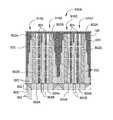
- FIG. 2Ais a schematic top view of a portion of an input device 295 that illustrates a portion of a sensor electrode pattern that may be used to sense the positional information of an input object within the sensing region 120 using a transcapacitive sensing method.
- the input device 295may be formed as part of a larger input device 100 , which is discussed above.
- the sensor electrode pattern disclosed hereincomprises a sensor array set 200 that includes a plurality of sensor electrode arrays 210 that include a plurality of sensor electrodes, such as sensor electrodes 202 and 211 , that are arranged and interconnected in a desirable manner to reduce or minimize the number of traces and/or sensor electrodes required to sense the positional information of an input object within the sensing region 120 of the input device 295 .
- FIG. 2Aillustrates a pattern of simple rectangles used to represent the sensor electrodes, this configuration is not meant to be limiting and in other embodiments, various other sensor electrode shapes may be used as discussed further herein.
- sensing elements 121comprise two or more sensor electrodes, for example, sensor electrodes 202 and 211 that may be similar or different in size and/or shape.
- these sensor electrodesare disposed in a sensor electrode pattern that comprises a first plurality of sensor electrodes 202 (e.g., 15 shown) and a second plurality of sensor electrodes 211 (e.g., 30 shown), which are disposed on the same layer as the first plurality of sensor electrodes 202 .
- Sensor electrodes 202 and sensor electrodes 211are typically ohmically isolated from each other, by use of insulating materials or a physical gap formed between the electrodes to prevent them from electrically shorting to each other.
- two or more sensing elements 121may form a larger unit cell 122 .
- a unit cell 122includes a grouping of sensor electrodes that are repeated within a sensor electrode array 210 and/or in a repeating pattern across the sensing region 120 (e.g., multiple sensor electrode arrays 210 ).
- the unit cell 122is the smallest unit a symmetric grouping of sensor electrodes can be broken into within an electrode pattern formed across the sensing region 120 .
- the unit cell 122includes two sensing elements 121 , which each contain a portion of the sensor electrode 202 and the sensor electrode 211 , and thus the unit cell 122 comprises a sensor electrode 202 and two sensor electrodes 211 .
- sensor electrode pattern of FIG. 2Amay alternatively utilize various sensing techniques, such as mutual capacitive sensing, absolute capacitive sensing, elastive, resistive, inductive, magnetic acoustic, ultrasonic, or other useful sensing techniques, without deviating from the scope of the invention described herein.
- Sensor electrode 202maybe be a transmitter and 211 maybe a receiver, or vice versa (the other way around) with typically similar imaging capability.
- the sensing elements 121may comprise a plurality of transmitter and receiver electrodes that are formed in a single layer on a surface of a substrate 209 .
- each of the sensor electrodesmay comprise one or more transmitter electrodes (e.g. sensor electrodes 202 ) that are disposed proximate to one or more receiver electrodes (e.g. sensor electrodes 211 ).
- a transcapacitive sensing method using the single layer sensor electrode designmay operate by detecting the change in capacitive coupling between one or more of the driven transmitter sensor electrodes and one or more of the receiver electrodes, as similarly discussed above.
- the transmitter and receiver electrodesmay be disposed in such a way such that jumpers and/or extra layers used to form the area of capacitive pixels are not required.
- the transmitter electrodes and receiver electrodesmay be formed in an array on the surface of a substrate 209 by first forming a blanket conductive layer on the surface of the substrate 209 and then performing an etching and/or patterning process (e.g., lithography and wet etch, laser ablation, etc.) that ohmically isolates each of the transmitter electrodes and receiver electrodes from each other.
- the sensor electrodesmay be patterned using deposition and screen printing methods. As illustrated in FIG.
- these sensor electrodesmay be disposed in an array that comprises a rectangular pattern of sensing elements 121 , which may comprise one or more transmitter electrodes and one or more receiver electrodes.
- the blanket conductive layer used to form the transmitter electrodes and receiver electrodescomprises a thin metal layer (e.g., copper, aluminum, etc.) or a thin transparent conductive oxide layer (e.g., ATO, ITO, Zinc oxide) that is deposited using convention deposition techniques known in the art (e.g., PVD, CVD).
- patterned isolated conductive electrodese.g., electrically floating electrodes
- the sensor electrodesare formed from a material that is substantially optically clear, and thus, in some configurations, can be disposed between a display device and the input device user.
- the areas of localized capacitive coupling formed between at least a portion of one or more sensor electrodes 202 and at least a portion of one or more sensor electrodes 211may be termed a “capacitive pixel,” or also referred to herein as the sensing element 121 .
- the capacitive coupling in a sensing element 121may be created by the electric field formed between at least a portion of the sensor electrodes 202 and a sensor electrode 211 , which changes as the proximity and motion of input objects across the sensing region changes.
- the sensing elements 121are “scanned” to determine these capacitive couplings.
- the input device 295may be operated such that one transmitter electrode transmits at one time, or multiple transmitter electrodes transmit at the same time. Where multiple transmitter electrodes transmit simultaneously, these multiple transmitter electrodes may transmit the same transmitter signal and effectively produce an effectively larger transmitter electrode, or these multiple transmitter electrodes may transmit different transmitter signals.
- the transmitter electrodesare the sensor electrodes 202 and the receiver electrodes are the sensor electrodes 211 .
- multiple sensor electrodes 202transmit different transmitter signals according to one or more coding schemes that enable their combined effects on the resulting signals received by the receiving sensor electrodes, or sensor electrodes 211 , to be independently determined.
- the direct effect of a user input which is coupled to the devicemay affect (e.g. reduce the fringing coupling) of the resulting signals.
- a floating electrodemay be coupled to the input and to the transmitter and receiver and the user input may lower its impedance to system ground and thus reduce the resulting signals.
- a floating electrodemay be displaced toward the transmitter and receiver which increases their relative coupling.
- the receiver electrodes, or a corresponding sensor electrode 211may be operated singly or multiply to acquire resulting signals created from the transmitter signal.
- the resulting signalsmay be used to determine measurements of the capacitive couplings at the capacitive pixels, which are used to determine whether an input object is present and its positional information, as discussed above.
- a set of values for the capacitive pixelsform a “capacitive image” (also “capacitive frame” or “sensing image”) representative of the capacitive couplings at the pixels.
- the sensing image, or capacitive imagecomprises data received during a process of measuring the resulting signals received with at least a portion of the sensing elements 121 distributed across the sensing region 120 .
- the resulting signalsmay be received at one instant in time, or by scanning the rows and/or columns of sensing elements distributed across the sensing region 120 in a raster scanning pattern (e.g., serially polling each sensing element separately in a desired scanning pattern), row-by-row scanning pattern, column-by-column scanning pattern or other useful scanning technique.
- the rate that the “sensing image” is acquired by the input device 100or sensing frame rate, is between about 60 and about 180 Hertz (Hz), but can be higher or lower depending on the desired application.
- the sensing elements 121are disposed on a substrate of an associated display device.
- the sensor electrodes 202 and/or the sensor electrodes 211may be disposed on a polarizer, a color filter substrate, or a glass sheet of an LCD.
- the sensor electrodes 202 and 211may be disposed on a TFT (Thin Film Transistor) substrate of an LCD type of the display device, a color filter substrate, on a protection material disposed over the LCD glass sheet, on a lens glass (or window), and the like.
- the electrodesmay be separate from and in addition to the display electrodes, or shared in functionality with the display electrodes. Similarly, an extra layer may be added to a display substrate or an additional process such as patterning applied to an existing layer.
- the sensing elements 121are disposed on a substrate of a touchpad.
- the sensor electrodes in each sensing element 121 and/or the substratemay be substantially opaque.
- the substrate and/or the sensor electrodes of the sensing elements 121may comprise a substantially transparent material.
- the sensor electrodesmay be comprised of a substantially transparent material (e.g., ATO, ClearOhmTM) or they may be comprised of an opaque material and aligned with the pixels of the display device. Electrodes may be considered substantially transparent in a display device if their reflection (and/or absorption) of light impinging on the display is such that human visual acuity is not disturbed by their presence. This may be achieved by matching indexes of refraction, making opaque lines narrower, reducing fill percentage or making the percentage of material more uniform, reducing spatial patterns (e.g. moire') that are with human visible perception, and the like.
- a substantially transparent materiale.g., ATO, ClearOhmTM
- Electrodesmay be considered substantially transparent in a display device if their reflection (and/or absorption) of light impinging on the display is such that human visual acuity is not disturbed by their presence. This may be achieved by matching indexes of refraction, making opaque lines narrower, reducing fill percentage or making the percentage of material more
- the processing system 110 of the input device 295comprises a sensor controller 218 that is coupled through connectors 217 to each of the transmitter and receiver electrodes, such as sensor electrodes 202 and 211 , through one or more traces (e.g., traces 212 and 213 ) respectively.
- the sensor controller 218is generally configured to transmit the transmitter signal and receive the resulting signals from receiver electrodes.
- the sensor controller 218is also generally configured to communicate the positional information received by the sensing elements 121 to the electronic system 150 and/or the display controller 233 , which is also coupled to the electronic system 150 .
- the sensor controller 218may be coupled to the electronic system 150 using one or more traces 221 that may pass through a flexible element 251 and be coupled to the display controller 233 using one or more traces 221 A that may pass through the same flexible element 251 or a different connecting element, as shown. While the processing system 110 illustrated in FIG. 2A schematically illustrates a single component (e.g., IC device) to form the sensor controller 218 , the sensor controller 218 may comprise two or more controlling elements (e.g., IC devices) to control the various components in the processing system 110 of the input device 295 . The controller devices may be placed onto display substrates such as TFT or Color Filter/Sealing layers (e.g. as a Chip On Glass).
- the functions of the sensor controller 218 and the display controller 233may be implemented in one integrated circuit that can control the display module elements and drive and/or sense data delivered to and/or received from the sensor electrodes. In various embodiments, calculation and interpretation of the measurement of the resulting signals may take place within the sensor controller 218 , display controller 233 , a host electronic system 150 , or some combination of the above.
- the processing system 110may comprise a transmitter circuitry, receiver circuitry, and memory that is disposed within one or any number of ICs found in the processing system 110 , depending to the desired system architecture.
- FIG. 2Bis a schematic view of a portion of the processing system 110 of the input device 295 according to one or more of the embodiments described herein.
- the sensor controller 218includes a signal generating processor 255 and sensor processor 256 that work together to provide touch sensing data to an analysis module 290 and the electronic system 150 .
- the analysis module 290may be part of the processing system 110 , the sensor processor 256 and/or part of the electronic system 150 .
- the analysis module 290will comprises digital signal processing elements and/or other useful digital and analog circuit elements that are connected together to process the receiver channel output signal(s) received from at least one receiver channel that is coupled to a receiver electrode, and also provide processed signals to other portions of the electronic system 150 .
- the electronic system 150can then use the processed signals to control some aspect of the input device 295 , such as send a message to the display, perform some calculation or software related task based on instructions created by one or more software programs that are being run by the electronic system and/or perform some other function.
- the processing system 110may comprise a signal generating processor 255 and a sensor processor 256 that work together to provide receiver channel output signals to the analysis module 290 and/or the electronic system 150 .
- the positional information of an input object 140is derived based on the capacitance C s (e.g., capacitance C S1 , C S2 , C SN ) measured between each of the transmitter electrodes (e.g., sensor electrodes 202 1 , 202 2 , . . . 202 N ) and the receiver electrodes (e.g., sensor electrodes 211 1 , 211 2 , . . . 211 N ).
- the signal generating processor 255comprises a driver 228 , which are adapted to deliver capacitive sensing signals (transmitter signals) to the transmitter electrodes.
- the driver 228may comprise a power supply and signal generator 220 that is configured to deliver a square, rectangular, trapezoidal, sinusoidal, Gaussian or other shaped waveforms used to form the transmitter signal(s) to the transmitter electrodes.
- the signal generator 220comprises an electrical device, or simple switch, that is able to deliver a transmitter signal that transitions between the output level of the power supply and a low display voltage level.
- signal generator 220may comprise an oscillator.
- the signal generator 220is integrated into the driver 222 , which includes one or more shift registers (not shown) and/or switches (not shown) that are adapted to sequentially deliver transmitter signals to one or more of the transmitter electrodes at a time.
- the sensor processor 256comprises a plurality of receiver channels 275 (e.g., receiver channels 275 1 , 275 2 , . . . 275 N ) that each have a first input port 241 (e.g., ports 241 1 , 241 2 , . . . 241 N ) that is configured to receive the resulting signal received with at least one receiver electrode (e.g., sensor electrode 211 1 , 211 2 , . . . 211 N ), a second input port (e.g., ports 242 1 , 242 2 , . . .
- each receiver channel 275is coupled to a single receiver electrode.
- Each of the plurality of receiver channels 275may include a charge accumulator 276 (e.g., charge accumulators 276 1 , 276 2 , . . . 276 N ), supporting components 271 (e.g., components 271 1 , 271 2 , . . . 271 N ) such as demodulator circuitry, a low pass filter, sample and hold circuitry, other useful electronic components filters and analog/digital converters (ADCs) or the like.
- charge accumulator 276e.g., charge accumulators 276 1 , 276 2 , . . . 276 N
- supporting components 271e.g., components 271 1 , 271 2 , . . . 271 N
- demodulator circuitrye.g., components 271 1 , 271 2 , . . . 271 N
- ADCsanalog/digital converters
- the analog/digital convertermay comprise, for example, a standard 8, 12 or 16 bit ADC that is adapted to receive an analog signal and deliver a digital signal (receiver channel output signal) to the analysis module 290 (e.g. a Successive Approximation ADC, a Sigma-Delta ADC, an Algorithmic ADC, etc).
- the charge accumulator 276includes an integrator type operational amplifier (e.g., Op Amps A 1 -A N ) that has an integrating capacitance C fb that is coupled between the inverting input and the output of the device.
- the cost required to form the each receiver channel 275is generally more expensive than the cost required to form the components in the signal generating processor 255 that provides the transmitter signal(s) to a transmitter electrode(s).
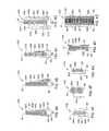
- FIG. 3Ais a table that lists examples of various different sensing electrode connection configurations that can be used to form an array of transcapacitive sensing elements that are used to sense the positional information of an input object that is positioned over at least a portion of the array. Each row of the table contains a different sensing electrode configuration that can be advantageously used in one or more of the embodiments described herein.
- FIG. 3Bschematically illustrates the first sensing electrode configuration found in the table shown in FIG. 3A (e.g., first row of the table), which has one transmitter electrode 312 (or transmitters Tx) and twelve receiving electrodes 311 (or receivers Rx) that are used to detect the positional information of an input object disposed over the array 310 of sensing elements.
- each of the receiving electrodes 311can be separately poled by a sensor controller 218 ( FIG. 2A ) by use of its dedicated trace 304 (e.g., 12 traces are shown in FIG. 3B ) when a transmitter signal is delivered through the transmitter electrode 312 via its dedicated trace 303 .
- Each of the receiving electrodes 311 and traces 304 and transmitter electrode 312 and trace 303may be coupled to one or more components in the processing system 110 , such as the sensor controller 218 .
- the traces 303 and 304are generally similar to the traces 212 and 213 , respectively, which were discussed above. In this way, each receiving electrode 311 and at least an adjacently positioned portion of transmitter electrode 312 form a sensing element 121 ( FIGS.
- FIG. 3Bcan also be used to illustrate the sixth configuration disclosed in the table (e.g., 12 transmitters and 1 receiver) by swapping the function of the electrodes 311 and 312 from receiver electrodes to transmitter electrodes and transmitter electrode to receiver electrode, respectively.
- the capacitive coupling between electrodesis typically symmetric in most materials.
- FIG. 3Cschematically illustrates the fourth sensing electrode configuration found in the table shown in FIG. 3A , which has four transmitter electrodes 312 and three receiving electrode elements 311 A- 311 C that are all used to detect the positional information of an input object disposed over the array 310 of sensing elements illustrated in FIG. 3C .
- each of the receiving electrode elements 311 A, 311 B and 311 Ccan be separately polled by a sensor controller 218 by use of its dedicated trace 304 (e.g., 3 traces are shown in FIG. 3C ) when a transmitter signal is delivered through one of the transmitter electrodes 312 via its dedicated trace 303 .
- the sensing region 120still contains the same number of sensing elements 121 as the configuration shown in FIG. 3B .
- the first sensor electrode element in the receiving electrode elements 311 Awhich is adjacently positioned relative to the top transmitter electrode 312 in FIG.
- FIG. 3Cforms one sensing element 121 , and the other receiving electrode elements 311 A that is adjacently positioned relative to the second transmitter electrode 312 from the top in FIG. 3C will also form another sensing elements 121 , and so on for the other receiving electrodes and transmitting electrodes.
- FIG. 3Ccan also be used to illustrate the third configuration disclosed in the table (e.g., 3 transmitters and 4 receiver) by swapping the function of the electrodes 311 and 312 from receiver electrodes to transmitter electrodes and transmitter electrode to receiver electrode, respectively.
- the electrodes 311 , 312 in the array 310 shown in FIG. 3Cit will only require 7 total traces, which are contained in the group of traces 305 B. In the simple example illustrated in FIG. 3C , the total number of traces can be can be reduced by about 46% from the configuration illustrated in FIG. 3B .
- the benefit of reducing the number of traces used in an input deviceis generally important in reducing the complexity and cost of the input device, since the sensing region 120 of most typical 3 inch up to 15 inch diagonal handheld devices today, such as a tablet, PDA or other similar device, require hundreds or even thousands of sensing elements 121 to reliably sense the position of one or more input objects, such as fingers.
- the reduction in the number of traces that need to be routed to the various processing system 110 componentsis desirable for a number of reasons, which include a reduction in the overall cost of forming the input device 100 , a reduction in the complexity of routing the multitude of traces 303 and 304 within the sensing region 120 , a reduced interconnecting trace length due to reduced routing complexity, a reduction in the cross-coupling of signals between adjacently positioned traces, and allowing for a tighter packing or increased density of electrodes 311 and 312 within the sensing region 120 .
- the reduction in the number of traceswill also reduce the amount of cross-coupling between the traces due to a reduction in the required trace density and number of traces that will transmit or receive signals delivered to or from adjacently positioned sensor electrodes or traces.
- one or more of the embodiments described hereinutilizes one or more of the techniques and electrode array configuration disclosed herein to reduce or minimize the number of traces and/or electrodes required to sense the position of an input object within the sensing region 120 . Reducing the number of electrodes may allow designs that significantly reduce cost and complexity to be created, even when a larger number of receiver electrodes are required.
- the receiver channels 275may include a charge accumulator 276 and supporting components 271 , such as demodulator circuitry, a low pass filter, sample and hold circuitry, other useful electronic components filters and analog/digital converters (ADCs), while the transmitter signals can be created and delivered by use of a signal generator 220 and one or more shift registers and/or simple electrical switches.
- the number of transmitter electrodesis greater than the number of receiver electrodes, such as the configurations 4-6 listed in the table found in FIG. 3A .
- the number of receiver electrodessuch as the configurations 4-6 listed in the table found in FIG. 3A .
- an electrodee.g., sensor electrodes 301 , 311 , 302 , 312 , etc.
- a tracemay also contain connecting elements that are used to interconnect multiple sensor electrode elements together to form a sensor electrode, such as the interconnecting trace elements 304 A that are each used to connect the receiving electrode elements 311 A together, as illustrated in FIG. 3C .
- each tracehas a physical size that allows the delivered transmitter signals and/or received resulting signals to be transmitted from the sensor electrode element portion of the sensor electrode to the various processing system 110 components.
- each tracehas a length and a cross-sectional area, which is defined by its thickness multiplied by its width, which both can be adjusted to assure that the resistance of this interconnecting component does not cause significant variation in the transmission or receipt of the capacitive sensing signals by the processing system 110 components.
- the cross-sectional area of each traceis adjusted to compensate for the different lengths of the traces to assure that the resistance loss for each electrode is similar, no matter how close or far the electrode is from the various processing system components.
- FIGS. 4A-17Beach illustrate the various configurations of sensing electrodes that can be used in conjunction with the processing system 110 components discussed above to determine the positional information of an input object that is disposed within the sensing region 120 .
- the sensor electrode configurations illustrated in FIGS. 4A-17Bare illustrated in FIGS.
- 4A-4K , 5 A- 5 C, 8 and 14include a plurality of sensor electrodes that are configured to form a sensor electrode array (e.g., sensor electrode array 210 , 310 A- 310 K, 510 A- 510 K, etc.) that can be used as part of a larger sensor array set (e.g., sensor array set 200 , 600 , 650 , 700 , 900 A, 900 B, 1000 , etc.), which is used to sense the positional information of an input object that is disposed within the sensing region 120 of an input device 100 . While the sensor electrode configurations illustrated in FIGS.
- the sensing electrodescan be disposed in an array of sensing electrodes, such as, for example, the sensing electrode arrays 310 A- 310 K in FIGS. 4A-4K , sensing electrode arrays 510 A- 510 C in FIGS. 5A-5C and sensing electrode array 810 in FIG. 8 , which in some cases may be positioned in larger sensor array sets that include arrays of sensing electrodes, such as the sensor array sets shown in FIGS.
- Embodiments of the inventioncan be used to create a capacitive image using only sensor electrodes in a single layer disposed on a surface of a substrate. In some embodiments, no sensor electrodes are layered or jumpered within the sensing region 120 , which is used for capacitive sensing.
- the sensor electrodes described hereincan, for example, be formed by patterning a blanket conductive layer comprising a thin metal layer (e.g., copper, aluminum, etc.) or a thin transparent conductive oxide layer (e.g., ATO, ITO, AZO) that is deposited on a surface of an optically clear substrate (e.g., glass), or in some cases optically opaque substrate, using convention deposition techniques known in the art (e.g., PVD, CVD, evaporation, sputtering, etc.).
- a blanket conductive layercomprising a thin metal layer (e.g., copper, aluminum, etc.) or a thin transparent conductive oxide layer (e.g., ATO, ITO, AZO) that is deposited on a surface of an optically clear substrate (e.g., glass), or in some cases optically opaque substrate, using convention deposition techniques known in the art (e.g., PVD, CVD, evaporation, sputtering, etc.).
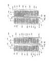
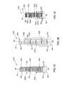
- FIGS. 4A and 4Beach illustrate a portion of a sensor electrode pattern, or array of sensor electrodes 310 A and 310 B, respectively, that may be used to form a single layer capacitive imaging sensor.
- FIG. 4Aillustrates a plurality conductive routing traces, where sensor electrodes 301 and 302 A- 302 E are coupled to processing system 110 through one of the traces 303 and 304 .
- a sensor electrode 301may be patterned around a plurality of sensor electrodes 302 A- 302 E.
- the traces 303 and/or 304may all be routed to one side of sensor electrode pattern as illustrated in FIG. 4B or to different sides as illustrated in FIG.
- the traces 303 and/or 304may be routed to different sides of an array of sensor electrodes 310 A, as illustrated in FIG. 4A , to assure that multiple arrays of sensor electrodes 310 A (see FIG. 6A ) can be closely spaced together and reduce the possibility that electric fields created by the signal transmission through the traces (e.g., traces 303 ) will affect the measured resulting signal received by one or more of the electrodes found in an adjacently positioned array of sensor electrodes.
- the number of sensor electrodesmay be adjusted to achieve a desired capacitive sensing resolution, pixel response and/or size of the sensor.
- size of an electrode or traceis generally intended to signify the difference in surface area of the electrode that is parallel to the surface that the electrode or trace is positioned on, since the thickness of the material used to form the electrodes and/or traces is typically small compared to the electrode's or trace's dimensions parallel to the surface on which it is positioned, and will remain relatively constant across the entire sensing region 120 .
- each type of electrodei.e., transmitter or receiver
- Rratio of the sizes of the electrodes
- sensor electrodes that are configured as transmitter electrodese.g., sensor electrode 802 A in FIG.
- an adjacent edge(s)e.g., right side vertical edge
- the sum of the adjacent edges of the adjacently positioned receiver electrodese.g., left side vertical edges of the sensor electrode elements 801 A and 805 A in FIG. 8 ).
- the sensor electrode 301may be patterned so that it can capacitively couple with each sensor electrode, such as the sensor electrodes 302 (e.g., sensor electrodes 302 A- 302 E in FIG. 4A ).
- sensor electrodes 301 and 302 and the traces 303 , 304may comprise a similar material that is disposed over a surface of a substrate.
- sensor electrodes 301 and 302may comprise a first material and the traces 303 , 304 may comprise a second material, wherein the first and second materials are different.
- the sensor electrodes and conductive routing tracesmay comprise substantially transparent materials or substantially optically invisible materials such as Indium Tin Oxide (ITO), thin metal wires or the like.
- ITOIndium Tin Oxide
- the sensor electrode 301may be configured to perform as a transmitter electrode and sensor electrodes 302 may be configured to perform as receiver electrodes. In other cases, the sensor electrode 301 may be configured to perform as a receiver electrode and sensor electrodes 302 may be configured to perform as transmitter electrodes.
- the processing system 110is configured to simultaneously receive resulting signals from sensor electrodes 302 while transmitting a transmitter signal from the sensor electrode 301 . In other embodiments, processing system 110 is configured to sequentially transmit transmitter signals through each of the sensor electrodes 302 while receiving resulting signals using the sensor electrode 301 .
- sensor electrode 301is patterned around each of the sensor electrodes 302 A- 302 E. In some embodiments, the sensor electrode 301 is patterned in such a way that it at least partially encloses each of the sensor electrodes 302 .
- the term “partially enclose,” as used herein,is intended to describe a configuration where a portion of a first type of sensor electrode is disposed around a significant portion of the linear length of an edge or edges that define, or outline, the area of a second type of sensor electrode.
- a first type of sensor electrodeis said to partially enclose a second type of sensor electrode, where the first type of sensor electrode is disposed around the periphery of a second type of sensor electrode so that the centroid of the area of the second type of sensor electrode is at least disposed between opposing portions of the partially enclosing part of first type of electrode, while still allowing routing of the separate electrodes in a single layer.
- 4Gis said to partially enclose the sensor electrode 302 A, since it is disposed around a significant portion of the sensor electrode 302 A, so that the centroid of the area (not shown) of the sensor electrode 302 A (triangular shaped electrode) is disposed between the top two segments of the sensor electrode 301 , which are adjacent to two of the three edges of the sensor electrode 302 A.
- the sensor electrode 301is designed to meander around and between the sensor electrodes 302 A- 302 E, so that the conductive path that the electrode forms, between the connection side of the sensor electrode 301 , which is coupled to the trace 304 , and the furthest point away from the connection side (e.g., near sensor electrode 302 A), winds back and forth around a central axis (e.g., a vertical axis of symmetry in FIG. 4A (not shown)) in which the array of sensor electrodes 310 A are aligned.
- a central axise.g., a vertical axis of symmetry in FIG. 4A (not shown) in which the array of sensor electrodes 310 A are aligned.
- the meander of the sensor electrode 301may also wind around portions of each of the sensor electrodes 302 A- 302 E to at least partially enclose each electrode. While a portion of the sensor electrode 301 is illustrated as being disposed between each adjacent pair of sensor electrodes 302 A- 302 B, 302 B- 302 C, etc. in FIG. 4A , this configuration is not intended to be limiting, since the meander of the sensor electrode 301 need not pass between each pair of adjacent sensor electrodes 302 A- 302 B, etc. and may only pass between one of the adjacently positioned pairs in the sensor electrode array 310 A.
- the length of the sensor electrode 301may be desirable to maximize the length of the sensor electrode 301 to improve its sensitivity in receiving or transmitting a capacitive sensing signal between one or more of the adjacently positioned sensor electrodes 302 A- 302 E.
- the sensor electrode 301may be similar in size to the trace 304 and comprise the same material as the material used to form each sensor electrode element 302 A- 302 E (e.g., layer of ITO), and thus may be formed during the patterning process used to form the sensor electrode elements.
- the sensor electrode array 310 Aincludes a first type of sensor electrodes, such as sensor electrodes 302 A- 302 E that have a first sensor electrode shape (e.g., polygonal shape), that are at least partially enclosed by a second type of sensor electrode that has a second sensor electrode shape (e.g., wire shaped), which is different than the first sensor electrode shape.
- the sensor electrode array 310 Aincludes sensor electrodes 302 A- 302 E that have a polygonal shape, and are at least partially enclosed by a second type of sensor electrode 301 that has a shape that outlines the polygonal shape of the sensor electrodes 302 A-E.
- a shape of a sensor electrode that is spaced a repeatable or common distance from, or outlines, at least a portion of another sensor electrodeis also defined herein as an electrode that has a complementary shape, or is a complementary shaped electrode.
- the sensor electrode 301may have a complementary shape, which is rectangular, that outlines the rectangular shaped sensor electrodes 302 A-E.
- the sensor electrode 301may have a meandering shape that has a differing orientation for each of the one or more of the adjacently positioned sensor electrodes 302 A- 302 E.
- the uppermost portion of the sensor electrode 301has a C-shaped orientation that outlines the sensor electrode 302 A, and the adjacent portion of the sensor electrode 301 has an inverted C-shaped orientation (e.g., inverted horizontally) that outlines the sensor electrode 302 B.
- the sensor electrode 301is patterned in such a way that it is disposed around pairs or larger groups of sensor electrodes, such as two or more sensor electrodes 302 A- 302 E. Therefore, the array of sensor electrode configurations illustrated herein are not intended to be limiting as to the scope of the invention described herein, since the sensor electrode 301 can be disposed at least partially around two or more sensor electrodes without deviating from the basic scope of the invention described herein.
- the sensor electrode 301is formed so that the conductive path that the sensor electrode forms, between the connection side of the sensor electrode 301 , which is coupled to the trace 304 , and the furthest position away from the connection side (e.g., near sensor electrode 302 A), is non-meandering and thus has a short path length (e.g., length of the portion of the electrode disposed on the left side of the sensor electrodes 302 A- 302 E in FIG. 4B ).
- the sensor electrode 301has a complementary shape, which is rectangular, that outlines the rectangular shaped sensor electrodes 302 A-E. Further, as shown in FIG.
- the sensor electrode 301may have a shape that has the same orientation for one or more of the adjacently positioned sensor electrodes 302 A- 302 E.
- the uppermost portion of the sensor electrode 301has a C-shaped orientation that outlines the sensor electrode 302 A
- an adjacent portion of the sensor electrode 301also has a C-shaped orientation that outlines the sensor electrode 302 B.
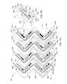
- FIG. 4Cillustrates an array of sensor electrodes 310 C that comprises a sensor electrode 301 that is patterned around the sensor electrodes 302 A- 302 E, which each have a distributed electrode shape, such as a zig-zag wire shape as shown.
- the zig-zag wire shapecan also be formed in a sinusoidal, stepped or other waveform type shape, including irregular wave type shapes.
- use of a distributed electrode shape, as shown in FIG. 4Cmay be preferred over a solid electrode shape, as shown in FIG. 4A , to adjust the ratio of the transmitter and receiver electrode areas by adjusting the sensor electrode area formed in the distributed electrode shape to improve the capacitive sensing sensitivity of the input device.
- the distributed electrode shape type of sensor electrodesmay be formed in various different shapes, orientations, designs and sizes.
- sensor electrodes 302 A- 302 E, and their respective traces 303may be comprised of the same materials and may have a similar cross-sectional size in its zig-zag wire shape.
- the sensor electrode 301has a complementary shape, which is rectangular, that outlines the rectangular peripheral shape of the sensor electrodes 302 A-E.
- FIG. 4Dillustrates an array of sensor electrodes 310 D that comprises a segmented sensor electrode 301 that are each disposed around one or more of the sensor electrodes 302 A- 302 E.
- the array of sensor electrodes 310 Dis similar to the array of sensor electrodes 310 A illustrated in FIG. 4A , except that the sensor electrode 301 of FIG. 4A has been segmented so that groups of one or more sensor electrodes 302 A- 302 E are at least partially enclosed in each of the formed segments 301 A- 301 C. In this way, the different segments 301 A- 301 C of the sensor electrode 301 can be separately polled at the same time or sequentially polled in time by the sensor controller components in the processing system 110 . In one embodiment, as illustrated in FIG.
- the sensor electrode array 310 Dincludes a first type of sensor electrodes, such as sensor electrodes 302 A- 302 E that have a first electrode shape (e.g., polygonal shape), that are at least partially enclosed by a second type of sensor electrodes that have a second electrode shape (e.g., wire shaped).
- a first type of sensor electrodessuch as sensor electrodes 302 A- 302 E that have a first electrode shape (e.g., polygonal shape), that are at least partially enclosed by a second type of sensor electrodes that have a second electrode shape (e.g., wire shaped).
- FIG. 4Eillustrates an array of sensor electrodes 310 E that comprises an open circular or arc shaped sensor electrode 301 that is patterned around one or more of the circular sensor electrodes 302 A- 302 C.
- FIG. 4Fillustrates an array of sensor electrodes 310 F that comprises an open hexagonal shaped sensor electrode 301 that is patterned around one or more of the hexagonal shaped sensor electrodes 302 A- 302 B.
- the sensor electrode 301has a complementary shape, which is circular or hexagonal, that outlines the circular or hexagonal shaped sensor electrodes 302 A-E.
- 4E and 4Fare not intended to limiting, and thus can be oriented in any other desirable orientation.
- a group of several arrays of sensor electrodes 310 E or 310 F(not shown), or sensor array set, may be positioned and oriented so that the adjacently positioned arrays of sensor electrodes 310 E or 310 F form a hexagonal close-packed pattern across the sensing region 120 to improve the density of the sensing electrode pattern.
- FIG. 4Gillustrates an array of sensor electrodes 310 G that comprises a triangular shaped sensor electrode 301 that is disposed between and/or patterned around a portion of one or more of the triangular shaped sensor electrodes 302 A- 302 B.
- the array of sensor electrodes 310 Gshown in FIG. 4G , includes a configuration in which the sensor electrode 301 is disposed adjacent to two edges of each of the sensor electrodes 302 A- 302 C.
- the sensor electrode 301 in FIG. 4Gpartially encloses the sensor electrode 302 A, since it is disposed around a significant portion of the sensor electrode 302 A.
- the sensor electrode array 310 Gincludes sensor electrodes 302 A- 302 E, which have a triangular electrode shape, that are at least partially enclosed by a zig-zag or other similar shaped electrode that is disposed between the sensor electrodes 302 A- 302 E.
- the sensor electrode 301has a complementary shape that outlines at least a portion of the sensor electrodes 302 A-E.
- FIG. 4Hillustrates an array of sensor electrodes 310 H that comprises a sensor electrode 301 that is patterned around one or more complex shaped sensor electrodes 302 A- 302 D. As illustrated in FIG. 4H , the sensor electrode 301 has a complementary shape that outlines at least a portion of the sensor electrodes 302 A-D.
- FIG. 4Iillustrates an array of sensor electrodes 310 I that comprises a sensor electrode 301 that is disposed within one or more of the sensor electrodes 302 A- 302 D.
- FIGS. 4H and 4Ieach generally illustrate sensor electrode configurations that interleave, or are interdigitated with each other in hopes of maximizing the length of the adjacent edges of the sensor electrodes to improve the capacitive coupling between the electrodes.
- FIGS. 4J and 4Keach illustrate a sensor array set 400 J, 400 K, respectively, that include sensor electrode arrays 310 J, 310 K, that each comprises a sensor electrode 301 that is disposed within one or more polygonal shaped sensor electrodes 302 A- 302 D.
- FIG. 4Kdiffers from FIG. 4J in that the traces 303 and 304 in one of the array of sensor electrodes 310 K has been altered to change the symmetry of the electric fields and/or capacitive coupling generated across a portion of the sensing region 120 .
- one or more of the sensor electrode arrayscan be formed in other orientations to alter the position or routing of the sensor electrodes in adjacent sensor electrode arrays (e.g., mirror image of the sensor electrodes 301 and 302 A-D in adjacent sensor electrode arrays) to alter the electric fields formed by the sensor electrodes in the sensor electrode arrays within a sensor array set.
- FIGS. 4J and 4Keach illustrate another possible sensor electrode configuration that has sensor electrodes that interleave, or are interdigitated with, each other to maximize the length of the adjacent edges of the sensor electrodes to improve the capacitive coupling between the electrodes. This can optimize the ratio of user input signal relative to the direct coupling (e.g. of interference) of an input into either electrode.
- the sensor electrode array 310 I-Kincludes a first type of sensor electrodes, such as sensor electrodes 302 A- 302 F that each have a first electrode shape (e.g., polygonal shape) that includes a plurality of recessed regions 391 in which a portion of a second type of sensor electrode (e.g., sensor electrode 301 ) is disposed.
- first electrode shapee.g., polygonal shape
- second type of sensor electrodee.g., sensor electrode 301
- the gap formed between the edge of the first type of sensor electrodes and the second type of sensor electrodes in the recessed region 391is small enough to assure ohmic isolation and sized to achieve a desirable capacitive coupling between the sensor electrodes.
- the sensor electrode 301has a back-bone shape that includes a plurality of fingers 392 , which are arrayed in a pattern and are interconnect by one or more connecting segments 393 .
- FIG. 5Aillustrates an alternative embodiment of a of sensor electrode array 510 A that includes a plurality of sensor electrodes 301 and 302 A- 302 E of a single layer capacitive sensor device that are positioned to form interdigitated sensor electrodes.
- sensor electrode 301is interdigitated with sensor electrodes 302 A- 302 E, such that one or more electrode segments 501 of each of the sensor electrodes 302 A- 302 E and electrode segments 502 of each of the one or more sensor electrode(s) 301 overlap in at least one direction (e.g., horizontal direction in FIG. 5A ).
- FIG. 5Aillustrates an alternative embodiment of a of sensor electrode array 510 A that includes a plurality of sensor electrodes 301 and 302 A- 302 E of a single layer capacitive sensor device that are positioned to form interdigitated sensor electrodes.
- sensor electrode 301is interdigitated with sensor electrodes 302 A- 302 E, such that one or more electrode segments 501 of each of the sensor electrodes 302 A- 30
- the sensor electrode 301has a meandering configuration that also includes the sensor electrode 301 that at least partially encloses each of the sensor electrodes 302 A- 302 E.
- the meandering configurationmay also include a sensor electrode 301 that weaves between one or more the adjacent sensor electrodes 302 A-E, as well as at least partially enclosing one or more of the sensor electrodes 302 A- 302 E This sensor electrode configuration will tend to maximize the length of the adjacent edges of the sensor electrodes 301 and 302 to improve the capacitive coupling between each pair of sensor electrodes in each sensing element 121 (e.g., sensor electrode 302 A and a portion of sensor electrode 301 ).
- the sensor electrodes 301 and 302may be interdigitated or interleaved in various other orientations.
- FIG. 5Billustrates an array of sensor electrodes 510 B.
- a vertical orientationsuch as the interdigitated electrode segments 506 and 505 of the sensor electrodes 301 and 302 , respectively, may be used.
- sensor electrode 301is interdigitated with sensor electrodes 302 A- 302 E, such that one or more electrode segments 505 of each of the sensor electrodes 302 A- 302 E and electrode segments 506 of each of the one or more sensor electrode(s) 301 overlap in one direction (e.g., vertical direction in FIG. 5 B).
- one directione.g., vertical direction in FIG. 5 B.
- FIG. 5Cillustrates another embodiment of an interdigitated single layer sensor electrode pattern, or array of sensor electrodes 510 C.
- a sensor electrode 301is interdigitated with sensor electrodes 302 A- 302 H.
- two different sensor electrodes 302are interdigitated with a portion of sensor electrode 301
- a single sensor electrode 302is interdigitated with that same portion of sensor electrode 301 in the embodiment illustrated in FIG. 5A .
- more than two sensor electrodes 302may be interdigitated with each portion of sensor electrode 301 .
- FIG. 6Aschematically illustrates a sensor array set 600 , which may comprise two or more sensor electrode arrays 610 .
- the four sensor electrodes arrays 610are disposed within a sensing region 120 to determine the positional information of an input object by use of a capacitive sensing technique.
- the sensor electrode arrays 610may be similar to the sensor electrode array 310 A illustrated in FIG. 4A , as shown, or in any other similar sensor array configuration as shown in FIGS. 4B-4K and 5 A- 5 B or variants thereof.
- each of the traces 303 and 304may be coupled to the sensor controller 218 ( FIG. 2A ) so that the sensors in the sensor array set can be driven for capacitive sensing.
- the traces 303 and 304may form part of or replace the traces 212 and 213 , respectively, discussed above in conjunction with FIGS. 2A-2B .
- the sensor electrodes 302 A- 302 E in the sensor electrode arrays 610may be used as transmitter electrodes and the sensor electrodes 301 may be used as receiver electrodes.
- the input device containing the sensor electrode arrays 610may be operated such that one transmitter electrode transmits at one time, or multiple similarly positioned transmitter electrodes transmit at the same time.
- multiple sensor electrodes 302 A- 302 E in each sensor electrode array 610transmit different transmitter signals according to one or more coding schemes that enable their combined effects on the resulting signals received by the receiving type sensor electrodes 301 , to be independently determined.
- the receiver type sensor electrodes 301may be operated singly or multiply to acquire resulting signals created from the transmitter signal to determine measurements of the capacitive couplings at the capacitive pixels, which are used to determine whether an input object is present and its positional information, as discussed above.
- the resulting signalsmay be received at one instant in time, or by scanning the each of the various sensing elements distributed across the sensing region 120 or other useful scanning technique.
- FIG. 6Bschematically illustrates a sensor array set 650 , which comprises two or more sensor electrode arrays 610 .
- the sensor array set 650is similar to the sensor array set 600 shown in FIG. 6A , but includes a configuration that contains a shield electrode 670 and trace routing scheme that allows the interconnection of the various traces and external components to be made outside of the sensing region 120 , such as in the external regions 661 and 662 .
- a shield electrode 670 and trace routing schemethat allows the interconnection of the various traces and external components to be made outside of the sensing region 120 , such as in the external regions 661 and 662 .
- the routing of the traces 303 and 304exit two sides of the sensing region 120 . While its generally desirable to have the traces be routed out a single side of the sensing region 120 for ease of forming connections with other external components and reducing the required overall size of the substrate (e.g., substrate 209 in FIG. 2A ) on which the sensor electrodes are disposed, a two or more sided trace routing scheme may be needed as the density or pattern of the sensor electrodes in the sensor electrode arrays 610 or sensor array set 650 becomes more complex. While routing of the traces out of more than one side of the sensing region 120 is only illustrated in FIG. 6B , one skilled in the art will appreciate that any of the other configurations of sensor array sets or variations thereof may benefit from this type of trace routing configuration.
- the shield electrode 670(or guard electrode) is disposed over portions of the surface on which the sensor electrodes 301 and 302 A- 302 J are formed.
- the shield electrode 670which are similarly labeled in the figures discussed below as reference numerals 770 , 970 , 1070 , 1270 , 1570 and 1670 , is generally used to shield the sensor electrodes and associated conductive traces 303 and 304 from each other to prevent or minimize the cross-talk between adjacently positioned and closely spaced traces and/or sensor electrodes.
- the shield electrode 670may be coupled to a substantially constant voltage such as system ground, or any other substantially constant voltage, or varying voltage, which is able to shield nearby sensor electrodes and traces from each other.
- the shield electrode 670is useful to help improve the coupling of the input object 140 ( FIG. 1 ) to the input device's ground, and thus reduce the often large variability seen in the capacitive sensing measurements collected when the chassis of the input device 100 , such as a cell phone, is not in sufficient electrical contact with the input object, such as the finger of the input device user.
- the shield electrode 670may comprise one or multiple electrodes either coupled to one another or driven with a similar signal (e.g., system ground).
- a similar signale.g., system ground
- one or more portions of the shield electrode 670may be coupled together in the external regions 661 and 662 , and connected to an input device 100 system ground and/or chassis of the input device 100 by a trace 605 .
- the material from which the shield electrode is formedis the same as the material from which the sensor electrodes are formed, and thus in some embodiments, can be formed out of the same blanket layer of material during the sensor electrode patterning process.
- the sensor electrodes, shield electrode(s) and conductive routing tracesmay comprise substantially transparent materials or substantially optically invisible materials such as Indium Tin Oxide (ITO), thin metal wires, metal layer or the like.
- ITOIndium Tin Oxide
- FIG. 7schematically illustrates a sensor array set 700 , which comprises two or more sensor electrode arrays 710 .
- the four sensor electrodes arrays 710are disposed within a sensing region 120 to determine the positional information of an input object by use of the various processing system 110 components that are discussed above.
- the sensor array set 700is similar to the sensor array set 650 shown in FIG. 6B , but includes a sensor array similar to the configurations shown in FIG. 5A .
- the sensor array set 700also includes a shield electrode 770 and trace routing scheme that allows the interconnection of the various traces and external components to be made outside of the sensing region 120 , such as in the external regions 762 .
- FIG. 7schematically illustrates a sensor array set 700 , which comprises two or more sensor electrode arrays 710 .
- the four sensor electrodes arrays 710are disposed within a sensing region 120 to determine the positional information of an input object by use of the various processing system 110 components that are discussed above.
- the sensor array set 700is similar
- the one or more components of the shield electrode 770may be coupled together in the external regions 762 , and also connected to a system ground and/or chassis of the input device 100 by a trace 705 .
- FIGS. 8-17Billustrate various different configurations of sensor electrodes that generally comprise a plurality of sensor electrodes that are arranged in groups of adjacently positioned sensor electrodes that are combined to form an array of sensor electrodes that can be used to form a sensor electrode set.
- Each group of adjacently positioned sensor electrodesmay contain two or more sensor electrodes that are used to form one or more sensing elements 121 .
- one or more of the sensor electrodes in a sensor electrode arraymay be used as a transmitter electrode and one or more of the other sensor electrodes may be used as a receiver electrode.
- the sensor electrodes 802 A- 802 D in one or more of the sensor electrode arraysmay be used as transmitter electrodes and the sensor electrodes 801 and 805 may be used as receiver electrodes.
- the input device containing the sensor electrode arraysmay be operated such that one transmitter electrode transmits at one time, or multiple similarly positioned transmitter electrodes transmit at the same time.
- multiple sensor electrodes 802 A- 802 D in each sensor electrode arraytransmit the same or different transmitter signals.
- the receiver type sensor electrodes 801 and 805may each be operated singly or multiply to acquire the resulting signals to determine measurements of the capacitive couplings at the capacitive pixels (e.g., sensing elements 121 ) to determine the positional information of an input object.
- the resulting signalsmay be received at one instant in time, or by scanning the rows and/or columns of sensing elements distributed across the sensing region 120 in a raster scanning pattern (e.g., serially polling each sensing element separately in a desired scanning pattern), row-by-row scanning pattern, column-by-column scanning pattern or other useful scanning technique.
- FIG. 8illustrates a sensor electrode array 810 that comprises a plurality of sensor electrodes that are arranged in groups of three adjacently positioned sensor electrodes, such as sensor electrodes 801 , 805 and one of the sensor electrodes 802 .
- each group of sensor electrodesis used to form two sensing elements 121 , as shown at the top of FIG. 8 .
- sensor electrodes 802 A- 802 Dare individually coupled to a different trace 803
- sensor electrodes 801 and 805comprise multiple sensor electrode elements 801 A, 805 A that are each coupled together through a common trace 804 A and 804 B, respectively.
- FIG. 8illustrates a sensor electrode array 810 that comprises a plurality of sensor electrodes that are arranged in groups of three adjacently positioned sensor electrodes, such as sensor electrodes 801 , 805 and one of the sensor electrodes 802 .
- each group of sensor electrodesis used to form two sensing elements 121 , as shown at the top of FIG. 8 .
- a sensor electrode element 801 A, 805 A from each sensor electrodeis disposed adjacent a different sensor electrode 802 (e.g., sensor electrodes 802 A- 802 D) within the group.
- each sensor electrode element 801 A, 805 Amay be separately coupled to its own separate trace.
- each of the sensor electrode elementsmay be configured to operate as individual sensor electrodes or as elements of larger sensor electrodes.
- the sensor electrode elements 801 A, 805 Aare illustrated as being part of either the sensor electrode 801 or sensor electrode 805 , in other embodiments the sensor electrode elements may be configured to form any number of sensor electrodes.
- sensor electrodes 802 A- 802 Dmay be configured to transmit transmitter signals and while sensor electrodes 801 and 805 (and related sensor electrode elements) may be configured receive the resulting signals formed from the transmitter signals. Alternately, sensor electrodes 801 and/or 805 may be configured to transmit transmitter signals, while sensor electrodes 802 A- 802 D may be configured to receive the formed resulting signals.
- the sensor electrode elements 801 A and 805 Acan each be coupled together, such that the top sensor electrode element in a portion of each group of sensor electrode elements are coupled together to form the sensor electrode 801 and the bottom sensor electrode element in the portion of the group of sensor electrode elements are coupled together to form the sensor electrode 805 .
- the sensor electrode elementsmay be coupled together in other desirable ways.
- the bottom sensor electrode element adjacent to sensor electrode 802 Amay be coupled to the top sensor electrode element adjacent to sensor electrode 802 B
- the bottom sensor electrode element adjacent to sensor electrode 802 Bmay be coupled to the top sensor electrode element adjacent to sensor electrode 802 C,
- Such a coupling patternmay continue throughout the sensor electrode pattern or it may be varied through the sensor electrode pattern.
- the number of tracesmay be reduced by nearly half, as compared with configurations that have one sensor electrode element for each trace.
- the sensor electrode pattern illustrated in FIGS. 8-17Bmay provide an improved signal to noise ratio and/or provide a capacitive pixel response that is wider which provides increased response to smaller input objects (e.g., smaller than 5 mm) over other more conventional designs.
- the sensor electrode pattern of FIG. 8may provide a connection between the sensor and processing system 110 with a reduced number of interconnecting vias in the flex (a reduction of about fifty percent) (i.e., reference numeral 251 in FIG. 2A ). Further, the sensor electrode pattern of FIG. 8 may provide for an increased capacitive frame rate.
- the number of traces and/or electrodes required to sense the position of an input object within the sensing regioncan be reduced without affecting the accuracy and repeatability of the acquired positional data.
- FIG. 9Aschematically illustrates a sensor array set 900 A, which comprises two or more sensor electrode arrays 910 , such as sensor electrode arrays 910 A- 910 D.
- FIG. 9Bschematically illustrates another sensor array set configuration, or sensor array set 900 B, which comprises two or more sensor electrode arrays 910 .
- Each of the sensor electrode arrays 910 A- 910 D in the sensor array sets 900 A and 900 Bcontain the sensor electrode array 810 shown in FIG. 8 .
- the sensor electrode arrays 910 A- 910 D in the sensor array set 900 Aare oriented so that the sensor electrodes 801 and 805 in adjacent sensor electrode arrays (e.g., sensor electrode arrays 910 A and 910 B) are positioned adjacent to each other, while the sensor electrode arrays 910 A- 910 D in the sensor array set 900 B are each oriented in the same direction.
- the sensor array sets 900 A and 900 Bmay also include a shield electrode 970 and trace routing scheme that allows the interconnection of the various traces and external components to be made outside of the sensing region 120 , such as in the external regions 962 .
- the portions of the shield electrode 970 that are disposed between the sensor electrodes and their associated tracescan help reduce the cross-talk between sensor electrodes, which may be especially useful for configurations that have sensor electrodes of opposing types adjacent to each other, such as shown in FIG. 9B .
- the one or more components of the shield electrode 970may be coupled together in the external regions 962 , and also connected to a system ground and/or chassis of the input device 100 by a trace 905 .
- FIG. 10schematically illustrates a sensor array set 1000 , which comprises two or more sensor electrode arrays 1010 , such as sensor electrode arrays 1010 A- 1010 D.
- Each of the sensor electrode arrays 1010 A- 1010 D in the sensor array set 1000are generally different from the sensor electrode array 810 shown in FIG.
- the sensor electrode elements 801 A and 805 A in each sensor electrode arrayare positioned so that the bottom sensor electrode element 805 A, which is adjacent to a first sensor electrode (e.g., electrode 802 A), is coupled to the top sensor electrode element 805 A that is adjacent to a second sensor electrode (e.g., electrode 802 B), and the bottom sensor electrode element 801 A, which is adjacent to the second sensor electrode, may be coupled to the top sensor electrode element 801 A that is adjacent to a third sensor electrode (e.g., electrode 802 C), and so on, as is shown in FIG. 10 .
- Such a coupling pattern of the sensor electrode elementsmay continue throughout the sensor electrode array or it may be varied through the sensor electrode pattern.
- a capacitive image sensormay comprise a first set of sensor electrodes comprising a first sensor electrode element 801 A, a second sensor electrode element 805 A and a third sensor electrode element 801 A, and the first sensor electrode element 801 A is electrically coupled to the third sensor electrode element 801 A, and a second set of sensor electrodes comprising a fourth sensor electrode 802 A and a fifth sensor electrode 802 B, wherein the fourth sensor electrode 802 A is configured to capacitively couple with the first sensor electrode element 801 A, and the fifth sensor electrode 802 B is configured to capacitively couple with the third sensor electrode element 801 A.
- the third sensor electrode element 801 Ais disposed between the first sensor electrode and the second sensor electrode.
- the second sensor electrode element 805 Amay be disposed between the first sensor electrode element 801 A and the third sensor electrode element 801 A.
- the sensor array set 1000may also include a shield electrode 1070 and trace routing scheme that allows the interconnection of the various traces and external components to be made outside of the sensing region 120 , such as in the external regions 1062 .
- the one or more components of the shield electrode 1070may be coupled together in the external regions 1062 , and also connected to a system ground and/or chassis of the input device 100 by a trace 1005 .
- FIG. 11Aschematically illustrates a sensor array set 1100 , which comprises two or more sensor electrode arrays, such as sensor electrode arrays 1110 A- 1110 B.
- FIG. 11Bis a close-up view of a few sensor electrodes that are positioned within the sensor electrode array 1110 B, in the sensor array set 1100 .
- one or more of the sensor electrodes elements in a sensor electrodeincludes a grounded region 1130 ( FIG. 11B ) that is disposed within at least a portion of the sensor electrode element and is coupled to a ground trace 1120 .
- the ground traces 1120may be coupled together in an external region that is outside of the sensing region 120 , and also be connected to a system ground and/or chassis of the input device 100 .
- the grounded region 1130may comprise a conductive layer that is ohmically isolated from the sensor electrodes 1101 , 1102 or 1105 .
- the grounded region 1130is formed from a portion of the conductive layer that is patterned to form each of the sensor electrodes.
- one or more of the sensor electrode elements 1101 A, 1102 A-E, 1105 A in one or more of the sensor electrodes 1101 , 1102 or 1105at least partially enclose a region that has a conductive layer disposed therein, and the conductive layer is coupled to a system ground and/or chassis of the input device 100 .
- the grounded region 1130is disposed within the center of a sensor electrode element, since this is a region of the sensor electrode element that provides or receives the smallest amount of capacitive sensing signal and thus will not dramatically alter the capacitive sensing measurement.
- the addition of the grounded region 1130 within the sensor electrode elementwill reduce the size, or effective surface area, of the sensor electrode element.
- the addition of the grounded region 1130 within one or more of the sensor electrode elementscan be used to adjust the ratio of the electrode areas (e.g., low ground mass effect) between adjacent opposing electrodes, which is important for controlling the signal quality and reducing the variability in the signals received by the receiving electrodes.
- the addition of the grounded region 1130 within one or more of the sensor electrode elementsis also useful to increase the size of the ground plane in the input device to improve the coupling of the input object to the ground plane to reduce the variability in the measure capacitive sensing signal created by variations in the coupling of the input object to the system ground.
- the addition of the grounded region 1130 within one or more of the sensor electrode elementswill also reduce the amount of cross-talk between sensor electrodes in one or more sensor arrays by shunting the unwanted signals, and also reduce the unwanted effects of EMI.
- each of the sensor electrode arrays 1110 A-Bcomprise a plurality of sensor electrodes that are arranged so that each sensor electrode (e.g., sensor electrode 1102 A-E) is associated with at least a portion of a sensor electrode element 1101 A and 1105 A of the sensor electrodes 1101 , 1105 .
- each group of sensor electrodesis used to form two sensing elements 121 (not shown), which is similar to the configuration shown at the top of FIG. 8 .
- sensor electrodes 1102 A- 1102 Eare individually coupled to a different trace 1103
- sensor electrodes 1101 and 1105comprise multiple sensor electrode elements 1101 A, 1105 A that are each coupled together through a common trace 1104 A and 1104 B, respectively.
- a sensor electrode element 1101 A, 1105 A from each sensor electrodeis disposed adjacent a different sensor electrode 1102 (e.g., sensor electrodes 1102 A- 1102 E) within the group.
- each sensor electrode element 1101 A, 1105 Amay be separately coupled to its own separate trace.
- each of the sensor electrode elementsmay be configured to operate as individual sensor electrodes or as elements of larger sensor electrodes.
- the sensor electrode elements 1101 A, 1105 Aare illustrated as being part of either the sensor electrode 1101 or sensor electrode 1105 , in other embodiments the sensor electrode elements may be configured to form any number of sensor electrodes.
- sensor electrodes 1102 A- 1102 Emay be configured to transmit transmitter signals and while sensor electrodes 1101 and 1105 (and related sensor electrode elements) may be configured receive the resulting signals formed from the transmitter signals.
- sensor electrodes 1101 and/or 1105may be configured to transmit transmitter signals, while sensor electrodes 1102 A- 1102 E may be configured to receive the formed resulting signals.
- the electrode region 1130may be driven with a transmitter signal in a separate mode to be received by other electrodes (e.g. 1102 , 1101 , 1104 ) or the electrode may be electrically floated (e.g. ohmically disconnected) to affect the sensing in some modes, while it is grounded in others.
- FIG. 12Aschematically illustrates a sensor array set 1200 A, which comprises two or more sensor electrode arrays 1210 , such as sensor electrode arrays 1210 A- 1210 D.
- FIG. 12Bschematically illustrates another sensor array set configuration, or sensor array set 1200 B, which comprises two or more sensor electrode arrays 1210 .
- Each of the sensor electrode arrays 1210 A- 1210 D in FIGS. 12A-12Bcomprise sensor electrodes 801 , 802 and 805 that are arranged in a staggered or an alternating sensor electrode layout.
- each of the sensor electrode arrayscontain alternating rows that are flipped or formed in a mirror representation of the sensor electrode group found in an adjacent row that is above and below.
- the staggered or an alternating sensor electrode layoutmay provide an improved capacitive sensing sensitivity, due to the alternating electric field formation direction between each adjacent group of sensor electrode elements.
- sensor electrodes 802 Ais a transmitter electrode and the top sensor electrode elements 801 A and 805 A are receiving electrodes in sensor electrode array 1210 A the electric field will be created from left to right, while the adjacent group comprising sensor electrodes 802 B, which is a transmitter electrode, and the second sensor electrode elements 801 A and 805 A from the top, which are the receiving electrodes, will create an electric field from right to left.
- each of the sensor electrode elementse.g., elements 801 A, 802 A- 802 D, 805 A
- each of the sensor electrode elementsare staggered across a center-line 1221 that is disposed between the sensor electrode elements, as illustrated in sensor electrode array 1210 A of FIG. 12A .
- the center-line of each staggered sensor electrode 801 , 802 , and 805need not be collinear with the other staggered sensor electrodes.
- the sensor electrode arrays 1210 A- 1210 D in the sensor array set 1200 Aare oriented so that the sensor electrodes 801 and 805 in adjacent sensor electrode arrays (e.g., sensor electrode arrays 1210 A and 1210 B) are oriented in the same direction, while the sensor electrode arrays 1210 A- 1210 D in the sensor array set 1200 B are each oriented so that the same sensor electrode elements in adjacent sensor electrodes arrays are positioned adjacent to each other.
- the sensor electrode pattern in each sensor electrode arraymay be varied in other ways. For example, instead on a row by row basis, the sensor electrode pattern in each sensor electrode array may be varied every two rows or more. Further, while each column of the sensor electrode pattern is illustrated in FIG. 12A as being similar, in other embodiments, the columns may differ. For example at least one of the columns may be a mirror image of the others, such that one or more of the columns may be flipped along its vertical axis.
- the sensor array sets 1200 A and 1200 Bmay also include a shield electrode 1270 and trace routing scheme that allows the interconnection of the various traces and external components to be made outside of the sensing region 120 , such as in the external regions 1262 .
- the one or more components of the shield electrode 1270may be coupled together in the external regions 1262 , and also connected to a system ground and/or chassis of the input device 100 by a trace 1205 .
- the sensor electrode elements of FIGS. 12A-12Bare coupled together such that the top sensor electrode element of each sensor electrode element pair is coupled together and the bottom sensor electrode element of each sensor electrode element pair is coupled together.
- the sensor electrode elementsmay be coupled together in other ways.
- the bottom sensor electrode element adjacent to a first sensor electrodemay be coupled to the top sensor electrode element adjacent to a second sensor electrode
- the bottom sensor electrode element adjacent to the second sensor electrodemay be coupled to the top sensor electrode element adjacent to a third sensor electrode, which is similar to the non-staggered configuration illustrated in FIG. 10 .
- Such a coupling patternmay continue throughout the sensor electrode arrays within these staggered or alternating sensor electrode layouts.
- FIG. 13illustrates a sensor array set 1300 that includes arrays of sensor electrodes 1310 A- 1310 D that each comprise a plurality of sensor electrodes that are arranged in groups of four adjacently positioned sensor electrodes elements, such as sensor electrode elements 1301 A, 1302 A, 1303 A found in the sensor electrodes 1301 , 1302 , 1303 and one of the sensor electrodes 802 .
- each group of sensor electrodesis used to form three sensing elements 121 (not shown in FIG. 13 ), which, for example may each include sensor elements 802 A and 1301 A, sensor elements 802 A and 1302 A and sensor electrode elements 802 A and 1303 A.
- each of the sensor electrodes 802 A- 802 D in each sensor electrode arrayare individually coupled to a different trace 803
- sensor electrodes 1301 , 1302 and 1303comprise multiple sensor electrode elements 1301 A, 1302 A, 1303 A that are each coupled together through a common trace 1304 A, 1304 B and 1304 C, respectively.
- a sensor electrode element 1301 A, 1302 A, 1303 A from each sensor electrodeis disposed adjacent a different sensor electrode 802 (e.g., sensor electrodes 802 A- 802 D) within the group.
- each sensor electrode element 1301 A, 1302 A, 1303 Amay be separately coupled to its own separate trace.
- each of the sensor electrode elementsmay be configured to operate as individual sensor electrodes or as elements of larger sensor electrodes.
- sensor electrodes 802 A- 802 Dmay be configured to transmit transmitter signals and while sensor electrodes 1301 , 1302 and 1303 (and related sensor electrode elements) may be configured receive the resulting signals formed from the transmitter signals.
- sensor electrodes 1301 , 1302 , 1303may be configured to transmit transmitter signals, while sensor electrodes 802 A- 802 D may be configured to receive the formed resulting signals.
- the sensor electrode elementsmay be coupled together in other desirable ways.
- the bottom sensor electrode element adjacent to sensor electrode 802 Amay be coupled to the top sensor electrode element adjacent to sensor electrode 802 B
- the bottom sensor electrode element adjacent to sensor electrode 802 Bmay be coupled to the top sensor electrode element adjacent to sensor electrode 802 C, such a coupling pattern may continue throughout the sensor electrode pattern or it may be varied through the sensor electrode pattern.
- each column of the sensor electrode patternis illustrated in FIG. 13 as being similar, in other embodiments, the sensor electrode configuration in two or more columns may differ.
- at least one pair of adjacent sensor electrode arraysmay be a mirror image of the others, such that one or more of the columns may be flipped along its vertical axis relative to the other sensor electrode array.
- the sensor array set 1300may also include a shield electrode 1370 and trace routing scheme that allows the interconnection of the various traces and external components to be made outside of the sensing region 120 , such as in the external regions 1362 .
- the one or more components of the shield electrode 1370may be coupled together in the external regions 1362 , and also connected to a system ground and/or chassis of the input device 100 by a trace 1305 .
- a sensor electrode array 1400may comprise features that provide a more uniform signal response between the sensor electrodes in the sensor electrode array.
- FIG. 14illustrates a sensor electrode set 1400 that includes an array of sensor electrodes that comprises a plurality of sensor electrodes that are each arranged in groups of three adjacently positioned sensor electrodes elements, such as sensor electrode elements 1401 A and 1405 A found in the sensor electrodes 1401 , 1405 , respectively, and one of the sensor electrodes 802 (e.g., sensor electrodes 802 A- 802 D).
- each group of sensor electrodesis used to form two sensing elements 121 (not shown in FIG. 14 ), as similarly discussed above.
- each of the sensor electrodes 802 A- 802 D in the sensor electrode arrayis individually coupled to a different trace 803
- sensor electrodes 1401 and 1405comprise multiple sensor electrode elements 1401 A, 1405 A that are each coupled together through a common trace 1404 A and 1404 B, respectively.
- sensor electrodes 802 A- 802 Dmay be configured to transmit transmitter signals and while sensor electrodes 1401 , 1405 (and related sensor electrode elements) may be configured receive the resulting signals formed from the transmitter signals, or vice versa.
- each of the sensor electrode elements 1405 Aeach include conductive protrusions 1406 that are attached to and extend from the body portion 1405 B of the sensor electrode element 1405 A.
- the conductive protrusions 1406may be oriented and positioned so that they even out the difference in the resulting signal received by the sensor electrode 1405 versus the sensor electrode 1401 , due to the positioning of an unconnected trace 1404 A or other similar element that is disposed between the sensor electrode elements 1405 A and the sensor electrodes 802 A- 802 D.
- one or more of the conductive protrusion 1406may extend in one or more directions from the body portion 1405 B of the sensor electrode element 1405 A to a position near the sensor electrode element 1401 A, such as between the adjacently positioned sensor electrode element 1401 A and a portion of its trace 1404 A.
- the conductive protrusions 1406are positioned substantially parallel to the trace 1404 A and/or extend from one or more regions of the body portion 1405 B of the sensor electrode element 1405 A.
- the conductive protrusions 1406may be similar in size to the trace 1404 A and comprise the same material as the material used to form each sensor electrode element 1405 A (e.g., layer of ITO), and thus may be formed during the patterning process used to form the sensor electrode elements.
- the conductive protrusions 1406may alternately comprise a bonded wire or other similar conductive material.
- FIG. 15illustrates an alternate embodiment of a single layer sensor array set 1500 that includes multiple sensor electrode arrays 1510 A- 1510 D that comprise sensor electrodes that have a distributed electrode shape, such as the sensor electrodes illustrated and discussed in conjunction with FIG. 4C above.
- each group of sensor electrodesis used to form two sensing elements 121 (not shown in FIG. 13 ), which, for example, may include sensor elements 802 A and 801 A and sensor elements 802 A and 805 A.
- each of the sensor electrodes 802 A- 802 D in each sensor electrode arrayare individually coupled to a different trace 1503
- sensor electrodes 801 and 805comprise multiple sensor electrode elements 801 A, 805 A that are each coupled together through a common trace 1504 A and 1504 B, respectively.
- the sensor electrodes 801 , 802 A- 802 D and 805which are illustrated in FIG. 15 , may comprise the same materials as the traces 1503 , 1504 A and 1504 B and/or may have a similar cross-sectional size in its zig-zag wire shape.
- the sensor electrodesmay be disposed in various other shapes and designs, versus a zig-zag type pattern as shown.
- the sensor electrode structure illustrated in the embodiment of FIG. 15may be combined with any other embodiment described here within.
- the sensor array set 1500may also include a shield electrode 1570 and trace routing scheme that allows the interconnection of the various traces and external components to be made outside of the sensing region 120 , such as in the external regions 1562 . Portions of the shield electrode 1570 can be coupled together in the external region 1562 and attached to ground trace 1505 that may coupled to an external ground or a chassis of the input device 100 .
- FIG. 16Aillustrates an alternate embodiment of a single layer sensor array set 1600 that includes multiple sensor electrode arrays 1610 A- 1610 D that comprise sensor electrodes that have a distributed electrode shape similar to the configuration illustrate in FIGS. 4C and 15 above.
- FIG. 16Bis a close-up view of a group of sensor electrodes found in one of the sensor electrode arrays 1610 A- 1610 D in the sensor array set 1600 .
- each group of sensor electrodesis used to form two sensing elements 121 ( FIG. 16B ), which, for example, may include sensor elements 802 A and 801 A and sensor elements 802 A and 805 A.
- the sensor electrode elements 801 A and 805 Aare found within the sensor electrodes 801 and 805 , which are each coupled together through a common trace 1604 A and 1604 B, respectively.
- Each of the sensor electrodes 802 A- 802 D in each sensor electrode arrayare individually coupled to a different trace 1603 and include a distributed electrode shape that may have two or more electrode regions 1630 and 1631 ( FIG. 16B ) that have a different electrode shape or pattern to compensate for some physical or electrical attribute of the sensor electrodes in a sensor electrode group.
- the area density of the electrode material in a first electrode region 1630 of a sensor electrode 802is different than the area density of the electrode material in a second electrode region 1631 of the same sensor electrode 802 .
- the area density of the of the sensor electrode 802has been adjusted in the first electrode region 1631 versus the second electrode region 1632 to compensate for the additional electrode surface area provided by the connection element 1608 of the trace 1604 A that is coupled to the sensor electrode element 801 A versus the similarly positioned sensor electrode element 805 A.
- the higher density second electrode region 1631will have an improved capacitive coupling to the adjacent sensor electrode element 805 A to compensate for the improved capacitive coupling of the sensor electrode element 801 A provided by the added sensor electrode area provided by the connection element 1608 .
- the area density of the sensor electrodeis generally a measure of the amount of surface area of the electrode per unit area of the surface on which the sensor electrode is disposed. The area density will generally vary between a value of about one for a solid sensor electrode and some amount greater than zero (e.g., 1 ⁇ area density (AD)>0).
- the density of the sensor electrodemay be varied to provide an increased uniform response between one or more of the sensor electrodes. While sensor electrodes 802 are illustrated as having regions of differing area density, in other embodiments, one or more of the other sensor electrodes (e.g., sensor electrodes 801 and/or 805 ) may have a varying area density. Further, such methods may be applied to any sensor electrode patterns described herein.
- the sensor electrodes 801 , 802 A- 802 D and 805which are illustrated in FIG. 16A , may comprised of the same materials as the traces 1603 , 1604 A and 1604 B. In various embodiments, the sensor electrodes may be disposed in various other shapes and designs, versus a zig-zag type pattern as shown. The sensor electrode structure illustrated in the embodiment of FIG. 16A may be combined with any other embodiment described here within.
- the sensor array set 1600may also include a shield electrode 1670 and trace routing scheme that allows the interconnection of the various traces and external components to be made outside of the sensing region 120 , such as in the external regions 1662 .
- the portions of the shield electrode 1670 that are disposed between the sensor electrodes and their associated tracescan help reduce the cross-talk between sensor electrodes.
- FIG. 17Aillustrates an alternate embodiment of a single layer sensor electrode set 1700 that includes multiple sensor electrode arrays 1710 A- 1710 D that comprise a plurality of sensor electrode groups that have an angled orientation, or herringbone orientation, relative to each other.
- Each group of sensor electrodesmay be used to form one or more sensing elements 121 (not shown), which may be formed by sensor electrode elements 802 A and 801 A or a sensing electrode elements 802 A and 805 A.
- FIG. 17Bis an enlarged view of a group of sensor electrodes that may found in the sensor electrode arrays 1710 D.
- the angled orientation of the sensor electrode elements relative to the edges 1751 of the sensing region 120can help maximize the sensor electrode edge length between adjacent opposing transcapacitive sensing sensor electrode types.
- the capacitive coupling between adjacent sensor electrodesis primarily created by the electric fields formed at or near these edges due to the proximity of the opposing electrodes.
- the surface area of a sensor electrodehas a much smaller effect on the capacitive coupling between the electrodes. Therefore, by aligning the edges of the sensor electrode elements at an angle 1725 ( FIG. 17B ) of sensor electrode 802 A and the edge 1732 ( FIG. 17B ) of sensor electrode 801 , or the edge 1731 ( FIG. 17B ) of sensor electrode 802 A and the edge 1733 ( FIG. 17B ) of sensor electrode 805 , is primarily created by the electric fields formed at or near these edges due to the proximity of the opposing electrodes.
- the surface area of a sensor electrodehas a much smaller effect on the capacitive coupling between the electrodes. Therefore, by aligning the edges of the sensor electrode elements at an angle 1725 ( FIG.
- the lengths 1722 - 1724 of the edges 1732 - 1734can be increased over a sensor electrode configuration that has their adjacently positioned edges aligned with an edge of the sensing region 120 (e.g., illustrated in FIGS. 10 , 12 , etc.).
- the edges 1732 , 1733 and/or 1734 formed between adjacently positioned sensor electrode elements 801 A, 802 A and/or 805 Ais non-linear (not shown) to increase the adjacent or overlapping length of the sensor electrode edges.
- the angular alignment of the group of sensor electrodesmay be found by comparing the orientation of the major axis of symmetry of the dominant sized electrode(s) found in each group of sensor electrodes or the axis of symmetry of each group of sensor electrodes
- a first group of sensor electrode elements and a second group of sensor electrode elementsare aligned at an angle less than or greater than 180 degrees.
- the first groupcomprises a first sensor electrode element 801 A and a second sensor electrode element 805 A that are disposed adjacent to an edge 1732 of a sensor electrode element 802 A and a second group of sensor electrode elements that comprise a first sensor electrode element 801 A and a second sensor electrode element 805 A that are disposed adjacent to an edge 1732 of a sensor electrode element 802 B, wherein the edges 1732 in the first and second groups are oriented at an angle less than or greater than 180 degrees.
- the angle between the edges 1732 of sensor electrode elements 802 A and 802 Bmay be aligned at an angle that is less than or greater than 180 degrees, wherein the angle may be defined as being equal to 180 minus twice the angle 1725 illustrated in FIG. 17B . In one example, the angle between the edges 1732 of sensor electrode elements 802 A and 802 B is equal to about 90 degrees.
- the sensor electrodese.g., 801 , 802 , 805
- the sensor electrodesare oriented at an angle of 180 degrees such that the sensing elements 11 are distributed laterally for a single transmitter, but perpendicular to the direction of distribution of the transmitter electrodes.
- multiple sensor designsmay be combined such that, for example, the substantially enclosing and alternating electrodes of FIG. 4A are combined with the multiple receivers of FIG. 3C and the alternating angled orientations of FIG. 17 to create an electrode element design.
- the sensor electrodes and sensor electrode elements disclosed hereinmay be illustrated as having specific shapes and sizes, these specific illustrations are not intended to be limiting.
- the sensor electrodes and sensor electrode elementsmay have any other shape that is able to provide the necessary capacitive coupling and response.
- some differing sensor electrode shapes that may be used singly or in pairs of opposing types of sensor electrodesare shown in FIGS. 4A-4K , 5 A- 5 C, 8 , 15 and 16 A, and thus one skilled in the art will appreciate that any electrode shape illustrated herein could be used in conjunction with any other electrode shape disclosed herein without deviating from the basic scope of the invention.
- the sensor electrodes and sensor electrode elementsmay have differing shapes within the same sensor electrode array.
- the sensor electrodes and sensor electrodes elementsmay be any size, such that they provide the necessary capacitive coupling and response. Further, the size of the sensor electrodes and sensor electrode elements may be varied within a sensor electrode array. In yet other embodiments, the shape and size may be varied.
- FIGS. 6B , 7 , 9 A-B, 10 , 12 A-B, 13 , 14 and 16 Aall illustrate an interconnection scheme in the external region(s) 661 , 662 , 762 , 962 , 1062 , 1262 , 1362 , 1562 and 1662 that connects similarly positioned sensor electrodes together, such as the connection of the sensor electrodes positioned in the same row, this configuration is not intended to be limiting since other interconnection schemes can be used.
- the input device containing a sensor electrode setmay be operated such that a one or more of the transmitter electrodes in the sensor electrode set may transmit at one time, while the receiver type sensor electrodes, may be operated singly or multiply to acquire resulting signals created from the transmitter signal to determine measurements of the capacitive couplings at the capacitive pixels, which are used to determine whether an input object is present and its positional information, as discussed above.
Landscapes
- Engineering & Computer Science (AREA)
- General Engineering & Computer Science (AREA)
- Theoretical Computer Science (AREA)
- Human Computer Interaction (AREA)
- Physics & Mathematics (AREA)
- General Physics & Mathematics (AREA)
- Quality & Reliability (AREA)
- Computer Networks & Wireless Communication (AREA)
- Position Input By Displaying (AREA)
Abstract
Description
Claims (17)
Priority Applications (1)
| Application Number | Priority Date | Filing Date | Title |
|---|---|---|---|
| US13/740,122US9081453B2 (en) | 2012-01-12 | 2013-01-11 | Single layer capacitive imaging sensors |
Applications Claiming Priority (2)
| Application Number | Priority Date | Filing Date | Title |
|---|---|---|---|
| US201261586076P | 2012-01-12 | 2012-01-12 | |
| US13/740,122US9081453B2 (en) | 2012-01-12 | 2013-01-11 | Single layer capacitive imaging sensors |
Publications (2)
| Publication Number | Publication Date |
|---|---|
| US20130181943A1 US20130181943A1 (en) | 2013-07-18 |
| US9081453B2true US9081453B2 (en) | 2015-07-14 |
Family
ID=48779625
Family Applications (3)
| Application Number | Title | Priority Date | Filing Date |
|---|---|---|---|
| US13/740,122Active2033-06-24US9081453B2 (en) | 2012-01-12 | 2013-01-11 | Single layer capacitive imaging sensors |
| US13/740,121Active2033-05-23US9182861B2 (en) | 2012-01-12 | 2013-01-11 | Single layer capacitive imaging sensors |
| US14/918,496ActiveUS9817533B2 (en) | 2012-01-12 | 2015-10-20 | Single layer capacitive imaging sensors |
Family Applications After (2)
| Application Number | Title | Priority Date | Filing Date |
|---|---|---|---|
| US13/740,121Active2033-05-23US9182861B2 (en) | 2012-01-12 | 2013-01-11 | Single layer capacitive imaging sensors |
| US14/918,496ActiveUS9817533B2 (en) | 2012-01-12 | 2015-10-20 | Single layer capacitive imaging sensors |
Country Status (5)
| Country | Link |
|---|---|
| US (3) | US9081453B2 (en) |
| JP (1) | JP6052914B2 (en) |
| KR (2) | KR102134490B1 (en) |
| CN (2) | CN107256104B (en) |
| WO (1) | WO2013106773A2 (en) |
Cited By (50)
| Publication number | Priority date | Publication date | Assignee | Title |
|---|---|---|---|---|
| US20140054156A1 (en)* | 2012-08-21 | 2014-02-27 | Wintek Corporation | Touch-sensing electrode structure and touch-sensitive device |
| US20150022989A1 (en)* | 2013-07-22 | 2015-01-22 | Synaptics Incorporated | Utilizing chip-on-glass technology to jumper routing traces |
| US20150029144A1 (en)* | 2013-07-23 | 2015-01-29 | Lg Display Co., Ltd. | Display device |
| US20150145817A1 (en)* | 2013-11-26 | 2015-05-28 | Synaptics Incorporated | Methods and apparatus for arranging electrode layers and associated routing traces in a sensor device |
| US20150153872A1 (en)* | 2013-12-03 | 2015-06-04 | Himax Technologies Limited | Touch sensing device |
| US20150212622A1 (en)* | 2012-07-31 | 2015-07-30 | Sharp Kabushiki Kaisha | Touch panel substrate and display device |
| US20150300799A1 (en)* | 2014-04-21 | 2015-10-22 | Palo Alto Research Center Incorporated | Capacitive imaging device with active pixels and method |
| US20150317025A1 (en)* | 2014-05-05 | 2015-11-05 | Novatek Microelectronics Corp. | Touch panel module and touch controller thereof |
| US20160041638A1 (en)* | 2014-08-08 | 2016-02-11 | Tpk Touch Solutions (Xiamen) Inc | Touch electrode structure and touch panel using the same |
| US9342178B2 (en)* | 2014-08-11 | 2016-05-17 | Lg Display Co., Ltd. | Touch sensor integrated type display device |
| US9418595B2 (en)* | 2014-11-25 | 2016-08-16 | Everdisplay Optronics (Shanghai) Limited | Display device, OLED pixel driving circuit and driving method therefor |
| US20170060322A1 (en)* | 2014-03-03 | 2017-03-02 | Nokia Technologies Oy | Capacitive Touch Sensor Circuit, Method of Forming Circuit, and Touch Screen and Mobile Device Comprising the Same |
| US20170123574A1 (en)* | 2015-10-30 | 2017-05-04 | Japan Display Inc. | Sensor and sensor-equipped display device |
| EP3166006A1 (en) | 2015-11-09 | 2017-05-10 | Schott AG | Two-dimensional sensor assembly |
| DE102015120168A1 (en) | 2015-11-09 | 2017-05-11 | Schott Ag | Two-dimensional sensor arrangement |
| US20170139544A1 (en)* | 2014-08-05 | 2017-05-18 | Alps Electric Co., Ltd. | Input device |
| US9690408B1 (en) | 2014-09-26 | 2017-06-27 | Apple Inc. | Electronic device with an integrated touch sensing and force sensing device |
| US9779676B2 (en) | 2014-09-30 | 2017-10-03 | Apple Inc. | Integrated touch sensor and force sensor for an electronic device |
| US9891770B2 (en) | 2015-08-28 | 2018-02-13 | Apple Inc. | Methods for forming a patterned structure in a sensor |
| US9898146B2 (en)* | 2014-03-14 | 2018-02-20 | Samsung Display Co., Ltd. | Touch panel and display device including the same |
| US9965092B2 (en) | 2016-05-18 | 2018-05-08 | Apple Inc. | Managing power consumption of force sensors |
| US9964575B2 (en) | 2012-11-02 | 2018-05-08 | Palo Alto Research Center Incorporated | Capacitive imaging device with active pixels |
| US9977549B2 (en) | 2011-11-03 | 2018-05-22 | Synaptics Incorporated | Single substrate touch sensor |
| US10013126B2 (en)* | 2016-08-11 | 2018-07-03 | Focaltech Systems Co., Ltd. | Electronic apparatus and single-layer multi-point mutual capacitive touch screen thereof |
| US10101857B2 (en) | 2015-08-28 | 2018-10-16 | Apple Inc. | Methods for integrating a compliant material with a substrate |
| US10126874B2 (en) | 2016-11-08 | 2018-11-13 | Synaptics Incorporated | Active pen panel receiver interference cancellation |
| US10209838B2 (en) | 2015-07-28 | 2019-02-19 | Schott Ag | Operating panel for a household appliance with at least one user interface, household appliance, and method for producing the operating panel with user interface |
| US10317715B2 (en)* | 2012-07-24 | 2019-06-11 | Tpk Touch Solutions(Xiamen) Inc. | Touch panel and a manufacturing method thereof |
| US10353506B2 (en) | 2017-06-16 | 2019-07-16 | Apple Inc. | Dual resistive strain and pressure sensor for force touch |
| US20190235678A1 (en)* | 2018-01-31 | 2019-08-01 | Samsung Display Co., Ltd. | Display device |
| US10444904B2 (en) | 2017-07-11 | 2019-10-15 | Samsung Display Co., Ltd. | Input sensing unit and display device including the same |
| US10579191B2 (en) | 2017-06-28 | 2020-03-03 | Samsung Display Co., Ltd. | Touch sensor including rounded corner and sensing electrode including rounded edge corresponding to rounded corner, and display device including the same |
| US10613681B2 (en) | 2016-05-30 | 2020-04-07 | Samsung Display Co., Ltd. | Touch screen having sensing electrode having electrically separated first and second regions |
| US10775942B2 (en) | 2017-06-21 | 2020-09-15 | Samsung Display Co., Ltd. | Touch screen with minimal dead space and display device including the same |
| US10871847B2 (en) | 2017-09-29 | 2020-12-22 | Apple Inc. | Sensing force and press location in absence of touch information |
| US10895945B2 (en) | 2017-12-11 | 2021-01-19 | Samsung Display Co., Ltd. | Touch sensor and touch display device having the same |
| US10942611B2 (en) | 2015-01-06 | 2021-03-09 | Samsung Display Co., Ltd. | Touch panel including touch sensor and driving method thereof |
| US10949009B2 (en) | 2018-04-25 | 2021-03-16 | Samsung Display Co., Ltd. | Electronic apparatus |
| US10963084B2 (en)* | 2019-04-02 | 2021-03-30 | Samsung Display Co., Ltd. | Touch sensor |
| US10976846B2 (en)* | 2006-06-09 | 2021-04-13 | Apple Inc. | Touch screen liquid crystal display |
| US11016619B2 (en)* | 2017-09-21 | 2021-05-25 | Hefei Xinsheng Optoelectronics Technology Co., Ltd. | Touch panel, method of manufacturing the same and touch display panel |
| US20220027012A1 (en)* | 2020-07-23 | 2022-01-27 | Lg Display Co., Ltd. | Touch display device, touch circuit and touch driving method thereof |
| KR102366863B1 (en)* | 2021-02-16 | 2022-02-23 | 동우 화인켐 주식회사 | Digitizer and image display device including the same |
| US11275473B2 (en) | 2019-06-13 | 2022-03-15 | Samsung Display Co., Ltd. | Display panel and display device including the same |
| US20220276761A1 (en)* | 2019-03-26 | 2022-09-01 | Hideep Inc. | Touch sensor panel |
| US11567617B2 (en) | 2020-06-04 | 2023-01-31 | Samsung Display Co., Ltd. | Display apparatus |
| US11587999B2 (en) | 2019-12-18 | 2023-02-21 | Samsung Display Co., Ltd. | Display panel including an extended display area and display device including the same |
| US11604547B2 (en) | 2004-05-06 | 2023-03-14 | Apple Inc. | Multipoint touchscreen |
| US11816916B2 (en) | 2020-08-18 | 2023-11-14 | Samsung Display Co., Ltd. | Electronic device |
| US11899862B2 (en) | 2019-12-24 | 2024-02-13 | Samsung Display Co., Ltd. | Display panel and display apparatus including the same |
Families Citing this family (168)
| Publication number | Priority date | Publication date | Assignee | Title |
|---|---|---|---|---|
| FR2949007B1 (en) | 2009-08-07 | 2012-06-08 | Nanotec Solution | DEVICE AND METHOD FOR CONTROL INTERFACE SENSITIVE TO A MOVEMENT OF A BODY OR OBJECT AND CONTROL EQUIPMENT INCORPORATING THIS DEVICE. |
| US9916045B2 (en) | 2009-10-26 | 2018-03-13 | Amtel Corporation | Sense electrode design |
| US9389258B2 (en)* | 2011-02-24 | 2016-07-12 | Parade Technologies, Ltd. | SLIM sensor design with minimum tail effect |
| US9952737B2 (en) | 2011-02-24 | 2018-04-24 | Parade Technologies, Ltd. | Single layer touch sensor |
| US8866491B2 (en) | 2011-02-24 | 2014-10-21 | Cypress Semiconductor Corporation | Tail effect correction for SLIM pattern touch panels |
| FR2976688B1 (en) | 2011-06-16 | 2021-04-23 | Nanotec Solution | DEVICE AND METHOD FOR GENERATING AN ELECTRICAL POWER SUPPLY IN AN ELECTRONIC SYSTEM WITH A VARIABLE REFERENCE POTENTIAL. |
| FR2985049B1 (en) | 2011-12-22 | 2014-01-31 | Nanotec Solution | CAPACITIVE MEASURING DEVICE WITH SWITCHED ELECTRODES FOR TOUCHLESS CONTACTLESS INTERFACES |
| US9817523B2 (en)* | 2012-02-09 | 2017-11-14 | Qualcomm Incorporated | Capacitive touch panel for mitigating and/or exaggerating floating condition effects |
| TWI483149B (en)* | 2012-05-10 | 2015-05-01 | Elan Microelectronics Corp | Touch panel |
| TWM442549U (en)* | 2012-05-23 | 2012-12-01 | Xuye Technology Co Ltd | Surface capacitive touch panel |
| KR101360804B1 (en)* | 2012-05-25 | 2014-02-11 | 크루셜텍 (주) | Touch sensing apparatus using sensor pad scramble and method thereof |
| US10078404B2 (en) | 2012-07-23 | 2018-09-18 | Samsung Display Co., Ltd. | Touch screen panel and touch sensing apparatus having the same |
| KR101966861B1 (en)* | 2012-07-23 | 2019-04-09 | 삼성디스플레이 주식회사 | Touch screen panel, touch sensing apparatus having the same and driving method thereof |
| CN103577001A (en)* | 2012-07-27 | 2014-02-12 | 奕力科技股份有限公司 | Single-layer capacitive touch panel device |
| US10712859B2 (en)* | 2012-08-03 | 2020-07-14 | Touchplus Information Corp. | Touch-sensitive control device |
| US20140111474A1 (en)* | 2012-10-18 | 2014-04-24 | Cirque Corporatidon | Multiplexed conductors using dynamically configurable controller in capacitive touch sensors |
| TWM448018U (en)* | 2012-10-31 | 2013-03-01 | Nuvoton Technology Corp | Touch sensing panel |
| CN103902111A (en)* | 2012-12-26 | 2014-07-02 | 瀚宇彩晶股份有限公司 | Capacitive touch display device |
| KR102023436B1 (en)* | 2013-01-30 | 2019-09-20 | 엘지디스플레이 주식회사 | Apparatus for display including touch electrode |
| US9336723B2 (en) | 2013-02-13 | 2016-05-10 | Apple Inc. | In-cell touch for LED |
| CN103116432B (en)* | 2013-03-04 | 2016-08-31 | 惠州Tcl移动通信有限公司 | Three-dimensional manipulating control method, device and the mobile terminal thereof of a kind of touch-screen |
| TWI531844B (en)* | 2013-03-04 | 2016-05-01 | 聯詠科技股份有限公司 | Capacitive touch panel and controlling method thereof |
| US8754662B1 (en)* | 2013-03-11 | 2014-06-17 | Cypress Semiconductor Corporation | Flipped cell sensor pattern |
| JP2014186535A (en)* | 2013-03-22 | 2014-10-02 | Japan Display Inc | Touch sensor device, display device, and electronic apparatus |
| DE102013104644B4 (en)* | 2013-05-06 | 2020-06-04 | Polylc Gmbh & Co. Kg | Layer electrode for touch screens |
| US10310683B2 (en) | 2013-05-08 | 2019-06-04 | Touchplus Information Corp. | Method and device for sensing control point on capacitive-type panel |
| TWI601049B (en)* | 2013-05-15 | 2017-10-01 | 晨星半導體股份有限公司 | Mutual-capacitance touch control device |
| KR102078385B1 (en)* | 2013-05-24 | 2020-02-18 | 삼성디스플레이 주식회사 | Touch Screen Display Device |
| CN104182102B (en)* | 2013-05-28 | 2017-10-10 | 晨星半导体股份有限公司 | mutual capacitance type touch control induction device |
| US9557361B2 (en)* | 2013-05-29 | 2017-01-31 | Atmel Corporation | Edgeless single-layer touch sensor |
| TW201501002A (en)* | 2013-06-18 | 2015-01-01 | Novatek Microelectronics Corp | Single-layer capacitive touch screen |
| US9880674B2 (en) | 2013-06-28 | 2018-01-30 | Atmel Corporation | Pattern of electrodes for a touch sensor |
| EP3017354A4 (en)* | 2013-07-01 | 2017-02-22 | Texas Instruments Incorporated | Tapered mutual capacitive sensing pattern for single touch |
| CN104461191A (en)* | 2013-08-30 | 2015-03-25 | 新益先创科技股份有限公司 | Touch control display structure |
| CN104423673A (en)* | 2013-09-09 | 2015-03-18 | 天津富纳源创科技有限公司 | Touch screen and liquid crystal display device |
| US9658722B2 (en) | 2013-09-26 | 2017-05-23 | Synaptics Incorporated | Using a printed circuit to offset charge during capacitive sensing |
| US8803844B1 (en)* | 2013-10-02 | 2014-08-12 | DigiPuppets LLC | Capacitive finger puppet for use on touchscreen devices |
| CN116560524B (en) | 2013-12-13 | 2024-10-01 | 苹果公司 | Integrated touch and display architecture for self-capacitance touch sensor |
| TWI517003B (en)* | 2014-01-03 | 2016-01-11 | 晨星半導體股份有限公司 | Sensing electrode and sensing electrode unit |
| CN104808826B (en)* | 2014-01-28 | 2018-06-15 | 晨星半导体股份有限公司 | Sensing electrode and sensing electrode unit |
| TWM481451U (en)* | 2014-02-20 | 2014-07-01 | Hannstouch Solution Inc | Single layer solution touch panel |
| CN106068493B (en)* | 2014-03-11 | 2020-06-16 | Lg伊诺特有限公司 | Touch window |
| KR102325820B1 (en)* | 2014-03-14 | 2021-11-12 | 삼성디스플레이 주식회사 | Touch panel and display device |
| US9927832B2 (en)* | 2014-04-25 | 2018-03-27 | Synaptics Incorporated | Input device having a reduced border region |
| JP6249873B2 (en)* | 2014-04-30 | 2017-12-20 | アルプス電気株式会社 | Input device |
| US9582093B2 (en) | 2014-05-13 | 2017-02-28 | Synaptics Incorporated | Passive pen with ground mass state switch |
| US10133382B2 (en)* | 2014-05-16 | 2018-11-20 | Apple Inc. | Structure for integrated touch screen |
| WO2015178920A1 (en) | 2014-05-22 | 2015-11-26 | Onamp Research Llc | Panel bootstrapping architectures for in-cell self-capacitance |
| TWI543053B (en)* | 2014-06-19 | 2016-07-21 | 晨星半導體股份有限公司 | Touch control device |
| US9436328B2 (en)* | 2014-06-20 | 2016-09-06 | Atmel Corporation | Single-layer touch sensor |
| CN105320320A (en)* | 2014-06-30 | 2016-02-10 | 晨星半导体股份有限公司 | Touch control induction device |
| US9658726B2 (en) | 2014-07-10 | 2017-05-23 | Cypress Semiconductor Corporation | Single layer sensor pattern |
| TWI546721B (en)* | 2014-07-25 | 2016-08-21 | 聯詠科技股份有限公司 | Touch panel and method for arranging electrode thereof |
| CN105320371B (en)* | 2014-07-29 | 2018-08-21 | 联咏科技股份有限公司 | Touch panel and electrode arrangement method thereof |
| US20160062499A1 (en)* | 2014-09-02 | 2016-03-03 | Apple Inc. | Touch pixel design for reducing visual artifacts |
| KR102264473B1 (en)* | 2014-09-17 | 2021-06-14 | 엘지디스플레이 주식회사 | Display device including fingerprinting device and driving method the same |
| CN105573567A (en)* | 2014-10-17 | 2016-05-11 | 纮康科技股份有限公司 | Capacitive touch panel |
| CN104281327B (en)* | 2014-10-29 | 2017-04-05 | 合肥鑫晟光电科技有限公司 | Touch-screen and preparation method thereof and display device |
| CN104461135B (en)* | 2014-12-03 | 2017-12-08 | 京东方科技集团股份有限公司 | A kind of touch base plate, contact panel and display device |
| DE102014117821A1 (en) | 2014-12-04 | 2016-06-09 | Valeo Schalter Und Sensoren Gmbh | Sensor system for a steering wheel of a motor vehicle, steering wheel with such a sensor system and method for operating such a sensor system |
| TWI537805B (en)* | 2014-12-11 | 2016-06-11 | 義隆電子股份有限公司 | Capacitive touch panel with single sensing layer |
| US9791970B2 (en)* | 2014-12-22 | 2017-10-17 | Synaptics Incorporated | Method and system for dual node sensing |
| US10191597B2 (en)* | 2015-06-30 | 2019-01-29 | Synaptics Incorporated | Modulating a reference voltage to preform capacitive sensing |
| KR102349436B1 (en)* | 2015-01-06 | 2022-01-10 | 삼성디스플레이 주식회사 | Touch sensor device and display device comprising the same |
| TWI578212B (en)* | 2015-01-27 | 2017-04-11 | 聯詠科技股份有限公司 | Touch panel and method for arranging electrode thereof |
| US10296147B2 (en)* | 2015-02-02 | 2019-05-21 | Samsung Display Co., Ltd. | Touch screen and display device including the same |
| US10795488B2 (en) | 2015-02-02 | 2020-10-06 | Apple Inc. | Flexible self-capacitance and mutual capacitance touch sensing system architecture |
| KR102381121B1 (en)* | 2015-02-02 | 2022-04-01 | 삼성디스플레이 주식회사 | Touch panel and display apparatus having the same |
| JP6256369B2 (en)* | 2015-02-09 | 2018-01-10 | ソニー株式会社 | Sensors, input devices, keyboards and electronic equipment |
| CN104850286B (en)* | 2015-02-10 | 2018-07-27 | 敦泰电子股份有限公司 | Electronic equipment and single-layer multi-point mutual capacitance touch screen thereof |
| US10152163B2 (en) | 2015-03-10 | 2018-12-11 | Cirque Corporation | Method of reducing the space occupied by electrode routing traces on single layer touch sensor |
| TWI564776B (en)* | 2015-03-18 | 2017-01-01 | 晨星半導體股份有限公司 | Single layer multi-touch sensing electrodes of touch panel |
| CN104679344A (en)* | 2015-03-27 | 2015-06-03 | 合肥京东方光电科技有限公司 | Touch panel and display device |
| US9817506B2 (en)* | 2015-03-31 | 2017-11-14 | Synaptics Incorporated | Sensor array configurations for differential readout |
| CN104793820A (en)* | 2015-03-31 | 2015-07-22 | 深圳市华星光电技术有限公司 | Self-capacitive touch screen structure, embedded touch screen and liquid crystal display |
| US10409426B2 (en)* | 2015-04-14 | 2019-09-10 | Ford Global Technologies, Llc | Motion based capacitive sensor system |
| CN104765499A (en)* | 2015-04-15 | 2015-07-08 | 合肥京东方光电科技有限公司 | Touch screen and touch device |
| CN106155394A (en)* | 2015-04-17 | 2016-11-23 | 宸鸿科技(厦门)有限公司 | Contact panel |
| CN106155441B (en)* | 2015-04-27 | 2019-02-05 | 奕力科技股份有限公司 | Induction electrode of single-layer multi-point touch panel |
| CN104793825B (en)* | 2015-04-30 | 2018-04-20 | 京东方科技集团股份有限公司 | A kind of touch input equipment and touch display device |
| CN104793829B (en)* | 2015-05-08 | 2018-01-26 | 厦门天马微电子有限公司 | A touch device, driving method, array substrate and liquid crystal display panel |
| CN104834427B (en)* | 2015-05-27 | 2017-11-14 | 京东方科技集团股份有限公司 | Touch drive circuit and its driving method, array base palte and touch control display apparatus |
| CN104850291B (en)* | 2015-05-29 | 2017-11-10 | 上海天马微电子有限公司 | Touch screen, touch display panel and touch equipment |
| CN106293290B (en)* | 2015-06-10 | 2023-08-29 | 宸鸿科技(厦门)有限公司 | touch device |
| CN106325579B (en)* | 2015-07-10 | 2023-04-07 | 宸鸿科技(厦门)有限公司 | Pressure sensing input device |
| TWI585662B (en)* | 2015-07-23 | 2017-06-01 | 矽創電子股份有限公司 | Touch apparatus |
| DE102015112444A1 (en) | 2015-07-30 | 2017-02-02 | Valeo Schalter Und Sensoren Gmbh | Operating device for a motor vehicle and method for operating such a control device |
| CN105117081B (en)* | 2015-08-14 | 2019-02-19 | 京东方科技集团股份有限公司 | Touch substrate, manufacturing method thereof, and touch display device |
| CN105159510B (en)* | 2015-08-26 | 2018-10-02 | 京东方科技集团股份有限公司 | Touch base plate and preparation method thereof, display device |
| CN205015875U (en) | 2015-08-31 | 2016-02-03 | 敦泰电子有限公司 | Electronic equipment and individual layer each other holds formula touch -sensitive screen thereof |
| CN205028263U (en)* | 2015-09-07 | 2016-02-10 | 辛纳普蒂克斯公司 | Capacitance sensor |
| CN106527782A (en)* | 2015-09-14 | 2017-03-22 | 晨星半导体股份有限公司 | Touch panel |
| KR102464814B1 (en)* | 2015-10-15 | 2022-11-09 | 삼성디스플레이 주식회사 | Touch sensing unit, touch screen pannel having the same and driving method of touch screen pannel |
| KR102402256B1 (en)* | 2015-11-04 | 2022-05-27 | 삼성디스플레이 주식회사 | Display device |
| KR101765595B1 (en)* | 2015-12-08 | 2017-08-07 | 현대자동차 주식회사 | Transparent electrode panel and method manufacturing the same |
| KR101774669B1 (en)* | 2015-12-09 | 2017-09-04 | 현대자동차주식회사 | Occupant classification apparatus for vehicle |
| KR102489956B1 (en)* | 2015-12-30 | 2023-01-17 | 엘지디스플레이 주식회사 | Display device and method of driving the same |
| KR102508328B1 (en)* | 2015-12-31 | 2023-03-10 | 엘지디스플레이 주식회사 | Driving circuit, display device and driving method thereof |
| CN106933400B (en)* | 2015-12-31 | 2021-10-29 | 辛纳普蒂克斯公司 | Single-layer sensor pattern and sensing method |
| CN105677094B (en)* | 2016-01-04 | 2018-10-09 | 京东方科技集团股份有限公司 | Touch panel, point detecting method of touch control and display device |
| CN107085473A (en)* | 2016-02-15 | 2017-08-22 | 宸鸿光电科技股份有限公司 | Touch module and manufacturing method thereof |
| US10146388B2 (en)* | 2016-03-08 | 2018-12-04 | Synaptics Incorporated | Capacitive sensing in an LED display |
| US10394332B2 (en)* | 2016-04-07 | 2019-08-27 | Microchip Technology Germany Gmbh | Sensor design for enhanced touch and gesture decoding |
| KR102523154B1 (en)* | 2016-04-22 | 2023-04-21 | 삼성전자주식회사 | Display apparatus, input device and control method thereof |
| CN106020534B (en)* | 2016-05-11 | 2018-10-23 | 厦门天马微电子有限公司 | A kind of touch drive circuit, array substrate and touch control display apparatus |
| KR102557140B1 (en)* | 2016-06-16 | 2023-07-20 | 삼성디스플레이 주식회사 | Display apparatus |
| CN106293206B (en)* | 2016-07-29 | 2019-04-30 | 厦门天马微电子有限公司 | An integrated touch display panel and its touch display device |
| EP3491500B1 (en) | 2016-07-29 | 2023-11-29 | Apple Inc. | Touch sensor panel with multi-power domain chip configuration |
| KR102726884B1 (en)* | 2016-07-29 | 2024-11-07 | 엘에스오토모티브테크놀로지스 주식회사 | Electrostatic capacity switching unit |
| TWI656461B (en)* | 2016-07-31 | 2019-04-11 | 矽創電子股份有限公司 | Touch display device |
| TWI610213B (en)* | 2016-09-07 | 2018-01-01 | 晨星半導體股份有限公司 | Mutual capacitive touch panel |
| CN107966165B (en)* | 2016-10-19 | 2020-12-22 | 华邦电子股份有限公司 | Resistive Environmental Sensors and Resistive Environmental Sensor Arrays |
| CN106328685B (en)* | 2016-10-31 | 2019-08-02 | 上海天马有机发光显示技术有限公司 | Organic light emitting display panel and display device comprising it |
| US11029349B2 (en) | 2016-12-22 | 2021-06-08 | Synaptics Incorporated | Capacitive sensing active electromagnetic emission cancellation |
| US20180181251A1 (en)* | 2016-12-22 | 2018-06-28 | Synaptics Incorporated | Capacitive sensing active electromagnetic emission cancellation |
| US10303438B2 (en) | 2017-01-16 | 2019-05-28 | International Business Machines Corporation | Fused-multiply-add floating-point operations on 128 bit wide operands |
| US20180203540A1 (en)* | 2017-01-19 | 2018-07-19 | Sharp Kabushiki Kaisha | Discriminative controller and driving method for touch panel with array electrodes |
| FR3062205B1 (en)* | 2017-01-23 | 2020-01-31 | Fogale Nanotech | CAPACITIVE DEVICE FOR DETECTING AN ELECTRICALLY FLOATING OBJECT |
| CN106990871A (en)* | 2017-04-13 | 2017-07-28 | 京东方科技集团股份有限公司 | A kind of contact panel and preparation method thereof, display panel and display device |
| KR101932650B1 (en)* | 2017-05-15 | 2018-12-28 | 삼성디스플레이 주식회사 | Touch sensor and display device having the touch sensor |
| JP2018205623A (en)* | 2017-06-08 | 2018-12-27 | 株式会社ジャパンディスプレイ | Display |
| KR102348022B1 (en)* | 2017-07-11 | 2022-01-06 | 엘지디스플레이 주식회사 | Touch display device |
| US10572087B2 (en) | 2017-07-27 | 2020-02-25 | Cirque Corporation | Self-capacitence sensor and sensor array sensitivity calibration method using secondary mutual capacitence measurements |
| US11157108B2 (en)* | 2017-08-10 | 2021-10-26 | Parade Technologies, Ltd. | Modified sensor electrodes for optimized edge detection in touch-sensitive displays |
| US11681380B2 (en)* | 2017-08-31 | 2023-06-20 | Parade Technologies, Ltd. | Adaptive electrode arrangement in a capacitive sense array |
| JP6941813B2 (en)* | 2017-10-26 | 2021-09-29 | パナソニックIpマネジメント株式会社 | Touch sensor and its controller |
| JP2021015315A (en)* | 2017-11-13 | 2021-02-12 | パナソニックIpマネジメント株式会社 | Touch sensor |
| US10503319B2 (en)* | 2017-12-27 | 2019-12-10 | Novatek Microelectronics Corp. | Signal processing circuit for processing sensing signal from touch panel |
| US11099680B2 (en)* | 2018-01-19 | 2021-08-24 | Tactual Labs Co. | Matrix sensor with receive isolation |
| CN108874250B (en)* | 2018-05-30 | 2021-07-20 | 北京硬壳科技有限公司 | Capacitive touch method and device |
| CN108829297B (en)* | 2018-06-21 | 2020-12-11 | 京东方科技集团股份有限公司 | Touch substrate, touch display panel, touch display device and touch driving method |
| CN108845723B (en)* | 2018-07-19 | 2020-10-13 | 武汉华星光电半导体显示技术有限公司 | Touch panel and touch display panel |
| KR102336301B1 (en) | 2018-08-03 | 2021-12-09 | 주식회사 하이딥 | Touch sensor panel and touch input apparatus |
| WO2020028880A1 (en) | 2018-08-03 | 2020-02-06 | Apple Inc. | Rectangular touch node design for metal mesh on-cell technology |
| US10969916B2 (en)* | 2018-10-04 | 2021-04-06 | Synaptics Incorporated | Single-layer capacitive image sensor |
| KR102634290B1 (en)* | 2018-11-09 | 2024-02-06 | 동우 화인켐 주식회사 | Electrode Pad and Touch Sensor therewith |
| TWI681328B (en)* | 2018-11-12 | 2020-01-01 | 劉志岷 | Multi-point array antenna transceiving induction touch panel |
| US10831325B2 (en) | 2018-11-13 | 2020-11-10 | Synaptics Incorporated | Sensor patterning with reduced trace visibility for capacitance sensing |
| KR102189017B1 (en) | 2019-01-17 | 2020-12-09 | 주식회사 하이딥 | Touch sensor panel and touch input apparatus |
| DE102019104385A1 (en)* | 2019-02-21 | 2020-08-27 | Polyic Gmbh & Co. Kg | Sensor substrate with electronics and use for it |
| JP7281940B2 (en) | 2019-03-28 | 2023-05-26 | 株式会社ジャパンディスプレイ | Display device with detector |
| US11256359B2 (en)* | 2019-03-29 | 2022-02-22 | Mianyang Boe Optoelectronics Technology Co., Ltd. | Touch screen, touch display screen and display device |
| KR102710197B1 (en) | 2019-04-01 | 2024-09-26 | 삼성디스플레이 주식회사 | Touch sensing unit having force sensor and display device including the same |
| KR102771912B1 (en)* | 2019-04-29 | 2025-02-26 | 삼성디스플레이 주식회사 | Input sensing circuit and display module having the same |
| KR102777749B1 (en)* | 2019-05-30 | 2025-03-11 | 삼성디스플레이 주식회사 | Input sensing unit and display device having the same |
| US11366558B2 (en) | 2019-07-26 | 2022-06-21 | Apple Inc. | Metal mesh touch electrodes with visibility mitigations |
| US11781214B2 (en) | 2019-07-30 | 2023-10-10 | Applied Materials, Inc. | Differential capacitive sensors for in-situ film thickness and dielectric constant measurement |
| CN110515495B (en)* | 2019-08-30 | 2023-06-27 | 上海中航光电子有限公司 | Touch display panel, touch display device and touch detection method |
| JP2021072030A (en)* | 2019-11-01 | 2021-05-06 | 双葉電子工業株式会社 | Touch panel device |
| JP7298447B2 (en)* | 2019-11-08 | 2023-06-27 | 横河電機株式会社 | Detection device, detection method and detection program |
| KR102259904B1 (en)* | 2019-11-27 | 2021-06-03 | 주식회사 하이딥 | Touch input device |
| KR20210076232A (en)* | 2019-12-13 | 2021-06-24 | 삼성디스플레이 주식회사 | Touch sensor, display device, and method of driving a touch sensor |
| WO2021168607A1 (en)* | 2020-02-24 | 2021-09-02 | 京东方科技集团股份有限公司 | Touch structure, touch panel and touch driving method |
| CN111427475B (en)* | 2020-03-26 | 2022-09-02 | 京东方科技集团股份有限公司 | Touch module, touch display screen and manufacturing method of touch display screen |
| US11662867B1 (en) | 2020-05-30 | 2023-05-30 | Apple Inc. | Hover detection on a touch sensor panel |
| CN111857433B (en)* | 2020-07-24 | 2022-07-15 | 武汉天马微电子有限公司 | Touch control panel and touch control display panel |
| CN113970979B (en)* | 2020-07-24 | 2024-09-10 | 京东方科技集团股份有限公司 | Display panel and display device |
| JP2023037375A (en)* | 2021-09-03 | 2023-03-15 | 株式会社ジャパンディスプレイ | Sensor module and display device including sensor module |
| KR20230087188A (en)* | 2021-12-09 | 2023-06-16 | 엘지디스플레이 주식회사 | Touch display device |
| KR20230102051A (en) | 2021-12-29 | 2023-07-07 | 삼성디스플레이 주식회사 | Display apparatus |
| JP2023146095A (en)* | 2022-03-29 | 2023-10-12 | パナソニックIpマネジメント株式会社 | input device |
| CN114779955B (en)* | 2022-04-01 | 2025-05-13 | Tcl华星光电技术有限公司 | Touch panel and touch display device |
| CN115237281B (en)* | 2022-09-22 | 2023-06-27 | 惠科股份有限公司 | Touch panel and electronic equipment |
| US20240319833A1 (en)* | 2023-03-21 | 2024-09-26 | Samsung Display Co., Ltd. | Input sensor and electronic device including the same |
| JP2024169010A (en)* | 2023-05-25 | 2024-12-05 | 株式会社ジャパンディスプレイ | Sensor module, and sensor device and display device including the sensor module |
| KR20250035693A (en)* | 2023-09-05 | 2025-03-13 | 삼성디스플레이 주식회사 | Touch panel and display device having the same |
| KR20250040132A (en) | 2023-09-14 | 2025-03-24 | 삼성디스플레이 주식회사 | Electronic device |
| TWI885812B (en)* | 2024-03-21 | 2025-06-01 | 矽統科技股份有限公司 | Dynamically controlled stylus and dynamically stylus control method |
Citations (208)
| Publication number | Priority date | Publication date | Assignee | Title |
|---|---|---|---|---|
| US4087625A (en) | 1976-12-29 | 1978-05-02 | International Business Machines Corporation | Capacitive two dimensional tablet with single conductive layer |
| US4233522A (en) | 1978-10-30 | 1980-11-11 | General Electric Company | Capacitive touch switch array |
| US4237421A (en) | 1978-10-19 | 1980-12-02 | General Electric Company | Single-electrode capacitance touchpad sensor systems |
| US4264903A (en) | 1978-06-12 | 1981-04-28 | General Electric Company | Capacitive touch control and display |
| US4293987A (en) | 1978-03-16 | 1981-10-13 | Texas Instruments Incorporated | Method of fabricating capacitive touch switch panel |
| US4484026A (en) | 1983-03-15 | 1984-11-20 | Koala Technologies Corporation | Touch tablet data device |
| US4492958A (en) | 1981-04-22 | 1985-01-08 | Matsushita Electric Industrial Co., Ltd. | Device for controlling and displaying the functions of an electric or electronic apparatus |
| US4550221A (en) | 1983-10-07 | 1985-10-29 | Scott Mabusth | Touch sensitive control device |
| WO1986006551A1 (en) | 1985-04-30 | 1986-11-06 | Amp Incorporated | Flexible electrical jumper cable and assembly |
| US4659874A (en) | 1985-09-23 | 1987-04-21 | Sanders Associates, Inc. | X-Y position sensor |
| US4667259A (en) | 1984-04-19 | 1987-05-19 | Hitachi Metals, Ltd. | Non-magnetic part in magnetic head assembly |
| US4677259A (en) | 1985-03-29 | 1987-06-30 | Pentel Kabushiki Kaisha | Position determination device |
| US4705919A (en) | 1985-02-21 | 1987-11-10 | Dhawan Satish K | Electrostatic pattern-coupled digitizer |
| US4771138A (en) | 1985-02-21 | 1988-09-13 | Dhawan Satish K | Electrostatic pattern-coupled digitizer |
| US4878013A (en) | 1986-04-04 | 1989-10-31 | Mitutoyo Corporation | Capacitive type measurement transducer with improved electrode arrangement |
| US4954823A (en) | 1984-04-17 | 1990-09-04 | Binstead Ronald P | Touch keyboard systems |
| US4999462A (en) | 1989-10-06 | 1991-03-12 | Summagraphics Corporation | Position determining and digitizing method and device |
| US5053715A (en) | 1986-04-04 | 1991-10-01 | Mitutoyo Corporation | Capacitance-type measuring device for absolute measurement of positions |
| US5062916A (en) | 1990-08-01 | 1991-11-05 | W. H. Brady Co. | Method for the manufacture of electrical membrane panels having circuits on flexible plastic films |
| US5239307A (en) | 1989-10-10 | 1993-08-24 | Micro Encoder Inc. | Method and apparatus for sensing of position |
| US5341233A (en) | 1991-05-15 | 1994-08-23 | Idemitsu Kosan Co., Ltd. | Liquid crystal module with tab assemblies connected through a flexible circuit board |
| US5459463A (en) | 1990-05-25 | 1995-10-17 | Sextant Avionique | Device for locating an object situated close to a detection area and a transparent keyboard using said device |
| US5463388A (en) | 1993-01-29 | 1995-10-31 | At&T Ipm Corp. | Computer mouse or keyboard input device utilizing capacitive sensors |
| US5650597A (en) | 1995-01-20 | 1997-07-22 | Dynapro Systems, Inc. | Capacitive touch sensor |
| US5657012A (en) | 1989-06-21 | 1997-08-12 | Tait; David Adams Gilmour | Finger operable control device |
| EP0810540A2 (en) | 1996-05-30 | 1997-12-03 | Motorola, Inc. | Contactless identification system |
| US5777596A (en) | 1995-11-13 | 1998-07-07 | Symbios, Inc. | Touch sensitive flat panel display |
| US5841078A (en) | 1992-06-08 | 1998-11-24 | Synaptics, Inc. | Object position detector |
| US5869790A (en) | 1995-08-16 | 1999-02-09 | Alps Electric Co., Ltd. | Coordinate input apparatus having orthogonal electrodes on opposite surfaces of a dielectric substrate and through-hole connections and manufacturing method thereof |
| EP0919945A2 (en) | 1997-11-28 | 1999-06-02 | Matsushita Electric Industrial Co., Ltd | Card Reader |
| EP0977159A1 (en) | 1998-07-27 | 2000-02-02 | Hitachi Computer Products (Europe) S.A. | Electronic terminal apparatus |
| WO2000057344A1 (en) | 1999-03-22 | 2000-09-28 | Link Pack Limited | Contactless smart card reader |
| US6188391B1 (en) | 1998-07-09 | 2001-02-13 | Synaptics, Inc. | Two-layer capacitive touchpad and method of making same |
| US6222522B1 (en) | 1998-09-18 | 2001-04-24 | Interval Research Corporation | Baton and X, Y, Z, position sensor |
| CN2436978Y (en) | 2000-08-04 | 2001-06-27 | 陈竹林 | Contactless card reading device |
| US6256022B1 (en) | 1998-11-06 | 2001-07-03 | Stmicroelectronics S.R.L. | Low-cost semiconductor user input device |
| US6281888B1 (en) | 1999-01-07 | 2001-08-28 | International Business Machines Corporation | Pen input device using electrostatic coupling |
| US6288707B1 (en) | 1996-07-29 | 2001-09-11 | Harald Philipp | Capacitive position sensor |
| US6297811B1 (en) | 1999-06-02 | 2001-10-02 | Elo Touchsystems, Inc. | Projective capacitive touchscreen |
| US6307751B1 (en) | 1998-06-01 | 2001-10-23 | Wearlogic, Inc. | Flexible circuit assembly |
| US6320394B1 (en) | 1996-02-14 | 2001-11-20 | Stmicroelectronics S.R.L. | Capacitive distance sensor |
| US6362633B1 (en) | 1996-02-14 | 2002-03-26 | Stmicroelectronics S.R.L. | Capacitive distance sensor |
| US6380930B1 (en) | 1999-03-09 | 2002-04-30 | K-Tech Devices Corporation | Laptop touchpad with integrated antenna |
| US20020077313A1 (en) | 1995-11-30 | 2002-06-20 | Board Of Regents, The University Of Texas System | Methods and compositions for the diagnosis and treatment of cancer |
| JP2002215330A (en) | 2001-01-16 | 2002-08-02 | Digital Electronics Corp | User interface device, touch panel, membrane switch, and method of manufacturing the user interface device |
| US6452514B1 (en) | 1999-01-26 | 2002-09-17 | Harald Philipp | Capacitive sensor and array |
| JP2002268768A (en) | 2001-03-13 | 2002-09-20 | Sony Corp | Information processor |
| JP2002268786A (en) | 2001-03-08 | 2002-09-20 | Aoki Ryutsu Kk | Mobile equipment capable of comparing information |
| US6459044B2 (en) | 2000-07-21 | 2002-10-01 | Alps Electric Co., Ltd. | Flexible multilayer wiring board |
| US6486862B1 (en) | 1996-10-31 | 2002-11-26 | Kopin Corporation | Card reader display system |
| US6512381B2 (en) | 1999-12-30 | 2003-01-28 | Stmicroelectronics, Inc. | Enhanced fingerprint detection |
| US6535200B2 (en) | 1999-01-25 | 2003-03-18 | Harald Philipp | Capacitive position sensor |
| US20030052867A1 (en) | 2001-09-20 | 2003-03-20 | Alps Electric Co., Ltd. | Capacitive input device |
| US20030103043A1 (en) | 2001-11-30 | 2003-06-05 | 3M Innovative Properties Company | System and method for locating a touch on a capacitive touch screen |
| US6583632B2 (en) | 1998-07-23 | 2003-06-24 | Micronas Gmbh | Method of determining very small capacitances |
| US6653736B2 (en) | 1999-11-10 | 2003-11-25 | Sony Chemicals Corporation | Multilayer flexible wiring boards |
| US20030234771A1 (en) | 2002-06-21 | 2003-12-25 | Mulligan Roger C. | Capacitive touch sensor architecture with unique sensor bar addressing |
| US20040062012A1 (en) | 2002-09-27 | 2004-04-01 | Kabushiki Kaisha Toshiba | Method of mounting combination-type IC card |
| CN1490713A (en) | 2002-05-29 | 2004-04-21 | ��ʿͨ��ʽ���� | touch screen device |
| US20040077313A1 (en) | 2001-09-13 | 2004-04-22 | Haruo Oba | Information processing apparatus and method |
| US20040125087A1 (en) | 2002-08-02 | 2004-07-01 | Brian Taylor | Single-layer touchpad having touch zones |
| US6771327B2 (en) | 2000-09-18 | 2004-08-03 | Citizen Watch Co., Ltd. | Liquid crystal display device with an input panel |
| US20040222974A1 (en) | 2002-12-31 | 2004-11-11 | Lg.Philips Lcd Co., Ltd. | Touch panel for display device and method of fabricating the same |
| US20040239650A1 (en) | 2003-06-02 | 2004-12-02 | Mackey Bob Lee | Sensor patterns for a capacitive sensing apparatus |
| US20040252109A1 (en) | 2002-04-11 | 2004-12-16 | Synaptics, Inc. | Closed-loop sensor on a solid-state object position detector |
| US20050030048A1 (en) | 2003-08-05 | 2005-02-10 | Bolender Robert J. | Capacitive sensing device for use in a keypad assembly |
| US6879930B2 (en) | 2001-03-30 | 2005-04-12 | Microsoft Corporation | Capacitance touch slider |
| US6910634B1 (en) | 1999-11-12 | 2005-06-28 | Hitachi Maxell, Ltd. | Information input/ output unit |
| US6937031B2 (en) | 2001-07-11 | 2005-08-30 | Sony Corporation | Electrostatic capacity detection apparatus and fingerprint crosscheck apparatus using the same |
| US20060038754A1 (en) | 2004-07-28 | 2006-02-23 | Kim Yang W | Pixel circuit and organic light emitting display using the same |
| US20060097991A1 (en) | 2004-05-06 | 2006-05-11 | Apple Computer, Inc. | Multipoint touchscreen |
| US20060114241A1 (en) | 2004-11-29 | 2006-06-01 | Holtek Semiconductor Inc. | Identification method for touch control device |
| US20060114240A1 (en) | 2004-11-05 | 2006-06-01 | Holtek Semiconductor Inc. | Controlling device for cursor and method for operating the same |
| US20060232600A1 (en) | 2005-04-14 | 2006-10-19 | Semiconductor Energy Laboratory Co., Ltd. | Display device, driving method of the display device, and electronic device |
| US20070008299A1 (en) | 2005-07-08 | 2007-01-11 | Harald Philipp | Two-Dimensional Position Sensor |
| US7218314B2 (en) | 2001-06-07 | 2007-05-15 | Alps Electric Co., Ltd. | Coordinate input device |
| US20070222762A1 (en) | 2004-04-14 | 2007-09-27 | Koninklijke Philips Electronics, N.V. | Touch Sensitive Display |
| US20070229468A1 (en) | 2006-03-30 | 2007-10-04 | Cypress Semiconductor Corporation | Apparatus and method for reducing average scan rate to detect a conductive object on a sensing device |
| US20070229470A1 (en) | 2006-03-31 | 2007-10-04 | Warren Snyder | Capacitive touch sense device having polygonal shaped sensor elements |
| US20070229469A1 (en) | 2006-03-31 | 2007-10-04 | Ryan Seguine | Non-planar touch sensor pad |
| US20070229466A1 (en) | 2006-03-30 | 2007-10-04 | Cypress Semiconductor Corporation | Apparatus and method for recognizing a tap gesture on a touch sensing device |
| US20070242054A1 (en) | 2006-04-14 | 2007-10-18 | Ritdisplay Corporation | Light transmission touch panel and manufacturing method thereof |
| US20070257894A1 (en) | 2006-05-05 | 2007-11-08 | Harald Philipp | Touch Screen Element |
| US20070262963A1 (en) | 2006-05-11 | 2007-11-15 | Cypress Semiconductor Corporation | Apparatus and method for recognizing a button operation on a sensing device |
| US20070262962A1 (en) | 2006-05-10 | 2007-11-15 | Cypress Semiconductor Corporation | Apparatus and method for reducing charge time and power consumption of a sensing device |
| US20070268265A1 (en) | 2006-05-18 | 2007-11-22 | Cypress Semiconductor Corporation | Two-pin buttons |
| US20070273659A1 (en) | 2006-05-26 | 2007-11-29 | Xiaoping Jiang | Multi-function slider in touchpad |
| US20070273660A1 (en) | 2006-05-26 | 2007-11-29 | Xiaoping Jiang | Multi-function slider in touchpad |
| US20070279395A1 (en) | 2006-05-31 | 2007-12-06 | Harald Philipp | Two Dimensional Position Sensor |
| US7306144B2 (en) | 2004-09-16 | 2007-12-11 | Cirque Corporation | Contactless card reader integrated into a touchpad |
| US20070291009A1 (en) | 2006-06-19 | 2007-12-20 | Cypress Semiconductor Corporation | Apparatus and method for detecting a touch-sensor pad gesture |
| US20080007534A1 (en) | 2006-07-10 | 2008-01-10 | Cypress Semiconductor Corporation | Touch-sensor with shared capacitive sensors |
| US20080006453A1 (en) | 2006-07-06 | 2008-01-10 | Apple Computer, Inc., A California Corporation | Mutual capacitance touch sensing device |
| US7327352B2 (en) | 2002-06-14 | 2008-02-05 | 3M Innovative Properties Company | Linearized conductive surface |
| US7339579B2 (en) | 2003-12-15 | 2008-03-04 | 3M Innovative Properties Company | Wiring harness and touch sensor incorporating same |
| US20080062140A1 (en) | 2006-06-09 | 2008-03-13 | Apple Inc. | Touch screen liquid crystal display |
| US7348967B2 (en) | 2001-10-22 | 2008-03-25 | Apple Inc. | Touch pad for handheld device |
| US20080074398A1 (en) | 2006-09-26 | 2008-03-27 | David Gordon Wright | Single-layer capacitive sensing device |
| US20080111795A1 (en) | 2006-11-13 | 2008-05-15 | Apple Inc. | Method of capacitively sensing finger position |
| US20080117182A1 (en) | 2006-11-17 | 2008-05-22 | Samsung Electronics Co., Ltd. | Display device including sensing elements and driving method thereof |
| US7382139B2 (en) | 2004-06-03 | 2008-06-03 | Synaptics Incorporated | One layer capacitive sensing apparatus having varying width sensing elements |
| US7388571B2 (en) | 2002-11-21 | 2008-06-17 | Research In Motion Limited | System and method of integrating a touchscreen within an LCD |
| US20080150906A1 (en) | 2006-12-22 | 2008-06-26 | Grivna Edward L | Multi-axial touch-sensor device with multi-touch resolution |
| US20080158172A1 (en) | 2007-01-03 | 2008-07-03 | Apple Computer, Inc. | Proximity and multi-touch sensor detection and demodulation |
| US20080158181A1 (en) | 2007-01-03 | 2008-07-03 | Apple Computer, Inc. | Double-sided touch sensitive panel and flex circuit bonding |
| US20080164076A1 (en) | 2007-01-04 | 2008-07-10 | Timothy James Orsley | Capacitive sensing and absolute position mapping in displacement type pointing devices |
| US7423219B2 (en) | 2004-06-11 | 2008-09-09 | Ibiden Co., Ltd. | Flex-rigid wiring board |
| US20080218488A1 (en) | 2006-11-30 | 2008-09-11 | Electronics And Telecommunications Research Institute | Active driving type visual-tactile display device |
| US20080245582A1 (en) | 2007-03-29 | 2008-10-09 | Bytheway Jared G | Floating capacitive couplers used to enhance signal coupling in a capacitive touchpad |
| US7439962B2 (en) | 2005-06-01 | 2008-10-21 | Synaptics Incorporated | Touch pad with flexible substrate |
| US20080259044A1 (en) | 2007-04-20 | 2008-10-23 | Seiko Epson Corporation | Coordinate input device and display device |
| US20080264699A1 (en) | 2007-04-27 | 2008-10-30 | Trendon Touch Technology Corp. | Conductor pattern structure of capacitive touch panel |
| US20080265914A1 (en) | 2007-04-24 | 2008-10-30 | Kenichi Matsushima | Proximity detector and proximity detecting method |
| US7455529B2 (en) | 2005-03-31 | 2008-11-25 | Panasonic Corporation | Wiring board, input device using the same wiring board and method of manufacturing the same input device |
| US20080297176A1 (en) | 2006-01-19 | 2008-12-04 | Douglas Malcolm F | Capacitive Sensor and Method for Manufacturing the Same |
| US20080308323A1 (en) | 2007-06-14 | 2008-12-18 | Chun-Chung Huang | Object Location Sensor of Touch Panel |
| US20080309635A1 (en) | 2007-06-14 | 2008-12-18 | Epson Imaging Devices Corporation | Capacitive input device |
| US20090002337A1 (en) | 2007-06-28 | 2009-01-01 | Sense Pad Tech Co., Ltd | Capacitive-type touch panel |
| US20090002338A1 (en) | 2007-06-27 | 2009-01-01 | Masayoshi Kinoshita | Screen input type image display |
| US20090040191A1 (en) | 2007-08-08 | 2009-02-12 | Synaptics Incorporated | Capacitive touch sensor with conductive trace lines in bonding region |
| US20090046077A1 (en) | 2006-03-08 | 2009-02-19 | Shinya Tanaka | Display device |
| US20090091551A1 (en) | 2007-10-04 | 2009-04-09 | Apple Inc. | Single-layer touch-sensitive display |
| US7522230B2 (en) | 2005-09-26 | 2009-04-21 | Samsung Electronics Co., Ltd. | Display device |
| US20090107737A1 (en) | 2007-10-28 | 2009-04-30 | Joesph K Reynolds | Multiple-sensor-electrode capacitive button |
| US20090128518A1 (en) | 2007-11-15 | 2009-05-21 | Hitachi Displays, Ltd. | Screen-input image display device |
| US20090135151A1 (en) | 2007-11-23 | 2009-05-28 | Acrosense Technology Co., Ltd. | High transmittance touch panel |
| US7548073B2 (en) | 2006-01-30 | 2009-06-16 | Synaptics Incorporated | Capacitive sensing apparatus designs |
| US20090153509A1 (en) | 2007-12-14 | 2009-06-18 | Tsinghua University | Touch panel and display device using the same |
| US7554531B2 (en) | 2004-05-18 | 2009-06-30 | Interlink Electronics, Inc. | Annular potentiometric touch sensor |
| US20090185100A1 (en) | 2007-10-24 | 2009-07-23 | Tsutomu Matsuhira | Display device |
| US20090201267A1 (en) | 2008-02-13 | 2009-08-13 | Hitachi Displays, Ltd. | Display device having touch panel |
| US20090207154A1 (en) | 2008-02-18 | 2009-08-20 | Seiko Epson Corporation | Sensing device, display device, electronic apparatus, and sensing method |
| US20090213534A1 (en) | 2008-02-22 | 2009-08-27 | Epson Imaging Devices Corporation | Electro-optical device and electronic apparatus |
| US20090213082A1 (en) | 2008-02-22 | 2009-08-27 | Danotech Co., Ltd. | Touch panel with improved electrode pattern |
| US7589713B2 (en) | 2004-10-07 | 2009-09-15 | Alps Electric Co., Ltd. | Capacitive coordinate detection device |
| US20090236151A1 (en) | 2008-03-21 | 2009-09-24 | I-Hau Yeh | Touch Panel Device |
| US20090262096A1 (en) | 2008-04-22 | 2009-10-22 | Hitachi Displays, Ltd. | Display device with touch panel |
| US20090267916A1 (en) | 2008-04-25 | 2009-10-29 | Apple Inc. | Ground Guard for Capacitive Sensing |
| US20090273571A1 (en) | 2008-05-01 | 2009-11-05 | Alan Bowens | Gesture Recognition |
| US20090273573A1 (en) | 2006-07-06 | 2009-11-05 | Apple Inc. | Mutual capacitance touch sensing device |
| US20090277695A1 (en) | 2008-05-12 | 2009-11-12 | Chen-Yu Liu | Method of Forming Touch Sensing Circuit Pattern |
| US20090283340A1 (en) | 2008-05-13 | 2009-11-19 | Chen-Yu Liu | Capacitive touch control device and method thereof |
| US20090303203A1 (en) | 2008-05-19 | 2009-12-10 | Esat Yilmaz | Capacitive sensing with low-frequency noise reduction |
| US20090309850A1 (en) | 2008-06-16 | 2009-12-17 | Kai-Ti Yang | Capacitive touch panel |
| US20090314621A1 (en) | 2008-04-25 | 2009-12-24 | Apple Inc. | Brick Layout and Stackup for a Touch Screen |
| US20090324621A1 (en) | 2002-07-31 | 2009-12-31 | Seattle Genetics, Inc. | Drug conjugates and their use for treating cancer, an autoimmune disease or an infectious disease |
| US20100001966A1 (en) | 2008-04-07 | 2010-01-07 | Jia-Yih Lii | Two dimensional application of a one dimensional touch sensor in a capacitive touchpad |
| US20100006347A1 (en) | 2008-07-08 | 2010-01-14 | Kai-Ti Yang | Cover lens with touch sensing function |
| US20100013745A1 (en) | 2008-07-21 | 2010-01-21 | Kim Young-Dae | Organic light emitting display device |
| US20100013800A1 (en) | 2008-07-15 | 2010-01-21 | Elias John G | Capacitive Sensor Coupling Correction |
| US20100044122A1 (en) | 2008-04-10 | 2010-02-25 | Atmel Corporation | Capacitive Touch Screen with Noise Suppression |
| US20100090979A1 (en) | 2007-03-05 | 2010-04-15 | Melfas, Inc. | Touch location detecting panel having a simple layer structure |
| US7724243B2 (en) | 2004-12-22 | 2010-05-25 | 3M Innovative Properties Company | Touch sensors incorporating capacitively coupled electrodes |
| US20100134422A1 (en) | 2008-12-01 | 2010-06-03 | Freescale Semiconductor, Inc. | Touch sensor panel using regional and local electrodes to increase number of sense locations |
| US20100140359A1 (en) | 2008-12-02 | 2010-06-10 | Em Microelectronic-Marin S.A. | Electronic card having control means |
| US20100147600A1 (en) | 2008-12-11 | 2010-06-17 | Avago Technologies Ecbu Ip (Singapore) Pte. Ltd. | Touch pad device and method for determining a position of an input object on the device using capacitive coupling |
| US20100149108A1 (en)* | 2008-12-11 | 2010-06-17 | Steve Porter Hotelling | Single layer touch panel with segmented drive and sense electrodes |
| US20100156839A1 (en) | 2008-12-19 | 2010-06-24 | Silicon Laboratories Inc. | Method and apparatus for implementing a capacitive touch slider |
| US20100163394A1 (en) | 2008-12-31 | 2010-07-01 | Acrosense Technology Co., Ltd. | Capacitive Touch Panel |
| US20100182273A1 (en) | 2008-03-28 | 2010-07-22 | Sony Corporation | Display device with touch sensor |
| US20100188359A1 (en) | 2006-09-05 | 2010-07-29 | Atlab Inc. | Touchpad comprising structure for tactile sensation and touch sensor using the same |
| US7768273B1 (en) | 1997-09-11 | 2010-08-03 | Upek, Inc. | Electrostatic discharge protection of a capacitive type fingerprint sensing array |
| US20100214247A1 (en) | 2009-02-20 | 2010-08-26 | Acrosense Technology Co., Ltd. | Capacitive Touch Panel |
| US7786981B2 (en) | 2005-04-07 | 2010-08-31 | Microsoft Corporation | Circular touch sensor |
| US20100220075A1 (en) | 2009-03-02 | 2010-09-02 | Au Optronics Corporation | Touch sensing display panel and touch sensing substrate |
| US7808255B2 (en) | 2007-04-05 | 2010-10-05 | Atmel Corporation | Two-dimensional position sensor |
| US20100258360A1 (en) | 2009-04-14 | 2010-10-14 | Atmel Corporation | Two-Dimensional Position Sensor |
| WO2010117946A2 (en) | 2009-04-06 | 2010-10-14 | Synaptics Incorporated | Input device with deflectable electrode |
| US20100265210A1 (en) | 2009-04-20 | 2010-10-21 | Sony Corporation | Information input device and display device |
| US7821274B2 (en) | 2007-05-07 | 2010-10-26 | Atmel Corporation | Capacitive position sensor |
| US20100277433A1 (en) | 2007-11-07 | 2010-11-04 | Atlab Inc. | Touch panel device and method of detecting contact position thereof |
| US20100291973A1 (en) | 2007-04-03 | 2010-11-18 | Yasutomo Nakahara | Mobile information terminal and cellular phone |
| US20100289770A1 (en) | 2009-05-13 | 2010-11-18 | Chimei Innolux Corporation | Touch panel and touch display device |
| WO2010136932A1 (en) | 2009-05-27 | 2010-12-02 | Koninklijke Philips Electronics N.V. | Touch- or proximity-sensitive interface |
| US20100302201A1 (en) | 2009-06-02 | 2010-12-02 | Avago Technologies Ecbu (Singapore) Pte. Ltd. | Sensor Patterns for Mutual Capacitance Touchscreens |
| US20100321326A1 (en) | 2009-06-19 | 2010-12-23 | Grunthaner Martin Paul | Direct Connect Single Layer Touch Panel |
| US7864160B2 (en) | 2005-10-05 | 2011-01-04 | 3M Innovative Properties Company | Interleaved electrodes for touch sensing |
| JP2011002949A (en) | 2009-06-17 | 2011-01-06 | Alps Electric Co Ltd | Touch pad input device with antenna and electronic equipment loaded with the device |
| JP2011002948A (en) | 2009-06-17 | 2011-01-06 | Alps Electric Co Ltd | Touch pad input device with antenna and electronic equipment loaded with the device |
| JP2011002950A (en) | 2009-06-17 | 2011-01-06 | Alps Electric Co Ltd | Touch pad input device with antenna and electronic equipment loaded with the device |
| JP2011002947A (en) | 2009-06-17 | 2011-01-06 | Alps Electric Co Ltd | Touch pad input device with antenna and electronic equipment loaded with the device |
| JP2011004076A (en) | 2009-06-17 | 2011-01-06 | Alps Electric Co Ltd | Computer |
| US7876309B2 (en) | 2006-05-18 | 2011-01-25 | Cypress Semiconductor Corporation | Toothed slider |
| US20110025639A1 (en) | 2009-08-03 | 2011-02-03 | Matthew Trend | Electrode layout for touch screens |
| US20110048813A1 (en) | 2009-09-03 | 2011-03-03 | Esat Yilmaz | Two-dimensional position sensor |
| US20110048812A1 (en) | 2009-09-03 | 2011-03-03 | Esat Yilmaz | Two-dimensional position sensor |
| US20110057887A1 (en) | 2009-09-07 | 2011-03-10 | Au Optronics Corporation | Touch panel |
| US20110062969A1 (en) | 2009-09-11 | 2011-03-17 | Kirk Hargreaves | Single layer capacitive image sensing |
| US20110080357A1 (en) | 2009-10-06 | 2011-04-07 | Samsung Mobile Display Co., Ltd. | Liquid crystal display with built-in touch screen |
| US20110090159A1 (en) | 2009-10-21 | 2011-04-21 | Sony Corporation | Electrostatic capacitance-type input device and input device-attached electro-optical apparatus |
| US20110096016A1 (en) | 2009-10-26 | 2011-04-28 | Esat Yilmaz | Sense electrode design |
| US20110109579A1 (en) | 2009-11-12 | 2011-05-12 | Wintek Corporation | Touch-Sensitive Display Panel |
| US20110109590A1 (en) | 2008-06-27 | 2011-05-12 | Jae Bum Park | Window panel integrated capacitive-type touch sensor and a fabrication method therefor |
| JP2011100379A (en) | 2009-11-09 | 2011-05-19 | Alps Electric Co Ltd | Touch pad input device with antenna and electronic apparatus loaded with the same |
| US20110141051A1 (en) | 2008-08-14 | 2011-06-16 | Melfas, Inc. | Touch sensing panel including bidirectional adjacent electrodes, and touch sensing apparatus |
| US7973771B2 (en) | 2007-04-12 | 2011-07-05 | 3M Innovative Properties Company | Touch sensor with electrode array |
| US7977953B2 (en) | 2007-10-23 | 2011-07-12 | Tpk Touch Solutions Inc. | In-mould molding touch module and method for manufacturing the same |
| US20110169770A1 (en) | 2010-01-13 | 2011-07-14 | Alps Electric Co., Ltd. | Antenna embedded input device and electronic device having the device |
| US20110187666A1 (en) | 2008-08-27 | 2011-08-04 | Dong Jin Min | Touch-sensing panel including electrode-integrated window, and manufacturing method thereof |
| US8040326B2 (en) | 2007-06-13 | 2011-10-18 | Apple Inc. | Integrated in-plane switching display and touch sensor |
| US20110267300A1 (en) | 2007-08-10 | 2011-11-03 | Iee International Electronics & Engineering S.A. | Touchpad with strip-shaped input area |
| US8059015B2 (en) | 2006-05-25 | 2011-11-15 | Cypress Semiconductor Corporation | Capacitance sensing matrix for keyboard architecture |
| US20110279169A1 (en)* | 2010-05-14 | 2011-11-17 | Salaverry Ricardo R | System and method for detecting locations of touches on a projected capacitive touch sensor |
| US20120044171A1 (en) | 2010-08-19 | 2012-02-23 | Jin-Hee Lee | Liquid crystal display integrated touch screen panel |
| US20120056820A1 (en) | 2010-09-03 | 2012-03-08 | Mark Corbridge | Touch-screen panel comprising cells that have holed or dummied interior portions |
| US8243027B2 (en) | 2006-06-09 | 2012-08-14 | Apple Inc. | Touch screen liquid crystal display |
| US8278571B2 (en) | 2009-04-03 | 2012-10-02 | Pixart Imaging Inc. | Capacitive touchscreen or touchpad for finger and active stylus |
| US20120313901A1 (en) | 2011-06-08 | 2012-12-13 | Cirque Corporation | Compensating for an antenna that is close enough to a touchpad to cause interference with touch sensor operation |
Family Cites Families (20)
| Publication number | Priority date | Publication date | Assignee | Title |
|---|---|---|---|---|
| GB9209362D0 (en)* | 1992-04-30 | 1992-06-17 | Varitronix Ltd | A contact sensitive substrate |
| AU2003234843A1 (en)* | 2003-05-22 | 2004-12-13 | Fujitsu Limited | Piezoelectric device , its manufacturing method, and touch panel device |
| US7022581B2 (en) | 2004-07-08 | 2006-04-04 | Agere Systems Inc. | Interdigitaded capacitors |
| DE102005061141A1 (en) | 2005-12-21 | 2007-06-28 | Robert Bosch Gmbh | Method, multimedia device for transmitting and / or receiving multimedia data via a data transmission system and gateway for connecting a multimedia device to a data transmission system |
| WO2009027629A1 (en)* | 2007-08-26 | 2009-03-05 | Qrg Limited | Capacitive sensor with reduced noise |
| US20090194344A1 (en)* | 2008-01-31 | 2009-08-06 | Avago Technologies Ecbu Ip (Singapore) Pte. Ltd. | Single Layer Mutual Capacitance Sensing Systems, Device, Components and Methods |
| US8629841B2 (en)* | 2008-04-30 | 2014-01-14 | Apple Inc. | Multi-touch sensor patterns and stack-ups |
| JP2010182277A (en)* | 2009-01-09 | 2010-08-19 | Rohm Co Ltd | Input device |
| CN201402456Y (en)* | 2009-04-20 | 2010-02-10 | 深圳市汇顶科技有限公司 | Capacitance-type touch panel with single-side wiring and touch screen terminal |
| CN201570006U (en)* | 2009-10-23 | 2010-09-01 | 深圳市汇顶科技有限公司 | Capacitive sensing equipment and electronic device with touch function |
| KR20110076188A (en)* | 2009-12-29 | 2011-07-06 | 삼성전자주식회사 | Capacitive Sensing Device and Manufacturing Method |
| TWI441119B (en)* | 2010-04-02 | 2014-06-11 | Arolltech Co Ltd | Display with in-cell touch sensor |
| CN102236439A (en)* | 2010-04-20 | 2011-11-09 | 介面光电股份有限公司 | Non-contact touch panel |
| CN101923419A (en)* | 2010-04-20 | 2010-12-22 | 敦泰科技有限公司 | Self-capacitance touch screen with one-dimensional electrodes and its coordinate data processing method |
| JP2013526746A (en)* | 2010-05-14 | 2013-06-24 | イーロ・タッチ・ソリューションズ・インコーポレイテッド | System and method for detecting the position of a touch on a touch sensor |
| KR20110118065A (en)* | 2010-07-27 | 2011-10-28 | 삼성전기주식회사 | Capacitive touch screen |
| US9013441B2 (en) | 2010-08-24 | 2015-04-21 | Cypress Semiconductor Corporation | Smart scanning for a capacitive sensing array |
| US9952737B2 (en) | 2011-02-24 | 2018-04-24 | Parade Technologies, Ltd. | Single layer touch sensor |
| TWI530849B (en)* | 2011-04-18 | 2016-04-21 | 聯詠科技股份有限公司 | Layout structure of capacitive touch panel |
| US8502796B1 (en)* | 2012-08-27 | 2013-08-06 | Atmel Corporation | Interpolated single-layer touch sensor |
- 2013
- 2013-01-11JPJP2014552350Apatent/JP6052914B2/enactiveActive
- 2013-01-11USUS13/740,122patent/US9081453B2/enactiveActive
- 2013-01-11CNCN201710437188.XApatent/CN107256104B/enactiveActive
- 2013-01-11KRKR1020147022435Apatent/KR102134490B1/enactiveActive
- 2013-01-11USUS13/740,121patent/US9182861B2/enactiveActive
- 2013-01-11WOPCT/US2013/021314patent/WO2013106773A2/enactiveApplication Filing
- 2013-01-11KRKR1020207019584Apatent/KR102261698B1/enactiveActive
- 2013-01-11CNCN201380013665.XApatent/CN104169850B/enactiveActive
- 2015
- 2015-10-20USUS14/918,496patent/US9817533B2/enactiveActive
Patent Citations (230)
| Publication number | Priority date | Publication date | Assignee | Title |
|---|---|---|---|---|
| US4087625A (en) | 1976-12-29 | 1978-05-02 | International Business Machines Corporation | Capacitive two dimensional tablet with single conductive layer |
| US4293987A (en) | 1978-03-16 | 1981-10-13 | Texas Instruments Incorporated | Method of fabricating capacitive touch switch panel |
| US4264903A (en) | 1978-06-12 | 1981-04-28 | General Electric Company | Capacitive touch control and display |
| US4237421A (en) | 1978-10-19 | 1980-12-02 | General Electric Company | Single-electrode capacitance touchpad sensor systems |
| US4233522A (en) | 1978-10-30 | 1980-11-11 | General Electric Company | Capacitive touch switch array |
| US4492958A (en) | 1981-04-22 | 1985-01-08 | Matsushita Electric Industrial Co., Ltd. | Device for controlling and displaying the functions of an electric or electronic apparatus |
| US4484026A (en) | 1983-03-15 | 1984-11-20 | Koala Technologies Corporation | Touch tablet data device |
| US4550221A (en) | 1983-10-07 | 1985-10-29 | Scott Mabusth | Touch sensitive control device |
| US4954823A (en) | 1984-04-17 | 1990-09-04 | Binstead Ronald P | Touch keyboard systems |
| US4667259A (en) | 1984-04-19 | 1987-05-19 | Hitachi Metals, Ltd. | Non-magnetic part in magnetic head assembly |
| US4705919A (en) | 1985-02-21 | 1987-11-10 | Dhawan Satish K | Electrostatic pattern-coupled digitizer |
| US4771138A (en) | 1985-02-21 | 1988-09-13 | Dhawan Satish K | Electrostatic pattern-coupled digitizer |
| US4677259A (en) | 1985-03-29 | 1987-06-30 | Pentel Kabushiki Kaisha | Position determination device |
| WO1986006551A1 (en) | 1985-04-30 | 1986-11-06 | Amp Incorporated | Flexible electrical jumper cable and assembly |
| US4659874A (en) | 1985-09-23 | 1987-04-21 | Sanders Associates, Inc. | X-Y position sensor |
| US4878013A (en) | 1986-04-04 | 1989-10-31 | Mitutoyo Corporation | Capacitive type measurement transducer with improved electrode arrangement |
| US5053715A (en) | 1986-04-04 | 1991-10-01 | Mitutoyo Corporation | Capacitance-type measuring device for absolute measurement of positions |
| US5657012A (en) | 1989-06-21 | 1997-08-12 | Tait; David Adams Gilmour | Finger operable control device |
| US4999462A (en) | 1989-10-06 | 1991-03-12 | Summagraphics Corporation | Position determining and digitizing method and device |
| US5239307A (en) | 1989-10-10 | 1993-08-24 | Micro Encoder Inc. | Method and apparatus for sensing of position |
| US5459463A (en) | 1990-05-25 | 1995-10-17 | Sextant Avionique | Device for locating an object situated close to a detection area and a transparent keyboard using said device |
| US5062916A (en) | 1990-08-01 | 1991-11-05 | W. H. Brady Co. | Method for the manufacture of electrical membrane panels having circuits on flexible plastic films |
| US5341233A (en) | 1991-05-15 | 1994-08-23 | Idemitsu Kosan Co., Ltd. | Liquid crystal module with tab assemblies connected through a flexible circuit board |
| US5841078A (en) | 1992-06-08 | 1998-11-24 | Synaptics, Inc. | Object position detector |
| US5463388A (en) | 1993-01-29 | 1995-10-31 | At&T Ipm Corp. | Computer mouse or keyboard input device utilizing capacitive sensors |
| US5650597A (en) | 1995-01-20 | 1997-07-22 | Dynapro Systems, Inc. | Capacitive touch sensor |
| US5869790A (en) | 1995-08-16 | 1999-02-09 | Alps Electric Co., Ltd. | Coordinate input apparatus having orthogonal electrodes on opposite surfaces of a dielectric substrate and through-hole connections and manufacturing method thereof |
| US5777596A (en) | 1995-11-13 | 1998-07-07 | Symbios, Inc. | Touch sensitive flat panel display |
| US20020077313A1 (en) | 1995-11-30 | 2002-06-20 | Board Of Regents, The University Of Texas System | Methods and compositions for the diagnosis and treatment of cancer |
| US6998855B2 (en) | 1996-02-14 | 2006-02-14 | Upek, Inc. | Capacitive distance sensor |
| US6362633B1 (en) | 1996-02-14 | 2002-03-26 | Stmicroelectronics S.R.L. | Capacitive distance sensor |
| US6731120B2 (en) | 1996-02-14 | 2004-05-04 | Stmicroelectronics, S.R.L. | Capacitive distance sensor |
| US6320394B1 (en) | 1996-02-14 | 2001-11-20 | Stmicroelectronics S.R.L. | Capacitive distance sensor |
| EP0810540A2 (en) | 1996-05-30 | 1997-12-03 | Motorola, Inc. | Contactless identification system |
| US6288707B1 (en) | 1996-07-29 | 2001-09-11 | Harald Philipp | Capacitive position sensor |
| US6486862B1 (en) | 1996-10-31 | 2002-11-26 | Kopin Corporation | Card reader display system |
| US7768273B1 (en) | 1997-09-11 | 2010-08-03 | Upek, Inc. | Electrostatic discharge protection of a capacitive type fingerprint sensing array |
| EP0919945A2 (en) | 1997-11-28 | 1999-06-02 | Matsushita Electric Industrial Co., Ltd | Card Reader |
| US6307751B1 (en) | 1998-06-01 | 2001-10-23 | Wearlogic, Inc. | Flexible circuit assembly |
| US6188391B1 (en) | 1998-07-09 | 2001-02-13 | Synaptics, Inc. | Two-layer capacitive touchpad and method of making same |
| US6583632B2 (en) | 1998-07-23 | 2003-06-24 | Micronas Gmbh | Method of determining very small capacitances |
| EP0977159A1 (en) | 1998-07-27 | 2000-02-02 | Hitachi Computer Products (Europe) S.A. | Electronic terminal apparatus |
| US6222522B1 (en) | 1998-09-18 | 2001-04-24 | Interval Research Corporation | Baton and X, Y, Z, position sensor |
| US6256022B1 (en) | 1998-11-06 | 2001-07-03 | Stmicroelectronics S.R.L. | Low-cost semiconductor user input device |
| US6281888B1 (en) | 1999-01-07 | 2001-08-28 | International Business Machines Corporation | Pen input device using electrostatic coupling |
| US6535200B2 (en) | 1999-01-25 | 2003-03-18 | Harald Philipp | Capacitive position sensor |
| US6452514B1 (en) | 1999-01-26 | 2002-09-17 | Harald Philipp | Capacitive sensor and array |
| US6380930B1 (en) | 1999-03-09 | 2002-04-30 | K-Tech Devices Corporation | Laptop touchpad with integrated antenna |
| WO2000057344A1 (en) | 1999-03-22 | 2000-09-28 | Link Pack Limited | Contactless smart card reader |
| US6297811B1 (en) | 1999-06-02 | 2001-10-02 | Elo Touchsystems, Inc. | Projective capacitive touchscreen |
| US6653736B2 (en) | 1999-11-10 | 2003-11-25 | Sony Chemicals Corporation | Multilayer flexible wiring boards |
| US6910634B1 (en) | 1999-11-12 | 2005-06-28 | Hitachi Maxell, Ltd. | Information input/ output unit |
| US6512381B2 (en) | 1999-12-30 | 2003-01-28 | Stmicroelectronics, Inc. | Enhanced fingerprint detection |
| US6459044B2 (en) | 2000-07-21 | 2002-10-01 | Alps Electric Co., Ltd. | Flexible multilayer wiring board |
| CN2436978Y (en) | 2000-08-04 | 2001-06-27 | 陈竹林 | Contactless card reading device |
| US6771327B2 (en) | 2000-09-18 | 2004-08-03 | Citizen Watch Co., Ltd. | Liquid crystal display device with an input panel |
| JP2002215330A (en) | 2001-01-16 | 2002-08-02 | Digital Electronics Corp | User interface device, touch panel, membrane switch, and method of manufacturing the user interface device |
| JP2002268786A (en) | 2001-03-08 | 2002-09-20 | Aoki Ryutsu Kk | Mobile equipment capable of comparing information |
| JP2002268768A (en) | 2001-03-13 | 2002-09-20 | Sony Corp | Information processor |
| US7812825B2 (en) | 2001-03-30 | 2010-10-12 | Microsoft Corporation | Capacitance touch slider |
| US6879930B2 (en) | 2001-03-30 | 2005-04-12 | Microsoft Corporation | Capacitance touch slider |
| US7158125B2 (en) | 2001-03-30 | 2007-01-02 | Microsoft Corporation | Capacitance touch slider |
| US7218314B2 (en) | 2001-06-07 | 2007-05-15 | Alps Electric Co., Ltd. | Coordinate input device |
| US6937031B2 (en) | 2001-07-11 | 2005-08-30 | Sony Corporation | Electrostatic capacity detection apparatus and fingerprint crosscheck apparatus using the same |
| US20040077313A1 (en) | 2001-09-13 | 2004-04-22 | Haruo Oba | Information processing apparatus and method |
| US20030052867A1 (en) | 2001-09-20 | 2003-03-20 | Alps Electric Co., Ltd. | Capacitive input device |
| US7348967B2 (en) | 2001-10-22 | 2008-03-25 | Apple Inc. | Touch pad for handheld device |
| US6825833B2 (en) | 2001-11-30 | 2004-11-30 | 3M Innovative Properties Company | System and method for locating a touch on a capacitive touch screen |
| US20030103043A1 (en) | 2001-11-30 | 2003-06-05 | 3M Innovative Properties Company | System and method for locating a touch on a capacitive touch screen |
| US20040252109A1 (en) | 2002-04-11 | 2004-12-16 | Synaptics, Inc. | Closed-loop sensor on a solid-state object position detector |
| CN1490713A (en) | 2002-05-29 | 2004-04-21 | ��ʿͨ��ʽ���� | touch screen device |
| US7327352B2 (en) | 2002-06-14 | 2008-02-05 | 3M Innovative Properties Company | Linearized conductive surface |
| US20030234771A1 (en) | 2002-06-21 | 2003-12-25 | Mulligan Roger C. | Capacitive touch sensor architecture with unique sensor bar addressing |
| US20090324621A1 (en) | 2002-07-31 | 2009-12-31 | Seattle Genetics, Inc. | Drug conjugates and their use for treating cancer, an autoimmune disease or an infectious disease |
| US20040125087A1 (en) | 2002-08-02 | 2004-07-01 | Brian Taylor | Single-layer touchpad having touch zones |
| US7423635B2 (en) | 2002-08-02 | 2008-09-09 | Cirque Corporation | Single-layer touchpad having touch zones |
| US20040062012A1 (en) | 2002-09-27 | 2004-04-01 | Kabushiki Kaisha Toshiba | Method of mounting combination-type IC card |
| US7388571B2 (en) | 2002-11-21 | 2008-06-17 | Research In Motion Limited | System and method of integrating a touchscreen within an LCD |
| US20040222974A1 (en) | 2002-12-31 | 2004-11-11 | Lg.Philips Lcd Co., Ltd. | Touch panel for display device and method of fabricating the same |
| US7129935B2 (en) | 2003-06-02 | 2006-10-31 | Synaptics Incorporated | Sensor patterns for a capacitive sensing apparatus |
| US20040239650A1 (en) | 2003-06-02 | 2004-12-02 | Mackey Bob Lee | Sensor patterns for a capacitive sensing apparatus |
| US20050030048A1 (en) | 2003-08-05 | 2005-02-10 | Bolender Robert J. | Capacitive sensing device for use in a keypad assembly |
| US20090160682A1 (en) | 2003-08-05 | 2009-06-25 | Bolender Robert J | Capacitive sensing device for use in a keypad assembly |
| US7339579B2 (en) | 2003-12-15 | 2008-03-04 | 3M Innovative Properties Company | Wiring harness and touch sensor incorporating same |
| US20070222762A1 (en) | 2004-04-14 | 2007-09-27 | Koninklijke Philips Electronics, N.V. | Touch Sensitive Display |
| US8125463B2 (en) | 2004-05-06 | 2012-02-28 | Apple Inc. | Multipoint touchscreen |
| US20090096757A1 (en) | 2004-05-06 | 2009-04-16 | Steve Hotelling | Multipoint touchscreen |
| US20060097991A1 (en) | 2004-05-06 | 2006-05-11 | Apple Computer, Inc. | Multipoint touchscreen |
| US7663607B2 (en) | 2004-05-06 | 2010-02-16 | Apple Inc. | Multipoint touchscreen |
| US7554531B2 (en) | 2004-05-18 | 2009-06-30 | Interlink Electronics, Inc. | Annular potentiometric touch sensor |
| US7382139B2 (en) | 2004-06-03 | 2008-06-03 | Synaptics Incorporated | One layer capacitive sensing apparatus having varying width sensing elements |
| US7423219B2 (en) | 2004-06-11 | 2008-09-09 | Ibiden Co., Ltd. | Flex-rigid wiring board |
| US20060038754A1 (en) | 2004-07-28 | 2006-02-23 | Kim Yang W | Pixel circuit and organic light emitting display using the same |
| US7306144B2 (en) | 2004-09-16 | 2007-12-11 | Cirque Corporation | Contactless card reader integrated into a touchpad |
| US7589713B2 (en) | 2004-10-07 | 2009-09-15 | Alps Electric Co., Ltd. | Capacitive coordinate detection device |
| US20060114240A1 (en) | 2004-11-05 | 2006-06-01 | Holtek Semiconductor Inc. | Controlling device for cursor and method for operating the same |
| US20060114241A1 (en) | 2004-11-29 | 2006-06-01 | Holtek Semiconductor Inc. | Identification method for touch control device |
| US7724243B2 (en) | 2004-12-22 | 2010-05-25 | 3M Innovative Properties Company | Touch sensors incorporating capacitively coupled electrodes |
| US7455529B2 (en) | 2005-03-31 | 2008-11-25 | Panasonic Corporation | Wiring board, input device using the same wiring board and method of manufacturing the same input device |
| US7786981B2 (en) | 2005-04-07 | 2010-08-31 | Microsoft Corporation | Circular touch sensor |
| US20060232600A1 (en) | 2005-04-14 | 2006-10-19 | Semiconductor Energy Laboratory Co., Ltd. | Display device, driving method of the display device, and electronic device |
| US7439962B2 (en) | 2005-06-01 | 2008-10-21 | Synaptics Incorporated | Touch pad with flexible substrate |
| US20110018841A1 (en) | 2005-07-08 | 2011-01-27 | Atmel Uk | Two-Dimensional Position Sensor |
| US20070008299A1 (en) | 2005-07-08 | 2007-01-11 | Harald Philipp | Two-Dimensional Position Sensor |
| US7821502B2 (en) | 2005-07-08 | 2010-10-26 | Atmel Corporation | Two-dimensional position sensor |
| US7522230B2 (en) | 2005-09-26 | 2009-04-21 | Samsung Electronics Co., Ltd. | Display device |
| US7864160B2 (en) | 2005-10-05 | 2011-01-04 | 3M Innovative Properties Company | Interleaved electrodes for touch sensing |
| US20110063251A1 (en) | 2005-10-05 | 2011-03-17 | 3M Innovative Properties Company | Interleaved electrodes for touch sensing |
| US20080297176A1 (en) | 2006-01-19 | 2008-12-04 | Douglas Malcolm F | Capacitive Sensor and Method for Manufacturing the Same |
| US7548073B2 (en) | 2006-01-30 | 2009-06-16 | Synaptics Incorporated | Capacitive sensing apparatus designs |
| US20090046077A1 (en) | 2006-03-08 | 2009-02-19 | Shinya Tanaka | Display device |
| US20070229466A1 (en) | 2006-03-30 | 2007-10-04 | Cypress Semiconductor Corporation | Apparatus and method for recognizing a tap gesture on a touch sensing device |
| US20070229468A1 (en) | 2006-03-30 | 2007-10-04 | Cypress Semiconductor Corporation | Apparatus and method for reducing average scan rate to detect a conductive object on a sensing device |
| US20070229469A1 (en) | 2006-03-31 | 2007-10-04 | Ryan Seguine | Non-planar touch sensor pad |
| US20070229470A1 (en) | 2006-03-31 | 2007-10-04 | Warren Snyder | Capacitive touch sense device having polygonal shaped sensor elements |
| US20070242054A1 (en) | 2006-04-14 | 2007-10-18 | Ritdisplay Corporation | Light transmission touch panel and manufacturing method thereof |
| US20100271330A1 (en) | 2006-05-05 | 2010-10-28 | Atmel Corporation | Touch screen element |
| US20070257894A1 (en) | 2006-05-05 | 2007-11-08 | Harald Philipp | Touch Screen Element |
| US20070262962A1 (en) | 2006-05-10 | 2007-11-15 | Cypress Semiconductor Corporation | Apparatus and method for reducing charge time and power consumption of a sensing device |
| US20070262963A1 (en) | 2006-05-11 | 2007-11-15 | Cypress Semiconductor Corporation | Apparatus and method for recognizing a button operation on a sensing device |
| US7876309B2 (en) | 2006-05-18 | 2011-01-25 | Cypress Semiconductor Corporation | Toothed slider |
| US20070268265A1 (en) | 2006-05-18 | 2007-11-22 | Cypress Semiconductor Corporation | Two-pin buttons |
| US8059015B2 (en) | 2006-05-25 | 2011-11-15 | Cypress Semiconductor Corporation | Capacitance sensing matrix for keyboard architecture |
| US20070273660A1 (en) | 2006-05-26 | 2007-11-29 | Xiaoping Jiang | Multi-function slider in touchpad |
| US20070273659A1 (en) | 2006-05-26 | 2007-11-29 | Xiaoping Jiang | Multi-function slider in touchpad |
| US20070279395A1 (en) | 2006-05-31 | 2007-12-06 | Harald Philipp | Two Dimensional Position Sensor |
| US20080062140A1 (en) | 2006-06-09 | 2008-03-13 | Apple Inc. | Touch screen liquid crystal display |
| US8259078B2 (en) | 2006-06-09 | 2012-09-04 | Apple Inc. | Touch screen liquid crystal display |
| US8243027B2 (en) | 2006-06-09 | 2012-08-14 | Apple Inc. | Touch screen liquid crystal display |
| US20070291009A1 (en) | 2006-06-19 | 2007-12-20 | Cypress Semiconductor Corporation | Apparatus and method for detecting a touch-sensor pad gesture |
| US20090273573A1 (en) | 2006-07-06 | 2009-11-05 | Apple Inc. | Mutual capacitance touch sensing device |
| US20080006453A1 (en) | 2006-07-06 | 2008-01-10 | Apple Computer, Inc., A California Corporation | Mutual capacitance touch sensing device |
| US20080007534A1 (en) | 2006-07-10 | 2008-01-10 | Cypress Semiconductor Corporation | Touch-sensor with shared capacitive sensors |
| US20100188359A1 (en) | 2006-09-05 | 2010-07-29 | Atlab Inc. | Touchpad comprising structure for tactile sensation and touch sensor using the same |
| US20080074398A1 (en) | 2006-09-26 | 2008-03-27 | David Gordon Wright | Single-layer capacitive sensing device |
| US20080111795A1 (en) | 2006-11-13 | 2008-05-15 | Apple Inc. | Method of capacitively sensing finger position |
| US20080117182A1 (en) | 2006-11-17 | 2008-05-22 | Samsung Electronics Co., Ltd. | Display device including sensing elements and driving method thereof |
| US20080218488A1 (en) | 2006-11-30 | 2008-09-11 | Electronics And Telecommunications Research Institute | Active driving type visual-tactile display device |
| US20080150906A1 (en) | 2006-12-22 | 2008-06-26 | Grivna Edward L | Multi-axial touch-sensor device with multi-touch resolution |
| US20080158172A1 (en) | 2007-01-03 | 2008-07-03 | Apple Computer, Inc. | Proximity and multi-touch sensor detection and demodulation |
| US20080158181A1 (en) | 2007-01-03 | 2008-07-03 | Apple Computer, Inc. | Double-sided touch sensitive panel and flex circuit bonding |
| US20080164076A1 (en) | 2007-01-04 | 2008-07-10 | Timothy James Orsley | Capacitive sensing and absolute position mapping in displacement type pointing devices |
| US20100090979A1 (en) | 2007-03-05 | 2010-04-15 | Melfas, Inc. | Touch location detecting panel having a simple layer structure |
| US20110273391A1 (en) | 2007-03-05 | 2011-11-10 | Melfas, Inc. | Touch location detecting panel having a simple layer structure |
| US20080245582A1 (en) | 2007-03-29 | 2008-10-09 | Bytheway Jared G | Floating capacitive couplers used to enhance signal coupling in a capacitive touchpad |
| US20100291973A1 (en) | 2007-04-03 | 2010-11-18 | Yasutomo Nakahara | Mobile information terminal and cellular phone |
| US7808255B2 (en) | 2007-04-05 | 2010-10-05 | Atmel Corporation | Two-dimensional position sensor |
| US20100321043A1 (en) | 2007-04-05 | 2010-12-23 | Harald Philipp | Two-dimensional position sensor |
| US7973771B2 (en) | 2007-04-12 | 2011-07-05 | 3M Innovative Properties Company | Touch sensor with electrode array |
| US20080259044A1 (en) | 2007-04-20 | 2008-10-23 | Seiko Epson Corporation | Coordinate input device and display device |
| US20080265914A1 (en) | 2007-04-24 | 2008-10-30 | Kenichi Matsushima | Proximity detector and proximity detecting method |
| US20080264699A1 (en) | 2007-04-27 | 2008-10-30 | Trendon Touch Technology Corp. | Conductor pattern structure of capacitive touch panel |
| US20110022351A1 (en) | 2007-05-07 | 2011-01-27 | Atmel Uk | Capacitive position sensor |
| US7821274B2 (en) | 2007-05-07 | 2010-10-26 | Atmel Corporation | Capacitive position sensor |
| US7986152B2 (en) | 2007-05-07 | 2011-07-26 | Atmel Corporation | Capacitive position sensor |
| US8040326B2 (en) | 2007-06-13 | 2011-10-18 | Apple Inc. | Integrated in-plane switching display and touch sensor |
| US20080309635A1 (en) | 2007-06-14 | 2008-12-18 | Epson Imaging Devices Corporation | Capacitive input device |
| US20080308323A1 (en) | 2007-06-14 | 2008-12-18 | Chun-Chung Huang | Object Location Sensor of Touch Panel |
| US20090002338A1 (en) | 2007-06-27 | 2009-01-01 | Masayoshi Kinoshita | Screen input type image display |
| US20090002337A1 (en) | 2007-06-28 | 2009-01-01 | Sense Pad Tech Co., Ltd | Capacitive-type touch panel |
| US20090040191A1 (en) | 2007-08-08 | 2009-02-12 | Synaptics Incorporated | Capacitive touch sensor with conductive trace lines in bonding region |
| US20110267300A1 (en) | 2007-08-10 | 2011-11-03 | Iee International Electronics & Engineering S.A. | Touchpad with strip-shaped input area |
| US20090091551A1 (en) | 2007-10-04 | 2009-04-09 | Apple Inc. | Single-layer touch-sensitive display |
| US7977953B2 (en) | 2007-10-23 | 2011-07-12 | Tpk Touch Solutions Inc. | In-mould molding touch module and method for manufacturing the same |
| US20090185100A1 (en) | 2007-10-24 | 2009-07-23 | Tsutomu Matsuhira | Display device |
| US20090107737A1 (en) | 2007-10-28 | 2009-04-30 | Joesph K Reynolds | Multiple-sensor-electrode capacitive button |
| US20100277433A1 (en) | 2007-11-07 | 2010-11-04 | Atlab Inc. | Touch panel device and method of detecting contact position thereof |
| US20090128518A1 (en) | 2007-11-15 | 2009-05-21 | Hitachi Displays, Ltd. | Screen-input image display device |
| US20090135151A1 (en) | 2007-11-23 | 2009-05-28 | Acrosense Technology Co., Ltd. | High transmittance touch panel |
| US20090153509A1 (en) | 2007-12-14 | 2009-06-18 | Tsinghua University | Touch panel and display device using the same |
| US20090201267A1 (en) | 2008-02-13 | 2009-08-13 | Hitachi Displays, Ltd. | Display device having touch panel |
| US20090207154A1 (en) | 2008-02-18 | 2009-08-20 | Seiko Epson Corporation | Sensing device, display device, electronic apparatus, and sensing method |
| US20090213082A1 (en) | 2008-02-22 | 2009-08-27 | Danotech Co., Ltd. | Touch panel with improved electrode pattern |
| US20090213534A1 (en) | 2008-02-22 | 2009-08-27 | Epson Imaging Devices Corporation | Electro-optical device and electronic apparatus |
| US20090236151A1 (en) | 2008-03-21 | 2009-09-24 | I-Hau Yeh | Touch Panel Device |
| US20100182273A1 (en) | 2008-03-28 | 2010-07-22 | Sony Corporation | Display device with touch sensor |
| US20100001966A1 (en) | 2008-04-07 | 2010-01-07 | Jia-Yih Lii | Two dimensional application of a one dimensional touch sensor in a capacitive touchpad |
| US20100044122A1 (en) | 2008-04-10 | 2010-02-25 | Atmel Corporation | Capacitive Touch Screen with Noise Suppression |
| US20090262096A1 (en) | 2008-04-22 | 2009-10-22 | Hitachi Displays, Ltd. | Display device with touch panel |
| US20090267916A1 (en) | 2008-04-25 | 2009-10-29 | Apple Inc. | Ground Guard for Capacitive Sensing |
| US20090314621A1 (en) | 2008-04-25 | 2009-12-24 | Apple Inc. | Brick Layout and Stackup for a Touch Screen |
| US20090273571A1 (en) | 2008-05-01 | 2009-11-05 | Alan Bowens | Gesture Recognition |
| US20090277695A1 (en) | 2008-05-12 | 2009-11-12 | Chen-Yu Liu | Method of Forming Touch Sensing Circuit Pattern |
| US20090283340A1 (en) | 2008-05-13 | 2009-11-19 | Chen-Yu Liu | Capacitive touch control device and method thereof |
| US20090303203A1 (en) | 2008-05-19 | 2009-12-10 | Esat Yilmaz | Capacitive sensing with low-frequency noise reduction |
| US20090309850A1 (en) | 2008-06-16 | 2009-12-17 | Kai-Ti Yang | Capacitive touch panel |
| US20110109590A1 (en) | 2008-06-27 | 2011-05-12 | Jae Bum Park | Window panel integrated capacitive-type touch sensor and a fabrication method therefor |
| US20100006347A1 (en) | 2008-07-08 | 2010-01-14 | Kai-Ti Yang | Cover lens with touch sensing function |
| US20100013800A1 (en) | 2008-07-15 | 2010-01-21 | Elias John G | Capacitive Sensor Coupling Correction |
| US20100013745A1 (en) | 2008-07-21 | 2010-01-21 | Kim Young-Dae | Organic light emitting display device |
| US20110141051A1 (en) | 2008-08-14 | 2011-06-16 | Melfas, Inc. | Touch sensing panel including bidirectional adjacent electrodes, and touch sensing apparatus |
| US20110187666A1 (en) | 2008-08-27 | 2011-08-04 | Dong Jin Min | Touch-sensing panel including electrode-integrated window, and manufacturing method thereof |
| US20100134422A1 (en) | 2008-12-01 | 2010-06-03 | Freescale Semiconductor, Inc. | Touch sensor panel using regional and local electrodes to increase number of sense locations |
| US20100140359A1 (en) | 2008-12-02 | 2010-06-10 | Em Microelectronic-Marin S.A. | Electronic card having control means |
| US8319747B2 (en) | 2008-12-11 | 2012-11-27 | Apple Inc. | Single layer touch panel with segmented drive and sense electrodes |
| US20100147600A1 (en) | 2008-12-11 | 2010-06-17 | Avago Technologies Ecbu Ip (Singapore) Pte. Ltd. | Touch pad device and method for determining a position of an input object on the device using capacitive coupling |
| US20100149108A1 (en)* | 2008-12-11 | 2010-06-17 | Steve Porter Hotelling | Single layer touch panel with segmented drive and sense electrodes |
| US20100156839A1 (en) | 2008-12-19 | 2010-06-24 | Silicon Laboratories Inc. | Method and apparatus for implementing a capacitive touch slider |
| US20100163394A1 (en) | 2008-12-31 | 2010-07-01 | Acrosense Technology Co., Ltd. | Capacitive Touch Panel |
| US20100214247A1 (en) | 2009-02-20 | 2010-08-26 | Acrosense Technology Co., Ltd. | Capacitive Touch Panel |
| US20100220075A1 (en) | 2009-03-02 | 2010-09-02 | Au Optronics Corporation | Touch sensing display panel and touch sensing substrate |
| US8278571B2 (en) | 2009-04-03 | 2012-10-02 | Pixart Imaging Inc. | Capacitive touchscreen or touchpad for finger and active stylus |
| WO2010117946A2 (en) | 2009-04-06 | 2010-10-14 | Synaptics Incorporated | Input device with deflectable electrode |
| US20100258360A1 (en) | 2009-04-14 | 2010-10-14 | Atmel Corporation | Two-Dimensional Position Sensor |
| US20100265210A1 (en) | 2009-04-20 | 2010-10-21 | Sony Corporation | Information input device and display device |
| US20100289770A1 (en) | 2009-05-13 | 2010-11-18 | Chimei Innolux Corporation | Touch panel and touch display device |
| WO2010136932A1 (en) | 2009-05-27 | 2010-12-02 | Koninklijke Philips Electronics N.V. | Touch- or proximity-sensitive interface |
| US20100302201A1 (en) | 2009-06-02 | 2010-12-02 | Avago Technologies Ecbu (Singapore) Pte. Ltd. | Sensor Patterns for Mutual Capacitance Touchscreens |
| JP2011004076A (en) | 2009-06-17 | 2011-01-06 | Alps Electric Co Ltd | Computer |
| JP2011002947A (en) | 2009-06-17 | 2011-01-06 | Alps Electric Co Ltd | Touch pad input device with antenna and electronic equipment loaded with the device |
| JP2011002950A (en) | 2009-06-17 | 2011-01-06 | Alps Electric Co Ltd | Touch pad input device with antenna and electronic equipment loaded with the device |
| JP2011002949A (en) | 2009-06-17 | 2011-01-06 | Alps Electric Co Ltd | Touch pad input device with antenna and electronic equipment loaded with the device |
| JP2011002948A (en) | 2009-06-17 | 2011-01-06 | Alps Electric Co Ltd | Touch pad input device with antenna and electronic equipment loaded with the device |
| US20100321326A1 (en) | 2009-06-19 | 2010-12-23 | Grunthaner Martin Paul | Direct Connect Single Layer Touch Panel |
| US20110025639A1 (en) | 2009-08-03 | 2011-02-03 | Matthew Trend | Electrode layout for touch screens |
| US20110048812A1 (en) | 2009-09-03 | 2011-03-03 | Esat Yilmaz | Two-dimensional position sensor |
| US20110048813A1 (en) | 2009-09-03 | 2011-03-03 | Esat Yilmaz | Two-dimensional position sensor |
| US20110057887A1 (en) | 2009-09-07 | 2011-03-10 | Au Optronics Corporation | Touch panel |
| US20110062969A1 (en) | 2009-09-11 | 2011-03-17 | Kirk Hargreaves | Single layer capacitive image sensing |
| US20110062971A1 (en) | 2009-09-11 | 2011-03-17 | Massoud Badaye | Single layer transcapacitive sensing |
| US20110080357A1 (en) | 2009-10-06 | 2011-04-07 | Samsung Mobile Display Co., Ltd. | Liquid crystal display with built-in touch screen |
| US20110090159A1 (en) | 2009-10-21 | 2011-04-21 | Sony Corporation | Electrostatic capacitance-type input device and input device-attached electro-optical apparatus |
| US20110096016A1 (en) | 2009-10-26 | 2011-04-28 | Esat Yilmaz | Sense electrode design |
| JP2011100379A (en) | 2009-11-09 | 2011-05-19 | Alps Electric Co Ltd | Touch pad input device with antenna and electronic apparatus loaded with the same |
| US20110109579A1 (en) | 2009-11-12 | 2011-05-12 | Wintek Corporation | Touch-Sensitive Display Panel |
| US20110169770A1 (en) | 2010-01-13 | 2011-07-14 | Alps Electric Co., Ltd. | Antenna embedded input device and electronic device having the device |
| US20110279169A1 (en)* | 2010-05-14 | 2011-11-17 | Salaverry Ricardo R | System and method for detecting locations of touches on a projected capacitive touch sensor |
| US20120044171A1 (en) | 2010-08-19 | 2012-02-23 | Jin-Hee Lee | Liquid crystal display integrated touch screen panel |
| US20120056820A1 (en) | 2010-09-03 | 2012-03-08 | Mark Corbridge | Touch-screen panel comprising cells that have holed or dummied interior portions |
| US20120313901A1 (en) | 2011-06-08 | 2012-12-13 | Cirque Corporation | Compensating for an antenna that is close enough to a touchpad to cause interference with touch sensor operation |
Non-Patent Citations (23)
| Title |
|---|
| "IDT Claims World's First True Single-Layer Multi-Touch Projected Capacitive Touch Screen Technology", EE Times Europe. Dec. 8, 2010. |
| "Mesh Patterns for Capacitive Touch or Proximity Sensors", IP.com. May 14, 2010. 3pages. |
| "Novel Single Layer Touchscreen Based on Indium", 2011. |
| ASIC Packaging Guidebook, Toshiba Corporation. (2000). 35 pages. |
| Calvin Wang et al. "Single Side All-Point-Addressable Clear Glass Substrate Sensor Design", IP.com. Apr. 2, 2009. 3 Pages. |
| Colin Holland. "SID: Single Layer Technology Boosts Capacitive Touchscreens", www.eetimes.com/General. 2011. |
| Fujitsu Microelectronics Limited. "IC Package." (2002). 10 pages. |
| Gary L. Barrett et al. "Projected Capacitive Touch Screens", iTouchInternational. 9 pages. |
| Hal Philipp. "Charge Transfer Sensing", vol. 19, No. 2. 1999. pp. 96-105. |
| International Search Report, PCT/US2013/021314 dated Jun. 25, 2013. |
| Johannes Schoning et al. "Multi-Touch Surfaces: A Technical Guide", Technical Report TUM-10833. 2008. |
| Ken Gilleo, "The Definitive History of the Printed Circuit", 1999 PC Fab. |
| Ken Gilleo. "The Circuit Centennial", 16 Pages. |
| Lubart, et al. "One Layer Optically Transparent Keyboard for Input Display", IP.com. Mar. 1, 1979. 3 Pages. |
| Mike Williams, "Dream Screens from Graphene", Technology Developed at Rice could Revolutionize Touch-Screen Displays. Aug. 2011. |
| Olivier Bau, "TeslaTouch: Electrovibration for Touch Surfaces", 2010. |
| Paul Leopardi, "A Partition of the Unit Sphere into Regions of Equal Area and Small Diameter", 2005. |
| Quantum Research Application Note an -KD01. "Qmatrix Panel Design Guidelines", Oct. 10, 2002. 4 Pages. |
| Quantum Research Group. "Qmatrix Technology White Paper", 2006. 4 pages. |
| Shawn Day. "Low Cost Touch Sensor on the Underside of a Casing", IP.com. Oct. 14, 2004. |
| Sunkook Kim et al. "A Highly Sensitive Capacitive Touch Sensor Integrated on a Thin-Film-Encapsulated Active-Matrix OLED for Ultrathin Displays", IEEE Transactions on Electron Devices, vol. 58, No. 10, Oct. 2011. |
| Tracy V. Wilson et al. "How the iPhone Works", HowStuffWorks "Multi-touch Systems". 2011. |
| Tsz-Kin Ho et al. "32.3: Simple Single-Layer Multi-Touch Projected Capacitive Touch Panel", SID 09 Digest. |
Cited By (78)
| Publication number | Priority date | Publication date | Assignee | Title |
|---|---|---|---|---|
| US11604547B2 (en) | 2004-05-06 | 2023-03-14 | Apple Inc. | Multipoint touchscreen |
| US11175762B2 (en) | 2006-06-09 | 2021-11-16 | Apple Inc. | Touch screen liquid crystal display |
| US10976846B2 (en)* | 2006-06-09 | 2021-04-13 | Apple Inc. | Touch screen liquid crystal display |
| US11886651B2 (en) | 2006-06-09 | 2024-01-30 | Apple Inc. | Touch screen liquid crystal display |
| US9977549B2 (en) | 2011-11-03 | 2018-05-22 | Synaptics Incorporated | Single substrate touch sensor |
| US10317715B2 (en)* | 2012-07-24 | 2019-06-11 | Tpk Touch Solutions(Xiamen) Inc. | Touch panel and a manufacturing method thereof |
| US20150212622A1 (en)* | 2012-07-31 | 2015-07-30 | Sharp Kabushiki Kaisha | Touch panel substrate and display device |
| US9459744B2 (en)* | 2012-07-31 | 2016-10-04 | Sharp Kabushiki Kaisha | Touch panel substrate and display device |
| US20140054156A1 (en)* | 2012-08-21 | 2014-02-27 | Wintek Corporation | Touch-sensing electrode structure and touch-sensitive device |
| US9964575B2 (en) | 2012-11-02 | 2018-05-08 | Palo Alto Research Center Incorporated | Capacitive imaging device with active pixels |
| US9639214B2 (en)* | 2013-07-22 | 2017-05-02 | Synaptics Incorporated | Utilizing chip-on-glass technology to jumper routing traces |
| US20150022989A1 (en)* | 2013-07-22 | 2015-01-22 | Synaptics Incorporated | Utilizing chip-on-glass technology to jumper routing traces |
| US20150029144A1 (en)* | 2013-07-23 | 2015-01-29 | Lg Display Co., Ltd. | Display device |
| US9436331B2 (en)* | 2013-07-23 | 2016-09-06 | Lg Display Co., Ltd. | Display device |
| US9372587B2 (en)* | 2013-11-26 | 2016-06-21 | Synaptics Incorporated | Methods and apparatus for arranging electrode layers and associated routing traces in a sensor device |
| US20150145817A1 (en)* | 2013-11-26 | 2015-05-28 | Synaptics Incorporated | Methods and apparatus for arranging electrode layers and associated routing traces in a sensor device |
| US20150153872A1 (en)* | 2013-12-03 | 2015-06-04 | Himax Technologies Limited | Touch sensing device |
| US20170060322A1 (en)* | 2014-03-03 | 2017-03-02 | Nokia Technologies Oy | Capacitive Touch Sensor Circuit, Method of Forming Circuit, and Touch Screen and Mobile Device Comprising the Same |
| US9898146B2 (en)* | 2014-03-14 | 2018-02-20 | Samsung Display Co., Ltd. | Touch panel and display device including the same |
| US12032775B2 (en) | 2014-03-14 | 2024-07-09 | Samsung Display Co., Ltd. | Touch panel and display device including the same |
| US10564783B2 (en) | 2014-03-14 | 2020-02-18 | Samsung Display Co., Ltd. | Touch panel and display device including the same |
| US20150300799A1 (en)* | 2014-04-21 | 2015-10-22 | Palo Alto Research Center Incorporated | Capacitive imaging device with active pixels and method |
| US10101373B2 (en)* | 2014-04-21 | 2018-10-16 | Palo Alto Research Center Incorporated | Capacitive imaging device with active pixels and method |
| US9841853B2 (en)* | 2014-05-05 | 2017-12-12 | Novatek Microelectronics Corp. | Touch panel module and touch controller thereof |
| US20150317025A1 (en)* | 2014-05-05 | 2015-11-05 | Novatek Microelectronics Corp. | Touch panel module and touch controller thereof |
| US9965099B2 (en)* | 2014-08-05 | 2018-05-08 | Alps Electric Co., Ltd. | Input device |
| US20170139544A1 (en)* | 2014-08-05 | 2017-05-18 | Alps Electric Co., Ltd. | Input device |
| US9798431B2 (en)* | 2014-08-08 | 2017-10-24 | Tpk Touch Solutions (Xiamen) Inc. | Touch electrode structure and touch panel using the same |
| US20160041638A1 (en)* | 2014-08-08 | 2016-02-11 | Tpk Touch Solutions (Xiamen) Inc | Touch electrode structure and touch panel using the same |
| US9342178B2 (en)* | 2014-08-11 | 2016-05-17 | Lg Display Co., Ltd. | Touch sensor integrated type display device |
| US9690408B1 (en) | 2014-09-26 | 2017-06-27 | Apple Inc. | Electronic device with an integrated touch sensing and force sensing device |
| US10152187B2 (en) | 2014-09-26 | 2018-12-11 | Apple Inc. | Electronic device with an integrated touch sensing and force sensing device |
| US10043469B2 (en) | 2014-09-30 | 2018-08-07 | Apple Inc. | Integrated touch sensor and force sensor for an electronic device |
| US9779676B2 (en) | 2014-09-30 | 2017-10-03 | Apple Inc. | Integrated touch sensor and force sensor for an electronic device |
| US9613570B2 (en)* | 2014-11-25 | 2017-04-04 | Everdisplay Optronics (Shanghai) Limited | Display device, OLED pixel driving circuit and driving method therefor |
| US9418595B2 (en)* | 2014-11-25 | 2016-08-16 | Everdisplay Optronics (Shanghai) Limited | Display device, OLED pixel driving circuit and driving method therefor |
| US11435860B2 (en) | 2015-01-06 | 2022-09-06 | Samsung Display Co., Ltd. | Touch panel including touch sensor and driving method thereof |
| US10942611B2 (en) | 2015-01-06 | 2021-03-09 | Samsung Display Co., Ltd. | Touch panel including touch sensor and driving method thereof |
| US10209838B2 (en) | 2015-07-28 | 2019-02-19 | Schott Ag | Operating panel for a household appliance with at least one user interface, household appliance, and method for producing the operating panel with user interface |
| US9891770B2 (en) | 2015-08-28 | 2018-02-13 | Apple Inc. | Methods for forming a patterned structure in a sensor |
| US10101857B2 (en) | 2015-08-28 | 2018-10-16 | Apple Inc. | Methods for integrating a compliant material with a substrate |
| US20170123574A1 (en)* | 2015-10-30 | 2017-05-04 | Japan Display Inc. | Sensor and sensor-equipped display device |
| EP3166006A1 (en) | 2015-11-09 | 2017-05-10 | Schott AG | Two-dimensional sensor assembly |
| US10037117B2 (en) | 2015-11-09 | 2018-07-31 | Schott Ag | Two-dimensional sensor arrangement |
| DE102015120168A1 (en) | 2015-11-09 | 2017-05-11 | Schott Ag | Two-dimensional sensor arrangement |
| US9965092B2 (en) | 2016-05-18 | 2018-05-08 | Apple Inc. | Managing power consumption of force sensors |
| US10613681B2 (en) | 2016-05-30 | 2020-04-07 | Samsung Display Co., Ltd. | Touch screen having sensing electrode having electrically separated first and second regions |
| US10976859B2 (en) | 2016-05-30 | 2021-04-13 | Samsung Display Co., Ltd. | Touch screen having sensing electrode having electrically separated first and second regions |
| US10013126B2 (en)* | 2016-08-11 | 2018-07-03 | Focaltech Systems Co., Ltd. | Electronic apparatus and single-layer multi-point mutual capacitive touch screen thereof |
| US10126874B2 (en) | 2016-11-08 | 2018-11-13 | Synaptics Incorporated | Active pen panel receiver interference cancellation |
| US10353506B2 (en) | 2017-06-16 | 2019-07-16 | Apple Inc. | Dual resistive strain and pressure sensor for force touch |
| US10775942B2 (en) | 2017-06-21 | 2020-09-15 | Samsung Display Co., Ltd. | Touch screen with minimal dead space and display device including the same |
| US10936105B2 (en) | 2017-06-28 | 2021-03-02 | Samsung Display Co., Ltd. | Touch sensor and display device including the same |
| US10579191B2 (en) | 2017-06-28 | 2020-03-03 | Samsung Display Co., Ltd. | Touch sensor including rounded corner and sensing electrode including rounded edge corresponding to rounded corner, and display device including the same |
| US11379066B2 (en) | 2017-06-28 | 2022-07-05 | Samsung Display Co., Ltd. | Touch sensor including rounded corner and sensing electrode including rounded edge corresponding to rounded corner, and display device including the same |
| US10444904B2 (en) | 2017-07-11 | 2019-10-15 | Samsung Display Co., Ltd. | Input sensing unit and display device including the same |
| US11016619B2 (en)* | 2017-09-21 | 2021-05-25 | Hefei Xinsheng Optoelectronics Technology Co., Ltd. | Touch panel, method of manufacturing the same and touch display panel |
| US10871847B2 (en) | 2017-09-29 | 2020-12-22 | Apple Inc. | Sensing force and press location in absence of touch information |
| US10895945B2 (en) | 2017-12-11 | 2021-01-19 | Samsung Display Co., Ltd. | Touch sensor and touch display device having the same |
| US11429211B2 (en) | 2018-01-31 | 2022-08-30 | Samsung Display Co., Ltd. | Display device |
| US20190235678A1 (en)* | 2018-01-31 | 2019-08-01 | Samsung Display Co., Ltd. | Display device |
| US10775916B2 (en)* | 2018-01-31 | 2020-09-15 | Samsung Display Co., Ltd. | Display device including sensor electrodes |
| US10949009B2 (en) | 2018-04-25 | 2021-03-16 | Samsung Display Co., Ltd. | Electronic apparatus |
| US11861112B2 (en)* | 2019-03-26 | 2024-01-02 | Hideep Inc. | Touch sensor panel |
| US20220276761A1 (en)* | 2019-03-26 | 2022-09-01 | Hideep Inc. | Touch sensor panel |
| US11340723B2 (en) | 2019-04-02 | 2022-05-24 | Samsung Display Co., Ltd. | Touch sensor |
| US10963084B2 (en)* | 2019-04-02 | 2021-03-30 | Samsung Display Co., Ltd. | Touch sensor |
| US11275473B2 (en) | 2019-06-13 | 2022-03-15 | Samsung Display Co., Ltd. | Display panel and display device including the same |
| US12086367B2 (en) | 2019-06-13 | 2024-09-10 | Samsung Display Co., Ltd. | Display panel and display device including the same |
| US11635861B2 (en) | 2019-06-13 | 2023-04-25 | Samsung Display Co., Ltd. | Display panel and display device including the same |
| US11587999B2 (en) | 2019-12-18 | 2023-02-21 | Samsung Display Co., Ltd. | Display panel including an extended display area and display device including the same |
| US11899862B2 (en) | 2019-12-24 | 2024-02-13 | Samsung Display Co., Ltd. | Display panel and display apparatus including the same |
| US11567617B2 (en) | 2020-06-04 | 2023-01-31 | Samsung Display Co., Ltd. | Display apparatus |
| US11847283B2 (en) | 2020-06-04 | 2023-12-19 | Samsung Display Co., Ltd. | Display apparatus |
| US11526247B2 (en)* | 2020-07-23 | 2022-12-13 | Lg Display Co., Ltd. | Touch display device, touch circuit and touch driving method thereof |
| US20220027012A1 (en)* | 2020-07-23 | 2022-01-27 | Lg Display Co., Ltd. | Touch display device, touch circuit and touch driving method thereof |
| US11816916B2 (en) | 2020-08-18 | 2023-11-14 | Samsung Display Co., Ltd. | Electronic device |
| KR102366863B1 (en)* | 2021-02-16 | 2022-02-23 | 동우 화인켐 주식회사 | Digitizer and image display device including the same |
Also Published As
| Publication number | Publication date |
|---|---|
| WO2013106773A2 (en) | 2013-07-18 |
| US20130181943A1 (en) | 2013-07-18 |
| KR102261698B1 (en) | 2021-06-07 |
| KR20140117525A (en) | 2014-10-07 |
| KR102134490B1 (en) | 2020-07-16 |
| US20160041654A1 (en) | 2016-02-11 |
| CN107256104A (en) | 2017-10-17 |
| CN104169850B (en) | 2017-06-06 |
| JP6052914B2 (en) | 2016-12-27 |
| KR20200087266A (en) | 2020-07-20 |
| US20130181942A1 (en) | 2013-07-18 |
| US9182861B2 (en) | 2015-11-10 |
| CN107256104B (en) | 2020-03-20 |
| WO2013106773A3 (en) | 2013-09-06 |
| JP2015509245A (en) | 2015-03-26 |
| CN104169850A (en) | 2014-11-26 |
| US9817533B2 (en) | 2017-11-14 |
Similar Documents
| Publication | Publication Date | Title |
|---|---|---|
| US9817533B2 (en) | Single layer capacitive imaging sensors | |
| US9483151B2 (en) | Single layer multi-touch capacitive imaging sensor | |
| US10067626B2 (en) | Multi-sensor touch integrated display driver configuration for capacitive sensing devices | |
| US9134397B2 (en) | Reducing bending effects in touch sensor devices | |
| US9720541B2 (en) | Arrangement of sensor pads and display driver pads for input device | |
| US9542023B2 (en) | Capacitive sensing using matrix electrodes driven by routing traces disposed in a source line layer | |
| US9274662B2 (en) | Sensor matrix pad for performing multiple capacitive sensing techniques | |
| US9715304B2 (en) | Regular via pattern for sensor-based input device | |
| US9405415B2 (en) | Targeted transcapacitance sensing for a matrix sensor | |
| US9857925B2 (en) | Combining sensor electrodes in a matrix sensor | |
| US20210191564A1 (en) | Single-layer capacitive image sensor | |
| US20170262118A1 (en) | Single layer sensor electrode layout for edge area sensing |
Legal Events
| Date | Code | Title | Description |
|---|---|---|---|
| AS | Assignment | Owner name:SYNAPTICS INCORPORATED, CALIFORNIA Free format text:ASSIGNMENT OF ASSIGNORS INTEREST;ASSIGNORS:BULEA, MIHAI;SOLVEN, DEREK;REYNOLDS, JOSEPH KURTH;AND OTHERS;SIGNING DATES FROM 20130110 TO 20130111;REEL/FRAME:029692/0678 | |
| AS | Assignment | Owner name:WELLS FARGO BANK, NATIONAL ASSOCIATION, NORTH CARO Free format text:SECURITY INTEREST;ASSIGNOR:SYNAPTICS INCORPORATED;REEL/FRAME:033888/0851 Effective date:20140930 | |
| STCF | Information on status: patent grant | Free format text:PATENTED CASE | |
| AS | Assignment | Owner name:WELLS FARGO BANK, NATIONAL ASSOCIATION, NORTH CAROLINA Free format text:SECURITY INTEREST;ASSIGNOR:SYNAPTICS INCORPORATED;REEL/FRAME:044037/0896 Effective date:20170927 Owner name:WELLS FARGO BANK, NATIONAL ASSOCIATION, NORTH CARO Free format text:SECURITY INTEREST;ASSIGNOR:SYNAPTICS INCORPORATED;REEL/FRAME:044037/0896 Effective date:20170927 | |
| CC | Certificate of correction | ||
| MAFP | Maintenance fee payment | Free format text:PAYMENT OF MAINTENANCE FEE, 4TH YEAR, LARGE ENTITY (ORIGINAL EVENT CODE: M1551); ENTITY STATUS OF PATENT OWNER: LARGE ENTITY Year of fee payment:4 | |
| MAFP | Maintenance fee payment | Free format text:PAYMENT OF MAINTENANCE FEE, 8TH YEAR, LARGE ENTITY (ORIGINAL EVENT CODE: M1552); ENTITY STATUS OF PATENT OWNER: LARGE ENTITY Year of fee payment:8 |