US9081427B2 - Position-sensing panel and method - Google Patents
Position-sensing panel and methodDownload PDFInfo
- Publication number
- US9081427B2 US9081427B2US12/838,165US83816510AUS9081427B2US 9081427 B2US9081427 B2US 9081427B2US 83816510 AUS83816510 AUS 83816510AUS 9081427 B2US9081427 B2US 9081427B2
- Authority
- US
- United States
- Prior art keywords
- electrodes
- sensing
- panel
- touch position
- sensing panel
- Prior art date
- Legal status (The legal status is an assumption and is not a legal conclusion. Google has not performed a legal analysis and makes no representation as to the accuracy of the status listed.)
- Expired - Fee Related, expires
Links
Images


Classifications
- G—PHYSICS
- G06—COMPUTING OR CALCULATING; COUNTING
- G06F—ELECTRIC DIGITAL DATA PROCESSING
- G06F3/00—Input arrangements for transferring data to be processed into a form capable of being handled by the computer; Output arrangements for transferring data from processing unit to output unit, e.g. interface arrangements
- G06F3/01—Input arrangements or combined input and output arrangements for interaction between user and computer
- G06F3/03—Arrangements for converting the position or the displacement of a member into a coded form
- G06F3/041—Digitisers, e.g. for touch screens or touch pads, characterised by the transducing means
- G06F3/044—Digitisers, e.g. for touch screens or touch pads, characterised by the transducing means by capacitive means
- G06F3/0445—Digitisers, e.g. for touch screens or touch pads, characterised by the transducing means by capacitive means using two or more layers of sensing electrodes, e.g. using two layers of electrodes separated by a dielectric layer
- G—PHYSICS
- G06—COMPUTING OR CALCULATING; COUNTING
- G06F—ELECTRIC DIGITAL DATA PROCESSING
- G06F3/00—Input arrangements for transferring data to be processed into a form capable of being handled by the computer; Output arrangements for transferring data from processing unit to output unit, e.g. interface arrangements
- G06F3/01—Input arrangements or combined input and output arrangements for interaction between user and computer
- G06F3/03—Arrangements for converting the position or the displacement of a member into a coded form
- G06F3/041—Digitisers, e.g. for touch screens or touch pads, characterised by the transducing means
- G06F3/044—Digitisers, e.g. for touch screens or touch pads, characterised by the transducing means by capacitive means
- G06F3/0446—Digitisers, e.g. for touch screens or touch pads, characterised by the transducing means by capacitive means using a grid-like structure of electrodes in at least two directions, e.g. using row and column electrodes
- H—ELECTRICITY
- H03—ELECTRONIC CIRCUITRY
- H03K—PULSE TECHNIQUE
- H03K17/00—Electronic switching or gating, i.e. not by contact-making and –breaking
- H03K17/94—Electronic switching or gating, i.e. not by contact-making and –breaking characterised by the way in which the control signals are generated
- H03K17/96—Touch switches
- H03K17/962—Capacitive touch switches
- G—PHYSICS
- G06—COMPUTING OR CALCULATING; COUNTING
- G06F—ELECTRIC DIGITAL DATA PROCESSING
- G06F2203/00—Indexing scheme relating to G06F3/00 - G06F3/048
- G06F2203/041—Indexing scheme relating to G06F3/041 - G06F3/045
- G06F2203/04103—Manufacturing, i.e. details related to manufacturing processes specially suited for touch sensitive devices
- G—PHYSICS
- G06—COMPUTING OR CALCULATING; COUNTING
- G06F—ELECTRIC DIGITAL DATA PROCESSING
- G06F2203/00—Indexing scheme relating to G06F3/00 - G06F3/048
- G06F2203/041—Indexing scheme relating to G06F3/041 - G06F3/045
- G06F2203/04112—Electrode mesh in capacitive digitiser: electrode for touch sensing is formed of a mesh of very fine, normally metallic, interconnected lines that are almost invisible to see. This provides a quite large but transparent electrode surface, without need for ITO or similar transparent conductive material
- G—PHYSICS
- G06—COMPUTING OR CALCULATING; COUNTING
- G06F—ELECTRIC DIGITAL DATA PROCESSING
- G06F3/00—Input arrangements for transferring data to be processed into a form capable of being handled by the computer; Output arrangements for transferring data from processing unit to output unit, e.g. interface arrangements
- G06F3/01—Input arrangements or combined input and output arrangements for interaction between user and computer
- G06F3/03—Arrangements for converting the position or the displacement of a member into a coded form
- G06F3/041—Digitisers, e.g. for touch screens or touch pads, characterised by the transducing means
- G06F3/0412—Digitisers structurally integrated in a display
- H—ELECTRICITY
- H05—ELECTRIC TECHNIQUES NOT OTHERWISE PROVIDED FOR
- H05K—PRINTED CIRCUITS; CASINGS OR CONSTRUCTIONAL DETAILS OF ELECTRIC APPARATUS; MANUFACTURE OF ASSEMBLAGES OF ELECTRICAL COMPONENTS
- H05K2203/00—Indexing scheme relating to apparatus or processes for manufacturing printed circuits covered by H05K3/00
- H05K2203/07—Treatments involving liquids, e.g. plating, rinsing
- H05K2203/0703—Plating
- H05K2203/0709—Catalytic ink or adhesive for electroless plating
- H—ELECTRICITY
- H05—ELECTRIC TECHNIQUES NOT OTHERWISE PROVIDED FOR
- H05K—PRINTED CIRCUITS; CASINGS OR CONSTRUCTIONAL DETAILS OF ELECTRIC APPARATUS; MANUFACTURE OF ASSEMBLAGES OF ELECTRICAL COMPONENTS
- H05K3/00—Apparatus or processes for manufacturing printed circuits
- H05K3/10—Apparatus or processes for manufacturing printed circuits in which conductive material is applied to the insulating support in such a manner as to form the desired conductive pattern
- H05K3/18—Apparatus or processes for manufacturing printed circuits in which conductive material is applied to the insulating support in such a manner as to form the desired conductive pattern using precipitation techniques to apply the conductive material
- H05K3/181—Apparatus or processes for manufacturing printed circuits in which conductive material is applied to the insulating support in such a manner as to form the desired conductive pattern using precipitation techniques to apply the conductive material by electroless plating
- H05K3/182—Apparatus or processes for manufacturing printed circuits in which conductive material is applied to the insulating support in such a manner as to form the desired conductive pattern using precipitation techniques to apply the conductive material by electroless plating characterised by the patterning method
- H05K3/185—Apparatus or processes for manufacturing printed circuits in which conductive material is applied to the insulating support in such a manner as to form the desired conductive pattern using precipitation techniques to apply the conductive material by electroless plating characterised by the patterning method by making a catalytic pattern by photo-imaging
Definitions
- a position sensoris a device that can detect the presence and location of a touch (contact or proximity), by a finger or by an object, such as a stylus, for example, within an area of an external interface of the position sensor.
- the position sensorenables direct interaction with what is displayed on the screen, rather than indirectly with a mouse or touchpad.
- Position sensorscan be attached to or provided as part of devices with a display, including but not limited to computers, personal digital assistants (PDAs), satellite navigation devices, mobile telephones, portable media players, portable game consoles, public information kiosks, and point of sale systems. Position sensors have also been used as control panels on various appliances.
- a capacitive touch screenmay include an insulator, coated with a transparent conductor in a particular pattern.
- Current touch screen electrode layersare generally made of solid shapes of etched transparent conductive material, such as ITO (indium-tin-oxide), on two layers, forming X and Y electrodes, which define resolution of touch in their respective axis. These layers typically are formed on separate substrates which are then laminated together with a pressure sensitive clear adhesive. This construction method undesirably adds to the overall thickness of the panel while increasing fabrication cost and lowering production yields and reliability.
- ITOindium-tin-oxide
- the electrodes on the layer closest to the displaycan in some configurations be driven with a low impedance signal which serves to shield the receiving outer receiving electrodes from electrical noise generated by the display itself.
- the transparent conductive materialhas a sheet resistance which is often sufficiently high so as to allow ‘punch through’ of the noise signal from the display, albeit attenuated, to reach the receive electrodes. This punch through of the signal from the display reduces the signal to noise ratio of the touch screen, thereby degrading performance.
- the outer, receive electrodesare typically designed to have large surface areas, to reduce losses due to resistance and to facilitate signal pickup from a finger or stylus.
- the use of large surface areas for the receive electrodecauses increased common mode noise coupling from a finger when the screen is touched, and it is therefore desirous to minimize this surface area as much as possible.
- transparent conductive electrodessuch as ITO can be expensive, difficult to process and prone to micro-fracturing during processing and application to a panel, and require additional metal traces to them to make electrical connections, which involves additional process steps.
- An exemplary touch position sensing panelincludes a finely structured metal receive electrode layer and transparent conductive material drive electrode layer separated and isolated from the metal electrode layer by a substrate.
- the electrodesare arranged such that nodes are formed in areas where the electrodes from each layer cross over each other.
- the transparent conductive material layerbeing composed of substantially solid electrode shapes and driven by a low impedance voltage source, shields the metal layer from electric field noise from electric field sources underlying the position-sensing panel, such as an active display, while at the same time providing transparency to light emitted from the underlying display. Techniques are also discussed for forming the transparent conductive material and metal electrode layers.
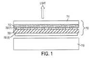
- FIG. 1illustrates schematically a cross-section of an exemplary position sensing panel
- FIG. 2illustrates schematically the arrangement of driving and sensing electrodes of an exemplary position sensing panel
- FIG. 3illustrates schematically the sensing electrodes of FIG. 2 ;
- FIG. 4illustrates schematically the drive electrodes for use in an exemplary position-sensing panel
- FIG. 5illustrates an arrangement of drive electrodes of FIG. 4 and sensing electrodes of an exemplary position sensing panel.
- a displaymay be overlaid with a position-sensing panel.
- the displaymay include various forms. Examples include, but are not limited to a liquid crystal (for example, active matrix liquid crystal), electroluminescent, electrophoretic, plasma, cathode-ray display, OLED, or the like. It will be appreciated that light emitted from the display must be able to pass through the position sensing panel with minimal absorption or obstruction in order to be clearly visible.
- FIG. 1illustrates an exemplary touch position-sensing panel 700 which overlies a display 710 .
- a substrate 703has a first 705 (X) and second 705 (Y) electrodes provided on opposite sides of the substrate 703 .
- the substrate 703has a surface on each side.
- the electrodes 705 (X) and 705 (Y)may be formed on opposing surfaces of the substrate 703 .
- the substrate 703is also provided adjacent to the display 710 such that one electrode 705 (X) is between the display 710 and the substrate 703 .
- An air gapis formed between the display 710 and the first electrode 705 (X) and an adhesive layer 712 is between the second electrode 705 (Y) and the transparent covering sheet 711 .
- the touch position-sensing panelmay have a second substrate (not shown).
- a touch position-sensing panelhas a transparent panel, a first adhesive layer on the panel, a first electrode layer comprising first electrodes, a first substrate, a second adhesive layer, a second electrode layer comprising second electrodes, and a second substrate.
- the first conductive electrode layeris attached to the first substrate and the second electrode is attached to the second substrate.
- Display 710may be selected from any of the aforementioned displays.
- Substrate 703which forms a core of the position-sensing panel 700 is formed from a transparent, non-conductive material such as glass or a plastic.
- suitable plastic substrate materialsinclude, but are not limited to Polyethylene terephthalate (PET), Polyethylene Naphthalate (PEN), or polycarbonate (PC).
- PETPolyethylene terephthalate
- PENPolyethylene Naphthalate
- PCpolycarbonate
- the panel structure and production methodologymay be utilized in other types of touch position sensing panels.
- drive (X) electrodes 705 (X)are provided on one surface of the substrate 703
- sensing (Y) electrodes 705 (Y)are provided on the opposing surface of the substrate 703 .
- Capacitive sensing channelsare formed at the capacitive coupling nodes which exist in the localized regions surrounding where the first and second electrodes 705 (X) and 705 (Y) cross over each other (separated by the non-conductive substrate 70
- Transparent covering sheet 711is provided over the substrate 703 , and may be joined thereto by any means.
- One exemplary meansis a pressure-sensitive adhesive.
- the covering sheet 711may be glass, polycarbonate, or PMMA.
- ITOis discussed here by way of an example of a clear conductive material for a set of the electrodes, e.g. for the drive electrodes 705 (X) in FIG. 1 .
- any clear conductive materialmay be used, such as other inorganic and organic conductive materials, such as ATO (Antimony tin oxide), tin oxide, PEDOT or other conductive polymers, carbon nanotube or metal nanowire impregnated materials, and the like.
- the drive electrodes 705 (X)have solid areas of ITO (in this example, ITO stripes, shown as outlines), and the sensing electrodes 705 (Y) are formed in fine line patterns, described in more detail below.
- Sensing area 720 of the position sensing paneldenoted by the dotted line in FIG. 2 , encompasses each or substantially each of the intersections 730 formed by the X and Y electrodes.
- the gaps between adjacent X electrode barsare made as narrow as possible to enhance their shielding ability against noise arising from the underlying display.
- at least 90% of the sensing area 720is covered by ITO, and the gap between adjacent ITO X electrodes is preferably no more than 200 microns. Substantially the whole of the area of each intersection 730 is shielded by the solid drive electrode bars.
- the ITO barsform drive electrodes in which each bar forms a plurality of channels with sensing electrodes on an adjacent plane.
- the shape of the drive electrodes and the interconnection between the channels of any given electrodemay be modified, for example according to the type of touch with which the position sensing panel is intended to be used.
- the stripesmay have saw-tooth or diamond shape edges (and therefore attendant inter-stripe gaps) to facilitate field interpolation to aid in smoothing positional response (not shown).
- the drive electrodeshave a width of from about 3 mm to about 12 mm depending on design.
- the sensing electrodes 705 (Y)are formed from a conductive material, such as a metal. Suitable metals include copper, silver, gold, aluminum, and tin and other metals suitable for use in conductive wiring.
- the sensing electrodesare patterned in fine lines to allow most of the light emitted from the display and incident on the sensing electrode layer to pass through the sensing electrode layer.
- the fine linesare optionally no more than 20 microns wide.
- the fine linescan be 10 microns wide.
- the fine linescan be 5 microns wide.
- An exemplary rangeis 3-10 microns. Narrower lines reduce their visibility to the naked eye and are thus preferred.
- the position sensing panelmay be formed such that no more than 10%, or no more than 5%, or no more than 3% of the active area is covered by Y electrodes, thus allowing for good transparency of the position sensing panel. Moreover, at these thicknesses the fine line pattern is invisible or virtually invisible to the naked eye and as such will not result in any perceptible darkening or other loss of display quality.
- FIG. 2illustrates sensing electrodes 705 (Y) formed as outlines of stripes in a crisscross pattern although it will be appreciated that any pattern may be used that allows most light incident on the sensing electrode layer to pass through gaps in the layer.
- the number of rows and columns shownis by way of illustration only, and the number shown is not limiting.
- Drive electrode connecting lines 707are shown leading out from the drive electrodes 705 (X) for connection to a control unit (not shown).
- Sensing electrode connecting lines 708likewise are provided to connect sensing electrodes 705 (Y) to the same or a different control unit.
- the patterns of the connecting linesare shown by way of an example only.
- FIG. 3illustrates the sensing electrode layer of FIG. 2 with the sensing electrodes 705 (Y) shown in isolation from the rest of the position sensing panel.
- each sensing electrode 705 (Y)comprises a pattern, such as a rectangular perimeter line and crisscross pattern.
- the fine line patternallows most light incident on this electrode layer to pass through the gaps in the layer with minimal obstruction.
- the lines making up electrodes 705 (Y)can be arranged in an anti-moire pattern to suppress optical interference effects with the underlying display, for example by using odd angles for the lines, breaking up straight lines into zigzag patterns, using curved lines, using randomized line segment angles and placements, and the like.
- FIG. 4is a further example illustrating another arrangement of the drive electrodes.
- Sense electrodesmay be formed as in the previous examples, although they are omitted here for ease of illustration of the drive electrodes.
- the drive electrodes 705 (X)have solid areas of ITO that together cover substantially the whole of the active area of the position sensing panel, except in regions between the drive electrodes.
- a fine line pattern of conductive material, optionally fine line metalis provided in each block area in direct contact with electrode ITO. This fine line pattern forms an auxiliary conductor 709 that may serve to increase the conductivity of the drive electrode 705 (X) associated with the auxiliary conductor 709 .
- the auxiliary conductor 709allows most light incident on it to pass through.
- the thickness of the fine line pattern forming the auxiliary conductor 709optionally has a line thickness and active area coverage selected from the same range as the fine line patterns forming the sensing electrodes 705 (Y).
- the auxiliary conductor 709is patterned in a crisscross pattern similar to the pattern used to form the sensing electrodes 705 (Y); however, it will be appreciated that other patterns, including but not limited to one or more straight lines running across each electrode 705 (X), may be provided.
- the auxiliary conductors 709 of the driving electrodescan be arranged in an anti-moire pattern as discussed supra in conjunction with the 705 (Y) electrodes.
- Connecting lines 707 that connect the drive electrodes 705 (X) to a control unitmay be formed as part of the process of forming the auxiliary conductors 709 , as described in more detail below.
- FIG. 5illustrates an arrangement of driving electrodes 705 (X) having auxiliary conductors 709 as illustrated in FIG. 4 and sensing electrodes 705 (Y) as illustrated in FIG. 3 .
- the fine line patterns of the auxiliary conductors 709 and the sensing electrodes 705 (Y)are such that most light emitted from an underlying display may still pass through the position-sensing panel.
- the transparency of the position sensing paneloptionally transmits at least 95% of light having a wavelength in the visible part of the electromagnetic spectrum that is incident on the panel, in particular from a display underlying the panel.
- the process of manufacturing the position-sensing panel illustrated in FIGS. 1-4includes the steps of patterning drive electrodes, such as ITO drive electrodes, on one substrate surface and patterning fine line sensing electrodes on the opposite surface of the same substrate layer and, in the case of the example illustrated in FIGS. 4 and 5 , forming a fine-line metal pattern associated with the drive electrodes.
- patterning drive electrodessuch as ITO drive electrodes
- the process of patterning the electrodesmay include the following steps of depositing a positive or negative resist over unpatterned ITO on a substrate; exposing the photoresist to UV light through a mask of the appropriate pattern; developing the resist by washing away unexposed resist with a solvent, and then etching away the exposed ITO areas using a suitable etchant; and finally removing the exposed photoresist using a suitable solvent.
- One suitable etching liquid for use in removing exposed ITOis, for example an etching acid.
- An example of a suitable removal liquid for the photoresistincludes organic solvents.
- Other suitable positive and negative photoresists, etching liquids and photoresist removal liquidsmay also be used.
- ITOmay for example be deposited on the substrate by sputtering ITO onto the substrate using a shadow mask having a pattern suitable for formation of electrodes in the required shape as described above.
- the process of patterning the fine line Y electrodesmay include deposition of the conductive material, for example metal, by evaporation through a mask in the appropriate pattern.
- the fine-line metalmay be formed by a printing process in which a conductive material or conductive material precursor is printed (for example, by inkjet printing) to form the Y electrode pattern and, in the case where a catalytic precursor ink is used, treating the precursor ink to convert it to the final conductive material, for example by electroless plating.
- the substratemay be uniformly coated with a catalytic photosensitive ink which is exposed to UV light through a photomask or vector-exposed to UV light from a laser or other suitable light source, rinsed with solvent to wash away the unexposed ink, then immersing the remaining ink in a metal plating bath to form the fine conductive traces.
- Suitable catalytic inksare commercially available, for example, from Conductive Inkjet Technology Ltd, UK.
- Lead-outs 707 , 708 for connection of the sensing electrodes to a control unit of the position-sensing panelmay be formed in the same process step as formation of the sensing electrodes.
- Auxiliary conductorsmay be formed in the same way as the sensing electrodes.
- the same methode.g. evaporation or printing
- the fine metal conductor linesare formed first using one of the methods described supra in conjunction with the sensing lines, followed by sputtering ITO on top of the metal lines through a mask, or by printing a clear conductive organic polymer such as PEDOT on top of the lines using a suitable printing process.
- the auxiliary conductorsmay be formed with lead-outs for connection of the drive electrodes to a control unit of the position-sensing panel.
- the auxiliary conductorsare deposited before deposition of ITO, however the auxiliary conductors may alternatively be deposited after deposition of ITO, for example by any of a number of printing processes.
- the touch position sensors described abovecan be attached to numerous electronic devices, such as computers, personal digital assistants (PDA), satellite navigation devices, mobile phones, portable media players, portable game consoles, public information kiosks, point of sale systems etc. All of these electronic devices typically include a central processor or other processing device for executing program instructions, an internal communication bus, various types of memory or storage media (RAM, ROM, EEPROM, cache memory, disk drives etc.) for code and data storage, and one or more network interface cards or ports for communication purposes.
- PDApersonal digital assistants
- satellite navigation devicesmobile phones, portable media players, portable game consoles, public information kiosks, point of sale systems etc. All of these electronic devices typically include a central processor or other processing device for executing program instructions, an internal communication bus, various types of memory or storage media (RAM, ROM, EEPROM, cache memory, disk drives etc.) for code and data storage, and one or more network interface cards or ports for communication purposes.
- RAMrandom access memory
- ROMread only memory
- EEPROMelectrically erasable
- the exemplary technologies discussed in the detailed description abovemay provide a touch position sensing panel with one or more properties of: thinness, shielding of the panel by the drive electrodes from electric field noise, high transparency and low manufacturing cost.
Landscapes
- Engineering & Computer Science (AREA)
- General Engineering & Computer Science (AREA)
- Theoretical Computer Science (AREA)
- Human Computer Interaction (AREA)
- Physics & Mathematics (AREA)
- General Physics & Mathematics (AREA)
- Position Input By Displaying (AREA)
Abstract
Description
Claims (20)
Priority Applications (1)
| Application Number | Priority Date | Filing Date | Title |
|---|---|---|---|
| US12/838,165US9081427B2 (en) | 2010-07-16 | 2010-07-16 | Position-sensing panel and method |
Applications Claiming Priority (1)
| Application Number | Priority Date | Filing Date | Title |
|---|---|---|---|
| US12/838,165US9081427B2 (en) | 2010-07-16 | 2010-07-16 | Position-sensing panel and method |
Publications (2)
| Publication Number | Publication Date |
|---|---|
| US20120013544A1 US20120013544A1 (en) | 2012-01-19 |
| US9081427B2true US9081427B2 (en) | 2015-07-14 |
Family
ID=45466560
Family Applications (1)
| Application Number | Title | Priority Date | Filing Date |
|---|---|---|---|
| US12/838,165Expired - Fee RelatedUS9081427B2 (en) | 2010-07-16 | 2010-07-16 | Position-sensing panel and method |
Country Status (1)
| Country | Link |
|---|---|
| US (1) | US9081427B2 (en) |
Families Citing this family (23)
| Publication number | Priority date | Publication date | Assignee | Title |
|---|---|---|---|---|
| US20120074961A1 (en)* | 2010-09-29 | 2012-03-29 | Kopin Corporation | Capacitive sensor with active shield electrode |
| US9077344B2 (en)* | 2010-12-07 | 2015-07-07 | Atmel Corporation | Substrate for electrical component and method |
| KR20130021648A (en)* | 2011-08-23 | 2013-03-06 | 삼성전기주식회사 | Touch panel |
| TW201332782A (en)* | 2011-10-25 | 2013-08-16 | Unipixel Displays Inc | Method of manufacturing a capacative touch sensor circuit using flexographic printing |
| CN103105962B (en)* | 2011-11-09 | 2016-04-06 | 宸鸿科技(厦门)有限公司 | Contact panel, touch electrode structure and preparation method thereof |
| KR20130051803A (en)* | 2011-11-10 | 2013-05-21 | 삼성전기주식회사 | Touch panel |
| US20130155001A1 (en)* | 2011-12-19 | 2013-06-20 | Esat Yilmaz | Low-Resistance Electrodes |
| EP2620846B1 (en)* | 2012-01-27 | 2017-08-09 | BlackBerry Limited | Electronic device with capacitive touch-sensitive display |
| US9262020B2 (en) | 2012-01-27 | 2016-02-16 | Blackberry Limited | Electronic device with capacitive touch-sensitive display |
| JP5812895B2 (en)* | 2012-02-28 | 2015-11-17 | 株式会社ジャパンディスプレイ | Proximity detection device, proximity detection method, electronic device |
| US9046974B2 (en)* | 2012-02-28 | 2015-06-02 | Eastman Kodak Company | Transparent touch-screen capacitor with micro-wire electrode |
| GB2499987B (en) | 2012-03-02 | 2017-01-11 | Novalia Ltd | Touch-sensitive input device |
| GB2520793B (en)* | 2012-03-02 | 2016-11-02 | Novalia Ltd | Touch-sensitive input device |
| KR101521681B1 (en)* | 2012-04-24 | 2015-05-19 | 삼성전기주식회사 | Touch Panel |
| US9244572B2 (en)* | 2012-05-04 | 2016-01-26 | Blackberry Limited | Electronic device including touch-sensitive display and method of detecting touches |
| US9609736B2 (en)* | 2012-06-29 | 2017-03-28 | Lg Innotek Co., Ltd. | Touch panel and method of manufacturing the same |
| CN104007863A (en)* | 2013-02-26 | 2014-08-27 | 北京京东方光电科技有限公司 | Single-layer touch screen and manufacturing method thereof and touch screen displayer |
| US9436324B2 (en) | 2013-11-04 | 2016-09-06 | Blackberry Limited | Electronic device including touch-sensitive display and method of detecting touches |
| KR102189313B1 (en)* | 2013-11-28 | 2020-12-10 | 삼성디스플레이 주식회사 | Display device |
| TWM481451U (en)* | 2014-02-20 | 2014-07-01 | Hannstouch Solution Inc | Single layer solution touch panel |
| CN106062618B (en)* | 2014-02-28 | 2019-04-16 | 凸版印刷株式会社 | Liquid crystal display device |
| TW201837685A (en)* | 2017-04-14 | 2018-10-16 | 瑞鼎科技股份有限公司 | Capacitive touch panel |
| CN115657878B (en) | 2022-12-08 | 2023-04-25 | 惠科股份有限公司 | Touch array substrate, touch positioning method and display panel |
Citations (26)
| Publication number | Priority date | Publication date | Assignee | Title |
|---|---|---|---|---|
| US5565658A (en)* | 1992-07-13 | 1996-10-15 | Cirque Corporation | Capacitance-based proximity with interference rejection apparatus and methods |
| US7151528B2 (en)* | 1999-06-22 | 2006-12-19 | Cirque Corporation | System for disposing a proximity sensitive touchpad behind a mobile phone keypad |
| US20070062739A1 (en) | 2005-09-20 | 2007-03-22 | Harald Philipp | Touch Sensitive Screen |
| US20090315854A1 (en) | 2008-06-18 | 2009-12-24 | Epson Imaging Devices Corporation | Capacitance type input device and display device with input function |
| US7663607B2 (en) | 2004-05-06 | 2010-02-16 | Apple Inc. | Multipoint touchscreen |
| US20100045632A1 (en) | 2008-04-10 | 2010-02-25 | Atmel Corporation | Capacitive Position Sensor |
| US7808487B2 (en)* | 2001-06-06 | 2010-10-05 | Cirque Corporation | System for disposing a proximity sensitive touchpad behind a mobile phone keymat |
| US20100265214A1 (en)* | 2007-07-31 | 2010-10-21 | Kent Displays Incorporated | Writing tablet information recording device |
| US20100328240A1 (en)* | 2009-06-29 | 2010-12-30 | Wacom Co., Ltd. | Position detector, position detecting circuit and position detecting method |
| US20110007011A1 (en)* | 2009-07-13 | 2011-01-13 | Ocular Lcd Inc. | Capacitive touch screen with a mesh electrode |
| US7875814B2 (en) | 2005-07-21 | 2011-01-25 | Tpo Displays Corp. | Electromagnetic digitizer sensor array structure |
| US20110050605A1 (en)* | 2009-09-02 | 2011-03-03 | Mstar Semiconductor, Inc. | Touch Sensing Module, Display Apparatus and Manufacturing Method Thereof |
| US7920129B2 (en) | 2007-01-03 | 2011-04-05 | Apple Inc. | Double-sided touch-sensitive panel with shield and drive combined layer |
| US8031174B2 (en) | 2007-01-03 | 2011-10-04 | Apple Inc. | Multi-touch surface stackup arrangement |
| US8031094B2 (en) | 2009-09-11 | 2011-10-04 | Apple Inc. | Touch controller with improved analog front end |
| US8040326B2 (en) | 2007-06-13 | 2011-10-18 | Apple Inc. | Integrated in-plane switching display and touch sensor |
| US8049732B2 (en) | 2007-01-03 | 2011-11-01 | Apple Inc. | Front-end signal compensation |
| US20120098779A1 (en)* | 2009-07-01 | 2012-04-26 | Akira Nakanishi | Touch panel |
| US8179381B2 (en) | 2008-02-28 | 2012-05-15 | 3M Innovative Properties Company | Touch screen sensor |
| US20120242592A1 (en) | 2011-03-21 | 2012-09-27 | Rothkopf Fletcher R | Electronic devices with flexible displays |
| US20120242588A1 (en) | 2011-03-21 | 2012-09-27 | Myers Scott A | Electronic devices with concave displays |
| WO2012129247A2 (en) | 2011-03-21 | 2012-09-27 | Apple Inc. | Electronic devices with flexible displays |
| US20120243719A1 (en) | 2011-03-21 | 2012-09-27 | Franklin Jeremy C | Display-Based Speaker Structures for Electronic Devices |
| US20120243151A1 (en) | 2011-03-21 | 2012-09-27 | Stephen Brian Lynch | Electronic Devices With Convex Displays |
| US8368656B2 (en)* | 2008-07-04 | 2013-02-05 | Au Optronics Corp. | Electroluminescent display touch panel |
| US20130076612A1 (en) | 2011-09-26 | 2013-03-28 | Apple Inc. | Electronic device with wrap around display |
- 2010
- 2010-07-16USUS12/838,165patent/US9081427B2/ennot_activeExpired - Fee Related
Patent Citations (26)
| Publication number | Priority date | Publication date | Assignee | Title |
|---|---|---|---|---|
| US5565658A (en)* | 1992-07-13 | 1996-10-15 | Cirque Corporation | Capacitance-based proximity with interference rejection apparatus and methods |
| US7151528B2 (en)* | 1999-06-22 | 2006-12-19 | Cirque Corporation | System for disposing a proximity sensitive touchpad behind a mobile phone keypad |
| US7808487B2 (en)* | 2001-06-06 | 2010-10-05 | Cirque Corporation | System for disposing a proximity sensitive touchpad behind a mobile phone keymat |
| US7663607B2 (en) | 2004-05-06 | 2010-02-16 | Apple Inc. | Multipoint touchscreen |
| US7875814B2 (en) | 2005-07-21 | 2011-01-25 | Tpo Displays Corp. | Electromagnetic digitizer sensor array structure |
| US20070062739A1 (en) | 2005-09-20 | 2007-03-22 | Harald Philipp | Touch Sensitive Screen |
| US7920129B2 (en) | 2007-01-03 | 2011-04-05 | Apple Inc. | Double-sided touch-sensitive panel with shield and drive combined layer |
| US8031174B2 (en) | 2007-01-03 | 2011-10-04 | Apple Inc. | Multi-touch surface stackup arrangement |
| US8049732B2 (en) | 2007-01-03 | 2011-11-01 | Apple Inc. | Front-end signal compensation |
| US8040326B2 (en) | 2007-06-13 | 2011-10-18 | Apple Inc. | Integrated in-plane switching display and touch sensor |
| US20100265214A1 (en)* | 2007-07-31 | 2010-10-21 | Kent Displays Incorporated | Writing tablet information recording device |
| US8179381B2 (en) | 2008-02-28 | 2012-05-15 | 3M Innovative Properties Company | Touch screen sensor |
| US20100045632A1 (en) | 2008-04-10 | 2010-02-25 | Atmel Corporation | Capacitive Position Sensor |
| US20090315854A1 (en) | 2008-06-18 | 2009-12-24 | Epson Imaging Devices Corporation | Capacitance type input device and display device with input function |
| US8368656B2 (en)* | 2008-07-04 | 2013-02-05 | Au Optronics Corp. | Electroluminescent display touch panel |
| US20100328240A1 (en)* | 2009-06-29 | 2010-12-30 | Wacom Co., Ltd. | Position detector, position detecting circuit and position detecting method |
| US20120098779A1 (en)* | 2009-07-01 | 2012-04-26 | Akira Nakanishi | Touch panel |
| US20110007011A1 (en)* | 2009-07-13 | 2011-01-13 | Ocular Lcd Inc. | Capacitive touch screen with a mesh electrode |
| US20110050605A1 (en)* | 2009-09-02 | 2011-03-03 | Mstar Semiconductor, Inc. | Touch Sensing Module, Display Apparatus and Manufacturing Method Thereof |
| US8031094B2 (en) | 2009-09-11 | 2011-10-04 | Apple Inc. | Touch controller with improved analog front end |
| US20120242592A1 (en) | 2011-03-21 | 2012-09-27 | Rothkopf Fletcher R | Electronic devices with flexible displays |
| US20120242588A1 (en) | 2011-03-21 | 2012-09-27 | Myers Scott A | Electronic devices with concave displays |
| WO2012129247A2 (en) | 2011-03-21 | 2012-09-27 | Apple Inc. | Electronic devices with flexible displays |
| US20120243719A1 (en) | 2011-03-21 | 2012-09-27 | Franklin Jeremy C | Display-Based Speaker Structures for Electronic Devices |
| US20120243151A1 (en) | 2011-03-21 | 2012-09-27 | Stephen Brian Lynch | Electronic Devices With Convex Displays |
| US20130076612A1 (en) | 2011-09-26 | 2013-03-28 | Apple Inc. | Electronic device with wrap around display |
Non-Patent Citations (8)
| Title |
|---|
| Cambrios Technologies Corporation Awarded Department of Defense Contract for Flexible Solar Cells, Sunnyvale, CA, Apr. 12, 2010, Cambrios Technologies Corp., Printed from website: http://www.cambrios.com/200/DOD-Release.htm on Apr. 20, 2010. |
| Core Applications & Technologies, Printing of Antennas and Flexible Circuits, Conductive InkJet Technology Ltd. (2009). |
| Horteis et al., "Fine Line Printed and Plated Contacts on High Ohmic Emitters Enabling 20% Cell Efficiency," Fraunhofer Institute for Solar Energy Systems, IEEE (2009). |
| Latest News, Conductive InkJet Technology, Printed from Website: http://www.conductiveinkjet.com/about-us/latest-news/2009.aspx on Apr. 20, 2010. |
| News, New Silver Conductive Inks Target High-Growth Touch Screen and OLED Markets, DuPont Microcircuit Materials Expands Innovative Offerings for Printed Electronics, Research Triangle Park, N.C., Apr. 13, 2010, Printed from website: http://www2dupont.com/MCM/en-US/news-events/article20100413.html on Apr. 20, 2010. |
| U.S. Appl. No. 61/454,894, filed Mar. 21, 2011, Rothkopf. |
| U.S. Appl. No. 61/454,936, filed Mar. 21, 2011, Myers. |
| U.S. Appl. No. 61/454,950, filed Mar. 21, 2011, Lynch. |
Also Published As
| Publication number | Publication date |
|---|---|
| US20120013544A1 (en) | 2012-01-19 |
Similar Documents
| Publication | Publication Date | Title |
|---|---|---|
| US9081427B2 (en) | Position-sensing panel and method | |
| US8786572B2 (en) | Touch position-sensing panel and method | |
| US9252768B2 (en) | Position-sensing panel | |
| US9218561B2 (en) | Touch sensor with RFID | |
| US9465491B2 (en) | Method for forming a capacitive touch sensor for identifying a fingerprint | |
| US9442535B2 (en) | Touch sensor with integrated antenna | |
| EP2386937B1 (en) | Capacitive touch panel and method of reducing visibility of metal conductors in the same | |
| CN103168335B (en) | Soft-touch control | |
| EP2737390B1 (en) | Capacitive touch panel and a method of manufacturing the same | |
| JP5942454B2 (en) | Touch panel sensor, display device with touch panel, and method of manufacturing touch panel sensor | |
| US20230376159A1 (en) | Touch substrate, method for manufacturing touch substrate and display apparatus | |
| US20140333555A1 (en) | Touch sensor and electronic device having the same | |
| KR101521681B1 (en) | Touch Panel | |
| US20120242585A1 (en) | Position sensing panel | |
| CN213904304U (en) | Touch substrate and display device | |
| US9626045B1 (en) | Position-sensing panel and related methods | |
| JP6138059B2 (en) | Touch panel | |
| US20120127079A1 (en) | Electrode interconnect | |
| KR101886279B1 (en) | Fabrication method of electrode-pattern of touch panel | |
| JP2015225654A (en) | Touch sensor | |
| JP2015032214A (en) | Display device with touch panel sensor and touch position detection function | |
| US20170199599A1 (en) | Capacitive touch panel | |
| US10306758B2 (en) | Enhanced conductors | |
| KR20140133413A (en) | Touch Sensor and Electronic Device having the same | |
| JP2011186977A (en) | Manufacturing method of input device |
Legal Events
| Date | Code | Title | Description |
|---|---|---|---|
| AS | Assignment | Owner name:QRG LIMITED, UNITED KINGDOM Free format text:ASSIGNMENT OF ASSIGNORS INTEREST;ASSIGNOR:PHILIPP, HARALD;REEL/FRAME:025082/0672 Effective date:20100717 Owner name:ATMEL CORPORATION, CALIFORNIA Free format text:ASSIGNMENT OF ASSIGNORS INTEREST;ASSIGNOR:QRG LIMITED;REEL/FRAME:025082/0675 Effective date:20100723 | |
| AS | Assignment | Owner name:MORGAN STANLEY SENIOR FUNDING, INC. AS ADMINISTRATIVE AGENT, NEW YORK Free format text:PATENT SECURITY AGREEMENT;ASSIGNOR:ATMEL CORPORATION;REEL/FRAME:031912/0173 Effective date:20131206 Owner name:MORGAN STANLEY SENIOR FUNDING, INC. AS ADMINISTRAT Free format text:PATENT SECURITY AGREEMENT;ASSIGNOR:ATMEL CORPORATION;REEL/FRAME:031912/0173 Effective date:20131206 | |
| STCF | Information on status: patent grant | Free format text:PATENTED CASE | |
| AS | Assignment | Owner name:ATMEL CORPORATION, CALIFORNIA Free format text:TERMINATION AND RELEASE OF SECURITY INTEREST IN PATENT COLLATERAL;ASSIGNOR:MORGAN STANLEY SENIOR FUNDING, INC.;REEL/FRAME:038376/0001 Effective date:20160404 | |
| AS | Assignment | Owner name:JPMORGAN CHASE BANK, N.A., AS ADMINISTRATIVE AGENT, ILLINOIS Free format text:SECURITY INTEREST;ASSIGNOR:ATMEL CORPORATION;REEL/FRAME:041715/0747 Effective date:20170208 Owner name:JPMORGAN CHASE BANK, N.A., AS ADMINISTRATIVE AGENT Free format text:SECURITY INTEREST;ASSIGNOR:ATMEL CORPORATION;REEL/FRAME:041715/0747 Effective date:20170208 | |
| AS | Assignment | Owner name:JPMORGAN CHASE BANK, N.A., AS ADMINISTRATIVE AGENT, ILLINOIS Free format text:SECURITY INTEREST;ASSIGNORS:MICROCHIP TECHNOLOGY INCORPORATED;SILICON STORAGE TECHNOLOGY, INC.;ATMEL CORPORATION;AND OTHERS;REEL/FRAME:046426/0001 Effective date:20180529 Owner name:JPMORGAN CHASE BANK, N.A., AS ADMINISTRATIVE AGENT Free format text:SECURITY INTEREST;ASSIGNORS:MICROCHIP TECHNOLOGY INCORPORATED;SILICON STORAGE TECHNOLOGY, INC.;ATMEL CORPORATION;AND OTHERS;REEL/FRAME:046426/0001 Effective date:20180529 | |
| AS | Assignment | Owner name:WELLS FARGO BANK, NATIONAL ASSOCIATION, AS NOTES COLLATERAL AGENT, CALIFORNIA Free format text:SECURITY INTEREST;ASSIGNORS:MICROCHIP TECHNOLOGY INCORPORATED;SILICON STORAGE TECHNOLOGY, INC.;ATMEL CORPORATION;AND OTHERS;REEL/FRAME:047103/0206 Effective date:20180914 Owner name:WELLS FARGO BANK, NATIONAL ASSOCIATION, AS NOTES C Free format text:SECURITY INTEREST;ASSIGNORS:MICROCHIP TECHNOLOGY INCORPORATED;SILICON STORAGE TECHNOLOGY, INC.;ATMEL CORPORATION;AND OTHERS;REEL/FRAME:047103/0206 Effective date:20180914 | |
| MAFP | Maintenance fee payment | Free format text:PAYMENT OF MAINTENANCE FEE, 4TH YEAR, LARGE ENTITY (ORIGINAL EVENT CODE: M1551); ENTITY STATUS OF PATENT OWNER: LARGE ENTITY Year of fee payment:4 | |
| AS | Assignment | Owner name:MICROCHIP TECHNOLOGY INCORPORATED, ARIZONA Free format text:RELEASE OF SECURITY INTEREST IN CERTAIN PATENT RIGHTS;ASSIGNOR:JPMORGAN CHASE BANK, N.A., AS ADMINISTRATIVE AGENT;REEL/FRAME:047976/0884 Effective date:20181221 Owner name:ATMEL CORPORATION, ARIZONA Free format text:RELEASE OF SECURITY INTEREST IN CERTAIN PATENT RIGHTS;ASSIGNOR:WELLS FARGO BANK, NATIONAL ASSOCIATION, AS NOTES COLLATERAL AGENT;REEL/FRAME:047976/0937 Effective date:20181221 Owner name:MICROCHIP TECHNOLOGY INCORPORATED, ARIZONA Free format text:RELEASE OF SECURITY INTEREST IN CERTAIN PATENT RIGHTS;ASSIGNOR:WELLS FARGO BANK, NATIONAL ASSOCIATION, AS NOTES COLLATERAL AGENT;REEL/FRAME:047976/0937 Effective date:20181221 Owner name:ATMEL CORPORATION, ARIZONA Free format text:RELEASE OF SECURITY INTEREST IN CERTAIN PATENT RIGHTS;ASSIGNOR:JPMORGAN CHASE BANK, N.A., AS ADMINISTRATIVE AGENT;REEL/FRAME:047976/0884 Effective date:20181221 | |
| AS | Assignment | Owner name:NEODRON LIMITED, IRELAND Free format text:ASSIGNMENT OF ASSIGNORS INTEREST;ASSIGNORS:MICROCHIP TECHNOLOGY INC.;ATMEL CORPORATION;MICROCHIP TECHNOLOGY GERMANY GMBH;REEL/FRAME:048259/0840 Effective date:20181221 | |
| AS | Assignment | Owner name:MICROSEMI STORAGE SOLUTIONS, INC., ARIZONA Free format text:RELEASE BY SECURED PARTY;ASSIGNOR:JPMORGAN CHASE BANK, N.A., AS ADMINISTRATIVE AGENT;REEL/FRAME:059333/0222 Effective date:20220218 Owner name:MICROSEMI CORPORATION, ARIZONA Free format text:RELEASE BY SECURED PARTY;ASSIGNOR:JPMORGAN CHASE BANK, N.A., AS ADMINISTRATIVE AGENT;REEL/FRAME:059333/0222 Effective date:20220218 Owner name:ATMEL CORPORATION, ARIZONA Free format text:RELEASE BY SECURED PARTY;ASSIGNOR:JPMORGAN CHASE BANK, N.A., AS ADMINISTRATIVE AGENT;REEL/FRAME:059333/0222 Effective date:20220218 Owner name:SILICON STORAGE TECHNOLOGY, INC., ARIZONA Free format text:RELEASE BY SECURED PARTY;ASSIGNOR:JPMORGAN CHASE BANK, N.A., AS ADMINISTRATIVE AGENT;REEL/FRAME:059333/0222 Effective date:20220218 Owner name:MICROCHIP TECHNOLOGY INCORPORATED, ARIZONA Free format text:RELEASE BY SECURED PARTY;ASSIGNOR:JPMORGAN CHASE BANK, N.A., AS ADMINISTRATIVE AGENT;REEL/FRAME:059333/0222 Effective date:20220218 | |
| AS | Assignment | Owner name:ATMEL CORPORATION, ARIZONA Free format text:RELEASE BY SECURED PARTY;ASSIGNOR:JPMORGAN CHASE BANK, N.A., AS ADMINISTRATIVE AGENT;REEL/FRAME:059262/0105 Effective date:20220218 | |
| AS | Assignment | Owner name:MICROSEMI STORAGE SOLUTIONS, INC., ARIZONA Free format text:RELEASE BY SECURED PARTY;ASSIGNOR:WELLS FARGO BANK, NATIONAL ASSOCIATION, AS NOTES COLLATERAL AGENT;REEL/FRAME:059358/0001 Effective date:20220228 Owner name:MICROSEMI CORPORATION, ARIZONA Free format text:RELEASE BY SECURED PARTY;ASSIGNOR:WELLS FARGO BANK, NATIONAL ASSOCIATION, AS NOTES COLLATERAL AGENT;REEL/FRAME:059358/0001 Effective date:20220228 Owner name:ATMEL CORPORATION, ARIZONA Free format text:RELEASE BY SECURED PARTY;ASSIGNOR:WELLS FARGO BANK, NATIONAL ASSOCIATION, AS NOTES COLLATERAL AGENT;REEL/FRAME:059358/0001 Effective date:20220228 Owner name:SILICON STORAGE TECHNOLOGY, INC., ARIZONA Free format text:RELEASE BY SECURED PARTY;ASSIGNOR:WELLS FARGO BANK, NATIONAL ASSOCIATION, AS NOTES COLLATERAL AGENT;REEL/FRAME:059358/0001 Effective date:20220228 Owner name:MICROCHIP TECHNOLOGY INCORPORATED, ARIZONA Free format text:RELEASE BY SECURED PARTY;ASSIGNOR:WELLS FARGO BANK, NATIONAL ASSOCIATION, AS NOTES COLLATERAL AGENT;REEL/FRAME:059358/0001 Effective date:20220228 | |
| FEPP | Fee payment procedure | Free format text:MAINTENANCE FEE REMINDER MAILED (ORIGINAL EVENT CODE: REM.); ENTITY STATUS OF PATENT OWNER: LARGE ENTITY | |
| LAPS | Lapse for failure to pay maintenance fees | Free format text:PATENT EXPIRED FOR FAILURE TO PAY MAINTENANCE FEES (ORIGINAL EVENT CODE: EXP.); ENTITY STATUS OF PATENT OWNER: LARGE ENTITY | |
| STCH | Information on status: patent discontinuation | Free format text:PATENT EXPIRED DUE TO NONPAYMENT OF MAINTENANCE FEES UNDER 37 CFR 1.362 | |
| FP | Lapsed due to failure to pay maintenance fee | Effective date:20230714 |