US9081299B2 - Lithographic apparatus and device manufacturing method involving removal of liquid entering a gap - Google Patents
Lithographic apparatus and device manufacturing method involving removal of liquid entering a gapDownload PDFInfo
- Publication number
- US9081299B2 US9081299B2US13/195,248US201113195248AUS9081299B2US 9081299 B2US9081299 B2US 9081299B2US 201113195248 AUS201113195248 AUS 201113195248AUS 9081299 B2US9081299 B2US 9081299B2
- Authority
- US
- United States
- Prior art keywords
- substrate
- liquid
- projection system
- gap
- radiation
- Prior art date
- Legal status (The legal status is an assumption and is not a legal conclusion. Google has not performed a legal analysis and makes no representation as to the accuracy of the status listed.)
- Expired - Fee Related, expires
Links
Images


Classifications
- G—PHYSICS
- G03—PHOTOGRAPHY; CINEMATOGRAPHY; ANALOGOUS TECHNIQUES USING WAVES OTHER THAN OPTICAL WAVES; ELECTROGRAPHY; HOLOGRAPHY
- G03F—PHOTOMECHANICAL PRODUCTION OF TEXTURED OR PATTERNED SURFACES, e.g. FOR PRINTING, FOR PROCESSING OF SEMICONDUCTOR DEVICES; MATERIALS THEREFOR; ORIGINALS THEREFOR; APPARATUS SPECIALLY ADAPTED THEREFOR
- G03F7/00—Photomechanical, e.g. photolithographic, production of textured or patterned surfaces, e.g. printing surfaces; Materials therefor, e.g. comprising photoresists; Apparatus specially adapted therefor
- G03F7/70—Microphotolithographic exposure; Apparatus therefor
- G03F7/70058—Mask illumination systems
- G03F7/70141—Illumination system adjustment, e.g. adjustments during exposure or alignment during assembly of illumination system
- G—PHYSICS
- G03—PHOTOGRAPHY; CINEMATOGRAPHY; ANALOGOUS TECHNIQUES USING WAVES OTHER THAN OPTICAL WAVES; ELECTROGRAPHY; HOLOGRAPHY
- G03F—PHOTOMECHANICAL PRODUCTION OF TEXTURED OR PATTERNED SURFACES, e.g. FOR PRINTING, FOR PROCESSING OF SEMICONDUCTOR DEVICES; MATERIALS THEREFOR; ORIGINALS THEREFOR; APPARATUS SPECIALLY ADAPTED THEREFOR
- G03F7/00—Photomechanical, e.g. photolithographic, production of textured or patterned surfaces, e.g. printing surfaces; Materials therefor, e.g. comprising photoresists; Apparatus specially adapted therefor
- G03F7/20—Exposure; Apparatus therefor
- G—PHYSICS
- G03—PHOTOGRAPHY; CINEMATOGRAPHY; ANALOGOUS TECHNIQUES USING WAVES OTHER THAN OPTICAL WAVES; ELECTROGRAPHY; HOLOGRAPHY
- G03F—PHOTOMECHANICAL PRODUCTION OF TEXTURED OR PATTERNED SURFACES, e.g. FOR PRINTING, FOR PROCESSING OF SEMICONDUCTOR DEVICES; MATERIALS THEREFOR; ORIGINALS THEREFOR; APPARATUS SPECIALLY ADAPTED THEREFOR
- G03F7/00—Photomechanical, e.g. photolithographic, production of textured or patterned surfaces, e.g. printing surfaces; Materials therefor, e.g. comprising photoresists; Apparatus specially adapted therefor
- G03F7/70—Microphotolithographic exposure; Apparatus therefor
- G03F7/70216—Mask projection systems
- G03F7/70341—Details of immersion lithography aspects, e.g. exposure media or control of immersion liquid supply
- G—PHYSICS
- G03—PHOTOGRAPHY; CINEMATOGRAPHY; ANALOGOUS TECHNIQUES USING WAVES OTHER THAN OPTICAL WAVES; ELECTROGRAPHY; HOLOGRAPHY
- G03F—PHOTOMECHANICAL PRODUCTION OF TEXTURED OR PATTERNED SURFACES, e.g. FOR PRINTING, FOR PROCESSING OF SEMICONDUCTOR DEVICES; MATERIALS THEREFOR; ORIGINALS THEREFOR; APPARATUS SPECIALLY ADAPTED THEREFOR
- G03F7/00—Photomechanical, e.g. photolithographic, production of textured or patterned surfaces, e.g. printing surfaces; Materials therefor, e.g. comprising photoresists; Apparatus specially adapted therefor
- G03F7/70—Microphotolithographic exposure; Apparatus therefor
- G03F7/708—Construction of apparatus, e.g. environment aspects, hygiene aspects or materials
- G03F7/7085—Detection arrangement, e.g. detectors of apparatus alignment possibly mounted on wafers, exposure dose, photo-cleaning flux, stray light, thermal load
- G—PHYSICS
- G03—PHOTOGRAPHY; CINEMATOGRAPHY; ANALOGOUS TECHNIQUES USING WAVES OTHER THAN OPTICAL WAVES; ELECTROGRAPHY; HOLOGRAPHY
- G03F—PHOTOMECHANICAL PRODUCTION OF TEXTURED OR PATTERNED SURFACES, e.g. FOR PRINTING, FOR PROCESSING OF SEMICONDUCTOR DEVICES; MATERIALS THEREFOR; ORIGINALS THEREFOR; APPARATUS SPECIALLY ADAPTED THEREFOR
- G03F7/00—Photomechanical, e.g. photolithographic, production of textured or patterned surfaces, e.g. printing surfaces; Materials therefor, e.g. comprising photoresists; Apparatus specially adapted therefor
- G03F7/70—Microphotolithographic exposure; Apparatus therefor
- G03F7/708—Construction of apparatus, e.g. environment aspects, hygiene aspects or materials
- G03F7/70858—Environment aspects, e.g. pressure of beam-path gas, temperature
- G03F7/70883—Environment aspects, e.g. pressure of beam-path gas, temperature of optical system
Definitions
- the present inventionrelates to a lithographic projection apparatus and a device manufacturing method.
- patterning deviceas here employed should be broadly interpreted as referring to any device that can be used to endow an incoming radiation beam with a patterned cross-section, corresponding to a pattern that is to be created in a target portion of the substrate; the term “light valve” can also be used in this context.
- the patternwill correspond to a particular functional layer in a device being created in the target portion, such as an integrated circuit or other device (see below). Examples of such a patterning device include:
- a maskThe concept of a mask is well known in lithography, and it includes mask types such as binary, alternating phase-shift, and attenuated phase-shift, as well as various hybrid mask types. Placement of such a mask in the radiation beam causes selective transmission (in the case of a transmissive mask) or reflection (in the case of a reflective mask) of the radiation impinging on the mask, according to the pattern on the mask.
- the support structurewill generally be a mask table, which ensures that the mask can be held at a desired position in the incoming radiation beam, and that it can be moved relative to the beam if so desired.
- a programmable mirror arrayis a matrix-addressable surface having a viscoelastic control layer and a reflective surface.
- the basic principle behind such an apparatusis that (for example) addressed areas of the reflective surface reflect incident light as diffracted light, whereas unaddressed areas reflect incident light as undiffracted light.
- the undiffracted lightcan be filtered out of the reflected beam, leaving only the diffracted light behind; in this manner, the beam becomes patterned according to the addressing pattern of the matrix-addressable surface.
- An alternative embodiment of a programmable mirror arrayemploys a matrix arrangement of tiny mirrors, each of which can be individually tilted about an axis by applying a suitable localized electric field, or by employing piezoelectric actuation means.
- the mirrorsare matrix-addressable, such that addressed mirrors will reflect an incoming radiation beam in a different direction to unaddressed mirrors; in this manner, the reflected beam is patterned according to the addressing pattern of the matrix-addressable mirrors.
- the matrix addressingcan be performed using suitable electronics.
- the patterning devicecan comprise one or more programmable mirror arrays. More information on mirror arrays as here referred to can be gleaned, for example, from U.S. Pat.
- the support structuremay be embodied as a frame or table, for example, which may be fixed or movable as required.
- a programmable LCD arrayAn example of such a construction is given in U.S. Pat. No. 5,229,872, which is incorporated herein by reference.
- the support structure in this casemay be embodied as a frame or table, for example, which may be fixed or movable as required.
- Lithographic projection apparatuscan be used, for example, in the manufacture of integrated circuits (ICs).
- the patterning devicemay generate a circuit pattern corresponding to an individual layer of the IC, and this pattern can be imaged onto a target portion (e.g. comprising one or more dies) on a substrate (silicon wafer) that has been coated with a layer of radiation-sensitive material (resist).
- a target portione.g. comprising one or more dies
- a substratesilicon wafer
- a layer of radiation-sensitive materialresist
- a single waferwill contain a whole network of adjacent target portions that are successively irradiated via the projection system, one at a time.
- employing patterning by a mask on a mask tablea distinction can be made between two different types of machine.
- each target portionis irradiated by exposing the entire mask pattern onto the target portion at one time; such an apparatus is commonly referred to as a stepper.
- a step-and-scan apparatuseach target portion is irradiated by progressively scanning the mask pattern under the projection beam in a given reference direction (the “scanning” direction) while synchronously scanning the substrate table parallel or anti-parallel to this direction; since, in general, the projection system will have a magnification factor M (generally ⁇ 1), the speed V at which the substrate table is scanned will be a factor M times that at which the mask table is scanned.
- Mmagnification factor
- a pattern(e.g. in a mask) is imaged onto a substrate that is at least partially covered by a layer of radiation-sensitive material (resist).
- the substratePrior to this imaging step, the substrate may undergo various procedures, such as priming, resist coating and a soft bake. After exposure, the substrate may be subjected to other procedures, such as a post-exposure bake (PEB), development, a hard bake and measurement/inspection of the imaged features.
- PEBpost-exposure bake
- This array of proceduresis used as a basis to pattern an individual layer of a device, e.g. an IC.
- Such a patterned layermay then undergo various processes such as etching, ion-implantation (doping), metallization, oxidation, chemo-mechanical polishing, etc., all intended to finish off an individual layer. If several layers are required, then the whole procedure, or a variant thereof, will have to be repeated for each new layer. Eventually, an array of devices will be present on the substrate (wafer). These devices are then separated from one another by a technique such as dicing or sawing, whence the individual devices can be mounted on a carrier, connected to pins, etc.
- the projection systemmay hereinafter be referred to as the “projection lens”; however, this term should be broadly interpreted as encompassing various types of projection system, including refractive optics, reflective optics, and catadioptric systems, for example.
- the radiation systemmay also include components operating according to any of these design types for directing, shaping or controlling the projection beam of radiation, and such components may be referred to below, collectively or singularly, as a “lens”.
- the lithographic apparatusmay be of a type having two or more substrate tables (and/or two or more mask tables). In such “multiple stage” devices the additional tables may be used in parallel, or preparatory steps may be carried out on one or more tables while one or more other tables are being used for exposures. Dual stage lithographic apparatus are described, for example, in U.S. Pat. No. 5,969,441 and PCT patent application publication WO 98/40791, incorporated herein by reference.
- liquid supply systemto provide liquid on only a localized area of the substrate and in between the final element of the projection system and the substrate (the substrate generally has a larger surface area than the final element of the projection system).
- the substrategenerally has a larger surface area than the final element of the projection system.
- liquidis supplied by at least one inlet IN onto the substrate, preferably along the direction of movement of the substrate relative to the final element, and is removed by at least one outlet OUT after having passed under the projection system. That is, as the substrate is scanned beneath the element in a ⁇ X direction, liquid is supplied at the +X side of the element and taken up at the ⁇ X side.
- FIG. 15shows the arrangement schematically in which liquid is supplied via inlet IN and is taken up on the other side of the element by outlet OUT which is connected to a low pressure source.
- the liquidis supplied along the direction of movement of the substrate relative to the final element, though this does not need to be the case.
- FIG. 23shows the arrangement schematically in which liquid is supplied via inlet IN and is taken up on the other side of the element by outlet OUT which is connected to a low pressure source.
- the liquidis supplied along the direction of movement of the substrate relative to the final element, though this does not need to be the case.
- FIG. 23shows four sets of an inlet with an outlet on either side in a regular pattern around the final element.
- a lithographic projection apparatuscomprising:
- an illuminatoradapted to condition a beam of radiation
- a support structureconfigured to hold a patterning device, the patterning device configured to pattern the beam of radiation according to a desired pattern
- a substrate tableconfigured to hold a substrate
- a projection systemadapted to project the patterned beam onto a target portion of the substrate
- a liquid supply systemconfigured to at least partly fill a space between the projection system and an object on the substrate table, with a liquid
- a sensorcapable of being positioned to be illuminated by the beam of radiation once it has passed through the liquid.
- An example sensorincludes an alignment sensor configured to align the substrate table relative to the projection system, a transmission image sensor, a focus sensor, a spot or dose sensor, an integrated lens interferometer and scanner sensor and even an alignment mark.
- the measurement gratings of the sensormay have a pitch than less than 500 nm, such pitch possibly improving the resolution of the alignment sensor.
- a device manufacturing methodcomprising:
- radiationand “beam” are used to encompass all types of electromagnetic radiation, including ultraviolet radiation (e.g. with a wavelength of 365, 248, 193, 157 or 126 nm).
- FIG. 1depicts a lithographic projection apparatus according to an embodiment of the invention
- FIG. 2depicts the liquid reservoir of a first embodiment of the invention
- FIG. 3illustrates a second embodiment of the invention
- FIG. 4illustrates an alternative form of the second embodiment of the present invention
- FIG. 5illustrates a detail of the second embodiment of the present invention
- FIG. 6 aillustrates a first version of a third embodiment of the present invention
- FIG. 6 billustrates a second version of the third embodiment
- FIG. 6 cillustrates a third version of the third embodiment
- FIG. 7illustrates in detail further aspects of the first version of the third embodiment of the present invention.
- FIG. 8illustrates a fourth embodiment of the present invention
- FIG. 9illustrates an fifth embodiment of the present invention.
- FIG. 10illustrates a sixth embodiment of the present invention
- FIG. 11illustrates a seventh embodiment of the present invention
- FIG. 12illustrates an eighth embodiment of the present invention
- FIG. 13illustrates a eighth embodiment of the present invention
- FIG. 14illustrates an alternative liquid supply system according to an embodiment of the invention
- FIG. 15illustrates, in plan, the system of FIG. 14 ;
- FIG. 16depicts an ILIAS sensor module
- FIG. 17depicts an ILIAS sensor module with an elongated transmissive plate according to an embodiment of the present invention
- FIG. 18depicts an ILIAS sensor module with a filler sheet according to an embodiment of the present invention.
- FIGS. 19 a and 19 bdepict a luminescence based DUV transmission image sensor.
- FIG. 1schematically depicts a lithographic projection apparatus according to a particular embodiment of the invention.
- the apparatuscomprises:
- the apparatusis of a transmissive type (e.g. has a transmissive mask). However, in general, it may also be of a reflective type, for example (e.g. with a reflective mask). Alternatively, the apparatus may employ another kind of patterning device, such as a programmable mirror array of a type as referred to above.
- the source LA(e.g. an excimer laser) produces a beam of radiation.
- This beamis fed into an illumination system (illuminator) IL, either directly or after having traversed conditioning means, such as a beam expander Ex, for example.
- the illuminator ILmay comprise adjusting means AM for setting the outer and/or inner radial extent (commonly referred to as ⁇ -outer and ⁇ -inner, respectively) of the intensity distribution in the beam.
- ⁇ -outer and ⁇ -innercommonly referred to as ⁇ -outer and ⁇ -inner, respectively
- itwill generally comprise various other components, such as an integrator IN and a condenser CO.
- the beam PB impinging on the mask MAhas a desired uniformity and intensity distribution in its cross-section.
- the source LAmay be within the housing of the lithographic projection apparatus (as is often the case when the source LA is a mercury lamp, for example), but that it may also be remote from the lithographic projection apparatus, the radiation beam which it produces being led into the apparatus (e.g. with the aid of suitable directing mirrors); this latter scenario is often the case when the source LA is an excimer laser.
- the current invention and claimsencompass at least both of these scenarios.
- the beam PBsubsequently intercepts the mask MA, which is held on a mask table MT. Having traversed the mask MA, the beam PB passes through the projection system PL, which focuses the beam PB onto a target portion C of the substrate W. With the aid of the second positioning device (and interferometric measuring device IF), the substrate table WT can be moved accurately, e.g. so as to position different target portions C in the path of the beam PB. Similarly, the first positioning device can be used to accurately position the mask MA with respect to the path of the beam PB, e.g. after mechanical retrieval of the mask MA from a mask library, or during a scan.
- the mask table MTmay just be connected to a short stroke actuator, or may be fixed.
- the depicted apparatuscan be used in two different modes:
- step modethe mask table MT is kept essentially stationary, and an entire mask image is projected at one time (i.e. a single “flash”) onto a target portion C.
- the substrate table WTis then shifted in the X and/or Y directions so that a different target portion C can be irradiated by the beam PB;
- Mmagnification of the projection system PL
- FIG. 2shows a liquid reservoir 10 between the projection system PL and the substrate W which is positioned on the substrate stage WT.
- the liquid reservoir 10is filled with a liquid 11 having a relatively high refractive index, e.g. water or a suspension of particles in water, provided via inlet/outlet ducts 13 .
- the liquidhas the effect that the radiation of the projection beam is a shorter wavelength in the liquid than in gas (e.g., air) or in a vacuum, allowing smaller features to be resolved.
- gase.g., air
- the resolution limit of a projection systemis determined, inter alia, by the wavelength of the projection beam and the numerical aperture of the system.
- the presence of the liquidmay also be regarded as increasing the effective numerical aperture.
- the liquidis effective to increase the depth of field.
- the reservoir 10forms, in an embodiment, a contactless seal to the substrate W around the image field of the projection system PL so that the liquid is confined to fill the space between the substrate's primary surface, which faces the projection system PL, and the final optical element of the projection system PL.
- the reservoiris formed by a seal member 12 positioned below and surrounding the final element of the projection system PL.
- the liquid supply systemprovides liquid on only a localized area of the substrate.
- the seal member 12forms part of the liquid supply system for filling the space between the final element of the projection system and the substrate with a liquid. This liquid is brought into the space below the projection system and within the seal member 12 .
- the seal member 12extends a little above the bottom element of the projection system and the liquid rises above the final element so that a buffer of liquid is provided.
- the seal member 12has an inner periphery that at the upper end closely conforms to the shape of the projection system or the final elements thereof and may, e.g. be round. At the bottom the inner periphery closely conforms to the shape of the image field, e.g. rectangular, though this is not necessarily so.
- the seal memberis substantially stationary in the XY plane relative to the projection system though there may be some relative movement in the Z direction (in the direction of the optical axis).
- a sealis formed between the seal member and the surface of the substrate. In an implementation, this seal is a contactless seal and may be a gas seal.
- the liquid 11is confined in the reservoir 10 by a seal device 16 .
- the seal deviceis a contactless seal i.e. a gas seal.
- the gas sealis formed by gas, e.g. air or synthetic air, provided under pressure via inlet 15 to the gap between seal member 12 and substrate W and extracted by first outlet 14 .
- the over pressure on the gas inlet 15 , vacuum level or under pressure on the first outlet 14 and the geometry of the gapare arranged so that there is a high-velocity gas flow inwards towards the optical axis of the apparatus that confines the liquid 11 .
- some liquidis likely to escape, for example up the first outlet 14 .
- FIGS. 14 and 15also depict a liquid reservoir defined by inlet(s) IN, outlet(s) OUT, the substrate W and the final element of projection system PL.
- the liquid supply system illustrated in FIGS. 14 and 15comprising inlet(s) IN and outlet(s) OUT, supplies liquid to the primary surface of the substrate in a localized area between the final element of the projection system and the substrate and can suffer from loss of liquid at the substrate edge.
- the liquid supply systemcan comprise that as described in relation to FIG. 2 and FIGS. 14 and 15 .
- FIGS. 3 to 5A second embodiment is illustrated in FIGS. 3 to 5 and is the same or similar as the first embodiment except as described below.
- an edge liquid supply systemprovides liquid to a reservoir 30 via a port 40 .
- the liquid in the reservoir 30is optionally the same as the immersion liquid in the liquid supply system.
- the reservoir 30is positioned on the opposite side of the substrate W to the projection system PL and adjacent the edge of the substrate W and the edge of the edge seal member 17 , 117 .
- the edge seal member 17is comprised of an element which is separate to the substrate table WT whereas in FIG. 3 the edge seal member 117 is provided by an integral portion of the substrate table WT.
- the substrate Wis supported on the substrate table WT by a so-called pimple table 20 .
- the pimple table 20comprises a plurality of projections on which the substrate W rests.
- the substrate Wis held in place by, e.g., a vacuum source sucking the substrate onto the top surface of the substrate table WT.
- a vacuum sourcesucking the substrate onto the top surface of the substrate table WT.
- the mechanism 170 shown in FIG. 4 for moving the edge seal member 17 relative to the remainder of the substrate table WTis illustrated in detail in FIG. 5 .
- the reason for moving the edge seal member 17 in this wayis so that its primary surface can be made to be substantially co-planar with the primary surface of the substrate W. This allows a smooth movement of the liquid supply system over edge portions of the substrate W so that the bottom inner periphery of the liquid supply system can be moved to positions partly on the primary surface of substrate W and partly on the primary surface of the edge seal member 17 .
- a level sensor(not illustrated) is used to detect the relative heights of the primary surfaces of the substrate W and the edge seal member 17 . Based on the results of the level sensor, control signals are sent to the actuator 171 in order to adjust the height of the primary surface of the edge seal member 17 .
- a closed loop actuatorcould also be used for this purpose.
- the actuator 171is a rotating motor which rotates a shaft 176 .
- the shaft 176is connected to a circular disc at the end distal to the motor 171 .
- the shaft 176is connected away from the centre of the disc.
- the discis located in a circular recess in a wedge portion 172 .
- Ball bearingsmay be used to reduce the amount of friction between the circular disc and the sides of the recess in the wedge portion 172 .
- the motor 171is held in place by leaf springs 177 .
- On actuation of the motorthe wedge portion is driven to the left and right as illustrated (i.e. in the direction of the slope of the wedge portion) because of the excentre position of the shaft 176 in the disc.
- the motoris prevented from moving in the same direction as the direction of movement of the wedge portion 172 by the springs 177 .
- the wedge portion 172moves left and right as illustrated in FIG. 5 , its top surface 175 (which is the surface of the wedge which is sloped in relation to the primary surface of the edge seal member 17 ) contacts the bottom sloped surface of a further wedge member 173 which is fixed to the bottom of the edge seal member 17 .
- the edge seal member 17is prevented from moving in the direction of movement of the wedge member 172 so that when the wedge member 172 moves left and right the edge seal member 17 is lowered and raised respectively. Some biasing of the edge seal member 17 towards the substrate table WT may be necessary.
- the further wedge member 173could be replaced by an alternative shape, for example a rod positioned perpendicularly to the direction of movement of the wedge 172 . If the coefficient of friction between the wedge member 172 and the further wedge member 173 is greater than the tangent of the wedge angle then the actuator 170 is self-braking meaning that no force may be needed on the wedge member 172 to hold it in place. This is advantageous as the system will then be stable when the actuator 171 is not actuated. The accuracy of the mechanism 170 is of the order of a few ⁇ m.
- a mechanismmay be provided to adjust the height of the substrate W or the member supporting the substrate W so that the primary surfaces of the edge seal member 17 , 117 and the substrate can be made substantially co-planar.
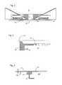
- FIGS. 6 and 7A third embodiment is illustrated in FIGS. 6 and 7 and is the same or similar as the first embodiment except as described below.
- This embodimentis described in relation to an edge seal member 117 which is an integral part of the substrate table WT. However, this embodiment is equally applicable to an edge seal member 17 which is movable relative to the substrate table WT.
- a further edge seal member 500is used to bridge the gap between the edge seal member 117 and the substrate W.
- the further edge seal memberis affixed to the edge seal member 117 .
- the further edge seal member 500is removably attachable against the surface of the substrate W opposite the primary surface.
- the further edge seal member 500can be a flexible edge seal member which is actuatable to contact the under surface of the substrate W. When the flexible edge seal member 500 is deactivated it falls away from the substrate under gravity. The way this is achieved is illustrated in FIG. 7 and is described below.
- a port 46 connected to a low pressure sourcemay be provided under the substrate W adjacent edges of the edge seal member 117 and the substrate W in some or all of the versions of this embodiment.
- the design of the area under the substratecould be the same as that of the second embodiment.
- the same systemcan be used for sensors such as a transmission image sensor (TIS) on the substrate table as opposed for the substrate W.
- TIStransmission image sensor
- the further edge seal member 500can be permanently attached to the sensor, for example using glue.
- the further edge seal member 500can be arranged to engage with the top surface of the object (that surface closest to the projection system) rather than the bottom surface. Also, the further edge seal member 500 may be provided attached to or near the top surface of the edge seal member 117 as opposed to under the edge seal member 117 as is illustrated in FIG. 6 a.
- FIG. 6 bA second version of this embodiment is illustrated in FIG. 6 b .
- Two further edge seal members 500 a , 500 bare used.
- the first of these edge seal members 500 ais the same as in the first version.
- the second of these edge seal members 500 bis affixed to the substrate table 20 i.e. underneath the substrate W and extends with its free end radially outwardly from its attachment point.
- the second further edge seal member 500 bclamps the first further edge seal member 500 a against the substrate W.
- Compressed gascan be used to deform or move the second further edge seal member 500 b.
- FIG. 6 cA third version of this embodiment is shown in FIG. 6 c .
- the third versionis the same as the second version except the first further edge seal member 500 c clamps the second further edge seal member 500 d to the substrate W. This avoids, for example, the need for the compressed gas of the second version.
- a channel 510is formed in the elongate direction of a flexible further edge seal member 500 (which, in an implementation, is an annular ring) and (a) discrete port(s) are provided in an upper surface of the flexible further edge seal member which faces the projection system PL and the underside of the substrate W.
- a vacuum source 515By connecting a vacuum source 515 to the duct 510 the flexible further edge seal member can be made to abut the substrate W by suction.
- the vacuum source 515is disconnected or switched off, the flexible further edge seal member 500 drops under gravity and/or pressure from port 46 to assume the position shown in dotted lines in FIG. 7 .
- a flexible further edge seal member 500is formed with a mechanical pre-load such that it contacts the substrate W when the substrate is placed on the pimple table 20 and the flexible further edge seal member 500 deforms elastically so that it applies a force upwards on the substrate W to thereby make a seal.
- a flexible further edge seal member 500may be forced against the substrate W by an overpressure generated by pressurised gas on port 46 .
- a flexible further edge seal member 500may be fashioned from any flexible, radiation and immersion liquid resistant, non-contaminating material, for example, steel, glass e.g. Al 2 O 3 , ceramic material e.g. SiC, Silicon, Teflon, low expansion glasses (e.g. ZerodurTM or ULETM), carbon fibre epoxy or quartz and is typically between 10 and 500 ⁇ m thick, optionally between 30 and 200 ⁇ m or 50 to 150 ⁇ m in the case of glass. With a flexible further edge seal member 500 of this material and these dimensions, the typical pressure to be applied to the duct 510 is approximately 0.1 to 0.6 bar.
- FIG. 8A fourth embodiment is illustrated in FIG. 8 and is the same or similar as the first embodiment except as described below.
- This embodimentis described in relation to an edge seal member 117 which is an integral part of the substrate table WT. However, this embodiment is equally applicable to an edge seal member 17 which is movable relative to the substrate table WT.
- the gap between the edge seal member 117 and the substrate Wis filled with a further edge seal member 50 .
- the further edge seal memberis a flexible further edge seal member 50 which has a top surface which is substantially co-planar with the primary surfaces of the substrate W and the edge seal member 117 .
- the flexible further edge seal member 50is made of a compliant material so that minor variations in the diameter/width of substrate W and in the thickness of the substrate W can be accommodated by deflections of the flexible further edge seal member 50 .
- the liquid supply system operationis not upset when it passes over the edge of the substrate W so that disturbance forces are not generated in the liquid supply system.
- the flexible further edge seal member 50is in contact with a surface of the substrate W opposite the primary surface of the substrate W, at an edge portion.
- This contacthas two functions. First, the fluid seal between the flexible further edge seal member 50 and the substrate W may be improved. Second, the flexible further edge seal member 50 applies a force on the substrate W in a direction away from the pimple table 20 .
- the substrate Wis held on the substrate table WT by, e.g. vacuum suction, the substrate can be held securely on the substrate table.
- the force produced by the flexible further edge seal member 50 on the substrate Wis effective to push the substrate W off the substrate table WT thereby aiding loading and unloading of substrates W.
- the flexible further edge seal member 50is made of a radiation and immersion liquid resistant material such as PTFE.
- FIG. 9illustrates a fifth embodiment which is the same or similar as the first embodiment except as described below.
- This embodimentis described in relation to an edge seal member 117 which is an integral part of the substrate table WT. However, this embodiment is equally applicable to an edge seal member 17 which is movable relative to the substrate table WT.
- the eighth embodimentincludes a further edge seal member 100 for bridging the gap between the edge seal member 117 and the substrate W.
- the further edge seal member 100is a gap seal member which is positioned on the primary surfaces of the substrate W and the edge seal member 117 to span the gap between the substrate W and edge seal member 117 .
- the gap seal member 100will also be circular (annular).
- the gap seal member 100may be held in place by the application of a vacuum 105 to its underside (that is a vacuum source exposed through a vacuum port on the primary surface of the edge seal member 117 ).
- the liquid supply systemcan pass over the edge of the substrate W without the loss of liquid because the gap between the substrate W and the edge seal member 117 is covered over by the gap seal member 100 .
- the gap seal member 100can be put in place and removed by the substrate handler so that standard substrates and substrate handling can be used. Alternatively the gap seal member 100 can be kept at the projection system PL and put in place and removed by appropriate mechanisms (e.g. a substrate handling robot).
- the gap seal member 100should be stiff enough to avoid deformation by the vacuum source.
- the gap seal member 100is less than 50, optionally 30 or 20 or even 10 ⁇ m thick to avoid contact with the liquid supply system, but should be made as thin as possible
- the gap seal member 100is advantageously provided with tapered edges 110 in which the thickness of the gap seal member 100 decreases towards the edges. This gradual transition to the full thickness of the gap seal member ensures that disturbance of the liquid supply system is reduced when it passes on top of the gap seal member 100 .
- the gap seal member 100can be glued in place (at either end) with a glue which does not dissolve in the immersion liquid.
- the gluecan alternatively be positioned at the junction of the edge seal member 117 , the object and the gap seal member 100 .
- the gap seal member 100can be positioned underneath the object and an overhang of the edge seal member 117 .
- the objectmay be shaped with an overhang also, if necessary.
- the gap seal member 100can have a passage provided through it, from one opening in a surface in contact with the edge seal member 117 to another opening in a surface in contact with the object. By positioning one opening in fluid communication with vacuum 105 , the gap seal member 100 can then be kept tightly in place.
- a sixth embodimentwill be described with reference to FIG. 10 .
- the solution shown in FIG. 10bypasses some of the problems associated with imaging edge portions of the substrate W as well as allows a transmission image sensor (TIS) 220 (or other sensor or object) to be illuminated by the projection system PL under the same conditions as the substrate W.
- TIStransmission image sensor
- the sixth embodimentuses the liquid supply system described with respect to the first embodiment. However, rather than confining the immersion liquid in the liquid supply system under the projection system PL on its lower side with the substrate W, the liquid is confined by an intermediary plate 210 which is positioned between the liquid supply system and the substrate W. The spaces 222 , 215 between the intermediary plate 210 and the TIS 220 and the substrate W are also filled with liquid 111 . This may either be done by two separate space liquid supply systems via respective ports 230 , 240 as illustrated or by the same space liquid supply system via ports 230 , 240 .
- the space 215 between the substrate W and the intermediary plate 210 and the space 222 between the transmission image sensor 220 and the intermediary plate 210are both filled with liquid and both the substrate W and the transmission image sensor can be illuminated under the same conditions.
- Portions 200provide a support surface or surfaces for the intermediary plate 210 which may be held in place by vacuum sources.
- the intermediary plate 210is made of such a size that it covers all of the substrate W as well as the transmission image sensor 220 . Therefore, no edges need to be traversed by the liquid supply system even when the edge of the substrate W is imaged or when the transmission image sensor is positioned under the projection system PL.
- the top surface of the transmission image sensor 220 and the substrate Ware substantially co-planar.
- the intermediary plate 210can be removable. It can, for example, be put in place and removed by a substrate handling robot or other appropriate mechanism.
- All of the above described embodimentsmay be used to seal around the edge of the substrate W.
- Other objects on the substrate table WTmay also need to be sealed in a similar way, such as sensors including sensors and/or marks which are illuminated with the projection beam through the liquid such as a transmission image sensor, integrated lens interferometer and scanner (wavefront sensor) and a spot sensor plate.
- sensorsincluding sensors and/or marks which are illuminated with the projection beam through the liquid
- Such objectsmay also include sensors and/or marks which are illuminated with non-projection radiation beams such as leveling and alignment sensors and/or marks.
- the liquid supply systemmay supply liquid to cover all of the object in such a case. Any of the above embodiments may be used for this purpose.
- the objectwill not need to be removed from the substrate table WT as, in contrast to the substrate W, the sensors do not need to be removed from the substrate table WT.
- the above embodimentsmay be modified as appropriate (e.g. the seals may not need to be moveable).
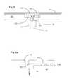
- FIG. 11shows a seventh embodiment which is the same as the first embodiment except as described below.
- the object on the substrate table WTis a sensor 220 such as a transmission image sensor (TIS).
- a bead of glue 700which is undissolvable and unreactable with the immersion fluid is positioned between the edge seal member 117 and the sensor 220 .
- the glueis covered by immersion fluid in use.
- FIGS. 12 and 13An eighth embodiment is described with reference to FIGS. 12 and 13 .
- the eighth embodimentit is a sensor 220 which is being sealed to the substrate table WT.
- a vacuum 46is provided adjacent the gap with an opening passage 47 and a chamber 44 for taking away any immersion liquid which should find its way through the gap between the edge seal member 117 and the edge of the sensor 220 .
- the vacuum 46is provided in the substrate table WT under an overhang portion of the object 220 .
- the passage 47is provided in an overhanging inwardly protruding portion of the substrate table WT.
- a bead of glue 700is positioned at the inner most edge of the protruding portion between the substrate table WT and the object 220 . If no bead of glue 700 is provided, a flow of gas from underneath the object 220 helps seal the gap between the sensor 220 and the substrate table WT.
- the vacuum 46 , compartment 44 and passage 47are provided in the object 220 itself under an inwardly protruding edge seal member 117 . Again there is the option of providing a bead of glue between the object 220 and the substrate table WT radially outwardly of the passage 47 .
- edge seal member 117 and the top outer most edge of the object 220can be varied. For example, it may be advantageous to provide an overhanging edge seal member 117 or indeed an outer edge of the object 220 which is overhanging. Alternatively, an outer upper corner of the object 220 may be useful.
- Substrate-level sensorsmay comprise a radiation-receiving element ( 1102 , 1118 ) and a radiation-detecting element ( 1108 , 1124 ) as shown in FIGS. 16-19 .
- Exposure radiationis directed from the final element of the projection system PL through an immersion liquid 11 at least partly filling a space between the final element of the projection system PL and the substrate W.
- the detailed configuration of each of these elementsdepends on the properties of the radiation to be detected.
- the sensor at substrate levelmay comprise a photocell only, for use in cases where it is desirable for the photocell to receive the radiation directly.
- the sensor at substrate levelmay comprise a luminescence layer in combination with a photocell. In this arrangement, radiation at a first wavelength is absorbed by the luminescence layer and reradiated a short time later at a second (longer) wavelength. This arrangement is useful, for example, where the photocell is designed to work more efficiently at the second wavelength.
- arrangementsare provided so that gas is excluded from the region between the radiation-receiving ( 1102 , 1118 ) and radiation-detecting ( 1108 , 1124 ) elements in order to avoid interfaces between media of high refractive index and gas.
- absorptionmay also seriously reduce the intensity of radiation intensity reaching the photocell, as may scattering from interfaces that are not optically smooth.
- FIG. 16shows an integrated lens interferometer and scanner (ILIAS) sensor module.
- This modulehas a shearing grating structure 1102 as a radiation-receiving element, supported by a transmissive plate 1104 , which may be made of glass or quartz.
- a quantum conversion layer 1106is positioned immediately above a camera chip 1108 (the radiation-detecting element), which is in turn mounted on a substrate 1110 .
- the substrate 1110is connected to the transmissive plate 1104 via spacers 1112 and bonding wires 1114 connect the radiation-detecting element to external instrumentation.
- a gas gapis located between the quantum conversion layer 1106 and the transmissive plate 1104 .
- the gas gap within the sensorcannot easily be purged so that it will contain significant proportions of oxygen and water, which absorb radiation. Signal is therefore lost and the effect becomes worse for larger angles as these have a longer path length through gas. Thus, the dynamic range requirements for the sensor become more severe.
- FIGS. 17 and 18show improved ILIAS sensor modules according to embodiments of the present invention.
- the gas gaphas been removed by changing the shape of the transmissive plate 1104 to fit directly to the camera 1108 .
- This arrangementis made more difficult by the need to provide access for the bonding wires 1114 and necessitates an elongated form.
- the alternative arrangement shown in FIG. 18is easier to realize.
- a filler sheet 1116 of the same material as the transmissive plate 1104 , or of similar optical properties,is inserted between the transmissive plate 1104 and the quantum conversion layer 1106 .
- the removal of the gas gapreduces transmission losses and relaxes dynamic range requirements (or, alternatively speaking, improves the effective dynamic range). Both arrangements improve refractive index matching and reduce the extent of spurious internal reflections at the interface with the transmissive plate 1104 .
- FIG. 19 ashows a DUV transmission image sensor.
- FIG. 19 bshows a magnified view of the processing element for clarity.
- the pattern of transmissive grooves 1118constituting the radiation-receiving element in this case, is realized by means of e-beam lithography and dry etching techniques in a thin metal layer deposited on a substrate by means of sputtering.
- DUV radiation that is projected towards the grooves 1118is transmitted by the transmissive plate 1104 (which may be quartz or fused silica) and hits the underlying luminescent material 1122 , or “phosphor”.
- the luminescent material 1122may comprise a slab of crystalline material that is doped with rare-earth ions, e.g.
- the main purpose of the luminescent material 1122is to convert the DUV radiation into more easily detectable visible radiation, which is then detected by the photodiode 1124 .
- DUV radiation that has not been absorbed and converted into visible radiation by the phosphor 1122may be filtered out before it reaches the photodiode 1124 (e.g. by a BG-39 or UG filter 1126 ).
- gasmay be present in the gaps between components mounted in the sensor housing 1125 , yielding a number of gas/material/gas interfaces that interrupt the propagation of radiation.
- the first region of interestis the rear-side 1128 of the transmissive plate 1104 , reached by DUV radiation after it has passed through the grooves 1118 and transmissive plate 1104 .
- the surfacehas been formed by mechanical means, such as by drilling, and is inevitably rough on the scale of the wavelength of the radiation. Radiation may therefore be lost due to scattering, either back into the transmissive plate 1104 or out past the luminescent material 1122 .
- the DUV lightencounters the optically smooth gas/YAG:Ce interface, where a substantial amount of reflection may occur due to the refractive index mismatch, particularly in systems of high NA.
- the luminescent material 1122emits radiation in random directions. Due to its relatively high refractive index, the critical angle for total internal reflection at a YAG:Ce/air boundary is around 33° (where, for example, there is air in the gap between the YAG:Ce and the filter 1126 ) from the normal, meaning that a large proportion of radiation incident on the boundary is reflected out of the system and lost through the side walls of the luminescent material 1122 . Finally, the part of the luminescence that is directed towards the photodiode has to overcome the gas/quartz interface on the diode surface where surface roughness may again account for loss of detected signal.
- each of the embodimentsmay be combined with one or more of the other embodiments as appropriate. Further, each of the embodiments (and any appropriate combination of embodiments) can be applied simply to the liquid supply system of FIG. 2 and FIGS. 14 and 15 without the edge seal member 17 , 117 as feasible and/or appropriate.
- a lithographic projection apparatuscomprising: an illuminator adapted to condition a beam of radiation; a support structure configured to hold a patterning device, the patterning device configured to pattern the beam of radiation according to a desired pattern; a substrate table configured to hold a substrate; a projection system adapted to project the patterned beam onto a target portion of a substrate; a liquid supply system configured to at least partly fill a space between the projection system and an object on the substrate table, with a liquid; and a sensor capable of being positioned to be illuminated by a beam of radiation once it has passed through the liquid.
- the substrate tablecomprises a support surface configured to support an intermediary plate between the projection system and the sensor and not in contact with the sensor.
- the sensorcomprises a transmission image sensor configured to sense the beam and wherein the intermediary plate is positionable between the sensor and the projection system.
- the sensoris on the substrate table.
- the sensorcomprises an alignment sensor configured to align the substrate table relative to the projection system.
- measurement gratings of the alignment sensorhave a pitch of less than 500 nm.
- the alignment sensoris configured to be illuminated obliquely.
- the sensorcomprises a transmission image sensor.
- the sensorcomprises a focus sensor.
- the senorcomprises a spot or dose sensor, an integrated lens interferometer and scanner, an alignment mark, or any combination of the foregoing.
- the substrate tablecomprises an edge seal member configured to at least partly surround an edge of the sensor and to provide a primary surface facing the projection system substantially co-planar with a primary surface of the sensor.
- the sensoris configured to be in contact with the liquid and the beam of radiation is configured to come from the projection system or an alignment system.
- the beam of radiationis the patterned beam.
- an alignment systemcomprises the sensor and is configured receive an alignment beam of radiation from the projection system to align the substrate.
- the substrate tablecomprises a vacuum port configured to remove liquid from a space between the substrate table and the sensor.
- the apparatusfurther comprises a bead of material in a space between the substrate table and the sensor configured to prevent entry of the liquid.
- a device manufacturing methodcomprising: projecting a beam of radiation through a liquid onto a sensor; and projecting the beam of radiation as patterned using a projection system of a lithographic apparatus through the liquid onto a target portion of a substrate.
- the liquidis supported on an intermediary plate between the projection system and the sensor, the plate not being in contact with the sensor.
- the sensorcomprises a transmission image sensor configured to sense the beam and the intermediary plate is positionable between the sensor and the projection system.
- the sensoris on a substrate table holding the substrate.
- the sensorcomprises an alignment sensor configured to align a substrate table holding the substrate relative to the projection system.
- measurement gratings of the alignment sensorhave a pitch of less than 500 nm.
- the alignment sensoris configured to be illuminated obliquely.
- the sensorcomprises a transmission image sensor.
- the sensorcomprises a focus sensor.
- the senorcomprises a spot or dose sensor, an integrated lens interferometer and scanner, an alignment mark, or any combination of the foregoing.
- a substrate table holding the substratecomprises an edge seal member configured to at least partly surround an edge of the sensor and to provide a primary surface facing the projection system substantially co-planar with a primary surface of the sensor.
- the methodcomprises projecting the beam of radiation from the projection system or an alignment system through the liquid onto the sensor in contact with the liquid.
- the beam of radiationis the patterned beam.
- an alignment systemcomprises the sensor and is configured receive an alignment beam of radiation from the projection system to align the substrate.
- a substrate table holding the substratecomprises a vacuum port configured to remove liquid from a space between the substrate table and the sensor.
- the methodfurther comprises providing a bead of material in a space between the substrate table and the sensor configured to prevent entry of the liquid.
- the inventionmay be practiced otherwise than as described.
- the inventionis also applicable to other types of liquid supply systems, especially localised liquid area systems.
- the seal member solutionit may be one in which a seal other than a gas seal is used. The description is not intended to limit the invention.
Landscapes
- Physics & Mathematics (AREA)
- General Physics & Mathematics (AREA)
- Health & Medical Sciences (AREA)
- Engineering & Computer Science (AREA)
- Environmental & Geological Engineering (AREA)
- Epidemiology (AREA)
- Public Health (AREA)
- Life Sciences & Earth Sciences (AREA)
- Atmospheric Sciences (AREA)
- Toxicology (AREA)
- Exposure And Positioning Against Photoresist Photosensitive Materials (AREA)
- Exposure Of Semiconductors, Excluding Electron Or Ion Beam Exposure (AREA)
Abstract
Description
- a radiation system Ex, IL, for supplying a projection beam PB of radiation (e.g. DUV radiation), which in this particular case also comprises a radiation source LA;
- a first object table (mask table) MT provided with a mask holder for holding a mask MA (e.g. a reticle), and connected to a first positioning device for accurately positioning the mask with respect to item PL;
- a second object table (substrate table) WT provided with a substrate holder for holding a substrate W (e.g. a resist-coated silicon wafer), and connected to a second positioning device for accurately positioning the substrate with respect to item PL;
- a projection system (“projection lens”) PL (e.g. a refractive system) for imaging an irradiated portion of the mask MA onto a target portion C (e.g. comprising one or more dies) of the substrate W.
Claims (20)
Priority Applications (1)
| Application Number | Priority Date | Filing Date | Title |
|---|---|---|---|
| US13/195,248US9081299B2 (en) | 2003-06-09 | 2011-08-01 | Lithographic apparatus and device manufacturing method involving removal of liquid entering a gap |
Applications Claiming Priority (14)
| Application Number | Priority Date | Filing Date | Title |
|---|---|---|---|
| EP03253636.9 | 2003-06-09 | ||
| EP03253636 | 2003-06-09 | ||
| EP03253636 | 2003-06-09 | ||
| EP03255395 | 2003-08-29 | ||
| EP03255395 | 2003-08-29 | ||
| EP03255395.0 | 2003-08-29 | ||
| EP03257068 | 2003-11-10 | ||
| EP03257068.1AEP1429188B1 (en) | 2002-11-12 | 2003-11-10 | Lithographic projection apparatus |
| EP03257068.1 | 2003-11-10 | ||
| US10/857,614US7213963B2 (en) | 2003-06-09 | 2004-06-01 | Lithographic apparatus and device manufacturing method |
| US11/482,122US8154708B2 (en) | 2003-06-09 | 2006-07-07 | Lithographic apparatus and device manufacturing method |
| US12/698,932US8482845B2 (en) | 2003-06-09 | 2010-02-02 | Lithographic apparatus and device manufacturing method |
| US13/194,136US9152058B2 (en) | 2003-06-09 | 2011-07-29 | Lithographic apparatus and device manufacturing method involving a member and a fluid opening |
| US13/195,248US9081299B2 (en) | 2003-06-09 | 2011-08-01 | Lithographic apparatus and device manufacturing method involving removal of liquid entering a gap |
Related Parent Applications (1)
| Application Number | Title | Priority Date | Filing Date |
|---|---|---|---|
| US13/194,136ContinuationUS9152058B2 (en) | 2003-06-09 | 2011-07-29 | Lithographic apparatus and device manufacturing method involving a member and a fluid opening |
Publications (2)
| Publication Number | Publication Date |
|---|---|
| US20110285977A1 US20110285977A1 (en) | 2011-11-24 |
| US9081299B2true US9081299B2 (en) | 2015-07-14 |
Family
ID=34108333
Family Applications (8)
| Application Number | Title | Priority Date | Filing Date |
|---|---|---|---|
| US10/857,614Expired - LifetimeUS7213963B2 (en) | 2003-06-09 | 2004-06-01 | Lithographic apparatus and device manufacturing method |
| US11/482,122Expired - Fee RelatedUS8154708B2 (en) | 2003-06-09 | 2006-07-07 | Lithographic apparatus and device manufacturing method |
| US12/698,932Expired - Fee RelatedUS8482845B2 (en) | 2003-06-09 | 2010-02-02 | Lithographic apparatus and device manufacturing method |
| US13/194,136Expired - Fee RelatedUS9152058B2 (en) | 2003-06-09 | 2011-07-29 | Lithographic apparatus and device manufacturing method involving a member and a fluid opening |
| US13/195,248Expired - Fee RelatedUS9081299B2 (en) | 2003-06-09 | 2011-08-01 | Lithographic apparatus and device manufacturing method involving removal of liquid entering a gap |
| US13/306,532Expired - Fee RelatedUS9541843B2 (en) | 2003-06-09 | 2011-11-29 | Lithographic apparatus and device manufacturing method involving a sensor detecting a radiation beam through liquid |
| US15/385,584Expired - Fee RelatedUS10180629B2 (en) | 2003-06-09 | 2016-12-20 | Lithographic apparatus and device manufacturing method |
| US16/245,400Expired - LifetimeUS10678139B2 (en) | 2003-06-09 | 2019-01-11 | Lithographic apparatus and device manufacturing method |
Family Applications Before (4)
| Application Number | Title | Priority Date | Filing Date |
|---|---|---|---|
| US10/857,614Expired - LifetimeUS7213963B2 (en) | 2003-06-09 | 2004-06-01 | Lithographic apparatus and device manufacturing method |
| US11/482,122Expired - Fee RelatedUS8154708B2 (en) | 2003-06-09 | 2006-07-07 | Lithographic apparatus and device manufacturing method |
| US12/698,932Expired - Fee RelatedUS8482845B2 (en) | 2003-06-09 | 2010-02-02 | Lithographic apparatus and device manufacturing method |
| US13/194,136Expired - Fee RelatedUS9152058B2 (en) | 2003-06-09 | 2011-07-29 | Lithographic apparatus and device manufacturing method involving a member and a fluid opening |
Family Applications After (3)
| Application Number | Title | Priority Date | Filing Date |
|---|---|---|---|
| US13/306,532Expired - Fee RelatedUS9541843B2 (en) | 2003-06-09 | 2011-11-29 | Lithographic apparatus and device manufacturing method involving a sensor detecting a radiation beam through liquid |
| US15/385,584Expired - Fee RelatedUS10180629B2 (en) | 2003-06-09 | 2016-12-20 | Lithographic apparatus and device manufacturing method |
| US16/245,400Expired - LifetimeUS10678139B2 (en) | 2003-06-09 | 2019-01-11 | Lithographic apparatus and device manufacturing method |
Country Status (6)
| Country | Link |
|---|---|
| US (8) | US7213963B2 (en) |
| JP (7) | JP4199699B2 (en) |
| KR (1) | KR100683263B1 (en) |
| CN (2) | CN102147574B (en) |
| SG (2) | SG116555A1 (en) |
| TW (2) | TWI304159B (en) |
Families Citing this family (140)
| Publication number | Priority date | Publication date | Assignee | Title |
|---|---|---|---|---|
| US9482966B2 (en) | 2002-11-12 | 2016-11-01 | Asml Netherlands B.V. | Lithographic apparatus and device manufacturing method |
| KR100585476B1 (en)* | 2002-11-12 | 2006-06-07 | 에이에스엠엘 네델란즈 비.브이. | Lithographic Apparatus and Device Manufacturing Method |
| DE60335595D1 (en) | 2002-11-12 | 2011-02-17 | Asml Netherlands Bv | Immersion lithographic apparatus and method of making a device |
| CN100568101C (en) | 2002-11-12 | 2009-12-09 | Asml荷兰有限公司 | Photolithography apparatus and device manufacturing method |
| US7110081B2 (en) | 2002-11-12 | 2006-09-19 | Asml Netherlands B.V. | Lithographic apparatus and device manufacturing method |
| US10503084B2 (en) | 2002-11-12 | 2019-12-10 | Asml Netherlands B.V. | Lithographic apparatus and device manufacturing method |
| SG121822A1 (en) | 2002-11-12 | 2006-05-26 | Asml Netherlands Bv | Lithographic apparatus and device manufacturing method |
| DE10261775A1 (en) | 2002-12-20 | 2004-07-01 | Carl Zeiss Smt Ag | Device for the optical measurement of an imaging system |
| EP2466623B1 (en) | 2003-02-26 | 2015-04-22 | Nikon Corporation | Exposure apparatus, exposure method, and method for producing device |
| EP3062152B1 (en) | 2003-04-10 | 2017-12-20 | Nikon Corporation | Environmental system including vaccum scavenge for an immersion lithography apparatus |
| EP2950147B1 (en) | 2003-04-10 | 2017-04-26 | Nikon Corporation | Environmental system including vaccum scavenge for an immersion lithography apparatus |
| KR101225884B1 (en) | 2003-04-11 | 2013-01-28 | 가부시키가이샤 니콘 | Apparatus and method for maintaining immersion fluid in the gap under the projection lens during wafer exchange in an immersion lithography machine |
| US7213963B2 (en) | 2003-06-09 | 2007-05-08 | Asml Netherlands B.V. | Lithographic apparatus and device manufacturing method |
| EP2261741A3 (en) | 2003-06-11 | 2011-05-25 | ASML Netherlands B.V. | Lithographic apparatus and device manufacturing method |
| KR101242815B1 (en) | 2003-06-13 | 2013-03-12 | 가부시키가이샤 니콘 | Exposure method, substrate stage, exposure apparatus and method for manufacturing device |
| TW201721717A (en) | 2003-06-19 | 2017-06-16 | 尼康股份有限公司 | Exposure apparatus, exposure method, and device manufacturing method |
| KR20060027832A (en) | 2003-07-01 | 2006-03-28 | 가부시키가이샤 니콘 | Method of Using Isotopically Specified Fluids as Optical Elements |
| EP3179309A1 (en) | 2003-07-08 | 2017-06-14 | Nikon Corporation | Wafer table for immersion lithography |
| EP1643543B1 (en) | 2003-07-09 | 2010-11-24 | Nikon Corporation | Exposure apparatus and method for manufacturing device |
| WO2005006418A1 (en)* | 2003-07-09 | 2005-01-20 | Nikon Corporation | Exposure apparatus and method for manufacturing device |
| WO2005006415A1 (en) | 2003-07-09 | 2005-01-20 | Nikon Corporation | Exposure apparatus and method for manufacturing device |
| SG109000A1 (en)* | 2003-07-16 | 2005-02-28 | Asml Netherlands Bv | Lithographic apparatus and device manufacturing method |
| EP1500982A1 (en)* | 2003-07-24 | 2005-01-26 | ASML Netherlands B.V. | Lithographic apparatus and device manufacturing method |
| WO2005010960A1 (en) | 2003-07-25 | 2005-02-03 | Nikon Corporation | Inspection method and inspection device for projection optical system, and production method for projection optical system |
| KR101641011B1 (en) | 2003-07-28 | 2016-07-19 | 가부시키가이샤 니콘 | Exposure apparatus, device producing method, and exposure apparatus controlling method |
| EP1503244A1 (en) | 2003-07-28 | 2005-02-02 | ASML Netherlands B.V. | Lithographic projection apparatus and device manufacturing method |
| US7779781B2 (en) | 2003-07-31 | 2010-08-24 | Asml Netherlands B.V. | Lithographic apparatus and device manufacturing method |
| KR101475995B1 (en)* | 2003-08-21 | 2014-12-23 | 가부시키가이샤 니콘 | Exposure apparatus, exposure method, and device producing method |
| TWI245163B (en) | 2003-08-29 | 2005-12-11 | Asml Netherlands Bv | Lithographic apparatus and device manufacturing method |
| KR101380989B1 (en) | 2003-08-29 | 2014-04-04 | 가부시키가이샤 니콘 | Exposure apparatus and device producing method |
| TWI263859B (en) | 2003-08-29 | 2006-10-11 | Asml Netherlands Bv | Lithographic apparatus and device manufacturing method |
| EP3223053A1 (en)* | 2003-09-03 | 2017-09-27 | Nikon Corporation | Apparatus and method for providing fluid for immersion lithography |
| JP4444920B2 (en) | 2003-09-19 | 2010-03-31 | 株式会社ニコン | Exposure apparatus and device manufacturing method |
| EP2837969B1 (en) | 2003-09-29 | 2016-04-20 | Nikon Corporation | Exposure apparatus, exposure method, and method for producing device |
| KR20060126949A (en) | 2003-10-08 | 2006-12-11 | 가부시키가이샤 니콘 | Substrate conveyance apparatus and substrate conveyance method, exposure apparatus, exposure method, and device manufacturing method |
| JP2005136364A (en) | 2003-10-08 | 2005-05-26 | Zao Nikon Co Ltd | Substrate transport apparatus, exposure apparatus, and device manufacturing method |
| KR101203028B1 (en) | 2003-10-08 | 2012-11-21 | 가부시키가이샤 자오 니콘 | Substrate carrying apparatus, substrate carrying method, exposure apparatus, exposure method, and method for producing device |
| TWI553701B (en) | 2003-10-09 | 2016-10-11 | 尼康股份有限公司 | Exposure apparatus and exposure method, component manufacturing method |
| CN100461336C (en)* | 2003-10-31 | 2009-02-11 | 株式会社尼康 | Exposure apparatus and device manufacturing method |
| CN1890779B (en)* | 2003-12-03 | 2011-06-08 | 株式会社尼康 | Exposure apparatus, exposure method and device manufacturing method |
| KR101394764B1 (en) | 2003-12-03 | 2014-05-27 | 가부시키가이샤 니콘 | Exposure apparatus, exposure method, device producing method, and optical component |
| JP4513534B2 (en)* | 2003-12-03 | 2010-07-28 | 株式会社ニコン | Exposure apparatus, exposure method, and device manufacturing method |
| JP2005175016A (en)* | 2003-12-08 | 2005-06-30 | Canon Inc | Substrate holding apparatus, exposure apparatus using the same, and device manufacturing method |
| JP4720506B2 (en) | 2003-12-15 | 2011-07-13 | 株式会社ニコン | Stage apparatus, exposure apparatus, and exposure method |
| US7589822B2 (en) | 2004-02-02 | 2009-09-15 | Nikon Corporation | Stage drive method and stage unit, exposure apparatus, and device manufacturing method |
| WO2005076321A1 (en) | 2004-02-03 | 2005-08-18 | Nikon Corporation | Exposure apparatus and method of producing device |
| JP4018647B2 (en)* | 2004-02-09 | 2007-12-05 | キヤノン株式会社 | Projection exposure apparatus and device manufacturing method |
| US7050146B2 (en) | 2004-02-09 | 2006-05-23 | Asml Netherlands B.V. | Lithographic apparatus and device manufacturing method |
| KR101851511B1 (en)* | 2004-03-25 | 2018-04-23 | 가부시키가이샤 니콘 | Exposure apparatus and method for manufacturing device |
| US7034917B2 (en)* | 2004-04-01 | 2006-04-25 | Asml Netherlands B.V. | Lithographic apparatus, device manufacturing method and device manufactured thereby |
| US7898642B2 (en) | 2004-04-14 | 2011-03-01 | Asml Netherlands B.V. | Lithographic apparatus and device manufacturing method |
| US8054448B2 (en) | 2004-05-04 | 2011-11-08 | Nikon Corporation | Apparatus and method for providing fluid for immersion lithography |
| US7486381B2 (en)* | 2004-05-21 | 2009-02-03 | Asml Netherlands B.V. | Lithographic apparatus and device manufacturing method |
| CN100594430C (en) | 2004-06-04 | 2010-03-17 | 卡尔蔡司Smt股份公司 | System for measuring image quality of optical imaging system |
| JP4826146B2 (en)* | 2004-06-09 | 2011-11-30 | 株式会社ニコン | Exposure apparatus and device manufacturing method |
| KR101227290B1 (en) | 2004-06-09 | 2013-01-29 | 가부시키가이샤 니콘 | Substrate holding device, exposure apparatus having same, exposure method, method for producing device, and liquid repellent plate |
| US8508713B2 (en)* | 2004-06-10 | 2013-08-13 | Nikon Corporation | Exposure apparatus, exposure method, and method for producing device |
| KR101178755B1 (en)* | 2004-06-10 | 2012-08-31 | 가부시키가이샤 니콘 엔지니어링 | Exposure equipment, exposure method and device manufacturing method |
| US8717533B2 (en)* | 2004-06-10 | 2014-05-06 | Nikon Corporation | Exposure apparatus, exposure method, and method for producing device |
| US8373843B2 (en)* | 2004-06-10 | 2013-02-12 | Nikon Corporation | Exposure apparatus, exposure method, and method for producing device |
| US7517639B2 (en)* | 2004-06-23 | 2009-04-14 | Taiwan Semiconductor Manufacturing Co., Ltd. | Seal ring arrangements for immersion lithography systems |
| US7501226B2 (en)* | 2004-06-23 | 2009-03-10 | Taiwan Semiconductor Manufacturing Co., Ltd. | Immersion lithography system with wafer sealing mechanisms |
| US7463330B2 (en) | 2004-07-07 | 2008-12-09 | Asml Netherlands B.V. | Lithographic apparatus and device manufacturing method |
| JP4894515B2 (en) | 2004-07-12 | 2012-03-14 | 株式会社ニコン | Exposure apparatus, device manufacturing method, and liquid detection method |
| JP4752375B2 (en)* | 2004-08-03 | 2011-08-17 | 株式会社ニコン | Exposure apparatus, exposure method, and device manufacturing method |
| US8169591B2 (en)* | 2004-08-03 | 2012-05-01 | Nikon Corporation | Exposure apparatus, exposure method, and method for producing device |
| KR20070048164A (en) | 2004-08-18 | 2007-05-08 | 가부시키가이샤 니콘 | Exposure apparatus and device manufacturing method |
| US7701550B2 (en) | 2004-08-19 | 2010-04-20 | Asml Netherlands B.V. | Lithographic apparatus and device manufacturing method |
| SG10201801998TA (en) | 2004-09-17 | 2018-04-27 | Nikon Corp | Substrate holding device, exposure apparatus, and device manufacturing method |
| TWI588872B (en)* | 2004-11-18 | 2017-06-21 | 尼康股份有限公司 | Position measurement method, position control method, measurement method, loading method, exposure method and exposure apparatus, and device manufacturing method |
| US7397533B2 (en) | 2004-12-07 | 2008-07-08 | Asml Netherlands B.V. | Lithographic apparatus and device manufacturing method |
| US7880860B2 (en) | 2004-12-20 | 2011-02-01 | Asml Netherlands B.V. | Lithographic apparatus and device manufacturing method |
| JP2006173527A (en)* | 2004-12-20 | 2006-06-29 | Sony Corp | Exposure equipment |
| JP2006202825A (en)* | 2005-01-18 | 2006-08-03 | Jsr Corp | Immersion exposure equipment |
| US8692973B2 (en) | 2005-01-31 | 2014-04-08 | Nikon Corporation | Exposure apparatus and method for producing device |
| KR101513840B1 (en) | 2005-01-31 | 2015-04-20 | 가부시키가이샤 니콘 | Exposure apparatus and method for manufacturing device |
| US7282701B2 (en) | 2005-02-28 | 2007-10-16 | Asml Netherlands B.V. | Sensor for use in a lithographic apparatus |
| USRE43576E1 (en) | 2005-04-08 | 2012-08-14 | Asml Netherlands B.V. | Dual stage lithographic apparatus and device manufacturing method |
| US7433016B2 (en)* | 2005-05-03 | 2008-10-07 | Asml Netherlands B.V. | Lithographic apparatus and device manufacturing method |
| US7268357B2 (en)* | 2005-05-16 | 2007-09-11 | Taiwan Semiconductor Manufacturing Company, Ltd. | Immersion lithography apparatus and method |
| JP2006339448A (en)* | 2005-06-02 | 2006-12-14 | Canon Inc | Exposure apparatus having a light receiving unit |
| JP4708876B2 (en)* | 2005-06-21 | 2011-06-22 | キヤノン株式会社 | Immersion exposure equipment |
| US8054445B2 (en)* | 2005-08-16 | 2011-11-08 | Asml Netherlands B.V. | Lithographic apparatus and device manufacturing method |
| JP4883467B2 (en)* | 2005-09-08 | 2012-02-22 | 株式会社ニコン | Light quantity measuring apparatus, exposure apparatus, and device manufacturing method |
| FR2890742B1 (en)* | 2005-09-12 | 2007-11-30 | Production Et De Rech S Appliq | EQUIPMENT AND METHOD FOR MONITORING A LITHOGRAPHIC IMMERSION DEVICE. |
| JP3997245B2 (en)* | 2005-10-04 | 2007-10-24 | キヤノン株式会社 | Exposure apparatus and device manufacturing method |
| JP3997244B2 (en)* | 2005-10-04 | 2007-10-24 | キヤノン株式会社 | Exposure apparatus and device manufacturing method |
| JP4125315B2 (en)* | 2005-10-11 | 2008-07-30 | キヤノン株式会社 | Exposure apparatus and device manufacturing method |
| US7564536B2 (en)* | 2005-11-08 | 2009-07-21 | Asml Netherlands B.V. | Lithographic apparatus and device manufacturing method |
| JPWO2007055237A1 (en)* | 2005-11-09 | 2009-04-30 | 株式会社ニコン | Exposure apparatus, exposure method, and device manufacturing method |
| US7633073B2 (en) | 2005-11-23 | 2009-12-15 | Asml Netherlands B.V. | Lithographic apparatus and device manufacturing method |
| US7649611B2 (en) | 2005-12-30 | 2010-01-19 | Asml Netherlands B.V. | Lithographic apparatus and device manufacturing method |
| US7787101B2 (en)* | 2006-02-16 | 2010-08-31 | International Business Machines Corporation | Apparatus and method for reducing contamination in immersion lithography |
| US8027019B2 (en) | 2006-03-28 | 2011-09-27 | Asml Netherlands B.V. | Lithographic apparatus and device manufacturing method |
| JP2007266504A (en)* | 2006-03-29 | 2007-10-11 | Canon Inc | Exposure equipment |
| US7388652B2 (en)* | 2006-06-15 | 2008-06-17 | Asml Netherlands B.V. | Wave front sensor with grey filter and lithographic apparatus comprising same |
| US7804582B2 (en)* | 2006-07-28 | 2010-09-28 | Asml Netherlands B.V. | Lithographic apparatus, method of calibrating a lithographic apparatus and device manufacturing method |
| US8253922B2 (en) | 2006-11-03 | 2012-08-28 | Taiwan Semiconductor Manufacturing Company, Ltd. | Immersion lithography system using a sealed wafer bath |
| US8208116B2 (en)* | 2006-11-03 | 2012-06-26 | Taiwan Semiconductor Manufacturing Company, Ltd. | Immersion lithography system using a sealed wafer bath |
| JP2008147577A (en)* | 2006-12-13 | 2008-06-26 | Canon Inc | Exposure apparatus and device manufacturing method |
| US8817226B2 (en) | 2007-02-15 | 2014-08-26 | Asml Holding N.V. | Systems and methods for insitu lens cleaning using ozone in immersion lithography |
| US8654305B2 (en) | 2007-02-15 | 2014-02-18 | Asml Holding N.V. | Systems and methods for insitu lens cleaning in immersion lithography |
| US8514365B2 (en)* | 2007-06-01 | 2013-08-20 | Asml Netherlands B.V. | Lithographic apparatus and device manufacturing method |
| US20090002656A1 (en)* | 2007-06-29 | 2009-01-01 | Asml Netherlands B.V. | Device and method for transmission image detection, lithographic apparatus and mask for use in a lithographic apparatus |
| JP4961299B2 (en)* | 2007-08-08 | 2012-06-27 | キヤノン株式会社 | Exposure apparatus and device manufacturing method |
| US8681308B2 (en)* | 2007-09-13 | 2014-03-25 | Asml Netherlands B.V. | Lithographic apparatus and device manufacturing method |
| JP4533416B2 (en)* | 2007-09-25 | 2010-09-01 | キヤノン株式会社 | Exposure apparatus and device manufacturing method |
| NL1036432A1 (en)* | 2008-01-23 | 2009-07-27 | Asml Holding Nv | An immersion lithographic apparatus with immersion fluid re-circulating system. |
| WO2009115979A1 (en)* | 2008-03-16 | 2009-09-24 | Nxp B.V. | Methods, circuits, systems and arrangements for undriven or driven pins |
| NL1036898A1 (en)* | 2008-05-21 | 2009-11-24 | Asml Netherlands Bv | Substrate table, sensor and method. |
| US9176393B2 (en) | 2008-05-28 | 2015-11-03 | Asml Netherlands B.V. | Lithographic apparatus and a method of operating the apparatus |
| NL2003575A (en)* | 2008-10-29 | 2010-05-03 | Asml Netherlands Bv | Lithographic apparatus and device manufacturing method. |
| JP5833927B2 (en)* | 2008-11-11 | 2015-12-16 | ウィラ・ベスローテン・フェンノートシャップWila B.V. | Device for clamping tools |
| JP5199982B2 (en) | 2008-12-08 | 2013-05-15 | エーエスエムエル ネザーランズ ビー.ブイ. | Lithographic apparatus |
| NL2004242A (en)* | 2009-04-13 | 2010-10-14 | Asml Netherlands Bv | Detector module, cooling arrangement and lithographic apparatus comprising a detector module. |
| NL2004322A (en)* | 2009-04-13 | 2010-10-14 | Asml Netherlands Bv | Cooling device, cooling arrangement and lithographic apparatus comprising a cooling arrangement. |
| NL2004807A (en)* | 2009-06-30 | 2011-01-04 | Asml Netherlands Bv | Substrate table for a lithographic apparatus, litographic apparatus, method of using a substrate table and device manufacturing method. |
| NL2005528A (en)* | 2009-12-02 | 2011-06-07 | Asml Netherlands Bv | Lithographic apparatus and device manufacturing method. |
| KR101686549B1 (en)* | 2010-02-19 | 2016-12-14 | 마퍼 리쏘그라피 아이피 비.브이. | Substrate support structure, clamp preparation unit, and lithography system |
| NL2006244A (en)* | 2010-03-16 | 2011-09-19 | Asml Netherlands Bv | Lithographic apparatus, cover for use in a lithographic apparatus and method for designing a cover for use in a lithographic apparatus. |
| NL2006203A (en)* | 2010-03-16 | 2011-09-19 | Asml Netherlands Bv | Cover for a substrate table, substrate table for a lithographic apparatus, lithographic apparatus, and device manufacturing method. |
| JP5313293B2 (en)* | 2010-05-19 | 2013-10-09 | エーエスエムエル ネザーランズ ビー.ブイ. | Lithographic apparatus, fluid handling structure used in lithographic apparatus, and device manufacturing method |
| NL2007802A (en) | 2010-12-21 | 2012-06-25 | Asml Netherlands Bv | A substrate table, a lithographic apparatus and a device manufacturing method. |
| NL2008980A (en) | 2011-07-11 | 2013-01-14 | Asml Netherlands Bv | A fluid handling structure, a lithographic apparatus and a device manufacturing method. |
| NL2008979A (en) | 2011-07-11 | 2013-01-14 | Asml Netherlands Bv | A fluid handling structure, a lithographic apparatus and a device manufacturing method. |
| CN102914946B (en)* | 2011-08-04 | 2016-04-20 | 上海微电子装备有限公司 | A kind of energy sensor of photomask processor |
| JP5778093B2 (en) | 2011-08-10 | 2015-09-16 | エーエスエムエル ネザーランズ ビー.ブイ. | Substrate table assembly, immersion lithographic apparatus and device manufacturing method |
| KR102003416B1 (en) | 2012-05-29 | 2019-07-24 | 에이에스엠엘 네델란즈 비.브이. | Support apparatus, lithographic apparatus and device manufacturing method |
| KR102054322B1 (en) | 2012-05-29 | 2019-12-10 | 에이에스엠엘 네델란즈 비.브이. | Object holder and lithographic apparatus |
| NL2011568A (en)* | 2012-10-31 | 2014-05-06 | Asml Netherlands Bv | Sensor and lithographic apparatus. |
| CN103176368B (en)* | 2013-03-06 | 2014-12-10 | 浙江大学 | Gas-seal and gas-liquid vibration damping recovery device used in immersion lithographic machine |
| US10082424B2 (en) | 2014-05-07 | 2018-09-25 | Asml Netherlands B.V. | Diamond-based monitoring apparatus for lithographic apparatus, and a lithographic apparatus comprising diamond-based monitoring apparatus |
| WO2015188988A1 (en) | 2014-06-10 | 2015-12-17 | Asml Netherlands B.V. | Lithographic apparatus and method of manufacturing a lithographic apparatus |
| WO2016000883A1 (en)* | 2014-07-04 | 2016-01-07 | Asml Netherlands B.V. | Lithographic apparatus and a method of manufacturing a device using a lithographic apparatus |
| NL2015178A (en) | 2014-08-06 | 2016-07-08 | Asml Netherlands Bv | A Lithographic Apparatus and a Method of Manufacturing a Lithographic Apparatus. |
| US10578959B2 (en) | 2015-04-29 | 2020-03-03 | Asml Netherlands B.V. | Support apparatus, lithographic apparatus and device manufacturing method |
| NL2017014A (en) | 2015-06-23 | 2016-12-29 | Asml Netherlands Bv | A Support Apparatus, a Lithographic Apparatus and a Device Manufacturing Method |
| US10317804B2 (en) | 2015-12-08 | 2019-06-11 | Asml Netherlands B.V. | Substrate table, lithographic apparatus and method of operating a lithographic apparatus |
| NL2017698A (en) | 2015-12-15 | 2017-06-26 | Asml Netherlands Bv | A Substrate Holder, a Lithographic Apparatus and Method of Manufacturing Devices |
| CN120447305A (en) | 2017-10-12 | 2025-08-08 | Asml荷兰有限公司 | Substrate support for use in a lithographic apparatus |
Citations (283)
| Publication number | Priority date | Publication date | Assignee | Title |
|---|---|---|---|---|
| US3573975A (en) | 1968-07-10 | 1971-04-06 | Ibm | Photochemical fabrication process |
| US3648587A (en) | 1967-10-20 | 1972-03-14 | Eastman Kodak Co | Focus control for optical instruments |
| US3903413A (en) | 1973-12-06 | 1975-09-02 | Polaroid Corp | Glass-filled polymeric filter element |
| US4280054A (en) | 1979-04-30 | 1981-07-21 | Varian Associates, Inc. | X-Y Work table |
| EP0023231B1 (en) | 1979-07-27 | 1982-08-11 | Tabarelli, Werner, Dr. | Optical lithographic method and apparatus for copying a pattern onto a semiconductor wafer |
| US4346164A (en) | 1980-10-06 | 1982-08-24 | Werner Tabarelli | Photolithographic method for the manufacture of integrated circuits |
| US4358198A (en) | 1979-09-19 | 1982-11-09 | Hitachi, Ltd. | Apparatus for moving table on stage |
| US4390273A (en) | 1981-02-17 | 1983-06-28 | Censor Patent-Und Versuchsanstalt | Projection mask as well as a method and apparatus for the embedding thereof and projection printing system |
| US4396705A (en) | 1980-09-19 | 1983-08-02 | Hitachi, Ltd. | Pattern forming method and pattern forming apparatus using exposures in a liquid |
| JPS58202448A (en) | 1982-05-21 | 1983-11-25 | Hitachi Ltd | exposure equipment |
| US4465368A (en) | 1981-01-14 | 1984-08-14 | Nippon Kogaku K.K. | Exposure apparatus for production of integrated circuit |
| US4480910A (en) | 1981-03-18 | 1984-11-06 | Hitachi, Ltd. | Pattern forming apparatus |
| US4509852A (en) | 1980-10-06 | 1985-04-09 | Werner Tabarelli | Apparatus for the photolithographic manufacture of integrated circuit elements |
| US4540277A (en) | 1982-07-09 | 1985-09-10 | Perkin-Elmer Censor Anstalt | Device for the projection printing of masks into a workpiece |
| FR2474708B1 (en) | 1980-01-24 | 1987-02-20 | Dme | HIGH-RESOLUTION MICROPHOTOLITHOGRAPHY PROCESS |
| JPS6265326U (en) | 1985-10-16 | 1987-04-23 | ||
| JPS62121417U (en) | 1986-01-24 | 1987-08-01 | ||
| JPS63157419U (en) | 1987-03-31 | 1988-10-14 | ||
| US4853880A (en) | 1985-08-23 | 1989-08-01 | Canon Kabushiki Kaisha | Device for positioning a semi-conductor wafer |
| US4887904A (en) | 1985-08-23 | 1989-12-19 | Canon Kabushiki Kaisha | Device for positioning a semi-conductor wafer |
| JPH0247515Y2 (en) | 1985-08-28 | 1990-12-13 | ||
| US4999669A (en) | 1988-07-18 | 1991-03-12 | Nikon Corporation | Levelling device in an exposure apparatus |
| US5040020A (en) | 1988-03-31 | 1991-08-13 | Cornell Research Foundation, Inc. | Self-aligned, high resolution resonant dielectric lithography |
| EP0418427A3 (en) | 1989-09-06 | 1992-01-22 | Eiichi Miyake | Exposure process |
| US5121256A (en) | 1991-03-14 | 1992-06-09 | The Board Of Trustees Of The Leland Stanford Junior University | Lithography system employing a solid immersion lens |
| JPH04305917A (en) | 1991-04-02 | 1992-10-28 | Nikon Corp | Close-contact exposure equipment |
| JPH04305915A (en) | 1991-04-02 | 1992-10-28 | Nikon Corp | Adhesion type exposure device |
| US5162642A (en) | 1985-11-18 | 1992-11-10 | Canon Kabushiki Kaisha | Device for detecting the position of a surface |
| US5229872A (en) | 1992-01-21 | 1993-07-20 | Hughes Aircraft Company | Exposure device including an electrically aligned electronic mask for micropatterning |
| US5243195A (en) | 1991-04-25 | 1993-09-07 | Nikon Corporation | Projection exposure apparatus having an off-axis alignment system and method of alignment therefor |
| JPH05251544A (en) | 1992-03-05 | 1993-09-28 | Fujitsu Ltd | Carrier |
| US5258823A (en) | 1990-06-28 | 1993-11-02 | Canon Kabushiki Kaisha | Alignment system |
| US5296891A (en) | 1990-05-02 | 1994-03-22 | Fraunhofer-Gesellschaft Zur Forderung Der Angewandten Forschung E.V. | Illumination device |
| JPH0684757A (en) | 1992-09-04 | 1994-03-25 | Nikon Corp | Projection exposure device |
| JPH06124873A (en) | 1992-10-09 | 1994-05-06 | Canon Inc | Immersion projection exposure system |
| JPH06168866A (en) | 1992-11-27 | 1994-06-14 | Canon Inc | Immersion projection exposure system |
| JPH07132262A (en) | 1992-12-21 | 1995-05-23 | Tokyo Electron Ltd | Liquid treating device of immersion type |
| JPH07220990A (en) | 1994-01-28 | 1995-08-18 | Hitachi Ltd | Pattern forming method and exposure apparatus thereof |
| US5517344A (en) | 1994-05-20 | 1996-05-14 | Prime View Hk Limited | System for protection of drive circuits formed on a substrate of a liquid crystal display |
| US5523193A (en) | 1988-05-31 | 1996-06-04 | Texas Instruments Incorporated | Method and apparatus for patterning and imaging member |
| US5528118A (en) | 1994-04-01 | 1996-06-18 | Nikon Precision, Inc. | Guideless stage with isolated reaction stage |
| JPH0966429A (en) | 1995-06-19 | 1997-03-11 | Nippon Telegr & Teleph Corp <Ntt> | Vacuum suction device and processing device |
| US5623853A (en) | 1994-10-19 | 1997-04-29 | Nikon Precision Inc. | Precision motion stage with single guide beam and follower stage |
| US5633698A (en) | 1994-12-12 | 1997-05-27 | Nixon Corporation | Exposure apparatus |
| US5633968A (en) | 1994-07-18 | 1997-05-27 | Sheem; Sang K. | Face-lock interconnection means for optical fibers and other optical components and manufacturing methods of the same |
| US5654553A (en) | 1993-06-10 | 1997-08-05 | Nikon Corporation | Projection exposure apparatus having an alignment sensor for aligning a mask image with a substrate |
| US5668672A (en) | 1994-12-16 | 1997-09-16 | Nikon Corporation | Catadioptric system and exposure apparatus having the same |
| US5689377A (en) | 1995-04-07 | 1997-11-18 | Nikon Corporation | Catadioptric optical system and exposure apparatus having the same |
| US5715039A (en) | 1995-05-19 | 1998-02-03 | Hitachi, Ltd. | Projection exposure apparatus and method which uses multiple diffraction gratings in order to produce a solid state device with fine patterns |
| EP0834773A2 (en) | 1996-10-07 | 1998-04-08 | Nikon Corporation | Focusing and tilting adjustment system for lithography aligner, manufacturing apparatus or inspection apparatus |
| JPH1092728A (en) | 1996-09-11 | 1998-04-10 | Canon Inc | Device for holding substrate and aligner using the same |
| JPH10135316A (en) | 1996-10-28 | 1998-05-22 | Sony Corp | Vacuum chucking method for thin substrate and vacuum chuck table apparatus therefor |
| WO1998033096A1 (en) | 1997-01-29 | 1998-07-30 | Micronic Laser Systems Ab | Method and apparatus for the production of a structure by focused laser radiation on a photosensitively coated substrate |
| JPH10228661A (en) | 1997-02-14 | 1998-08-25 | Sony Corp | Master disk manufacturing aligner for optical recording medium |
| WO1998038597A2 (en) | 1997-02-28 | 1998-09-03 | Micronic Laser Systems Ab | Data-conversion method for a multibeam laser writer for very complex microlithographic patterns |
| WO1998040791A1 (en) | 1997-03-10 | 1998-09-17 | Koninklijke Philips Electronics N.V. | Positioning device having two object holders |
| JPH10255319A (en) | 1997-03-12 | 1998-09-25 | Hitachi Maxell Ltd | Master exposure apparatus and method |
| US5835275A (en) | 1996-06-28 | 1998-11-10 | Nikon Corporation | Catadioptric system for photolithography |
| JPH10303114A (en) | 1997-04-23 | 1998-11-13 | Nikon Corp | Immersion type exposure equipment |
| JPH10340846A (en) | 1997-06-10 | 1998-12-22 | Nikon Corp | Aligner, its manufacture, exposing method and device manufacturing method |
| US5874820A (en) | 1995-04-04 | 1999-02-23 | Nikon Corporation | Window frame-guided stage mechanism |
| US5883704A (en) | 1995-08-07 | 1999-03-16 | Nikon Corporation | Projection exposure apparatus wherein focusing of the apparatus is changed by controlling the temperature of a lens element of the projection optical system |
| US5900354A (en) | 1997-07-03 | 1999-05-04 | Batchelder; John Samuel | Method for optical inspection and lithography |
| JPH11126112A (en) | 1997-10-22 | 1999-05-11 | Yuyama Seisakusho:Kk | Driving controller |
| JPH11176727A (en) | 1997-12-11 | 1999-07-02 | Nikon Corp | Projection exposure equipment |
| WO1999039375A1 (en) | 1998-01-29 | 1999-08-05 | Nikon Corporation | Illumination meter and exposure system |
| JPH11239758A (en) | 1998-02-26 | 1999-09-07 | Dainippon Screen Mfg Co Ltd | Substrate treatment apparatus |
| WO1999049504A1 (en) | 1998-03-26 | 1999-09-30 | Nikon Corporation | Projection exposure method and system |
| US5969441A (en) | 1996-12-24 | 1999-10-19 | Asm Lithography Bv | Two-dimensionally balanced positioning device with two object holders, and lithographic device provided with such a positioning device |
| JPH11297615A (en) | 1998-04-09 | 1999-10-29 | Nikon Corp | Projection exposure apparatus and method for manufacturing semiconductor device using the apparatus |
| US5985495A (en) | 1996-03-25 | 1999-11-16 | Nikon Corporation | Methods for measuring image-formation characteristics of a projection-optical system |
| WO1999060361A1 (en) | 1998-05-19 | 1999-11-25 | Nikon Corporation | Aberration measuring instrument and measuring method, projection exposure apparatus provided with the instrument and device-manufacturing method using the measuring method, and exposure method |
| US5997963A (en) | 1998-05-05 | 1999-12-07 | Ultratech Stepper, Inc. | Microchamber |
| JP2000058436A (en) | 1998-08-11 | 2000-02-25 | Nikon Corp | Projection exposure apparatus and exposure method |
| US6031946A (en) | 1998-04-16 | 2000-02-29 | Lucent Technologies Inc. | Moving mirror switch |
| US6046792A (en) | 1996-03-06 | 2000-04-04 | U.S. Philips Corporation | Differential interferometer system and lithographic step-and-scan apparatus provided with such a system |
| US6078380A (en) | 1991-10-08 | 2000-06-20 | Nikon Corporation | Projection exposure apparatus and method involving variation and correction of light intensity distributions, detection and control of imaging characteristics, and control of exposure |
| EP1039511A1 (en) | 1997-12-12 | 2000-09-27 | Nikon Corporation | Projection exposure method and projection aligner |
| JP2000331931A (en) | 1999-04-19 | 2000-11-30 | Asm Lithography Bv | Movable support in vacuum chamber and application of movable support to lithography projection apparatus |
| WO2001022480A1 (en) | 1999-09-20 | 2001-03-29 | Nikon Corporation | Parallel link mechanism, exposure system and method of manufacturing the same, and method of manufacturing devices |
| JP2001091849A (en) | 1999-09-21 | 2001-04-06 | Olympus Optical Co Ltd | Immersion objective lens for microscope |
| US6236634B1 (en) | 1996-08-26 | 2001-05-22 | Digital Papyrus Corporation | Method and apparatus for coupling an optical lens to a disk through a coupling medium having a relatively high index of refraction |
| JP2001281050A (en) | 2000-03-30 | 2001-10-10 | Canon Inc | Photodetector, exposure apparatus, device manufacturing method, semiconductor manufacturing factory, and exposure apparatus maintenance method |
| US20010038442A1 (en) | 2000-05-03 | 2001-11-08 | Silicon Valley Group, Inc. | Method and apparatus for a non-contact scavenging seal |
| US6333775B1 (en) | 1999-01-13 | 2001-12-25 | Euv Llc | Extreme-UV lithography vacuum chamber zone seal |
| JP2002005737A (en) | 2000-06-20 | 2002-01-09 | Komatsu Ltd | Photodetector |
| US20020018190A1 (en) | 2000-06-15 | 2002-02-14 | Hideki Nogawa | Exposure apparatus and device manufacturing method |
| US20020020821A1 (en) | 2000-08-08 | 2002-02-21 | Koninklijke Philips Electronics N.V. | Method of manufacturing an optically scannable information carrier |
| EP1182511A1 (en) | 2000-08-25 | 2002-02-27 | Asm Lithography B.V. | Lithographic apparatus |
| CN1341277A (en) | 1999-12-24 | 2002-03-20 | 株式会社荏原制作所 | Apparatus for plating semiconductor substrate, method for plating semiconductor substrate |
| US20020037461A1 (en) | 2000-08-25 | 2002-03-28 | Van Der Werf Jan E. | Lithographic apparatus, device manufacturing method, and device manufactured thereby |
| US20020041377A1 (en) | 2000-04-25 | 2002-04-11 | Nikon Corporation | Aerial image measurement method and unit, optical properties measurement method and unit, adjustment method of projection optical system, exposure method and apparatus, making method of exposure apparatus, and device manufacturing method |
| US20020057423A1 (en) | 2000-11-16 | 2002-05-16 | Hideki Nogawa | Exposure apparatus |
| US20020061469A1 (en) | 1997-06-25 | 2002-05-23 | Nikon Corporation | Projection apparatus, method of manufacturing the apparatus,method of exposure using the apparatus, and method of manufacturing circuit devices by using the apparatus |
| JP2002170754A (en) | 2000-11-30 | 2002-06-14 | Nikon Corp | Exposure apparatus, optical property detection method and exposure method |
| US20020079455A1 (en) | 2000-11-27 | 2002-06-27 | Wieczorek Herfried Karl | X-ray detector module |
| US20020081760A1 (en) | 2000-12-04 | 2002-06-27 | Whatmore Roger W. | Individual detector performance in radiation detector arrays |
| US20020118370A1 (en) | 2001-02-27 | 2002-08-29 | Hiroyuki Nishida | Wavefront measuring apparatus and wavefront measuring method |
| JP2002246309A (en) | 2001-02-08 | 2002-08-30 | Asml Netherlands Bv | Lithographic system, method of manufacturing device, and device manufactured by the method |
| US20020145717A1 (en) | 2001-02-13 | 2002-10-10 | Baselmans Johannes Jacobus Matheus | Lithographic projection apparatus, a grating module, a sensor module, a method of measuring wave front aberrations |
| US20020163629A1 (en) | 2001-05-07 | 2002-11-07 | Michael Switkes | Methods and apparatus employing an index matching medium |
| WO2002090905A2 (en) | 2001-05-08 | 2002-11-14 | Johnson & Johnson Vision Care, Inc. | Method and apparatus for measuring wavefront aberrations |
| US20020196421A1 (en) | 2001-06-21 | 2002-12-26 | Nikon Corporation | Stage device, exposure apparatus and method |
| US20030030916A1 (en) | 2000-12-11 | 2003-02-13 | Nikon Corporation | Projection optical system and exposure apparatus having the projection optical system |
| US6560032B2 (en) | 2000-03-27 | 2003-05-06 | Olympus Optical Co., Ltd. | Liquid immersion lens system and optical apparatus using the same |
| US20030095244A1 (en) | 2001-11-20 | 2003-05-22 | Koji Komatsu | Wafer holder |
| US20030123040A1 (en) | 2001-11-07 | 2003-07-03 | Gilad Almogy | Optical spot grid array printer |
| US6600547B2 (en) | 2001-09-24 | 2003-07-29 | Nikon Corporation | Sliding seal |
| US6603130B1 (en) | 1999-04-19 | 2003-08-05 | Asml Netherlands B.V. | Gas bearings for use with vacuum chambers and their application in lithographic projection apparatuses |
| US6603530B1 (en) | 1999-09-01 | 2003-08-05 | Canon Kabushiki Kaisha | Exposure apparatus that illuminates a mark and causes light from the mark to be incident on a projection optical system |
| WO2003077037A1 (en) | 2002-03-08 | 2003-09-18 | Carl Zeiss Smt Ag | Refractive projection objective for immersion lithography |
| WO2003085708A1 (en) | 2002-04-09 | 2003-10-16 | Nikon Corporation | Exposure method, exposure device, and device manufacturing method |
| JP2003332213A (en) | 2002-05-14 | 2003-11-21 | Tokyo Electron Ltd | Wet processing device and method |
| US20040000627A1 (en) | 2002-06-28 | 2004-01-01 | Carl Zeiss Semiconductor Manufacturing Technologies Ag | Method for focus detection and an imaging system with a focus-detection system |
| US6710849B2 (en) | 2000-09-07 | 2004-03-23 | Asml Netherlands B.V. | Method for calibrating a lithographic projection apparatus and apparatus capable of applying such a method |
| US20040075895A1 (en) | 2002-10-22 | 2004-04-22 | Taiwan Semiconductor Manufacturing Co., Ltd. | Apparatus for method for immersion lithography |
| US20040109237A1 (en) | 2002-12-09 | 2004-06-10 | Carl Zeiss Smt Ag | Projection objective, especially for microlithography, and method for adjusting a projection objective |
| JP2004165666A (en) | 2002-11-12 | 2004-06-10 | Asml Netherlands Bv | Lithographic apparatus and device manufacturing method |
| US20040108467A1 (en) | 2001-06-01 | 2004-06-10 | Asml Netherlands B.V. | Lithographic apparatus, device manufacturing method and device manufactured thereby, control system |
| US20040114124A1 (en) | 2002-08-23 | 2004-06-17 | Asml Netherlands B.V. | Chuck, lithographic apparatus and device manufacturing method |
| US20040114117A1 (en) | 2002-11-18 | 2004-06-17 | Asml Netherlands B.V. | Lithographic apparatus and device manufacturing method |
| WO2004053951A1 (en) | 2002-12-10 | 2004-06-24 | Nikon Corporation | Exposure method, exposure apparatus and method for manufacturing device |
| WO2004053953A1 (en) | 2002-12-10 | 2004-06-24 | Nikon Corporation | Exposure apparatus and method for manufacturing device |
| WO2004053952A1 (en) | 2002-12-10 | 2004-06-24 | Nikon Corporation | Exposure apparatus and method for manufacturing device |
| WO2004053958A1 (en) | 2002-12-10 | 2004-06-24 | Nikon Corporation | Exposure apparatus and method for manufacturing device |
| WO2004053957A1 (en) | 2002-12-10 | 2004-06-24 | Nikon Corporation | Surface position detection apparatus, exposure method, and device porducing method |
| US20040118184A1 (en) | 2002-12-19 | 2004-06-24 | Asml Holding N.V. | Liquid flow proximity sensor for use in immersion lithography |
| WO2004053959A1 (en) | 2002-12-10 | 2004-06-24 | Nikon Corporation | Optical device and projection exposure apparatus using such optical device |
| WO2004053954A1 (en) | 2002-12-10 | 2004-06-24 | Nikon Corporation | Exposure apparatus and method for manufacturing device |
| US20040119954A1 (en) | 2002-12-10 | 2004-06-24 | Miyoko Kawashima | Exposure apparatus and method |
| WO2004053956A1 (en) | 2002-12-10 | 2004-06-24 | Nikon Corporation | Exposure apparatus, exposure method and method for manufacturing device |
| WO2004053955A1 (en) | 2002-12-10 | 2004-06-24 | Nikon Corporation | Exposure system and device producing method |
| WO2004053950A1 (en) | 2002-12-10 | 2004-06-24 | Nikon Corporation | Exposure apparatus and method for manufacturing device |
| US6757048B2 (en) | 2000-11-15 | 2004-06-29 | Canon Kabushiki Kaisha | Exposure apparatus, maintenance method therefor, semiconductor device manufacturing method using the apparatus, and semiconductor manufacturing factory |
| WO2004055803A1 (en) | 2002-12-13 | 2004-07-01 | Koninklijke Philips Electronics N.V. | Liquid removal in a method and device for irradiating spots on a layer |
| US20040125351A1 (en) | 2002-12-30 | 2004-07-01 | Krautschik Christof Gabriel | Immersion lithography |
| WO2004057295A2 (en) | 2002-12-20 | 2004-07-08 | Carl Zeiss Smt Ag | Device and method for the optical measurement of an optical system, a container therefor, and a microlithography projection exposure machine |
| WO2004057590A1 (en) | 2002-12-19 | 2004-07-08 | Koninklijke Philips Electronics N.V. | Method and device for irradiating spots on a layer |
| JP2004193252A (en) | 2002-12-10 | 2004-07-08 | Nikon Corp | Exposure method and device manufacturing method |
| WO2004057589A1 (en) | 2002-12-19 | 2004-07-08 | Koninklijke Philips Electronics N.V. | Method and device for irradiating spots on a layer |
| US6762826B2 (en) | 1999-08-19 | 2004-07-13 | Canon Kabushiki Kaisha | Substrate attracting and holding system for use in exposure apparatus |
| US20040135099A1 (en) | 2002-11-29 | 2004-07-15 | Asml Netherlands B.V. | Lithographic apparatus and device manufacturing method |
| US20040160582A1 (en) | 2002-11-12 | 2004-08-19 | Asml Netherlands B.V. | Lithographic apparatus and device manufacturing method |
| US20040165159A1 (en) | 2002-11-12 | 2004-08-26 | Asml Netherlands B.V. | Lithographic apparatus and device manufacturing method |
| US20040169834A1 (en) | 2002-11-18 | 2004-09-02 | Infineon Technologies Ag | Optical device for use with a lithography method |
| US20040169924A1 (en) | 2003-02-27 | 2004-09-02 | Asml Netherlands, B.V. | Stationary and dynamic radial transverse electric polarizer for high numerical aperture systems |
| WO2004077154A2 (en) | 2003-02-21 | 2004-09-10 | Asml Holding N.V. | Lithographic printing with polarized light |
| US20040180299A1 (en) | 2003-03-11 | 2004-09-16 | Rolland Jason P. | Immersion lithography methods using carbon dioxide |
| US6801301B2 (en) | 2001-10-12 | 2004-10-05 | Canon Kabushiki Kaisha | Exposure apparatus |
| JP2004289126A (en) | 2002-11-12 | 2004-10-14 | Asml Netherlands Bv | Lithography system and process for fabricating device |
| WO2004090634A2 (en) | 2003-04-10 | 2004-10-21 | Nikon Corporation | Environmental system including vaccum scavange for an immersion lithography apparatus |
| WO2004090633A2 (en) | 2003-04-10 | 2004-10-21 | Nikon Corporation | An electro-osmotic element for an immersion lithography apparatus |
| WO2004093130A2 (en) | 2003-04-11 | 2004-10-28 | Nikon Corporation | Cleanup method for optics in immersion lithography |
| US20040211920A1 (en) | 2002-11-12 | 2004-10-28 | Asml Netherlands B.V. | Lithographic apparatus and device manufacturing method |
| WO2004093159A2 (en) | 2003-04-09 | 2004-10-28 | Nikon Corporation | Immersion lithography fluid control system |
| WO2004092830A2 (en) | 2003-04-11 | 2004-10-28 | Nikon Corporation | Liquid jet and recovery system for immersion lithography |
| WO2004093160A2 (en) | 2003-04-10 | 2004-10-28 | Nikon Corporation | Run-off path to collect liquid for an immersion lithography apparatus |
| WO2004092833A2 (en) | 2003-04-10 | 2004-10-28 | Nikon Corporation | Environmental system including a transport region for an immersion lithography apparatus |
| WO2004095135A2 (en) | 2003-04-17 | 2004-11-04 | Nikon Corporation | Optical arrangement of autofocus elements for use with immersion lithography |
| US20040224265A1 (en) | 2003-05-09 | 2004-11-11 | Matsushita Electric Industrial Co., Ltd | Pattern formation method and exposure system |
| US20040224525A1 (en) | 2003-05-09 | 2004-11-11 | Matsushita Electric Industrial Co., Ltd. | Pattern formation method |
| EP1477856A1 (en) | 2003-05-13 | 2004-11-17 | ASML Netherlands B.V. | Lithographic apparatus and device manufacturing method |
| US20040227923A1 (en) | 2003-02-27 | 2004-11-18 | Flagello Donis George | Stationary and dynamic radial transverse electric polarizer for high numerical aperture systems |
| US20040233405A1 (en) | 2003-05-23 | 2004-11-25 | Takashi Kato | Projection optical system, exposure apparatus, and device manufacturing method |
| WO2004105107A1 (en) | 2003-05-23 | 2004-12-02 | Nikon Corporation | Exposure device and device manufacturing method |
| US20040253548A1 (en) | 2003-06-12 | 2004-12-16 | Matsushita Electric Industrial Co., Ltd. | Pattern formation method |
| US20040253547A1 (en) | 2003-06-12 | 2004-12-16 | Matsushita Electric Industrial Co., Ltd. | Pattern formation method |
| US20040259040A1 (en) | 2003-06-23 | 2004-12-23 | Matsushita Electric Industrial Co., Ltd. | Pattern formation method |
| WO2004112108A1 (en) | 2003-06-13 | 2004-12-23 | Nikon Corporation | Exposure method, substrate stage, exposure apparatus and method for manufacturing device |
| US20040257544A1 (en) | 2003-06-19 | 2004-12-23 | Asml Holding N.V. | Immersion photolithography system and method using microchannel nozzles |
| US20040259008A1 (en) | 2003-06-23 | 2004-12-23 | Matsushita Electric Industrial Co., Ltd. | Pattern formation method |
| US20040263809A1 (en) | 2003-06-27 | 2004-12-30 | Canon Kabushiki Kaisha | Immersion exposure technique |
| US20040263808A1 (en) | 2003-06-27 | 2004-12-30 | Asml Holding N.V. | Immersion photolithography system and method using inverted wafer-projection optics interface |
| WO2005001432A2 (en) | 2003-03-24 | 2005-01-06 | Massachusetts Institute Of Technology | Optical fluids, and systems and methods of making and using the same |
| WO2005001572A2 (en) | 2003-06-27 | 2005-01-06 | Asml Netherlands B.V. | Lithographic apparatus and device manufacturing method |
| US6842256B2 (en) | 2001-11-15 | 2005-01-11 | Zygo Corporation | Compensating for effects of variations in gas refractivity in interferometers |
| US20050007570A1 (en) | 2003-05-30 | 2005-01-13 | Asml Netherlands B.V. | Lithographic apparatus and device manufacturing method |
| US20050007569A1 (en) | 2003-05-13 | 2005-01-13 | Asml Netherlands B.V. | Lithographic apparatus and device manufacturing method |
| JP2005012201A (en) | 2003-05-28 | 2005-01-13 | Nikon Corp | Exposure method, exposure apparatus, and device manufacturing method |
| WO2005003864A2 (en) | 2003-06-24 | 2005-01-13 | Lam Research Corporation | Apparatus and method for providing a confined liquid for immersion lithography |
| WO2005006026A2 (en) | 2003-07-01 | 2005-01-20 | Nikon Corporation | Using isotopically specified fluids as optical elements |
| US20050018156A1 (en) | 2003-06-30 | 2005-01-27 | Asml Netherlands B.V. | Lithographic apparatus and device manufacturing method |
| WO2005008339A2 (en) | 2003-07-21 | 2005-01-27 | Asml Netherlands B.V. | Lithographic projection apparatus, purge gas supply system and gas purging method |
| US20050018155A1 (en) | 2003-06-27 | 2005-01-27 | Asml Netherlands B. V. | Lithographic apparatus and device manufacturing method |
| US20050024609A1 (en) | 2003-06-11 | 2005-02-03 | Asml Netherlands B.V. | Lithographic apparatus and device manufacturing method |
| WO2005010611A2 (en) | 2003-07-08 | 2005-02-03 | Nikon Corporation | Wafer table for immersion lithography |
| WO2005013008A2 (en) | 2003-07-25 | 2005-02-10 | Advanced Micro Devices, Inc. | Method for monitoring and controlling imaging in immersion lithography systems |
| US20050030497A1 (en) | 2003-06-25 | 2005-02-10 | Takashi Nakamura | Liquid immersion type exposure apparatus |
| US20050030506A1 (en) | 2002-03-08 | 2005-02-10 | Carl Zeiss Smt Ag | Projection exposure method and projection exposure system |
| US20050030498A1 (en) | 2003-07-28 | 2005-02-10 | Asml Netherlands B.V. | Lithographic projection apparatus and device manufacturing method |
| US20050036121A1 (en) | 2002-11-12 | 2005-02-17 | Asml Netherlands B.V. | Lithographic apparatus and device manufacturing method |
| US20050037269A1 (en) | 2003-08-11 | 2005-02-17 | Levinson Harry J. | Method and apparatus for monitoring and controlling imaging in immersion lithography systems |
| WO2005015283A1 (en) | 2003-08-12 | 2005-02-17 | Carl Zeiss Smt Ag | Projection objectives including a plurality of curved mirrors with lenses ahead of the last but one mirror |
| US20050036183A1 (en) | 2003-08-11 | 2005-02-17 | Yee-Chia Yeo | Immersion fluid for immersion Lithography, and method of performing immersion lithography |
| US20050036184A1 (en) | 2003-08-11 | 2005-02-17 | Yee-Chia Yeo | Lithography apparatus for manufacture of integrated circuits |
| US20050041225A1 (en) | 2003-07-24 | 2005-02-24 | Asml Netherlands B.V. | Lithographic apparatus and device manufacturing method |
| US20050042554A1 (en) | 2003-07-28 | 2005-02-24 | Asml Netherlands B.V. | Lithographic apparatus, device manufacturing method and a substrate |
| US20050046934A1 (en) | 2003-08-29 | 2005-03-03 | Tokyo Electron Limited | Method and system for drying a substrate |
| US20050046813A1 (en) | 2003-07-16 | 2005-03-03 | Asmil Netherlands B.V. | Lithographic apparatus and device manufacturing method |
| WO2005019935A2 (en) | 2003-08-21 | 2005-03-03 | Advanced Micro Devices, Inc. | Refractive index system monitor and control for immersion lithography |
| US20050048223A1 (en) | 2003-09-02 | 2005-03-03 | Pawloski Adam R. | Method and apparatus for elimination of bubbles in immersion medium in immersion lithography systems |
| US20050052632A1 (en) | 2003-09-09 | 2005-03-10 | Canon Kabushiki Kaisha | Exposure technique |
| WO2005022616A1 (en) | 2003-08-29 | 2005-03-10 | Nikon Corporation | Exposure apparatus and device producing method |
| WO2005024517A2 (en) | 2003-09-03 | 2005-03-17 | Nikon Corporation | Apparatus and method for providing fluid for immersion lithography |
| US20050068639A1 (en) | 2003-09-26 | 2005-03-31 | Fortis Systems Inc. | Contact printing using a magnified mask image |
| US20050073670A1 (en) | 2003-10-03 | 2005-04-07 | Micronic Laser Systems Ab | Method and device for immersion lithography |
| US20050078287A1 (en) | 2003-08-29 | 2005-04-14 | Asml Netherlands B.V. | Lithographic apparatus and device manufacturing method |
| JP2005101488A (en) | 2002-12-10 | 2005-04-14 | Nikon Corp | Aligner, exposure method, and manufacturing method of device |
| US20050084794A1 (en) | 2003-10-16 | 2005-04-21 | Meagley Robert P. | Methods and compositions for providing photoresist with improved properties for contacting liquids |
| US20050094116A1 (en) | 2003-08-29 | 2005-05-05 | Asml Netherlands B.V. | Gradient immersion lithography |
| US20050100745A1 (en) | 2003-11-06 | 2005-05-12 | Taiwan Semiconductor Manufacturing Company, Ltd. | Anti-corrosion layer on objective lens for liquid immersion lithography applications |
| US20050099635A1 (en) | 1999-03-24 | 2005-05-12 | Canon Kabushiki Kaisha | Exposure apparatus with interferometer |
| US20050110973A1 (en) | 2003-11-24 | 2005-05-26 | Asml Netherlands B.V. | Lithographic apparatus and device manufacturing method |
| US20050117224A1 (en) | 1999-12-29 | 2005-06-02 | Carl Zeiss Smt Ag | Catadioptric projection objective with geometric beam splitting |
| WO2005050324A2 (en) | 2003-11-05 | 2005-06-02 | Dsm Ip Assets B.V. | A method and apparatus for producing microchips |
| US20050122505A1 (en) | 2003-12-08 | 2005-06-09 | Canon Kabushiki Kaisha | Substrate-holding technique |
| US20050122497A1 (en) | 2003-12-03 | 2005-06-09 | Lyons Christopher F. | Immersion lithographic process using a conforming immersion medium |
| WO2005054953A2 (en) | 2003-11-24 | 2005-06-16 | Carl-Zeiss Smt Ag | Holding device for an optical element in an objective |
| US20050134817A1 (en) | 2003-06-25 | 2005-06-23 | Takashi Nakamura | Liquid immersion type exposure apparatus |
| US20050134815A1 (en) | 2003-12-23 | 2005-06-23 | Asml Netherlands B.V. | Lithographic apparatus and device manufacturing method |
| US20050132914A1 (en) | 2003-12-23 | 2005-06-23 | Asml Netherlands B.V. | Lithographic apparatus, alignment apparatus, device manufacturing method, and a method of converting an apparatus |
| WO2005059645A2 (en) | 2003-12-19 | 2005-06-30 | Carl Zeiss Smt Ag | Microlithography projection objective with crystal elements |
| WO2005059654A1 (en) | 2003-12-15 | 2005-06-30 | Carl Zeiss Smt Ag | Objective as a microlithography projection objective with at least one liquid lens |
| WO2005059617A2 (en) | 2003-12-15 | 2005-06-30 | Carl Zeiss Smt Ag | Projection objective having a high aperture and a planar end surface |
| US20050146695A1 (en) | 2004-01-06 | 2005-07-07 | Eigo Kawakami | Exposure apparatus and device manufacturing method |
| US20050145803A1 (en) | 2003-12-31 | 2005-07-07 | International Business Machines Corporation | Moving lens for immersion optical lithography |
| US20050146694A1 (en) | 2004-01-07 | 2005-07-07 | Toshinobu Tokita | Exposure apparatus and device manufacturing method |
| US20050145265A1 (en) | 2002-09-30 | 2005-07-07 | Lam Research Corp. | Method and apparatus for processing wafer surfaces using thin, high velocity fluid layer |
| US20050147920A1 (en) | 2003-12-30 | 2005-07-07 | Chia-Hui Lin | Method and system for immersion lithography |
| WO2005064400A2 (en) | 2003-12-24 | 2005-07-14 | Asml Netherlands B.V. | Chuck system, lithographic apparatus using the same and device manufacturing method |
| US20050153424A1 (en) | 2004-01-08 | 2005-07-14 | Derek Coon | Fluid barrier with transparent areas for immersion lithography |
| US20050158673A1 (en) | 2004-01-21 | 2005-07-21 | International Business Machines Corporation | Liquid-filled balloons for immersion lithography |
| US20050164502A1 (en) | 2004-01-22 | 2005-07-28 | Hai Deng | Immersion liquids for immersion lithography |
| WO2005069078A1 (en) | 2004-01-19 | 2005-07-28 | Carl Zeiss Smt Ag | Microlithographic projection exposure apparatus with immersion projection lens |
| WO2005069055A2 (en) | 2004-01-14 | 2005-07-28 | Carl Zeiss Smt Ag | Catadioptric projection objective |
| WO2005069081A2 (en) | 2004-01-16 | 2005-07-28 | Carl Zeiss Smt Ag | Polarization-modulating optical element |
| WO2005071491A2 (en) | 2004-01-20 | 2005-08-04 | Carl Zeiss Smt Ag | Exposure apparatus and measuring device for a projection lens |
| US20050174549A1 (en) | 2004-02-09 | 2005-08-11 | Asml Netherlands B.V. | Lithographic apparatus and device manufacturing method |
| US20050175940A1 (en) | 2004-02-11 | 2005-08-11 | Asml Netherlands B.V. | Device manufacturing method and a substrate |
| WO2005076084A1 (en) | 2004-02-09 | 2005-08-18 | Carl Zeiss Smt Ag | Projection objective for a microlithographic projection exposure apparatus |
| JP2005223275A (en) | 2004-02-09 | 2005-08-18 | Canon Inc | Projection exposure apparatus, device manufacturing method, and sensor unit |
| WO2005074606A2 (en) | 2004-02-03 | 2005-08-18 | Rochester Institute Of Technology | Method of photolithography using a fluid and a system thereof |
| US20050185269A1 (en) | 2003-12-19 | 2005-08-25 | Carl Zeiss Smt Ag | Catadioptric projection objective with geometric beam splitting |
| US20050190455A1 (en) | 1999-12-29 | 2005-09-01 | Carl Zeiss Smt Ag | Refractive projection objective for immersion lithography |
| WO2005081030A1 (en) | 2004-02-18 | 2005-09-01 | Corning Incorporated | Catadioptric imaging system for high numerical aperture imaging with deep ultraviolet light |
| WO2005081067A1 (en) | 2004-02-13 | 2005-09-01 | Carl Zeiss Smt Ag | Projection objective for a microlithographic projection exposure apparatus |
| US20050205108A1 (en) | 2004-03-16 | 2005-09-22 | Taiwan Semiconductor Manufacturing Co., Ltd. | Method and system for immersion lithography lens cleaning |
| US20050213072A1 (en) | 2004-03-29 | 2005-09-29 | Intel Corporation | Lithography using controlled polarization |
| US20050213061A1 (en) | 2004-03-25 | 2005-09-29 | International Business Machines Corporation | System and apparatus for photolithography |
| US20050217135A1 (en) | 2002-09-30 | 2005-10-06 | Lam Research Corp. | Phobic barrier meniscus separation and containment |
| US20050217703A1 (en) | 2002-09-30 | 2005-10-06 | Lam Research Corp. | Apparatus and method for utilizing a meniscus in substrate processing |
| US20050219481A1 (en) | 2004-04-02 | 2005-10-06 | Asml Netherlands B.V. | Lithographic apparatus and device manufacturing method |
| JP2005277363A (en) | 2003-05-23 | 2005-10-06 | Nikon Corp | Exposure apparatus and device manufacturing method |
| US20050219499A1 (en) | 2004-04-01 | 2005-10-06 | Asml Netherlands B.V. | Lithographic apparatus and device manufacturing method |
| US20050217137A1 (en) | 2002-09-30 | 2005-10-06 | Lam Research Corp. | Concentric proximity processing head |
| US20050219482A1 (en) | 2004-04-01 | 2005-10-06 | Asml Netherlands B.V. | Lithographic apparatus, device manufacturing method and device manufactured thereby |
| US20050225734A1 (en) | 2004-04-08 | 2005-10-13 | Asml Netherlands B.V. | Lithographic apparatus and device manufacturing method |
| US20050225737A1 (en) | 2003-12-19 | 2005-10-13 | Carl Zeiss Smt Ag | Projection objective for immersion lithography |
| WO2005098506A1 (en) | 2004-04-08 | 2005-10-20 | Carl Zeiss Smt Ag | Catadioptric projection objective |
| US20050231694A1 (en) | 2004-04-14 | 2005-10-20 | Asml Netherlands B.V. | Lithographic apparatus and device manufacturing method |
| US20050237501A1 (en) | 2004-04-22 | 2005-10-27 | International Business Machines Corporation | Wafer cell for immersion lithography |
| US20050243292A1 (en) | 2004-05-03 | 2005-11-03 | Asml Netherlands B.V. | Lithographic apparatus and device manufacturing method |
| US20050245005A1 (en) | 2004-04-29 | 2005-11-03 | Benson Peter A | Wafer edge ring structures and methods of formation |
| WO2005106589A1 (en) | 2004-05-04 | 2005-11-10 | Carl Zeiss Smt Ag | Microlithographic projection exposure apparatus and immersion liquid therefore |
| US20050253090A1 (en) | 2004-05-12 | 2005-11-17 | Taiwan Semiconductor Manufacturing Co., Ltd. | Apparatus and method for immersion lithography |
| WO2005111689A2 (en) | 2004-05-17 | 2005-11-24 | Carl Zeiss Smt Ag | Catadioptric projection objective with intermediate images |
| US20050259233A1 (en) | 2004-05-21 | 2005-11-24 | Asml Netherlands B.V. | Lithographic apparatus and device manufacturing method |
| US20050259232A1 (en) | 2004-05-18 | 2005-11-24 | Asml Netherlands B.V. | Lithographic apparatus and device manufacturing method |
| WO2005111722A2 (en) | 2004-05-04 | 2005-11-24 | Nikon Corporation | Apparatus and method for providing fluid for immersion lithography |
| US20050264778A1 (en) | 2003-06-09 | 2005-12-01 | Asml Netherlands B.V. | Lithographic apparatus and device manufacturing method |
| WO2005119368A2 (en) | 2004-06-04 | 2005-12-15 | Carl Zeiss Smt Ag | System for measuring the image quality of an optical imaging system |
| WO2005119369A1 (en) | 2004-06-04 | 2005-12-15 | Carl Zeiss Smt Ag | Projection system with compensation of intensity variatons and compensation element therefor |
| US20060023186A1 (en) | 2003-04-11 | 2006-02-02 | Nikon Corporation | Apparatus and method for maintaining immersion fluid in the gap under the projection lens during wafer exchange in an immersion lithography machine |
| US20060114445A1 (en) | 2003-06-19 | 2006-06-01 | Nikon Corporation | Exposure apparatus, and device manufacturing method |
| US20060170891A1 (en) | 2003-09-29 | 2006-08-03 | Nikon Corporation | Exposure apparatus, exposure method, and method for producing device |
| US20060285100A1 (en) | 2001-02-13 | 2006-12-21 | Nikon Corporation | Exposure apparatus and exposure method, and device manufacturing method |
| US20070013888A1 (en) | 2005-03-29 | 2007-01-18 | Asml Netherlands B.V. | Variable illumination source |
| US20070076181A1 (en) | 2003-07-25 | 2007-04-05 | Nikon Corporation | Projection optical system inspecting method and inspection apparatus, and a projection optical system manufacturing method |
| US7227616B2 (en) | 2002-12-10 | 2007-06-05 | Carl Zeiss Smt Ag | Method for improving an optical imaging property of a projection objective of a microlithographic projection exposure apparatus |
| US20070146665A1 (en) | 2005-12-27 | 2007-06-28 | Asml Netherlands B.V. | Lithographic apparatus and substrate edge seal |
| US7411657B2 (en) | 2004-11-17 | 2008-08-12 | Asml Netherlands B.V. | Lithographic apparatus and device manufacturing method |
| EP1628330A4 (en) | 2003-05-28 | 2009-09-16 | Nikon Corp | Exposure method, exposure device, and device manufacturing method |
| US20090279061A1 (en) | 2008-05-08 | 2009-11-12 | Asml Netherlands B.V. | Lithographic apparatus and method |
Family Cites Families (41)
| Publication number | Priority date | Publication date | Assignee | Title |
|---|---|---|---|---|
| DE224448C (en) | ||||
| DE242880C (en) | ||||
| DE206607C (en) | ||||
| DE221563C (en) | ||||
| DD206607A1 (en) | 1982-06-16 | 1984-02-01 | Mikroelektronik Zt Forsch Tech | METHOD AND DEVICE FOR ELIMINATING INTERFERENCE EFFECTS |
| JPS5919912A (en) | 1982-07-26 | 1984-02-01 | Hitachi Ltd | Immersion distance holding device |
| DD242880A1 (en) | 1983-01-31 | 1987-02-11 | Kuch Karl Heinz | DEVICE FOR PHOTOLITHOGRAPHIC STRUCTURAL TRANSMISSION |
| DD221563A1 (en) | 1983-09-14 | 1985-04-24 | Mikroelektronik Zt Forsch Tech | IMMERSIONS OBJECTIVE FOR THE STEP-BY-STEP PROJECTION IMAGING OF A MASK STRUCTURE |
| DD224448A1 (en)* | 1984-03-01 | 1985-07-03 | Zeiss Jena Veb Carl | DEVICE FOR PHOTOLITHOGRAPHIC STRUCTURAL TRANSMISSION |
| GB8427357D0 (en) | 1984-10-30 | 1984-12-05 | Davy Mckee Stockton | Assembly of blast furnace shell |
| JPS6265326A (en) | 1985-09-18 | 1987-03-24 | Hitachi Ltd | Exposure device |
| JPS62121417A (en) | 1985-11-22 | 1987-06-02 | Hitachi Ltd | Immersion objective lens device |
| JPS63157419A (en) | 1986-12-22 | 1988-06-30 | Toshiba Corp | Fine pattern transfer apparatus |
| JPH0247515A (en) | 1988-08-09 | 1990-02-16 | Mitsubishi Electric Corp | optical encoder |
| JPH0562877A (en) | 1991-09-02 | 1993-03-12 | Yasuko Shinohara | Optical system for lsi manufacturing contraction projection aligner by light |
| JPH05304072A (en) | 1992-04-08 | 1993-11-16 | Nec Corp | Manufacture of semiconductor device |
| JPH08316125A (en) | 1995-05-19 | 1996-11-29 | Hitachi Ltd | Projection exposure method and exposure apparatus |
| JPH09184787A (en) | 1995-12-28 | 1997-07-15 | Olympus Optical Co Ltd | Analysis/evaluation device for optical lens |
| JPH09283407A (en) | 1996-04-12 | 1997-10-31 | Nikon Corp | Exposure equipment |
| JPH10160582A (en) | 1996-12-02 | 1998-06-19 | Nikon Corp | Interferometer for transmitted wavefront measurement |
| JP2000097616A (en) | 1998-09-22 | 2000-04-07 | Nikon Corp | Interferometer |
| JP2001023190A (en)* | 1999-07-07 | 2001-01-26 | Sony Corp | Aligner, aligning method, optical disk device, and recording and/or reproducing method |
| JP2001118773A (en) | 1999-10-18 | 2001-04-27 | Nikon Corp | Stage device and exposure device |
| TWI256484B (en) | 2000-02-23 | 2006-07-01 | Asml Netherlands Bv | Method of measuring aberration in an optical imaging system |
| US7234477B2 (en) | 2000-06-30 | 2007-06-26 | Lam Research Corporation | Method and apparatus for drying semiconductor wafer surfaces using a plurality of inlets and outlets held in close proximity to the wafer surfaces |
| JP2002071513A (en) | 2000-08-28 | 2002-03-08 | Nikon Corp | Interferometer for immersion microscope objective lens and method of evaluating immersion microscope objective lens |
| JP4692862B2 (en) | 2000-08-28 | 2011-06-01 | 株式会社ニコン | Inspection apparatus, exposure apparatus provided with the inspection apparatus, and method for manufacturing microdevice |
| DE10050349C2 (en)* | 2000-10-11 | 2002-11-07 | Schott Glas | Method for determining the radiation resistance of crystals and their use |
| JP2002170765A (en) | 2000-12-04 | 2002-06-14 | Nikon Corp | Stage device and exposure device |
| JP2002296005A (en) | 2001-03-29 | 2002-10-09 | Nikon Corp | Alignment method, point diffraction interference measurement apparatus, and method for manufacturing high-precision projection lens using the apparatus |
| TWI254837B (en) | 2001-08-23 | 2006-05-11 | Asml Netherlands Bv | Method of measuring aberration of a projection system of a lithographic apparatus, device manufacturing method, and device manufactured thereby |
| EP1353230A1 (en)* | 2002-04-12 | 2003-10-15 | ASML Netherlands B.V. | Device manufacturing method and computer programs |
| TWI249082B (en) | 2002-08-23 | 2006-02-11 | Nikon Corp | Projection optical system and method for photolithography and exposure apparatus and method using same |
| US7372541B2 (en) | 2002-11-12 | 2008-05-13 | Asml Netherlands B.V. | Lithographic apparatus and device manufacturing method |
| US9482966B2 (en) | 2002-11-12 | 2016-11-01 | Asml Netherlands B.V. | Lithographic apparatus and device manufacturing method |
| JP4645027B2 (en)* | 2002-12-10 | 2011-03-09 | 株式会社ニコン | Exposure apparatus, exposure method, and device manufacturing method |
| US7112727B2 (en)* | 2002-12-20 | 2006-09-26 | Peotec Seeds S.R.L. | Mutant allele of tomato |
| US20050226737A1 (en) | 2004-04-07 | 2005-10-13 | Sauer-Danfoss, Inc. | Axial piston hydraulic power unit with pseudo slippers |
| KR101227290B1 (en) | 2004-06-09 | 2013-01-29 | 가부시키가이샤 니콘 | Substrate holding device, exposure apparatus having same, exposure method, method for producing device, and liquid repellent plate |
| US7760324B2 (en) | 2006-03-20 | 2010-07-20 | Asml Netherlands B.V. | Lithographic apparatus and device manufacturing method |
| JP1628330S (en) | 2018-06-22 | 2019-04-01 |
- 2004
- 2004-06-01USUS10/857,614patent/US7213963B2/ennot_activeExpired - Lifetime
- 2004-06-08KRKR1020040041848Apatent/KR100683263B1/ennot_activeExpired - Fee Related
- 2004-06-08SGSG200404063Apatent/SG116555A1/enunknown
- 2004-06-08SGSG200717763-7Apatent/SG152931A1/enunknown
- 2004-06-08TWTW093116432Apatent/TWI304159B/ennot_activeIP Right Cessation
- 2004-06-08TWTW097135382Apatent/TWI424275B/ennot_activeIP Right Cessation
- 2004-06-08JPJP2004169275Apatent/JP4199699B2/ennot_activeExpired - Lifetime
- 2004-06-09CNCN2011100833350Apatent/CN102147574B/ennot_activeExpired - Lifetime
- 2004-06-09CNCN2004100476989Apatent/CN1573564B/ennot_activeExpired - Lifetime
- 2006
- 2006-07-07USUS11/482,122patent/US8154708B2/ennot_activeExpired - Fee Related
- 2007
- 2007-06-15JPJP2007159104Apatent/JP4558762B2/ennot_activeExpired - Lifetime
- 2010
- 2010-02-02USUS12/698,932patent/US8482845B2/ennot_activeExpired - Fee Related
- 2010-04-20JPJP2010097301Apatent/JP5130314B2/ennot_activeExpired - Lifetime
- 2011
- 2011-07-29USUS13/194,136patent/US9152058B2/ennot_activeExpired - Fee Related
- 2011-08-01USUS13/195,248patent/US9081299B2/ennot_activeExpired - Fee Related
- 2011-11-07JPJP2011243513Apatent/JP2012054601A/enactivePending
- 2011-11-07JPJP2011243516Apatent/JP5270743B2/ennot_activeExpired - Fee Related
- 2011-11-29USUS13/306,532patent/US9541843B2/ennot_activeExpired - Fee Related
- 2012
- 2012-03-23JPJP2012066781Apatent/JP5602174B2/ennot_activeExpired - Fee Related
- 2012-03-23JPJP2012066780Apatent/JP2012114484A/enactivePending
- 2016
- 2016-12-20USUS15/385,584patent/US10180629B2/ennot_activeExpired - Fee Related
- 2019
- 2019-01-11USUS16/245,400patent/US10678139B2/ennot_activeExpired - Lifetime
Patent Citations (357)
| Publication number | Priority date | Publication date | Assignee | Title |
|---|---|---|---|---|
| US3648587A (en) | 1967-10-20 | 1972-03-14 | Eastman Kodak Co | Focus control for optical instruments |
| US3573975A (en) | 1968-07-10 | 1971-04-06 | Ibm | Photochemical fabrication process |
| US3903413A (en) | 1973-12-06 | 1975-09-02 | Polaroid Corp | Glass-filled polymeric filter element |
| US4280054A (en) | 1979-04-30 | 1981-07-21 | Varian Associates, Inc. | X-Y Work table |
| EP0023231B1 (en) | 1979-07-27 | 1982-08-11 | Tabarelli, Werner, Dr. | Optical lithographic method and apparatus for copying a pattern onto a semiconductor wafer |
| US4358198A (en) | 1979-09-19 | 1982-11-09 | Hitachi, Ltd. | Apparatus for moving table on stage |
| FR2474708B1 (en) | 1980-01-24 | 1987-02-20 | Dme | HIGH-RESOLUTION MICROPHOTOLITHOGRAPHY PROCESS |
| US4396705A (en) | 1980-09-19 | 1983-08-02 | Hitachi, Ltd. | Pattern forming method and pattern forming apparatus using exposures in a liquid |
| US4509852A (en) | 1980-10-06 | 1985-04-09 | Werner Tabarelli | Apparatus for the photolithographic manufacture of integrated circuit elements |
| US4346164A (en) | 1980-10-06 | 1982-08-24 | Werner Tabarelli | Photolithographic method for the manufacture of integrated circuits |
| US4465368A (en) | 1981-01-14 | 1984-08-14 | Nippon Kogaku K.K. | Exposure apparatus for production of integrated circuit |
| US4390273A (en) | 1981-02-17 | 1983-06-28 | Censor Patent-Und Versuchsanstalt | Projection mask as well as a method and apparatus for the embedding thereof and projection printing system |
| US4480910A (en) | 1981-03-18 | 1984-11-06 | Hitachi, Ltd. | Pattern forming apparatus |
| JPS58202448A (en) | 1982-05-21 | 1983-11-25 | Hitachi Ltd | exposure equipment |
| US4540277A (en) | 1982-07-09 | 1985-09-10 | Perkin-Elmer Censor Anstalt | Device for the projection printing of masks into a workpiece |
| US4853880A (en) | 1985-08-23 | 1989-08-01 | Canon Kabushiki Kaisha | Device for positioning a semi-conductor wafer |
| US4887904A (en) | 1985-08-23 | 1989-12-19 | Canon Kabushiki Kaisha | Device for positioning a semi-conductor wafer |
| JPH0247515Y2 (en) | 1985-08-28 | 1990-12-13 | ||
| JPS6265326U (en) | 1985-10-16 | 1987-04-23 | ||
| US5162642A (en) | 1985-11-18 | 1992-11-10 | Canon Kabushiki Kaisha | Device for detecting the position of a surface |
| JPS62121417U (en) | 1986-01-24 | 1987-08-01 | ||
| JPS63157419U (en) | 1987-03-31 | 1988-10-14 | ||
| US5040020A (en) | 1988-03-31 | 1991-08-13 | Cornell Research Foundation, Inc. | Self-aligned, high resolution resonant dielectric lithography |
| US5523193A (en) | 1988-05-31 | 1996-06-04 | Texas Instruments Incorporated | Method and apparatus for patterning and imaging member |
| US4999669A (en) | 1988-07-18 | 1991-03-12 | Nikon Corporation | Levelling device in an exposure apparatus |
| EP0418427A3 (en) | 1989-09-06 | 1992-01-22 | Eiichi Miyake | Exposure process |
| US5296891A (en) | 1990-05-02 | 1994-03-22 | Fraunhofer-Gesellschaft Zur Forderung Der Angewandten Forschung E.V. | Illumination device |
| US5258823A (en) | 1990-06-28 | 1993-11-02 | Canon Kabushiki Kaisha | Alignment system |
| US5121256A (en) | 1991-03-14 | 1992-06-09 | The Board Of Trustees Of The Leland Stanford Junior University | Lithography system employing a solid immersion lens |
| JPH04305917A (en) | 1991-04-02 | 1992-10-28 | Nikon Corp | Close-contact exposure equipment |
| JPH04305915A (en) | 1991-04-02 | 1992-10-28 | Nikon Corp | Adhesion type exposure device |
| US5243195A (en) | 1991-04-25 | 1993-09-07 | Nikon Corporation | Projection exposure apparatus having an off-axis alignment system and method of alignment therefor |
| US6078380A (en) | 1991-10-08 | 2000-06-20 | Nikon Corporation | Projection exposure apparatus and method involving variation and correction of light intensity distributions, detection and control of imaging characteristics, and control of exposure |
| US5229872A (en) | 1992-01-21 | 1993-07-20 | Hughes Aircraft Company | Exposure device including an electrically aligned electronic mask for micropatterning |
| JPH05251544A (en) | 1992-03-05 | 1993-09-28 | Fujitsu Ltd | Carrier |
| JPH0684757A (en) | 1992-09-04 | 1994-03-25 | Nikon Corp | Projection exposure device |
| JPH06124873A (en) | 1992-10-09 | 1994-05-06 | Canon Inc | Immersion projection exposure system |
| JPH06168866A (en) | 1992-11-27 | 1994-06-14 | Canon Inc | Immersion projection exposure system |
| EP0605103A1 (en) | 1992-11-27 | 1994-07-06 | Canon Kabushiki Kaisha | Projection apparatus for immersed exposure |
| US5610683A (en) | 1992-11-27 | 1997-03-11 | Canon Kabushiki Kaisha | Immersion type projection exposure apparatus |
| JPH07132262A (en) | 1992-12-21 | 1995-05-23 | Tokyo Electron Ltd | Liquid treating device of immersion type |
| US5654553A (en) | 1993-06-10 | 1997-08-05 | Nikon Corporation | Projection exposure apparatus having an alignment sensor for aligning a mask image with a substrate |
| JPH07220990A (en) | 1994-01-28 | 1995-08-18 | Hitachi Ltd | Pattern forming method and exposure apparatus thereof |
| US5528118A (en) | 1994-04-01 | 1996-06-18 | Nikon Precision, Inc. | Guideless stage with isolated reaction stage |
| US5517344A (en) | 1994-05-20 | 1996-05-14 | Prime View Hk Limited | System for protection of drive circuits formed on a substrate of a liquid crystal display |
| US5633968A (en) | 1994-07-18 | 1997-05-27 | Sheem; Sang K. | Face-lock interconnection means for optical fibers and other optical components and manufacturing methods of the same |
| US5623853A (en) | 1994-10-19 | 1997-04-29 | Nikon Precision Inc. | Precision motion stage with single guide beam and follower stage |
| US6137561A (en) | 1994-12-12 | 2000-10-24 | Nikon Corporation | Exposure apparatus for aligning photosensitive substrate with image plane of a projection optical system |
| US5633698A (en) | 1994-12-12 | 1997-05-27 | Nixon Corporation | Exposure apparatus |
| US5668672A (en) | 1994-12-16 | 1997-09-16 | Nikon Corporation | Catadioptric system and exposure apparatus having the same |
| US5874820A (en) | 1995-04-04 | 1999-02-23 | Nikon Corporation | Window frame-guided stage mechanism |
| US5689377A (en) | 1995-04-07 | 1997-11-18 | Nikon Corporation | Catadioptric optical system and exposure apparatus having the same |
| US5715039A (en) | 1995-05-19 | 1998-02-03 | Hitachi, Ltd. | Projection exposure apparatus and method which uses multiple diffraction gratings in order to produce a solid state device with fine patterns |
| JPH0966429A (en) | 1995-06-19 | 1997-03-11 | Nippon Telegr & Teleph Corp <Ntt> | Vacuum suction device and processing device |
| US5883704A (en) | 1995-08-07 | 1999-03-16 | Nikon Corporation | Projection exposure apparatus wherein focusing of the apparatus is changed by controlling the temperature of a lens element of the projection optical system |
| US6046792A (en) | 1996-03-06 | 2000-04-04 | U.S. Philips Corporation | Differential interferometer system and lithographic step-and-scan apparatus provided with such a system |
| US5985495A (en) | 1996-03-25 | 1999-11-16 | Nikon Corporation | Methods for measuring image-formation characteristics of a projection-optical system |
| US5835275A (en) | 1996-06-28 | 1998-11-10 | Nikon Corporation | Catadioptric system for photolithography |
| US6236634B1 (en) | 1996-08-26 | 2001-05-22 | Digital Papyrus Corporation | Method and apparatus for coupling an optical lens to a disk through a coupling medium having a relatively high index of refraction |
| JPH1092728A (en) | 1996-09-11 | 1998-04-10 | Canon Inc | Device for holding substrate and aligner using the same |
| US6191429B1 (en) | 1996-10-07 | 2001-02-20 | Nikon Precision Inc. | Projection exposure apparatus and method with workpiece area detection |
| EP0834773A2 (en) | 1996-10-07 | 1998-04-08 | Nikon Corporation | Focusing and tilting adjustment system for lithography aligner, manufacturing apparatus or inspection apparatus |
| JPH10154659A (en) | 1996-10-07 | 1998-06-09 | Nikon Corp | Focus and tilt adjustment system for lithography aligner, manufacturing equipment or inspection equipment |
| US5825043A (en) | 1996-10-07 | 1998-10-20 | Nikon Precision Inc. | Focusing and tilting adjustment system for lithography aligner, manufacturing apparatus or inspection apparatus |
| JPH10135316A (en) | 1996-10-28 | 1998-05-22 | Sony Corp | Vacuum chucking method for thin substrate and vacuum chuck table apparatus therefor |
| US5969441A (en) | 1996-12-24 | 1999-10-19 | Asm Lithography Bv | Two-dimensionally balanced positioning device with two object holders, and lithographic device provided with such a positioning device |
| WO1998033096A1 (en) | 1997-01-29 | 1998-07-30 | Micronic Laser Systems Ab | Method and apparatus for the production of a structure by focused laser radiation on a photosensitively coated substrate |
| JPH10228661A (en) | 1997-02-14 | 1998-08-25 | Sony Corp | Master disk manufacturing aligner for optical recording medium |
| WO1998038597A3 (en) | 1997-02-28 | 1999-01-07 | Micronic Laser Systems Ab | Data-conversion method for a multibeam laser writer for very complex microlithographic patterns |
| WO1998038597A2 (en) | 1997-02-28 | 1998-09-03 | Micronic Laser Systems Ab | Data-conversion method for a multibeam laser writer for very complex microlithographic patterns |
| WO1998040791A1 (en) | 1997-03-10 | 1998-09-17 | Koninklijke Philips Electronics N.V. | Positioning device having two object holders |
| JPH10255319A (en) | 1997-03-12 | 1998-09-25 | Hitachi Maxell Ltd | Master exposure apparatus and method |
| JPH10303114A (en) | 1997-04-23 | 1998-11-13 | Nikon Corp | Immersion type exposure equipment |
| JPH10340846A (en) | 1997-06-10 | 1998-12-22 | Nikon Corp | Aligner, its manufacture, exposing method and device manufacturing method |
| US20020061469A1 (en) | 1997-06-25 | 2002-05-23 | Nikon Corporation | Projection apparatus, method of manufacturing the apparatus,method of exposure using the apparatus, and method of manufacturing circuit devices by using the apparatus |
| US5900354A (en) | 1997-07-03 | 1999-05-04 | Batchelder; John Samuel | Method for optical inspection and lithography |
| JPH11126112A (en) | 1997-10-22 | 1999-05-11 | Yuyama Seisakusho:Kk | Driving controller |
| JPH11176727A (en) | 1997-12-11 | 1999-07-02 | Nikon Corp | Projection exposure equipment |
| EP1039511A1 (en) | 1997-12-12 | 2000-09-27 | Nikon Corporation | Projection exposure method and projection aligner |
| US20020101574A1 (en) | 1998-01-29 | 2002-08-01 | Nikon Corporation | Irradiance photometer and exposure apparatus |
| WO1999039375A1 (en) | 1998-01-29 | 1999-08-05 | Nikon Corporation | Illumination meter and exposure system |
| JPH11239758A (en) | 1998-02-26 | 1999-09-07 | Dainippon Screen Mfg Co Ltd | Substrate treatment apparatus |
| WO1999049504A1 (en) | 1998-03-26 | 1999-09-30 | Nikon Corporation | Projection exposure method and system |
| JPH11297615A (en) | 1998-04-09 | 1999-10-29 | Nikon Corp | Projection exposure apparatus and method for manufacturing semiconductor device using the apparatus |
| US6031946A (en) | 1998-04-16 | 2000-02-29 | Lucent Technologies Inc. | Moving mirror switch |
| JP2002513856A (en) | 1998-05-05 | 2002-05-14 | ウルトラテク, ステッパー, インコーポレイテッド | Micro chamber |
| US5997963A (en) | 1998-05-05 | 1999-12-07 | Ultratech Stepper, Inc. | Microchamber |
| WO1999060361A1 (en) | 1998-05-19 | 1999-11-25 | Nikon Corporation | Aberration measuring instrument and measuring method, projection exposure apparatus provided with the instrument and device-manufacturing method using the measuring method, and exposure method |
| JP2000058436A (en) | 1998-08-11 | 2000-02-25 | Nikon Corp | Projection exposure apparatus and exposure method |
| US6333775B1 (en) | 1999-01-13 | 2001-12-25 | Euv Llc | Extreme-UV lithography vacuum chamber zone seal |
| US20050099635A1 (en) | 1999-03-24 | 2005-05-12 | Canon Kabushiki Kaisha | Exposure apparatus with interferometer |
| US20020163630A1 (en) | 1999-04-19 | 2002-11-07 | Asm Lithography B.V. | Movable support in a vacuum chamber and its application in lithographic projection apparatuses |
| US6603130B1 (en) | 1999-04-19 | 2003-08-05 | Asml Netherlands B.V. | Gas bearings for use with vacuum chambers and their application in lithographic projection apparatuses |
| JP2000331931A (en) | 1999-04-19 | 2000-11-30 | Asm Lithography Bv | Movable support in vacuum chamber and application of movable support to lithography projection apparatus |
| US6618122B2 (en) | 1999-04-19 | 2003-09-09 | Asml Netherlands B.V. | Movable support in a vacuum chamber and its application in lithographic projection apparatuses |
| US6762826B2 (en) | 1999-08-19 | 2004-07-13 | Canon Kabushiki Kaisha | Substrate attracting and holding system for use in exposure apparatus |
| US6603530B1 (en) | 1999-09-01 | 2003-08-05 | Canon Kabushiki Kaisha | Exposure apparatus that illuminates a mark and causes light from the mark to be incident on a projection optical system |
| WO2001022480A1 (en) | 1999-09-20 | 2001-03-29 | Nikon Corporation | Parallel link mechanism, exposure system and method of manufacturing the same, and method of manufacturing devices |
| JP2001091849A (en) | 1999-09-21 | 2001-04-06 | Olympus Optical Co Ltd | Immersion objective lens for microscope |
| CN1341277A (en) | 1999-12-24 | 2002-03-20 | 株式会社荏原制作所 | Apparatus for plating semiconductor substrate, method for plating semiconductor substrate |
| US20050117224A1 (en) | 1999-12-29 | 2005-06-02 | Carl Zeiss Smt Ag | Catadioptric projection objective with geometric beam splitting |
| US20050190455A1 (en) | 1999-12-29 | 2005-09-01 | Carl Zeiss Smt Ag | Refractive projection objective for immersion lithography |
| US6560032B2 (en) | 2000-03-27 | 2003-05-06 | Olympus Optical Co., Ltd. | Liquid immersion lens system and optical apparatus using the same |
| JP2001281050A (en) | 2000-03-30 | 2001-10-10 | Canon Inc | Photodetector, exposure apparatus, device manufacturing method, semiconductor manufacturing factory, and exposure apparatus maintenance method |
| US20020041377A1 (en) | 2000-04-25 | 2002-04-11 | Nikon Corporation | Aerial image measurement method and unit, optical properties measurement method and unit, adjustment method of projection optical system, exposure method and apparatus, making method of exposure apparatus, and device manufacturing method |
| US20010038442A1 (en) | 2000-05-03 | 2001-11-08 | Silicon Valley Group, Inc. | Method and apparatus for a non-contact scavenging seal |
| US20020018190A1 (en) | 2000-06-15 | 2002-02-14 | Hideki Nogawa | Exposure apparatus and device manufacturing method |
| JP2002005737A (en) | 2000-06-20 | 2002-01-09 | Komatsu Ltd | Photodetector |
| US20020020821A1 (en) | 2000-08-08 | 2002-02-21 | Koninklijke Philips Electronics N.V. | Method of manufacturing an optically scannable information carrier |
| US20020037461A1 (en) | 2000-08-25 | 2002-03-28 | Van Der Werf Jan E. | Lithographic apparatus, device manufacturing method, and device manufactured thereby |
| EP1182511A1 (en) | 2000-08-25 | 2002-02-27 | Asm Lithography B.V. | Lithographic apparatus |
| US6710849B2 (en) | 2000-09-07 | 2004-03-23 | Asml Netherlands B.V. | Method for calibrating a lithographic projection apparatus and apparatus capable of applying such a method |
| US6757048B2 (en) | 2000-11-15 | 2004-06-29 | Canon Kabushiki Kaisha | Exposure apparatus, maintenance method therefor, semiconductor device manufacturing method using the apparatus, and semiconductor manufacturing factory |
| US20020057423A1 (en) | 2000-11-16 | 2002-05-16 | Hideki Nogawa | Exposure apparatus |
| US20020079455A1 (en) | 2000-11-27 | 2002-06-27 | Wieczorek Herfried Karl | X-ray detector module |
| US6784432B2 (en) | 2000-11-27 | 2004-08-31 | Koninklijke Philips Electronics N.V. | X-ray detector module |
| JP2002170754A (en) | 2000-11-30 | 2002-06-14 | Nikon Corp | Exposure apparatus, optical property detection method and exposure method |
| US20020081760A1 (en) | 2000-12-04 | 2002-06-27 | Whatmore Roger W. | Individual detector performance in radiation detector arrays |
| US20040021844A1 (en) | 2000-12-11 | 2004-02-05 | Nikon Corporation | Projection optical system and exposure apparatus having the projection optical system |
| US20030030916A1 (en) | 2000-12-11 | 2003-02-13 | Nikon Corporation | Projection optical system and exposure apparatus having the projection optical system |
| US6633365B2 (en) | 2000-12-11 | 2003-10-14 | Nikon Corporation | Projection optical system and exposure apparatus having the projection optical system |
| US6741331B2 (en) | 2001-02-08 | 2004-05-25 | Asml Netherlands B.V. | Lithographic apparatus with improved exposure area focus, device manufacturing method, and device manufactured thereby |
| JP2002246309A (en) | 2001-02-08 | 2002-08-30 | Asml Netherlands Bv | Lithographic system, method of manufacturing device, and device manufactured by the method |
| US20020167651A1 (en) | 2001-02-08 | 2002-11-14 | Asml Netherlands B.V. | Lithographic apparatus, device manufacturing method, and device manufactured thereby |
| US20060285100A1 (en) | 2001-02-13 | 2006-12-21 | Nikon Corporation | Exposure apparatus and exposure method, and device manufacturing method |
| US6650399B2 (en) | 2001-02-13 | 2003-11-18 | Asml Netherlands B.V. | Lithographic projection apparatus, a grating module, a sensor module, a method of measuring wave front aberrations |
| US20020145717A1 (en) | 2001-02-13 | 2002-10-10 | Baselmans Johannes Jacobus Matheus | Lithographic projection apparatus, a grating module, a sensor module, a method of measuring wave front aberrations |
| US20020118370A1 (en) | 2001-02-27 | 2002-08-29 | Hiroyuki Nishida | Wavefront measuring apparatus and wavefront measuring method |
| US6785006B2 (en) | 2001-02-27 | 2004-08-31 | Olympus Corporation | Wavefront measuring apparatus and wavefront measuring method |
| US20020163629A1 (en) | 2001-05-07 | 2002-11-07 | Michael Switkes | Methods and apparatus employing an index matching medium |
| WO2002091078A1 (en) | 2001-05-07 | 2002-11-14 | Massachusetts Institute Of Technology | Methods and apparatus employing an index matching medium |
| WO2002090905A2 (en) | 2001-05-08 | 2002-11-14 | Johnson & Johnson Vision Care, Inc. | Method and apparatus for measuring wavefront aberrations |
| US20020167642A1 (en) | 2001-05-08 | 2002-11-14 | Jones Larry G. | Method and apparatus for measuring wavefront aberrations |
| US20040108467A1 (en) | 2001-06-01 | 2004-06-10 | Asml Netherlands B.V. | Lithographic apparatus, device manufacturing method and device manufactured thereby, control system |
| US20020196421A1 (en) | 2001-06-21 | 2002-12-26 | Nikon Corporation | Stage device, exposure apparatus and method |
| US6600547B2 (en) | 2001-09-24 | 2003-07-29 | Nikon Corporation | Sliding seal |
| US6801301B2 (en) | 2001-10-12 | 2004-10-05 | Canon Kabushiki Kaisha | Exposure apparatus |
| US20030123040A1 (en) | 2001-11-07 | 2003-07-03 | Gilad Almogy | Optical spot grid array printer |
| US6842256B2 (en) | 2001-11-15 | 2005-01-11 | Zygo Corporation | Compensating for effects of variations in gas refractivity in interferometers |
| US20030095244A1 (en) | 2001-11-20 | 2003-05-22 | Koji Komatsu | Wafer holder |
| WO2003077036A1 (en) | 2002-03-08 | 2003-09-18 | Carl Zeiss Smt Ag | High-aperture projection lens |
| US20050030506A1 (en) | 2002-03-08 | 2005-02-10 | Carl Zeiss Smt Ag | Projection exposure method and projection exposure system |
| US20050141098A1 (en) | 2002-03-08 | 2005-06-30 | Carl Zeiss Smt Ag | Very high-aperture projection objective |
| WO2003077037A1 (en) | 2002-03-08 | 2003-09-18 | Carl Zeiss Smt Ag | Refractive projection objective for immersion lithography |
| US20030174408A1 (en) | 2002-03-08 | 2003-09-18 | Carl Zeiss Smt Ag | Refractive projection objective for immersion lithography |
| WO2003085708A1 (en) | 2002-04-09 | 2003-10-16 | Nikon Corporation | Exposure method, exposure device, and device manufacturing method |
| EP1494267A4 (en) | 2002-04-09 | 2008-01-30 | Nikon Corp | Exposure method, exposure device, and device manufacturing method |
| US7098991B2 (en) | 2002-04-09 | 2006-08-29 | Nikon Corporation | Exposure method, exposure apparatus, and method for manufacturing device |
| JP2003332213A (en) | 2002-05-14 | 2003-11-21 | Tokyo Electron Ltd | Wet processing device and method |
| US20040000627A1 (en) | 2002-06-28 | 2004-01-01 | Carl Zeiss Semiconductor Manufacturing Technologies Ag | Method for focus detection and an imaging system with a focus-detection system |
| US20040114124A1 (en) | 2002-08-23 | 2004-06-17 | Asml Netherlands B.V. | Chuck, lithographic apparatus and device manufacturing method |
| US20050217137A1 (en) | 2002-09-30 | 2005-10-06 | Lam Research Corp. | Concentric proximity processing head |
| US20050145265A1 (en) | 2002-09-30 | 2005-07-07 | Lam Research Corp. | Method and apparatus for processing wafer surfaces using thin, high velocity fluid layer |
| US20050217703A1 (en) | 2002-09-30 | 2005-10-06 | Lam Research Corp. | Apparatus and method for utilizing a meniscus in substrate processing |
| US20050217135A1 (en) | 2002-09-30 | 2005-10-06 | Lam Research Corp. | Phobic barrier meniscus separation and containment |
| US20040075895A1 (en) | 2002-10-22 | 2004-04-22 | Taiwan Semiconductor Manufacturing Co., Ltd. | Apparatus for method for immersion lithography |
| US6788477B2 (en) | 2002-10-22 | 2004-09-07 | Taiwan Semiconductor Manufacturing Co., Ltd. | Apparatus for method for immersion lithography |
| US20040160582A1 (en) | 2002-11-12 | 2004-08-19 | Asml Netherlands B.V. | Lithographic apparatus and device manufacturing method |
| US6952253B2 (en) | 2002-11-12 | 2005-10-04 | Asml Netherlands B.V. | Lithographic apparatus and device manufacturing method |
| US20050036121A1 (en) | 2002-11-12 | 2005-02-17 | Asml Netherlands B.V. | Lithographic apparatus and device manufacturing method |
| US7593093B2 (en) | 2002-11-12 | 2009-09-22 | Asml Netherlands B.V. | Lithographic apparatus and device manufacturing method |
| JP2004289126A (en) | 2002-11-12 | 2004-10-14 | Asml Netherlands Bv | Lithography system and process for fabricating device |
| US20040136494A1 (en) | 2002-11-12 | 2004-07-15 | Asml Netherlands B.V. | Lithographic apparatus and device manufacturing method |
| JP2004165666A (en) | 2002-11-12 | 2004-06-10 | Asml Netherlands Bv | Lithographic apparatus and device manufacturing method |
| US20040165159A1 (en) | 2002-11-12 | 2004-08-26 | Asml Netherlands B.V. | Lithographic apparatus and device manufacturing method |
| US20040211920A1 (en) | 2002-11-12 | 2004-10-28 | Asml Netherlands B.V. | Lithographic apparatus and device manufacturing method |
| US20040207824A1 (en) | 2002-11-12 | 2004-10-21 | Asml Netherlands B.V. | Lithographic apparatus and device manufacturing method |
| US20070268471A1 (en) | 2002-11-12 | 2007-11-22 | Asml Netherlands B.V. | Lithographic apparatus and device manufacturing method |
| US20070132970A1 (en) | 2002-11-12 | 2007-06-14 | Asml Netherlands B.V. | Lithographic apparatus and device manufacturing method |
| US7075616B2 (en) | 2002-11-12 | 2006-07-11 | Asml Netherlands B.V. | Lithographic apparatus and device manufacturing method |
| US7081943B2 (en) | 2002-11-12 | 2006-07-25 | Asml Netherlands B.V. | Lithographic apparatus and device manufacturing method |
| US7199858B2 (en) | 2002-11-12 | 2007-04-03 | Asml Netherlands B.V. | Lithographic apparatus and device manufacturing method |
| US7009682B2 (en) | 2002-11-18 | 2006-03-07 | Asml Netherlands B.V. | Lithographic apparatus and device manufacturing method |
| US20040169834A1 (en) | 2002-11-18 | 2004-09-02 | Infineon Technologies Ag | Optical device for use with a lithography method |
| US20040114117A1 (en) | 2002-11-18 | 2004-06-17 | Asml Netherlands B.V. | Lithographic apparatus and device manufacturing method |
| US20040135099A1 (en) | 2002-11-29 | 2004-07-15 | Asml Netherlands B.V. | Lithographic apparatus and device manufacturing method |
| US20040109237A1 (en) | 2002-12-09 | 2004-06-10 | Carl Zeiss Smt Ag | Projection objective, especially for microlithography, and method for adjusting a projection objective |
| WO2004053958A1 (en) | 2002-12-10 | 2004-06-24 | Nikon Corporation | Exposure apparatus and method for manufacturing device |
| US20050259234A1 (en) | 2002-12-10 | 2005-11-24 | Nikon Corporation | Exposure apparatus and device manufacturing method |
| US20040119954A1 (en) | 2002-12-10 | 2004-06-24 | Miyoko Kawashima | Exposure apparatus and method |
| WO2004053955A1 (en) | 2002-12-10 | 2004-06-24 | Nikon Corporation | Exposure system and device producing method |
| JP2005101488A (en) | 2002-12-10 | 2005-04-14 | Nikon Corp | Aligner, exposure method, and manufacturing method of device |
| WO2004053951A1 (en) | 2002-12-10 | 2004-06-24 | Nikon Corporation | Exposure method, exposure apparatus and method for manufacturing device |
| WO2004053953A1 (en) | 2002-12-10 | 2004-06-24 | Nikon Corporation | Exposure apparatus and method for manufacturing device |
| US7227616B2 (en) | 2002-12-10 | 2007-06-05 | Carl Zeiss Smt Ag | Method for improving an optical imaging property of a projection objective of a microlithographic projection exposure apparatus |
| WO2004053952A1 (en) | 2002-12-10 | 2004-06-24 | Nikon Corporation | Exposure apparatus and method for manufacturing device |
| WO2004053954A1 (en) | 2002-12-10 | 2004-06-24 | Nikon Corporation | Exposure apparatus and method for manufacturing device |
| EP1571701A1 (en) | 2002-12-10 | 2005-09-07 | Nikon Corporation | Exposure apparatus and method for manufacturing device |
| EP1571696A1 (en) | 2002-12-10 | 2005-09-07 | Nikon Corporation | Exposure apparatus and method for manufacturing device |
| JP2004193252A (en) | 2002-12-10 | 2004-07-08 | Nikon Corp | Exposure method and device manufacturing method |
| WO2004053959A1 (en) | 2002-12-10 | 2004-06-24 | Nikon Corporation | Optical device and projection exposure apparatus using such optical device |
| WO2004053957A1 (en) | 2002-12-10 | 2004-06-24 | Nikon Corporation | Surface position detection apparatus, exposure method, and device porducing method |
| WO2004053950A1 (en) | 2002-12-10 | 2004-06-24 | Nikon Corporation | Exposure apparatus and method for manufacturing device |
| WO2004053956A1 (en) | 2002-12-10 | 2004-06-24 | Nikon Corporation | Exposure apparatus, exposure method and method for manufacturing device |
| US20060261288A1 (en) | 2002-12-13 | 2006-11-23 | Helmar Van Santen | liquid removal in a method an device for irradiating spots on a layer |
| WO2004055803A1 (en) | 2002-12-13 | 2004-07-01 | Koninklijke Philips Electronics N.V. | Liquid removal in a method and device for irradiating spots on a layer |
| US20040118184A1 (en) | 2002-12-19 | 2004-06-24 | Asml Holding N.V. | Liquid flow proximity sensor for use in immersion lithography |
| WO2004057589A1 (en) | 2002-12-19 | 2004-07-08 | Koninklijke Philips Electronics N.V. | Method and device for irradiating spots on a layer |
| WO2004057590A1 (en) | 2002-12-19 | 2004-07-08 | Koninklijke Philips Electronics N.V. | Method and device for irradiating spots on a layer |
| US20060209414A1 (en) | 2002-12-19 | 2006-09-21 | Koninklijke Philips Electronics N.V. | Method and device for irradiating spots on a layer |
| US20050243328A1 (en) | 2002-12-20 | 2005-11-03 | Ulrich Wegmann | Device and method for the optical measurement of an optical system, a container therefor, and a microlithography projection exposure machine |
| WO2004057295A2 (en) | 2002-12-20 | 2004-07-08 | Carl Zeiss Smt Ag | Device and method for the optical measurement of an optical system, a container therefor, and a microlithography projection exposure machine |
| US20040125351A1 (en) | 2002-12-30 | 2004-07-01 | Krautschik Christof Gabriel | Immersion lithography |
| US20040180294A1 (en) | 2003-02-21 | 2004-09-16 | Asml Holding N.V. | Lithographic printing with polarized light |
| WO2004077154A2 (en) | 2003-02-21 | 2004-09-10 | Asml Holding N.V. | Lithographic printing with polarized light |
| US20040169924A1 (en) | 2003-02-27 | 2004-09-02 | Asml Netherlands, B.V. | Stationary and dynamic radial transverse electric polarizer for high numerical aperture systems |
| US20040227923A1 (en) | 2003-02-27 | 2004-11-18 | Flagello Donis George | Stationary and dynamic radial transverse electric polarizer for high numerical aperture systems |
| US20040180299A1 (en) | 2003-03-11 | 2004-09-16 | Rolland Jason P. | Immersion lithography methods using carbon dioxide |
| WO2004081666A1 (en) | 2003-03-11 | 2004-09-23 | University Of North Carolina At Chapel Hill | Immersion lithography methods using carbon dioxide |
| WO2005001432A2 (en) | 2003-03-24 | 2005-01-06 | Massachusetts Institute Of Technology | Optical fluids, and systems and methods of making and using the same |
| WO2004093159A2 (en) | 2003-04-09 | 2004-10-28 | Nikon Corporation | Immersion lithography fluid control system |
| WO2004090633A2 (en) | 2003-04-10 | 2004-10-21 | Nikon Corporation | An electro-osmotic element for an immersion lithography apparatus |
| WO2004093160A2 (en) | 2003-04-10 | 2004-10-28 | Nikon Corporation | Run-off path to collect liquid for an immersion lithography apparatus |
| WO2004092833A2 (en) | 2003-04-10 | 2004-10-28 | Nikon Corporation | Environmental system including a transport region for an immersion lithography apparatus |
| WO2004090634A2 (en) | 2003-04-10 | 2004-10-21 | Nikon Corporation | Environmental system including vaccum scavange for an immersion lithography apparatus |
| WO2004093130A2 (en) | 2003-04-11 | 2004-10-28 | Nikon Corporation | Cleanup method for optics in immersion lithography |
| WO2004092830A2 (en) | 2003-04-11 | 2004-10-28 | Nikon Corporation | Liquid jet and recovery system for immersion lithography |
| US20060023186A1 (en) | 2003-04-11 | 2006-02-02 | Nikon Corporation | Apparatus and method for maintaining immersion fluid in the gap under the projection lens during wafer exchange in an immersion lithography machine |
| WO2004095135A2 (en) | 2003-04-17 | 2004-11-04 | Nikon Corporation | Optical arrangement of autofocus elements for use with immersion lithography |
| US20040224265A1 (en) | 2003-05-09 | 2004-11-11 | Matsushita Electric Industrial Co., Ltd | Pattern formation method and exposure system |
| US20040224525A1 (en) | 2003-05-09 | 2004-11-11 | Matsushita Electric Industrial Co., Ltd. | Pattern formation method |
| US20050007569A1 (en) | 2003-05-13 | 2005-01-13 | Asml Netherlands B.V. | Lithographic apparatus and device manufacturing method |
| EP1477856A1 (en) | 2003-05-13 | 2004-11-17 | ASML Netherlands B.V. | Lithographic apparatus and device manufacturing method |
| JP2005277363A (en) | 2003-05-23 | 2005-10-06 | Nikon Corp | Exposure apparatus and device manufacturing method |
| EP1628329A1 (en) | 2003-05-23 | 2006-02-22 | Nikon Corporation | Exposure device and device manufacturing method |
| WO2004105107A1 (en) | 2003-05-23 | 2004-12-02 | Nikon Corporation | Exposure device and device manufacturing method |
| US20040233405A1 (en) | 2003-05-23 | 2004-11-25 | Takashi Kato | Projection optical system, exposure apparatus, and device manufacturing method |
| EP1628330A4 (en) | 2003-05-28 | 2009-09-16 | Nikon Corp | Exposure method, exposure device, and device manufacturing method |
| JP2005012201A (en) | 2003-05-28 | 2005-01-13 | Nikon Corp | Exposure method, exposure apparatus, and device manufacturing method |
| US20050007570A1 (en) | 2003-05-30 | 2005-01-13 | Asml Netherlands B.V. | Lithographic apparatus and device manufacturing method |
| US20050264778A1 (en) | 2003-06-09 | 2005-12-01 | Asml Netherlands B.V. | Lithographic apparatus and device manufacturing method |
| US8482845B2 (en) | 2003-06-09 | 2013-07-09 | Asml Netherlands B.V. | Lithographic apparatus and device manufacturing method |
| US20070132979A1 (en) | 2003-06-09 | 2007-06-14 | Asml Netherlands B.V. | Lithographic apparatus and device manufacturing method |
| US8154708B2 (en) | 2003-06-09 | 2012-04-10 | Asml Netherlands B.V. | Lithographic apparatus and device manufacturing method |
| US7213963B2 (en) | 2003-06-09 | 2007-05-08 | Asml Netherlands B.V. | Lithographic apparatus and device manufacturing method |
| US20110279800A1 (en) | 2003-06-09 | 2011-11-17 | Asml Netherlands B.V. | Lithographic apparatus and device manufacturing method |
| US20110007285A1 (en) | 2003-06-09 | 2011-01-13 | Asml Netherlands B.V. | Lithographic apparatus and device manufacturing method |
| US20050024609A1 (en) | 2003-06-11 | 2005-02-03 | Asml Netherlands B.V. | Lithographic apparatus and device manufacturing method |
| US20040253547A1 (en) | 2003-06-12 | 2004-12-16 | Matsushita Electric Industrial Co., Ltd. | Pattern formation method |
| US20040253548A1 (en) | 2003-06-12 | 2004-12-16 | Matsushita Electric Industrial Co., Ltd. | Pattern formation method |
| WO2004112108A1 (en) | 2003-06-13 | 2004-12-23 | Nikon Corporation | Exposure method, substrate stage, exposure apparatus and method for manufacturing device |
| US6867844B2 (en) | 2003-06-19 | 2005-03-15 | Asml Holding N.V. | Immersion photolithography system and method using microchannel nozzles |
| US20040257544A1 (en) | 2003-06-19 | 2004-12-23 | Asml Holding N.V. | Immersion photolithography system and method using microchannel nozzles |
| US20060114445A1 (en) | 2003-06-19 | 2006-06-01 | Nikon Corporation | Exposure apparatus, and device manufacturing method |
| US20040259008A1 (en) | 2003-06-23 | 2004-12-23 | Matsushita Electric Industrial Co., Ltd. | Pattern formation method |
| US20040259040A1 (en) | 2003-06-23 | 2004-12-23 | Matsushita Electric Industrial Co., Ltd. | Pattern formation method |
| WO2005003864A2 (en) | 2003-06-24 | 2005-01-13 | Lam Research Corporation | Apparatus and method for providing a confined liquid for immersion lithography |
| US20050030497A1 (en) | 2003-06-25 | 2005-02-10 | Takashi Nakamura | Liquid immersion type exposure apparatus |
| US20050134817A1 (en) | 2003-06-25 | 2005-06-23 | Takashi Nakamura | Liquid immersion type exposure apparatus |
| US20050018155A1 (en) | 2003-06-27 | 2005-01-27 | Asml Netherlands B. V. | Lithographic apparatus and device manufacturing method |
| US20050002004A1 (en) | 2003-06-27 | 2005-01-06 | Asml Nitherlands B.V. | Lithographic apparatus and device manufacturing method |
| WO2005001572A2 (en) | 2003-06-27 | 2005-01-06 | Asml Netherlands B.V. | Lithographic apparatus and device manufacturing method |
| US20040263808A1 (en) | 2003-06-27 | 2004-12-30 | Asml Holding N.V. | Immersion photolithography system and method using inverted wafer-projection optics interface |
| US20040263809A1 (en) | 2003-06-27 | 2004-12-30 | Canon Kabushiki Kaisha | Immersion exposure technique |
| US20050018156A1 (en) | 2003-06-30 | 2005-01-27 | Asml Netherlands B.V. | Lithographic apparatus and device manufacturing method |
| WO2005006026A2 (en) | 2003-07-01 | 2005-01-20 | Nikon Corporation | Using isotopically specified fluids as optical elements |
| US20060103832A1 (en) | 2003-07-08 | 2006-05-18 | Nikon Corporation | Wafer table for immersion lithography |
| US7486380B2 (en) | 2003-07-08 | 2009-02-03 | Nikon Corporation | Wafer table for immersion lithography |
| US20070076182A1 (en) | 2003-07-08 | 2007-04-05 | Nikon Corporation | Wafer table for immersion lithography |
| WO2005010611A2 (en) | 2003-07-08 | 2005-02-03 | Nikon Corporation | Wafer table for immersion lithography |
| US20050046813A1 (en) | 2003-07-16 | 2005-03-03 | Asmil Netherlands B.V. | Lithographic apparatus and device manufacturing method |
| WO2005008339A2 (en) | 2003-07-21 | 2005-01-27 | Asml Netherlands B.V. | Lithographic projection apparatus, purge gas supply system and gas purging method |
| US20050041225A1 (en) | 2003-07-24 | 2005-02-24 | Asml Netherlands B.V. | Lithographic apparatus and device manufacturing method |
| US20070076181A1 (en) | 2003-07-25 | 2007-04-05 | Nikon Corporation | Projection optical system inspecting method and inspection apparatus, and a projection optical system manufacturing method |
| WO2005013008A2 (en) | 2003-07-25 | 2005-02-10 | Advanced Micro Devices, Inc. | Method for monitoring and controlling imaging in immersion lithography systems |
| US7843550B2 (en) | 2003-07-25 | 2010-11-30 | Nikon Corporation | Projection optical system inspecting method and inspection apparatus, and a projection optical system manufacturing method |
| US20050042554A1 (en) | 2003-07-28 | 2005-02-24 | Asml Netherlands B.V. | Lithographic apparatus, device manufacturing method and a substrate |
| US20050030498A1 (en) | 2003-07-28 | 2005-02-10 | Asml Netherlands B.V. | Lithographic projection apparatus and device manufacturing method |
| US20050037269A1 (en) | 2003-08-11 | 2005-02-17 | Levinson Harry J. | Method and apparatus for monitoring and controlling imaging in immersion lithography systems |
| WO2005017625A2 (en) | 2003-08-11 | 2005-02-24 | Advanced Micro Devices, Inc. | Method and apparatus for monitoring and controlling imaging in immersion lithography systems |
| US20050036184A1 (en) | 2003-08-11 | 2005-02-17 | Yee-Chia Yeo | Lithography apparatus for manufacture of integrated circuits |
| US20050036183A1 (en) | 2003-08-11 | 2005-02-17 | Yee-Chia Yeo | Immersion fluid for immersion Lithography, and method of performing immersion lithography |
| US20050036213A1 (en) | 2003-08-12 | 2005-02-17 | Hans-Jurgen Mann | Projection objectives including a plurality of mirrors with lenses ahead of mirror M3 |
| WO2005015283A1 (en) | 2003-08-12 | 2005-02-17 | Carl Zeiss Smt Ag | Projection objectives including a plurality of curved mirrors with lenses ahead of the last but one mirror |
| WO2005019935A2 (en) | 2003-08-21 | 2005-03-03 | Advanced Micro Devices, Inc. | Refractive index system monitor and control for immersion lithography |
| US20050078287A1 (en) | 2003-08-29 | 2005-04-14 | Asml Netherlands B.V. | Lithographic apparatus and device manufacturing method |
| US20050046934A1 (en) | 2003-08-29 | 2005-03-03 | Tokyo Electron Limited | Method and system for drying a substrate |
| WO2005022616A1 (en) | 2003-08-29 | 2005-03-10 | Nikon Corporation | Exposure apparatus and device producing method |
| WO2005024325A2 (en) | 2003-08-29 | 2005-03-17 | Tokyo Electron Limited | Method and system for drying a substrate |
| US20050094116A1 (en) | 2003-08-29 | 2005-05-05 | Asml Netherlands B.V. | Gradient immersion lithography |
| US6954256B2 (en) | 2003-08-29 | 2005-10-11 | Asml Netherlands B.V. | Gradient immersion lithography |
| US20050048223A1 (en) | 2003-09-02 | 2005-03-03 | Pawloski Adam R. | Method and apparatus for elimination of bubbles in immersion medium in immersion lithography systems |
| WO2005022266A2 (en) | 2003-09-02 | 2005-03-10 | Advanced Micro Devices, Inc. | Immersion medium bubble elimination in immersion lithography |
| WO2005024517A2 (en) | 2003-09-03 | 2005-03-17 | Nikon Corporation | Apparatus and method for providing fluid for immersion lithography |
| US20050052632A1 (en) | 2003-09-09 | 2005-03-10 | Canon Kabushiki Kaisha | Exposure technique |
| US20050068639A1 (en) | 2003-09-26 | 2005-03-31 | Fortis Systems Inc. | Contact printing using a magnified mask image |
| US20060170891A1 (en) | 2003-09-29 | 2006-08-03 | Nikon Corporation | Exposure apparatus, exposure method, and method for producing device |
| US20060181690A1 (en) | 2003-09-29 | 2006-08-17 | Nikon Corporation | Exposure apparatus, exposure method, and method for producing device |
| US20050073670A1 (en) | 2003-10-03 | 2005-04-07 | Micronic Laser Systems Ab | Method and device for immersion lithography |
| WO2005034174A2 (en) | 2003-10-03 | 2005-04-14 | Micronic Laser Systems Ab | Method and device for immersion lithography |
| US20050084794A1 (en) | 2003-10-16 | 2005-04-21 | Meagley Robert P. | Methods and compositions for providing photoresist with improved properties for contacting liquids |
| WO2005050324A2 (en) | 2003-11-05 | 2005-06-02 | Dsm Ip Assets B.V. | A method and apparatus for producing microchips |
| US20050100745A1 (en) | 2003-11-06 | 2005-05-12 | Taiwan Semiconductor Manufacturing Company, Ltd. | Anti-corrosion layer on objective lens for liquid immersion lithography applications |
| US20050110973A1 (en) | 2003-11-24 | 2005-05-26 | Asml Netherlands B.V. | Lithographic apparatus and device manufacturing method |
| WO2005054955A2 (en) | 2003-11-24 | 2005-06-16 | Asml Netherlands B.V. | Lithographic apparatus and device manufacturing method |
| WO2005054953A2 (en) | 2003-11-24 | 2005-06-16 | Carl-Zeiss Smt Ag | Holding device for an optical element in an objective |
| WO2005062128A2 (en) | 2003-12-03 | 2005-07-07 | Advanced Micro Devices, Inc. | Immersion lithographic process using a conforming immersion medium |
| US20050122497A1 (en) | 2003-12-03 | 2005-06-09 | Lyons Christopher F. | Immersion lithographic process using a conforming immersion medium |
| US20050122505A1 (en) | 2003-12-08 | 2005-06-09 | Canon Kabushiki Kaisha | Substrate-holding technique |
| WO2005059654A1 (en) | 2003-12-15 | 2005-06-30 | Carl Zeiss Smt Ag | Objective as a microlithography projection objective with at least one liquid lens |
| WO2005059617A2 (en) | 2003-12-15 | 2005-06-30 | Carl Zeiss Smt Ag | Projection objective having a high aperture and a planar end surface |
| US20050225737A1 (en) | 2003-12-19 | 2005-10-13 | Carl Zeiss Smt Ag | Projection objective for immersion lithography |
| WO2005059645A2 (en) | 2003-12-19 | 2005-06-30 | Carl Zeiss Smt Ag | Microlithography projection objective with crystal elements |
| WO2005059618A2 (en) | 2003-12-19 | 2005-06-30 | Carl Zeiss Smt Ag | Microlithography projection objective with crystal lens |
| US20050185269A1 (en) | 2003-12-19 | 2005-08-25 | Carl Zeiss Smt Ag | Catadioptric projection objective with geometric beam splitting |
| WO2005064405A2 (en) | 2003-12-23 | 2005-07-14 | Asml Netherlands B.V. | Lithographic apparatus and device manufacturing method |
| US20050132914A1 (en) | 2003-12-23 | 2005-06-23 | Asml Netherlands B.V. | Lithographic apparatus, alignment apparatus, device manufacturing method, and a method of converting an apparatus |
| US20050134815A1 (en) | 2003-12-23 | 2005-06-23 | Asml Netherlands B.V. | Lithographic apparatus and device manufacturing method |
| WO2005064400A2 (en) | 2003-12-24 | 2005-07-14 | Asml Netherlands B.V. | Chuck system, lithographic apparatus using the same and device manufacturing method |
| US20050147920A1 (en) | 2003-12-30 | 2005-07-07 | Chia-Hui Lin | Method and system for immersion lithography |
| US20050145803A1 (en) | 2003-12-31 | 2005-07-07 | International Business Machines Corporation | Moving lens for immersion optical lithography |
| US20050146695A1 (en) | 2004-01-06 | 2005-07-07 | Eigo Kawakami | Exposure apparatus and device manufacturing method |
| US20050146694A1 (en) | 2004-01-07 | 2005-07-07 | Toshinobu Tokita | Exposure apparatus and device manufacturing method |
| US20050153424A1 (en) | 2004-01-08 | 2005-07-14 | Derek Coon | Fluid barrier with transparent areas for immersion lithography |
| WO2005069055A2 (en) | 2004-01-14 | 2005-07-28 | Carl Zeiss Smt Ag | Catadioptric projection objective |
| US20050190435A1 (en) | 2004-01-14 | 2005-09-01 | Carl Zeiss Smt Ag | Catadioptric projection objective |
| WO2005069081A2 (en) | 2004-01-16 | 2005-07-28 | Carl Zeiss Smt Ag | Polarization-modulating optical element |
| WO2005069078A1 (en) | 2004-01-19 | 2005-07-28 | Carl Zeiss Smt Ag | Microlithographic projection exposure apparatus with immersion projection lens |
| WO2005071491A2 (en) | 2004-01-20 | 2005-08-04 | Carl Zeiss Smt Ag | Exposure apparatus and measuring device for a projection lens |
| US20050158673A1 (en) | 2004-01-21 | 2005-07-21 | International Business Machines Corporation | Liquid-filled balloons for immersion lithography |
| US20050164502A1 (en) | 2004-01-22 | 2005-07-28 | Hai Deng | Immersion liquids for immersion lithography |
| US20050270505A1 (en) | 2004-02-03 | 2005-12-08 | Smith Bruce W | Method of photolithography using a fluid and a system thereof |
| WO2005074606A2 (en) | 2004-02-03 | 2005-08-18 | Rochester Institute Of Technology | Method of photolithography using a fluid and a system thereof |
| US20050174549A1 (en) | 2004-02-09 | 2005-08-11 | Asml Netherlands B.V. | Lithographic apparatus and device manufacturing method |
| JP2005223275A (en) | 2004-02-09 | 2005-08-18 | Canon Inc | Projection exposure apparatus, device manufacturing method, and sensor unit |
| WO2005076084A1 (en) | 2004-02-09 | 2005-08-18 | Carl Zeiss Smt Ag | Projection objective for a microlithographic projection exposure apparatus |
| US20050175940A1 (en) | 2004-02-11 | 2005-08-11 | Asml Netherlands B.V. | Device manufacturing method and a substrate |
| WO2005081067A1 (en) | 2004-02-13 | 2005-09-01 | Carl Zeiss Smt Ag | Projection objective for a microlithographic projection exposure apparatus |
| WO2005081030A1 (en) | 2004-02-18 | 2005-09-01 | Corning Incorporated | Catadioptric imaging system for high numerical aperture imaging with deep ultraviolet light |
| US20050205108A1 (en) | 2004-03-16 | 2005-09-22 | Taiwan Semiconductor Manufacturing Co., Ltd. | Method and system for immersion lithography lens cleaning |
| US20050213061A1 (en) | 2004-03-25 | 2005-09-29 | International Business Machines Corporation | System and apparatus for photolithography |
| US20050213072A1 (en) | 2004-03-29 | 2005-09-29 | Intel Corporation | Lithography using controlled polarization |
| US20050219499A1 (en) | 2004-04-01 | 2005-10-06 | Asml Netherlands B.V. | Lithographic apparatus and device manufacturing method |
| US20050219482A1 (en) | 2004-04-01 | 2005-10-06 | Asml Netherlands B.V. | Lithographic apparatus, device manufacturing method and device manufactured thereby |
| US20050219481A1 (en) | 2004-04-02 | 2005-10-06 | Asml Netherlands B.V. | Lithographic apparatus and device manufacturing method |
| WO2005098505A1 (en) | 2004-04-08 | 2005-10-20 | Carl Zeiss Smt Ag | Catadioptric projection objective with mirror group |
| US20050225734A1 (en) | 2004-04-08 | 2005-10-13 | Asml Netherlands B.V. | Lithographic apparatus and device manufacturing method |
| WO2005098504A1 (en) | 2004-04-08 | 2005-10-20 | Carl Zeiss Smt Ag | Imaging system with mirror group |
| WO2005098506A1 (en) | 2004-04-08 | 2005-10-20 | Carl Zeiss Smt Ag | Catadioptric projection objective |
| US20050231694A1 (en) | 2004-04-14 | 2005-10-20 | Asml Netherlands B.V. | Lithographic apparatus and device manufacturing method |
| US20050237501A1 (en) | 2004-04-22 | 2005-10-27 | International Business Machines Corporation | Wafer cell for immersion lithography |
| US20050245005A1 (en) | 2004-04-29 | 2005-11-03 | Benson Peter A | Wafer edge ring structures and methods of formation |
| US20050243292A1 (en) | 2004-05-03 | 2005-11-03 | Asml Netherlands B.V. | Lithographic apparatus and device manufacturing method |
| WO2005106589A1 (en) | 2004-05-04 | 2005-11-10 | Carl Zeiss Smt Ag | Microlithographic projection exposure apparatus and immersion liquid therefore |
| WO2005111722A2 (en) | 2004-05-04 | 2005-11-24 | Nikon Corporation | Apparatus and method for providing fluid for immersion lithography |
| US20050253090A1 (en) | 2004-05-12 | 2005-11-17 | Taiwan Semiconductor Manufacturing Co., Ltd. | Apparatus and method for immersion lithography |
| WO2005111689A2 (en) | 2004-05-17 | 2005-11-24 | Carl Zeiss Smt Ag | Catadioptric projection objective with intermediate images |
| US20050259232A1 (en) | 2004-05-18 | 2005-11-24 | Asml Netherlands B.V. | Lithographic apparatus and device manufacturing method |
| US20050259233A1 (en) | 2004-05-21 | 2005-11-24 | Asml Netherlands B.V. | Lithographic apparatus and device manufacturing method |
| WO2005119369A1 (en) | 2004-06-04 | 2005-12-15 | Carl Zeiss Smt Ag | Projection system with compensation of intensity variatons and compensation element therefor |
| WO2005119368A2 (en) | 2004-06-04 | 2005-12-15 | Carl Zeiss Smt Ag | System for measuring the image quality of an optical imaging system |
| US20080278697A1 (en) | 2004-11-17 | 2008-11-13 | Asml Netherlands B.V. | Lithographic apparatus and device manufacturing method |
| US7411657B2 (en) | 2004-11-17 | 2008-08-12 | Asml Netherlands B.V. | Lithographic apparatus and device manufacturing method |
| US7978306B2 (en) | 2004-11-17 | 2011-07-12 | Asml Netherlands B.V. | Lithographic apparatus and device manufacturing method |
| US20070013888A1 (en) | 2005-03-29 | 2007-01-18 | Asml Netherlands B.V. | Variable illumination source |
| US20070146665A1 (en) | 2005-12-27 | 2007-06-28 | Asml Netherlands B.V. | Lithographic apparatus and substrate edge seal |
| US20090279061A1 (en) | 2008-05-08 | 2009-11-12 | Asml Netherlands B.V. | Lithographic apparatus and method |
Non-Patent Citations (114)
| Title |
|---|
| "ASML 193nm Immersion Lithography," International Sematech Litho Forum, pp. 1-22 (Jan. 28, 2004). |
| "Depth-of-Focus Enhancement Using High Refractive Index Layer on the Imaging Layer," IBM Technical Disclosure Bulletin, vol. 27, No. 11, Apr. 1985, p. 6521. |
| A. Suzuki, "Lithography Advances on Multiple Fronts," EEdesign, EE Times, Jan. 5, 2004. |
| Ampere A. Tseng et al., "Electron Beam Lithography in nanoscale Fabrication: Recent Development," IEEE Transactions on Electronics Packaging Manufacturing, vol. 26, No. 2, pp. 141-149 (Apr. 2003). |
| B.J. Lin, "Drivers, Prospects and Challenges for Immersion Lithography," TSMC, Inc., Sep. 2002. |
| B.J. Lin, "Proximity Printing Through Liquid," IBM Technical Disclosure Bulletin, vol. 20, No. 11B, Apr. 1978, p. 4997. |
| B.J. Lin, "The k3 coefficient in nonparaxial lambda/NA scaling equations for resolution, depth of focus, and immersion lithography," J. Microlith., Microfab., Microsyst., 1(1):7-12 (2002). |
| B.J. Lin, "The k3 coefficient in nonparaxial λ/NA scaling equations for resolution, depth of focus, and immersion lithography," J. Microlith., Microfab., Microsyst., 1(1):7-12 (2002). |
| B.J. Lin, "The Paths to Subhalf-Micrometer Optical Lithography," SPIE vol. 922, Optical/Laser Microlithography (1988), pp. 256-269. |
| B.W. Smith et al., "Immersion Optical Lithography at 193 nm," Future Fab International, vol. 15, Jul. 11, 2003. |
| Carl G. Chen et al., "Nanometer-accurate Grating Fabrication with Scanning Beam Interference Lithography," Proc. of SPIE, vol. 4936, pp. 126-134 (Nov. 2002). |
| Chang-Woo Lee et al., "An ultraprecision stage for alignment of wafers in advanced microlithography," Precision Engineering, vol. 21, No. 2-3, pp. 113-122, (Sep.-Dec. 1997). |
| Chinese Notification of Completion of Formalities for Registration dated Jul. 1, 2013 in corresponding Chinese Patent Application No. 201110083335.0. |
| Emerging Lithographic Technologies VI, Proceedings of SPIE, vol. 4688 (2002), "Semiconductor Foundry, Lithography, and Partners", B.J. Lin, pp. 11-24. |
| English Translation of JP 10-228661 (dated Aug. 25, 1998). |
| Ernst Thielicke et al., "Microactuators and their technologies," Mechatronics, vol. 10, pp. 431-455 (2000). |
| European Communication dated Jan. 3, 2012 in corresponding European Patent Application No. 04 253 354.7. |
| European Search Report dated May 3, 2004 for EP 03257068.1. |
| European Search Report for EP 02257938 dated Sep. 25, 2003. |
| European Search Report for EP 03257068 completed Aug. 17, 2004. |
| European Search Report for EP Patent Appln. No. 03255395.0 dated Aug. 19, 2004. |
| European Search Report for EP Patent Appln. No. 03257068.1 dated May 3, 2004. |
| Examination Report for EP Patent Appln. No. 03257072.3 dated Mar. 28, 2008. |
| F. Abboud et al., "Evalutation of the MEBES®4500 reticle writer to commercial requirements of 250 nm design rule IC devices," Proc of SPIE, vol. 2793, pp. 438-451 (Jul. 24, 1996). |
| G. de Zwart et al., "Performance of a Step and Scan System for DUV Lithography," SPIE Symposium on Optical Microlithography in Santa Clara, pp. 0-18 (Mar. 1997). |
| G. Owen et al., "1/8 mum Optical Lithography," J. Vac. Sci. Technol. B., vol. 10, No. 6, Nov./Dec. 1992, pp. 3032-3036. |
| G. Owen et al., "1/8 μm Optical Lithography," J. Vac. Sci. Technol. B., vol. 10, No. 6, Nov./Dec. 1992, pp. 3032-3036. |
| G. Stangl et al., "Submicron Lithography and DUV-Master Masks Made by Ion Projection Lithography," Microelectronic Engineering, vol. 3, pp. 167-171 (1985). |
| G. Stengl et al., "Current status of Ion Projection Lithography," Proc. of SPIE, vol. 537, pp. 138-145 (1985). |
| G. Stengl et al., "Ion projection lithography machine IPLM01: A new tool for sub-0.5-micron modification of materials," J. Vac. Sci. Technol. B, vol. 4, No. 1, ppl. 194-200 (Jan.-Feb. 1986). |
| G.W.W. Stevens, "Reduction of Waste Resulting from Mask Defects," Solid State Technology, Aug. 1978, vol. 21 008, pp. 68-72. |
| H. Hata, "The Development of Immersion Exposure Tools," Litho Forum, International SEMATECH, Los Angeles, Jan. 27-29, 2004, Slide Nos. 1-22. |
| H. Hogan, "New Semiconductor Lithography Makes a Splash," Photonics Spectra, Photonics Technology World, Oct. 2003 Edition, pp. 1-3. |
| H. Kawata et al., "Fabrication of 0.2 mum Fine Patterns Using Optical Projection Lithography with an Oil Immersion Lens," Jpn. J. Appl. Phys. vol. 31 (1992), pp. 4174-4177. |
| H. Kawata et al., "Fabrication of 0.2 μm Fine Patterns Using Optical Projection Lithography with an Oil Immersion Lens," Jpn. J. Appl. Phys. vol. 31 (1992), pp. 4174-4177. |
| H. Kawata et al., "Optical Projection Lithography using Lenses with Numerical Apertures Greater than Unity," Microelectronic Engineering 9 (1989), pp. 31-36. |
| H. Löschner et al., "Ion projection lithography for vacuum microelectronics," J. Vac. Sci. Technol. B, vol. 11, No. 2, pp. 487-492 (Mar.-Apr. 1993). |
| Hans C. Pfeiffer, "PREVAIL: Proof-of-Concept System and Results," Microelectronic Engineering, vol. 53, pp. 61-66 (2000). |
| Hans Loeschner et al., "Large-Field Ion-Optics for Projection and Proximity Printing and for Mask-Less Lithography (ML2)," Proc. of SPIE, vol. 4688, pp. 595-606 (Jul. 2002). |
| Information Disclosure Statement filed Dec. 1, 2006 for U.S. Appl. No. 11/606,906. |
| Information Disclosure Statement filed Dec. 1, 2006 for U.S. Appl. No. 11/606,913. |
| Ivor Brodie et al., "A Multiple-Electron-Beam Exposure System for High-Throughput, Direct-Write Submicrometer Lithography," IEEE Transactions on Electron Devices, vol. EDS-28, No. 11, pp. 1422-1428 (Nov. 1981). |
| J. Microlith., Microfab., Microsyst., vol. 1 No. 3, Oct. 2002, Society of Photo-Optical Instrumentation Engineers, "Resolution enhancement of 157 nm lithography by liquid immersion", M. Switkes et al., pp. 1-4. |
| J.A. Hoffnagle et al., "Liquid Immersion Deep-Ultraviolet Interferometric Lithography," J. Vac. Sci. Technol. B., vol. 17, No. 6, Nov./Dec. 1999, pp. 3306-3309. |
| Jan Mulkens et al., "ASML Optical Lithography Solutions for 65 nm and 45 nm Node," Semicon Japan, pp. 1-29, (Dec. 5, 2003). |
| Japanese Office Action issued for Japanese Patent Application No. 2003-417260, dated Dec. 18, 2006. |
| Japanese Office Action mailed Jul. 24, 2012 in corresponding Japanese Patent Application No. 2011-243516. |
| Japanese Office Action mailed Jun. 12, 2013 in corresponding Japanese Patent Application No. 2012-027270. |
| Japanese Office Action mailed May 31, 2013 in corresponding Japanese Patent Application No. 2011-281445. |
| Japanese Office Action mailed Nov. 6, 2012 in corresponding Japanese Patent Application No. 2011-243513. |
| Japanese Office Action mailed Nov. 8, 2013 in corresponding Japanese Patent Application No. 2012-066781. |
| Japanese Official Action issued for Japanese Patent Application No. 2004-169275, dated Jul. 12, 2007. |
| Kazuaki Suzuki, "EPL Technology Development," Proc. of SPIE, vol. 4754, pp. 775-789 (Jul. 2002). |
| L.M. Buchmann et al., "Lithography with High Depth of Focus by an Ion Projection System," Journal of Microelectromechanical Systems, vol. 1, No. 3, pp. 116-120 (Sep. 1992). |
| M. Switkes et al., "Immersion Lithography at 157 nm," J. Vac. Sci. Technol. B., vol. 19, No. 6, Nov./Dec. 2001, pp. 2353-2356. |
| M. Switkes et al., "Immersion Lithography at 157 nm," MIT Lincoln Lab, Orlando 2001-1, Dec. 17, 2001. |
| M. Switkes et al., "Immersion Lithography: Optics for the 50 nm Node," 157 Anvers-1, Sep. 4, 2002. |
| Nikon Precision Europe GmbH, "Investor Relations-Nikon's Real Solutions," May 15, 2003. |
| Office Action dated Apr. 6, 2007 issued for U.S. Appl. No. 11/606,913. |
| Office Action dated Dec. 28, 2007 issued for U.S. Appl. No. 11/606,913. |
| Office Action dated May 22, 2006 issued for U.S. Appl. No. 11/002,900. |
| Office Action dated Nov. 6, 2006 issued for U.S. Appl. No. 11/002,900. |
| Office Action dated Sep. 17, 2007 issued for U.S. Appl. No. 11/002,900. |
| Office Action dated Sep. 29, 2008 issued for U.S. Appl. No. 11/606,909. |
| Optical Microlithography XV, Proceedings of SPIE, vol. 4691 (2002), "Resolution Enhancement of 157 nm Lithography by Liquid Immersion", M. Switkes et al., pp. 459-465. |
| Oui-Serg Kim et al., "Positioning Performance and Straightness Error Compensation of the Magnetic Levitation Stage Supported by the Linear Magnetic Bearing," IEEE Transactions on Industrial Electronics, vol. 50, No. 2, pp. 374-378 (Apr. 2003). |
| Qing Ji, "Maskless, Resistless Ion Beam Lithography Processes," University of Berkeley, 128 pages (Spring 2003). |
| R.S. Dhaliwal et al., "PREVAIL-Electron projection technology approach for next-generation lithography," IBM J. Res. & Dev., vol. 45, No. 5, pp. 615-638 (Sep. 2001). |
| Rik Kneppers, "HP Laser Interferometers," Vaisala News, vol. 151, pp. 34-37 (1999). |
| Rodney Kendall et al., "A servo guided X-Y-theta stage for electron beam lithography," J. Vac. Sci. Technol. B, vol. 9, No. 6, pp. 3019-3023 (Nov.-Dec. 1991). |
| S. Owa and N. Nagasaka, "Potential Performance and Feasibility of Immersion Lithography," NGL Workshop 2003, Jul. 10, 2003, Slide Nos. 1-33. |
| S. Owa et al., "Advantage and Feasibility of Immersion Lithography," Proc. SPIE 5040 (2003). |
| S. Owa et al., "Immersion lithography; its potential performance and issues", Proceedings of SPIE vol. 5040, 2003, pp. 724-733. |
| S. Owa et al., "Update on 193nm immersion exposure tool," Litho Forum, International SEMATECH, Los Angeles, Jan. 27-29, 2004, Slide Nos. 1-51. |
| Shoji Maruo et al., "Submicron stereolithography for the production of freely movable mechanisms by using siingle-photon polymerization," Sensors and Actuators A, vol. 100, pp. 70-76 (Aug. 2002). |
| Singapore Search Report and Written Opinion dated Nov. 4, 2013 in corresponding Singapore Patent Application No. 201005011-0. |
| T. Kato et al., "Submicron pattern fabrication by focused ion beams," J. Vac. Sci. Technol. B, vol. 3, No. 1, pp. 50-53 (Jan.-Feb. 1985). |
| T. Matsuyama et al., "Nikon Projection Lens Update," SPIE Microlithography 2004, 5377-65, Mar. 2004. |
| T.C. Bailey et al., "Step and Flash Imprint Lithography: An Efficient Nanoscale Printing Technology," Journal of Photopolymer Science and Technology, vol. 15, No. 3, pp. 481-486 (Jan. 2002). |
| Third Preliminary Amendment dated Aug. 17, 2005 for U.S. Appl. No. 11/147,285. |
| Toru Tojo et al., "Advanced electron beam writing system EX-11 for next-generation make fabrication," Proc. of SPIE, vol. 3748, pp. 416-425 (Sep. 1999). |
| U.S Office Action mailed Nov. 26, 2012 in corresponding U.S. Appl. No. 12/698,938. |
| U.S Office Action mailed Oct. 15, 2012 in corresponding U.S. Appl. No. 13/149,404. |
| U.S Office Action mailed Oct. 24, 2012 in corresponding U.S. Appl. No. 12/512,754. |
| U.S Office Action mailed Sep. 25, 2012 in corresponding U.S. Appl. No. 12/850,472. |
| U.S Office Action mailed Sep. 27, 2012 in corresponding U.S. Appl. No. 12/698,932. |
| U.S. Notice of Allowance mailed Mar. 17, 2014 in corresponding U.S. Appl. No. 13/149,404. |
| U.S. Office Action dated Apr. 19, 2013 in corresponding U.S. Appl. No. 13/306,532. |
| U.S. Office Action dated Apr. 2, 2015 in corresponding U.S. Appl. No. 13/615,190. |
| U.S. Office Action dated Aug. 21, 2014 in corresponding U.S. Appl. No. 13/194,136. |
| U.S. Office Action dated Aug. 21, 2014 in corresponding U.S. Appl. No. 13/306,532. |
| U.S. Office Action dated Aug. 8, 2013 in corresponding U.S. Appl. No. 13/194,136. |
| U.S. Office Action dated Aug. 9, 2013 in corresponding U.S. Appl. No. 13/306,532. |
| U.S. Office Action dated Jun. 20, 2013 in corresponding U.S. Appl. No. 12/512,754. |
| U.S. Office Action dated Mar. 4, 2013 in corresponding U.S. Appl. No. 12/850,472. |
| U.S. Office Action mailed Apr. 3, 2014 in corresponding U.S. Appl. No. 12/512,754. |
| U.S. Office Action mailed Apr. 4, 2014 in corresponding U.S. Appl. No. 13/306,532. |
| U.S. Office Action mailed Feb. 24, 2014 in corresponding U.S. Appl. No. 13/722,830. |
| U.S. Office Action mailed Jun. 14, 2012 in corresponding U.S. Appl. No. 12/698,938. |
| U.S. Office Action mailed Jun. 8, 2012 in corresponding U.S. Appl. No. 13/149,404. |
| U.S. Office Action mailed Mar. 24, 2014 in corresponding U.S. Appl. No. 13/866,879. |
| U.S. Office Action mailed May 24, 2012 in corresponding U.S. Appl. No. 12/512,754. |
| U.S. Office Action mailed Nov. 14, 2013 in corresponding U.S. Appl. No. 13/306,532. |
| U.S. Office Action mailed Nov. 15, 2013 in corresponding U.S. Appl. No. 13/194,136. |
| U.S. Office Action mailed Nov. 20, 2013 in corresponding U.S. Appl. No. 12/512,754. |
| U.S. Office Action mailed Oct. 25, 2013 in corresponding U.S. Appl. No. 13/722,830. |
| U.S. Office Action mailed Sep. 9, 2013 in corresponding U.S. Appl. No. 13/149,404. |
| U.S. Official Action dated Apr. 3, 2014 in corresponding U.S. Appl. No. 13/194,136. |
| V. LeRoux et al., "A reflection lithography using multicharged ions," Microelectronic Engineering, vol. 57-58, pp. 239-245 (Sep. 2001). |
| W. Häbetaler-Grohne et al., "An electron optical metrology system for pattern placement measurements," Meas. Sci. Technol., vol. 9, pp. 1120-1128 (1998). |
| W. Häβler-Grohne et al., "An electron optical metrology system for pattern placement measurements," Meas. Sci. Technol., vol. 9, pp. 1120-1128 (1998). |
| Won-jong Kim et al., "Modeling and Vector Control of Planar Magnetic Levitator," IEEE Transactions on Industry Applications, vol. 34, No. 6, pp. 1254-1262 (Nov.-Dec. 1998). |
| Yoshiyuki Tomita et al., "A furface motor-driven precise positioning system," Precision Engineering, vol. 16, No. 3, pp. 184-191 (Jul. 1994). |
| Yuen-Chuen Chan et al., "Development and applications of a laser writing lithography system for maskless patterning," Opt. Eng., vol. 37, No. 9, pp. 2521-2530 (Sep. 1998). |
Also Published As
Similar Documents
| Publication | Publication Date | Title |
|---|---|---|
| US10678139B2 (en) | Lithographic apparatus and device manufacturing method | |
| US10788755B2 (en) | Lithographic apparatus and device manufacturing method | |
| EP1429188B1 (en) | Lithographic projection apparatus | |
| EP1486828B1 (en) | Lithographic apparatus and device manufacturing method |
Legal Events
| Date | Code | Title | Description |
|---|---|---|---|
| AS | Assignment | Owner name:ASML NETHERLANDS B.V., NETHERLANDS Free format text:ASSIGNMENT OF ASSIGNORS INTEREST;ASSIGNORS:LOF, JOERI;BIJLAART, ERIK THEODORUS MARIA;DEN BOEF, ARIE JEFFREY;AND OTHERS;SIGNING DATES FROM 20040623 TO 20041026;REEL/FRAME:026988/0992 | |
| FEPP | Fee payment procedure | Free format text:PAYOR NUMBER ASSIGNED (ORIGINAL EVENT CODE: ASPN); ENTITY STATUS OF PATENT OWNER: LARGE ENTITY | |
| STCF | Information on status: patent grant | Free format text:PATENTED CASE | |
| MAFP | Maintenance fee payment | Free format text:PAYMENT OF MAINTENANCE FEE, 4TH YEAR, LARGE ENTITY (ORIGINAL EVENT CODE: M1551); ENTITY STATUS OF PATENT OWNER: LARGE ENTITY Year of fee payment:4 | |
| FEPP | Fee payment procedure | Free format text:MAINTENANCE FEE REMINDER MAILED (ORIGINAL EVENT CODE: REM.); ENTITY STATUS OF PATENT OWNER: LARGE ENTITY | |
| LAPS | Lapse for failure to pay maintenance fees | Free format text:PATENT EXPIRED FOR FAILURE TO PAY MAINTENANCE FEES (ORIGINAL EVENT CODE: EXP.); ENTITY STATUS OF PATENT OWNER: LARGE ENTITY | |
| STCH | Information on status: patent discontinuation | Free format text:PATENT EXPIRED DUE TO NONPAYMENT OF MAINTENANCE FEES UNDER 37 CFR 1.362 | |
| FP | Lapsed due to failure to pay maintenance fee | Effective date:20230714 |