US9081041B2 - High accuracy differential current sensor for applications like ground fault interrupters - Google Patents
High accuracy differential current sensor for applications like ground fault interruptersDownload PDFInfo
- Publication number
- US9081041B2 US9081041B2US13/439,094US201213439094AUS9081041B2US 9081041 B2US9081041 B2US 9081041B2US 201213439094 AUS201213439094 AUS 201213439094AUS 9081041 B2US9081041 B2US 9081041B2
- Authority
- US
- United States
- Prior art keywords
- current
- sensor
- current sensor
- sensing elements
- differential current
- Prior art date
- Legal status (The legal status is an assumption and is not a legal conclusion. Google has not performed a legal analysis and makes no representation as to the accuracy of the status listed.)
- Active, expires
Links
- 238000005259measurementMethods0.000claimsabstractdescription38
- 230000007935neutral effectEffects0.000claimsabstractdescription38
- 239000004020conductorSubstances0.000claimsabstractdescription35
- 239000000463materialSubstances0.000claimsdescription35
- 239000004065semiconductorSubstances0.000claimsdescription33
- 238000012360testing methodMethods0.000claimsdescription28
- 230000005355Hall effectEffects0.000claimsdescription9
- 230000004044responseEffects0.000claimsdescription7
- JBRZTFJDHDCESZ-UHFFFAOYSA-NAsGaChemical compound[As]#[Ga]JBRZTFJDHDCESZ-UHFFFAOYSA-N0.000claimsdescription6
- 229910052710siliconInorganic materials0.000claimsdescription6
- 229910001218Gallium arsenideInorganic materials0.000claimsdescription5
- 229910052732germaniumInorganic materials0.000claimsdescription5
- 239000010703siliconSubstances0.000claimsdescription5
- 239000000758substrateSubstances0.000claimsdescription5
- 150000001875compoundsChemical class0.000claimsdescription4
- GNPVGFCGXDBREM-UHFFFAOYSA-Ngermanium atomChemical compound[Ge]GNPVGFCGXDBREM-UHFFFAOYSA-N0.000claimsdescription4
- 238000012937correctionMethods0.000description26
- 230000006870functionEffects0.000description24
- 238000012545processingMethods0.000description19
- 238000013459approachMethods0.000description12
- 238000001514detection methodMethods0.000description12
- 238000010586diagramMethods0.000description12
- 238000006073displacement reactionMethods0.000description11
- 238000000034methodMethods0.000description11
- 238000013461designMethods0.000description6
- 230000004907fluxEffects0.000description5
- 230000008569processEffects0.000description5
- 229910000530Gallium indium arsenideInorganic materials0.000description3
- XUIMIQQOPSSXEZ-UHFFFAOYSA-NSiliconChemical compound[Si]XUIMIQQOPSSXEZ-UHFFFAOYSA-N0.000description3
- KXNLCSXBJCPWGL-UHFFFAOYSA-N[Ga].[As].[In]Chemical compound[Ga].[As].[In]KXNLCSXBJCPWGL-UHFFFAOYSA-N0.000description3
- 238000005516engineering processMethods0.000description3
- 150000002472indium compoundsChemical class0.000description3
- 230000007257malfunctionEffects0.000description3
- 238000009966trimmingMethods0.000description3
- 229910000577Silicon-germaniumInorganic materials0.000description2
- 238000004364calculation methodMethods0.000description2
- WPYVAWXEWQSOGY-UHFFFAOYSA-Nindium antimonideChemical compound[Sb]#[In]WPYVAWXEWQSOGY-UHFFFAOYSA-N0.000description2
- RPQDHPTXJYYUPQ-UHFFFAOYSA-Nindium arsenideChemical compound[In]#[As]RPQDHPTXJYYUPQ-UHFFFAOYSA-N0.000description2
- 238000009413insulationMethods0.000description2
- 238000002955isolationMethods0.000description2
- 238000004519manufacturing processMethods0.000description2
- 230000035945sensitivityEffects0.000description2
- 230000035939shockEffects0.000description2
- 238000012935AveragingMethods0.000description1
- JMASRVWKEDWRBT-UHFFFAOYSA-NGallium nitrideChemical compound[Ga]#NJMASRVWKEDWRBT-UHFFFAOYSA-N0.000description1
- 229910000673Indium arsenideInorganic materials0.000description1
- GPXJNWSHGFTCBW-UHFFFAOYSA-NIndium phosphideChemical compound[In]#PGPXJNWSHGFTCBW-UHFFFAOYSA-N0.000description1
- LEVVHYCKPQWKOP-UHFFFAOYSA-N[Si].[Ge]Chemical compound[Si].[Ge]LEVVHYCKPQWKOP-UHFFFAOYSA-N0.000description1
- 230000002159abnormal effectEffects0.000description1
- 230000002457bidirectional effectEffects0.000description1
- 239000003990capacitorSubstances0.000description1
- 230000008859changeEffects0.000description1
- -1e.g.Chemical compound0.000description1
- 239000012467final productSubstances0.000description1
- 231100001261hazardousToxicity0.000description1
- 238000009434installationMethods0.000description1
- 239000012212insulatorSubstances0.000description1
- 230000010354integrationEffects0.000description1
- 231100000518lethalToxicity0.000description1
- 230000001665lethal effectEffects0.000description1
- 230000007246mechanismEffects0.000description1
- 238000012544monitoring processMethods0.000description1
- 238000005457optimizationMethods0.000description1
- 238000004806packaging method and processMethods0.000description1
- 238000011160researchMethods0.000description1
- 230000006641stabilisationEffects0.000description1
- 238000011105stabilizationMethods0.000description1
- 230000009182swimmingEffects0.000description1
- 230000005641tunnelingEffects0.000description1
Images


Classifications
- G—PHYSICS
- G01—MEASURING; TESTING
- G01R—MEASURING ELECTRIC VARIABLES; MEASURING MAGNETIC VARIABLES
- G01R15/00—Details of measuring arrangements of the types provided for in groups G01R17/00 - G01R29/00, G01R33/00 - G01R33/26 or G01R35/00
- G01R15/14—Adaptations providing voltage or current isolation, e.g. for high-voltage or high-current networks
- G01R15/20—Adaptations providing voltage or current isolation, e.g. for high-voltage or high-current networks using galvano-magnetic devices, e.g. Hall-effect devices, i.e. measuring a magnetic field via the interaction between a current and a magnetic field, e.g. magneto resistive or Hall effect devices
- G01R15/207—Constructional details independent of the type of device used
Definitions
- This inventionrelates generally to high accuracy differential current sensors and to high accuracy differential current sensors disposed on a single integrated circuit.
- Current measurement circuitsare employed in a variety of different applications, for example, power monitoring, power consumption management, motor control, diagnostics and fault detection. Technologies that are typically used in current measurement circuits to measure current in a current-carrying conductor include sense resistors, magnetic field sensors (such as Hall-effect sensors) and current transformers.
- a current measurement circuitcan monitor current flow for fault conditions, e.g., by measuring current in the path from power source to load, the return path (from load to power source) or the differential between current levels in the two paths.
- One type of fault detection that uses differential current measurementis the ground fault interrupter (GFI).
- GFIis a device designed to prevent electrical shock by detecting potentially hazardous ground faults.
- the GFIwhen installed in a circuit, compares the amount of current in the phase (ungrounded or “hot”) conductor with the amount of current in the neutral conductor in the circuit. When a circuit is operating normally, equal current flows from the power source to the load through the phase conductor and returns through the neutral conductor.
- the GFI deviceinterrupts the circuit (that is, disconnects power from the circuit) when it detects a small current difference in the phase and neutral conductors.
- a differencetypically in the range of 1 mA to 30 mA
- an abnormal diversion of current from the phase conductoris occurring, e.g., as would be the case when someone touches the phase conductor.
- an amount of current(“ground fault current”) is returned by some path other than the intended neutral conductor.
- GFI protectionis required by electrical code for many household circuits, such as receptacles in bathrooms, some kitchen receptacles, some outside receptacles, and receptacles near swimming pools.
- GFI deviceshave been designed to use a differential current transformer, which surrounds both the phase and the neutral conductors, to detect imbalances in the flow of current in those conductors. Such a solution tends to be bulky and expensive.
- the inventionis directed to a differential current sensor.
- the differential current sensorhas magnetic field sensing elements including a first sensing element to sense a magnetic field associated with a first current carried by a first current conduction path and a second sensing element to sense a magnetic field associated with a second current carried by a second current conduction path.
- the differential current sensoralso includes circuitry, coupled to the magnetic field sensing elements, to provide an output signal comprising a difference signal indicative of a difference between a magnitude of the first current and a magnitude of the second current.
- Embodiments of the inventionmay include one or more of the following features.
- the circuitrycan operate to generate first and second signals based on the sensed first and second magnetic fields, respectively, and use the first and second signals to produce the difference signal.
- the circuitrycan further operate to provide a total current output signal based on a sum of the first and second signals and indicative of a total of the magnitude of the first current and the magnitude of the second current.
- the magnetic field sensing elementscan include a third sensing element located between the first sensing element and the second element to sense the magnetic fields associated with the first and second currents and the circuitry can further operate to generate a third signal based on sensing by the third sensing element and to use the third signal to produce the difference signal.
- the circuitrycan further operate to provide an output signal based on the first signal and indicative of the magnitude of the first current and to provide an output signal based on the second signal and indicative of the magnitude of the second current.
- the circuitrycan further operate to provide a total current output signal based on a sum of the first and second signals and indicative of a total of the magnitude of the first current and the magnitude of the second current.
- the first and second sensing elementscan be made of a first semiconductor material and the third sensing element can be made of a second semiconductor material more magnetically sensitive than the first semiconductor material.
- the first semiconductor materialcan be Silicon and the second semiconductor material can be a selected one of Germanium, Gallium Arsenide or other high mobility compound semiconductor material. Alternatively, all of the sensing elements can be made of the same semiconductor material.
- Each sensing elementcan be a selected one of a Hall-effect sensing element and a magnetoresistive sensing element.
- the differential current sensorcan also include a programmable misalignment adjustment block to electronically compensate the difference signal for misalignment between the magnetic field sensing elements and the first and second current conduction paths.
- the programmable misalignment adjustment blockcan be programmed to add an offset value to the third signal when a test of the differential current sensor indicates a misalignment.
- an arrangement of one or more additional sensing elements located between the first and second sensing elementscan be included to sense both of the first and second magnetic fields.
- the programmable misalignment blockcan be programmed to control the circuitry to produce the difference signal based on a mathematical combination of measurements of the one or more additional sensing elements.
- the differential current sensorcan also include a coil driver and interface logic to interface the circuitry to the coil driver, the interface logic to receive the difference signal from the circuitry and generate an input signal to the coil driver and the coil driver, in response to the input signal, to provide a drive signal to drive a coil of an external trip circuit.
- the solution presented hereinprovides a sensor device with internal magnetic field sensing to measure the current difference between the two conductors as well as to measure the absolute current flowing in the two conductors.
- the conventional GFI circuituses a bulky differential current transformer, a through-hole solution that requires a cost-intensive passing of both phase and neutral wires through the differential current transformer. Such circuits contribute to high component and assembly costs.
- the sensor device with magnetic field sensing elements described hereinprovides an integrated low-cost solution that allows for module cost optimization.
- the sensor devicecan be packaged in a small footprint, low profile surface mount package, allowing for miniaturization and easier assembly of a GFI module, as the phase and neutral conductor wires can be directly connected to the package pins.
- An integrated circuit (IC) approach to the design of the sensor deviceallows for easy integration of additional functionality, for example, a coil driver to actuate a trip coil.
- the deviceis ideal for differential current sensing, particularly in GFI circuit applications, it also has the potential to be used as a redundant current sensor, redundant linear position sensor or 360 degree angle sensor. Also, compensation for mechanical misalignment can be made possible during device testing or calibration through the inclusion of programmable on-chip features.
- the programmable on-chip featurescan be used to select the most accurate difference measurement by selecting measurements of particular sensing elements or mathematical combinations of such measurements, or applying an offset parameter to the difference measurement.
- FIG. 1Ais top view of a structure of an exemplary differential current sensor
- FIG. 1Bis a partial side view of the structure shown in FIG. 1A ;
- FIG. 2Ais a block diagram of an example IC implementation for a sensor in which the amplitude of a phase current, the amplitude of a neutral current and the difference between the phase and neutral current amplitudes are available at the sensor output;
- FIG. 2Bis a block diagram of an example IC implementation for a sensor in which the total of the phase and neutral current amplitudes and the difference between the phase and neutral current amplitudes are available at the sensor output;
- FIG. 2Cis block diagram of another example IC implementation for a sensor in which the total of the phase and neutral current amplitudes and the difference between the phase and neutral current amplitudes are available at the sensor output;
- FIG. 2Dis a block diagram of example IC implementation for a sensor in which the difference between the phase and neutral current amplitudes is available at the sensor output;
- FIG. 3is a block diagram of a ground fault interrupter circuit application in which a differential current sensor like that shown in FIGS. 1A-2D is employed;
- FIG. 4is a block diagram of an exemplary current sensor IC that includes a coil driver
- FIGS. 5A-5Eare diagrams illustrating different approaches to potential misalignment of sensing elements relative to current conductors
- FIGS. 6A-6Bare block diagrams of exemplary current sensor ICs that allow for compensation for the type of misalignment illustrated in FIGS. 5A-5B ;
- FIGS. 7A-7Bare diagrams illustrating an exemplary angle sensor application in which a sensor IC like that shown in FIGS. 1A-1B and FIG. 2A is employed;
- FIGS. 8A-8Bare diagrams illustrating exemplary angle sensor devices that include a sensor IC like that shown in FIGS. 1A-1B and FIG. 2A as an angle sensor;
- FIG. 9is a diagram illustrating an exemplary linear position sensing application that includes a sensor IC like that shown in FIGS. 1A-1B and FIG. 2A ;
- FIG. 10is a diagram illustrating a current sensor IC like that shown in FIG. 2A that also includes self-test support.
- a differential current sensor 10that includes at least one independent sensing element for measuring small differences between two incoming currents of similar amplitudes is shown.
- the sensor 10includes a first structure 12 that is provided with a first conduction path 14 a and a second conduction path 14 b .
- the first conduction path 14 ahas input terminals 16 a and output terminals 18 a .
- the second conduction path 14 bhas input terminals 16 b and output terminals 18 b .
- a primary current I 1 of a first external conductor or buscan be provided to the input terminals 16 a , flow through the conduction path 14 a and exit the output terminals 18 a .
- a primary current I 2 of a second external conductor or buscan be applied to the input terminals 16 b , flow through the conduction path 14 b and exit the output terminals 18 b.
- the sensor 10further includes a second structure (or device) 20 to measure the primary currents I 1 and I 2 .
- the device 20includes at least one magnetic field sensing element (also referred to as magnetic field transducer).
- the device 20includes three magnetic field sensing elements SE 1 22 a , SE 2 22 b and SE 3 22 c (generally denoted 22 ).
- the element SE 1 22 ais used to measure the primary current I 1
- the element SE 2 22 bis used to measure the primary current I 2 .
- the element SE 3 22 cis used to measure the current difference between I 1 and I 2 .
- the device 20is implemented as a sensor integrated circuit (IC).
- ICsensor integrated circuit
- pins or terminalsindicated by reference numerals 24 a , 24 b , to correspond to the IC inputs, outputs, supply and ground connections on opposing sides of the IC, respectively, as well. Pins may be provided on only one side of the IC in an alternative pin layout.
- the first structure 12may be implemented as a printed circuit (PC) board.
- PCprinted circuit
- the conduction paths 14 a , 14 bwould be provided with the PC board traces.
- the sensor IC 20would be coupled to or positioned relative to the PC board so that the internal sensing elements 22 a - 22 c are in close proximity to the conduction paths 14 a and 14 b .
- the first structure 12could be implemented as a package that encloses the sensor IC 20 with the conduction paths 14 a , 14 b .
- a flip chip style assemblymay be used to position the die over PC board traces or within a package.
- Packaging optionscan include surface mounted or through-hole type packages.
- the first structure 12when implemented with a package to enclose the sensor IC 20 with the conduction paths 14 a , 14 b , can be constructed according to known techniques, for example, those described in U.S. Pat. No. 7,166,807 and U.S. Pat. No. 7,476,816, both entitled “Current Sensor” and assigned to Allegro Microsystems, Inc., the assignee of the subject application. Other techniques may be used as well.
- the first structure 12should be designed to include an appropriate insulator between the conduction paths 14 a , 14 b and the sensor IC 20 . Such insulation should provide the safety isolation required by target applications such as ground fault interrupter (GFI) applications.
- GFIground fault interrupter
- the current I 1corresponds to the phase current and the current I 2 the neutral current.
- the neutral currentWhen such an application is functioning normally, all the return current from an application load flows through the neutral conductor. The presence of a current difference between the phase and neutral currents would therefore indicate a malfunction. The detection of such a malfunction is critical, as it can result in a dangerous or even lethal shock hazard in some circumstances.
- the magnetic field sensing elements SE 1 22 a , SE 2 22 b and SE 3 22 ccan be based on Hall-effect technology and monolithically integrated into a Silicon (Si) IC. In order to measure small current differences, e.g., in the range of approximately 1 mA to 30 mA, the magnetic field sensing element SE 3 22 c needs to be very sensitive. Since the nominal primary currents I 1 and I 2 can be in the range of typically 1 A to 30 A (i.e., three orders of magnitude larger than the small current difference between I 1 and I 2 ), SE 1 22 a and SE 2 22 b can be made of conventional Si-Hall plates.
- a magnetic field sensitive structure based on a different, more magnetically sensitive semiconductor materialmay be chosen for SE 3 22 c .
- a different, more magnetically sensitive semiconductor materiale.g., Gallium Arsenide (GaAs) or Germanium (Ge)
- Other high mobility compound semiconductor materialse.g., Silicon Germanium (SiGe), Gallium Nitride (GaN), Indium compounds such as Indium Phosphide (InP), Indium Gallium Arsenide (InGaAs), Indium Gallium Arsenide Phosphide (InGaAsP), Indium Arsenide (InAs) and Indium Antimonide (InSb), and other materials, could be used as well.
- Different types of Hall-effect elementsfor example, planar Hall elements, vertical Hall elements or circular vertical Hall (CVH) elements, can be used for the sensing elements 22 .
- the sensor ICcan be any type of sensor and is therefore not limited to Hall-effect technology.
- the sensing elements 22may take a form other than that of a Hall-effect element, such as a magnetoresistance (MR) element.
- An MR elementmay be made from any type of MR device, including, but not limited to: an anisotropic magnetoresistance (AMR) device; a giant magnetoresistance (GMR) device; a tunneling magnetoresistance (TMR) device; and a device made of a semiconductor material other than Silicon, such as GaAs or an Indium compound, e.g., InAs or InSb.
- the change in sensitivity axis of the sensing elementmay require that the sensing element be disposed at a different position relative to the current conductor(s). Such “re-positioning” would be apparent to one skilled in the art and is not discussed further here.
- the primary current conduction paths 14 a , 14 bmay be implemented as PC board traces rather than being integrated into a package. In a configuration that utilizes PC board traces for the conduction paths, trimming may be required to optimize sensor accuracy. A PCB trace trimming or calibration (sensor or system-level calibration) may be used.
- the current sensor 10may be utilized in a current shunt configuration in which only a portion of the total current to be measured is applied to the conduction paths 14 a , 14 b and the remainder bypasses the current sensor 10 .
- the shunt path or pathsmay be external, that is, they reside on the circuit board.
- the sensormay be calibrated, for example, using a “self-calibration” technique as described in U.S. patent application Ser. No. 13/181,926 entitled “Current Sensor with Calibration for a Current Divider Configuration,” filed Jul. 13, 2011 and assigned to Allegro Microsystems, Inc., the assignee of the subject application, or other calibration techniques.
- the shunt path or pathsmay be internal, that is, they may be part of the sensor package.
- An example of this type of internal (or “integrated”) shuntis provided in the above-mentioned U.S. Pat. No. 7,476,816.
- a current sensorlike the differential current sensor 10 depicted in FIG. 1A could be used in a “current divider configuration” to measure a current that is larger (e.g., by a factor of 2 ⁇ ) than the nominal rating of I 1 and I 2 .
- a currentmay be measured by physically splitting the current path between two subpaths, in this instance, using conduction paths 14 a and 14 b as the two subpaths.
- the differential current sensor 10could also be useful for applications requiring redundancy, since the same current could be measured by more than one independent sensing element, e.g., SE 1 22 a and SE 2 22 b .
- FIG. 1Billustrates a partial side view of the structure 10 of FIG. 1A , indicated by reference numeral 30 .
- This viewshows the three sensing elements 22 a - 22 c of the sensing IC 20 , as well as the portion of conduction path 14 a that passes near (and is sensed by) sensing elements 22 a and 22 c , along with the portion of conduction path 14 b that passes near (and is sensed by) sensing elements 22 b and 22 c .
- Also shown in this vieware the magnetic flux lines associated with the magnetic fields generated by the conduction paths 14 a and 14 b (assuming the direction of current flow points out of the plane of the drawing).
- the magnetic field to be sensed by sensing element 22 a and corresponding to conduction path 14 ais represented by B SE1
- the magnetic field to be sensed by sensing element 22 b and corresponding to path 14 bis represented by B SE2
- the magnetic field to be sensed by sensing element 22 c and corresponding to conduction paths 14 a and 14 bis represented by B sE3
- the magnetic field B sE3includes magnetic field contributions from conduction paths 14 a and 14 b , which are of opposite polarity. It should be noted that sensing element 22 a and sensing element 22 b will ‘see’ a small magnetic field generated by conduction path 14 b and conduction path 14 a , respectively, as well.
- FIGS. 2A-2Dillustrate possible implementations of the sensing device (or IC) 20 .
- the implementations depicted in FIGS. 2A and 2Butilize three sensing elements.
- the implementation depicted in FIG. 2Conly requires the use of two sensing elements.
- the implementation depicted in FIG. 2Dmakes use of only one sensing element.
- the various architectures shown in FIGS. 2A-2Dare described within the context of GFI current sensor applications, the architectures have application beyond GFI current sensors and other types of current sensors, as will be discussed later.
- the architecture shown in FIG. 2Acan also be used for position or displacement measurements, such as angular displacement measurement (as will be described with reference to FIGS. 7A-7B and 8 A- 8 B).
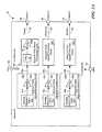
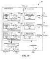
- an exemplary implementation of the sensor IC 20(from FIGS. 1A-1B ), shown here as current sensor IC 40 , includes the three sensing elements 22 a , 22 b and 22 c .
- the sensing elements 22 a , 22 b , 22 care part of magnetic field signal generating circuits 42 a , 42 b , 42 c , respectively.
- the sensing elements 22 a , 22 b , 22 csense magnetic fields associated with one or both of conduction paths 14 a , 14 b and produce respective sensing element output signals 44 a , 44 b , 44 c , e.g., voltage signals, proportional to the sensed magnetic fields.
- the magnetic field signal generating circuits 42 a , 42 b , 42 cmay contain various conventional circuits that operate collectively to generate magnetic field signal generating circuit output signals (or magnetic field signals) 46 a , 46 b , 46 c , respectively.
- each of the magnetic field signal generating circuits 42 a , 42 b and 42 cincludes at least an amplifier for amplifying the output signal of the sensing element 22 a , 22 b and 22 c , respectively.
- magnetic field signal generating circuit 42 aincludes amplifier 48 a to produce the magnetic field signal 46 a
- magnetic field signal generating circuit 42 bincludes amplifier 48 b to produce the magnetic field signal 46 b
- magnetic field signal generating circuit 42 cincludes amplifier 48 c to produce magnetic field signal 46 c.
- each circuit 42 a - 42 cmay include circuitry to implement dynamic offset cancellation. If the sensing elements 22 a - 22 c are Hall plates, a chopper stabilization circuit can be provided to minimize the offset voltage of the Hall plates and associated amplifiers 48 a - 48 c . Also, or alternatively, each circuit 42 a - 42 c may implement an offset adjustment feature, by which the magnetic field signal is centered within the power supply range of the sensor and/or a gain adjustment feature, by which the gain of the magnetic field signal is adjusted to maximize the peak-to-peak within the power supply range without causing clipping.
- the sensor device or IC 40also includes magnetic field signal processing circuits 50 a , 50 b , 50 c .
- the circuits 50 a - 50 ceach includes a respective low-pass filter 52 and output amplifier/buffer 54 , which process respective magnetic field signal 46 a , 46 b , 46 c to produce respective magnetic field signal processing circuitry output signals 56 , 60 , 58 .
- Output signals 56 , and 60are absolute measurement signals and output signal 58 is a measured difference measurement signal (or difference signal).
- the output signal 56 and output signal 60would be indicative of phase current magnitude and neutral current magnitude (as shown), respectively, and the difference signal 58 would be indicative of a difference between the phase and neutral current magnitudes.
- the sensor device 40may be provided in the form of an IC containing a semiconductor substrate on which the various circuit elements are formed.
- the ICwould have at least one pin (terminal or lead) to correspond to each of: the VCC input or terminal 62 (to connect to an external power supply), GND terminal 64 (to connect to ground), and outputs including ‘output 1 ’ 66 , ‘output 2 ’ 68 and ‘output 3 ’ 70 .
- Outputs 66 , 70 , 68enable an external differential current sensor application such as a GFI circuit or other application to receive and make use of any one or more of the output signals 56 , 60 , 58 , respectively.
- VCC pin 62Power is supplied to the IC 40 through the VCC pin 62 , which is connected internally to the various subcircuits, as shown.
- a protection circuitrepresented here as a simple Zener diode 72 , is provided between the VCC pin 62 and ground for protection in the event that the supply pin is shorted to ground.
- the GND pin 64is connected internally to provide a ground connection for subcircuits of the sensor.
- Other circuitry, such as control and clock generation, for example,has been eliminated from the figure for purposes of simplification.
- the three sensing elements 22 a - 22 care used to obtain the same measurements as device 40 from FIG. 2A .
- the device 80differs from device 40 in that the device 80 provides a sum or total signal instead of signals corresponding to separate absolute measurements at its outputs.
- the device 80includes only two signal paths, one to produce a total signal 82 at a “new” output 1 84 (which replaces outputs 66 and 70 on device 40 ).
- the device 80includes a magnetic field signal generating circuit 86 , which includes sensing elements 22 a and 22 b , as well as a summer element 88 to combine the sensing elements outputs 44 a and 44 b (from sensing elements 22 a and 22 b , respectively) to produce a total sensing element output 90 .
- the circuit 86also includes an amplifier, shown as amplifier 48 a ′, which provides an output 92 .
- the device 80further includes a magnetic field signal processing circuit, shown as circuitry 50 a ′, which processes the output 92 to produce the total signal 82 .
- the difference signal pathis the same as device 40 , that is, it uses magnetic field signal generating circuit 42 c and magnetic field signal processing circuitry 50 c to produce difference signal 58 at output 68 .
- the total signal 82would be indicative of a total (or sum) of phase and neutral current magnitudes.
- a sensing device or IC 100like device 80 , provides two outputs corresponding to total and difference signals, but utilizes only sensing elements 22 a and 22 b to do so.
- a magnetic field signal generating circuit 102 in device 100replaces the circuit 42 c in device 80 .
- Circuit 102includes sensing elements 22 a and 22 b , and a subtractor (or difference) element 104 to take the difference between the outputs 44 a and 44 b from sensing elements 22 a and 22 b , respectively, and to provide the result as a difference output 106 .
- circuit 102includes an amplifier, shown here as amplifier 48 c ′, to amplify the difference output 106 .
- the corresponding output signal(provided at the output of circuit 50 c and made available at output 68 ) is shown here as difference signal 108 .
- the difference signal 108indicates a difference determined from the measurements of sensing elements 22 a and 22 b , not one that is based on the measurement of sensing element 22 c (like the difference signal 58 in FIG. 2B ).
- That difference signalmay be produced/computed by SE 1 22 a and SE 2 22 b , or measured by a “middle” sensing element positioned to measure current of both conductors, like SE 3 22 c .
- the circuitry to support the total current signalthat is, the signal path from sum element 76 through output 84 ), could be eliminated.
- the signal paths for (and including) the sensing elements SE 1 22 a and SE 2 22 be.g., as shown in FIGS.
- the ACS710 current sensorincludes internal circuitry and pins to detect overcurrent conditions, as well as provides a zero current reference pin and filter pin to which a user can connect an external capacitor to set device bandwidth.
- exemplary functionssuch as those available in the ACS761 current monitor IC, which incorporates circuitry and pins to support various levels of fault protection, including overpower, overcurrent and short circuit faults (with an external high-side FET gate driver for disabling the load), and other features (e.g., valid power indicator), could also be included.
- the signal paths of the sensor IC embodiments of FIGS. 2A-2Dcan be implemented in the analog or in the digital domain.
- sensing element 22 asenses the magnetic field associated with the phase current in conduction path 14 a and sensing element 22 b senses the magnetic field associated with the neutral current in conduction path 14 b .
- sensing element 22 bsenses the magnetic field associated with the neutral current in conduction path 14 b .
- the sensing element 22 csenses the magnetic fields associated with both the phase current flowing in conduction path 14 a and the neutral current flowing in conduction path 14 b .
- the sensing element 22 cdetects that difference (the amount of current that was diverted from the conduction path 14 b ).
- that current difference or lossis determined by taking the difference between the outputs of sensing elements 22 a and 22 b , as described earlier.
- the sensor device or ICcan be implemented to provide a total signal indicative of the total of the phase and neutral current magnitudes, or alternatively, separate signals indicative of the absolute current in each conduction path, also as described earlier with respect to FIGS. 2A-2C .
- FIG. 3illustrates a simple ground fault interrupter circuit 110 that employs the differential current sensor 10 (from FIG. 1A ).
- the differential current sensor 10is coupled to current conductors or wires 112 a and 112 b , which are connected to a load 114 .
- the current conductor 112 acarries the phase current from a power source to the load 114 .
- the current conductor 112 bcarries the neutral current from the load 114 .
- the sensor 10measures the difference between the amount of neutral current and the amount of phase current and provides a difference signal, difference signal 116 (generated by the internal sensing IC, e.g., as depicted in FIGS.
- the GFI circuit 110also includes a trip circuit 122 (or “circuit breaker”), which actuates a set of switches, for example, switches 124 a , 124 b (coupled to the conductors/wires 112 a , 112 b , respectively) in response to the trip signal 120 . That is, the trip signal 120 is used to trigger the trip circuit 122 to open the switches 124 (and thus disconnect the power source).
- the trip circuit 122may be implemented with any suitable electromechanical trip device, e.g., a trip coil.
- FIG. 3is a simplified depiction of a GFI application and is not intended to show the physical layout of signals at the board or system level.
- the current conductors 112 a , 112 bwould be appropriately routed to the current sensor 10 (via the circuit board traces) so that I 1 and I 2 flow into and out of the current sensor 10 in the same direction as described earlier (and not in opposite directions as shown in FIG. 3 ).
- An alternative GFI design in which I 1 and I 2 flow into and out of the current sensor in opposite directionscould also be used, but such a design would need to take into account that SE 3 would sense twice the magnetic field.
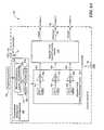
- a sensor IC with an integrated coil driver circuit, sensor IC 130can include the internal magnetic field signal generating and processing circuitry from the sensing device, for example, sensor device 80 (from FIG. 2B ), indicated here as sensor 132 .
- sensor device 80from FIG. 2B
- the sensor 132would produce the total current signal 82 and difference signal 58 .
- the new sensor 130has two outputs, output 84 and output 122 .
- the output 84receives the total current signal 82 .
- the sensor 130also includes a coil driver 134 and sensor/driver interface logic 136 to interface the sensor 132 to the coil driver 134 .
- the sensor/driver interface logic 136receives the difference signal 58 and, in response to that signal, produces a coil driver input signal 138 .
- the coil driver 134In response to the coil driver input signal 138 , the coil driver 134 generates an appropriate drive signal 140 .
- sensor 130could replace sensor device 20 inside differential current sensor 10 to enable that sensor to directly trigger the trip circuit 122 with the new sensor's drive signal 140 .
- This more integrated solutioneliminates the need for the drive circuit 118 in the GFI circuit 110 .
- the circuitry of sensor 132could include that shown in FIG. 2C , or alternatively, the circuitry of sensor IC 40 shown in FIG. 2A with outputs 66 and 70 replacing output 84 or the circuitry of sensor IC 104 shown in FIG. 2D with total current signal 82 and output 84 omitted.
- FIGS. 5A and 5Bshow partial side views of sensor IC and conduction paths, indicated by reference numerals 150 and 152 .
- FIG. 5Aillustrates a perfect alignment of sensing elements 22 a , 22 b and 22 c relative to conduction paths 14 a , 14 b .
- FIG. 5Billustrates a case of misalignment. The outline of the IC is omitted, as the misalignment may occur as the result of sensing element spacing on the die or positioning the IC within a sensor package, as discussed above. Other sources of error that would lead to misalignment may include manufacturing tolerances in placement or the width of the conduction paths 14 a and 14 b . Referring to FIG.
- the sensing element 22 cwill not be centered between the two conduction paths 14 a and 14 b as shown. Instead, and referring to FIG. 5B , the sensing elements 22 a , 22 b and 22 c will be offset to one side, e.g., offset 154 , as shown.
- the middle (differential current) sensingcan be implemented with an arrangement of two or more sensing elements. The arrangement is centered relative to the two conduction paths 14 a , 14 b when the sensor IC is properly aligned with the conduction paths, as is depicted in FIGS. 5C-5E .
- the direction of misalignment, should it occur,is indicated by arrow 158 .
- sensing element 22 cand additional sensing elements 22 d and 22 e located on either side of sensing element 22 c .
- the sensing elements 22 c - 22 emay be provided in a linearly spaced arrangement as shown in FIG. 5D or non-linearly spaced arrangement.
- An example of a non-linearly spaced arrangement of the sensing elementsis illustrated in FIG. 5E .
- FIG. 5Eshows sensing elements of uniform size, the size of the sensing elements can vary within a given arrangement.
- the sensing elements 22 a and 22 b(from FIGS. 5A-5B ) have been omitted from the illustrations of FIGS.
- the measurement of the difference between the currents flowing in the conduction paths provided by the middle sensing element 22 cmay be adjusted in a number of different ways.
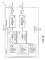
- the electronics for the sensor ICcan be adjusted by means of electronic trimming. For example, and referring to FIGS. 6A-6B , the sensor IC, shown as current sensor IC 160 in FIG. 6A or current sensor IC 160 ′ in FIG.
- the block 162can include some type of memory element(s) 164 , a digital-to-analog converter 166 to convert digital contents of the memory element(s) 164 to analog format, if necessary, and a programmable control logic block 168 to provide a control interface to the magnetic field signal generating circuits, for example, magnetic field signal generating circuits 42 a , 42 b , 42 c (from FIG. 2A ).
- the memory element(s) 164can be registers, RAM, one time programmable or re-programmable ROM or other nonvolatile memory.
- the memory element(s) 164are coupled to the D/A converter 166 via a memory-to-D/A line 170 and the D/A converter 166 is coupled to the control logic block 168 via a D/A-to-control line 172 .
- the output of the control logic block 168is provided to the magnetic field signal generating circuits 42 a - 42 c , shown collectively as magnetic field signal generating circuits 174 , via a control logic output line 176 .
- the magnetic field signal processing circuits 50 a - 50 c from FIG. 2Aare shown collectively as magnetic field signal processing circuits 178 .
- Other features of the sensor IC 160are the same as shown in FIG. 2A .
- the control logic output line from block 162is provided to magnetic field signal generating circuits 174 ′, which differs from the magnetic field signal generating circuits 174 in FIG. 6A in that the circuits 174 ′ also includes magnetic field signal generating circuitry for sensing elements 22 d and 22 e .
- circuits 174 ′includes such circuits for sensing elements 22 d and 22 e .
- Sensing element 22 dprovides an output 44 d that is amplified by an amplifier 48 d , which provides a signal 46 d to magnetic signal processing circuits 178 .
- Sensing element 22 eprovides an output 44 e that is amplified by an amplifier 48 e , which provides a signal 46 e to the magnetic field signal processing circuits 178 .
- the magnetic field signal generating circuitry that produces the signals 46 c , 46 d and 46 eis indicated collectively as block 179 .
- the line 176 ′is provided to the magnetic field signal generating circuits 174 ′, e.g., at least the portion shown as block 179 (as shown in FIG. 6B ).
- misalignment compensation or correctioncan be accomplished with digital correction to the signal paths using parameters programmed into the sensor chip. For example, in one possible implementation, testing can determine the offset (e.g., offset 154 from FIG. 5B ) and program the block 162 to add or subtract that offset from the sensing element output 44 c . Thus, and referring to FIG. 6A , the offset value would be provided to the memory element(s) 164 and applied to the appropriate sensing element circuitry via the control logic block 168 .
- the adjustment block 162may be used to select the most accurate of the measurements of the sensing elements, 22 c , 22 d , 22 e or a mathematical arrangement (or combination) of the three sensing elements' measurements to use as the difference measurement.
- An example of a simple mathematical arrangementwould be to average the measurements for two adjacent sensing elements, for example, (A+B)/2 to arrive at a value between A and B, where A denotes the measurement associated with sensing element 22 d and B denotes the measurement associated with sensing element 22 c (for example).
- the sensing elements of interest for the mathematical averagingcould be sensing element 22 e and sensing element 22 c instead of sensing elements 22 d and 22 c .
- the sensing elements 22 d , 22 c and 22 emay be non-linearly spaced (for example, as illustrated in FIG. 5E ) to allow other mathematical combinations of interest or positions of interest based on assembly tolerances of the differential current sensor. It may be possible to utilize sensing elements 22 a , 22 c and 22 b in the same manner (as sensing elements 22 d , 22 c and 22 e , respectively), but such usage would be application specific.
- differential current sensing elementsit is also possible to use some other number of differential current sensing elements than the three shown in FIGS. 5C-5D and 6 B, for example, but not limited to: 2, 4, 5, 6, 7 and 8 sensing elements.
- the number of the sensing elementswill be practically limited by required die area and test time to find the best combination to be used in the final product or programming of the individual part. The adjustment could be performed before or after installation, depending on the type of package that is used.
- the block 179(shown in dashed lines) is a programmable or configurable block. That is, it contains various programmable on-chip features (not shown) that enable the desired configuration, e.g., selection and/or combination of signals 44 c , 44 d and 44 e , and appropriate selection of any magnetic field signal generating circuitry and signal paths necessary to provide a single output from block 179 . That single output, which may appear at a selected one of lines 46 c , 46 d and 46 e , is provided to the corresponding magnetic field signal processing circuit (in block 178 ), e.g., circuit 50 c shown in FIG. 2A , for generating the difference signal 58 at output 68 . That difference signal that appears at output 68 will have been compensated for misalignment offset based on selections applied under the control of programmable misalignment offset adjustment block 162 .
- the desired configuratione.g., selection and/or combination of signals 44 c , 44 d and 44 e
- FIGS. 6A and 6Binclude sensing elements 22 a , 22 b and corresponding signal paths, those sensing elements and signal paths may be eliminated.
- the magnetic field signal generating and processing circuits associated with the sensing elements 22 a , 22 bmay be replaced with those shown in FIG. 2B (to provide a single “total current” output instead of separate phase and neutral current outputs).
- sensing element 22 c(or 22 c , 22 d , 22 e , if additional sensing elements 22 d and 22 e are also used) to be implemented as a standard Si Hall plate instead of one made of a more sensitive material, as was mentioned earlier.
- sensing element 22 cor 22 c , 22 d , 22 e , if additional sensing elements 22 d and 22 e are also used
- the concept of using multiple sensing elements and selecting the best one or a mathematical combination to provide a value based on the middle sensing element(s), i.e., sensing element 22 c or, alternatively, multiple sensing elements, e.g., sensing elements 22 c , 22 d and 22 ecould also be applied to implementations in which any one or more of the sensing elements are made of materials other than Si.
- the sensor IC depicted in FIGS. 1A-1B and 2 A- 2 Cprovides information at its outputs corresponding to absolute or total values (in addition to difference values) for a measured parameter, such as current, it is a multi-purpose device that can be used in a variety of different applications. For example, as discussed above, it may be used to measure current in current divider applications or current measurement applications that require redundancy. The device would also be suitable for use in applications that sense magnetic field to measure displacement.
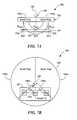
- FIGS. 7A-7Bshow different views of an example angle sensing structure 180 .
- the structure 180includes a permanent magnet 182 shown as a two-pole magnet having a South pole 184 a and a North pole 184 b .
- the sensor IC 20Positioned in proximity to the magnet 82 is the sensor IC 20 .
- the sensor IC 20can determine a rotation angle ⁇ 186 of the two-pole magnet 182 about an axis of rotation 188 .
- sensing element 22 ais used to generate a sine signal and sensing element 22 b is used to generate a cosine signal for the rotation angle 186 at outputs 66 and 70 , respectively. From the two outputs, a value indicative of the rotation angle 186 can be determined.
- the rotation angle 186 that is measuredcan be in the range of 0 to 360 degrees.
- the sensor IC 20may be stationary and the magnet 182 attached to a rotating shaft (rotor) near the sensor IC 20 .
- the third (or middle) sensing element 22 cis used to detect sensor-to-magnet misalignment.
- SE 1 22 a and SE 2 22 bhave to be positioned on two lines (SE 1 on line 189 a and SE 2 on line 189 b ) that are at 90 degrees to each other and pass through point 188 .
- sensing by SE 1 22 aprovides a first sine waveform
- sensing by SE 2 22 bprovides a second sine waveform phase shifted by 90 degrees from the first sine waveform (that is, a cosine waveform).
- sensing by SE 3 22 cprovides a sine waveform that is phased shifted from the first sine waveform by a phase angle that is less than 90 degrees.
- the positioning of SE 3 22 cis such that it results in a sine waveform that is phase shifted by a phase angle of 45 degrees. More generally, the phase angle may be within a range of values, for example, 30 to 60 degrees.
- SE 3 22 cneed not be located on a line formed by SE 1 22 a and SE 2 22 b , and that the distance from SE 3 22 c to SE 1 22 a need not be equal to the distance from SE 3 22 c to SE 2 22 b .
- prior angle sensing deviceswith only two sensing elements and capable of producing only a sine signal and a cosine signal, the amplitudes and phases of both signals needed to be examined and corrected, if necessary, in cases of misalignment.
- IC 20provides an arrangement of three sensing elements, with SE 3 22 c being located between SE 1 22 a and SE 2 22 b (e.g., at a mid-point between SE 1 22 a and SE 2 22 b as illustrated in earlier figures and illustrated again in FIGS. 7A and 7B ), the IC 20 produces three signals. Referring back to FIG. 2A , the IC 20 generates a sine signal at output 66 , a cosine signal at output 70 and a signal produced from sensing by SE 3 22 c and made available at output 68 . Consequently, the signal based in sensing by SE 3 22 c provides additional information that can be used to determine and correct for misalignment.
- the signal information from all three sensing elementsis used to define an error function or equation.
- the error functionprovides an error value “X” as being equal to a mathematical combination of the signal values (that is, amplitudes) of the three signals.
- An application employing the error functionmay be implemented to recognize X as a first, “minimal error” value for an alignment condition and as a different second value (e.g., not equal to, or greater than, the first value) for a misalignment condition.
- the goal of an application that uses an error function based on the sensing of SE 1 22 a , SE 2 22 b and SE 3 22 c , as described above,is to minimize the error function (and thus the amount of misalignment) for a desired level of accuracy in angle determination. It can do so through some form of correction.
- the correctionmay be implemented electronically or with a mechanical adjustment of the sensor/magnet assembly for optimal alignment, resulting in improved angle accuracy.
- FIGS. 8A-8Bshow exemplary angle measurement devices 190 (FIG. 8 A) and 190 ′ ( FIG. 8B ) that utilize the output of the angle sensor to determine a rotation angle value.
- the angle measurement device 190(or 190 ′) includes an angle sensor, for example, the sensor IC 20 from FIG. 2A , and a processing unit 192 ( FIG. 8A ) or 192 ′ ( FIG. 8B ).
- the signal processing unit 192 (or 192 ′)performs the angle calculation. It combines the two absolute output signals from the angle sensor 20 into one digital output signal.
- the processing unit 192 (or 192 ′)provides a digital output, although it could be designed to provide an analog output instead.
- Output signals provided at the sensor's outputs 66 and 70are sampled and then converted into the digital domain by an Analog-to-Digital Converter (ADC) 196 ( FIG. 8A ) or 196 ′ ( FIG. 8B ).
- a processor (or microcontroller) 198 ( FIG. 8A ) or 198 ′ ( FIG. 8B )receives digital representations of the sensor output signals, shown as ADC outputs 200 a , 200 b , and uses software shown as an angle determiner 202 ( FIG. 8A ) or 202 ′ ( FIG. 8B ) to determine an angle value from the ADC outputs 200 a , 200 b .
- CORDICCOordinate Rotation DIgital Computer
- arctangentor “arctan” trigonometric function calculation for angle value determination.
- Other algorithms that can determine the angle value from the sine and cosine signalsmay be used as well.
- Clock and control signalsare provided to the ADC 196 (or 196 ′) and the processor 198 (or 198 ′) by a clock generation and control circuit 203 . Once the angle is determined, it is represented as an angle value at an output 204 ( FIG. 8A ) or 204 ′ ( FIG. 8B ) that is accessible by an external controller or user (not shown).
- the output signal provided at the sensor's output 68(from FIG. 2A ), shown here as output signal 194 c , provides information that is used to compensate for the sensor-to-magnet misalignment electronically.
- the output signal 194 cis sampled and then converted into the digital domain by the ADC 196 ′.
- the processor 198 ′receives the digital representation of that sensor output signal, shown as ADC output 200 c , along with the ADC outputs 200 a and 200 b , and uses software shown as misalignment corrector 205 to compute the error function and to compensate for misalignment indicated by the error function.
- misalignment corrector 205uses software shown as misalignment corrector 205 to compute the error function and to compensate for misalignment indicated by the error function.
- the misalignment corrector 205includes an error determiner (or error function block) 206 and a corrector (or correction block) 207 .
- the error function block 206defines an error function that combines the signal values 200 a , 200 b and 200 c , and performs the error function to generate an error value 208 indicative of alignment or misalignment.
- the error value 208is provided to the correction block 207 , which determines an appropriate correction based on the error value 208 and provides correction information 209 to the angle determiner 202 ′.
- the angle determiner 202 ′uses the correction information to produce the angle value 204 ′. That is, the angle determiner 202 ′ produces an angle value that has been corrected for any misalignment detected by the misalignment corrector 205 .
- the misalignment corrector 205receives the signal values 200 a , 220 b and 200 c , and uses those signal values to compute the error value (according to a predetermined error function, as discussed above) to detect misalignment.
- the misalignment corrector 205then applies a correction to the output produced by the angle determiner 202 ′ (or provides correction information 209 to angle determiner 202 ′, which incorporates the correction information in its angle determination, as discussed above), thus minimizing error on the angle value 204 ′.
- the correction block 207could be configured to compute a correction value “on-the-fly.” Other implementations are possible as well.
- the correction block 207could be provided with a lookup table of predetermined correction values and configured to perform a lookup to provide appropriate correction values for computed error values.
- the processcould include an electronic misalignment detection and mechanical misalignment correction.
- the misalignment detectioncould be performed “externally” using a device like the programming device 163 shown in FIG. 6 .
- the usercould rotate the magnet (again, for example, one half turn or one full turn) and examine the sensor output signals 194 a , 194 b and 194 c to detect misalignment.
- Thiscould be done, for example, by using software running on the programming device 163 .
- the software of programming device 163would include an error function block (like error function block 206 of the processing unit 192 ′ of FIG. 8B ) to provide an error value based on a mathematical combination of the signals 194 a - 194 c .
- the userWhen the error value indicates misalignment, the user would then correct the misalignment mechanically, that is, by adjusting the magnet-to-sensor position in that user's system and possibly repeating this routine (e.g., by performing the magnet rotation followed by the error function computation, for each magnet-to-sensor position) until minimal error function corresponding to a desired degree of alignment is achieved.
- the angle sensore.g., IC 20
- outputs 194 a and 194 bcould be processed by a device such as processing unit 192 (FIG. 8 BA) for angle determination.
- An electronic misalignment correction of the type provided by a device like processing unit 192 ′ ( FIG. 8B )would not be necessary.
- IC 20hardware and/or software to implement the error function block may be included in IC 20 . If IC 20 is modified to include this functionality, then the functionality need not be provided elsewhere, for example, in misalignment corrector 205 (of FIG. 8B ) for applications that utilize electronic misalignment correction or other devices such as programming device 163 for applications that utilize a mechanical misalignment correction.
- the permanent magnet 182 illustrated in FIGS. 7A-7Bhas only one pair of North/South poles, the above-described approach to misalignment detection and correction is also applicable to sensing applications that utilize magnets with more than one pole pair.
- the use of a magnet with more than one pole pairis possible as long as the positions of SE 1 22 a and SE 2 22 b are such that they generate 90 degrees out-of-phase signals when the sensor 20 is aligned with the magnet.
- the sensor IC 20 and processing unit 192may be packaged in separate integrated circuit chips. Alternatively, devices can be manufactured that incorporate both sensor and processing electronics on the same chip.
- FIG. 9Another type of displacement measurement that could be performed by the sensor IC 20 presented in FIG. 1A-1B and FIG. 2A is linear displacement.
- the sensor ICwould be particularly useful for a linear displacement measurement application requiring redundancy.
- the sensing elements 22 a , 22 b , 22 c of sensor IC 20would sense the magnetic field associated with the linear movement of the bar magnet.
- the middle sensing element 22 cis now performing the same function as the other sensing elements 22 a , 22 b , that is, it is making an absolute (rather than a differential) measurement.
- the path of linear motionis along an axis indicated by an arrow 216 . That movement or displacement, which could be bidirectional or unidirectional, would be represented as a linear voltage value (proportional to the magnetic field) at corresponding outputs 66 , 70 , 68 . In a redundancy application, only one of the outputs 66 , 68 , 70 would be used at any given time.
- the application(or alternatively, the IC itself) could be configured with a failover type scheme to switch from the output currently in use to one of the unused outputs, e.g., when an error has occurred.
- the IC 20 and magnet 212would be part of a larger system (not shown), for example, a magnet and sensor IC/coil assembly (of a linear motor or other linear motion system).
- a magnet and sensor IC/coil assemblyof a linear motor or other linear motion system.
- the flux generated by the energized coilinteracts with flux generated by the magnet, which causes the magnet to move either in one direction or the opposite direction depending on the polarity of the coil flux.
- the sensor device described abovecan be used in any consumer, industrial or automotive application requiring the measurement of a small difference between two similar currents, and is therefore not limited to GFI applications. Also, since it can be implemented to include two individual magnetic field sensing elements to measure the absolute incoming currents, the sensor device can be used for redundancy applications if the same current is applied to both conduction paths. The sensor device can also be used for linear position applications requiring redundancy, as well as for 360 degree angle sensing. In the angle sensing application, two sensing elements can provide sine and cosine signals for the angle determination, and the third sensing element can be used to improve magnet-to-sensor alignment (and therefore total angle accuracy), as discussed above.
- the arrangementIn absence of any misalignment, the arrangement would be centered relative to the external target (that is, the source of the magnetic flux to be sensed by the SEs, whether that source is a pair of current conduction paths or magnet(s)) for a zero field indication. If misalignment between the sensor and such target should occur, a non-zero field would be indicated by the arrangement.
- One of the misalignment offset compensation schemes discussed earliercould then be used to “zero” the result provided by the arrangement so that the sensor output signal (such as a difference signal for a GFI application current sensor, as described above, or a linear position sensor's output signal, for example) is more accurate.
- the sensor circuitrycan be modified to provide a sensor IC 220 that includes a self-test block or circuit (also referred to as a built-in self-test or “BIST” circuit) 222 , coupled to subcircuits via an interconnect 224 , to provide self-test functionality.
- the self-test circuit 222could have at least one input line 226 and output line 230 and corresponding terminals 228 and 232 , respectively, for exchanging diagnostics test information with an external device (e.g., a controller).
- a command or request for diagnostics testcould be provided to the self-test circuit 222 on the input line 226 (via terminal 228 ) and results could be returned on the output line 230 (via terminal 232 ).
- the self-test circuit 222in response to a command on input line 226 , would enable self-test of at least some or all of the various subcircuits (such as circuits 42 a - 42 c and circuits 50 a - 50 c ).
- the self-test circuitis shown as part of a sensor IC like that shown in FIG. 2A , it is applicable to other described embodiments as well. This type of circuitry would provide added safety, thus making its inclusion particularly attractive for GFI applications.
- the self-test circuit 222can be implemented in a number of different ways, according to design and application requirements. For example, it could be implemented to incorporate self-test features described in U.S. Patent Application Publication No. US2010/0211347, of application Ser. No. 12/706,318 entitled “Circuits and Methods for Generating a Self-Test of a Magnetic Field Sensor,” filed Feb. 16, 2010 and assigned to Allegro Microsystems, Inc., the assignee of the subject application.
- the self-test circuit 222can be implemented to include a self-test current conductor for generating a self-test magnetic field and circuitry to process the measured self-test magnetic field to generate a diagnostic and/or other signal(s), as discussed in the aforementioned patent application.
- the use of other types of self-test/BIST mechanismsis contemplated as well.
- each sensing elementmay be a device made of a IV type semiconductor material such as Si or Ge, or a III-V type semiconductor material like GaAs or an Indium compound.
Landscapes
- Physics & Mathematics (AREA)
- General Physics & Mathematics (AREA)
- Measuring Instrument Details And Bridges, And Automatic Balancing Devices (AREA)
Abstract
Description
Claims (51)
Priority Applications (5)
| Application Number | Priority Date | Filing Date | Title |
|---|---|---|---|
| US13/439,094US9081041B2 (en) | 2012-04-04 | 2012-04-04 | High accuracy differential current sensor for applications like ground fault interrupters |
| KR1020147028166AKR101950710B1 (en) | 2012-04-04 | 2013-03-21 | High accuracy differential current sensor for applications like ground fault interrupters |
| PCT/US2013/033248WO2013151792A1 (en) | 2012-04-04 | 2013-03-21 | High accuracy differential current sensor for applications like ground fault interrupters |
| EP13713708.9AEP2815244B1 (en) | 2012-04-04 | 2013-03-21 | High accuracy differential current sensor for applications like ground fault interrupters |
| EP20183925.5AEP3742180A1 (en) | 2012-04-04 | 2013-03-21 | High accuracy differential current sensor for applications like ground fault interrupters |
Applications Claiming Priority (1)
| Application Number | Priority Date | Filing Date | Title |
|---|---|---|---|
| US13/439,094US9081041B2 (en) | 2012-04-04 | 2012-04-04 | High accuracy differential current sensor for applications like ground fault interrupters |
Publications (2)
| Publication Number | Publication Date |
|---|---|
| US20130265041A1 US20130265041A1 (en) | 2013-10-10 |
| US9081041B2true US9081041B2 (en) | 2015-07-14 |
Family
ID=49291793
Family Applications (1)
| Application Number | Title | Priority Date | Filing Date |
|---|---|---|---|
| US13/439,094Active2032-11-01US9081041B2 (en) | 2012-04-04 | 2012-04-04 | High accuracy differential current sensor for applications like ground fault interrupters |
Country Status (1)
| Country | Link |
|---|---|
| US (1) | US9081041B2 (en) |
Cited By (43)
| Publication number | Priority date | Publication date | Assignee | Title |
|---|---|---|---|---|
| US20160291069A1 (en)* | 2013-09-30 | 2016-10-06 | Airbus Defence And Space Limited | Phase angle measurement using residue number system analogue-to-digital conversion |
| US20180088159A1 (en)* | 2016-09-29 | 2018-03-29 | U.S. Army Research Laboratory Attn: Rdrl-Loc-I | Non-contact multi-phase cable sensor |
| US20180188293A1 (en)* | 2016-12-30 | 2018-07-05 | Texas Instruments Incorporated | Magnetic field-based current measurement |
| US20180231618A1 (en)* | 2017-02-16 | 2018-08-16 | Tdk Corporation | Magnetic sensor apparatus |
| US20180306843A1 (en)* | 2017-04-25 | 2018-10-25 | Allegro Microsystems, Llc | Systems and Methods For Current Sensing |
| US10310028B2 (en) | 2017-05-26 | 2019-06-04 | Allegro Microsystems, Llc | Coil actuated pressure sensor |
| US10324141B2 (en) | 2017-05-26 | 2019-06-18 | Allegro Microsystems, Llc | Packages for coil actuated position sensors |
| US10436607B2 (en) | 2016-09-16 | 2019-10-08 | Apple Inc. | Motion sensing using hall voltage signals |
| US10557873B2 (en) | 2017-07-19 | 2020-02-11 | Allegro Microsystems, Llc | Systems and methods for closed loop current sensing |
| US20200088546A1 (en)* | 2018-09-14 | 2020-03-19 | Allegro Microsystems, Llc | Angular magnetic field sensor and rotating target with stray field immunity |
| US10641842B2 (en) | 2017-05-26 | 2020-05-05 | Allegro Microsystems, Llc | Targets for coil actuated position sensors |
| US10670672B2 (en) | 2013-07-19 | 2020-06-02 | Allegro Microsystems, Llc | Method and apparatus for magnetic sensor producing a changing magnetic field |
| US10712372B2 (en)* | 2017-10-16 | 2020-07-14 | Schneider Electric Industries Sas | Current measurement device, manufacturing method, protection module and differential circuit breaker including such a device |
| US10761120B2 (en) | 2017-02-17 | 2020-09-01 | Allegro Microsystems, Llc | Current sensor system |
| US10823586B2 (en) | 2018-12-26 | 2020-11-03 | Allegro Microsystems, Llc | Magnetic field sensor having unequally spaced magnetic field sensing elements |
| US10837943B2 (en) | 2017-05-26 | 2020-11-17 | Allegro Microsystems, Llc | Magnetic field sensor with error calculation |
| US10866117B2 (en) | 2018-03-01 | 2020-12-15 | Allegro Microsystems, Llc | Magnetic field influence during rotation movement of magnetic target |
| US10884031B2 (en) | 2018-08-17 | 2021-01-05 | Allegro Microsystems, Llc | Current sensor system |
| US10955306B2 (en) | 2019-04-22 | 2021-03-23 | Allegro Microsystems, Llc | Coil actuated pressure sensor and deformable substrate |
| US10996289B2 (en) | 2017-05-26 | 2021-05-04 | Allegro Microsystems, Llc | Coil actuated position sensor with reflected magnetic field |
| US11061084B2 (en) | 2019-03-07 | 2021-07-13 | Allegro Microsystems, Llc | Coil actuated pressure sensor and deflectable substrate |
| US11143719B2 (en)* | 2017-10-06 | 2021-10-12 | Murata Manufacturing Co., Ltd. | Magnetic sensor and current sensor |
| US11150273B2 (en) | 2020-01-17 | 2021-10-19 | Allegro Microsystems, Llc | Current sensor integrated circuits |
| US11226382B2 (en) | 2020-04-07 | 2022-01-18 | Allegro Microsystems, Llc | Current sensor system |
| US11237020B2 (en) | 2019-11-14 | 2022-02-01 | Allegro Microsystems, Llc | Magnetic field sensor having two rows of magnetic field sensing elements for measuring an angle of rotation of a magnet |
| US11262422B2 (en) | 2020-05-08 | 2022-03-01 | Allegro Microsystems, Llc | Stray-field-immune coil-activated position sensor |
| US11280637B2 (en) | 2019-11-14 | 2022-03-22 | Allegro Microsystems, Llc | High performance magnetic angle sensor |
| US11307054B2 (en) | 2014-10-31 | 2022-04-19 | Allegro Microsystems, Llc | Magnetic field sensor providing a movement detector |
| US11320466B1 (en) | 2020-10-29 | 2022-05-03 | Allegro Microsystems, Llc | Differential current sensor |
| US11385075B2 (en) | 2020-02-21 | 2022-07-12 | Allegro Microsystems, Llc | Orientation independent magnetic field sensor |
| US11402409B1 (en) | 2021-03-22 | 2022-08-02 | Allegro Microsystems, Llc | Differential current sensor package |
| US11428755B2 (en) | 2017-05-26 | 2022-08-30 | Allegro Microsystems, Llc | Coil actuated sensor with sensitivity detection |
| US11493361B2 (en) | 2021-02-26 | 2022-11-08 | Allegro Microsystems, Llc | Stray field immune coil-activated sensor |
| US11561112B2 (en) | 2020-03-13 | 2023-01-24 | Allegro Microsystems, Llc | Current sensor having stray field immunity |
| US11566918B2 (en) | 2020-08-13 | 2023-01-31 | The United States Of America As Represented By The Secretary Of The Army | Non contact power meter independent of placement of field sensors around the cable |
| US11578997B1 (en) | 2021-08-24 | 2023-02-14 | Allegro Microsystems, Llc | Angle sensor using eddy currents |
| US11656250B2 (en) | 2021-09-07 | 2023-05-23 | Allegro Microsystems, Llc | Current sensor system |
| US11892476B2 (en) | 2022-02-15 | 2024-02-06 | Allegro Microsystems, Llc | Current sensor package |
| US11940470B2 (en) | 2022-05-31 | 2024-03-26 | Allegro Microsystems, Llc | Current sensor system |
| US11994541B2 (en) | 2022-04-15 | 2024-05-28 | Allegro Microsystems, Llc | Current sensor assemblies for low currents |
| US12112865B2 (en) | 2022-03-15 | 2024-10-08 | Allegro Microsystems, Llc | Multiple branch bus bar for coreless current sensing application |
| US12306214B2 (en)* | 2022-12-15 | 2025-05-20 | Infineon Technologies Ag | Adjustable sensitivity ranges for magnetic field sensors |
| US12352786B2 (en) | 2021-09-07 | 2025-07-08 | Allegro Microsystems, Llc | Current sensor system |
Families Citing this family (40)
| Publication number | Priority date | Publication date | Assignee | Title |
|---|---|---|---|---|
| US9222992B2 (en)* | 2008-12-18 | 2015-12-29 | Infineon Technologies Ag | Magnetic field current sensors |
| US8975889B2 (en) | 2011-01-24 | 2015-03-10 | Infineon Technologies Ag | Current difference sensors, systems and methods |
| US8963536B2 (en) | 2011-04-14 | 2015-02-24 | Infineon Technologies Ag | Current sensors, systems and methods for sensing current in a conductor |
| US8896295B2 (en) | 2012-04-04 | 2014-11-25 | Allegro Microsystems, Llc | Magnetic field sensor having multiple sensing elements and a programmable misalignment adjustment device for misalignment detection and correction in current sensing and other applications |
| US9606190B2 (en)* | 2012-12-21 | 2017-03-28 | Allegro Microsystems, Llc | Magnetic field sensor arrangements and associated methods |
| US9417295B2 (en) | 2012-12-21 | 2016-08-16 | Allegro Microsystems, Llc | Circuits and methods for processing signals generated by a circular vertical hall (CVH) sensing element in the presence of a multi-pole magnet |
| US9164155B2 (en) | 2013-01-29 | 2015-10-20 | Infineon Technologies Ag | Systems and methods for offset reduction in sensor devices and systems |
| WO2015033541A1 (en)* | 2013-09-05 | 2015-03-12 | 旭化成エレクトロニクス株式会社 | Current sensor |
| US9605983B2 (en) | 2014-06-09 | 2017-03-28 | Infineon Technologies Ag | Sensor device and sensor arrangement |
| DE102014008173B4 (en) | 2014-06-10 | 2022-08-11 | Tdk-Micronas Gmbh | magnetic field measuring device |
| US9823168B2 (en) | 2014-06-27 | 2017-11-21 | Infineon Technologies Ag | Auto tire localization systems and methods utilizing a TPMS angular position index |
| CN104297549A (en)* | 2014-09-11 | 2015-01-21 | 国家电网公司 | A flexible clamp current tester |
| US9455653B1 (en) | 2015-03-05 | 2016-09-27 | Ford Global Technologies, Llc | Reliable current sensing for inverter-controlled electronic machine |
| JP6618370B2 (en)* | 2015-03-05 | 2019-12-11 | エイブリック株式会社 | Magnetic sensor circuit |
| JP6268128B2 (en)* | 2015-07-17 | 2018-01-24 | 矢崎総業株式会社 | Switch box and overcurrent prevention method |
| US9733280B2 (en)* | 2015-09-08 | 2017-08-15 | Infineon Technologies Ag | Balancing an eddy current effect and a skin effect on a magnetic sensor using die paddle notches |
| FR3050278B1 (en)* | 2016-04-15 | 2018-03-30 | Saft | METHOD FOR DETERMINING THE VALUE OF PARAMETERS RELATING TO THE STATUS OF AN BATTERY BATTERY BATTERY BATTERY AND ELECTRONIC BATTERY MANAGEMENT SYSTEM |
| CN109154629B (en)* | 2016-05-16 | 2021-01-05 | 日立汽车系统株式会社 | Current detection device and power conversion device provided with same |
| WO2018080516A1 (en)* | 2016-10-28 | 2018-05-03 | Hewlett-Packard Development Company, L.P. | Current monitor circuit |
| EP3367110B1 (en)* | 2017-02-24 | 2024-04-17 | Monolithic Power Systems, Inc. | Current sensing system and current sensing method |
| US10718794B2 (en)* | 2018-06-20 | 2020-07-21 | Allegro Microsystems, Llc | Current sensor with power calculation |
| US10739411B2 (en)* | 2018-06-04 | 2020-08-11 | Ford Global Technologies, Llc | Power electronic test automation circuit |
| US11671029B2 (en) | 2018-07-07 | 2023-06-06 | Intelesol, Llc | AC to DC converters |
| US11581725B2 (en) | 2018-07-07 | 2023-02-14 | Intelesol, Llc | Solid-state power interrupters |
| US11349296B2 (en) | 2018-10-01 | 2022-05-31 | Intelesol, Llc | Solid-state circuit interrupters |
| US10834792B2 (en) | 2018-12-17 | 2020-11-10 | Intelesol, Llc | AC-driven light-emitting diode systems |
| JP7166205B2 (en)* | 2019-03-12 | 2022-11-07 | 株式会社東芝 | semiconductor integrated circuit |
| US11551899B2 (en) | 2019-05-18 | 2023-01-10 | Amber Semiconductor, Inc. | Intelligent circuit breakers with solid-state bidirectional switches |
| US12253545B2 (en) | 2019-11-24 | 2025-03-18 | Purdue Research Foundation | High accuracy non-invasive current sensor system |
| FR3103902B1 (en)* | 2019-11-28 | 2021-12-17 | Aptiv Tech Ltd | Device and method for measuring electric current in a cable |
| US11721508B2 (en) | 2019-12-06 | 2023-08-08 | Amber Semiconductor, Inc. | Solid-state ground-fault circuit interrupter |
| JP7289782B2 (en)* | 2019-12-19 | 2023-06-12 | 株式会社東芝 | current detector |
| US11467188B2 (en) | 2020-02-25 | 2022-10-11 | Infineon Technologies Ag | Current sensor for improved functional safety |
| EP4197086A4 (en) | 2020-08-11 | 2024-09-04 | Amber Semiconductor, Inc. | INTELLIGENT ENERGY SOURCE MONITORING AND SELECTION CONTROL SYSTEM |
| KR102562009B1 (en)* | 2021-06-28 | 2023-08-01 | 주식회사 루텍 | High Current Measurement Device |
| US12113525B2 (en) | 2021-09-30 | 2024-10-08 | Amber Semiconductor, Inc. | Intelligent electrical switches |
| US11733025B2 (en)* | 2021-10-14 | 2023-08-22 | Allegro Microsystems, Llc | Dynamic offset and amplitude tracker |
| US12348028B2 (en) | 2021-10-22 | 2025-07-01 | Amber Semiconductor, Inc. | Multi-output programmable power manager |
| US12362646B2 (en) | 2022-01-26 | 2025-07-15 | Amber Semiconductor, Inc. | Controlling AC power to inductive loads |
| US20240241157A1 (en)* | 2023-01-17 | 2024-07-18 | Littelfuse, Inc. | Current sensor with diagnostic feature |
Citations (45)
| Publication number | Priority date | Publication date | Assignee | Title |
|---|---|---|---|---|
| US4101829A (en)* | 1976-07-06 | 1978-07-18 | Gte International, Inc. | Differential current detector |
| US4602212A (en)* | 1982-06-14 | 1986-07-22 | Sumitomo Metal Industries, Ltd. | Method and apparatus including a flux leakage and eddy current sensor for detecting surface flaws in metal products |
| US5442221A (en)* | 1992-05-27 | 1995-08-15 | Schlumberger Industries, S.A. | Hall effect sensor |
| US6040690A (en)* | 1995-01-18 | 2000-03-21 | Horstmann Timers & Controls Limited | Electricity measurement using two conductors |
| US6291907B1 (en)* | 1997-10-23 | 2001-09-18 | Analog Devices, Inc. | Magnetically coupled signal isolator using a faraday shielded MR or GMR receiving element |
| US6310470B1 (en)* | 1997-04-19 | 2001-10-30 | Lust Antriebstechnik Gmbh | Method and device for measuring the difference in magnetic field strength with magnetoresistive sensors |
| US6509732B1 (en) | 2000-05-01 | 2003-01-21 | Honeywell International Inc. | Enhanced methods for sensing positions of an actuator moving longitudinally |
| US6762897B1 (en) | 1997-09-08 | 2004-07-13 | Kabushiki Kaisha Yaskawa Denki | Magnetic encoder apparatus |
| US20050073293A1 (en) | 2003-10-01 | 2005-04-07 | Hastings Jerome K. | Integrated anti-differential current sensing system |
| US20050156587A1 (en)* | 2004-01-16 | 2005-07-21 | Fieldmetrics Inc. | Current sensor |
| US20050275399A1 (en) | 2004-06-14 | 2005-12-15 | Denso Corporation | Method and apparatus for sensing angle of rotation |
| US20060213952A1 (en)* | 2003-09-22 | 2006-09-28 | Dukane Corporation | Multiple probe power systems and methods for ultrasonic welding |
| US7166807B2 (en) | 2003-08-26 | 2007-01-23 | Allegro Microsystems, Inc. | Current sensor |
| US20070200564A1 (en)* | 2006-02-28 | 2007-08-30 | Mario Motz | Magnetic Field Sensor, Sensor Comprising Same and Method for Manufacturing Same |
| US20080042644A1 (en) | 2006-08-17 | 2008-02-21 | Sl Corporation | Electronic Shift Lever Assembly |
| WO2008145600A1 (en) | 2007-06-01 | 2008-12-04 | Kem-O-Tek Italia Srl | Circuit for protection against the risk of electric shocks |
| US20080297158A1 (en) | 2007-05-31 | 2008-12-04 | Zircon Corporation | Gradiometric Directional Metal Detector |
| US7476816B2 (en) | 2003-08-26 | 2009-01-13 | Allegro Microsystems, Inc. | Current sensor |
| US7492149B2 (en) | 2002-05-28 | 2009-02-17 | Infineon Technologies Ag | Circuit configuration for processing a signal of a sensor and method of using the circuit configuration |
| US20090168280A1 (en)* | 2008-01-02 | 2009-07-02 | Ememory Technology Inc. | Electrostatic discharge avoiding circuit |
| US20090174395A1 (en) | 2008-01-04 | 2009-07-09 | Thomas Monica J | Methods and apparatus for angular position sensing using multiple quadrature signals from frequency independent sinusoids |
| US20090243606A1 (en)* | 2008-03-26 | 2009-10-01 | Austriamicrosystems Ag | Sensor Arrangement, Integrated Chip Component with the Sensor Arrangement, and Measurement Method |
| US20090315555A1 (en)* | 2008-06-22 | 2009-12-24 | Heger Charles E | Power cable magnetic field sensor |
| US20100007340A1 (en)* | 2008-07-14 | 2010-01-14 | Tdk Corporation | Angle detecting apparatus and angle detecting method |
| US7714570B2 (en) | 2006-06-21 | 2010-05-11 | Allegro Microsystems, Inc. | Methods and apparatus for an analog rotational sensor having magnetic sensor elements |
| US20100156394A1 (en)* | 2008-12-18 | 2010-06-24 | Infineon Technologies Ag | Magnetic field current sensors |
| US20100156397A1 (en)* | 2008-12-23 | 2010-06-24 | Hitoshi Yabusaki | Methods and apparatus for an angle sensor for a through shaft |
| US7759929B2 (en) | 2005-03-30 | 2010-07-20 | Austriamicrosystems Ag | System and method for determining an angle of rotation with cascade sensors |
| US20100211347A1 (en) | 2009-02-17 | 2010-08-19 | Allegro Microsystems, Inc. | Circuits and Methods for Generating a Self-Test of a Magnetic Field Sensor |
| US20110043197A1 (en) | 2007-10-25 | 2011-02-24 | Janez Trontelj | Method and Device for Contactless Sensing Rotation and Angular Position Using Orientation Tracking |
| US20110057649A1 (en)* | 2006-04-05 | 2011-03-10 | Minoru Yoshida | Method and its apparatus for detecting defects |
| US20110216452A1 (en)* | 2010-03-08 | 2011-09-08 | Pass & Seymour, Inc. | Protective device for an electrical supply facility |
| US20110221429A1 (en)* | 2010-03-09 | 2011-09-15 | Alps Green Devices Co., Ltd. | Current sensor |
| US20110316561A1 (en) | 2010-06-25 | 2011-12-29 | Keith Raynard Tinsley | Systems, methods, apparatus and computer readable mediums for use association with systems having interference |
| US20120098527A1 (en) | 2007-05-10 | 2012-04-26 | Cambridge Integrated Circuits Limited | Transducer |
| US20120126805A1 (en) | 2010-11-18 | 2012-05-24 | Infineon Technologies Ag | Current Sensor |
| US20120187943A1 (en)* | 2011-01-24 | 2012-07-26 | Udo Ausserlechner | Current difference sensors, systems and methods |
| US20120194175A1 (en) | 2011-02-01 | 2012-08-02 | Infineon Technologies Ag | Sensor |
| US20120194945A1 (en)* | 2011-02-02 | 2012-08-02 | Seagate Technology Llc | Compensation for cross-track deviation |
| US20120229131A1 (en)* | 2009-08-26 | 2012-09-13 | Panasonic Corporation | Magnetic field sensor, as well as magnetic field measurement method, power measurement device, and power measurement method using the same |
| US20130002857A1 (en) | 2011-06-30 | 2013-01-03 | Qualcomm Incorporated | Navigation in buildings with rectangular floor plan |
| US20130015843A1 (en) | 2011-07-13 | 2013-01-17 | Allegro Microsystems, Inc. | Current sensor with calibration for a current divider configuration |
| US20130020660A1 (en) | 2011-07-22 | 2013-01-24 | Allegro Microsystems, Inc. | Reinforced Isolation for Current Sensor with Magnetic Field Transducer |
| US20130265037A1 (en) | 2012-04-04 | 2013-10-10 | Allegro Microsystems, Inc. | Angle sensor with misalignment detection and correction |
| US20130265036A1 (en) | 2012-04-04 | 2013-10-10 | Allegro Microsystems, Inc. | Magnetic field sensor having multiple sensing elements for misalignment detection and correction in current sensing and other applications |
- 2012
- 2012-04-04USUS13/439,094patent/US9081041B2/enactiveActive
Patent Citations (48)
| Publication number | Priority date | Publication date | Assignee | Title |
|---|---|---|---|---|
| US4101829A (en)* | 1976-07-06 | 1978-07-18 | Gte International, Inc. | Differential current detector |
| US4602212A (en)* | 1982-06-14 | 1986-07-22 | Sumitomo Metal Industries, Ltd. | Method and apparatus including a flux leakage and eddy current sensor for detecting surface flaws in metal products |
| US5442221A (en)* | 1992-05-27 | 1995-08-15 | Schlumberger Industries, S.A. | Hall effect sensor |
| US6040690A (en)* | 1995-01-18 | 2000-03-21 | Horstmann Timers & Controls Limited | Electricity measurement using two conductors |
| US6310470B1 (en)* | 1997-04-19 | 2001-10-30 | Lust Antriebstechnik Gmbh | Method and device for measuring the difference in magnetic field strength with magnetoresistive sensors |
| US6762897B1 (en) | 1997-09-08 | 2004-07-13 | Kabushiki Kaisha Yaskawa Denki | Magnetic encoder apparatus |
| US6291907B1 (en)* | 1997-10-23 | 2001-09-18 | Analog Devices, Inc. | Magnetically coupled signal isolator using a faraday shielded MR or GMR receiving element |
| US6509732B1 (en) | 2000-05-01 | 2003-01-21 | Honeywell International Inc. | Enhanced methods for sensing positions of an actuator moving longitudinally |
| US7492149B2 (en) | 2002-05-28 | 2009-02-17 | Infineon Technologies Ag | Circuit configuration for processing a signal of a sensor and method of using the circuit configuration |
| US7166807B2 (en) | 2003-08-26 | 2007-01-23 | Allegro Microsystems, Inc. | Current sensor |
| US7476816B2 (en) | 2003-08-26 | 2009-01-13 | Allegro Microsystems, Inc. | Current sensor |
| US20060213952A1 (en)* | 2003-09-22 | 2006-09-28 | Dukane Corporation | Multiple probe power systems and methods for ultrasonic welding |
| US20050073293A1 (en) | 2003-10-01 | 2005-04-07 | Hastings Jerome K. | Integrated anti-differential current sensing system |
| US20050156587A1 (en)* | 2004-01-16 | 2005-07-21 | Fieldmetrics Inc. | Current sensor |
| US20050275399A1 (en) | 2004-06-14 | 2005-12-15 | Denso Corporation | Method and apparatus for sensing angle of rotation |
| US7759929B2 (en) | 2005-03-30 | 2010-07-20 | Austriamicrosystems Ag | System and method for determining an angle of rotation with cascade sensors |
| US20070200564A1 (en)* | 2006-02-28 | 2007-08-30 | Mario Motz | Magnetic Field Sensor, Sensor Comprising Same and Method for Manufacturing Same |
| US20110057649A1 (en)* | 2006-04-05 | 2011-03-10 | Minoru Yoshida | Method and its apparatus for detecting defects |
| US7714570B2 (en) | 2006-06-21 | 2010-05-11 | Allegro Microsystems, Inc. | Methods and apparatus for an analog rotational sensor having magnetic sensor elements |
| US7994774B2 (en) | 2006-06-21 | 2011-08-09 | Allegro Microsystems, Inc. | Methods and apparatus for an analog rotational sensor having magnetic sensor elements |
| US7911203B2 (en) | 2006-06-21 | 2011-03-22 | Allegro Microsystems, Inc. | Sensor having an analog processing module to generate a linear position output |
| US20080042644A1 (en) | 2006-08-17 | 2008-02-21 | Sl Corporation | Electronic Shift Lever Assembly |
| US20120098527A1 (en) | 2007-05-10 | 2012-04-26 | Cambridge Integrated Circuits Limited | Transducer |
| US20080297158A1 (en) | 2007-05-31 | 2008-12-04 | Zircon Corporation | Gradiometric Directional Metal Detector |
| WO2008145600A1 (en) | 2007-06-01 | 2008-12-04 | Kem-O-Tek Italia Srl | Circuit for protection against the risk of electric shocks |
| US20110043197A1 (en) | 2007-10-25 | 2011-02-24 | Janez Trontelj | Method and Device for Contactless Sensing Rotation and Angular Position Using Orientation Tracking |
| US20090168280A1 (en)* | 2008-01-02 | 2009-07-02 | Ememory Technology Inc. | Electrostatic discharge avoiding circuit |
| US8125216B2 (en) | 2008-01-04 | 2012-02-28 | Allegro Microsystems, Inc. | Methods and apparatus for angular position sensing using multiple quadrature signals |
| US20090174395A1 (en) | 2008-01-04 | 2009-07-09 | Thomas Monica J | Methods and apparatus for angular position sensing using multiple quadrature signals from frequency independent sinusoids |
| US20090243606A1 (en)* | 2008-03-26 | 2009-10-01 | Austriamicrosystems Ag | Sensor Arrangement, Integrated Chip Component with the Sensor Arrangement, and Measurement Method |
| US20090315555A1 (en)* | 2008-06-22 | 2009-12-24 | Heger Charles E | Power cable magnetic field sensor |
| US20100007340A1 (en)* | 2008-07-14 | 2010-01-14 | Tdk Corporation | Angle detecting apparatus and angle detecting method |
| US20100156394A1 (en)* | 2008-12-18 | 2010-06-24 | Infineon Technologies Ag | Magnetic field current sensors |
| US20100156397A1 (en)* | 2008-12-23 | 2010-06-24 | Hitoshi Yabusaki | Methods and apparatus for an angle sensor for a through shaft |
| US20100211347A1 (en) | 2009-02-17 | 2010-08-19 | Allegro Microsystems, Inc. | Circuits and Methods for Generating a Self-Test of a Magnetic Field Sensor |
| US20120229131A1 (en)* | 2009-08-26 | 2012-09-13 | Panasonic Corporation | Magnetic field sensor, as well as magnetic field measurement method, power measurement device, and power measurement method using the same |
| US20110216452A1 (en)* | 2010-03-08 | 2011-09-08 | Pass & Seymour, Inc. | Protective device for an electrical supply facility |
| US20110221429A1 (en)* | 2010-03-09 | 2011-09-15 | Alps Green Devices Co., Ltd. | Current sensor |
| US20110316561A1 (en) | 2010-06-25 | 2011-12-29 | Keith Raynard Tinsley | Systems, methods, apparatus and computer readable mediums for use association with systems having interference |
| US20120126805A1 (en) | 2010-11-18 | 2012-05-24 | Infineon Technologies Ag | Current Sensor |
| US20120187943A1 (en)* | 2011-01-24 | 2012-07-26 | Udo Ausserlechner | Current difference sensors, systems and methods |
| US20120194175A1 (en) | 2011-02-01 | 2012-08-02 | Infineon Technologies Ag | Sensor |
| US20120194945A1 (en)* | 2011-02-02 | 2012-08-02 | Seagate Technology Llc | Compensation for cross-track deviation |
| US20130002857A1 (en) | 2011-06-30 | 2013-01-03 | Qualcomm Incorporated | Navigation in buildings with rectangular floor plan |
| US20130015843A1 (en) | 2011-07-13 | 2013-01-17 | Allegro Microsystems, Inc. | Current sensor with calibration for a current divider configuration |
| US20130020660A1 (en) | 2011-07-22 | 2013-01-24 | Allegro Microsystems, Inc. | Reinforced Isolation for Current Sensor with Magnetic Field Transducer |
| US20130265037A1 (en) | 2012-04-04 | 2013-10-10 | Allegro Microsystems, Inc. | Angle sensor with misalignment detection and correction |
| US20130265036A1 (en) | 2012-04-04 | 2013-10-10 | Allegro Microsystems, Inc. | Magnetic field sensor having multiple sensing elements for misalignment detection and correction in current sensing and other applications |
Non-Patent Citations (24)
| Title |
|---|
| Allegro Datasheet ACS710, 120 kHz Bandwidth, High Voltage Isolation Current Sensor with Integrated Overcurrent Detection, 2007-2009,15 pages. |
| Allegro Datasheet ACS761ELF-20B, 12V High-Side Hot-Swap Hall Effect Based Current Monitor IC, 2008-2009, 14 pages. |
| Friedrich et al., U.S. Appl. No. 13/078,200, Entitled "Differential Magnetic Field Sensor Structure for Orientation Independent Measurement" filed Apr. 1, 2011, 64 Pages. |
| Friedrich et al., U.S. Appl. No. 13/439,074, Entitled "Magnetic Field Sensor Having Multiple Sensing Elements for Misalignment Detection and Correction in Current Sensing and Other Applications" filed Apr. 4, 2012, 62 Pages. |
| Friedrich et al., U.S. Appl. No. 13/439,082, Entitled "Angle Sensor With Misalignment Detection and Correction" filed Apr. 4, 2012, 62 Pages. |
| International Preliminary Report on Patentability dated Oct. 16, 2014 for PCT App. No. PCT/US2013/033248; 6 pages. |
| International Search Report dated Jul. 1, 2013, PCT/US2013/033248, 4 pages. |
| Maria Gabriella Masi et al: "A Self-Shielded Current Transducer for Power System Application", Applied Measurements for Power Systems (Amps), 2011 IEEE International Workshop on, IEEE, Sep. 28, 2011, pp. 43-47, DOI:10.1109/AMPS.2011.6090432, ISBN: 1-61284-946-1. |
| Maria Gabriella Masi, Lorenzo Peretto, Roberto Tinarelli, A Self-Shielded Current Transducer for Power System Application, IEEE, 2011, pp. 1-5. |
| Notice of Allowance dated Feb. 5, 2015 for U.S. Appl. No. 13/439,082;9pages. |
| Notice of Allowance dated Sep. 15, 2014 for U.S. Appl. No. 13/439,074; 7 pages. |
| Notification Concerning Transmittal of Copy of International Preliminary Report on Patentability (Chapter I of the Patent Cooperation Treaty) dated Jul. 1, 2013, PCT/US2013/033248, 1 page. |
| Office Action dated Feb. 13, 2014 for U.S. Appl. No. 13/439,082, filed Apr. 4, 2012, 25 pages. |
| Office Action dated Jul. 9, 2014 for U.S. Appl. No. 13/439,074, 14 pages. |
| Office Action dated Jul. 9, 2014 for U.S. Appl. No. 13/439,074; 14 pages. |
| Office Action dated Mar. 3, 2014 for U.S. Appl. No. 13/439,074, filed Apr. 4, 2012, 15 pages. |
| Office Action dated Oct. 8, 2014 for U.S. Appl. No. 13/439,082; 24 pages. |
| Response filed Mar. 31, 2014 to Office Action dated Mar. 3, 2013 for U.S. Appl. No. 13/439,074, filed Apr. 4, 2012, 10 pages. |
| Response to Office Action dated Feb. 13, 2014, U.S. Appl. No. 13/439,082, filed Apr. 4, 2012, 15 pages. |
| Response to Office Action filed Dec. 5, 2014 for U.S. Appl. No. 13/439,082; 12 pages. |
| Response to Office Action filed May 7, 2015 for European Application No. 13713708.9, 26 pages. |
| Response to Office Action filed on Aug. 19, 2014 for U.S. Appl. No. 13/439,074; 12 pages. |
| Response to Office Action filed on May 5, 2014 for U.S. Appl. No. 13/439,082; 13 pages. |
| Written Opinion of the International Searching Authority, PCT/US2013/033248 Jul. 1, 2013, 6 pages. |
Cited By (59)
| Publication number | Priority date | Publication date | Assignee | Title |
|---|---|---|---|---|
| US12061246B2 (en) | 2013-07-19 | 2024-08-13 | Allegro Microsystems, Llc | Method and apparatus for magnetic sensor producing a changing magnetic field |
| US10670672B2 (en) | 2013-07-19 | 2020-06-02 | Allegro Microsystems, Llc | Method and apparatus for magnetic sensor producing a changing magnetic field |
| US11313924B2 (en) | 2013-07-19 | 2022-04-26 | Allegro Microsystems, Llc | Method and apparatus for magnetic sensor producing a changing magnetic field |
| US9759754B2 (en)* | 2013-09-30 | 2017-09-12 | Airbus Defence And Space Limited | Phase angle measurement using residue number system analogue-to-digital conversion |
| US20160291069A1 (en)* | 2013-09-30 | 2016-10-06 | Airbus Defence And Space Limited | Phase angle measurement using residue number system analogue-to-digital conversion |
| US11307054B2 (en) | 2014-10-31 | 2022-04-19 | Allegro Microsystems, Llc | Magnetic field sensor providing a movement detector |
| US10859407B2 (en) | 2016-09-16 | 2020-12-08 | Apple Inc. | Motion sensing using hall voltage signals |
| US10436607B2 (en) | 2016-09-16 | 2019-10-08 | Apple Inc. | Motion sensing using hall voltage signals |
| US20180088159A1 (en)* | 2016-09-29 | 2018-03-29 | U.S. Army Research Laboratory Attn: Rdrl-Loc-I | Non-contact multi-phase cable sensor |
| US10775420B2 (en)* | 2016-09-29 | 2020-09-15 | The United States Of America As Represented By The Secretary Of The Army | Non-contact multi-phase cable sensor |
| US10598700B2 (en)* | 2016-12-30 | 2020-03-24 | Texas Instruments Incorporated | Magnetic field-based current measurement |
| US20180188293A1 (en)* | 2016-12-30 | 2018-07-05 | Texas Instruments Incorporated | Magnetic field-based current measurement |
| US20180231618A1 (en)* | 2017-02-16 | 2018-08-16 | Tdk Corporation | Magnetic sensor apparatus |
| US10761120B2 (en) | 2017-02-17 | 2020-09-01 | Allegro Microsystems, Llc | Current sensor system |
| US10908190B2 (en)* | 2017-04-25 | 2021-02-02 | Allegro Microsystems, Llc | Systems and methods for current sensing |
| US10481181B2 (en)* | 2017-04-25 | 2019-11-19 | Allegro Microsystems, Llc | Systems and methods for current sensing |
| US20180306843A1 (en)* | 2017-04-25 | 2018-10-25 | Allegro Microsystems, Llc | Systems and Methods For Current Sensing |
| US10324141B2 (en) | 2017-05-26 | 2019-06-18 | Allegro Microsystems, Llc | Packages for coil actuated position sensors |
| US11768256B2 (en) | 2017-05-26 | 2023-09-26 | Allegro Microsystems, Llc | Coil actuated sensor with sensitivity detection |
| US11428755B2 (en) | 2017-05-26 | 2022-08-30 | Allegro Microsystems, Llc | Coil actuated sensor with sensitivity detection |
| US10837943B2 (en) | 2017-05-26 | 2020-11-17 | Allegro Microsystems, Llc | Magnetic field sensor with error calculation |
| US10649042B2 (en) | 2017-05-26 | 2020-05-12 | Allegro Microsystems, Llc | Packages for coil actuated position sensors |
| US11320496B2 (en) | 2017-05-26 | 2022-05-03 | Allegro Microsystems, Llc | Targets for coil actuated position sensors |
| US10641842B2 (en) | 2017-05-26 | 2020-05-05 | Allegro Microsystems, Llc | Targets for coil actuated position sensors |
| US11073573B2 (en) | 2017-05-26 | 2021-07-27 | Allegro Microsystems, Llc | Packages for coil actuated position sensors |
| US10996289B2 (en) | 2017-05-26 | 2021-05-04 | Allegro Microsystems, Llc | Coil actuated position sensor with reflected magnetic field |
| US10310028B2 (en) | 2017-05-26 | 2019-06-04 | Allegro Microsystems, Llc | Coil actuated pressure sensor |
| US10557873B2 (en) | 2017-07-19 | 2020-02-11 | Allegro Microsystems, Llc | Systems and methods for closed loop current sensing |
| US11143719B2 (en)* | 2017-10-06 | 2021-10-12 | Murata Manufacturing Co., Ltd. | Magnetic sensor and current sensor |
| US10712372B2 (en)* | 2017-10-16 | 2020-07-14 | Schneider Electric Industries Sas | Current measurement device, manufacturing method, protection module and differential circuit breaker including such a device |
| US11313700B2 (en) | 2018-03-01 | 2022-04-26 | Allegro Microsystems, Llc | Magnetic field influence during rotation movement of magnetic target |
| US10866117B2 (en) | 2018-03-01 | 2020-12-15 | Allegro Microsystems, Llc | Magnetic field influence during rotation movement of magnetic target |
| US10884031B2 (en) | 2018-08-17 | 2021-01-05 | Allegro Microsystems, Llc | Current sensor system |
| US20200088546A1 (en)* | 2018-09-14 | 2020-03-19 | Allegro Microsystems, Llc | Angular magnetic field sensor and rotating target with stray field immunity |
| US11162815B2 (en)* | 2018-09-14 | 2021-11-02 | Allegro Microsystems, Llc | Angular magnetic field sensor and rotating target with stray field immunity |
| US10823586B2 (en) | 2018-12-26 | 2020-11-03 | Allegro Microsystems, Llc | Magnetic field sensor having unequally spaced magnetic field sensing elements |
| US11061084B2 (en) | 2019-03-07 | 2021-07-13 | Allegro Microsystems, Llc | Coil actuated pressure sensor and deflectable substrate |
| US10955306B2 (en) | 2019-04-22 | 2021-03-23 | Allegro Microsystems, Llc | Coil actuated pressure sensor and deformable substrate |
| US11280637B2 (en) | 2019-11-14 | 2022-03-22 | Allegro Microsystems, Llc | High performance magnetic angle sensor |
| US11237020B2 (en) | 2019-11-14 | 2022-02-01 | Allegro Microsystems, Llc | Magnetic field sensor having two rows of magnetic field sensing elements for measuring an angle of rotation of a magnet |
| US11150273B2 (en) | 2020-01-17 | 2021-10-19 | Allegro Microsystems, Llc | Current sensor integrated circuits |
| US11519939B2 (en) | 2020-01-17 | 2022-12-06 | Allegro Microsystems, Llc | Current sensor integrated circuits |
| US11385075B2 (en) | 2020-02-21 | 2022-07-12 | Allegro Microsystems, Llc | Orientation independent magnetic field sensor |
| US11561112B2 (en) | 2020-03-13 | 2023-01-24 | Allegro Microsystems, Llc | Current sensor having stray field immunity |
| US11226382B2 (en) | 2020-04-07 | 2022-01-18 | Allegro Microsystems, Llc | Current sensor system |
| US11262422B2 (en) | 2020-05-08 | 2022-03-01 | Allegro Microsystems, Llc | Stray-field-immune coil-activated position sensor |
| US11566918B2 (en) | 2020-08-13 | 2023-01-31 | The United States Of America As Represented By The Secretary Of The Army | Non contact power meter independent of placement of field sensors around the cable |
| US11320466B1 (en) | 2020-10-29 | 2022-05-03 | Allegro Microsystems, Llc | Differential current sensor |
| US11493361B2 (en) | 2021-02-26 | 2022-11-08 | Allegro Microsystems, Llc | Stray field immune coil-activated sensor |
| US11402409B1 (en) | 2021-03-22 | 2022-08-02 | Allegro Microsystems, Llc | Differential current sensor package |
| US11578997B1 (en) | 2021-08-24 | 2023-02-14 | Allegro Microsystems, Llc | Angle sensor using eddy currents |
| US11656250B2 (en) | 2021-09-07 | 2023-05-23 | Allegro Microsystems, Llc | Current sensor system |
| US12352786B2 (en) | 2021-09-07 | 2025-07-08 | Allegro Microsystems, Llc | Current sensor system |
| US11892476B2 (en) | 2022-02-15 | 2024-02-06 | Allegro Microsystems, Llc | Current sensor package |
| US12112865B2 (en) | 2022-03-15 | 2024-10-08 | Allegro Microsystems, Llc | Multiple branch bus bar for coreless current sensing application |
| US11994541B2 (en) | 2022-04-15 | 2024-05-28 | Allegro Microsystems, Llc | Current sensor assemblies for low currents |
| US12235294B2 (en) | 2022-04-15 | 2025-02-25 | Allegro MicroSystem, LLC | Current sensor assemblies for low currents |
| US11940470B2 (en) | 2022-05-31 | 2024-03-26 | Allegro Microsystems, Llc | Current sensor system |
| US12306214B2 (en)* | 2022-12-15 | 2025-05-20 | Infineon Technologies Ag | Adjustable sensitivity ranges for magnetic field sensors |
Also Published As
| Publication number | Publication date |
|---|---|
| US20130265041A1 (en) | 2013-10-10 |
Similar Documents
| Publication | Publication Date | Title |
|---|---|---|
| US9081041B2 (en) | High accuracy differential current sensor for applications like ground fault interrupters | |
| US8896295B2 (en) | Magnetic field sensor having multiple sensing elements and a programmable misalignment adjustment device for misalignment detection and correction in current sensing and other applications | |
| US9007054B2 (en) | Angle sensor with misalignment detection and correction | |
| EP2815244B1 (en) | High accuracy differential current sensor for applications like ground fault interrupters | |
| JP6033529B2 (en) | Detection device and current sensor | |
| US10578679B2 (en) | Magnetic field sensors having virtual signals | |
| EP3325989B1 (en) | Methods and apparatus for trimming a magnetic field sensor | |
| US10502589B2 (en) | XMR angle sensor arrangement with safety mechanism and method for monitoring the same | |
| US9851221B2 (en) | Hall sensor insensitive to external magnetic fields | |
| EP3123188A1 (en) | Circuits and methods for self-calibrating or self-testing a magnetic field sensor using phase discrimination | |
| WO2014105318A2 (en) | Methods and apparatus for a current sensor having fault detection and self test functionality | |
| US11555832B2 (en) | Integrated shunt and magnetic field current sensor | |
| WO2011141969A1 (en) | Magnetic field angle measurement device and rotation angle measurement apparatus using same | |
| US11946774B2 (en) | Position sensor and method for position sensing and diagnostic | |
| CN114424070A (en) | Differential signal current sensor | |
| CN115066621B (en) | Terminal shields for current sensors and circuit breakers | |
| US11231304B2 (en) | Magnetic field sensor and magnetic field sensing method | |
| US11953395B2 (en) | Magnetic field differential linear torque sensor | |
| US12282075B2 (en) | Sensor package and system | |
| JP2014181981A (en) | Current sensor | |
| EP3779487B1 (en) | Assembly and method for determining the strength of a magnetic stray field | |
| US11047926B2 (en) | Magnetic sensor | |
| US20250306134A1 (en) | Passive frequency compensation with coil pairs | |
| US20220043034A1 (en) | Current sensor |
Legal Events
| Date | Code | Title | Description |
|---|---|---|---|
| AS | Assignment | Owner name:ALLEGRO MICROSYSTEMS, INC., MASSACHUSETTS Free format text:ASSIGNMENT OF ASSIGNORS INTEREST;ASSIGNORS:FRIEDRICH, ANDREAS P.;FOLETTO, ANDREA;SCHELLER, P. KARL;AND OTHERS;SIGNING DATES FROM 20120328 TO 20120330;REEL/FRAME:027995/0202 | |
| AS | Assignment | Owner name:ALLEGRO MICROSYSTEMS, LLC, MASSACHUSETTS Free format text:CONVERSION AND NAME CHANGE;ASSIGNOR:ALLEGRO MICROSYSTEMS, INC.;REEL/FRAME:030426/0178 Effective date:20130321 | |
| AS | Assignment | Owner name:ALLEGRO MICROSYSTEMS, LLC, MASSACHUSETTS Free format text:ASSIGNMENT OF ASSIGNORS INTEREST;ASSIGNOR:ALLEGRO MICROSYSTEMS EUROPE LIMITED;REEL/FRAME:034171/0492 Effective date:20141107 | |
| STCF | Information on status: patent grant | Free format text:PATENTED CASE | |
| CC | Certificate of correction | ||
| MAFP | Maintenance fee payment | Free format text:PAYMENT OF MAINTENANCE FEE, 4TH YEAR, LARGE ENTITY (ORIGINAL EVENT CODE: M1551) Year of fee payment:4 | |
| AS | Assignment | Owner name:MIZUHO BANK LTD., AS COLLATERAL AGENT, NEW YORK Free format text:PATENT SECURITY AGREEMENT;ASSIGNOR:ALLEGRO MICROSYSTEMS, LLC;REEL/FRAME:053957/0620 Effective date:20200930 Owner name:CREDIT SUISSE AG, CAYMAN ISLANDS BRANCH, AS COLLATERAL AGENT, NEW YORK Free format text:PATENT SECURITY AGREEMENT;ASSIGNOR:ALLEGRO MICROSYSTEMS, LLC;REEL/FRAME:053957/0874 Effective date:20200930 | |
| MAFP | Maintenance fee payment | Free format text:PAYMENT OF MAINTENANCE FEE, 8TH YEAR, LARGE ENTITY (ORIGINAL EVENT CODE: M1552); ENTITY STATUS OF PATENT OWNER: LARGE ENTITY Year of fee payment:8 | |
| AS | Assignment | Owner name:MORGAN STANLEY SENIOR FUNDING, INC., AS THE COLLATERAL AGENT, MARYLAND Free format text:PATENT SECURITY AGREEMENT;ASSIGNOR:ALLEGRO MICROSYSTEMS, LLC;REEL/FRAME:064068/0459 Effective date:20230621 Owner name:ALLEGRO MICROSYSTEMS, LLC, NEW HAMPSHIRE Free format text:RELEASE OF SECURITY INTEREST IN PATENTS (R/F 053957/0620);ASSIGNOR:MIZUHO BANK, LTD., AS COLLATERAL AGENT;REEL/FRAME:064068/0360 Effective date:20230621 | |
| AS | Assignment | Owner name:ALLEGRO MICROSYSTEMS, LLC, NEW HAMPSHIRE Free format text:RELEASE OF SECURITY INTEREST IN PATENTS AT REEL 053957/FRAME 0874;ASSIGNOR:CREDIT SUISSE AG, CAYMAN ISLANDS BRANCH, AS COLLATERAL AGENT;REEL/FRAME:065420/0572 Effective date:20231031 |