US9076926B2 - Gallium and nitrogen containing trilateral configuration for optical devices - Google Patents
Gallium and nitrogen containing trilateral configuration for optical devicesDownload PDFInfo
- Publication number
- US9076926B2 US9076926B2US14/181,386US201414181386AUS9076926B2US 9076926 B2US9076926 B2US 9076926B2US 201414181386 AUS201414181386 AUS 201414181386AUS 9076926 B2US9076926 B2US 9076926B2
- Authority
- US
- United States
- Prior art keywords
- triangular facet
- height
- optical device
- lamp
- chip
- Prior art date
- Legal status (The legal status is an assumption and is not a legal conclusion. Google has not performed a legal analysis and makes no representation as to the accuracy of the status listed.)
- Active
Links
Images


Classifications
- H01L33/24—
- H—ELECTRICITY
- H10—SEMICONDUCTOR DEVICES; ELECTRIC SOLID-STATE DEVICES NOT OTHERWISE PROVIDED FOR
- H10H—INORGANIC LIGHT-EMITTING SEMICONDUCTOR DEVICES HAVING POTENTIAL BARRIERS
- H10H20/00—Individual inorganic light-emitting semiconductor devices having potential barriers, e.g. light-emitting diodes [LED]
- H10H20/80—Constructional details
- H10H20/81—Bodies
- H10H20/819—Bodies characterised by their shape, e.g. curved or truncated substrates
- H10H20/821—Bodies characterised by their shape, e.g. curved or truncated substrates of the light-emitting regions, e.g. non-planar junctions
- H01L33/0095—
- H01L33/20—
- H01L33/32—
- H—ELECTRICITY
- H10—SEMICONDUCTOR DEVICES; ELECTRIC SOLID-STATE DEVICES NOT OTHERWISE PROVIDED FOR
- H10H—INORGANIC LIGHT-EMITTING SEMICONDUCTOR DEVICES HAVING POTENTIAL BARRIERS
- H10H20/00—Individual inorganic light-emitting semiconductor devices having potential barriers, e.g. light-emitting diodes [LED]
- H10H20/01—Manufacture or treatment
- H—ELECTRICITY
- H10—SEMICONDUCTOR DEVICES; ELECTRIC SOLID-STATE DEVICES NOT OTHERWISE PROVIDED FOR
- H10H—INORGANIC LIGHT-EMITTING SEMICONDUCTOR DEVICES HAVING POTENTIAL BARRIERS
- H10H20/00—Individual inorganic light-emitting semiconductor devices having potential barriers, e.g. light-emitting diodes [LED]
- H10H20/80—Constructional details
- H10H20/81—Bodies
- H10H20/819—Bodies characterised by their shape, e.g. curved or truncated substrates
- H—ELECTRICITY
- H10—SEMICONDUCTOR DEVICES; ELECTRIC SOLID-STATE DEVICES NOT OTHERWISE PROVIDED FOR
- H10H—INORGANIC LIGHT-EMITTING SEMICONDUCTOR DEVICES HAVING POTENTIAL BARRIERS
- H10H20/00—Individual inorganic light-emitting semiconductor devices having potential barriers, e.g. light-emitting diodes [LED]
- H10H20/80—Constructional details
- H10H20/81—Bodies
- H10H20/822—Materials of the light-emitting regions
- H10H20/824—Materials of the light-emitting regions comprising only Group III-V materials, e.g. GaP
- H10H20/825—Materials of the light-emitting regions comprising only Group III-V materials, e.g. GaP containing nitrogen, e.g. GaN
Definitions
- embodiments of the disclosureinclude techniques for manufacturing optical devices, such as light emitting diodes (LEDs) using a separation process of thick gallium and nitrogen containing substrate members, such as GaN configured in polar, non-polar or semi-polar crystalline orientations or others.
- the gallium and nitrogen containing substrateis configured in a trilateral shape.
- the starting materialscan include polar gallium nitride containing materials.
- Embodiments of the disclosurecan be applied to applications such as white lighting, multi-colored lighting, general illumination, decorative lighting, automotive and aircraft lamps, street lights, lighting for plant growth, indicator lights, lighting for flat panel displays, other optoelectronic devices, and the like.
- Solid state lighting techniquesare known. Solid state lighting relies upon semiconductor materials to produce light emitting diodes. At first, red LEDs were demonstrated and introduced into commerce. Red LEDs use Aluminum Indium Gallium Phosphide or AlInGaP semiconductor materials. Most recently, Shuji Nakamura pioneered the use of InGaN materials to produce LEDs emitting light in the blue color range for blue LEDs. High intensity UV, blue, and green LEDs based on GaN have been proposed and even demonstrated with some success. Efficiencies have typically been highest in the UV-violet, dropping off as the emission wavelength increases to blue or green. Unfortunately, achieving high intensity, high-efficiency GaN-based green LEDs has been particularly problematic. Additionally, GaN based LEDs have been costly and difficult to produce on a wide-scale in an efficient manner. Although highly successful, solid state lighting techniques must be improved for full exploitation of their potential.
- the present advancesprovide a method of shaping a gallium and nitrogen containing substrate structure.
- the methodincludes providing a gallium and nitrogen containing substrate having a front region and a back region.
- the backside regioncomprises a plurality of p-type regions.
- the methodfurther includes forming n-type regions, which can be formed within the front region or the back region.
- the methodalso includes subjecting a first street region between at least a first portion of a first die and a second die provided on the front region to at least a first saw process configured using a rotating blade structure having a tip region extending from a base region.
- the tip regionis characterized by an angle of about 65 degrees (other angles are possible as well) and less to cause formation of a first trench region within the street region.
- the angle for the tip regioncan be larger as well.
- the first trench regionhas a corresponding angle of about 65 degrees and less.
- the methodalso includes subjecting a second street region between at least a second portion of the first die and the second die provided on the front region to at least a second saw process configured using rotating blade structure having a tip region extending from a base region.
- the tip regionis characterized by an angle of about 65 degrees and less to cause formation of a second trench region within the street region.
- the second trench regionhas a corresponding angle of about 65 degrees and less.
- the methodadditionally includes subjecting a third street region between at least a third portion of the first die and the second die provided on the front region to at least a third saw process configured using a rotating blade structure having a tip region extending from a base region.
- the tip regionis characterized by an angle of about 65 degrees and less to cause formation of a third trench region within the street region.
- the third trench regionhas a corresponding angle of about 65 degrees and less.
- the methodalso includes removing a chip having a first exposed region from a portion of the first trench region, second exposed region from a portion of the second trench region, and a third exposed region from a portion of the third trench region.
- the first exposed region, the second exposed region, and the third exposed regionform a tetragonal shaped structure or an extruded tetragonal shaped structure.
- a lateral region of the substrateis electrically coupled to n-type and p-type contacts.
- the present advancesprovide an optical device.
- the deviceincludes a gallium and nitrogen containing substrate material.
- the devicealso includes a selected active region area of less than 65 microns square formed overlying the substrate.
- the selected active region areacan be greater than 65 micron square.
- the active region areacan be greater than 65000 microns square as well.
- the devicehas an extraction efficiency characterized by a maximum emission region for the selected active region area substantially free from orthogonal angles.
- the present advancesprovide a method of separating small gallium and nitrogen containing chips from a substrate structure.
- the methodincludes providing a patterned substrate comprising a backside region.
- the patterned substrateincludes a plurality of chips. Each of the chips has a backside surface region.
- the methodalso includes coupling the backside region of the substrate to a polymeric tape substrate to hold the patterned substrate on the tape substrate.
- the methodincludes subjecting the patterned substrate to a saw process to partially cut between at least two of the chips from the patterned substrate.
- the saw processis configured to cause a sheer force such that one or more the chips can detach from the tape substrate if the blade penetrates through an entirety of a thickness of the substrate.
- the methodadditionally includes removing the partially cut patterned substrate attached to the polymeric tape from the saw process.
- the methodalso includes breaking the patterned substrate to detach the chip.
- the present advancesprovide an optical device.
- the deviceincludes a gallium and nitrogen containing substrate structure comprising a base region and at least six sides excluding the base region configured in a non-orthogonal spatial manner to the base.
- the devicealso includes an active region configured to one or more mirror structures to cause a selective emission of electromagnetic radiation.
- the present apparatus and methodcan be manufactured using conventional materials and/or methods according to one of ordinary skill in the art.
- the present advancesprovide for a method for singulation of thick c-plane GaN wafers into a trilateral-shaped LED chips defined by sidewalls.
- the sidewallsare characterized by an orientation of approximately 10-1-1.
- the m-planeis a natural break plane, which easily cleaves, in the case of c-plane GaN wafers, and therefore, a singulation process involving breaking exclusively or predominately along a set of m-plane orientations will have a higher yield than a process involving breaking along a-plane orientations.
- the present advancesprovide for trilateral pyramid shaped chips characterized by improved light extraction when compared to conventional square- or rectangle-shaped chips, due to an increase in the per-pass probability of escape of in-plane emission arising from a decrease in the probability of total internal reflection at the sidewalls.
- the trilateral shaped chipis configured using conventional saw and scribe techniques.
- FIG. 1depicts a method of a simulation method for shaped chip
- FIG. 2is an illustration of a simulation method for a conventional cubic chip
- FIGS. 3 and 4are illustrations of conventional and present shaped chip
- FIGS. 5 and 6are illustrations of a conventional square chip.
- FIGS. 7 and 8are illustrations of a triangular chip
- FIGS. 9 and 10are illustrations modeling a tetragon chip
- FIG. 11is an illustration of a pyramid shaped chip
- FIGS. 12 and 13are illustrations of effects of loss for shaped chips
- FIGS. 14 through 16are illustrations of light extraction and impact on chip shape geometry
- FIG. 17is a diagram illustrating shaped device with a large radiation emitting surface
- FIG. 18is a diagram illustrating a shaped LED device where electrical contacts are positioned at the bottom
- FIG. 19A and FIG. 19Bdepict variations in chip shape geometry and the corresponding impact on light extraction.
- FIG. 20is a diagram illustrating a method of shaping a substrate structure containing gallium and nitrogen material.
- embodiments of the disclosuresinclude techniques for manufacturing optical devices, such as light emitting diodes (LEDs) using a separation process of thick gallium and nitrogen containing substrate members, such as GaN configured in non-polar or semi-polar crystalline orientations or others.
- LEDslight emitting diodes
- the present disclosureprovides tetragonal shaped chips with non-orthogonal sidewalls.
- the starting materialscan include polar gallium nitride containing materials, and others.
- the embodimentscan be applied to applications such as white lighting, multi-colored lighting, general illumination, decorative lighting, automotive and aircraft lamps, street lights, lighting for plant growth, indicator lights, lighting for flat panel displays, other optoelectronic devices, and the like.
- Light extraction strategieshave historically relied on three-dimensional chip shaping with non-orthogonal chip sidewalls, as described in “High-power truncated-inverted-pyramid (AlxGa1-x)0.5In0.5P/GaP light emitting diodes exhibiting >50% external quantum efficiency”, Krames et al., Appl. Phys. Lett. vol. 75, No. 16, 18 Oct. 1999, which is incorporated by reference herein for all purposes.
- Three-dimensional shaping approacheshave the disadvantage in that they are difficult to scale up in light output. That is, to generate more light from a single chip, the chip generally must be made larger in size. Making these three-dimensional chips larger must either result in the use of thicker substrate wafers, or a decrease in the aspect ratio of the chip. Thicker substrates are typically not feasible from a cost standpoint. In addition, absorption losses will often increase. On the other hand, if the aspect ratio is not preserved, the light extraction efficiency is greatly diminished as a result of mirror loss and/or increased absorption by the substrate.
- the present disclosureprovides a design (e.g., the rectangular parallel-piped) having improved light extraction characteristics. That is, the present device and related methods provides at least three spatial dimensions and also provides for a scattering surface opposite a reflector contact.
- the present deviceshave high efficiency at high current density.
- the devicesmay be employed in small chips in arrays. These two factors allows for ‘three dimensional’ chip designs with a favorable (near 1:1) aspect ratio while still emitting more light per chip. This is of course because the design and method scales current density instead of active region area. This opens up the possibility for high light output per chip while still using reasonable substrate wafer thicknesses.
- Three-dimensional shaped structures with non-orthogonal sidewallssuch as the truncated inverted pyramid chip or the ATON or NOTA chip have been employed previously.
- these chipsemploy a non-native substrate (e.g., SiC for ATON devices) or a wafer fused substrate which serves as the light extracting medium, as described in “Hexagonal pyramid shaped light-emitting diodes based on ZnO and GaN direct wafer bonding”, Mural et al, Appl. Phys. Lett. 89, 171116 (2006).
- the present shaped chipsdo not involve shaping of any material other than GaN.
- for the equilateral triangle base) Because the critical angle for GaN (n ⁇ 2.56) to silicone (n1.41) is approximately 32°, the equilateral triangle is particularly advantageous. This is not to say that all light is emitted for tetragonal shaped chips on the first or second reflection, because the vector defined by both the horizontal and vertical components must be incident at an angle below ⁇ c.
- both the horizontal and vertical components of a raycan of course be less than ⁇ c but the angle of incidence greater than ⁇ c.
- the situation in three dimensionsbecomes complex, requiring ray trace simulations or preferably empirical evaluation.
- the tetragonal shapecan be superior to the quadrilateral pyramid.
- Another benefitis the ability to change die-to-die spacing at will, to find optimal configurations for interactions with different phosphor and phosphor systems conditions (e.g., phosphor size). This is a limitation of large conventional ‘waffle’ chips.
- dicing with a beveled bladehas been performed.
- the present method using dicingcan be performed using a conventional saw.
- the blade angle usedmay result in sidewalls sloped 30° away from vertical. From the fabrication process perspective, there are additional advantages to the tetragonal chip.
- the first advantageinvolves the feasibility of dicing.
- Initial dicing observationshave shown that dicing along a planes occasionally produces cracks propagating out at 60° angles (i.e. along m planes). However, when dicing proceeds along m planes, no such cracking is observed along a planes. It appears that m planes are to some degree easier to dice along. In some embodiments, it is only practical to produce triangular (or hexagonal) based chips if dicing is limited to only m planes. For example, by cutting along m planes, yield can be improved.
- the second advantageconcerns the ability to remove damage and/or further smooth the resulting angled sidewall.
- the resulting facesare at 60° with respect to horizontal (basal plane of GaN). This is only 2° less than the orientation of the ⁇ 10-1-1 ⁇ planes—the etch stop planes during texture etching. It is then envisioned that following dicing, a chemical etch involving heated KOH could be employed to both remove material mechanically damaged by the blade abrasives and further smooth this surface. It may be desirable to use a 62° blade to enhance this capability.
- Two embodimentsinclude a vertical chip design (a truncated tetrahedron with a wirebond on top), or a laterally contacted device which allows for a full tetrahedron shape.
- the tetrahedron(or any other pyramid shape) can be integrated well with certain types of substrate that have regularly spaced or non-regularly spaced defect regions.
- the present disclosureprovides a process where dot core wafers with dots arrayed in a hexagonal lattice as opposed to the current square lattice.
- the pitch of the defect regionswould be such that triangular based chips fit adequately between dot regions.
- FIG. 1illustrates a method of a simulation model for shaped chip.
- simulation modelsare used to determine a suitable die shape in optical applications, such as illumination purposes.
- radiation or rays from a devicewhich is enclosed by one or more sidewalls, is emitted at all angles. Upon impact with one or more sidewalls, the rays are either extracted or reflected.
- the simulation methodaccounts for various types of effectives: reflection, reflection, absorption, and/or cavity effect.
- Various geometric shapescan be simulated along with the n-pad.
- FIG. 2is an illustration of a simulation results for a conventional cubic chip.
- the chip as shown in FIG. 2is a substantially cubical device, where the light source is positioned on the p-side of the device and shown as a circle in the diagram.
- the diagram to the leftillustrates the path of radiation emitted from the source where there is no internal reflections, and the amount of light (shown as shaded regions of on various sides of the device) extracted from the device is relatively low.
- the middle diagramillustrates the effect of 1 reflection. As can be seen from the middle diagram, the extra reflection is needed to allow more light to be extracted or exit from the device compared to “first pass” light alone.
- the diagram to the rightillustrates the situation where the emitted radiation reflects 20 times.
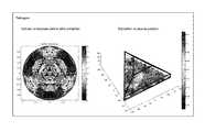
- FIGS. 3 and 4are illustrations of conventional and novel shaped chips according to some embodiments.
- topis a conventional cubic shape.
- the conventional cubic shapecan be inefficient as light could reflect many times (and therefore decay) before exiting from the device.
- Triangular shaped devicesshown at bottom left, provides better light extraction efficiency than the cubic shaped device. It is therefore to be appreciated that various embodiments provide three-dimensional shapes, tetragon shape on the bottom right, allow for better light extraction and less internal reflection. In a preferred embodiment, the present disclosure provides for a tetragon shaped device.
- FIG. 4illustrates various characteristics of the four shapes illustrated in FIG. 3 .
- the chip extraction value (Cex) valueis low at about 46.7% and the absorption value tends to be high at about 20%.
- the triangular shapeis associated with a higher extraction value at about 59.4% and absorption rate at about 12.7%, and thus the triangular shape is characterized by a better light extraction efficiency compared to the cubic shape.
- the pyramid shapeexhibits an even higher extraction rate (about 71.1%) and lower absorption rate (about 9.8%) compared to the triangular shape.
- the tetragon shapeexhibits the highest light extraction rate at about 79.8% and lowest absorption rate at about 6.5% among the four shapes.
- FIGS. 5 and 6are illustrations of a conventional square chip. As shown in FIG. 5 , the number of times that a light ray reflects within a cubic shaped device before exiting depends on the emission angle of the ray. As explained above, the light extraction characteristic is in accordance with Snell's law. FIG. 5 illustrates that when the angle is less than 0.4pi radians for both axes, light rays is extracted from the cubic device within a few number of reflections. However, at other angles, it typically takes many reflections, which can be over 20, before the light exits from the cubic shaped device. FIG. 6 illustrates that light extraction potential is only good at sidewalls and the top surface, where light rays can exit these surfaces at a substantially normal angle and no bouncing of light is needed.
- FIGS. 7 and 8are illustrations of a triangular chip according to an embodiment. As shown in FIG. 7 , when angle of light is small (e.g., less than 0.4) relative to the surface, it only takes very few reflections before light exits from the triangular shaped device. The bottom right drawing shows that much light is extracted from the triangular shaped device after one or more reflection. FIG. 8 shows that in various trajectories of light. As shown in the drawings to the right, light may exit from triangular shaped devices through various paths.
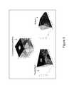
- FIGS. 9 and 10are illustrations of a pyramid shaped chip 904 .
- FIG. 9shows, at left, that most of the light can be extracted from various sides of the pyramid-shaped chip within a relatively few number of reflections (e.g., fewer than 10 reflections). More specifically, radiation emitted by the LED chip is able to exit from most surfaces of the pyramid and there are relatively few large areas where it requires more than 10 reflections before the radiation exits from the pyramid shaped chip.
- the graphillustrates a relationship between extraction and source position.
- FIG. 10shows trajectories of radiation for exiting the pyramid shaped chip 904 .
- the pyramid shapeallows radiation to exit from most sides (e.g., side 1002 1 , side 1002 2 ) of the chip, as the trajectory angles are typically below the threshold angle where the radiation is reflected. Also shown is an exemplary base 1004 , which base characteristics are further described herein.
- FIG. 11is an illustration of a pyramid shaped chip according to an embodiment.
- FIG. 9shows, at left, shows that most of the light can be extracted from regions and sides of the tetragon-shaped chip within a relatively few number of reflections.
- the tetragon-shaped chipdoes not contain a large area where radiation is “trapped” (i.e., internally reflected).
- the graphillustrates a relationship between extraction and source position.
- FIGS. 12 and 13are illustrations of effects of loss for shaped chips according to some embodiments. As shown in FIG. 12 , the tetragon shape is associated with less loss compared to the square shape, as demonstrated by the higher extraction index. FIG. 13 illustrates efficiencies respectively associated with conventional techniques and new techniques. In conventional techniques, the extraction efficiency is typically lower compared to embodiments. For example, in conventional techniques, a certain amount of loss is due to p-contact reflection losses.
- FIGS. 14 through 17are illustrations of light extraction and impact on chip shape geometry for tetragon shaped chips according to some embodiments.
- the geometry of the tetragon shaped chipaffects the extraction efficiency.
- the existence of a vertical sidewallis not detrimental.
- the vertical sidewallmay offer same benefit as triangular chip: horizontal rays are extracted after 2 reflections.
- the vertical sidewallmay impact the radiation diagram and die-to-die coupling. It is to be appreciated that embodiments offer flexibility in the optimal design, which could enable optimization in terms of manufacturability, chip resistivity or other device characteristics.
- FIG. 15illustrates effects of various aspects of the chip geometry on extraction efficiency. In general, increased chip height is associated with decreased p-metal loss, as shown, but increases substrate losses. The result is a predicted loss minima at a specific sidewall and total chip height.
- FIG. 16illustrates effects of lateral dimensions of a tetragon chip affecting extraction efficiency and losses. As shown in FIG. 16 , when the shape of the tetragon chip is kept constant (e.g., ratios h/x and k/x):
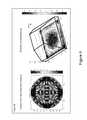
- FIG. 17is a diagram illustrating shaped device with a large radiation emitting surface according to an embodiment.
- the shape device shown in FIG. 17is formed from a substrate that has defect regions.
- the substrateconsists essentially of gallium nitride material, which is formed with a plurality of defect regions. As described above, defect regions are not suitable for being used for LED dies.
- the defect material regionsare positioned at the lateral sides of the shaped device.
- the top surface of the shaped devicehas a larger area than the bottom surface. It is to be appreciated that the large surface area on the top surface allows light emitted by the shaped device to be efficiently emitted out of the shaped device.
- both the n layer and p layerare located at the bottom of the shape device, which allows the electrical contacts to be located near the bottom of the device.
- the present disclosureprovides an arrangement of electrically conductive contacts that are positioned at bottom of light emitting diodes.
- FIG. 18is a diagram illustrating a shaped LED device where electrical contacts 1804 are positioned at the bottom according to some embodiments.
- n layer and p layerare both located at the bottom of an LED device.
- the LED devicecomprises gallium and nitrogen material.
- the n layer and the p layerare separated by an active region 1802.
- the n layeris electrically coupled to an n-contact
- the p layeris electrically coupled to a p contact.
- One or more mirrorsmay be employed to reflect a portion of generated photons.
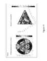
- FIG. 19A and FIG. 19Bdepict variations in chip shape geometry and corresponding impact on light extraction, according to some embodiments.
- the geometry diagram 1900 as shown in FIG. 19Adepicts a shaped LED device showing height k and vertical sidewall angle ⁇ of a tetragonal chip (e.g., having a triangular base). As the height k increases, the vertical sidewall angle ⁇ decreases, with the vertical sidewall angle ⁇ approaching zero for a large value of height k (e.g., while holding the independent geometric variables constant).
- FIG. 19Bdepicts a light extraction plot 1950 as plotted across of range of chip shape geometries.
- the amount of light extractionis given in the range gradient 1960 , with range gradient ranges from about 0.6 (60%) to about 0.85 (85%) as shown.
- the highest light extractioncan be obtained when vertical sidewall angle ⁇ is about 10° to about 25° and for a height k>200 um.
- the corresponding highest light extraction rangeis shown in area 1960 .
- the line 1910corresponds to the maximum value of k for a given vertical sidewall angle ⁇ .
- the base widthis shown as value b (which is 380 um in the case of FIG. 19B ). In exemplary embodiments, the value of b is in the range from about 50 um to about 5 mm.
- FIG. 20is a diagram illustrating a method of shaping a substrate structure containing gallium and nitrogen material.
- the methodcomprises steps for shaping a substrate structure containing gallium and nitrogen material that is to be used for manufacturing optical device, the method comprising: providing a gallium and nitrogen containing substrate member having a front region and a back region, the back region comprising a plurality of p-type contact regions (see operation 2010 ); subjecting a first street region between at least a first portion of a first die and a second die provided on the front region to at least a first saw process configured using a rotating blade structure having a tip region extending from a base region, the tip region being characterized by an angle of about 70 degrees and less to cause formation of a first trench region within the street region, the first trench region having a corresponding angle of about 65 degrees and less (see operation 2020 ); subjecting a second street region between at least a second portion of the first die and the second die provided on the front region to at least a second saw process configured using rotating blade structure having
- an optical devicecomprising a gallium and nitrogen containing substrate material having a selected active region area of less than 65,000 microns square formed overlying the substrate; and having an extraction efficiency characterized by a maximum emission region for the selected active region area. In some embodiments, the extraction efficiency ranges from about 70% to about 90%.
- the devicecan be shaped such that the gallium and nitrogen containing substrate material is configured in a non-orthogonal shape such as a tetragonal shape.
- the gallium and nitrogen containing substrate materialcan be configured as six pyramid shaped sides extending to respective six sides orthogonal to a base.
- the optical devicecan be configured as six pyramid shaped sides extending to respective six sides orthogonal to a base from a flat top.
- the shape of the basecan be characterized by a square shape, a hex shape, an annular shape, a rectangular shape, a circular shape, triangular, diamond.
- the gallium and nitrogen containing substrate materialcan be GaN, and can be configured as six pyramid shaped sides extending to respective six sides orthogonal to a base and a flat top.
- the shapecan be performed using any one or more techniques, for example, shaping the substrate structure can include dicing, laser ablating, scribing, polishing, chemical etching, dry etching, plasma etching, and/or telekinesis.
- the optical devicecan be configured of a gallium and nitrogen containing substrate structure, the structure comprising a base and at least six sides configured in a non-orthogonal spatial manner to the base; and having an active region configured in proximity to one or more mirror structures to cause a selective emission of electromagnetic radiation.
- the substrate structureis configured to provide a determined electromagnetic emission from the substrate structure, or wherein the optical device is one of a plurality of optical devices configured in an array pattern.
- a deviceis provided with a plurality of chips, the plurality of chips being arranged according to a predetermined spatial separation, the spatial separation being adjustable (e.g., at least 10 microns, about 10 microns, etc.).
- optical devicescan be isolated by separating small gallium and nitrogen containing chips from a substrate structure.
- One separation methodcan be performed by providing a patterned substrate comprising a backside region, the patterned substrate comprising a plurality of chips, each of the chips having a backside surface region; coupling the backside region of the substrate to a polymeric tape substrate to hold the patterned substrate on the tape substrate; subjecting the patterned substrate to a saw process to partially cut between at least two of the chips from the patterned substrate, the saw process being configured to cause a sheer force such that at least one of the chips detaches from the tape substrate if the blade penetrates through an entirety of a thickness of the substrate; removing the partially cut patterned substrate attached to the polymeric tape from the saw process; and breaking the patterned substrate to detach the chip.
- the saw processcomprises a suitable blade speed (e.g., 20,000 RPM to 70,000 RPM), and the saw process can comprise a feed speed of 0.5
Landscapes
- Led Devices (AREA)
Abstract
Description
- A model has predicted extraction efficiency and losses for a smooth chip;
- Tetragonal shape is desirable;
- Tetra chip geometry: keeping some vertical sidewall is useful. There is some design freedom both for height of sidewalls and lateral dimensions;
- Cavity effects boost extraction efficiency by a few %.
- For very small chips: n-pad loss dominates
- For very large chips: substrate loss dominates
- Optimal around X=350-500 um
- Note: in principle, the height value h, and the value k should be re-optimized for a given X.
Claims (28)
Priority Applications (1)
| Application Number | Priority Date | Filing Date | Title |
|---|---|---|---|
| US14/181,386US9076926B2 (en) | 2011-08-22 | 2014-02-14 | Gallium and nitrogen containing trilateral configuration for optical devices |
Applications Claiming Priority (3)
| Application Number | Priority Date | Filing Date | Title |
|---|---|---|---|
| US201161526136P | 2011-08-22 | 2011-08-22 | |
| US13/281,221US8686431B2 (en) | 2011-08-22 | 2011-10-25 | Gallium and nitrogen containing trilateral configuration for optical devices |
| US14/181,386US9076926B2 (en) | 2011-08-22 | 2014-02-14 | Gallium and nitrogen containing trilateral configuration for optical devices |
Related Parent Applications (1)
| Application Number | Title | Priority Date | Filing Date |
|---|---|---|---|
| US13/281,221ContinuationUS8686431B2 (en) | 2011-08-22 | 2011-10-25 | Gallium and nitrogen containing trilateral configuration for optical devices |
Publications (2)
| Publication Number | Publication Date |
|---|---|
| US20140346524A1 US20140346524A1 (en) | 2014-11-27 |
| US9076926B2true US9076926B2 (en) | 2015-07-07 |
Family
ID=46600048
Family Applications (2)
| Application Number | Title | Priority Date | Filing Date |
|---|---|---|---|
| US13/281,221Active2031-12-28US8686431B2 (en) | 2011-08-22 | 2011-10-25 | Gallium and nitrogen containing trilateral configuration for optical devices |
| US14/181,386ActiveUS9076926B2 (en) | 2011-08-22 | 2014-02-14 | Gallium and nitrogen containing trilateral configuration for optical devices |
Family Applications Before (1)
| Application Number | Title | Priority Date | Filing Date |
|---|---|---|---|
| US13/281,221Active2031-12-28US8686431B2 (en) | 2011-08-22 | 2011-10-25 | Gallium and nitrogen containing trilateral configuration for optical devices |
Country Status (1)
| Country | Link |
|---|---|
| US (2) | US8686431B2 (en) |
Families Citing this family (24)
| Publication number | Priority date | Publication date | Assignee | Title |
|---|---|---|---|---|
| US8247886B1 (en) | 2009-03-09 | 2012-08-21 | Soraa, Inc. | Polarization direction of optical devices using selected spatial configurations |
| US8299473B1 (en) | 2009-04-07 | 2012-10-30 | Soraa, Inc. | Polarized white light devices using non-polar or semipolar gallium containing materials and transparent phosphors |
| US8791499B1 (en) | 2009-05-27 | 2014-07-29 | Soraa, Inc. | GaN containing optical devices and method with ESD stability |
| US9000466B1 (en) | 2010-08-23 | 2015-04-07 | Soraa, Inc. | Methods and devices for light extraction from a group III-nitride volumetric LED using surface and sidewall roughening |
| US9293644B2 (en) | 2009-09-18 | 2016-03-22 | Soraa, Inc. | Power light emitting diode and method with uniform current density operation |
| CN102630349B (en) | 2009-09-18 | 2017-06-13 | 天空公司 | Power light emitting diode and method of operating with current density |
| US9583678B2 (en) | 2009-09-18 | 2017-02-28 | Soraa, Inc. | High-performance LED fabrication |
| US8933644B2 (en) | 2009-09-18 | 2015-01-13 | Soraa, Inc. | LED lamps with improved quality of light |
| US20110182056A1 (en)* | 2010-06-23 | 2011-07-28 | Soraa, Inc. | Quantum Dot Wavelength Conversion for Optical Devices Using Nonpolar or Semipolar Gallium Containing Materials |
| US8905588B2 (en) | 2010-02-03 | 2014-12-09 | Sorra, Inc. | System and method for providing color light sources in proximity to predetermined wavelength conversion structures |
| US8740413B1 (en) | 2010-02-03 | 2014-06-03 | Soraa, Inc. | System and method for providing color light sources in proximity to predetermined wavelength conversion structures |
| US10147850B1 (en) | 2010-02-03 | 2018-12-04 | Soraa, Inc. | System and method for providing color light sources in proximity to predetermined wavelength conversion structures |
| US9450143B2 (en) | 2010-06-18 | 2016-09-20 | Soraa, Inc. | Gallium and nitrogen containing triangular or diamond-shaped configuration for optical devices |
| US8786053B2 (en) | 2011-01-24 | 2014-07-22 | Soraa, Inc. | Gallium-nitride-on-handle substrate materials and devices and method of manufacture |
| US8686431B2 (en) | 2011-08-22 | 2014-04-01 | Soraa, Inc. | Gallium and nitrogen containing trilateral configuration for optical devices |
| US9646827B1 (en) | 2011-08-23 | 2017-05-09 | Soraa, Inc. | Method for smoothing surface of a substrate containing gallium and nitrogen |
| US8912025B2 (en) | 2011-11-23 | 2014-12-16 | Soraa, Inc. | Method for manufacture of bright GaN LEDs using a selective removal process |
| JP2015509669A (en) | 2012-03-06 | 2015-03-30 | ソラア インコーポレーテッドSoraa Inc. | Light emitting diode with low refractive index material layer to reduce guided light effect |
| US8971368B1 (en) | 2012-08-16 | 2015-03-03 | Soraa Laser Diode, Inc. | Laser devices having a gallium and nitrogen containing semipolar surface orientation |
| US9978904B2 (en) | 2012-10-16 | 2018-05-22 | Soraa, Inc. | Indium gallium nitride light emitting devices |
| US8802471B1 (en) | 2012-12-21 | 2014-08-12 | Soraa, Inc. | Contacts for an n-type gallium and nitrogen substrate for optical devices |
| US8994033B2 (en) | 2013-07-09 | 2015-03-31 | Soraa, Inc. | Contacts for an n-type gallium and nitrogen substrate for optical devices |
| US9419189B1 (en) | 2013-11-04 | 2016-08-16 | Soraa, Inc. | Small LED source with high brightness and high efficiency |
| JP2015207752A (en)* | 2014-04-08 | 2015-11-19 | パナソニックIpマネジメント株式会社 | Nitride semiconductor light emitting diode |
Citations (318)
| Publication number | Priority date | Publication date | Assignee | Title |
|---|---|---|---|---|
| US3647522A (en) | 1970-04-29 | 1972-03-07 | Motorola Inc | Method of reclaiming and coating phosphor |
| US4065688A (en) | 1977-03-28 | 1977-12-27 | Westinghouse Electric Corporation | High-pressure mercury-vapor discharge lamp having a light output with incandescent characteristics |
| US5366953A (en) | 1991-03-19 | 1994-11-22 | Conductus, Inc. | Method of forming grain boundary junctions in high temperature superconductor films |
| JPH06334215A (en) | 1993-05-18 | 1994-12-02 | Daido Steel Co Ltd | Surface emitting light emitting diode |
| JPH0936430A (en) | 1995-02-23 | 1997-02-07 | Nichia Chem Ind Ltd | Nitride semiconductor light emitting device |
| US5607899A (en) | 1994-02-25 | 1997-03-04 | Sumitomo Electric Industries, Ltd. | Method of forming single-crystalline thin film |
| JPH0982587A (en) | 1995-09-08 | 1997-03-28 | Hewlett Packard Co <Hp> | Preparation of nonsquare electronic chip |
| US5632812A (en) | 1993-03-10 | 1997-05-27 | Canon Kabushiki Kaisha | Diamond electronic device and process for producing the same |
| US5685885A (en) | 1990-09-24 | 1997-11-11 | Tessera, Inc. | Wafer-scale techniques for fabrication of semiconductor chip assemblies |
| US5764674A (en) | 1996-06-28 | 1998-06-09 | Honeywell Inc. | Current confinement for a vertical cavity surface emitting laser |
| US5813753A (en) | 1997-05-27 | 1998-09-29 | Philips Electronics North America Corporation | UV/blue led-phosphor device with efficient conversion of UV/blues light to visible light |
| US5926493A (en) | 1997-05-20 | 1999-07-20 | Sdl, Inc. | Optical semiconductor device with diffraction grating structure |
| EP0961328A2 (en) | 1998-05-28 | 1999-12-01 | Sumitomo Electric Industries, Ltd. | Gallium nitride-type semiconductor device |
| JPH11340507A (en)* | 1998-05-26 | 1999-12-10 | Matsushita Electron Corp | Semiconductor light-emitting element and its manufacture |
| US6069394A (en) | 1997-04-09 | 2000-05-30 | Matsushita Electronics Corporation | Semiconductor substrate, semiconductor device and method of manufacturing the same |
| US6072197A (en) | 1996-02-23 | 2000-06-06 | Fujitsu Limited | Semiconductor light emitting device with an active layer made of semiconductor having uniaxial anisotropy |
| JP2000294883A (en) | 1999-04-05 | 2000-10-20 | Nec Corp | Nitride compound semiconductor laser element |
| US6147953A (en) | 1998-03-25 | 2000-11-14 | Duncan Technologies, Inc. | Optical signal transmission apparatus |
| US6195381B1 (en) | 1998-04-27 | 2001-02-27 | Wisconsin Alumni Research Foundation | Narrow spectral width high-power distributed feedback semiconductor lasers |
| JP2001160627A (en) | 1999-11-30 | 2001-06-12 | Toyoda Gosei Co Ltd | Group III nitride compound semiconductor light emitting device |
| JP2001177146A (en) | 1999-12-21 | 2001-06-29 | Mitsubishi Cable Ind Ltd | Triangular semiconductor device and manufacturing method thereof |
| US20010009134A1 (en) | 1998-10-15 | 2001-07-26 | Lg Electronics Inc. | GaN system compound semiconductor and method for growing crystal thereof |
| US20010043042A1 (en) | 1998-08-18 | 2001-11-22 | Yoshinori Murazaki | Red light emitting long afterglow photoluminescence phosphor and afterglow lamp thereof |
| US20010055208A1 (en) | 2000-06-15 | 2001-12-27 | Koichi Kimura | Optical element, optical light source unit and optical display device equipped with the optical light source unit |
| US6335771B1 (en) | 1996-11-07 | 2002-01-01 | Sharp Kabushiki Kaisha | Liquid crystal display device, and methods of manufacturing and driving same |
| US20020027933A1 (en) | 2000-07-18 | 2002-03-07 | Rohm Co., Ltd. | Semiconductor light emitting device and semiconductor laser |
| US20020028564A1 (en) | 2000-07-10 | 2002-03-07 | Kensaku Motoki | Method of producing a single crystal gallium nitride substrate and single crystal gallium nitride substrate |
| US6379985B1 (en) | 2001-08-01 | 2002-04-30 | Xerox Corporation | Methods for cleaving facets in III-V nitrides grown on c-face sapphire substrates |
| US20020050488A1 (en) | 2000-03-01 | 2002-05-02 | Dmitri Nikitin | Method and apparatus for thermally processing quartz using a plurality of laser beams |
| US20020070416A1 (en) | 1999-12-09 | 2002-06-13 | The Regents Of The University Of California | Current isolating epitaxial buffer layers for high voltage photodiode array |
| JP2002185085A (en) | 2000-12-12 | 2002-06-28 | Sharp Corp | Nitride based semiconductor laser device and chip dividing method |
| US20020096994A1 (en) | 2000-07-18 | 2002-07-25 | Toshiaki Iwafuchi | Image display unit and method of producing image display unit |
| US20020127824A1 (en) | 1998-10-23 | 2002-09-12 | Shelton Bryan S. | Semiconductor wafer protection and cleaning for device separation using laser ablation |
| US20020190260A1 (en) | 1999-12-22 | 2002-12-19 | Yu-Chen Shen | Selective placement of quantum wells in flipchip light emitting diodes for improved light extraction |
| US6498355B1 (en) | 2001-10-09 | 2002-12-24 | Lumileds Lighting, U.S., Llc | High flux LED array |
| US6501154B2 (en) | 1997-06-03 | 2002-12-31 | Sony Corporation | Semiconductor substrate made of a nitride III-V compound semiconductor having a wurtzite-structured crystal structure |
| US20030000453A1 (en) | 2001-06-27 | 2003-01-02 | Yasuyuki Unno | Optical element and manufacturing method thereof |
| US20030001238A1 (en) | 2001-06-06 | 2003-01-02 | Matsushita Electric Industrial Co., Ltd. | GaN-based compound semiconductor EPI-wafer and semiconductor element using the same |
| US6509651B1 (en) | 1998-07-28 | 2003-01-21 | Sumitomo Electric Industries, Ltd. | Substrate-fluorescent LED |
| US20030020087A1 (en) | 2001-04-24 | 2003-01-30 | Osamu Goto | Nitride semiconductor, semiconductor device, and method of manufacturing the same |
| JP2003031844A (en) | 2001-07-11 | 2003-01-31 | Sony Corp | Method of manufacturing semiconductor light emitting device |
| US20030047076A1 (en) | 2001-09-10 | 2003-03-13 | Liu Jean H. | Dynamic filtration method and apparatus for separating nano powders |
| US6533874B1 (en) | 1996-12-03 | 2003-03-18 | Advanced Technology Materials, Inc. | GaN-based devices using thick (Ga, Al, In)N base layers |
| US20030080345A1 (en) | 2001-09-19 | 2003-05-01 | Sumitomo Electric Industries, Ltd. | Single crystal GaN substrate, method of growing same and method of producing same |
| US6586762B2 (en) | 2000-07-07 | 2003-07-01 | Nichia Corporation | Nitride semiconductor device with improved lifetime and high output power |
| US20030164507A1 (en) | 2000-11-03 | 2003-09-04 | Edmond John Adam | Group III nitride light emitting devices with progressively graded layers |
| US20030178617A1 (en) | 2002-03-20 | 2003-09-25 | International Business Machines Corporation | Self-aligned nanotube field effect transistor and method of fabricating same |
| US20030216011A1 (en) | 1992-11-20 | 2003-11-20 | Nichia Chemical Industries Ltd. | Light-emitting gallium nitride-based compound semiconductor device |
| US20040070004A1 (en) | 2000-11-16 | 2004-04-15 | Ivan Eliashevich | Led packages having improved light extraction |
| US20040080256A1 (en) | 1997-02-24 | 2004-04-29 | Hampden-Smith Mark J. | Oxygen-containing phosphor powders, methods for making phosphor powders and devices incorporating same |
| US6734461B1 (en) | 1999-09-07 | 2004-05-11 | Sixon Inc. | SiC wafer, SiC semiconductor device, and production method of SiC wafer |
| US20040104391A1 (en) | 2001-09-03 | 2004-06-03 | Toshihide Maeda | Semiconductor light emitting device, light emitting apparatus and production method for semiconductor light emitting device |
| US20040116033A1 (en) | 2003-01-27 | 2004-06-17 | 3M Innovative Properties Company | Methods of making phosphor based light sources having an interference reflector |
| US20040124435A1 (en) | 2002-12-27 | 2004-07-01 | General Electric Company | Homoepitaxial gallium-nitride-based electronic devices and method for producing same |
| US20040161222A1 (en) | 2003-02-18 | 2004-08-19 | Eiki Niida | Optical waveguide, area light source device and liquid crystal display device |
| US20040196877A1 (en) | 2003-04-01 | 2004-10-07 | Sharp Kabushiki Kaisha | Multi-wavelength laser device |
| US20040207998A1 (en) | 2003-03-10 | 2004-10-21 | Toyoda Gosei Co., Ltd. | Light emitting device |
| US6809781B2 (en) | 2002-09-24 | 2004-10-26 | General Electric Company | Phosphor blends and backlight sources for liquid crystal displays |
| US20040245543A1 (en) | 2003-06-04 | 2004-12-09 | Yoo Myung Cheol | Method of fabricating vertical structure compound semiconductor devices |
| US20040251471A1 (en) | 2001-10-26 | 2004-12-16 | Robert Dwilinski | Light emitting element structure using nitride bulk single crystal layer |
| US20050001227A1 (en) | 2001-07-24 | 2005-01-06 | Nichia Corporation | Semiconductor light-emitting device |
| US20050012446A1 (en) | 2003-05-28 | 2005-01-20 | Frank Jermann | Conversion led |
| US20050025205A1 (en) | 2003-04-24 | 2005-02-03 | Sharp Kabushiki Kaisha | Nitride semiconductor laser device |
| US6855959B2 (en) | 2000-03-24 | 2005-02-15 | Nec Corporation | Nitride based semiconductor photo-luminescent device |
| US6860628B2 (en) | 2002-07-17 | 2005-03-01 | Jonas J. Robertson | LED replacement for fluorescent lighting |
| US20050045894A1 (en) | 2000-12-15 | 2005-03-03 | Hiroyuki Okuyama | Semiconductor light emitting device and fabrication method thereof |
| US20050087753A1 (en) | 2003-10-24 | 2005-04-28 | D'evelyn Mark P. | Group III-nitride based resonant cavity light emitting devices fabricated on single crystal gallium nitride substrates |
| US20050095861A1 (en) | 2002-05-13 | 2005-05-05 | Sumitomo Electric Industries, Ltd. | GaN single-crystal substrate, nitride type semiconductor epitaxial substrate, nitride type semiconductor device, and methods of making the same |
| US20050109240A1 (en) | 2003-09-22 | 2005-05-26 | Fuji Photo Film Co., Ltd. | Organic pigment fine-particle, and method of producing the same |
| US20050121679A1 (en) | 1997-01-09 | 2005-06-09 | Nichia Chemical Industries, Ltd. | Nitride semiconductor device |
| US20050140270A1 (en) | 2003-12-02 | 2005-06-30 | Henson Gordon D. | Solid state light device |
| US20050139960A1 (en) | 2003-12-26 | 2005-06-30 | Hitachi Cable, Ltd. | III-V nitride semiconductor substrate and its production lot, and III-V nitride semiconductor device and its production method |
| US20050167680A1 (en) | 2004-02-02 | 2005-08-04 | Shih-Chang Shei | Light-emitting diode structure with electrostatic discharge protection |
| US20050199899A1 (en) | 2004-03-11 | 2005-09-15 | Ming-Der Lin | Package array and package unit of flip chip LED |
| US20050214992A1 (en) | 2002-12-16 | 2005-09-29 | The Regents Of The University Of California | Fabrication of nonpolar indium gallium nitride thin films, heterostructures and devices by metalorganic chemical vapor deposition |
| US20050224830A1 (en) | 2004-04-09 | 2005-10-13 | Blonder Greg E | Illumination devices comprising white light emitting diodes and diode arrays and method and apparatus for making them |
| US6956246B1 (en) | 2004-06-03 | 2005-10-18 | Lumileds Lighting U.S., Llc | Resonant cavity III-nitride light emitting devices fabricated by growth substrate removal |
| US20050232327A1 (en) | 2004-03-30 | 2005-10-20 | Yasuhiko Nomura | Integrated semiconductor laser diode module and manufacturing method of the same |
| US20050230701A1 (en) | 2004-04-16 | 2005-10-20 | Wen-Chieh Huang | High brightness gallium nitride-based light emitting diode with transparent conducting oxide spreading layer |
| US20050263791A1 (en) | 2003-01-17 | 2005-12-01 | Sanken Electric Co., Ltd. | Semiconductor device and a method of making the same |
| US20060038542A1 (en) | 2003-12-23 | 2006-02-23 | Tessera, Inc. | Solid state lighting device |
| US7009199B2 (en) | 2002-10-22 | 2006-03-07 | Cree, Inc. | Electronic devices having a header and antiparallel connected light emitting diodes for producing light from AC current |
| US7012279B2 (en) | 2003-10-21 | 2006-03-14 | Lumileds Lighting U.S., Llc | Photonic crystal light emitting device |
| US20060060131A1 (en) | 2003-12-29 | 2006-03-23 | Translucent, Inc. | Method of forming a rare-earth dielectric layer |
| US20060060872A1 (en) | 2004-09-22 | 2006-03-23 | Edmond John A | High output group III nitride light emitting diodes |
| US7019325B2 (en) | 2004-06-16 | 2006-03-28 | Exalos Ag | Broadband light emitting device |
| US20060079082A1 (en) | 2002-07-19 | 2006-04-13 | Cree, Inc. | Trench cut light emitting diodes and methods of fabricating same |
| US20060077795A1 (en) | 2004-09-01 | 2006-04-13 | Fujinon Corporation | Objective optical system for optical recording media and optical pickup device using it |
| US20060097278A1 (en) | 2002-06-20 | 2006-05-11 | Osamu Goto | Gan semiconductor device |
| WO2006062880A2 (en) | 2004-12-06 | 2006-06-15 | Sensor Electronic Technology, Inc. | Nitride-based light emitting heterostructure |
| JP2006173621A (en) | 2004-12-14 | 2006-06-29 | Palo Alto Research Center Inc | Semiconductor laser |
| US20060166390A1 (en) | 2005-01-13 | 2006-07-27 | Fabrice Letertre | Optoelectronic substrate and methods of making same |
| US20060163589A1 (en) | 2005-01-21 | 2006-07-27 | Zhaoyang Fan | Heterogeneous integrated high voltage DC/AC light emitter |
| US20060169993A1 (en) | 2005-02-03 | 2006-08-03 | Zhaoyang Fan | Micro-LED based high voltage AC/DC indicator lamp |
| US20060189098A1 (en) | 2005-02-23 | 2006-08-24 | Cree, Inc. | Substrate removal process for high light extraction LEDs |
| US20060186418A1 (en) | 2004-05-18 | 2006-08-24 | Edmond John A | External extraction light emitting diode based upon crystallographic faceted surfaces |
| US20060205199A1 (en) | 2005-03-10 | 2006-09-14 | The Regents Of The University Of California | Technique for the growth of planar semi-polar gallium nitride |
| US20060204865A1 (en) | 2005-03-08 | 2006-09-14 | Luminus Devices, Inc. | Patterned light-emitting devices |
| US20060214287A1 (en) | 2005-03-25 | 2006-09-28 | Mitsuhiko Ogihara | Semiconductor composite apparatus, print head, and image forming apparatus |
| US20060240585A1 (en) | 2004-10-28 | 2006-10-26 | Philips Lumileds Lighting Company, Llc | Package-Integrated Thin Film LED |
| US7128849B2 (en) | 2003-10-31 | 2006-10-31 | General Electric Company | Phosphors containing boron and metals of Group IIIA and IIIB |
| US20060255343A1 (en) | 2005-05-12 | 2006-11-16 | Oki Data Corporation | Semiconductor apparatus, print head, and image forming apparatus |
| US20060256482A1 (en) | 2005-05-10 | 2006-11-16 | Hitachi Global Storage Technologies Netherlands, B.V. | Method to fabricate side shields for a magnetic sensor |
| US20060273339A1 (en) | 2002-06-13 | 2006-12-07 | Philips Lumileds Lighting Company, Llc | Contacting Scheme for Large and Small Area Semiconductor Light Emitting Flip Chip Devices |
| US20060272572A1 (en) | 2005-06-06 | 2006-12-07 | Sumitomo Electric Industries, Ltd. | Nitride semiconductor substrate and method of producing same |
| US20060286695A1 (en) | 2004-03-30 | 2006-12-21 | Katsunori Yanashima | Method for producing semiconductor light emitting device, method for producing semiconductor device, method for producing device, method for growing nitride type iii-v group compound semiconductor layer, method for growing semiconductor layer, and method for growing layer |
| US20060288928A1 (en) | 2005-06-10 | 2006-12-28 | Chang-Beom Eom | Perovskite-based thin film structures on miscut semiconductor substrates |
| US20070045200A1 (en) | 2005-08-30 | 2007-03-01 | Moon Won J | Gathering method and apparatus of powder separated soluble component |
| US20070054476A1 (en) | 2005-09-05 | 2007-03-08 | Sumitomo Electric Industries. Ltd. | Method of producing a nitride semiconductor device and nitride semiconductor device |
| US20070062440A1 (en) | 2001-09-19 | 2007-03-22 | Sumitomo Electric Industries Ltd. | Gallium nitride crystal substrate and method of producing same |
| US20070072324A1 (en) | 2005-09-27 | 2007-03-29 | Lumileds Lighting U.S., Llc | Substrate for growing a III-V light emitting device |
| US7208096B2 (en) | 2002-06-26 | 2007-04-24 | Agency For Science, Technology And Research | Method of cleaving GaN/sapphire for forming laser mirror facets |
| US20070096239A1 (en) | 2005-10-31 | 2007-05-03 | General Electric Company | Semiconductor devices and methods of manufacture |
| US20070105351A1 (en) | 1997-10-30 | 2007-05-10 | Kensaku Motoki | GaN single crystal substrate and method of making the same |
| US20070114569A1 (en) | 2005-09-07 | 2007-05-24 | Cree, Inc. | Robust transistors with fluorine treatment |
| US20070121690A1 (en) | 2003-12-09 | 2007-05-31 | Tetsuo Fujii | Highly efficient gallium nitride based light emitting diodes via surface roughening |
| US20070131967A1 (en) | 2005-12-08 | 2007-06-14 | Hitachi Cable, Ltd. | Self-standing GaN single crystal substrate, method of making same, and method of making a nitride semiconductor device |
| US20070202624A1 (en) | 2006-02-24 | 2007-08-30 | Samsung Electro-Mechanics Co., Ltd. | Nitride-based semiconductor light-emitting device and method of manufacturing the same |
| US20070210074A1 (en) | 2006-02-24 | 2007-09-13 | Christoph Maurer | Surface heating element and method for producing a surface heating element |
| US20070217462A1 (en) | 2006-03-14 | 2007-09-20 | Sharp Kabushiki Kaisha | Nitride semiconductor laser device and method of producing the same |
| US20070228404A1 (en) | 2005-01-11 | 2007-10-04 | Tran Chuong A | Systems and methods for producing white-light light emitting diodes |
| US7285801B2 (en) | 2004-04-02 | 2007-10-23 | Lumination, Llc | LED with series-connected monolithically integrated mesas |
| US7303630B2 (en) | 2003-11-05 | 2007-12-04 | Sumitomo Electric Industries, Ltd. | Method of growing GaN crystal, method of producing single crystal GaN substrate, and single crystal GaN substrate |
| US20070290224A1 (en) | 2006-06-15 | 2007-12-20 | Sharp Kabushiki Kaisha | Method of manufacturing nitride semiconductor light-emitting element and nitride semiconductor light-emitting element |
| US20080001174A1 (en) | 2003-11-04 | 2008-01-03 | Hitachi Cable, Ltd. | III-V group nitride system semiconductor substrate |
| US20080023691A1 (en) | 2006-06-23 | 2008-01-31 | Jang Jun H | Light emitting diode having vertical topology and method of making the same |
| US20080030976A1 (en) | 2006-08-03 | 2008-02-07 | Yoshinori Murazaki | Light emitting apparatus |
| US20080054290A1 (en) | 2006-09-05 | 2008-03-06 | Epistar Corporation | Light emitting device and the manufacture method thereof |
| US7341880B2 (en) | 2003-09-17 | 2008-03-11 | Luminus Devices, Inc. | Light emitting device processes |
| US7348600B2 (en) | 2003-10-20 | 2008-03-25 | Nichia Corporation | Nitride semiconductor device, and its fabrication process |
| US20080073660A1 (en) | 2006-09-27 | 2008-03-27 | Mitsubishi Electric Corporation | Semiconductor light-emitting devices |
| US20080081015A1 (en) | 2006-10-02 | 2008-04-03 | Seiji Sarayama | Crystal producing apparatus, crystal producing method, substrate producing method, gallium nitride crystal, and gallium nitride substrate |
| US20080083741A1 (en) | 2006-09-14 | 2008-04-10 | General Electric Company | Heater, apparatus, and associated method |
| US20080083929A1 (en) | 2006-10-06 | 2008-04-10 | Iii-N Technology, Inc. | Ac/dc light emitting diodes with integrated protection mechanism |
| JP2008084973A (en) | 2006-09-26 | 2008-04-10 | Stanley Electric Co Ltd | Semiconductor light emitting device |
| US7358543B2 (en) | 2005-05-27 | 2008-04-15 | Avago Technologies Ecbu Ip (Singapore) Pte. Ltd. | Light emitting device having a layer of photonic crystals and a region of diffusing material and method for fabricating the device |
| US7358542B2 (en) | 2005-02-02 | 2008-04-15 | Lumination Llc | Red emitting phosphor materials for use in LED and LCD applications |
| US20080087919A1 (en) | 2006-10-08 | 2008-04-17 | Tysoe Steven A | Method for forming nitride crystals |
| US20080099777A1 (en) | 2005-10-19 | 2008-05-01 | Luminus Devices, Inc. | Light-emitting devices and related systems |
| US20080106212A1 (en) | 2006-11-08 | 2008-05-08 | Industrial Technology Research Institute | Alternating current light-emitting device and fabrication method thereof |
| US20080121906A1 (en) | 2004-08-20 | 2008-05-29 | Kenji Yakushiji | Method for Fabrication of Semiconductor Light-Emitting Device and the Device Fabricated by the Method |
| US20080121913A1 (en) | 2006-11-28 | 2008-05-29 | Mesophotonics Limited | Inverted-pyramidal photonic crystal light emitting device |
| US20080128752A1 (en) | 2006-11-13 | 2008-06-05 | Cree, Inc. | GaN based HEMTs with buried field plates |
| US20080142781A1 (en) | 2004-12-23 | 2008-06-19 | Lg Innotek Co., Ltd. | Nitride Semiconductor Light Emitting Device and Fabrication Method Thereof |
| US7390359B2 (en) | 2004-10-06 | 2008-06-24 | Sumitomo Electric Industries, Ltd. | Nitride semiconductor wafer |
| US20080151543A1 (en) | 2006-04-21 | 2008-06-26 | Xiaoping Wang | Ultra thin power led light with heat sink |
| US20080164578A1 (en) | 2006-12-28 | 2008-07-10 | Saint-Gobain Ceramics & Plastics, Inc. | Sapphire substrates and methods of making same |
| US20080164489A1 (en) | 2006-12-11 | 2008-07-10 | The Regents Of The University Of California | Metalorganic chemical vapor deposittion (MOCVD) growth of high performance non-polar III-nitride optical devices |
| US20080173884A1 (en) | 2007-01-22 | 2008-07-24 | Cree, Inc. | Wafer level phosphor coating method and devices fabricated utilizing method |
| US20080179610A1 (en) | 2006-10-23 | 2008-07-31 | Rohm Co., Ltd. | Semiconductor light emission device emitting polarized light and method for manufacturing the same |
| US20080179607A1 (en) | 2006-12-11 | 2008-07-31 | The Regents Of The University Of California | Non-polar and semi-polar light emitting devices |
| US20080191223A1 (en) | 2007-02-12 | 2008-08-14 | The Regents Of The University Of California | CLEAVED FACET (Ga,Al,In)N EDGE-EMITTING LASER DIODES GROWN ON SEMIPOLAR BULK GALLIUM NITRIDE SUBSTRATES |
| US20080191192A1 (en) | 2007-02-12 | 2008-08-14 | The Regents Of The University Of California | Al(x)Ga(1-x)N-CLADDING-FREE NONPOLAR III-NITRIDE BASED LASER DIODES AND LIGHT EMITTING DIODES |
| US20080194054A1 (en) | 2007-02-08 | 2008-08-14 | Hung-Yi Lin | Led array package structure having silicon substrate and method of making the same |
| US7419281B2 (en) | 2004-03-03 | 2008-09-02 | S.C. Johnson & Son, Inc. | LED light bulb with active ingredient emission |
| US20080210958A1 (en) | 2006-12-05 | 2008-09-04 | Rohm Co., Ltd. | Semiconductor white light emitting device and method for manufacturing the same |
| US20080211416A1 (en) | 2007-01-22 | 2008-09-04 | Led Lighting Fixtures, Inc. | Illumination devices using externally interconnected arrays of light emitting devices, and methods of fabricating same |
| US20080217745A1 (en) | 2006-12-19 | 2008-09-11 | Sumitomo Electric Industries, Ltd. | Nitride Semiconductor Wafer |
| US20080230765A1 (en) | 2007-03-19 | 2008-09-25 | Seoul Opto Device Co., Ltd. | Light emitting diode |
| US20080237569A1 (en) | 2007-03-26 | 2008-10-02 | Kabushiki Kaisha Toshiba | Semiconductor light emitting element, method for manufacturing the same, and light emitting device |
| US20080257256A1 (en) | 2001-07-06 | 2008-10-23 | Melnik Yuri V | BULK GaN AND AlGaN SINGLE CRYSTALS |
| US20080261381A1 (en) | 2007-04-18 | 2008-10-23 | Shin-Etsu Chemical Co., Ltd. | Method for manufacturing bonded substrate |
| US20080272463A1 (en) | 2004-09-27 | 2008-11-06 | Kenneth Scott Alexander Butcher | Method and Apparatus for Growing a Group (III) Metal Nitride Film and a Group (III) Metal Nitride Film |
| US20080282978A1 (en) | 2002-05-17 | 2008-11-20 | Kenneth Scott Alexander Butcher | Process For Manufacturing A Gallium Rich Gallium Nitride Film |
| US20080283851A1 (en) | 2007-05-17 | 2008-11-20 | Sumitomo Electric Industries, Ltd. | GaN Substrate, and Epitaxial Substrate and Semiconductor Light-Emitting Device Employing the Substrate |
| US20080284346A1 (en) | 2007-05-18 | 2008-11-20 | Samsung Electro-Mechanics Co., Ltd. | Light emitting diode array driving apparatus |
| US20080291961A1 (en) | 2005-12-16 | 2008-11-27 | Takeshi Kamikawa | Nitride semiconductor light emitting device and method of fabricating nitride semiconductor laser device |
| US20080298409A1 (en) | 2007-05-31 | 2008-12-04 | Sharp Kabushiki Kaisha | Nitride semiconductor laser chip and fabrication method thereof |
| US20080303033A1 (en) | 2007-06-05 | 2008-12-11 | Cree, Inc. | Formation of nitride-based optoelectronic and electronic device structures on lattice-matched substrates |
| JP2008311640A (en) | 2007-05-16 | 2008-12-25 | Rohm Co Ltd | Semiconductor laser diode |
| US7470555B2 (en) | 2000-06-08 | 2008-12-30 | Nichia Corporation | Semiconductor laser device, and method of manufacturing the same |
| JP2009021824A (en) | 2007-07-12 | 2009-01-29 | Mitsubishi Electric Corp | Directional coupler |
| US20090028204A1 (en) | 2007-07-24 | 2009-01-29 | Sanyo Electric Co., Ltd. | Semiconductor laser device |
| US20090032828A1 (en) | 2007-08-03 | 2009-02-05 | Philips Lumileds Lighting Company, Llc | III-Nitride Device Grown on Edge-Dislocation Template |
| US7489441B2 (en) | 2004-05-17 | 2009-02-10 | Carl Zeiss Smt Ag | Monocrystalline optical component with curved surface and multilayer coating |
| US7491984B2 (en) | 2000-03-31 | 2009-02-17 | Toyoda Gosei Co., Ltd. | Method for fabricating group III nitride compound semiconductors and group III nitride compound semiconductor devices |
| US20090058532A1 (en) | 2007-08-31 | 2009-03-05 | Fujitsu Limited | Nitride semiconductor device, doherty amplifier and drain voltage controlled amplifier |
| US20090065798A1 (en) | 2005-06-21 | 2009-03-12 | The Regents Of The University Of California | Packaging technique for the fabrication of polarized light emitting diodes |
| US20090072252A1 (en) | 2004-10-19 | 2009-03-19 | Hyo Kun Son | Nitride Semiconductor Light Emitting Device and Fabrication Method Therefor |
| US20090071394A1 (en) | 2001-10-09 | 2009-03-19 | Sumitomo Electronic Industries, Ltd. | AlxInyGa1-x-yN MIXTURE CRYSTAL SUBSTRATE, METHOD OF GROWING AlxInyGa1-x-yN MIXTURE CRYSTAL SUBSTRATE AND METHOD OF PRODUCING AlxInyGa1-x-yN MIXTURE CRYSTAL SUBSTRATE |
| US20090081857A1 (en) | 2007-09-14 | 2009-03-26 | Kyma Technologies, Inc. | Non-polar and semi-polar GaN substrates, devices, and methods for making them |
| US20090078955A1 (en) | 2007-09-26 | 2009-03-26 | Iii-N Technlogy, Inc | Micro-Emitter Array Based Full-Color Micro-Display |
| US20090078944A1 (en) | 2007-09-07 | 2009-03-26 | Rohm Co., Ltd. | Light emitting device and method of manufacturing the same |
| US20090086475A1 (en) | 2007-10-01 | 2009-04-02 | Intematix Corporation | Color tunable light emitting device |
| US20090095973A1 (en) | 2007-09-27 | 2009-04-16 | Rohm Co., Ltd. | Semiconductor light emitting device |
| US7535082B2 (en) | 2003-05-06 | 2009-05-19 | Sumitomo Electric Industries, Ltd. | Nitride semiconductor wafer and method of processing nitride semiconductor wafer |
| US20090140279A1 (en) | 2007-12-03 | 2009-06-04 | Goldeneye, Inc. | Substrate-free light emitting diode chip |
| US20090146170A1 (en) | 2007-11-30 | 2009-06-11 | The Regents Of The University Of California | High light extraction efficiency nitride based light emitting diode by surface roughening |
| US7550305B2 (en) | 2006-10-27 | 2009-06-23 | Canon Kabushiki Kaisha | Method of forming light-emitting element |
| US7566639B2 (en) | 2005-09-16 | 2009-07-28 | Rohm Co., Ltd. | Manufacturing method for nitride semiconductor device and nitride semiconductor light emitting device obtained with the same |
| US20090194796A1 (en) | 2005-03-04 | 2009-08-06 | Sumitomo Electric Industries, Ltd. | Vertical Gallium Nitride Semiconductor Device and Epitaxial Substrate |
| US20090206354A1 (en) | 2008-02-20 | 2009-08-20 | Hitachi Cable, Ltd. | Semiconductor light-emitting device |
| US20090227056A1 (en) | 2008-03-07 | 2009-09-10 | Sumitomo Electric Industries, Ltd. | Method of fabricating nitride semiconductor laser |
| US7598104B2 (en) | 2006-11-24 | 2009-10-06 | Agency For Science, Technology And Research | Method of forming a metal contact and passivation of a semiconductor feature |
| US20090252191A1 (en) | 2008-04-03 | 2009-10-08 | Rohm Co., Ltd. | Semiconductor laser device |
| US20090250686A1 (en) | 2008-04-04 | 2009-10-08 | The Regents Of The University Of California | METHOD FOR FABRICATION OF SEMIPOLAR (Al, In, Ga, B)N BASED LIGHT EMITTING DIODES |
| US20090267100A1 (en) | 2008-04-25 | 2009-10-29 | Sanyo Electric Co., Ltd. | Nitride-based semiconductor device and method of manufacturing the same |
| US20090267098A1 (en) | 2008-04-24 | 2009-10-29 | Sung Min Choi | Semiconductor light emitting device |
| US20090273005A1 (en) | 2006-07-24 | 2009-11-05 | Hung-Yi Lin | Opto-electronic package structure having silicon-substrate and method of forming the same |
| US7622742B2 (en) | 2003-07-03 | 2009-11-24 | Epivalley Co., Ltd. | III-nitride compound semiconductor light emitting device |
| US20090309127A1 (en) | 2008-06-13 | 2009-12-17 | Soraa, Inc. | Selective area epitaxy growth method and structure |
| US20090309110A1 (en) | 2008-06-16 | 2009-12-17 | Soraa, Inc. | Selective area epitaxy growth method and structure for multi-colored devices |
| US20090315480A1 (en) | 2008-06-18 | 2009-12-24 | Delta Electronics, Inc. | Brightness-adjustable led driving circuit |
| US20090315965A1 (en) | 2006-10-27 | 2009-12-24 | Canon Kabushiki Kaisha | Led array manufacturing method, led array and led printer |
| US20090321778A1 (en) | 2008-06-30 | 2009-12-31 | Advanced Optoelectronic Technology, Inc. | Flip-chip light emitting diode and method for fabricating the same |
| US20090321745A1 (en) | 2005-09-15 | 2009-12-31 | Panasonic Corporation | Semiconductor light-emitting device |
| US20100001300A1 (en) | 2008-06-25 | 2010-01-07 | Soraa, Inc. | COPACKING CONFIGURATIONS FOR NONPOLAR GaN AND/OR SEMIPOLAR GaN LEDs |
| US20100006876A1 (en) | 2008-07-10 | 2010-01-14 | Stanley Electric Co., Ltd. | Nitride semiconductor light emitting device with surface texture and its manufacture |
| US20100032691A1 (en) | 2008-08-05 | 2010-02-11 | Kim Yusik | Light emitting device, light emitting system having the same, and fabricating method of the light emitting device and the light emitting system |
| US20100032644A1 (en) | 2007-04-06 | 2010-02-11 | Sumitomo Electric Industries, Ltd. | Nitride Semiconductor Light-Emitting Device and Nitride Semiconductor Light-Emitting Device Fabrication Method |
| US20100055819A1 (en) | 2008-08-27 | 2010-03-04 | Yasuo Ohba | Method for manufacturing semiconductor light emitting device |
| US20100067241A1 (en) | 2008-09-16 | 2010-03-18 | Lapatovich Walter P | Optical Disk For Lighting Module |
| US20100096615A1 (en) | 2006-09-29 | 2010-04-22 | Rohm Co., Ltd. | Light-emitting device |
| US20100109030A1 (en) | 2008-11-06 | 2010-05-06 | Koninklijke Philips Electronics N.V. | Series connected flip chip leds with growth substrate removed |
| US20100108985A1 (en) | 2008-10-31 | 2010-05-06 | The Regents Of The University Of California | Optoelectronic device based on non-polar and semi-polar aluminum indium nitride and aluminum indium gallium nitride alloys |
| US20100117118A1 (en) | 2008-08-07 | 2010-05-13 | Dabiran Amir M | High electron mobility heterojunction device |
| US20100117101A1 (en) | 2007-03-13 | 2010-05-13 | Seoul Opto Device Co., Ltd. | Ac light emitting diode |
| US7718454B2 (en) | 2007-02-15 | 2010-05-18 | Mitsubishi Electric Corporation | Method for manufacturing a semiconductor laser |
| US7733571B1 (en) | 2007-07-24 | 2010-06-08 | Rockwell Collins, Inc. | Phosphor screen and displays systems |
| US20100140634A1 (en) | 2009-11-09 | 2010-06-10 | Cree Led Lighting Solutions, Inc. | Solid state emitter package including red and blue emitters |
| US20100148145A1 (en) | 2006-01-18 | 2010-06-17 | Akihiko Ishibashi | Nitride semiconductor light-emitting device |
| US20100149814A1 (en) | 2008-12-17 | 2010-06-17 | Lednovation, Inc. | Semiconductor Lighting Device With Wavelength Conversion on Back-Transferred Light Path |
| US20100155746A1 (en) | 2009-04-06 | 2010-06-24 | Cree, Inc. | High voltage low current surface-emitting led |
| US20100163887A1 (en) | 2008-12-31 | 2010-07-01 | Seoul Opto Device Co., Ltd. | Light emitting device having a plurality of non-polar light emitting cells and a method of fabricating the same |
| US20100187540A1 (en) | 2006-10-19 | 2010-07-29 | Sumitomo Electric Industries , Ltd. | Group iii nitride substrate, epitaxial layer-provided substrate, methods of manufacturing the same, and method of manufacturing semiconductor device |
| US20100200837A1 (en) | 2008-11-05 | 2010-08-12 | Goldeneye, Inc. | Dual sided processing and devices based on freestanding nitride and zinc oxide films |
| US20100240158A1 (en) | 2005-09-22 | 2010-09-23 | The Artak Ter-Hovhanissian Patent Trust | Led lighting with integrated heat sink and process for manufacturing same |
| US7816238B2 (en) | 2007-06-14 | 2010-10-19 | Sumitomo Electric Industries, Ltd. | GaN substrate, substrate with epitaxial layer, semiconductor device, and method of manufacturing GaN substrate |
| US20100276663A1 (en) | 2008-08-04 | 2010-11-04 | Sumitomo Electric Industries, Ltd. | Gan semiconductor optical element, method for manufacturing gan semiconductor optical element, epitaxial wafer and method for growing gan semiconductor film |
| US20100290208A1 (en) | 2009-05-13 | 2010-11-18 | Cree Led Lighting Solutions, Inc. | Solid state lighting devices having remote luminescent material-containing element, and lighting methods |
| US20100295054A1 (en) | 2007-06-08 | 2010-11-25 | Rohm Co., Ltd. | Semiconductor light-emitting element and method for fabricating the same |
| US20100295088A1 (en) | 2008-10-02 | 2010-11-25 | Soraa, Inc. | Textured-surface light emitting diode and method of manufacture |
| US20100302464A1 (en) | 2009-05-29 | 2010-12-02 | Soraa, Inc. | Laser Based Display Method and System |
| WO2010138923A1 (en) | 2009-05-29 | 2010-12-02 | Soraa, Inc. | Laser based display method and system |
| US20100316075A1 (en) | 2009-04-13 | 2010-12-16 | Kaai, Inc. | Optical Device Structure Using GaN Substrates for Laser Applications |
| US7858408B2 (en) | 2004-11-15 | 2010-12-28 | Koninklijke Philips Electronics N.V. | LED with phosphor tile and overmolded phosphor in lens |
| US20100327291A1 (en) | 2005-12-12 | 2010-12-30 | Kyma Technologies, Inc. | Single crystal group III nitride articles and method of producing same by HVPE method incorporating a polycrystalline layer for yield enhancement |
| US7862761B2 (en) | 2006-05-31 | 2011-01-04 | Canon Kabushiki Kaisha | Pattern forming method and pattern forming apparatus |
| US7871839B2 (en) | 2004-06-30 | 2011-01-18 | Seoul Opto Device Co., Ltd. | Light emitting element with a plurality of cells bonded, method of manufacturing the same, and light emitting device using the same |
| US20110017298A1 (en) | 2007-11-14 | 2011-01-27 | Stion Corporation | Multi-junction solar cell devices |
| US7884538B2 (en) | 2007-08-31 | 2011-02-08 | Kabushiki Kaisha Toshiba | Light-emitting device |
| US20110031508A1 (en) | 2009-05-01 | 2011-02-10 | Bridgelux, Inc. | Method and Apparatus for Manufacturing LED Devices using Laser Scribing |
| US7897988B2 (en) | 2006-12-18 | 2011-03-01 | Delta Electronics, Inc. | Electroluminescent device |
| US20110057167A1 (en) | 2008-09-11 | 2011-03-10 | Sumitomo Electric Industries, Ltd. | Nitride based semiconductor optical device, epitaxial wafer for nitride based semiconductor optical device, and method of fabricating semiconductor light-emitting device |
| US20110056429A1 (en) | 2009-08-21 | 2011-03-10 | Soraa, Inc. | Rapid Growth Method and Structures for Gallium and Nitrogen Containing Ultra-Thin Epitaxial Structures for Devices |
| US20110064100A1 (en) | 2009-09-17 | 2011-03-17 | Kaai, Inc. | Growth Structures and Method for Forming Laser Diodes on or Off Cut Gallium and Nitrogen Containing Substrates |
| US20110062415A1 (en) | 2009-08-21 | 2011-03-17 | The Regents Of The University Of California | Anisotropic strain control in semipolar nitride quantum wells by partially or fully relaxed aluminum indium gallium nitride layers with misfit dislocations |
| US20110064103A1 (en) | 2009-08-21 | 2011-03-17 | The Regents Of The University Of California | Semipolar nitride-based devices on partially or fully relaxed alloys with misfit dislocations at the heterointerface |
| US7923741B1 (en) | 2009-01-05 | 2011-04-12 | Lednovation, Inc. | Semiconductor lighting device with reflective remote wavelength conversion |
| US20110103418A1 (en) | 2009-11-03 | 2011-05-05 | The Regents Of The University Of California | Superluminescent diodes by crystallographic etching |
| US20110100291A1 (en) | 2009-01-29 | 2011-05-05 | Soraa, Inc. | Plant and method for large-scale ammonothermal manufacturing of gallium nitride boules |
| US20110108081A1 (en) | 2006-12-20 | 2011-05-12 | Jds Uniphase Corporation | Photovoltaic Power Converter |
| US20110121331A1 (en) | 2009-11-23 | 2011-05-26 | Koninklijke Philips Electronics N.V. | Wavelength converted semiconductor light emitting device |
| US7976630B2 (en) | 2008-09-11 | 2011-07-12 | Soraa, Inc. | Large-area seed for ammonothermal growth of bulk gallium nitride and method of manufacture |
| US20110177631A1 (en) | 2010-01-15 | 2011-07-21 | Koninklijke Philips Electronics N.V. | Method of forming a composite substrate and growing a iii-v light emitting device over the composite substrate |
| US20110175200A1 (en) | 2010-01-21 | 2011-07-21 | Hitachi Cable, Ltd. | Manufacturing method of conductive group iii nitride crystal, manufacturing method of conductive group iii nitride substrate and conductive group iii nitride substrate |
| US20110182056A1 (en) | 2010-06-23 | 2011-07-28 | Soraa, Inc. | Quantum Dot Wavelength Conversion for Optical Devices Using Nonpolar or Semipolar Gallium Containing Materials |
| US20110180781A1 (en) | 2008-06-05 | 2011-07-28 | Soraa, Inc | Highly Polarized White Light Source By Combining Blue LED on Semipolar or Nonpolar GaN with Yellow LED on Semipolar or Nonpolar GaN |
| US20110188530A1 (en) | 2007-12-21 | 2011-08-04 | Osram Opto Semiconductors Gmbh | Laser Light Source and Method for Producing a Laser Light Source |
| US20110186887A1 (en) | 2009-09-21 | 2011-08-04 | Soraa, Inc. | Reflection Mode Wavelength Conversion Material for Optical Devices Using Non-Polar or Semipolar Gallium Containing Materials |
| US20110186874A1 (en) | 2010-02-03 | 2011-08-04 | Soraa, Inc. | White Light Apparatus and Method |
| US20110216795A1 (en) | 2007-02-12 | 2011-09-08 | The Regents Of The University Of California | Semi-polar iii-nitride optoelectronic devices on m-plane substrates with miscuts less than +/-15 degrees in the c-direction |
| US20110220912A1 (en) | 2010-03-11 | 2011-09-15 | Soraa, Inc. | Semi-insulating Group III Metal Nitride and Method of Manufacture |
| US20110247556A1 (en) | 2010-03-31 | 2011-10-13 | Soraa, Inc. | Tapered Horizontal Growth Chamber |
| US20110256693A1 (en) | 2009-10-09 | 2011-10-20 | Soraa, Inc. | Method for Synthesis of High Quality Large Area Bulk Gallium Based Crystals |
| US8044412B2 (en) | 2006-01-20 | 2011-10-25 | Taiwan Semiconductor Manufacturing Company, Ltd | Package for a light emitting element |
| EP2381490A2 (en) | 2010-04-23 | 2011-10-26 | LG Innotek Co., Ltd | Light emitting device with electrode material having different Plasmon frequency differing from emitted light |
| US20110266552A1 (en) | 2010-04-29 | 2011-11-03 | Advanced Optoelectronic Technology, Inc. | Light emitting element and manufacturing method thereof |
| US20110281422A1 (en) | 2007-04-20 | 2011-11-17 | Lattice Power (Jiangxi) Corporation | Method for obtaining high-quality boundary for semiconductor devices fabricated on a partitioned substrate |
| US20110279054A1 (en) | 2009-09-18 | 2011-11-17 | Soraa, Inc. | Power Light Emitting Diode and Method with Current Density Operation |
| US20110317397A1 (en) | 2010-06-23 | 2011-12-29 | Soraa, Inc. | Quantum dot wavelength conversion for hermetically sealed optical devices |
| US20110315999A1 (en)* | 2010-06-18 | 2011-12-29 | Soraa, Inc. | Gallium and Nitrogen Containing Triangular or Diamond-shaped Configuration for Optical Devices |
| US20120000415A1 (en) | 2010-06-18 | 2012-01-05 | Soraa, Inc. | Large Area Nitride Crystal and Method for Making It |
| US20120007102A1 (en) | 2010-07-08 | 2012-01-12 | Soraa, Inc. | High Voltage Device and Method for Optical Devices |
| US20120043552A1 (en) | 2010-08-19 | 2012-02-23 | Soraa, Inc. | System and Method for Selected Pump LEDs with Multiple Phosphors |
| US8142566B2 (en) | 2004-08-06 | 2012-03-27 | Mitsubishi Chemical Corporation | Method for producing Ga-containing nitride semiconductor single crystal of BxAlyGazIn1-x-y-zNsPtAs1-s-t (0<=x<=1, 0<=y<1, 0<z<=1, 0<s<=1 and 0<=t<1) on a substrate |
| US20120073494A1 (en) | 2008-08-07 | 2012-03-29 | Soraa, Inc. | Process and Apparatus for Large-Scale Manufacturing of Bulk Monocrystalline Gallium-Containing Nitride |
| US8148801B2 (en) | 2008-08-25 | 2012-04-03 | Soraa, Inc. | Nitride crystal with removable surface layer and methods of manufacture |
| US8148180B2 (en) | 2011-07-15 | 2012-04-03 | Sorra, Inc. | Techniques of forming Ohmic contacts on GaN light emitting diodes |
| US8153475B1 (en) | 2009-08-18 | 2012-04-10 | Sorra, Inc. | Back-end processes for substrates re-use |
| US20120091465A1 (en) | 2010-10-13 | 2012-04-19 | Soraa, Inc. | Method of Making Bulk InGaN Substrates and Devices Thereon |
| US20120118223A1 (en) | 2008-06-05 | 2012-05-17 | Soraa, Inc. | High Pressure Apparatus and Method for Nitride Crystal Growth |
| US8188504B2 (en) | 2006-03-26 | 2012-05-29 | Lg Innotek Co., Ltd. | Light-emitting device and method for manufacturing the same including a light-emitting device and a protection device electrically connected by a connecting line |
| US20120135553A1 (en) | 2011-11-23 | 2012-05-31 | Soraa, Inc. | Method for Manufacture of Bright GaN LEDs Using a Selective Removal Process |
| US20120137966A1 (en) | 2009-09-29 | 2012-06-07 | Elmhurst Research, Inc. | High Pressure Apparatus with Stackable Rings |
| US8207548B2 (en) | 2003-08-28 | 2012-06-26 | Panasonic Corporation | Semiconductor light emitting device, light emitting module, lighting apparatus, display element and manufacturing method of semiconductor light emitting device |
| US8207554B2 (en) | 2009-09-11 | 2012-06-26 | Soraa, Inc. | System and method for LED packaging |
| USD662899S1 (en) | 2011-08-15 | 2012-07-03 | Soraa, Inc. | Heatsink |
| USD662900S1 (en) | 2011-08-15 | 2012-07-03 | Soraa, Inc. | Heatsink for LED |
| US20120187412A1 (en) | 2011-01-24 | 2012-07-26 | Soraa, Inc. | Gallium-Nitride-on-Handle Substrate Materials and Devices and Method of Manufacture |
| US20120199841A1 (en) | 2011-08-22 | 2012-08-09 | Soraa, Inc. | Gallium and Nitrogen Containing Trilateral Configuration for Optical Devices |
| US20120199952A1 (en) | 2012-01-09 | 2012-08-09 | Soraa, Inc. | Method for Growth of Indium-Containing Nitride Films |
| US8247887B1 (en) | 2009-05-29 | 2012-08-21 | Soraa, Inc. | Method and surface morphology of non-polar gallium nitride containing substrates |
| US8247886B1 (en) | 2009-03-09 | 2012-08-21 | Soraa, Inc. | Polarization direction of optical devices using selected spatial configurations |
| US8252662B1 (en) | 2009-03-28 | 2012-08-28 | Soraa, Inc. | Method and structure for manufacture of light emitting diode devices using bulk GaN |
| US8268643B2 (en) | 2008-09-08 | 2012-09-18 | Sumitomo Electric Industries, Ltd. | Substrate, epitaxial layer provided substrate, method for producing substrate, and method for producing epitaxial layer provided substrate |
| US8269245B1 (en) | 2009-10-30 | 2012-09-18 | Soraa, Inc. | Optical device with wavelength selective reflector |
| US8299473B1 (en) | 2009-04-07 | 2012-10-30 | Soraa, Inc. | Polarized white light devices using non-polar or semipolar gallium containing materials and transparent phosphors |
| US8304265B2 (en) | 2007-09-19 | 2012-11-06 | Sharp Kabushiki Kaisha | Color conversion filter and manufacturing method of the organic EL display |
| US8310143B2 (en) | 2006-08-23 | 2012-11-13 | Cree, Inc. | Lighting device and lighting method |
| US8313964B2 (en) | 2010-06-18 | 2012-11-20 | Soraa, Inc. | Singulation method and resulting device of thick gallium and nitrogen containing substrates |
| US8314429B1 (en) | 2009-09-14 | 2012-11-20 | Soraa, Inc. | Multi color active regions for white light emitting diode |
| US8324835B2 (en) | 2011-02-11 | 2012-12-04 | Soraa, Inc. | Modular LED lamp and manufacturing methods |
| US8350273B2 (en) | 2009-08-31 | 2013-01-08 | Infineon Technologies Ag | Semiconductor structure and a method of forming the same |
| US20130016750A1 (en) | 2009-05-29 | 2013-01-17 | Soraa, Inc. | Surface Morphology of Non-Polar Gallium Nitride Containing Substrates |
| US20130022758A1 (en) | 2012-01-27 | 2013-01-24 | Soraa, Inc. | Method and Resulting Device for Processing Phosphor Materials in Light Emitting Diode Applications |
| US20130022064A1 (en) | 2011-01-24 | 2013-01-24 | Soraa, Inc. | Laser Package Having Multiple Emitters Configured on a Substrate Member |
| US20130026483A1 (en) | 2010-06-18 | 2013-01-31 | Soraa, Inc. | Gallium and Nitrogen Containing Triangular or Diamond-Shaped Configuration for Optical Devices |
| US20130044782A1 (en) | 2009-04-13 | 2013-02-21 | Soraa, Inc. | Optical Device Structure Using GaN Substrates and Growth Structures for Laser Applications |
| US20130064261A1 (en) | 2008-08-04 | 2013-03-14 | Soraa, Inc. | Solid State Laser Device Using a Selected Crystal Orientation in Non-Polar or Semi-Polar GaN Containing Materials and Methods |
| US8431942B2 (en) | 2010-05-07 | 2013-04-30 | Koninklijke Philips Electronics N.V. | LED package with a rounded square lens |
| US8455894B1 (en) | 2008-10-17 | 2013-06-04 | Soraa, Inc. | Photonic-crystal light emitting diode and method of manufacture |
| US8477259B2 (en) | 2008-10-30 | 2013-07-02 | Hitachi Consumer Electronics Co., Ltd. | Liquid crystal display device |
| US20130234108A1 (en) | 2012-03-06 | 2013-09-12 | Soraa, Inc. | Light emitting diodes with low refractive index material layers to reduce light guiding effects |
| US8597967B1 (en) | 2010-11-17 | 2013-12-03 | Soraa, Inc. | Method and system for dicing substrates containing gallium and nitrogen material |
| US20140103356A1 (en) | 2012-10-16 | 2014-04-17 | Soraa, Inc. | Indium gallium nitride light emitting devices |
| US20140175492A1 (en) | 2012-12-21 | 2014-06-26 | Soraa, Inc. | Dense-luminescent-materials-coated violet leds |
| US8791499B1 (en) | 2009-05-27 | 2014-07-29 | Soraa, Inc. | GaN containing optical devices and method with ESD stability |
- 2011
- 2011-10-25USUS13/281,221patent/US8686431B2/enactiveActive
- 2014
- 2014-02-14USUS14/181,386patent/US9076926B2/enactiveActive
Patent Citations (348)
| Publication number | Priority date | Publication date | Assignee | Title |
|---|---|---|---|---|
| US3647522A (en) | 1970-04-29 | 1972-03-07 | Motorola Inc | Method of reclaiming and coating phosphor |
| US4065688A (en) | 1977-03-28 | 1977-12-27 | Westinghouse Electric Corporation | High-pressure mercury-vapor discharge lamp having a light output with incandescent characteristics |
| US5685885A (en) | 1990-09-24 | 1997-11-11 | Tessera, Inc. | Wafer-scale techniques for fabrication of semiconductor chip assemblies |
| US5366953A (en) | 1991-03-19 | 1994-11-22 | Conductus, Inc. | Method of forming grain boundary junctions in high temperature superconductor films |
| US20030216011A1 (en) | 1992-11-20 | 2003-11-20 | Nichia Chemical Industries Ltd. | Light-emitting gallium nitride-based compound semiconductor device |
| US5632812A (en) | 1993-03-10 | 1997-05-27 | Canon Kabushiki Kaisha | Diamond electronic device and process for producing the same |
| JPH06334215A (en) | 1993-05-18 | 1994-12-02 | Daido Steel Co Ltd | Surface emitting light emitting diode |
| US5607899A (en) | 1994-02-25 | 1997-03-04 | Sumitomo Electric Industries, Ltd. | Method of forming single-crystalline thin film |
| JPH0936430A (en) | 1995-02-23 | 1997-02-07 | Nichia Chem Ind Ltd | Nitride semiconductor light emitting device |
| JPH0982587A (en) | 1995-09-08 | 1997-03-28 | Hewlett Packard Co <Hp> | Preparation of nonsquare electronic chip |
| US6072197A (en) | 1996-02-23 | 2000-06-06 | Fujitsu Limited | Semiconductor light emitting device with an active layer made of semiconductor having uniaxial anisotropy |
| US5764674A (en) | 1996-06-28 | 1998-06-09 | Honeywell Inc. | Current confinement for a vertical cavity surface emitting laser |
| US6335771B1 (en) | 1996-11-07 | 2002-01-01 | Sharp Kabushiki Kaisha | Liquid crystal display device, and methods of manufacturing and driving same |
| US6533874B1 (en) | 1996-12-03 | 2003-03-18 | Advanced Technology Materials, Inc. | GaN-based devices using thick (Ga, Al, In)N base layers |
| US20050121679A1 (en) | 1997-01-09 | 2005-06-09 | Nichia Chemical Industries, Ltd. | Nitride semiconductor device |
| US20040080256A1 (en) | 1997-02-24 | 2004-04-29 | Hampden-Smith Mark J. | Oxygen-containing phosphor powders, methods for making phosphor powders and devices incorporating same |
| US6069394A (en) | 1997-04-09 | 2000-05-30 | Matsushita Electronics Corporation | Semiconductor substrate, semiconductor device and method of manufacturing the same |
| US5926493A (en) | 1997-05-20 | 1999-07-20 | Sdl, Inc. | Optical semiconductor device with diffraction grating structure |
| US5813753A (en) | 1997-05-27 | 1998-09-29 | Philips Electronics North America Corporation | UV/blue led-phosphor device with efficient conversion of UV/blues light to visible light |
| US6501154B2 (en) | 1997-06-03 | 2002-12-31 | Sony Corporation | Semiconductor substrate made of a nitride III-V compound semiconductor having a wurtzite-structured crystal structure |
| US20070105351A1 (en) | 1997-10-30 | 2007-05-10 | Kensaku Motoki | GaN single crystal substrate and method of making the same |
| US6147953A (en) | 1998-03-25 | 2000-11-14 | Duncan Technologies, Inc. | Optical signal transmission apparatus |
| US6195381B1 (en) | 1998-04-27 | 2001-02-27 | Wisconsin Alumni Research Foundation | Narrow spectral width high-power distributed feedback semiconductor lasers |
| JPH11340507A (en)* | 1998-05-26 | 1999-12-10 | Matsushita Electron Corp | Semiconductor light-emitting element and its manufacture |
| EP0961328A2 (en) | 1998-05-28 | 1999-12-01 | Sumitomo Electric Industries, Ltd. | Gallium nitride-type semiconductor device |
| JPH11340576A (en) | 1998-05-28 | 1999-12-10 | Sumitomo Electric Ind Ltd | Gallium nitride based semiconductor devices |
| US6509651B1 (en) | 1998-07-28 | 2003-01-21 | Sumitomo Electric Industries, Ltd. | Substrate-fluorescent LED |
| US20010043042A1 (en) | 1998-08-18 | 2001-11-22 | Yoshinori Murazaki | Red light emitting long afterglow photoluminescence phosphor and afterglow lamp thereof |
| US20010009134A1 (en) | 1998-10-15 | 2001-07-26 | Lg Electronics Inc. | GaN system compound semiconductor and method for growing crystal thereof |
| US20020127824A1 (en) | 1998-10-23 | 2002-09-12 | Shelton Bryan S. | Semiconductor wafer protection and cleaning for device separation using laser ablation |
| JP2000294883A (en) | 1999-04-05 | 2000-10-20 | Nec Corp | Nitride compound semiconductor laser element |
| US6734461B1 (en) | 1999-09-07 | 2004-05-11 | Sixon Inc. | SiC wafer, SiC semiconductor device, and production method of SiC wafer |
| JP2001160627A (en) | 1999-11-30 | 2001-06-12 | Toyoda Gosei Co Ltd | Group III nitride compound semiconductor light emitting device |
| US20020070416A1 (en) | 1999-12-09 | 2002-06-13 | The Regents Of The University Of California | Current isolating epitaxial buffer layers for high voltage photodiode array |
| US20020182768A1 (en) | 1999-12-09 | 2002-12-05 | Morse Jeffrey D. | Current isolating epitaxial buffer layers for high voltage photodiode array |
| JP2001177146A (en) | 1999-12-21 | 2001-06-29 | Mitsubishi Cable Ind Ltd | Triangular semiconductor device and manufacturing method thereof |
| US20020190260A1 (en) | 1999-12-22 | 2002-12-19 | Yu-Chen Shen | Selective placement of quantum wells in flipchip light emitting diodes for improved light extraction |
| US20020050488A1 (en) | 2000-03-01 | 2002-05-02 | Dmitri Nikitin | Method and apparatus for thermally processing quartz using a plurality of laser beams |
| US6855959B2 (en) | 2000-03-24 | 2005-02-15 | Nec Corporation | Nitride based semiconductor photo-luminescent device |
| US7491984B2 (en) | 2000-03-31 | 2009-02-17 | Toyoda Gosei Co., Ltd. | Method for fabricating group III nitride compound semiconductors and group III nitride compound semiconductor devices |
| US7470555B2 (en) | 2000-06-08 | 2008-12-30 | Nichia Corporation | Semiconductor laser device, and method of manufacturing the same |
| US20010055208A1 (en) | 2000-06-15 | 2001-12-27 | Koichi Kimura | Optical element, optical light source unit and optical display device equipped with the optical light source unit |
| US6586762B2 (en) | 2000-07-07 | 2003-07-01 | Nichia Corporation | Nitride semiconductor device with improved lifetime and high output power |
| US6468882B2 (en) | 2000-07-10 | 2002-10-22 | Sumitomo Electric Industries, Ltd. | Method of producing a single crystal gallium nitride substrate and single crystal gallium nitride substrate |
| US20020028564A1 (en) | 2000-07-10 | 2002-03-07 | Kensaku Motoki | Method of producing a single crystal gallium nitride substrate and single crystal gallium nitride substrate |
| US20020096994A1 (en) | 2000-07-18 | 2002-07-25 | Toshiaki Iwafuchi | Image display unit and method of producing image display unit |
| US20020027933A1 (en) | 2000-07-18 | 2002-03-07 | Rohm Co., Ltd. | Semiconductor light emitting device and semiconductor laser |
| US6680959B2 (en) | 2000-07-18 | 2004-01-20 | Rohm Co., Ltd. | Semiconductor light emitting device and semiconductor laser |
| US20030164507A1 (en) | 2000-11-03 | 2003-09-04 | Edmond John Adam | Group III nitride light emitting devices with progressively graded layers |
| US20040070004A1 (en) | 2000-11-16 | 2004-04-15 | Ivan Eliashevich | Led packages having improved light extraction |
| JP2002185085A (en) | 2000-12-12 | 2002-06-28 | Sharp Corp | Nitride based semiconductor laser device and chip dividing method |
| US20050045894A1 (en) | 2000-12-15 | 2005-03-03 | Hiroyuki Okuyama | Semiconductor light emitting device and fabrication method thereof |
| US20030020087A1 (en) | 2001-04-24 | 2003-01-30 | Osamu Goto | Nitride semiconductor, semiconductor device, and method of manufacturing the same |
| US20030001238A1 (en) | 2001-06-06 | 2003-01-02 | Matsushita Electric Industrial Co., Ltd. | GaN-based compound semiconductor EPI-wafer and semiconductor element using the same |
| US20030000453A1 (en) | 2001-06-27 | 2003-01-02 | Yasuyuki Unno | Optical element and manufacturing method thereof |
| US20080257256A1 (en) | 2001-07-06 | 2008-10-23 | Melnik Yuri V | BULK GaN AND AlGaN SINGLE CRYSTALS |
| JP2003031844A (en) | 2001-07-11 | 2003-01-31 | Sony Corp | Method of manufacturing semiconductor light emitting device |
| US20050001227A1 (en) | 2001-07-24 | 2005-01-06 | Nichia Corporation | Semiconductor light-emitting device |
| US6379985B1 (en) | 2001-08-01 | 2002-04-30 | Xerox Corporation | Methods for cleaving facets in III-V nitrides grown on c-face sapphire substrates |
| US20040104391A1 (en) | 2001-09-03 | 2004-06-03 | Toshihide Maeda | Semiconductor light emitting device, light emitting apparatus and production method for semiconductor light emitting device |
| US20030047076A1 (en) | 2001-09-10 | 2003-03-13 | Liu Jean H. | Dynamic filtration method and apparatus for separating nano powders |
| US20030080345A1 (en) | 2001-09-19 | 2003-05-01 | Sumitomo Electric Industries, Ltd. | Single crystal GaN substrate, method of growing same and method of producing same |
| US20040089919A1 (en) | 2001-09-19 | 2004-05-13 | Sumitomo Electric Industries, Ltd. | Single crystal GaN substrate, method of growing same and method of producing same |
| US20070062440A1 (en) | 2001-09-19 | 2007-03-22 | Sumitomo Electric Industries Ltd. | Gallium nitride crystal substrate and method of producing same |
| US6498355B1 (en) | 2001-10-09 | 2002-12-24 | Lumileds Lighting, U.S., Llc | High flux LED array |
| US20090071394A1 (en) | 2001-10-09 | 2009-03-19 | Sumitomo Electronic Industries, Ltd. | AlxInyGa1-x-yN MIXTURE CRYSTAL SUBSTRATE, METHOD OF GROWING AlxInyGa1-x-yN MIXTURE CRYSTAL SUBSTRATE AND METHOD OF PRODUCING AlxInyGa1-x-yN MIXTURE CRYSTAL SUBSTRATE |
| US20040251471A1 (en) | 2001-10-26 | 2004-12-16 | Robert Dwilinski | Light emitting element structure using nitride bulk single crystal layer |
| US20030178617A1 (en) | 2002-03-20 | 2003-09-25 | International Business Machines Corporation | Self-aligned nanotube field effect transistor and method of fabricating same |
| US20050095861A1 (en) | 2002-05-13 | 2005-05-05 | Sumitomo Electric Industries, Ltd. | GaN single-crystal substrate, nitride type semiconductor epitaxial substrate, nitride type semiconductor device, and methods of making the same |
| US20080282978A1 (en) | 2002-05-17 | 2008-11-20 | Kenneth Scott Alexander Butcher | Process For Manufacturing A Gallium Rich Gallium Nitride Film |
| US20060273339A1 (en) | 2002-06-13 | 2006-12-07 | Philips Lumileds Lighting Company, Llc | Contacting Scheme for Large and Small Area Semiconductor Light Emitting Flip Chip Devices |
| US20060097278A1 (en) | 2002-06-20 | 2006-05-11 | Osamu Goto | Gan semiconductor device |
| US7208096B2 (en) | 2002-06-26 | 2007-04-24 | Agency For Science, Technology And Research | Method of cleaving GaN/sapphire for forming laser mirror facets |
| US6860628B2 (en) | 2002-07-17 | 2005-03-01 | Jonas J. Robertson | LED replacement for fluorescent lighting |
| US20060079082A1 (en) | 2002-07-19 | 2006-04-13 | Cree, Inc. | Trench cut light emitting diodes and methods of fabricating same |
| US6809781B2 (en) | 2002-09-24 | 2004-10-26 | General Electric Company | Phosphor blends and backlight sources for liquid crystal displays |
| US7009199B2 (en) | 2002-10-22 | 2006-03-07 | Cree, Inc. | Electronic devices having a header and antiparallel connected light emitting diodes for producing light from AC current |
| US20050214992A1 (en) | 2002-12-16 | 2005-09-29 | The Regents Of The University Of California | Fabrication of nonpolar indium gallium nitride thin films, heterostructures and devices by metalorganic chemical vapor deposition |
| US20040124435A1 (en) | 2002-12-27 | 2004-07-01 | General Electric Company | Homoepitaxial gallium-nitride-based electronic devices and method for producing same |
| US20050263791A1 (en) | 2003-01-17 | 2005-12-01 | Sanken Electric Co., Ltd. | Semiconductor device and a method of making the same |
| US20040116033A1 (en) | 2003-01-27 | 2004-06-17 | 3M Innovative Properties Company | Methods of making phosphor based light sources having an interference reflector |
| US20040161222A1 (en) | 2003-02-18 | 2004-08-19 | Eiki Niida | Optical waveguide, area light source device and liquid crystal display device |
| US20040207998A1 (en) | 2003-03-10 | 2004-10-21 | Toyoda Gosei Co., Ltd. | Light emitting device |
| US20040196877A1 (en) | 2003-04-01 | 2004-10-07 | Sharp Kabushiki Kaisha | Multi-wavelength laser device |
| US20050025205A1 (en) | 2003-04-24 | 2005-02-03 | Sharp Kabushiki Kaisha | Nitride semiconductor laser device |
| US7786488B2 (en) | 2003-05-06 | 2010-08-31 | Sumitomo Electric Industries, Ltd. | Nitride semiconductor wafer and method of processing nitride semiconductor wafer |
| US7535082B2 (en) | 2003-05-06 | 2009-05-19 | Sumitomo Electric Industries, Ltd. | Nitride semiconductor wafer and method of processing nitride semiconductor wafer |
| US8008165B2 (en) | 2003-05-06 | 2011-08-30 | Sumitomo Electric Industries, Ltd. | Nitride semiconductor wafer and method of processing nitride semiconductor wafer |
| US20050012446A1 (en) | 2003-05-28 | 2005-01-20 | Frank Jermann | Conversion led |
| US20040245543A1 (en) | 2003-06-04 | 2004-12-09 | Yoo Myung Cheol | Method of fabricating vertical structure compound semiconductor devices |
| US7622742B2 (en) | 2003-07-03 | 2009-11-24 | Epivalley Co., Ltd. | III-nitride compound semiconductor light emitting device |
| US8207548B2 (en) | 2003-08-28 | 2012-06-26 | Panasonic Corporation | Semiconductor light emitting device, light emitting module, lighting apparatus, display element and manufacturing method of semiconductor light emitting device |
| US7341880B2 (en) | 2003-09-17 | 2008-03-11 | Luminus Devices, Inc. | Light emitting device processes |
| US20050109240A1 (en) | 2003-09-22 | 2005-05-26 | Fuji Photo Film Co., Ltd. | Organic pigment fine-particle, and method of producing the same |
| US7348600B2 (en) | 2003-10-20 | 2008-03-25 | Nichia Corporation | Nitride semiconductor device, and its fabrication process |
| US7012279B2 (en) | 2003-10-21 | 2006-03-14 | Lumileds Lighting U.S., Llc | Photonic crystal light emitting device |
| US20060118799A1 (en) | 2003-10-24 | 2006-06-08 | General Electric Company | Resonant cavity light emitting devices and associated method |
| US20050087753A1 (en) | 2003-10-24 | 2005-04-28 | D'evelyn Mark P. | Group III-nitride based resonant cavity light emitting devices fabricated on single crystal gallium nitride substrates |
| US7128849B2 (en) | 2003-10-31 | 2006-10-31 | General Electric Company | Phosphors containing boron and metals of Group IIIA and IIIB |
| US20080001174A1 (en) | 2003-11-04 | 2008-01-03 | Hitachi Cable, Ltd. | III-V group nitride system semiconductor substrate |
| US7303630B2 (en) | 2003-11-05 | 2007-12-04 | Sumitomo Electric Industries, Ltd. | Method of growing GaN crystal, method of producing single crystal GaN substrate, and single crystal GaN substrate |
| US20050140270A1 (en) | 2003-12-02 | 2005-06-30 | Henson Gordon D. | Solid state light device |
| US20070121690A1 (en) | 2003-12-09 | 2007-05-31 | Tetsuo Fujii | Highly efficient gallium nitride based light emitting diodes via surface roughening |
| US20060038542A1 (en) | 2003-12-23 | 2006-02-23 | Tessera, Inc. | Solid state lighting device |
| US20050139960A1 (en) | 2003-12-26 | 2005-06-30 | Hitachi Cable, Ltd. | III-V nitride semiconductor substrate and its production lot, and III-V nitride semiconductor device and its production method |
| US20060060131A1 (en) | 2003-12-29 | 2006-03-23 | Translucent, Inc. | Method of forming a rare-earth dielectric layer |
| US20050167680A1 (en) | 2004-02-02 | 2005-08-04 | Shih-Chang Shei | Light-emitting diode structure with electrostatic discharge protection |
| US7419281B2 (en) | 2004-03-03 | 2008-09-02 | S.C. Johnson & Son, Inc. | LED light bulb with active ingredient emission |
| US20050199899A1 (en) | 2004-03-11 | 2005-09-15 | Ming-Der Lin | Package array and package unit of flip chip LED |
| US20060286695A1 (en) | 2004-03-30 | 2006-12-21 | Katsunori Yanashima | Method for producing semiconductor light emitting device, method for producing semiconductor device, method for producing device, method for growing nitride type iii-v group compound semiconductor layer, method for growing semiconductor layer, and method for growing layer |
| US20050232327A1 (en) | 2004-03-30 | 2005-10-20 | Yasuhiko Nomura | Integrated semiconductor laser diode module and manufacturing method of the same |
| US7285801B2 (en) | 2004-04-02 | 2007-10-23 | Lumination, Llc | LED with series-connected monolithically integrated mesas |
| US20050224830A1 (en) | 2004-04-09 | 2005-10-13 | Blonder Greg E | Illumination devices comprising white light emitting diodes and diode arrays and method and apparatus for making them |
| US20050230701A1 (en) | 2004-04-16 | 2005-10-20 | Wen-Chieh Huang | High brightness gallium nitride-based light emitting diode with transparent conducting oxide spreading layer |
| US7489441B2 (en) | 2004-05-17 | 2009-02-10 | Carl Zeiss Smt Ag | Monocrystalline optical component with curved surface and multilayer coating |
| US20060186418A1 (en) | 2004-05-18 | 2006-08-24 | Edmond John A | External extraction light emitting diode based upon crystallographic faceted surfaces |
| US6956246B1 (en) | 2004-06-03 | 2005-10-18 | Lumileds Lighting U.S., Llc | Resonant cavity III-nitride light emitting devices fabricated by growth substrate removal |
| US7019325B2 (en) | 2004-06-16 | 2006-03-28 | Exalos Ag | Broadband light emitting device |
| US8198643B2 (en) | 2004-06-30 | 2012-06-12 | Seoul Opto Device Co., Ltd. | Light emitting element with a plurality of cells bonded, method of manufacturing the same, and light emitting device using the same |
| US7871839B2 (en) | 2004-06-30 | 2011-01-18 | Seoul Opto Device Co., Ltd. | Light emitting element with a plurality of cells bonded, method of manufacturing the same, and light emitting device using the same |
| US8142566B2 (en) | 2004-08-06 | 2012-03-27 | Mitsubishi Chemical Corporation | Method for producing Ga-containing nitride semiconductor single crystal of BxAlyGazIn1-x-y-zNsPtAs1-s-t (0<=x<=1, 0<=y<1, 0<z<=1, 0<s<=1 and 0<=t<1) on a substrate |
| US20080121906A1 (en) | 2004-08-20 | 2008-05-29 | Kenji Yakushiji | Method for Fabrication of Semiconductor Light-Emitting Device and the Device Fabricated by the Method |
| US20060077795A1 (en) | 2004-09-01 | 2006-04-13 | Fujinon Corporation | Objective optical system for optical recording media and optical pickup device using it |
| US20060060872A1 (en) | 2004-09-22 | 2006-03-23 | Edmond John A | High output group III nitride light emitting diodes |
| US20080272463A1 (en) | 2004-09-27 | 2008-11-06 | Kenneth Scott Alexander Butcher | Method and Apparatus for Growing a Group (III) Metal Nitride Film and a Group (III) Metal Nitride Film |
| US7390359B2 (en) | 2004-10-06 | 2008-06-24 | Sumitomo Electric Industries, Ltd. | Nitride semiconductor wafer |
| US20090072252A1 (en) | 2004-10-19 | 2009-03-19 | Hyo Kun Son | Nitride Semiconductor Light Emitting Device and Fabrication Method Therefor |
| US20060240585A1 (en) | 2004-10-28 | 2006-10-26 | Philips Lumileds Lighting Company, Llc | Package-Integrated Thin Film LED |
| US20110057205A1 (en) | 2004-11-15 | 2011-03-10 | Koninklijke Philips Electronics N.V. | Led with phosphor tile and overmolded phosphor in lens |
| US7858408B2 (en) | 2004-11-15 | 2010-12-28 | Koninklijke Philips Electronics N.V. | LED with phosphor tile and overmolded phosphor in lens |
| WO2006062880A2 (en) | 2004-12-06 | 2006-06-15 | Sensor Electronic Technology, Inc. | Nitride-based light emitting heterostructure |
| JP2006173621A (en) | 2004-12-14 | 2006-06-29 | Palo Alto Research Center Inc | Semiconductor laser |
| US20080142781A1 (en) | 2004-12-23 | 2008-06-19 | Lg Innotek Co., Ltd. | Nitride Semiconductor Light Emitting Device and Fabrication Method Thereof |
| US20070228404A1 (en) | 2005-01-11 | 2007-10-04 | Tran Chuong A | Systems and methods for producing white-light light emitting diodes |
| US20060166390A1 (en) | 2005-01-13 | 2006-07-27 | Fabrice Letertre | Optoelectronic substrate and methods of making same |
| US20060163589A1 (en) | 2005-01-21 | 2006-07-27 | Zhaoyang Fan | Heterogeneous integrated high voltage DC/AC light emitter |
| US7358542B2 (en) | 2005-02-02 | 2008-04-15 | Lumination Llc | Red emitting phosphor materials for use in LED and LCD applications |
| US20060169993A1 (en) | 2005-02-03 | 2006-08-03 | Zhaoyang Fan | Micro-LED based high voltage AC/DC indicator lamp |
| US20060189098A1 (en) | 2005-02-23 | 2006-08-24 | Cree, Inc. | Substrate removal process for high light extraction LEDs |
| US20090194796A1 (en) | 2005-03-04 | 2009-08-06 | Sumitomo Electric Industries, Ltd. | Vertical Gallium Nitride Semiconductor Device and Epitaxial Substrate |
| US20060204865A1 (en) | 2005-03-08 | 2006-09-14 | Luminus Devices, Inc. | Patterned light-emitting devices |
| US20060205199A1 (en) | 2005-03-10 | 2006-09-14 | The Regents Of The University Of California | Technique for the growth of planar semi-polar gallium nitride |
| US20060214287A1 (en) | 2005-03-25 | 2006-09-28 | Mitsuhiko Ogihara | Semiconductor composite apparatus, print head, and image forming apparatus |
| US20060256482A1 (en) | 2005-05-10 | 2006-11-16 | Hitachi Global Storage Technologies Netherlands, B.V. | Method to fabricate side shields for a magnetic sensor |
| US20060255343A1 (en) | 2005-05-12 | 2006-11-16 | Oki Data Corporation | Semiconductor apparatus, print head, and image forming apparatus |
| US7358543B2 (en) | 2005-05-27 | 2008-04-15 | Avago Technologies Ecbu Ip (Singapore) Pte. Ltd. | Light emitting device having a layer of photonic crystals and a region of diffusing material and method for fabricating the device |
| US20060272572A1 (en) | 2005-06-06 | 2006-12-07 | Sumitomo Electric Industries, Ltd. | Nitride semiconductor substrate and method of producing same |
| US20090155989A1 (en) | 2005-06-06 | 2009-06-18 | Sumitomo Electric Industries, Ltd. | Nitride semiconductor substrate and method of producing same |
| US20060288928A1 (en) | 2005-06-10 | 2006-12-28 | Chang-Beom Eom | Perovskite-based thin film structures on miscut semiconductor substrates |
| US20090065798A1 (en) | 2005-06-21 | 2009-03-12 | The Regents Of The University Of California | Packaging technique for the fabrication of polarized light emitting diodes |
| US7518159B2 (en) | 2005-06-21 | 2009-04-14 | The Regents Of The University Of California | Packaging technique for the fabrication of polarized light emitting diodes |
| US20070045200A1 (en) | 2005-08-30 | 2007-03-01 | Moon Won J | Gathering method and apparatus of powder separated soluble component |
| US20070054476A1 (en) | 2005-09-05 | 2007-03-08 | Sumitomo Electric Industries. Ltd. | Method of producing a nitride semiconductor device and nitride semiconductor device |
| US20070114569A1 (en) | 2005-09-07 | 2007-05-24 | Cree, Inc. | Robust transistors with fluorine treatment |
| US20090321745A1 (en) | 2005-09-15 | 2009-12-31 | Panasonic Corporation | Semiconductor light-emitting device |
| US7566639B2 (en) | 2005-09-16 | 2009-07-28 | Rohm Co., Ltd. | Manufacturing method for nitride semiconductor device and nitride semiconductor light emitting device obtained with the same |
| US20100240158A1 (en) | 2005-09-22 | 2010-09-23 | The Artak Ter-Hovhanissian Patent Trust | Led lighting with integrated heat sink and process for manufacturing same |
| US20070072324A1 (en) | 2005-09-27 | 2007-03-29 | Lumileds Lighting U.S., Llc | Substrate for growing a III-V light emitting device |
| US20080099777A1 (en) | 2005-10-19 | 2008-05-01 | Luminus Devices, Inc. | Light-emitting devices and related systems |
| US20070096239A1 (en) | 2005-10-31 | 2007-05-03 | General Electric Company | Semiconductor devices and methods of manufacture |
| US20070131967A1 (en) | 2005-12-08 | 2007-06-14 | Hitachi Cable, Ltd. | Self-standing GaN single crystal substrate, method of making same, and method of making a nitride semiconductor device |
| US20100327291A1 (en) | 2005-12-12 | 2010-12-30 | Kyma Technologies, Inc. | Single crystal group III nitride articles and method of producing same by HVPE method incorporating a polycrystalline layer for yield enhancement |
| US20080291961A1 (en) | 2005-12-16 | 2008-11-27 | Takeshi Kamikawa | Nitride semiconductor light emitting device and method of fabricating nitride semiconductor laser device |
| US20100148145A1 (en) | 2006-01-18 | 2010-06-17 | Akihiko Ishibashi | Nitride semiconductor light-emitting device |
| US8044412B2 (en) | 2006-01-20 | 2011-10-25 | Taiwan Semiconductor Manufacturing Company, Ltd | Package for a light emitting element |
| US20070202624A1 (en) | 2006-02-24 | 2007-08-30 | Samsung Electro-Mechanics Co., Ltd. | Nitride-based semiconductor light-emitting device and method of manufacturing the same |
| US20070210074A1 (en) | 2006-02-24 | 2007-09-13 | Christoph Maurer | Surface heating element and method for producing a surface heating element |
| US20070217462A1 (en) | 2006-03-14 | 2007-09-20 | Sharp Kabushiki Kaisha | Nitride semiconductor laser device and method of producing the same |
| US8188504B2 (en) | 2006-03-26 | 2012-05-29 | Lg Innotek Co., Ltd. | Light-emitting device and method for manufacturing the same including a light-emitting device and a protection device electrically connected by a connecting line |
| US20080151543A1 (en) | 2006-04-21 | 2008-06-26 | Xiaoping Wang | Ultra thin power led light with heat sink |
| US7862761B2 (en) | 2006-05-31 | 2011-01-04 | Canon Kabushiki Kaisha | Pattern forming method and pattern forming apparatus |
| US20070290224A1 (en) | 2006-06-15 | 2007-12-20 | Sharp Kabushiki Kaisha | Method of manufacturing nitride semiconductor light-emitting element and nitride semiconductor light-emitting element |
| US20080023691A1 (en) | 2006-06-23 | 2008-01-31 | Jang Jun H | Light emitting diode having vertical topology and method of making the same |
| US20090273005A1 (en) | 2006-07-24 | 2009-11-05 | Hung-Yi Lin | Opto-electronic package structure having silicon-substrate and method of forming the same |
| US20080030976A1 (en) | 2006-08-03 | 2008-02-07 | Yoshinori Murazaki | Light emitting apparatus |
| US8310143B2 (en) | 2006-08-23 | 2012-11-13 | Cree, Inc. | Lighting device and lighting method |
| US20080054290A1 (en) | 2006-09-05 | 2008-03-06 | Epistar Corporation | Light emitting device and the manufacture method thereof |
| US20080083741A1 (en) | 2006-09-14 | 2008-04-10 | General Electric Company | Heater, apparatus, and associated method |
| JP2008084973A (en) | 2006-09-26 | 2008-04-10 | Stanley Electric Co Ltd | Semiconductor light emitting device |
| US20080073660A1 (en) | 2006-09-27 | 2008-03-27 | Mitsubishi Electric Corporation | Semiconductor light-emitting devices |
| US20100096615A1 (en) | 2006-09-29 | 2010-04-22 | Rohm Co., Ltd. | Light-emitting device |
| US20080081015A1 (en) | 2006-10-02 | 2008-04-03 | Seiji Sarayama | Crystal producing apparatus, crystal producing method, substrate producing method, gallium nitride crystal, and gallium nitride substrate |
| US20080083929A1 (en) | 2006-10-06 | 2008-04-10 | Iii-N Technology, Inc. | Ac/dc light emitting diodes with integrated protection mechanism |
| US20080087919A1 (en) | 2006-10-08 | 2008-04-17 | Tysoe Steven A | Method for forming nitride crystals |
| US20100187540A1 (en) | 2006-10-19 | 2010-07-29 | Sumitomo Electric Industries , Ltd. | Group iii nitride substrate, epitaxial layer-provided substrate, methods of manufacturing the same, and method of manufacturing semiconductor device |
| US20080179610A1 (en) | 2006-10-23 | 2008-07-31 | Rohm Co., Ltd. | Semiconductor light emission device emitting polarized light and method for manufacturing the same |
| US20090315965A1 (en) | 2006-10-27 | 2009-12-24 | Canon Kabushiki Kaisha | Led array manufacturing method, led array and led printer |
| US7550305B2 (en) | 2006-10-27 | 2009-06-23 | Canon Kabushiki Kaisha | Method of forming light-emitting element |
| US20080106212A1 (en) | 2006-11-08 | 2008-05-08 | Industrial Technology Research Institute | Alternating current light-emitting device and fabrication method thereof |
| US20080128752A1 (en) | 2006-11-13 | 2008-06-05 | Cree, Inc. | GaN based HEMTs with buried field plates |
| US7598104B2 (en) | 2006-11-24 | 2009-10-06 | Agency For Science, Technology And Research | Method of forming a metal contact and passivation of a semiconductor feature |
| US20080121913A1 (en) | 2006-11-28 | 2008-05-29 | Mesophotonics Limited | Inverted-pyramidal photonic crystal light emitting device |
| US20080210958A1 (en) | 2006-12-05 | 2008-09-04 | Rohm Co., Ltd. | Semiconductor white light emitting device and method for manufacturing the same |
| US20080164489A1 (en) | 2006-12-11 | 2008-07-10 | The Regents Of The University Of California | Metalorganic chemical vapor deposittion (MOCVD) growth of high performance non-polar III-nitride optical devices |
| US20080179607A1 (en) | 2006-12-11 | 2008-07-31 | The Regents Of The University Of California | Non-polar and semi-polar light emitting devices |
| US7897988B2 (en) | 2006-12-18 | 2011-03-01 | Delta Electronics, Inc. | Electroluminescent device |
| US20080217745A1 (en) | 2006-12-19 | 2008-09-11 | Sumitomo Electric Industries, Ltd. | Nitride Semiconductor Wafer |
| US20110108081A1 (en) | 2006-12-20 | 2011-05-12 | Jds Uniphase Corporation | Photovoltaic Power Converter |
| US20080164578A1 (en) | 2006-12-28 | 2008-07-10 | Saint-Gobain Ceramics & Plastics, Inc. | Sapphire substrates and methods of making same |
| US20080211416A1 (en) | 2007-01-22 | 2008-09-04 | Led Lighting Fixtures, Inc. | Illumination devices using externally interconnected arrays of light emitting devices, and methods of fabricating same |
| US20080173884A1 (en) | 2007-01-22 | 2008-07-24 | Cree, Inc. | Wafer level phosphor coating method and devices fabricated utilizing method |
| US20080194054A1 (en) | 2007-02-08 | 2008-08-14 | Hung-Yi Lin | Led array package structure having silicon substrate and method of making the same |
| US20080191192A1 (en) | 2007-02-12 | 2008-08-14 | The Regents Of The University Of California | Al(x)Ga(1-x)N-CLADDING-FREE NONPOLAR III-NITRIDE BASED LASER DIODES AND LIGHT EMITTING DIODES |
| US20080191223A1 (en) | 2007-02-12 | 2008-08-14 | The Regents Of The University Of California | CLEAVED FACET (Ga,Al,In)N EDGE-EMITTING LASER DIODES GROWN ON SEMIPOLAR BULK GALLIUM NITRIDE SUBSTRATES |
| US20110216795A1 (en) | 2007-02-12 | 2011-09-08 | The Regents Of The University Of California | Semi-polar iii-nitride optoelectronic devices on m-plane substrates with miscuts less than +/-15 degrees in the c-direction |
| US7718454B2 (en) | 2007-02-15 | 2010-05-18 | Mitsubishi Electric Corporation | Method for manufacturing a semiconductor laser |
| US20100117101A1 (en) | 2007-03-13 | 2010-05-13 | Seoul Opto Device Co., Ltd. | Ac light emitting diode |
| US20080230765A1 (en) | 2007-03-19 | 2008-09-25 | Seoul Opto Device Co., Ltd. | Light emitting diode |
| US20080237569A1 (en) | 2007-03-26 | 2008-10-02 | Kabushiki Kaisha Toshiba | Semiconductor light emitting element, method for manufacturing the same, and light emitting device |
| US20100032644A1 (en) | 2007-04-06 | 2010-02-11 | Sumitomo Electric Industries, Ltd. | Nitride Semiconductor Light-Emitting Device and Nitride Semiconductor Light-Emitting Device Fabrication Method |
| US20080261381A1 (en) | 2007-04-18 | 2008-10-23 | Shin-Etsu Chemical Co., Ltd. | Method for manufacturing bonded substrate |
| US20110281422A1 (en) | 2007-04-20 | 2011-11-17 | Lattice Power (Jiangxi) Corporation | Method for obtaining high-quality boundary for semiconductor devices fabricated on a partitioned substrate |
| JP2008311640A (en) | 2007-05-16 | 2008-12-25 | Rohm Co Ltd | Semiconductor laser diode |
| US20080283851A1 (en) | 2007-05-17 | 2008-11-20 | Sumitomo Electric Industries, Ltd. | GaN Substrate, and Epitaxial Substrate and Semiconductor Light-Emitting Device Employing the Substrate |
| US20080284346A1 (en) | 2007-05-18 | 2008-11-20 | Samsung Electro-Mechanics Co., Ltd. | Light emitting diode array driving apparatus |
| US20080298409A1 (en) | 2007-05-31 | 2008-12-04 | Sharp Kabushiki Kaisha | Nitride semiconductor laser chip and fabrication method thereof |
| US20080303033A1 (en) | 2007-06-05 | 2008-12-11 | Cree, Inc. | Formation of nitride-based optoelectronic and electronic device structures on lattice-matched substrates |
| US20100295054A1 (en) | 2007-06-08 | 2010-11-25 | Rohm Co., Ltd. | Semiconductor light-emitting element and method for fabricating the same |
| US7816238B2 (en) | 2007-06-14 | 2010-10-19 | Sumitomo Electric Industries, Ltd. | GaN substrate, substrate with epitaxial layer, semiconductor device, and method of manufacturing GaN substrate |
| JP2009021824A (en) | 2007-07-12 | 2009-01-29 | Mitsubishi Electric Corp | Directional coupler |
| US20090028204A1 (en) | 2007-07-24 | 2009-01-29 | Sanyo Electric Co., Ltd. | Semiconductor laser device |
| US7733571B1 (en) | 2007-07-24 | 2010-06-08 | Rockwell Collins, Inc. | Phosphor screen and displays systems |
| US20090032828A1 (en) | 2007-08-03 | 2009-02-05 | Philips Lumileds Lighting Company, Llc | III-Nitride Device Grown on Edge-Dislocation Template |
| US7884538B2 (en) | 2007-08-31 | 2011-02-08 | Kabushiki Kaisha Toshiba | Light-emitting device |
| US20090058532A1 (en) | 2007-08-31 | 2009-03-05 | Fujitsu Limited | Nitride semiconductor device, doherty amplifier and drain voltage controlled amplifier |
| US20090078944A1 (en) | 2007-09-07 | 2009-03-26 | Rohm Co., Ltd. | Light emitting device and method of manufacturing the same |
| US20090081857A1 (en) | 2007-09-14 | 2009-03-26 | Kyma Technologies, Inc. | Non-polar and semi-polar GaN substrates, devices, and methods for making them |
| US8304265B2 (en) | 2007-09-19 | 2012-11-06 | Sharp Kabushiki Kaisha | Color conversion filter and manufacturing method of the organic EL display |
| US20090078955A1 (en) | 2007-09-26 | 2009-03-26 | Iii-N Technlogy, Inc | Micro-Emitter Array Based Full-Color Micro-Display |
| US20090095973A1 (en) | 2007-09-27 | 2009-04-16 | Rohm Co., Ltd. | Semiconductor light emitting device |
| US20090086475A1 (en) | 2007-10-01 | 2009-04-02 | Intematix Corporation | Color tunable light emitting device |
| US20110017298A1 (en) | 2007-11-14 | 2011-01-27 | Stion Corporation | Multi-junction solar cell devices |
| US20090146170A1 (en) | 2007-11-30 | 2009-06-11 | The Regents Of The University Of California | High light extraction efficiency nitride based light emitting diode by surface roughening |
| US20090140279A1 (en) | 2007-12-03 | 2009-06-04 | Goldeneye, Inc. | Substrate-free light emitting diode chip |
| US20110188530A1 (en) | 2007-12-21 | 2011-08-04 | Osram Opto Semiconductors Gmbh | Laser Light Source and Method for Producing a Laser Light Source |
| US20090206354A1 (en) | 2008-02-20 | 2009-08-20 | Hitachi Cable, Ltd. | Semiconductor light-emitting device |
| US20090227056A1 (en) | 2008-03-07 | 2009-09-10 | Sumitomo Electric Industries, Ltd. | Method of fabricating nitride semiconductor laser |
| US20090252191A1 (en) | 2008-04-03 | 2009-10-08 | Rohm Co., Ltd. | Semiconductor laser device |
| US20090250686A1 (en) | 2008-04-04 | 2009-10-08 | The Regents Of The University Of California | METHOD FOR FABRICATION OF SEMIPOLAR (Al, In, Ga, B)N BASED LIGHT EMITTING DIODES |
| US20090267098A1 (en) | 2008-04-24 | 2009-10-29 | Sung Min Choi | Semiconductor light emitting device |
| US20090267100A1 (en) | 2008-04-25 | 2009-10-29 | Sanyo Electric Co., Ltd. | Nitride-based semiconductor device and method of manufacturing the same |
| US20110180781A1 (en) | 2008-06-05 | 2011-07-28 | Soraa, Inc | Highly Polarized White Light Source By Combining Blue LED on Semipolar or Nonpolar GaN with Yellow LED on Semipolar or Nonpolar GaN |
| US20120118223A1 (en) | 2008-06-05 | 2012-05-17 | Soraa, Inc. | High Pressure Apparatus and Method for Nitride Crystal Growth |
| US20090309127A1 (en) | 2008-06-13 | 2009-12-17 | Soraa, Inc. | Selective area epitaxy growth method and structure |
| US20090309110A1 (en) | 2008-06-16 | 2009-12-17 | Soraa, Inc. | Selective area epitaxy growth method and structure for multi-colored devices |
| US20090315480A1 (en) | 2008-06-18 | 2009-12-24 | Delta Electronics, Inc. | Brightness-adjustable led driving circuit |
| US20100006873A1 (en) | 2008-06-25 | 2010-01-14 | Soraa, Inc. | HIGHLY POLARIZED WHITE LIGHT SOURCE BY COMBINING BLUE LED ON SEMIPOLAR OR NONPOLAR GaN WITH YELLOW LED ON SEMIPOLAR OR NONPOLAR GaN |
| US20100001300A1 (en) | 2008-06-25 | 2010-01-07 | Soraa, Inc. | COPACKING CONFIGURATIONS FOR NONPOLAR GaN AND/OR SEMIPOLAR GaN LEDs |
| US20090321778A1 (en) | 2008-06-30 | 2009-12-31 | Advanced Optoelectronic Technology, Inc. | Flip-chip light emitting diode and method for fabricating the same |
| US20100006876A1 (en) | 2008-07-10 | 2010-01-14 | Stanley Electric Co., Ltd. | Nitride semiconductor light emitting device with surface texture and its manufacture |
| US20100276663A1 (en) | 2008-08-04 | 2010-11-04 | Sumitomo Electric Industries, Ltd. | Gan semiconductor optical element, method for manufacturing gan semiconductor optical element, epitaxial wafer and method for growing gan semiconductor film |
| US20130064261A1 (en) | 2008-08-04 | 2013-03-14 | Soraa, Inc. | Solid State Laser Device Using a Selected Crystal Orientation in Non-Polar or Semi-Polar GaN Containing Materials and Methods |
| US20100032691A1 (en) | 2008-08-05 | 2010-02-11 | Kim Yusik | Light emitting device, light emitting system having the same, and fabricating method of the light emitting device and the light emitting system |
| US20120073494A1 (en) | 2008-08-07 | 2012-03-29 | Soraa, Inc. | Process and Apparatus for Large-Scale Manufacturing of Bulk Monocrystalline Gallium-Containing Nitride |
| US20100117118A1 (en) | 2008-08-07 | 2010-05-13 | Dabiran Amir M | High electron mobility heterojunction device |
| US8148801B2 (en) | 2008-08-25 | 2012-04-03 | Soraa, Inc. | Nitride crystal with removable surface layer and methods of manufacture |
| US20120178215A1 (en) | 2008-08-25 | 2012-07-12 | Soraa, Inc. | Nitride Crystal with Removable Surface Layer and Methods of Manufacture |
| US20100055819A1 (en) | 2008-08-27 | 2010-03-04 | Yasuo Ohba | Method for manufacturing semiconductor light emitting device |
| US8268643B2 (en) | 2008-09-08 | 2012-09-18 | Sumitomo Electric Industries, Ltd. | Substrate, epitaxial layer provided substrate, method for producing substrate, and method for producing epitaxial layer provided substrate |
| US20110262773A1 (en) | 2008-09-11 | 2011-10-27 | Soraa, Inc | Ammonothermal Method for Growth of Bulk Gallium Nitride |
| US20110057167A1 (en) | 2008-09-11 | 2011-03-10 | Sumitomo Electric Industries, Ltd. | Nitride based semiconductor optical device, epitaxial wafer for nitride based semiconductor optical device, and method of fabricating semiconductor light-emitting device |
| US7976630B2 (en) | 2008-09-11 | 2011-07-12 | Soraa, Inc. | Large-area seed for ammonothermal growth of bulk gallium nitride and method of manufacture |
| US20100067241A1 (en) | 2008-09-16 | 2010-03-18 | Lapatovich Walter P | Optical Disk For Lighting Module |
| US20100295088A1 (en) | 2008-10-02 | 2010-11-25 | Soraa, Inc. | Textured-surface light emitting diode and method of manufacture |
| US8455894B1 (en) | 2008-10-17 | 2013-06-04 | Soraa, Inc. | Photonic-crystal light emitting diode and method of manufacture |
| US8477259B2 (en) | 2008-10-30 | 2013-07-02 | Hitachi Consumer Electronics Co., Ltd. | Liquid crystal display device |
| US20100108985A1 (en) | 2008-10-31 | 2010-05-06 | The Regents Of The University Of California | Optoelectronic device based on non-polar and semi-polar aluminum indium nitride and aluminum indium gallium nitride alloys |
| US20100200837A1 (en) | 2008-11-05 | 2010-08-12 | Goldeneye, Inc. | Dual sided processing and devices based on freestanding nitride and zinc oxide films |
| US20100109030A1 (en) | 2008-11-06 | 2010-05-06 | Koninklijke Philips Electronics N.V. | Series connected flip chip leds with growth substrate removed |
| US20100149814A1 (en) | 2008-12-17 | 2010-06-17 | Lednovation, Inc. | Semiconductor Lighting Device With Wavelength Conversion on Back-Transferred Light Path |
| US20100163887A1 (en) | 2008-12-31 | 2010-07-01 | Seoul Opto Device Co., Ltd. | Light emitting device having a plurality of non-polar light emitting cells and a method of fabricating the same |
| US7923741B1 (en) | 2009-01-05 | 2011-04-12 | Lednovation, Inc. | Semiconductor lighting device with reflective remote wavelength conversion |
| US20110100291A1 (en) | 2009-01-29 | 2011-05-05 | Soraa, Inc. | Plant and method for large-scale ammonothermal manufacturing of gallium nitride boules |
| US20120288974A1 (en) | 2009-03-09 | 2012-11-15 | Kaai, Inc. | Polarization Direction of Optical Devices Using Selected Spatial Configurations |
| US8247886B1 (en) | 2009-03-09 | 2012-08-21 | Soraa, Inc. | Polarization direction of optical devices using selected spatial configurations |
| US8252662B1 (en) | 2009-03-28 | 2012-08-28 | Soraa, Inc. | Method and structure for manufacture of light emitting diode devices using bulk GaN |
| US20100155746A1 (en) | 2009-04-06 | 2010-06-24 | Cree, Inc. | High voltage low current surface-emitting led |
| US8299473B1 (en) | 2009-04-07 | 2012-10-30 | Soraa, Inc. | Polarized white light devices using non-polar or semipolar gallium containing materials and transparent phosphors |
| US20100316075A1 (en) | 2009-04-13 | 2010-12-16 | Kaai, Inc. | Optical Device Structure Using GaN Substrates for Laser Applications |
| US20130044782A1 (en) | 2009-04-13 | 2013-02-21 | Soraa, Inc. | Optical Device Structure Using GaN Substrates and Growth Structures for Laser Applications |
| US20110031508A1 (en) | 2009-05-01 | 2011-02-10 | Bridgelux, Inc. | Method and Apparatus for Manufacturing LED Devices using Laser Scribing |
| US20100290208A1 (en) | 2009-05-13 | 2010-11-18 | Cree Led Lighting Solutions, Inc. | Solid state lighting devices having remote luminescent material-containing element, and lighting methods |
| US8791499B1 (en) | 2009-05-27 | 2014-07-29 | Soraa, Inc. | GaN containing optical devices and method with ESD stability |
| US8749030B2 (en) | 2009-05-29 | 2014-06-10 | Soraa, Inc. | Surface morphology of non-polar gallium nitride containing substrates |
| US20100302464A1 (en) | 2009-05-29 | 2010-12-02 | Soraa, Inc. | Laser Based Display Method and System |
| US20130016750A1 (en) | 2009-05-29 | 2013-01-17 | Soraa, Inc. | Surface Morphology of Non-Polar Gallium Nitride Containing Substrates |
| US8524578B1 (en) | 2009-05-29 | 2013-09-03 | Soraa, Inc. | Method and surface morphology of non-polar gallium nitride containing substrates |
| US8247887B1 (en) | 2009-05-29 | 2012-08-21 | Soraa, Inc. | Method and surface morphology of non-polar gallium nitride containing substrates |
| US8575728B1 (en) | 2009-05-29 | 2013-11-05 | Soraa, Inc. | Method and surface morphology of non-polar gallium nitride containing substrates |
| WO2010138923A1 (en) | 2009-05-29 | 2010-12-02 | Soraa, Inc. | Laser based display method and system |
| US8153475B1 (en) | 2009-08-18 | 2012-04-10 | Sorra, Inc. | Back-end processes for substrates re-use |
| US20110062415A1 (en) | 2009-08-21 | 2011-03-17 | The Regents Of The University Of California | Anisotropic strain control in semipolar nitride quantum wells by partially or fully relaxed aluminum indium gallium nitride layers with misfit dislocations |
| US20110064103A1 (en) | 2009-08-21 | 2011-03-17 | The Regents Of The University Of California | Semipolar nitride-based devices on partially or fully relaxed alloys with misfit dislocations at the heterointerface |
| US20110056429A1 (en) | 2009-08-21 | 2011-03-10 | Soraa, Inc. | Rapid Growth Method and Structures for Gallium and Nitrogen Containing Ultra-Thin Epitaxial Structures for Devices |
| US8350273B2 (en) | 2009-08-31 | 2013-01-08 | Infineon Technologies Ag | Semiconductor structure and a method of forming the same |
| US8207554B2 (en) | 2009-09-11 | 2012-06-26 | Soraa, Inc. | System and method for LED packaging |
| US20120235201A1 (en) | 2009-09-11 | 2012-09-20 | Soraa, Inc. | System and method for led packaging |
| US8314429B1 (en) | 2009-09-14 | 2012-11-20 | Soraa, Inc. | Multi color active regions for white light emitting diode |
| US8355418B2 (en) | 2009-09-17 | 2013-01-15 | Soraa, Inc. | Growth structures and method for forming laser diodes on {20-21} or off cut gallium and nitrogen containing substrates |
| US20110064100A1 (en) | 2009-09-17 | 2011-03-17 | Kaai, Inc. | Growth Structures and Method for Forming Laser Diodes on or Off Cut Gallium and Nitrogen Containing Substrates |
| US20110064102A1 (en) | 2009-09-17 | 2011-03-17 | Kaai, Inc. | Growth Structures and Method for Forming Laser Diodes on or Off Cut Gallium and Nitrogen Containing Substrates |
| US8351478B2 (en) | 2009-09-17 | 2013-01-08 | Soraa, Inc. | Growth structures and method for forming laser diodes on {30-31} or off cut gallium and nitrogen containing substrates |
| US20110064101A1 (en) | 2009-09-17 | 2011-03-17 | Kaai, Inc. | Low Voltage Laser Diodes on Gallium and Nitrogen Containing Substrates |
| US20110279054A1 (en) | 2009-09-18 | 2011-11-17 | Soraa, Inc. | Power Light Emitting Diode and Method with Current Density Operation |
| US8502465B2 (en) | 2009-09-18 | 2013-08-06 | Soraa, Inc. | Power light emitting diode and method with current density operation |
| US20110186887A1 (en) | 2009-09-21 | 2011-08-04 | Soraa, Inc. | Reflection Mode Wavelength Conversion Material for Optical Devices Using Non-Polar or Semipolar Gallium Containing Materials |
| US20120137966A1 (en) | 2009-09-29 | 2012-06-07 | Elmhurst Research, Inc. | High Pressure Apparatus with Stackable Rings |
| US20110256693A1 (en) | 2009-10-09 | 2011-10-20 | Soraa, Inc. | Method for Synthesis of High Quality Large Area Bulk Gallium Based Crystals |
| US8269245B1 (en) | 2009-10-30 | 2012-09-18 | Soraa, Inc. | Optical device with wavelength selective reflector |
| US20110103418A1 (en) | 2009-11-03 | 2011-05-05 | The Regents Of The University Of California | Superluminescent diodes by crystallographic etching |
| US20100140634A1 (en) | 2009-11-09 | 2010-06-10 | Cree Led Lighting Solutions, Inc. | Solid state emitter package including red and blue emitters |
| US20110121331A1 (en) | 2009-11-23 | 2011-05-26 | Koninklijke Philips Electronics N.V. | Wavelength converted semiconductor light emitting device |
| US20110177631A1 (en) | 2010-01-15 | 2011-07-21 | Koninklijke Philips Electronics N.V. | Method of forming a composite substrate and growing a iii-v light emitting device over the composite substrate |
| US20110175200A1 (en) | 2010-01-21 | 2011-07-21 | Hitachi Cable, Ltd. | Manufacturing method of conductive group iii nitride crystal, manufacturing method of conductive group iii nitride substrate and conductive group iii nitride substrate |
| US20110186874A1 (en) | 2010-02-03 | 2011-08-04 | Soraa, Inc. | White Light Apparatus and Method |
| US20110220912A1 (en) | 2010-03-11 | 2011-09-15 | Soraa, Inc. | Semi-insulating Group III Metal Nitride and Method of Manufacture |
| US20110247556A1 (en) | 2010-03-31 | 2011-10-13 | Soraa, Inc. | Tapered Horizontal Growth Chamber |
| EP2381490A2 (en) | 2010-04-23 | 2011-10-26 | LG Innotek Co., Ltd | Light emitting device with electrode material having different Plasmon frequency differing from emitted light |
| US20110266552A1 (en) | 2010-04-29 | 2011-11-03 | Advanced Optoelectronic Technology, Inc. | Light emitting element and manufacturing method thereof |
| US8431942B2 (en) | 2010-05-07 | 2013-04-30 | Koninklijke Philips Electronics N.V. | LED package with a rounded square lens |
| US8313964B2 (en) | 2010-06-18 | 2012-11-20 | Soraa, Inc. | Singulation method and resulting device of thick gallium and nitrogen containing substrates |
| US20130026483A1 (en) | 2010-06-18 | 2013-01-31 | Soraa, Inc. | Gallium and Nitrogen Containing Triangular or Diamond-Shaped Configuration for Optical Devices |
| US20110315999A1 (en)* | 2010-06-18 | 2011-12-29 | Soraa, Inc. | Gallium and Nitrogen Containing Triangular or Diamond-shaped Configuration for Optical Devices |
| US20120000415A1 (en) | 2010-06-18 | 2012-01-05 | Soraa, Inc. | Large Area Nitride Crystal and Method for Making It |
| US8293551B2 (en) | 2010-06-18 | 2012-10-23 | Soraa, Inc. | Gallium and nitrogen containing triangular or diamond-shaped configuration for optical devices |
| US20110182056A1 (en) | 2010-06-23 | 2011-07-28 | Soraa, Inc. | Quantum Dot Wavelength Conversion for Optical Devices Using Nonpolar or Semipolar Gallium Containing Materials |
| US20110317397A1 (en) | 2010-06-23 | 2011-12-29 | Soraa, Inc. | Quantum dot wavelength conversion for hermetically sealed optical devices |
| US20120007102A1 (en) | 2010-07-08 | 2012-01-12 | Soraa, Inc. | High Voltage Device and Method for Optical Devices |
| US20120043552A1 (en) | 2010-08-19 | 2012-02-23 | Soraa, Inc. | System and Method for Selected Pump LEDs with Multiple Phosphors |
| US20120091465A1 (en) | 2010-10-13 | 2012-04-19 | Soraa, Inc. | Method of Making Bulk InGaN Substrates and Devices Thereon |
| US8597967B1 (en) | 2010-11-17 | 2013-12-03 | Soraa, Inc. | Method and system for dicing substrates containing gallium and nitrogen material |
| US20120187412A1 (en) | 2011-01-24 | 2012-07-26 | Soraa, Inc. | Gallium-Nitride-on-Handle Substrate Materials and Devices and Method of Manufacture |
| US20140346546A1 (en) | 2011-01-24 | 2014-11-27 | Soraa, Inc. | Gallium-nitride-on-handle substrate materials and devices and method of manufacture |
| US20130022064A1 (en) | 2011-01-24 | 2013-01-24 | Soraa, Inc. | Laser Package Having Multiple Emitters Configured on a Substrate Member |
| US8786053B2 (en) | 2011-01-24 | 2014-07-22 | Soraa, Inc. | Gallium-nitride-on-handle substrate materials and devices and method of manufacture |
| US8324835B2 (en) | 2011-02-11 | 2012-12-04 | Soraa, Inc. | Modular LED lamp and manufacturing methods |
| US8148180B2 (en) | 2011-07-15 | 2012-04-03 | Sorra, Inc. | Techniques of forming Ohmic contacts on GaN light emitting diodes |
| US8389305B2 (en) | 2011-07-15 | 2013-03-05 | Soraa, Inc. | Techniques of forming ohmic contacts on GaN light emitting diodes |
| USD662899S1 (en) | 2011-08-15 | 2012-07-03 | Soraa, Inc. | Heatsink |
| USD662900S1 (en) | 2011-08-15 | 2012-07-03 | Soraa, Inc. | Heatsink for LED |
| US8686431B2 (en) | 2011-08-22 | 2014-04-01 | Soraa, Inc. | Gallium and nitrogen containing trilateral configuration for optical devices |
| US20120199841A1 (en) | 2011-08-22 | 2012-08-09 | Soraa, Inc. | Gallium and Nitrogen Containing Trilateral Configuration for Optical Devices |
| US20120135553A1 (en) | 2011-11-23 | 2012-05-31 | Soraa, Inc. | Method for Manufacture of Bright GaN LEDs Using a Selective Removal Process |
| US20120199952A1 (en) | 2012-01-09 | 2012-08-09 | Soraa, Inc. | Method for Growth of Indium-Containing Nitride Films |
| US20130022758A1 (en) | 2012-01-27 | 2013-01-24 | Soraa, Inc. | Method and Resulting Device for Processing Phosphor Materials in Light Emitting Diode Applications |
| US20130234108A1 (en) | 2012-03-06 | 2013-09-12 | Soraa, Inc. | Light emitting diodes with low refractive index material layers to reduce light guiding effects |
| US20140103356A1 (en) | 2012-10-16 | 2014-04-17 | Soraa, Inc. | Indium gallium nitride light emitting devices |
| US20140175492A1 (en) | 2012-12-21 | 2014-06-26 | Soraa, Inc. | Dense-luminescent-materials-coated violet leds |
Non-Patent Citations (122)
| Title |
|---|
| Baker et al., 'Characterization of Planar Semipolar Gallium Nitride Films on Spinel Substrates', Japanese Journal of Applied Physics, vol. 44, No. 29, 2005, pp. L920-L922. |
| Benke et al., 'Uncertainty in Health Risks from Artificial Lighting due to Disruption of Circadian Rythm and Melatonin Secretion: A Review', Human and Ecological Risk Assessment: An International Journal, vol. 19, No. 4, 2013, pp. 916-929. |
| Cich et al., 'Bulk GaN based violet light-emitting diodes with high efficiency at very high current density', Applied Physics Letters, Nov. 29, 2012, pp. 223509-1-223509-3. |
| Communication from the Chinese Patent Office re 201180029188.7 dated Sep. 29, 2014 (7 pages). |
| Communication from the German Patent Office re 11 2010 003 697.7 dated Apr. 11, 2013, (6 pages). |
| Communication from the Japanese Patent Office re 2012-529905 dated Apr. 19, 2013, (4 pages). |
| Communication from the Japanese Patent Office re 2013515583 dated Feb. 27, 2014, (2 pages). |
| Communication from the Japanese Patent Office re 2013-515583 dated Sep. 12, 2014 (4 pages). |
| Communication from the Korean Patent Office re 10-2012-7009980 dated Apr. 15, 2013, (6 pages). |
| Enya, '531nm Green Lasing of InGaN Based Laser Diodes on Semi-Polar {20-21} Free-Standing GaN Substrates', Applied Physics Express, Jul. 17, 2009, vol. 2, pp. 082101. |
| Fujii et al., 'Increase in the Extraction Efficiency of GaN-Based Light-Emitting Diodes Via Surface Roughening', 2Applied Physics Letters, vol. 84, No. 6, 2004, pp. 855-857. |
| Hanifin et al., 'Photoreception for Circadian, Neuroendocrine, and Neurobehavioral Regulation', Journal of Physiological Anthropology, vol. 26, 2007, pp. 87-94. |
| Haskell et al., 'Defect Reduction in (1100) m-plane gallium nitride via lateral epitaxial overgrowth by hydride vapor phase epitaxy', Applied Physics Letters 86, 111917 (2005), pp. 1-3. |
| http://www.philipslumileds.com/products/luxeon-flash, 'LUXEON Flash', Philips Lumileds, Aug. 8, 2013, pp. 1-2. |
| International Preliminary Report & Written Opinion of PCT Application No. PCT/US2011/037792, dated Dec. 6, 2012, 8 pages total. |
| International Search Report & Written Opinion of PCT Application No. PCT/US2013/029453, dated Jul. 25, 2013, 11 pages total. |
| International Search Report of PCT Application No. PCT/US2011/023622, dated Apr. 1, 2011, 2 pages total. |
| International Search Report of PCT Application No. PCT/US2011/041106, dated Jan. 5, 2012, 4 pages total. |
| Iso et al., 'High Brightness Blue InGaN/GaN Light Emitting Diode on Nonpolar m-Plane Bulk GaN Substrate', Japanese Journal of Applied Physics, vol. 46, No. 40, 2007, pp. L960-L962. |
| Kendall et al., 'Energy Savings Potential of Solid State Lighting in General Lighting Applications', Report for the Department of Energy, 2001, pp. 1-35. |
| Kim et al., 'High Brightness Light Emitting Diodes Using Dislocation-Free Indium Gallium Nitride/Gallium Nitride Multiquantum-Well Nanorod Arrays', Nano Letters, vol. 4, No. 6, 2004, pp. 1059-1062. |
| Mastro et al., 'Hydride vapor phase epitaxy-grown AlGaN/GaN high electron mobility tTransistors', Solid-State Electronics, vol. 47, Issue 6, Jun. 2003, pp. 1075-1079. |
| Morkoc, 'Handbook of Nitride Semiconductors and Devices', vol. 1, 2008, p. 704. |
| Motoki et al., 'Dislocation reduction in GaN crystal by advanced-DEEP', Journal of Crystal Growth, vol. 305, Apr. 1, 2007, pp. 377-383. |
| PCT Communication Including Partial Search and Examination Report for PCT/US2011/041106, dated Oct. 4, 2011, 4 pages total. |
| Rea et al., 'White Lighting', COLOR Research and Application, vol. 38, No. 2, Sep. 3, 2011, pp. 82-92. |
| Schmidt et al., 'High Power and High External Efficiency m-Plane InGaN Light Emitting Diodes', Japanese Journal of Applied Physics, vol. 46, No. 7, 2007, pp. L126-L128. |
| Shchekin et al., 'High Performance Thin-film Flip-Chip InGaN-GaN Light-Emitting Diodes', Applied Physics Letters, vol. 89, 2006, pp. 071109-1-071109-3. |
| Tyagi et al., 'High Brightness Violet InGaN/GaN Light Emitting Diodes on Semipolar (1011) Bulk GaN Substrates', Japanese Journal of Applied Physics, vol. 46, No. 7, 2007, pp. L129-L131. |
| USPTO Notice of Allowance for U.S. Appl. No. 12/497,289 dated May 22, 2012 (7 pages). |
| USPTO Notice of Allowance for U.S. Appl. No. 12/569,844 dated Mar. 7, 2013 (9 pages). |
| USPTO Notice of Allowance for U.S. Appl. No. 12/720,593 dated Jul. 11, 2012 (7 pages). |
| USPTO Notice of Allowance for U.S. Appl. No. 12/749,476 dated Jun. 26, 2012 (8 pages). |
| USPTO Notice of Allowance for U.S. Appl. No. 12/749,476 dated May 4, 2012 (8 pages). |
| USPTO Notice of Allowance for U.S. Appl. No. 12/754,886 dated Jun. 20, 2012 (14 pages). |
| USPTO Notice of Allowance for U.S. Appl. No. 12/754,886 dated Jun. 5, 2012 (16 pages). |
| USPTO Notice of Allowance for U.S. Appl. No. 12/754,886 dated May 17, 2012 (19 pages). |
| USPTO Notice of Allowance for U.S. Appl. No. 12/785,953 dated Mar. 20, 2014 (8 pages). |
| USPTO Notice of Allowance for U.S. Appl. No. 12/858,379 dated Dec. 6, 2011 (9 pages). |
| USPTO Notice of Allowance for U.S. Appl. No. 12/879,784 dated Apr. 3, 2012 (7 pages). |
| USPTO Notice of Allowance for U.S. Appl. No. 12/880,803 dated Jul. 18, 2012 (5 pages). |
| USPTO Notice of Allowance for U.S. Appl. No. 12/936,238 dated Apr. 16, 2013 (9 pages). |
| USPTO Notice of Allowance for U.S. Appl. No. 13/012,674 dated Apr. 30, 2014 (8 pages). |
| USPTO Notice of Allowance for U.S. Appl. No. 13/108,645 dated Jan. 28, 2013 (8 pages). |
| USPTO Notice of Allowance for U.S. Appl. No. 13/163,482 dated Jul. 31, 2012 (5 pages). |
| USPTO Notice of Allowance for U.S. Appl. No. 13/163,498 dated Jul. 23, 2012 (4 pages). |
| USPTO Notice of Allowance for U.S. Appl. No. 13/184,160 dated Dec. 12, 2011 (8 pages). |
| USPTO Notice of Allowance for U.S. Appl. No. 13/281,221 dated Nov. 12, 2013 (10 pages). |
| USPTO Notice of Allowance for U.S. Appl. No. 13/298,617 dated Sep. 13, 2013 (11 pages). |
| USPTO Notice of Allowance for U.S. Appl. No. 13/304,182 dated Aug. 27, 2014 (8 pages). |
| USPTO Notice of Allowance for U.S. Appl. No. 13/419,325 dated Dec. 4, 2012 (4 pages). |
| USPTO Notice of Allowance for U.S. Appl. No. 13/419,325 dated Feb. 1, 2013 (4 pages). |
| USPTO Notice of Allowance for U.S. Appl. No. 13/425,304 dated Aug. 22, 2012 (7 pages). |
| USPTO Notice of Allowance for U.S. Appl. No. 13/491,483 dated Sep. 18, 2014 (7 pages). |
| USPTO Notice of Allowance for U.S. Appl. No. 13/548,635 dated Sep. 16, 2013 (6 pages). |
| USPTO Notice of Allowance for U.S. Appl. No. 13/548,770 dated Jun. 25, 2013 (6 pages). |
| USPTO Notice of Allowance for U.S. Appl. No. 14/301,520 dated Nov. 25, 2014 (8 pages). |
| USPTO Office Action for U.S. Appl. No. 12/481,543 dated Jun. 27, 2011 (9 pages). |
| USPTO Office Action for U.S. Appl. No. 12/497,289 dated Feb. 2, 2012 (6 pages). |
| USPTO Office Action for U.S. Appl. No. 12/569,841 dated Aug. 13, 2013 (20 pages). |
| USPTO Office Action for U.S. Appl. No. 12/569,841 dated Dec. 23, 2011 (12 pages). |
| USPTO Office Action for U.S. Appl. No. 12/569,841 dated Feb. 14, 2014 (20 pages). |
| USPTO Office Action for U.S. Appl. No. 12/569,841 dated Mar. 26, 2013 (17 pages). |
| USPTO Office Action for U.S. Appl. No. 12/569,844 dated Oct. 12, 2012 (12 pages). |
| USPTO Office Action for U.S. Appl. No. 12/634,665 dated Mar. 12, 2012 (9 pages). |
| USPTO Office Action for U.S. Appl. No. 12/749,466 dated Jul. 3, 2012 (18 pages). |
| USPTO Office Action for U.S. Appl. No. 12/749,476 dated Apr. 11, 2011 (14 pages). |
| USPTO Office Action for U.S. Appl. No. 12/749,476 dated Nov. 8, 2011 (11 pages). |
| USPTO Office Action for U.S. Appl. No. 12/785,953 dated Apr. 12, 2012 (11 pages). |
| USPTO Office Action for U.S. Appl. No. 12/785,953 dated Jan. 11, 2013 (14 pages). |
| USPTO Office Action for U.S. Appl. No. 12/785,953 dated Oct. 3, 2013 (10 pages). |
| USPTO Office Action for U.S. Appl. No. 12/858,379 dated Apr. 14, 2011 (6 pages). |
| USPTO Office Action for U.S. Appl. No. 12/861,765 dated Jul. 2, 2012 (11 pages). |
| USPTO Office Action for U.S. Appl. No. 12/861,765 dated Mar. 28, 2014 (12 pages). |
| USPTO Office Action for U.S. Appl. No. 12/861,765 dated Mar. 7, 2013 (12 pages). |
| USPTO Office Action for U.S. Appl. No. 12/861,765 dated Sep. 17, 2013 (10 pages). |
| USPTO Office Action for U.S. Appl. No. 12/879,784 dated Jan. 25, 2012 (6 pages). |
| USPTO Office Action for U.S. Appl. No. 12/880,803 dated Feb. 22, 2012 (8 pages). |
| USPTO Office Action for U.S. Appl. No. 12/880,889 dated Feb. 27, 2012 (12 pages). |
| USPTO Office Action for U.S. Appl. No. 12/880,889 dated Sep. 19, 2012 (12 pages). |
| USPTO Office Action for U.S. Appl. No. 12/883,652 dated Jan. 11, 2013 (11 pages). |
| USPTO Office Action for U.S. Appl. No. 12/936,238 dated Aug. 30, 2012 (11 pages). |
| USPTO Office Action for U.S. Appl. No. 12/936,238 dated Jan. 30, 2013 (12 pages). |
| USPTO Office Action for U.S. Appl. No. 12/942,817 dated Feb. 20, 2013 (11 pages). |
| USPTO Office Action for U.S. Appl. No. 12/995,946 dated Mar. 28, 2012 (17 pages). |
| USPTO Office Action for U.S. Appl. No. 13/012,674 dated Jan. 17, 2014 (15 pages). |
| USPTO Office Action for U.S. Appl. No. 13/014,622 dated Apr. 30, 2012 (13 pages). |
| USPTO Office Action for U.S. Appl. No. 13/014,622 dated Jun. 20, 2014 (15 pages). |
| USPTO Office Action for U.S. Appl. No. 13/014,622 dated Nov. 28, 2011 (13 pages). |
| USPTO Office Action for U.S. Appl. No. 13/019,897 dated Dec. 2, 2013 (17 pages). |
| USPTO Office Action for U.S. Appl. No. 13/019,897 dated Dec. 5, 2014 (18 pages). |
| USPTO Office Action for U.S. Appl. No. 13/019,897 dated Jan. 16, 2013 (7 pages). |
| USPTO Office Action for U.S. Appl. No. 13/019,897 dated Jun. 12, 2014 (8 pages). |
| USPTO Office Action for U.S. Appl. No. 13/019,897 dated Mar. 30, 2012 (14 pages). |
| USPTO Office Action for U.S. Appl. No. 13/025,833 dated Jul. 12, 2012 (15 pages). |
| USPTO Office Action for U.S. Appl. No. 13/179,346 dated Aug. 17, 2012 (17 pages). |
| USPTO Office Action for U.S. Appl. No. 13/179,346 dated Dec. 13, 2012 (20 pages). |
| USPTO Office Action for U.S. Appl. No. 13/281,221 dated Jun. 21, 2013 (6 pages). |
| USPTO Office Action for U.S. Appl. No. 13/291,922 dated Feb. 20, 2013 (9 pages). |
| USPTO Office Action for U.S. Appl. No. 13/304,182 dated May 9, 2014 (12 pages). |
| USPTO Office Action for U.S. Appl. No. 13/328,978 dated May 15, 2013 (24 pages). |
| USPTO Office Action for U.S. Appl. No. 13/357,578 dated May 13, 2014 (8 pages). |
| USPTO Office Action for U.S. Appl. No. 13/425,354 dated Feb. 14, 2013 (12 pages). |
| USPTO Office Action for U.S. Appl. No. 13/465,976 dated Aug. 16, 2012 (16 pages). |
| USPTO Office Action for U.S. Appl. No. 13/465,976 dated Aug. 25, 2014 (21 pages). |
| USPTO Office Action for U.S. Appl. No. 13/465,976 dated Dec. 20, 2012 (16 pages). |
| USPTO Office Action for U.S. Appl. No. 13/491,483 dated Jan. 16, 2014 (9 pages). |
| USPTO Office Action for U.S. Appl. No. 13/491,483 dated Jun. 27, 2014 (8 pages). |
| USPTO Office Action for U.S. Appl. No. 13/548,635 dated Jun. 14, 2013 (5 pages). |
| USPTO Office Action for U.S. Appl. No. 13/548,770 dated Mar. 12, 2013 (5 pages). |
| USPTO Office Action for U.S. Appl. No. 13/553,691 dated Sep. 17, 2014 (14 pages). |
| USPTO Office Action for U.S. Appl. No. 13/593,128 dated Jun. 17, 2014 (20 pages). |
| USPTO Office Action for U.S. Appl. No. 13/593,128 dated Sep. 26, 2013 (18 pages). |
| USPTO Office Action for U.S. Appl. No. 13/606,894 dated Feb. 5, 2013 (7 pages). |
| USPTO Office Action for U.S. Appl. No. 13/629,366 dated Apr. 18, 2014 (7 pages). |
| USPTO Office Action for U.S. Appl. No. 13/629,366 dated Oct. 31, 2013 (7 pages). |
| USPTO Office Action for U.S. Appl. No. 13/904,237 dated May 22, 2014 (13 pages). |
| USPTO Office Action for U.S. Appl. No. 14/054,234 dated Aug. 14, 2014 (24 pages). |
| Weaver et al., 'Optical Properties of Selected Elements', Handbook of Chemistry and Physics, 94th Edition, 2013-2014, pp. 12-126-12-150. |
| Wierer et al., 'High-Power AlGaInN Flip-Chip Light-Emitting Diodes', Applied Physics Letters, vol. 78, No. 22, 2001, pp. 3379-3381. |
| Yamaguchi, 'Anisotropic Optical Matrix Elements in Strained GaN-Quantum Wells With Various Substrate Orientations', Physica Status Solidi (PSS), vol. 5, No. 6, 2008, pp. 2329-2332. |
| Yoshizumi et al., 'Continuous-Wave Operation of 520nm Green InGaN-Based Laser Diodes on Semi-Polar {2021} GaN Substrates', Applied Physics Express, vol. 2, 2009, pp. 092101-1-092101-3. |
Also Published As
| Publication number | Publication date |
|---|---|
| US8686431B2 (en) | 2014-04-01 |
| US20120199841A1 (en) | 2012-08-09 |
| US20140346524A1 (en) | 2014-11-27 |
Similar Documents
| Publication | Publication Date | Title |
|---|---|---|
| US9076926B2 (en) | Gallium and nitrogen containing trilateral configuration for optical devices | |
| US9595636B2 (en) | Light emitting device substrate with inclined sidewalls | |
| US8569085B2 (en) | Photoelectrochemical etching for chip shaping of light emitting diodes | |
| US9224918B2 (en) | Light emitting diode with nanostructured layer and methods of making and using | |
| US10355168B2 (en) | Light-emitting device with patterned substrate | |
| US8809886B2 (en) | Light emitting diode | |
| US20140319536A1 (en) | Solid state lighting devices with cellular arrays and associated methods of manufacturing | |
| US20110315999A1 (en) | Gallium and Nitrogen Containing Triangular or Diamond-shaped Configuration for Optical Devices | |
| CN102544248B (en) | Manufacturing method for light emitting diode grain | |
| US9000466B1 (en) | Methods and devices for light extraction from a group III-nitride volumetric LED using surface and sidewall roughening | |
| US8802466B2 (en) | Method for making light emitting diode | |
| US8803177B2 (en) | Light emitting diode | |
| US8772063B2 (en) | Method for making light emitting diode | |
| TWI449214B (en) | Semiconductor light emitting diode structure | |
| KR20130012376A (en) | Manufacturing method of semiconductor light emitting device | |
| CN110416377A (en) | light-emitting element | |
| US10224443B2 (en) | Semiconductor device and a method of making a semiconductor device | |
| US20100219440A1 (en) | Inverted LED Structure with Improved Light Extraction | |
| TWI656660B (en) | Semiconductor light emitting device | |
| TW201533933A (en) | Semiconductor light-emitting device with molded substrate | |
| TWI407594B (en) | Method for making light emitting diode chip | |
| KR20130094483A (en) | Light emitting diode chip and metho for fabricatng the same | |
| TWI584499B (en) | Semiconductor light emitting device | |
| TWI546978B (en) | Semiconductor light-emitting device and manufacturing method thereof | |
| TW202517088A (en) | Light-emitting device |
Legal Events
| Date | Code | Title | Description |
|---|---|---|---|
| STCF | Information on status: patent grant | Free format text:PATENTED CASE | |
| FEPP | Fee payment procedure | Free format text:PAT HOLDER CLAIMS SMALL ENTITY STATUS, ENTITY STATUS SET TO SMALL (ORIGINAL EVENT CODE: LTOS); ENTITY STATUS OF PATENT OWNER: LARGE ENTITY | |
| MAFP | Maintenance fee payment | Free format text:PAYMENT OF MAINTENANCE FEE, 4TH YR, SMALL ENTITY (ORIGINAL EVENT CODE: M2551); ENTITY STATUS OF PATENT OWNER: SMALL ENTITY Year of fee payment:4 | |
| AS | Assignment | Owner name:ECOSENSE LIGHTING, INC., CALIFORNIA Free format text:ASSIGNMENT OF ASSIGNORS INTEREST;ASSIGNOR:SORAA, INC.;REEL/FRAME:052725/0022 Effective date:20200323 | |
| FEPP | Fee payment procedure | Free format text:ENTITY STATUS SET TO UNDISCOUNTED (ORIGINAL EVENT CODE: BIG.); ENTITY STATUS OF PATENT OWNER: LARGE ENTITY | |
| AS | Assignment | Owner name:KORRUS, INC., CALIFORNIA Free format text:NUNC PRO TUNC ASSIGNMENT;ASSIGNOR:ECOSENSE LIGHTING INC.;REEL/FRAME:059239/0614 Effective date:20220105 | |
| MAFP | Maintenance fee payment | Free format text:PAYMENT OF MAINTENANCE FEE, 8TH YEAR, LARGE ENTITY (ORIGINAL EVENT CODE: M1552); ENTITY STATUS OF PATENT OWNER: LARGE ENTITY Year of fee payment:8 |