US9076884B2 - Compliant printed circuit semiconductor package - Google Patents
Compliant printed circuit semiconductor packageDownload PDFInfo
- Publication number
- US9076884B2 US9076884B2US14/086,029US201314086029AUS9076884B2US 9076884 B2US9076884 B2US 9076884B2US 201314086029 AUS201314086029 AUS 201314086029AUS 9076884 B2US9076884 B2US 9076884B2
- Authority
- US
- United States
- Prior art keywords
- recesses
- circuit
- terminals
- substrate
- depositing
- Prior art date
- Legal status (The legal status is an assumption and is not a legal conclusion. Google has not performed a legal analysis and makes no representation as to the accuracy of the status listed.)
- Active, expires
Links
Images


Classifications
- H—ELECTRICITY
- H01—ELECTRIC ELEMENTS
- H01L—SEMICONDUCTOR DEVICES NOT COVERED BY CLASS H10
- H01L24/00—Arrangements for connecting or disconnecting semiconductor or solid-state bodies; Methods or apparatus related thereto
- H01L24/80—Methods for connecting semiconductor or other solid state bodies using means for bonding being attached to, or being formed on, the surface to be connected
- H01L24/82—Methods for connecting semiconductor or other solid state bodies using means for bonding being attached to, or being formed on, the surface to be connected by forming build-up interconnects at chip-level, e.g. for high density interconnects [HDI]
- H—ELECTRICITY
- H01—ELECTRIC ELEMENTS
- H01L—SEMICONDUCTOR DEVICES NOT COVERED BY CLASS H10
- H01L23/00—Details of semiconductor or other solid state devices
- H01L23/48—Arrangements for conducting electric current to or from the solid state body in operation, e.g. leads, terminal arrangements ; Selection of materials therefor
- H01L23/488—Arrangements for conducting electric current to or from the solid state body in operation, e.g. leads, terminal arrangements ; Selection of materials therefor consisting of soldered or bonded constructions
- H01L23/498—Leads, i.e. metallisations or lead-frames on insulating substrates, e.g. chip carriers
- H01L23/49811—Additional leads joined to the metallisation on the insulating substrate, e.g. pins, bumps, wires, flat leads
- H—ELECTRICITY
- H01—ELECTRIC ELEMENTS
- H01L—SEMICONDUCTOR DEVICES NOT COVERED BY CLASS H10
- H01L23/00—Details of semiconductor or other solid state devices
- H01L23/52—Arrangements for conducting electric current within the device in operation from one component to another, i.e. interconnections, e.g. wires, lead frames
- H01L23/538—Arrangements for conducting electric current within the device in operation from one component to another, i.e. interconnections, e.g. wires, lead frames the interconnection structure between a plurality of semiconductor chips being formed on, or in, insulating substrates
- H01L23/5389—Arrangements for conducting electric current within the device in operation from one component to another, i.e. interconnections, e.g. wires, lead frames the interconnection structure between a plurality of semiconductor chips being formed on, or in, insulating substrates the chips being integrally enclosed by the interconnect and support structures
- H—ELECTRICITY
- H01—ELECTRIC ELEMENTS
- H01L—SEMICONDUCTOR DEVICES NOT COVERED BY CLASS H10
- H01L24/00—Arrangements for connecting or disconnecting semiconductor or solid-state bodies; Methods or apparatus related thereto
- H01L24/01—Means for bonding being attached to, or being formed on, the surface to be connected, e.g. chip-to-package, die-attach, "first-level" interconnects; Manufacturing methods related thereto
- H01L24/18—High density interconnect [HDI] connectors; Manufacturing methods related thereto
- H01L24/20—Structure, shape, material or disposition of high density interconnect preforms
- H—ELECTRICITY
- H01—ELECTRIC ELEMENTS
- H01L—SEMICONDUCTOR DEVICES NOT COVERED BY CLASS H10
- H01L2224/00—Indexing scheme for arrangements for connecting or disconnecting semiconductor or solid-state bodies and methods related thereto as covered by H01L24/00
- H01L2224/01—Means for bonding being attached to, or being formed on, the surface to be connected, e.g. chip-to-package, die-attach, "first-level" interconnects; Manufacturing methods related thereto
- H01L2224/02—Bonding areas; Manufacturing methods related thereto
- H01L2224/04—Structure, shape, material or disposition of the bonding areas prior to the connecting process
- H01L2224/04105—Bonding areas formed on an encapsulation of the semiconductor or solid-state body, e.g. bonding areas on chip-scale packages
- H—ELECTRICITY
- H01—ELECTRIC ELEMENTS
- H01L—SEMICONDUCTOR DEVICES NOT COVERED BY CLASS H10
- H01L2224/00—Indexing scheme for arrangements for connecting or disconnecting semiconductor or solid-state bodies and methods related thereto as covered by H01L24/00
- H01L2224/01—Means for bonding being attached to, or being formed on, the surface to be connected, e.g. chip-to-package, die-attach, "first-level" interconnects; Manufacturing methods related thereto
- H01L2224/10—Bump connectors; Manufacturing methods related thereto
- H01L2224/12—Structure, shape, material or disposition of the bump connectors prior to the connecting process
- H01L2224/12105—Bump connectors formed on an encapsulation of the semiconductor or solid-state body, e.g. bumps on chip-scale packages
- H—ELECTRICITY
- H01—ELECTRIC ELEMENTS
- H01L—SEMICONDUCTOR DEVICES NOT COVERED BY CLASS H10
- H01L2224/00—Indexing scheme for arrangements for connecting or disconnecting semiconductor or solid-state bodies and methods related thereto as covered by H01L24/00
- H01L2224/01—Means for bonding being attached to, or being formed on, the surface to be connected, e.g. chip-to-package, die-attach, "first-level" interconnects; Manufacturing methods related thereto
- H01L2224/10—Bump connectors; Manufacturing methods related thereto
- H01L2224/15—Structure, shape, material or disposition of the bump connectors after the connecting process
- H01L2224/16—Structure, shape, material or disposition of the bump connectors after the connecting process of an individual bump connector
- H01L2224/161—Disposition
- H01L2224/16151—Disposition the bump connector connecting between a semiconductor or solid-state body and an item not being a semiconductor or solid-state body, e.g. chip-to-substrate, chip-to-passive
- H01L2224/16221—Disposition the bump connector connecting between a semiconductor or solid-state body and an item not being a semiconductor or solid-state body, e.g. chip-to-substrate, chip-to-passive the body and the item being stacked
- H01L2224/16225—Disposition the bump connector connecting between a semiconductor or solid-state body and an item not being a semiconductor or solid-state body, e.g. chip-to-substrate, chip-to-passive the body and the item being stacked the item being non-metallic, e.g. insulating substrate with or without metallisation
- H01L2224/16227—Disposition the bump connector connecting between a semiconductor or solid-state body and an item not being a semiconductor or solid-state body, e.g. chip-to-substrate, chip-to-passive the body and the item being stacked the item being non-metallic, e.g. insulating substrate with or without metallisation the bump connector connecting to a bond pad of the item
- H—ELECTRICITY
- H01—ELECTRIC ELEMENTS
- H01L—SEMICONDUCTOR DEVICES NOT COVERED BY CLASS H10
- H01L2224/00—Indexing scheme for arrangements for connecting or disconnecting semiconductor or solid-state bodies and methods related thereto as covered by H01L24/00
- H01L2224/01—Means for bonding being attached to, or being formed on, the surface to be connected, e.g. chip-to-package, die-attach, "first-level" interconnects; Manufacturing methods related thereto
- H01L2224/18—High density interconnect [HDI] connectors; Manufacturing methods related thereto
- H01L2224/20—Structure, shape, material or disposition of high density interconnect preforms
- H—ELECTRICITY
- H01—ELECTRIC ELEMENTS
- H01L—SEMICONDUCTOR DEVICES NOT COVERED BY CLASS H10
- H01L2224/00—Indexing scheme for arrangements for connecting or disconnecting semiconductor or solid-state bodies and methods related thereto as covered by H01L24/00
- H01L2224/73—Means for bonding being of different types provided for in two or more of groups H01L2224/10, H01L2224/18, H01L2224/26, H01L2224/34, H01L2224/42, H01L2224/50, H01L2224/63, H01L2224/71
- H01L2224/732—Location after the connecting process
- H01L2224/73251—Location after the connecting process on different surfaces
- H01L2224/73267—Layer and HDI connectors
- H—ELECTRICITY
- H01—ELECTRIC ELEMENTS
- H01L—SEMICONDUCTOR DEVICES NOT COVERED BY CLASS H10
- H01L2224/00—Indexing scheme for arrangements for connecting or disconnecting semiconductor or solid-state bodies and methods related thereto as covered by H01L24/00
- H01L2224/91—Methods for connecting semiconductor or solid state bodies including different methods provided for in two or more of groups H01L2224/80 - H01L2224/90
- H01L2224/92—Specific sequence of method steps
- H01L2224/922—Connecting different surfaces of the semiconductor or solid-state body with connectors of different types
- H01L2224/9222—Sequential connecting processes
- H01L2224/92242—Sequential connecting processes the first connecting process involving a layer connector
- H01L2224/92244—Sequential connecting processes the first connecting process involving a layer connector the second connecting process involving a build-up interconnect
- H—ELECTRICITY
- H01—ELECTRIC ELEMENTS
- H01L—SEMICONDUCTOR DEVICES NOT COVERED BY CLASS H10
- H01L24/00—Arrangements for connecting or disconnecting semiconductor or solid-state bodies; Methods or apparatus related thereto
- H01L24/01—Means for bonding being attached to, or being formed on, the surface to be connected, e.g. chip-to-package, die-attach, "first-level" interconnects; Manufacturing methods related thereto
- H01L24/18—High density interconnect [HDI] connectors; Manufacturing methods related thereto
- H01L24/19—Manufacturing methods of high density interconnect preforms
- H—ELECTRICITY
- H01—ELECTRIC ELEMENTS
- H01L—SEMICONDUCTOR DEVICES NOT COVERED BY CLASS H10
- H01L2924/00—Indexing scheme for arrangements or methods for connecting or disconnecting semiconductor or solid-state bodies as covered by H01L24/00
- H—ELECTRICITY
- H01—ELECTRIC ELEMENTS
- H01L—SEMICONDUCTOR DEVICES NOT COVERED BY CLASS H10
- H01L2924/00—Indexing scheme for arrangements or methods for connecting or disconnecting semiconductor or solid-state bodies as covered by H01L24/00
- H01L2924/01—Chemical elements
- H01L2924/01004—Beryllium [Be]
- H—ELECTRICITY
- H01—ELECTRIC ELEMENTS
- H01L—SEMICONDUCTOR DEVICES NOT COVERED BY CLASS H10
- H01L2924/00—Indexing scheme for arrangements or methods for connecting or disconnecting semiconductor or solid-state bodies as covered by H01L24/00
- H01L2924/01—Chemical elements
- H01L2924/01006—Carbon [C]
- H—ELECTRICITY
- H01—ELECTRIC ELEMENTS
- H01L—SEMICONDUCTOR DEVICES NOT COVERED BY CLASS H10
- H01L2924/00—Indexing scheme for arrangements or methods for connecting or disconnecting semiconductor or solid-state bodies as covered by H01L24/00
- H01L2924/01—Chemical elements
- H01L2924/01013—Aluminum [Al]
- H—ELECTRICITY
- H01—ELECTRIC ELEMENTS
- H01L—SEMICONDUCTOR DEVICES NOT COVERED BY CLASS H10
- H01L2924/00—Indexing scheme for arrangements or methods for connecting or disconnecting semiconductor or solid-state bodies as covered by H01L24/00
- H01L2924/01—Chemical elements
- H01L2924/01015—Phosphorus [P]
- H—ELECTRICITY
- H01—ELECTRIC ELEMENTS
- H01L—SEMICONDUCTOR DEVICES NOT COVERED BY CLASS H10
- H01L2924/00—Indexing scheme for arrangements or methods for connecting or disconnecting semiconductor or solid-state bodies as covered by H01L24/00
- H01L2924/01—Chemical elements
- H01L2924/01029—Copper [Cu]
- H—ELECTRICITY
- H01—ELECTRIC ELEMENTS
- H01L—SEMICONDUCTOR DEVICES NOT COVERED BY CLASS H10
- H01L2924/00—Indexing scheme for arrangements or methods for connecting or disconnecting semiconductor or solid-state bodies as covered by H01L24/00
- H01L2924/01—Chemical elements
- H01L2924/01033—Arsenic [As]
- H—ELECTRICITY
- H01—ELECTRIC ELEMENTS
- H01L—SEMICONDUCTOR DEVICES NOT COVERED BY CLASS H10
- H01L2924/00—Indexing scheme for arrangements or methods for connecting or disconnecting semiconductor or solid-state bodies as covered by H01L24/00
- H01L2924/01—Chemical elements
- H01L2924/01046—Palladium [Pd]
- H—ELECTRICITY
- H01—ELECTRIC ELEMENTS
- H01L—SEMICONDUCTOR DEVICES NOT COVERED BY CLASS H10
- H01L2924/00—Indexing scheme for arrangements or methods for connecting or disconnecting semiconductor or solid-state bodies as covered by H01L24/00
- H01L2924/01—Chemical elements
- H01L2924/01047—Silver [Ag]
- H—ELECTRICITY
- H01—ELECTRIC ELEMENTS
- H01L—SEMICONDUCTOR DEVICES NOT COVERED BY CLASS H10
- H01L2924/00—Indexing scheme for arrangements or methods for connecting or disconnecting semiconductor or solid-state bodies as covered by H01L24/00
- H01L2924/01—Chemical elements
- H01L2924/01049—Indium [In]
- H—ELECTRICITY
- H01—ELECTRIC ELEMENTS
- H01L—SEMICONDUCTOR DEVICES NOT COVERED BY CLASS H10
- H01L2924/00—Indexing scheme for arrangements or methods for connecting or disconnecting semiconductor or solid-state bodies as covered by H01L24/00
- H01L2924/01—Chemical elements
- H01L2924/01075—Rhenium [Re]
- H—ELECTRICITY
- H01—ELECTRIC ELEMENTS
- H01L—SEMICONDUCTOR DEVICES NOT COVERED BY CLASS H10
- H01L2924/00—Indexing scheme for arrangements or methods for connecting or disconnecting semiconductor or solid-state bodies as covered by H01L24/00
- H01L2924/01—Chemical elements
- H01L2924/01079—Gold [Au]
- H—ELECTRICITY
- H01—ELECTRIC ELEMENTS
- H01L—SEMICONDUCTOR DEVICES NOT COVERED BY CLASS H10
- H01L2924/00—Indexing scheme for arrangements or methods for connecting or disconnecting semiconductor or solid-state bodies as covered by H01L24/00
- H01L2924/01—Chemical elements
- H01L2924/01082—Lead [Pb]
- H—ELECTRICITY
- H01—ELECTRIC ELEMENTS
- H01L—SEMICONDUCTOR DEVICES NOT COVERED BY CLASS H10
- H01L2924/00—Indexing scheme for arrangements or methods for connecting or disconnecting semiconductor or solid-state bodies as covered by H01L24/00
- H01L2924/01—Chemical elements
- H01L2924/01087—Francium [Fr]
- H—ELECTRICITY
- H01—ELECTRIC ELEMENTS
- H01L—SEMICONDUCTOR DEVICES NOT COVERED BY CLASS H10
- H01L2924/00—Indexing scheme for arrangements or methods for connecting or disconnecting semiconductor or solid-state bodies as covered by H01L24/00
- H01L2924/013—Alloys
- H01L2924/014—Solder alloys
- H—ELECTRICITY
- H01—ELECTRIC ELEMENTS
- H01L—SEMICONDUCTOR DEVICES NOT COVERED BY CLASS H10
- H01L2924/00—Indexing scheme for arrangements or methods for connecting or disconnecting semiconductor or solid-state bodies as covered by H01L24/00
- H01L2924/095—Indexing scheme for arrangements or methods for connecting or disconnecting semiconductor or solid-state bodies as covered by H01L24/00 with a principal constituent of the material being a combination of two or more materials provided in the groups H01L2924/013 - H01L2924/0715
- H01L2924/097—Glass-ceramics, e.g. devitrified glass
- H01L2924/09701—Low temperature co-fired ceramic [LTCC]
- H—ELECTRICITY
- H01—ELECTRIC ELEMENTS
- H01L—SEMICONDUCTOR DEVICES NOT COVERED BY CLASS H10
- H01L2924/00—Indexing scheme for arrangements or methods for connecting or disconnecting semiconductor or solid-state bodies as covered by H01L24/00
- H01L2924/10—Details of semiconductor or other solid state devices to be connected
- H01L2924/11—Device type
- H01L2924/12—Passive devices, e.g. 2 terminal devices
- H01L2924/1204—Optical Diode
- H01L2924/12042—LASER
- H—ELECTRICITY
- H01—ELECTRIC ELEMENTS
- H01L—SEMICONDUCTOR DEVICES NOT COVERED BY CLASS H10
- H01L2924/00—Indexing scheme for arrangements or methods for connecting or disconnecting semiconductor or solid-state bodies as covered by H01L24/00
- H01L2924/10—Details of semiconductor or other solid state devices to be connected
- H01L2924/11—Device type
- H01L2924/12—Passive devices, e.g. 2 terminal devices
- H01L2924/1204—Optical Diode
- H01L2924/12044—OLED
- H—ELECTRICITY
- H01—ELECTRIC ELEMENTS
- H01L—SEMICONDUCTOR DEVICES NOT COVERED BY CLASS H10
- H01L2924/00—Indexing scheme for arrangements or methods for connecting or disconnecting semiconductor or solid-state bodies as covered by H01L24/00
- H01L2924/10—Details of semiconductor or other solid state devices to be connected
- H01L2924/11—Device type
- H01L2924/13—Discrete devices, e.g. 3 terminal devices
- H01L2924/1304—Transistor
- H01L2924/1306—Field-effect transistor [FET]
- H—ELECTRICITY
- H01—ELECTRIC ELEMENTS
- H01L—SEMICONDUCTOR DEVICES NOT COVERED BY CLASS H10
- H01L2924/00—Indexing scheme for arrangements or methods for connecting or disconnecting semiconductor or solid-state bodies as covered by H01L24/00
- H01L2924/10—Details of semiconductor or other solid state devices to be connected
- H01L2924/11—Device type
- H01L2924/14—Integrated circuits
- H—ELECTRICITY
- H01—ELECTRIC ELEMENTS
- H01L—SEMICONDUCTOR DEVICES NOT COVERED BY CLASS H10
- H01L2924/00—Indexing scheme for arrangements or methods for connecting or disconnecting semiconductor or solid-state bodies as covered by H01L24/00
- H01L2924/15—Details of package parts other than the semiconductor or other solid state devices to be connected
- H01L2924/151—Die mounting substrate
- H01L2924/1515—Shape
- H01L2924/15153—Shape the die mounting substrate comprising a recess for hosting the device
- H—ELECTRICITY
- H01—ELECTRIC ELEMENTS
- H01L—SEMICONDUCTOR DEVICES NOT COVERED BY CLASS H10
- H01L2924/00—Indexing scheme for arrangements or methods for connecting or disconnecting semiconductor or solid-state bodies as covered by H01L24/00
- H01L2924/15—Details of package parts other than the semiconductor or other solid state devices to be connected
- H01L2924/151—Die mounting substrate
- H01L2924/1517—Multilayer substrate
- H01L2924/15172—Fan-out arrangement of the internal vias
- H01L2924/15174—Fan-out arrangement of the internal vias in different layers of the multilayer substrate
- H—ELECTRICITY
- H01—ELECTRIC ELEMENTS
- H01L—SEMICONDUCTOR DEVICES NOT COVERED BY CLASS H10
- H01L2924/00—Indexing scheme for arrangements or methods for connecting or disconnecting semiconductor or solid-state bodies as covered by H01L24/00
- H01L2924/15—Details of package parts other than the semiconductor or other solid state devices to be connected
- H01L2924/151—Die mounting substrate
- H01L2924/153—Connection portion
- H01L2924/1531—Connection portion the connection portion being formed only on the surface of the substrate opposite to the die mounting surface
- H01L2924/15311—Connection portion the connection portion being formed only on the surface of the substrate opposite to the die mounting surface being a ball array, e.g. BGA
- H—ELECTRICITY
- H01—ELECTRIC ELEMENTS
- H01L—SEMICONDUCTOR DEVICES NOT COVERED BY CLASS H10
- H01L2924/00—Indexing scheme for arrangements or methods for connecting or disconnecting semiconductor or solid-state bodies as covered by H01L24/00
- H01L2924/19—Details of hybrid assemblies other than the semiconductor or other solid state devices to be connected
- H01L2924/1901—Structure
- H01L2924/1904—Component type
- H01L2924/19041—Component type being a capacitor
- H—ELECTRICITY
- H01—ELECTRIC ELEMENTS
- H01L—SEMICONDUCTOR DEVICES NOT COVERED BY CLASS H10
- H01L2924/00—Indexing scheme for arrangements or methods for connecting or disconnecting semiconductor or solid-state bodies as covered by H01L24/00
- H01L2924/19—Details of hybrid assemblies other than the semiconductor or other solid state devices to be connected
- H01L2924/1901—Structure
- H01L2924/1904—Component type
- H01L2924/19042—Component type being an inductor
- H—ELECTRICITY
- H01—ELECTRIC ELEMENTS
- H01L—SEMICONDUCTOR DEVICES NOT COVERED BY CLASS H10
- H01L2924/00—Indexing scheme for arrangements or methods for connecting or disconnecting semiconductor or solid-state bodies as covered by H01L24/00
- H01L2924/19—Details of hybrid assemblies other than the semiconductor or other solid state devices to be connected
- H01L2924/1901—Structure
- H01L2924/1904—Component type
- H01L2924/19043—Component type being a resistor
- H—ELECTRICITY
- H01—ELECTRIC ELEMENTS
- H01L—SEMICONDUCTOR DEVICES NOT COVERED BY CLASS H10
- H01L2924/00—Indexing scheme for arrangements or methods for connecting or disconnecting semiconductor or solid-state bodies as covered by H01L24/00
- H01L2924/30—Technical effects
- H01L2924/301—Electrical effects
- H01L2924/3011—Impedance
- H—ELECTRICITY
- H01—ELECTRIC ELEMENTS
- H01L—SEMICONDUCTOR DEVICES NOT COVERED BY CLASS H10
- H01L2924/00—Indexing scheme for arrangements or methods for connecting or disconnecting semiconductor or solid-state bodies as covered by H01L24/00
- H01L2924/30—Technical effects
- H01L2924/301—Electrical effects
- H01L2924/3025—Electromagnetic shielding
- H—ELECTRICITY
- H05—ELECTRIC TECHNIQUES NOT OTHERWISE PROVIDED FOR
- H05K—PRINTED CIRCUITS; CASINGS OR CONSTRUCTIONAL DETAILS OF ELECTRIC APPARATUS; MANUFACTURE OF ASSEMBLAGES OF ELECTRICAL COMPONENTS
- H05K1/00—Printed circuits
- H05K1/18—Printed circuits structurally associated with non-printed electric components
- H05K1/182—Printed circuits structurally associated with non-printed electric components associated with components mounted in the printed circuit board, e.g. insert mounted components [IMC]
- H05K1/185—Components encapsulated in the insulating substrate of the printed circuit or incorporated in internal layers of a multilayer circuit
Definitions
- the present applicationis directed to a simulated or actual semiconductor package that leverages the capabilities of additive printing processes to provide a high performance package capable of interconnecting single or multiple devices in a permanent or separable fashion.
- PCBprinted circuit board
- IC devicesare produced with terminals in either a peripheral pattern that runs along the edges of the IC device or an area array pattern that spans across the surface of the IC device.
- a main method for attachment when the terminals are in an area array patternis to connect the terminals with solder.
- the packagehas an array of terminals that correspond to the IC device terminals. Solder is applied the terminals on the IC device and/or the package and reflowed to create the mechanical and electrical connection in a process commonly called flip chip attachment. In a flip chip attachment the IC device is flipped over to mate the terminals on the die to the terminals on the IC package substrate.
- the IC devices in these types of packagesare often under filled with an epoxy of some type to provide support and strength to the solder joints.
- the epoxyprotects the solder joints during use from thermal expansion, miss-match and/or shock.
- the connection of the IC device to the packageis generally not reworkable once packaged and if there is a missing or broken connection it is difficult to repair.
- the IC devicesare packaged, they are usually tested in a variety of ways to determine the reliability and performance of the IC devices in the package as they would be used in the final application. In many cases, the functional performance of the IC device is not known prior to placing it into the package and if the packaged IC device fails testing the cost of the package and processing is lost.
- Area array packaginghas been utilized for many years, and provides a method for interconnecting IC devices with larger terminal counts than peripheral lead packaging. In general, the area array packaging is more expensive due to the larger pin counts and more sophisticated substrates required. The main limitations for area array packaging are the terminal pitch, thermal management, cost, ability to rework faulty IC devices and reliability of the solder joints.
- the present disclosureis directed to providing a simulated or actual semiconductor package that leverages the capabilities of additive printing processes to provide a high performance package capable of interconnecting a single or multiple IC devices in a permanent or separable fashion.
- the present semiconductor packagepreferably permits the IC devices to be tested prior to final packaging.
- the present compliant printed circuit semiconductor packageresembles a traditional package in construction, but utilizes additive printing processes rather than conventional subtractive processes.
- the unique nature of the additive printing processesallows for a direct writing of circuitry and dielectrics, with the added benefit of stress decoupling at the terminal joints as well as embedded function not seen in traditional packaging.
- additive printing processespermits the material set in a given layer to vary.
- Traditional PCB and flex circuit fabrication methodstake sheets of material and stack them up, laminate, and/or drill.
- the materials in each layerare limited to the materials in a particular sheet.
- Additive printing technologiespermit a wide variety of materials to be applied on a layer with a registration relative to the features of the previous layer.
- Selective addition of conductive, non-conductive, or semi-conductive materials at precise locations to create a desired effecthas the major advantages in tuning impedance or adding electrical function on a given layer. Tuning performance on a layer by layer basis relative to the previous layer greatly enhances electrical performance.
- One embodimentis directed to a package for at least one semiconductor device and a method for making the package.
- At least one dielectric layeris selectively printed on at least a portion of the semiconductor device creating first recesses aligned with a plurality of the electrical terminals.
- a conductive materialis printed in the first recesses forming contact members on the semiconductor device.
- At least one dielectric layeris selectively printed on at least a portion of the package to create a plurality of second recesses corresponding to a target circuit geometry.
- a conductive materialis printed in at least a portion of the second recesses to create a circuit geometry.
- the circuit geometryincludes a plurality of exposed terminals electrically coupled to the electric terminals on the semiconductor device.
- Conductive platingis preferably added to one or more of the contact members and the circuit geometry.
- the conductive materialcan be sintered conductive particles or a conductive ink.
- a compliant materialis located between the exposed terminals and the substrate.
- at least one electrical deviceis printed on one of a dielectric layer or the substrate and electrically coupled to at least a portion of the circuit geometry. The exposed terminals preferably extend above the package.
- the resulting circuit geometrypreferably has conductive traces that have substantially rectangular cross-sectional shapes, corresponding to the second recesses.
- the use of additive printing processespermit conductive material, non-conductive material, and semi-conductive material to be located on a single layer.
- pre-formed conductive trace materialsare located in the second recesses.
- the second recessesare than plated to form conductive traces with substantially rectangular cross-sectional shapes.
- a conductive foilis pressed into at least a portion of the second recesses. The conductive foil is sheared along edges of the second recesses. The excess conductive foil not located in the second recesses is removed and the second recesses are plated to form conductive traces with substantially rectangular cross-sectional shapes.
- At least one external dielectric layerextends beyond the package. External routing is printed on the external dielectric layer and electrically coupled to a portion of the circuit geometry.
- the packagecan include a plurality of semiconductor devices.
- the circuit geometrymay include at least one of an inter-die circuit path or an intra-die circuit paths.
- the semiconductor devicesare optionally arranged in a stacked configuration.
- the present disclosureis also directed to an electrical assembly including a circuit member with a plurality of contact pads electrically coupled to the exposed terminals on the package.
- the circuit membercan be selected from one of a dielectric layer, a printed circuit board, a flexible circuit, a bare die device, an integrated circuit device, organic or inorganic substrates, or a rigid circuit.
- This present compliant printed semiconductor packageenables internal and/or external compliance to enhance the mechanical performance of the circuit.
- the present semiconductor packagecan be produced digitally, without tooling or costly artwork.
- the semiconductor packagecan be produced as a “Green” product, with dramatic reductions in environmental issues related to the production of conventional semiconductor packages.
- the present disclosureis also directed to several additive processes that combine the mechanical or structural properties of a polymer material, while adding metal materials in an unconventional fashion, to create electrical paths that are refined to provide electrical performance improvements.
- the compliant printed semiconductor packagereduces parasitic electrical effects and impedance mismatch, potentially increasing the current carrying capacity.
- the printing processpermits the fabrication of functional structures, such as conductive paths and electrical devices, without the use of masks or resists.
- functional structuressuch as conductive paths and electrical devices
- Features down to about 10 micronscan be directly written in a wide variety of functional inks, including metals, ceramics, polymers and adhesives, on virtually any substrate—silicon, glass, polymers, metals and ceramics.
- the substratescan be planar and non-planar surfaces.
- the printing processis typically followed by a thermal treatment, such as in a furnace or with a laser, to achieve dense functionalized structures.
- the compliant printed semiconductor packagecan be configured with conductive traces that reduce or redistribute the terminal pitch, without the addition of an interposer or daughter substrate.
- Grounding schemes, shielding, electrical devices, and power planescan be added to the semiconductor package, reducing the number of connections to the PCB and relieving routing constraints while increasing performance.
- the present disclosureis also directed to a method of making a package for a semiconductor device having electrical terminals.
- the methodincludes locating at least one semiconductor device on a substrate.
- a first dielectric layeris printed on at least a portion of the semiconductor device to include first recesses aligned with a plurality of the electrical terminals.
- a conductive materialis deposited in the first recesses forming contact members on the semiconductor device.
- a second dielectric layeris printed on at least a portion of the first dielectric layer to include second recesses aligned with a plurality of the first recesses.
- a conductive materialis deposited in at least a portion of the second recesses to include a circuit geometry.
- the circuit geometryincludes a plurality of exposed terminals.
- a compliant materialis deposited in recesses in one or more of the first and second dielectric layers adjacent to a plurality of the exposed terminals to permit the exposed terminals to move within the dielectric layers relative to the substrate.
- FIG. 1is a cross-sectional view of a method of making a compliant printed semiconductor package in accordance with an embodiment of the present disclosure.
- FIG. 2illustrates a method of printing dielectric material on the semiconductor package of FIG. 1 .
- FIG. 3illustrates a method of printing contact members on the semiconductor package of FIG. 1 .
- FIGS. 4 and 5illustrate a method of printing circuit geometry on the semiconductor package of FIG. 1 .
- FIG. 6illustrates a compliant printed semiconductor package in accordance with an embodiment of the present disclosure.
- FIG. 7illustrates the compliant printed semiconductor package of FIG. 6 coupled to a circuit member in accordance with an embodiment of the present disclosure.
- FIG. 8illustrates an alternate compliant printed semiconductor package with printed compliant regions in accordance with an embodiment of the present disclosure.
- FIG. 9illustrates an alternate compliant printed semiconductor package with printed electrical devices in accordance with an embodiment of the present disclosure.
- FIG. 10illustrates an alternate compliant printed semiconductor package with printed external routing in accordance with an embodiment of the present disclosure.
- FIG. 11illustrates a multichip compliant printed semiconductor package in accordance with an embodiment of the present disclosure.
- FIG. 12illustrates a stacked multichip compliant printed semiconductor package in accordance with an embodiment of the present disclosure.
- FIG. 13illustrates a layered multichip compliant printed semiconductor package in accordance with an embodiment of the present disclosure.
- FIG. 1is a side sectional view of IC device 50 located on substrate 52 with IC terminals 54 facing up.
- the substrate 52may be a temporary work surface or may be a portion of the final semiconductor package.
- the substrate 52can be constructed from a variety of rigid or flexible polymeric materials, such as for example, UV stabilized tetrafunctional epoxy resin systems referred to as Flame Retardant 4 (FR-4); bismaleimide-triazine thermoset epoxy resins referred to as BT-Epoxy or BT Resin; and liquid crystal polymers (LCPs), which are polyester polymers that are extremely unreactive, inert and resistant to fire.
- FR-4Flame Retardant 4
- BT-Epoxy or BT Resinbismaleimide-triazine thermoset epoxy resins
- LCPsliquid crystal polymers
- the substrate 52can be a polyimide film due to their advantageous electrical, mechanical, chemical, and thermal properties.
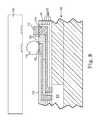
- FIG. 2illustrates printed layer 56 printed to top surface 58 of the substrate 52 and at locations 60 between IC terminal 54 .
- the cover layer 56overlaps edges 62 the IC device 50 and helps to retain it in recess 64 in the substrate 52 .
- the printed layer 56 at locations 60creates one or more recesses 66 corresponding to each of the IC terminals 54 that are used in subsequent steps of the process.
- the recesses 66 for the IC terminals 54are metalized to create contact members 70 .
- Metalizingcan be performed by printing conductive particles followed by a sintering step, by printing conductive inks, or a variety of other techniques.
- the metalizing materialis preferably of copper or similar metallic materials such as phosphor bronze or beryllium-copper.
- the resulting contact members 70are optionally plated to improve conductive properties.
- the platingis preferably a corrosion resistant metallic material such as nickel, gold, silver, palladium, or multiple layers thereof.
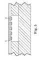
- dielectric layer 72is printed on surface 74 with recesses 76 corresponding to a desired circuit geometry.
- the dielectric layer 72is placed on surface 74 .
- the recesses 76can be defined by printing, embossing, imprinting, chemical etching with a printed mask, or a variety of other techniques.
- the recesses 76are metalized as discussed above to create circuit geometry 78 .
- the circuit geometry 78is formed by depositing a conductive material in a first state in the recesses 76 , and then processed to create a second more permanent state.
- the metallic powderis printed according to the circuit geometry and subsequently sintered, or the curable conductive material flows into the circuit geometry and is subsequently cured.
- curable and inflections thereofrefers to a chemical-physical transformation that allows a material to progress from a first form (e.g., flowable form) to a more permanent second form.
- “Curable”refers to an uncured material having the potential to be cured, such as for example by the application of a suitable energy source.
- the recesses 66 , 76 in the layers 56 , 72 , 82 , 84 , 86permit control of the location, cross section, material content, and aspect ratio of the contact members 70 and the conductive traces in the circuit geometry 78 . Maintaining the conductive traces with a cross-section of 1:1 or greater provides greater signal integrity than traditional subtractive trace forming technologies. For example, traditional methods take a sheet of a given thickness and etches the material between the traces away to have a resultant trace that is usually wider than it is thick. The etching process also removes more material at the top surface of the trace than at the bottom, leaving a trace with a trapezoidal cross-sectional shape, degrading signal integrity in some applications. Using the recesses 66 , 76 to control the aspect ratio of the conductive traces results in a more rectangular or square cross-section of the conductive traces in the circuit geometry 78 , with the corresponding improvement in signal integrity.
- pre-patterned or pre-etched thin conductive foil circuit tracesare transferred to the recesses 66 , 76 .
- a pressure sensitive adhesivecan be used to retain the copper foil circuit traces in the recesses 66 , 76 .
- the trapezoidal cross-sections of the pre-formed conductive foil tracesare then post-plated.
- the plating materialfills the open spaces in the recesses 66 , 76 not occupied by the foil circuit geometry, resulting in a substantially rectangular or square cross-sectional shape corresponding to the shape of the recesses 66 , 76 .
- a thin conductive foilis pressed into the recesses 64 , 76 , and the edges of the recesses 66 , 76 act to cut or shear the conductive foil.
- the processlocates a portion of the conductive foil in the trenches 66 , 76 , but leaves the negative pattern of the conductive foil not wanted outside and above the trenches 66 , 76 for easy removal.
- the foil in the trenches 66 , 76is preferably post plated to add material to increase the thickness of the conductive traces in the circuit geometry 78 and to fill any voids left between the conductive foil and the recesses 66 , 76 .
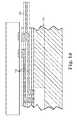
- FIG. 6illustrates additional printed dielectric layers 80 , 82 , 84 , 86 creating additional recesses that are metalized to extend the circuit geometry 78 .
- the dielectric layer 56 , 72 , 80 , 82 , 84 , 86may be constructed of any of a number of dielectric materials that provide electrostatic dissipation or to reduce cross-talk between the traces of the circuit geometry 62 .
- An efficient way to prevent electrostatic discharge (“ESD”)is to construct one of the layers from materials that are not too conductive but that will slowly conduct static charges away. These materials preferably have resistivity values in the range of 10 5 to 10 11 Ohm-meters.
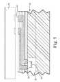
- FIG. 7illustrates the circuit geometry 78 routing the IC terminals 54 out of semiconductor package 90 .
- the size and pitch of exposed terminals 92are printed to electrically couple the IC device 50 to another circuit member 94 , such as a printed circuit board or a socket.
- the semiconductor package 90permits fine contact-to-contact spacing 96 (pitch) on the order of less than 1.0 mm pitch, and more preferably a pitch of less than about 0.7 millimeter, and most preferably a pitch of less than about 0.4 millimeter.
- the present semiconductor package 90permits the performance of the IC device 50 to be evaluated before being incorporated into a system in package or multi-chip module before final packaging, permitting the individual die to be replaced if necessary.
- the additive process disclosed hereinalso permits the circuit geometry 78 to be written directly on the IC device 50 , without the need of the intermediate die bonding step.
- FIG. 8illustrates an alternate semiconductor package 100 with modified terminals 102 , 104 in accordance with an embodiment of the present disclosure.
- Resilient regions 106are preferably printed during the creation of layers 108 .
- dielectric materialis printed to leave a recess into which the resilient materials are deposited, preferably by printing.
- the resilient regions 106permit the terminals 102 , 104 to move in all six degrees of freedom (X-Y-Z-Pitch-Roll-Yaw) to facilitate electrical coupling with circuit member 116 .
- the resilient regions 106increase the compliance of the modified terminals to permit electrical coupling by compression, without the need to solder the semiconductor package 100 .
- the semiconductor package 100permits IC device 118 to be tested prior to final packaging, dramatically improving yields.
- solder ball 110is located on terminal 102 .
- conductive material 112is printed on the terminal so it extends above surface 114 of the semiconductor package 100 .
- circuit membersrefers to, for example, a packaged integrated circuit device, an unpackaged integrated circuit device, a printed circuit board, a flexible circuit, a bare-die device, an organic or inorganic substrate, a rigid circuit, or any other device capable of carrying electrical current.
- FIG. 9illustrates an alternate semiconductor package 120 with printed electrical devices 122 in accordance with an embodiment of the present disclosure.
- the electrical devices 122can include passive or active functional elements.
- Passive structurerefers to a structure having a desired electrical, magnetic, or other property, including but not limited to a conductor, resistor, capacitor, inductor, insulator, dielectric, suppressor, filter, varistor, ferromagnet, and the like.
- the electrical devices 122are preferably printed during construction of the semiconductor package 120 .
- the electrical devices 122can be ground planes, power planes, electrical connections to other circuit members, dielectric layers, conductive traces, transistors, capacitors, resistors, RF antennae, shielding, filters, signal or power altering and enhancing devices, memory devices, embedded IC, and the like.
- the electrical devices 122can be formed using printing technology, adding intelligence to the semiconductor package 120 .
- Features that are typically located on the IC device 124can be incorporated into the semiconductor package 120 in accordance with an embodiment of the present disclosure.
- 6,750,473(Amundson et al.), which are incorporated by reference, teach using ink-jet printing to make various electrical devices, such as, resistors, capacitors, diodes, inductors (or elements which may be used in radio applications or magnetic or electric field transmission of power or data), semiconductor logic elements, electro-optical elements, transistor (including, light emitting, light sensing or solar cell elements, field effect transistor, top gate structures), and the like.
- the electrical devices 202can also be created by aerosol printing, such as disclosed in U.S. Pat. No. 7,674,671 (Renn et al.); U.S. Pat. No. 7,658,163 (Renn et al.); U.S. Pat. No. 7,485,345 (Renn et al.); U.S. Pat. No. 7,045,015 (Renn et al.); and U.S. Pat. No. 6,823,124 (Renn et al.), which are hereby incorporated by reference.
- Printing processesare preferably used to fabricate various functional structures, such as conductive paths and electrical devices, without the use of masks or resists.
- Features down to about 10 micronscan be directly written in a wide variety of functional inks, including metals, ceramics, polymers and adhesives, on virtually any substrate—silicon, glass, polymers, metals and ceramics.
- the substratescan be planar and non-planar surfaces.
- the printing processis typically followed by a thermal treatment, such as in a furnace or with a laser, to achieve dense functionalized structures.
- Ink jet printing of electronically active inkscan be done on a large class of substrates, without the requirements of standard vacuum processing or etching.
- the inksmay incorporate mechanical, electrical or other properties, such as, conducting, insulating, resistive, magnetic, semi conductive, light modulating, piezoelectric, spin, optoelectronic, thermoelectric or radio frequency.
- a plurality of ink dropsare dispensed from the print head directly to a substrate or on an intermediate transfer member.
- the transfer membercan be a planar or non-planar structure, such as a drum.
- the surface of the transfer membercan be coated with a non-sticking layer, such as silicone, silicone rubber, or Teflon.
- the ink(also referred to as function inks) can include conductive materials, semi-conductive materials (e.g., p-type and n-type semiconducting materials), metallic material, insulating materials, and/or release materials.
- the ink patterncan be deposited in precise locations on a substrate to create fine lines having a width smaller than 10 microns, with precisely controlled spaces between the lines.
- the ink dropsform an ink pattern corresponding to portions of a transistor, such as a source electrode, a drain electrode, a dielectric layer, a semiconductor layer, or a gate electrode.
- the substratecan be an insulating polymer, such as polyethylene terephthalate (PET), polyester, polyethersulphone (PES), polyimide film (e.g. Kapton, available from DuPont located in Wilmington, Del.; Upilex available from Ube Corporation located in Japan), or polycarbonate.
- PETpolyethylene terephthalate
- PETpolyethylene terephthalate
- PETpolyethersulphone
- polyimide filme.g. Kapton, available from DuPont located in Wilmington, Del.; Upilex available from Ube Corporation located in Japan
- polycarbonatee.g. Kapton, available from DuPont located in Wilmington, Del.; Upilex available from Ube Corporation located in Japan
- the substratecan be made of an insulator such as undoped silicon, glass, or a plastic material.
- the substratecan also be patterned to serve as an electrode.
- the substratecan further be a metal foil insulated from the gate electrode by a non-conducting material.
- the substratecan also be
- Electrodescan be printed with metals, such as aluminum or gold, or conductive polymers, such as polythiophene or polyaniline.
- the electrodesmay also include a printed conductor, such as a polymer film comprising metal particles, such as silver or nickel, a printed conductor comprising a polymer film containing graphite or some other conductive carbon material, or a conductive oxide such as tin oxide or indium tin oxide.
- Dielectric layerscan be printed with a silicon dioxide layer, an insulating polymer, such as polyimide and its derivatives, poly-vinyl phenol, polymethylmethacrylate, polyvinyldenedifluoride, an inorganic oxide, such as metal oxide, an inorganic nitride such as silicon nitride, or an inorganic/organic composite material such as an organic-substituted silicon oxide, or a sol-gel organosilicon glass.
- Dielectric layerscan also include a bicylcobutene derivative (BCB) available from Dow Chemical (Midland, Mich.), spin-on glass, or dispersions of dielectric colloid materials in a binder or solvent.
- BCBbicylcobutene derivative
- Semiconductor layerscan be printed with polymeric semiconductors, such as, polythiophene, poly(3-alkyl)thiophenes, alkyl-substituted oligothiophene, polythienylenevinylene, poly(para-phenylenevinylene) and doped versions of these polymers.
- polymeric semiconductorssuch as, polythiophene, poly(3-alkyl)thiophenes, alkyl-substituted oligothiophene, polythienylenevinylene, poly(para-phenylenevinylene) and doped versions of these polymers.
- An example of suitable oligomeric semiconductoris alpha-hexathienylene. Horowitz, Organic Field-Effect Transistors, Adv. Mater., 10, No. 5, p. 365 (1998) describes the use of unsubstituted and alkyl-substituted oligothiophenes in transistors.
- a field effect transistor made with regioregular poly(3-hexylthiophene) as the semiconductor layeris described in Bao et al., Soluble and Processable Regioregular Poly(3-hexylthiophene) for Thin Film Field-Effect Transistor Applications with High Mobility, Appl. Phys. Lett. 69 (26), p. 4108 (December 1996).
- a field effect transistor made with a-hexathienyleneis described in U.S. Pat. No. 5,659,181, which is incorporated herein by reference.
- a protective layercan optionally be printed onto the electrical devices.
- the protective layercan be an aluminum film, a metal oxide coating, a substrate, or a combination thereof.
- Organic semiconductorscan be printed using suitable carbon-based compounds, such as, pentacene, phthalocyanine, benzodithiophene, buckminsterfullerene or other fullerene derivatives, tetracyanonaphthoquinone, and tetrakisimethylanimoethylene.
- suitable carbon-based compoundssuch as, pentacene, phthalocyanine, benzodithiophene, buckminsterfullerene or other fullerene derivatives, tetracyanonaphthoquinone, and tetrakisimethylanimoethylene.
- suitable carbon-based compoundssuch as, pentacene, phthalocyanine, benzodithiophene, buckminsterfullerene or other fullerene derivatives, tetracyanonaphthoquinone, and tetrakisimethylanimoethylene.
- the ink-jet print headpreferably includes a plurality of orifices for dispensing one or more fluids onto a desired media, such as for example, a conducting fluid solution, a semiconducting fluid solution, an insulating fluid solution, and a precursor material to facilitate subsequent deposition.
- a desired mediasuch as for example, a conducting fluid solution, a semiconducting fluid solution, an insulating fluid solution, and a precursor material to facilitate subsequent deposition.
- the precursor materialcan be surface active agents, such as octadecyltrichlorosilane (OTS).
- a separate print headis used for each fluid solution.
- the print head nozzlescan be held at different potentials to aid in atomization and imparting a charge to the droplets, such as disclosed in U.S. Pat. No. 7,148,128 (Jacobson), which is hereby incorporated by reference.
- Alternate print headsare disclosed in U.S. Pat. No. 6,626,526 (Ueki et al.), and U.S. Pat. Publication Nos. 2006/0044357 (Andersen et al.) and 2009/0061089 (King et al.), which are hereby incorporated by reference.
- the print headpreferably uses a pulse-on-demand method, and can employ one of the following methods to dispense the ink drops: piezoelectric, magnetostrictive, electromechanical, electro pneumatic, electrostatic, rapid ink heating, magneto hydrodynamic, or any other technique well known to those skilled in the art.
- the deposited ink patternstypically undergo a curing step or another processing step before subsequent layers are applied.
- printingis intended to include all forms of printing and coating, including: pre-metered coating such as patch die coating, slot or extrusion coating, slide or cascade coating, and curtain coating; roll coating such as knife over roll coating, forward and reverse roll coating; gravure coating; dip coating; spray coating; meniscus coating; spin coating; brush coating; air knife coating; screen printing processes; electrostatic printing processes; thermal printing processes; and other similar techniques.
- pre-metered coatingsuch as patch die coating, slot or extrusion coating, slide or cascade coating, and curtain coating
- roll coatingsuch as knife over roll coating, forward and reverse roll coating
- gravure coatingdip coating
- spray coatingmeniscus coating
- spin coatingspin coating
- brush coatingair knife coating
- screen printing processeselectrostatic printing processes
- thermal printing processesand other similar techniques.
- FIG. 10illustrates an alternate semiconductor package 140 with external routing 142 in accordance with an embodiment of the present disclosure.
- the external routing 142is preferably an extension of circuit geometer 144 made using the printing technology discussed above.
- the external routing 142can be constructed to accommodate connection to desired functions, such as for example, power management and delivery, tester interface, functional display or indicators, and the like.
- FIG. 11illustrates a semiconductor package 150 that simulates a system in package (SIP) or multichip module format, in accordance with an embodiment of the present disclosure.
- Multiple IC devices 152 , 154are located in the semiconductor package 150 .
- Dielectric layers 156 and circuit geometry 158are printed as discussed above.
- the circuit geometry 158permits inter-die circuit paths 160 and intra-die circuit paths 162 .
- Contact pads 164can be configured in a variety of ways to couple with circuit member 166 .
- FIG. 12illustrates a semiconductor package 170 with stacked IC devices 172 , 174 in accordance with an embodiment of the present disclosure.
- Through silicon vias 176permit contact pads 178 on IC device 172 to electrically couple with circuit geometry 180 and/or IC device 174 .
- the through silicon vias 176eliminate edge wiring and permit a shorter vertical stack.
- the through silicon vias 176can be formed using the printing processes discussed herein or other methods.
- FIG. 13illustrates an alternate semiconductor package 200 in accordance with an embodiment of the present disclosure.
- RF shielding 202is optionally printed in recess 204 of substrate 206 .
- substrate 206is optimized for thermal management.
- IC device 208is retained to substrate 206 by overmolding or encapsulation 210 .
- Dielectric layers 212 and circuit geometry 214are preferably printed as discussed above.
- the circuit geometry 214is configured to add additional IC device 216 in a double sided configuration.
- the semiconductor package 200can be mated with another assembly to create a complex system in package or multichip module.
Landscapes
- Engineering & Computer Science (AREA)
- Computer Hardware Design (AREA)
- Microelectronics & Electronic Packaging (AREA)
- Power Engineering (AREA)
- Physics & Mathematics (AREA)
- Condensed Matter Physics & Semiconductors (AREA)
- General Physics & Mathematics (AREA)
- Manufacturing & Machinery (AREA)
- Manufacturing Of Printed Wiring (AREA)
- Structures Or Materials For Encapsulating Or Coating Semiconductor Devices Or Solid State Devices (AREA)
Abstract
Description
The present application is a divisional application of U.S. Ser. No. 13/318,263, entitled Compliant Printed Circuit Semiconductor Package, filed Oct. 31, 2011 (Allowed), which is a section 371 application of PCT/U.S.2010/36285, entitled Compliant Printed Circuit Semiconductor Package, filed May 27, 2010, which claims the benefit of U.S. Provisional Application No. 61/183,348, entitled Compliant Printed Circuit Known Good Die (KGD) Vehicle or Semiconductor Package, filed Jun. 2, 2009, the entire disclosures of which are hereby incorporated by reference.
The present application is directed to a simulated or actual semiconductor package that leverages the capabilities of additive printing processes to provide a high performance package capable of interconnecting single or multiple devices in a permanent or separable fashion.
Traditional semiconductors and IC devices are typically packaged in a variety of ways to provide redistribution from the terminals on the die to a spacing that is conducive to cost effective printed circuit board (“PCB”) fabrication techniques. In many cases, the size and distance between die terminals is so small that the device cannot be connected to the final PCB without some sort of fan out or routing. The packages also serve to protect the fragile silicon or provide additional functions such as thermal management or near device decoupling. In many cases, the size and distance between die terminals is so small that the IC device cannot be connected to the final PCB without some sort of re-routing interface.
Most IC devices are produced with terminals in either a peripheral pattern that runs along the edges of the IC device or an area array pattern that spans across the surface of the IC device. A main method for attachment when the terminals are in an area array pattern is to connect the terminals with solder. Basically, the package has an array of terminals that correspond to the IC device terminals. Solder is applied the terminals on the IC device and/or the package and reflowed to create the mechanical and electrical connection in a process commonly called flip chip attachment. In a flip chip attachment the IC device is flipped over to mate the terminals on the die to the terminals on the IC package substrate.
The IC devices in these types of packages are often under filled with an epoxy of some type to provide support and strength to the solder joints. The epoxy protects the solder joints during use from thermal expansion, miss-match and/or shock. In both cases, the connection of the IC device to the package is generally not reworkable once packaged and if there is a missing or broken connection it is difficult to repair.
Once the IC devices are packaged, they are usually tested in a variety of ways to determine the reliability and performance of the IC devices in the package as they would be used in the final application. In many cases, the functional performance of the IC device is not known prior to placing it into the package and if the packaged IC device fails testing the cost of the package and processing is lost.
Area array packaging has been utilized for many years, and provides a method for interconnecting IC devices with larger terminal counts than peripheral lead packaging. In general, the area array packaging is more expensive due to the larger pin counts and more sophisticated substrates required. The main limitations for area array packaging are the terminal pitch, thermal management, cost, ability to rework faulty IC devices and reliability of the solder joints.
There also have been advancements in recent years in both package types where multiple IC devices are placed in the same package, creating what has been nicknamed SiP or “system in package”. Placing multiple IC devices in a single package further complicates the problems discussed above.
The present disclosure is directed to providing a simulated or actual semiconductor package that leverages the capabilities of additive printing processes to provide a high performance package capable of interconnecting a single or multiple IC devices in a permanent or separable fashion. The present semiconductor package preferably permits the IC devices to be tested prior to final packaging.
The present compliant printed circuit semiconductor package resembles a traditional package in construction, but utilizes additive printing processes rather than conventional subtractive processes. The unique nature of the additive printing processes allows for a direct writing of circuitry and dielectrics, with the added benefit of stress decoupling at the terminal joints as well as embedded function not seen in traditional packaging.
The use of additive printing processes permits the material set in a given layer to vary. Traditional PCB and flex circuit fabrication methods take sheets of material and stack them up, laminate, and/or drill. The materials in each layer are limited to the materials in a particular sheet. Additive printing technologies permit a wide variety of materials to be applied on a layer with a registration relative to the features of the previous layer. Selective addition of conductive, non-conductive, or semi-conductive materials at precise locations to create a desired effect has the major advantages in tuning impedance or adding electrical function on a given layer. Tuning performance on a layer by layer basis relative to the previous layer greatly enhances electrical performance.
One embodiment is directed to a package for at least one semiconductor device and a method for making the package. At least one dielectric layer is selectively printed on at least a portion of the semiconductor device creating first recesses aligned with a plurality of the electrical terminals. A conductive material is printed in the first recesses forming contact members on the semiconductor device. At least one dielectric layer is selectively printed on at least a portion of the package to create a plurality of second recesses corresponding to a target circuit geometry. A conductive material is printed in at least a portion of the second recesses to create a circuit geometry. The circuit geometry includes a plurality of exposed terminals electrically coupled to the electric terminals on the semiconductor device.
Conductive plating is preferably added to one or more of the contact members and the circuit geometry. The conductive material can be sintered conductive particles or a conductive ink. In one embodiment, a compliant material is located between the exposed terminals and the substrate. In another embodiment, at least one electrical device is printed on one of a dielectric layer or the substrate and electrically coupled to at least a portion of the circuit geometry. The exposed terminals preferably extend above the package.
The resulting circuit geometry preferably has conductive traces that have substantially rectangular cross-sectional shapes, corresponding to the second recesses. The use of additive printing processes permit conductive material, non-conductive material, and semi-conductive material to be located on a single layer.
In one embodiment, pre-formed conductive trace materials are located in the second recesses. The second recesses are than plated to form conductive traces with substantially rectangular cross-sectional shapes. In another embodiment, a conductive foil is pressed into at least a portion of the second recesses. The conductive foil is sheared along edges of the second recesses. The excess conductive foil not located in the second recesses is removed and the second recesses are plated to form conductive traces with substantially rectangular cross-sectional shapes.
In another embodiment, at least one external dielectric layer extends beyond the package. External routing is printed on the external dielectric layer and electrically coupled to a portion of the circuit geometry.
The package can include a plurality of semiconductor devices. The circuit geometry may include at least one of an inter-die circuit path or an intra-die circuit paths. The semiconductor devices are optionally arranged in a stacked configuration.
The present disclosure is also directed to an electrical assembly including a circuit member with a plurality of contact pads electrically coupled to the exposed terminals on the package. The circuit member can be selected from one of a dielectric layer, a printed circuit board, a flexible circuit, a bare die device, an integrated circuit device, organic or inorganic substrates, or a rigid circuit.
This present compliant printed semiconductor package enables internal and/or external compliance to enhance the mechanical performance of the circuit. The present semiconductor package can be produced digitally, without tooling or costly artwork. The semiconductor package can be produced as a “Green” product, with dramatic reductions in environmental issues related to the production of conventional semiconductor packages.
The present disclosure is also directed to several additive processes that combine the mechanical or structural properties of a polymer material, while adding metal materials in an unconventional fashion, to create electrical paths that are refined to provide electrical performance improvements. By adding or arranging metallic particles, conductive inks, plating, or portions of traditional alloys, the compliant printed semiconductor package reduces parasitic electrical effects and impedance mismatch, potentially increasing the current carrying capacity.
The printing process permits the fabrication of functional structures, such as conductive paths and electrical devices, without the use of masks or resists. Features down to about 10 microns can be directly written in a wide variety of functional inks, including metals, ceramics, polymers and adhesives, on virtually any substrate—silicon, glass, polymers, metals and ceramics. The substrates can be planar and non-planar surfaces. The printing process is typically followed by a thermal treatment, such as in a furnace or with a laser, to achieve dense functionalized structures.
The compliant printed semiconductor package can be configured with conductive traces that reduce or redistribute the terminal pitch, without the addition of an interposer or daughter substrate. Grounding schemes, shielding, electrical devices, and power planes can be added to the semiconductor package, reducing the number of connections to the PCB and relieving routing constraints while increasing performance.
The present disclosure is also directed to a method of making a package for a semiconductor device having electrical terminals. The method includes locating at least one semiconductor device on a substrate. A first dielectric layer is printed on at least a portion of the semiconductor device to include first recesses aligned with a plurality of the electrical terminals. A conductive material is deposited in the first recesses forming contact members on the semiconductor device. A second dielectric layer is printed on at least a portion of the first dielectric layer to include second recesses aligned with a plurality of the first recesses. A conductive material is deposited in at least a portion of the second recesses to include a circuit geometry. The circuit geometry includes a plurality of exposed terminals. A compliant material is deposited in recesses in one or more of the first and second dielectric layers adjacent to a plurality of the exposed terminals to permit the exposed terminals to move within the dielectric layers relative to the substrate.
As illustrated inFIG. 3 , therecesses 66 for theIC terminals 54 are metalized to createcontact members 70. Metalizing can be performed by printing conductive particles followed by a sintering step, by printing conductive inks, or a variety of other techniques. The metalizing material is preferably of copper or similar metallic materials such as phosphor bronze or beryllium-copper. The resultingcontact members 70 are optionally plated to improve conductive properties. The plating is preferably a corrosion resistant metallic material such as nickel, gold, silver, palladium, or multiple layers thereof.
As illustrated inFIG. 4 ,dielectric layer 72 is printed onsurface 74 withrecesses 76 corresponding to a desired circuit geometry. Alternatively, thedielectric layer 72 is placed onsurface 74. Therecesses 76 can be defined by printing, embossing, imprinting, chemical etching with a printed mask, or a variety of other techniques. As illustrated inFIG. 5 , therecesses 76 are metalized as discussed above to createcircuit geometry 78.
In one embodiment, thecircuit geometry 78 is formed by depositing a conductive material in a first state in therecesses 76, and then processed to create a second more permanent state. For example, the metallic powder is printed according to the circuit geometry and subsequently sintered, or the curable conductive material flows into the circuit geometry and is subsequently cured. As used herein “cure” and inflections thereof refers to a chemical-physical transformation that allows a material to progress from a first form (e.g., flowable form) to a more permanent second form. “Curable” refers to an uncured material having the potential to be cured, such as for example by the application of a suitable energy source.
Therecesses layers contact members 70 and the conductive traces in thecircuit geometry 78. Maintaining the conductive traces with a cross-section of 1:1 or greater provides greater signal integrity than traditional subtractive trace forming technologies. For example, traditional methods take a sheet of a given thickness and etches the material between the traces away to have a resultant trace that is usually wider than it is thick. The etching process also removes more material at the top surface of the trace than at the bottom, leaving a trace with a trapezoidal cross-sectional shape, degrading signal integrity in some applications. Using therecesses circuit geometry 78, with the corresponding improvement in signal integrity.
In another embodiment, pre-patterned or pre-etched thin conductive foil circuit traces are transferred to therecesses recesses recesses recesses
In another embodiment, a thin conductive foil is pressed into therecesses recesses trenches trenches trenches circuit geometry 78 and to fill any voids left between the conductive foil and therecesses
Thepresent semiconductor package 90 permits the performance of theIC device 50 to be evaluated before being incorporated into a system in package or multi-chip module before final packaging, permitting the individual die to be replaced if necessary. The additive process disclosed herein also permits thecircuit geometry 78 to be written directly on theIC device 50, without the need of the intermediate die bonding step.
Theresilient regions 106 increase the compliance of the modified terminals to permit electrical coupling by compression, without the need to solder thesemiconductor package 100. Thesemiconductor package 100permits IC device 118 to be tested prior to final packaging, dramatically improving yields. In one embodiment,solder ball 110 is located onterminal 102. In another embodiment,conductive material 112 is printed on the terminal so it extends abovesurface 114 of thesemiconductor package 100.
The embodiment ofFIG. 8 can be pressed againstcircuit member 116 and powered without the need for a socket. Alternatively, thesemiconductor package 100 can be inserted into an LGA or BGA socket, or soldered tocircuit member 116. As used herein, the term “circuit members” refers to, for example, a packaged integrated circuit device, an unpackaged integrated circuit device, a printed circuit board, a flexible circuit, a bare-die device, an organic or inorganic substrate, a rigid circuit, or any other device capable of carrying electrical current.
Theelectrical devices 122 are preferably printed during construction of thesemiconductor package 120. Theelectrical devices 122 can be ground planes, power planes, electrical connections to other circuit members, dielectric layers, conductive traces, transistors, capacitors, resistors, RF antennae, shielding, filters, signal or power altering and enhancing devices, memory devices, embedded IC, and the like. For example, theelectrical devices 122 can be formed using printing technology, adding intelligence to thesemiconductor package 120. Features that are typically located on theIC device 124 can be incorporated into thesemiconductor package 120 in accordance with an embodiment of the present disclosure.
The availability of printable silicon inks provides the ability to printelectrical devices 122, such as disclosed in U.S. Pat. No. 7,485,345 (Renn et al.); U.S. Pat. No. 7,382,363 (Albert et al.); U.S. Pat. No. 7,148,128 (Jacobson); U.S. Pat. No. 6,967,640 (Albert et al.); U.S. Pat. No. 6,825,829 (Albert et al.); U.S. Pat. No. 6,750,473 (Amundson et al.); U.S. Pat. No. 6,652,075 (Jacobson); U.S. Pat. No. 6,639,578 (Comiskey et al.); U.S. Pat. No. 6,545,291 (Amundson et al.); U.S. Pat. No. 6,521,489 (Duthaler et al.); U.S. Pat. No. 6,459,418 (Comiskey et al.); U.S. Pat. No. 6,422,687 (Jacobson); U.S. Pat. No. 6,413,790 (Duthaler et al.); U.S. Pat. No. 6,312,971 (Amundson et al.); U.S. Pat. No. 6,252,564 (Albert et al.); U.S. Pat. No. 6,177,921 (Comiskey et al.); U.S. Pat. No. 6,120,588 (Jacobson); U.S. Pat. No. 6,118,426 (Albert et al.); and U.S. Pat. Publication No. 2008/0008822 (Kowalski et al.), which are hereby incorporated by reference. In particular, U.S. Pat. No. 6,506,438 (Duthaler et al.) and U.S. Pat. No. 6,750,473 (Amundson et al.), which are incorporated by reference, teach using ink-jet printing to make various electrical devices, such as, resistors, capacitors, diodes, inductors (or elements which may be used in radio applications or magnetic or electric field transmission of power or data), semiconductor logic elements, electro-optical elements, transistor (including, light emitting, light sensing or solar cell elements, field effect transistor, top gate structures), and the like.
Theelectrical devices 202 can also be created by aerosol printing, such as disclosed in U.S. Pat. No. 7,674,671 (Renn et al.); U.S. Pat. No. 7,658,163 (Renn et al.); U.S. Pat. No. 7,485,345 (Renn et al.); U.S. Pat. No. 7,045,015 (Renn et al.); and U.S. Pat. No. 6,823,124 (Renn et al.), which are hereby incorporated by reference.
Printing processes are preferably used to fabricate various functional structures, such as conductive paths and electrical devices, without the use of masks or resists. Features down to about 10 microns can be directly written in a wide variety of functional inks, including metals, ceramics, polymers and adhesives, on virtually any substrate—silicon, glass, polymers, metals and ceramics. The substrates can be planar and non-planar surfaces. The printing process is typically followed by a thermal treatment, such as in a furnace or with a laser, to achieve dense functionalized structures.
Ink jet printing of electronically active inks can be done on a large class of substrates, without the requirements of standard vacuum processing or etching. The inks may incorporate mechanical, electrical or other properties, such as, conducting, insulating, resistive, magnetic, semi conductive, light modulating, piezoelectric, spin, optoelectronic, thermoelectric or radio frequency.
In one embodiment, a plurality of ink drops are dispensed from the print head directly to a substrate or on an intermediate transfer member. The transfer member can be a planar or non-planar structure, such as a drum. The surface of the transfer member can be coated with a non-sticking layer, such as silicone, silicone rubber, or Teflon.
The ink (also referred to as function inks) can include conductive materials, semi-conductive materials (e.g., p-type and n-type semiconducting materials), metallic material, insulating materials, and/or release materials. The ink pattern can be deposited in precise locations on a substrate to create fine lines having a width smaller than 10 microns, with precisely controlled spaces between the lines. For example, the ink drops form an ink pattern corresponding to portions of a transistor, such as a source electrode, a drain electrode, a dielectric layer, a semiconductor layer, or a gate electrode.
The substrate can be an insulating polymer, such as polyethylene terephthalate (PET), polyester, polyethersulphone (PES), polyimide film (e.g. Kapton, available from DuPont located in Wilmington, Del.; Upilex available from Ube Corporation located in Japan), or polycarbonate. Alternatively, the substrate can be made of an insulator such as undoped silicon, glass, or a plastic material. The substrate can also be patterned to serve as an electrode. The substrate can further be a metal foil insulated from the gate electrode by a non-conducting material. The substrate can also be a woven material or paper, planarized or otherwise modified on at least one surface by a polymeric or other coating to accept the other structures.
Electrodes can be printed with metals, such as aluminum or gold, or conductive polymers, such as polythiophene or polyaniline. The electrodes may also include a printed conductor, such as a polymer film comprising metal particles, such as silver or nickel, a printed conductor comprising a polymer film containing graphite or some other conductive carbon material, or a conductive oxide such as tin oxide or indium tin oxide.
Dielectric layers can be printed with a silicon dioxide layer, an insulating polymer, such as polyimide and its derivatives, poly-vinyl phenol, polymethylmethacrylate, polyvinyldenedifluoride, an inorganic oxide, such as metal oxide, an inorganic nitride such as silicon nitride, or an inorganic/organic composite material such as an organic-substituted silicon oxide, or a sol-gel organosilicon glass. Dielectric layers can also include a bicylcobutene derivative (BCB) available from Dow Chemical (Midland, Mich.), spin-on glass, or dispersions of dielectric colloid materials in a binder or solvent.
Semiconductor layers can be printed with polymeric semiconductors, such as, polythiophene, poly(3-alkyl)thiophenes, alkyl-substituted oligothiophene, polythienylenevinylene, poly(para-phenylenevinylene) and doped versions of these polymers. An example of suitable oligomeric semiconductor is alpha-hexathienylene. Horowitz, Organic Field-Effect Transistors, Adv. Mater., 10, No. 5, p. 365 (1998) describes the use of unsubstituted and alkyl-substituted oligothiophenes in transistors. A field effect transistor made with regioregular poly(3-hexylthiophene) as the semiconductor layer is described in Bao et al., Soluble and Processable Regioregular Poly(3-hexylthiophene) for Thin Film Field-Effect Transistor Applications with High Mobility, Appl. Phys. Lett. 69 (26), p. 4108 (December 1996). A field effect transistor made with a-hexathienylene is described in U.S. Pat. No. 5,659,181, which is incorporated herein by reference.
A protective layer can optionally be printed onto the electrical devices. The protective layer can be an aluminum film, a metal oxide coating, a substrate, or a combination thereof.
Organic semiconductors can be printed using suitable carbon-based compounds, such as, pentacene, phthalocyanine, benzodithiophene, buckminsterfullerene or other fullerene derivatives, tetracyanonaphthoquinone, and tetrakisimethylanimoethylene. The materials provided above for forming the substrate, the dielectric layer, the electrodes, or the semiconductor layer are exemplary only. Other suitable materials known to those skilled in the art having properties similar to those described above can be used in accordance with the present disclosure.
The ink-jet print head preferably includes a plurality of orifices for dispensing one or more fluids onto a desired media, such as for example, a conducting fluid solution, a semiconducting fluid solution, an insulating fluid solution, and a precursor material to facilitate subsequent deposition. The precursor material can be surface active agents, such as octadecyltrichlorosilane (OTS).
Alternatively, a separate print head is used for each fluid solution. The print head nozzles can be held at different potentials to aid in atomization and imparting a charge to the droplets, such as disclosed in U.S. Pat. No. 7,148,128 (Jacobson), which is hereby incorporated by reference. Alternate print heads are disclosed in U.S. Pat. No. 6,626,526 (Ueki et al.), and U.S. Pat. Publication Nos. 2006/0044357 (Andersen et al.) and 2009/0061089 (King et al.), which are hereby incorporated by reference.
The print head preferably uses a pulse-on-demand method, and can employ one of the following methods to dispense the ink drops: piezoelectric, magnetostrictive, electromechanical, electro pneumatic, electrostatic, rapid ink heating, magneto hydrodynamic, or any other technique well known to those skilled in the art. The deposited ink patterns typically undergo a curing step or another processing step before subsequent layers are applied.
While ink jet printing is preferred, the term “printing” is intended to include all forms of printing and coating, including: pre-metered coating such as patch die coating, slot or extrusion coating, slide or cascade coating, and curtain coating; roll coating such as knife over roll coating, forward and reverse roll coating; gravure coating; dip coating; spray coating; meniscus coating; spin coating; brush coating; air knife coating; screen printing processes; electrostatic printing processes; thermal printing processes; and other similar techniques.
Where a range of values is provided, it is understood that each intervening value, to the tenth of the unit of the lower limit unless the context clearly dictates otherwise, between the upper and lower limit of that range and any other stated or intervening value in that stated range is encompassed within the embodiments of the disclosure. The upper and lower limits of these smaller ranges which may independently be included in the smaller ranges is also encompassed within the embodiments of the disclosure, subject to any specifically excluded limit in the stated range. Where the stated range includes one or both of the limits, ranges excluding either both of those included limits are also included in the embodiments of the present disclosure.
Unless defined otherwise, all technical and scientific terms used herein have the same meaning as commonly understood by one of ordinary skill in the art to which the embodiments of the present disclosure belong. Although any methods and materials similar or equivalent to those described herein can also be used in the practice or testing of the embodiments of the present disclosure, the preferred methods and materials are now described. All patents and publications mentioned herein, including those cited in the Background of the application, are hereby incorporated by reference to disclose and described the methods and/or materials in connection with which the publications are cited.
The publications discussed herein are provided solely for their disclosure prior to the filing date of the present application. Nothing herein is to be construed as an admission that the present disclosure is not entitled to antedate such publication by virtue of prior invention. Further, the dates of publication provided may be different from the actual publication dates which may need to be independently confirmed.
Other embodiments of the disclosure are possible. Although the description above contains much specificity, these should not be construed as limiting the scope of the disclosure, but as merely providing illustrations of some of the presently preferred embodiments of this disclosure. It is also contemplated that various combinations or sub-combinations of the specific features and aspects of the embodiments may be made and still fall within the scope of the present disclosure. It should be understood that various features and aspects of the disclosed embodiments can be combined with or substituted for one another in order to form varying modes of the disclosed embodiments of the disclosure. Thus, it is intended that the scope of the present disclosure herein disclosed should not be limited by the particular disclosed embodiments described above.
Thus the scope of this disclosure should be determined by the appended claims and their legal equivalents. Therefore, it will be appreciated that the scope of the present disclosure fully encompasses other embodiments which may become obvious to those skilled in the art, and that the scope of the present disclosure is accordingly to be limited by nothing other than the appended claims, in which reference to an element in the singular is not intended to mean “one and only one” unless explicitly so stated, but rather “one or more.” All structural, chemical, and functional equivalents to the elements of the above-described preferred embodiment(s) that are known to those of ordinary skill in the art are expressly incorporated herein by reference and are intended to be encompassed by the present claims. Moreover, it is not necessary for a device or method to address each and every problem sought to be solved by the present disclosure, for it to be encompassed by the present claims. Furthermore, no element, component, or method step in the present disclosure is intended to be dedicated to the public regardless of whether the element, component, or method step is explicitly recited in the claims.
Claims (20)
1. A method of making a package for a semiconductor device having electrical terminals, the method comprising the step of:
locating at least one semiconductor device on a substrate;
printing a first dielectric layer on at least a portion of the semiconductor device comprising first recesses aligned with a plurality of the electrical terminals;
depositing a conductive material in the first recesses forming contact members on the semiconductor device;
printing a second dielectric layer on at least a portion of the first dielectric layer comprising second recesses aligned with a plurality of the first recesses;
depositing a conductive material in at least a portion of the second recesses comprising a circuit geometry, the circuit geometry comprising a plurality of exposed terminals; and
depositing a compliant material in recesses in one or more of the first and second dielectric layers adjacent to a plurality of the exposed terminals to permit the exposed terminals to move within the dielectric layers relative to the substrate.
2. The method ofclaim 1 comprising the step of depositing a conductive plating layer on one or more of the contact members, the exposed terminals, and the circuit geometry.
3. The method ofclaim 1 comprising locating the compliant material between the exposed terminals and the substrate.
4. The method ofclaim 1 comprising:
printing at least one electrical device on one of a dielectric layer or the substrate; and
electrically coupled the electrical device to at least a portion of the circuit geometry.
5. The method ofclaim 1 depositing conductive materials so the exposed terminals extend above the package.
6. The method ofclaim 1 comprising depositing a conductive material in the recesses for form a plurality of vias electrically coupling adjacent layers of the package.
7. The method ofclaim 1 comprising the steps of:
forming at least one external dielectric layer extending beyond the package; and
depositing a conductive material on the external dielectric layer forming external routing electrically coupled to a portion of the circuit geometry.
8. The method ofclaim 1 comprising the steps of:
locating a plurality of semiconductor devices on the substrate; and
depositing the conductive material so the circuit geometry to include at least one inter-die circuit path or intra-die circuit paths.
9. The method ofclaim 1 comprising the steps of:
stacking at least two semiconductor devices vertically on the substrate; and
electrically coupling at least two of the stacked semiconductor devices with a plurality of through silicon vias.
10. The method ofclaim 1 comprising the steps of:
locating a plurality of semiconductor devices on the substrate; and
electrically coupling the plurality of semiconductor devices with the circuit geometry.
11. The method ofclaim 1 comprising the step of arranging a conductive material, a non-conductive material, and a semi-conductive material on a single layer of the package.
12. The method ofclaim 1 comprising locating the exposed terminals offset from the electric terminals on the semiconductor device.
13. The method ofclaim 1 comprising encapsulating the semiconductor device to the substrate so that the semiconductor device is electrically accessible via the exposed terminals.
14. The method ofclaim 1 comprising depositing the compliant material so the exposed terminals can move relative to the substrate.
15. The method ofclaim 1 comprising depositing the resilient material so the exposed terminal can move in at least three degrees of freedom relative to the substrate.
16. The method ofclaim 1 comprising the steps of:
locating pre-formed conductive trace materials in the second recesses; and
plating the second recesses.
17. The method ofclaim 1 comprising the steps of:
pressing a conductive foil into at least a portion of the second recesses;
shearing the conductive foil along edges of the second recesses;
removing excess conductive foil not located in the second recesses; and
plating the second recesses to form conductive traces.
18. A method of making an electrical assembly comprising the steps of:
forming the package ofclaim 1 ; and
electrically coupling the exposed terminals on the package with a plurality of contact pads on a circuit member.
19. The method of making an electrical assembly ofclaim 18 comprising selecting the circuit member from one of a dielectric layer, a printed circuit board, a flexible circuit, a bare die device, an integrated circuit device, organic or inorganic substrates, or a rigid circuit.
20. A method of making a package for a semiconductor device having electrical terminals, the method comprising the step of:
locating at least one semiconductor device on a substrate;
printing a first dielectric layer on at least a portion of the semiconductor device comprising first recesses aligned with a plurality of the electrical terminals;
depositing a conductive material in the first recesses forming contact members on the semiconductor device;
printing a second dielectric layer on at least a portion of the first dielectric layer comprising second recesses aligned with a plurality of the first recesses;
depositing a conductive material in at least a portion of the second recesses comprising a circuit geometry;
printing a third dielectric layer selectively printed on at least a portion of the second dielectric layer comprising third recesses aligned with a portion of the circuit geometry;
depositing a conductive material in the third recesses comprising a plurality of exposed terminals that are offset from, and electrically coupled to the electric terminals on the semiconductor device by the circuit geometry; and
depositing a compliant material in recesses in one or more of the first, second or third dielectric layers adjacent to a plurality of the exposed terminals to permit the exposed terminals to move within the dielectric layers relative to the substrate.
Priority Applications (1)
| Application Number | Priority Date | Filing Date | Title |
|---|---|---|---|
| US14/086,029US9076884B2 (en) | 2009-06-02 | 2013-11-21 | Compliant printed circuit semiconductor package |
Applications Claiming Priority (4)
| Application Number | Priority Date | Filing Date | Title |
|---|---|---|---|
| US18334809P | 2009-06-02 | 2009-06-02 | |
| PCT/US2010/036285WO2010141296A1 (en) | 2009-06-02 | 2010-05-27 | Compliant printed circuit semiconductor package |
| US201113318263A | 2011-10-31 | 2011-10-31 | |
| US14/086,029US9076884B2 (en) | 2009-06-02 | 2013-11-21 | Compliant printed circuit semiconductor package |
Related Parent Applications (2)
| Application Number | Title | Priority Date | Filing Date |
|---|---|---|---|
| PCT/US2010/036285DivisionWO2010141296A1 (en) | 2009-06-02 | 2010-05-27 | Compliant printed circuit semiconductor package |
| US13/318,263DivisionUS8618649B2 (en) | 2009-06-02 | 2010-05-27 | Compliant printed circuit semiconductor package |
Publications (2)
| Publication Number | Publication Date |
|---|---|
| US20140080258A1 US20140080258A1 (en) | 2014-03-20 |
| US9076884B2true US9076884B2 (en) | 2015-07-07 |
Family
ID=43298043
Family Applications (2)
| Application Number | Title | Priority Date | Filing Date |
|---|---|---|---|
| US13/318,263Expired - Fee RelatedUS8618649B2 (en) | 2009-06-02 | 2010-05-27 | Compliant printed circuit semiconductor package |
| US14/086,029Active2030-09-21US9076884B2 (en) | 2009-06-02 | 2013-11-21 | Compliant printed circuit semiconductor package |
Family Applications Before (1)
| Application Number | Title | Priority Date | Filing Date |
|---|---|---|---|
| US13/318,263Expired - Fee RelatedUS8618649B2 (en) | 2009-06-02 | 2010-05-27 | Compliant printed circuit semiconductor package |
Country Status (2)
| Country | Link |
|---|---|
| US (2) | US8618649B2 (en) |
| WO (1) | WO2010141296A1 (en) |
Cited By (5)
| Publication number | Priority date | Publication date | Assignee | Title |
|---|---|---|---|---|
| US9559447B2 (en) | 2015-03-18 | 2017-01-31 | Hsio Technologies, Llc | Mechanical contact retention within an electrical connector |
| US9761520B2 (en) | 2012-07-10 | 2017-09-12 | Hsio Technologies, Llc | Method of making an electrical connector having electrodeposited terminals |
| US10506722B2 (en) | 2013-07-11 | 2019-12-10 | Hsio Technologies, Llc | Fusion bonded liquid crystal polymer electrical circuit structure |
| US10609819B2 (en) | 2009-06-02 | 2020-03-31 | Hsio Technologies, Llc | Hybrid printed circuit assembly with low density main core and embedded high density circuit regions |
| US10667410B2 (en) | 2013-07-11 | 2020-05-26 | Hsio Technologies, Llc | Method of making a fusion bonded circuit structure |
Families Citing this family (48)
| Publication number | Priority date | Publication date | Assignee | Title |
|---|---|---|---|---|
| US9536815B2 (en) | 2009-05-28 | 2017-01-03 | Hsio Technologies, Llc | Semiconductor socket with direct selective metalization |
| US8955215B2 (en) | 2009-05-28 | 2015-02-17 | Hsio Technologies, Llc | High performance surface mount electrical interconnect |
| WO2011153298A1 (en) | 2010-06-03 | 2011-12-08 | Hsio Technologies, Llc | Electrical connector insulator housing |
| WO2010147939A1 (en) | 2009-06-17 | 2010-12-23 | Hsio Technologies, Llc | Semiconductor socket |
| US9276336B2 (en) | 2009-05-28 | 2016-03-01 | Hsio Technologies, Llc | Metalized pad to electrical contact interface |
| US9136196B2 (en) | 2009-06-02 | 2015-09-15 | Hsio Technologies, Llc | Compliant printed circuit wafer level semiconductor package |
| US9184145B2 (en) | 2009-06-02 | 2015-11-10 | Hsio Technologies, Llc | Semiconductor device package adapter |
| US9232654B2 (en) | 2009-06-02 | 2016-01-05 | Hsio Technologies, Llc | High performance electrical circuit structure |
| US8610265B2 (en) | 2009-06-02 | 2013-12-17 | Hsio Technologies, Llc | Compliant core peripheral lead semiconductor test socket |
| US8988093B2 (en) | 2009-06-02 | 2015-03-24 | Hsio Technologies, Llc | Bumped semiconductor wafer or die level electrical interconnect |
| WO2010141298A1 (en) | 2009-06-02 | 2010-12-09 | Hsio Technologies, Llc | Composite polymer-metal electrical contacts |
| WO2010141264A1 (en) | 2009-06-03 | 2010-12-09 | Hsio Technologies, Llc | Compliant wafer level probe assembly |
| US9231328B2 (en) | 2009-06-02 | 2016-01-05 | Hsio Technologies, Llc | Resilient conductive electrical interconnect |
| WO2010141318A1 (en) | 2009-06-02 | 2010-12-09 | Hsio Technologies, Llc | Compliant printed circuit peripheral lead semiconductor test socket |
| US8525346B2 (en) | 2009-06-02 | 2013-09-03 | Hsio Technologies, Llc | Compliant conductive nano-particle electrical interconnect |
| US8987886B2 (en) | 2009-06-02 | 2015-03-24 | Hsio Technologies, Llc | Copper pillar full metal via electrical circuit structure |
| US8955216B2 (en) | 2009-06-02 | 2015-02-17 | Hsio Technologies, Llc | Method of making a compliant printed circuit peripheral lead semiconductor package |
| WO2012074963A1 (en) | 2010-12-01 | 2012-06-07 | Hsio Technologies, Llc | High performance surface mount electrical interconnect |
| WO2010147934A1 (en) | 2009-06-16 | 2010-12-23 | Hsio Technologies, Llc | Semiconductor die terminal |
| WO2010141296A1 (en) | 2009-06-02 | 2010-12-09 | Hsio Technologies, Llc | Compliant printed circuit semiconductor package |
| US9318862B2 (en) | 2009-06-02 | 2016-04-19 | Hsio Technologies, Llc | Method of making an electronic interconnect |
| US9930775B2 (en) | 2009-06-02 | 2018-03-27 | Hsio Technologies, Llc | Copper pillar full metal via electrical circuit structure |
| US9196980B2 (en) | 2009-06-02 | 2015-11-24 | Hsio Technologies, Llc | High performance surface mount electrical interconnect with external biased normal force loading |
| WO2010141313A1 (en) | 2009-06-02 | 2010-12-09 | Hsio Technologies, Llc | Compliant printed circuit socket diagnostic tool |
| US9603249B2 (en) | 2009-06-02 | 2017-03-21 | Hsio Technologies, Llc | Direct metalization of electrical circuit structures |
| US9276339B2 (en) | 2009-06-02 | 2016-03-01 | Hsio Technologies, Llc | Electrical interconnect IC device socket |
| US9054097B2 (en) | 2009-06-02 | 2015-06-09 | Hsio Technologies, Llc | Compliant printed circuit area array semiconductor device package |
| US9613841B2 (en) | 2009-06-02 | 2017-04-04 | Hsio Technologies, Llc | Area array semiconductor device package interconnect structure with optional package-to-package or flexible circuit to package connection |
| WO2011002709A1 (en) | 2009-06-29 | 2011-01-06 | Hsio Technologies, Llc | Compliant printed circuit semiconductor tester interface |
| US9699906B2 (en) | 2009-06-02 | 2017-07-04 | Hsio Technologies, Llc | Hybrid printed circuit assembly with low density main core and embedded high density circuit regions |
| US8912812B2 (en) | 2009-06-02 | 2014-12-16 | Hsio Technologies, Llc | Compliant printed circuit wafer probe diagnostic tool |
| US9320133B2 (en) | 2009-06-02 | 2016-04-19 | Hsio Technologies, Llc | Electrical interconnect IC device socket |
| WO2010147782A1 (en) | 2009-06-16 | 2010-12-23 | Hsio Technologies, Llc | Simulated wirebond semiconductor package |
| US8984748B2 (en) | 2009-06-29 | 2015-03-24 | Hsio Technologies, Llc | Singulated semiconductor device separable electrical interconnect |
| EP2478555A1 (en)* | 2009-09-17 | 2012-07-25 | Koninklijke Philips Electronics N.V. | Geometry of contact sites at brittle inorganic layers in electronic devices |
| US9350093B2 (en)* | 2010-06-03 | 2016-05-24 | Hsio Technologies, Llc | Selective metalization of electrical connector or socket housing |
| US10159154B2 (en) | 2010-06-03 | 2018-12-18 | Hsio Technologies, Llc | Fusion bonded liquid crystal polymer circuit structure |
| US9689897B2 (en) | 2010-06-03 | 2017-06-27 | Hsio Technologies, Llc | Performance enhanced semiconductor socket |
| US8758067B2 (en) | 2010-06-03 | 2014-06-24 | Hsio Technologies, Llc | Selective metalization of electrical connector or socket housing |
| US8525340B2 (en)* | 2010-06-11 | 2013-09-03 | Premitec, Inc. | Flexible electronic devices and related methods |
| US9406642B1 (en)* | 2014-03-11 | 2016-08-02 | Stats Chippac Ltd. | Integrated circuit packaging system with insulated trace and method of manufacture thereof |
| JP2016058627A (en)* | 2014-09-11 | 2016-04-21 | 株式会社東芝 | Semiconductor device |
| US9496171B2 (en) | 2014-09-26 | 2016-11-15 | Texas Instruments Incorporated | Printed interconnects for semiconductor packages |
| US10390433B2 (en)* | 2015-03-31 | 2019-08-20 | Texas Instruments Incorporated | Methods of forming conductive and resistive circuit structures in an integrated circuit or printed circuit board |
| US10096573B2 (en)* | 2015-07-28 | 2018-10-09 | Bridge Semiconductor Corporation | Face-to-face semiconductor assembly having semiconductor device in dielectric recess |
| US10622311B2 (en)* | 2017-08-10 | 2020-04-14 | International Business Machines Corporation | High-density interconnecting adhesive tape |
| US11114308B2 (en) | 2018-09-25 | 2021-09-07 | International Business Machines Corporation | Controlling of height of high-density interconnection structure on substrate |
| KR102777475B1 (en) | 2019-10-17 | 2025-03-10 | 에스케이하이닉스 주식회사 | Semiconductor package |
Citations (339)
| Publication number | Priority date | Publication date | Assignee | Title |
|---|---|---|---|---|
| US3672986A (en) | 1969-12-19 | 1972-06-27 | Day Co Nv | Metallization of insulating substrates |
| US4188438A (en) | 1975-06-02 | 1980-02-12 | National Semiconductor Corporation | Antioxidant coating of copper parts for thermal compression gang bonding of semiconductive devices |
| US4489999A (en) | 1983-02-15 | 1984-12-25 | Motorola, Inc. | Socket and flexible PC board assembly and method for making |
| US4922376A (en) | 1989-04-10 | 1990-05-01 | Unistructure, Inc. | Spring grid array interconnection for active microelectronic elements |
| US4964948A (en) | 1985-04-16 | 1990-10-23 | Protocad, Inc. | Printed circuit board through hole technique |
| US5014159A (en) | 1982-04-19 | 1991-05-07 | Olin Corporation | Semiconductor package |
| WO1991014015A1 (en) | 1990-03-05 | 1991-09-19 | Olin Corporation | Method and materials for forming multi-layer circuits by an additive process |
| US5071363A (en) | 1990-04-18 | 1991-12-10 | Minnesota Mining And Manufacturing Company | Miniature multiple conductor electrical connector |
| US5072520A (en) | 1990-10-23 | 1991-12-17 | Rogers Corporation | Method of manufacturing an interconnect device having coplanar contact bumps |
| US5127837A (en) | 1989-06-09 | 1992-07-07 | Labinal Components And Systems, Inc. | Electrical connectors and IC chip tester embodying same |
| US5129573A (en) | 1991-10-25 | 1992-07-14 | Compaq Computer Corporation | Method for attaching through-hole devices to a circuit board using solder paste |
| US5161983A (en) | 1991-02-11 | 1992-11-10 | Kel Corporation | Low profile socket connector |
| US5208068A (en) | 1989-04-17 | 1993-05-04 | International Business Machines Corporation | Lamination method for coating the sidewall or filling a cavity in a substrate |
| US5237203A (en) | 1991-05-03 | 1993-08-17 | Trw Inc. | Multilayer overlay interconnect for high-density packaging of circuit elements |
| US5246880A (en) | 1992-04-27 | 1993-09-21 | Eastman Kodak Company | Method for creating substrate electrodes for flip chip and other applications |
| US5286680A (en) | 1988-12-07 | 1994-02-15 | Tribotech | Semiconductor die packages having lead support frame |
| US5334029A (en) | 1993-05-11 | 1994-08-02 | At&T Bell Laboratories | High density connector for stacked circuit boards |
| US5358621A (en) | 1991-12-10 | 1994-10-25 | Nec Corporation | Method of manufacturing semiconductor devices |
| US5378981A (en) | 1993-02-02 | 1995-01-03 | Motorola, Inc. | Method for testing a semiconductor device on a universal test circuit substrate |
| US5419038A (en) | 1993-06-17 | 1995-05-30 | Fujitsu Limited | Method for fabricating thin-film interconnector |
| US5454161A (en) | 1993-04-29 | 1995-10-03 | Fujitsu Limited | Through hole interconnect substrate fabrication process |
| US5479319A (en) | 1992-12-30 | 1995-12-26 | Interconnect Systems, Inc. | Multi-level assemblies for interconnecting integrated circuits |
| US5509019A (en) | 1990-09-20 | 1996-04-16 | Fujitsu Limited | Semiconductor integrated circuit device having test control circuit in input/output area |
| US5527998A (en) | 1993-10-22 | 1996-06-18 | Sheldahl, Inc. | Flexible multilayer printed circuit boards and methods of manufacture |
| US5562462A (en) | 1994-07-19 | 1996-10-08 | Matsuba; Stanley | Reduced crosstalk and shielded adapter for mounting an integrated chip package on a circuit board like member |
| US5659181A (en) | 1995-03-02 | 1997-08-19 | Lucent Technologies Inc. | Article comprising α-hexathienyl |
| US5674595A (en) | 1996-04-22 | 1997-10-07 | International Business Machines Corporation | Coverlay for printed circuit boards |
| US5691041A (en) | 1995-09-29 | 1997-11-25 | International Business Machines Corporation | Socket for semi-permanently connecting a solder ball grid array device using a dendrite interposer |
| US5716663A (en) | 1990-02-09 | 1998-02-10 | Toranaga Technologies | Multilayer printed circuit |
| US5741624A (en) | 1996-02-13 | 1998-04-21 | Micron Technology, Inc. | Method for reducing photolithographic steps in a semiconductor interconnect process |
| US5746608A (en) | 1995-11-30 | 1998-05-05 | Taylor; Attalee S. | Surface mount socket for an electronic package, and contact for use therewith |
| US5764485A (en) | 1996-04-19 | 1998-06-09 | Lebaschi; Ali | Multi-layer PCB blockade-via pad-connection |
| US5761801A (en) | 1995-06-07 | 1998-06-09 | The Dexter Corporation | Method for making a conductive film composite |
| US5772451A (en) | 1993-11-16 | 1998-06-30 | Form Factor, Inc. | Sockets for electronic components and methods of connecting to electronic components |
| US5785538A (en) | 1995-11-27 | 1998-07-28 | International Business Machines Corporation | High density test probe with rigid surface structure |
| US5787976A (en) | 1996-07-01 | 1998-08-04 | Digital Equipment Corporation | Interleaved-fin thermal connector |
| US5802711A (en) | 1992-11-16 | 1998-09-08 | International Business Machines Corporation | Process for making an electrical interconnect structure |
| US5802699A (en) | 1994-06-07 | 1998-09-08 | Tessera, Inc. | Methods of assembling microelectronic assembly with socket for engaging bump leads |
| US5819579A (en) | 1992-02-14 | 1998-10-13 | Research Organization For Circuit Knowledge | Forming die for manufacturing printed circuits |
| US5904546A (en) | 1996-02-12 | 1999-05-18 | Micron Technology, Inc. | Method and apparatus for dicing semiconductor wafers |
| US5913109A (en) | 1994-07-07 | 1999-06-15 | Tessera, Inc. | Fixtures and methods for lead bonding and deformation |
| US5921786A (en) | 1997-04-03 | 1999-07-13 | Kinetrix, Inc. | Flexible shielded laminated beam for electrical contacts and the like and method of contact operation |
| US5925931A (en) | 1996-10-31 | 1999-07-20 | Casio Computer Co., Ltd. | Semiconductor device having interconnect lines and connection electrodes formed in groove portions of an insulating layer |
| US5933558A (en) | 1997-05-22 | 1999-08-03 | Motorola, Inc. | Optoelectronic device and method of assembly |
| US5973394A (en) | 1998-01-23 | 1999-10-26 | Kinetrix, Inc. | Small contactor for test probes, chip packaging and the like |
| US6020597A (en) | 1997-03-05 | 2000-02-01 | Lg Semicon Co., Ltd. | Repairable multichip module |
| US6080932A (en) | 1998-04-14 | 2000-06-27 | Tessera, Inc. | Semiconductor package assemblies with moisture vents |
| US6107109A (en) | 1997-12-18 | 2000-08-22 | Micron Technology, Inc. | Method for fabricating a semiconductor interconnect with laser machined electrical paths through substrate |
| US6114240A (en) | 1997-12-18 | 2000-09-05 | Micron Technology, Inc. | Method for fabricating semiconductor components using focused laser beam |
| US6118426A (en) | 1995-07-20 | 2000-09-12 | E Ink Corporation | Transducers and indicators having printed displays |
| US6120588A (en) | 1996-07-19 | 2000-09-19 | E Ink Corporation | Electronically addressable microencapsulated ink and display thereof |
| US6137687A (en) | 1996-08-09 | 2000-10-24 | Hitachi, Ltd. | Printed circuit board, IC card, and manufacturing method thereof |
| US6172879B1 (en) | 1998-06-30 | 2001-01-09 | Sun Microsystems, Inc. | BGA pin isolation and signal routing process |
| US6177921B1 (en) | 1997-08-28 | 2001-01-23 | E Ink Corporation | Printable electrode structures for displays |
| US6178540B1 (en) | 1998-03-11 | 2001-01-23 | Industrial Technology Research Institute | Profile design for wire bonding |
| US6181144B1 (en) | 1998-02-25 | 2001-01-30 | Micron Technology, Inc. | Semiconductor probe card having resistance measuring circuitry and method fabrication |
| US6200143B1 (en) | 1998-01-09 | 2001-03-13 | Tessera, Inc. | Low insertion force connector for microelectronic elements |
| US6207259B1 (en) | 1998-11-02 | 2001-03-27 | Kyocera Corporation | Wiring board |
| US6225692B1 (en) | 1999-06-03 | 2001-05-01 | Cts Corporation | Flip chip package for micromachined semiconductors |
| US6247938B1 (en) | 1997-05-06 | 2001-06-19 | Gryphics, Inc. | Multi-mode compliance connector and replaceable chip module utilizing the same |
| US6252564B1 (en) | 1997-08-28 | 2001-06-26 | E Ink Corporation | Tiled displays |
| US6255126B1 (en) | 1998-12-02 | 2001-07-03 | Formfactor, Inc. | Lithographic contact elements |
| US6263566B1 (en) | 1999-05-03 | 2001-07-24 | Micron Technology, Inc. | Flexible semiconductor interconnect fabricated by backslide thinning |
| US6270363B1 (en) | 1999-05-18 | 2001-08-07 | International Business Machines Corporation | Z-axis compressible polymer with fine metal matrix suspension |
| US20010012707A1 (en) | 1999-12-07 | 2001-08-09 | Urex Precision, Inc. | Integrated circuit socket with contact pad |
| US20010016551A1 (en) | 1998-07-22 | 2001-08-23 | Sumitomo Electric Industries, Ltd. | Aluminum nitride sintered body and method of preparing the same |
| US6288451B1 (en) | 1998-06-24 | 2001-09-11 | Vanguard International Semiconductor Corporation | Flip-chip package utilizing a printed circuit board having a roughened surface for increasing bond strength |
| US6312971B1 (en) | 1999-08-31 | 2001-11-06 | E Ink Corporation | Solvent annealing process for forming a thin semiconductor film with advantageous properties |
| US6313528B1 (en) | 1996-12-13 | 2001-11-06 | Tessera, Inc. | Compliant multichip package |
| US6320256B1 (en) | 1999-12-20 | 2001-11-20 | Thin Film Module, Inc. | Quick turn around fabrication process for packaging substrates and high density cards |
| US20020011639A1 (en) | 1999-07-02 | 2002-01-31 | Carlson Lars S. | Indirect back surface contact to semiconductor devices |
| US6350386B1 (en) | 2000-09-20 | 2002-02-26 | Charles W. C. Lin | Method of making a support circuit with a tapered through-hole for a semiconductor chip assembly |
| US20020027441A1 (en) | 1996-04-01 | 2002-03-07 | Salman Akram | Semiconductor test interconnect with variable flexure contacts |
| US6359790B1 (en) | 1999-07-01 | 2002-03-19 | Infineon Technologies Ag | Multichip module having a silicon carrier substrate |
| US20020062200A1 (en) | 2000-11-22 | 2002-05-23 | Mitsubishi Denki Kabushiki Kaisha | Tester for semiconductor integrated circuits and method for testing semiconductor integrated circuits |
| US20020079912A1 (en) | 2000-12-22 | 2002-06-27 | Intel Corporation | Test socket and system |
| US6413790B1 (en) | 1999-07-21 | 2002-07-02 | E Ink Corporation | Preferred methods for producing electrical circuit elements used to control an electronic display |
| US20020088116A1 (en) | 2000-09-19 | 2002-07-11 | International Business Machines Corporation | Method of making a CTE compensated chip interposer |
| US20020098740A1 (en) | 2001-01-19 | 2002-07-25 | Yamaichi Electronics Co., Ltd | Card connector |
| US20020105087A1 (en) | 2001-02-08 | 2002-08-08 | Leonard Forbes | High performance silicon contact for flip chip |
| US20020105080A1 (en) | 1997-10-14 | 2002-08-08 | Stuart Speakman | Method of forming an electronic device |
| US6437591B1 (en) | 1999-03-25 | 2002-08-20 | Micron Technology, Inc. | Test interconnect for bumped semiconductor components and method of fabrication |
| US6437452B2 (en) | 1998-12-17 | 2002-08-20 | Charles Wen Chyang Lin | Bumpless flip chip assembly with strips-in-via and plating |
| US6459418B1 (en) | 1995-07-20 | 2002-10-01 | E Ink Corporation | Displays combining active and non-active inks |
| US6461183B1 (en) | 2001-12-27 | 2002-10-08 | Hon Hai Precision Ind. Co., Ltd. | Terminal of socket connector |
| US6462418B2 (en) | 2000-09-06 | 2002-10-08 | Sanyo Electric Co., Ltd. | Semiconductor device having improved heat radiation |
| US6462568B1 (en) | 2000-08-31 | 2002-10-08 | Micron Technology, Inc. | Conductive polymer contact system and test method for semiconductor components |
| US20020160103A1 (en) | 1999-11-30 | 2002-10-31 | Akira Fukunaga | Method and apparatus for forming thin film of metal |
| US6477286B1 (en) | 1999-07-16 | 2002-11-05 | Canon Kabushiki Kaisha | Integrated optoelectronic device, and integrated circuit device |
| US6490786B2 (en) | 2001-04-17 | 2002-12-10 | Visteon Global Technologies, Inc. | Circuit assembly and a method for making the same |
| US20030003779A1 (en) | 2000-01-20 | 2003-01-02 | Rathburn James J | Flexible compliant interconnect assembly |
| US6506438B2 (en) | 1998-12-15 | 2003-01-14 | E Ink Corporation | Method for printing of transistor arrays on plastic substrates |
| US6545291B1 (en) | 1999-08-31 | 2003-04-08 | E Ink Corporation | Transistor design for use in the construction of an electronically driven display |
| US20030096512A1 (en) | 2001-06-14 | 2003-05-22 | Christopher Cornell | Electrical interconnect device incorporating anisotropically conductive elastomer and flexible circuit |
| US6574114B1 (en) | 2002-05-02 | 2003-06-03 | 3M Innovative Properties Company | Low contact force, dual fraction particulate interconnect |
| US6572396B1 (en) | 1999-02-02 | 2003-06-03 | Gryphics, Inc. | Low or zero insertion force connector for printed circuit boards and electrical devices |
| US20030114029A1 (en) | 2001-12-14 | 2003-06-19 | Genn-Sheng Lee | Contact for ball grid array connector |
| US20030117161A1 (en) | 2001-12-21 | 2003-06-26 | Burns Mark A. | Parallel integrated circuit test apparatus and test method |
| US6593535B2 (en) | 2001-06-26 | 2003-07-15 | Teradyne, Inc. | Direct inner layer interconnect for a high speed printed circuit board |
| JP2003217774A (en) | 2002-01-28 | 2003-07-31 | Enplas Corp | Contact pin and ic socket |
| US6603080B2 (en) | 2001-09-27 | 2003-08-05 | Andrew Corporation | Circuit board having ferrite powder containing layer |
| US20030156400A1 (en) | 1999-07-15 | 2003-08-21 | Dibene Joseph Ted | Method and apparatus for providing power to a microprocessor with intergrated thermal and EMI management |
| US20030162418A1 (en) | 2002-02-27 | 2003-08-28 | Enplas Corporation | Socket for electrical parts |
| US6614104B2 (en) | 1998-06-05 | 2003-09-02 | Micron Technology, Inc. | Stackable semiconductor package having conductive layer and insulating layers |
| US20030164548A1 (en) | 2002-03-04 | 2003-09-04 | Lee Teck Kheng | Flip chip packaging using recessed interposer terminals |
| US6626526B2 (en) | 2000-07-27 | 2003-09-30 | Kyocera Corporation | Layered unit provided with piezoelectric ceramics, method for producing the same, and ink jet printing head employing the same |
| US20030188890A1 (en) | 2002-03-18 | 2003-10-09 | Ibm Corporation | Printed wiring board |
| US20030189083A1 (en) | 2001-12-29 | 2003-10-09 | Olsen Edward H. | Solderless test interface for a semiconductor device package |
| US6639578B1 (en) | 1995-07-20 | 2003-10-28 | E Ink Corporation | Flexible displays |
| US6642127B2 (en) | 2001-10-19 | 2003-11-04 | Applied Materials, Inc. | Method for dicing a semiconductor wafer |
| US6661084B1 (en) | 2000-05-16 | 2003-12-09 | Sandia Corporation | Single level microelectronic device package with an integral window |
| US6662442B1 (en) | 1999-07-19 | 2003-12-16 | Nitto Denko Corporation | Process for manufacturing printed wiring board using metal plating techniques |
| US20030231819A1 (en) | 2002-06-12 | 2003-12-18 | Mcnc | Flexible optoelectronic circuit and associated method |
| US20040016995A1 (en) | 2002-07-25 | 2004-01-29 | Kuo Shun Meen | MEMS control chip integration |
| US20040029411A1 (en) | 2000-01-20 | 2004-02-12 | Rathburn James J. | Compliant interconnect assembly |
| US20040048523A1 (en) | 2002-09-09 | 2004-03-11 | Huang Chieh Rung | High elasticity contact for electrical connector and contact carrier |
| US6709967B2 (en) | 1996-05-28 | 2004-03-23 | Micron Technology, Inc. | Laser wire bonding for wire embedded dielectrics to integrated circuits |
| US20040070042A1 (en) | 2002-10-15 | 2004-04-15 | Megic Corporation | Method of wire bonding over active area of a semiconductor circuit |
| US20040077190A1 (en) | 2002-10-18 | 2004-04-22 | Chih-Rung Huang | Electrical contact having contact portion with enhanced resiliency |
| US6744126B1 (en) | 2002-01-09 | 2004-06-01 | Bridge Semiconductor Corporation | Multichip semiconductor package device |
| US6758691B1 (en) | 2003-04-10 | 2004-07-06 | Hon Hai Precision Ind. Co., Ltd | Land grid array connector assembly with sliding lever |
| US6773302B2 (en) | 2001-03-16 | 2004-08-10 | Pulse Engineering, Inc. | Advanced microelectronic connector assembly and method of manufacturing |
| US20040174180A1 (en) | 2002-10-31 | 2004-09-09 | Kentaro Fukushima | Connection unit, a board for mounting a device under test, a probe card and a device interfacing part |
| US20040184219A1 (en) | 2003-03-19 | 2004-09-23 | Ngk Spark Plug Co., Ltd. | Assembly of semiconductor device, interposer and substrate |
| US20040183557A1 (en) | 2000-08-31 | 2004-09-23 | Salman Akram | Air socket for testing integrated circuits |
| US6800169B2 (en) | 2001-01-08 | 2004-10-05 | Fujitsu Limited | Method for joining conductive structures and an electrical conductive article |
| US6809414B1 (en) | 2000-10-13 | 2004-10-26 | Bridge Semiconductor Corporation | Semiconductor chip assembly with bumped conductive trace |
| US20040217473A1 (en) | 2003-05-02 | 2004-11-04 | Yu-Nung Shen | Wafer level package, wafer level packaging procedure for making wafer level package |
| US6821131B2 (en) | 2002-10-28 | 2004-11-23 | Yamaichi Electronics Co., Ltd. | IC socket for a fine pitch IC package |
| US6823124B1 (en) | 1998-09-30 | 2004-11-23 | Optomec Design Company | Laser-guided manipulation of non-atomic particles |
| US6825829B1 (en) | 1997-08-28 | 2004-11-30 | E Ink Corporation | Adhesive backed displays |
| US20040243348A1 (en) | 2002-02-28 | 2004-12-02 | Aisin Aw Co., Ltd. | Apparatus and method for detecting incorrect connector insertion, and program for carrying out the method |
| US6827611B1 (en) | 2003-06-18 | 2004-12-07 | Teradyne, Inc. | Electrical connector with multi-beam contact |
| US6830460B1 (en) | 1999-08-02 | 2004-12-14 | Gryphics, Inc. | Controlled compliance fine pitch interconnect |
| US6840777B2 (en) | 2000-11-30 | 2005-01-11 | Intel Corporation | Solderless electronics packaging |
| US20050020116A1 (en) | 2002-12-24 | 2005-01-27 | Katsuro Kawazoe | Connector and an electronic apparatus having electronic parts connected to each other by the connector |
| US6853087B2 (en) | 2000-09-19 | 2005-02-08 | Nanopierce Technologies, Inc. | Component and antennae assembly in radio frequency identification devices |
| US6861345B2 (en) | 1999-08-27 | 2005-03-01 | Micron Technology, Inc. | Method of disposing conductive bumps onto a semiconductor device |
| US20050048680A1 (en) | 2003-08-29 | 2005-03-03 | Texas Instruments Incorporated | Printing one or more electrically conductive bonding lines to provide electrical conductivity in a circuit |
| US20050100294A1 (en) | 2000-05-09 | 2005-05-12 | National Semiconductor Corporation | Techniques for joining an opto-electronic module to a semiconductor package |
| US6910897B2 (en) | 2001-01-12 | 2005-06-28 | Litton Systems, Inc. | Interconnection system |
| US20050164527A1 (en) | 2003-04-11 | 2005-07-28 | Radza Eric M. | Method and system for batch forming spring elements in three dimensions |
| US20050162176A1 (en) | 2003-11-27 | 2005-07-28 | Thorsten Bucksch | Test device for wafer testing digital semiconductor circuits |
| US20050196511A1 (en) | 2003-11-13 | 2005-09-08 | Garrity Aaron R. | Nutraceutical mangosteen tea |
| US6946325B2 (en) | 2003-03-14 | 2005-09-20 | Micron Technology, Inc. | Methods for packaging microelectronic devices |
| US6962829B2 (en) | 1996-10-31 | 2005-11-08 | Amkor Technology, Inc. | Method of making near chip size integrated circuit package |
| US6965168B2 (en) | 2002-02-26 | 2005-11-15 | Cts Corporation | Micro-machined semiconductor package |
| US6967640B2 (en) | 2001-07-27 | 2005-11-22 | E Ink Corporation | Microencapsulated electrophoretic display with integrated driver |
| US6971902B2 (en) | 2004-03-01 | 2005-12-06 | Tyco Electronics Corporation | Self loading LGA socket connector |
| US20060001152A1 (en) | 2004-07-02 | 2006-01-05 | Phoenix Precision Technology Corporation | Direct connection multi-chip semiconductor element structure |
| US6987661B1 (en) | 2001-06-19 | 2006-01-17 | Amkor Technology, Inc. | Integrated circuit substrate having embedded passive components and methods therefor |
| US20060012966A1 (en) | 2000-07-31 | 2006-01-19 | Intel Corporation | Electronic assemblies and systems comprising interposer with embedded capacitors |
| US6992376B2 (en) | 2003-07-17 | 2006-01-31 | Intel Corporation | Electronic package having a folded package substrate |
| US20060024924A1 (en) | 2004-08-02 | 2006-02-02 | Hiroshi Haji | Manufacturing method for semiconductor devices, and formation apparatus for semiconductor wafer dicing masks |
| US20060044357A1 (en) | 2004-08-27 | 2006-03-02 | Anderson Frank E | Low ejection energy micro-fluid ejection heads |
| US7009413B1 (en) | 2003-10-10 | 2006-03-07 | Qlogic Corporation | System and method for testing ball grid arrays |
| US7025600B2 (en) | 2003-02-25 | 2006-04-11 | Shinko Electric Industries Co., Ltd. | Semiconductor device having external contact terminals and method for using the same |
| WO2006039277A1 (en) | 2004-09-30 | 2006-04-13 | Amphenol Corporation | High speed, high density electrical connector |
| US7029289B2 (en) | 2003-03-24 | 2006-04-18 | Che-Yu Li & Company Llc | Interconnection device and system |
| US20060087064A1 (en) | 2004-10-27 | 2006-04-27 | Palo Alto Research Center Incorporated | Oblique parts or surfaces |
| US7045015B2 (en) | 1998-09-30 | 2006-05-16 | Optomec Design Company | Apparatuses and method for maskless mesoscale material deposition |
| US20060125500A1 (en) | 2003-10-14 | 2006-06-15 | Watkins Charles M | Compliant contact structure |
| US7064412B2 (en) | 2000-01-25 | 2006-06-20 | 3M Innovative Properties Company | Electronic package with integrated capacitor |
| US7070419B2 (en) | 2003-06-11 | 2006-07-04 | Neoconix Inc. | Land grid array connector including heterogeneous contact elements |
| US20060149491A1 (en) | 2004-11-30 | 2006-07-06 | Infineon Technologies Ag | Insertable calibration device |
| US20060157103A1 (en) | 2005-01-20 | 2006-07-20 | Nanosolar, Inc. | Optoelectronic architecture having compound conducting substrate cross-reference to related application |
| US7095090B2 (en) | 1992-09-11 | 2006-08-22 | Semiconductor Energy Laboratory Co., Ltd. | Photoelectric conversion device |
| US20060186906A1 (en) | 2000-05-23 | 2006-08-24 | Bottoms W R | High density interconnect system for IC packages and interconnect assemblies |
| US7101210B2 (en) | 2004-11-26 | 2006-09-05 | Hon Hai Precision Ind. Co., Ltd. | LGA socket |
| US20060208230A1 (en) | 2005-03-18 | 2006-09-21 | Hye-Jin Cho | Method for manufacturing printed circuit board using Ag-Pd alloy nanoparticles |
| US7118391B2 (en) | 2001-11-14 | 2006-10-10 | Fci Americas Technology, Inc. | Electrical connectors having contacts that may be selectively designated as either signal or ground contacts |
| US7121837B2 (en) | 2002-07-02 | 2006-10-17 | Fujitsu Component Limited | Connector |
| US20060258912A1 (en) | 2000-04-03 | 2006-11-16 | Amir Belson | Activated polymer articulated instruments and methods of insertion |
| US7138328B2 (en) | 2002-12-18 | 2006-11-21 | Freescale Semiconductor, Inc. | Packaged IC using insulated wire |
| US20060261827A1 (en) | 2002-12-16 | 2006-11-23 | Formfactor, Inc. | Apparatus And Method For Limiting Over Travel In A Probe Card Assembly |
| WO2006124597A2 (en) | 2005-05-12 | 2006-11-23 | Foster Ron B | Infinitely stackable interconnect device and method |
| US20060281303A1 (en) | 2005-06-14 | 2006-12-14 | John Trezza | Tack & fuse chip bonding |
| US7154175B2 (en) | 2004-06-21 | 2006-12-26 | Intel Corporation | Ground plane for integrated circuit package |
| US7157799B2 (en) | 2001-04-23 | 2007-01-02 | Fairchild Semiconductor Corporation | Semiconductor die package including carrier with mask and semiconductor die |
| US20070021002A1 (en) | 2005-03-31 | 2007-01-25 | Molex Incorporated | High-density, robust connector |
| US20070059901A1 (en) | 2005-09-15 | 2007-03-15 | Eastman Kodak Company | Metal and electronically conductive polymer transfer |
| US7217996B2 (en) | 2004-03-12 | 2007-05-15 | Hon Hai Precision Ind. Co., Ltd. | Ball grid array socket having improved housing |
| US7220287B1 (en) | 2003-09-03 | 2007-05-22 | Nortel Networks Limited | Method for tuning an embedded capacitor in a multilayer circuit board |
| US7229293B2 (en) | 2004-07-15 | 2007-06-12 | Matsushita Electric Industrial Co., Ltd. | Connecting structure of circuit board and method for manufacturing the same |
| US7232263B2 (en) | 2002-11-13 | 2007-06-19 | Matsushita Electric Industrial Co., Ltd. | Optical communications module and substrate for the same |
| US20070148822A1 (en) | 2005-12-23 | 2007-06-28 | Tessera, Inc. | Microelectronic packages and methods therefor |
| US20070145981A1 (en) | 2005-12-22 | 2007-06-28 | Matsushita Electric Industrial Co., Ltd. | Semiconductor leakage current detector and leakage current measurement method, semiconductor leakage current detector with voltage trimming function and reference voltage trimming method, and semiconductor intergrated circuit thereof |
| US7244967B2 (en) | 2002-07-22 | 2007-07-17 | Stmicroelectronics, Inc. | Apparatus and method for attaching an integrating circuit sensor to a substrate |
| US20070170595A1 (en) | 2003-09-23 | 2007-07-26 | Nishant Sinha | Semiconductor device components with conductive vias and systems including the components |
| US7249954B2 (en) | 2002-02-26 | 2007-07-31 | Paricon Technologies Corporation | Separable electrical interconnect with anisotropic conductive elastomer for translating footprint |
| US20070182431A1 (en) | 2006-02-03 | 2007-08-09 | Tokyo Electron Limited | Probe card and probe device |
| US20070201209A1 (en) | 2006-02-27 | 2007-08-30 | Francis Sally J | Connection apparatus and method |
| US20070224735A1 (en) | 2004-01-22 | 2007-09-27 | Matsushita Electric Industrial Co., Ltd. | Optical transmission channel board, board with built-in optical transmission channel, and data processing apparatus |
| US20070221404A1 (en) | 2005-10-06 | 2007-09-27 | Endicott Interconnect Technologies, Inc. | Circuitized substrate with conductive paste, electrical assembly including said circuitized substrate and method of making said substrate |
| US7276919B1 (en) | 1995-04-20 | 2007-10-02 | International Business Machines Corporation | High density integral test probe |
| US20070232059A1 (en) | 2006-03-28 | 2007-10-04 | Fujitsu Limited | Multilayer interconnection substrate and method of manufacturing the same |
| US20070259539A1 (en) | 2003-04-11 | 2007-11-08 | Brown Dirk D | Method and system for batch manufacturing of spring elements |
| US20070267138A1 (en) | 2003-03-28 | 2007-11-22 | White George E | Methods for Fabricating Three-Dimensional All Organic Interconnect Structures |
| US20070269999A1 (en) | 2006-05-18 | 2007-11-22 | Centipede Systems, Inc. | Socket for an electronic device |
| US7301105B2 (en) | 2004-08-27 | 2007-11-27 | Stablcor, Inc. | Printed wiring boards possessing regions with different coefficients of thermal expansion |
| US20070273394A1 (en) | 2003-06-06 | 2007-11-29 | M.B.T.L. Limited | Environmental sensor |
| US20070287304A1 (en) | 1999-08-17 | 2007-12-13 | Formfactor, Inc. | Electrical Contactor, Espcecially Wafer Level Contactor, Using Fluid Pressure |
| US20070289127A1 (en) | 2006-04-20 | 2007-12-20 | Amitec- Advanced Multilayer Interconnect Technologies Ltd | Coreless cavity substrates for chip packaging and their fabrication |
| US20070296090A1 (en) | 2006-06-21 | 2007-12-27 | Hembree David R | Die package and probe card structures and fabrication methods |
| US20080008822A1 (en) | 2001-10-05 | 2008-01-10 | Cabot Corporation | Controlling ink migration during the formation of printable electronic features |
| US7321168B2 (en) | 2003-06-10 | 2008-01-22 | Advanced Semiconductor Engineering, Inc. | Semiconductor package and method for manufacturing the same |
| US20080020566A1 (en) | 2005-04-21 | 2008-01-24 | Endicott Interconnect Technologies, Inc. | Method of making an interposer |
| US7327006B2 (en) | 2005-06-23 | 2008-02-05 | Nokia Corporation | Semiconductor package |
| US7326064B2 (en) | 2003-07-16 | 2008-02-05 | Gryphics, Inc. | Fine pitch electrical interconnect assembly |
| US20080041822A1 (en) | 2006-08-18 | 2008-02-21 | Advanced Semiconductor Engineering, Inc. | Substrate having blind hole and method for forming blind hole |
| US7337537B1 (en) | 2003-09-22 | 2008-03-04 | Alcatel Lucent | Method for forming a back-drilled plated through hole in a printed circuit board and the resulting printed circuit board |
| US20080057753A1 (en) | 2003-07-16 | 2008-03-06 | Gryphics, Inc | Fine pitch electrical interconnect assembly |
| US20080060838A1 (en) | 2006-09-13 | 2008-03-13 | Phoenix Precision Technology Corporation | Flip chip substrate structure and the method for manufacturing the same |
| US20080073110A1 (en) | 2006-09-26 | 2008-03-27 | Fujitsu Limited | Interposer and method for manufacturing the same |
| US20080093115A1 (en) | 2006-10-20 | 2008-04-24 | Industrial Technology Research Institute | Interposer, electrical package, and contact structure and fabricating method thereof |
| US20080115961A1 (en) | 2006-11-21 | 2008-05-22 | Samsung Electro-Mechanics Co., Ltd. | Printed circuit board and manufacturing method thereof |
| US20080143358A1 (en) | 2006-12-14 | 2008-06-19 | Formfactor, Inc. | Electrical guard structures for protecting a signal trace from electrical interference |
| US20080143367A1 (en) | 2006-12-14 | 2008-06-19 | Scott Chabineau-Lovgren | Compliant electrical contact having maximized the internal spring volume |
| US20080156856A1 (en) | 2006-12-28 | 2008-07-03 | Blackstone International Ltd. | Packaging with increased viewing area |
| US20080157361A1 (en) | 2006-12-28 | 2008-07-03 | Micron Technology, Inc. | Semiconductor components having through interconnects and methods of fabrication |
| US7402515B2 (en) | 2005-06-28 | 2008-07-22 | Intel Corporation | Method of forming through-silicon vias with stress buffer collars and resulting devices |
| US20080185180A1 (en) | 2005-12-02 | 2008-08-07 | Cisco Technology, Inc. | Method for fabricating a printed circuit board having a coaxial via |
| US7411304B2 (en) | 2003-07-14 | 2008-08-12 | Micron Technology, Inc. | Semiconductor interconnect having conductive spring contacts |
| US20080197867A1 (en) | 2007-02-15 | 2008-08-21 | Texas Instruments Incorporated | Socket signal extender |
| US7417314B1 (en) | 2003-11-20 | 2008-08-26 | Bridge Semiconductor Corporation | Semiconductor chip assembly with laterally aligned bumped terminal and filler |
| US7423219B2 (en) | 2004-06-11 | 2008-09-09 | Ibiden Co., Ltd. | Flex-rigid wiring board |
| US20080220584A1 (en) | 2007-03-08 | 2008-09-11 | Jun-Jung Kim | Methods of Forming Integrated Circuit Structures Using Insulator Deposition and Insulator Gap Filling Techniques |
| US7427717B2 (en) | 2004-05-19 | 2008-09-23 | Matsushita Electric Industrial Co., Ltd. | Flexible printed wiring board and manufacturing method thereof |
| US20080241997A1 (en) | 2005-08-22 | 2008-10-02 | Shinko Electric Industries Co., Ltd | Interposer and method for producing the same and electronic device |
| US7432600B2 (en) | 2003-01-27 | 2008-10-07 | Micron Technology, Inc. | System having semiconductor component with multiple stacked dice |
| US20080246136A1 (en) | 2007-03-05 | 2008-10-09 | Tessera, Inc. | Chips having rear contacts connected by through vias to front contacts |
| US20080248596A1 (en) | 2007-04-04 | 2008-10-09 | Endicott Interconnect Technologies, Inc. | Method of making a circuitized substrate having at least one capacitor therein |
| US20080250363A1 (en) | 2004-11-01 | 2008-10-09 | Mitsubishi Denki Kabushiki Kaisha | Design Support Apparatus for Semiconductor Devices |
| US20080265919A1 (en) | 2007-04-02 | 2008-10-30 | Izadian Jamal S | Scalable wideband probes, fixtures, and sockets for high speed ic testing and interconnects |
| US20080290885A1 (en) | 2007-05-23 | 2008-11-27 | Texas Instruments Incorporated | Probe test system and method for testing a semiconductor package |
| US7458150B2 (en) | 2005-08-17 | 2008-12-02 | Denso Corporation | Method of producing circuit board |
| US7459393B2 (en) | 2003-03-31 | 2008-12-02 | Micron Technology, Inc. | Method for fabricating semiconductor components with thinned substrate, circuit side contacts, conductive vias and backside contacts |
| US20080309349A1 (en) | 2007-06-15 | 2008-12-18 | Computer Access Technology Corporation | Flexible interposer system |
| WO2008156856A2 (en) | 2007-06-20 | 2008-12-24 | Molex Incorporated | Connector with bifurcated contact arms |
| US7489524B2 (en) | 2004-06-02 | 2009-02-10 | Tessera, Inc. | Assembly including vertical and horizontal joined circuit panels |
| US20090039496A1 (en)* | 2007-08-10 | 2009-02-12 | Infineon Technologies Ag | Method for fabricating a semiconductor and semiconductor package |
| US20090058444A1 (en) | 2007-09-04 | 2009-03-05 | Mcintyre Michael G | Method and apparatus for relative testing of integrated circuit devices |
| US20090061089A1 (en) | 2007-08-30 | 2009-03-05 | Optomec, Inc. | Mechanically Integrated and Closely Coupled Print Head and Mist Source |
| US7508076B2 (en) | 2004-03-31 | 2009-03-24 | Endicott Interconnect Technologies, Inc. | Information handling system including a circuitized substrate having a dielectric layer without continuous fibers |
| US7527502B2 (en) | 2005-11-01 | 2009-05-05 | Che-Yu Li | Electrical contact assembly and connector system |
| US20090127698A1 (en) | 2006-03-20 | 2009-05-21 | Gryphics , Inc. A Corporation | Composite contact for fine pitch electrical interconnect assembly |
| US7537461B2 (en) | 2003-07-16 | 2009-05-26 | Gryphics, Inc. | Fine pitch electrical interconnect assembly |
| US7538415B1 (en) | 2003-11-20 | 2009-05-26 | Bridge Semiconductor Corporation | Semiconductor chip assembly with bumped terminal, filler and insulative base |
| US20090133906A1 (en) | 2007-11-27 | 2009-05-28 | Baek Jae Myung | Flexible printed circuit board and manufacturing method thereof |
| US20090158581A1 (en) | 2007-10-31 | 2009-06-25 | Verticaltest, Inc. | Process for Making a Multilayer Circuit Device Having Electrically Isolated Tightly Spaced Electrical Current Carrying Traces |
| US20090180236A1 (en) | 2007-11-21 | 2009-07-16 | Industrial Technology Research Institute | Stepwise capacitor structure, fabrication method thereof and substrate employing the same |
| US7595454B2 (en) | 2006-11-01 | 2009-09-29 | Endicott Interconnect Technologies, Inc. | Method of making a circuitized substrate with enhanced circuitry and electrical assembly utilizing said substrate |
| US20090241332A1 (en) | 2008-03-28 | 2009-10-01 | Lauffer John M | Circuitized substrate and method of making same |
| US20090267628A1 (en) | 2008-02-26 | 2009-10-29 | Nec Electronics Corporation | Circuit board test system and test method |
| US7619309B2 (en) | 2003-08-14 | 2009-11-17 | Infineon Technologies Ag | Integrated connection arrangements |
| US7621761B2 (en) | 2000-06-20 | 2009-11-24 | Nanonexus, Inc. | Systems for testing and packaging integrated circuits |
| US7628617B2 (en) | 2003-06-11 | 2009-12-08 | Neoconix, Inc. | Structure and process for a contact grid array formed in a circuitized substrate |
| US7632106B2 (en) | 2007-08-09 | 2009-12-15 | Yamaichi Electronics Co., Ltd. | IC socket to be mounted on a circuit board |
| US20090321915A1 (en) | 2008-06-30 | 2009-12-31 | Advanced Chip Engineering Technology Inc. | System-in-package and manufacturing method of the same |
| US7645635B2 (en) | 2004-08-16 | 2010-01-12 | Micron Technology, Inc. | Frame structure and semiconductor attach process for use therewith for fabrication of image sensor packages and the like, and resulting packages |
| US7651382B2 (en) | 2006-12-01 | 2010-01-26 | Interconnect Portfolio Llc | Electrical interconnection devices incorporating redundant contact points for reducing capacitive stubs and improved signal integrity |
| US7658163B2 (en) | 1998-09-30 | 2010-02-09 | Optomec Design Company | Direct write# system |
| US7674671B2 (en) | 2004-12-13 | 2010-03-09 | Optomec Design Company | Aerodynamic jetting of aerosolized fluids for fabrication of passive structures |
| US7726984B2 (en) | 2007-12-18 | 2010-06-01 | Bumb Jr Frank E | Compliant interconnect apparatus with laminate interposer structure |
| US20100133680A1 (en) | 2008-12-03 | 2010-06-03 | Samsung Electro-Mechanics Co., Ltd. | Wafer level package and method of manufacturing the same and method of reusing chip |
| US20100143194A1 (en) | 2008-12-08 | 2010-06-10 | Electronics And Telecommunications Research Institute | Microfluidic device |
| US7736152B2 (en) | 2002-10-24 | 2010-06-15 | International Business Machines Corporation | Land grid array fabrication using elastomer core and conducting metal shell or mesh |
| US7748110B2 (en) | 2004-02-20 | 2010-07-06 | Panasonic Corporation | Method for producing connection member |
| US20100213960A1 (en) | 2007-10-11 | 2010-08-26 | Sammy Mok | Probe Card Test Apparatus And Method |
| US7800916B2 (en) | 2007-04-09 | 2010-09-21 | Endicott Interconnect Technologies, Inc. | Circuitized substrate with internal stacked semiconductor chips, method of making same, electrical assembly utilizing same and information handling system utilizing same |
| US7836587B2 (en) | 2006-09-21 | 2010-11-23 | Formfactor, Inc. | Method of repairing a contactor apparatus |
| US20100300734A1 (en) | 2009-05-27 | 2010-12-02 | Raytheon Company | Method and Apparatus for Building Multilayer Circuits |
| WO2010138493A1 (en) | 2009-05-28 | 2010-12-02 | Hsio Technologies, Llc | High performance surface mount electrical interconnect |
| WO2010141297A1 (en) | 2009-06-02 | 2010-12-09 | Hsio Technologies, Llc | Compliant printed circuit wafer level semiconductor package |
| WO2010141296A1 (en) | 2009-06-02 | 2010-12-09 | Hsio Technologies, Llc | Compliant printed circuit semiconductor package |
| WO2010141311A1 (en) | 2009-06-02 | 2010-12-09 | Hsio Technologies, Llc | Compliant printed circuit area array semiconductor device package |
| WO2010141266A1 (en) | 2009-06-02 | 2010-12-09 | Hsio Technologies, Llc | Compliant printed circuit peripheral lead semiconductor package |
| WO2010141295A1 (en) | 2009-06-02 | 2010-12-09 | Hsio Technologies, Llc | Compliant printed flexible circuit |
| WO2010141316A1 (en) | 2009-06-02 | 2010-12-09 | Hsio Technologies, Llc | Compliant printed circuit wafer probe diagnostic tool |
| WO2010141318A1 (en) | 2009-06-02 | 2010-12-09 | Hsio Technologies, Llc | Compliant printed circuit peripheral lead semiconductor test socket |
| WO2010141298A1 (en) | 2009-06-02 | 2010-12-09 | Hsio Technologies, Llc | Composite polymer-metal electrical contacts |
| WO2010141303A1 (en) | 2009-06-02 | 2010-12-09 | Hsio Technologies, Llc | Resilient conductive electrical interconnect |
| WO2010141264A1 (en) | 2009-06-03 | 2010-12-09 | Hsio Technologies, Llc | Compliant wafer level probe assembly |
| WO2010141313A1 (en) | 2009-06-02 | 2010-12-09 | Hsio Technologies, Llc | Compliant printed circuit socket diagnostic tool |
| WO2010147934A1 (en) | 2009-06-16 | 2010-12-23 | Hsio Technologies, Llc | Semiconductor die terminal |
| WO2010147782A1 (en) | 2009-06-16 | 2010-12-23 | Hsio Technologies, Llc | Simulated wirebond semiconductor package |
| WO2010147939A1 (en) | 2009-06-17 | 2010-12-23 | Hsio Technologies, Llc | Semiconductor socket |
| WO2011002709A1 (en) | 2009-06-29 | 2011-01-06 | Hsio Technologies, Llc | Compliant printed circuit semiconductor tester interface |
| WO2011002712A1 (en) | 2009-06-29 | 2011-01-06 | Hsio Technologies, Llc | Singulated semiconductor device separable electrical interconnect |
| US7868469B2 (en) | 2008-07-10 | 2011-01-11 | Renesas Electronics Corporation | Adapter board and method for manufacturing same, probe card, method for inspecting semiconductor wafer, and method for manufacturing semiconductor device |
| US7874847B2 (en) | 2005-03-18 | 2011-01-25 | Fujitsu Limited | Electronic part and circuit substrate |
| US7898087B2 (en) | 2006-08-11 | 2011-03-01 | International Business Machines Corporation | Integrated chip carrier with compliant interconnects |
| US7955088B2 (en) | 2009-04-22 | 2011-06-07 | Centipede Systems, Inc. | Axially compliant microelectronic contactor |
| WO2011097160A1 (en) | 2010-02-02 | 2011-08-11 | Hsio Technologies, Llc | High speed backplane connector |
| US7999369B2 (en) | 2006-08-29 | 2011-08-16 | Denso Corporation | Power electronic package having two substrates with multiple semiconductor chips and electronic components |
| WO2011139619A1 (en) | 2010-04-26 | 2011-11-10 | Hsio Technologies, Llc | Semiconductor device package adapter |
| US8072058B2 (en) | 2004-10-25 | 2011-12-06 | Amkor Technology, Inc. | Semiconductor package having a plurality input/output members |
| WO2011153298A1 (en) | 2010-06-03 | 2011-12-08 | Hsio Technologies, Llc | Electrical connector insulator housing |
| US8120173B2 (en) | 2005-05-03 | 2012-02-21 | Lockheed Martin Corporation | Thin embedded active IC circuit integration techniques for flexible and rigid circuits |
| US8148643B2 (en) | 1998-09-03 | 2012-04-03 | Ibiden Co., Ltd. | Multilayered printed circuit board and manufacturing method thereof |
| US8154119B2 (en) | 2010-03-31 | 2012-04-10 | Toyota Motor Engineering & Manufacturing North America, Inc. | Compliant spring interposer for wafer level three dimensional (3D) integration and method of manufacturing |
| US8159824B2 (en) | 2007-09-28 | 2012-04-17 | Samsung Electro-Mechanics Co., Ltd. | Printed circuit board |
| WO2012061008A1 (en) | 2010-10-25 | 2012-05-10 | Hsio Technologies, Llc | High performance electrical circuit structure |
| US8178978B2 (en) | 2008-03-12 | 2012-05-15 | Vertical Circuits, Inc. | Support mounted electrically interconnected die assembly |
| WO2012074969A2 (en) | 2010-12-03 | 2012-06-07 | Hsio Technologies, Llc | Electrical interconnect ic device socket |
| WO2012074963A1 (en) | 2010-12-01 | 2012-06-07 | Hsio Technologies, Llc | High performance surface mount electrical interconnect |
| WO2012078493A1 (en) | 2010-12-06 | 2012-06-14 | Hsio Technologies, Llc | Electrical interconnect ic device socket |
| US8203207B2 (en) | 2007-02-25 | 2012-06-19 | Samsung Electronics Co., Ltd. | Electronic device packages and methods of formation |
| US20120164888A1 (en) | 2009-05-28 | 2012-06-28 | Hsio Technologies, Llc | Metalized pad to electrical contact interface |
| US20120161317A1 (en) | 2009-06-02 | 2012-06-28 | Hsio Technologies, Llc | Area array semiconductor device package interconnect structure with optional package-to-package or flexible circuit to package connection |
| US20120168948A1 (en) | 2009-06-02 | 2012-07-05 | Hsio Technologies, Llc | Copper pillar full metal via electrical circuit structure |
| US20120171907A1 (en) | 2010-06-03 | 2012-07-05 | Hiso Technologies, Llc | Selective metalization of electrical connector or socket housing |
| US20120182035A1 (en) | 2009-06-02 | 2012-07-19 | Hsio Technologies, Llc | Bumped semiconductor wafer or die level electrical interconnect |
| US8227703B2 (en) | 2007-04-03 | 2012-07-24 | Sumitomo Bakelite Company, Ltd. | Multilayered circuit board and semiconductor device |
| US20120202364A1 (en) | 2009-06-02 | 2012-08-09 | Hsio Technologies, Llc | Compliant conductive nano-particle electrical interconnect |
| US20120199985A1 (en) | 2009-06-02 | 2012-08-09 | Hsio Technologies, Llc | Compliant core peripheral lead semiconductor test socket |
| US8247702B2 (en) | 2009-02-27 | 2012-08-21 | Denso Corporation | Integrated circuit mounted board, printed wiring board, and method of manufacturing integrated circuit mounted board |
| WO2012122142A2 (en) | 2011-03-07 | 2012-09-13 | Hsio Technologies, Llc | Selective metalization of electrical connector or socket housing |
| WO2012125331A1 (en) | 2011-03-11 | 2012-09-20 | Hsio Technologies, Llc | Copper pillar full metal via electrical circuit structure |
| US20120244728A1 (en) | 2009-06-02 | 2012-09-27 | Hsio Technologies, Llc | High performance surface mount electrical interconnect with external biased normal force loading |
| US8278141B2 (en) | 2008-06-11 | 2012-10-02 | Stats Chippac Ltd. | Integrated circuit package system with internal stacking module |
| US20120252164A1 (en) | 2011-03-30 | 2012-10-04 | Tokyo Electron Limited | Method for manufacturing semiconductor device |
| US20120257343A1 (en) | 2011-04-08 | 2012-10-11 | Endicott Interconnect Technologies, Inc. | Conductive metal micro-pillars for enhanced electrical interconnection |
| US8299494B2 (en) | 2009-06-12 | 2012-10-30 | Alpha & Omega Semiconductor, Inc. | Nanotube semiconductor devices |
| US8329581B2 (en) | 2004-06-25 | 2012-12-11 | Tessera, Inc. | Microelectronic packages and methods therefor |
| US8373428B2 (en) | 1993-11-16 | 2013-02-12 | Formfactor, Inc. | Probe card assembly and kit, and methods of making same |
| WO2013036565A1 (en) | 2011-09-08 | 2013-03-14 | Hsio Technologies, Llc | Direct metalization of electrical circuit structures |
| US8421151B2 (en) | 2009-10-22 | 2013-04-16 | Panasonic Corporation | Semiconductor device and process for production thereof |
| US20130210276A1 (en) | 2009-06-02 | 2013-08-15 | Hsio Technologies, Llc | Electrical interconnect ic device socket |
| US8536714B2 (en) | 2011-06-21 | 2013-09-17 | Shinko Electric Industries Co., Ltd. | Interposer, its manufacturing method, and semiconductor device |
| US8536889B2 (en) | 2009-03-10 | 2013-09-17 | Johnstech International Corporation | Electrically conductive pins for microcircuit tester |
| WO2014011228A1 (en) | 2012-07-10 | 2014-01-16 | Hsio Technologies, Llc | High speed circuit assembly with integral terminal and mating bias loading electrical connector assembly |
| WO2014011226A1 (en) | 2012-07-10 | 2014-01-16 | Hsio Technologies, Llc | Hybrid printed circuit assembly with low density main core and embedded high density circuit regions |
| WO2014011232A1 (en) | 2012-07-12 | 2014-01-16 | Hsio Technologies, Llc | Semiconductor socket with direct selective metalization |
| US20140220797A1 (en) | 2009-06-02 | 2014-08-07 | Hsio Technologies, Llc | High performance electrical connector with translated insulator contact positioning |
| US20140225255A1 (en) | 2009-06-02 | 2014-08-14 | Hsio Technologies, Llc | Copper pillar full metal via electrical circuit structure |
| US20140242816A1 (en) | 2010-06-03 | 2014-08-28 | Hsio Technologies, Llc | Selective metalization of electrical connector or socket housing |
| US20150013901A1 (en) | 2013-07-11 | 2015-01-15 | Hsio Technologies, Llc | Matrix defined electrical circuit structure |
| WO2015006393A1 (en) | 2013-07-11 | 2015-01-15 | Hsio Technologies, Llc | Fusion bonded liquid crystal polymer circuit structure |
Family Cites Families (6)
| Publication number | Priority date | Publication date | Assignee | Title |
|---|---|---|---|---|
| US5791911A (en) | 1996-10-25 | 1998-08-11 | International Business Machines Corporation | Coaxial interconnect devices and methods of making the same |
| US6750551B1 (en) | 1999-12-28 | 2004-06-15 | Intel Corporation | Direct BGA attachment without solder reflow |
| US7548430B1 (en) | 2002-05-01 | 2009-06-16 | Amkor Technology, Inc. | Buildup dielectric and metallization process and semiconductor package |
| TW200641422A (en) | 2005-05-30 | 2006-12-01 | Polarlite Corp | Transparent type light guiding module |
| US7592693B2 (en) | 2007-09-06 | 2009-09-22 | Advanced Interconnections Corporation | Interconnecting electrical devices |
| US8033877B2 (en) | 2008-07-22 | 2011-10-11 | Centipede Systems, Inc. | Connector for microelectronic devices |
- 2010
- 2010-05-27WOPCT/US2010/036285patent/WO2010141296A1/enactiveApplication Filing
- 2010-05-27USUS13/318,263patent/US8618649B2/ennot_activeExpired - Fee Related
- 2013
- 2013-11-21USUS14/086,029patent/US9076884B2/enactiveActive
Patent Citations (420)
| Publication number | Priority date | Publication date | Assignee | Title |
|---|---|---|---|---|
| US3672986A (en) | 1969-12-19 | 1972-06-27 | Day Co Nv | Metallization of insulating substrates |
| US4188438A (en) | 1975-06-02 | 1980-02-12 | National Semiconductor Corporation | Antioxidant coating of copper parts for thermal compression gang bonding of semiconductive devices |
| US5014159A (en) | 1982-04-19 | 1991-05-07 | Olin Corporation | Semiconductor package |
| US4489999A (en) | 1983-02-15 | 1984-12-25 | Motorola, Inc. | Socket and flexible PC board assembly and method for making |
| US4964948A (en) | 1985-04-16 | 1990-10-23 | Protocad, Inc. | Printed circuit board through hole technique |
| US5286680A (en) | 1988-12-07 | 1994-02-15 | Tribotech | Semiconductor die packages having lead support frame |
| US4922376A (en) | 1989-04-10 | 1990-05-01 | Unistructure, Inc. | Spring grid array interconnection for active microelectronic elements |
| US5208068A (en) | 1989-04-17 | 1993-05-04 | International Business Machines Corporation | Lamination method for coating the sidewall or filling a cavity in a substrate |
| US5127837A (en) | 1989-06-09 | 1992-07-07 | Labinal Components And Systems, Inc. | Electrical connectors and IC chip tester embodying same |
| US5716663A (en) | 1990-02-09 | 1998-02-10 | Toranaga Technologies | Multilayer printed circuit |
| WO1991014015A1 (en) | 1990-03-05 | 1991-09-19 | Olin Corporation | Method and materials for forming multi-layer circuits by an additive process |
| US5071363A (en) | 1990-04-18 | 1991-12-10 | Minnesota Mining And Manufacturing Company | Miniature multiple conductor electrical connector |
| US5509019A (en) | 1990-09-20 | 1996-04-16 | Fujitsu Limited | Semiconductor integrated circuit device having test control circuit in input/output area |
| US5072520A (en) | 1990-10-23 | 1991-12-17 | Rogers Corporation | Method of manufacturing an interconnect device having coplanar contact bumps |
| US5161983A (en) | 1991-02-11 | 1992-11-10 | Kel Corporation | Low profile socket connector |
| US5237203A (en) | 1991-05-03 | 1993-08-17 | Trw Inc. | Multilayer overlay interconnect for high-density packaging of circuit elements |
| US5129573A (en) | 1991-10-25 | 1992-07-14 | Compaq Computer Corporation | Method for attaching through-hole devices to a circuit board using solder paste |
| US5358621A (en) | 1991-12-10 | 1994-10-25 | Nec Corporation | Method of manufacturing semiconductor devices |
| US5819579A (en) | 1992-02-14 | 1998-10-13 | Research Organization For Circuit Knowledge | Forming die for manufacturing printed circuits |
| US5246880A (en) | 1992-04-27 | 1993-09-21 | Eastman Kodak Company | Method for creating substrate electrodes for flip chip and other applications |
| US7095090B2 (en) | 1992-09-11 | 2006-08-22 | Semiconductor Energy Laboratory Co., Ltd. | Photoelectric conversion device |
| US5802711A (en) | 1992-11-16 | 1998-09-08 | International Business Machines Corporation | Process for making an electrical interconnect structure |
| US5479319A (en) | 1992-12-30 | 1995-12-26 | Interconnect Systems, Inc. | Multi-level assemblies for interconnecting integrated circuits |
| US5378981A (en) | 1993-02-02 | 1995-01-03 | Motorola, Inc. | Method for testing a semiconductor device on a universal test circuit substrate |
| US5454161A (en) | 1993-04-29 | 1995-10-03 | Fujitsu Limited | Through hole interconnect substrate fabrication process |
| US5334029A (en) | 1993-05-11 | 1994-08-02 | At&T Bell Laboratories | High density connector for stacked circuit boards |
| US5419038A (en) | 1993-06-17 | 1995-05-30 | Fujitsu Limited | Method for fabricating thin-film interconnector |
| US5527998A (en) | 1993-10-22 | 1996-06-18 | Sheldahl, Inc. | Flexible multilayer printed circuit boards and methods of manufacture |
| US8373428B2 (en) | 1993-11-16 | 2013-02-12 | Formfactor, Inc. | Probe card assembly and kit, and methods of making same |
| US5772451A (en) | 1993-11-16 | 1998-06-30 | Form Factor, Inc. | Sockets for electronic components and methods of connecting to electronic components |
| US5802699A (en) | 1994-06-07 | 1998-09-08 | Tessera, Inc. | Methods of assembling microelectronic assembly with socket for engaging bump leads |
| US5913109A (en) | 1994-07-07 | 1999-06-15 | Tessera, Inc. | Fixtures and methods for lead bonding and deformation |
| US5562462A (en) | 1994-07-19 | 1996-10-08 | Matsuba; Stanley | Reduced crosstalk and shielded adapter for mounting an integrated chip package on a circuit board like member |
| US5659181A (en) | 1995-03-02 | 1997-08-19 | Lucent Technologies Inc. | Article comprising α-hexathienyl |
| US7276919B1 (en) | 1995-04-20 | 2007-10-02 | International Business Machines Corporation | High density integral test probe |
| US5761801A (en) | 1995-06-07 | 1998-06-09 | The Dexter Corporation | Method for making a conductive film composite |
| US6639578B1 (en) | 1995-07-20 | 2003-10-28 | E Ink Corporation | Flexible displays |
| US6118426A (en) | 1995-07-20 | 2000-09-12 | E Ink Corporation | Transducers and indicators having printed displays |
| US6459418B1 (en) | 1995-07-20 | 2002-10-01 | E Ink Corporation | Displays combining active and non-active inks |
| US5691041A (en) | 1995-09-29 | 1997-11-25 | International Business Machines Corporation | Socket for semi-permanently connecting a solder ball grid array device using a dendrite interposer |
| US6062879A (en) | 1995-11-27 | 2000-05-16 | International Business Machines Corporation | High density test probe with rigid surface structure |
| US5785538A (en) | 1995-11-27 | 1998-07-28 | International Business Machines Corporation | High density test probe with rigid surface structure |
| US5746608A (en) | 1995-11-30 | 1998-05-05 | Taylor; Attalee S. | Surface mount socket for an electronic package, and contact for use therewith |
| US5904546A (en) | 1996-02-12 | 1999-05-18 | Micron Technology, Inc. | Method and apparatus for dicing semiconductor wafers |
| US5741624A (en) | 1996-02-13 | 1998-04-21 | Micron Technology, Inc. | Method for reducing photolithographic steps in a semiconductor interconnect process |
| US20020027441A1 (en) | 1996-04-01 | 2002-03-07 | Salman Akram | Semiconductor test interconnect with variable flexure contacts |
| US5764485A (en) | 1996-04-19 | 1998-06-09 | Lebaschi; Ali | Multi-layer PCB blockade-via pad-connection |
| US5674595A (en) | 1996-04-22 | 1997-10-07 | International Business Machines Corporation | Coverlay for printed circuit boards |
| US6709967B2 (en) | 1996-05-28 | 2004-03-23 | Micron Technology, Inc. | Laser wire bonding for wire embedded dielectrics to integrated circuits |
| US5787976A (en) | 1996-07-01 | 1998-08-04 | Digital Equipment Corporation | Interleaved-fin thermal connector |
| US7148128B2 (en) | 1996-07-19 | 2006-12-12 | E Ink Corporation | Electronically addressable microencapsulated ink and display thereof |
| US6120588A (en) | 1996-07-19 | 2000-09-19 | E Ink Corporation | Electronically addressable microencapsulated ink and display thereof |
| US6422687B1 (en) | 1996-07-19 | 2002-07-23 | E Ink Corporation | Electronically addressable microencapsulated ink and display thereof |
| US20040054031A1 (en) | 1996-07-19 | 2004-03-18 | E Ink Corporation | Electronically addressable microencapsulated ink and display thereof |
| US6652075B2 (en) | 1996-07-19 | 2003-11-25 | E Ink Corporation | Electronically addressable microencapsulated ink and display thereof |
| US6137687A (en) | 1996-08-09 | 2000-10-24 | Hitachi, Ltd. | Printed circuit board, IC card, and manufacturing method thereof |
| US6962829B2 (en) | 1996-10-31 | 2005-11-08 | Amkor Technology, Inc. | Method of making near chip size integrated circuit package |
| US5925931A (en) | 1996-10-31 | 1999-07-20 | Casio Computer Co., Ltd. | Semiconductor device having interconnect lines and connection electrodes formed in groove portions of an insulating layer |
| US6313528B1 (en) | 1996-12-13 | 2001-11-06 | Tessera, Inc. | Compliant multichip package |
| US6020597A (en) | 1997-03-05 | 2000-02-01 | Lg Semicon Co., Ltd. | Repairable multichip module |
| US5921786A (en) | 1997-04-03 | 1999-07-13 | Kinetrix, Inc. | Flexible shielded laminated beam for electrical contacts and the like and method of contact operation |
| US6247938B1 (en) | 1997-05-06 | 2001-06-19 | Gryphics, Inc. | Multi-mode compliance connector and replaceable chip module utilizing the same |
| US5933558A (en) | 1997-05-22 | 1999-08-03 | Motorola, Inc. | Optoelectronic device and method of assembly |
| US6177921B1 (en) | 1997-08-28 | 2001-01-23 | E Ink Corporation | Printable electrode structures for displays |
| US6252564B1 (en) | 1997-08-28 | 2001-06-26 | E Ink Corporation | Tiled displays |
| US6825829B1 (en) | 1997-08-28 | 2004-11-30 | E Ink Corporation | Adhesive backed displays |
| US7129166B2 (en) | 1997-10-14 | 2006-10-31 | Patterning Technologies Limited | Method of forming an electronic device |
| US20020105080A1 (en) | 1997-10-14 | 2002-08-08 | Stuart Speakman | Method of forming an electronic device |
| US6107109A (en) | 1997-12-18 | 2000-08-22 | Micron Technology, Inc. | Method for fabricating a semiconductor interconnect with laser machined electrical paths through substrate |
| US6114240A (en) | 1997-12-18 | 2000-09-05 | Micron Technology, Inc. | Method for fabricating semiconductor components using focused laser beam |
| US6428328B2 (en) | 1998-01-09 | 2002-08-06 | Tessera, Inc. | Method of making a connection to a microelectronic element |
| US6200143B1 (en) | 1998-01-09 | 2001-03-13 | Tessera, Inc. | Low insertion force connector for microelectronic elements |
| US5973394A (en) | 1998-01-23 | 1999-10-26 | Kinetrix, Inc. | Small contactor for test probes, chip packaging and the like |
| US6181144B1 (en) | 1998-02-25 | 2001-01-30 | Micron Technology, Inc. | Semiconductor probe card having resistance measuring circuitry and method fabrication |
| US6178540B1 (en) | 1998-03-11 | 2001-01-23 | Industrial Technology Research Institute | Profile design for wire bonding |
| US6080932A (en) | 1998-04-14 | 2000-06-27 | Tessera, Inc. | Semiconductor package assemblies with moisture vents |
| US6614104B2 (en) | 1998-06-05 | 2003-09-02 | Micron Technology, Inc. | Stackable semiconductor package having conductive layer and insulating layers |
| US6288451B1 (en) | 1998-06-24 | 2001-09-11 | Vanguard International Semiconductor Corporation | Flip-chip package utilizing a printed circuit board having a roughened surface for increasing bond strength |
| US6172879B1 (en) | 1998-06-30 | 2001-01-09 | Sun Microsystems, Inc. | BGA pin isolation and signal routing process |
| US20010016551A1 (en) | 1998-07-22 | 2001-08-23 | Sumitomo Electric Industries, Ltd. | Aluminum nitride sintered body and method of preparing the same |
| US8148643B2 (en) | 1998-09-03 | 2012-04-03 | Ibiden Co., Ltd. | Multilayered printed circuit board and manufacturing method thereof |
| US7045015B2 (en) | 1998-09-30 | 2006-05-16 | Optomec Design Company | Apparatuses and method for maskless mesoscale material deposition |
| US7485345B2 (en) | 1998-09-30 | 2009-02-03 | Optomec Design Company | Apparatuses and methods for maskless mesoscale material deposition |
| US7658163B2 (en) | 1998-09-30 | 2010-02-09 | Optomec Design Company | Direct write# system |
| US6823124B1 (en) | 1998-09-30 | 2004-11-23 | Optomec Design Company | Laser-guided manipulation of non-atomic particles |
| US6207259B1 (en) | 1998-11-02 | 2001-03-27 | Kyocera Corporation | Wiring board |
| US6255126B1 (en) | 1998-12-02 | 2001-07-03 | Formfactor, Inc. | Lithographic contact elements |
| US6506438B2 (en) | 1998-12-15 | 2003-01-14 | E Ink Corporation | Method for printing of transistor arrays on plastic substrates |
| US6437452B2 (en) | 1998-12-17 | 2002-08-20 | Charles Wen Chyang Lin | Bumpless flip chip assembly with strips-in-via and plating |
| US6572396B1 (en) | 1999-02-02 | 2003-06-03 | Gryphics, Inc. | Low or zero insertion force connector for printed circuit boards and electrical devices |
| US6437591B1 (en) | 1999-03-25 | 2002-08-20 | Micron Technology, Inc. | Test interconnect for bumped semiconductor components and method of fabrication |
| US6263566B1 (en) | 1999-05-03 | 2001-07-24 | Micron Technology, Inc. | Flexible semiconductor interconnect fabricated by backslide thinning |
| US6270363B1 (en) | 1999-05-18 | 2001-08-07 | International Business Machines Corporation | Z-axis compressible polymer with fine metal matrix suspension |
| US6225692B1 (en) | 1999-06-03 | 2001-05-01 | Cts Corporation | Flip chip package for micromachined semiconductors |
| US6359790B1 (en) | 1999-07-01 | 2002-03-19 | Infineon Technologies Ag | Multichip module having a silicon carrier substrate |
| US20020011639A1 (en) | 1999-07-02 | 2002-01-31 | Carlson Lars S. | Indirect back surface contact to semiconductor devices |
| US20030156400A1 (en) | 1999-07-15 | 2003-08-21 | Dibene Joseph Ted | Method and apparatus for providing power to a microprocessor with intergrated thermal and EMI management |
| US6477286B1 (en) | 1999-07-16 | 2002-11-05 | Canon Kabushiki Kaisha | Integrated optoelectronic device, and integrated circuit device |
| US6662442B1 (en) | 1999-07-19 | 2003-12-16 | Nitto Denko Corporation | Process for manufacturing printed wiring board using metal plating techniques |
| US6413790B1 (en) | 1999-07-21 | 2002-07-02 | E Ink Corporation | Preferred methods for producing electrical circuit elements used to control an electronic display |
| US6521489B2 (en) | 1999-07-21 | 2003-02-18 | E Ink Corporation | Preferred methods for producing electrical circuit elements used to control an electronic display |
| US6830460B1 (en) | 1999-08-02 | 2004-12-14 | Gryphics, Inc. | Controlled compliance fine pitch interconnect |
| US20070287304A1 (en) | 1999-08-17 | 2007-12-13 | Formfactor, Inc. | Electrical Contactor, Espcecially Wafer Level Contactor, Using Fluid Pressure |
| US6861345B2 (en) | 1999-08-27 | 2005-03-01 | Micron Technology, Inc. | Method of disposing conductive bumps onto a semiconductor device |
| US6750473B2 (en) | 1999-08-31 | 2004-06-15 | E-Ink Corporation | Transistor design for use in the construction of an electronically driven display |
| US6545291B1 (en) | 1999-08-31 | 2003-04-08 | E Ink Corporation | Transistor design for use in the construction of an electronically driven display |
| US6312971B1 (en) | 1999-08-31 | 2001-11-06 | E Ink Corporation | Solvent annealing process for forming a thin semiconductor film with advantageous properties |
| US20020160103A1 (en) | 1999-11-30 | 2002-10-31 | Akira Fukunaga | Method and apparatus for forming thin film of metal |
| US20010012707A1 (en) | 1999-12-07 | 2001-08-09 | Urex Precision, Inc. | Integrated circuit socket with contact pad |
| US6320256B1 (en) | 1999-12-20 | 2001-11-20 | Thin Film Module, Inc. | Quick turn around fabrication process for packaging substrates and high density cards |
| US20030003779A1 (en) | 2000-01-20 | 2003-01-02 | Rathburn James J | Flexible compliant interconnect assembly |
| US20060160379A1 (en) | 2000-01-20 | 2006-07-20 | Gryphics, Inc. | Compliant interconnect assembly |
| US20040029411A1 (en) | 2000-01-20 | 2004-02-12 | Rathburn James J. | Compliant interconnect assembly |
| US7121839B2 (en) | 2000-01-20 | 2006-10-17 | Gryphics, Inc. | Compliant interconnect assembly |
| US7114960B2 (en) | 2000-01-20 | 2006-10-03 | Gryhics, Inc. | Compliant interconnect assembly |
| US20050101164A1 (en) | 2000-01-20 | 2005-05-12 | Gryphics, Inc. | Compliant interconnect assembly |
| US7064412B2 (en) | 2000-01-25 | 2006-06-20 | 3M Innovative Properties Company | Electronic package with integrated capacitor |
| US20060258912A1 (en) | 2000-04-03 | 2006-11-16 | Amir Belson | Activated polymer articulated instruments and methods of insertion |
| US20050100294A1 (en) | 2000-05-09 | 2005-05-12 | National Semiconductor Corporation | Techniques for joining an opto-electronic module to a semiconductor package |
| US6661084B1 (en) | 2000-05-16 | 2003-12-09 | Sandia Corporation | Single level microelectronic device package with an integral window |
| US20060186906A1 (en) | 2000-05-23 | 2006-08-24 | Bottoms W R | High density interconnect system for IC packages and interconnect assemblies |
| US7621761B2 (en) | 2000-06-20 | 2009-11-24 | Nanonexus, Inc. | Systems for testing and packaging integrated circuits |
| US6626526B2 (en) | 2000-07-27 | 2003-09-30 | Kyocera Corporation | Layered unit provided with piezoelectric ceramics, method for producing the same, and ink jet printing head employing the same |
| US20060012966A1 (en) | 2000-07-31 | 2006-01-19 | Intel Corporation | Electronic assemblies and systems comprising interposer with embedded capacitors |
| US20040183557A1 (en) | 2000-08-31 | 2004-09-23 | Salman Akram | Air socket for testing integrated circuits |
| US20050253610A1 (en) | 2000-08-31 | 2005-11-17 | Cram Daniel P | Test method for semiconductor components using anisotropic conductive polymer contact system |
| US6856151B1 (en) | 2000-08-31 | 2005-02-15 | Micron Technology, Inc. | Conductive polymer contact system and test method for semiconductor components |
| US6462568B1 (en) | 2000-08-31 | 2002-10-08 | Micron Technology, Inc. | Conductive polymer contact system and test method for semiconductor components |
| US6462418B2 (en) | 2000-09-06 | 2002-10-08 | Sanyo Electric Co., Ltd. | Semiconductor device having improved heat radiation |
| US6853087B2 (en) | 2000-09-19 | 2005-02-08 | Nanopierce Technologies, Inc. | Component and antennae assembly in radio frequency identification devices |
| US20020088116A1 (en) | 2000-09-19 | 2002-07-11 | International Business Machines Corporation | Method of making a CTE compensated chip interposer |
| US6350386B1 (en) | 2000-09-20 | 2002-02-26 | Charles W. C. Lin | Method of making a support circuit with a tapered through-hole for a semiconductor chip assembly |
| US6809414B1 (en) | 2000-10-13 | 2004-10-26 | Bridge Semiconductor Corporation | Semiconductor chip assembly with bumped conductive trace |
| US20020062200A1 (en) | 2000-11-22 | 2002-05-23 | Mitsubishi Denki Kabushiki Kaisha | Tester for semiconductor integrated circuits and method for testing semiconductor integrated circuits |
| US6840777B2 (en) | 2000-11-30 | 2005-01-11 | Intel Corporation | Solderless electronics packaging |
| US20020079912A1 (en) | 2000-12-22 | 2002-06-27 | Intel Corporation | Test socket and system |
| US6800169B2 (en) | 2001-01-08 | 2004-10-05 | Fujitsu Limited | Method for joining conductive structures and an electrical conductive article |
| US6910897B2 (en) | 2001-01-12 | 2005-06-28 | Litton Systems, Inc. | Interconnection system |
| US20020098740A1 (en) | 2001-01-19 | 2002-07-25 | Yamaichi Electronics Co., Ltd | Card connector |
| US20020105087A1 (en) | 2001-02-08 | 2002-08-08 | Leonard Forbes | High performance silicon contact for flip chip |
| US6773302B2 (en) | 2001-03-16 | 2004-08-10 | Pulse Engineering, Inc. | Advanced microelectronic connector assembly and method of manufacturing |
| US6490786B2 (en) | 2001-04-17 | 2002-12-10 | Visteon Global Technologies, Inc. | Circuit assembly and a method for making the same |
| US7157799B2 (en) | 2001-04-23 | 2007-01-02 | Fairchild Semiconductor Corporation | Semiconductor die package including carrier with mask and semiconductor die |
| US20030096512A1 (en) | 2001-06-14 | 2003-05-22 | Christopher Cornell | Electrical interconnect device incorporating anisotropically conductive elastomer and flexible circuit |
| US6987661B1 (en) | 2001-06-19 | 2006-01-17 | Amkor Technology, Inc. | Integrated circuit substrate having embedded passive components and methods therefor |
| US6593535B2 (en) | 2001-06-26 | 2003-07-15 | Teradyne, Inc. | Direct inner layer interconnect for a high speed printed circuit board |
| US7382363B2 (en) | 2001-07-27 | 2008-06-03 | E Ink Corporation | Microencapsulated electrophoretic display with integrated driver |
| US6967640B2 (en) | 2001-07-27 | 2005-11-22 | E Ink Corporation | Microencapsulated electrophoretic display with integrated driver |
| US6603080B2 (en) | 2001-09-27 | 2003-08-05 | Andrew Corporation | Circuit board having ferrite powder containing layer |
| US20080008822A1 (en) | 2001-10-05 | 2008-01-10 | Cabot Corporation | Controlling ink migration during the formation of printable electronic features |
| US6642127B2 (en) | 2001-10-19 | 2003-11-04 | Applied Materials, Inc. | Method for dicing a semiconductor wafer |
| US7118391B2 (en) | 2001-11-14 | 2006-10-10 | Fci Americas Technology, Inc. | Electrical connectors having contacts that may be selectively designated as either signal or ground contacts |
| US20030114029A1 (en) | 2001-12-14 | 2003-06-19 | Genn-Sheng Lee | Contact for ball grid array connector |
| US20030117161A1 (en) | 2001-12-21 | 2003-06-26 | Burns Mark A. | Parallel integrated circuit test apparatus and test method |
| US6461183B1 (en) | 2001-12-27 | 2002-10-08 | Hon Hai Precision Ind. Co., Ltd. | Terminal of socket connector |
| US20030189083A1 (en) | 2001-12-29 | 2003-10-09 | Olsen Edward H. | Solderless test interface for a semiconductor device package |
| US6744126B1 (en) | 2002-01-09 | 2004-06-01 | Bridge Semiconductor Corporation | Multichip semiconductor package device |
| JP2003217774A (en) | 2002-01-28 | 2003-07-31 | Enplas Corp | Contact pin and ic socket |
| US7249954B2 (en) | 2002-02-26 | 2007-07-31 | Paricon Technologies Corporation | Separable electrical interconnect with anisotropic conductive elastomer for translating footprint |
| US6965168B2 (en) | 2002-02-26 | 2005-11-15 | Cts Corporation | Micro-machined semiconductor package |
| US20030162418A1 (en) | 2002-02-27 | 2003-08-28 | Enplas Corporation | Socket for electrical parts |
| US20040243348A1 (en) | 2002-02-28 | 2004-12-02 | Aisin Aw Co., Ltd. | Apparatus and method for detecting incorrect connector insertion, and program for carrying out the method |
| US7531906B2 (en) | 2002-03-04 | 2009-05-12 | Micron Technology, Inc. | Flip chip packaging using recessed interposer terminals |
| US20030164548A1 (en) | 2002-03-04 | 2003-09-04 | Lee Teck Kheng | Flip chip packaging using recessed interposer terminals |
| US20030188890A1 (en) | 2002-03-18 | 2003-10-09 | Ibm Corporation | Printed wiring board |
| US6574114B1 (en) | 2002-05-02 | 2003-06-03 | 3M Innovative Properties Company | Low contact force, dual fraction particulate interconnect |
| US20030231819A1 (en) | 2002-06-12 | 2003-12-18 | Mcnc | Flexible optoelectronic circuit and associated method |
| US7121837B2 (en) | 2002-07-02 | 2006-10-17 | Fujitsu Component Limited | Connector |
| US7244967B2 (en) | 2002-07-22 | 2007-07-17 | Stmicroelectronics, Inc. | Apparatus and method for attaching an integrating circuit sensor to a substrate |
| US20040016995A1 (en) | 2002-07-25 | 2004-01-29 | Kuo Shun Meen | MEMS control chip integration |
| US20040048523A1 (en) | 2002-09-09 | 2004-03-11 | Huang Chieh Rung | High elasticity contact for electrical connector and contact carrier |
| US20040070042A1 (en) | 2002-10-15 | 2004-04-15 | Megic Corporation | Method of wire bonding over active area of a semiconductor circuit |
| US20040077190A1 (en) | 2002-10-18 | 2004-04-22 | Chih-Rung Huang | Electrical contact having contact portion with enhanced resiliency |
| US7736152B2 (en) | 2002-10-24 | 2010-06-15 | International Business Machines Corporation | Land grid array fabrication using elastomer core and conducting metal shell or mesh |
| US6821131B2 (en) | 2002-10-28 | 2004-11-23 | Yamaichi Electronics Co., Ltd. | IC socket for a fine pitch IC package |
| US20040174180A1 (en) | 2002-10-31 | 2004-09-09 | Kentaro Fukushima | Connection unit, a board for mounting a device under test, a probe card and a device interfacing part |
| US7232263B2 (en) | 2002-11-13 | 2007-06-19 | Matsushita Electric Industrial Co., Ltd. | Optical communications module and substrate for the same |
| US20060261827A1 (en) | 2002-12-16 | 2006-11-23 | Formfactor, Inc. | Apparatus And Method For Limiting Over Travel In A Probe Card Assembly |
| US7138328B2 (en) | 2002-12-18 | 2006-11-21 | Freescale Semiconductor, Inc. | Packaged IC using insulated wire |
| US20050020116A1 (en) | 2002-12-24 | 2005-01-27 | Katsuro Kawazoe | Connector and an electronic apparatus having electronic parts connected to each other by the connector |
| US7432600B2 (en) | 2003-01-27 | 2008-10-07 | Micron Technology, Inc. | System having semiconductor component with multiple stacked dice |
| US7025600B2 (en) | 2003-02-25 | 2006-04-11 | Shinko Electric Industries Co., Ltd. | Semiconductor device having external contact terminals and method for using the same |
| US20060006534A1 (en) | 2003-03-14 | 2006-01-12 | Yean Tay W | Microelectronic devices and methods for packaging microelectronic devices |
| US6946325B2 (en) | 2003-03-14 | 2005-09-20 | Micron Technology, Inc. | Methods for packaging microelectronic devices |
| US7145228B2 (en) | 2003-03-14 | 2006-12-05 | Micron Technology, Inc. | Microelectronic devices |
| US20040184219A1 (en) | 2003-03-19 | 2004-09-23 | Ngk Spark Plug Co., Ltd. | Assembly of semiconductor device, interposer and substrate |
| US7040902B2 (en) | 2003-03-24 | 2006-05-09 | Che-Yu Li & Company, Llc | Electrical contact |
| US7029289B2 (en) | 2003-03-24 | 2006-04-18 | Che-Yu Li & Company Llc | Interconnection device and system |
| US20070267138A1 (en) | 2003-03-28 | 2007-11-22 | White George E | Methods for Fabricating Three-Dimensional All Organic Interconnect Structures |
| US7459393B2 (en) | 2003-03-31 | 2008-12-02 | Micron Technology, Inc. | Method for fabricating semiconductor components with thinned substrate, circuit side contacts, conductive vias and backside contacts |
| US6758691B1 (en) | 2003-04-10 | 2004-07-06 | Hon Hai Precision Ind. Co., Ltd | Land grid array connector assembly with sliding lever |
| US20050164527A1 (en) | 2003-04-11 | 2005-07-28 | Radza Eric M. | Method and system for batch forming spring elements in three dimensions |
| US20070259539A1 (en) | 2003-04-11 | 2007-11-08 | Brown Dirk D | Method and system for batch manufacturing of spring elements |
| US7758351B2 (en) | 2003-04-11 | 2010-07-20 | Neoconix, Inc. | Method and system for batch manufacturing of spring elements |
| US20040217473A1 (en) | 2003-05-02 | 2004-11-04 | Yu-Nung Shen | Wafer level package, wafer level packaging procedure for making wafer level package |
| US20070273394A1 (en) | 2003-06-06 | 2007-11-29 | M.B.T.L. Limited | Environmental sensor |
| US7321168B2 (en) | 2003-06-10 | 2008-01-22 | Advanced Semiconductor Engineering, Inc. | Semiconductor package and method for manufacturing the same |
| US7628617B2 (en) | 2003-06-11 | 2009-12-08 | Neoconix, Inc. | Structure and process for a contact grid array formed in a circuitized substrate |
| US7070419B2 (en) | 2003-06-11 | 2006-07-04 | Neoconix Inc. | Land grid array connector including heterogeneous contact elements |
| US6827611B1 (en) | 2003-06-18 | 2004-12-07 | Teradyne, Inc. | Electrical connector with multi-beam contact |
| US7411304B2 (en) | 2003-07-14 | 2008-08-12 | Micron Technology, Inc. | Semiconductor interconnect having conductive spring contacts |
| US7537461B2 (en) | 2003-07-16 | 2009-05-26 | Gryphics, Inc. | Fine pitch electrical interconnect assembly |
| US20080057753A1 (en) | 2003-07-16 | 2008-03-06 | Gryphics, Inc | Fine pitch electrical interconnect assembly |
| US7326064B2 (en) | 2003-07-16 | 2008-02-05 | Gryphics, Inc. | Fine pitch electrical interconnect assembly |
| US6992376B2 (en) | 2003-07-17 | 2006-01-31 | Intel Corporation | Electronic package having a folded package substrate |
| US7563645B2 (en) | 2003-07-17 | 2009-07-21 | Intel Corporation | Electronic package having a folded package substrate |
| US7619309B2 (en) | 2003-08-14 | 2009-11-17 | Infineon Technologies Ag | Integrated connection arrangements |
| US20050048680A1 (en) | 2003-08-29 | 2005-03-03 | Texas Instruments Incorporated | Printing one or more electrically conductive bonding lines to provide electrical conductivity in a circuit |
| US7220287B1 (en) | 2003-09-03 | 2007-05-22 | Nortel Networks Limited | Method for tuning an embedded capacitor in a multilayer circuit board |
| US7337537B1 (en) | 2003-09-22 | 2008-03-04 | Alcatel Lucent | Method for forming a back-drilled plated through hole in a printed circuit board and the resulting printed circuit board |
| US20070170595A1 (en) | 2003-09-23 | 2007-07-26 | Nishant Sinha | Semiconductor device components with conductive vias and systems including the components |
| US7009413B1 (en) | 2003-10-10 | 2006-03-07 | Qlogic Corporation | System and method for testing ball grid arrays |
| US20060125500A1 (en) | 2003-10-14 | 2006-06-15 | Watkins Charles M | Compliant contact structure |
| US20050196511A1 (en) | 2003-11-13 | 2005-09-08 | Garrity Aaron R. | Nutraceutical mangosteen tea |
| US7417314B1 (en) | 2003-11-20 | 2008-08-26 | Bridge Semiconductor Corporation | Semiconductor chip assembly with laterally aligned bumped terminal and filler |
| US7538415B1 (en) | 2003-11-20 | 2009-05-26 | Bridge Semiconductor Corporation | Semiconductor chip assembly with bumped terminal, filler and insulative base |
| US20050162176A1 (en) | 2003-11-27 | 2005-07-28 | Thorsten Bucksch | Test device for wafer testing digital semiconductor circuits |
| US7180313B2 (en) | 2003-11-27 | 2007-02-20 | Infineon Technologies Ag | Test device for wafer testing digital semiconductor circuits |
| US20070224735A1 (en) | 2004-01-22 | 2007-09-27 | Matsushita Electric Industrial Co., Ltd. | Optical transmission channel board, board with built-in optical transmission channel, and data processing apparatus |
| US7748110B2 (en) | 2004-02-20 | 2010-07-06 | Panasonic Corporation | Method for producing connection member |
| US6971902B2 (en) | 2004-03-01 | 2005-12-06 | Tyco Electronics Corporation | Self loading LGA socket connector |
| US7217996B2 (en) | 2004-03-12 | 2007-05-15 | Hon Hai Precision Ind. Co., Ltd. | Ball grid array socket having improved housing |
| US7508076B2 (en) | 2004-03-31 | 2009-03-24 | Endicott Interconnect Technologies, Inc. | Information handling system including a circuitized substrate having a dielectric layer without continuous fibers |
| US7427717B2 (en) | 2004-05-19 | 2008-09-23 | Matsushita Electric Industrial Co., Ltd. | Flexible printed wiring board and manufacturing method thereof |
| US7489524B2 (en) | 2004-06-02 | 2009-02-10 | Tessera, Inc. | Assembly including vertical and horizontal joined circuit panels |
| US7423219B2 (en) | 2004-06-11 | 2008-09-09 | Ibiden Co., Ltd. | Flex-rigid wiring board |
| US7154175B2 (en) | 2004-06-21 | 2006-12-26 | Intel Corporation | Ground plane for integrated circuit package |
| US8329581B2 (en) | 2004-06-25 | 2012-12-11 | Tessera, Inc. | Microelectronic packages and methods therefor |
| US20060001152A1 (en) | 2004-07-02 | 2006-01-05 | Phoenix Precision Technology Corporation | Direct connection multi-chip semiconductor element structure |
| US7417299B2 (en) | 2004-07-02 | 2008-08-26 | Phoenix Precision Technology Corporation | Direct connection multi-chip semiconductor element structure |
| US7229293B2 (en) | 2004-07-15 | 2007-06-12 | Matsushita Electric Industrial Co., Ltd. | Connecting structure of circuit board and method for manufacturing the same |
| US20060024924A1 (en) | 2004-08-02 | 2006-02-02 | Hiroshi Haji | Manufacturing method for semiconductor devices, and formation apparatus for semiconductor wafer dicing masks |
| US7645635B2 (en) | 2004-08-16 | 2010-01-12 | Micron Technology, Inc. | Frame structure and semiconductor attach process for use therewith for fabrication of image sensor packages and the like, and resulting packages |
| US7301105B2 (en) | 2004-08-27 | 2007-11-27 | Stablcor, Inc. | Printed wiring boards possessing regions with different coefficients of thermal expansion |
| US20060044357A1 (en) | 2004-08-27 | 2006-03-02 | Anderson Frank E | Low ejection energy micro-fluid ejection heads |
| WO2006039277A1 (en) | 2004-09-30 | 2006-04-13 | Amphenol Corporation | High speed, high density electrical connector |
| US8072058B2 (en) | 2004-10-25 | 2011-12-06 | Amkor Technology, Inc. | Semiconductor package having a plurality input/output members |
| US20060087064A1 (en) | 2004-10-27 | 2006-04-27 | Palo Alto Research Center Incorporated | Oblique parts or surfaces |
| US20080250363A1 (en) | 2004-11-01 | 2008-10-09 | Mitsubishi Denki Kabushiki Kaisha | Design Support Apparatus for Semiconductor Devices |
| US7101210B2 (en) | 2004-11-26 | 2006-09-05 | Hon Hai Precision Ind. Co., Ltd. | LGA socket |
| US20060149491A1 (en) | 2004-11-30 | 2006-07-06 | Infineon Technologies Ag | Insertable calibration device |
| US7674671B2 (en) | 2004-12-13 | 2010-03-09 | Optomec Design Company | Aerodynamic jetting of aerosolized fluids for fabrication of passive structures |
| US20060157103A1 (en) | 2005-01-20 | 2006-07-20 | Nanosolar, Inc. | Optoelectronic architecture having compound conducting substrate cross-reference to related application |
| US7874847B2 (en) | 2005-03-18 | 2011-01-25 | Fujitsu Limited | Electronic part and circuit substrate |
| US20060208230A1 (en) | 2005-03-18 | 2006-09-21 | Hye-Jin Cho | Method for manufacturing printed circuit board using Ag-Pd alloy nanoparticles |
| US20070021002A1 (en) | 2005-03-31 | 2007-01-25 | Molex Incorporated | High-density, robust connector |
| US20080020566A1 (en) | 2005-04-21 | 2008-01-24 | Endicott Interconnect Technologies, Inc. | Method of making an interposer |
| US8120173B2 (en) | 2005-05-03 | 2012-02-21 | Lockheed Martin Corporation | Thin embedded active IC circuit integration techniques for flexible and rigid circuits |
| US7897503B2 (en) | 2005-05-12 | 2011-03-01 | The Board Of Trustees Of The University Of Arkansas | Infinitely stackable interconnect device and method |
| WO2006124597A2 (en) | 2005-05-12 | 2006-11-23 | Foster Ron B | Infinitely stackable interconnect device and method |
| US20060281303A1 (en) | 2005-06-14 | 2006-12-14 | John Trezza | Tack & fuse chip bonding |
| US7327006B2 (en) | 2005-06-23 | 2008-02-05 | Nokia Corporation | Semiconductor package |
| US7402515B2 (en) | 2005-06-28 | 2008-07-22 | Intel Corporation | Method of forming through-silicon vias with stress buffer collars and resulting devices |
| US7458150B2 (en) | 2005-08-17 | 2008-12-02 | Denso Corporation | Method of producing circuit board |
| US20080241997A1 (en) | 2005-08-22 | 2008-10-02 | Shinko Electric Industries Co., Ltd | Interposer and method for producing the same and electronic device |
| US20070059901A1 (en) | 2005-09-15 | 2007-03-15 | Eastman Kodak Company | Metal and electronically conductive polymer transfer |
| US7410825B2 (en) | 2005-09-15 | 2008-08-12 | Eastman Kodak Company | Metal and electronically conductive polymer transfer |
| US20070221404A1 (en) | 2005-10-06 | 2007-09-27 | Endicott Interconnect Technologies, Inc. | Circuitized substrate with conductive paste, electrical assembly including said circuitized substrate and method of making said substrate |
| US7527502B2 (en) | 2005-11-01 | 2009-05-05 | Che-Yu Li | Electrical contact assembly and connector system |
| US20080185180A1 (en) | 2005-12-02 | 2008-08-07 | Cisco Technology, Inc. | Method for fabricating a printed circuit board having a coaxial via |
| US20070145981A1 (en) | 2005-12-22 | 2007-06-28 | Matsushita Electric Industrial Co., Ltd. | Semiconductor leakage current detector and leakage current measurement method, semiconductor leakage current detector with voltage trimming function and reference voltage trimming method, and semiconductor intergrated circuit thereof |
| US20070148822A1 (en) | 2005-12-23 | 2007-06-28 | Tessera, Inc. | Microelectronic packages and methods therefor |
| US20070182431A1 (en) | 2006-02-03 | 2007-08-09 | Tokyo Electron Limited | Probe card and probe device |
| US20070201209A1 (en) | 2006-02-27 | 2007-08-30 | Francis Sally J | Connection apparatus and method |
| US8044502B2 (en) | 2006-03-20 | 2011-10-25 | Gryphics, Inc. | Composite contact for fine pitch electrical interconnect assembly |
| US20090127698A1 (en) | 2006-03-20 | 2009-05-21 | Gryphics , Inc. A Corporation | Composite contact for fine pitch electrical interconnect assembly |
| US8232632B2 (en) | 2006-03-20 | 2012-07-31 | R&D Sockets, Inc. | Composite contact for fine pitch electrical interconnect assembly |
| US20070232059A1 (en) | 2006-03-28 | 2007-10-04 | Fujitsu Limited | Multilayer interconnection substrate and method of manufacturing the same |
| US8158503B2 (en) | 2006-03-28 | 2012-04-17 | Fujitsu Limited | Multilayer interconnection substrate and method of manufacturing the same |
| US20070289127A1 (en) | 2006-04-20 | 2007-12-20 | Amitec- Advanced Multilayer Interconnect Technologies Ltd | Coreless cavity substrates for chip packaging and their fabrication |
| US20070269999A1 (en) | 2006-05-18 | 2007-11-22 | Centipede Systems, Inc. | Socket for an electronic device |
| US20070296090A1 (en) | 2006-06-21 | 2007-12-27 | Hembree David R | Die package and probe card structures and fabrication methods |
| US8344516B2 (en) | 2006-08-11 | 2013-01-01 | International Business Machines Corporation | Integrated chip carrier with compliant interconnects |
| US7898087B2 (en) | 2006-08-11 | 2011-03-01 | International Business Machines Corporation | Integrated chip carrier with compliant interconnects |
| US20110101540A1 (en) | 2006-08-11 | 2011-05-05 | International Business Machines Corporation | Integrated chip carrier with compliant interconnects |
| US20080041822A1 (en) | 2006-08-18 | 2008-02-21 | Advanced Semiconductor Engineering, Inc. | Substrate having blind hole and method for forming blind hole |
| US7999369B2 (en) | 2006-08-29 | 2011-08-16 | Denso Corporation | Power electronic package having two substrates with multiple semiconductor chips and electronic components |
| US20080060838A1 (en) | 2006-09-13 | 2008-03-13 | Phoenix Precision Technology Corporation | Flip chip substrate structure and the method for manufacturing the same |
| US7836587B2 (en) | 2006-09-21 | 2010-11-23 | Formfactor, Inc. | Method of repairing a contactor apparatus |
| US20080073110A1 (en) | 2006-09-26 | 2008-03-27 | Fujitsu Limited | Interposer and method for manufacturing the same |
| US20080093115A1 (en) | 2006-10-20 | 2008-04-24 | Industrial Technology Research Institute | Interposer, electrical package, and contact structure and fabricating method thereof |
| US7595454B2 (en) | 2006-11-01 | 2009-09-29 | Endicott Interconnect Technologies, Inc. | Method of making a circuitized substrate with enhanced circuitry and electrical assembly utilizing said substrate |
| US20080115961A1 (en) | 2006-11-21 | 2008-05-22 | Samsung Electro-Mechanics Co., Ltd. | Printed circuit board and manufacturing method thereof |
| US8058558B2 (en) | 2006-11-21 | 2011-11-15 | Samsung Electro-Mechanics Co., Ltd. | Printed circuit board and manufacturing method thereof |
| US7651382B2 (en) | 2006-12-01 | 2010-01-26 | Interconnect Portfolio Llc | Electrical interconnection devices incorporating redundant contact points for reducing capacitive stubs and improved signal integrity |
| US20080143367A1 (en) | 2006-12-14 | 2008-06-19 | Scott Chabineau-Lovgren | Compliant electrical contact having maximized the internal spring volume |
| US20080143358A1 (en) | 2006-12-14 | 2008-06-19 | Formfactor, Inc. | Electrical guard structures for protecting a signal trace from electrical interference |
| US20080156856A1 (en) | 2006-12-28 | 2008-07-03 | Blackstone International Ltd. | Packaging with increased viewing area |
| US20080157361A1 (en) | 2006-12-28 | 2008-07-03 | Micron Technology, Inc. | Semiconductor components having through interconnects and methods of fabrication |
| US7833832B2 (en) | 2006-12-28 | 2010-11-16 | Micron Technology, Inc. | Method of fabricating semiconductor components with through interconnects |
| US20090224404A1 (en) | 2006-12-28 | 2009-09-10 | Wood Alan G | Method And System For Fabricating Semiconductor Components With Through Interconnects |
| US20080197867A1 (en) | 2007-02-15 | 2008-08-21 | Texas Instruments Incorporated | Socket signal extender |
| US8203207B2 (en) | 2007-02-25 | 2012-06-19 | Samsung Electronics Co., Ltd. | Electronic device packages and methods of formation |
| US20080246136A1 (en) | 2007-03-05 | 2008-10-09 | Tessera, Inc. | Chips having rear contacts connected by through vias to front contacts |
| US20080220584A1 (en) | 2007-03-08 | 2008-09-11 | Jun-Jung Kim | Methods of Forming Integrated Circuit Structures Using Insulator Deposition and Insulator Gap Filling Techniques |
| US20080265919A1 (en) | 2007-04-02 | 2008-10-30 | Izadian Jamal S | Scalable wideband probes, fixtures, and sockets for high speed ic testing and interconnects |
| US8227703B2 (en) | 2007-04-03 | 2012-07-24 | Sumitomo Bakelite Company, Ltd. | Multilayered circuit board and semiconductor device |
| US20080248596A1 (en) | 2007-04-04 | 2008-10-09 | Endicott Interconnect Technologies, Inc. | Method of making a circuitized substrate having at least one capacitor therein |
| US7800916B2 (en) | 2007-04-09 | 2010-09-21 | Endicott Interconnect Technologies, Inc. | Circuitized substrate with internal stacked semiconductor chips, method of making same, electrical assembly utilizing same and information handling system utilizing same |
| US20080290885A1 (en) | 2007-05-23 | 2008-11-27 | Texas Instruments Incorporated | Probe test system and method for testing a semiconductor package |
| US20120017437A1 (en) | 2007-05-23 | 2012-01-26 | Endicott Interconnect Technologies, Inc. | Circuitized substrate with conductive paste, electrical assembly including said circuitized substrate and method of making said substrate |
| US20080309349A1 (en) | 2007-06-15 | 2008-12-18 | Computer Access Technology Corporation | Flexible interposer system |
| WO2008156856A2 (en) | 2007-06-20 | 2008-12-24 | Molex Incorporated | Connector with bifurcated contact arms |
| US7632106B2 (en) | 2007-08-09 | 2009-12-15 | Yamaichi Electronics Co., Ltd. | IC socket to be mounted on a circuit board |
| US20090039496A1 (en)* | 2007-08-10 | 2009-02-12 | Infineon Technologies Ag | Method for fabricating a semiconductor and semiconductor package |
| US20090061089A1 (en) | 2007-08-30 | 2009-03-05 | Optomec, Inc. | Mechanically Integrated and Closely Coupled Print Head and Mist Source |
| US20090058444A1 (en) | 2007-09-04 | 2009-03-05 | Mcintyre Michael G | Method and apparatus for relative testing of integrated circuit devices |
| US8159824B2 (en) | 2007-09-28 | 2012-04-17 | Samsung Electro-Mechanics Co., Ltd. | Printed circuit board |
| US20100213960A1 (en) | 2007-10-11 | 2010-08-26 | Sammy Mok | Probe Card Test Apparatus And Method |
| US20110083881A1 (en) | 2007-10-31 | 2011-04-14 | Nguyen Vinh T | Device and Process for Making a Multilayer Circuit Device Having Electrically Isolated Tightly Spaced Electrical Current Carrying Traces |
| US20090158581A1 (en) | 2007-10-31 | 2009-06-25 | Verticaltest, Inc. | Process for Making a Multilayer Circuit Device Having Electrically Isolated Tightly Spaced Electrical Current Carrying Traces |
| US20090180236A1 (en) | 2007-11-21 | 2009-07-16 | Industrial Technology Research Institute | Stepwise capacitor structure, fabrication method thereof and substrate employing the same |
| US20090133906A1 (en) | 2007-11-27 | 2009-05-28 | Baek Jae Myung | Flexible printed circuit board and manufacturing method thereof |
| US7726984B2 (en) | 2007-12-18 | 2010-06-01 | Bumb Jr Frank E | Compliant interconnect apparatus with laminate interposer structure |
| US20090267628A1 (en) | 2008-02-26 | 2009-10-29 | Nec Electronics Corporation | Circuit board test system and test method |
| US8178978B2 (en) | 2008-03-12 | 2012-05-15 | Vertical Circuits, Inc. | Support mounted electrically interconnected die assembly |
| US20090241332A1 (en) | 2008-03-28 | 2009-10-01 | Lauffer John M | Circuitized substrate and method of making same |
| US8278141B2 (en) | 2008-06-11 | 2012-10-02 | Stats Chippac Ltd. | Integrated circuit package system with internal stacking module |
| US20090321915A1 (en) | 2008-06-30 | 2009-12-31 | Advanced Chip Engineering Technology Inc. | System-in-package and manufacturing method of the same |
| US7868469B2 (en) | 2008-07-10 | 2011-01-11 | Renesas Electronics Corporation | Adapter board and method for manufacturing same, probe card, method for inspecting semiconductor wafer, and method for manufacturing semiconductor device |
| US8114687B2 (en) | 2008-07-10 | 2012-02-14 | Renesas Electronics Corporation | Adapter board and method for manufacturing same, probe card, method for inspecting semiconductor wafer, and method for manufacturing semiconductor device |
| US20100133680A1 (en) | 2008-12-03 | 2010-06-03 | Samsung Electro-Mechanics Co., Ltd. | Wafer level package and method of manufacturing the same and method of reusing chip |
| US20100143194A1 (en) | 2008-12-08 | 2010-06-10 | Electronics And Telecommunications Research Institute | Microfluidic device |
| US8247702B2 (en) | 2009-02-27 | 2012-08-21 | Denso Corporation | Integrated circuit mounted board, printed wiring board, and method of manufacturing integrated circuit mounted board |
| US8536889B2 (en) | 2009-03-10 | 2013-09-17 | Johnstech International Corporation | Electrically conductive pins for microcircuit tester |
| US7955088B2 (en) | 2009-04-22 | 2011-06-07 | Centipede Systems, Inc. | Axially compliant microelectronic contactor |
| US20100300734A1 (en) | 2009-05-27 | 2010-12-02 | Raytheon Company | Method and Apparatus for Building Multilayer Circuits |
| US20120164888A1 (en) | 2009-05-28 | 2012-06-28 | Hsio Technologies, Llc | Metalized pad to electrical contact interface |
| WO2010138493A1 (en) | 2009-05-28 | 2010-12-02 | Hsio Technologies, Llc | High performance surface mount electrical interconnect |
| US8955215B2 (en) | 2009-05-28 | 2015-02-17 | Hsio Technologies, Llc | High performance surface mount electrical interconnect |
| US20120055701A1 (en) | 2009-05-28 | 2012-03-08 | Hsio Technologies, Llc | High performance surface mount electrical interconnect |
| WO2010141296A1 (en) | 2009-06-02 | 2010-12-09 | Hsio Technologies, Llc | Compliant printed circuit semiconductor package |
| US20120161317A1 (en) | 2009-06-02 | 2012-06-28 | Hsio Technologies, Llc | Area array semiconductor device package interconnect structure with optional package-to-package or flexible circuit to package connection |
| US8987886B2 (en) | 2009-06-02 | 2015-03-24 | Hsio Technologies, Llc | Copper pillar full metal via electrical circuit structure |
| US20120043667A1 (en) | 2009-06-02 | 2012-02-23 | Hsio Technologies, Llc | Compliant printed circuit semiconductor package |
| US20120044659A1 (en) | 2009-06-02 | 2012-02-23 | Hsio Technologies, Llc | Compliant printed circuit peripheral lead semiconductor package |
| US20120043119A1 (en) | 2009-06-02 | 2012-02-23 | Hsio Technologies, Llc | Composite polymer-metal electrical contacts |
| US20120043130A1 (en) | 2009-06-02 | 2012-02-23 | Hsio Technologies, Llc | Resilient conductive electrical interconnect |
| US20130206468A1 (en) | 2009-06-02 | 2013-08-15 | Hsio Technologies, Llc | Electrical interconnect ic device socket |
| US20120049877A1 (en) | 2009-06-02 | 2012-03-01 | Hsio Technologies, Llc | Compliant printed circuit peripheral lead semiconductor test socket |
| US8988093B2 (en) | 2009-06-02 | 2015-03-24 | Hsio Technologies, Llc | Bumped semiconductor wafer or die level electrical interconnect |
| US20130210276A1 (en) | 2009-06-02 | 2013-08-15 | Hsio Technologies, Llc | Electrical interconnect ic device socket |
| US8525346B2 (en) | 2009-06-02 | 2013-09-03 | Hsio Technologies, Llc | Compliant conductive nano-particle electrical interconnect |
| US20120056332A1 (en) | 2009-06-02 | 2012-03-08 | Hsio Technologies, Llc | Compliant printed circuit wafer level semiconductor package |
| US8955216B2 (en) | 2009-06-02 | 2015-02-17 | Hsio Technologies, Llc | Method of making a compliant printed circuit peripheral lead semiconductor package |
| US20120055702A1 (en) | 2009-06-02 | 2012-03-08 | Hsio Technologies, Llc | Compliant printed flexible circuit |
| US20120061846A1 (en) | 2009-06-02 | 2012-03-15 | Hsio Technologies, Llc | Compliant printed circuit area array semiconductor device package |
| US20130105984A1 (en) | 2009-06-02 | 2013-05-02 | Hsio Technologies, Llc | Semiconductor device package adapter |
| US20120062270A1 (en) | 2009-06-02 | 2012-03-15 | Hsio Technologies, Llc | Compliant printed circuit wafer probe diagnostic tool |
| WO2010141311A1 (en) | 2009-06-02 | 2010-12-09 | Hsio Technologies, Llc | Compliant printed circuit area array semiconductor device package |
| WO2010141297A1 (en) | 2009-06-02 | 2010-12-09 | Hsio Technologies, Llc | Compliant printed circuit wafer level semiconductor package |
| US8928344B2 (en) | 2009-06-02 | 2015-01-06 | Hsio Technologies, Llc | Compliant printed circuit socket diagnostic tool |
| US8912812B2 (en) | 2009-06-02 | 2014-12-16 | Hsio Technologies, Llc | Compliant printed circuit wafer probe diagnostic tool |
| US8829671B2 (en) | 2009-06-02 | 2014-09-09 | Hsio Technologies, Llc | Compliant core peripheral lead semiconductor socket |
| US20140225255A1 (en) | 2009-06-02 | 2014-08-14 | Hsio Technologies, Llc | Copper pillar full metal via electrical circuit structure |
| US20130078860A1 (en) | 2009-06-02 | 2013-03-28 | Hsio Technologies, Llc | Electrical connector insulator housing |
| US20130244490A1 (en) | 2009-06-02 | 2013-09-19 | Hsio Technologies, Llc | High performance surface mount electrical interconnect |
| US20140220797A1 (en) | 2009-06-02 | 2014-08-07 | Hsio Technologies, Llc | High performance electrical connector with translated insulator contact positioning |
| US8789272B2 (en) | 2009-06-02 | 2014-07-29 | Hsio Technologies, Llc | Method of making a compliant printed circuit peripheral lead semiconductor test socket |
| WO2010141266A1 (en) | 2009-06-02 | 2010-12-09 | Hsio Technologies, Llc | Compliant printed circuit peripheral lead semiconductor package |
| WO2010141313A1 (en) | 2009-06-02 | 2010-12-09 | Hsio Technologies, Llc | Compliant printed circuit socket diagnostic tool |
| US20130223034A1 (en) | 2009-06-02 | 2013-08-29 | Hsio Technologies, Llc | High performance electrical circuit structure |
| US20120168948A1 (en) | 2009-06-02 | 2012-07-05 | Hsio Technologies, Llc | Copper pillar full metal via electrical circuit structure |
| US20140192498A1 (en) | 2009-06-02 | 2014-07-10 | Hsio Technologies, Llc | Direct metalization of electrical circuit structures |
| US20120182035A1 (en) | 2009-06-02 | 2012-07-19 | Hsio Technologies, Llc | Bumped semiconductor wafer or die level electrical interconnect |
| WO2010141295A1 (en) | 2009-06-02 | 2010-12-09 | Hsio Technologies, Llc | Compliant printed flexible circuit |
| WO2010141303A1 (en) | 2009-06-02 | 2010-12-09 | Hsio Technologies, Llc | Resilient conductive electrical interconnect |
| US20120202364A1 (en) | 2009-06-02 | 2012-08-09 | Hsio Technologies, Llc | Compliant conductive nano-particle electrical interconnect |
| US20120199985A1 (en) | 2009-06-02 | 2012-08-09 | Hsio Technologies, Llc | Compliant core peripheral lead semiconductor test socket |
| WO2010141298A1 (en) | 2009-06-02 | 2010-12-09 | Hsio Technologies, Llc | Composite polymer-metal electrical contacts |
| US20140043782A1 (en) | 2009-06-02 | 2014-02-13 | Hsio Technologies, Llc | Compliant core peripheral lead semiconductor socket |
| US8618649B2 (en) | 2009-06-02 | 2013-12-31 | Hsio Technologies, Llc | Compliant printed circuit semiconductor package |
| US20120244728A1 (en) | 2009-06-02 | 2012-09-27 | Hsio Technologies, Llc | High performance surface mount electrical interconnect with external biased normal force loading |
| WO2010141318A1 (en) | 2009-06-02 | 2010-12-09 | Hsio Technologies, Llc | Compliant printed circuit peripheral lead semiconductor test socket |
| US8610265B2 (en) | 2009-06-02 | 2013-12-17 | Hsio Technologies, Llc | Compliant core peripheral lead semiconductor test socket |
| US20130330942A1 (en) | 2009-06-02 | 2013-12-12 | Hsio Technologies, Llc | Compliant conductive nano-particle electrical interconnect |
| US20120268155A1 (en) | 2009-06-02 | 2012-10-25 | Hsio Technologies, Llc | Compliant printed circuit socket diagnostic tool |
| WO2010141316A1 (en) | 2009-06-02 | 2010-12-09 | Hsio Technologies, Llc | Compliant printed circuit wafer probe diagnostic tool |
| WO2010141264A1 (en) | 2009-06-03 | 2010-12-09 | Hsio Technologies, Llc | Compliant wafer level probe assembly |
| US8803539B2 (en) | 2009-06-03 | 2014-08-12 | Hsio Technologies, Llc | Compliant wafer level probe assembly |
| US20120068727A1 (en) | 2009-06-03 | 2012-03-22 | Hsio Technologies, Llc | Compliant wafer level probe assembly |
| US8299494B2 (en) | 2009-06-12 | 2012-10-30 | Alpha & Omega Semiconductor, Inc. | Nanotube semiconductor devices |
| WO2010147934A1 (en) | 2009-06-16 | 2010-12-23 | Hsio Technologies, Llc | Semiconductor die terminal |
| WO2010147782A1 (en) | 2009-06-16 | 2010-12-23 | Hsio Technologies, Llc | Simulated wirebond semiconductor package |
| US20120061851A1 (en) | 2009-06-16 | 2012-03-15 | Hsio Technologies, Llc | Simulated wirebond semiconductor package |
| US8970031B2 (en) | 2009-06-16 | 2015-03-03 | Hsio Technologies, Llc | Semiconductor die terminal |
| US8981568B2 (en) | 2009-06-16 | 2015-03-17 | Hsio Technologies, Llc | Simulated wirebond semiconductor package |
| US20120049342A1 (en) | 2009-06-16 | 2012-03-01 | Hsio Technologies, Llc | Semiconductor die terminal |
| WO2010147939A1 (en) | 2009-06-17 | 2010-12-23 | Hsio Technologies, Llc | Semiconductor socket |
| US20120051016A1 (en) | 2009-06-17 | 2012-03-01 | Hsio Technologies, Llc | Semiconductor socket |
| US20120058653A1 (en) | 2009-06-29 | 2012-03-08 | Hsio Technologies, Llc | Singulated semiconductor device separable electrical interconnect |
| US20120056640A1 (en) | 2009-06-29 | 2012-03-08 | Hsio Technologies, Llc | Compliant printed circuit semiconductor tester interface |
| WO2011002712A1 (en) | 2009-06-29 | 2011-01-06 | Hsio Technologies, Llc | Singulated semiconductor device separable electrical interconnect |
| US8981809B2 (en) | 2009-06-29 | 2015-03-17 | Hsio Technologies, Llc | Compliant printed circuit semiconductor tester interface |
| US8984748B2 (en) | 2009-06-29 | 2015-03-24 | Hsio Technologies, Llc | Singulated semiconductor device separable electrical interconnect |
| WO2011002709A1 (en) | 2009-06-29 | 2011-01-06 | Hsio Technologies, Llc | Compliant printed circuit semiconductor tester interface |
| US8421151B2 (en) | 2009-10-22 | 2013-04-16 | Panasonic Corporation | Semiconductor device and process for production thereof |
| WO2011097160A1 (en) | 2010-02-02 | 2011-08-11 | Hsio Technologies, Llc | High speed backplane connector |
| US20130203273A1 (en) | 2010-02-02 | 2013-08-08 | Hsio Technologies, Llc | High speed backplane connector |
| US8154119B2 (en) | 2010-03-31 | 2012-04-10 | Toyota Motor Engineering & Manufacturing North America, Inc. | Compliant spring interposer for wafer level three dimensional (3D) integration and method of manufacturing |
| WO2011139619A1 (en) | 2010-04-26 | 2011-11-10 | Hsio Technologies, Llc | Semiconductor device package adapter |
| WO2011153298A1 (en) | 2010-06-03 | 2011-12-08 | Hsio Technologies, Llc | Electrical connector insulator housing |
| US20140242816A1 (en) | 2010-06-03 | 2014-08-28 | Hsio Technologies, Llc | Selective metalization of electrical connector or socket housing |
| US8758067B2 (en) | 2010-06-03 | 2014-06-24 | Hsio Technologies, Llc | Selective metalization of electrical connector or socket housing |
| US20120171907A1 (en) | 2010-06-03 | 2012-07-05 | Hiso Technologies, Llc | Selective metalization of electrical connector or socket housing |
| WO2012061008A1 (en) | 2010-10-25 | 2012-05-10 | Hsio Technologies, Llc | High performance electrical circuit structure |
| WO2012074963A1 (en) | 2010-12-01 | 2012-06-07 | Hsio Technologies, Llc | High performance surface mount electrical interconnect |
| WO2012074969A2 (en) | 2010-12-03 | 2012-06-07 | Hsio Technologies, Llc | Electrical interconnect ic device socket |
| WO2012078493A1 (en) | 2010-12-06 | 2012-06-14 | Hsio Technologies, Llc | Electrical interconnect ic device socket |
| WO2012122142A2 (en) | 2011-03-07 | 2012-09-13 | Hsio Technologies, Llc | Selective metalization of electrical connector or socket housing |
| WO2012125331A1 (en) | 2011-03-11 | 2012-09-20 | Hsio Technologies, Llc | Copper pillar full metal via electrical circuit structure |
| US20120252164A1 (en) | 2011-03-30 | 2012-10-04 | Tokyo Electron Limited | Method for manufacturing semiconductor device |
| US20120257343A1 (en) | 2011-04-08 | 2012-10-11 | Endicott Interconnect Technologies, Inc. | Conductive metal micro-pillars for enhanced electrical interconnection |
| US8536714B2 (en) | 2011-06-21 | 2013-09-17 | Shinko Electric Industries Co., Ltd. | Interposer, its manufacturing method, and semiconductor device |
| WO2013036565A1 (en) | 2011-09-08 | 2013-03-14 | Hsio Technologies, Llc | Direct metalization of electrical circuit structures |
| WO2014011228A1 (en) | 2012-07-10 | 2014-01-16 | Hsio Technologies, Llc | High speed circuit assembly with integral terminal and mating bias loading electrical connector assembly |
| WO2014011226A1 (en) | 2012-07-10 | 2014-01-16 | Hsio Technologies, Llc | Hybrid printed circuit assembly with low density main core and embedded high density circuit regions |
| WO2014011232A1 (en) | 2012-07-12 | 2014-01-16 | Hsio Technologies, Llc | Semiconductor socket with direct selective metalization |
| WO2015006393A1 (en) | 2013-07-11 | 2015-01-15 | Hsio Technologies, Llc | Fusion bonded liquid crystal polymer circuit structure |
| US20150013901A1 (en) | 2013-07-11 | 2015-01-15 | Hsio Technologies, Llc | Matrix defined electrical circuit structure |
Non-Patent Citations (242)
| Title |
|---|
| Advisory Action mailed Aug. 12, 2014 in co-pending U.S. Appl. No. 13/410,914, now published as US Patent Application Publication No. US 2012/0164888. |
| Advisory Action mailed Aug. 8, 2014 in co-pending U.S. Appl. No. 13/266,907, now published as US Patent Application Publication No. US 2012/0268155. |
| Advisory Action mailed Dec. 3, 2014 in co-pending U.S. Appl. No. 13/700,639, now published as US Patent Application Publication No. 2013/0078860. |
| Advisory Action mailed Dec. 6, 2013 in co-pending U.S. Appl. No. 13/318,200, now published as US Patent Application Publication No. US 2012/0056332. |
| Advisory Action mailed Feb. 26, 2014 in co-pending U.S. Appl. No. 13/320,285, now published as US Patent Application Publication No. US 2012/0055702. |
| Advisory Action mailed Jan. 2, 2015 in co-pending U.S. Appl. No. 13/319,158, now published as US Patent Application Publication No. 2012/0051016. |
| Advisory Action mailed Jul. 21, 2014 in co-pending U.S. Appl. No. 13/266,486, now published as US Patent Application Publication No. US 2012/0055701. |
| Advisory Action mailed Jul. 25, 2014 in co-pending U.S. Appl. No. 13/266,907, now published as US Patent Application Publication No. US 2012/0268155. |
| Advisory Action mailed Mar. 28, 2014 in co-pending U.S. Appl. No. 13/413,724, now published as US Patent Application Publication No. US 2012/0168948. |
| Advisory Action mailed Oct. 16, 2014 in co-pending U.S. Appl. No. 13/319,203, now published as US Patent Application Publication No. 2012/0056640. |
| Amendment and Response After ExParte Quayle Action filed Oct. 6, 2014 in co-pending U.S. Appl. No. 13/266,486, now published as US Patent Application Publication No. US 2012/0055701. |
| Amendment and Response and Examiner's Interview Summary filed Oct. 15, 2014 in co-pending U.S. Appl. No. 13/320,285, now published as US Patent Application Publication No. US 2012/0055702. |
| Amendment and Response and RCE filed Dec. 30, 2014 in co-pending U.S. Appl. No. 13/700,639, now published as US Patent Application Publication No. 2013/0078860. |
| Amendment and Response and RCE filed Oct. 1, 2014 in co-pending U.S. Appl. No. 13/319,120 now published as US Patent Application Publication No. US 2012/0061851. |
| Amendment and Response and RCE filed Sep. 30, 2014 in co-pending U.S. Appl. No. 13/410,914, now published as US Patent Application Publication No. US 2012/0164888. |
| Amendment and Response and Terminal Disclaimer filed Apr. 2, 2014 in co-pending U.S. Appl. No. 13/318,038, now published as US Patent Application Publication No. US 2012/0062270. |
| Amendment and Response and Terminal Disclaimer filed Nov. 14, 2014 in co-pending U.S. Appl. No. 13/318,382, now published as US Patent Application Publication No. US 2012/0043130. |
| Amendment and Response and Terminal Disclaimer filed Nov. 17, 2014 in co-pending U.S. Appl. No. 13/319,228, now published as US Patent Application Publication No. US 2012/0058653. |
| Amendment and Response and Terminal Disclaimer filed Nov. 20, 2013 in co-pending U.S. Appl. No. 13/969,953, now published as US Patent Application Publication No. US 2013/0330942. |
| Amendment and Response file Jun. 10, 2014 in co-pending U.S. Appl. No. 13/319,203, now published as US Patent Application Publication No. 2012/0056640. |
| Amendment and Response filed Apr. 16, 2014 in co-pending U.S. Appl. No. 13/319,120 now published as US Patent Application Publication No. US 2012/0061851. |
| Amendment and Response filed Aug. 26, 2014 in co-pending U.S. Appl. No. 13/418,853, now published as US Patent Application Publication No. US 2012/0244728. |
| Amendment and Response filed Dec. 10, 2013 in co-pending U.S. Appl. No. 13/412,870, now published as US Patent Application Publication No. US 2012/0171907. |
| Amendment and Response filed Feb. 26, 2014 in co-pending U.S. Appl. No. 13/266,573, now published as US Patent Application Publication No. 2012/0061846. |
| Amendment and Response filed Feb. 26, 2014 in co-pending U.S. Appl. No. 13/318,171, now published as US Patent Application Publication No. US 2012/0049877. |
| Amendment and Response filed Feb. 3, 2015 in co-pending U.S. Appl. No. 13/879,783, now published as US Patent Application Publication No. 2013/0223034. |
| Amendment and Response filed Jan. 3, 2014 in co-pending U.S. Appl. No. 13/266,907, now published as US Patent Application Publication No. US 2012/0268155. |
| Amendment and Response filed Jul. 1, 2013 in co-pending U.S. Appl. No. 13/318,200, now published as US Patent Application Publication No. US 2012/0056332. |
| Amendment and Response filed Jul. 27, 2014 in co-pending U.S. Appl. No. 13/318,181, now published as US Patent Application Publication No. US 2012/0044659. |
| Amendment and Response filed Jul. 30, 2014 in co-pending U.S. Appl. No. 13/700,639, now published as US Patent Application Publication No. 2013/0078860. |
| Amendment and Response filed Mar. 10, 2015 in co-pending U.S. Appl. No. 13/879,883, now published as US Patent Application Publication No. 2013/0244490. |
| Amendment and Response filed Mar. 17, 2014 in co-pending U.S. Appl. No. 13/410,914, now published as US Patent Application Publication No. US 2012/0164888. |
| Amendment and Response filed Mar. 18, 2014 in co-pending U.S. Appl. No. 13/319,145, now published as US Patent Application Publication No. 2012/0049342. |
| Amendment and Response filed Mar. 4, 2013 in co-pending U.S. Appl. No. 13/318,263, now published as US Patent Application Publication No. US 2012/0043667. |
| Amendment and Response filed May 20, 2013 in co-pending U.S. Appl. No. 13/448,914, now published as US Patent Application Publication No. US 2012/0202364. |
| Amendment and Response filed May 7, 2013 in co-pending U.S. Appl. No. 13/413,724, now published as US Patent Application Publication No. US 2012/0168948. |
| Amendment and Response filed Nov. 19, 2014 in co-pending U.S. Appl. No. 13/643,436, now published as US Patent Application Publication No. 2013/0105984. |
| Amendment and Response filed Nov. 20, 2013 in co-pending U.S. Appl. No. 13/413,724, now published as US Patent Application Publication No. US 2012/0168948. |
| Amendment and Response filed Nov. 6, 2013 in co-pending U.S. Appl. No. 13/266,486, now published as US Patent Application Publication No. US 2012/0055701. |
| Amendment and Response filed Oct. 2, 2013 in co-pending U.S. Appl. No. 13/320,285, now published as US Patent Application Publication No. US 2012/0055702. |
| Amendment and Response filed Sep. 24, 2013 in co-pending U.S. Appl. No. 13/318,263, now published as US Patent Application Publication No. US 2012/0043667. |
| Amendment and Response filed Sep. 3, 2014 in co-pending U.S. Appl. No. 13/319,158, now published as US Patent Application Publication No. 2012/0051016. |
| Amendment and Response filed Sep. 9, 2014 in co-pending U.S. Appl. No. 13/266,573, now published as US Patent Application Publication No. 2012/0061846. |
| Amendment and Response to Final Office Action and RCE filed Aug. 26, 2014 in co-pending U.S. Appl. No. 13/266,907, now published as US Patent Application Publication No. US 2012/0268155. |
| Amendment and Response to Final Office Action filed Nov. 26, 2013 in co-pending U.S. Appl. No. 13/318,200, now published as US Patent Application Publication No. US 2012/0056332. |
| Amendment and Response to Final Office filed Dec. 30, 2013 in co-pending U.S. Appl. No. 13/969,953, now published as US Patent Application Publication No. US 2013/0330942. |
| Amendment and Response to Final Office filed Feb. 18, 2014 in co-pending U.S. Appl. No. 13/320,285, now published as US Patent Application Publication No. US 2012/0055702. |
| Amendment and Response to Final Office filed Feb. 26, 2014 in co-pending U.S. Appl. No. 13/413,724, now published as US Patent Application Publication No. US 2012/0168948. |
| Amendment and Response Under Rule 1.116 and Request After Final Consideration Program 2.0 filed Dec. 18, 2014 in co-pending U.S. Appl. No. 13/319,158, now published as US Patent Application Publication No. 2012/0051016. |
| Amendment and Response Under Rule 1.116 and Termination Disclaimer filed Sep. 4, 2014 in co-pending U.S. Appl. No. 13/318,038, now published as US Patent Application Publication No. US 2012/0062270. |
| Amendment and Response Under Rule 1.116 filed Jul. 10, 2014 in co-pending U.S. Appl. No. 13/266,486, now published as US Patent Application Publication No. US 2012/0055701. |
| Amendment and Response Under Rule 1.116 filed Jul. 29, 2014 in co-pending U.S. Appl. No. 13/410,914, now published as US Patent Application Publication No. US 2012/0164888. |
| Amendment and Response Under Rule 1.116 filed Oct. 2, 2014 in co-pending U.S. Appl. No. 13/319,203, now published as US Patent Application Publication No. 2012/0056640. |
| Amendment and Response Under Rule 1.116 filed Sep. 18, 2014 in co-pending U.S. Appl. No. 13/319,145 now published as US Patent Application Publication No. US 2012/0049342. |
| Amendment and Response Under Rule 1.116 mailed Jul. 10, 2014 in co-pending U.S. Appl. No. 13/266,907, now published as US Patent Application Publication No. US 2012/0268155. |
| Amendment and Response with RCE filed Feb. 5, 2015 in co-pending U.S. Appl. No. 13/319,158, now published as US Patent Application Publication No. 2012/0051016. |
| Amendment and Response with RCE filed Jan. 28, 2015 in co-pending U.S. Appl. No. 13/418,853, now published as US Patent Application Publication No. US 2012/0244728. |
| Applicant-Initiated Interview Summary mailed Oct. 9, 2014 in co-pending U.S. Appl. No. 13/319,203, now published as US Patent Application Publication No. 2012/0056640. |
| Applicant-Initiated Interview Summary mailed Sep. 12, 2014 in co-pending U.S. Appl. No. 13/319,120 now published as US Patent Application Publication No. US 2012/0061851. |
| Applicant-Initiated Interview Summary mailed Sep. 12, 2014 in co-pending U.S. Appl. No. 13/319,145 now published as US Patent Application Publication No. US 2012/0049342. |
| Co-pending U.S. Appl. No. 13/969,953 titled Compliant Conductive Nano-Particle Electrical Interconnect, filed Aug. 19, 2013. |
| Co-pending U.S. Appl. No. 14/058,863 titled Compliant Core Peripheral Lead Semiconductor Socket, filed Oct. 21, 2013. |
| Co-pending U.S. Appl. No. 14/238,638 titled Direct Metalization of Electrical Circuit Structure, filed Feb. 12, 2014. |
| Co-pending U.S. Appl. No. 14/254,038 titled High Performance Electrical Connector With Translated Insulator Contact Positioning, filed Apr. 16, 2014. |
| Co-pending U.S. Appl. No. 14/327,916 titled Matrix Defined Electrical Circuit Structure, filed Jul. 10, 2014. |
| Co-pending U.S. Appl. No. 14/408,039 titled High Speed Circuit Assembly With Integral Terminal and Mating Bias Loading Electrical Connector Assembly, filed Dec. 15, 2014. |
| Co-pending U.S. Appl. No. 14/408,205 titled Hybrid Printed Circuit Assembly With Low Density Main Core and Embedded High Density Circuit Regions, filed Dec. 15, 2014. |
| Co-pending U.S. Appl. No. 14/408,338 titled Semiconductor Socket With Direct Selective Metalization, filed Dec. 16, 2014. |
| Co-pending U.S. Appl. No. 14/565,724 titled Performance Enhanced Semiconductor Socket, filed Dec. 10, 2014. |
| Co-pending U.S. Appl. No. 14/621,663 titled High Performance Surface Mount Electrical Interconnect, filed Feb. 13, 2015. |
| Corrected Amendment and Response filed Oct. 15, 2014 in co-pending U.S. Appl. No. 13/266,486, now published as US Patent Application Publication No. US 2012/0055701. |
| Ex Parte Quayle Action mailed Oct. 1, 2014 in co-pending U.S. Appl. No. 13/266,486, now published as US Patent Application Publication No. US 2012/0055701. |
| Examiner-Initiated Interview Summary mailed Mar. 14, 2013 in co-pending U.S. Appl. No. 13/319,228, now published as US Patent Application Publication No. US 2012/0058653. |
| Final Office Action mailed Aug. 1, 2014 in co-pending U.S. Appl. No. 13/318,038, now published as US Patent Application Publication No. US 2012/0062270. |
| Final Office Action mailed Aug. 20, 2014 in co-pending U.S. Appl. No. 13/319,203, now published as US Patent Application Publication No. 2012/0056640. |
| Final Office Action mailed Aug. 4, 2014 in co-pending U.S. Appl. No. 13/319,145, now published as US Patent Application Publication No. 2012/0049342. |
| Final Office Action mailed Dec. 20, 2013 in co-pending U.S. Appl. No. 13/969,953, now published as US Patent Application Publication No. US 2013/0330942. |
| Final Office Action mailed Feb. 10, 2015 in co-pending U.S. Appl. No. 13/318,382, now published as US Patent Application Publication No. US 2012/0043130. |
| Final Office Action mailed Feb. 14, 2014 in co-pending U.S. Appl. No. 13/413,724, now published as US Patent Application Publication No. US 2012/0168948. |
| Final Office Action mailed Jan. 8, 2014 in co-pending U.S. Appl. No. 13/320,285, now published as US Patent Application Publication No. US 2012/0055702. |
| Final Office Action mailed Jul. 31, 2014 in co-pending U.S. Appl. No. 13/320,285, now published as US Patent Application Publication No. US 2012/0055702. |
| Final Office Action mailed Jun. 4, 2014 in co-pending U.S. Appl. No. 13/410,914, now published as US Patent Application Publication No. US 2012/0164888. |
| Final Office Action mailed Mar. 16, 2015 in co-pending U.S. Appl. No. 13/320,285, now published as US Patent Application Publication No. US 2012/0055702. |
| Final Office Action mailed May 15, 2014 in co-pending U.S. Appl. No. 13/266,486, now published as US Patent Application Publication No. US 2012/0055701. |
| Final Office Action mailed May 7, 2014 in co-pending U.S. Appl. No. 13/266,907, now published as US Patent Application Publication No. US 2012/0268155. |
| Final Office Action mailed Nov. 6, 2013 in co-pending U.S. Appl. No. 13/318,200, now published as US Patent Application Publication No. US 2012/0056332. |
| Final Office Action mailed Nov. 6, 2014 in co-pending U.S. Appl. No. 13/319,158, now published as US Patent Application Publication No. 2012/0051016. |
| Final Office Action mailed Oct. 28, 2014 in co-pending U.S. Appl. No. 13/418,853, now published as US Patent Application Publication No. US 2012/0244728. |
| Final Office Action mailed Sep. 8, 2014 in co-pending U.S. Appl. No. 13/700,639, now published as US Patent Application Publication No. 2013/0078860. |
| Liu, et al, "All-Polymer Capacitor Fabricated with Inkjet Printing Technique," Solid-State Electronics, vol. 47, pp. 1543-1548 (2003). |
| Notice of Abandonment mailed Oct. 10, 2014 in co-pending U.S. Appl. No. 13/575,368, now published as US Patent Application Publication No. 2013/0203273. |
| Notice of Allowance and Fee(s) Due mailed Apr. 17, 2014 in co-pending U.S. Appl. No. 14/058,863, now published as US Patent Application Publication No. 2014/0043782. |
| Notice of Allowance and Fee(s) Due mailed Dec. 10, 2014 in co-pending U.S. Appl. No. 13/319,203, now published as US Patent Application Publication No. 2012/0056640. |
| Notice of Allowance and Fee(s) Due mailed Dec. 19, 2014 in co-pending U.S. Appl. No. 13/319,145 now published as US Patent Application Publication No. US 2012/0049342. |
| Notice of Allowance and Fee(s) Due mailed Dec. 6, 2013 in co-pending U.S. Appl. No. 14/058,863. |
| Notice of Allowance and Fee(s) Due mailed Feb. 26, 2014 in co-pending U.S. Appl. No. 13/412,870, now published as US Patent Application Publication No. US 2012/0171907. |
| Notice of Allowance and Fee(s) Due mailed Feb. 9, 2015 in co-pending U.S. Appl. No. 13/643,436, now published as US Patent Application Publication No. 2013/0105984. |
| Notice of Allowance and Fee(s) Due mailed Jan. 13, 2015 in co-pending U.S. Appl. No. 13/319,228, now published as US Patent Application Publication No. US 2012/0058653. |
| Notice of Allowance and Fee(s) Due mailed Jan. 22, 2014 in co-pending U.S. Appl. No. 13/969,953, now published as US Patent Application Publication No. US 2013/0330942. |
| Notice of Allowance and Fee(s) Due mailed Jan. 5, 2015 in co-pending U.S. Appl. No. 13/413,032, now published as US Patent Application Publication No. US 2012/0182035. |
| Notice of Allowance and Fee(s) Due mailed Jul. 28, 2013 in co-pending U.S. Appl. No. 13/448,914, now published as US Patent Application Publication No. US 2012/0202364. |
| Notice of Allowance and Fee(s) Due mailed Mar. 14, 2014 in co-pending U.S. Appl. No. 13/318,171, now published as US Patent Application Publication No. US 2012/0049877. |
| Notice of Allowance and Fee(s) Due mailed May 2, 2014 in co-pending U.S. Appl. No. 13/266,522, now published as US Patent Application Publication No. 2012/0068727. |
| Notice of Allowance and Fee(s) Due mailed May 9, 2014 in co-pending U.S. Appl. No. 13/413,724, now published as US Patent Application Publication No. US 2012/0168948. |
| Notice of Allowance and Fee(s) Due mailed Nov. 24, 2014 in co-pending U.S. Appl. No. 13/266,486, now published as US Patent Application Publication No. US 2012/0055701. |
| Notice of Allowance and Fee(s) Due mailed Oct. 2, 2013 in co-pending U.S. Appl. No. 13/448,865, now published as US Patent Application Publication No. US 2012/0199985. |
| Notice of Allowance and Fee(s) Due mailed Oct. 24, 2014 in co-pending U.S. Appl. No. 13/318,181, now published as US Patent Application Publication No. US 2012/0044659. |
| Notice of Allowance and Fee(s) Due mailed Oct. 27, 2014 in co-pending U.S. Appl. No. 13/319,120 now published as US Patent Application Publication No. US 2012/0061851. |
| Notice of Allowance and Fee(s) Due mailed Oct. 8, 2014 in co-pending U.S. Appl. No. 13/266,907, now published as US Patent Application Publication No. US 2012/0268155. |
| Notice of Allowance and Fee(s) Due mailed Sep. 30, 2014 in co-pending U.S. Appl. No. 13/318,038, now published as US Patent Application Publication No. US 2012/0062270. |
| Notice of Allowance mailed Oct. 28, 2013 in co-pending U.S. Appl. No. 13/318,263, now published as US Patent Application Publication No. US 2012/0043667. |
| Notice of Non-Compliant Amended mailed Nov. 15, 2013 in co-pending U.S. Appl. No. 13/266,486, now published as US Patent Application Publication No. US 2012/0055701. |
| Notice of Non-Compliant Amendment mailed May 16, 2013 in co-pending U.S. Appl. No. 13/413,724, now published as US Patent Application Publication No. US 2012/0168948. |
| Notice of Non-Compliant Amendment mailed Oct. 14, 2014 in co-pending U.S. Appl. No. 13/266,486, now published as US Patent Application Publication No. US 2012/0055701. |
| Notice of Non-Compliant Amendment mailed Oct. 15, 2013 in co-pending U.S. Appl. No. 13/319,120 now published as US Patent Application Publication No. US 2012/0061851. |
| Notification of Transmittal of the International Search Report and the Written Opinion of the International Searching Authority mailed Apr. 14, 2011 in International Application No. PCT/US2011/023138. |
| Notification of Transmittal of the International Search Report and the Written Opinion of the International Searching Authority mailed Aug. 17, 2011 in International Application No. PCT/US2011/033726. |
| Notification of Transmittal of the International Search Report and the Written Opinion of the International Searching Authority mailed Aug. 18, 2010 in International Application No. PCT/US2010/038606. |
| Notification of Transmittal of the International Search Report and the Written Opinion of the International Searching Authority mailed Aug. 20, 2010 in International Application No. PCT/US2010/040197. |
| Notification of Transmittal of the International Search Report and the Written Opinion of the International Searching Authority mailed Aug. 3, 2010 in International Application No. PCT/US2010/037619. |
| Notification of Transmittal of the International Search Report and the Written Opinion of the International Searching Authority mailed Aug. 4, 2010 in International Application No. PCT/US2010/036285. |
| Notification of Transmittal of the International Search Report and the Written Opinion of the International Searching Authority mailed Aug. 4, 2010 in International Application No. PCT/US2010/036288. |
| Notification of Transmittal of the International Search Report and the Written Opinion of the International Searching Authority mailed Feb. 8, 2012 in International Application No. PCT/US2011/056664. |
| Notification of Transmittal of the International Search Report and the Written Opinion of the International Searching Authority mailed Jul. 21, 2010 in International Application No. PCT/US2010/036047. |
| Notification of Transmittal of the International Search Report and the Written Opinion of the International Searching Authority mailed Jul. 27, 2010 in International Application No. PCT/US2010/036397. |
| Notification of Transmittal of the International Search Report and the Written Opinion of the International Searching Authority mailed Jul. 28, 2010 in International Application No. PCT/US2010/036363. |
| Notification of Transmittal of the International Search Report and the Written Opinion of the International Searching Authority mailed Jul. 28, 2010 in International Application No. PCT/US2010/036377. |
| Notification of Transmittal of the International Search Report and the Written Opinion of the International Searching Authority mailed Jul. 30, 2010 in International Application No. PCT/US2010/036043. |
| Notification of Transmittal of the International Search Report and the Written Opinion of the International Searching Authority mailed Jul. 30, 2010 in International Application No. PCT/US2010/036055. |
| Notification of Transmittal of the International Search Report and the Written Opinion of the International Searching Authority mailed Jul. 30, 2010 in International Application No. PCT/US2010/036282. |
| Notification of Transmittal of the International Search Report and the Written Opinion of the International Searching Authority mailed Jul. 30, 2010 in International Application No. PCT/US2010/036295. |
| Notification of Transmittal of the International Search Report and the Written Opinion of the International Searching Authority mailed Jul. 30, 2010 in International Application No. PCT/US2010/036313. |
| Notification of Transmittal of the International Search Report and the Written Opinion of the International Searching Authority mailed Jul. 30, 2010 in International Application No. PCT/US2010/036388. |
| Notification of Transmittal of the International Search Report and the Written Opinion of the International Searching Authority mailed Jun. 19, 2012 in International Application No. PCT/US2012/027823. |
| Notification of Transmittal of the International Search Report and the Written Opinion of the International Searching Authority mailed Jun. 19, 2013 in International Application No. PCT/US2013/030981. |
| Notification of Transmittal of the International Search Report and the Written Opinion of the International Searching Authority mailed Jun. 20, 2012 in International Application No. PCT/US2012/027813. |
| Notification of Transmittal of the International Search Report and the Written Opinion of the International Searching Authority mailed Jun. 3, 2013 in International Application No. PCT/US2013/031395. |
| Notification of Transmittal of the International Search Report and the Written Opinion of the International Searching Authority mailed Jun. 7, 2013 in International Application No. PCT/US2013/030856. |
| Notification of Transmittal of the International Search Report and the Written Opinion of the International Searching Authority mailed Mar. 26, 2012 in International Application No. PCT/US2011/062313. |
| Notification of Transmittal of the International Search Report and the Written Opinion of the International Searching Authority mailed Nov. 29, 2012 in International Application No. PCT/US2012/053848. |
| Notification of Transmittal of the International Search Report and the Written Opinion of the International Searching Authority mailed Oct. 27, 2014 in International Application No. PCT/US2014/045856. |
| Notification of Transmittal of the International Search Report and the Written Opinion of the International Searching Authority mailed Sep. 1, 2010 in International Application No. PCT/US2010/040188. |
| Notification of Transmittal of the International Search Report and the Written Opinion of the International Searching Authority mailed Sep. 27, 2011 in International Application No. PCT/US2011/038845. |
| Notification of Transmittal of the International Search Report and the Written Opinion of the International Searching Authority mailed Sep. 7, 2010 in International Application No. PCT/US2010/038600. |
| Office Action mailed Apr. 21, 2014 in co-pending U.S. Appl. No. 13/318,181, now published as US Patent Application Publication No. US 2012/0044659. |
| Office Action mailed Apr. 24, 2014 in co-pending U.S. Appl. No. 13/700,639, now published as US Patent Application Publication No. 2013/0078860. |
| Office Action mailed Apr. 30, 2013 in co-pending U.S. Appl. No. 13/413,724, now published as US Patent Application Publication No. US 2012/0168948. |
| Office Action mailed Aug. 26, 2014 in co-pending U.S. Appl. No. 13/318,382, now published as US Patent Application Publication No. US 2012/0043130. |
| Office Action mailed Dec. 16, 2013 in co-pending U.S. Appl. No. 13/410,914, now published as US Patent Application Publication No. US 2012/0164888. |
| Office Action mailed Dec. 26, 2013 in co-pending U.S. Appl. No. 13/319,145, now published as US Patent Application Publication No. 2012/0049342. |
| Office Action mailed Dec. 26, 2014 in co-pending U.S. Appl. No. 13/410,914, now published as US Patent Application Publication No. US 2012/0164888. |
| Office Action mailed Feb. 14, 2014 in co-pending U.S. Appl. No. 13/318,171, now published as US Patent Application Publication No. US 2012/0049877. |
| Office Action mailed Feb. 20, 2015 in co-pending U.S. Appl. No. 13/418,853, now published as US Patent Application Publication No. US 2012/0244728. |
| Office Action mailed Feb. 21, 2014 in co-pending U.S. Appl. No. 13/266,573, now published as US Patent Application Publication No. 2012/0061846. |
| Office Action mailed Feb. 27, 2014 in co-pending U.S. Appl. No. 13/319,203, now published as US Patent Application Publication No. 2012/0056640. |
| Office Action mailed Feb. 27, 2015 in co-pending U.S. Appl. No. 13/410,943, now published as US Patent Application Publication No. US 2012/0161317. |
| Office Action mailed Jan. 17, 2014 in co-pending U.S. Appl. No. 13/319,120 now published as US Patent Application Publication No. US 2012/0061851. |
| Office Action mailed Jan. 3, 2014 in co-pending U.S. Appl. No. 13/318,038, now published as US Patent Application Publication No. US 2012/0062270. |
| Office Action mailed Jul. 10, 2013 in co-pending U.S. Appl. No. 13/318,263, now published as US Patent Application Publication No. US 2012/0043667. |
| Office Action mailed Jul. 29, 2014 in co-pending U.S. Appl. No. 13/320,285, now published as US Patent Application Publication No. US 2012/0055702. |
| Office Action mailed Jul. 3, 2014 in co-pending U.S. Appl. No. 13/266,573, now published as US Patent Application Publication No. 2012/0061846. |
| Office Action mailed Jun. 26, 2014 in co-pending U.S. Appl. No. 13/418,853, now published as US Patent Application Publication No. US 2012/0244728. |
| Office Action mailed Jun. 27, 2014 in co-pending U.S. Appl. No. 13/319,158, now published as US Patent Application Publication No. 2012/0051016. |
| Office Action mailed Mar. 20, 2014 in co-pending U.S. Appl. No. 14/058,863, now published as US Patent Application Publication No. 2014/0043782. |
| Office Action mailed Mar. 27, 2014 in co-pending U.S. Appl. No. 14/058,863, now published as US Patent Application Publication No. 2014/0043782. |
| Office Action mailed Mar. 4, 2014 in co-pending U.S. Appl. No. 13/575,368, now published as US Patent Application Publication No. 2013/0203273. |
| Office Action mailed May 30, 2013 in co-pending U.S. Appl. No. 13/318,200, now published as US Patent Application Publication No. US 2012/0056332. |
| Office Action mailed May 9, 2013 in co-pending U.S. Appl. No. 13/448,914, now published as US Patent Application Publication No. US 2012/0202364. |
| Office Action mailed Nov. 14, 2014 in co-pending U.S. Appl. No. 13/318,369, now published as US Patent Application Publication No. US 2012/0043119. |
| Office Action mailed Nov. 17, 2014 in co-pending U.S. Appl. No. 13/879,883, now published as US Patent Application Publication No. 2013/0244490. |
| Office Action mailed Nov. 19, 2014 in co-pending U.S. Appl. No. 13/318,200, now published as US Patent Application Publication No. US 2012/0056332. |
| Office Action mailed Nov. 22, 2013 in co-pending U.S. Appl. No. 13/266,907, now published as US Patent Application Publication No. US 2012/0268155. |
| Office Action mailed Nov. 23, 2012 in co-pending U.S. Appl. No. 13/318,263, now published as US Patent Application Publication No. US 2012/0043667. |
| Office Action mailed Nov. 7, 2013 in co-pending U.S. Appl. No. 13/412,870, now published as US Patent Application Publication No. US 2012/0171907. |
| Office Action mailed Oct. 30, 2013 in co-pending U.S. Appl. No. 13/266,486, now published as US Patent Application Publication No. US 2012/0055701. |
| Office Action mailed Oct. 6, 2014 in co-pending U.S. Appl. No. 13/879,783, now published as US Patent Application Publication No. 2013/0223034. |
| Office Action mailed Oct. 7, 2013 in co-pending U.S. Appl. No. 13/969,953, now published as US Patent Application Publication No. US 2013/0330942. |
| Office Action mailed Sep. 10, 2013 in co-pending U.S. Appl. No. 13/320,285, now published as US Patent Application Publication No. US 2012/0055702. |
| Office Action mailed Sep. 16, 2013 in co-pending U.S. Appl. No. 13/413,724, now published as US Patent Application Publication No. US 2012/0168948. |
| Office Action mailed Sep. 17, 2014 in co-pending U.S. Appl. No. 13/643,436, now published as US Patent Application Publication No. 2013/0105984. |
| Office Action mailed Sep. 4, 2014 in co-pending U.S. Appl. No. 13/319,228, now published as US Patent Application Publication No. US 2012/0058653. |
| Office Communication mailed May 30, 2013 in co-pending U.S. Appl. No. 13/318,200, now published as US Patent Application Publication No. US 2012/0056332. |
| Print-Definition of Print by The Free Dictionary, http://www.thefreedictionary.com/print, Aug. 13, 2014. |
| RCE filed Mar. 10, 2014 in co-pending U.S. Appl. No. 13/320,285, now published as US Patent Application Publication No. US 2012/0055702. |
| Request for Continued Examination filed Feb. 11, 2014 in co-pending U.S. Appl. No. 13/318,200, now published as US Patent Application Publication No. US 2012/0056332. |
| Request for Continued Examination filed Jul. 31, 2014 in co-pending U.S. Appl. No. 13/266,486, now published as US Patent Application Publication No. US 2012/0055701. |
| Request for Continued Examination filed Nov. 12, 2014 in co-pending U.S. Appl. No. 13/319,203, now published as US Patent Application Publication No. 2012/0056640. |
| Response and Examiner's Interview Summary filed Nov. 20, 2013 in co-pending U.S. Appl. No. 13/266,486, now published as US Patent Application Publication No. US 2012/0055701. |
| Response and Terminal Disclaimer filed Apr. 2, 2014 in co-pending U.S. Appl. No. 14/058,863, now published as US Patent Application Publication No. 2014/0043782. |
| Response Restriction Requirement filed Jan. 28, 2014 in co-pending U.S. Appl. No. 13/318,181, now published as US Patent Application Publication No. US 2012/0044659. |
| Response to Advisory Action filed Dec. 6, 2013 in co-pending U.S. Appl. No. 13/318,200, now published as US Patent Application Publication No. US 2012/0056332. |
| Response to Restriction Requirement and Amendment to the Claims filed Sep. 25, 2013 in co-pending U.S. Appl. No. 13/410,914, now published as US Patent Application Publication No. US 2012/0164888. |
| Response to Restriction Requirement filed Apr. 23, 2014 in co-pending U.S. Appl. No. 13/418,853, now published as US Patent Application Publication No. US 2012/0244728. |
| Response to Restriction Requirement filed Aug. 19, 2014 in co-pending U.S. Appl. No. 13/410,943, now published as US Patent Application Publication No. US 2012/0161317. |
| Response to Restriction Requirement filed Dec. 17, 2013 in co-pending U.S. Appl. No. 13/318,171, now published as US Patent Application Publication No. US 2012/0049877. |
| Response to Restriction Requirement filed Feb. 19, 2014 in co-pending U.S. Appl. No. 13/575,368, now published as US Patent Application Publication No. 2013/0203273. |
| Response to Restriction Requirement filed Feb. 24, 2015 in co-pending U.S. Appl. No. 13/700,639, now published as US Patent Application Publication No. 2013/0078860. |
| Response to Restriction Requirement filed Feb. 6, 2014 in co-pending U.S. Appl. No. 13/319,158, now published as US Patent Application Publication No. 2012/0051016. |
| Response to Restriction Requirement filed Jan. 27, 2015 in co-pending U.S. Appl. No. 13/880,231, now published as US Patent Application Publication No. 2013/0210276. |
| Response to Restriction Requirement filed Jul. 15, 2013 in co-pending U.S. Appl. No. 13/266,486, now published as US Patent Application Publication No. US 2012/0055701. |
| Response to Restriction Requirement filed Jul. 17, 2014 in co-pending U.S. Appl. No. 13/879,783, now published as US Patent Application Publication No. 2013/0223034. |
| Response to Restriction Requirement filed Jun. 23, 2014 in co-pending U.S. Appl. No. 13/319,228, now published as US Patent Application Publication No. US 2012/0058653. |
| Response to Restriction Requirement filed Mar. 7, 2013 in co-pending U.S. Appl. No. 13/318,200, now published as US Patent Application Publication No. US 2012/0056332. |
| Response to Restriction Requirement filed Nov. 20, 2014 in co-pending U.S. Appl. No. 13/413,032, now published as US Patent Application Publication No. US 2012/0182035. |
| Response to Restriction Requirement filed Oct. 13, 2014 in co-pending U.S. Appl. No. 13/318,369, now published as US Patent Application Publication No. US 2012/0043119. |
| Response to Restriction Requirement filed Oct. 18, 2013 in co-pending U.S. Appl. No. 13/319,120 now published as US Patent Application Publication No. US 2012/0061851. |
| Response to Restriction Requirement filed Oct. 2, 2013 in co-pending U.S. Appl. No. 13/266,486, now published as US Patent Application Publication No. US 2012/0055701. |
| Response to Restriction Requirement filed Oct. 7, 2013 in co-pending U.S. Appl. No. 13/266,573, now published as US Patent Application Publication No. 2012/0061846. |
| Response to Restriction Requirement filed Oct. 8, 2013 in co-pending U.S. Appl. No. 13/319,120 now published as US Patent Application Publication No. US 2012/0061851. |
| Response Under Rule 1.116 filed Nov. 11, 2014 in co-pending U.S. Appl. No. 13/700,639, now published as US Patent Application Publication No. 2013/0078860. |
| Restriction Requirement mailed Apr. 10, 2014 in co-pending U.S. Appl. No. 13/418,853, now published as US Patent Application Publication No. US 2012/0244728. |
| Restriction Requirement mailed Apr. 23, 2014 in co-pending U.S. Appl. No. 13/319,228, now published as US Patent Application Publication No. US 2012/0058653. |
| Restriction Requirement mailed Dec. 9, 2013 in co-pending U.S. Appl. No. 13/318,171, now published as US Patent Application Publication No. US 2012/0049877. |
| Restriction Requirement mailed Dec. 9, 2013 in co-pending U.S. Appl. No. 13/318,181, now published as US Patent Application Publication No. US 2012/0044659. |
| Restriction Requirement mailed Feb. 12, 2015 in co-pending U.S. Appl. No. 13/700,639, now published as US Patent Application Publication No. 2013/0078860. |
| Restriction Requirement mailed Feb. 7, 2014 in co-pending U.S. Appl. No. 13/575,368, now published as US Patent Application Publication No. 2013/0203273. |
| Restriction Requirement mailed Jan. 22, 2015 in co-pending U.S. Appl. No. 13/880,231, now published as US Patent Application Publication No. 2013/0210276. |
| Restriction Requirement mailed Jan. 30, 2014 in co-pending U.S. Appl. No. 13/319,158, now published as US Patent Application Publication No. 2012/0051016. |
| Restriction Requirement mailed Jul. 31, 2014 in co-pending U.S. Appl. No. 13/410,943, now published as US Patent Application Publication No. US 2012/0161317. |
| Restriction Requirement mailed Jun. 13, 2013 in co-pending U.S. Appl. No. 13/266,486, now published as US Patent Application Publication No. US 2012/0055701. |
| Restriction Requirement mailed Jun. 5, 2014 in co-pending U.S. Appl. No. 13/879,783, now published as US Patent Application Publication No. 2013/0223034. |
| Restriction Requirement mailed Mar. 1, 2013 in co-pending U.S. Appl. No. 13/318,200, now published as US Patent Application Publication No. US 2012/0056332. |
| Restriction Requirement mailed Nov. 19, 2014 in co-pending U.S. Appl. No. 13/413,032, now published as US Patent Application Publication No. US 2012/0182035. |
| Restriction Requirement mailed Oct. 1, 2013 in co-pending U.S. Appl. No. 13/266,573, now published as US Patent Application Publication No. 2012/0061846. |
| Restriction Requirement mailed Oct. 1, 2013 in co-pending U.S. Appl. No. 13/319,145, now published as US Patent Application Publication No. 2012/0049342. |
| Restriction Requirement mailed Sep. 25, 2013 in co-pending U.S. Appl. No. 13/266,486, now published as US Patent Application Publication No. US 2012/0055701. |
| Restriction Requirement mailed Sep. 26, 2013 in co-pending U.S. Appl. No. 13/319,120 now published as US Patent Application Publication No. US 2012/0061851. |
| Restriction Requirement mailed Sep. 8, 2014 in co-pending U.S. Appl. No. 13/318,369, now published as US Patent Application Publication No. US 2012/0043119. |
| Restriction Requirement mailed Sep. 9, 2013 in co-pending U.S. Appl. No. 13/410,914, now published as US Patent Application Publication No. US 2012/0164888. |
| Revised Amendment and Response filed May 17, 2013 in co-pending U.S. Appl. No. 13/413,724, now published as US Patent Application Publication No. US 2012/0168948. |
| Second Amendment and Response filed Apr. 14, 2014 in co-pending U.S. Appl. No. 13/413,724, now published as US Patent Application Publication No. US 2012/0168948. |
| Supplemental Amendment and Response filed Jan. 29, 2014 in co-pending U.S. Appl. No. 13/266,907, now published as US Patent Application Publication No. US 2012/0268155. |
| Supplemental Notice of Allowance mailed Dec. 19, 2014 in co-pending U.S. Appl. No. 13/318,181, now published as US Patent Application Publication No. US 2012/0044659. |
| Supplemental Notice of Allowance mailed Dec. 24, 2014 in co-pending U.S. Appl. No. 13/266,486, now published as US Patent Application Publication No. US 2012/0055701. |
| Tarzwell, Robert, "A Real Printed Electronic Replacement for PCB Fabrication," PCB007 Magazine, May 19, 2009. |
| Tarzwell, Robert, "Can Printed Electronics Replace PCB Technology?" PCB007 Magazine, May 14, 2009. |
| Tarzwell, Robert, "Green PCB Manufacturing Announced," Electrical Engineering Times, May 18, 2009. |
| Tarzwell, Robert, "Integrating Printed Electronics and PCB Technologies," Printed Electronics World, Jul. 14, 2009. |
| Tarzwell, Robert, "Printed Electronics: The Next Generation of PCBs?" PCB007 Magazine, Apr. 28, 2009. |
| Tarzwell, Robert, "The Bleeding Edge: Printed Electronics, Inkjets and Silver Ink," PCB007 Magazine, May 6, 2009. |
| Terminal Disclaimer Review Decision mailed Apr. 2, 2014 in co-pending U.S. Appl. No. 13/318,038, now published as US Patent Application Publication No. US 2012/0062270. |
| Terminal Disclaimer Review Decision mailed Sep. 8, 2014 in co-pending U.S. Appl. No. 13/318,038, now published as US Patent Application Publication No. US 2012/0062270. |
Cited By (7)
| Publication number | Priority date | Publication date | Assignee | Title |
|---|---|---|---|---|
| US10609819B2 (en) | 2009-06-02 | 2020-03-31 | Hsio Technologies, Llc | Hybrid printed circuit assembly with low density main core and embedded high density circuit regions |
| US9761520B2 (en) | 2012-07-10 | 2017-09-12 | Hsio Technologies, Llc | Method of making an electrical connector having electrodeposited terminals |
| US10453789B2 (en) | 2012-07-10 | 2019-10-22 | Hsio Technologies, Llc | Electrodeposited contact terminal for use as an electrical connector or semiconductor packaging substrate |
| US10506722B2 (en) | 2013-07-11 | 2019-12-10 | Hsio Technologies, Llc | Fusion bonded liquid crystal polymer electrical circuit structure |
| US10667410B2 (en) | 2013-07-11 | 2020-05-26 | Hsio Technologies, Llc | Method of making a fusion bonded circuit structure |
| US9559447B2 (en) | 2015-03-18 | 2017-01-31 | Hsio Technologies, Llc | Mechanical contact retention within an electrical connector |
| US9755335B2 (en) | 2015-03-18 | 2017-09-05 | Hsio Technologies, Llc | Low profile electrical interconnect with fusion bonded contact retention and solder wick reduction |
Also Published As
| Publication number | Publication date |
|---|---|
| US20140080258A1 (en) | 2014-03-20 |
| US20120043667A1 (en) | 2012-02-23 |
| US8618649B2 (en) | 2013-12-31 |
| WO2010141296A1 (en) | 2010-12-09 |
Similar Documents
| Publication | Publication Date | Title |
|---|---|---|
| US9076884B2 (en) | Compliant printed circuit semiconductor package | |
| US9136196B2 (en) | Compliant printed circuit wafer level semiconductor package | |
| US8955216B2 (en) | Method of making a compliant printed circuit peripheral lead semiconductor package | |
| US9054097B2 (en) | Compliant printed circuit area array semiconductor device package | |
| US8981568B2 (en) | Simulated wirebond semiconductor package | |
| US8970031B2 (en) | Semiconductor die terminal | |
| US9613841B2 (en) | Area array semiconductor device package interconnect structure with optional package-to-package or flexible circuit to package connection | |
| US8981809B2 (en) | Compliant printed circuit semiconductor tester interface | |
| US9232654B2 (en) | High performance electrical circuit structure | |
| US9414500B2 (en) | Compliant printed flexible circuit | |
| US9320144B2 (en) | Method of forming a semiconductor socket | |
| US9184145B2 (en) | Semiconductor device package adapter | |
| US9277654B2 (en) | Composite polymer-metal electrical contacts | |
| US9231328B2 (en) | Resilient conductive electrical interconnect | |
| US8984748B2 (en) | Singulated semiconductor device separable electrical interconnect | |
| US9093767B2 (en) | High performance surface mount electrical interconnect | |
| US8704377B2 (en) | Compliant conductive nano-particle electrical interconnect | |
| US9603249B2 (en) | Direct metalization of electrical circuit structures | |
| US8987886B2 (en) | Copper pillar full metal via electrical circuit structure |
Legal Events
| Date | Code | Title | Description |
|---|---|---|---|
| AS | Assignment | Owner name:HSIO TECHNOLOGIES, LLC, MINNESOTA Free format text:ASSIGNMENT OF ASSIGNORS INTEREST;ASSIGNOR:RATHBURN, JAMES;REEL/FRAME:031648/0083 Effective date:20131114 | |
| STCF | Information on status: patent grant | Free format text:PATENTED CASE | |
| FEPP | Fee payment procedure | Free format text:ENTITY STATUS SET TO UNDISCOUNTED (ORIGINAL EVENT CODE: BIG.); ENTITY STATUS OF PATENT OWNER: LARGE ENTITY | |
| MAFP | Maintenance fee payment | Free format text:PAYMENT OF MAINTENANCE FEE, 4TH YEAR, LARGE ENTITY (ORIGINAL EVENT CODE: M1551); ENTITY STATUS OF PATENT OWNER: LARGE ENTITY Year of fee payment:4 | |
| MAFP | Maintenance fee payment | Free format text:PAYMENT OF MAINTENANCE FEE, 8TH YEAR, LARGE ENTITY (ORIGINAL EVENT CODE: M1552); ENTITY STATUS OF PATENT OWNER: LARGE ENTITY Year of fee payment:8 |