US9075725B2 - Persistent memory for processor main memory - Google Patents
Persistent memory for processor main memoryDownload PDFInfo
- Publication number
- US9075725B2 US9075725B2US14/245,916US201414245916AUS9075725B2US 9075725 B2US9075725 B2US 9075725B2US 201414245916 AUS201414245916 AUS 201414245916AUS 9075725 B2US9075725 B2US 9075725B2
- Authority
- US
- United States
- Prior art keywords
- memory
- persistent
- level
- processors
- cache
- Prior art date
- Legal status (The legal status is an assumption and is not a legal conclusion. Google has not performed a legal analysis and makes no representation as to the accuracy of the status listed.)
- Active
Links
Images


Classifications
- G—PHYSICS
- G06—COMPUTING OR CALCULATING; COUNTING
- G06F—ELECTRIC DIGITAL DATA PROCESSING
- G06F12/00—Accessing, addressing or allocating within memory systems or architectures
- G06F12/02—Addressing or allocation; Relocation
- G06F12/08—Addressing or allocation; Relocation in hierarchically structured memory systems, e.g. virtual memory systems
- G06F12/0802—Addressing of a memory level in which the access to the desired data or data block requires associative addressing means, e.g. caches
- G06F12/0806—Multiuser, multiprocessor or multiprocessing cache systems
- G06F12/084—Multiuser, multiprocessor or multiprocessing cache systems with a shared cache
- G—PHYSICS
- G06—COMPUTING OR CALCULATING; COUNTING
- G06F—ELECTRIC DIGITAL DATA PROCESSING
- G06F12/00—Accessing, addressing or allocating within memory systems or architectures
- G—PHYSICS
- G06—COMPUTING OR CALCULATING; COUNTING
- G06F—ELECTRIC DIGITAL DATA PROCESSING
- G06F12/00—Accessing, addressing or allocating within memory systems or architectures
- G06F12/02—Addressing or allocation; Relocation
- G06F12/08—Addressing or allocation; Relocation in hierarchically structured memory systems, e.g. virtual memory systems
- G06F12/0802—Addressing of a memory level in which the access to the desired data or data block requires associative addressing means, e.g. caches
- G06F12/0806—Multiuser, multiprocessor or multiprocessing cache systems
- G06F12/0811—Multiuser, multiprocessor or multiprocessing cache systems with multilevel cache hierarchies
- G—PHYSICS
- G06—COMPUTING OR CALCULATING; COUNTING
- G06F—ELECTRIC DIGITAL DATA PROCESSING
- G06F12/00—Accessing, addressing or allocating within memory systems or architectures
- G06F12/02—Addressing or allocation; Relocation
- G06F12/08—Addressing or allocation; Relocation in hierarchically structured memory systems, e.g. virtual memory systems
- G06F12/0802—Addressing of a memory level in which the access to the desired data or data block requires associative addressing means, e.g. caches
- G06F12/0893—Caches characterised by their organisation or structure
- G06F12/0895—Caches characterised by their organisation or structure of parts of caches, e.g. directory or tag array
- G—PHYSICS
- G06—COMPUTING OR CALCULATING; COUNTING
- G06F—ELECTRIC DIGITAL DATA PROCESSING
- G06F12/00—Accessing, addressing or allocating within memory systems or architectures
- G06F12/02—Addressing or allocation; Relocation
- G06F12/08—Addressing or allocation; Relocation in hierarchically structured memory systems, e.g. virtual memory systems
- G06F12/10—Address translation
- G06F12/1027—Address translation using associative or pseudo-associative address translation means, e.g. translation look-aside buffer [TLB]
- G—PHYSICS
- G06—COMPUTING OR CALCULATING; COUNTING
- G06F—ELECTRIC DIGITAL DATA PROCESSING
- G06F13/00—Interconnection of, or transfer of information or other signals between, memories, input/output devices or central processing units
- G06F13/14—Handling requests for interconnection or transfer
- G06F13/16—Handling requests for interconnection or transfer for access to memory bus
- G06F13/1668—Details of memory controller
- G06F13/1694—Configuration of memory controller to different memory types
- G—PHYSICS
- G06—COMPUTING OR CALCULATING; COUNTING
- G06F—ELECTRIC DIGITAL DATA PROCESSING
- G06F2212/00—Indexing scheme relating to accessing, addressing or allocation within memory systems or architectures
- G06F2212/20—Employing a main memory using a specific memory technology
- G06F2212/202—Non-volatile memory
- G06F2212/2022—Flash memory
- G—PHYSICS
- G06—COMPUTING OR CALCULATING; COUNTING
- G06F—ELECTRIC DIGITAL DATA PROCESSING
- G06F2212/00—Indexing scheme relating to accessing, addressing or allocation within memory systems or architectures
- G06F2212/28—Using a specific disk cache architecture
- G06F2212/283—Plural cache memories
- G—PHYSICS
- G06—COMPUTING OR CALCULATING; COUNTING
- G06F—ELECTRIC DIGITAL DATA PROCESSING
- G06F2212/00—Indexing scheme relating to accessing, addressing or allocation within memory systems or architectures
- G06F2212/31—Providing disk cache in a specific location of a storage system
- G06F2212/314—In storage network, e.g. network attached cache
- G—PHYSICS
- G06—COMPUTING OR CALCULATING; COUNTING
- G06F—ELECTRIC DIGITAL DATA PROCESSING
- G06F2212/00—Indexing scheme relating to accessing, addressing or allocation within memory systems or architectures
- G06F2212/68—Details of translation look-aside buffer [TLB]
- G06F2212/682—Multiprocessor TLB consistency
- G—PHYSICS
- G11—INFORMATION STORAGE
- G11C—STATIC STORES
- G11C11/00—Digital stores characterised by the use of particular electric or magnetic storage elements; Storage elements therefor
- G11C11/005—Digital stores characterised by the use of particular electric or magnetic storage elements; Storage elements therefor comprising combined but independently operative RAM-ROM, RAM-PROM, RAM-EPROM cells
Definitions
- Subject matter disclosed hereinrelates to a system of one or more processors that includes persistent memory.
- CPUsCentral processing units
- CPUsare employed in many types of electronic devices, such as computers, cell phones, PDA's, data loggers, games, and navigational equipment, for example.
- electronic devicessuch as computers, cell phones, PDA's, data loggers, games, and navigational equipment, for example.
- various configurations of one or more CPUsmay be employed, such as in a multi-processor system, for example.
- CPUsmay be associated with memory devices to carry out particular functions.
- a CPUmay be associated with a main memory to maintain one or more applications hosted by the CPU.
- a CPUmay be associated with cache memory to provide relatively fast access to various types of stored information.
- FIG. 1is a schematic diagram of a system configuration, according to an embodiment.
- FIG. 2is a schematic diagram of a multi-processor system, according to an embodiment.
- FIG. 3is a schematic diagram of a multi-processor system configuration, according to another embodiment.
- FIG. 4is a schematic view of a computing system and a memory device, according to an embodiment.
- a system of two or more processing entitiesmay comprise persistent memory.
- persistent memorymay be used for at least a portion of main memory, which may be shared among multiple CPUs.
- Such a system of CPUsmay comprise a computing system to execute applications in any of a number of environments, such as computers, cell phones, PDA's, data loggers, and navigational equipment, just to name a few examples.
- multiple applicationsmay be executed simultaneously by multiple CPUs.
- one or more such CPUsmay be individually associated with a main memory and/or cache memory.
- a portion of either such main memory or cache memorymay comprise persistent memory.
- main memory and/or cache memorymay comprise a portion of persistent memory and a portion of other type of random access memory (RAM).
- main memorymay include at least a portion of phase change memory (PCM) and dynamic random access memory (DRAM).
- cache memorymay comprise PCM and/or DRAM.
- PCMphase change memory
- DRAMdynamic random access memory
- Such memory configurationsmay provide benefits such as non-volatility, relatively high program/read speeds, and/or extended PCM life, for example, as explained below.
- Main memory that includes persistent memorymay provide another benefit such as avoiding a need to load executable instructions and/or other information from a non-volatile memory into volatile DRAM, for example.
- main memorythat includes persistent memory.
- PCMPeripheral Component Memory
- persistent memoryrefers to nonvolatile memory such as PCM, which may have a bit alterable capability.
- Another feature of persistent memoryincludes non-symmetrical read/write speeds, wherein program speed may be slower than read speed for a given memory cell.
- main memoryrefers to memory that is used by a processing entity to maintain one or more applications that are executable by the processing entity, though claimed subject matter is not limited in this respect.
- PCMmay be used as main memory for a system of one or more processing entities.
- PCMmay involve at least some of the same cache coherence protocols that apply to DRAM or other types of RAM, for example.
- PCMmay be different from DRAM in the sense that PCM comprises a persistent memory. For example, DRAM may lose stored contents if power is removed, while PCM may maintain stored contents even if power is removed.
- read and program speedsmay be the same for DRAM, whereas read and program speeds for PCM may be different from one another and relatively slow, compared to DRAM.
- cache coherency semanticsmay be added to cache coherency management to support a nonvolatile characteristic of PCM if PCM comprises at least a portion of main memory.
- cache coherency semanticsmay be added to cache coherency management to support relatively long, non-symmetrical read/write speeds of PCM to accommodate added latency of a program operation compared to a read operation.
- claimed subject matteris not limited to such particular features of DRAM or PCM.
- a memory devicemay comprise a main memory having at least one interface to connect, via a bus for example, to multiple processors.
- processorsmay include an on-board (e.g., embedded) cache.
- processorsmay further include a register such as a translation lookaside buffer (TLB), which is described below.
- TLBtranslation lookaside buffer
- At least a portion of main memorymay comprise persistent memory.
- Such a memory devicemay further comprise a memory controller to retrieve information from a persistent main memory to initialize the on-board cache in the multiple processors, as explained in detail below.
- a method of using a particular memory devicemay comprise sharing a main memory among multiple processors.
- processorsmay include an on-board cache, which may comprise a register such as a TLB.
- main memorymay comprise persistent memory.
- persistent memorymay comprise PCM.
- a method of using a particular memory devicemay further comprise storing information in such persistent main memory. For example, such storing may occur while main memory and/or one or more of the multiple processors are powered-down, after which a TLB initialization may occur, as explained below. Accordingly, a method of using a particular memory device may further comprise retrieving stored information from persistent main memory to initialize the TLB.
- a TLBmay comprise a CPU cache utilized by memory management hardware to improve virtual address translation speed, for example.
- a TLBmay be implemented as content-addressable memory (CAM).
- CAMcontent-addressable memory
- a CAM search keymay comprise a virtual address and a search result may comprise a physical address. If, for example, a requested address is present in a TLB, a CAM search may yield a match relatively quickly, resulting in a retrieved physical address usable to access memory. If, however, the requested address is not in a TLB, a resulting process may include reading contents of multiple memory locations and using at least a portion of the read contents to determine a physical address, for example.
- writing or programming processesmay be used to store information in memory devices, while a read process may be used to retrieve stored information.
- Stored informationmay be erased from all or a portion of a memory device and/or new information may be written into all or a portion of a memory device.
- Relatively large numbers of such program-erase and/or program-re-program cyclesmay degrade the physical integrity of a PCM. For example, thousands of program-erase cycles imposed on a main memory that incorporates PCM may reduce a reliability of the main memory. If using such PCM memory, it may be beneficial to limit and/or reduce the number of occurrences of program-erase cycles, or “cycling”, that a PCM main memory may otherwise be subjected to.
- a technique to manage cycling of a main memory incorporating PCMmay comprise caching write information.
- cache memorymay also provide a method for reducing PCM cycling to extend life of PCM main memory.
- a memory devicesuch as a DRAM cache memory, may be used to cache write information corresponding to particular addresses of a PCM main memory.
- a memory size of such a DRAM cache memorymay be selected based, at least in part, on properties of PCM included in a main memory.
- Such propertiesmay include, for example, cycling specifications of PCM, PCM failure rate, PCM write speed, write usage model of a system incorporating a PCM main memory, and/or PCM write wear leveling techniques used. Though the particular use of PCM is cited, such a technique of managing cycling of a main memory incorporating any of a number of memory types may similarly comprise caching write information, as described above. Accordingly, claimed subject matter is not so limited to such details.
- FIG. 1is a schematic block diagram of a processing system 100 , according to an embodiment.
- Processing system 100may comprise CPU 110 , main memory 120 , and/or cache 130 .
- CPU 110may host one or more applications maintained in main memory 120 .
- processing system 100may comprise additional CPUs or other such processing entities, additional main memories, and/or additional caches.
- CPU 110 , main memory 120 , and/or cache 130may collectively comprise building blocks for larger multiprocessor systems.
- processing system 100may operate using a memory hierarchy that includes one or more levels of cache memory. Any such level may comprise persistent memory shared among multiple CPUs.
- cache memorymay comprise first level cache and second level cache, either of which at least a portion may comprise persistent memory.
- main memory 110may comprise persistent memory.
- another portion of main memory 110may comprise other types of memory, such as volatile DRAM.
- Portions of persistent memoryneed not be arranged contiguously in main memory 210 , which may comprise one or more die structures, for example.
- FIG. 2is a schematic block diagram of a multi-processor system 200 , according to an embodiment.
- Such a multi-processor systemmay include any number of processing entities, though only two such entities are shown in FIG. 2 .
- processing entitiesmay comprise a first CPU 210 associated with a cache 230 and a second CPU 215 associated with a cache 235 .
- first CPU 210 and second CPU 215may each include local memory (not shown) comprising embedded persistent memory, for example.
- first CPU 210 and second CPU 215may share a main memory 250 that includes persistent memory.
- persistent memorymay be included in a memory hierarchy comprising caches (e.g., various levels of cache) and main memory.
- main memorymay comprise PCM.
- PCMPeripheral Component Interconnect Express
- Such a memory hierarchymay be used to manage a distributed memory comprising caches and main memory.
- First CPU 210 and second CPU 215(and other CPUs that may be present in a computer platform, for example) may share such a distributed memory.
- persistent memorymay be included in a one-hop local memory, or multi-hop distributed and shared memory on another (e.g., a third) CPU or a memory hierarchy that may be shared among CPU 210 and second CPU 215 , for example.
- multi-processor system 200may comprise a portion of a computing platform, wherein main memory 250 may be used as virtual memory associated with a paging process.
- both caches 230 and 235may comprise a TLB, which may point to a particular page table that, in turn, may point to one or more individual pages.
- cache 230comprising a TLB
- page table 254may point to page 252 and page 256 .
- cache 235comprising a TLB, may point to page table 264 and, in turn, page table 264 may point to page 262 , page 266 , and page 268 .
- such TLBs in a CPUmay comprise a register that is not persistent. Thus, for example, upon power-down, such TLBs may lose stored information. After such a power-down, TLBs may be initialized during a process to boot CPUs and/or TLBs.
- a TLBmay comprise a register included in a processor. Such a TLB may point to a base of a page table in main memory, for example. Such a TLB may be initialized with pointers to main memory. The processor may use information maintained in the TLB for fast lookups.
- the TLBneed not be initialized upon boot-up subsequent to a power down, for example.
- the TLBmay be initialized using information stored in a particular location of main memory. Again, such initialization may be performed upon boot-up subsequent to a power down, though claimed subject matter is not so limited.
- one technique to initialize a TLBmay involve storing a copy of TLB information in a particular location in persistent main memory 250 .
- individual CPUs 210 and/or 215may copy respective TLB information from a particular location in persistent main memory 250 to the processor's associated TLB.
- CPU 210may copy TLB information from page 270 in persistent main memory 250 to the processor's associated TLB, such as cache 230 .
- CPU 215may copy TLB information from page 260 in persistent main memory 250 to the processor's associated TLB, such as cache 235 .
- persistent main memory 250may also be initialized.
- persistent main memorymay be, by definition, initialized due to the fact that a page table base and/or page table entries may remain valid and persistent in persistent memory.
- Such details of multi-processor system 200are merely examples, and claimed subject matter is not so limited.
- FIG. 3is a schematic diagram of a multi-core system 300 , according to an embodiment.
- a systemmay comprise processor nodes 302 , 304 , 306 , and 308 connected to one another via one or more buses, for example.
- multi-core system 300may comprise a shared memory multiprocessor.
- Individual processor nodes 302 , 304 , 306 , and 308may include CPUs 310 , 312 , 314 , and 316 , cache memories 330 , 332 , 334 , and 336 , and/or local memories 320 , 322 , 324 , and 326 , respectively.
- such local memoriesmay comprise main memories associated with processors of the particular processor nodes.
- local memory 320may comprise a main memory associated with processor 310 in processor node 302 .
- local memoriesmay be shared, or accessed, by CPUs of other processor nodes.
- One or more local memories 320 , 322 , 324 , and 326may comprise all or at least a portion of persistent memory.
- a portion of local memorymay comprise various types of memory, such as volatile DRAM. Portions of persistent memory need not be arranged contiguously in local memory, which may comprise one or more die structures, for example.
- processor unitsmay include memory controllers that are integrated on a same die as CPUs or on separate dies, for example.
- FIG. 3shows a system having four nodes, any number of nodes may be included and claimed subject matter is not limited to this particular arrangement.
- Cache memories 330 , 332 , 334 , and 336may comprise relatively high-speed memory for storing a copy of information obtained from any of local memories 320 , 322 , 324 , and 326 .
- at least a portion of one or more cache memories 330 , 335 , 334 , and 336may comprise persistent memory.
- Such cache memorymay be searched using at least a portion of an address of individual local memories, for example.
- Such a portion of memory address used for searching cache memoryis referred to as a cache index portion.
- cache memory 330may comprise a cache index portion and a cache data portion.
- the cache index portionmay include line addresses of information stored in cache memory 330 and cache state information, as described above, for example.
- Such details of a multi-core systemare merely examples, and claimed subject matter is not so limited.
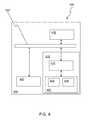
- FIG. 4is a schematic diagram illustrating an exemplary embodiment of a computing system 400 including a memory device 410 .
- a computing device 404may be representative of any device, appliance, or machine that may be configurable to manage memory device 410 .
- Memory device 410may include a memory controller 415 and a memory 422 .
- computing device 404may include: one or more computing devices and/or platforms, such as, e.g., a desktop computer, a laptop computer, a workstation, a server device, or the like; one or more personal computing or communication devices or appliances, such as, e.g., a personal digital assistant, mobile communication device, or the like; a computing system and/or associated service provider capability, such as, e.g., a database or data storage service provider/system; and/or any combination thereof.
- computing devices and/or platformssuch as, e.g., a desktop computer, a laptop computer, a workstation, a server device, or the like
- personal computing or communication devices or appliancessuch as, e.g., a personal digital assistant, mobile communication device, or the like
- a computing system and/or associated service provider capabilitysuch as, e.g., a database or data storage service provider/system; and/or any combination thereof.
- computing device 404may include one or more processing units 420 operatively coupled to memory 422 through a bus 440 and a host or memory controller 415 .
- Processing unit 420is representative of one or more circuits configurable to perform at least a portion of a data computing procedure or process.
- processing unit 420may include one or more processors, controllers, microprocessors, microcontrollers, application specific integrated circuits, digital signal processors, programmable logic devices, field programmable gate arrays, and the like, or any combination thereof.
- Processing unit 420may communicate with memory controller 415 to process memory-related operations, such as read, write, and/or erase, as well as memory partition processes discussed above, for example.
- Processing unit 420may include an operating system adapted to communicate with memory controller 415 . Such an operating system may, for example, generate commands to be sent to memory controller 415 over bus 440 . Such commands may include read/write instructions, for example.
- Memory 422is representative of any data storage mechanism.
- Memory 422may include, for example, a DRAM 424 and/or a persistent memory 426 .
- memory 422may comprise a main memory that includes at least a portion of persistent memory, as described above.
- Memory 422may also comprise cache memory that may likewise include at least a portion of persistent memory. While illustrated in this example as being separate from processing unit 420 , it should be understood that all or part of DRAM 424 may be provided within or otherwise co-located/coupled with processing unit 420 .
- one or more portions of memory 422may store signals representative of data and/or information as expressed by a particular state of memory 422 .
- an electronic signal representative of data and/or informationmay be “stored” in a portion of memory 422 by affecting or changing the state of such portions of memory 422 to represent data and/or information as binary information (e.g., ones and zeros).
- binary informatione.g., ones and zeros.
- such a change of state of the portion of memory to store a signal representative of data and/or informationconstitutes a transformation of memory 422 to a different state or thing.
- system 400may comprise two or more processing units 420 and main memory having at least one interface to connect to such multiple processors having on-board cache (e.g., via bus 440 to processing units 420 ), wherein at least a portion of main memory may comprise persistent memory.
- System 400may further comprise a memory controller to retrieve information from such a persistent main memory to initialize the on-board cache.
- Such persistent memorymay comprise PCM, for example.
- Computing device 404may include, for example, an input/output 432 .
- Input/output 432is representative of one or more devices or features that may be configurable to accept or otherwise introduce human and/or machine inputs, and/or one or more devices or features that may be configurable to deliver or otherwise provide for human and/or machine outputs.
- input/output device 432may include an operatively configured display, speaker, keyboard, mouse, trackball, touch screen, data port, etc.
Landscapes
- Engineering & Computer Science (AREA)
- Theoretical Computer Science (AREA)
- Physics & Mathematics (AREA)
- General Engineering & Computer Science (AREA)
- General Physics & Mathematics (AREA)
- Memory System Of A Hierarchy Structure (AREA)
- Techniques For Improving Reliability Of Storages (AREA)
- Memory System (AREA)
Abstract
Description
Claims (16)
Priority Applications (2)
| Application Number | Priority Date | Filing Date | Title |
|---|---|---|---|
| US14/245,916US9075725B2 (en) | 2010-06-09 | 2014-04-04 | Persistent memory for processor main memory |
| US14/791,030US9384134B2 (en) | 2010-06-09 | 2015-07-02 | Persistent memory for processor main memory |
Applications Claiming Priority (2)
| Application Number | Priority Date | Filing Date | Title |
|---|---|---|---|
| US12/797,512US8694737B2 (en) | 2010-06-09 | 2010-06-09 | Persistent memory for processor main memory |
| US14/245,916US9075725B2 (en) | 2010-06-09 | 2014-04-04 | Persistent memory for processor main memory |
Related Parent Applications (1)
| Application Number | Title | Priority Date | Filing Date |
|---|---|---|---|
| US12/797,512ContinuationUS8694737B2 (en) | 2010-06-09 | 2010-06-09 | Persistent memory for processor main memory |
Related Child Applications (1)
| Application Number | Title | Priority Date | Filing Date |
|---|---|---|---|
| US14/791,030ContinuationUS9384134B2 (en) | 2010-06-09 | 2015-07-02 | Persistent memory for processor main memory |
Publications (2)
| Publication Number | Publication Date |
|---|---|
| US20140223103A1 US20140223103A1 (en) | 2014-08-07 |
| US9075725B2true US9075725B2 (en) | 2015-07-07 |
Family
ID=45020213
Family Applications (3)
| Application Number | Title | Priority Date | Filing Date |
|---|---|---|---|
| US12/797,512Active2031-04-09US8694737B2 (en) | 2010-06-09 | 2010-06-09 | Persistent memory for processor main memory |
| US14/245,916ActiveUS9075725B2 (en) | 2010-06-09 | 2014-04-04 | Persistent memory for processor main memory |
| US14/791,030ActiveUS9384134B2 (en) | 2010-06-09 | 2015-07-02 | Persistent memory for processor main memory |
Family Applications Before (1)
| Application Number | Title | Priority Date | Filing Date |
|---|---|---|---|
| US12/797,512Active2031-04-09US8694737B2 (en) | 2010-06-09 | 2010-06-09 | Persistent memory for processor main memory |
Family Applications After (1)
| Application Number | Title | Priority Date | Filing Date |
|---|---|---|---|
| US14/791,030ActiveUS9384134B2 (en) | 2010-06-09 | 2015-07-02 | Persistent memory for processor main memory |
Country Status (6)
| Country | Link |
|---|---|
| US (3) | US8694737B2 (en) |
| JP (1) | JP5752989B2 (en) |
| KR (1) | KR101359813B1 (en) |
| CN (1) | CN102331974B (en) |
| DE (1) | DE102011076894B9 (en) |
| TW (1) | TWI506435B (en) |
Families Citing this family (22)
| Publication number | Priority date | Publication date | Assignee | Title |
|---|---|---|---|---|
| US8626997B2 (en) | 2009-07-16 | 2014-01-07 | Micron Technology, Inc. | Phase change memory in a dual inline memory module |
| US9448938B2 (en) | 2010-06-09 | 2016-09-20 | Micron Technology, Inc. | Cache coherence protocol for persistent memories |
| US8694737B2 (en) | 2010-06-09 | 2014-04-08 | Micron Technology, Inc. | Persistent memory for processor main memory |
| US8613074B2 (en) | 2010-09-30 | 2013-12-17 | Micron Technology, Inc. | Security protection for memory content of processor main memory |
| US9507534B2 (en)* | 2011-12-30 | 2016-11-29 | Intel Corporation | Home agent multi-level NVM memory architecture |
| CN103838746B (en)* | 2012-11-21 | 2017-05-31 | 杭州海康威视数字技术股份有限公司 | The method and the system of the shared data storage of multi-CPU system |
| CN103838676B (en)* | 2012-11-22 | 2017-10-17 | 华为技术有限公司 | Data-storage system, date storage method and PCM bridges |
| US20140181427A1 (en)* | 2012-12-21 | 2014-06-26 | Advanced Micro Devices, Inc. | Compound Memory Operations in a Logic Layer of a Stacked Memory |
| US9195614B2 (en) | 2013-01-08 | 2015-11-24 | International Business Machines Corporation | Instantaneous save/restore of virtual machines with persistent memory |
| US9367472B2 (en)* | 2013-06-10 | 2016-06-14 | Oracle International Corporation | Observation of data in persistent memory |
| EP3014448A4 (en)* | 2013-06-28 | 2017-03-08 | Hewlett-Packard Enterprise Development LP | Fault tolerance for persistent main memory |
| KR101635665B1 (en)* | 2013-10-31 | 2016-07-01 | 주식회사 엘지화학 | Apparatus and method that controls the data of application modules |
| WO2015147879A1 (en) | 2014-03-28 | 2015-10-01 | Hewlett-Packard Development Company, L.P. | Allowing use of a test key for a bios installation |
| US10922228B1 (en) | 2015-03-31 | 2021-02-16 | EMC IP Holding Company LLC | Multiple location index |
| US10210087B1 (en) | 2015-03-31 | 2019-02-19 | EMC IP Holding Company LLC | Reducing index operations in a cache |
| US10007435B2 (en)* | 2015-05-21 | 2018-06-26 | Micron Technology, Inc. | Translation lookaside buffer in memory |
| US20170123796A1 (en)* | 2015-10-29 | 2017-05-04 | Intel Corporation | Instruction and logic to prefetch information from a persistent memory |
| US10248571B2 (en)* | 2016-08-11 | 2019-04-02 | Hewlett Packard Enterprise Development Lp | Saving position of a wear level rotation |
| US11216396B2 (en) | 2016-09-29 | 2022-01-04 | Intel Corporation | Persistent memory write semantics on PCIe with existing TLP definition |
| US20190042445A1 (en)* | 2017-08-07 | 2019-02-07 | Intel Corporation | Technologies for caching persistent two-level memory data |
| CN108334331B (en)* | 2018-02-08 | 2021-05-25 | 苏州妙益科技股份有限公司 | Safe electric vehicle battery management system software upgrading method |
| US11544197B2 (en) | 2020-09-18 | 2023-01-03 | Alibaba Group Holding Limited | Random-access performance for persistent memory |
Citations (33)
| Publication number | Priority date | Publication date | Assignee | Title |
|---|---|---|---|---|
| JPH0358163A (en) | 1989-07-26 | 1991-03-13 | Nec Corp | Loosely coupled multiprocessor system |
| JPH06150031A (en) | 1992-10-30 | 1994-05-31 | Nec Corp | Cpu module |
| JPH0816470A (en) | 1994-07-04 | 1996-01-19 | Hitachi Ltd | Parallel computer |
| JPH0895861A (en) | 1994-09-22 | 1996-04-12 | Toshiba Corp | Computer with cache memory |
| JPH10161930A (en) | 1996-11-29 | 1998-06-19 | Hitachi Ltd | Multiprocessor system and cache coherency control method |
| US6003142A (en)* | 1996-12-10 | 1999-12-14 | Kabushiki Kaisha Toshiba | Test facilitating circuit of microprocessor |
| WO2001050269A2 (en) | 1999-12-30 | 2001-07-12 | Intel Corporation | A method and apparatus to perform a round robin and locking cache replacement scheme |
| US20030005237A1 (en)* | 2001-06-29 | 2003-01-02 | International Business Machines Corp. | Symmetric multiprocessor coherence mechanism |
| US6658539B2 (en) | 2001-10-16 | 2003-12-02 | International Business Machines Corporation | Super-coherent data mechanisms for shared caches in a multiprocessing system |
| CN1504902A (en) | 2002-12-05 | 2004-06-16 | 国际商业机器公司 | Method and system for keeping the consistency of data between storage blocks |
| JP2004521434A (en) | 2001-01-31 | 2004-07-15 | モトローラ・インコーポレイテッド | Non-volatile magnetic cache memory |
| JP2004334996A (en) | 2003-05-09 | 2004-11-25 | Hitachi Ltd | Semiconductor device |
| US20050160229A1 (en)* | 2004-01-16 | 2005-07-21 | International Business Machines Corporation | Method and apparatus for preloading translation buffers |
| US20050166020A1 (en)* | 2002-01-24 | 2005-07-28 | Intel Corporation | Methods and apparatus for cache intervention |
| TW200622905A (en) | 2004-08-26 | 2006-07-01 | Ibm | System and method for message delivery across a plurality of processors |
| WO2006107095A1 (en) | 2005-03-31 | 2006-10-12 | Nec Corporation | Computer system, memory management method, and program thereof |
| CN1864140A (en) | 2003-10-08 | 2006-11-15 | 艾利森电话股份有限公司 | Memory interface for systems with multiple processors and a memory system |
| JP2006323739A (en) | 2005-05-20 | 2006-11-30 | Renesas Technology Corp | Memory module, memory system and information apparatus |
| TW200710722A (en) | 2005-06-07 | 2007-03-16 | Advanced Micro Devices Inc | Microprocessor including a configurable translation lookaside buffer |
| WO2007105256A1 (en) | 2006-02-24 | 2007-09-20 | Fujitsu Limited | Multiprocessor system, processor, and cache control method |
| US20070226795A1 (en) | 2006-02-09 | 2007-09-27 | Texas Instruments Incorporated | Virtual cores and hardware-supported hypervisor integrated circuits, systems, methods and processes of manufacture |
| CN101131624A (en) | 2007-08-17 | 2008-02-27 | 杭州华三通信技术有限公司 | Storage control system and process node thereof |
| US20080082766A1 (en) | 2006-09-28 | 2008-04-03 | Okin Kenneth A | Systems and apparatus with programmable memory control for heterogeneous main memory |
| US20090037666A1 (en) | 2007-08-02 | 2009-02-05 | Freescale Semiconductor, Inc. | Cache locking device and methods thereof |
| JP2009295156A (en) | 2008-05-30 | 2009-12-17 | Intel Corp | Removal of invalidation transaction from snoop filter |
| US20100058046A1 (en)* | 2008-08-26 | 2010-03-04 | Texas Digital And Multimedia Systems | Method and Apparatus for Secure Instantly-Available Applications in a Computer System |
| US20100064111A1 (en)* | 2008-09-09 | 2010-03-11 | Kabushiki Kaisha Toshiba | Information processing device including memory management device managing access from processor to memory and memory management method |
| TW201017421A (en) | 2008-09-24 | 2010-05-01 | Panasonic Corp | Cache memory, memory system and control method therefor |
| TW201017408A (en) | 2008-07-07 | 2010-05-01 | Ibm | Efficient processing of data requests with the aid of a Region Cache |
| US20100211742A1 (en)* | 2009-02-13 | 2010-08-19 | Sebastian Turullols | Conveying critical data in a multiprocessor system |
| US20100293317A1 (en)* | 2009-05-14 | 2010-11-18 | Emanuele Confalonieri | Pcm memories for storage bus interfaces |
| US20110093646A1 (en) | 2009-10-16 | 2011-04-21 | Sun Microsystems, Inc. | Processor-bus attached flash main-memory module |
| US8180981B2 (en) | 2009-05-15 | 2012-05-15 | Oracle America, Inc. | Cache coherent support for flash in a memory hierarchy |
Family Cites Families (8)
| Publication number | Priority date | Publication date | Assignee | Title |
|---|---|---|---|---|
| US5442704A (en) | 1994-01-14 | 1995-08-15 | Bull Nh Information Systems Inc. | Secure memory card with programmed controlled security access control |
| EP1407456A2 (en) | 2001-07-18 | 2004-04-14 | Matsushita Electric Industrial Co., Ltd. | Writing apparatus, semiconductor memory card, writing proguram, and writing method |
| US7322042B2 (en) | 2003-02-07 | 2008-01-22 | Broadon Communications Corp. | Secure and backward-compatible processor and secure software execution thereon |
| US7644287B2 (en) | 2004-07-29 | 2010-01-05 | Microsoft Corporation | Portion-level in-memory module authentication |
| US7451166B2 (en) | 2005-01-13 | 2008-11-11 | International Business Machines Corporation | System and method for maintaining checkpoints of a keyed data structure using a sequential log |
| US20060265544A1 (en) | 2005-05-17 | 2006-11-23 | John Rudelic | Internally authenticated flash remediation |
| US8694737B2 (en) | 2010-06-09 | 2014-04-08 | Micron Technology, Inc. | Persistent memory for processor main memory |
| US9448938B2 (en) | 2010-06-09 | 2016-09-20 | Micron Technology, Inc. | Cache coherence protocol for persistent memories |
- 2010
- 2010-06-09USUS12/797,512patent/US8694737B2/enactiveActive
- 2011
- 2011-05-17JPJP2011110233Apatent/JP5752989B2/enactiveActive
- 2011-06-01DEDE102011076894.7Apatent/DE102011076894B9/enactiveActive
- 2011-06-08KRKR1020110054932Apatent/KR101359813B1/enactiveActive
- 2011-06-09CNCN201110159792.3Apatent/CN102331974B/enactiveActive
- 2011-06-09TWTW100120246Apatent/TWI506435B/enactive
- 2014
- 2014-04-04USUS14/245,916patent/US9075725B2/enactiveActive
- 2015
- 2015-07-02USUS14/791,030patent/US9384134B2/enactiveActive
Patent Citations (41)
| Publication number | Priority date | Publication date | Assignee | Title |
|---|---|---|---|---|
| JPH0358163A (en) | 1989-07-26 | 1991-03-13 | Nec Corp | Loosely coupled multiprocessor system |
| JPH06150031A (en) | 1992-10-30 | 1994-05-31 | Nec Corp | Cpu module |
| JPH0816470A (en) | 1994-07-04 | 1996-01-19 | Hitachi Ltd | Parallel computer |
| US5778429A (en) | 1994-07-04 | 1998-07-07 | Hitachi, Ltd. | Parallel processor system including a cache memory subsystem that has independently addressable local and remote data areas |
| JPH0895861A (en) | 1994-09-22 | 1996-04-12 | Toshiba Corp | Computer with cache memory |
| JPH10161930A (en) | 1996-11-29 | 1998-06-19 | Hitachi Ltd | Multiprocessor system and cache coherency control method |
| US6003142A (en)* | 1996-12-10 | 1999-12-14 | Kabushiki Kaisha Toshiba | Test facilitating circuit of microprocessor |
| WO2001050269A2 (en) | 1999-12-30 | 2001-07-12 | Intel Corporation | A method and apparatus to perform a round robin and locking cache replacement scheme |
| KR20020097145A (en) | 1999-12-30 | 2002-12-31 | 인텔 코오퍼레이션 | A method and apparatus to perform a round robin and locking cache replacement scheme |
| JP2004521434A (en) | 2001-01-31 | 2004-07-15 | モトローラ・インコーポレイテッド | Non-volatile magnetic cache memory |
| US20030005237A1 (en)* | 2001-06-29 | 2003-01-02 | International Business Machines Corp. | Symmetric multiprocessor coherence mechanism |
| US6658539B2 (en) | 2001-10-16 | 2003-12-02 | International Business Machines Corporation | Super-coherent data mechanisms for shared caches in a multiprocessing system |
| US20050166020A1 (en)* | 2002-01-24 | 2005-07-28 | Intel Corporation | Methods and apparatus for cache intervention |
| CN1504902A (en) | 2002-12-05 | 2004-06-16 | 国际商业机器公司 | Method and system for keeping the consistency of data between storage blocks |
| JP2004334996A (en) | 2003-05-09 | 2004-11-25 | Hitachi Ltd | Semiconductor device |
| CN1864140A (en) | 2003-10-08 | 2006-11-15 | 艾利森电话股份有限公司 | Memory interface for systems with multiple processors and a memory system |
| US20050160229A1 (en)* | 2004-01-16 | 2005-07-21 | International Business Machines Corporation | Method and apparatus for preloading translation buffers |
| US20070113044A1 (en)* | 2004-01-16 | 2007-05-17 | Day Michael N | Method and Apparatus for Preloading Translation Buffers |
| TW200622905A (en) | 2004-08-26 | 2006-07-01 | Ibm | System and method for message delivery across a plurality of processors |
| WO2006107095A1 (en) | 2005-03-31 | 2006-10-12 | Nec Corporation | Computer system, memory management method, and program thereof |
| US20090158000A1 (en) | 2005-03-31 | 2009-06-18 | Nec Corporation | Computer System, Memory Management Method and Program Thereof |
| JP2006323739A (en) | 2005-05-20 | 2006-11-30 | Renesas Technology Corp | Memory module, memory system and information apparatus |
| TW200710722A (en) | 2005-06-07 | 2007-03-16 | Advanced Micro Devices Inc | Microprocessor including a configurable translation lookaside buffer |
| US20070226795A1 (en) | 2006-02-09 | 2007-09-27 | Texas Instruments Incorporated | Virtual cores and hardware-supported hypervisor integrated circuits, systems, methods and processes of manufacture |
| WO2007105256A1 (en) | 2006-02-24 | 2007-09-20 | Fujitsu Limited | Multiprocessor system, processor, and cache control method |
| US20080320224A1 (en) | 2006-02-24 | 2008-12-25 | Fujitsu Limited | Multiprocessor system, processor, and cache control method |
| US20080082766A1 (en) | 2006-09-28 | 2008-04-03 | Okin Kenneth A | Systems and apparatus with programmable memory control for heterogeneous main memory |
| KR20100053540A (en) | 2007-08-02 | 2010-05-20 | 프리스케일 세미컨덕터, 인크. | Cache locking device and methods thereof |
| US20090037666A1 (en) | 2007-08-02 | 2009-02-05 | Freescale Semiconductor, Inc. | Cache locking device and methods thereof |
| WO2009017890A2 (en) | 2007-08-02 | 2009-02-05 | Freescale Semiconductor Inc. | Cache locking device and methods thereof |
| CN101131624A (en) | 2007-08-17 | 2008-02-27 | 杭州华三通信技术有限公司 | Storage control system and process node thereof |
| JP2009295156A (en) | 2008-05-30 | 2009-12-17 | Intel Corp | Removal of invalidation transaction from snoop filter |
| TW201017408A (en) | 2008-07-07 | 2010-05-01 | Ibm | Efficient processing of data requests with the aid of a Region Cache |
| US8055847B2 (en) | 2008-07-07 | 2011-11-08 | International Business Machines Corporation | Efficient processing of data requests with the aid of a region cache |
| US20100058046A1 (en)* | 2008-08-26 | 2010-03-04 | Texas Digital And Multimedia Systems | Method and Apparatus for Secure Instantly-Available Applications in a Computer System |
| US20100064111A1 (en)* | 2008-09-09 | 2010-03-11 | Kabushiki Kaisha Toshiba | Information processing device including memory management device managing access from processor to memory and memory management method |
| TW201017421A (en) | 2008-09-24 | 2010-05-01 | Panasonic Corp | Cache memory, memory system and control method therefor |
| US20100211742A1 (en)* | 2009-02-13 | 2010-08-19 | Sebastian Turullols | Conveying critical data in a multiprocessor system |
| US20100293317A1 (en)* | 2009-05-14 | 2010-11-18 | Emanuele Confalonieri | Pcm memories for storage bus interfaces |
| US8180981B2 (en) | 2009-05-15 | 2012-05-15 | Oracle America, Inc. | Cache coherent support for flash in a memory hierarchy |
| US20110093646A1 (en) | 2009-10-16 | 2011-04-21 | Sun Microsystems, Inc. | Processor-bus attached flash main-memory module |
Non-Patent Citations (16)
| Title |
|---|
| Chinese Office Action dated May 23, 2014 in corresponding Chinese Appl. No. 201110159792.3, filed Jun. 9, 2011, 4 pages. |
| Chinese Office Action dated Sep. 29, 2013 in corresponding Chinese Appl. No. 201110159792.3, filed Jun. 9, 2011, 13 pages. |
| Desikan, R., "On-chip MRAM as High-Bandwidth, Low-Latency Replacement for DRAM Physical Memories," Nov. 27, 2002, Department of Computer Sciences, University of Texas Austin. |
| Desikan, Rajagopalan, On-chip MRAM as high-bandwidth low latency replacement for DRAM physical memories, Nov. 27, 2002, Department of Computer Science, University of Texas at Austin.* |
| German Office Action dated Mar. 27, 2013 in corresponding German Appl. No. 102011076894.7, filed Jun. 1, 2011, 7 pages. |
| Intel Corp, "An introduction to the Intel QuickPath Interconnect" Jan. 2009, pp. 1-22, Document No. 320412-001US, Intel Corporation. |
| Japanese Decision of Rejection dated Dec. 24, 2013 in corresponding Japanese Appl. No. 2011-110233, filed May 17, 2011, 4 pages. |
| Japanese Notice of Rejection Grounds dated May 21, 2013 in corresponding Japanese Appl. No. 2011-110233, filed May 17, 2011, 5 pages. |
| Japanese Pre-Appeal Reexamination Report dated Jun. 20, 2014 in corresponding Japanese Appl. No. 2011-110233, filed May 17, 2011, 5 pages. |
| Korean Preliminary Rejection dated Apr. 15, 2013 in corresponding Korean Appl. No. 10-2011-54932, filed Jun. 8, 2011, 7 pages. |
| Lee, B.C. et al., "Phase-Change Technology and the Future of Main Memory," IEEE Computer Society, Jan./Feb. 2010, pp. 131-141. |
| Patterson, D.A. et al.: Computer Architecture a Quantitative Approach, 2nd Ed., Morgan Kaufmann Publishers, Inc. 1996, p. 654-693. |
| Sinharoy, B. et al., "Powers System Microarchitecture," IBM Journal of Research and Development-Power 5 and packing. vol. 49, Jul. 2005, p. 505-521. |
| Taiwan Office Action dated Dec. 27, 2014 in corresponding Taiwan Appl. No. 100120246, Filed Jun. 9, 2010, 15 pages. |
| U.S. Appl. No. 12/797,522, filed Jun. 9, 2010. |
| Wu, X. et al., "Hybrid Cache Architecture with Disparate Memory Technologies," ISCA 2009 Proceedings of the 36th Annual International Symposium on Computer Architecture, p. 34-45. |
Also Published As
| Publication number | Publication date |
|---|---|
| US20110307665A1 (en) | 2011-12-15 |
| CN102331974A (en) | 2012-01-25 |
| JP2011258189A (en) | 2011-12-22 |
| KR20110134840A (en) | 2011-12-15 |
| DE102011076894B4 (en) | 2018-05-24 |
| DE102011076894A1 (en) | 2011-12-15 |
| US20150309931A1 (en) | 2015-10-29 |
| CN102331974B (en) | 2015-01-28 |
| TW201227300A (en) | 2012-07-01 |
| KR101359813B1 (en) | 2014-02-07 |
| US8694737B2 (en) | 2014-04-08 |
| US9384134B2 (en) | 2016-07-05 |
| TWI506435B (en) | 2015-11-01 |
| US20140223103A1 (en) | 2014-08-07 |
| JP5752989B2 (en) | 2015-07-22 |
| DE102011076894B9 (en) | 2018-12-20 |
Similar Documents
| Publication | Publication Date | Title |
|---|---|---|
| US9384134B2 (en) | Persistent memory for processor main memory | |
| US9448938B2 (en) | Cache coherence protocol for persistent memories | |
| CN107408079B (en) | Memory controller with coherent unit for multi-level system memory | |
| US10019377B2 (en) | Managing cache coherence using information in a page table | |
| US20120102273A1 (en) | Memory agent to access memory blade as part of the cache coherency domain | |
| US20180032429A1 (en) | Techniques to allocate regions of a multi-level, multi-technology system memory to appropriate memory access initiators | |
| US12204478B2 (en) | Techniques for near data acceleration for a multi-core architecture | |
| US20170177482A1 (en) | Computing system having multi-level system memory capable of operating in a single level system memory mode | |
| EP3757800B1 (en) | Memory system, computing system, and methods thereof | |
| US20180088853A1 (en) | Multi-Level System Memory Having Near Memory Space Capable Of Behaving As Near Memory Cache or Fast Addressable System Memory Depending On System State | |
| US10210093B2 (en) | Memory device supporting both cache mode and memory mode, and operating method of the same | |
| US20180095884A1 (en) | Mass storage cache in non volatile level of multi-level system memory | |
| US7039763B2 (en) | Apparatus and method to share a cache memory | |
| US10949356B2 (en) | Fast page fault handling process implemented on persistent memory | |
| US20190042415A1 (en) | Storage model for a computer system having persistent system memory | |
| CN113448882A (en) | Apparatus and method for efficient management of multi-level memory | |
| US20110055482A1 (en) | Shared cache reservation | |
| US12019545B2 (en) | Memory system and operating method thereof | |
| Prasad et al. | Monarch: a durable polymorphic memory for data intensive applications | |
| US11526448B2 (en) | Direct mapped caching scheme for a memory side cache that exhibits associativity in response to blocking from pinning | |
| US20220229552A1 (en) | Computer system including main memory device having heterogeneous memories, and data management method thereof | |
| Mittal et al. | Cache performance improvement using software-based approach | |
| JP2024541672A (en) | Method for storing data operands in a memory unit and method for accessing data operands in a memory unit - Patents.com |
Legal Events
| Date | Code | Title | Description |
|---|---|---|---|
| FEPP | Fee payment procedure | Free format text:PAYOR NUMBER ASSIGNED (ORIGINAL EVENT CODE: ASPN); ENTITY STATUS OF PATENT OWNER: LARGE ENTITY | |
| STCF | Information on status: patent grant | Free format text:PATENTED CASE | |
| AS | Assignment | Owner name:U.S. BANK NATIONAL ASSOCIATION, AS COLLATERAL AGENT, CALIFORNIA Free format text:SECURITY INTEREST;ASSIGNOR:MICRON TECHNOLOGY, INC.;REEL/FRAME:038669/0001 Effective date:20160426 Owner name:U.S. BANK NATIONAL ASSOCIATION, AS COLLATERAL AGEN Free format text:SECURITY INTEREST;ASSIGNOR:MICRON TECHNOLOGY, INC.;REEL/FRAME:038669/0001 Effective date:20160426 | |
| AS | Assignment | Owner name:MORGAN STANLEY SENIOR FUNDING, INC., AS COLLATERAL AGENT, MARYLAND Free format text:PATENT SECURITY AGREEMENT;ASSIGNOR:MICRON TECHNOLOGY, INC.;REEL/FRAME:038954/0001 Effective date:20160426 Owner name:MORGAN STANLEY SENIOR FUNDING, INC., AS COLLATERAL Free format text:PATENT SECURITY AGREEMENT;ASSIGNOR:MICRON TECHNOLOGY, INC.;REEL/FRAME:038954/0001 Effective date:20160426 | |
| AS | Assignment | Owner name:U.S. BANK NATIONAL ASSOCIATION, AS COLLATERAL AGENT, CALIFORNIA Free format text:CORRECTIVE ASSIGNMENT TO CORRECT THE REPLACE ERRONEOUSLY FILED PATENT #7358718 WITH THE CORRECT PATENT #7358178 PREVIOUSLY RECORDED ON REEL 038669 FRAME 0001. ASSIGNOR(S) HEREBY CONFIRMS THE SECURITY INTEREST;ASSIGNOR:MICRON TECHNOLOGY, INC.;REEL/FRAME:043079/0001 Effective date:20160426 Owner name:U.S. BANK NATIONAL ASSOCIATION, AS COLLATERAL AGEN Free format text:CORRECTIVE ASSIGNMENT TO CORRECT THE REPLACE ERRONEOUSLY FILED PATENT #7358718 WITH THE CORRECT PATENT #7358178 PREVIOUSLY RECORDED ON REEL 038669 FRAME 0001. ASSIGNOR(S) HEREBY CONFIRMS THE SECURITY INTEREST;ASSIGNOR:MICRON TECHNOLOGY, INC.;REEL/FRAME:043079/0001 Effective date:20160426 | |
| AS | Assignment | Owner name:JPMORGAN CHASE BANK, N.A., AS COLLATERAL AGENT, ILLINOIS Free format text:SECURITY INTEREST;ASSIGNORS:MICRON TECHNOLOGY, INC.;MICRON SEMICONDUCTOR PRODUCTS, INC.;REEL/FRAME:047540/0001 Effective date:20180703 Owner name:JPMORGAN CHASE BANK, N.A., AS COLLATERAL AGENT, IL Free format text:SECURITY INTEREST;ASSIGNORS:MICRON TECHNOLOGY, INC.;MICRON SEMICONDUCTOR PRODUCTS, INC.;REEL/FRAME:047540/0001 Effective date:20180703 | |
| AS | Assignment | Owner name:MICRON TECHNOLOGY, INC., IDAHO Free format text:RELEASE BY SECURED PARTY;ASSIGNOR:U.S. BANK NATIONAL ASSOCIATION, AS COLLATERAL AGENT;REEL/FRAME:047243/0001 Effective date:20180629 | |
| MAFP | Maintenance fee payment | Free format text:PAYMENT OF MAINTENANCE FEE, 4TH YEAR, LARGE ENTITY (ORIGINAL EVENT CODE: M1551); ENTITY STATUS OF PATENT OWNER: LARGE ENTITY Year of fee payment:4 | |
| AS | Assignment | Owner name:MICRON TECHNOLOGY, INC., IDAHO Free format text:RELEASE BY SECURED PARTY;ASSIGNOR:MORGAN STANLEY SENIOR FUNDING, INC., AS COLLATERAL AGENT;REEL/FRAME:050937/0001 Effective date:20190731 | |
| AS | Assignment | Owner name:MICRON TECHNOLOGY, INC., IDAHO Free format text:RELEASE BY SECURED PARTY;ASSIGNOR:JPMORGAN CHASE BANK, N.A., AS COLLATERAL AGENT;REEL/FRAME:051028/0001 Effective date:20190731 Owner name:MICRON SEMICONDUCTOR PRODUCTS, INC., IDAHO Free format text:RELEASE BY SECURED PARTY;ASSIGNOR:JPMORGAN CHASE BANK, N.A., AS COLLATERAL AGENT;REEL/FRAME:051028/0001 Effective date:20190731 | |
| MAFP | Maintenance fee payment | Free format text:PAYMENT OF MAINTENANCE FEE, 8TH YEAR, LARGE ENTITY (ORIGINAL EVENT CODE: M1552); ENTITY STATUS OF PATENT OWNER: LARGE ENTITY Year of fee payment:8 |