US9071243B2 - Single ended configurable multi-mode driver - Google Patents
Single ended configurable multi-mode driverDownload PDFInfo
- Publication number
- US9071243B2 US9071243B2US13/174,630US201113174630AUS9071243B2US 9071243 B2US9071243 B2US 9071243B2US 201113174630 AUS201113174630 AUS 201113174630AUS 9071243 B2US9071243 B2US 9071243B2
- Authority
- US
- United States
- Prior art keywords
- driver
- voltage
- voltage swing
- termination resistance
- signal
- Prior art date
- Legal status (The legal status is an assumption and is not a legal conclusion. Google has not performed a legal analysis and makes no representation as to the accuracy of the status listed.)
- Active
Links
Images


Classifications
- H—ELECTRICITY
- H03—ELECTRONIC CIRCUITRY
- H03K—PULSE TECHNIQUE
- H03K19/00—Logic circuits, i.e. having at least two inputs acting on one output; Inverting circuits
- H03K19/0005—Modifications of input or output impedance
- H—ELECTRICITY
- H03—ELECTRONIC CIRCUITRY
- H03K—PULSE TECHNIQUE
- H03K19/00—Logic circuits, i.e. having at least two inputs acting on one output; Inverting circuits
- H03K19/0175—Coupling arrangements; Interface arrangements
- H03K19/0185—Coupling arrangements; Interface arrangements using field effect transistors only
- H03K19/018557—Coupling arrangements; Impedance matching circuits
- H03K19/018571—Coupling arrangements; Impedance matching circuits of complementary type, e.g. CMOS
- H—ELECTRICITY
- H03—ELECTRONIC CIRCUITRY
- H03K—PULSE TECHNIQUE
- H03K3/00—Circuits for generating electric pulses; Monostable, bistable or multistable circuits
- H03K3/01—Details
- H03K3/012—Modifications of generator to improve response time or to decrease power consumption
- H—ELECTRICITY
- H04—ELECTRIC COMMUNICATION TECHNIQUE
- H04L—TRANSMISSION OF DIGITAL INFORMATION, e.g. TELEGRAPHIC COMMUNICATION
- H04L12/00—Data switching networks
- H04L12/02—Details
- H04L12/12—Arrangements for remote connection or disconnection of substations or of equipment thereof
- H—ELECTRICITY
- H04—ELECTRIC COMMUNICATION TECHNIQUE
- H04L—TRANSMISSION OF DIGITAL INFORMATION, e.g. TELEGRAPHIC COMMUNICATION
- H04L25/00—Baseband systems
- H04L25/02—Details ; arrangements for supplying electrical power along data transmission lines
- H04L25/0264—Arrangements for coupling to transmission lines
- H04L25/0278—Arrangements for impedance matching
- H—ELECTRICITY
- H04—ELECTRIC COMMUNICATION TECHNIQUE
- H04L—TRANSMISSION OF DIGITAL INFORMATION, e.g. TELEGRAPHIC COMMUNICATION
- H04L25/00—Baseband systems
- H04L25/02—Details ; arrangements for supplying electrical power along data transmission lines
- H04L25/0264—Arrangements for coupling to transmission lines
- H04L25/028—Arrangements specific to the transmitter end
Definitions
- Embodiments of the inventiongenerally relate to the field of electronic devices and, more particularly, to a single-ended configurable multi-mode driver.
- a driver circuit or apparatusIn the communication of signals between devices or elements, a driver circuit or apparatus is used to drive the signal.
- a drivermay be required for driving signal in a high-speed memory interface and similar processes.
- driver circuitsNumerous different conventional circuit technologies may be used for driver circuits.
- the technologiesmay in complexity and structure, including voltage-mode drivers with or without termination resistances, differential drivers, and current-mode drivers.
- FIG. 1illustrates an embodiment of elements of an I/O link
- FIG. 2illustrates a single-ended voltage-mode driver
- FIG. 3illustrates a single-ended voltage-mode driver with termination provided on transmitting and receiving sides
- FIG. 4is an illustration of elements of a driver system structure
- FIG. 5illustrates a voltage-mode differential driver
- FIG. 6illustrates a current-mode logic driver
- FIG. 7illustrates a single ended current-mode driver
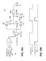
- FIG. 8Aillustrates an embodiment of a configurable single-ended driver structure
- FIG. 8Billustrates an embodiment of a configurable single-ended driver structure with current source
- FIG. 9illustrates an embodiment of a configurable single-ended voltage-mode driver
- FIG. 10is illustrates an embodiment of a configurable single-ended voltage-mode driver
- FIG. 11is an illustration of an embodiment of a configurable single-ended mixed mode driver
- FIG. 12illustrates an embodiment of a configurable single-ended mixed mode driver
- FIG. 13is an illustration of an embodiment of a feedback circuit to generate a bias voltage for a configurable driver
- FIG. 14Ais an illustration of an embodiment of an apparatus to derive a voltage swing for a bias voltage using a configurable driver circuit
- FIG. 14Bis an illustration of an embodiment of an apparatus to derive a voltage swing for a bias voltage using a replica of a configurable driver circuit
- FIG. 15illustrates an embodiment of an apparatus for impedance detection and adjustment for a configurable driver
- FIG. 16is an illustration of impedance characteristics of certain drivers
- FIG. 17is an illustration of speed versus power tradeoff for an embodiment of a driver
- FIG. 18Ais an illustration of an embodiment of a pulsing mechanism for a driver
- FIG. 18Bis an illustration of signals generated by an embodiment of a pulsing mechanism of a driver
- FIG. 19illustrates an embodiment of a driver apparatus for an interface between devices
- FIG. 20is a flowchart to illustrate an embodiment of a process for driving data signals from a first device to a second device.
- Embodiments of the inventionare generally directed to a single-ended configurable multi-mode driver.
- an embodiment of a single-ended driver apparatusincludes an input to receive an input signal, an output to transmit a driven signal generated from the input signal on a communication channel, a mechanism for independently configuring a termination resistance of the driver apparatus, and a mechanism for independently configuring a voltage swing of the driven signal without modifying a supply voltage for the apparatus.
- a systemin a second aspect of the invention, includes a communication channel; a single-ended driver apparatus coupled with the communication channel to provide a driven signal, the transmitting apparatus including an mechanism for independently configuring a termination resistance of the driver apparatus, and an mechanism for independently configuring a voltage swing of the driven signal without modifying a supply voltage for the driver apparatus; and a receiving apparatus coupled with the communication channel to receive the driven signal.
- an embodiment of a system for signal communicationincludes a first device including a first single-ended driver apparatus and first receiver apparatus and a second device coupled with the first device via a communication channel including a second single-ended driver apparatus and a second receiver apparatus.
- Termination resistances and voltage swings of the first driver apparatus and second driver apparatusare independently configurable, and the voltage swing and the termination resistance of the first driver apparatus of the first device may be configured to be different from the voltage swing and termination resistance of the second driver apparatus.
- a method for configuring a communication interfaceincludes determining parameters for an interface between a first device and a second device, the first device including a configurable driver apparatus and the second device including a receiving apparatus; independently configuring a termination resistance of the driver apparatus of the first device based on the determined parameters; and independently configuring a voltage swing of the driver apparatus of the first device based on the determined parameters without modifying a supply voltage for the first device.
- Embodiments of the inventionare generally directed to a single-ended configurable multi-mode driver.
- a method, apparatus, or systemprovides for a single-ended configurable multi-mode driver.
- an apparatus or systemprovides a driver to provide signaling, such as a driver for high-speed wire-line interfaces, including, for example, DRAM (dynamic random access memory) interfaces.
- a drivermay be configurable for voltage swing characteristics and termination resistances.
- a driveris a multi-mode mode, where “multi-mode” refers to operation at multiple different speeds.
- an apparatusincludes an input to receive an input signal, an output to transmit a driven signal generated from the input signal on a communication channel, a mechanism for configuring a termination resistance of the driver apparatus, and a mechanism for configuring a voltage swing of the driven signal.
- a systemin some embodiments, includes a communication channel, a driver apparatus coupled with the communication channel to provide a driven signal, the transmitting apparatus including a mechanism for configuring a termination resistance of the driver apparatus and a mechanism for configuring a voltage swing of the driven signal, and a receiving apparatus coupled with the communication channel to receive the driven signal.
- FIG. 1illustrates an embodiment of elements of an I/O link.
- parallel data 105is serialized by a serializer 110 , with the serialized output being received by a driver 130 for transmission via a channel 135 .
- the serializer 110 and driver 130may be clocked by a clock signal 125 produced by a phase lock loop (PLL) circuit 115 , which creates the clock signal 125 using a reference clock signal 120 .
- PLLphase lock loop
- the serialized data transmitted via the channel 135is received by a signal equalizer 140 , which provides equalized data signals to a clock and data recovery element 145 .
- the clock and data recovery elementprovides recovered data to a deserializer 155 and a recovered clock signal 150 to the equalizer 140 and deserializer 155 .
- the deserializer 155deserializes the data and produces a parallel data output 160 .
- the driver 130is a configurable multi-mode driver that may be configured to control power consumption.
- FIG. 2illustrates a single-ended voltage-mode driver.
- a single ended (as opposed to differential) driver 200may, for example, provide transmission for speeds up to 1 Gbps (gigabit per second).
- the driver 200operates to drive signals via a channel (CHAN) 270 to a receiver (RX) 250 , the channel connection of the driver 200 being coupled with ground by a first capacitor (C 1 ) 262 and the channel connection of the receiver 280 being coupled with ground by a second capacitor (C 2 ) 282 .
- the driver 200includes transistors M 11 210 , M 21 216 , M 12 220 , M 22 226 . . . M 1 N 230 , M 2 N 236 , which are used as switches, with variation in termination being provided with the switchable combination of resistors R 11 212 through R 2 N 234 as controlled by the transistors.
- driver 200over certain technologies is that the driver generally consumes only dynamic power.
- signal integrity performancemay deteriorate rapidly due to signal reflections and supply bounce, which thus limits speeds and BER (bit error rate). Therefore, at higher speeds two techniques are commonly used to combat signal reflections and supply bounce.
- a termination resistormay be used on both the receiver and transmitter ends.
- differential circuit structuresare used. However, both of these structures or methods have significant power penalties, which are described in more detail below.
- FIG. 3illustrates a single-ended voltage-mode driver with termination resistance provided on transmitting and receiving sides.
- a driver 300is coupled with a receiver (RX) 380 via a channel (CHAN) 370 , with the channel connection to driver 300 being coupled with ground by a first capacitor (C 1 ) 362 and the channel connection of the receiver 380 being coupled with ground by a second capacitor (C 2 ) 382 .
- Driver 300includes a first transistor (M 1 ) 310 operating as a switch between a voltage VDDQ and a first end of a first resistor (R 1 ) 312 , where a second end of R 2 314 is coupled with CHAN 370 .
- Driver 300further includes a second transistor (M 2 ) 316 operating as a switch between ground and a first end of a second resistor (R 2 ) 314 , wherein a second end of R 2 314 is coupled with a second end of R 1 312 and CHAN 370 .
- M 2second transistor
- R 2resistor
- FIG. 4is an illustration of elements of a driver system structure.
- a low supply voltagemay be utilized to reduce power.
- this voltage supplyis generated from a switching regulator that is external to the chip.
- the supplyis Vs/2, which is not the standard V DD , and the swing is Vs/4. Therefore, the output swing will be dependent on an external supply.
- slew rate control 430is achieved by impedance control 420 involving the control of the PMOS (P-type metal-oxide-semiconductor) device resistance by adjusting a gate voltage V sr .
- Pre-emphasis 410is achieved by replicating the same unit driver and inputting past and present samples through each driver.
- the output resistance of the driveris controlled by having the predriver (PreDrvr) swing between zero and PVDD.
- PVDDis set based on the resistance of the NMOS (N-type metal-oxide-semiconductor) devices (dependent on V gs of the NMOS).
- the NMOS transistors in the final stageoperate only in the triode region (resistive region). In contrast, in some embodiments devices operate in both triode and current source modes, depending on the transistor.
- FIG. 5illustrates a voltage-mode differential driver. Differential structures may be used to mitigate supply bounce and common-mode noise.
- FIG. 5illustrates one possible voltage-mode differential driver implementation.
- a driver 500includes a first differential structure 510 and a second differential structure 520 .
- the first differential structure 510is coupled with a receiver (RX) 580 via a first channel (CHAN- 1 ) 570 and the second differential structure 520 is coupled with the receiver 580 via a second channel (CHAN- 2 ) 572 .
- the channel connection of each of the differential structuresis coupled with ground via a first capacitor (C 1 ) 562 and 564 , and each of two inputs to the receiver 580 is coupled with ground by a second capacitor (C 2 ) 582 and 584 .
- Each of the differential structuresincludes a first transistor (M 1 ) 510 or 520 as a switch between a voltage VDDQ and a first end of a first resistor (R 1 ) 512 or 522 , where a second end of the first resistor 512 or 522 is coupled with the channel 570 or 572 .
- Each of the differential structuresfurther includes a second transistor (M 2 ) 516 or 526 as a switch between ground and a first end of a second resistor (R 2 ) 514 or 524 , wherein a second end of the second resistor 514 or 524 is coupled with the channel 570 or 572 .
- the net current drawn from the supplyis constant, irrespective of the bit state, thus mitigating supply bounce.
- the driveris required to operate at double the speed of the single-ended structure to maintain the same per pin bandwidth efficiency.
- the channel requirementsmay pose undue constraints in many applications.
- the voltage swingsare not easily configured or programmed, and hence power dissipation is not easily adaptable with data speeds.
- FIG. 6illustrates a current-mode logic (CML) driver.
- a current source (I) 640is coupled with a first end of a first transistor (M 1 ) 610 and a second transistor (M 2 ) 620 , where a second end of the M 1 610 is coupled with a first channel (CHAN- 1 ) 670 and with a first end of a resistor (R) 612 , the second end of R 612 being coupled with ground, where a second end of M 2 620 is coupled with a second channel (CHAN- 2 ) 672 and with a first end of a resistor (R) 622 , the second end of R 622 being coupled with ground.
- a current source (I) 640is coupled with a first end of a first transistor (M 1 ) 610 and a second transistor (M 2 ) 620 , where a second end of the M 1 610 is coupled with a first channel (CHAN- 1 ) 670 and with a first end of a resistor (
- a first end of a receiver (RX) 680is coupled with CHAN- 1 670 and a first end of a termination resistor (2*Rt) 682 , and a second end of RX 680 is coupled with CHAN- 2 672 and a second end of the termination resistor 682 .
- Current-mode logic driverscan provide flexibility to modify swings with current, and thus such drivers are commonly used.
- a CML driversuch as driver 600 , draws a static current irrespective of the state of the output. For this reason, the CML driver is generally not suitable for applications where the data is transmitted in bursts.
- FIG. 7illustrates a single ended current-mode driver.
- a first end of a transistor (M 1 ) 710is coupled with a voltage source V DD and a second end of M 1 710 is coupled with a channel (CHAN) 770 and with a first end of a resistor (R) 712 , the second end of R 712 being coupled with ground.
- a first end of a receiver (RX) 780is coupled with CHAN 770 and a first end of a termination resistor (Rt) 782 , with a second end of Rt 782 being coupled with ground.
- a single-ended current-mode driversuch as driver 700 generally consumes twice as much current as a differential driver, such as driver 600 illustrated in FIG. 6 , for similar voltage swings, and thus has significant limitations.
- a driverincludes elements to allow for improvements in operation in comparison with conventional drivers.
- driverinclude elements to reduce power consumption and provide improved bandwidth efficiency per pin, thereby reducing the effective swing (or current) in the driver and providing more of available current in the driver to an attached load.
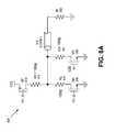
- FIG. 8Aillustrates an embodiment of a configurable single-ended driver structure.
- a driver 800(which may be referred to herein as a Type I driver) is coupled with a receiver apparatus including a termination resistance (Rt) 882 via a channel (CHAN) 870 .
- Driver 800includes a first transistor (M 1 ) acting as a switch between a voltage V DD and a first end of a first resistor (R 1 ) 812 , where a second end of R 1 812 is coupled with a transmitter side of CHAN 870 .
- Driver 800further includes a second transistor (M 2 ) 816 acting as a switch between ground and a first end of a second resistor (R 2 ) 814 , with a second end of R 2 814 being coupled with CHAN 870 .
- driverfurther includes a third transistor (M 3 ) 826 acting as a switch between ground and a first end of a third resistor (R 3 ) 824 , with a second end of R 3 824 being coupled with CHAN 870 .
- transistors M 1 810 and M 3 826operate as switches whereby a voltage division between the series connection of M 1 /R 1 and M 3 /R 3 may be utilized to set a voltage swing at the driver output.
- a voltage swingthat may be set independently of the supply (by adjusting the resistance values) the output voltage, and hence the power dissipation, may be minimized to suit a particular interface.
- the structure provided in FIG. 8Aoperates without requiring a bias voltage, and may be utilized in applications where startup time is critical.
- the driver 800may be used to provide an improved power dissipation efficiency compared to a single-ended current-mode driver.
- branches of the driver circuitalso referred to here as strings
- each of such stringsmay represent multiple parallel strings.
- programmability and configurability of the driver apparatus 800is provided by the multiple strings of transistors and resistors, where the driver 800 includes only those strings that provide the correct output impedance or current capability.
- the multiple stringsmay be utilized to track PVT (Process, Voltage, Temperature) variations in a system.
- PVTProcess, Voltage, Temperature
- M 1 810 and R 1 812represent the equivalent of numerous such strings.
- the number of strings selected for the driver 800depends on the configurability required for the driver.
- the driver 800may operate with large Vt (threshold voltage) transistors, thus making the structure of driver 800 suitable for DRAM-type processes.
- adjustments to R 1 and R 3may be made to satisfy required Z 0 , Vdriverout, and power dissipation simultaneously, thereby allowing the circuit structure to be adapted to various applications.
- FIG. 8Billustrates an embodiment of a configurable single-ended driver structure with current source.
- driver 801(which is another version of the type-I driver) further includes a configurable current source 820 (where current source transistor M 4 is the current source), where the current source is coupled with the transmitter side of CHAN 870 .
- the current source 820is illustrated as the current source transistor M 4 , where the mirroring element of the current source is not illustrated here.
- the current source 820may provide additional output current, if required.
- the current source 820 of driver 801is programmable in order to provide the current necessary.
- a high voltage for the driver 801may be achieved by switching on the first transistor 810 , second transistor 816 , and current source transistor 820 and switching off the third transistor 826 , where the high voltage value is defined by the ratio of R 1 812 and R 3 824 and the current from current source 820 .
- a low voltage for the driver 801may be achieved by switching off the first transistor 810 , the second transistor 814 , and the current source transistor 820 , and switching on the third transistor 826 .
- the value of the termination in the high voltage stateis set by the equivalent parallel resistance of R 1 and R 3 . while the termination in the low voltage state set by R 2 .
- the equivalent resistance of R 1 812 , R 2 814 and R 3 824may be derived from using multiple parallel strings of the units illustrated, as described above with regard to FIG. 8A , and thus R 1 , R 2 , and R 3 are effectively variable by enabling one or more of the parallel strings.
- the string of M 1 810 and R 1 812may be the equivalent of multiple parallel strings of resistances and transistors, where FIG. 8B provides an equivalent representation of the multiple strings. This is also true for the other strings illustrated, such as the string including M 2 816 and R 2 814 and the string including M 3 826 and R 3 824 .
- enablement of one or more of the multiple stringsmay be utilized to provide programmability for the termination resistance.
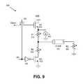
- FIG. 9illustrates an embodiment of a configurable single-ended voltage-mode driver.
- a driver 900(which may be referred to herein as a type-II driver) is a voltage-mode driver.
- a first transistor (M 1 ) 910 of the driver 900acts as a source follower coupled with a terminal of transistor 942 , where a second terminal of transistor 942 is coupled with a bias voltage Vbias 1 , and a second transistor (M 2 ) 916 acts as a switch, the gate of M 2 916 being coupled with inverter 944 , which receives voltage V in .
- a first terminal of M 1 910is coupled with voltage V DD and a second terminal of M 1 910 is coupled with a first end of a first variable resistor (R 1 ) 912 and a bleeder current source (Ib) 940 .
- a second end of R 1 912is coupled with a channel (CHAN) 970 and a first end of a second variable resistor (R 2 ) 914 .
- a second end of R 2 914is coupled with a first terminal of M 2 916 , with a second terminal of M 2 916 being coupled with ground.
- Coupled with a receiver end of CHAN 970is a third variable resistor (R 3 ) 982 representing a termination resistance.
- an input to M 1 910is biased to Vbias 1 when the output is high and pulled to ground in the OFF state.
- the output swing of the driver 900may be controlled to a minimum needed value, and hence the corresponding power dissipation may be reduced. For example, if a swing of 300 mV is needed at R 3 982 , then 6 mA of current is supplied by M 1 910 , which is half the current and resulting power consumption of typical single-ended solutions (for which the current would be 12 mA with 1.2 V V DD in this example).
- the output impedance of the driver 900is the sum of R 1 and the small/large signal impedance seen at the source of M 1 910 .
- the effect of variation in small/large signal impedancemay be mitigated by utilizing a large R 1 912 value relative to the source impedance of M 1 910 .
- the bleeder current source Ib 940provides additional flexibility in adjusting the bias points of M 1 .
- the Ib currentis a fraction of the overall current, and in zero state only M 2 and R 2 are conducting to ground and hence the driver 900 has essentially no static current.
- FIG. 10illustrates an embodiment of a configurable single-ended voltage-mode driver.
- FIG. 10illustrates a modified form of type-II voltage-mode driver 1000 .
- a first terminal of a first transistor (M 1 —receiving bias voltage Vbias 1 ) 1010is coupled with voltage V DD and a second terminal of M 1 1010 is coupled with a first end of a first variable resistor (R 1 ) 1012 and a bleeder current source (Ib) 1040 .
- a first terminal of a second transistor (M 2 —receiving input signal Vin) 1016is coupled with a first end of a second variable resistor (R 2 ) 1014 .
- a second end of R 1 1012is coupled with a first terminal of a third transistor (M 3 —receiving input signal Vin) 1042 , with a second terminal of M 3 1042 being coupled with a first end of a channel (CHAN) 1070 and a first second of R 2 1014 . Coupled with a second end of CHAN 1070 is a third variable resistor (R 3 ) 1082 .
- M 3third transistor
- R 3third variable resistor
- the switch M 3 1042is in series with M 1 1010 .
- the functionality of the illustrated Type-II drivermay include the functionality of a type-I driver.
- the structure illustrated in FIG. 10would also be suitable for drivers that do not include a termination resistance on the receiver side.
- the bleeder current source Ib 1040may be utilized to ensure that transistor M 1 1010 is always on with suitable overdrive voltage.
- a voltage swing and a termination resistance of the driver 1000are configurable by adjustment of resistance of the first variable resistor 1012 and the second variable resistor 1014 .
- the voltage swingis further defined by the bias voltage Vbias 1 .
- transistors M 3 1042 and M 2 1016operate in a complementary fashion. For example, when M 3 is on, M 2 is ideally off, and vice versa.
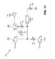
- FIG. 11is an illustration of an embodiment of a configurable single-ended mixed mode driver.
- a “type-III” mixed voltage-mode current-mode driveris provided.
- a driver 1100includes a first transistor (M 1 ) 1110 with a first terminal coupled with voltage V DD and a second terminal coupled with a first end of a first variable resistor (R 1 ) 1122 , a first end of a second variable resistor (R 2 ) 1114 , and a first transmitter end of a channel (CHAN) 1170 .
- a second end of R 2 1114is coupled with a first terminal of a second transistor (M 2 ) 1116 , with a second terminal of M 2 1116 being coupled with ground.
- a third transistor (M 3 ) 1120includes a first terminal coupled with V DD and a second terminal coupled with a second end of R 1 1122 and a bleeder current source (Ib) 1140 , with the gate of M 3 1120 being coupled with an inverter 1142 .
- M 1 1110acts as a switching current source during an ON state. Further, the input to M 3 is swing regulated by the inverter 1142 , whose supply voltage is regulated to a reference voltage (V REF ), thus controlling the voltage swing at the output of the driver 1100 . In some embodiments, M 1 1110 may be removed from the driver circuit if the M 3 leg provides adequate swing and termination control. In some embodiments, M 1 1110 may be utilized as a de-emphasis tap providing a required current during a transition to compensate for non-ideal channel effects.
- a number of tapsmay be extended by including an additional number of strings (such as M 1 1110 ) with appropriate de-emphasis taps (where such additional number of strings are not illustrated here).
- the illustrated structurecan be inverted such that the swings are not referenced to ground but with reference to V DD .
- FIG. 12illustrates an embodiment of a configurable single-ended mixed mode driver.
- the driver 1200includes a first transistor (M 1 ) 1211 (receiving bias voltage Vbias 1 ) with a first terminal coupled with a first end of a first variable resistor (R 1 ) 1212 .
- a second end of R 1 1212is coupled with a transmitter end of a channel (CHAN) 1270 and a first end of a second adjustable resistor (R 2 ) 1214 .
- a second end of R 2 1214is coupled with a first terminal of a second transistor (M 2 ) 1216 , where a second terminal of M 2 1216 is coupled with ground.
- a second terminal of M 1 1211is coupled with a first terminal of a third transistor (M 3 ) 1210 , a second terminal of M 3 1210 being coupled with voltage V DD .
- a fourth transistor (M 4 ) 1220(receiving bias voltage Vbias 2 ) includes a first terminal coupled with voltage V DD and a second terminal coupled with a first terminal of a fifth transistor (M 5 ) 1221 , where a second terminal of M 5 1221 is coupled with the first end of CHAN 1270 .
- a second end of CHAN 1270is coupled with an adjustable termination resistance (R 3 ) 1282 .
- M 4 1220operates as a current source
- M 1 1211operates as a source follower
- M 3 1210 and M 5 1221operate as switches.
- a driversuch as one of the drivers illustrated in FIGS. 8A through 12 , may provide the following benefits:
- Voltage swingsmay be configured or programmed to reduce power dissipation, based on system requirements.
- Termination resistancemay be configured or programmed based on system requirements.
- Voltage swingsmay be de-coupled from the value of the supply voltage.
- Driversmay be implemented with transistors that have large threshold voltages, especially in DRAM processes.
- driver circuits presented in FIGS. 8A through 12relate to:
- FIG. 13is an illustration of an embodiment of a feedback circuit to generate a bias voltage for a configurable driver.
- a bias voltage generator 1300provides for comparison of an actual driver voltage (Vdriverout) with a required voltage swing (Vswing) at the output to control the bias voltage.
- a generator circuit 1300includes an error/reference generator 1344 that receives Vdriveout and Vswing as comparison inputs.
- the error/reference generatorfurther receives an input of certain programmable bits that provide flexibility in controlling the reference generator output.
- the error voltage between Vdriveout and Vswingis provided to a digital-to-analog converter 1342 to generate a Vref value as a first input to a amplifier 1340 , where the output of the amplifier is coupled with a first terminal of capacitor C 1320 and to a gate of a transistor (M 8 ) 1310 , with a first terminal of M 8 being coupled with voltage V DD and a second terminal of M 8 1310 being coupled with an output node for bias input Vbias 1 for a driver, the node being further coupled with a second input of amplifier 1340 and to a first end of resistor Rbg 1314 , wherein a second end of Rbg is coupled with ground.
- a voltagemay be referenced to a source voltage V DD as well as being referenced to a ground potential.
- a method or apparatusmay be provided to derive a DC voltage swing of a driver for a particular bias voltage (Vbias 1 ).
- Vbias 1bias voltage
- the actual driveris used to derive Vdriverout, while in a second implementation a replica driver circuit is used instead.
- Vbias 1bias voltage
- a replica driver circuitis used instead.
- either of the two methodologiesmay be adopted.
- FIG. 14Ais an illustration of an embodiment of an apparatus to derive a voltage swing for a bias voltage using a configurable driver circuit.
- a bias voltage input Vbias 1is provided to a gate of a first transistor (M 1 ) 1410 of a driver 1400 , where a first terminal of M 1 is coupled with voltage V DD and a second terminal of M 1 is coupled with a first end of a first resistor (R 1 ) 1412 and a bleeder current source (Ib) 1430 .
- a second end of R 1 1412is coupled with a first terminal of a transistor (M 3 ) 1416 , where a gate of M 3 is coupled with V DD and a second terminal of M 3 is coupled with a node for output Vdriverout and a first end of a channel (CHAN) 1440 .
- a second end of CHAN 1440is coupled with a resistance (R 3 ) 1442 .
- the voltage swing of the outputmay be evaluated in relation to the input bias voltage Vbias 1 .
- FIG. 14Bis an illustration of an embodiment of an apparatus to derive a voltage swing for a bias voltage using a replica of a configurable driver circuit.
- a bias voltage input Vbias 1is provided to a gate of a first transistor (M 1 ) 1460 of a driver replica circuit 1450 , where a first terminal of M 1 is coupled with voltage V DD and a second terminal of M 1 is coupled with a first end of a first resistor (R 1 ) 1462 and a bleeder current source 1480 .
- a second end of R 1 1462is coupled with a first terminal of a transistor (M 3 ) 1466 , where a gate of M 3 is coupled with V DD and a second terminal of M 3 is coupled with a node for Vdriverout and to a resistance (R 3 ) 1492 .
- a feedback mechanism to generate a bias voltagemay be combined with a mechanism to derive a voltage swing, such as elements of the circuits illustrated in FIG. 13 and FIG. 14A , may be combined to provide a feedback structure that controls an output swing to a certain specified value of Vswing.
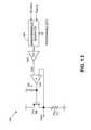
- FIG. 15illustrates an embodiment of an apparatus for impedance detection and adjustment for a configurable driver.
- a driversuch as the drivers illustrated in FIGS. 8A-12
- impedance detection and adjustmentis very important for effective operation.
- FIG. 15illustrates an embodiment of a mechanism to provide accurate adjustment of output impedance (resistance).
- a bias voltage input Vbias 1is provided to a gate of a first transistor (M 1 ) 1510 of a driver 1500 , where a first terminal of M 1 is coupled with voltage V DD and a second terminal of M 1 is coupled with a first end of a first variable resistor (R 1 ) 1512 and a bleeder current source (Ib) 1540 .
- a second end of R 1 1512is coupled with a first terminal of a transistor (M 3 ) 1516 , where a gate of M 3 is coupled with V DD and a second terminal of M 3 is coupled with a node for Vout.
- the Vout nodeis coupled with a voltage detector in the form of an analog to digital detector 1504 and to variable termination resistance (R 3 ) 1582 , and to a current mirror circuit comprising transistor 1570 coupled with transistor 1572 , transistor 1572 receiving a current from a current source (I) 1560 .
- the voltage detector in FIG. 15is a low-frequency analog to digital converter that may assist in the calibration process of impedance adjustment.
- the calibration proceduresmay be done in tandem to set the right calibrated values for Vbias 1 , Ib and R 1 , thus achieving the right swing voltage and impedance simultaneously.
- FIG. 16is an illustration of impedance characteristics of certain drivers.
- the impedance characteristics 1600 of a driverare shown to vary depending on the linear resistance of the impedance provided by the transistor and resistor of the driver, with increasing linear resistance providing a relationship closer to a linear (50-ohm) line 1650 , and non-linearity increasing with the effect of the transistor.
- fine-tuningmay be provided using a bleeder current source Ib.
- resistance R 1 1512should be much larger than the impedance of M 1 and vice versa.
- Dependence solely on R 1 1512 to provide the required impedanceresults in high power dissipation in M 1 1510 .
- a suitable division of impedance between R 1 and M 1is sought.
- the current characteristics of the driverare set by the swing requirements, such as provided in Figures.
- the bleeder current source Ib 1540provides additional flexibility in the tuning of the impedance of the transistor M 1 , providing an additional degree of freedom in this driver design.
- FIG. 17is an illustration of speed versus power tradeoff for an embodiment of a driver. As illustrated in the graph of frequency of operation versus power dissipation, a driver without termination resistance 1720 will require increasing power dissipation as frequency increases. However, a driver with termination resistance 1740 will require a generally small amount of power dissipation regardless of frequency.
- the drivers presented above as Type-I, Type-II, and Type-III driversgenerally consume power for high-states and consume no power (except for leakage current) in low states.
- FIG. 18Ais an illustration of an embodiment of a pulsing mechanism for a driver.
- a pulsing schemeis provided for low-speed operation.
- a driver 800is coupled with a pulsing mechanism 1850 .
- the driver 800is a Type-I driver as described above with regard to FIG. 8 .
- the pulsing mechanism 1850receives low speed data (such as data being transmitted at a frequency that that is below a certain threshold), where the low speed data is input to a delay element 1852 and to a first input of a NAND gate 1856 .
- a delayed data signal produced by the delay element 1852is received by an inverter 1854 , which provides a second input to the NAND gate element 1858 .
- the pulsing mechanism 1850includes multiplexer 1858 receiving a speed mode signal and receiving either a high-speed data input without alteration or a low speed data input that has been subject to pulsing by the pulsing mechanism 1850 .
- the pulsing mechanism 1850operates such that a high-transition is detected, and with a certain delay (based on the characteristics of the delay element 1852 other elements of the mechanism) the output is pulled low, providing a sufficient pulse for a receiver to detect the high bit.
- a certain delaybased on the characteristics of the delay element 1852 other elements of the mechanism
- the outputis pulled low, providing a sufficient pulse for a receiver to detect the high bit.
- the multiplexer 1858provides a bypass path to provide full and equal pulses in both high and low states for high-speed data.
- the transition point between low-speed and high-speed data rates for the purpose of using the pulsing mechanismmay be determined based on the current drain during high-state operation and the sensitivity of the receivers.
- FIG. 18Bis an illustration of signals generated by an embodiment of a pulsing mechanism of a driver.
- Low speed data 1860providing a full width bit signal, may result in excessive power dissipation by a driver.
- a pulsing mechanismsuch as pulsing mechanism 1850 illustrated in FIG. 18A , operates to return a signal pulse to low prior to the full width of a bit signal, such that the illustrated low-speed output data 1870 , which may be utilized to reduce power consumption in a driver circuit.
- Table 1compares certain performance characteristics for driver circuit technologies, including Type-I, Type-II, and Type-III driver technologies described above and illustrated in FIGS. 8-12 .
- V DD1.2 V
- source and termination impedancesare 50 ohms single-ended
- dynamic poweris not considered
- swing requirements for differential structuresare considered to be the same as single-ended structures because these are required to work at double the data rate.
- embodiments of Type-I, Type-II, and Type-III driversmay provide equal or better performance metrics among the parameters, which are commonly considered for a high-end driver.
- the power dissipation in pre-driversprovides additional power savings of embodiments of drivers in comparison with the conventional drivers.
- FIG. 19illustrates an embodiment of a driver apparatus for an interface between devices.
- a first devicesuch as a system 1910
- a second devicesuch as a memory 1960
- a channel 1950which may represent one or more channels between the first device and the second device.
- the systemis a system on chip (SOC) and the memory is a dynamic random access memory (DRAM).
- DRAMdynamic random access memory
- one or both of the system 1910 and memory 1960includes a configurable multi-mode driver.
- the system 1910includes a configurable multi-mode driver apparatus 1915 , which is coupled via the channel 1950 with a receiver apparatus 1970
- the memory 1960includes a configurable multi-mode driver 1965 , which is coupled via the channel 1950 with a receiver apparatus 1920 .
- the driver apparatus 1915 , the driver apparatus 1965 , or bothare a driver apparatus as illustrated in FIGS. 8 through 12 .
- driver apparatus 1915 of system 1910may include a particular termination resistance (R TERM ) 1917 and may provide a particular voltage swing (V SWING ) 1916
- receiver apparatus 1920may include a particular termination resistance 1921
- driver apparatus 1965 of memory 1960may include a particular termination resistance 1967 and voltage swing 1966
- receiver apparatus 1970may include a particular termination resistance 1971 . While each driver and receiver apparatus is illustrated as having a termination resistance, one or more of such terminations may be a small or zero resistance.
- the parameters of the drivers and receivers for devices 1910 and 1960such as the voltage swings and termination resistances, may be either symmetrical or asymmetrical between the devices depending on the implementation.
- the termination resistance 1917 provided for the driver apparatus 1915 of system 1910may not match a termination resistance 1967 for the driver apparatus 1965 of memory 1960
- a termination resistance 1921 provided for the receiver apparatus 1920 of system 1910may not match a termination resistance 1971 for the receiver apparatus 1970 of memory 1960
- a sensitivity of the receiver apparatus 1920may be different from a receiver sensitivity of the receiver apparatus 1970 .
- the receiver apparatus 1920 of the system 1910may include a valid termination in a read operation from the memory 1960 to the system 1910 , with data being driven by driver apparatus 1965 to receiver apparatus 1920 , the receiver apparatus 1920 of the system 1910 may include a valid termination.
- parameter information for the link between the system 1910 and memory 1960may be stored in on chip registers 1975 of the memory 1960 , if the memory 1960 is the secondary device.
- the systemmay include has a controller 1925 while the memory does not include a controller.
- the parameter information regarding voltage swings and termination resistanceis stored in the on chip registers for the memory 1960 to access.
- the driver apparatus 1915 and receiver apparatus 1920 of the system 1910may receive a supply voltage (V DD ) 1930
- driver apparatus 1965 and receiver apparatus 1970 of the memory 1960may receive a supply voltage 1980
- V REFthe voltage swing of a driver apparatus
- V REFa reference voltage
- the voltage swing of driver apparatus 1915 or 1965is referenced to a common system reference voltage (V REF ) 1957 , rather than to the supply voltage.
- the reference voltage 1957may be generated by an external source, such as reference voltage source 1955 , that provides the same reference voltage to each driver apparatus.
- the receiver apparatuses 1920 and 1970may also receive the reference voltage 1957 .
- the voltage swing 1916 of driver apparatus 1915 and voltage swing 1966 for driver apparatus 1965are functions of V REF .
- the voltage swing 1916 on driver apparatus 1915may be 2 times V REF while the voltage swing 1966 on driver 1965 may be 1.5 times V REF .
- voltage swingsare a function of V REF , independent of supply V DD .
- the voltage swingis thus independently configurable with a constant voltage supply.
- the configuration of the voltage swinghas no more than minimal effect on operation at an output node.
- the receiver apparatuses 1920 and 1970may also utilize the reference voltage 1957 .
- a reception sensitivity of receiver apparatus 1920 or 1970may be a function of the reference voltage.
- FIG. 20is a flowchart to illustrate an embodiment of a process for driving data from a first device to a second device.
- the first devicein a link between a first device and a second device 2000 , the first device includes a configurable driver apparatus and the second device includes a receiver apparatus.
- the receiver apparatusmay also configurable, including a configurable termination resistance.
- a determinationmay be made regarding the nature of the communications between the first device and the second device to identify correct parameters for the interface 2002 .
- the necessary parameters for the driver apparatus of the first device and the receiving apparatus of the second deviceare determined 2204 .
- parameters for a reverse connection of a driver apparatus of the second device and a receiving apparatus of the first deviceare also determined.
- parameters for an interfacemay be stored in one or more registers of a device, such as in a device, including a memory device, that does not include a controller.
- a termination resistance of the driver apparatus, the receiver apparatus, or bothis configured.
- the configuration of the termination resistancemay provide in part for configuration of a driver impedance 2006 .
- a voltage swing of the driver apparatus of the first deviceis configured 2208 .
- the configuration of the voltage swingis independent of a source voltage for the first device, and may operate to adjust the power dissipation of the driver apparatus.
- a bias voltageis provided for the driver apparatus 2010 .
- the establishment of the bias voltagemay include, for example, an apparatus as illustrated in FIG. 13 .
- a bias pointmay be adjusted through adjustment of a configurable current source of the driver apparatus 2012 .
- the application of a signal to the driver apparatusfurther includes determining a frequency of an input signal to the driver apparatus, and, if the frequency is below a threshold, changing the input signal to a pulse with a width that is shorter than a width of the input signal 2014 .
- the pulsing of the input signalmay include, for example the pulsing mechanism 1850 illustrated in FIG. 18A .
- the present inventionmay include various processes.
- the processes of the present inventionmay be performed by hardware components or may be embodied in computer-readable instructions, which may be used to cause a general purpose or special purpose processor or logic circuits programmed with the instructions to perform the processes.
- the processesmay be performed by a combination of hardware and software.
- Portions of the present inventionmay be provided as a computer program product, which may include a computer-readable storage medium having stored thereon computer program instructions, which may be used to program a computer (or other electronic devices) to perform a process according to the present invention.
- the computer-readable storage mediummay include, but is not limited to, floppy diskettes, optical disks, CD-ROMs (compact disk read-only memory), and magneto-optical disks, ROMs (read-only memory), RAMs (random access memory), EPROMs (erasable programmable read-only memory), EEPROMs (electrically-erasable programmable read-only memory), magnet or optical cards, flash memory, or other type of media/computer-readable medium suitable for storing electronic instructions.
- the present inventionmay also be downloaded as a computer program product, wherein the program may be transferred from a remote computer to a requesting computer.
- element Amay be directly coupled to element B or be indirectly coupled through, for example, element C.
- a component, feature, structure, process, or characteristic A“causes” a component, feature, structure, process, or characteristic B, it means that “A” is at least a partial cause of “B” but that there may also be at least one other component, feature, structure, process, or characteristic that assists in causing “B.” If the specification indicates that a component, feature, structure, process, or characteristic “may”, “might”, or “could” be included, that particular component, feature, structure, process, or characteristic is not required to be included. If the specification refers to “a” or “an” element, this does not mean there is only one of the described elements.
- An embodimentis an implementation or example of the invention.
- Reference in the specification to “an embodiment,” “one embodiment,” “some embodiments,” or “other embodiments”means that a particular feature, structure, or characteristic described in connection with the embodiments is included in at least some embodiments, but not necessarily all embodiments.
- the various appearances of “an embodiment,” “one embodiment,” or “some embodiments”are not necessarily all referring to the same embodiments. It should be appreciated that in the foregoing description of exemplary embodiments of the invention, various features of the invention are sometimes grouped together in a single embodiment, figure, or description thereof for the purpose of streamlining the disclosure and aiding in the understanding of one or more of the various inventive aspects.
Landscapes
- Engineering & Computer Science (AREA)
- Computer Hardware Design (AREA)
- Physics & Mathematics (AREA)
- Computing Systems (AREA)
- General Engineering & Computer Science (AREA)
- Mathematical Physics (AREA)
- Computer Networks & Wireless Communication (AREA)
- Signal Processing (AREA)
- Power Engineering (AREA)
- Logic Circuits (AREA)
- Dc Digital Transmission (AREA)
Abstract
Description
Z0=R1//R3 [1]
Vdriverout=(R3//Rt)/(R3//Rt+R1) [2]
- where // refers to resistors in parallel and Rt is assumed to match channel characteristic impedance
| TABLE 1 |
| Performance comparison between different drivers |
| Power | Voltage | |||
| Driver | Dissi- | Data rate | swing pro- | Termination |
| Structure | pation | requirements | grammability | Control |
| Differential | 1x | 2x | No | Yes |
| voltage-mode | ||||
| Single-ended | 2x | 1x | No | Yes |
| voltage mode | ||||
| Differential | 1x | 2x | Yes | No |
| current-mode | ||||
| Single-ended | 2x | 1x | Yes | Yes |
| current-mode | ||||
| Type-I voltage- | 1.5x | 1x | Yes | Yes |
| mode driver | ||||
| Type-II mixed- | 1x | 1x | Yes | Yes |
| mode driver | ||||
| Type-III mixed- | 1x | 1x | Yes | Yes |
| mode driver | ||||
Claims (55)
Priority Applications (9)
| Application Number | Priority Date | Filing Date | Title |
|---|---|---|---|
| US13/174,630US9071243B2 (en) | 2011-06-30 | 2011-06-30 | Single ended configurable multi-mode driver |
| CN201280025948.1ACN103582853B (en) | 2011-06-30 | 2012-06-22 | Single-ended configurable multi-mode driver |
| PCT/US2012/043770WO2013003231A2 (en) | 2011-06-30 | 2012-06-22 | Single-ended configurable multi-mode driver |
| KR1020147002147AKR101965788B1 (en) | 2011-06-30 | 2012-06-22 | Single-ended configurable multi-mode driver |
| JP2014518871AJP5969605B2 (en) | 2011-06-30 | 2012-06-22 | Single-end configurable multimode driver |
| EP12803660.5AEP2726950A4 (en) | 2011-06-30 | 2012-06-22 | Single-ended configurable multi-mode driver |
| TW101123336ATWI593232B (en) | 2011-06-30 | 2012-06-28 | Single-ended configurable multi-mode driver |
| US14/717,856US9240784B2 (en) | 2011-06-30 | 2015-05-20 | Single-ended configurable multi-mode driver |
| JP2016057155AJP6140860B2 (en) | 2011-06-30 | 2016-03-22 | Single-end configurable multimode driver |
Applications Claiming Priority (1)
| Application Number | Priority Date | Filing Date | Title |
|---|---|---|---|
| US13/174,630US9071243B2 (en) | 2011-06-30 | 2011-06-30 | Single ended configurable multi-mode driver |
Related Child Applications (1)
| Application Number | Title | Priority Date | Filing Date |
|---|---|---|---|
| US14/717,856ContinuationUS9240784B2 (en) | 2011-06-30 | 2015-05-20 | Single-ended configurable multi-mode driver |
Publications (2)
| Publication Number | Publication Date |
|---|---|
| US20130002301A1 US20130002301A1 (en) | 2013-01-03 |
| US9071243B2true US9071243B2 (en) | 2015-06-30 |
Family
ID=47389998
Family Applications (2)
| Application Number | Title | Priority Date | Filing Date |
|---|---|---|---|
| US13/174,630ActiveUS9071243B2 (en) | 2011-06-30 | 2011-06-30 | Single ended configurable multi-mode driver |
| US14/717,856ActiveUS9240784B2 (en) | 2011-06-30 | 2015-05-20 | Single-ended configurable multi-mode driver |
Family Applications After (1)
| Application Number | Title | Priority Date | Filing Date |
|---|---|---|---|
| US14/717,856ActiveUS9240784B2 (en) | 2011-06-30 | 2015-05-20 | Single-ended configurable multi-mode driver |
Country Status (7)
| Country | Link |
|---|---|
| US (2) | US9071243B2 (en) |
| EP (1) | EP2726950A4 (en) |
| JP (2) | JP5969605B2 (en) |
| KR (1) | KR101965788B1 (en) |
| CN (1) | CN103582853B (en) |
| TW (1) | TWI593232B (en) |
| WO (1) | WO2013003231A2 (en) |
Cited By (3)
| Publication number | Priority date | Publication date | Assignee | Title |
|---|---|---|---|---|
| US20170237426A1 (en)* | 2016-02-16 | 2017-08-17 | Infineon Technologies Ag | Device and method for internal reset signal generation |
| US10079603B1 (en)* | 2018-04-08 | 2018-09-18 | Nxp B.V. | Configurable, multi-functional driver circuit |
| US11314462B2 (en)* | 2020-08-21 | 2022-04-26 | Samsung Electronics Co., Ltd. | Interface circuit and system including same |
Families Citing this family (32)
| Publication number | Priority date | Publication date | Assignee | Title |
|---|---|---|---|---|
| US9071243B2 (en) | 2011-06-30 | 2015-06-30 | Silicon Image, Inc. | Single ended configurable multi-mode driver |
| KR101958394B1 (en)* | 2011-11-08 | 2019-03-14 | 에스케이하이닉스 주식회사 | Semiconductor device |
| US8604838B2 (en)* | 2011-12-12 | 2013-12-10 | Texas Instruments Incorporated | Comparator with improved time constant |
| US8885435B2 (en) | 2012-09-18 | 2014-11-11 | Silicon Image, Inc. | Interfacing between integrated circuits with asymmetric voltage swing |
| US9715467B2 (en) | 2012-11-26 | 2017-07-25 | Rambus Inc. | Calibration protocol for command and address bus voltage reference in low-swing single-ended signaling |
| US9306563B2 (en)* | 2013-02-19 | 2016-04-05 | Lattice Semiconductor Corporation | Configurable single-ended driver |
| CN104036812B (en)* | 2013-03-04 | 2017-04-12 | 德克萨斯仪器股份有限公司 | Comparator with improved time constant |
| US9525571B2 (en) | 2013-03-05 | 2016-12-20 | Lattice Semiconductor Corporation | Calibration of single-ended high-speed interfaces |
| JP6231793B2 (en)* | 2013-07-10 | 2017-11-15 | ローム株式会社 | Differential signal transmission circuit |
| US9306555B2 (en)* | 2013-12-20 | 2016-04-05 | Intel Corporation | Apparatus and method to achieve CPAD mitigation effects |
| US8970254B1 (en)* | 2014-03-03 | 2015-03-03 | Qualcomm Incorporated | Systems and methods for frequency detection |
| US9264263B2 (en)* | 2014-04-21 | 2016-02-16 | Qualcomm Incorporated | Serdes voltage-mode driver with skew correction |
| US9431961B2 (en)* | 2014-10-29 | 2016-08-30 | Qualcomm Incorporated | Phase shifting mixer |
| KR102001693B1 (en) | 2014-11-20 | 2019-07-18 | 에스케이하이닉스 주식회사 | Data transmitter |
| US20160162214A1 (en)* | 2014-12-08 | 2016-06-09 | James A McCall | Adjustable low swing memory interface |
| US9698813B2 (en)* | 2015-12-01 | 2017-07-04 | Mediatek Inc. | Input buffer and analog-to-digital converter |
| US9621140B1 (en)* | 2016-01-15 | 2017-04-11 | Allegro Microsystems, Llc | Electronic circuit for driving an output current signal and method of driving the output current signal from the electronic circuit to achieve an altered transition of the output current signal |
| EP3513723B1 (en) | 2016-09-16 | 2022-12-21 | Nec Corporation | Personal authentication device, personal authentication method, and recording medium |
| WO2019087602A1 (en)* | 2017-11-02 | 2019-05-09 | ソニーセミコンダクタソリューションズ株式会社 | Electronic circuit and electronic apparatus |
| CN110061731B (en)* | 2018-01-19 | 2025-05-30 | 综合器件技术公司 | High signal voltage tolerance in single-ended memory interfaces |
| US10411703B1 (en)* | 2018-06-05 | 2019-09-10 | Samsung Electronics Co., Ltd. | Impedance matched clock driver with amplitude control |
| US11409354B2 (en)* | 2019-04-22 | 2022-08-09 | Micron Technology, Inc. | Multi-voltage operation for driving a multi-mode channel |
| US10896723B2 (en)* | 2019-04-30 | 2021-01-19 | Ambient Scientific Inc. | Signal communication circuit implementing receiver and transmitter circuits |
| CN110187732B (en)* | 2019-05-22 | 2020-12-08 | 清华大学 | A hybrid voltage-mode and current-mode PAM-4 high-speed drive circuit |
| WO2021085791A1 (en)* | 2019-10-29 | 2021-05-06 | 한국과학기술원 | Feedback-based on-die termination circuit |
| TWI728624B (en)* | 2019-12-26 | 2021-05-21 | 創意電子股份有限公司 | Voltage mode signal transmitter |
| US11233506B1 (en) | 2020-07-28 | 2022-01-25 | Qualcomm Incorporated | Hybrid driver with a wide output amplitude range |
| US11378992B2 (en) | 2020-07-28 | 2022-07-05 | Qualcomm Incorporated | Hybrid voltage regulator with a wide regulated voltage range |
| WO2022026059A1 (en)* | 2020-07-28 | 2022-02-03 | Qualcomm Incorporated | Hybrid driver with a wide output amplitude range |
| CN112088406B (en) | 2020-08-06 | 2023-10-03 | 长江存储科技有限责任公司 | Multi-die peak power management for three-dimensional memory |
| US12160256B2 (en)* | 2021-12-22 | 2024-12-03 | Xilinx, Inc. | DAC-based transmit driver architecture with improved bandwidth |
| EP4346110A1 (en)* | 2022-09-29 | 2024-04-03 | Nxp B.V. | A transmitter circuit |
Citations (125)
| Publication number | Priority date | Publication date | Assignee | Title |
|---|---|---|---|---|
| US5982210A (en) | 1994-09-02 | 1999-11-09 | Sun Microsystems, Inc. | PLL system clock generator with instantaneous clock frequency shifting |
| US6130563A (en) | 1997-09-10 | 2000-10-10 | Integrated Device Technology, Inc. | Output driver circuit for high speed digital signal transmission |
| US6288563B1 (en) | 1998-12-31 | 2001-09-11 | Intel Corporation | Slew rate control |
| US20020061016A1 (en) | 1998-08-05 | 2002-05-23 | Vitesse Semiconductor Corporation | High speed cross point switch routing circuit with word-synchronous serial back plane |
| US6397042B1 (en) | 1998-03-06 | 2002-05-28 | Texas Instruments Incorporated | Self test of an electronic device |
| US20030074515A1 (en) | 2001-10-11 | 2003-04-17 | International Business Machines | System for supporting both serial and parallel storage devices on a connector |
| US6560290B2 (en) | 1998-01-20 | 2003-05-06 | Silicon Image, Inc. | CMOS driver and on-chip termination for gigabaud speed data communication |
| US20030105896A1 (en) | 2001-11-21 | 2003-06-05 | Interdigital Technology Corporation | Base station having a hybrid parallel/serial bus interface |
| US20030218477A1 (en) | 2002-05-24 | 2003-11-27 | Samsung Electronics Co., Ltd. | Circuit and method for controlling on-die signal termination |
| US6677793B1 (en) | 2003-02-03 | 2004-01-13 | Lsi Logic Corporation | Automatic delay matching circuit for data serializer |
| US6714465B2 (en) | 2001-10-23 | 2004-03-30 | Samsung Electronics Co., Ltd. | Memory device and process for improving the state of a termination |
| US6718473B1 (en) | 2000-09-26 | 2004-04-06 | Sun Microsystems, Inc. | Method and apparatus for reducing power consumption |
| US20040098545A1 (en) | 2002-11-15 | 2004-05-20 | Pline Steven L. | Transferring data in selectable transfer modes |
| US6748469B1 (en) | 2001-01-31 | 2004-06-08 | Lsi Logic Corporation | Parallel/serial SCSI with legacy support |
| CN1538703A (en) | 2003-02-26 | 2004-10-20 | ���ǵ�����ʽ���� | Hybrid data transmission device and method suitable for high-performance wireless local area network |
| US20050007145A1 (en) | 2003-07-10 | 2005-01-13 | International Business Machines Corporation | Thevenins receiver |
| US20050030200A1 (en) | 2003-05-30 | 2005-02-10 | Holt Michael D. | Low power telemetry system and method |
| US6859107B1 (en) | 2001-09-05 | 2005-02-22 | Silicon Image, Inc. | Frequency comparator with hysteresis between locked and unlocked conditions |
| US6862246B2 (en) | 2002-06-05 | 2005-03-01 | Elpida Memory, Inc. | Semiconductor apparatus which prevents generating noise and being influenced by noise |
| US20050052200A1 (en) | 2003-09-08 | 2005-03-10 | Nguyen Huy M. | Calibration methods and circuits for optimized on-die termination |
| US6870419B1 (en)* | 1997-08-29 | 2005-03-22 | Rambus Inc. | Memory system including a memory device having a controlled output driver characteristic |
| US6901126B1 (en) | 2000-06-30 | 2005-05-31 | Texas Instruments Incorporated | Time division multiplex data recovery system using close loop phase and delay locked loop |
| US20050174153A1 (en) | 2004-02-09 | 2005-08-11 | Nec Electronics Corporation | Fractional frequency divider circuit and data transmission apparatus using the same |
| US20050242851A1 (en) | 2004-04-29 | 2005-11-03 | Booth Richard V | Signal generator with selectable mode control |
| US20060017470A1 (en) | 2004-07-21 | 2006-01-26 | Park Sung K | Low power high performance inverter circuit |
| US6996749B1 (en) | 2003-11-13 | 2006-02-07 | Intel Coporation | Method and apparatus for providing debug functionality in a buffered memory channel |
| US20060034394A1 (en) | 2004-08-10 | 2006-02-16 | Petre Popescu | Circuit for adaptive sampling edge position control and a method therefor |
| US7032058B2 (en) | 1999-10-19 | 2006-04-18 | Rambus Inc. | Apparatus and method for topography dependent signaling |
| US7036032B2 (en) | 2002-01-04 | 2006-04-25 | Ati Technologies, Inc. | System for reduced power consumption by phase locked loop and method thereof |
| US7089444B1 (en) | 2003-09-24 | 2006-08-08 | Altera Corporation | Clock and data recovery circuits |
| US20060188043A1 (en) | 2005-01-20 | 2006-08-24 | Zerbe Jared L | High-speed signaling systems with adaptable pre-emphasis and equalization |
| US20060192622A1 (en) | 2005-02-28 | 2006-08-31 | Kawasaki Microelectronics, Inc. | Semiconductor integrated circuit |
| US7102446B1 (en) | 2005-02-11 | 2006-09-05 | Silicon Image, Inc. | Phase lock loop with coarse control loop having frequency lock detector and device including same |
| EP0834814B1 (en) | 1996-10-02 | 2006-09-13 | Fujitsu Limited | Signal-transfer system and semiconductor device for high speed data transfer |
| US7133648B1 (en) | 2003-06-03 | 2006-11-07 | Xilinx, Inc. | Bidirectional multi-gigabit transceiver |
| US7155617B2 (en) | 2002-08-01 | 2006-12-26 | Texas Instruments Incorporated | Methods and systems for performing dynamic power management via frequency and voltage scaling |
| US20070035336A1 (en) | 2005-02-09 | 2007-02-15 | Seong-Hoon Lee | Clock generating circuit with multiple modes of operation |
| US7191371B2 (en) | 2002-04-09 | 2007-03-13 | Internatioanl Business Machines Corporation | System and method for sequential testing of high speed serial link core |
| US20070080718A1 (en) | 2003-12-17 | 2007-04-12 | Stojanovic Vladimir M | High speed signaling system with adaptive transmit pre-emphasis |
| US7209178B1 (en) | 1999-09-21 | 2007-04-24 | Samsung Electronics, Co., Ltd. | Optical transfer system having a transmitter and a receiver |
| CN1959801A (en) | 2005-11-10 | 2007-05-09 | 威盛电子股份有限公司 | dual purpose drive |
| US20070127614A1 (en) | 2005-12-07 | 2007-06-07 | Nec Electronics Corporation | Communication device |
| US7254797B2 (en) | 2004-09-30 | 2007-08-07 | Rambus Inc. | Input/output cells with localized clock routing |
| US20070230513A1 (en) | 2006-03-28 | 2007-10-04 | Talbot Gerald R | Transmitter voltage and receiver time margining |
| US20070252624A1 (en) | 2006-04-28 | 2007-11-01 | Young-Soo Sohn | Output driver having pre-emphasis capability |
| US20070281741A1 (en) | 2006-05-30 | 2007-12-06 | Pixart Imaging Inc. | Data communication system |
| US7308058B2 (en) | 2003-10-27 | 2007-12-11 | Rambus Inc. | Transparent multi-mode PAM interface |
| US7345602B2 (en) | 2005-07-28 | 2008-03-18 | Nec Electronics Corporation | Pre-emphasis circuit |
| JP2008092285A (en) | 2006-10-02 | 2008-04-17 | Nec Corp | Mobile communication terminal and control method therefor |
| US20080123792A1 (en) | 2006-11-27 | 2008-05-29 | Edoardo Prete | Apparatus and method for transmitting signals over a signal line |
| US20080122488A1 (en) | 2006-11-23 | 2008-05-29 | Yi-Lin Chen | Output driving circuit |
| US7389097B2 (en) | 1999-07-14 | 2008-06-17 | Fujitsu Limited | Receiver, transceiver circuit, signal transmission method, and signal transmission system |
| US7389190B2 (en) | 2003-09-09 | 2008-06-17 | Advantest Corporation | Testing apparatus for testing a device under test and comparator circuit and calibration apparatus for the testing apparatus |
| US20080164905A1 (en) | 2003-10-23 | 2008-07-10 | Nec Electronics Corporation | I/O interface circuit of intergrated circuit |
| US7406118B2 (en) | 2003-09-11 | 2008-07-29 | Xilinx, Inc. | Programmable logic device including programmable multi-gigabit transceivers |
| US7447278B2 (en) | 2003-05-21 | 2008-11-04 | International Business Machines Corporation | Apparatus for transmitting and receiving data |
| US7450535B2 (en) | 2005-12-01 | 2008-11-11 | Rambus Inc. | Pulsed signaling multiplexer |
| US20080284466A1 (en) | 2007-05-18 | 2008-11-20 | Cranford Jr Hayden Clavie | Driver Circuit |
| US20080310491A1 (en) | 2007-06-12 | 2008-12-18 | Aliazam Abbasfar | Multi-mode transmitter |
| US7475273B2 (en) | 2001-11-21 | 2009-01-06 | Interdigital Technology Corporation | Hybrid parallel/serial bus interface |
| US7493095B2 (en) | 2003-09-11 | 2009-02-17 | Xilinx, Inc. | PMA RX in coarse loop for high speed sampling |
| US7496774B2 (en) | 2004-06-04 | 2009-02-24 | Broadcom Corporation | Method and system for generating clocks for standby mode operation in a mobile communication device |
| US20090059712A1 (en) | 2007-08-29 | 2009-03-05 | Hyung-Dong Lee | Output driver |
| US7501851B2 (en) | 2006-05-26 | 2009-03-10 | Pmc Sierra Inc. | Configurable voltage mode transmitted architecture with common-mode adjustment and novel pre-emphasis |
| US7505512B1 (en) | 2005-05-05 | 2009-03-17 | Xilinx , Inc. | Method and apparatus for combining statistical eye channel compliance methods with linear continuous-time equalization |
| US20090153219A1 (en) | 2007-12-17 | 2009-06-18 | Charles Qingle Wu | Replica bias circuit for high speed low voltage common mode driver |
| US7555048B1 (en) | 2003-11-24 | 2009-06-30 | Neascape, Inc. | High-speed single-ended interface |
| US20090182912A1 (en) | 2008-01-11 | 2009-07-16 | Korea Advanced Institute Of Science And Technology | High Speed Serializing-Deserializing System and Method |
| US7583753B2 (en) | 2004-08-16 | 2009-09-01 | Samsung Electronics Co., Ltd. | Methods and transmitters for loop-back adaptive pre-emphasis data transmission |
| JP2009225406A (en) | 2008-03-19 | 2009-10-01 | Seiko Epson Corp | Integrated circuit device, electro-optical device and electronic device |
| US20090256585A1 (en)* | 2008-04-10 | 2009-10-15 | Kwon Yong Kee | Data line termination circuit |
| US7617064B2 (en) | 2005-04-12 | 2009-11-10 | Analog Devices, Inc. | Self-test circuit for high-definition multimedia interface integrated circuits |
| US20090289668A1 (en)* | 2008-05-23 | 2009-11-26 | Arm Limited | Output driver circuit for an integrated circuit |
| US20090327565A1 (en) | 2008-06-27 | 2009-12-31 | Rambus Inc. | Bimodal memory controller |
| US20100060316A1 (en) | 2008-09-05 | 2010-03-11 | Hynix Semiconductor, Inc. | Calibration circuit, on die termination device and semiconductor memory device using the same |
| US7697649B2 (en) | 2005-08-24 | 2010-04-13 | Samsung Electronics Co., Ltd. | Circuit for measuring an eye size of data, and method of measuring the eye size of data |
| US20100097094A1 (en)* | 2008-10-21 | 2010-04-22 | Samsung Electronics Co., Ltd. | Output circuit having variable output voltage swing level |
| US20100103994A1 (en) | 2006-12-13 | 2010-04-29 | Frans Yohan U | Interface With Variable Data Rate |
| US20100127751A1 (en) | 2008-11-24 | 2010-05-27 | Maung-Wai Lin | Level shifter adaptive for use in a power-saving operation mode |
| US20100157644A1 (en) | 2008-12-19 | 2010-06-24 | Unity Semiconductor Corporation | Configurable memory interface to provide serial and parallel access to memories |
| US20100164539A1 (en) | 2008-12-31 | 2010-07-01 | Ganesh Balamurugan | System and apparatus of reconfigurable transceiver design for multi-mode signaling |
| US7840727B2 (en) | 2005-07-28 | 2010-11-23 | Nec Electronics Corporation | Serial-to-parallel conversion/parallel-to-serial conversion/ FIFO unified circuit |
| US20100296566A1 (en) | 2007-05-24 | 2010-11-25 | Rambus Inc. | Method and apparatus for determining a calibration signal |
| US7898288B2 (en) | 2006-12-07 | 2011-03-01 | Integrated Device Technology, Inc. | Input termination for delay locked loop feedback with impedance matching |
| US20110050280A1 (en)* | 2009-08-31 | 2011-03-03 | John Maddux | Methods and systems to calibrate push-pull drivers |
| US7916560B2 (en) | 2007-07-12 | 2011-03-29 | Hynix Semiconductor Inc. | Semiconductor memory device |
| US20110099410A1 (en) | 2007-07-09 | 2011-04-28 | John Yin | Clock data recovery and synchronization in interconnected devices |
| US7945805B2 (en) | 2006-12-13 | 2011-05-17 | International Business Machines Corporation | Architecture for a physical interface of a high speed front side bus |
| CN102075462A (en) | 2009-09-29 | 2011-05-25 | 雷凌科技股份有限公司 | Multimode Ethernet line driver |
| US20110196997A1 (en) | 2010-02-11 | 2011-08-11 | Ruberg Alan T | Hybrid interface for serial and parallel communication |
| US20110222594A1 (en) | 2006-12-05 | 2011-09-15 | Rambus Inc. | Methods and Circuits for Asymmetric Distribution of Channel Equalization Between Devices |
| US20110235763A1 (en) | 2009-01-12 | 2011-09-29 | Rambus Inc. | Signaling system with asymmetrically-managed timing calibration |
| US8051228B2 (en) | 2008-11-13 | 2011-11-01 | International Business Machines Corporation | Physical interface macros (PHYS) supporting heterogeneous electrical properties |
| US8050317B2 (en) | 2007-01-19 | 2011-11-01 | Samsung Electronics Co., Ltd. | Receiver with equalizer and method of operation |
| US8135100B2 (en) | 2008-08-20 | 2012-03-13 | International Business Machines Corporation | Adaptive clock and equalization control systems and methods for data receivers in communications systems |
| US20120072759A1 (en) | 2010-09-21 | 2012-03-22 | Ipgoal Microelectronics (Sichuan) Co., Ltd. | Timing Error Correction System and Method |
| US8208815B1 (en) | 2006-11-30 | 2012-06-26 | Marvell International Ltd. | Bit accurate upstream burst transmission phase method for reducing burst data arrival variation |
| USRE43539E1 (en) | 2001-12-19 | 2012-07-24 | Elpida Memory, Inc. | Output buffer circuit and integrated semiconductor circuit device with such output buffer circuit |
| US8275030B2 (en) | 2003-12-17 | 2012-09-25 | Rambus Inc. | Signaling system with selectively-inhibited adaptive equalization |
| US8279976B2 (en) | 2007-10-30 | 2012-10-02 | Rambus Inc. | Signaling with superimposed differential-mode and common-mode signals |
| US8290028B2 (en) | 2007-06-01 | 2012-10-16 | Renesas Electronics Corporation | Input/output circuit |
| US20130002301A1 (en) | 2011-06-30 | 2013-01-03 | Srikanth Gondi | Single-ended configurable multi-mode driver |
| US20130038346A1 (en) | 2008-03-31 | 2013-02-14 | Micron Technology, Inc. | Apparatus and method for signal transmission over a channel |
| US8416001B2 (en) | 2011-04-08 | 2013-04-09 | Altera Corporation | Techniques for reducing duty cycle distortion in periodic signals |
| US8415980B2 (en) | 2011-06-28 | 2013-04-09 | Microsoft Corporation | Serializing transmitter |
| US20130093433A1 (en) | 2007-03-20 | 2013-04-18 | Rambus Inc. | Integrated Circuit Having Receiver Jitter Tolerance ("JTOL") Measurement |
| US20130148448A1 (en) | 2002-08-23 | 2013-06-13 | Elpida Memory, Inc. | Memory system and data transmission method |
| US8520765B2 (en) | 2008-08-29 | 2013-08-27 | Sony Corporation | Information processing apparatus, signal transmission method and decoding method |
| US8520348B2 (en) | 2011-12-22 | 2013-08-27 | Lsi Corporation | High-swing differential driver using low-voltage transistors |
| US8578222B2 (en) | 2011-02-17 | 2013-11-05 | Qualcomm Incorporated | SerDes power throttling as a function of detected error rate |
| US8593885B2 (en) | 2011-03-18 | 2013-11-26 | Rambus Inc. | Staggered mode transitions in a segmented interface |
| US8624641B1 (en) | 2010-11-03 | 2014-01-07 | Pmc-Sierra, Inc. | Apparatus and method for driving a transistor |
| US8650429B1 (en) | 2009-01-31 | 2014-02-11 | Xilinx, Inc. | Clock phase alignment |
| US20140107997A1 (en) | 2010-04-19 | 2014-04-17 | Altera Corporation | Simulation Tool for High-Speed Communications Links |
| US8705605B1 (en) | 2011-11-03 | 2014-04-22 | Altera Corporation | Technique for providing loopback testing with single stage equalizer |
| US20140149775A1 (en) | 2011-07-12 | 2014-05-29 | Rambus Inc. | Dynamically changing data access bandwidth by selectively enabling and disabling data links |
| US8760977B2 (en) | 2011-04-28 | 2014-06-24 | Lsi Corporation | Systems and methods for data write loopback based timing control |
| US8779819B1 (en) | 2012-04-30 | 2014-07-15 | Pmc-Sierra Us, Inc. | Transmitter output impedance calibration for output rise and fall time equalization and edge rate control |
| US20140211862A1 (en) | 2011-05-25 | 2014-07-31 | The Silanna Group Pty Ltd. | Usb isolator integrated circuit with usb 2.0 high speed mode and automatic speed detection |
| US8832487B2 (en) | 2011-06-28 | 2014-09-09 | Microsoft Corporation | High-speed I/O data system |
| US8861667B1 (en) | 2002-07-12 | 2014-10-14 | Rambus Inc. | Clock data recovery circuit with equalizer clock calibration |
| US8879618B2 (en) | 2010-09-13 | 2014-11-04 | Semtech Canada Corporation | Decision feedback equalizer and transceiver |
| US8878792B2 (en) | 2009-08-13 | 2014-11-04 | Samsung Electronics Co., Ltd. | Clock and data recovery circuit of a source driver and a display device |
| US8886840B2 (en) | 2002-08-07 | 2014-11-11 | Broadcom Corporation | System and method for implementing a single chip having a multiple sub-layer PHY |
| US8930647B1 (en) | 2011-04-06 | 2015-01-06 | P4tents1, LLC | Multiple class memory systems |
Family Cites Families (16)
| Publication number | Priority date | Publication date | Assignee | Title |
|---|---|---|---|---|
| JPH06104936A (en)* | 1992-09-18 | 1994-04-15 | Hitachi Ltd | Signal transmission method and signal transmission circuit |
| KR0138327B1 (en) | 1994-12-19 | 1998-06-15 | 김광호 | Data transmitting apparatus |
| JP3487723B2 (en)* | 1996-09-19 | 2004-01-19 | 沖電気工業株式会社 | Interface circuit and signal transmission method |
| US5949254A (en)* | 1996-11-26 | 1999-09-07 | Micron Technology, Inc. | Adjustable output driver circuit |
| US5838177A (en)* | 1997-01-06 | 1998-11-17 | Micron Technology, Inc. | Adjustable output driver circuit having parallel pull-up and pull-down elements |
| JP3967002B2 (en)* | 1997-09-11 | 2007-08-29 | 株式会社ルネサステクノロジ | Semiconductor integrated circuit |
| US6792494B2 (en) | 2001-03-30 | 2004-09-14 | Intel Corporation | Apparatus and method for parallel and serial PCI hot plug signals |
| JP3996540B2 (en)* | 2003-04-04 | 2007-10-24 | エルピーダメモリ株式会社 | Signal transmission system |
| JP4428504B2 (en)* | 2003-04-23 | 2010-03-10 | 株式会社ルネサステクノロジ | Semiconductor integrated circuit device |
| JP2006060751A (en)* | 2004-08-24 | 2006-03-02 | Ricoh Co Ltd | OUTPUT DEVICE, DIFFERENTIAL OUTPUT DEVICE, SEMICONDUCTOR LASER MODULATION DRIVE DEVICE, IMAGE FORMING DEVICE, AND ELECTRONIC DEVICE |
| JP2007306267A (en)* | 2006-05-11 | 2007-11-22 | Matsushita Electric Ind Co Ltd | Semiconductor transceiver system, memory card and memory card host device |
| JP2008258816A (en)* | 2007-04-03 | 2008-10-23 | Matsushita Electric Ind Co Ltd | Semiconductor device, driving capability switching method for semiconductor device, and system including semiconductor device |
| DE102007054307A1 (en) | 2007-11-08 | 2009-05-20 | Siemens Ag | Method and device for performing a frequency analysis of an alternating voltage signal, in particular on a power supply line |
| US8880928B2 (en) | 2008-04-11 | 2014-11-04 | Thinklogical, Llc | Multirate transmission system and method for parallel input data |
| JP5372464B2 (en)* | 2008-10-17 | 2013-12-18 | 株式会社メガチップス | Differential output buffer |
| FR2959367A1 (en) | 2010-04-21 | 2011-10-28 | St Microelectronics Sa | BUFFER CIRCUIT FOR HIGH VALUE CAPACITIVE LOAD |
- 2011
- 2011-06-30USUS13/174,630patent/US9071243B2/enactiveActive
- 2012
- 2012-06-22EPEP12803660.5Apatent/EP2726950A4/ennot_activeWithdrawn
- 2012-06-22CNCN201280025948.1Apatent/CN103582853B/enactiveActive
- 2012-06-22WOPCT/US2012/043770patent/WO2013003231A2/enactiveApplication Filing
- 2012-06-22KRKR1020147002147Apatent/KR101965788B1/enactiveActive
- 2012-06-22JPJP2014518871Apatent/JP5969605B2/enactiveActive
- 2012-06-28TWTW101123336Apatent/TWI593232B/enactive
- 2015
- 2015-05-20USUS14/717,856patent/US9240784B2/enactiveActive
- 2016
- 2016-03-22JPJP2016057155Apatent/JP6140860B2/enactiveActive
Patent Citations (134)
| Publication number | Priority date | Publication date | Assignee | Title |
|---|---|---|---|---|
| US5982210A (en) | 1994-09-02 | 1999-11-09 | Sun Microsystems, Inc. | PLL system clock generator with instantaneous clock frequency shifting |
| EP0834814B1 (en) | 1996-10-02 | 2006-09-13 | Fujitsu Limited | Signal-transfer system and semiconductor device for high speed data transfer |
| US6870419B1 (en)* | 1997-08-29 | 2005-03-22 | Rambus Inc. | Memory system including a memory device having a controlled output driver characteristic |
| US6130563A (en) | 1997-09-10 | 2000-10-10 | Integrated Device Technology, Inc. | Output driver circuit for high speed digital signal transmission |
| US6560290B2 (en) | 1998-01-20 | 2003-05-06 | Silicon Image, Inc. | CMOS driver and on-chip termination for gigabaud speed data communication |
| US6397042B1 (en) | 1998-03-06 | 2002-05-28 | Texas Instruments Incorporated | Self test of an electronic device |
| US20020061016A1 (en) | 1998-08-05 | 2002-05-23 | Vitesse Semiconductor Corporation | High speed cross point switch routing circuit with word-synchronous serial back plane |
| US6288563B1 (en) | 1998-12-31 | 2001-09-11 | Intel Corporation | Slew rate control |
| US7389097B2 (en) | 1999-07-14 | 2008-06-17 | Fujitsu Limited | Receiver, transceiver circuit, signal transmission method, and signal transmission system |
| US7209178B1 (en) | 1999-09-21 | 2007-04-24 | Samsung Electronics, Co., Ltd. | Optical transfer system having a transmitter and a receiver |
| US7032058B2 (en) | 1999-10-19 | 2006-04-18 | Rambus Inc. | Apparatus and method for topography dependent signaling |
| US6901126B1 (en) | 2000-06-30 | 2005-05-31 | Texas Instruments Incorporated | Time division multiplex data recovery system using close loop phase and delay locked loop |
| US6718473B1 (en) | 2000-09-26 | 2004-04-06 | Sun Microsystems, Inc. | Method and apparatus for reducing power consumption |
| US6748469B1 (en) | 2001-01-31 | 2004-06-08 | Lsi Logic Corporation | Parallel/serial SCSI with legacy support |
| US6859107B1 (en) | 2001-09-05 | 2005-02-22 | Silicon Image, Inc. | Frequency comparator with hysteresis between locked and unlocked conditions |
| US7203260B2 (en) | 2001-09-05 | 2007-04-10 | Silicon Image, Inc. | Tracked 3X oversampling receiver |
| US6888417B2 (en) | 2001-09-05 | 2005-05-03 | Silicon Image, Inc. | Voltage controlled oscillator |
| US6876240B2 (en) | 2001-09-05 | 2005-04-05 | Silicon Image, Inc. | Wide range multi-phase delay-locked loop |
| US6845420B2 (en) | 2001-10-11 | 2005-01-18 | International Business Machines Corporation | System for supporting both serial and parallel storage devices on a connector |
| US20030074515A1 (en) | 2001-10-11 | 2003-04-17 | International Business Machines | System for supporting both serial and parallel storage devices on a connector |
| US6714465B2 (en) | 2001-10-23 | 2004-03-30 | Samsung Electronics Co., Ltd. | Memory device and process for improving the state of a termination |
| US7475273B2 (en) | 2001-11-21 | 2009-01-06 | Interdigital Technology Corporation | Hybrid parallel/serial bus interface |
| US20030105896A1 (en) | 2001-11-21 | 2003-06-05 | Interdigital Technology Corporation | Base station having a hybrid parallel/serial bus interface |
| USRE43539E1 (en) | 2001-12-19 | 2012-07-24 | Elpida Memory, Inc. | Output buffer circuit and integrated semiconductor circuit device with such output buffer circuit |
| US7036032B2 (en) | 2002-01-04 | 2006-04-25 | Ati Technologies, Inc. | System for reduced power consumption by phase locked loop and method thereof |
| US7191371B2 (en) | 2002-04-09 | 2007-03-13 | Internatioanl Business Machines Corporation | System and method for sequential testing of high speed serial link core |
| US20030218477A1 (en) | 2002-05-24 | 2003-11-27 | Samsung Electronics Co., Ltd. | Circuit and method for controlling on-die signal termination |
| US6862246B2 (en) | 2002-06-05 | 2005-03-01 | Elpida Memory, Inc. | Semiconductor apparatus which prevents generating noise and being influenced by noise |
| US8861667B1 (en) | 2002-07-12 | 2014-10-14 | Rambus Inc. | Clock data recovery circuit with equalizer clock calibration |
| US7155617B2 (en) | 2002-08-01 | 2006-12-26 | Texas Instruments Incorporated | Methods and systems for performing dynamic power management via frequency and voltage scaling |
| US8886840B2 (en) | 2002-08-07 | 2014-11-11 | Broadcom Corporation | System and method for implementing a single chip having a multiple sub-layer PHY |
| US20130148448A1 (en) | 2002-08-23 | 2013-06-13 | Elpida Memory, Inc. | Memory system and data transmission method |
| US20040098545A1 (en) | 2002-11-15 | 2004-05-20 | Pline Steven L. | Transferring data in selectable transfer modes |
| US6677793B1 (en) | 2003-02-03 | 2004-01-13 | Lsi Logic Corporation | Automatic delay matching circuit for data serializer |
| CN1538703A (en) | 2003-02-26 | 2004-10-20 | ���ǵ�����ʽ���� | Hybrid data transmission device and method suitable for high-performance wireless local area network |
| US7447278B2 (en) | 2003-05-21 | 2008-11-04 | International Business Machines Corporation | Apparatus for transmitting and receiving data |
| US20050030200A1 (en) | 2003-05-30 | 2005-02-10 | Holt Michael D. | Low power telemetry system and method |
| US7133648B1 (en) | 2003-06-03 | 2006-11-07 | Xilinx, Inc. | Bidirectional multi-gigabit transceiver |
| US20050007145A1 (en) | 2003-07-10 | 2005-01-13 | International Business Machines Corporation | Thevenins receiver |
| US20110193591A1 (en) | 2003-09-08 | 2011-08-11 | Rambus Inc. | Calibration Methods and Circuits to Calibrate Drive Current and Termination Impedance |
| US20050052200A1 (en) | 2003-09-08 | 2005-03-10 | Nguyen Huy M. | Calibration methods and circuits for optimized on-die termination |
| US7389190B2 (en) | 2003-09-09 | 2008-06-17 | Advantest Corporation | Testing apparatus for testing a device under test and comparator circuit and calibration apparatus for the testing apparatus |
| US7406118B2 (en) | 2003-09-11 | 2008-07-29 | Xilinx, Inc. | Programmable logic device including programmable multi-gigabit transceivers |
| US7493095B2 (en) | 2003-09-11 | 2009-02-17 | Xilinx, Inc. | PMA RX in coarse loop for high speed sampling |
| US7089444B1 (en) | 2003-09-24 | 2006-08-08 | Altera Corporation | Clock and data recovery circuits |
| US20080164905A1 (en) | 2003-10-23 | 2008-07-10 | Nec Electronics Corporation | I/O interface circuit of intergrated circuit |
| US7308058B2 (en) | 2003-10-27 | 2007-12-11 | Rambus Inc. | Transparent multi-mode PAM interface |
| US6996749B1 (en) | 2003-11-13 | 2006-02-07 | Intel Coporation | Method and apparatus for providing debug functionality in a buffered memory channel |
| US7555048B1 (en) | 2003-11-24 | 2009-06-30 | Neascape, Inc. | High-speed single-ended interface |
| US8275030B2 (en) | 2003-12-17 | 2012-09-25 | Rambus Inc. | Signaling system with selectively-inhibited adaptive equalization |
| US20070080718A1 (en) | 2003-12-17 | 2007-04-12 | Stojanovic Vladimir M | High speed signaling system with adaptive transmit pre-emphasis |
| US20050174153A1 (en) | 2004-02-09 | 2005-08-11 | Nec Electronics Corporation | Fractional frequency divider circuit and data transmission apparatus using the same |
| US20050242851A1 (en) | 2004-04-29 | 2005-11-03 | Booth Richard V | Signal generator with selectable mode control |
| US7496774B2 (en) | 2004-06-04 | 2009-02-24 | Broadcom Corporation | Method and system for generating clocks for standby mode operation in a mobile communication device |
| US20060017470A1 (en) | 2004-07-21 | 2006-01-26 | Park Sung K | Low power high performance inverter circuit |
| US20060034394A1 (en) | 2004-08-10 | 2006-02-16 | Petre Popescu | Circuit for adaptive sampling edge position control and a method therefor |
| US7583753B2 (en) | 2004-08-16 | 2009-09-01 | Samsung Electronics Co., Ltd. | Methods and transmitters for loop-back adaptive pre-emphasis data transmission |
| US7254797B2 (en) | 2004-09-30 | 2007-08-07 | Rambus Inc. | Input/output cells with localized clock routing |
| US20060188043A1 (en) | 2005-01-20 | 2006-08-24 | Zerbe Jared L | High-speed signaling systems with adaptable pre-emphasis and equalization |
| US20070035336A1 (en) | 2005-02-09 | 2007-02-15 | Seong-Hoon Lee | Clock generating circuit with multiple modes of operation |
| US7102446B1 (en) | 2005-02-11 | 2006-09-05 | Silicon Image, Inc. | Phase lock loop with coarse control loop having frequency lock detector and device including same |
| US20060192622A1 (en) | 2005-02-28 | 2006-08-31 | Kawasaki Microelectronics, Inc. | Semiconductor integrated circuit |
| US7617064B2 (en) | 2005-04-12 | 2009-11-10 | Analog Devices, Inc. | Self-test circuit for high-definition multimedia interface integrated circuits |
| US7505512B1 (en) | 2005-05-05 | 2009-03-17 | Xilinx , Inc. | Method and apparatus for combining statistical eye channel compliance methods with linear continuous-time equalization |
| US7840727B2 (en) | 2005-07-28 | 2010-11-23 | Nec Electronics Corporation | Serial-to-parallel conversion/parallel-to-serial conversion/ FIFO unified circuit |
| US7345602B2 (en) | 2005-07-28 | 2008-03-18 | Nec Electronics Corporation | Pre-emphasis circuit |
| US7697649B2 (en) | 2005-08-24 | 2010-04-13 | Samsung Electronics Co., Ltd. | Circuit for measuring an eye size of data, and method of measuring the eye size of data |
| CN1959801A (en) | 2005-11-10 | 2007-05-09 | 威盛电子股份有限公司 | dual purpose drive |
| US7450535B2 (en) | 2005-12-01 | 2008-11-11 | Rambus Inc. | Pulsed signaling multiplexer |
| US20070127614A1 (en) | 2005-12-07 | 2007-06-07 | Nec Electronics Corporation | Communication device |
| US20070230513A1 (en) | 2006-03-28 | 2007-10-04 | Talbot Gerald R | Transmitter voltage and receiver time margining |
| US20070252624A1 (en) | 2006-04-28 | 2007-11-01 | Young-Soo Sohn | Output driver having pre-emphasis capability |
| US7501851B2 (en) | 2006-05-26 | 2009-03-10 | Pmc Sierra Inc. | Configurable voltage mode transmitted architecture with common-mode adjustment and novel pre-emphasis |
| US20070281741A1 (en) | 2006-05-30 | 2007-12-06 | Pixart Imaging Inc. | Data communication system |
| TW200803407A (en) | 2006-05-30 | 2008-01-01 | Pixart Imaging Inc | A data communication system |
| JP2008092285A (en) | 2006-10-02 | 2008-04-17 | Nec Corp | Mobile communication terminal and control method therefor |
| US20080122488A1 (en) | 2006-11-23 | 2008-05-29 | Yi-Lin Chen | Output driving circuit |
| US20080123792A1 (en) | 2006-11-27 | 2008-05-29 | Edoardo Prete | Apparatus and method for transmitting signals over a signal line |
| US8208815B1 (en) | 2006-11-30 | 2012-06-26 | Marvell International Ltd. | Bit accurate upstream burst transmission phase method for reducing burst data arrival variation |
| US8913895B1 (en) | 2006-11-30 | 2014-12-16 | Marvell International Ltd. | Method and apparatus for controlling timing of a transmission signal from a network termination device |
| US20110222594A1 (en) | 2006-12-05 | 2011-09-15 | Rambus Inc. | Methods and Circuits for Asymmetric Distribution of Channel Equalization Between Devices |
| US7898288B2 (en) | 2006-12-07 | 2011-03-01 | Integrated Device Technology, Inc. | Input termination for delay locked loop feedback with impedance matching |
| US20100103994A1 (en) | 2006-12-13 | 2010-04-29 | Frans Yohan U | Interface With Variable Data Rate |
| US7945805B2 (en) | 2006-12-13 | 2011-05-17 | International Business Machines Corporation | Architecture for a physical interface of a high speed front side bus |
| US8050317B2 (en) | 2007-01-19 | 2011-11-01 | Samsung Electronics Co., Ltd. | Receiver with equalizer and method of operation |
| US20130093433A1 (en) | 2007-03-20 | 2013-04-18 | Rambus Inc. | Integrated Circuit Having Receiver Jitter Tolerance ("JTOL") Measurement |
| US20080284466A1 (en) | 2007-05-18 | 2008-11-20 | Cranford Jr Hayden Clavie | Driver Circuit |
| US20100296566A1 (en) | 2007-05-24 | 2010-11-25 | Rambus Inc. | Method and apparatus for determining a calibration signal |
| US8290028B2 (en) | 2007-06-01 | 2012-10-16 | Renesas Electronics Corporation | Input/output circuit |
| US20080310491A1 (en) | 2007-06-12 | 2008-12-18 | Aliazam Abbasfar | Multi-mode transmitter |
| US20110099410A1 (en) | 2007-07-09 | 2011-04-28 | John Yin | Clock data recovery and synchronization in interconnected devices |
| US7916560B2 (en) | 2007-07-12 | 2011-03-29 | Hynix Semiconductor Inc. | Semiconductor memory device |
| US20090059712A1 (en) | 2007-08-29 | 2009-03-05 | Hyung-Dong Lee | Output driver |
| US8279976B2 (en) | 2007-10-30 | 2012-10-02 | Rambus Inc. | Signaling with superimposed differential-mode and common-mode signals |
| CN101904100A (en) | 2007-12-17 | 2010-12-01 | 美商豪威科技股份有限公司 | Replica bias circuit for high speed low voltage common mode driver |
| US20090153219A1 (en) | 2007-12-17 | 2009-06-18 | Charles Qingle Wu | Replica bias circuit for high speed low voltage common mode driver |
| US20090182912A1 (en) | 2008-01-11 | 2009-07-16 | Korea Advanced Institute Of Science And Technology | High Speed Serializing-Deserializing System and Method |
| JP2009225406A (en) | 2008-03-19 | 2009-10-01 | Seiko Epson Corp | Integrated circuit device, electro-optical device and electronic device |
| US20130038346A1 (en) | 2008-03-31 | 2013-02-14 | Micron Technology, Inc. | Apparatus and method for signal transmission over a channel |
| US20090256585A1 (en)* | 2008-04-10 | 2009-10-15 | Kwon Yong Kee | Data line termination circuit |
| US20090289668A1 (en)* | 2008-05-23 | 2009-11-26 | Arm Limited | Output driver circuit for an integrated circuit |
| US20090327565A1 (en) | 2008-06-27 | 2009-12-31 | Rambus Inc. | Bimodal memory controller |
| US8135100B2 (en) | 2008-08-20 | 2012-03-13 | International Business Machines Corporation | Adaptive clock and equalization control systems and methods for data receivers in communications systems |
| US8520765B2 (en) | 2008-08-29 | 2013-08-27 | Sony Corporation | Information processing apparatus, signal transmission method and decoding method |
| US20100060316A1 (en) | 2008-09-05 | 2010-03-11 | Hynix Semiconductor, Inc. | Calibration circuit, on die termination device and semiconductor memory device using the same |
| US20100097094A1 (en)* | 2008-10-21 | 2010-04-22 | Samsung Electronics Co., Ltd. | Output circuit having variable output voltage swing level |
| US8051228B2 (en) | 2008-11-13 | 2011-11-01 | International Business Machines Corporation | Physical interface macros (PHYS) supporting heterogeneous electrical properties |
| US20100127751A1 (en) | 2008-11-24 | 2010-05-27 | Maung-Wai Lin | Level shifter adaptive for use in a power-saving operation mode |
| US20100157644A1 (en) | 2008-12-19 | 2010-06-24 | Unity Semiconductor Corporation | Configurable memory interface to provide serial and parallel access to memories |
| US20100164539A1 (en) | 2008-12-31 | 2010-07-01 | Ganesh Balamurugan | System and apparatus of reconfigurable transceiver design for multi-mode signaling |
| US20110235763A1 (en) | 2009-01-12 | 2011-09-29 | Rambus Inc. | Signaling system with asymmetrically-managed timing calibration |
| US8650429B1 (en) | 2009-01-31 | 2014-02-11 | Xilinx, Inc. | Clock phase alignment |
| US8878792B2 (en) | 2009-08-13 | 2014-11-04 | Samsung Electronics Co., Ltd. | Clock and data recovery circuit of a source driver and a display device |
| US20110050280A1 (en)* | 2009-08-31 | 2011-03-03 | John Maddux | Methods and systems to calibrate push-pull drivers |
| CN102075462A (en) | 2009-09-29 | 2011-05-25 | 雷凌科技股份有限公司 | Multimode Ethernet line driver |
| US20110196997A1 (en) | 2010-02-11 | 2011-08-11 | Ruberg Alan T | Hybrid interface for serial and parallel communication |
| US20140107997A1 (en) | 2010-04-19 | 2014-04-17 | Altera Corporation | Simulation Tool for High-Speed Communications Links |
| US8879618B2 (en) | 2010-09-13 | 2014-11-04 | Semtech Canada Corporation | Decision feedback equalizer and transceiver |
| US20120072759A1 (en) | 2010-09-21 | 2012-03-22 | Ipgoal Microelectronics (Sichuan) Co., Ltd. | Timing Error Correction System and Method |
| US8624641B1 (en) | 2010-11-03 | 2014-01-07 | Pmc-Sierra, Inc. | Apparatus and method for driving a transistor |
| US8578222B2 (en) | 2011-02-17 | 2013-11-05 | Qualcomm Incorporated | SerDes power throttling as a function of detected error rate |
| US8593885B2 (en) | 2011-03-18 | 2013-11-26 | Rambus Inc. | Staggered mode transitions in a segmented interface |
| US8930647B1 (en) | 2011-04-06 | 2015-01-06 | P4tents1, LLC | Multiple class memory systems |
| US8416001B2 (en) | 2011-04-08 | 2013-04-09 | Altera Corporation | Techniques for reducing duty cycle distortion in periodic signals |
| US8760977B2 (en) | 2011-04-28 | 2014-06-24 | Lsi Corporation | Systems and methods for data write loopback based timing control |
| US20140211862A1 (en) | 2011-05-25 | 2014-07-31 | The Silanna Group Pty Ltd. | Usb isolator integrated circuit with usb 2.0 high speed mode and automatic speed detection |
| US8832487B2 (en) | 2011-06-28 | 2014-09-09 | Microsoft Corporation | High-speed I/O data system |
| US8415980B2 (en) | 2011-06-28 | 2013-04-09 | Microsoft Corporation | Serializing transmitter |
| US20140372785A1 (en) | 2011-06-28 | 2014-12-18 | Microsoft Corporation | High-speed i/o data system |
| US20130002301A1 (en) | 2011-06-30 | 2013-01-03 | Srikanth Gondi | Single-ended configurable multi-mode driver |
| US20140149775A1 (en) | 2011-07-12 | 2014-05-29 | Rambus Inc. | Dynamically changing data access bandwidth by selectively enabling and disabling data links |
| US8705605B1 (en) | 2011-11-03 | 2014-04-22 | Altera Corporation | Technique for providing loopback testing with single stage equalizer |
| US8520348B2 (en) | 2011-12-22 | 2013-08-27 | Lsi Corporation | High-swing differential driver using low-voltage transistors |
| US8779819B1 (en) | 2012-04-30 | 2014-07-15 | Pmc-Sierra Us, Inc. | Transmitter output impedance calibration for output rise and fall time equalization and edge rate control |
Non-Patent Citations (34)
| Title |
|---|
| B. Leibowitz, et al., "A 4.3GB/s Mobile Memory Interface With Power-Efficient Bandwidth Scaling," IEEE J. Solid-State Circuits, Apr. 2010. |
| B. Razavi, "Prospects of CMOS Technology for High-Speed Optical Communication Circuits," IEEE J. Solid-State Circuits, Sep. 2002. |
| Chinese First Office Action, Chinese Application No. 201180007515.9, Jul. 16, 2014, 23 pages. |
| Chinese First Office Action, Chinese Application No. 201280025948.1, Jan. 4, 2015, 14 pages. |
| Drost, R.J. et al., "An 8-Gb/s/pin Simultaneously Bidirectional Transceiver in 0.35-mum CMOS," IEEE Journal of Solid-State Circuits, IEEE, Nov. 2004, pp. 1894-1908, vol. 39, No. 11. |
| Drost, R.J. et al., "An 8-Gb/s/pin Simultaneously Bidirectional Transceiver in 0.35-μm CMOS," IEEE Journal of Solid-State Circuits, IEEE, Nov. 2004, pp. 1894-1908, vol. 39, No. 11. |
| European Extended Search Report, European Application No. 12803660.5, Oct. 7, 2014, 11 pages. |
| European Extended Search Report, European Application No. 12804105.0, Nov. 24, 2014, 9 pages. |
| Final Office Action for U.S. Appl. No. 12/704,417, Mailed Feb. 14, 2012, 18 pages. |
| G. Balamurugan et al., "Modeling and Analysis of High-Speed I/O Links," IEEE Transactions on Advanced Packaging, May 2009. |
| H. Lee et al., "A 16 Gb/s/Link, 64 GB/s Bidirectional Asymmetric Memory Interface," IEEE J. Solid-State Circuits, Apr. 2009. |
| H. Partovi, et al., "Single-ended Transceiver Design Techniques for 5.33Gb/s Graphics Applications," IEEE International Solid-State Circuits Conference, Feb. 2009. |
| High-Definition Multimedia Interface Specification Version 1.3, HDMI Licensing LLC, Jun. 22, 2006, 237 pages. |
| International Preliminary Report on Patentability for International Patent Application No. PCT/US2008/057926 mailed Oct. 8, 2009. |
| International Search Report and Written Opinion for International Patent Application No. PCT/US2011/023697, Mailed Oct. 25, 2011, 11 pages. |
| International Search Report and Written Opinion of the International Searching Authority dated Nov. 25, 2013, in International Patent Application No. PCT/US2013/052126, 13 pages. |
| International Search Report and Written Opinion of the International Searching Authority in International Patent Application No. PCT/US2012/043767, 15 pages. |
| International Search Report and Written Opinion of the International Searching Authority in International Patent Application No. PCT/US2012/043770, 9 pages. |
| Japanese Office Action, Japanese Application No. 2012-552909, Feb. 10, 2015, 4 pages (with English summary). |
| Kevin Ross, The Basics-Very Basic Circuits, Mar. 1997, www.seattlerobotics.org. |
| K-L J. Wong, et al., "A 27mW 3.6-Gb/s I/O Transceiver," IEEE J. Solid-State Circuits, Apr. 2004. |
| Kossel, M. et al., "A T-Coil-Enhanced 8.5 Gb/s High-Swing SST Transmitter in 65 nm Bulk CMOS with < - 16 dB Return Loss Over 10 GHz Bandwidth," IEEE Journal of Solid-State Circuits, IEEE, Dec. 2008, pp. 2905-2920, vol. 43, No. 12. |
| Low Power Double Data Rate 2 (LPDDR2) Standard, JEDEC Solid State Technology Association, Apr. 2011, 284 pages. |
| Non-Final Office Action for U.S. Appl. No. 11/690,659 mailed Feb. 23, 2010. |
| Notice of Allowance for U.S. Appl. No. 11/690,659 mailed Aug. 25, 2010. |
| Office Action mailed Aug. 2, 2013, in U.S. Appl. No. 13/934,147, 6 pages. |
| Office Action mailed Aug. 31, 2011, in U.S. Appl. No. 12/704,417, 12 pages. |
| Office Action mailed Jan. 15, 2013, in U.S. Appl. No. 13/174,616, 15 pages. |
| Partovi, H. et al., "Single-Ended Transceiver Design Techniques for 5.66Gb/s Graphics Applications," International Solid-State Circuits Conference (ISSCC), San Francisco, CA, IEEE, Feb. 2009, pp. 136-137. |
| PCT International Search Report and Written Opinion, PCT Application No. PCT/US2014/016091, May 26, 2014, 10 pages. |
| S. Palermo et al., "A 90 nm CMOS 16 Gb/s Transceiver for Optical Interconnects," IEEE J. Solid-State Circuits, May 2008. |
| Seung-Jun Bae, et al., "An 80nm 4Gb/s/pin 32 bit 512Mb GDDR4 Graphics DRAM with Low Power and Low Noise Data Bus Inversion," IEEE J. Solid-State Circuits, Jan. 2008. |
| Taiwan Office Action, Taiwan Application No. 100104342, Apr. 23, 2014, 12 pages (with concise explanation of relevance). |
| W. D. Dettloff, et al., "A 32mW 7.4Gb/s Protocol-Agile Source-Series Terminated Transmitter in 45nm CMOS SOI," IEEE International Solid-State Circuits Conference, Feb. 2010. |
Cited By (5)
| Publication number | Priority date | Publication date | Assignee | Title |
|---|---|---|---|---|
| US20170237426A1 (en)* | 2016-02-16 | 2017-08-17 | Infineon Technologies Ag | Device and method for internal reset signal generation |
| US10187052B2 (en)* | 2016-02-16 | 2019-01-22 | Infineon Technologies Ag | Device and method for internal reset signal generation |
| US10079603B1 (en)* | 2018-04-08 | 2018-09-18 | Nxp B.V. | Configurable, multi-functional driver circuit |
| US11314462B2 (en)* | 2020-08-21 | 2022-04-26 | Samsung Electronics Co., Ltd. | Interface circuit and system including same |
| US11768637B2 (en) | 2020-08-21 | 2023-09-26 | Samsung Electronics Co., Ltd. | Interface circuit and system including same |
Also Published As
| Publication number | Publication date |
|---|---|
| JP2016181897A (en) | 2016-10-13 |
| KR20140045994A (en) | 2014-04-17 |
| JP6140860B2 (en) | 2017-05-31 |
| US20150256176A1 (en) | 2015-09-10 |
| WO2013003231A2 (en) | 2013-01-03 |
| TWI593232B (en) | 2017-07-21 |
| US20130002301A1 (en) | 2013-01-03 |
| JP5969605B2 (en) | 2016-08-17 |
| CN103582853A (en) | 2014-02-12 |
| EP2726950A4 (en) | 2014-11-05 |
| EP2726950A2 (en) | 2014-05-07 |
| WO2013003231A3 (en) | 2013-04-04 |
| CN103582853B (en) | 2016-08-24 |
| TW201304417A (en) | 2013-01-16 |
| KR101965788B1 (en) | 2019-04-04 |
| US9240784B2 (en) | 2016-01-19 |
| JP2014524197A (en) | 2014-09-18 |
Similar Documents
| Publication | Publication Date | Title |
|---|---|---|
| US9240784B2 (en) | Single-ended configurable multi-mode driver | |
| US7408387B2 (en) | Output buffer circuit with control circuit for changing resistance of output resistor pair | |
| US7733128B2 (en) | Transmitting apparatus | |
| US8443223B2 (en) | Method and system for balancing receive-side supply load | |
| US9281969B2 (en) | Configurable multi-dimensional driver and receiver | |
| JP7074744B2 (en) | Voltage mode driver impedance and swing control | |
| US20070124518A1 (en) | Transmitter driver circuit in high-speed serial communications system | |
| US8258813B2 (en) | Circuit and method for driving at least one differential line | |
| US7863936B1 (en) | Driving circuit with impedence calibration and pre-emphasis functionalities | |
| US20110163791A1 (en) | Output circuit and semiconductor device including pre-emphasis function | |
| US20120049897A1 (en) | Output buffer circuit and semiconductor device | |
| US7969218B2 (en) | Receiver for reducing intersymbol interference of a channel and compensating for signal gain loss, and method thereof | |
| US8634500B2 (en) | Direct feedback equalization with dynamic referencing | |
| US7920014B2 (en) | Semiconductor integrated circuit device | |
| US10715358B1 (en) | Circuit for and method of receiving signals in an integrated circuit device | |
| US7855576B1 (en) | Versatile common-mode driver methods and apparatus | |
| EP3826247B1 (en) | Transmitter with equalization | |
| US8994403B2 (en) | Apparatus and method for signal transmission over a channel | |
| KR102823144B1 (en) | VM Termination based driver Apparatus for PAM-3 modulater signer | |
| KR102740335B1 (en) | Apparatus and method of ZQ Calibration of PAM Driver for Memory interface | |
| KR20250018718A (en) | Clock doubler, and a semiconductor apparatus using the same |
Legal Events
| Date | Code | Title | Description |
|---|---|---|---|
| AS | Assignment | Owner name:SILICON IMAGE, INC., CALIFORNIA Free format text:ASSIGNMENT OF ASSIGNORS INTEREST;ASSIGNORS:GONDI, SRIKANTH;ISAAC, ROGER;RUBERG, ALAN;REEL/FRAME:026904/0438 Effective date:20110902 | |
| AS | Assignment | Owner name:JEFFERIES FINANCE LLC, NEW YORK Free format text:SECURITY INTEREST;ASSIGNORS:LATTICE SEMICONDUCTOR CORPORATION;SIBEAM, INC.;SILICON IMAGE, INC.;AND OTHERS;REEL/FRAME:035226/0289 Effective date:20150310 | |
| STCF | Information on status: patent grant | Free format text:PATENTED CASE | |
| AS | Assignment | Owner name:LATTICE SEMICONDUCTOR CORPORATION, OREGON Free format text:MERGER;ASSIGNOR:SILICON IMAGE, INC.;REEL/FRAME:036419/0792 Effective date:20150513 | |
| CC | Certificate of correction | ||
| MAFP | Maintenance fee payment | Free format text:PAYMENT OF MAINTENANCE FEE, 4TH YEAR, LARGE ENTITY (ORIGINAL EVENT CODE: M1551); ENTITY STATUS OF PATENT OWNER: LARGE ENTITY Year of fee payment:4 | |
| AS | Assignment | Owner name:DVDO, INC., OREGON Free format text:RELEASE BY SECURED PARTY;ASSIGNOR:JEFFERIES FINANCE LLC;REEL/FRAME:049827/0326 Effective date:20190517 Owner name:SILICON IMAGE, INC., OREGON Free format text:RELEASE BY SECURED PARTY;ASSIGNOR:JEFFERIES FINANCE LLC;REEL/FRAME:049827/0326 Effective date:20190517 Owner name:SIBEAM, INC., OREGON Free format text:RELEASE BY SECURED PARTY;ASSIGNOR:JEFFERIES FINANCE LLC;REEL/FRAME:049827/0326 Effective date:20190517 Owner name:LATTICE SEMICONDUCTOR CORPORATION, OREGON Free format text:RELEASE BY SECURED PARTY;ASSIGNOR:JEFFERIES FINANCE LLC;REEL/FRAME:049827/0326 Effective date:20190517 Owner name:WELLS FARGO BANK, NATIONAL ASSOCIATION, AS ADMINIS Free format text:SECURITY INTEREST;ASSIGNOR:LATTICE SEMICONDUCTOR CORPORATION;REEL/FRAME:049980/0786 Effective date:20190517 Owner name:WELLS FARGO BANK, NATIONAL ASSOCIATION, AS ADMINISTRATIVE AGENT, COLORADO Free format text:SECURITY INTEREST;ASSIGNOR:LATTICE SEMICONDUCTOR CORPORATION;REEL/FRAME:049980/0786 Effective date:20190517 | |
| MAFP | Maintenance fee payment | Free format text:PAYMENT OF MAINTENANCE FEE, 8TH YEAR, LARGE ENTITY (ORIGINAL EVENT CODE: M1552); ENTITY STATUS OF PATENT OWNER: LARGE ENTITY Year of fee payment:8 |