US9070761B2 - Field effect transistor (FET) having fingers with rippled edges - Google Patents
Field effect transistor (FET) having fingers with rippled edgesDownload PDFInfo
- Publication number
- US9070761B2 US9070761B2US13/966,400US201313966400AUS9070761B2US 9070761 B2US9070761 B2US 9070761B2US 201313966400 AUS201313966400 AUS 201313966400AUS 9070761 B2US9070761 B2US 9070761B2
- Authority
- US
- United States
- Prior art keywords
- finger
- axis
- gate
- drain
- fet
- Prior art date
- Legal status (The legal status is an assumption and is not a legal conclusion. Google has not performed a legal analysis and makes no representation as to the accuracy of the status listed.)
- Active
Links
Images


Classifications
- H01L29/78—
- H—ELECTRICITY
- H10—SEMICONDUCTOR DEVICES; ELECTRIC SOLID-STATE DEVICES NOT OTHERWISE PROVIDED FOR
- H10D—INORGANIC ELECTRIC SEMICONDUCTOR DEVICES
- H10D30/00—Field-effect transistors [FET]
- H10D30/60—Insulated-gate field-effect transistors [IGFET]
- H01L29/41725—
- H01L29/42316—
- H01L29/4238—
- H01L29/66477—
- H01L29/7787—
- H—ELECTRICITY
- H10—SEMICONDUCTOR DEVICES; ELECTRIC SOLID-STATE DEVICES NOT OTHERWISE PROVIDED FOR
- H10D—INORGANIC ELECTRIC SEMICONDUCTOR DEVICES
- H10D30/00—Field-effect transistors [FET]
- H10D30/01—Manufacture or treatment
- H10D30/021—Manufacture or treatment of FETs having insulated gates [IGFET]
- H—ELECTRICITY
- H10—SEMICONDUCTOR DEVICES; ELECTRIC SOLID-STATE DEVICES NOT OTHERWISE PROVIDED FOR
- H10D—INORGANIC ELECTRIC SEMICONDUCTOR DEVICES
- H10D30/00—Field-effect transistors [FET]
- H10D30/40—FETs having zero-dimensional [0D], one-dimensional [1D] or two-dimensional [2D] charge carrier gas channels
- H10D30/47—FETs having zero-dimensional [0D], one-dimensional [1D] or two-dimensional [2D] charge carrier gas channels having 2D charge carrier gas channels, e.g. nanoribbon FETs or high electron mobility transistors [HEMT]
- H10D30/471—High electron mobility transistors [HEMT] or high hole mobility transistors [HHMT]
- H10D30/475—High electron mobility transistors [HEMT] or high hole mobility transistors [HHMT] having wider bandgap layer formed on top of lower bandgap active layer, e.g. undoped barrier HEMTs such as i-AlGaN/GaN HEMTs
- H10D30/4755—High electron mobility transistors [HEMT] or high hole mobility transistors [HHMT] having wider bandgap layer formed on top of lower bandgap active layer, e.g. undoped barrier HEMTs such as i-AlGaN/GaN HEMTs having wide bandgap charge-carrier supplying layers, e.g. modulation doped HEMTs such as n-AlGaAs/GaAs HEMTs
- H—ELECTRICITY
- H10—SEMICONDUCTOR DEVICES; ELECTRIC SOLID-STATE DEVICES NOT OTHERWISE PROVIDED FOR
- H10D—INORGANIC ELECTRIC SEMICONDUCTOR DEVICES
- H10D64/00—Electrodes of devices having potential barriers
- H10D64/20—Electrodes characterised by their shapes, relative sizes or dispositions
- H10D64/23—Electrodes carrying the current to be rectified, amplified, oscillated or switched, e.g. sources, drains, anodes or cathodes
- H10D64/251—Source or drain electrodes for field-effect devices
- H—ELECTRICITY
- H10—SEMICONDUCTOR DEVICES; ELECTRIC SOLID-STATE DEVICES NOT OTHERWISE PROVIDED FOR
- H10D—INORGANIC ELECTRIC SEMICONDUCTOR DEVICES
- H10D64/00—Electrodes of devices having potential barriers
- H10D64/20—Electrodes characterised by their shapes, relative sizes or dispositions
- H10D64/27—Electrodes not carrying the current to be rectified, amplified, oscillated or switched, e.g. gates
- H10D64/311—Gate electrodes for field-effect devices
- H10D64/411—Gate electrodes for field-effect devices for FETs
- H10D64/511—Gate electrodes for field-effect devices for FETs for IGFETs
- H10D64/517—Gate electrodes for field-effect devices for FETs for IGFETs characterised by the conducting layers
- H10D64/519—Gate electrodes for field-effect devices for FETs for IGFETs characterised by the conducting layers characterised by their top-view geometrical layouts
- H01L29/2003—
- H—ELECTRICITY
- H10—SEMICONDUCTOR DEVICES; ELECTRIC SOLID-STATE DEVICES NOT OTHERWISE PROVIDED FOR
- H10D—INORGANIC ELECTRIC SEMICONDUCTOR DEVICES
- H10D62/00—Semiconductor bodies, or regions thereof, of devices having potential barriers
- H10D62/80—Semiconductor bodies, or regions thereof, of devices having potential barriers characterised by the materials
- H10D62/85—Semiconductor bodies, or regions thereof, of devices having potential barriers characterised by the materials being Group III-V materials, e.g. GaAs
- H10D62/8503—Nitride Group III-V materials, e.g. AlN or GaN
Definitions
- the present disclosurerelates to structures for field effect transistors (FETs), and in particular to structures for drain, gate, and source fingers.
- FETsfield effect transistors
- lateral field effect transistorsuse an interdigitated layout with source, gate, and drain fingers side-by-side on a wafer front side.
- the interdigitated finger layoutmay be repeated for multiples of the source, gate and drain fingers.
- the fingersmay be electrically connected to bond pads or to vertical vias that contact other metal layers or the backside of the wafer. Multiple fingers of a like designation (i.e., source, gate, and drain) may be electrically connected in parallel.
- Examples of lateral field effect transistors (FETs)include Silicon laterally diffused metal oxide semiconductor (LDMOS), gallium arsenide (GaAs) pseudomorphic high electron mobility transistors (pHEMT), and gallium nitride (GaN) HEMTs.
- LDMOSSilicon laterally diffused metal oxide semiconductor
- GaAsgallium arsenide
- pHEMTpseudomorphic high electron mobility transistors
- GaNgallium nitride
- GaN HEMT 10includes a substrate 12 , a buffer layer 14 disposed on top of the substrate 12 , a GaN layer 16 , and a device layer 18 made of aluminum gallium nitride (AlGaN).
- AlGaNaluminum gallium nitride
- an outer surface of the AlGaN layeris a wafer front side 20 .
- a source finger 22 , a gate finger 24 , and a drain finger 26are disposed on the wafer front side 20 spaced from and parallel to each other.
- a width Wis a greatest dimension of a transistor finger such as shown for the drain finger 26 .
- a length Lis the minimum distance between the edges of a finger such as shown for the gate finger 24 .
- the source finger 22 , the gate finger 24 , and the drain finger 26have connections to bond pads or vias that are not shown in FIG. 1 .
- the spacing between the source finger 22 , the gate finger 24 , and the drain finger 26is determined by a required breakdown voltage limit, electrical field intensity limit, or photolithographic limit.
- a current flow and an on-resistance of a channel between the source finger 22 and the drain finger 26are determined by properties of a semiconductor material making up the channel, the physical dimensions of the channel, an electrical contact resistance between the source finger 22 or the drain finger 26 , and a semiconductor layer such as device layer 18 .
- other factors that affect the on-resistance of a channelinclude the ability of the gate finger 24 , with proper bias, to control the depletion layer of the channel within the device layer 18 .
- a larger active area created with wider fingers or greater numbers of narrow fingerswill facilitate lower on-resistance and an ability to handle more current.
- a larger active areaunfortunately means greater parasitic capacitance and inductance along with a larger and more expensive wafer die.
- Improved finger structuresare needed to allow wider source, gate, and drain fingers without increasing an active area over the active area of a traditional FET.
- a field effect transistor (FET) having rippled fingersincludes a semiconductor substrate having a front side with a finger axis.
- a drain fingeris disposed on a front side of the semiconductor substrate such that a greatest dimension of the drain finger lies parallel to the finger axis.
- a gate fingeris disposed on the front side of the semiconductor substrate, wherein the gate finger is spaced from the drain finger such that a greatest dimension of the gate finger lies parallel to the finger axis.
- a source fingeris disposed on the front side of the semiconductor substrate, wherein the source finger is spaced from the gate finger such that a greatest dimension of the source finger lies parallel to the finger axis.
- the drain finger, the gate finger, and the source fingereach have rippled edges with ripples having peaks and troughs that are equally disposed about an axis that is about parallel with the finger axis.
- the FET of the present disclosurehas a larger active finger periphery with wider fingers that allow for a lower on-resistance and an ability to handle a larger current than a FET having straight finger edges.
- FIG. 1is a cross-sectional view depicting an active area of a gallium nitride (GaN) high electron mobility transistor (HEMT) that is typical of the prior art.
- GaNgallium nitride
- HEMThigh electron mobility transistor
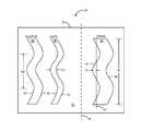
- FIG. 2is a top plan view of an exemplary embodiment of a field effect transistor (FET) having rippled fingers in accordance with the present disclosure.
- FETfield effect transistor
- FIG. 3is a partial plan view of another exemplary embodiment of a FET having rippled fingers in accordance with the present disclosure.
- FIG. 4is a detailed plan view of saw-tooth shaped rippled edges, and semi-circular shaped rippled edges compared to traditional straight edges for traditional transistor fingers.
- FIG. 2is a top plan view of an exemplary embodiment of a field effect transistor (FET) 28 having rippled fingers in accordance with the present disclosure.
- the FET 28includes a semiconductor substrate 30 having a front side 32 with a finger axis 34 .
- a drain finger 36is disposed on the front side 32 of the semiconductor substrate 30 such that the width W of the drain finger 36 lies parallel to the finger axis 34 .
- a gate finger 38is disposed on the front side 32 of the semiconductor substrate 30 and is spaced from the drain finger 36 such that the width W of the gate finger 38 lies parallel to the finger axis 34 .
- a source finger 40is also disposed on the front side 32 of the semiconductor substrate 30 while being spaced from the gate finger 38 such that the width W of the source finger 40 lies parallel to the finger axis 34 .
- the width Wis a greatest dimension for the drain finger 36 , the gate finger 38 , and the source finger 40 , which each have rippled edges 42 that each have ripples with peaks and troughs that are equally disposed about an axis such as axis 43 that is about parallel with the finger axis 34 . While it is to be understood that the rippled edges 42 can have practically any periodic profile, the rippled edges 42 in FIG.
- the wavelength WLis typically a multiple of a minimum GL with the multiple being from around about 1 to around about 10.
- an exemplary wavelength for the rippled edges 42 shown in FIG. 2is approximately 5 to 6 times the gate length GL of the gate finger 38 .
- the amplitude of the rippled edges 42 in FIG. 2is a fraction of the gate length GL of the gate finger 38 .
- the amplitude of the rippled edges 42typically have a fixed amplitude that is a fraction of GL with the fraction being from around about 50% to around about 500%.
- the amplitude of the rippled edges 42is about 1 ⁇ 2 the gate length GL of the gate finger 38 .
- the ripples of the drain finger 36it is advantageous for the ripples of the drain finger 36 to have variable wavelengths, which are in phase with the ripples of the gate finger 38 , which are in phase with the ripples of the source finger 40 .
- the WL for ripples centrally located along axis 43can be less than the WL for ripples at either end of the drain finger 36 .
- At least one advantage for having variable WLis for dissipating a greater heat build-up for the drain finger 36 near ripples centrally located along axis 43 .
- FIG. 3is a partial plan view of another exemplary embodiment of a FET 44 having rippled fingers in accordance with the present disclosure.
- a source finger 46 , a gate finger 48 , and a drain finger 50have rippled edges 52 , which are depicted in dashed lines.
- a lateral spacing (LS GS ) between the source finger 46 and the gate finger 48is constant between the source finger 46 and the gate finger 48 .
- a lateral spacing (LS DG ) between the drain finger 50 and the gate finger 48is constant between the drain finger 50 and the gate finger 48 .
- CS GScritical spacing between the gate finger 48 and the source finger 46 decreases with increasing amplitude of the rippled edges 52 .
- a critical spacing (CS DG ) between the drain finger 50 and the gate finger 48decreases with increasing amplitude of the rippled edges 52 .
- the reduction in the CS GS and the CS DGis evaluated with respect to desired operational voltage of the FET 44 . If it is determined that either the CS GS or the CS DG is too close and may cause a voltage breakdown, an electrical field intensity problem and/or a photolithographic problem, the lateral spacing, either the LS GS and/or the LS DG will be increased to resolve indicated problems. Typically, any increase of the LS GS and/or the LS DG will be relatively slight.
- the FET 44 as depicted in FIG. 3has a wavelength for the rippled edges 52 that is approximately 2 to 3 times the gate length (GL) of the gate finger 48 .
- An exemplary GLis on the order of 1 micron.
- a preferred wavelength range for a 1 micron GLis from around about 0.5 micron to around about 5 microns.
- RDS ONAn on-resistance (RDS ON ) of a lateral FET such as the FET 44 is due to several resistive elements (not shown).
- a source contact resistance and a drain contact resistance, a channel resistance, along with a resistance of a drift region between the gate finger 48 and the drain finger 50make up the RDS ON .
- all of the resistive elementswill be reduced except for the drift region, which remains unaffected by the rippled edges 52 .
- FIG. 4is a detailed plan view of saw-tooth rippled edges 54 having a saw-tooth profile, and semi-circular rippled edges 56 having a profile of peaks and troughs made up of alternating semicircles that replace traditional straight edges 58 for traditional transistor fingers such as a traditional source finger 60 and a traditional gate finger 62 .
- the saw-tooth rippled edges 54each have constant amplitude A ST and a wavelength WL.
- An exemplary A STis equal to 1 ⁇ 2 the gate length GL, while an exemplary WL is equal to 4 times GL.
- the finger width for either of the traditional source finger 60 or the traditional gate finger 62will be increased by around about 41%.
- the CSis reduced by around about 29% in this example. As discussed above, a reduced CS can be mitigated by spacing transistor fingers relatively slightly farther apart.
- Exemplary ones of the semi-circular rippled edges 56are made up of alternating 1 ⁇ 4 circle sections that each have a radius R equal to ( ⁇ 2) ⁇ A C , where A C is the amplitude of the semi-circular rippled edges.
- the WLremains equal to 4 times GL, but the semi-circular rippled edges 56 have an advantage over the saw-tooth rippled edges 54 in that the semi-circular rippled edges 56 have no sharp edges that might increase a susceptibly to voltage breakdown. For instance, if the width W of the traditional gate finger 62 is increased by 11%, the CS will be reduced by 12%.
- the saw-tooth rippled edges 54are better suited for low voltage applications, whereas wavy rippled edges like the semi-circular rippled edges 56 and the sinusoidal like rippled edges 42 ( FIG. 2 ) are better suited for relatively higher voltage applications.
- significant costs reductionsare realized by the present disclosure by providing greater finger width in an area that is smaller than possible using traditional straight edge type transistor fingers for a similar current flow, on-resistance, and breakdown voltage.
Landscapes
- Junction Field-Effect Transistors (AREA)
Abstract
Description
Claims (20)
Priority Applications (1)
| Application Number | Priority Date | Filing Date | Title |
|---|---|---|---|
| US13/966,400US9070761B2 (en) | 2012-08-27 | 2013-08-14 | Field effect transistor (FET) having fingers with rippled edges |
Applications Claiming Priority (3)
| Application Number | Priority Date | Filing Date | Title |
|---|---|---|---|
| US201261693399P | 2012-08-27 | 2012-08-27 | |
| US201361815083P | 2013-04-23 | 2013-04-23 | |
| US13/966,400US9070761B2 (en) | 2012-08-27 | 2013-08-14 | Field effect transistor (FET) having fingers with rippled edges |
Publications (2)
| Publication Number | Publication Date |
|---|---|
| US20140054602A1 US20140054602A1 (en) | 2014-02-27 |
| US9070761B2true US9070761B2 (en) | 2015-06-30 |
Family
ID=50147209
Family Applications (1)
| Application Number | Title | Priority Date | Filing Date |
|---|---|---|---|
| US13/966,400ActiveUS9070761B2 (en) | 2012-08-27 | 2013-08-14 | Field effect transistor (FET) having fingers with rippled edges |
Country Status (1)
| Country | Link |
|---|---|
| US (1) | US9070761B2 (en) |
Cited By (6)
| Publication number | Priority date | Publication date | Assignee | Title |
|---|---|---|---|---|
| US9455327B2 (en) | 2014-06-06 | 2016-09-27 | Qorvo Us, Inc. | Schottky gated transistor with interfacial layer |
| US9536803B2 (en) | 2014-09-05 | 2017-01-03 | Qorvo Us, Inc. | Integrated power module with improved isolation and thermal conductivity |
| US9564497B2 (en) | 2012-04-18 | 2017-02-07 | Qorvo Us, Inc. | High voltage field effect transitor finger terminations |
| US9640632B2 (en) | 2012-08-24 | 2017-05-02 | Qorvo Us, Inc. | Semiconductor device having improved heat dissipation |
| US10062684B2 (en) | 2015-02-04 | 2018-08-28 | Qorvo Us, Inc. | Transition frequency multiplier semiconductor device |
| US10615158B2 (en) | 2015-02-04 | 2020-04-07 | Qorvo Us, Inc. | Transition frequency multiplier semiconductor device |
Families Citing this family (4)
| Publication number | Priority date | Publication date | Assignee | Title |
|---|---|---|---|---|
| US20140021603A1 (en) | 2012-07-23 | 2014-01-23 | Rf Micro Devices, Inc. | Using an interconnect bump to traverse through a passivation layer of a semiconductor die |
| US9202874B2 (en) | 2012-08-24 | 2015-12-01 | Rf Micro Devices, Inc. | Gallium nitride (GaN) device with leakage current-based over-voltage protection |
| US11581215B2 (en)* | 2020-07-14 | 2023-02-14 | Newport Fab, Llc | Body-source-tied semiconductor-on-insulator (SOI) transistor |
| CN114188407B (en)* | 2022-02-17 | 2022-05-06 | 深圳市时代速信科技有限公司 | Semiconductor device electrode structure, manufacturing method and semiconductor device |
Citations (180)
| Publication number | Priority date | Publication date | Assignee | Title |
|---|---|---|---|---|
| US4317055A (en) | 1978-05-24 | 1982-02-23 | Hitachi, Ltd. | High-voltage circuit for insulated gate field-effect transistor |
| US4540954A (en) | 1982-11-24 | 1985-09-10 | Rockwell International Corporation | Singly terminated distributed amplifier |
| US4543535A (en) | 1984-04-16 | 1985-09-24 | Raytheon Company | Distributed power amplifier |
| US4620207A (en) | 1984-12-19 | 1986-10-28 | Eaton Corporation | Edge channel FET |
| US4788511A (en) | 1987-11-30 | 1988-11-29 | Raytheon Company | Distributed power amplifier |
| US5028879A (en) | 1984-05-24 | 1991-07-02 | Texas Instruments Incorporated | Compensation of the gate loading loss for travelling wave power amplifiers |
| US5046155A (en) | 1990-04-06 | 1991-09-03 | Wisconsin Alumni Research Foundation | Highly directive, broadband, bidirectional distributed amplifier |
| US5047355A (en) | 1983-09-21 | 1991-09-10 | Siemens Aktiengesellschaft | Semiconductor diode and method for making it |
| US5107323A (en) | 1988-12-22 | 1992-04-21 | At&T Bell Laboratories | Protective layer for high voltage devices |
| US5118993A (en) | 1990-11-23 | 1992-06-02 | Yang Tai Her | Variable voltage regulator |
| US5208547A (en) | 1991-06-06 | 1993-05-04 | Raytheon Company | Distributed amplifier having negative feedback |
| US5227734A (en) | 1991-08-26 | 1993-07-13 | Raytheon Company | Broadband bipolar transistor distributed amplifier |
| US5306656A (en) | 1988-06-24 | 1994-04-26 | Siliconix Incorporated | Method for reducing on resistance and improving current characteristics of a MOSFET |
| US5361038A (en) | 1993-03-11 | 1994-11-01 | Trw Inc. | Active load applications for distributed circuits |
| US5365197A (en) | 1993-06-30 | 1994-11-15 | Texas Instruments Incorporated | Low-noise distributed amplifier |
| US5389571A (en) | 1991-12-18 | 1995-02-14 | Hiroshi Amano | Method of fabricating a gallium nitride based semiconductor device with an aluminum and nitrogen containing intermediate layer |
| US5414387A (en) | 1993-07-14 | 1995-05-09 | Mitsubishi Denki Kabushiki Kaisha | Distributed amplifier and bidirectional amplifier |
| US5485118A (en) | 1994-06-03 | 1996-01-16 | Massachusetts Institute Of Technology | Non-uniformly distributed power amplifier |
| US5608353A (en) | 1995-03-29 | 1997-03-04 | Rf Micro Devices, Inc. | HBT power amplifier |
| US5698870A (en) | 1996-07-22 | 1997-12-16 | The United States Of America As Represented By The Secretary Of The Air Force | High electron mobility transistor (HEMT) and pseudomorphic high electron mobility transistor (PHEMT) devices with single layer integrated metal |
| US5742205A (en) | 1995-07-27 | 1998-04-21 | Scientific-Atlanta, Inc. | Field effect transistor cable television line amplifier |
| US5764673A (en) | 1995-09-25 | 1998-06-09 | Mitsubishi Denki Kabushiki Kaisha | Semiconductor light emitting device |
| JPH10242584A (en) | 1997-02-28 | 1998-09-11 | Hitachi Ltd | Semiconductor light emitting device |
| US5834326A (en) | 1995-12-12 | 1998-11-10 | Pioneer Electronic Corporation | Process for producing a luminous element of group III nitride semi-conductor |
| US5843590A (en) | 1994-12-26 | 1998-12-01 | Sumitomo Electric Industries, Ltd. | Epitaxial wafer and method of preparing the same |
| US5864156A (en) | 1995-12-15 | 1999-01-26 | Micron Technology, Inc. | Isolated plugged contacts |
| US5874747A (en) | 1996-02-05 | 1999-02-23 | Advanced Technology Materials, Inc. | High brightness electroluminescent device emitting in the green to ultraviolet spectrum and method of making the same |
| US5880640A (en) | 1989-11-24 | 1999-03-09 | Dassault Electronique | Distributed amplifier for wide band hyperfrequency signals |
| US5914501A (en) | 1998-08-27 | 1999-06-22 | Hewlett-Packard Company | Light emitting diode assembly having integrated electrostatic discharge protection |
| US5949140A (en) | 1996-05-30 | 1999-09-07 | Oki Electric Industry Co., Ltd. | Microwave semiconductor device with via holes and associated structure |
| JP2000031535A (en) | 1998-07-10 | 2000-01-28 | Murata Mfg Co Ltd | Semiconductor light emitting element |
| US6049250A (en) | 1998-04-03 | 2000-04-11 | Trw Inc. | Dittributed feed back distributed amplifier |
| US6064082A (en) | 1997-05-30 | 2000-05-16 | Sony Corporation | Heterojunction field effect transistor |
| US6110757A (en) | 1996-08-07 | 2000-08-29 | Showa Denko K. K. | Method of forming epitaxial wafer for light-emitting device including an active layer having a two-phase structure |
| US6130579A (en) | 1999-03-29 | 2000-10-10 | Rf Micro Devices, Inc. | Feed-forward biasing for RF amplifiers |
| US6133589A (en) | 1999-06-08 | 2000-10-17 | Lumileds Lighting, U.S., Llc | AlGaInN-based LED having thick epitaxial layer for improved light extraction |
| US6177685B1 (en) | 1998-01-20 | 2001-01-23 | Sharp Kabushiki Kaisha | Nitride-type III-V HEMT having an InN 2DEG channel layer |
| US6191656B1 (en) | 1999-07-23 | 2001-02-20 | Rf Micro Devices, Inc. | High efficiency, unilateral dual stage RF amplifier |
| US6229395B1 (en) | 1999-10-01 | 2001-05-08 | Rf Micro Devices, Inc. | Differential transconductance amplifier |
| US6265943B1 (en) | 2000-01-27 | 2001-07-24 | Rf Micro Devices, Inc. | Integrated RF power sensor that compensates for bias changes |
| US6271727B1 (en) | 1999-08-06 | 2001-08-07 | Rf Micro Devices, Inc. | High isolation RF power amplifier with self-bias attenuator |
| US6307364B1 (en) | 1999-08-27 | 2001-10-23 | Rf Micro Devices, Inc. | Power sensor for RF power amplifier |
| US6306709B1 (en) | 1994-06-03 | 2001-10-23 | Seiko Instruments Inc. | Semiconductor device and manufacturing method thereof |
| US6313705B1 (en) | 1999-12-20 | 2001-11-06 | Rf Micro Devices, Inc. | Bias network for high efficiency RF linear power amplifier |
| US20010040246A1 (en) | 2000-02-18 | 2001-11-15 | Hirotatsu Ishii | GaN field-effect transistor and method of manufacturing the same |
| US6329809B1 (en) | 1999-08-27 | 2001-12-11 | Rf Micro Devices, Inc. | RF power amplifier output power sensor |
| US6333677B1 (en) | 2000-10-10 | 2001-12-25 | Rf Micro Devices, Inc. | Linear power amplifier bias circuit |
| US20010054848A1 (en) | 1999-02-08 | 2001-12-27 | Siemens Ag. | Method and apparatus for balancing the power losses in a number of parallel-connected cascode circuits |
| US6342815B1 (en) | 2000-10-04 | 2002-01-29 | Trw Inc. | Manufacturable HBT power distributed amplifier for wideband telecommunications |
| US6356150B1 (en) | 2000-01-21 | 2002-03-12 | Rf Micro Devices, Inc. | Portable integrated switching power amplifier |
| EP1187229A1 (en) | 2000-02-21 | 2002-03-13 | Sanken Electric Co., Ltd. | Light-emitting semiconductor device and method of manufacture thereof |
| US20020031851A1 (en) | 1998-11-24 | 2002-03-14 | Linthicum Kevin J. | Methods of fabricating gallium nitride microelectronic layers on silicon layers and gallium nitride microelectronic structures formed thereby |
| US6373318B1 (en) | 1998-09-25 | 2002-04-16 | Siemens Aktiengesellschaft | Electronic switching device having at least two semiconductor components |
| US6376864B1 (en) | 1999-07-06 | 2002-04-23 | Tien Yang Wang | Semiconductor light-emitting device and method for manufacturing the same |
| US6377125B1 (en) | 2001-03-15 | 2002-04-23 | Motorola.Inc. | Distributed amplifier having separately biased sections |
| US20020048302A1 (en) | 1997-06-19 | 2002-04-25 | Akitaka Kimura | Gallium nitride semiconductor laser and a manufacturing process thereof |
| US6384433B1 (en) | 2000-03-23 | 2002-05-07 | Rf Micro Devices, Inc. | Voltage variable resistor from HBT epitaxial layers |
| US6387733B1 (en) | 2001-05-22 | 2002-05-14 | Rf Micro Devices, Inc. | Time-based semiconductor material attachment |
| US6392487B1 (en) | 2000-08-02 | 2002-05-21 | Rf Micro Devices, Inc | Variable gain amplifier |
| US6400226B2 (en) | 1999-12-02 | 2002-06-04 | Fujitsu Limited | Distributed amplifier with improved flatness of frequency characteristic |
| US20020079508A1 (en)* | 2000-12-19 | 2002-06-27 | The Furukawa Electric Co., Ltd. | GaN-based high electron mobility transistor |
| US6448793B1 (en) | 2000-04-07 | 2002-09-10 | Rf Micro Devices, Inc. | Adaptive manufacturing of semiconductor circuits |
| US6455877B1 (en) | 1999-09-08 | 2002-09-24 | Sharp Kabushiki Kaisha | III-N compound semiconductor device |
| US6477682B2 (en) | 1998-09-24 | 2002-11-05 | Sun Microsystems, Inc. | Technique for partitioning data to correct memory part failures |
| US6475916B1 (en) | 2000-01-18 | 2002-11-05 | Chartered Semiconductor Manufacturing Ltd. | Method of patterning gate electrode with ultra-thin gate dielectric |
| US20030003630A1 (en) | 2001-06-28 | 2003-01-02 | Junichi Iimura | Hybrid integrated circuit device |
| US6521998B1 (en) | 1998-12-28 | 2003-02-18 | Sharp Kabushiki Kaisha | Electrode structure for nitride III-V compound semiconductor devices |
| US6525611B1 (en) | 2001-08-01 | 2003-02-25 | Rf Micro Devices, Inc. | Power amplifier protection |
| US6560452B1 (en) | 2000-11-27 | 2003-05-06 | Rf Micro Devices, Inc. | Oscillator having a transistor formed of a wide bandgap semiconductor material |
| US6566963B1 (en) | 2002-02-07 | 2003-05-20 | Rf Micro Devices, Inc. | Transformer-based low noise variable gain driver amplifier |
| US20030122139A1 (en) | 2001-12-28 | 2003-07-03 | United Epitaxy Co., Ltd. | Light emitting diode package structure having an electro-static protective diode |
| US6589877B1 (en) | 1998-02-02 | 2003-07-08 | Micron Technology, Inc. | Method of providing an oxide |
| US6593597B2 (en) | 2001-06-05 | 2003-07-15 | South Epitaxy Corporation | Group III-V element-based LED having ESD protection capacity |
| US6608367B1 (en) | 2002-02-25 | 2003-08-19 | Rf Micro Devices, Inc. | Leadframe inductors |
| US20030160317A1 (en) | 2000-01-31 | 2003-08-28 | Noriaki Sakamoto | Circuit device and manufacturing method of circuit device and semiconductor module |
| US6614281B1 (en) | 1999-06-11 | 2003-09-02 | Siemens Aktiengesellschaft | Method and device for disconnecting a cascode circuit with voltage-controlled semiconductor switches |
| US6624452B2 (en) | 2000-07-28 | 2003-09-23 | The Regents Of The University Of California | Gallium nitride-based HFET and a method for fabricating a gallium nitride-based HFET |
| US6627552B1 (en) | 2000-03-29 | 2003-09-30 | Kabsuhiki Kaisha Toshiba | Method for preparing epitaxial-substrate and method for manufacturing semiconductor device employing the same |
| US6633073B2 (en) | 2001-06-29 | 2003-10-14 | Rf Micro Devices, Inc. | Method and apparatus for isolating circuits using deep substrate n-well |
| US6633195B2 (en) | 1999-01-22 | 2003-10-14 | Siemens Aktiengesellschaft | Hybrid power MOSFET |
| US6639470B1 (en) | 2000-10-06 | 2003-10-28 | Skyworks Solutions, Inc. | Constant current biasing circuit for linear power amplifiers |
| US20030206440A1 (en) | 2002-05-06 | 2003-11-06 | Wong Sau Ching | Bi-directional floating gate nonvolatile memory |
| JP2003332618A (en) | 2002-05-10 | 2003-11-21 | Mitsubishi Cable Ind Ltd | Semiconductor light emitting element |
| US20030218183A1 (en) | 2001-12-06 | 2003-11-27 | Miroslav Micovic | High power-low noise microwave GaN heterojunction field effet transistor |
| US6657592B2 (en) | 2002-04-26 | 2003-12-02 | Rf Micro Devices, Inc. | Patch antenna |
| US6656271B2 (en) | 1998-12-04 | 2003-12-02 | Canon Kabushiki Kaisha | Method of manufacturing semiconductor wafer method of using and utilizing the same |
| US6660606B2 (en) | 2000-09-29 | 2003-12-09 | Canon Kabushiki Kaisha | Semiconductor-on-insulator annealing method |
| US6701134B1 (en) | 2002-11-05 | 2004-03-02 | Rf Micro Devices, Inc. | Increased dynamic range for power amplifiers used with polar modulation |
| US6701138B2 (en) | 2001-06-11 | 2004-03-02 | Rf Micro Devices, Inc. | Power amplifier control |
| US6706576B1 (en) | 2002-03-14 | 2004-03-16 | Advanced Micro Devices, Inc. | Laser thermal annealing of silicon nitride for increased density and etch selectivity |
| US6720831B2 (en) | 2002-04-26 | 2004-04-13 | Rf Micro Devices, Inc. | Power amplifier protection circuit |
| US20040070003A1 (en) | 2002-10-09 | 2004-04-15 | Remigijus Gaska | Semiconductor structure having a textured nitride-based layer |
| US6724252B2 (en) | 2002-02-21 | 2004-04-20 | Rf Micro Devices, Inc. | Switched gain amplifier circuit |
| US6723587B2 (en) | 2002-09-19 | 2004-04-20 | Electronics And Telecommunications Research Institute | Ultra small-sized SOI MOSFET and method of fabricating the same |
| US6727762B1 (en) | 2002-11-26 | 2004-04-27 | Sirenza Microdevices, Inc. | Direct coupled distributed amplifier |
| US6748204B1 (en) | 2000-10-17 | 2004-06-08 | Rf Micro Devices, Inc. | Mixer noise reduction technique |
| US6750158B2 (en) | 2001-05-18 | 2004-06-15 | Matsushita Electric Industrial Co., Ltd. | Method for producing a semiconductor device |
| US6750482B2 (en) | 2002-04-30 | 2004-06-15 | Rf Micro Devices, Inc. | Highly conductive semiconductor layer having two or more impurities |
| US6759907B2 (en) | 2002-01-25 | 2004-07-06 | Centellax, Inc. | Distributed level-shifting network for cascading broadband amplifiers |
| US20040130037A1 (en) | 2003-01-02 | 2004-07-08 | Cree Lighting Company | Group III nitride based flip-chip intergrated circuit and method for fabricating |
| US6802902B2 (en) | 1997-10-20 | 2004-10-12 | Lumilog | Process for producing an epitaxial layer of gallium nitride |
| US6815722B2 (en) | 2002-12-13 | 2004-11-09 | Vetra Technology, Inc. | Light-emitting device with reduced lattice mismatch |
| US6815730B2 (en) | 2001-01-31 | 2004-11-09 | Sharp Kabushiki Kaisha | Nitride-based semiconductor light-emitting device |
| US6822842B2 (en) | 2001-07-23 | 2004-11-23 | Siced Electronics Development Gmbh & Co. Kg | Switching device for switching at a high operating voltage |
| US20040241916A1 (en) | 2002-08-23 | 2004-12-02 | Chau Robert S. | Tri-gate devices and methods of fabrication |
| WO2004051707A3 (en) | 2002-12-04 | 2005-02-17 | Emcore Corp | Gallium nitride-based devices and manufacturing process |
| US6861677B2 (en) | 2002-03-04 | 2005-03-01 | United Epitaxy Co., Ltd. | Package of lightemitting diode with protective element |
| US20050139868A1 (en) | 2003-12-24 | 2005-06-30 | Matsushita Electric Industrial Co., Ltd. | Field effect transistor and method of manufacturing the same |
| US20050189559A1 (en) | 2004-02-27 | 2005-09-01 | Kabushiki Kaisha Toshiba | Semiconductor device |
| US20050189562A1 (en) | 2004-02-12 | 2005-09-01 | Kinzer Daniel M. | Integrated III-nitride power devices |
| US20050194612A1 (en) | 2004-01-23 | 2005-09-08 | International Rectifier Corp. | III-Nitride current control device and method of manufacture |
| US6943631B2 (en) | 2003-12-23 | 2005-09-13 | Agilent Technologies, Inc. | DC-coupled multi-stage amplifier using all-pass resistive/capacitive network for level shifting |
| US20050212049A1 (en) | 2004-03-24 | 2005-09-29 | Koji Onodera | Semiconductor device and process for producing the same |
| US20050225912A1 (en) | 2004-04-12 | 2005-10-13 | Sandeep Pant | Electrical over stress robustness |
| US20050271107A1 (en) | 2004-06-08 | 2005-12-08 | Fuji Xerox Co., Ltd. | Semiconductor laser apparatus and manufacturing method thereof |
| US20060043385A1 (en) | 2004-08-27 | 2006-03-02 | Institute Of Semiconductors, Chinese Academy Of Sciences | White light emitting diode of a blue and yellow light emitting (structure) layer stacked structure and method of manufacturing the same |
| US7015512B2 (en) | 2003-12-20 | 2006-03-21 | Samsung Electro-Mechanics Co., Ltd. | High power flip chip LED |
| US20060068601A1 (en) | 2004-09-29 | 2006-03-30 | Jeong-Sik Lee | Wafer for compound semiconductor devices, and method of fabrication |
| US7026665B1 (en) | 2003-09-19 | 2006-04-11 | Rf Micro Devices, Inc. | High voltage GaN-based transistor structure |
| US7033961B1 (en) | 2003-07-15 | 2006-04-25 | Rf Micro Devices, Inc. | Epitaxy/substrate release layer |
| US7042150B2 (en) | 2002-12-20 | 2006-05-09 | Showa Denko K.K. | Light-emitting device, method of fabricating the device, and LED lamp using the device |
| US7052942B1 (en) | 2003-09-19 | 2006-05-30 | Rf Micro Devices, Inc. | Surface passivation of GaN devices in epitaxial growth chamber |
| US20060124960A1 (en) | 2004-12-13 | 2006-06-15 | Matsushita Electric Industrial Co., Ltd. | Semiconductor device and method for fabricating the same |
| US20060243988A1 (en) | 2005-05-02 | 2006-11-02 | Nichia Corporation | Nitride semiconductor element |
| US20070093009A1 (en) | 2000-05-26 | 2007-04-26 | Commissariat A L'energie Atomique | Semiconductor device with vertical electron injection and its manufacturing method |
| US7211822B2 (en) | 1997-01-09 | 2007-05-01 | Nichia Chemical Industries, Ltd. | Nitride semiconductor device |
| KR20070066051A (en) | 2005-12-21 | 2007-06-27 | 엘지노텔 주식회사 | Analysis method of power supply circuit noise using 2 terminal network theory |
| EP1826041A1 (en) | 2006-02-28 | 2007-08-29 | Dometic Corporation | Variable speed control |
| US20070295985A1 (en) | 2001-02-23 | 2007-12-27 | Nitronex Corporation | Gallium nitride material devices and methods of forming the same |
| US20080023706A1 (en) | 2006-07-26 | 2008-01-31 | Kabushiki Kaisha Toshiba | Nitride semiconductor device |
| US20080073752A1 (en) | 2006-09-27 | 2008-03-27 | Nec Electronics Corporation | Semiconductor apparatus |
| US20080112448A1 (en) | 2006-11-09 | 2008-05-15 | Tetsuzo Ueda | Nitride semiconductor laser diode |
| US20080121875A1 (en) | 2006-11-24 | 2008-05-29 | Lg.Philips Lcd Co., Ltd. | Array substrate for liquid crystal display device and method of fabricating the same |
| US20080142837A1 (en) | 2006-11-09 | 2008-06-19 | The Furukawa Electric Co., Ltd. | Vertical type semiconductor device and manufacturing method of the device |
| JP2008148511A (en) | 2006-12-13 | 2008-06-26 | Matsushita Electric Ind Co Ltd | Inverter circuit |
| US20080179737A1 (en) | 2006-10-03 | 2008-07-31 | Rohm Co., Ltd. | Semiconductor device |
| US20080190355A1 (en) | 2004-07-07 | 2008-08-14 | Ii-Vi Incorporated | Low-Doped Semi-Insulating Sic Crystals and Method |
| JP2008258419A (en) | 2007-04-05 | 2008-10-23 | Toshiba Corp | Nitride semiconductor device |
| US20080272422A1 (en) | 2007-05-03 | 2008-11-06 | Dsm Solutions, Inc. | Transistor Providing Different Threshold Voltages and Method of Fabrication Thereof |
| US20080272382A1 (en) | 2006-03-07 | 2008-11-06 | Lg Electronics Inc. | Light emitting device and method of manufacturing the same |
| US7449762B1 (en) | 2006-04-07 | 2008-11-11 | Wide Bandgap Llc | Lateral epitaxial GaN metal insulator semiconductor field effect transistor |
| US20080283821A1 (en) | 2007-05-17 | 2008-11-20 | Samsung Corning Co., Ltd. | Method of growing gan crystal on silicon substrate, and light emitting device and method of manufacturing thereof |
| US20080308813A1 (en) | 2006-08-18 | 2008-12-18 | Chang Soo Suh | High breakdown enhancement mode gallium nitride based high electron mobility transistors with integrated slant field plate |
| US20090072269A1 (en) | 2007-09-17 | 2009-03-19 | Chang Soo Suh | Gallium nitride diodes and integrated components |
| US20090146185A1 (en) | 2007-12-10 | 2009-06-11 | Transphorm Inc. | Insulated gate e-mode transistors |
| US20090146186A1 (en) | 2007-12-07 | 2009-06-11 | The Government of the United State of America, as represented by the Secretary of the Navy | Gate after Diamond Transistor |
| US20090166677A1 (en) | 2007-12-28 | 2009-07-02 | Daisuke Shibata | Semiconductor device and manufacturing method thereof |
| US7557421B1 (en) | 2006-07-20 | 2009-07-07 | Rf Micro Devices, Inc. | Hybrid radio frequency integrated circuit using gallium nitride epitaxy layers grown on a donor substrate |
| US20090278137A1 (en) | 2008-05-08 | 2009-11-12 | Semisouth Laboratories, Inc. | Semiconductor devices with non-punch-through semiconductor channels having enhanced conduction and methods of making |
| US7719055B1 (en) | 2007-05-10 | 2010-05-18 | Northrop Grumman Systems Corporation | Cascode power switch topologies |
| US20100133567A1 (en) | 2007-05-21 | 2010-06-03 | Lg Innotek Co., Ltd | Semiconductor light emitting device and method of manufacturing the same |
| US20100187575A1 (en) | 2009-01-28 | 2010-07-29 | Peter Baumgartner | Semiconductor Element and a Method for Producing the Same |
| US7768758B2 (en) | 2004-09-27 | 2010-08-03 | Siemens Aktiengesellschaft | Electronic switching device, in particular circuit-breaker and associated operating method |
| US20100207164A1 (en) | 2008-08-22 | 2010-08-19 | Daisuke Shibata | Field effect transistor |
| US20100230656A1 (en) | 2009-02-16 | 2010-09-16 | Rfmd (Uk) Limited | Light emitting structure and method of manufacture thereof |
| US20100230717A1 (en) | 2009-03-13 | 2010-09-16 | Kabushiki Kaisha Toshiba | Semiconductor device |
| US7804262B2 (en) | 2006-05-15 | 2010-09-28 | Carrier Corporation | Non-intrusive electronic control circuitry to detect an open protector in a hermetically sealed compressor |
| US20100258898A1 (en) | 2007-11-27 | 2010-10-14 | S.O.I Tec Silicon On Insulator Technologies | Process for fabricating an electronic device |
| US20110017972A1 (en) | 2009-07-22 | 2011-01-27 | Rfmd (Uk) Limited | Light emitting structure with integral reverse voltage protection |
| US20110025422A1 (en) | 2009-07-30 | 2011-02-03 | Qualcomm Incorporated | Power amplifier bias current monitor and control mechanism |
| US20110095337A1 (en) | 2009-10-22 | 2011-04-28 | Ken Sato | Semiconductor device and method of manufacturing the same |
| US20110115025A1 (en) | 2009-11-17 | 2011-05-19 | Fujitsu Limited | Semiconductor device and method of manufacturing semiconductor device |
| US20110127586A1 (en) | 2009-11-30 | 2011-06-02 | Madhur Bobde | Lateral super junction device with high substrate-gate breakdown and built-in avalanche clamp diode |
| US20110163342A1 (en) | 2007-07-23 | 2011-07-07 | Kyung Jun Kim | Light emitting device |
| US20110175142A1 (en) | 2008-10-22 | 2011-07-21 | Panasonic Corporation | Nitride semiconductor device |
| US20110199148A1 (en) | 2010-02-15 | 2011-08-18 | Denso Corporation | Hybrid power device |
| US20110211289A1 (en) | 2010-02-26 | 2011-09-01 | Lex Kosowsky | Embedded protection against spurious electrical events |
| US8017981B2 (en) | 2004-07-08 | 2011-09-13 | Semisouth Laboratories, Inc. | Normally-off integrated JFET power switches in wide bandgap semiconductors and methods of making |
| US20110242921A1 (en) | 2010-03-30 | 2011-10-06 | Hieu Van Tran | Systems And Methods Of Non-Volatile Memory Sensing Including Selective/Differential Threshold Voltage Features |
| US20110290174A1 (en) | 2002-06-24 | 2011-12-01 | Navy, Secretary Of The, United States Of America | One hundred millimeter single crystal silicon carbide wafer |
| WO2011162243A1 (en) | 2010-06-24 | 2011-12-29 | ザ ユニバーシティ オブ シェフィールド | Semiconductor device |
| US20120018735A1 (en) | 2010-07-20 | 2012-01-26 | Sumitomo Electric Device Innovations, Inc. | Semiconductor device |
| US20120126240A1 (en) | 2010-11-19 | 2012-05-24 | Electronics And Telecommunications Research Institute | Wafer level packaged GaN power device and the manufacturing method thereof |
| US20120199875A1 (en) | 2011-02-03 | 2012-08-09 | Anup Bhalla | Cascode scheme for improved device switching behavior |
| US20120211802A1 (en)* | 2011-02-23 | 2012-08-23 | Sony Corporation | Field effect transistor, semiconductor switch circuit, and communication apparatus |
| US20120218783A1 (en) | 2011-02-25 | 2012-08-30 | Fujitsu Limited | Compound semiconductor device and method for manufacturing the same |
| US20120262220A1 (en) | 2011-04-13 | 2012-10-18 | Semisouth Laboratories, Inc. | Cascode switches including normally-off and normally-on devices and circuits comprising the switches |
| US20130280877A1 (en) | 2012-04-18 | 2013-10-24 | Rf Micro Devices, Inc. | Methods for fabricating high voltage field effect transitor finger terminations |
| US8633518B2 (en) | 2007-09-17 | 2014-01-21 | Transphorm Inc. | Gallium nitride power devices |
| US8692294B2 (en) | 2009-08-28 | 2014-04-08 | Transphorm Inc. | Semiconductor devices with field plates |
- 2013
- 2013-08-14USUS13/966,400patent/US9070761B2/enactiveActive
Patent Citations (200)
| Publication number | Priority date | Publication date | Assignee | Title |
|---|---|---|---|---|
| US4317055A (en) | 1978-05-24 | 1982-02-23 | Hitachi, Ltd. | High-voltage circuit for insulated gate field-effect transistor |
| US4540954A (en) | 1982-11-24 | 1985-09-10 | Rockwell International Corporation | Singly terminated distributed amplifier |
| US5047355A (en) | 1983-09-21 | 1991-09-10 | Siemens Aktiengesellschaft | Semiconductor diode and method for making it |
| US4543535A (en) | 1984-04-16 | 1985-09-24 | Raytheon Company | Distributed power amplifier |
| US5028879A (en) | 1984-05-24 | 1991-07-02 | Texas Instruments Incorporated | Compensation of the gate loading loss for travelling wave power amplifiers |
| US4620207A (en) | 1984-12-19 | 1986-10-28 | Eaton Corporation | Edge channel FET |
| US4788511A (en) | 1987-11-30 | 1988-11-29 | Raytheon Company | Distributed power amplifier |
| US5306656A (en) | 1988-06-24 | 1994-04-26 | Siliconix Incorporated | Method for reducing on resistance and improving current characteristics of a MOSFET |
| US5107323A (en) | 1988-12-22 | 1992-04-21 | At&T Bell Laboratories | Protective layer for high voltage devices |
| US5880640A (en) | 1989-11-24 | 1999-03-09 | Dassault Electronique | Distributed amplifier for wide band hyperfrequency signals |
| US5046155A (en) | 1990-04-06 | 1991-09-03 | Wisconsin Alumni Research Foundation | Highly directive, broadband, bidirectional distributed amplifier |
| US5118993A (en) | 1990-11-23 | 1992-06-02 | Yang Tai Her | Variable voltage regulator |
| US5208547A (en) | 1991-06-06 | 1993-05-04 | Raytheon Company | Distributed amplifier having negative feedback |
| US5227734A (en) | 1991-08-26 | 1993-07-13 | Raytheon Company | Broadband bipolar transistor distributed amplifier |
| US5389571A (en) | 1991-12-18 | 1995-02-14 | Hiroshi Amano | Method of fabricating a gallium nitride based semiconductor device with an aluminum and nitrogen containing intermediate layer |
| US5361038A (en) | 1993-03-11 | 1994-11-01 | Trw Inc. | Active load applications for distributed circuits |
| US5365197A (en) | 1993-06-30 | 1994-11-15 | Texas Instruments Incorporated | Low-noise distributed amplifier |
| US5414387A (en) | 1993-07-14 | 1995-05-09 | Mitsubishi Denki Kabushiki Kaisha | Distributed amplifier and bidirectional amplifier |
| US5485118A (en) | 1994-06-03 | 1996-01-16 | Massachusetts Institute Of Technology | Non-uniformly distributed power amplifier |
| US6306709B1 (en) | 1994-06-03 | 2001-10-23 | Seiko Instruments Inc. | Semiconductor device and manufacturing method thereof |
| US5843590A (en) | 1994-12-26 | 1998-12-01 | Sumitomo Electric Industries, Ltd. | Epitaxial wafer and method of preparing the same |
| US5608353A (en) | 1995-03-29 | 1997-03-04 | Rf Micro Devices, Inc. | HBT power amplifier |
| US5629648A (en) | 1995-03-29 | 1997-05-13 | Rf Micro Devices, Inc. | HBT power amplifier |
| US5742205A (en) | 1995-07-27 | 1998-04-21 | Scientific-Atlanta, Inc. | Field effect transistor cable television line amplifier |
| US5764673A (en) | 1995-09-25 | 1998-06-09 | Mitsubishi Denki Kabushiki Kaisha | Semiconductor light emitting device |
| US5834326A (en) | 1995-12-12 | 1998-11-10 | Pioneer Electronic Corporation | Process for producing a luminous element of group III nitride semi-conductor |
| US5864156A (en) | 1995-12-15 | 1999-01-26 | Micron Technology, Inc. | Isolated plugged contacts |
| US5874747A (en) | 1996-02-05 | 1999-02-23 | Advanced Technology Materials, Inc. | High brightness electroluminescent device emitting in the green to ultraviolet spectrum and method of making the same |
| US5949140A (en) | 1996-05-30 | 1999-09-07 | Oki Electric Industry Co., Ltd. | Microwave semiconductor device with via holes and associated structure |
| US5698870A (en) | 1996-07-22 | 1997-12-16 | The United States Of America As Represented By The Secretary Of The Air Force | High electron mobility transistor (HEMT) and pseudomorphic high electron mobility transistor (PHEMT) devices with single layer integrated metal |
| US6110757A (en) | 1996-08-07 | 2000-08-29 | Showa Denko K. K. | Method of forming epitaxial wafer for light-emitting device including an active layer having a two-phase structure |
| US20100025657A1 (en) | 1997-01-09 | 2010-02-04 | Shinichi Nagahama | Nitride semiconductor device |
| US7211822B2 (en) | 1997-01-09 | 2007-05-01 | Nichia Chemical Industries, Ltd. | Nitride semiconductor device |
| JPH10242584A (en) | 1997-02-28 | 1998-09-11 | Hitachi Ltd | Semiconductor light emitting device |
| US6064082A (en) | 1997-05-30 | 2000-05-16 | Sony Corporation | Heterojunction field effect transistor |
| US20020048302A1 (en) | 1997-06-19 | 2002-04-25 | Akitaka Kimura | Gallium nitride semiconductor laser and a manufacturing process thereof |
| US6802902B2 (en) | 1997-10-20 | 2004-10-12 | Lumilog | Process for producing an epitaxial layer of gallium nitride |
| US6177685B1 (en) | 1998-01-20 | 2001-01-23 | Sharp Kabushiki Kaisha | Nitride-type III-V HEMT having an InN 2DEG channel layer |
| US6589877B1 (en) | 1998-02-02 | 2003-07-08 | Micron Technology, Inc. | Method of providing an oxide |
| US6049250A (en) | 1998-04-03 | 2000-04-11 | Trw Inc. | Dittributed feed back distributed amplifier |
| JP2000031535A (en) | 1998-07-10 | 2000-01-28 | Murata Mfg Co Ltd | Semiconductor light emitting element |
| US5914501A (en) | 1998-08-27 | 1999-06-22 | Hewlett-Packard Company | Light emitting diode assembly having integrated electrostatic discharge protection |
| US6477682B2 (en) | 1998-09-24 | 2002-11-05 | Sun Microsystems, Inc. | Technique for partitioning data to correct memory part failures |
| US6373318B1 (en) | 1998-09-25 | 2002-04-16 | Siemens Aktiengesellschaft | Electronic switching device having at least two semiconductor components |
| US20020031851A1 (en) | 1998-11-24 | 2002-03-14 | Linthicum Kevin J. | Methods of fabricating gallium nitride microelectronic layers on silicon layers and gallium nitride microelectronic structures formed thereby |
| US6656271B2 (en) | 1998-12-04 | 2003-12-02 | Canon Kabushiki Kaisha | Method of manufacturing semiconductor wafer method of using and utilizing the same |
| US6521998B1 (en) | 1998-12-28 | 2003-02-18 | Sharp Kabushiki Kaisha | Electrode structure for nitride III-V compound semiconductor devices |
| US6633195B2 (en) | 1999-01-22 | 2003-10-14 | Siemens Aktiengesellschaft | Hybrid power MOSFET |
| US20010054848A1 (en) | 1999-02-08 | 2001-12-27 | Siemens Ag. | Method and apparatus for balancing the power losses in a number of parallel-connected cascode circuits |
| US6285239B1 (en) | 1999-03-29 | 2001-09-04 | Rf Micro Devices, Inc. | Feed-forward biasing for RF amplifiers |
| US6130579A (en) | 1999-03-29 | 2000-10-10 | Rf Micro Devices, Inc. | Feed-forward biasing for RF amplifiers |
| US6133589A (en) | 1999-06-08 | 2000-10-17 | Lumileds Lighting, U.S., Llc | AlGaInN-based LED having thick epitaxial layer for improved light extraction |
| US6614281B1 (en) | 1999-06-11 | 2003-09-02 | Siemens Aktiengesellschaft | Method and device for disconnecting a cascode circuit with voltage-controlled semiconductor switches |
| US6376864B1 (en) | 1999-07-06 | 2002-04-23 | Tien Yang Wang | Semiconductor light-emitting device and method for manufacturing the same |
| US6191656B1 (en) | 1999-07-23 | 2001-02-20 | Rf Micro Devices, Inc. | High efficiency, unilateral dual stage RF amplifier |
| US6271727B1 (en) | 1999-08-06 | 2001-08-07 | Rf Micro Devices, Inc. | High isolation RF power amplifier with self-bias attenuator |
| US6528983B1 (en) | 1999-08-27 | 2003-03-04 | Rf Micro Devices, Inc. | Power sensor for RF power amplifier |
| US6307364B1 (en) | 1999-08-27 | 2001-10-23 | Rf Micro Devices, Inc. | Power sensor for RF power amplifier |
| US6329809B1 (en) | 1999-08-27 | 2001-12-11 | Rf Micro Devices, Inc. | RF power amplifier output power sensor |
| US6455877B1 (en) | 1999-09-08 | 2002-09-24 | Sharp Kabushiki Kaisha | III-N compound semiconductor device |
| US6229395B1 (en) | 1999-10-01 | 2001-05-08 | Rf Micro Devices, Inc. | Differential transconductance amplifier |
| US6400226B2 (en) | 1999-12-02 | 2002-06-04 | Fujitsu Limited | Distributed amplifier with improved flatness of frequency characteristic |
| US6369656B2 (en) | 1999-12-20 | 2002-04-09 | Rf Micro Devices, Inc. | Bias network for high efficiency RF linear power amplifier |
| US6313705B1 (en) | 1999-12-20 | 2001-11-06 | Rf Micro Devices, Inc. | Bias network for high efficiency RF linear power amplifier |
| US6369657B2 (en) | 1999-12-20 | 2002-04-09 | Rf Micro Devices, Inc. | Bias network for high efficiency RF linear power amplifier |
| US6404287B2 (en) | 1999-12-20 | 2002-06-11 | Rf Micro Devices, Inc. | Bias network for high efficiency RF linear power amplifier |
| US6475916B1 (en) | 2000-01-18 | 2002-11-05 | Chartered Semiconductor Manufacturing Ltd. | Method of patterning gate electrode with ultra-thin gate dielectric |
| US6356150B1 (en) | 2000-01-21 | 2002-03-12 | Rf Micro Devices, Inc. | Portable integrated switching power amplifier |
| US6265943B1 (en) | 2000-01-27 | 2001-07-24 | Rf Micro Devices, Inc. | Integrated RF power sensor that compensates for bias changes |
| US20030160317A1 (en) | 2000-01-31 | 2003-08-28 | Noriaki Sakamoto | Circuit device and manufacturing method of circuit device and semiconductor module |
| US20010040246A1 (en) | 2000-02-18 | 2001-11-15 | Hirotatsu Ishii | GaN field-effect transistor and method of manufacturing the same |
| EP1187229A1 (en) | 2000-02-21 | 2002-03-13 | Sanken Electric Co., Ltd. | Light-emitting semiconductor device and method of manufacture thereof |
| US6384433B1 (en) | 2000-03-23 | 2002-05-07 | Rf Micro Devices, Inc. | Voltage variable resistor from HBT epitaxial layers |
| US6627552B1 (en) | 2000-03-29 | 2003-09-30 | Kabsuhiki Kaisha Toshiba | Method for preparing epitaxial-substrate and method for manufacturing semiconductor device employing the same |
| US6448793B1 (en) | 2000-04-07 | 2002-09-10 | Rf Micro Devices, Inc. | Adaptive manufacturing of semiconductor circuits |
| US20070093009A1 (en) | 2000-05-26 | 2007-04-26 | Commissariat A L'energie Atomique | Semiconductor device with vertical electron injection and its manufacturing method |
| US6624452B2 (en) | 2000-07-28 | 2003-09-23 | The Regents Of The University Of California | Gallium nitride-based HFET and a method for fabricating a gallium nitride-based HFET |
| US6392487B1 (en) | 2000-08-02 | 2002-05-21 | Rf Micro Devices, Inc | Variable gain amplifier |
| US6660606B2 (en) | 2000-09-29 | 2003-12-09 | Canon Kabushiki Kaisha | Semiconductor-on-insulator annealing method |
| US6342815B1 (en) | 2000-10-04 | 2002-01-29 | Trw Inc. | Manufacturable HBT power distributed amplifier for wideband telecommunications |
| US6639470B1 (en) | 2000-10-06 | 2003-10-28 | Skyworks Solutions, Inc. | Constant current biasing circuit for linear power amplifiers |
| US6333677B1 (en) | 2000-10-10 | 2001-12-25 | Rf Micro Devices, Inc. | Linear power amplifier bias circuit |
| US6748204B1 (en) | 2000-10-17 | 2004-06-08 | Rf Micro Devices, Inc. | Mixer noise reduction technique |
| US6560452B1 (en) | 2000-11-27 | 2003-05-06 | Rf Micro Devices, Inc. | Oscillator having a transistor formed of a wide bandgap semiconductor material |
| US20020079508A1 (en)* | 2000-12-19 | 2002-06-27 | The Furukawa Electric Co., Ltd. | GaN-based high electron mobility transistor |
| US6815730B2 (en) | 2001-01-31 | 2004-11-09 | Sharp Kabushiki Kaisha | Nitride-based semiconductor light-emitting device |
| US20070295985A1 (en) | 2001-02-23 | 2007-12-27 | Nitronex Corporation | Gallium nitride material devices and methods of forming the same |
| US6377125B1 (en) | 2001-03-15 | 2002-04-23 | Motorola.Inc. | Distributed amplifier having separately biased sections |
| US6750158B2 (en) | 2001-05-18 | 2004-06-15 | Matsushita Electric Industrial Co., Ltd. | Method for producing a semiconductor device |
| US6387733B1 (en) | 2001-05-22 | 2002-05-14 | Rf Micro Devices, Inc. | Time-based semiconductor material attachment |
| US6593597B2 (en) | 2001-06-05 | 2003-07-15 | South Epitaxy Corporation | Group III-V element-based LED having ESD protection capacity |
| US6701138B2 (en) | 2001-06-11 | 2004-03-02 | Rf Micro Devices, Inc. | Power amplifier control |
| US20030003630A1 (en) | 2001-06-28 | 2003-01-02 | Junichi Iimura | Hybrid integrated circuit device |
| US6633073B2 (en) | 2001-06-29 | 2003-10-14 | Rf Micro Devices, Inc. | Method and apparatus for isolating circuits using deep substrate n-well |
| US6822842B2 (en) | 2001-07-23 | 2004-11-23 | Siced Electronics Development Gmbh & Co. Kg | Switching device for switching at a high operating voltage |
| US6525611B1 (en) | 2001-08-01 | 2003-02-25 | Rf Micro Devices, Inc. | Power amplifier protection |
| US20030218183A1 (en) | 2001-12-06 | 2003-11-27 | Miroslav Micovic | High power-low noise microwave GaN heterojunction field effet transistor |
| US20030122139A1 (en) | 2001-12-28 | 2003-07-03 | United Epitaxy Co., Ltd. | Light emitting diode package structure having an electro-static protective diode |
| US6759907B2 (en) | 2002-01-25 | 2004-07-06 | Centellax, Inc. | Distributed level-shifting network for cascading broadband amplifiers |
| US6566963B1 (en) | 2002-02-07 | 2003-05-20 | Rf Micro Devices, Inc. | Transformer-based low noise variable gain driver amplifier |
| US6724252B2 (en) | 2002-02-21 | 2004-04-20 | Rf Micro Devices, Inc. | Switched gain amplifier circuit |
| US6608367B1 (en) | 2002-02-25 | 2003-08-19 | Rf Micro Devices, Inc. | Leadframe inductors |
| US20030209730A1 (en) | 2002-02-25 | 2003-11-13 | Rf Micro Devices, Inc. | Leadframe inductors |
| US6621140B1 (en) | 2002-02-25 | 2003-09-16 | Rf Micro Devices, Inc. | Leadframe inductors |
| US20030160307A1 (en) | 2002-02-25 | 2003-08-28 | Rf Micro Devices, Inc. | Leadframe inductors |
| US6861677B2 (en) | 2002-03-04 | 2005-03-01 | United Epitaxy Co., Ltd. | Package of lightemitting diode with protective element |
| US6706576B1 (en) | 2002-03-14 | 2004-03-16 | Advanced Micro Devices, Inc. | Laser thermal annealing of silicon nitride for increased density and etch selectivity |
| US6720831B2 (en) | 2002-04-26 | 2004-04-13 | Rf Micro Devices, Inc. | Power amplifier protection circuit |
| US6657592B2 (en) | 2002-04-26 | 2003-12-02 | Rf Micro Devices, Inc. | Patch antenna |
| US6750482B2 (en) | 2002-04-30 | 2004-06-15 | Rf Micro Devices, Inc. | Highly conductive semiconductor layer having two or more impurities |
| US20030206440A1 (en) | 2002-05-06 | 2003-11-06 | Wong Sau Ching | Bi-directional floating gate nonvolatile memory |
| JP2003332618A (en) | 2002-05-10 | 2003-11-21 | Mitsubishi Cable Ind Ltd | Semiconductor light emitting element |
| US20110290174A1 (en) | 2002-06-24 | 2011-12-01 | Navy, Secretary Of The, United States Of America | One hundred millimeter single crystal silicon carbide wafer |
| US20040241916A1 (en) | 2002-08-23 | 2004-12-02 | Chau Robert S. | Tri-gate devices and methods of fabrication |
| US6723587B2 (en) | 2002-09-19 | 2004-04-20 | Electronics And Telecommunications Research Institute | Ultra small-sized SOI MOSFET and method of fabricating the same |
| US20040070003A1 (en) | 2002-10-09 | 2004-04-15 | Remigijus Gaska | Semiconductor structure having a textured nitride-based layer |
| US6701134B1 (en) | 2002-11-05 | 2004-03-02 | Rf Micro Devices, Inc. | Increased dynamic range for power amplifiers used with polar modulation |
| US6727762B1 (en) | 2002-11-26 | 2004-04-27 | Sirenza Microdevices, Inc. | Direct coupled distributed amplifier |
| WO2004051707A3 (en) | 2002-12-04 | 2005-02-17 | Emcore Corp | Gallium nitride-based devices and manufacturing process |
| US6815722B2 (en) | 2002-12-13 | 2004-11-09 | Vetra Technology, Inc. | Light-emitting device with reduced lattice mismatch |
| US7042150B2 (en) | 2002-12-20 | 2006-05-09 | Showa Denko K.K. | Light-emitting device, method of fabricating the device, and LED lamp using the device |
| US20040130037A1 (en) | 2003-01-02 | 2004-07-08 | Cree Lighting Company | Group III nitride based flip-chip intergrated circuit and method for fabricating |
| US7033961B1 (en) | 2003-07-15 | 2006-04-25 | Rf Micro Devices, Inc. | Epitaxy/substrate release layer |
| US7968391B1 (en) | 2003-09-19 | 2011-06-28 | Rf Micro Devices, Inc. | High voltage GaN-based transistor structure |
| US7408182B1 (en) | 2003-09-19 | 2008-08-05 | Rf Micro Devices, Inc. | Surface passivation of GaN devices in epitaxial growth chamber |
| US7459356B1 (en) | 2003-09-19 | 2008-12-02 | Rf Micro Devices, Inc. | High voltage GaN-based transistor structure |
| US7026665B1 (en) | 2003-09-19 | 2006-04-11 | Rf Micro Devices, Inc. | High voltage GaN-based transistor structure |
| US7052942B1 (en) | 2003-09-19 | 2006-05-30 | Rf Micro Devices, Inc. | Surface passivation of GaN devices in epitaxial growth chamber |
| US7015512B2 (en) | 2003-12-20 | 2006-03-21 | Samsung Electro-Mechanics Co., Ltd. | High power flip chip LED |
| US6943631B2 (en) | 2003-12-23 | 2005-09-13 | Agilent Technologies, Inc. | DC-coupled multi-stage amplifier using all-pass resistive/capacitive network for level shifting |
| US20050139868A1 (en) | 2003-12-24 | 2005-06-30 | Matsushita Electric Industrial Co., Ltd. | Field effect transistor and method of manufacturing the same |
| US20050194612A1 (en) | 2004-01-23 | 2005-09-08 | International Rectifier Corp. | III-Nitride current control device and method of manufacture |
| US20050189562A1 (en) | 2004-02-12 | 2005-09-01 | Kinzer Daniel M. | Integrated III-nitride power devices |
| US20050189559A1 (en) | 2004-02-27 | 2005-09-01 | Kabushiki Kaisha Toshiba | Semiconductor device |
| US20050212049A1 (en) | 2004-03-24 | 2005-09-29 | Koji Onodera | Semiconductor device and process for producing the same |
| US20050225912A1 (en) | 2004-04-12 | 2005-10-13 | Sandeep Pant | Electrical over stress robustness |
| US20050271107A1 (en) | 2004-06-08 | 2005-12-08 | Fuji Xerox Co., Ltd. | Semiconductor laser apparatus and manufacturing method thereof |
| US20080190355A1 (en) | 2004-07-07 | 2008-08-14 | Ii-Vi Incorporated | Low-Doped Semi-Insulating Sic Crystals and Method |
| US8017981B2 (en) | 2004-07-08 | 2011-09-13 | Semisouth Laboratories, Inc. | Normally-off integrated JFET power switches in wide bandgap semiconductors and methods of making |
| US20060043385A1 (en) | 2004-08-27 | 2006-03-02 | Institute Of Semiconductors, Chinese Academy Of Sciences | White light emitting diode of a blue and yellow light emitting (structure) layer stacked structure and method of manufacturing the same |
| US7768758B2 (en) | 2004-09-27 | 2010-08-03 | Siemens Aktiengesellschaft | Electronic switching device, in particular circuit-breaker and associated operating method |
| US20060068601A1 (en) | 2004-09-29 | 2006-03-30 | Jeong-Sik Lee | Wafer for compound semiconductor devices, and method of fabrication |
| US20060124960A1 (en) | 2004-12-13 | 2006-06-15 | Matsushita Electric Industrial Co., Ltd. | Semiconductor device and method for fabricating the same |
| US20060243988A1 (en) | 2005-05-02 | 2006-11-02 | Nichia Corporation | Nitride semiconductor element |
| KR20070066051A (en) | 2005-12-21 | 2007-06-27 | 엘지노텔 주식회사 | Analysis method of power supply circuit noise using 2 terminal network theory |
| EP1826041A1 (en) | 2006-02-28 | 2007-08-29 | Dometic Corporation | Variable speed control |
| US20080272382A1 (en) | 2006-03-07 | 2008-11-06 | Lg Electronics Inc. | Light emitting device and method of manufacturing the same |
| US7449762B1 (en) | 2006-04-07 | 2008-11-11 | Wide Bandgap Llc | Lateral epitaxial GaN metal insulator semiconductor field effect transistor |
| US7804262B2 (en) | 2006-05-15 | 2010-09-28 | Carrier Corporation | Non-intrusive electronic control circuitry to detect an open protector in a hermetically sealed compressor |
| US7557421B1 (en) | 2006-07-20 | 2009-07-07 | Rf Micro Devices, Inc. | Hybrid radio frequency integrated circuit using gallium nitride epitaxy layers grown on a donor substrate |
| US7935983B2 (en) | 2006-07-26 | 2011-05-03 | Kabushiki Kaisha Toshiba | Nitride semiconductor device |
| US20080023706A1 (en) | 2006-07-26 | 2008-01-31 | Kabushiki Kaisha Toshiba | Nitride semiconductor device |
| US20080308813A1 (en) | 2006-08-18 | 2008-12-18 | Chang Soo Suh | High breakdown enhancement mode gallium nitride based high electron mobility transistors with integrated slant field plate |
| US20080073752A1 (en) | 2006-09-27 | 2008-03-27 | Nec Electronics Corporation | Semiconductor apparatus |
| US20080179737A1 (en) | 2006-10-03 | 2008-07-31 | Rohm Co., Ltd. | Semiconductor device |
| US7974322B2 (en) | 2006-11-09 | 2011-07-05 | Panasonic Corporation | Nitride semiconductor laser diode |
| US20080142837A1 (en) | 2006-11-09 | 2008-06-19 | The Furukawa Electric Co., Ltd. | Vertical type semiconductor device and manufacturing method of the device |
| US20080112448A1 (en) | 2006-11-09 | 2008-05-15 | Tetsuzo Ueda | Nitride semiconductor laser diode |
| US20080121875A1 (en) | 2006-11-24 | 2008-05-29 | Lg.Philips Lcd Co., Ltd. | Array substrate for liquid crystal display device and method of fabricating the same |
| JP2008148511A (en) | 2006-12-13 | 2008-06-26 | Matsushita Electric Ind Co Ltd | Inverter circuit |
| JP2008258419A (en) | 2007-04-05 | 2008-10-23 | Toshiba Corp | Nitride semiconductor device |
| US20080272422A1 (en) | 2007-05-03 | 2008-11-06 | Dsm Solutions, Inc. | Transistor Providing Different Threshold Voltages and Method of Fabrication Thereof |
| US7719055B1 (en) | 2007-05-10 | 2010-05-18 | Northrop Grumman Systems Corporation | Cascode power switch topologies |
| US20080283821A1 (en) | 2007-05-17 | 2008-11-20 | Samsung Corning Co., Ltd. | Method of growing gan crystal on silicon substrate, and light emitting device and method of manufacturing thereof |
| US20100133567A1 (en) | 2007-05-21 | 2010-06-03 | Lg Innotek Co., Ltd | Semiconductor light emitting device and method of manufacturing the same |
| US20110163342A1 (en) | 2007-07-23 | 2011-07-07 | Kyung Jun Kim | Light emitting device |
| US20090072269A1 (en) | 2007-09-17 | 2009-03-19 | Chang Soo Suh | Gallium nitride diodes and integrated components |
| US8633518B2 (en) | 2007-09-17 | 2014-01-21 | Transphorm Inc. | Gallium nitride power devices |
| US20100258898A1 (en) | 2007-11-27 | 2010-10-14 | S.O.I Tec Silicon On Insulator Technologies | Process for fabricating an electronic device |
| US20090146186A1 (en) | 2007-12-07 | 2009-06-11 | The Government of the United State of America, as represented by the Secretary of the Navy | Gate after Diamond Transistor |
| US20090146185A1 (en) | 2007-12-10 | 2009-06-11 | Transphorm Inc. | Insulated gate e-mode transistors |
| US20090166677A1 (en) | 2007-12-28 | 2009-07-02 | Daisuke Shibata | Semiconductor device and manufacturing method thereof |
| US20090278137A1 (en) | 2008-05-08 | 2009-11-12 | Semisouth Laboratories, Inc. | Semiconductor devices with non-punch-through semiconductor channels having enhanced conduction and methods of making |
| US20100207164A1 (en) | 2008-08-22 | 2010-08-19 | Daisuke Shibata | Field effect transistor |
| US20110175142A1 (en) | 2008-10-22 | 2011-07-21 | Panasonic Corporation | Nitride semiconductor device |
| US20100187575A1 (en) | 2009-01-28 | 2010-07-29 | Peter Baumgartner | Semiconductor Element and a Method for Producing the Same |
| US20100230656A1 (en) | 2009-02-16 | 2010-09-16 | Rfmd (Uk) Limited | Light emitting structure and method of manufacture thereof |
| US8502258B2 (en) | 2009-02-16 | 2013-08-06 | Rfmd (Uk) Limited | Light emitting structure and method of manufacture thereof |
| US20100230717A1 (en) | 2009-03-13 | 2010-09-16 | Kabushiki Kaisha Toshiba | Semiconductor device |
| US8405068B2 (en) | 2009-07-22 | 2013-03-26 | Rfmd (Uk) Limited | Reflecting light emitting structure and method of manufacture thereof |
| US20110101300A1 (en) | 2009-07-22 | 2011-05-05 | Rfmd (Uk) Limited | Reflecting light emitting structure and method of manufacture thereof |
| US20110017972A1 (en) | 2009-07-22 | 2011-01-27 | Rfmd (Uk) Limited | Light emitting structure with integral reverse voltage protection |
| US20110025422A1 (en) | 2009-07-30 | 2011-02-03 | Qualcomm Incorporated | Power amplifier bias current monitor and control mechanism |
| US8692294B2 (en) | 2009-08-28 | 2014-04-08 | Transphorm Inc. | Semiconductor devices with field plates |
| US20110095337A1 (en) | 2009-10-22 | 2011-04-28 | Ken Sato | Semiconductor device and method of manufacturing the same |
| US20110115025A1 (en) | 2009-11-17 | 2011-05-19 | Fujitsu Limited | Semiconductor device and method of manufacturing semiconductor device |
| US20110127586A1 (en) | 2009-11-30 | 2011-06-02 | Madhur Bobde | Lateral super junction device with high substrate-gate breakdown and built-in avalanche clamp diode |
| US20110199148A1 (en) | 2010-02-15 | 2011-08-18 | Denso Corporation | Hybrid power device |
| US20110211289A1 (en) | 2010-02-26 | 2011-09-01 | Lex Kosowsky | Embedded protection against spurious electrical events |
| US20110242921A1 (en) | 2010-03-30 | 2011-10-06 | Hieu Van Tran | Systems And Methods Of Non-Volatile Memory Sensing Including Selective/Differential Threshold Voltage Features |
| WO2011162243A1 (en) | 2010-06-24 | 2011-12-29 | ザ ユニバーシティ オブ シェフィールド | Semiconductor device |
| US8785976B2 (en) | 2010-06-24 | 2014-07-22 | The University Of Sheffield | Polarization super-junction low-loss gallium nitride semiconductor device |
| US20120018735A1 (en) | 2010-07-20 | 2012-01-26 | Sumitomo Electric Device Innovations, Inc. | Semiconductor device |
| US20120126240A1 (en) | 2010-11-19 | 2012-05-24 | Electronics And Telecommunications Research Institute | Wafer level packaged GaN power device and the manufacturing method thereof |
| US20120199875A1 (en) | 2011-02-03 | 2012-08-09 | Anup Bhalla | Cascode scheme for improved device switching behavior |
| US20120211802A1 (en)* | 2011-02-23 | 2012-08-23 | Sony Corporation | Field effect transistor, semiconductor switch circuit, and communication apparatus |
| US20120218783A1 (en) | 2011-02-25 | 2012-08-30 | Fujitsu Limited | Compound semiconductor device and method for manufacturing the same |
| US20120262220A1 (en) | 2011-04-13 | 2012-10-18 | Semisouth Laboratories, Inc. | Cascode switches including normally-off and normally-on devices and circuits comprising the switches |
| US20130280877A1 (en) | 2012-04-18 | 2013-10-24 | Rf Micro Devices, Inc. | Methods for fabricating high voltage field effect transitor finger terminations |
| US20130277687A1 (en) | 2012-04-18 | 2013-10-24 | Rf Micro Devices, Inc. | High voltage field effect transitor finger terminations |
Non-Patent Citations (77)
| Title |
|---|
| Advisory Action for U.S. Appl. No. 10/620,205, mailed Feb. 15, 2005, 2 pages. |
| Advisory Action for U.S. Appl. No. 11/937,207, mailed Feb. 2, 2010, 2 pages. |
| Advisory Action for U.S. Appl. No. 12/841,225, mailed Apr. 16, 2012, 3 pages. |
| Advisory Action for U.S. Appl. No. 13/910,202, mailed Apr. 6, 2015, 3 pages. |
| Chang, S.J. et al., "Improved ESD protection by combining InGaN-GaN MQW LEDs with GaN Schottky diodes," IEEE Electron Device Letters, Mar. 2003, vol. 24, No. 3, pp. 129-131. |
| Chao, C-H., et al., "Theoretical demonstration of enhancement of light extraction of flip-chip GaN light-emitting diodes with photonic crystals," Applied Physics Letters, vol. 89, 2006, 4 pages. |
| Examination Report for British Patent Application No. 0902558.6, mailed Nov. 16, 2012, 5 pages. |
| Examination Report for British Patent Application No. GB0902558.6, issued Feb. 28, 2013, 2 pages. |
| Fath, P. et al., "Mechanical wafer engineering for high efficiency solar cells: An investigation of the induced surface damage," Conference Record of the Twenty-Fourth IEEE Photovoltaic Specialists Conference, Dec. 5-9, 1994, vol. 2, pp. 1347-1350. |
| Final Office Action for U.S. Appl. No. 10/620,205, mailed Dec. 16, 2004, 9 pages. |
| Final Office Action for U.S. Appl. No. 10/689,979, mailed Jun. 29, 2005, 16 pages. |
| Final Office Action for U.S. Appl. No. 11/458,833, mailed Dec. 15, 2008, 13 pages. |
| Final Office Action for U.S. Appl. No. 11/937,207, mailed Nov. 19, 2009, 9 pages. |
| Final Office Action for U.S. Appl. No. 12/841,225 mailed Feb. 1, 2012, 9 pages. |
| Final Office Action for U.S. Appl. No. 13/795,986, mailed Dec. 5, 2014, 16 pages. |
| Final Office Action for U.S. Appl. No. 13/910,202, mailed Jan. 20, 2015, 10 pages. |
| Final Office Action for U.S. Appl. No. 13/927,182, mailed Sep. 17, 2014, 10 pages. |
| Final Office Action for U.S. Appl. No. 13/973,482, mailed Nov. 5, 2014, 9 pages. |
| Final Office Action for U.S. Appl. No. 13/974,488, mailed Feb. 20, 2015, 8 pages. |
| Han, D.S. et al., "Improvement of Light Extraction Efficiency of Flip-Chip Light-Emitting Diode by Texturing the Bottom Side Surface of Sapphire Substrate," IEEE Photonics Technology Letters, Jul. 1, 2006, vol. 18, No. 13, pp. 1406-1408. |
| Hibbard, D.L. et al., "Low Resistance High Reflectance Contacts to p-GaN Using Oxidized Ni/Au and Al or Ag," Applied Physics Letters, vol. 83 No. 2, Jul. 14, 2003, pp. 311-313. |
| International Preliminary Report on Patentability for PCT/US2013/1056105, mailed Mar. 5, 2015, 12 pages. |
| International Preliminary Report on Patentability for PCT/US2013/1056126, mailed Mar. 5, 2015, 7 pages. |
| International Preliminary Report on Patentability for PCT/US2013/1056132, mailed Mar. 5, 2015, 9 pages. |
| International Preliminary Report on Patentability for PCT/US2013/1056187, mailed Mar. 12, 2015, 9 pages. |
| International Search Report and Written Opinion for PCT/US2013/056105, mailed Feb. 12, 2014, 15 pages. |
| International Search Report and Written Opinion for PCT/US2013/056126, mailed Oct. 25, 2013, 10 pages. |
| International Search Report and Written Opinion for PCT/US2013/056132, mailed Oct. 10, 2013, 11 pages. |
| International Search Report and Written Opinion for PCT/US2013/056187, mailed Oct. 10, 2013, 11 pages. |
| International Search Report for GB0902558.6, issued Jun. 15, 2010, by the UK Intellectual Property Office, 2 pages. |
| Invitation to Pay Fees for PCT/US2013/056105, mailed Nov. 5, 2013, 7 pages. |
| Lee, S.J., "Study of photon extraction efficiency in InGaN light-emitting diodes depending on chip structures and chip-mount schemes," Optical Engineering, SPIE, Jan. 2006, vol. 45, No. 1, 14 pages. |
| Non-Final Office Action for U.S. Appl. No. 10/620,205, mailed Jul. 23, 2004, 7 pages. |
| Non-Final Office Action for U.S. Appl. No. 10/620,205, mailed May 3, 2005, 10 pages. |
| Non-Final Office Action for U.S. Appl. No. 10/689,979, mailed Jan. 11, 2005, 14 pages. |
| Non-Final Office Action for U.S. Appl. No. 10/689,980, mailed Jan. 26, 2005, 7 pages. |
| Non-Final Office Action for U.S. Appl. No. 10/689,980, mailed May 12, 2005, 8 pages. |
| Non-Final Office Action for U.S. Appl. No. 11/360,734, mailed Jan. 18, 2008, 10 pages. |
| Non-Final Office Action for U.S. Appl. No. 11/397,279, mailed Oct. 31, 2007, 7 pages. |
| Non-Final Office Action for U.S. Appl. No. 11/458,833, mailed Apr. 1, 2008, 10 pages. |
| Non-Final Office Action for U.S. Appl. No. 11/937,207, mailed Mar. 18, 2010, 10 pages. |
| Non-Final Office Action for U.S. Appl. No. 11/937,207, mailed May 29, 2009, 11 pages. |
| Non-Final Office Action for U.S. Appl. No. 12/705,869, mailed Feb. 9, 2012, 10 pages. |
| Non-Final Office Action for U.S. Appl. No. 12/841,225 mailed Dec. 22, 2011, 8 pages. |
| Non-Final Office Action for U.S. Appl. No. 12/841,225, mailed May 2, 2012, 10 pages. |
| Non-Final Office Action for U.S. Appl. No. 12/841,257 mailed Jan. 5, 2012, 13 pages. |
| Non-Final Office Action for U.S. Appl. No. 13/795,926, mailed Dec. 19, 2014, 14 pages. |
| Non-Final Office Action for U.S. Appl. No. 13/795,986, mailed Apr. 24, 2014, 13 pages. |
| Non-Final Office Action for U.S. Appl. No. 13/871,526, mailed Dec. 16, 2014, 17 pages. |
| Non-Final Office Action for U.S. Appl. No. 13/910,202, mailed Sep. 25, 2014, 9 pages. |
| Non-Final Office Action for U.S. Appl. No. 13/927,182, mailed May 1, 2014, 7 pages. |
| Non-Final Office Action for U.S. Appl. No. 13/942,998, mailed Nov. 19, 2014, 9 pages. |
| Non-Final Office Action for U.S. Appl. No. 13/957,698, mailed Nov. 5, 2014, 11 pages. |
| Non-Final Office Action for U.S. Appl. No. 13/973,482, mailed May 23, 2014, 8 pages. |
| Non-Final Office Action for U.S. Appl. No. 13/974,488, mailed Oct. 28, 2014, 8 pages. |
| Non-Final Office Action for U.S. Appl. No. 14/067,019, mailed Mar. 25, 2015, 7 pages. |
| Notice of Allowance for U.S. Appl. No. 10/620,205, mailed Dec. 8, 2005, 4 pages. |
| Notice of Allowance for U.S. Appl. No. 10/689,979, mailed Oct. 26, 2005, 6 pages. |
| Notice of Allowance for U.S. Appl. No. 11/360,734, mailed Aug. 7, 2008, 6 pages. |
| Notice of Allowance for U.S. Appl. No. 11/397,279, mailed Apr. 17, 2008, 7 pages. |
| Notice of Allowance for U.S. Appl. No. 11/458,833, mailed Mar. 9, 2009, 7 pages. |
| Notice of Allowance for U.S. Appl. No. 11/937,207, mailed Feb. 28, 2011, 8 pages. |
| Notice of Allowance for U.S. Appl. No. 12/705,869, mailed Apr. 4, 2013, 9 pages. |
| Notice of Allowance for U.S. Appl. No. 12/705,869, mailed Jul. 19, 2012, 8 pages. |
| Notice of Allowance for U.S. Appl. No. 12/841,225, mailed Nov. 9, 2012, 5 pages. |
| Notice of Allowance for U.S. Appl. No. 13/795,926, mailed Apr. 27, 2015, 8 pages. |
| Notice of Allowance for U.S. Appl. No. 13/795,986, mailed Mar. 6, 2015, 8 pages. |
| Notice of Allowance for U.S. Appl. No. 13/910,202, mailed May 14, 2015, 9 pages. |
| Notice of Allowance for U.S. Appl. No. 13/914,060, mailed Nov. 13, 2014, 8 pages. |
| Notice of Allowance for U.S. Appl. No. 13/957,698, mailed Mar. 30, 2015, 7 pages. |
| Notice of Allowance for U.S. Appl. No. 13/973,482, mailed May 4, 2015, 7 pages. |
| Notice of Allowance for U.S. Appl. No. 131942,998, mailed Apr. 27, 2015, 8 pages. |
| Quayle Action for U.S. Appl. No. 11/937,207, mailed Nov. 24, 2010, 4 pages. |
| Shchekin, O.B. et al., "High performance thin-film flip-chip InGaN-GaN light-emitting diodes," Applied Physics Letters, vol. 89, 071109, Aug. 2006, 4 pages. |
| Wierer, J. et al., "High-power AlGaInN flip-chip light-emitting diodes," Applied Physics Letters, vol. 78 No. 22, May 28, 2001, pp. 3379-3381. |
| Windisch, R. et al., "40% Efficient Thin-Film Surface-Textured Light-Emitting Diodes by Optimization of Natural Lithography," IEEE Transactions on Electron Devices, Jul. 2000, vol. 47, No. 7, pp. 1492-1498. |
| Windisch, R. et al., "Impact of texture-enhanced transmission on high-efficiency surface-textured light-emitting diodes," Applied Physics Letters, Oct. 8, 2001, vol. 79, No. 15, pp. 2315-2317. |
Cited By (6)
| Publication number | Priority date | Publication date | Assignee | Title |
|---|---|---|---|---|
| US9564497B2 (en) | 2012-04-18 | 2017-02-07 | Qorvo Us, Inc. | High voltage field effect transitor finger terminations |
| US9640632B2 (en) | 2012-08-24 | 2017-05-02 | Qorvo Us, Inc. | Semiconductor device having improved heat dissipation |
| US9455327B2 (en) | 2014-06-06 | 2016-09-27 | Qorvo Us, Inc. | Schottky gated transistor with interfacial layer |
| US9536803B2 (en) | 2014-09-05 | 2017-01-03 | Qorvo Us, Inc. | Integrated power module with improved isolation and thermal conductivity |
| US10062684B2 (en) | 2015-02-04 | 2018-08-28 | Qorvo Us, Inc. | Transition frequency multiplier semiconductor device |
| US10615158B2 (en) | 2015-02-04 | 2020-04-07 | Qorvo Us, Inc. | Transition frequency multiplier semiconductor device |
Also Published As
| Publication number | Publication date |
|---|---|
| US20140054602A1 (en) | 2014-02-27 |
Similar Documents
| Publication | Publication Date | Title |
|---|---|---|
| US9070761B2 (en) | Field effect transistor (FET) having fingers with rippled edges | |
| US9564497B2 (en) | High voltage field effect transitor finger terminations | |
| US9349829B2 (en) | Method of manufacturing a multi-channel HEMT | |
| US9570565B2 (en) | Field effect power transistor metalization having a comb structure with contact fingers | |
| US8901604B2 (en) | Semiconductor devices with guard rings | |
| US10847627B2 (en) | Semiconductor device having source field plate and method of manufacturing the same | |
| US10134850B2 (en) | Semiconductor device | |
| US20110233657A1 (en) | High-voltage vertical transistor with a varied width silicon pillar | |
| US9536966B2 (en) | Gate structures for III-N devices | |
| US20200295171A1 (en) | Semiconductor device | |
| US12284825B2 (en) | Semiconductor device including electrodes with identical potential | |
| US9564524B2 (en) | Semiconductor device and method | |
| CN107068747B (en) | Switching element | |
| JP2018186142A (en) | Semiconductor device | |
| US9484421B2 (en) | Semiconductor device | |
| KR20150106801A (en) | Semiconductor device | |
| US20230369423A1 (en) | Nitride-based semiconductor device and method for manufacturing the same | |
| US11088073B2 (en) | Semiconductor device | |
| US10797129B2 (en) | Field effect transistor structure having notched mesa | |
| CN108695384A (en) | High electron mobility transistor | |
| US20120248533A1 (en) | Field plate and circuit therewith | |
| Panda et al. | Device optimization of E-Mode N-Polar GaN MOS-HEMT for low noise RF and microwave applications | |
| KR101977277B1 (en) | Power semiconductor device | |
| JP2023032650A (en) | Semiconductor device | |
| CN108417626A (en) | Semiconductor device with a plurality of semiconductor chips |
Legal Events
| Date | Code | Title | Description |
|---|---|---|---|
| AS | Assignment | Owner name:RF MICRO DEVICES, INC., NORTH CAROLINA Free format text:ASSIGNMENT OF ASSIGNORS INTEREST;ASSIGNOR:JOHNSON, JOSEPH HERBERT;REEL/FRAME:031005/0767 Effective date:20130813 | |
| STCF | Information on status: patent grant | Free format text:PATENTED CASE | |
| CC | Certificate of correction | ||
| AS | Assignment | Owner name:QORVO US, INC., NORTH CAROLINA Free format text:MERGER;ASSIGNOR:RF MICRO DEVICES, INC.;REEL/FRAME:039196/0941 Effective date:20160330 | |
| FEPP | Fee payment procedure | Free format text:MAINTENANCE FEE REMINDER MAILED (ORIGINAL EVENT CODE: REM.); ENTITY STATUS OF PATENT OWNER: LARGE ENTITY | |
| FEPP | Fee payment procedure | Free format text:SURCHARGE FOR LATE PAYMENT, LARGE ENTITY (ORIGINAL EVENT CODE: M1554); ENTITY STATUS OF PATENT OWNER: LARGE ENTITY | |
| MAFP | Maintenance fee payment | Free format text:PAYMENT OF MAINTENANCE FEE, 4TH YEAR, LARGE ENTITY (ORIGINAL EVENT CODE: M1551); ENTITY STATUS OF PATENT OWNER: LARGE ENTITY Year of fee payment:4 | |
| MAFP | Maintenance fee payment | Free format text:PAYMENT OF MAINTENANCE FEE, 8TH YEAR, LARGE ENTITY (ORIGINAL EVENT CODE: M1552); ENTITY STATUS OF PATENT OWNER: LARGE ENTITY Year of fee payment:8 |