US9070604B2 - Method of fabricating a semiconductor device - Google Patents
Method of fabricating a semiconductor deviceDownload PDFInfo
- Publication number
- US9070604B2 US9070604B2US11/926,623US92662307AUS9070604B2US 9070604 B2US9070604 B2US 9070604B2US 92662307 AUS92662307 AUS 92662307AUS 9070604 B2US9070604 B2US 9070604B2
- Authority
- US
- United States
- Prior art keywords
- island
- single crystalline
- semiconductor layer
- crystalline semiconductor
- silicon oxide
- Prior art date
- Legal status (The legal status is an assumption and is not a legal conclusion. Google has not performed a legal analysis and makes no representation as to the accuracy of the status listed.)
- Expired - Fee Related
Links
Images


Classifications
- H01L27/1266—
- H—ELECTRICITY
- H10—SEMICONDUCTOR DEVICES; ELECTRIC SOLID-STATE DEVICES NOT OTHERWISE PROVIDED FOR
- H10D—INORGANIC ELECTRIC SEMICONDUCTOR DEVICES
- H10D86/00—Integrated devices formed in or on insulating or conducting substrates, e.g. formed in silicon-on-insulator [SOI] substrates or on stainless steel or glass substrates
- H10D86/01—Manufacture or treatment
- H10D86/021—Manufacture or treatment of multiple TFTs
- H10D86/0214—Manufacture or treatment of multiple TFTs using temporary substrates
- H—ELECTRICITY
- H01—ELECTRIC ELEMENTS
- H01L—SEMICONDUCTOR DEVICES NOT COVERED BY CLASS H10
- H01L21/00—Processes or apparatus adapted for the manufacture or treatment of semiconductor or solid state devices or of parts thereof
- H01L21/70—Manufacture or treatment of devices consisting of a plurality of solid state components formed in or on a common substrate or of parts thereof; Manufacture of integrated circuit devices or of parts thereof
- H01L21/71—Manufacture of specific parts of devices defined in group H01L21/70
- H01L21/76—Making of isolation regions between components
- H01L21/762—Dielectric regions, e.g. EPIC dielectric isolation, LOCOS; Trench refilling techniques, SOI technology, use of channel stoppers
- H01L21/7624—Dielectric regions, e.g. EPIC dielectric isolation, LOCOS; Trench refilling techniques, SOI technology, use of channel stoppers using semiconductor on insulator [SOI] technology
- H01L21/76243—Dielectric regions, e.g. EPIC dielectric isolation, LOCOS; Trench refilling techniques, SOI technology, use of channel stoppers using semiconductor on insulator [SOI] technology using silicon implanted buried insulating layers, e.g. oxide layers, i.e. SIMOX techniques
- H—ELECTRICITY
- H01—ELECTRIC ELEMENTS
- H01L—SEMICONDUCTOR DEVICES NOT COVERED BY CLASS H10
- H01L21/00—Processes or apparatus adapted for the manufacture or treatment of semiconductor or solid state devices or of parts thereof
- H01L21/70—Manufacture or treatment of devices consisting of a plurality of solid state components formed in or on a common substrate or of parts thereof; Manufacture of integrated circuit devices or of parts thereof
- H01L21/71—Manufacture of specific parts of devices defined in group H01L21/70
- H01L21/76—Making of isolation regions between components
- H01L21/762—Dielectric regions, e.g. EPIC dielectric isolation, LOCOS; Trench refilling techniques, SOI technology, use of channel stoppers
- H01L21/7624—Dielectric regions, e.g. EPIC dielectric isolation, LOCOS; Trench refilling techniques, SOI technology, use of channel stoppers using semiconductor on insulator [SOI] technology
- H01L21/76251—Dielectric regions, e.g. EPIC dielectric isolation, LOCOS; Trench refilling techniques, SOI technology, use of channel stoppers using semiconductor on insulator [SOI] technology using bonding techniques
- H01L21/76254—Dielectric regions, e.g. EPIC dielectric isolation, LOCOS; Trench refilling techniques, SOI technology, use of channel stoppers using semiconductor on insulator [SOI] technology using bonding techniques with separation/delamination along an ion implanted layer, e.g. Smart-cut, Unibond
- H—ELECTRICITY
- H01—ELECTRIC ELEMENTS
- H01L—SEMICONDUCTOR DEVICES NOT COVERED BY CLASS H10
- H01L21/00—Processes or apparatus adapted for the manufacture or treatment of semiconductor or solid state devices or of parts thereof
- H01L21/70—Manufacture or treatment of devices consisting of a plurality of solid state components formed in or on a common substrate or of parts thereof; Manufacture of integrated circuit devices or of parts thereof
- H01L21/71—Manufacture of specific parts of devices defined in group H01L21/70
- H01L21/76—Making of isolation regions between components
- H01L21/762—Dielectric regions, e.g. EPIC dielectric isolation, LOCOS; Trench refilling techniques, SOI technology, use of channel stoppers
- H01L21/7624—Dielectric regions, e.g. EPIC dielectric isolation, LOCOS; Trench refilling techniques, SOI technology, use of channel stoppers using semiconductor on insulator [SOI] technology
- H01L21/76251—Dielectric regions, e.g. EPIC dielectric isolation, LOCOS; Trench refilling techniques, SOI technology, use of channel stoppers using semiconductor on insulator [SOI] technology using bonding techniques
- H01L21/76256—Dielectric regions, e.g. EPIC dielectric isolation, LOCOS; Trench refilling techniques, SOI technology, use of channel stoppers using semiconductor on insulator [SOI] technology using bonding techniques using silicon etch back techniques, e.g. BESOI, ELTRAN
- H01L27/1203—
- H01L27/1214—
- H01L29/045—
- H01L29/66772—
- H01L29/78603—
- H—ELECTRICITY
- H10—SEMICONDUCTOR DEVICES; ELECTRIC SOLID-STATE DEVICES NOT OTHERWISE PROVIDED FOR
- H10D—INORGANIC ELECTRIC SEMICONDUCTOR DEVICES
- H10D30/00—Field-effect transistors [FET]
- H10D30/01—Manufacture or treatment
- H10D30/021—Manufacture or treatment of FETs having insulated gates [IGFET]
- H10D30/031—Manufacture or treatment of FETs having insulated gates [IGFET] of thin-film transistors [TFT]
- H10D30/0321—Manufacture or treatment of FETs having insulated gates [IGFET] of thin-film transistors [TFT] comprising silicon, e.g. amorphous silicon or polysilicon
- H10D30/0323—Manufacture or treatment of FETs having insulated gates [IGFET] of thin-film transistors [TFT] comprising silicon, e.g. amorphous silicon or polysilicon comprising monocrystalline silicon
- H—ELECTRICITY
- H10—SEMICONDUCTOR DEVICES; ELECTRIC SOLID-STATE DEVICES NOT OTHERWISE PROVIDED FOR
- H10D—INORGANIC ELECTRIC SEMICONDUCTOR DEVICES
- H10D30/00—Field-effect transistors [FET]
- H10D30/60—Insulated-gate field-effect transistors [IGFET]
- H10D30/67—Thin-film transistors [TFT]
- H10D30/6758—Thin-film transistors [TFT] characterised by the insulating substrates
- H—ELECTRICITY
- H10—SEMICONDUCTOR DEVICES; ELECTRIC SOLID-STATE DEVICES NOT OTHERWISE PROVIDED FOR
- H10D—INORGANIC ELECTRIC SEMICONDUCTOR DEVICES
- H10D62/00—Semiconductor bodies, or regions thereof, of devices having potential barriers
- H10D62/40—Crystalline structures
- H10D62/405—Orientations of crystalline planes
- H—ELECTRICITY
- H10—SEMICONDUCTOR DEVICES; ELECTRIC SOLID-STATE DEVICES NOT OTHERWISE PROVIDED FOR
- H10D—INORGANIC ELECTRIC SEMICONDUCTOR DEVICES
- H10D86/00—Integrated devices formed in or on insulating or conducting substrates, e.g. formed in silicon-on-insulator [SOI] substrates or on stainless steel or glass substrates
- H10D86/201—Integrated devices formed in or on insulating or conducting substrates, e.g. formed in silicon-on-insulator [SOI] substrates or on stainless steel or glass substrates the substrates comprising an insulating layer on a semiconductor body, e.g. SOI
- H—ELECTRICITY
- H10—SEMICONDUCTOR DEVICES; ELECTRIC SOLID-STATE DEVICES NOT OTHERWISE PROVIDED FOR
- H10D—INORGANIC ELECTRIC SEMICONDUCTOR DEVICES
- H10D86/00—Integrated devices formed in or on insulating or conducting substrates, e.g. formed in silicon-on-insulator [SOI] substrates or on stainless steel or glass substrates
- H10D86/40—Integrated devices formed in or on insulating or conducting substrates, e.g. formed in silicon-on-insulator [SOI] substrates or on stainless steel or glass substrates characterised by multiple TFTs
- H10D86/60—Integrated devices formed in or on insulating or conducting substrates, e.g. formed in silicon-on-insulator [SOI] substrates or on stainless steel or glass substrates characterised by multiple TFTs wherein the TFTs are in active matrices
- Y—GENERAL TAGGING OF NEW TECHNOLOGICAL DEVELOPMENTS; GENERAL TAGGING OF CROSS-SECTIONAL TECHNOLOGIES SPANNING OVER SEVERAL SECTIONS OF THE IPC; TECHNICAL SUBJECTS COVERED BY FORMER USPC CROSS-REFERENCE ART COLLECTIONS [XRACs] AND DIGESTS
- Y10—TECHNICAL SUBJECTS COVERED BY FORMER USPC
- Y10S—TECHNICAL SUBJECTS COVERED BY FORMER USPC CROSS-REFERENCE ART COLLECTIONS [XRACs] AND DIGESTS
- Y10S438/00—Semiconductor device manufacturing: process
- Y10S438/973—Substrate orientation
- Y—GENERAL TAGGING OF NEW TECHNOLOGICAL DEVELOPMENTS; GENERAL TAGGING OF CROSS-SECTIONAL TECHNOLOGIES SPANNING OVER SEVERAL SECTIONS OF THE IPC; TECHNICAL SUBJECTS COVERED BY FORMER USPC CROSS-REFERENCE ART COLLECTIONS [XRACs] AND DIGESTS
- Y10—TECHNICAL SUBJECTS COVERED BY FORMER USPC
- Y10S—TECHNICAL SUBJECTS COVERED BY FORMER USPC CROSS-REFERENCE ART COLLECTIONS [XRACs] AND DIGESTS
- Y10S438/00—Semiconductor device manufacturing: process
- Y10S438/977—Thinning or removal of substrate
Definitions
- the present inventionrelates to a semiconductor device fabricated by using an SOI (Silicon on Insulator) substrate and a method of fabricating the same. Specifically, the invention relates to a semiconductor device including a thin film transistor (hereinafter referred to as TFT) formed on an SOI substrate.
- SOISilicon on Insulator
- TFTthin film transistor
- the semiconductor deviceindicates any device capable of functioning by using semiconductor characteristics.
- the semiconductor deviceincludes not only a TFT but also an electro-optical device typified by a liquid crystal display device or a photoelectric conversion device, a semiconductor circuit in which TFTs are integrated, and an electronic equipment containing such an electro-optical device or a semiconductor circuit as a part.
- This techniqueis such a technique that an active region (channel formation region) of an FET, which has been conventionally formed of bulk single crystal silicon, is made thin film single crystal silicon.
- an SOI substratea buried oxide film made of silicon oxide exists on single crystal silicon, and a single crystal silicon thin film is formed thereon.
- Various methods of fabricating such SOI substratesare known.
- an SIMOX substrateis known.
- SIMOXis an abbreviation for Separation-by-Implanted Oxygen, and oxygen is ion implanted into a single crystal silicon substrate to form a buried oxide layer.
- the details of the SIMOX substrateare disclosed in [K. Izumi, M. Docken and H. Ariyoshi: “C.M.O.S. devices fabrication on buried SiO 2 layers formed by oxygen implantation into silicon”, Electron. Lett., 14, 593-594 (1978)].
- the bonded SOI substraterealizes the SO structure by bonding two silicon substrates as suggested by its name. If this technique is used, a single crystal silicon thin film can be formed also on a ceramic substrate or the like.
- ELTRANregistered trademark by Canon K.K.
- This techniqueis a method of fabricating an SO substrate using selective etching of a porous silicon layer.
- the particular technique of the ELTRAN methodis disclosed in, K. Sakaguchi et al., “Current Progress in Epitaxial Layer Transfer (ELTRAN)”, IEICE TRANS. ELECTRON. Vol. E80 C. No. 3 pp. 378-387 March 1997, in detail.
- Smart-Cutregistered trademark of SOITEC Co.
- the Smart-Cut methodis a technique developed by SOITEC Co. in France in 1996, and is a method of fabricating a bonded SoI substrate using hydrogen embrittlement.
- the particular technique of the Smart-Cut methodis disclosed in “Industrial Research Society (Kogyo Chosa Kai); Electronic Material, August, pp. 83-87, 1977” in detail.
- a single crystal silicon substrate having a main surface of a crystal face of a ⁇ 100 ⁇ plane(crystal orientation is ⁇ 100> orientation) has been used in any technique.
- the ⁇ 100 ⁇ planehas lowest interface state density (Qss) and is suitable for a field effect transistor that is sensitive to interface characteristics.
- the present inventionhas been made in view of such problems, and an object thereof is to provide a semiconductor device with high reliability by fabricating an SOI substrate suitable for a TFT and by forming TFTs on the substrate.
- Another structure of the present inventionis characterized by comprising the steps of:
- Another structure of the present inventionis characterized by comprising the steps of:
- TFTseach having an active layer of a single crystal semiconductor layer having a main surface of a ⁇ 110 ⁇ plane on the buried insulating layer.
- FIGS. 1A to 1Fare views showing fabricating steps of an SOI substrate of Embodiment 1.
- FIGS. 2A to 2Eare views showing fabricating steps of a TFT of Embodiments 1.
- FIGS. 3A to 3Fare views showing fabricating steps of an SOI substrate of Embodiment 2.
- FIGS. 4A to 4Care views showing fabricating steps of an SOI substrate of Embodiment 3.
- FIGS. 5A to 5Care views showing a structure of a semiconductor device (electro-optical device) of Embodiment 4.
- FIG. 6is view showing a structure of a semiconductor device (semiconductor circuit) of Embodiment 5.
- FIGS. 7A to 7Fare views showing structures of semiconductor devices (electronic equipments) of Embodiment 6.
- FIGS. 8A to 8Dare views showing structures of semiconductor devices (electronic equipments) of Embodiment 6.
- FIGS. 9A and 9Bare photographs showing a crystal structure of single crystal silicon of the present invention.
- the gist of the present inventionis to use a single crystal semiconductor substrate having a main surface of a ⁇ 110 ⁇ plane (crystal face is a ⁇ 110 ⁇ plane) as a forming material of a single crystal semiconductor layer finally formed on a supporting substrate when an SOI substrate is fabricated by using an SOI technique such as SIMOX. ELTRAN, or Smart-Cut.
- the termtypically indicates silicon, the term also includes other semiconductors such as silicon germanium.
- single crystal siliconalthough that formed by an FZ method and that formed by a CZ method exist, in the present invention, it is preferable to use single crystal silicon formed by the FZ method.
- the CZ method which is the main stream at presentoxygen of about 2 ⁇ 10 18 atoms/cm 3 is contained for the purpose of relieving stress, so that there is a fear that an electron or hole mobility is lowered. Particularly, in the case where a minute TFT is formed, this comes to appear remarkably.
- a single crystal silicon layeris formed on a silicon oxide film.
- adhesion and conformity between the silicon oxide layer and the single crystal silicon layerbecome important. From such a viewpoint, in the SOI substrate, when the single crystal silicon layer comes in contact with the silicon oxide layer, it is ideal that the contact of the single crystal silicon layer is realized with the most stable plane.
- the plane which is in contact with the silicon oxide layer with most stablyis a ⁇ 110 ⁇ plane. Because, in the case of the ⁇ 110 ⁇ plane, the plane is in contact with the silicon oxide layer through three silicon atoms. This state will be explained with reference to photographs shown in FIGS. 9A and 9B .
- FIG. 9Ais a photograph of a crystal structure model showing the state where two unit lattices of single crystal silicon are placed side by side.
- a noticeable pointis a portion indicated by an arrow in the drawing.
- three silicon atomsare placed side by side. Any of the three silicon atoms is contained in a plane of the ⁇ 110 ⁇ plane.
- FIG. 9Bis a photograph showing the state of FIG. 9A seen in a different angle.
- FIG. 9Balthough three silicon atoms exist in a portion indicated by an arrow, these are the same as the three silicon atoms indicated by the arrow in FIG. 9A .
- three silicon atomsare contained in the ⁇ 110 ⁇ plane, and are adjacently arranged in a substantially triangular shape. That is, in such an arrangement state, the single crystal silicon layer is in contact with an insulating layer as an under layer, and forms stable contact which is realized through “surface”. This indicates that the single crystal silicon layer is in contact with the insulating layer as an under layer with very high adhesion.
- the number of silicon atoms coming in contact with the silicon oxide layeris at most two, and unstable contact is formed in which the contact is realized through “line”.
- a silicon surfaceis very flat.
- a cleavage planeappears lamellarly, and it is possible to form a surface with very few asperities.
- first priorityis given to adhesion of a single crystal silicon layer to an under layer (silicon oxide layer) in the SOI substrate
- the inventionis characterized by using the single crystal silicon substrate having the crystal face of the ⁇ 110 ⁇ plane which has not been conventionally used. That is, the invention is characterized in that the single crystal semiconductor substrate having the main surface (crystal face) of the ⁇ 110 ⁇ plane is used as a material, and the SOI technique such as SIMOX, ELTRAN, or Smart-Cut is fully used, so that the SOI substrate with high reliability is formed.
- an oriental flat of the single crystal semiconductor substrate having the main surface of the ⁇ 110 ⁇ planemay be made a ⁇ 111 ⁇ plane.
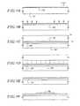
- a single crystal silicon substrate 101 as a forming material of a single crystal silicon layeris prepared.
- a P-type substrate having a main surface of a crystal face of a ⁇ 110 ⁇ planeis used, an N-type substrate may be used.
- a single crystal silicon germanium substratemay be used.
- a thermal oxidation treatmentis carried out, so that a silicon oxide film 102 is formed on the main surface (corresponding to an element forming surface).
- a film thicknessmay be suitably determined by a user, the thickness is made 10 to 500 nm (typically 20 to 50 nm).
- This silicon oxide film 102functions later as a part of a buried insulating layer of an SOI substrate ( FIG. 1A ).
- the adhesion between the single crystal silicon substrate 101 and the silicon oxide film 102becomes very high. Because, the silicon oxide film 102 is formed on the ⁇ 110 ⁇ plane in this invention, so that an interface with very high conformity can be realized. Since this interface is an interface between an active layer and an under film in a final TFT, it is very advantageous that the adhesion (conformity) is high.
- the reason why the thickness of the silicon oxide film 102 can be made as thin as 20 to 50 nmis that the crystal face of the single crystal silicon substrate 101 has the ⁇ 110 ⁇ plane, so that the silicon oxide film having high adhesion can be formed even though it is thin.
- the ⁇ 110 ⁇ planehas a problem that when an oxidation reaction proceeds, undulation (asperity) of the silicon surface gradually becomes large.
- undulationan oxidation reaction proceeds, undulation (asperity) of the silicon surface gradually becomes large.
- a problem of such undulationcan be eliminated to the utmost. This is an advantage that is common to all embodiments disclosed in the present specification.
- the single crystal silicon layer formed by using this inventionhas a very flat surface.
- a distance between the top and top of the undulationis 10 times or less (preferably 20 times or less) as long as a distance between adjacent atoms of the three atoms contained in the ⁇ 110 ⁇ plane. That is, it is about 5 nm or less (preferably 10 nm or less).
- hydrogenis added through the silicon oxide film 102 from the side of the main surface of the single crystal silicon substrate 101 .
- the hydrogen additionmay be carried out as the form of hydrogen ions using an ion implantation method.
- the addition step of hydrogenmay be carried out by other means.
- a hydrogen-containing layer 103is formed.
- a hydrogen ion with a dosage of 1 ⁇ 10 16 to 1 ⁇ 10 17 atom/cm 2is added ( FIG. 1B ).
- control of a hydrogen addition profile in the depth directionis made so that the single crystal silicon layer with a thickness of 50 nm remains between the main surface of the single crystal silicon substrate 101 and the hydrogen-containing layer 103 .
- the ⁇ 110 ⁇ planeis a plane which has the lowest atomic density, even if hydrogen ions are added, a probability of collision with silicon atoms is lowest. That is, it is possible to suppress damage at the time of ion addition to the minimum.
- the single crystal silicon substrate 101 and a supporting substrateare bonded to each other.
- a silicon substrate 104is used as the supporting substrate, and a silicon oxide film 105 for bonding is provided on its surface.
- the silicon substrate 104it is satisfactory if an inexpensive silicon substrate formed by the FZ method is prepared. Of course, it does not matter if a polycrystal silicon substrate is used. Besides, if only flatness can be assured, a highly refractory substrate such as a quartz substrate, a ceramic substrate, or a crystallized glass substrate may be used ( FIG. 1C ).
- first heat treatmentat 400 to 600° C. (typically 500° C.) is carried out.
- first heat treatmentat 400 to 600° C. (typically 500° C.) is carried out.
- the hydrogen-containing layer 103a volume change of a minute vacancy occurs, and a broken surface is produced along the hydrogen-containing layer 103 .
- the single crystal silicon substrate 101is split, so that the silicon oxide film 102 and a single crystal silicon layer 106 are made to remain on the supporting substrate ( FIG. 1D ).
- a furnace annealing stepis carried out in a temperature range of 1050 to 1150° C.
- stress relaxation of Si—O—Si bondsoccurs, so that the boned interface becomes stable. That is, this becomes a step of completely bonding the single crystal silicon layer 106 to the supporting substrate.
- this stepis carried out at 1100° C. for 2 hours.
- the bonded interfaceis stabilized in this way, so that a buried insulating layer 107 is defined.
- a dotted line in the buried insulating layer 107indicates the bonded interface, and means that adhesion of the interface has become strong.
- polishing stepcalled CMP (Chemical Mechanical Polishing) or a furnace annealing treatment at high temperature (about 900 to 1200° C.) in a reducing atmosphere may be carried out.
- CMPChemical Mechanical Polishing
- furnace annealing treatment at high temperatureabout 900 to 1200° C.
- the final thickness of the single crystal silicon layer 106may be made 10 to 200 nm (preferably 20 to 100 nm).
- the single crystal silicon layer 106is patterned to form an island-like silicon layer 108 which becomes an active layer of a TFT.
- an island-like silicon layer 108which becomes an active layer of a TFT.
- a plurality of layersare formed on the same substrate ( FIG. 1F ).
- the island-like silicon layer 108 having the main surface of the ⁇ 110 ⁇ planeis obtained.
- the present inventionis characterized in that the island-like silicon layer obtained in this way is used as an active layer of a TFT, and a plurality of TFTs are formed on the same substrate.
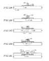
- FIGS. 2A to 2ENext, a method of forming a TFT will be described with reference to FIGS. 2A to 2E .
- steps up to the state of FIG. 1Fare completed.
- a supporting substrate 201is actually divided into the silicon substrate 104 and the buried insulating layer 107 in FIG. 1 , they are shown in an integrated state for simplicity.
- An island-like silicon layer 202 of FIG. 2Acorresponds to the island-like silicon layer 108 of FIG. 1F .
- a thermal oxidation stepis carried out so that a silicon oxide film 203 with a thickness of 10 nm is formed on the surface of the island-like silicon layer 202 .
- This silicon oxide film 203functions as a gate insulating film.
- a polysilicon film having conductivityis formed thereon, and a gate wiring line 204 is formed by patterning ( FIG. 2A ).
- the materialis not limited to this.
- a metal materialsuch as tantalum, tantalum alloy, or a laminate film of tantalum and tantalum nitride.
- itis also effective to use copper or copper alloy.
- an impurity to give N-type conductivity or P-type conductivityis added to form an impurity region 205 .
- the impurity concentration at this timedetermines the impurity concentration of an LDD region later.
- arsenic with a concentration of 1 ⁇ 10 18 atoms/cm 3is added, neither an impurity nor a concentration is not required to be limited to this embodiment.
- a thin silicon oxide film 206 with a thickness of about 5 to 10 nmis formed on the surface of the gate wiring line. This may be formed by using a thermal oxidation method or a plasma oxidation method. The formation of the silicon oxide film 206 has an object to make it function as an etching stopper in a next side wall forming step.
- a silicon nitride filmis formed and etch back is carried out, so that a side wall 207 is formed. In this way, the state of FIG. 2B is obtained.
- the silicon nitride filmis used as the side wall 207
- a polysilicon film or an amorphous silicon filmmay be used.
- the material of the gate wiring lineis changed, room for choice of a material which can be used as the side wall is widened.
- an impurity having the same conductivity as the former stepis added again.
- the concentration of the impurity added at this timeis made higher than that at the former step.
- arsenicis used as the impurity, and the concentration is made 1 ⁇ 10 21 atoms/cm 3 .
- the concentrationis made 1 ⁇ 10 21 atoms/cm 3 .
- a source region 208 , a drain region 209 , an LDD region 210 , and a channel formation region 211are defined ( FIG. 2C ).
- activation of the impurityis carried out by furnace annealing, laser annealing, lamp annealing, or the like.
- silicon oxide films formed on the surfaces of the gate wiring line 204 , the source region 208 , and the drain region 209are removed to expose their surfaces.
- a cobalt film 212 with a thickness of about 5 nmis formed and a thermal treatment step is carried out. By this heat treatment, a reaction of cobalt and silicon occurs, so that a silicide layer (cobalt silicide layer) 213 is formed ( FIG. 2D ).
- This techniqueis a well-known salicide technique. Thus, it does not matter if titanium or tungsten is used instead of cobalt, and a heat treatment condition and the like may be referred to the well-known technique.
- the heat treatment stepis carried out by using lamp annealing.
- an interlayer insulating film 214 with a thickness of 1 ⁇ mis formed.
- a silicon oxide film, a silicon nitride film, a silicon nitride oxide film, or a resin film, such as polyamide, polyimide, acryl, etc.may be used. Alternatively, these insulating films may be laminated.
- contact holesare formed in the interlayer insulating film 214 , and a source wiring line 215 and a drain wiring line 216 made of a material containing aluminum as its main ingredient are formed. Finally, the entire component is subjected to furnace annealing at 300° C. for 2 hours in a hydrogen atmosphere, and hydrogenating is completed.
- a TFT as shown in FIG. 2Eis obtained.
- the structure described in this embodimentis merely an example, and a TFT structure to which the present invention can be applied is not limited to this.
- the inventioncan be applied to a TFT of any well-known structure.
- the step condition of this embodimentis merely an example, and a user may properly determine an optimum condition other than the essential portion of the invention.
- N-channel TFTAs an example, it is also easy to fabricate a P-channel TFT. Further, it is also possible to form a CMOS circuit by forming an N-channel TFT and a P-channel TFT on the same substrate and by complementarily combining them.
- a pixel electrode(not shown) electrically connected to the drain wiring line 216 is formed by well-known means, it is also easy to form a pixel switching element of an active matrix type display device.
- the inventionis also a very effective technique as a method of fabricating an electro-optical device typified by a liquid crystal display device, an EL (electroluminescence) display device, an EC (electrochromic) display device, a photoelectric conversion device (optical sensor), and the like.
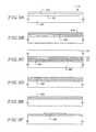
- a single crystal silicon substrate 301 having a main surface (crystal face) of a ⁇ 110 ⁇ planeis prepared.
- the main surfaceis subjected to anodization to form a porous silicon layer 302 .
- the anodization stepmay be carried out in a mixed solution of hydrofluoric acid and ethanol.
- the porous silicon layer 302is regarded as a single crystal silicon layer provided with columnar surface holes at a surface density of about 10 11 holes/cm 3 , and succeeds to the crystal state (orientation, etc.) of the single crystal silicon substrate 301 as it is. Incidentally, since the ELTRAN method itself is well known the detailed description will be omitted here.
- a heat treatment stepin a reducing atmosphere and within a temperature range of 900 to 1200° C. (preferably 1000 to 1150° C.).
- a heat treatment at 1050° C. for 2 hoursis carried out in a hydrogen atmosphere.
- the reducing atmospherealthough a hydrogen atmosphere, an ammonia atmosphere, or an inert gas atmosphere containing hydrogen or ammonia (mixed atmosphere of hydrogen and nitrogen, or hydrogen and argon, etc.) is preferable, flattening of the surface of the crystalline silicon film can be made even in an inert gas atmosphere.
- a hydrogen atmosphere, an ammonia atmosphere, or an inert gas atmosphere containing hydrogen or ammoniamixed atmosphere of hydrogen and nitrogen, or hydrogen and argon, etc.
- flattening of the surface of the crystalline silicon filmcan be made even in an inert gas atmosphere.
- a reduction of a natural oxidation filmis carried out by using a reducing action, many silicon atoms with high energy are generated and the flattening effect is resultantly increased.
- use of the reducing atmosphereis preferable.
- the concentration of oxygen or an oxygen compound (for example, OH radical) contained in the atmospheremust be 10 ppm or less (preferably 1 ppm or less). Otherwise, the reducing reaction by hydrogen comes not to occur.
- the surface holesare filled up by movement of silicon atoms, so that a very flat silicon surface can be obtained.
- a single crystal silicon layer 303is epitaxially grown on the porous silicon layer 302 .
- the epitaxially grown single crystal silicon layer 303reflects the crystal structure of the single crystal silicon substrate 301 as it is, its main surface becomes a ⁇ 110 ⁇ plane.
- the film thicknessmay be 10 to 200 nm (preferably 20 to 100 nm) ( FIG. 3A ).
- the single crystal silicon layer 303is oxidized to form a silicon oxide layer 304 .
- a forming methodit is possible to use thermal oxidation, plasma oxidation, laser oxidation, or the like.
- a single crystal silicon layer 305remains ( FIG. 3B ).
- a polycrystal silicon substrate 306 provided with a silicon oxide layer on its surfaceis prepared.
- a ceramic substrate, a quartz substrate, or a glass ceramic substrate each provided with an insulating film on its surfacemay be used.
- both of the substratesare bonded to each other in such a manner that the respective main surfaces are opposite to each other.
- the silicon oxide layer provided on each of the substratesfunctions as an adhesive ( FIG. 3C ).
- a heat treatment step at a temperature of 1050 to 1150° C.is next carried out, and the bonded interface made of both the silicon oxide layers is stabilized.
- this heat treatment stepis carried out at 1100° C. for 2 hours.
- a portion indicated by a dotted line in FIG. 3Cis the bonded interface after adhering has been completely performed.
- the silicon oxide layers provided on both the substratesare integrated by the heat treatment to become a buried insulating layer 307 .
- the single crystal silicon substrate 301is ground from the rear surface side by mechanical polishing such as CMP, and the grinding step is ended when the porous silicon layer 302 is exposed. In this way, the state shown in FIG. 3D is obtained.
- the porous silicon layer 302is subjected to wet etching and is selectively removed.
- a mixed solution of a hydrofluoric acid solution and a hydrogen peroxide solutionis preferable. It is reported that a solution of a mixture of 49% HF and 30% H 2 O 2 at a ratio of 1:5 has a selecting ratio of a hundred thousand times or more between a single crystal silicon layer and a porous silicon layer.
- the state shown in FIG. 3Eis obtained in this way.
- the buried insulating layer 307is provided on the polycrystal silicon substrate 306 , and a single crystal silicon layer 308 is formed thereon.
- the heat treatment stepis also effective in decrease of impurities.
- the obtained single crystal silicon layer 308is patterned to form an island-like silicon layer 309 .
- an island-like silicon layer 309Although only one layer is shown in the drawings, it is needless to say that a plurality of island-like silicon layers may be formed.
- a TFTcan be fabricated in accordance with the same steps as those described in embodiment 1 with reference to FIGS. 2A to 2E .
- the TFTmay be formed by other well-known means. In this embodiment, the detailed description will be omitted.
- reference numeral 401designates a single crystal silicon substrate.
- an oxygen ionis first added to the single crystal silicon substrate 401 to form an oxygen-containing layer 402 at a predetermined depth.
- the oxygen ion with a dosage of about 1 ⁇ 10 18 atoms/cm 2may be added.
- the width of the oxygen-containing layer 402 in the depth directionis determined by a distribution of the oxygen ion at the ion addition, and has a distribution with a gentle tail.
- the interface between the single crystal silicon substrate 401 and the buried insulating layer 403becomes very steep ( FIG. 4B ).
- this buried insulating layer 403is 10 to 500 nm (typically 20 to 50 nm).
- the reason why the buried insulating layer as thin as 20 to 50 nm can be realizedis that the interface between the single crystal silicon substrate 401 and the buried insulating layer 403 is stably coupled, which is the very result of the fact that the single crystal silicon substrate having the main surface of the ⁇ 110 ⁇ plane is used as the material of the single crystal silicon layer.
- a single crystal silicon layer 404remains on the buried insulating layer 403 . That is, in this embodiment, since the single crystal silicon substrate having the main surface of the ⁇ 110 ⁇ plane is used, the main surface (crystal face) of the single crystal silicon layer 404 obtained after the buried insulating layer is formed comes to have the ⁇ 110 ⁇ plane as well. Incidentally, adjustment may be made so that the thickness of the single crystal silicon layer 404 becomes 10 to 200 nm (preferably 20 to 100 nm).
- TFTsmay be completed in accordance with the steps described in embodiment 1 using FIGS. 2A to 2E .
- the TFTsmay be formed by other well-known means. In this embodiment, the detailed description will be omitted.
- FIGS. 5A to 5Can example of a reflection type liquid crystal display device as a semiconductor device of the present invention will be shown in FIGS. 5A to 5C . Since a fabricating method of a pixel TFT (pixel switching element) and a cell assembling step may be made by using well-known means, the detailed description will be omitted.
- reference numeral 11designates a substrate having an insulating surface
- 12designates a pixel matrix circuit
- 13designates a source driver circuit
- 14designates a gate driver circuit
- 15designates an opposite substrate
- 16designates an FPC (Flexible Printed Circuit)
- 17designates a signal processing circuit.
- the signal processing circuit 17a circuit performing processing for which an IC has been conventionally substituted, such as a D/A converter, a ⁇ -correction circuit, or a signal dividing circuit, can be formed.
- a D/A convertera ⁇ -correction circuit, or a signal dividing circuit
- the description in this embodimenthas been made on the liquid crystal display device as an example, it is needless to say that the present invention can be applied to an EL (electroluminescence) display device or an EC (electrochromic) display device as long as the display device is an active matrix type display device.
- an EL (electroluminescence) display device or an EC (electrochromic) display deviceas long as the display device is an active matrix type display device.
- FIG. 5Ban example of a circuit constituting the driver circuits 13 and 14 of FIG. 5A is shown in FIG. 5B . Since a TFT portion has been described in embodiment 1, only necessary portions will be described here.
- reference numerals 501 and 502designate N-channel TFTs
- 503designates a P-channel TFT
- the TFTs 501 and 503constitute a CMOS circuit.
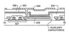
- Reference numeral 504designates an insulating layer made of a laminate film of a silicon nitride film/silicon oxide film/resin film, and a titanium wiring line 505 is provided thereon.
- the CMOS circuit and the TFT 502are electrically connected to each other.
- the titanium wiring lineis further covered with an insulating layer 506 made of a resin film.
- the two insulating films 504 and 506also have a function as a flattening film.
- FIG. 5CA part of circuits constituting the pixel matrix circuit 12 of FIG. 5A is shown in FIG. 5C .
- reference numeral 507designates a pixel TFT made of a double gate structure N-channel TFT, and a drain wiring line 508 is formed to widely extend into a pixel region.
- the insulating layer 504is provided thereon, and the titanium wiring line 505 is provided thereon. At this time, a recess portion is formed in a part of the insulating layer 504 , and only silicon nitride and silicon oxide of the lowermost layer are made to remain. By this, auxiliary capacitance is formed between the drain wiring line 508 and the titanium wiring line 505 .
- the titanium wiring line 505 provided in the pixel matrix circuithas an electric field shielding effect between the source/drain wiring line and a subsequent pixel electrode. Further, it also functions as a black mask at gaps between a plurality of pixel electrodes provided.
- the insulating layer 506is provided to cover the titanium wiring line 505 , and a pixel electrode 509 made of a reflective conductive film is formed thereon.
- a pixel electrode 509 made of a reflective conductive filmis formed thereon.
- contrivance to raise reflectivitymay be made on the surface of the pixel electrode 509 .
- the reflection type liquid crystal display device having the structure as described abovecan be fabricated by using the present invention.
- the present inventioncan be applied to all conventional IC techniques. That is, the present invention can be applied to all semiconductor circuits presently available on the market.
- the present inventionmay be applied to a microprocessor such as a RISC processor integrated on one chip or an ASIC processor, and may be applied to circuits from a signal processing circuit such as a D/A converter to a high frequency circuit for a portable equipment (portable telephone, PHS, mobile computer).
- a microprocessorsuch as a RISC processor integrated on one chip or an ASIC processor
- a signal processing circuitsuch as a D/A converter to a high frequency circuit for a portable equipment (portable telephone, PHS, mobile computer).
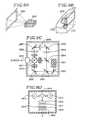
- FIG. 6shows an example of a microprocessor.
- the microprocessoris typically constituted by a CPU core 21 , a RAM 22 , a clock controller 23 , a cache memory 24 , a cache controller 25 , a serial interface 26 , an I/O port 27 , and the like.
- the microprocessor shown in FIG. 6is a simplified example, and various circuit designs are made for actual microprocessors according to their use.
- itis an IC (Integrated Circuit) 28 that functions as a central part.
- the IC 28is a functional circuit in which an integrated circuit formed on a semiconductor chip 29 is protected with ceramic or the like.
- An N-channel TFT 30 and a P-channel TFT 31 having the structure of this inventionconstitute the integrated circuit formed on the semiconductor chip 29 . Note that when a basic circuit is constituted by a CMOS circuit as a minimum unit, power consumption can be suppressed.
- the microprocessor shown in this embodimentis mounted on various electronic equipments and functions as a central circuit.
- a personal computera portable information terminal equipment, and other all household electric appliances can be enumerated.
- a computer for controlling a vehiclecan also be enumerated.
- a CMOS circuit and a pixel matrix circuit formed through carrying out the present inventionmay be applied to various electro-optical devices (active matrix type liquid crystal display devices, active matrix type EL display devices, active matrix type EC display devices). Namely, the present invention may be embodied in all the electronic equipments that incorporate those electro-optical devices as display media.
- a video camera, a digital camera, a projector (rear-type projector or front-type projector), a head mount display (goggle-type display), a navigation system for vehicles, a personal computer, and a portable information terminal (a mobile computer, a cellular phone, or an electronic book)may be enumerated. Examples of those are shown in FIGS. 7A to 8D .
- FIG. 7Ashows a personal computer comprising a main body 2001 , an image inputting unit 2002 , a display device 2003 , and a key board 2004 .
- the present inventionis applicable to the image inputting unit 2002 , the display device 2003 , and other signal control circuits.
- FIG. 7Bshows a video camera comprising a main body 2101 , a display device 2102 , a voice input unit 2103 , an operation switch 2104 , a battery 2105 , and an image receiving unit 2106 .
- the present inventionis applicable to the display device 2102 , the voice input unit 2103 , and other signal control circuits.
- FIG. 7Cshows a mobile computer comprising a main body 2201 , a camera unit 2202 , an image receiving unit 2203 , an operation switch 2204 , and a display device 2205 .
- the present inventionis applicable to the display device 2205 and other signal control circuits.
- FIG. 7Dshows a goggle-type display comprising a main body 2301 , a display device 2302 and an arm portion 2303 .
- the present inventionis applicable to the display device 2302 and other signal control circuits.
- FIG. 7Eshows a player that employs a recoding medium in which programs are recorded (hereinafter referred to as recording medium), and comprises a main body 2401 , a display device 2402 , a speaker unit 2403 , a recording medium 2404 , and an operation switch 2405 .
- this playeruses as the recoding medium a DVD (digital versatile disc), a CD and the like to serve as a tool for enjoying music or movies, for playing games and for connecting to the Internet.
- the present inventionis applicable to the display device 2402 and other signal control circuits.
- FIG. 7Fshows a digital camera comprising a main body 2501 , a display device 2502 , an eye piece section 2503 , an operation switch 2504 , and an image receiving unit (not shown).
- the present inventionis applicable to the display device 2502 and other signal control circuits.
- FIG. 8Ashows a front-type projector comprising a display device 2601 and a screen 2602 .
- the present inventionis applicable to the display device and other signal control circuits.
- FIG. 8Bshows a rear-type projector comprising a main body 2701 , a display device 2702 , a mirror 2703 , and a screen 2704 .
- the present inventionis applicable to the display device and other signal control circuits.
- FIG. 8Cis a diagram showing an example of the structure of the display devices 2601 and 2702 in FIGS. 8A and 8B .
- the display device 2601 or 2702comprises a light source optical system 2801 , mirrors 2802 and 2805 to 2807 , dichroic mirrors 2803 and 2804 , optical lenses 2808 , 2809 and 2811 , liquid crystal display devices 2810 , and a projection optical system 2812 .
- the projection optical system 2812consists of an optical system including a projection lens.
- This embodimentshows an example of “three plate type” using three liquid crystal display devices 2810 , but not particularly limited thereto. For instance, the invention may be applied also to “single plate type”.
- an optical systemsuch as an optical lens, a film having a polarization function, a film for adjusting a phase difference, an IR film may be provided on discretion of a person who carries out the invention.
- FIG. 8Dis a diagram showing an example of the structure of the light source optical system 2801 in FIG. 8C .
- the light source optical system 2801comprises light sources 2813 and 2814 , synthetic prism 2815 , collimator lenses 2816 and 2820 , lens arrays 2817 and 2818 , polarizing converter element 2819 .
- the light source optical system shown in FIG. 8Demploys two light sources, but may employ three to four of light sources, or more. Of course, it may employ one light source.
- the light source optical systemmay be provided with an optical system such as an optical lens, a film having a polarization function, a film for adjusting the phase difference, and an IR film.
- an optical systemsuch as an optical lens, a film having a polarization function, a film for adjusting the phase difference, and an IR film.
- the scope of application of the present inventionis very wide, and the invention can be applied to electronic equipments of any fields.
- the electronic equipment of this embodimentcan be realized even if any combination of embodiments 1 to 5 is used.
Landscapes
- Engineering & Computer Science (AREA)
- Microelectronics & Electronic Packaging (AREA)
- Condensed Matter Physics & Semiconductors (AREA)
- General Physics & Mathematics (AREA)
- Manufacturing & Machinery (AREA)
- Computer Hardware Design (AREA)
- Physics & Mathematics (AREA)
- Power Engineering (AREA)
- Thin Film Transistor (AREA)
- Liquid Crystal (AREA)
- Metal-Oxide And Bipolar Metal-Oxide Semiconductor Integrated Circuits (AREA)
- Element Separation (AREA)
- Recrystallisation Techniques (AREA)
Abstract
Description
This application is a continuation of U.S. application Ser. No. 11/731,415, filed on Mar. 30, 2007 now U.S. Pat No. 7,473,971 which is a continuation of U.S. application Ser. No. 10/914,357, filed on Aug. 9, 2004 now U.S. Pat. No. 7,476,576 which is a continuation of U.S. application Ser. No. 09/808,162, filed on Mar. 13, 2001 (now U.S. Pat. No. 6,803,264 issued Oct. 12, 2004) which is a divisional of U.S. application Ser. No. 09/386,782, filed on Aug. 31, 1999 (now U.S. Pat. No. 6,335,231 issued Jan. 1, 2002).
1. Field of the Invention
The present invention relates to a semiconductor device fabricated by using an SOI (Silicon on Insulator) substrate and a method of fabricating the same. Specifically, the invention relates to a semiconductor device including a thin film transistor (hereinafter referred to as TFT) formed on an SOI substrate.
Incidentally, in the present specification, the semiconductor device indicates any device capable of functioning by using semiconductor characteristics. Thus, the semiconductor device includes not only a TFT but also an electro-optical device typified by a liquid crystal display device or a photoelectric conversion device, a semiconductor circuit in which TFTs are integrated, and an electronic equipment containing such an electro-optical device or a semiconductor circuit as a part.
2. Description of the Related Art
In recent years, VLSI techniques have been remarkably developed, and attention has been paid to an SOI (Silicon on Insulator) structure for realizing low power consumption. This technique is such a technique that an active region (channel formation region) of an FET, which has been conventionally formed of bulk single crystal silicon, is made thin film single crystal silicon.
In an SOI substrate, a buried oxide film made of silicon oxide exists on single crystal silicon, and a single crystal silicon thin film is formed thereon. Various methods of fabricating such SOI substrates are known. As a typical SOI substrate, an SIMOX substrate is known. The term SIMOX is an abbreviation for Separation-by-Implanted Oxygen, and oxygen is ion implanted into a single crystal silicon substrate to form a buried oxide layer. The details of the SIMOX substrate are disclosed in [K. Izumi, M. Docken and H. Ariyoshi: “C.M.O.S. devices fabrication on buried SiO2layers formed by oxygen implantation into silicon”, Electron. Lett., 14, 593-594 (1978)].
Recently, attention has also been paid to a bonded SOI substrate. The bonded SOI substrate realizes the SO structure by bonding two silicon substrates as suggested by its name. If this technique is used, a single crystal silicon thin film can be formed also on a ceramic substrate or the like.
Among the bonded SOI substrates, in recent years, attention has been especially paid to a technique called ELTRAN (registered trademark by Canon K.K.). This technique is a method of fabricating an SO substrate using selective etching of a porous silicon layer. The particular technique of the ELTRAN method is disclosed in, K. Sakaguchi et al., “Current Progress in Epitaxial Layer Transfer (ELTRAN)”, IEICE TRANS. ELECTRON. Vol. E80 C. No. 3 pp. 378-387 March 1997, in detail.
As another SQI technique attracting attention, there is a technique called Smart-Cut (registered trademark of SOITEC Co.). The Smart-Cut method is a technique developed by SOITEC Co. in France in 1996, and is a method of fabricating a bonded SoI substrate using hydrogen embrittlement. The particular technique of the Smart-Cut method is disclosed in “Industrial Research Society (Kogyo Chosa Kai); Electronic Material, August, pp. 83-87, 1977” in detail.
When the foregoing SOI substrate is fabricated, a single crystal silicon substrate having a main surface of a crystal face of a {100} plane (crystal orientation is <100> orientation) has been used in any technique. The reason is that the {100} plane has lowest interface state density (Qss) and is suitable for a field effect transistor that is sensitive to interface characteristics.
However, with respect to the SOI substrate used for a TFT, since a single crystal silicon thin film must be formed on an insulating layer, higher priority must be given to adhesion to the insulating layer than the interface state density. That is, even if the interface state density is low, it is meaningless if the single crystal silicon thin film peels off.
The present invention has been made in view of such problems, and an object thereof is to provide a semiconductor device with high reliability by fabricating an SOI substrate suitable for a TFT and by forming TFTs on the substrate.
The structure of the present invention disclosed in the present specification is characterized by comprising the steps of:
forming a hydrogen-containing layer at a predetermined depth in a single crystal semiconductor substrate having a main surface of a {110} plane;
bonding the single crystal semiconductor substrate and a supporting substrate to each other;
splitting the single crystal semiconductor substrate by a first heat treatment along the hydrogen-containing layer;
carrying out a second heat treatment at a temperature of 900 to 1200° C.;
grinding a single crystal semiconductor layer remaining on the supporting substrate and having a main surface of a {110} plane; and
forming a plurality of TFTs each having an active layer of the single crystal semiconductor layer.
Further, another structure of the present invention is characterized by comprising the steps of:
forming a porous semiconductor layer by anodization of a single crystal semiconductor substrate having a main surface of a {110} plane;
carrying out a heat treatment to the porous semiconductor layer in a reducing atmosphere;
carrying out epitaxial growth of a single crystal semiconductor layer having a main surface of a {110} plane on the porous semiconductor layer;
bonding the single crystal semiconductor substrate and a supporting substrate to each other;
carrying out a heat treatment at a temperature of 900 to 1200° C.;
grinding the single crystal semiconductor substrate until the porous semiconductor layer is exposed;
removing the porous semiconductor layer to expose the single crystal semiconductor layer; and
forming a plurality of TFTs each having an active layer of the single crystal semiconductor layer on the supporting substrate.
Still further, another structure of the present invention is characterized by comprising the steps of:
forming an oxygen-containing layer at a predetermined depth in a single crystal semiconductor substrate having a main surface of a {110} plane;
changing the oxygen-containing layer into a buried insulating layer by a heat treatment; and
forming a plurality of TFTs each having an active layer of a single crystal semiconductor layer having a main surface of a {110} plane on the buried insulating layer.
The gist of the present invention is to use a single crystal semiconductor substrate having a main surface of a {110} plane (crystal face is a {110} plane) as a forming material of a single crystal semiconductor layer finally formed on a supporting substrate when an SOI substrate is fabricated by using an SOI technique such as SIMOX. ELTRAN, or Smart-Cut.
Incidentally, although the semiconductor mentioned here typically indicates silicon, the term also includes other semiconductors such as silicon germanium.
The reason why a single crystal semiconductor substrate having a main surface of a {110} plane is used as a forming material of a single crystal semiconductor layer will be described below. Incidentally, this description will be made using single crystal silicon as an example.
As single crystal silicon, although that formed by an FZ method and that formed by a CZ method exist, in the present invention, it is preferable to use single crystal silicon formed by the FZ method. In the CZ method which is the main stream at present, oxygen of about 2×10¹⁸atoms/cm3is contained for the purpose of relieving stress, so that there is a fear that an electron or hole mobility is lowered. Particularly, in the case where a minute TFT is formed, this comes to appear remarkably.
However, in the case where single crystal silicon is used for the SOI substrate as in the present invention, since there are many cases where the thickness of a single crystal silicon layer required for an active layer of a TFT is as very thin as 10 to 50 nm, it is not quite necessary to take stress into consideration. Thus, even if the FZ method (oxygen content is 1×10¹⁷atoms/cm3or less), which can form single crystal silicon more inexpensively than the inexpensive CZ method, is used, satisfactory effects can be obtained.
In a general SOI substrate, a single crystal silicon layer is formed on a silicon oxide film. Thus, adhesion and conformity between the silicon oxide layer and the single crystal silicon layer become important. From such a viewpoint, in the SOI substrate, when the single crystal silicon layer comes in contact with the silicon oxide layer, it is ideal that the contact of the single crystal silicon layer is realized with the most stable plane.
The plane which is in contact with the silicon oxide layer with most stably is a {110} plane. Because, in the case of the {110} plane, the plane is in contact with the silicon oxide layer through three silicon atoms. This state will be explained with reference to photographs shown inFIGS. 9A and 9B .
That is, when a single crystal silicon layer having a crystal face of the {110} plane is formed on an insulating layer, it is understood that the number of silicon atoms coming in contact with the insulating layer is three.
Like this, it is understood that three silicon atoms are contained in the {110} plane, and are adjacently arranged in a substantially triangular shape. That is, in such an arrangement state, the single crystal silicon layer is in contact with an insulating layer as an under layer, and forms stable contact which is realized through “surface”. This indicates that the single crystal silicon layer is in contact with the insulating layer as an under layer with very high adhesion.
On the other hand, in the case where the single crystal silicon comes in contact with the silicon oxide layer through another plane, for example, a {100} plane or a {111} plane, the number of silicon atoms coming in contact with the silicon oxide layer is at most two, and unstable contact is formed in which the contact is realized through “line”.
Further, as a great merit of using the single crystal silicon layer having the main surface of the {110} plane, it is possible to mention that a silicon surface is very flat. In the case where the main surface is the {110} plane, a cleavage plane appears lamellarly, and it is possible to form a surface with very few asperities.
Like this, in the present invention, first priority is given to adhesion of a single crystal silicon layer to an under layer (silicon oxide layer) in the SOI substrate, and the invention is characterized by using the single crystal silicon substrate having the crystal face of the {110} plane which has not been conventionally used. That is, the invention is characterized in that the single crystal semiconductor substrate having the main surface (crystal face) of the {110} plane is used as a material, and the SOI technique such as SIMOX, ELTRAN, or Smart-Cut is fully used, so that the SOI substrate with high reliability is formed. Incidentally, an oriental flat of the single crystal semiconductor substrate having the main surface of the {110} plane may be made a {111} plane.
Then such an SOI substrate is used, and a plurality of TFTs each having an active layer of a single crystal semiconductor thin film are formed on the same substrate, so that a semiconductor device having high reliability can be realized.
The present invention will next be described in detail with preferred embodiments described below.
[Embodiment 1]
In this embodiment, with reference toFIGS. 1A to 1F and2A to2E, a description will be made on a case where when an SOI substrate is fabricated by a Smart-Cut method, a single crystal silicon substrate having a main surface of a {110} plane is used, and a semiconductor device is fabricated by using the SOI substrate.
First, a singlecrystal silicon substrate 101 as a forming material of a single crystal silicon layer is prepared. Here, although a P-type substrate having a main surface of a crystal face of a {110} plane is used, an N-type substrate may be used. Of course, a single crystal silicon germanium substrate may be used.
Next, a thermal oxidation treatment is carried out, so that asilicon oxide film 102 is formed on the main surface (corresponding to an element forming surface). Although a film thickness may be suitably determined by a user, the thickness is made 10 to 500 nm (typically 20 to 50 nm). Thissilicon oxide film 102 functions later as a part of a buried insulating layer of an SOI substrate (FIG. 1A ).
At this time, the adhesion between the singlecrystal silicon substrate 101 and thesilicon oxide film 102 becomes very high. Because, thesilicon oxide film 102 is formed on the {110} plane in this invention, so that an interface with very high conformity can be realized. Since this interface is an interface between an active layer and an under film in a final TFT, it is very advantageous that the adhesion (conformity) is high. The reason why the thickness of thesilicon oxide film 102 can be made as thin as 20 to 50 nm is that the crystal face of the singlecrystal silicon substrate 101 has the {110} plane, so that the silicon oxide film having high adhesion can be formed even though it is thin.
Incidentally, the {110} plane has a problem that when an oxidation reaction proceeds, undulation (asperity) of the silicon surface gradually becomes large. However, in the case where a thin silicon oxide film is provided as in this embodiment, since the amount of oxidation is small, a problem of such undulation can be eliminated to the utmost. This is an advantage that is common to all embodiments disclosed in the present specification.
Thus, the single crystal silicon layer formed by using this invention has a very flat surface. For example, a distance between the top and top of the undulation is 10 times or less (preferably 20 times or less) as long as a distance between adjacent atoms of the three atoms contained in the {110} plane. That is, it is about 5 nm or less (preferably 10 nm or less).
Next, hydrogen is added through thesilicon oxide film 102 from the side of the main surface of the singlecrystal silicon substrate 101. In this case, the hydrogen addition may be carried out as the form of hydrogen ions using an ion implantation method. Of course, the addition step of hydrogen may be carried out by other means. In this way, a hydrogen-containinglayer 103 is formed. In this embodiment, a hydrogen ion with a dosage of 1×10¹⁶to 1×10¹⁷atom/cm2is added (FIG. 1B ).
Since the depth where the hydrogen-containing layer is formed determines the thickness of the single crystal silicon layer later, precise control is required. In this embodiment, control of a hydrogen addition profile in the depth direction is made so that the single crystal silicon layer with a thickness of 50 nm remains between the main surface of the singlecrystal silicon substrate 101 and the hydrogen-containinglayer 103.
Since the {110} plane is a plane which has the lowest atomic density, even if hydrogen ions are added, a probability of collision with silicon atoms is lowest. That is, it is possible to suppress damage at the time of ion addition to the minimum.
Next, the singlecrystal silicon substrate 101 and a supporting substrate are bonded to each other. In this embodiment, a silicon substrate104 is used as the supporting substrate, and asilicon oxide film 105 for bonding is provided on its surface. As the silicon substrate104, it is satisfactory if an inexpensive silicon substrate formed by the FZ method is prepared. Of course, it does not matter if a polycrystal silicon substrate is used. Besides, if only flatness can be assured, a highly refractory substrate such as a quartz substrate, a ceramic substrate, or a crystallized glass substrate may be used (FIG. 1C ).
At this time, since a bonding interface is formed of highly hydrophilic silicon oxide films, they are adhered to each other with hydrogen bonds by reaction of moisture contained in both the surfaces.
Next, a heat treatment (first heat treatment) at 400 to 600° C. (typically 500° C.) is carried out. By this heat treatment, in the hydrogen-containinglayer 103, a volume change of a minute vacancy occurs, and a broken surface is produced along the hydrogen-containinglayer 103. By this, the singlecrystal silicon substrate 101 is split, so that thesilicon oxide film 102 and a singlecrystal silicon layer 106 are made to remain on the supporting substrate (FIG. 1D ).
Next, as a second heat treatment, a furnace annealing step is carried out in a temperature range of 1050 to 1150° C. In this step, at the bonded interface, stress relaxation of Si—O—Si bonds occurs, so that the boned interface becomes stable. That is, this becomes a step of completely bonding the singlecrystal silicon layer 106 to the supporting substrate. In this embodiment, this step is carried out at 1100° C. for 2 hours.
The bonded interface is stabilized in this way, so that a buried insulatinglayer 107 is defined. InFIG. 1E , a dotted line in the buried insulatinglayer 107 indicates the bonded interface, and means that adhesion of the interface has become strong.
Next, the surface of the singlecrystal silicon layer 106 is flattened. For flattening, a polishing step called CMP (Chemical Mechanical Polishing) or a furnace annealing treatment at high temperature (about 900 to 1200° C.) in a reducing atmosphere may be carried out.
The final thickness of the singlecrystal silicon layer 106 may be made 10 to 200 nm (preferably 20 to 100 nm).
Next, the singlecrystal silicon layer 106 is patterned to form an island-like silicon layer 108 which becomes an active layer of a TFT. In this embodiment, although only one island-like silicon layer is shown, a plurality of layers are formed on the same substrate (FIG. 1F ).
In the manner as described above, the island-like silicon layer 108 having the main surface of the {110} plane is obtained. The present invention is characterized in that the island-like silicon layer obtained in this way is used as an active layer of a TFT, and a plurality of TFTs are formed on the same substrate.
Next, a method of forming a TFT will be described with reference toFIGS. 2A to 2E . First, steps up to the state ofFIG. 1F are completed. InFIG. 2A , although a supportingsubstrate 201 is actually divided into the silicon substrate104 and the buried insulatinglayer 107 inFIG. 1 , they are shown in an integrated state for simplicity. An island-like silicon layer 202 ofFIG. 2A corresponds to the island-like silicon layer 108 ofFIG. 1F .
Next, a thermal oxidation step is carried out so that asilicon oxide film 203 with a thickness of10 nm is formed on the surface of the island-like silicon layer 202. Thissilicon oxide film 203 functions as a gate insulating film. After thegate insulating film 203 is formed, a polysilicon film having conductivity is formed thereon, and agate wiring line 204 is formed by patterning (FIG. 2A ).
Incidentally, in this embodiment, although the polysilicon film having N-type conductivity is used as the gate wiring line, the material is not limited to this. Particularly, for the purpose of decreasing the resistance of the gate wiring line, it is also effective to use a metal material such as tantalum, tantalum alloy, or a laminate film of tantalum and tantalum nitride. Moreover, for the purpose of obtaining the gate wiring line with further low resistance, it is also effective to use copper or copper alloy.
After the state ofFIG. 2A is obtained, an impurity to give N-type conductivity or P-type conductivity is added to form animpurity region 205. The impurity concentration at this time determines the impurity concentration of an LDD region later. In this embodiment, although arsenic with a concentration of 1×10¹⁸atoms/cm3is added, neither an impurity nor a concentration is not required to be limited to this embodiment.
Next, a thinsilicon oxide film 206 with a thickness of about 5 to 10 nm is formed on the surface of the gate wiring line. This may be formed by using a thermal oxidation method or a plasma oxidation method. The formation of thesilicon oxide film 206 has an object to make it function as an etching stopper in a next side wall forming step.
After thesilicon oxide film 206 as an etching stopper is formed, a silicon nitride film is formed and etch back is carried out, so that aside wall 207 is formed. In this way, the state ofFIG. 2B is obtained.
In this embodiment, although the silicon nitride film is used as theside wall 207, a polysilicon film or an amorphous silicon film may be used. Of course, it is needless to say that if the material of the gate wiring line is changed, room for choice of a material which can be used as the side wall is widened.
Next, an impurity having the same conductivity as the former step is added again. The concentration of the impurity added at this time is made higher than that at the former step. In this embodiment, arsenic is used as the impurity, and the concentration is made 1×10²¹atoms/cm3. However, it is not necessary to make limitation to this. By the addition step of the impurity, asource region 208, adrain region 209, anLDD region 210, and achannel formation region 211 are defined (FIG. 2C ).
In this way, after the respective impurity regions are formed, activation of the impurity is carried out by furnace annealing, laser annealing, lamp annealing, or the like.
Next, silicon oxide films formed on the surfaces of thegate wiring line 204, thesource region 208, and thedrain region 209 are removed to expose their surfaces. Then acobalt film 212 with a thickness of about5 nm is formed and a thermal treatment step is carried out. By this heat treatment, a reaction of cobalt and silicon occurs, so that a silicide layer (cobalt silicide layer)213 is formed (FIG. 2D ).
This technique is a well-known salicide technique. Thus, it does not matter if titanium or tungsten is used instead of cobalt, and a heat treatment condition and the like may be referred to the well-known technique. In this embodiment, the heat treatment step is carried out by using lamp annealing.
After thesilicide layer 213 is formed in this way, thecobalt film 212 is removed. Thereafter, aninterlayer insulating film 214 with a thickness of 1 μm is formed. As theinterlayer insulating film 214, a silicon oxide film, a silicon nitride film, a silicon nitride oxide film, or a resin film, such as polyamide, polyimide, acryl, etc., may be used. Alternatively, these insulating films may be laminated.
Next, contact holes are formed in theinterlayer insulating film 214, and asource wiring line 215 and adrain wiring line 216 made of a material containing aluminum as its main ingredient are formed. Finally, the entire component is subjected to furnace annealing at 300° C. for 2 hours in a hydrogen atmosphere, and hydrogenating is completed.
In this way, a TFT as shown inFIG. 2E is obtained. Incidentally, the structure described in this embodiment is merely an example, and a TFT structure to which the present invention can be applied is not limited to this. Thus, the invention can be applied to a TFT of any well-known structure. Besides, the step condition of this embodiment is merely an example, and a user may properly determine an optimum condition other than the essential portion of the invention.
Besides, in this embodiment, although the description has been made with the N-channel TFT as an example, it is also easy to fabricate a P-channel TFT. Further, it is also possible to form a CMOS circuit by forming an N-channel TFT and a P-channel TFT on the same substrate and by complementarily combining them.
Further, in the structure ofFIG. 2E , if a pixel electrode (not shown) electrically connected to thedrain wiring line 216 is formed by well-known means, it is also easy to form a pixel switching element of an active matrix type display device.
That is, the invention is also a very effective technique as a method of fabricating an electro-optical device typified by a liquid crystal display device, an EL (electroluminescence) display device, an EC (electrochromic) display device, a photoelectric conversion device (optical sensor), and the like.
[Embodiment 2]
In this embodiment, a description will be made of an example in which an SOI substrate different from that ofembodiment 1 is fabricated by using a single crystal silicon substrate having a main surface of a {110} plane, and a semiconductor device is fabricated by using the SOI substrate usingFIGS. 3A to 3F . Specifically, a case where a technique called ELTRAN is used will be described.
First, a singlecrystal silicon substrate 301 having a main surface (crystal face) of a {110} plane is prepared. Next, the main surface is subjected to anodization to form aporous silicon layer 302. The anodization step may be carried out in a mixed solution of hydrofluoric acid and ethanol. Theporous silicon layer 302 is regarded as a single crystal silicon layer provided with columnar surface holes at a surface density of about 1011holes/cm3, and succeeds to the crystal state (orientation, etc.) of the singlecrystal silicon substrate 301 as it is. Incidentally, since the ELTRAN method itself is well known the detailed description will be omitted here.
After theporous silicon layer 302 is formed, it is preferable to carry out a heat treatment step in a reducing atmosphere and within a temperature range of 900 to 1200° C. (preferably 1000 to 1150° C.). In this embodiment, a heat treatment at 1050° C. for 2 hours is carried out in a hydrogen atmosphere.
As the reducing atmosphere, although a hydrogen atmosphere, an ammonia atmosphere, or an inert gas atmosphere containing hydrogen or ammonia (mixed atmosphere of hydrogen and nitrogen, or hydrogen and argon, etc.) is preferable, flattening of the surface of the crystalline silicon film can be made even in an inert gas atmosphere. However, when a reduction of a natural oxidation film is carried out by using a reducing action, many silicon atoms with high energy are generated and the flattening effect is resultantly increased. Thus, use of the reducing atmosphere is preferable.
However, attention needs to be especially paid to the point that the concentration of oxygen or an oxygen compound (for example, OH radical) contained in the atmosphere must be 10 ppm or less (preferably 1 ppm or less). Otherwise, the reducing reaction by hydrogen comes not to occur.
At this time, in the vicinity of the surface of theporous silicon layer 302, the surface holes are filled up by movement of silicon atoms, so that a very flat silicon surface can be obtained.
Next, a singlecrystal silicon layer 303 is epitaxially grown on theporous silicon layer 302. At this time, since the epitaxially grown singlecrystal silicon layer 303 reflects the crystal structure of the singlecrystal silicon substrate 301 as it is, its main surface becomes a {110} plane. The film thickness may be 10 to 200 nm (preferably 20 to 100 nm) (FIG. 3A ).
Next, the singlecrystal silicon layer 303 is oxidized to form asilicon oxide layer 304. As a forming method, it is possible to use thermal oxidation, plasma oxidation, laser oxidation, or the like. At this time, a singlecrystal silicon layer 305 remains (FIG. 3B ).
Next, as a supporting substrate, apolycrystal silicon substrate 306 provided with a silicon oxide layer on its surface is prepared. Of course, a ceramic substrate, a quartz substrate, or a glass ceramic substrate each provided with an insulating film on its surface may be used.
After the preparation of the singlecrystal silicon substrate 301 and the supporting substrate (polycrystal silicon substrate306) is completed in this way, both of the substrates are bonded to each other in such a manner that the respective main surfaces are opposite to each other. In this case, the silicon oxide layer provided on each of the substrates functions as an adhesive (FIG. 3C ).
After bonding is ended, a heat treatment step at a temperature of 1050 to 1150° C. is next carried out, and the bonded interface made of both the silicon oxide layers is stabilized. In this embodiment, this heat treatment step is carried out at 1100° C. for 2 hours. Incidentally, a portion indicated by a dotted line inFIG. 3C is the bonded interface after adhering has been completely performed. The silicon oxide layers provided on both the substrates are integrated by the heat treatment to become a buried insulatinglayer 307.
Next, the singlecrystal silicon substrate 301 is ground from the rear surface side by mechanical polishing such as CMP, and the grinding step is ended when theporous silicon layer 302 is exposed. In this way, the state shown inFIG. 3D is obtained.
Next, theporous silicon layer 302 is subjected to wet etching and is selectively removed. As an etchant to be used, a mixed solution of a hydrofluoric acid solution and a hydrogen peroxide solution is preferable. It is reported that a solution of a mixture of 49% HF and 30% H2O2at a ratio of 1:5 has a selecting ratio of a hundred thousand times or more between a single crystal silicon layer and a porous silicon layer.
The state shown inFIG. 3E is obtained in this way. In this state, the buried insulatinglayer 307 is provided on thepolycrystal silicon substrate 306, and a singlecrystal silicon layer 308 is formed thereon.
Although the SOI substrate is completed at this time, since minute asperities exist on the surface of the singlecrystal silicon layer 308, it is desirable to carry out a heat treatment step in a hydrogen atmosphere to perform flattening. This flattening phenomenon occurs due to speed-increasing surface diffusion of silicon atoms by reduction of a natural oxidation film.
At this time, since there is also an effect that boron contained in the single crystal silicon layer308 (that contained in a P-type silicon substrate) is released into a vapor phase by hydrogen atoms, the heat treatment step is also effective in decrease of impurities.
Next, the obtained singlecrystal silicon layer 308 is patterned to form an island-like silicon layer 309. Although only one layer is shown in the drawings, it is needless to say that a plurality of island-like silicon layers may be formed.
Thereafter, a TFT can be fabricated in accordance with the same steps as those described inembodiment 1 with reference toFIGS. 2A to 2E . The TFT may be formed by other well-known means. In this embodiment, the detailed description will be omitted.
[Embodiment 3]
In this embodiment, a description will be made on an example in which a single crystal silicon substrate having a main surface of a {110} plane is used to fabricate an SOI substrate different from that ofembodiment 1 or embodiment 2, and a semiconductor device is fabricated by using the substrate usingFIGS. 4A to 4C . Specifically, a case in which an SOI substrate called SIMOX is fabricated will be described.
InFIG. 4A , reference numeral401 designates a single crystal silicon substrate. In this embodiment, an oxygen ion is first added to the single crystal silicon substrate401 to form an oxygen-containinglayer 402 at a predetermined depth. The oxygen ion with a dosage of about 1×10¹⁸atoms/cm2may be added.
At this time, since the {110} plane has small atomic density, a probability of collision of the oxygen ion and silicon atom becomes lower. That is, it is possible to suppress damage of the silicon surface due to the addition of oxygen to the minimum. Of course, if the substrate temperature is raised at 400 to 600° C. during the ion addition, the damage can be further decreased.
Next, a heat treatment at a temperature of 800 to 1200° C. is carried out, so that the oxygen-containinglayer 402 is changed into a buried insulatinglayer 403. The width of the oxygen-containinglayer 402 in the depth direction is determined by a distribution of the oxygen ion at the ion addition, and has a distribution with a gentle tail. However, by this heat treatment, the interface between the single crystal silicon substrate401 and the buried insulatinglayer 403 becomes very steep (FIG. 4B ).
The thickness of this buried insulatinglayer 403 is 10 to 500 nm (typically 20 to 50 nm). The reason why the buried insulating layer as thin as 20 to 50 nm can be realized is that the interface between the single crystal silicon substrate401 and the buried insulatinglayer 403 is stably coupled, which is the very result of the fact that the single crystal silicon substrate having the main surface of the {110} plane is used as the material of the single crystal silicon layer.
When the buried insulatinglayer 403 is formed in this way, a singlecrystal silicon layer 404 remains on the buried insulatinglayer 403. That is, in this embodiment, since the single crystal silicon substrate having the main surface of the {110} plane is used, the main surface (crystal face) of the singlecrystal silicon layer 404 obtained after the buried insulating layer is formed comes to have the {110} plane as well. Incidentally, adjustment may be made so that the thickness of the singlecrystal silicon layer 404 becomes 10 to 200 nm (preferably 20 to 100 nm).
After the singlecrystal silicon layer 404 is obtained in this way, patterning is carried out to obtain an island-like silicon layer 405. A plurality of island-like silicon layers may be formed.
Thereafter, a plurality of TFTs may be completed in accordance with the steps described inembodiment 1 usingFIGS. 2A to 2E . The TFTs may be formed by other well-known means. In this embodiment, the detailed description will be omitted.
[Embodiment 4]
In this embodiment, an example of a reflection type liquid crystal display device as a semiconductor device of the present invention will be shown inFIGS. 5A to 5C . Since a fabricating method of a pixel TFT (pixel switching element) and a cell assembling step may be made by using well-known means, the detailed description will be omitted.
InFIG. 5A ,reference numeral 11 designates a substrate having an insulating surface,12 designates a pixel matrix circuit,13 designates a source driver circuit,14 designates a gate driver circuit,15 designates an opposite substrate,16 designates an FPC (Flexible Printed Circuit), and17 designates a signal processing circuit. As thesignal processing circuit 17, a circuit performing processing for which an IC has been conventionally substituted, such as a D/A converter, a γ-correction circuit, or a signal dividing circuit, can be formed. Of course, it is also possible to provide an IC chip on a glass substrate and to perform signal processing on the IC chip.
Further, although the description in this embodiment has been made on the liquid crystal display device as an example, it is needless to say that the present invention can be applied to an EL (electroluminescence) display device or an EC (electrochromic) display device as long as the display device is an active matrix type display device. Here, an example of a circuit constituting thedriver circuits FIG. 5A is shown inFIG. 5B . Since a TFT portion has been described inembodiment 1, only necessary portions will be described here.
InFIG. 5B ,reference numerals TFTs Reference numeral 504 designates an insulating layer made of a laminate film of a silicon nitride film/silicon oxide film/resin film, and atitanium wiring line 505 is provided thereon. The CMOS circuit and theTFT 502 are electrically connected to each other. The titanium wiring line is further covered with an insulatinglayer 506 made of a resin film. The two insulatingfilms
A part of circuits constituting thepixel matrix circuit 12 ofFIG. 5A is shown inFIG. 5C . InFIG. 5C ,reference numeral 507 designates a pixel TFT made of a double gate structure N-channel TFT, and adrain wiring line 508 is formed to widely extend into a pixel region.
The insulatinglayer 504 is provided thereon, and thetitanium wiring line 505 is provided thereon. At this time, a recess portion is formed in a part of the insulatinglayer 504, and only silicon nitride and silicon oxide of the lowermost layer are made to remain. By this, auxiliary capacitance is formed between thedrain wiring line 508 and thetitanium wiring line 505.
Besides, thetitanium wiring line 505 provided in the pixel matrix circuit has an electric field shielding effect between the source/drain wiring line and a subsequent pixel electrode. Further, it also functions as a black mask at gaps between a plurality of pixel electrodes provided.
Then, the insulatinglayer 506 is provided to cover thetitanium wiring line 505, and apixel electrode 509 made of a reflective conductive film is formed thereon. Of course, it does not matter if contrivance to raise reflectivity may be made on the surface of thepixel electrode 509.
Actually, although an orientation film or a liquid crystal layer is provided on thepixel electrode 509, the description will be omitted here.
The reflection type liquid crystal display device having the structure as described above can be fabricated by using the present invention. Of course, when combined with a well-known technique, it is also possible to easily fabricate a transmission type liquid crystal display device. Further, when combined with a well-known technique, it is also possible to easily fabricate an active matrix type EL display device.
[Embodiment 5]
The present invention can be applied to all conventional IC techniques. That is, the present invention can be applied to all semiconductor circuits presently available on the market. For example, the present invention may be applied to a microprocessor such as a RISC processor integrated on one chip or an ASIC processor, and may be applied to circuits from a signal processing circuit such as a D/A converter to a high frequency circuit for a portable equipment (portable telephone, PHS, mobile computer).
An N-channel TFT 30 and a P-channel TFT 31 having the structure of this invention constitute the integrated circuit formed on thesemiconductor chip 29. Note that when a basic circuit is constituted by a CMOS circuit as a minimum unit, power consumption can be suppressed.
Besides, the microprocessor shown in this embodiment is mounted on various electronic equipments and functions as a central circuit. As typical electronic equipments, a personal computer, a portable information terminal equipment, and other all household electric appliances can be enumerated. Besides, a computer for controlling a vehicle (automobile, electric train, etc.) can also be enumerated.
[Embodiment 6]
A CMOS circuit and a pixel matrix circuit formed through carrying out the present invention may be applied to various electro-optical devices (active matrix type liquid crystal display devices, active matrix type EL display devices, active matrix type EC display devices). Namely, the present invention may be embodied in all the electronic equipments that incorporate those electro-optical devices as display media.
As such an electronic equipment, a video camera, a digital camera, a projector (rear-type projector or front-type projector), a head mount display (goggle-type display), a navigation system for vehicles, a personal computer, and a portable information terminal (a mobile computer, a cellular phone, or an electronic book) may be enumerated. Examples of those are shown inFIGS. 7A to 8D .
The light source optical system shown inFIG. 8D employs two light sources, but may employ three to four of light sources, or more. Of course, it may employ one light source.
Further, on discretion of a person who carries out the invention, the light source optical system may be provided with an optical system such as an optical lens, a film having a polarization function, a film for adjusting the phase difference, and an IR film.
As described above, the scope of application of the present invention is very wide, and the invention can be applied to electronic equipments of any fields. The electronic equipment of this embodiment can be realized even if any combination ofembodiments 1 to 5 is used.
Claims (24)
1. An electronic equipment comprising:
a transistor including:
an island-like single crystalline semiconductor layer comprising silicon disposed over a silicon substrate with at least a first silicon oxide layer and a second silicon oxide layer interposed therebetween, wherein the island-like single crystalline semiconductor layer is in contact with the first silicon oxide layer and has at least a channel formation region, a source region and a drain region;
a gate insulating film formed on the island-like single crystalline semiconductor layer; and
a gate wiring line formed over the channel formation region with the gate insulating film interposed therebetween; and
an interlayer insulating film formed over the transistor,
wherein the first and second silicon oxide layers are bonded to each other with a bonded interface therebetween,
wherein the island-like single crystalline semiconductor layer is 20 to 100 nm thick,
wherein the island-like single crystalline semiconductor layer is formed from a part of another single crystal silicon substrate,
wherein the interlayer insulating film comprises silicon nitride and is in direct contact with at least an upper surface of the gate wiring line,
wherein the interlayer insulating film is in direct contact with at least a portion of the source region and the drain region, and
wherein the first silicon oxide layer is an oxide layer which is formed by thermally oxidizing silicon.
2. The electronic equipment according toclaim 1 wherein the island-like single crystalline semiconductor layer has a main surface of a {110} plane.
3. The electronic equipment according toclaim 1 wherein the first silicon oxide layer is in direct contact with the island-like single crystalline semiconductor layer and is 10 to 500 nm thick.
4. The electronic equipment according toclaim 1 wherein the island-like single crystalline semiconductor layer is hydrogenated.
5. The electronic equipment according toclaim 1 wherein the source region and the drain region are in contact with the first silicon oxide layer.
6. The electronic equipment according toclaim 1 wherein the island-like single crystalline semiconductor layer contains oxygen and a concentration of the oxygen is 1×10¹⁷atoms/cm3or less.
7. The electronic equipment according toclaim 1 wherein an upper surface of the gate wiring line and at least a part of the source region and the drain region comprise a metal silicide.
8. The electronic equipment according toclaim 1 , wherein the island-like single crystalline semiconductor layer contains oxygen and a concentration of the oxygen is less than 2×10¹⁸atoms/cm3.
9. An electronic equipment comprising:
an N-channel transistor including:
an island-like single crystalline semiconductor layer comprising silicon disposed over a silicon substrate with at least a first silicon oxide layer and a second silicon oxide layer interposed therebetween, wherein the island-like single crystalline semiconductor layer is in contact with the first silicon oxide layer and has at least two channel formation regions, a source region and a drain region;
a gate insulating film formed on the island-like single crystalline semiconductor layer; and
at least two gate wiring lines formed over the two channel formation regions with the gate insulating film interposed therebetween; and
an interlayer insulating film formed over the N-channel transistor,
wherein the interlayer insulating film comprises silicon nitride and is in direct contact with at least an upper surface of the two gate wiring lines,
wherein the first and second silicon oxide layers are bonded to each other with a bonded interface therebetween,
wherein the island-like single crystalline semiconductor layer is 20 to 100 nm thick,
wherein the island-like single crystalline semiconductor layer is formed from a part of another single crystal silicon substrate,
wherein the island-like single crystalline semiconductor layer contains oxygen and a concentration of the oxygen is less than 2×10¹⁸atoms/cm3,
wherein the interlayer insulating film is in direct contact with at least a portion of the source region and the drain region, and
wherein the first silicon oxide layer is an oxide layer which is formed by thermally oxidizing silicon.
10. The electronic equipment according toclaim 9 wherein the concentration of the oxygen is 1×10¹⁷atoms/cm3or less.
11. The electronic equipment according toclaim 9 wherein the island-like single crystalline semiconductor layer has a main surface of a {110} plane.
12. An electronic equipment comprising:
an N-channel transistor including:
an island-like single crystalline semiconductor layer comprising silicon disposed over a silicon substrate with at least a first silicon oxide layer and a second silicon oxide layer interposed therebetween, wherein the island-like single crystalline semiconductor layer is in contact with the first silicon oxide layer and has at least two channel formation regions, a source region and a drain region;
a gate insulating film formed on the island-like single crystalline semiconductor layer;
at least two gate wiring lines formed over the two channel formation regions with the gate insulating film interposed therebetween;
silicon oxide films formed on side surfaces of the two gate wiring lines; and
side walls formed adjacent to the side surfaces of the two gate wiring lines with the silicon oxide films therebetween;
a first interlayer insulating film comprising silicon nitride formed over the N-channel transistor; and
a second interlayer insulating film comprising silicon nitride formed over the first interlayer insulating film,
wherein the first and second silicon oxide layers are bonded to each other with a bonded interface therebetween,
wherein the island-like single crystalline semiconductor layer is 20 to 100 nm thick,
wherein upper portions of the source region and the drain region of the N-channel transistor comprise a metal silicide,
wherein the island-like single crystalline semiconductor layer is formed from a part of another single crystal silicon substrate,
wherein the first interlayer insulating film comprises silicon nitride and is in direct contact with the side walls,
wherein the island-like single crystalline semiconductor layer contains oxygen and a concentration of the oxygen is less than 2×10¹⁸atoms/cm3,
wherein the first interlayer insulating film is in direct contact with at least a portion of the source region and the drain region, and
wherein the first silicon oxide layer is an oxide layer which is formed by thermally oxidizing silicon.
13. The electronic equipment according toclaim 12 wherein the island-like single crystalline semiconductor layer has a main surface of a {110} plane.
14. The electronic equipment according toclaim 12 wherein the first silicon oxide layer is in direct contact with the island-like single crystalline semiconductor layer and is 10 to 500 nm thick.
15. The electronic equipment according toclaim 12 wherein the metal silicide is a cobalt silicide.
16. The electronic equipment according toclaim 12 wherein the island-like single crystalline semiconductor layer is hydrogenated.
17. The electronic equipment according toclaim 12 wherein the source region and the drain region are in contact with the first silicon oxide layer.
18. The electronic equipment according toclaim 12 wherein the concentration of the oxygen is 1 ×10¹⁷atoms/cm3or less.
19. A semiconductor device comprising:
a transistor including:
an island-like single crystalline semiconductor layer comprising silicon disposed over a silicon substrate with at least a first silicon oxide layer and a second silicon oxide layer interposed therebetween, wherein the island-like single crystalline semiconductor layer is in contact with the first silicon oxide layer and has at least a channel formation region, a source region and a drain region;
a gate insulating film formed on the island-like single crystalline semiconductor layer;
a gate wiring line formed over the channel formation region with the gate insulating film interposed therebetween;
silicon oxide films formed on side surfaces of the gate wiring line; and
side walls comprising silicon nitride formed adjacent to the side surfaces of the gate wiring line with the silicon oxide films interposed therebetween, and
an interlayer insulating film comprising silicon nitride formed over the transistor, the interlayer insulating film being in contact with at least an upper surface of the gate wiring line,
wherein the first and second silicon oxide layers are bonded to each other with a bonded interface therebetween,
wherein the island-like single crystalline semiconductor layer is 20 to 100 nm thick,
wherein the interlayer insulating film is in direct contact with at least a portion of the source region and the drain region, and
wherein the first silicon oxide layer is an oxide layer which is formed by thermally oxidizing silicon.
20. The semiconductor device according toclaim 19 wherein the island-like single crystalline semiconductor layer has a main surface of a {110} plane.
21. The semiconductor device according toclaim 19 wherein the source region and the drain region are in contact with the first silicon oxide layer.
22. The semiconductor device according toclaim 19 wherein an upper surface of the gate wiring line and at least a part of the source region and the drain region comprise a metal silicide.
23. The semiconductor device according toclaim 19 wherein the island-like single crystalline semiconductor layer is hydrogenated.
24. The semiconductor device according toclaim 19 , wherein the island-like single crystalline semiconductor layer contains oxygen and a concentration of the oxygen is less than 2×10¹⁸atoms/cm3.
Priority Applications (1)
| Application Number | Priority Date | Filing Date | Title |
|---|---|---|---|
| US11/926,623US9070604B2 (en) | 1998-09-04 | 2007-10-29 | Method of fabricating a semiconductor device |
Applications Claiming Priority (7)
| Application Number | Priority Date | Filing Date | Title |
|---|---|---|---|
| JP10-251635 | 1998-09-04 | ||
| JP25163598 | 1998-09-04 | ||
| US09/386,782US6335231B1 (en) | 1998-09-04 | 1999-08-31 | Method of fabricating a high reliable SOI substrate |
| US09/808,162US6803264B2 (en) | 1998-09-04 | 2001-03-13 | Method of fabricating a semiconductor device |
| US10/914,357US7476576B2 (en) | 1998-09-04 | 2004-08-09 | Method of fabricating a semiconductor device |
| US11/731,415US7473971B2 (en) | 1998-09-04 | 2007-03-30 | Method of fabricating a semiconductor device |
| US11/926,623US9070604B2 (en) | 1998-09-04 | 2007-10-29 | Method of fabricating a semiconductor device |
Related Parent Applications (1)
| Application Number | Title | Priority Date | Filing Date |
|---|---|---|---|
| US11/731,415ContinuationUS7473971B2 (en) | 1998-09-04 | 2007-03-30 | Method of fabricating a semiconductor device |
Publications (2)
| Publication Number | Publication Date |
|---|---|
| US20080070335A1 US20080070335A1 (en) | 2008-03-20 |
| US9070604B2true US9070604B2 (en) | 2015-06-30 |
Family
ID=17225761
Family Applications (13)
| Application Number | Title | Priority Date | Filing Date |
|---|---|---|---|
| US09/386,782Expired - LifetimeUS6335231B1 (en) | 1998-09-04 | 1999-08-31 | Method of fabricating a high reliable SOI substrate |
| US09/808,162Expired - Fee RelatedUS6803264B2 (en) | 1998-09-04 | 2001-03-13 | Method of fabricating a semiconductor device |
| US10/914,357CeasedUS7476576B2 (en) | 1998-09-04 | 2004-08-09 | Method of fabricating a semiconductor device |
| US11/731,415CeasedUS7473971B2 (en) | 1998-09-04 | 2007-03-30 | Method of fabricating a semiconductor device |
| US11/926,598Expired - Fee RelatedUS8405090B2 (en) | 1998-09-04 | 2007-10-29 | Method of fabricating a semiconductor device |
| US11/926,552Expired - Fee RelatedUS7642598B2 (en) | 1998-09-04 | 2007-10-29 | Method of fabricating a semiconductor device |
| US11/926,573CeasedUS7473592B2 (en) | 1998-09-04 | 2007-10-29 | Method of fabricating a semiconductor device |
| US11/926,623Expired - Fee RelatedUS9070604B2 (en) | 1998-09-04 | 2007-10-29 | Method of fabricating a semiconductor device |
| US11/926,520Expired - Fee RelatedUS7638805B2 (en) | 1998-09-04 | 2007-10-29 | Method of fabricating a semiconductor device |
| US12/418,334Expired - Fee RelatedUSRE42097E1 (en) | 1998-09-04 | 2009-04-03 | Method of fabricating a semiconductor device |
| US12/418,280Expired - Fee RelatedUSRE42139E1 (en) | 1998-09-04 | 2009-04-03 | Method of fabricating a semiconductor device |
| US12/418,245Expired - Fee RelatedUSRE42241E1 (en) | 1998-09-04 | 2009-04-03 | Method of fabricating a semiconductor device |
| US12/428,497AbandonedUS20090236698A1 (en) | 1998-09-04 | 2009-04-23 | Method of fabricating a semiconductor device |
Family Applications Before (7)
| Application Number | Title | Priority Date | Filing Date |
|---|---|---|---|
| US09/386,782Expired - LifetimeUS6335231B1 (en) | 1998-09-04 | 1999-08-31 | Method of fabricating a high reliable SOI substrate |
| US09/808,162Expired - Fee RelatedUS6803264B2 (en) | 1998-09-04 | 2001-03-13 | Method of fabricating a semiconductor device |
| US10/914,357CeasedUS7476576B2 (en) | 1998-09-04 | 2004-08-09 | Method of fabricating a semiconductor device |
| US11/731,415CeasedUS7473971B2 (en) | 1998-09-04 | 2007-03-30 | Method of fabricating a semiconductor device |
| US11/926,598Expired - Fee RelatedUS8405090B2 (en) | 1998-09-04 | 2007-10-29 | Method of fabricating a semiconductor device |
| US11/926,552Expired - Fee RelatedUS7642598B2 (en) | 1998-09-04 | 2007-10-29 | Method of fabricating a semiconductor device |
| US11/926,573CeasedUS7473592B2 (en) | 1998-09-04 | 2007-10-29 | Method of fabricating a semiconductor device |
Family Applications After (5)
| Application Number | Title | Priority Date | Filing Date |
|---|---|---|---|
| US11/926,520Expired - Fee RelatedUS7638805B2 (en) | 1998-09-04 | 2007-10-29 | Method of fabricating a semiconductor device |
| US12/418,334Expired - Fee RelatedUSRE42097E1 (en) | 1998-09-04 | 2009-04-03 | Method of fabricating a semiconductor device |
| US12/418,280Expired - Fee RelatedUSRE42139E1 (en) | 1998-09-04 | 2009-04-03 | Method of fabricating a semiconductor device |
| US12/418,245Expired - Fee RelatedUSRE42241E1 (en) | 1998-09-04 | 2009-04-03 | Method of fabricating a semiconductor device |
| US12/428,497AbandonedUS20090236698A1 (en) | 1998-09-04 | 2009-04-23 | Method of fabricating a semiconductor device |
Country Status (2)
| Country | Link |
|---|---|
| US (13) | US6335231B1 (en) |
| JP (7) | JP4476390B2 (en) |
Cited By (1)
| Publication number | Priority date | Publication date | Assignee | Title |
|---|---|---|---|---|
| US9922866B2 (en) | 2015-07-31 | 2018-03-20 | International Business Machines Corporation | Enhancing robustness of SOI substrate containing a buried N+ silicon layer for CMOS processing |
Families Citing this family (196)
| Publication number | Priority date | Publication date | Assignee | Title |
|---|---|---|---|---|
| TW408351B (en)* | 1997-10-17 | 2000-10-11 | Semiconductor Energy Lab | Semiconductor device and method of manufacturing the same |
| US6686623B2 (en) | 1997-11-18 | 2004-02-03 | Semiconductor Energy Laboratory Co., Ltd. | Nonvolatile memory and electronic apparatus |
| JP2000012864A (en)* | 1998-06-22 | 2000-01-14 | Semiconductor Energy Lab Co Ltd | Method for manufacturing semiconductor device |
| US6271101B1 (en)* | 1998-07-29 | 2001-08-07 | Semiconductor Energy Laboratory Co., Ltd. | Process for production of SOI substrate and process for production of semiconductor device |
| US6559036B1 (en)* | 1998-08-07 | 2003-05-06 | Semiconductor Energy Laboratory Co., Ltd. | Semiconductor device and method of manufacturing the same |
| JP4476390B2 (en) | 1998-09-04 | 2010-06-09 | 株式会社半導体エネルギー研究所 | Method for manufacturing semiconductor device |
| TW518650B (en)* | 1999-04-15 | 2003-01-21 | Semiconductor Energy Lab | Electro-optical device and electronic equipment |
| US6777274B2 (en)* | 2000-01-25 | 2004-08-17 | Samsung Electronics Co., Ltd. | Low temperature polycrystalline silicon type thin film transistor and a method of the thin film transistor fabrication |
| FR2816445B1 (en)* | 2000-11-06 | 2003-07-25 | Commissariat Energie Atomique | METHOD FOR MANUFACTURING A STACKED STRUCTURE COMPRISING A THIN LAYER ADHERING TO A TARGET SUBSTRATE |
| JP3716755B2 (en)* | 2001-04-05 | 2005-11-16 | 株式会社日立製作所 | Active matrix display device |
| TW487958B (en)* | 2001-06-07 | 2002-05-21 | Ind Tech Res Inst | Manufacturing method of thin film transistor panel |
| US8195187B2 (en)* | 2001-06-25 | 2012-06-05 | Airvana Network Solutions, Inc. | Radio network control |
| US7501303B2 (en)* | 2001-11-05 | 2009-03-10 | The Trustees Of Boston University | Reflective layer buried in silicon and method of fabrication |
| US20050140283A1 (en)* | 2002-02-13 | 2005-06-30 | Lau Silvanus S. | Multilayer structure to form an active matrix display having single crystalline drivers over a transmissive substrate |
| FR2874455B1 (en)* | 2004-08-19 | 2008-02-08 | Soitec Silicon On Insulator | HEAT TREATMENT BEFORE BONDING TWO PLATES |
| US6953736B2 (en)* | 2002-07-09 | 2005-10-11 | S.O.I.Tec Silicon On Insulator Technologies S.A. | Process for transferring a layer of strained semiconductor material |
| FR2842350B1 (en)* | 2002-07-09 | 2005-05-13 | METHOD FOR TRANSFERRING A LAYER OF CONCEALED SEMICONDUCTOR MATERIAL | |
| JP4454921B2 (en)* | 2002-09-27 | 2010-04-21 | 株式会社半導体エネルギー研究所 | Method for manufacturing semiconductor device |
| JP4683817B2 (en)* | 2002-09-27 | 2011-05-18 | 株式会社半導体エネルギー研究所 | Method for manufacturing semiconductor device |
| US6707106B1 (en) | 2002-10-18 | 2004-03-16 | Advanced Micro Devices, Inc. | Semiconductor device with tensile strain silicon introduced by compressive material in a buried oxide layer |
| JP2004172406A (en)* | 2002-11-20 | 2004-06-17 | Kobe Steel Ltd | Semiconductor substrate with ceramics, semiconductor wafer with ceramics, and its manufacturing method |
| US7176528B2 (en)* | 2003-02-18 | 2007-02-13 | Corning Incorporated | Glass-based SOI structures |
| US7399681B2 (en)* | 2003-02-18 | 2008-07-15 | Corning Incorporated | Glass-based SOI structures |
| EP1596437A4 (en)* | 2003-02-19 | 2009-12-02 | Shinetsu Handotai Kk | Method for manufacturing soi wafer and soi wafer |
| US6911379B2 (en)* | 2003-03-05 | 2005-06-28 | Taiwan Semiconductor Manufacturing Company, Ltd. | Method of forming strained silicon on insulator substrate |
| US6949451B2 (en)* | 2003-03-10 | 2005-09-27 | Taiwan Semiconductor Manufacturing Company, Ltd. | SOI chip with recess-resistant buried insulator and method of manufacturing the same |
| US6902962B2 (en)* | 2003-04-04 | 2005-06-07 | Taiwan Semiconductor Manufacturing Company, Ltd. | Silicon-on-insulator chip with multiple crystal orientations |
| JP4342826B2 (en) | 2003-04-23 | 2009-10-14 | 株式会社半導体エネルギー研究所 | Manufacturing method of semiconductor element |
| US6864149B2 (en)* | 2003-05-09 | 2005-03-08 | Taiwan Semiconductor Manufacturing Company | SOI chip with mesa isolation and recess resistant regions |
| JP4239676B2 (en)* | 2003-05-15 | 2009-03-18 | 信越半導体株式会社 | SOI wafer and manufacturing method thereof |
| US7538010B2 (en) | 2003-07-24 | 2009-05-26 | S.O.I.Tec Silicon On Insulator Technologies | Method of fabricating an epitaxially grown layer |
| FR2857983B1 (en)* | 2003-07-24 | 2005-09-02 | Soitec Silicon On Insulator | PROCESS FOR PRODUCING AN EPITAXIC LAYER |
| JP2005070120A (en)* | 2003-08-27 | 2005-03-17 | Shin Etsu Chem Co Ltd | Pellicle for lithography |
| US7625808B2 (en)* | 2003-09-01 | 2009-12-01 | Sumco Corporation | Method for manufacturing bonded wafer |
| JP4554180B2 (en)* | 2003-09-17 | 2010-09-29 | ソニー株式会社 | Method for manufacturing thin film semiconductor device |
| WO2005041292A1 (en)* | 2003-10-24 | 2005-05-06 | Sony Corporation | Method for manufacturing semiconductor substrate and semiconductor substrate |
| US6902965B2 (en)* | 2003-10-31 | 2005-06-07 | Taiwan Semiconductor Manufacturing Company, Ltd. | Strained silicon structure |
| US7161169B2 (en)* | 2004-01-07 | 2007-01-09 | International Business Machines Corporation | Enhancement of electron and hole mobilities in <110> Si under biaxial compressive strain |
| FR2864970B1 (en)* | 2004-01-09 | 2006-03-03 | Soitec Silicon On Insulator | SUPPORT SUBSTRATE WITH THERMAL EXPANSION COEFFICIENT DETERMINED |
| US7205210B2 (en)* | 2004-02-17 | 2007-04-17 | Freescale Semiconductor, Inc. | Semiconductor structure having strained semiconductor and method therefor |
| JP2005311295A (en)* | 2004-03-26 | 2005-11-04 | Semiconductor Energy Lab Co Ltd | Semiconductor device |
| US7279751B2 (en)* | 2004-06-21 | 2007-10-09 | Matsushita Electric Industrial Co., Ltd. | Semiconductor laser device and manufacturing method thereof |
| DE102004032917B4 (en)* | 2004-07-07 | 2010-01-28 | Qimonda Ag | Method for producing a double-gate transistor |
| US7560361B2 (en)* | 2004-08-12 | 2009-07-14 | International Business Machines Corporation | Method of forming gate stack for semiconductor electronic device |
| KR101140450B1 (en)* | 2004-08-18 | 2012-04-30 | 코닝 인코포레이티드 | Strained semiconductor-on-insulator structure and methods for making strained semiconductor-on-insulator structures |
| KR101121798B1 (en)* | 2004-08-18 | 2012-03-20 | 코닝 인코포레이티드 | High strain glass/glass-ceramic containing semiconductor-on-insulator structures |
| JP4816856B2 (en)* | 2004-09-15 | 2011-11-16 | 信越半導体株式会社 | Manufacturing method of SOI wafer |
| US7422956B2 (en)* | 2004-12-08 | 2008-09-09 | Advanced Micro Devices, Inc. | Semiconductor device and method of making semiconductor device comprising multiple stacked hybrid orientation layers |
| US7348610B2 (en)* | 2005-02-24 | 2008-03-25 | International Business Machines Corporation | Multiple layer and crystal plane orientation semiconductor substrate |
| US20060205129A1 (en)* | 2005-02-25 | 2006-09-14 | Semiconductor Energy Laboratory Co., Ltd. | Method for manufacturing semiconductor device |
| WO2006093817A2 (en)* | 2005-02-28 | 2006-09-08 | Silicon Genesis Corporation | Substrate stiffness method and resulting devices |
| US7659892B2 (en)* | 2005-03-17 | 2010-02-09 | Semiconductor Energy Laboratory Co., Ltd. | Display device and portable terminal |
| US7687372B2 (en)* | 2005-04-08 | 2010-03-30 | Versatilis Llc | System and method for manufacturing thick and thin film devices using a donee layer cleaved from a crystalline donor |
| WO2006117900A1 (en)* | 2005-04-26 | 2006-11-09 | Sharp Kabushiki Kaisha | Process for producing semiconductor device and semiconductor device |
| JP2007019191A (en)* | 2005-07-06 | 2007-01-25 | Fujitsu Ltd | Semiconductor device and manufacturing method thereof |
| US7268051B2 (en)* | 2005-08-26 | 2007-09-11 | Corning Incorporated | Semiconductor on glass insulator with deposited barrier layer |
| US7691730B2 (en)* | 2005-11-22 | 2010-04-06 | Corning Incorporated | Large area semiconductor on glass insulator |
| FR2896619B1 (en)* | 2006-01-23 | 2008-05-23 | Soitec Silicon On Insulator | PROCESS FOR MANUFACTURING A COMPOSITE SUBSTRATE WITH IMPROVED ELECTRIC PROPERTIES |
| FR2896618B1 (en)* | 2006-01-23 | 2008-05-23 | Soitec Silicon On Insulator | PROCESS FOR PRODUCING A COMPOSITE SUBSTRATE |
| JP5168788B2 (en)* | 2006-01-23 | 2013-03-27 | 信越半導体株式会社 | Manufacturing method of SOI wafer |
| JP4467628B2 (en)* | 2006-03-08 | 2010-05-26 | シャープ株式会社 | Manufacturing method of semiconductor device |
| US7696024B2 (en)* | 2006-03-31 | 2010-04-13 | Semiconductor Energy Laboratory Co., Ltd. | Semiconductor device and manufacturing method thereof |
| US20070264796A1 (en)* | 2006-05-12 | 2007-11-15 | Stocker Mark A | Method for forming a semiconductor on insulator structure |
| ATE518241T1 (en)* | 2007-01-24 | 2011-08-15 | Soitec Silicon On Insulator | PRODUCTION PROCESS FOR SILICON WAFER ON INSULATOR AND CORRESPONDING WAFER |
| US7755113B2 (en)* | 2007-03-16 | 2010-07-13 | Semiconductor Energy Laboratory Co., Ltd. | Semiconductor device, semiconductor display device, and manufacturing method of semiconductor device |
| WO2008123117A1 (en)* | 2007-03-26 | 2008-10-16 | Semiconductor Energy Laboratory Co., Ltd. | Soi substrate and method for manufacturing soi substrate |
| WO2008123116A1 (en) | 2007-03-26 | 2008-10-16 | Semiconductor Energy Laboratory Co., Ltd. | Soi substrate and method for manufacturing soi substrate |
| WO2008121262A2 (en)* | 2007-03-30 | 2008-10-09 | Corning Incorporated | Glass-ceramic-based semiconductor-on-insulator structures and method for making the same |
| CN101281912B (en) | 2007-04-03 | 2013-01-23 | 株式会社半导体能源研究所 | Soi substrate and manufacturing method thereof, and semiconductor device |
| US7875881B2 (en)* | 2007-04-03 | 2011-01-25 | Semiconductor Energy Laboratory Co., Ltd. | Memory device and semiconductor device |
| US20080248629A1 (en)* | 2007-04-06 | 2008-10-09 | Semiconductor Energy Laboratory Co., Ltd. | Method for manufacturing semiconductor substrate |
| KR101362688B1 (en)* | 2007-04-13 | 2014-02-17 | 가부시키가이샤 한도오따이 에네루기 켄큐쇼 | Photovoltaic device and method for manufacturing the same |
| WO2008132894A1 (en)* | 2007-04-13 | 2008-11-06 | Semiconductor Energy Laboratory Co., Ltd. | Display device, method for manufacturing display device, and soi substrate |
| KR101440930B1 (en)* | 2007-04-20 | 2014-09-15 | 가부시키가이샤 한도오따이 에네루기 켄큐쇼 | Manufacturing method of SOI substrate |
| EP1986230A2 (en)* | 2007-04-25 | 2008-10-29 | Semiconductor Energy Laboratory Co., Ltd. | Method of manufacturing SOI substrate and method of manufacturing semiconductor device |
| EP1986229A1 (en)* | 2007-04-27 | 2008-10-29 | S.O.I.T.E.C. Silicon on Insulator Technologies | Method for manufacturing compound material wafer and corresponding compound material wafer |
| KR101436115B1 (en)* | 2007-04-27 | 2014-09-01 | 가부시키가이샤 한도오따이 에네루기 켄큐쇼 | Method of manufacturing semiconductor substrate and method of manufacturing semiconductor device |
| JP5289805B2 (en)* | 2007-05-10 | 2013-09-11 | 株式会社半導体エネルギー研究所 | Method for manufacturing substrate for manufacturing semiconductor device |
| KR101443580B1 (en)* | 2007-05-11 | 2014-10-30 | 가부시키가이샤 한도오따이 에네루기 켄큐쇼 | Method for manufacturing semiconductor device |
| JP5137461B2 (en)* | 2007-05-15 | 2013-02-06 | 株式会社半導体エネルギー研究所 | Semiconductor device |
| KR101457656B1 (en)* | 2007-05-17 | 2014-11-04 | 가부시키가이샤 한도오따이 에네루기 켄큐쇼 | Method of manufacturing semiconductor device, method of manufacturing display device, semiconductor device, display device and electronic device |
| EP1993128A3 (en)* | 2007-05-17 | 2010-03-24 | Semiconductor Energy Laboratory Co., Ltd. | Method for manufacturing soi substrate |
| US8513678B2 (en)* | 2007-05-18 | 2013-08-20 | Semiconductor Energy Laboratory Co., Ltd. | Light-emitting device |
| EP1993126B1 (en)* | 2007-05-18 | 2011-09-21 | Semiconductor Energy Laboratory Co., Ltd. | Manufacturing methods of semiconductor substrate |
| US7960262B2 (en)* | 2007-05-18 | 2011-06-14 | Semiconductor Energy Laboratory Co., Ltd. | Method for manufacturing semiconductor device by applying laser beam to single-crystal semiconductor layer and non-single-crystal semiconductor layer through cap film |
| EP1993127B1 (en)* | 2007-05-18 | 2013-04-24 | Semiconductor Energy Laboratory Co., Ltd. | Manufacturing method of SOI substrate |
| WO2008142911A1 (en)* | 2007-05-18 | 2008-11-27 | Semiconductor Energy Laboratory Co., Ltd. | Semiconductor device and method for manufacturing the same |
| US9059247B2 (en)* | 2007-05-18 | 2015-06-16 | Semiconductor Energy Laboratory Co., Ltd. | Method for manufacturing SOI substrate and method for manufacturing semiconductor device |
| US8803781B2 (en)* | 2007-05-18 | 2014-08-12 | Semiconductor Energy Laboratory Co., Ltd. | Semiconductor device and display device |
| KR101400699B1 (en)* | 2007-05-18 | 2014-05-29 | 가부시키가이샤 한도오따이 에네루기 켄큐쇼 | Semiconductor substrate, semiconductor device and manufacturing method thereof |
| JP2008300709A (en)* | 2007-06-01 | 2008-12-11 | Semiconductor Energy Lab Co Ltd | Semiconductor device, and manufacturing method thereof |
| JP5142831B2 (en)* | 2007-06-14 | 2013-02-13 | 株式会社半導体エネルギー研究所 | Semiconductor device and manufacturing method thereof |
| US7772054B2 (en) | 2007-06-15 | 2010-08-10 | Semiconductor Energy Laboratory Co., Ltd. | Method for manufacturing semiconductor device |
| US7875532B2 (en)* | 2007-06-15 | 2011-01-25 | Semiconductor Energy Laboratory Co., Ltd. | Substrate for manufacturing semiconductor device and manufacturing method thereof |
| US7781306B2 (en)* | 2007-06-20 | 2010-08-24 | Semiconductor Energy Laboratory Co., Ltd. | Semiconductor substrate and method for manufacturing the same |
| US7763502B2 (en) | 2007-06-22 | 2010-07-27 | Semiconductor Energy Laboratory Co., Ltd | Semiconductor substrate, method for manufacturing semiconductor substrate, semiconductor device, and electronic device |
| KR101484296B1 (en) | 2007-06-26 | 2015-01-19 | 가부시키가이샤 한도오따이 에네루기 켄큐쇼 | Semiconductor substrate, manufacturing method of the semiconductor substrate, and semiconductor device and electronic device using the same |
| US7795111B2 (en)* | 2007-06-27 | 2010-09-14 | Semiconductor Energy Laboratory Co., Ltd. | Manufacturing method of SOI substrate and manufacturing method of semiconductor device |
| US8354674B2 (en)* | 2007-06-29 | 2013-01-15 | Semiconductor Energy Laboratory Co., Ltd. | Semiconductor device wherein a property of a first semiconductor layer is different from a property of a second semiconductor layer |
| EP2009687B1 (en)* | 2007-06-29 | 2016-08-17 | Semiconductor Energy Laboratory Co., Ltd. | Method of manufacturing an SOI substrate and method of manufacturing a semiconductor device |
| EP2009694A3 (en)* | 2007-06-29 | 2017-06-21 | Semiconductor Energy Laboratory Co, Ltd. | Semiconductor device and manufacturing method thereof |
| US20090004764A1 (en)* | 2007-06-29 | 2009-01-01 | Semiconductor Energy Laboratory Co., Ltd. | Method for manufacturing SOI substrate and method for manufacturing semiconductor device |
| US7678668B2 (en)* | 2007-07-04 | 2010-03-16 | Semiconductor Energy Laboratory Co., Ltd. | Manufacturing method of SOI substrate and manufacturing method of semiconductor device |
| US8049253B2 (en) | 2007-07-11 | 2011-11-01 | Semiconductor Energy Laboratory Co., Ltd. | Semiconductor device and method for manufacturing the same |
| US7790563B2 (en)* | 2007-07-13 | 2010-09-07 | Semiconductor Energy Laboratory Co., Ltd. | Semiconductor device, electronic device and method for manufacturing semiconductor device |
| JP5486781B2 (en)* | 2007-07-19 | 2014-05-07 | 株式会社半導体エネルギー研究所 | Method for manufacturing semiconductor device |
| JP5442224B2 (en)* | 2007-07-23 | 2014-03-12 | 株式会社半導体エネルギー研究所 | Manufacturing method of SOI substrate |
| JP5135935B2 (en) | 2007-07-27 | 2013-02-06 | 信越半導体株式会社 | Manufacturing method of bonded wafer |
| US20090032873A1 (en)* | 2007-07-30 | 2009-02-05 | Jeffrey Scott Cites | Ultra thin single crystalline semiconductor TFT and process for making same |
| US8114722B2 (en)* | 2007-08-24 | 2012-02-14 | Semiconductor Energy Laboratory Co., Ltd. | Manufacturing method of semiconductor device |
| JP5205012B2 (en) | 2007-08-29 | 2013-06-05 | 株式会社半導体エネルギー研究所 | Display device and electronic apparatus including the display device |
| JP2009076890A (en)* | 2007-08-31 | 2009-04-09 | Semiconductor Energy Lab Co Ltd | Manufacturing method of semiconductor device, semiconductor device, and electronic device |
| US8314009B2 (en)* | 2007-09-14 | 2012-11-20 | Semiconductor Energy Laboratory Co., Ltd. | Method for manufacturing SOI substrate and method for manufacturing semiconductor device |
| CN101796613B (en)* | 2007-09-14 | 2012-06-27 | 株式会社半导体能源研究所 | Semiconductor devices and electronic equipment |
| US8232598B2 (en)* | 2007-09-20 | 2012-07-31 | Semiconductor Energy Laboratory Co., Ltd. | Display device and method for manufacturing the same |
| JP5463017B2 (en)* | 2007-09-21 | 2014-04-09 | 株式会社半導体エネルギー研究所 | Substrate manufacturing method |
| JP5325404B2 (en)* | 2007-09-21 | 2013-10-23 | 株式会社半導体エネルギー研究所 | Method for manufacturing SOI substrate |
| KR101499175B1 (en)* | 2007-10-04 | 2015-03-05 | 가부시키가이샤 한도오따이 에네루기 켄큐쇼 | Method for manufacturing semiconductor substrate |
| JP5490393B2 (en)* | 2007-10-10 | 2014-05-14 | 株式会社半導体エネルギー研究所 | Manufacturing method of semiconductor substrate |
| US8236668B2 (en)* | 2007-10-10 | 2012-08-07 | Semiconductor Energy Laboratory Co., Ltd. | Method for manufacturing SOI substrate |
| US8455331B2 (en)* | 2007-10-10 | 2013-06-04 | Semiconductor Energy Laboratory Co., Ltd. | Manufacturing method of semiconductor device |
| US7799658B2 (en) | 2007-10-10 | 2010-09-21 | Semiconductor Energy Laboratory Co., Ltd. | Method for manufacturing semiconductor substrate and method for manufacturing semiconductor device |
| JP5506172B2 (en) | 2007-10-10 | 2014-05-28 | 株式会社半導体エネルギー研究所 | Method for manufacturing semiconductor substrate |
| US7989305B2 (en)* | 2007-10-10 | 2011-08-02 | Semiconductor Energy Laboratory Co., Ltd. | Method for manufacturing SOI substrate using cluster ion |
| JP5511173B2 (en)* | 2007-10-10 | 2014-06-04 | 株式会社半導体エネルギー研究所 | Method for manufacturing semiconductor device |
| JP2009135430A (en) | 2007-10-10 | 2009-06-18 | Semiconductor Energy Lab Co Ltd | Method for manufacturing semiconductor device |
| US8101501B2 (en)* | 2007-10-10 | 2012-01-24 | Semiconductor Energy Laboratory Co., Ltd. | Method of manufacturing semiconductor device |
| JP5527956B2 (en)* | 2007-10-10 | 2014-06-25 | 株式会社半導体エネルギー研究所 | Manufacturing method of semiconductor substrate |
| TWI493609B (en) | 2007-10-23 | 2015-07-21 | Semiconductor Energy Lab | Semiconductor substrate, display panel, and method of manufacturing display device |
| SG170089A1 (en)* | 2007-10-29 | 2011-04-29 | Semiconductor Energy Lab | Formation method of single crystal semiconductor layer, formation method of crystalline semiconductor layer, formation method of polycrystalline layer, and method for manufacturing semiconductor device |
| WO2009057669A1 (en)* | 2007-11-01 | 2009-05-07 | Semiconductor Energy Laboratory Co., Ltd. | Method for manufacturing photoelectric conversion device |
| US8163628B2 (en)* | 2007-11-01 | 2012-04-24 | Semiconductor Energy Laboratory Co., Ltd. | Method for manufacturing semiconductor substrate |
| US7851318B2 (en) | 2007-11-01 | 2010-12-14 | Semiconductor Energy Laboratory Co., Ltd. | Semiconductor substrate and method for manufacturing the same, and method for manufacturing semiconductor device |
| JP5548351B2 (en)* | 2007-11-01 | 2014-07-16 | 株式会社半導体エネルギー研究所 | Method for manufacturing semiconductor device |
| US7816234B2 (en) | 2007-11-05 | 2010-10-19 | Semiconductor Energy Laboratory Co., Ltd. | Method for manufacturing semiconductor device |
| US20090124038A1 (en)* | 2007-11-14 | 2009-05-14 | Mark Ewing Tuttle | Imager device, camera, and method of manufacturing a back side illuminated imager |
| JP2009151293A (en)* | 2007-11-30 | 2009-07-09 | Semiconductor Energy Lab Co Ltd | Display device, method for manufacturing display device, and electronic apparatus |
| JP5464843B2 (en)* | 2007-12-03 | 2014-04-09 | 株式会社半導体エネルギー研究所 | Method for manufacturing SOI substrate |
| US20090141004A1 (en)* | 2007-12-03 | 2009-06-04 | Semiconductor Energy Laboratory Co., Ltd. | Display device and method for manufacturing the same |
| JP5459900B2 (en)* | 2007-12-25 | 2014-04-02 | 株式会社半導体エネルギー研究所 | Method for manufacturing semiconductor device |
| US7842583B2 (en) | 2007-12-27 | 2010-11-30 | Semiconductor Energy Laboratory Co., Ltd. | Method for manufacturing semiconductor substrate and method for manufacturing semiconductor device |
| US20090179160A1 (en)* | 2008-01-16 | 2009-07-16 | Semiconductor Energy Laboratory Co., Ltd. | Semiconductor substrate manufacturing apparatus |
| JP5404064B2 (en) | 2008-01-16 | 2014-01-29 | 株式会社半導体エネルギー研究所 | Laser processing apparatus and semiconductor substrate manufacturing method |
| JP5503876B2 (en)* | 2008-01-24 | 2014-05-28 | 株式会社半導体エネルギー研究所 | Manufacturing method of semiconductor substrate |
| US20090212397A1 (en)* | 2008-02-22 | 2009-08-27 | Mark Ewing Tuttle | Ultrathin integrated circuit and method of manufacturing an ultrathin integrated circuit |
| US8003483B2 (en) | 2008-03-18 | 2011-08-23 | Semiconductor Energy Laboratory Co., Ltd. | Method for manufacturing SOI substrate |
| JP2009231376A (en)* | 2008-03-19 | 2009-10-08 | Shin Etsu Handotai Co Ltd | Soi wafer and semiconductor device, and method of manufacturing the soi wafer |
| JP2009260313A (en)* | 2008-03-26 | 2009-11-05 | Semiconductor Energy Lab Co Ltd | Method for manufacturing soi substrate, and method for manufacturing semiconductor device |
| EP2105957A3 (en)* | 2008-03-26 | 2011-01-19 | Semiconductor Energy Laboratory Co., Ltd. | Method for manufacturing soi substrate and method for manufacturing semiconductor device |
| JP2009260315A (en)* | 2008-03-26 | 2009-11-05 | Semiconductor Energy Lab Co Ltd | Method for manufacturing soi substrate, and method for manufacturing semiconductor device |
| JP5654206B2 (en)* | 2008-03-26 | 2015-01-14 | 株式会社半導体エネルギー研究所 | Method for manufacturing SOI substrate and semiconductor device using the SOI substrate |
| US7939389B2 (en) | 2008-04-18 | 2011-05-10 | Semiconductor Energy Laboratory Co., Ltd. | Semiconductor device and method for manufacturing the same |
| JP5503895B2 (en)* | 2008-04-25 | 2014-05-28 | 株式会社半導体エネルギー研究所 | Semiconductor device |
| JP5700617B2 (en) | 2008-07-08 | 2015-04-15 | 株式会社半導体エネルギー研究所 | Method for manufacturing SOI substrate |
| JP5552276B2 (en)* | 2008-08-01 | 2014-07-16 | 株式会社半導体エネルギー研究所 | Method for manufacturing SOI substrate |
| JP5580010B2 (en)* | 2008-09-05 | 2014-08-27 | 株式会社半導体エネルギー研究所 | Method for manufacturing semiconductor device |
| JP5478166B2 (en)* | 2008-09-11 | 2014-04-23 | 株式会社半導体エネルギー研究所 | Method for manufacturing semiconductor device |
| TWI514595B (en) | 2008-09-24 | 2015-12-21 | Semiconductor Energy Lab | Photoelectric conversion device and method of manufacturing same |
| SG160302A1 (en)* | 2008-09-29 | 2010-04-29 | Semiconductor Energy Lab | Method for manufacturing semiconductor substrate |
| US8048754B2 (en)* | 2008-09-29 | 2011-11-01 | Semiconductor Energy Laboratory Co., Ltd. | Method for manufacturing SOI substrate and method for manufacturing single crystal semiconductor layer |
| US20100081251A1 (en)* | 2008-09-29 | 2010-04-01 | Semiconductor Energy Laboratory Co., Ltd. | Method for manufacturing soi substrate |
| US8741740B2 (en)* | 2008-10-02 | 2014-06-03 | Semiconductor Energy Laboratory Co., Ltd. | Method for manufacturing SOI substrate |
| JP2010114431A (en) | 2008-10-10 | 2010-05-20 | Semiconductor Energy Lab Co Ltd | Method of manufacturing soi substrate |
| SG161151A1 (en) | 2008-10-22 | 2010-05-27 | Semiconductor Energy Lab | Soi substrate and method for manufacturing the same |
| JP5611571B2 (en)* | 2008-11-27 | 2014-10-22 | 株式会社半導体エネルギー研究所 | Method for manufacturing semiconductor substrate and method for manufacturing semiconductor device |
| SG182208A1 (en)* | 2008-12-15 | 2012-07-30 | Semiconductor Energy Lab | Manufacturing method of soi substrate and manufacturing method of semiconductor device |
| JP5503995B2 (en)* | 2009-02-13 | 2014-05-28 | 株式会社半導体エネルギー研究所 | Method for manufacturing semiconductor device |
| SG183670A1 (en)* | 2009-04-22 | 2012-09-27 | Semiconductor Energy Lab | Method of manufacturing soi substrate |
| US8278187B2 (en)* | 2009-06-24 | 2012-10-02 | Semiconductor Energy Laboratory Co., Ltd. | Method for reprocessing semiconductor substrate by stepwise etching with at least two etching treatments |
| KR20120032487A (en)* | 2009-06-24 | 2012-04-05 | 가부시키가이샤 한도오따이 에네루기 켄큐쇼 | Method reprocessing semiconductor substrate and method for manufacturing soi substrate |
| SG178061A1 (en)* | 2009-08-25 | 2012-03-29 | Semiconductor Energy Lab | Method for reprocessing semiconductor substrate, method for manufacturing reprocessed semiconductor substrate, and method for manufacturing soi substrate |
| US8318588B2 (en)* | 2009-08-25 | 2012-11-27 | Semiconductor Energy Laboratory Co., Ltd. | Method for reprocessing semiconductor substrate, method for manufacturing reprocessed semiconductor substrate, and method for manufacturing SOI substrate |
| KR101731809B1 (en)* | 2009-10-09 | 2017-05-02 | 가부시키가이샤 한도오따이 에네루기 켄큐쇼 | Reprocessing method of semiconductor substrate, manufacturing method of reprocessed semiconductor substrate, and manufacturing method of soi substrate |
| JP5926887B2 (en)* | 2010-02-03 | 2016-05-25 | 株式会社半導体エネルギー研究所 | Method for manufacturing SOI substrate |
| US9608119B2 (en) | 2010-03-02 | 2017-03-28 | Micron Technology, Inc. | Semiconductor-metal-on-insulator structures, methods of forming such structures, and semiconductor devices including such structures |
| US8513722B2 (en) | 2010-03-02 | 2013-08-20 | Micron Technology, Inc. | Floating body cell structures, devices including same, and methods for forming same |
| US8507966B2 (en) | 2010-03-02 | 2013-08-13 | Micron Technology, Inc. | Semiconductor cells, arrays, devices and systems having a buried conductive line and methods for forming the same |
| US8288795B2 (en) | 2010-03-02 | 2012-10-16 | Micron Technology, Inc. | Thyristor based memory cells, devices and systems including the same and methods for forming the same |
| US9646869B2 (en) | 2010-03-02 | 2017-05-09 | Micron Technology, Inc. | Semiconductor devices including a diode structure over a conductive strap and methods of forming such semiconductor devices |
| JP5755931B2 (en) | 2010-04-28 | 2015-07-29 | 株式会社半導体エネルギー研究所 | Method for producing semiconductor film, method for producing electrode, method for producing secondary battery, and method for producing solar cell |
| US8519387B2 (en)* | 2010-07-26 | 2013-08-27 | Semiconductor Energy Laboratory Co., Ltd. | Semiconductor device and method for manufacturing |
| TWI500118B (en) | 2010-11-12 | 2015-09-11 | Semiconductor Energy Lab | Semiconductor substrate manufacturing method |
| JP2012156495A (en) | 2011-01-07 | 2012-08-16 | Semiconductor Energy Lab Co Ltd | Manufacturing method of soi substrate |
| US8598621B2 (en) | 2011-02-11 | 2013-12-03 | Micron Technology, Inc. | Memory cells, memory arrays, methods of forming memory cells, and methods of forming a shared doped semiconductor region of a vertically oriented thyristor and a vertically oriented access transistor |
| US8952418B2 (en) | 2011-03-01 | 2015-02-10 | Micron Technology, Inc. | Gated bipolar junction transistors |
| US8519431B2 (en) | 2011-03-08 | 2013-08-27 | Micron Technology, Inc. | Thyristors |
| US8802534B2 (en) | 2011-06-14 | 2014-08-12 | Semiconductor Energy Laboratory Co., Ltd. | Method for forming SOI substrate and apparatus for forming the same |
| US9123529B2 (en) | 2011-06-21 | 2015-09-01 | Semiconductor Energy Laboratory Co., Ltd. | Method for reprocessing semiconductor substrate, method for manufacturing reprocessed semiconductor substrate, and method for manufacturing SOI substrate |
| US8772848B2 (en) | 2011-07-26 | 2014-07-08 | Micron Technology, Inc. | Circuit structures, memory circuitry, and methods |
| CN103890908B (en)* | 2011-10-18 | 2016-08-24 | 富士电机株式会社 | The stripping means of the supporting substrates of solid phase bound wafer and the manufacture method of semiconductor device |
| JP5831165B2 (en)* | 2011-11-21 | 2015-12-09 | 富士通株式会社 | Semiconductor optical device |
| US10002968B2 (en) | 2011-12-14 | 2018-06-19 | Semiconductor Energy Laboratory Co., Ltd. | Semiconductor device and display device including the same |
| US20150050816A1 (en)* | 2013-08-19 | 2015-02-19 | Korea Atomic Energy Research Institute | Method of electrochemically preparing silicon film |
| US9087689B1 (en) | 2014-07-11 | 2015-07-21 | Inoso, Llc | Method of forming a stacked low temperature transistor and related devices |
| FI128442B (en)* | 2017-06-21 | 2020-05-15 | Turun Yliopisto | Silicon-on-insulator with crystalline silicon oxide |
| KR20220045831A (en) | 2020-10-06 | 2022-04-13 | 삼성전자주식회사 | image sensor |
Citations (192)
| Publication number | Priority date | Publication date | Assignee | Title |
|---|---|---|---|---|
| US3964941A (en) | 1971-06-21 | 1976-06-22 | Motorola, Inc. | Method of making isolated complementary monolithic insulated gate field effect transistors |
| US4217153A (en) | 1977-04-04 | 1980-08-12 | Mitsubishi Denki Kabushiki Kaisha | Method of manufacturing semiconductor device |
| JPS55130897A (en)* | 1979-03-30 | 1980-10-11 | Chiyou Lsi Gijutsu Kenkyu Kumiai | Silicon single crystal |
| US4583122A (en) | 1982-06-02 | 1986-04-15 | Hitachi, Ltd. | Imaging display device |
| JPS6249629A (en)* | 1986-03-24 | 1987-03-04 | Sony Corp | Semiconductor device |
| JPS6292361A (en)* | 1985-10-17 | 1987-04-27 | Toshiba Corp | Complementary semiconductor device |
| US4665419A (en) | 1982-03-26 | 1987-05-12 | Fujitsu Limited | Semiconductor device |
| US4733947A (en)* | 1984-10-26 | 1988-03-29 | Ngk Insulators, Ltd. | Multicolor liquid crystal display panel |
| US4753896A (en) | 1986-11-21 | 1988-06-28 | Texas Instruments Incorporated | Sidewall channel stop process |
| US4768076A (en) | 1984-09-14 | 1988-08-30 | Hitachi, Ltd. | Recrystallized CMOS with different crystal planes |
| US4786955A (en) | 1987-02-24 | 1988-11-22 | General Electric Company | Semiconductor device with source and drain depth extenders and a method of making the same |
| JPS63318779A (en) | 1987-06-22 | 1988-12-27 | Sanyo Electric Co Ltd | Manufacture of semiconductor device |
| US4822752A (en)* | 1986-03-07 | 1989-04-18 | Agency Of Industrial Science And Technology | Process for producing single crystal semiconductor layer and semiconductor device produced by said process |
| JPH01264254A (en) | 1988-04-15 | 1989-10-20 | Agency Of Ind Science & Technol | Manufacture of laminate type semiconductor device |
| US4878957A (en) | 1988-03-31 | 1989-11-07 | Kabushiki Kaisha Toshiba | Dielectrically isolated semiconductor substrate |
| US4899202A (en) | 1988-07-08 | 1990-02-06 | Texas Instruments Incorporated | High performance silicon-on-insulator transistor with body node to source node connection |
| US4933298A (en) | 1987-12-18 | 1990-06-12 | Fujitsu Limited | Method of making high speed semiconductor device having a silicon-on-insulator structure |
| US4943837A (en) | 1987-03-11 | 1990-07-24 | Hitachi, Ltd. | Thin film semiconductor device and method of fabricating the same |
| JPH02260442A (en) | 1989-03-30 | 1990-10-23 | Toshiba Corp | Dielectric isolation type semiconductor substrate |
| JPH0242725Y2 (en) | 1984-12-27 | 1990-11-14 | ||
| US5002630A (en) | 1989-06-06 | 1991-03-26 | Rapro Technology | Method for high temperature thermal processing with reduced convective heat loss |
| US5015598A (en)* | 1989-11-03 | 1991-05-14 | U.S. Philips Corporation | Method of manufacturing a device comprising MIS transistors having a gate electrode in the form of an inverted "T" |
| US5060035A (en) | 1989-07-13 | 1991-10-22 | Mitsubishi Denki Kabushiki Kaisha | Silicon-on-insulator metal oxide semiconductor device having conductive sidewall structure |
| US5059304A (en) | 1988-02-12 | 1991-10-22 | Chevron Research Company | Process for removing sulfur from a hydrocarbon feedstream using a sulfur sorbent with alkali metal components or alkaline earth metal components |
| JPH0379035B2 (en) | 1984-05-28 | 1991-12-17 | Taito Kk | |
| EP0485233A2 (en) | 1990-11-09 | 1992-05-13 | Sel Semiconductor Energy Laboratory Co., Ltd. | A method of manufacturing insulated-gate field effect transistors |
| US5130770A (en) | 1990-06-19 | 1992-07-14 | Brevatome | Integrated circuit in silicon on insulator technology comprising a field effect transistor |
| JPH04206766A (en) | 1990-11-30 | 1992-07-28 | Hitachi Ltd | Manufacturing method of semiconductor device |
| JPH04242958A (en) | 1990-12-26 | 1992-08-31 | Fujitsu Ltd | Manufacturing method of semiconductor substrate |
| JPH04348532A (en) | 1991-05-27 | 1992-12-03 | Hitachi Ltd | Semiconductor device and its manufacturing method |
| US5215931A (en) | 1989-06-13 | 1993-06-01 | Texas Instruments Incorporated | Method of making extended body contact for semiconductor over insulator transistor |
| JPH05166689A (en) | 1991-11-19 | 1993-07-02 | Sumitomo Metal Mining Co Ltd | Method for joining semiconductor substrates |
| JPH05211128A (en) | 1991-09-18 | 1993-08-20 | Commiss Energ Atom | Method for manufacturing thin semiconductor material film |
| JPH05218410A (en) | 1992-01-31 | 1993-08-27 | Toshiba Corp | Semiconductor device and manufacture thereof |
| JPH05217994A (en) | 1992-01-31 | 1993-08-27 | Canon Inc | Manufacture of semiconductor substrate |
| JPH05226620A (en) | 1992-02-18 | 1993-09-03 | Fujitsu Ltd | Semiconductor substrate and manufacturing method thereof |
| US5243213A (en) | 1990-07-09 | 1993-09-07 | Sony Corporation | Mis semiconductor device formed by utilizing soi substrate having a semiconductor thin film formed on a substrate through an insulating layer |
| US5258323A (en) | 1992-12-29 | 1993-11-02 | Honeywell Inc. | Single crystal silicon on quartz |
| US5261999A (en) | 1991-05-08 | 1993-11-16 | North American Philips Corporation | Process for making strain-compensated bonded silicon-on-insulator material free of dislocations |
| JPH05315355A (en) | 1992-05-12 | 1993-11-26 | Oki Electric Ind Co Ltd | Mosfet of soi structure and manufacture thereof |
| JPH05323362A (en) | 1991-12-19 | 1993-12-07 | Seiko Instr Inc | Semiconductor device and its production |
| US5289030A (en)* | 1991-03-06 | 1994-02-22 | Semiconductor Energy Laboratory Co., Ltd. | Semiconductor device with oxide layer |
| US5317236A (en) | 1990-12-31 | 1994-05-31 | Kopin Corporation | Single crystal silicon arrayed devices for display panels |
| US5317433A (en) | 1991-12-02 | 1994-05-31 | Canon Kabushiki Kaisha | Image display device with a transistor on one side of insulating layer and liquid crystal on the other side |
| US5341028A (en)* | 1990-10-09 | 1994-08-23 | Mitsubishi Denki Kabushiki Kaisha | Semiconductor device and a method of manufacturing thereof |
| US5371037A (en) | 1990-08-03 | 1994-12-06 | Canon Kabushiki Kaisha | Semiconductor member and process for preparing semiconductor member |
| US5387555A (en) | 1992-09-03 | 1995-02-07 | Harris Corporation | Bonded wafer processing with metal silicidation |
| US5403759A (en) | 1992-10-02 | 1995-04-04 | Texas Instruments Incorporated | Method of making thin film transistor and a silicide local interconnect |
| US5424230A (en)* | 1992-02-19 | 1995-06-13 | Casio Computer Co., Ltd. | Method of manufacturing a polysilicon thin film transistor |
| US5426062A (en) | 1992-12-04 | 1995-06-20 | Texas Instruments Incorporated | Method for forming a silicon on insulator device |
| JPH07169974A (en) | 1993-09-20 | 1995-07-04 | Semiconductor Energy Lab Co Ltd | Semiconductor device and manufacturing method thereof |
| US5453394A (en) | 1992-01-31 | 1995-09-26 | Canon Kabushiki Kaisha | Process for preparing semiconductor substrate by bringing first and second substrates in contact |
| JPH07249749A (en) | 1994-03-11 | 1995-09-26 | Canon Inc | Method for manufacturing SOI substrate |
| JPH07335903A (en) | 1994-06-13 | 1995-12-22 | Semiconductor Energy Lab Co Ltd | Active matrix circuit |
| US5508209A (en) | 1993-10-01 | 1996-04-16 | Semiconductor Energy Laboratory Co., Ltd. | Method for fabricating thin film transistor using anodic oxidation |
| US5529937A (en) | 1993-07-27 | 1996-06-25 | Semiconductor Energy Laboratory Co., Ltd. | Process for fabricating thin film transistor |
| EP0723286A2 (en) | 1995-01-18 | 1996-07-24 | Canon Kabushiki Kaisha | Field-effect transistor and manufacture method thereof |
| US5550070A (en) | 1993-12-27 | 1996-08-27 | Sharp Kabushiki Kaisha | Method for producing crystalline semiconductor film having reduced concentration of catalyst elements for crystallization and semiconductor device having the same |
| US5573961A (en) | 1995-11-09 | 1996-11-12 | Taiwan Semiconductor Manufacturing Company Ltd. | Method of making a body contact for a MOSFET device fabricated in an SOI layer |
| US5574292A (en) | 1992-05-13 | 1996-11-12 | Seiko Instruments Inc. | Semiconductor device with monosilicon layer |
| US5576556A (en)* | 1993-08-20 | 1996-11-19 | Semiconductor Energy Laboratory Co., Ltd. | Thin film semiconductor device with gate metal oxide and sidewall spacer |
| US5581092A (en) | 1993-09-07 | 1996-12-03 | Semiconductor Energy Laboratory Co., Ltd. | Gate insulated semiconductor device |
| JPH098124A (en) | 1995-06-15 | 1997-01-10 | Nippondenso Co Ltd | Insulation separation substrate and its manufacture |
| JPH0945882A (en) | 1995-07-28 | 1997-02-14 | Toshiba Corp | Semiconductor substrate and method of manufacturing the same |
| US5612230A (en) | 1991-04-16 | 1997-03-18 | Canon Kabushiki Kaisha | Process for manufacturing a semiconductor device by applying a non-single-crystalline material on a sidewall inside of an opening portion for growing a single-crystalline semiconductor body |
| US5640033A (en) | 1992-07-09 | 1997-06-17 | Kabushiki Kaisha Toshiba | MOSFET having fine gate electrode structure |
| JPH09162090A (en) | 1995-10-06 | 1997-06-20 | Canon Inc | Semiconductor substrate and method of manufacturing the same |
| US5644147A (en)* | 1994-07-07 | 1997-07-01 | Semiconductor Energy Laboratory Co., Ltd. | Electro-optical device incorporating pixel transistors with plural gate electrodes |
| US5643826A (en) | 1993-10-29 | 1997-07-01 | Semiconductor Energy Laboratory Co., Ltd. | Method for manufacturing a semiconductor device |
| US5648277A (en) | 1993-11-05 | 1997-07-15 | Semiconductor Energy Laboratory Co., Ltd. | Method of manufacturing a semiconductor device |
| JPH09213916A (en) | 1996-02-06 | 1997-08-15 | Nippon Telegr & Teleph Corp <Ntt> | Method for manufacturing SOI substrate |
| JPH09260682A (en) | 1996-03-22 | 1997-10-03 | Semiconductor Energy Lab Co Ltd | Semiconductor device and manufacture thereof |
| JPH09289167A (en) | 1996-02-23 | 1997-11-04 | Semiconductor Energy Lab Co Ltd | Semiconductor thin film, manufacture thereof, semiconductor device and manufacture thereof |
| JPH09289323A (en) | 1996-04-23 | 1997-11-04 | Matsushita Electric Works Ltd | Manufacture of semiconductor device |
| JPH09289166A (en) | 1996-02-23 | 1997-11-04 | Semiconductor Energy Lab Co Ltd | SEMICONDUCTOR THIN FILM, ITS MANUFACTURING METHOD, SEMICONDUCTOR DEVICE, AND ITS MANUFACTURING METHOD |
| JPH09293876A (en) | 1996-04-26 | 1997-11-11 | Canon Inc | Semiconductor element substrate, manufacturing method thereof, and semiconductor device using the substrate |
| US5693959A (en) | 1995-04-10 | 1997-12-02 | Canon Kabushiki Kaisha | Thin film transistor and liquid crystal display using the same |
| US5698869A (en)* | 1994-09-13 | 1997-12-16 | Kabushiki Kaisha Toshiba | Insulated-gate transistor having narrow-bandgap-source |
| JPH1012883A (en) | 1996-06-20 | 1998-01-16 | Toshiba Corp | Semiconductor device |
| JPH1012889A (en) | 1996-06-18 | 1998-01-16 | Semiconductor Energy Lab Co Ltd | Semiconductor thin film and semiconductor device |
| US5710057A (en) | 1996-07-12 | 1998-01-20 | Kenney; Donald M. | SOI fabrication method |
| US5714395A (en) | 1995-09-13 | 1998-02-03 | Commissariat A L'energie Atomique | Process for the manufacture of thin films of semiconductor material |
| US5719065A (en) | 1993-10-01 | 1998-02-17 | Semiconductor Energy Laboratory Co., Ltd. | Method for manufacturing semiconductor device with removable spacers |
| JPH1064817A (en) | 1996-08-13 | 1998-03-06 | Semiconductor Energy Lab Co Ltd | Semiconductor device, its manufacture, and electronic equipment |
| US5729045A (en) | 1996-04-02 | 1998-03-17 | Advanced Micro Devices, Inc. | Field effect transistor with higher mobility |
| JPH1093100A (en) | 1996-09-18 | 1998-04-10 | Semiconductor Energy Lab Co Ltd | Semiconductor device and manufacturing method thereof |
| JPH10116994A (en) | 1996-08-22 | 1998-05-06 | Toshiba Corp | Semiconductor device and manufacturing method thereof |
| US5750000A (en) | 1990-08-03 | 1998-05-12 | Canon Kabushiki Kaisha | Semiconductor member, and process for preparing same and semiconductor device formed by use of same |
| JPH10125927A (en) | 1996-10-15 | 1998-05-15 | Semiconductor Energy Lab Co Ltd | Semiconductor device and its manufacture |
| JPH10125881A (en) | 1996-10-18 | 1998-05-15 | Sony Corp | Laminated soi substrate, its forming method and mos transistor formed on the substrate |
| JPH10125926A (en) | 1996-10-15 | 1998-05-15 | Semiconductor Energy Lab Co Ltd | Semiconductor device and its manufacture |
| JPH10125879A (en) | 1996-10-18 | 1998-05-15 | Sony Corp | Laminated soi substrate, its forming method and mos transistor formed on it |
| JPH10133233A (en) | 1996-11-04 | 1998-05-22 | Semiconductor Energy Lab Co Ltd | Active matrix type display circuit and its manufacture |
| JPH10135468A (en) | 1996-10-24 | 1998-05-22 | Semiconductor Energy Lab Co Ltd | Semiconductor device and its manufacture |
| JPH10135475A (en) | 1996-10-31 | 1998-05-22 | Semiconductor Energy Lab Co Ltd | Semiconductor device and manufacturing method thereof |
| JPH10135350A (en) | 1996-11-04 | 1998-05-22 | Semiconductor Energy Lab Co Ltd | Semiconductor device and its manufacturing method |
| US5767529A (en) | 1995-03-28 | 1998-06-16 | Semiconductor Energy Laboratory Co., Ltd. | Thin-film transistor having a plurality of island-like regions |
| US5778237A (en) | 1995-01-10 | 1998-07-07 | Hitachi, Ltd. | Data processor and single-chip microcomputer with changing clock frequency and operating voltage |
| EP0793263A3 (en) | 1996-02-28 | 1998-07-08 | Canon Kabushiki Kaisha | Fabrication process of a semiconductor substrate |
| US5784131A (en)* | 1985-10-20 | 1998-07-21 | Lg Semicon Co., Ltd. | Method for fabricating liquid crystal display in which the pixel electrode has a particular connection to the drain electrode and is formed over a storage capacitor |
| US5784132A (en) | 1994-10-19 | 1998-07-21 | Sony Corporation | Display device |
| JPH10200080A (en) | 1996-11-15 | 1998-07-31 | Canon Inc | Semiconductor member manufacturing method |
| JPH10209465A (en) | 1997-01-20 | 1998-08-07 | Semiconductor Energy Lab Co Ltd | Semiconductor device and fabrication thereof |
| US5793073A (en) | 1995-03-01 | 1998-08-11 | Ricoh Co., Ltd. | Semiconductor thin film sensor device with (110) plane |
| US5818076A (en) | 1993-05-26 | 1998-10-06 | Semiconductor Energy Laboratory Co., Ltd. | Transistor and semiconductor device |
| US5821138A (en) | 1995-02-16 | 1998-10-13 | Semiconductor Energy Laboratory Co., Ltd. | Method of manufacturing a semiconductor device using a metal which promotes crystallization of silicon and substrate bonding |
| US5837569A (en) | 1994-04-15 | 1998-11-17 | Sharp Kabushiki Kaisha | Semiconductor device and method for producing the same |
| US5841173A (en) | 1995-06-16 | 1998-11-24 | Matsushita Electric Industrial Co., Ltd. | MOS semiconductor device with excellent drain current |
| US5840616A (en) | 1991-05-22 | 1998-11-24 | Canon Kabushiki Kaisha | Method for preparing semiconductor member |
| US5849627A (en)* | 1990-02-07 | 1998-12-15 | Harris Corporation | Bonded wafer processing with oxidative bonding |
| US5854509A (en) | 1995-11-09 | 1998-12-29 | Mitsubishi Denki Kabushiki Kaisha | Method of fabricating semiconductor device and semiconductor device |
| US5856229A (en) | 1994-03-10 | 1999-01-05 | Canon Kabushiki Kaisha | Process for production of semiconductor substrate |
| US5869387A (en) | 1992-01-30 | 1999-02-09 | Canon Kabushiki Kaisha | Process for producing semiconductor substrate by heating to flatten an unpolished surface |
| US5877070A (en) | 1997-05-31 | 1999-03-02 | Max-Planck Society | Method for the transfer of thin layers of monocrystalline material to a desirable substrate |
| US5882987A (en) | 1997-08-26 | 1999-03-16 | International Business Machines Corporation | Smart-cut process for the production of thin semiconductor material films |
| US5899711A (en) | 1996-10-11 | 1999-05-04 | Xerox Corporation | Method for enhancing hydrogenation of thin film transistors using a metal capping layer and method for batch hydrogenation |
| US5904528A (en) | 1997-01-17 | 1999-05-18 | Advanced Micro Devices, Inc. | Method of forming asymmetrically doped source/drain regions |
| JPH11163363A (en) | 1997-11-22 | 1999-06-18 | Semiconductor Energy Lab Co Ltd | Semiconductor device and its forming method |
| US5923962A (en) | 1993-10-29 | 1999-07-13 | Semiconductor Energy Laboratory Co., Ltd. | Method for manufacturing a semiconductor device |
| US5926430A (en) | 1995-12-21 | 1999-07-20 | Hitachi, Ltd. | Semiconductor integrated circuit device and method of activating the same |
| US5926699A (en) | 1990-10-16 | 1999-07-20 | Agency Of Industrial Science And Technology | Method of fabricating semiconductor device having stacked layer substrate |
| US5943105A (en) | 1996-06-28 | 1999-08-24 | Sharp Kabushiki Kaisha | Liquid crystal display device having specified structure for contact hole connecting pixel electrode with source/drain electrodes via a connecting electrode |
| US5949107A (en) | 1995-11-07 | 1999-09-07 | Semiconductor Energy Laboratory Co., Ltd. | Semiconductor device and method of fabricating same |
| US5953622A (en) | 1996-11-23 | 1999-09-14 | Hyundai Electronics Industries Co., Ltd. | Method for fabricating semiconductor wafers |
| US5962897A (en) | 1992-06-18 | 1999-10-05 | Semiconductor Energy Laboratory Co., Ltd. | Semiconductor device and method for forming the same |
| US5966620A (en) | 1996-11-15 | 1999-10-12 | Canon Kabshiki Kaisha | Process for producing semiconductor article |
| US5965918A (en) | 1998-03-19 | 1999-10-12 | Kabushiki Kaisha Toshiba | Semiconductor device including field effect transistor |
| US5966594A (en) | 1993-07-27 | 1999-10-12 | Semiconductor Energy Laboratory Co., Ltd. | Semiconductor device and method for manufacturing the same |
| US5982002A (en)* | 1993-01-27 | 1999-11-09 | Seiko Instruments Inc. | Light valve having a semiconductor film and a fabrication process thereof |
| US5985740A (en) | 1996-01-19 | 1999-11-16 | Semiconductor Energy Laboratory Co., Ltd. | Method of manufacturing a semiconductor device including reduction of a catalyst |
| US5985681A (en) | 1995-10-13 | 1999-11-16 | Nec Corporation | Method of producing bonded substrate with silicon-on-insulator structure |
| US5989981A (en) | 1996-07-05 | 1999-11-23 | Nippon Telegraph And Telephone Corporation | Method of manufacturing SOI substrate |
| JP2000012864A (en) | 1998-06-22 | 2000-01-14 | Semiconductor Energy Lab Co Ltd | Method for manufacturing semiconductor device |
| US6020252A (en) | 1996-05-15 | 2000-02-01 | Commissariat A L'energie Atomique | Method of producing a thin layer of semiconductor material |
| US6027988A (en) | 1997-05-28 | 2000-02-22 | The Regents Of The University Of California | Method of separating films from bulk substrates by plasma immersion ion implantation |
| US6031249A (en) | 1996-07-11 | 2000-02-29 | Semiconductor Energy Laboratory Co., Ltd. | CMOS semiconductor device having boron doped channel |
| US6044474A (en) | 1997-04-08 | 2000-03-28 | Klein; Dean A. | Memory controller with buffered CAS/RAS external synchronization capability for reducing the effects of clock-to-signal skew |
| US6049092A (en) | 1993-09-20 | 2000-04-11 | Semiconductor Energy Laboratory Co., Ltd. | Semiconductor device and method for manufacturing the same |
| US6051453A (en) | 1993-09-07 | 2000-04-18 | Semiconductor Energy Laboratory Co., Ltd. | Process for fabricating semiconductor device |
| US6054363A (en) | 1996-11-15 | 2000-04-25 | Canon Kabushiki Kaisha | Method of manufacturing semiconductor article |
| US6063706A (en) | 1998-01-28 | 2000-05-16 | Texas Instruments--Acer Incorporated | Method to simulataneously fabricate the self-aligned silicided devices and ESD protective devices |
| US6077731A (en) | 1996-01-19 | 2000-06-20 | Semiconductor Energy Laboratory Co., Ltd. | Semiconductor device and method for fabricating the same |
| US6093937A (en) | 1996-02-23 | 2000-07-25 | Semiconductor Energy Laboratory Co. Ltd. | Semiconductor thin film, semiconductor device and manufacturing method thereof |
| US6096582A (en) | 1992-01-28 | 2000-08-01 | Canon Kabushiki Kaisha | Method of making a semiconductor device |
| US6107639A (en) | 1997-08-26 | 2000-08-22 | Semiconductor Energy Laboratory Co., Ltd. | Semiconductor device with rod like crystals and a recessed insulation layer |
| US6107654A (en) | 1998-02-09 | 2000-08-22 | Semiconductor Energy Laboratory Co., Ltd. | Semiconductor device |
| US6118148A (en) | 1996-11-04 | 2000-09-12 | Semiconductor Energy Laboratory Co., Ltd. | Semiconductor device and manufacturing method thereof |
| US6124613A (en)* | 1997-05-02 | 2000-09-26 | Nec Corporation | SOI-MOS field effect transistor that withdraws excess carrier through a carrier path silicon layer |
| US6140667A (en) | 1997-02-24 | 2000-10-31 | Semiconductor Energy Laboratory Co., Ltd. | Semiconductor thin film in semiconductor device having grain boundaries |
| US6157421A (en) | 1994-12-12 | 2000-12-05 | Canon Kabushiki Kaisha | Liquid crystal display and method of manufacturing the same |
| US6165880A (en) | 1998-06-15 | 2000-12-26 | Taiwan Semiconductor Manufacturing Company | Double spacer technology for making self-aligned contacts (SAC) on semiconductor integrated circuits |
| US6171982B1 (en) | 1997-12-26 | 2001-01-09 | Canon Kabushiki Kaisha | Method and apparatus for heat-treating an SOI substrate and method of preparing an SOI substrate by using the same |
| US6184556B1 (en) | 1997-07-04 | 2001-02-06 | Semiconductor Energy Laboratory Co., Ltd. | Semiconductor device |
| US6191452B1 (en) | 1997-10-03 | 2001-02-20 | Sanyo Electric Co., Ltd. | Thin film transistor having a stopper layer |
| US6191007B1 (en) | 1997-04-28 | 2001-02-20 | Denso Corporation | Method for manufacturing a semiconductor substrate |
| US6191476B1 (en) | 1992-10-21 | 2001-02-20 | Seiko Instruments Inc. | Semiconductor device |
| US6211041B1 (en) | 1998-04-17 | 2001-04-03 | Nec Corporation | Silicon-on-insulator (SOI) substrate and method of fabricating the same |
| US6243155B1 (en) | 1997-10-20 | 2001-06-05 | Semiconductor Energy Laboratory Co., Ltd. | Electronic display device having an active matrix display panel |
| US6262438B1 (en) | 1996-11-04 | 2001-07-17 | Semiconductor Energy Laboratory Co., Ltd. | Active matrix type display circuit and method of manufacturing the same |
| US6268842B1 (en) | 1998-04-13 | 2001-07-31 | Semiconductor Energy Laboratory Co., Ltd. | Thin film transistor circuit and semiconductor display device using the same |
| US6271101B1 (en) | 1998-07-29 | 2001-08-07 | Semiconductor Energy Laboratory Co., Ltd. | Process for production of SOI substrate and process for production of semiconductor device |
| US6287900B1 (en) | 1996-08-13 | 2001-09-11 | Semiconductor Energy Laboratory Co., Ltd | Semiconductor device with catalyst addition and removal |
| US6307220B1 (en) | 1997-08-05 | 2001-10-23 | Semiconductor Energy Laboratory Co., Ltd. | Semiconductor device |
| US6326249B1 (en) | 1997-08-26 | 2001-12-04 | Semiconductor Energy Laboratory Co., Ltd. | Semiconductor device and process for producing same |
| US6331208B1 (en) | 1998-05-15 | 2001-12-18 | Canon Kabushiki Kaisha | Process for producing solar cell, process for producing thin-film semiconductor, process for separating thin-film semiconductor, and process for forming semiconductor |
| US6335716B1 (en) | 1997-09-03 | 2002-01-01 | Semiconductor Energy Laboratory Co., Ltd. | Semiconductor display device correcting system and correcting method of semiconductor display device |
| US6335231B1 (en)* | 1998-09-04 | 2002-01-01 | Semiconductor Energy Laboratory Co., Ltd. | Method of fabricating a high reliable SOI substrate |
| US6342433B1 (en) | 1998-02-18 | 2002-01-29 | Canon Kabushiki Kaisha | Composite member its separation method and preparation method of semiconductor substrate by utilization thereof |
| US6365933B1 (en) | 1996-10-15 | 2002-04-02 | Semiconductor Energy Laboratory Co., Ltd. | Semiconductor device and method of manufacturing the same |
| US6369410B1 (en) | 1997-12-15 | 2002-04-09 | Semiconductor Energy Laboratory Co., Ltd. | Semiconductor device and method of manufacturing the semiconductor device |
| US6380560B1 (en) | 1997-01-20 | 2002-04-30 | Semiconductor Energy Laboratory Co., Ltd. | Semiconductor device forming a pixel matrix circuit |
| US6388652B1 (en) | 1997-08-20 | 2002-05-14 | Semiconductor Energy Laboratory Co., Ltd. | Electrooptical device |
| US6388291B1 (en) | 1994-04-29 | 2002-05-14 | Semiconductor Energy Laboratory Co., Ltd. | Semiconductor integrated circuit and method for forming the same |
| US6421754B1 (en) | 1994-12-22 | 2002-07-16 | Texas Instruments Incorporated | System management mode circuits, systems and methods |
| US6424011B1 (en) | 1997-04-14 | 2002-07-23 | International Business Machines Corporation | Mixed memory integration with NVRAM, dram and sram cell structures on same substrate |
| US6452211B1 (en) | 1997-06-10 | 2002-09-17 | Semiconductor Energy Laboratory Co., Ltd. | Semiconductor thin film and semiconductor device |
| US6465287B1 (en) | 1996-01-27 | 2002-10-15 | Semiconductor Energy Laboratory Co., Ltd. | Method for fabricating a semiconductor device using a metal catalyst and high temperature crystallization |
| US6528820B1 (en) | 1996-01-19 | 2003-03-04 | Semiconductor Energy Laboratory Co., Ltd. | Semiconductor device and method of fabricating same |
| US6534380B1 (en) | 1997-07-18 | 2003-03-18 | Denso Corporation | Semiconductor substrate and method of manufacturing the same |
| US6549184B1 (en) | 1998-03-27 | 2003-04-15 | Semiconductor Energy Laboratory Co., Ltd. | Driving circuit of a semiconductor display device and the semiconductor display device |
| US6548828B2 (en) | 1997-09-30 | 2003-04-15 | Sanyo Electric Co., Ltd. | Thin-film transistor and method of manufacturing thin-film transistor with tapered gate of 20 degrees or less |
| US20030087503A1 (en) | 1994-03-10 | 2003-05-08 | Canon Kabushiki Kaisha | Process for production of semiconductor substrate |
| US6590230B1 (en) | 1996-10-15 | 2003-07-08 | Semiconductor Energy Laboratory Co., Ltd. | Semiconductor device and manufacturing method thereof |
| US6667494B1 (en) | 1997-08-19 | 2003-12-23 | Semiconductor Energy Laboratory Co., Ltd. | Semiconductor device and semiconductor display device |
| US6686623B2 (en) | 1997-11-18 | 2004-02-03 | Semiconductor Energy Laboratory Co., Ltd. | Nonvolatile memory and electronic apparatus |
| US6744069B1 (en) | 1996-01-19 | 2004-06-01 | Semiconductor Energy Laboratory Co., Ltd. | Semiconductor device and its manufacturing method |
| US6787806B1 (en) | 1996-02-23 | 2004-09-07 | Semiconductor Energy Laboratory Co., Ltd. | Semiconductor thin film and method of manufacturing the same and semiconductor device and method of manufacturing the same |
| US6808965B1 (en) | 1993-07-26 | 2004-10-26 | Seiko Epson Corporation | Methodology for fabricating a thin film transistor, including an LDD region, from amorphous semiconductor film deposited at 530° C. or less using low pressure chemical vapor deposition |
| US6849872B1 (en) | 1991-08-26 | 2005-02-01 | Semiconductor Energy Laboratory Co., Ltd. | Thin film transistor |
| US6875628B1 (en) | 1993-05-26 | 2005-04-05 | Semiconductor Energy Laboratory Co., Ltd. | Semiconductor device and fabrication method of the same |
| US7126102B2 (en)* | 2003-01-06 | 2006-10-24 | Canon Kabushiki Kaisha | Photoelectric conversion device and camera using photoelectric conversion device |
| US7148119B1 (en) | 1994-03-10 | 2006-12-12 | Canon Kabushiki Kaisha | Process for production of semiconductor substrate |
Family Cites Families (10)
| Publication number | Priority date | Publication date | Assignee | Title |
|---|---|---|---|---|
| JPS58160214A (en) | 1982-03-13 | 1983-09-22 | 株式会社フジパツクシステム | Device for turning in film for packing in packer |
| JPH01126254U (en) | 1988-02-22 | 1989-08-29 | ||
| JPH0379035A (en)* | 1989-08-22 | 1991-04-04 | Nippondenso Co Ltd | Mos transistor and manufacture thereof |
| ZA968485B (en)* | 1995-11-01 | 1997-05-20 | Lonza Ag | Process for preparing nicotinamide |
| US5926627A (en)* | 1996-04-26 | 1999-07-20 | Canon Kabushiki Kaisha | Electronic apparatus for engaging a portable computer with an expansion unit |
| SE513284C2 (en)* | 1996-07-26 | 2000-08-14 | Ericsson Telefon Ab L M | Semiconductor component with linear current-to-voltage characteristics |
| KR100301368B1 (en)* | 1998-06-12 | 2001-10-27 | 윤종용 | Power On Reset Circuit |
| JP3720602B2 (en)* | 1998-10-21 | 2005-11-30 | 株式会社リコー | Image forming apparatus |
| US6356933B2 (en)* | 1999-09-07 | 2002-03-12 | Citrix Systems, Inc. | Methods and apparatus for efficiently transmitting interactive application data between a client and a server using markup language |
| US20080123953A1 (en)* | 2006-11-29 | 2008-05-29 | Gateway Inc. | Digital camera with histogram zoom |
- 1999
- 1999-08-23JPJP23496399Apatent/JP4476390B2/ennot_activeExpired - Fee Related
- 1999-08-31USUS09/386,782patent/US6335231B1/ennot_activeExpired - Lifetime
- 2001
- 2001-03-13USUS09/808,162patent/US6803264B2/ennot_activeExpired - Fee Related
- 2004
- 2004-08-09USUS10/914,357patent/US7476576B2/ennot_activeCeased
- 2007
- 2007-02-02JPJP2007024645Apatent/JP2007165923A/ennot_activeWithdrawn
- 2007-03-30USUS11/731,415patent/US7473971B2/ennot_activeCeased
- 2007-10-29USUS11/926,598patent/US8405090B2/ennot_activeExpired - Fee Related
- 2007-10-29USUS11/926,552patent/US7642598B2/ennot_activeExpired - Fee Related
- 2007-10-29USUS11/926,573patent/US7473592B2/ennot_activeCeased
- 2007-10-29USUS11/926,623patent/US9070604B2/ennot_activeExpired - Fee Related
- 2007-10-29USUS11/926,520patent/US7638805B2/ennot_activeExpired - Fee Related
- 2009
- 2009-04-03USUS12/418,334patent/USRE42097E1/ennot_activeExpired - Fee Related
- 2009-04-03USUS12/418,280patent/USRE42139E1/ennot_activeExpired - Fee Related
- 2009-04-03USUS12/418,245patent/USRE42241E1/ennot_activeExpired - Fee Related
- 2009-04-23USUS12/428,497patent/US20090236698A1/ennot_activeAbandoned
- 2009-04-28JPJP2009109681Apatent/JP4574721B2/ennot_activeExpired - Lifetime
- 2010
- 2010-07-15JPJP2010160731Apatent/JP4801785B2/ennot_activeExpired - Fee Related
- 2011
- 2011-05-31JPJP2011121314Apatent/JP5498990B2/ennot_activeExpired - Fee Related
- 2013
- 2013-07-22JPJP2013151630Apatent/JP2013236099A/ennot_activeWithdrawn
- 2015
- 2015-01-23JPJP2015011075Apatent/JP6182555B2/ennot_activeExpired - Lifetime
Patent Citations (285)
| Publication number | Priority date | Publication date | Assignee | Title |
|---|---|---|---|---|
| US3964941A (en) | 1971-06-21 | 1976-06-22 | Motorola, Inc. | Method of making isolated complementary monolithic insulated gate field effect transistors |
| US4217153A (en) | 1977-04-04 | 1980-08-12 | Mitsubishi Denki Kabushiki Kaisha | Method of manufacturing semiconductor device |
| JPS55130897A (en)* | 1979-03-30 | 1980-10-11 | Chiyou Lsi Gijutsu Kenkyu Kumiai | Silicon single crystal |
| US4665419A (en) | 1982-03-26 | 1987-05-12 | Fujitsu Limited | Semiconductor device |
| US4583122A (en) | 1982-06-02 | 1986-04-15 | Hitachi, Ltd. | Imaging display device |
| JPH0379035B2 (en) | 1984-05-28 | 1991-12-17 | Taito Kk | |
| US4768076A (en) | 1984-09-14 | 1988-08-30 | Hitachi, Ltd. | Recrystallized CMOS with different crystal planes |
| US4733947A (en)* | 1984-10-26 | 1988-03-29 | Ngk Insulators, Ltd. | Multicolor liquid crystal display panel |
| JPH0242725Y2 (en) | 1984-12-27 | 1990-11-14 | ||
| JPS6292361A (en)* | 1985-10-17 | 1987-04-27 | Toshiba Corp | Complementary semiconductor device |
| US4857986A (en) | 1985-10-17 | 1989-08-15 | Kabushiki Kaisha Toshiba | Short channel CMOS on 110 crystal plane |
| US5784131A (en)* | 1985-10-20 | 1998-07-21 | Lg Semicon Co., Ltd. | Method for fabricating liquid crystal display in which the pixel electrode has a particular connection to the drain electrode and is formed over a storage capacitor |
| US4822752A (en)* | 1986-03-07 | 1989-04-18 | Agency Of Industrial Science And Technology | Process for producing single crystal semiconductor layer and semiconductor device produced by said process |
| JPS6249629A (en)* | 1986-03-24 | 1987-03-04 | Sony Corp | Semiconductor device |
| US4753896A (en) | 1986-11-21 | 1988-06-28 | Texas Instruments Incorporated | Sidewall channel stop process |
| US4786955A (en) | 1987-02-24 | 1988-11-22 | General Electric Company | Semiconductor device with source and drain depth extenders and a method of making the same |
| US4943837A (en) | 1987-03-11 | 1990-07-24 | Hitachi, Ltd. | Thin film semiconductor device and method of fabricating the same |
| JPS63318779A (en) | 1987-06-22 | 1988-12-27 | Sanyo Electric Co Ltd | Manufacture of semiconductor device |
| US4933298A (en) | 1987-12-18 | 1990-06-12 | Fujitsu Limited | Method of making high speed semiconductor device having a silicon-on-insulator structure |
| US5059304A (en) | 1988-02-12 | 1991-10-22 | Chevron Research Company | Process for removing sulfur from a hydrocarbon feedstream using a sulfur sorbent with alkali metal components or alkaline earth metal components |
| US4878957A (en) | 1988-03-31 | 1989-11-07 | Kabushiki Kaisha Toshiba | Dielectrically isolated semiconductor substrate |
| JPH01315159A (en) | 1988-03-31 | 1989-12-20 | Toshiba Corp | Dielectrically separated semiconductor substrate and its manufacturing method |
| JPH01264254A (en) | 1988-04-15 | 1989-10-20 | Agency Of Ind Science & Technol | Manufacture of laminate type semiconductor device |
| US4899202A (en) | 1988-07-08 | 1990-02-06 | Texas Instruments Incorporated | High performance silicon-on-insulator transistor with body node to source node connection |
| JPH02260442A (en) | 1989-03-30 | 1990-10-23 | Toshiba Corp | Dielectric isolation type semiconductor substrate |
| US5002630A (en) | 1989-06-06 | 1991-03-26 | Rapro Technology | Method for high temperature thermal processing with reduced convective heat loss |
| US5215931A (en) | 1989-06-13 | 1993-06-01 | Texas Instruments Incorporated | Method of making extended body contact for semiconductor over insulator transistor |
| US5060035A (en) | 1989-07-13 | 1991-10-22 | Mitsubishi Denki Kabushiki Kaisha | Silicon-on-insulator metal oxide semiconductor device having conductive sidewall structure |
| US5015598A (en)* | 1989-11-03 | 1991-05-14 | U.S. Philips Corporation | Method of manufacturing a device comprising MIS transistors having a gate electrode in the form of an inverted "T" |
| US5849627A (en)* | 1990-02-07 | 1998-12-15 | Harris Corporation | Bonded wafer processing with oxidative bonding |
| US5130770A (en) | 1990-06-19 | 1992-07-14 | Brevatome | Integrated circuit in silicon on insulator technology comprising a field effect transistor |
| US5243213A (en) | 1990-07-09 | 1993-09-07 | Sony Corporation | Mis semiconductor device formed by utilizing soi substrate having a semiconductor thin film formed on a substrate through an insulating layer |
| US5371037A (en) | 1990-08-03 | 1994-12-06 | Canon Kabushiki Kaisha | Semiconductor member and process for preparing semiconductor member |
| US5750000A (en) | 1990-08-03 | 1998-05-12 | Canon Kabushiki Kaisha | Semiconductor member, and process for preparing same and semiconductor device formed by use of same |
| US5341028A (en)* | 1990-10-09 | 1994-08-23 | Mitsubishi Denki Kabushiki Kaisha | Semiconductor device and a method of manufacturing thereof |
| US5444282A (en) | 1990-10-09 | 1995-08-22 | Mitsubishi Denki Kabushiki Kaisha | Semiconductor device and a method of manufacturing thereof |
| US5926699A (en) | 1990-10-16 | 1999-07-20 | Agency Of Industrial Science And Technology | Method of fabricating semiconductor device having stacked layer substrate |
| EP0485233A2 (en) | 1990-11-09 | 1992-05-13 | Sel Semiconductor Energy Laboratory Co., Ltd. | A method of manufacturing insulated-gate field effect transistors |
| JPH04206766A (en) | 1990-11-30 | 1992-07-28 | Hitachi Ltd | Manufacturing method of semiconductor device |
| JPH04242958A (en) | 1990-12-26 | 1992-08-31 | Fujitsu Ltd | Manufacturing method of semiconductor substrate |
| US5317236A (en) | 1990-12-31 | 1994-05-31 | Kopin Corporation | Single crystal silicon arrayed devices for display panels |
| US5289030A (en)* | 1991-03-06 | 1994-02-22 | Semiconductor Energy Laboratory Co., Ltd. | Semiconductor device with oxide layer |
| US5612230A (en) | 1991-04-16 | 1997-03-18 | Canon Kabushiki Kaisha | Process for manufacturing a semiconductor device by applying a non-single-crystalline material on a sidewall inside of an opening portion for growing a single-crystalline semiconductor body |
| US5261999A (en) | 1991-05-08 | 1993-11-16 | North American Philips Corporation | Process for making strain-compensated bonded silicon-on-insulator material free of dislocations |
| US5840616A (en) | 1991-05-22 | 1998-11-24 | Canon Kabushiki Kaisha | Method for preparing semiconductor member |
| JPH04348532A (en) | 1991-05-27 | 1992-12-03 | Hitachi Ltd | Semiconductor device and its manufacturing method |
| US6849872B1 (en) | 1991-08-26 | 2005-02-01 | Semiconductor Energy Laboratory Co., Ltd. | Thin film transistor |
| US5374564A (en) | 1991-09-18 | 1994-12-20 | Commissariat A L'energie Atomique | Process for the production of thin semiconductor material films |
| JPH05211128A (en) | 1991-09-18 | 1993-08-20 | Commiss Energ Atom | Method for manufacturing thin semiconductor material film |
| USRE39484E1 (en) | 1991-09-18 | 2007-02-06 | Commissariat A L'energie Atomique | Process for the production of thin semiconductor material films |
| JPH05166689A (en) | 1991-11-19 | 1993-07-02 | Sumitomo Metal Mining Co Ltd | Method for joining semiconductor substrates |
| US5317433A (en) | 1991-12-02 | 1994-05-31 | Canon Kabushiki Kaisha | Image display device with a transistor on one side of insulating layer and liquid crystal on the other side |
| JPH05323362A (en) | 1991-12-19 | 1993-12-07 | Seiko Instr Inc | Semiconductor device and its production |
| US6096582A (en) | 1992-01-28 | 2000-08-01 | Canon Kabushiki Kaisha | Method of making a semiconductor device |
| US5869387A (en) | 1992-01-30 | 1999-02-09 | Canon Kabushiki Kaisha | Process for producing semiconductor substrate by heating to flatten an unpolished surface |
| US6121117A (en) | 1992-01-30 | 2000-09-19 | Canon Kabushiki Kaisha | Process for producing semiconductor substrate by heat treating |
| EP0553852B1 (en) | 1992-01-30 | 2003-08-20 | Canon Kabushiki Kaisha | Process for producing semiconductor substrate |
| EP1043768B1 (en) | 1992-01-30 | 2004-09-08 | Canon Kabushiki Kaisha | Process for producing semiconductor substrates |
| EP1251556B1 (en) | 1992-01-30 | 2010-03-24 | Canon Kabushiki Kaisha | Process for producing semiconductor substrate |
| US5453394A (en) | 1992-01-31 | 1995-09-26 | Canon Kabushiki Kaisha | Process for preparing semiconductor substrate by bringing first and second substrates in contact |
| JPH05218410A (en) | 1992-01-31 | 1993-08-27 | Toshiba Corp | Semiconductor device and manufacture thereof |
| JPH05217994A (en) | 1992-01-31 | 1993-08-27 | Canon Inc | Manufacture of semiconductor substrate |
| JPH05226620A (en) | 1992-02-18 | 1993-09-03 | Fujitsu Ltd | Semiconductor substrate and manufacturing method thereof |
| US5424230A (en)* | 1992-02-19 | 1995-06-13 | Casio Computer Co., Ltd. | Method of manufacturing a polysilicon thin film transistor |
| JPH05315355A (en) | 1992-05-12 | 1993-11-26 | Oki Electric Ind Co Ltd | Mosfet of soi structure and manufacture thereof |
| US5574292A (en) | 1992-05-13 | 1996-11-12 | Seiko Instruments Inc. | Semiconductor device with monosilicon layer |
| US5962897A (en) | 1992-06-18 | 1999-10-05 | Semiconductor Energy Laboratory Co., Ltd. | Semiconductor device and method for forming the same |
| US5640033A (en) | 1992-07-09 | 1997-06-17 | Kabushiki Kaisha Toshiba | MOSFET having fine gate electrode structure |
| US5569620A (en) | 1992-09-03 | 1996-10-29 | Harris Corporation | Bonded wafer processing with metal silicidation |
| US5387555A (en) | 1992-09-03 | 1995-02-07 | Harris Corporation | Bonded wafer processing with metal silicidation |
| US5403759A (en) | 1992-10-02 | 1995-04-04 | Texas Instruments Incorporated | Method of making thin film transistor and a silicide local interconnect |
| US20070007529A1 (en) | 1992-10-09 | 2007-01-11 | Semiconductor Energy Laboratory Ltd. | Semiconductor device and method for forming the same |
| US6191476B1 (en) | 1992-10-21 | 2001-02-20 | Seiko Instruments Inc. | Semiconductor device |
| US5426062A (en) | 1992-12-04 | 1995-06-20 | Texas Instruments Incorporated | Method for forming a silicon on insulator device |
| US5258323A (en) | 1992-12-29 | 1993-11-02 | Honeywell Inc. | Single crystal silicon on quartz |
| US5982002A (en)* | 1993-01-27 | 1999-11-09 | Seiko Instruments Inc. | Light valve having a semiconductor film and a fabrication process thereof |
| US5818076A (en) | 1993-05-26 | 1998-10-06 | Semiconductor Energy Laboratory Co., Ltd. | Transistor and semiconductor device |
| US6875628B1 (en) | 1993-05-26 | 2005-04-05 | Semiconductor Energy Laboratory Co., Ltd. | Semiconductor device and fabrication method of the same |
| US6808965B1 (en) | 1993-07-26 | 2004-10-26 | Seiko Epson Corporation | Methodology for fabricating a thin film transistor, including an LDD region, from amorphous semiconductor film deposited at 530° C. or less using low pressure chemical vapor deposition |
| US6455401B1 (en) | 1993-07-27 | 2002-09-24 | Semiconductor Energy Laboratory Co., Ltd. | Methodology for producing thin film semiconductor devices by crystallizing an amorphous film with crystallization promoting material, patterning the crystallized film, and then increasing the crystallinity with an irradiation |
| US5529937A (en) | 1993-07-27 | 1996-06-25 | Semiconductor Energy Laboratory Co., Ltd. | Process for fabricating thin film transistor |
| US5966594A (en) | 1993-07-27 | 1999-10-12 | Semiconductor Energy Laboratory Co., Ltd. | Semiconductor device and method for manufacturing the same |
| US5576556A (en)* | 1993-08-20 | 1996-11-19 | Semiconductor Energy Laboratory Co., Ltd. | Thin film semiconductor device with gate metal oxide and sidewall spacer |
| US6051453A (en) | 1993-09-07 | 2000-04-18 | Semiconductor Energy Laboratory Co., Ltd. | Process for fabricating semiconductor device |
| US5581092A (en) | 1993-09-07 | 1996-12-03 | Semiconductor Energy Laboratory Co., Ltd. | Gate insulated semiconductor device |
| EP0645802B1 (en) | 1993-09-20 | 2007-11-21 | Semiconductor Energy Laboratory Co., Ltd. | Semiconductor device and method for manufacturing the same |
| US20040256621A1 (en) | 1993-09-20 | 2004-12-23 | Semiconductor Energy Laboratory Co., Ltd. | Semiconductor device and method for manufacturing the same |
| US6867431B2 (en) | 1993-09-20 | 2005-03-15 | Semiconductor Energy Laboratory Co., Ltd. | Semiconductor device and method for manufacturing the same |
| JPH07169974A (en) | 1993-09-20 | 1995-07-04 | Semiconductor Energy Lab Co Ltd | Semiconductor device and manufacturing method thereof |
| US20050142705A1 (en) | 1993-09-20 | 2005-06-30 | Semiconductor Energy Laboratory Co., Ltd. | Semiconductor device and method for manufacturing the same |
| US20050153489A1 (en) | 1993-09-20 | 2005-07-14 | Semiconductor Energy Laboratory Co., Ltd. | Semiconductor device and method for manufacturing the same |
| EP1564799A2 (en) | 1993-09-20 | 2005-08-17 | Semiconductor Energy Laboratory Co., Ltd. | Semiconductor device and method for manufacturing the same |
| EP1564800A3 (en) | 1993-09-20 | 2006-03-15 | Semiconductor Energy Laboratory Co., Ltd. | Semiconductor device and method for manufacturing the same |
| US6049092A (en) | 1993-09-20 | 2000-04-11 | Semiconductor Energy Laboratory Co., Ltd. | Semiconductor device and method for manufacturing the same |
| US20090289254A1 (en) | 1993-09-20 | 2009-11-26 | Semiconductor Energy Laboratory Co., Ltd. | Semiconductor device and method for manufacturing the same |
| US7381599B2 (en) | 1993-09-20 | 2008-06-03 | Semiconductor Energy Laboratory Co., Ltd. | Semiconductor device and method for manufacturing the same |
| US7525158B2 (en) | 1993-09-20 | 2009-04-28 | Semiconductor Energy Laboratory Co., Ltd. | Semiconductor device having pixel electrode and peripheral circuit |
| US7569856B2 (en) | 1993-09-20 | 2009-08-04 | Semiconductor Energy Laboratory Co., Ltd. | Semiconductor device and method for manufacturing the same |
| US5508209A (en) | 1993-10-01 | 1996-04-16 | Semiconductor Energy Laboratory Co., Ltd. | Method for fabricating thin film transistor using anodic oxidation |
| US5719065A (en) | 1993-10-01 | 1998-02-17 | Semiconductor Energy Laboratory Co., Ltd. | Method for manufacturing semiconductor device with removable spacers |
| US5923962A (en) | 1993-10-29 | 1999-07-13 | Semiconductor Energy Laboratory Co., Ltd. | Method for manufacturing a semiconductor device |
| US5643826A (en) | 1993-10-29 | 1997-07-01 | Semiconductor Energy Laboratory Co., Ltd. | Method for manufacturing a semiconductor device |
| US5648277A (en) | 1993-11-05 | 1997-07-15 | Semiconductor Energy Laboratory Co., Ltd. | Method of manufacturing a semiconductor device |
| US6617612B2 (en) | 1993-11-05 | 2003-09-09 | Semiconductor Energy Laboratory Co., Ltd. | Semiconductor device and a semiconductor integrated circuit |
| US6218678B1 (en) | 1993-11-05 | 2001-04-17 | Semiconductor Energy Laboratory Co., Ltd. | Semiconductor device |
| US5550070A (en) | 1993-12-27 | 1996-08-27 | Sharp Kabushiki Kaisha | Method for producing crystalline semiconductor film having reduced concentration of catalyst elements for crystallization and semiconductor device having the same |
| US7148119B1 (en) | 1994-03-10 | 2006-12-12 | Canon Kabushiki Kaisha | Process for production of semiconductor substrate |
| US5856229A (en) | 1994-03-10 | 1999-01-05 | Canon Kabushiki Kaisha | Process for production of semiconductor substrate |
| US20030087503A1 (en) | 1994-03-10 | 2003-05-08 | Canon Kabushiki Kaisha | Process for production of semiconductor substrate |
| JPH07249749A (en) | 1994-03-11 | 1995-09-26 | Canon Inc | Method for manufacturing SOI substrate |
| US5837569A (en) | 1994-04-15 | 1998-11-17 | Sharp Kabushiki Kaisha | Semiconductor device and method for producing the same |
| US6433361B1 (en) | 1994-04-29 | 2002-08-13 | Semiconductor Energy Laboratory Co., Ltd. | Semiconductor integrated circuit and method for forming the same |
| US6388291B1 (en) | 1994-04-29 | 2002-05-14 | Semiconductor Energy Laboratory Co., Ltd. | Semiconductor integrated circuit and method for forming the same |
| US6566684B1 (en) | 1994-06-13 | 2003-05-20 | Semiconductor Energy Laboratory Co., Ltd. | Active matrix circuit having a TFT with pixel electrode as auxiliary capacitor |
| US5998841A (en) | 1994-06-13 | 1999-12-07 | Semiconductor Energy Laboratory Co., Ltd. | Semiconductor device including active matrix circuit |
| US7161178B2 (en) | 1994-06-13 | 2007-01-09 | Semiconductor Energy Laboratory Co., Ltd. | Display device having a pixel electrode through a second interlayer contact hole in a wider first contact hole formed over an active region of display switch |
| US7479657B2 (en) | 1994-06-13 | 2009-01-20 | Semiconductor Energy Laboratory Co., Ltd. | Semiconductor device including active matrix circuit |
| US6121652A (en) | 1994-06-13 | 2000-09-19 | Semiconductor Energy Laboratory Co., Ltd. | Semiconductor device including active matrix circuit |
| JPH07335903A (en) | 1994-06-13 | 1995-12-22 | Semiconductor Energy Lab Co Ltd | Active matrix circuit |
| US5856689A (en) | 1994-06-13 | 1999-01-05 | Semiconductor Energy Laboratory Co., Ltd. | Semiconductor device including active matrix circuit |
| US5712495A (en) | 1994-06-13 | 1998-01-27 | Semiconductor Energy Laboratory Co., Ltd. | Semiconductor device including active matrix circuit |
| US6414345B1 (en) | 1994-06-13 | 2002-07-02 | Semiconductor Energy Laboratory Co., Ltd. | Semiconductor device including active matrix circuit |
| US5644147A (en)* | 1994-07-07 | 1997-07-01 | Semiconductor Energy Laboratory Co., Ltd. | Electro-optical device incorporating pixel transistors with plural gate electrodes |
| US5698869A (en)* | 1994-09-13 | 1997-12-16 | Kabushiki Kaisha Toshiba | Insulated-gate transistor having narrow-bandgap-source |
| US5784132A (en) | 1994-10-19 | 1998-07-21 | Sony Corporation | Display device |
| US6157421A (en) | 1994-12-12 | 2000-12-05 | Canon Kabushiki Kaisha | Liquid crystal display and method of manufacturing the same |
| US6421754B1 (en) | 1994-12-22 | 2002-07-16 | Texas Instruments Incorporated | System management mode circuits, systems and methods |
| US5778237A (en) | 1995-01-10 | 1998-07-07 | Hitachi, Ltd. | Data processor and single-chip microcomputer with changing clock frequency and operating voltage |
| US5913111A (en) | 1995-01-18 | 1999-06-15 | Canon Kabushiki Kaisha | Method of manufacturing an insulaed gate transistor |
| JPH08255907A (en) | 1995-01-18 | 1996-10-01 | Canon Inc | Insulated gate transistor and manufacturing method thereof |
| EP0723286A2 (en) | 1995-01-18 | 1996-07-24 | Canon Kabushiki Kaisha | Field-effect transistor and manufacture method thereof |
| US5821138A (en) | 1995-02-16 | 1998-10-13 | Semiconductor Energy Laboratory Co., Ltd. | Method of manufacturing a semiconductor device using a metal which promotes crystallization of silicon and substrate bonding |
| US5793073A (en) | 1995-03-01 | 1998-08-11 | Ricoh Co., Ltd. | Semiconductor thin film sensor device with (110) plane |
| US5767529A (en) | 1995-03-28 | 1998-06-16 | Semiconductor Energy Laboratory Co., Ltd. | Thin-film transistor having a plurality of island-like regions |
| US5693959A (en) | 1995-04-10 | 1997-12-02 | Canon Kabushiki Kaisha | Thin film transistor and liquid crystal display using the same |
| JPH098124A (en) | 1995-06-15 | 1997-01-10 | Nippondenso Co Ltd | Insulation separation substrate and its manufacture |
| US5841173A (en) | 1995-06-16 | 1998-11-24 | Matsushita Electric Industrial Co., Ltd. | MOS semiconductor device with excellent drain current |
| JPH0945882A (en) | 1995-07-28 | 1997-02-14 | Toshiba Corp | Semiconductor substrate and method of manufacturing the same |
| US5714395A (en) | 1995-09-13 | 1998-02-03 | Commissariat A L'energie Atomique | Process for the manufacture of thin films of semiconductor material |
| JPH09162090A (en) | 1995-10-06 | 1997-06-20 | Canon Inc | Semiconductor substrate and method of manufacturing the same |
| US5854123A (en) | 1995-10-06 | 1998-12-29 | Canon Kabushiki Kaisha | Method for producing semiconductor substrate |
| US6246068B1 (en) | 1995-10-06 | 2001-06-12 | Canon Kabushiki Kaisha | Semiconductor article with porous structure |
| US20010019153A1 (en) | 1995-10-06 | 2001-09-06 | Nobuhiko Sato | Method For Producing A Semiconductor Film |
| EP0767486B1 (en) | 1995-10-06 | 2004-01-02 | Canon Kabushiki Kaisha | Method of producing a semiconductor substrate |
| US5985681A (en) | 1995-10-13 | 1999-11-16 | Nec Corporation | Method of producing bonded substrate with silicon-on-insulator structure |
| US5949107A (en) | 1995-11-07 | 1999-09-07 | Semiconductor Energy Laboratory Co., Ltd. | Semiconductor device and method of fabricating same |
| US5573961A (en) | 1995-11-09 | 1996-11-12 | Taiwan Semiconductor Manufacturing Company Ltd. | Method of making a body contact for a MOSFET device fabricated in an SOI layer |
| US5854509A (en) | 1995-11-09 | 1998-12-29 | Mitsubishi Denki Kabushiki Kaisha | Method of fabricating semiconductor device and semiconductor device |
| US5926430A (en) | 1995-12-21 | 1999-07-20 | Hitachi, Ltd. | Semiconductor integrated circuit device and method of activating the same |
| US5985740A (en) | 1996-01-19 | 1999-11-16 | Semiconductor Energy Laboratory Co., Ltd. | Method of manufacturing a semiconductor device including reduction of a catalyst |
| US6744069B1 (en) | 1996-01-19 | 2004-06-01 | Semiconductor Energy Laboratory Co., Ltd. | Semiconductor device and its manufacturing method |
| US6528820B1 (en) | 1996-01-19 | 2003-03-04 | Semiconductor Energy Laboratory Co., Ltd. | Semiconductor device and method of fabricating same |
| US6077731A (en) | 1996-01-19 | 2000-06-20 | Semiconductor Energy Laboratory Co., Ltd. | Semiconductor device and method for fabricating the same |
| US6465287B1 (en) | 1996-01-27 | 2002-10-15 | Semiconductor Energy Laboratory Co., Ltd. | Method for fabricating a semiconductor device using a metal catalyst and high temperature crystallization |
| JPH09213916A (en) | 1996-02-06 | 1997-08-15 | Nippon Telegr & Teleph Corp <Ntt> | Method for manufacturing SOI substrate |
| JPH09289167A (en) | 1996-02-23 | 1997-11-04 | Semiconductor Energy Lab Co Ltd | Semiconductor thin film, manufacture thereof, semiconductor device and manufacture thereof |
| US6787806B1 (en) | 1996-02-23 | 2004-09-07 | Semiconductor Energy Laboratory Co., Ltd. | Semiconductor thin film and method of manufacturing the same and semiconductor device and method of manufacturing the same |
| US6093937A (en) | 1996-02-23 | 2000-07-25 | Semiconductor Energy Laboratory Co. Ltd. | Semiconductor thin film, semiconductor device and manufacturing method thereof |
| JPH09289166A (en) | 1996-02-23 | 1997-11-04 | Semiconductor Energy Lab Co Ltd | SEMICONDUCTOR THIN FILM, ITS MANUFACTURING METHOD, SEMICONDUCTOR DEVICE, AND ITS MANUFACTURING METHOD |
| US5893730A (en) | 1996-02-23 | 1999-04-13 | Semiconductor Energy Laboratory Co., Ltd. | Thin film semiconductor and method for manufacturing the same, semiconductor device and method for manufacturing the same |
| US6291275B1 (en) | 1996-02-23 | 2001-09-18 | Semiconductor Energy Laboratory Co., Ltd. | Thin film semiconductor and method for manufacturing the same, semiconductor device and method for manufacturing the same |
| US6458637B1 (en) | 1996-02-23 | 2002-10-01 | Semiconductor Energy Laboratory Co., Ltd. | Thin film semiconductor and method for manufacturing the same, semiconductor device and method for manufacturing the same |
| US20070252206A1 (en) | 1996-02-23 | 2007-11-01 | Semiconductor Energy Laboratory Co., Ltd. | Semiconductor thin film and method of manufacturing the same and semiconductor device and method of manufacturing the same |
| US7172929B2 (en) | 1996-02-23 | 2007-02-06 | Semiconductor Energy Laboratory Co., Ltd. | Semiconductor thin film and method of manufacturing the same and semiconductor device and method of manufacturing the same |
| US6133073A (en) | 1996-02-23 | 2000-10-17 | Semiconductor Energy Laboratory Co., Ltd. | Thin film semiconductor and method for manufacturing the same, semiconductor device and method for manufacturing the same |
| EP0793263A3 (en) | 1996-02-28 | 1998-07-08 | Canon Kabushiki Kaisha | Fabrication process of a semiconductor substrate |
| US6350702B2 (en) | 1996-02-28 | 2002-02-26 | Canon Kabushiki Kaisha | Fabrication process of semiconductor substrate |
| US6294478B1 (en) | 1996-02-28 | 2001-09-25 | Canon Kabushiki Kaisha | Fabrication process for a semiconductor substrate |
| US20010053607A1 (en) | 1996-02-28 | 2001-12-20 | Kiyofumi Sakaguchi | Fabrication process of semiconductor substrate |
| JPH09260682A (en) | 1996-03-22 | 1997-10-03 | Semiconductor Energy Lab Co Ltd | Semiconductor device and manufacture thereof |
| US5729045A (en) | 1996-04-02 | 1998-03-17 | Advanced Micro Devices, Inc. | Field effect transistor with higher mobility |
| JPH09289323A (en) | 1996-04-23 | 1997-11-04 | Matsushita Electric Works Ltd | Manufacture of semiconductor device |
| JPH09293876A (en) | 1996-04-26 | 1997-11-11 | Canon Inc | Semiconductor element substrate, manufacturing method thereof, and semiconductor device using the substrate |
| US6020252A (en) | 1996-05-15 | 2000-02-01 | Commissariat A L'energie Atomique | Method of producing a thin layer of semiconductor material |
| US6207969B1 (en) | 1996-06-18 | 2001-03-27 | Semiconductor Energy Laboratory Co., Ltd. | Semiconductor thin film and semiconductor device |
| JPH1012889A (en) | 1996-06-18 | 1998-01-16 | Semiconductor Energy Lab Co Ltd | Semiconductor thin film and semiconductor device |
| JPH1012883A (en) | 1996-06-20 | 1998-01-16 | Toshiba Corp | Semiconductor device |
| US5943105A (en) | 1996-06-28 | 1999-08-24 | Sharp Kabushiki Kaisha | Liquid crystal display device having specified structure for contact hole connecting pixel electrode with source/drain electrodes via a connecting electrode |
| US5989981A (en) | 1996-07-05 | 1999-11-23 | Nippon Telegraph And Telephone Corporation | Method of manufacturing SOI substrate |
| US6031249A (en) | 1996-07-11 | 2000-02-29 | Semiconductor Energy Laboratory Co., Ltd. | CMOS semiconductor device having boron doped channel |
| US5710057A (en) | 1996-07-12 | 1998-01-20 | Kenney; Donald M. | SOI fabrication method |
| JPH1064817A (en) | 1996-08-13 | 1998-03-06 | Semiconductor Energy Lab Co Ltd | Semiconductor device, its manufacture, and electronic equipment |
| US6287900B1 (en) | 1996-08-13 | 2001-09-11 | Semiconductor Energy Laboratory Co., Ltd | Semiconductor device with catalyst addition and removal |
| JPH10116994A (en) | 1996-08-22 | 1998-05-06 | Toshiba Corp | Semiconductor device and manufacturing method thereof |
| US5886385A (en) | 1996-08-22 | 1999-03-23 | Kabushiki Kaisha Toshiba | Semiconductor device and manufacturing method thereof |
| JPH1093100A (en) | 1996-09-18 | 1998-04-10 | Semiconductor Energy Lab Co Ltd | Semiconductor device and manufacturing method thereof |
| US6127702A (en) | 1996-09-18 | 2000-10-03 | Semiconductor Energy Laboratory Co., Ltd. | Semiconductor device having an SOI structure and manufacturing method therefor |
| US5899711A (en) | 1996-10-11 | 1999-05-04 | Xerox Corporation | Method for enhancing hydrogenation of thin film transistors using a metal capping layer and method for batch hydrogenation |
| JPH10125927A (en) | 1996-10-15 | 1998-05-15 | Semiconductor Energy Lab Co Ltd | Semiconductor device and its manufacture |
| US20070020888A1 (en) | 1996-10-15 | 2007-01-25 | Semiconductor Energy Laboratory Co., Ltd. | Semiconductor device and method of manufacturing the same |
| US6590230B1 (en) | 1996-10-15 | 2003-07-08 | Semiconductor Energy Laboratory Co., Ltd. | Semiconductor device and manufacturing method thereof |
| JPH10125926A (en) | 1996-10-15 | 1998-05-15 | Semiconductor Energy Lab Co Ltd | Semiconductor device and its manufacture |
| US6365933B1 (en) | 1996-10-15 | 2002-04-02 | Semiconductor Energy Laboratory Co., Ltd. | Semiconductor device and method of manufacturing the same |
| US7023052B2 (en) | 1996-10-15 | 2006-04-04 | Semiconductor Energy Laboratory Co., Ltd. | Semiconductor device having crystalline semiconductor layer |
| US7138658B2 (en) | 1996-10-15 | 2006-11-21 | Semiconductor Energy Laboratory Co., Ltd. | Semiconductor device and method of manufacturing the same |
| JPH10125879A (en) | 1996-10-18 | 1998-05-15 | Sony Corp | Laminated soi substrate, its forming method and mos transistor formed on it |
| JPH10125881A (en) | 1996-10-18 | 1998-05-15 | Sony Corp | Laminated soi substrate, its forming method and mos transistor formed on the substrate |
| JPH10135468A (en) | 1996-10-24 | 1998-05-22 | Semiconductor Energy Lab Co Ltd | Semiconductor device and its manufacture |
| US6882018B2 (en) | 1996-10-31 | 2005-04-19 | Semiconductor Energy Laboratory Co., Ltd. | Semiconductor device that include silicide layers |
| US7223666B2 (en) | 1996-10-31 | 2007-05-29 | Semiconductor Energy Laboratory Co., Ltd. | Semiconductor device that includes a silicide region that is not in contact with the lightly doped region |
| US20040104435A1 (en) | 1996-10-31 | 2004-06-03 | Semiconductor Energy Laboratory Co., Ltd., A Japan Corporation | Semiconductor device and method of fabricating the same |
| US20070210451A1 (en) | 1996-10-31 | 2007-09-13 | Semiconductor Energy Laboratory Co., Ltd. | Semiconductor device and method of fabricating the same |
| JPH10135475A (en) | 1996-10-31 | 1998-05-22 | Semiconductor Energy Lab Co Ltd | Semiconductor device and manufacturing method thereof |
| JPH10133233A (en) | 1996-11-04 | 1998-05-22 | Semiconductor Energy Lab Co Ltd | Active matrix type display circuit and its manufacture |
| JPH10135350A (en) | 1996-11-04 | 1998-05-22 | Semiconductor Energy Lab Co Ltd | Semiconductor device and its manufacturing method |
| US6118148A (en) | 1996-11-04 | 2000-09-12 | Semiconductor Energy Laboratory Co., Ltd. | Semiconductor device and manufacturing method thereof |
| US6262438B1 (en) | 1996-11-04 | 2001-07-17 | Semiconductor Energy Laboratory Co., Ltd. | Active matrix type display circuit and method of manufacturing the same |
| JPH10200080A (en) | 1996-11-15 | 1998-07-31 | Canon Inc | Semiconductor member manufacturing method |
| US6054363A (en) | 1996-11-15 | 2000-04-25 | Canon Kabushiki Kaisha | Method of manufacturing semiconductor article |
| US5966620A (en) | 1996-11-15 | 1999-10-12 | Canon Kabshiki Kaisha | Process for producing semiconductor article |
| US5953622A (en) | 1996-11-23 | 1999-09-14 | Hyundai Electronics Industries Co., Ltd. | Method for fabricating semiconductor wafers |
| US5904528A (en) | 1997-01-17 | 1999-05-18 | Advanced Micro Devices, Inc. | Method of forming asymmetrically doped source/drain regions |
| US6730932B2 (en) | 1997-01-20 | 2004-05-04 | Semiconductor Energy Laboratory, Co. Ltd. | Semiconductor device and method of manufacturing the same |
| US6380560B1 (en) | 1997-01-20 | 2002-04-30 | Semiconductor Energy Laboratory Co., Ltd. | Semiconductor device forming a pixel matrix circuit |
| JPH10209465A (en) | 1997-01-20 | 1998-08-07 | Semiconductor Energy Lab Co Ltd | Semiconductor device and fabrication thereof |
| US20040164300A1 (en) | 1997-01-20 | 2004-08-26 | Semiconductor Energy Laboratory Co., Ltd., A Japan Corporation | Semiconductor device and method of manufacturing the same |
| US6140667A (en) | 1997-02-24 | 2000-10-31 | Semiconductor Energy Laboratory Co., Ltd. | Semiconductor thin film in semiconductor device having grain boundaries |
| US6044474A (en) | 1997-04-08 | 2000-03-28 | Klein; Dean A. | Memory controller with buffered CAS/RAS external synchronization capability for reducing the effects of clock-to-signal skew |
| US6424011B1 (en) | 1997-04-14 | 2002-07-23 | International Business Machines Corporation | Mixed memory integration with NVRAM, dram and sram cell structures on same substrate |
| US6191007B1 (en) | 1997-04-28 | 2001-02-20 | Denso Corporation | Method for manufacturing a semiconductor substrate |
| US6124613A (en)* | 1997-05-02 | 2000-09-26 | Nec Corporation | SOI-MOS field effect transistor that withdraws excess carrier through a carrier path silicon layer |
| US6027988A (en) | 1997-05-28 | 2000-02-22 | The Regents Of The University Of California | Method of separating films from bulk substrates by plasma immersion ion implantation |
| US5877070A (en) | 1997-05-31 | 1999-03-02 | Max-Planck Society | Method for the transfer of thin layers of monocrystalline material to a desirable substrate |
| US6452211B1 (en) | 1997-06-10 | 2002-09-17 | Semiconductor Energy Laboratory Co., Ltd. | Semiconductor thin film and semiconductor device |
| US6583474B2 (en) | 1997-07-04 | 2003-06-24 | Semiconductor Energy Laboratory Co., Ltd. | Semiconductor device |
| US6420759B2 (en) | 1997-07-04 | 2002-07-16 | Semiconductor Energy Laboratory Co., Ltd. | Semiconductor device |
| US6184556B1 (en) | 1997-07-04 | 2001-02-06 | Semiconductor Energy Laboratory Co., Ltd. | Semiconductor device |
| US6534380B1 (en) | 1997-07-18 | 2003-03-18 | Denso Corporation | Semiconductor substrate and method of manufacturing the same |
| US6307220B1 (en) | 1997-08-05 | 2001-10-23 | Semiconductor Energy Laboratory Co., Ltd. | Semiconductor device |
| US6667494B1 (en) | 1997-08-19 | 2003-12-23 | Semiconductor Energy Laboratory Co., Ltd. | Semiconductor device and semiconductor display device |
| US6388652B1 (en) | 1997-08-20 | 2002-05-14 | Semiconductor Energy Laboratory Co., Ltd. | Electrooptical device |
| US6326249B1 (en) | 1997-08-26 | 2001-12-04 | Semiconductor Energy Laboratory Co., Ltd. | Semiconductor device and process for producing same |
| US5882987A (en) | 1997-08-26 | 1999-03-16 | International Business Machines Corporation | Smart-cut process for the production of thin semiconductor material films |
| US6107639A (en) | 1997-08-26 | 2000-08-22 | Semiconductor Energy Laboratory Co., Ltd. | Semiconductor device with rod like crystals and a recessed insulation layer |
| US6335716B1 (en) | 1997-09-03 | 2002-01-01 | Semiconductor Energy Laboratory Co., Ltd. | Semiconductor display device correcting system and correcting method of semiconductor display device |
| US6548828B2 (en) | 1997-09-30 | 2003-04-15 | Sanyo Electric Co., Ltd. | Thin-film transistor and method of manufacturing thin-film transistor with tapered gate of 20 degrees or less |
| US6191452B1 (en) | 1997-10-03 | 2001-02-20 | Sanyo Electric Co., Ltd. | Thin film transistor having a stopper layer |
| US6243155B1 (en) | 1997-10-20 | 2001-06-05 | Semiconductor Energy Laboratory Co., Ltd. | Electronic display device having an active matrix display panel |
| US6686623B2 (en) | 1997-11-18 | 2004-02-03 | Semiconductor Energy Laboratory Co., Ltd. | Nonvolatile memory and electronic apparatus |
| JPH11163363A (en) | 1997-11-22 | 1999-06-18 | Semiconductor Energy Lab Co Ltd | Semiconductor device and its forming method |
| US6369410B1 (en) | 1997-12-15 | 2002-04-09 | Semiconductor Energy Laboratory Co., Ltd. | Semiconductor device and method of manufacturing the semiconductor device |
| US6171982B1 (en) | 1997-12-26 | 2001-01-09 | Canon Kabushiki Kaisha | Method and apparatus for heat-treating an SOI substrate and method of preparing an SOI substrate by using the same |
| US6063706A (en) | 1998-01-28 | 2000-05-16 | Texas Instruments--Acer Incorporated | Method to simulataneously fabricate the self-aligned silicided devices and ESD protective devices |
| US6107654A (en) | 1998-02-09 | 2000-08-22 | Semiconductor Energy Laboratory Co., Ltd. | Semiconductor device |
| US6342433B1 (en) | 1998-02-18 | 2002-01-29 | Canon Kabushiki Kaisha | Composite member its separation method and preparation method of semiconductor substrate by utilization thereof |
| US5965918A (en) | 1998-03-19 | 1999-10-12 | Kabushiki Kaisha Toshiba | Semiconductor device including field effect transistor |
| US6549184B1 (en) | 1998-03-27 | 2003-04-15 | Semiconductor Energy Laboratory Co., Ltd. | Driving circuit of a semiconductor display device and the semiconductor display device |
| US6268842B1 (en) | 1998-04-13 | 2001-07-31 | Semiconductor Energy Laboratory Co., Ltd. | Thin film transistor circuit and semiconductor display device using the same |
| US6211041B1 (en) | 1998-04-17 | 2001-04-03 | Nec Corporation | Silicon-on-insulator (SOI) substrate and method of fabricating the same |
| US6331208B1 (en) | 1998-05-15 | 2001-12-18 | Canon Kabushiki Kaisha | Process for producing solar cell, process for producing thin-film semiconductor, process for separating thin-film semiconductor, and process for forming semiconductor |
| US6165880A (en) | 1998-06-15 | 2000-12-26 | Taiwan Semiconductor Manufacturing Company | Double spacer technology for making self-aligned contacts (SAC) on semiconductor integrated circuits |
| US20020109144A1 (en) | 1998-06-22 | 2002-08-15 | Semiconductor Energy Laboratory Co., Ltd. | Method of manufacturing a semiconductor device |
| US7199024B2 (en) | 1998-06-22 | 2007-04-03 | Semiconductor Energy Laboratory Co., Ltd. | Method of manufacturing a semiconductor device |
| US20080286941A1 (en) | 1998-06-22 | 2008-11-20 | Semiconductor Energy Laboratory Co., Ltd. | Method of manufacturing a semiconductor device |
| JP2000012864A (en) | 1998-06-22 | 2000-01-14 | Semiconductor Energy Lab Co Ltd | Method for manufacturing semiconductor device |
| US20070173000A1 (en) | 1998-06-22 | 2007-07-26 | Semiconductor Energy Laboratory Co., Ltd. | Method of manufacturing a semiconductor device |
| US20080213953A1 (en) | 1998-06-22 | 2008-09-04 | Semiconductor Energy Laboratory Co., Ltd. | Method of manufacturing a semiconductor device |
| US20080286942A1 (en) | 1998-06-22 | 2008-11-20 | Semiconductor Energy Laboratory Co., Ltd. | Method of manufacturing a semiconductor device |
| US6380046B1 (en) | 1998-06-22 | 2002-04-30 | Semiconductor Energy Laboratory Co., Ltd. | Method of manufacturing a semiconductor device |
| US20080286956A1 (en) | 1998-06-22 | 2008-11-20 | Semiconductor Energy Laboratory Co., Ltd. | Method of manufacturing a semiconductor device |
| US20080083953A1 (en) | 1998-06-22 | 2008-04-10 | Semiconductor Energy Laboratory Co., Ltd. | Method of manufacturing a semiconductor device |
| US20080061301A1 (en) | 1998-06-22 | 2008-03-13 | Semiconductor Energy Laboratory Co., Ltd. | Method of manufacturing a semiconductor device |
| US20080067597A1 (en) | 1998-06-22 | 2008-03-20 | Semiconductor Energy Laboratory Co., Ltd. | Method of manufacturing a semiconductor device |
| US20080067529A1 (en) | 1998-06-22 | 2008-03-20 | Semiconductor Energy Laboratory Co., Ltd. | Manufacturing a semiconductor device |
| US7176525B2 (en) | 1998-07-29 | 2007-02-13 | Semiconductor Energy Laboratory Co., Ltd. | Process for production of SOI substrate and process for production of semiconductor device |
| US20070108510A1 (en) | 1998-07-29 | 2007-05-17 | Takeshi Fukunaga | Process for production of SOI substrate and process for production of semiconductor device |
| US6602761B2 (en) | 1998-07-29 | 2003-08-05 | Semiconductor Energy Laboratory Co., Ltd. | Process for production of SOI substrate and process for production of semiconductor device |
| US6875633B2 (en) | 1998-07-29 | 2005-04-05 | Semiconductor Energy Laboratory Co., Ltd. | Process for production of SOI substrate and process for production of semiconductor device |
| US6271101B1 (en) | 1998-07-29 | 2001-08-07 | Semiconductor Energy Laboratory Co., Ltd. | Process for production of SOI substrate and process for production of semiconductor device |
| US7473971B2 (en) | 1998-09-04 | 2009-01-06 | Semiconductor Energy Laboratory Co., Ltd. | Method of fabricating a semiconductor device |
| US6803264B2 (en) | 1998-09-04 | 2004-10-12 | Semiconductor Energy Laboratory Co., Ltd. | Method of fabricating a semiconductor device |
| US20080054269A1 (en) | 1998-09-04 | 2008-03-06 | Semiconductor Energy Laboratory Co., Ltd | Method of Fabricating A Semiconductor Device |
| US20080113487A1 (en) | 1998-09-04 | 2008-05-15 | Semiconductor Energy Laboratory Co., Ltd. | Method of Fabricating A Semiconductor Device |
| US6335231B1 (en)* | 1998-09-04 | 2002-01-01 | Semiconductor Energy Laboratory Co., Ltd. | Method of fabricating a high reliable SOI substrate |
| US7473592B2 (en) | 1998-09-04 | 2009-01-06 | Semiconductor Energy Laboratory Co., Ltd. | Method of fabricating a semiconductor device |
| US20080067596A1 (en) | 1998-09-04 | 2008-03-20 | Semicondoctor Energy Laboratory Co., Ltd. | Method of Fabricating A Semiconductor Device |
| US7476576B2 (en) | 1998-09-04 | 2009-01-13 | Semiconductor Energy Laboratory Co., Ltd. | Method of fabricating a semiconductor device |
| US20080113488A1 (en) | 1998-09-04 | 2008-05-15 | Semiconductor Energy Laboratory Co., Ltd. | Method of Fabricating A Semiconductor Device |
| US20050009252A1 (en) | 1998-09-04 | 2005-01-13 | Semiconductor Energy Laboratory Co., Ltd. | Method of fabricating a semiconductor device |
| US20070184632A1 (en) | 1998-09-04 | 2007-08-09 | Semiconductor Energy Laboratory Co., Ltd. | Method of fabricating a semiconductor device |
| US20090236698A1 (en) | 1998-09-04 | 2009-09-24 | Semiconductor Energy Laboratory Co., Ltd. | Method of fabricating a semiconductor device |
| US20080070335A1 (en) | 1998-09-04 | 2008-03-20 | Semiconductor Energy Laboratory Co., Ltd. | Method of Fabricating A Semiconductor Device |
| US7638805B2 (en) | 1998-09-04 | 2009-12-29 | Semiconductor Energy Laboratory Co., Ltd. | Method of fabricating a semiconductor device |
| US7642598B2 (en) | 1998-09-04 | 2010-01-05 | Semiconductor Energy Laboratory Co., Ltd. | Method of fabricating a semiconductor device |
| US7126102B2 (en)* | 2003-01-06 | 2006-10-24 | Canon Kabushiki Kaisha | Photoelectric conversion device and camera using photoelectric conversion device |
Non-Patent Citations (75)
| Title |
|---|
| "Silicon or Silica" Mineral Information Institute, www.mii.org, retrieved from http://www.mii.org/Minerals/photosil.html on Apr. 24, 2010, 3 pages. |
| Advisory Action (U.S. Appl. No. 11/978,609) dated May 29, 2012. |
| Assaderaghi et al. "A 7.9/5.5 psec Room/Low Temperature SOI CMOS"; International Electron Devices Meeting, Dec. 7, 1997, pp. 415-418. |
| Auberton-Herve, A.J. et al, "Industrial Research Society (Kogyo Chosa Kai)," Electronic Material, Aug. 1997, pp. 83-87. |
| Auberton-Herve, A.J. et al, "Unibond SOI Wafer by Smart Cut," Industrial Research Society (Kogyo Chosa Kai), Electronic Material, Aug. 1997, full English translation, pp. 1-12. |
| Bell, T.E. et al, "A Dissolved Wafer Process Using a Porous Silicon Sacrificial Layer and a Lightly-Doped Bulk Silicon Etch-Stop," IEEE, 1998, pp. 251-256. |
| Bruel, M., "Silicon on Insulator Material Technology," Electronics Letters, vol. 31, No. 14, Jul. 6, 1995, pp. 1201-1202. |
| Chau et al. "Scalability of Partially Depleted SOI Technology for Sub-0.25um Logic Applications"; International Electron Devices Meeting, Dec. 7, 1997, pp. 591-594. |
| Ishiyama et al. "Application of Reversed Silicon Wafer Direct Bonding to Thin-Film SOI Power Ics"; the 1997 International Conference on Solid State Devices and Materials, Sep. 16, 1997, pp. 162-163. |
| Izumi, K. et al, "C.M.O.S. Devices Fabricated on Buried SiO2 Layer Formed by Oxygen Implantation into Silicon," Electronics Letters, vol. 14, No. 18, Aug. 31, 1978, pp. 593-594. |
| Izumi, K. et al, "C.M.O.S. Devices Fabricated on Buried SiO2 Layers Formed by Oxygen Implantation into Silicon," Electronics Letters, vol. 14, No. 18, Aug. 31, 1978, pp. 593-594. |
| Nandakumar et al. "Shallow Trench Isolation for advanced ULSI CMOS Technologies"; International Electron Devices Meeting, Dec. 6, 1998, pp. 133-136. |
| Notice of Allowance (U.S. Appl. No. 11/716,583) dated Aug. 31, 2011. |
| Notice of Allowance (U.S. Appl. No. 11/716,583) dated Jan. 20, 2012. |
| Notice of Allowance (U.S. Appl. No. 11/716,583) dated Mar. 4, 2011. |
| Notice of Allowance (U.S. Appl. No. 11/926,598) dated Nov. 26, 2012. |
| Notice of Allowance (U.S. Appl. No. 11/978,586) dated Jun. 25, 2010. |
| Notice of Allowance (U.S. Appl. No. 11/978,605) dated May 17, 2010. |
| Notice of Allowance (U.S. Appl. No. 11/978,610) dated Jun. 13, 2012. |
| Notice of Allowance (U.S. Appl. No. 11/978,612) dated Jul. 28, 2011. |
| Notice of Allowance (U.S. Appl. No. 11/978,612) dated Sep. 7, 2011. |
| Notice of Allowance (U.S. Appl. No. 12/216,754) dated Apr. 15, 2010. |
| Notice of Allowance (U.S. Appl. No. 12/216,755) dated May 21, 2012. |
| Notice of Allowance (U.S. Appl. No. 12/216,756) dated Jul. 12, 2012. |
| Notice of Allowance (U.S. Appl. No. 12/418,245) dated Nov. 26, 2010. |
| Notice of Allowance (U.S. Appl. No. 12/418,280) dated Aug. 16, 2010. |
| Notice of Allowance (U.S. Appl. No. 12/418,334) dated Aug. 30, 2010. |
| Notice of Allowance (U.S. Appl. No. 13/680,448) dated Jun. 28, 2013. |
| Office Action (Application No. 11-234963) dated Dec. 8, 2009. |
| Office Action (Application No. 2007-024645) dated Dec. 8, 2009. |
| Office Action (Japanese Patent Application No. 10-174482) dated Feb. 5, 2009, with full English Translation, 2 pages. |
| Office Action (Japanese Patent Application No. 10-174482) dated Jul. 15, 2008, with full English Translation, 6 pages. |
| Office Action (Japanese Patent Application No. 10-174482) dated Oct. 7, 2008, with full English Translation, 7 pages. |
| Office Action (Japanese Patent Application No. 2007-024310) dated Jan. 20, 2009, with full English Translation, 7 pages. |
| Office Action (Japanese Patent Application No. 2009-190690) dated Oct. 6, 2009, with full English Translation, 8 pages. |
| Office Action (Japanese Patent Application No. 2009-190694) dated Oct. 6, 2009, with full English Translation, 10 pages. |
| Office Action (U.S. Appl. No. 11/670,462) dated May 8, 2009. |
| Office Action (U.S. Appl. No. 11/716,583) dated Jun. 15, 2010. |
| Office Action (U.S. Appl. No. 11/716,583) dated Sep. 5, 2008, 18 pages. |
| Office Action (U.S. Appl. No. 11/926,520) dated Feb. 26, 2009, 28 pages. |
| Office Action (U.S. Appl. No. 11/926,598) dated Dec. 3, 2009. |
| Office Action (U.S. Appl. No. 11/926,598) dated May 22, 2009, 26 pages. |
| Office Action (U.S. Appl. No. 11/978,586) dated Feb. 9, 2010. |
| Office Action (U.S. Appl. No. 11/978,586) dated May 29, 2009, 31 pages. |
| Office Action (U.S. Appl. No. 11/978,605) dated Dec. 31, 2008, 23 pages. |
| Office Action (U.S. Appl. No. 11/978,605) dated Jun. 9, 2008. |
| Office Action (U.S. Appl. No. 11/978,609) dated Apr. 29, 2010. |
| Office Action (U.S. Appl. No. 11/978,609) dated Aug. 23, 2011. |
| Office Action (U.S. Appl. No. 11/978,609) dated Dec. 18, 2009. |
| Office Action (U.S. Appl. No. 11/978,609) dated Feb. 14, 2012. |
| Office Action (U.S. Appl. No. 11/978,609) dated Jan. 20, 2011. |
| Office Action (U.S. Appl. No. 11/978,609) dated May 29, 2009, 23 pages. |
| Office Action (U.S. Appl. No. 11/978,610) dated Apr. 27, 2010. |
| Office Action (U.S. Appl. No. 11/978,610) dated Dec. 6, 2011. |
| Office Action (U.S. Appl. No. 11/978,610) dated Jun. 8, 2011. |
| Office Action (U.S. Appl. No. 11/978,610) dated Oct. 7, 2009, 32 pages. |
| Office Action (U.S. Appl. No. 11/978,610) dated Sep. 22, 2010. |
| Office Action (U.S. Appl. No. 11/978,612) dated Feb. 25, 2011. |
| Office Action (U.S. Appl. No. 11/978,612) dated Jun. 15, 2010. |
| Office Action (U.S. Appl. No. 12/216,754) dated Apr. 9, 2009, 23 pages. |
| Office Action (U.S. Appl. No. 12/216,755) dated Apr. 27, 2011. |
| Office Action (U.S. Appl. No. 12/216,755) dated Dec. 8, 2011. |
| Office Action (U.S. Appl. No. 12/216,755) dated Sep. 16, 2010. |
| Office Action (U.S. Appl. No. 12/216,756) dated Jan. 4, 2012. |
| Office Action (U.S. Appl. No. 12/216,756) dated Jul. 9, 2010. |
| Office Action (U.S. Appl. No. 12/216,756) dated Jun. 14, 2011. |
| Office Action (U.S. Appl. No. 12/216,756) dated Nov. 24, 2009. |
| Office Action (U.S. Appl. No. 12/418,245) dated May 14, 2010. |
| Office Action (U.S. Appl. No. 12/418,245) dated Sep. 22, 2010. |
| Office Action (U.S. Appl. No. 12/418,280) dated Dec. 16, 2009. |
| Office Action (U.S. Appl. No. 12/418,280) dated May 13, 2010. |
| Office Action (U.S. Appl. No. 12/428,497) dated Jul. 16, 2010. |
| Sakaguchi, K. et al, "Current Progress in Epitaxial Layer Transfer (ELTRAN)," IEICE Trans. Electron, vol. E80 C, No. 3, Mar. 1997, pp. 378-387. |
| U.S. Appl. No. 11/978,610, filed Oct. 30, 2007, including specification, claims, abstract and drawings. |
| Wolf, S., Silicon Processing for the VLSI Era, vol. 2: Process Integration, Lattice Press, 1990, pp. 238-239. |
Cited By (2)
| Publication number | Priority date | Publication date | Assignee | Title |
|---|---|---|---|---|
| US9922866B2 (en) | 2015-07-31 | 2018-03-20 | International Business Machines Corporation | Enhancing robustness of SOI substrate containing a buried N+ silicon layer for CMOS processing |
| US10204823B2 (en) | 2015-07-31 | 2019-02-12 | International Business Machines Corporation | Enhancing robustness of SOI substrate containing a buried N+ silicon layer for CMOS processing |
Also Published As
| Publication number | Publication date |
|---|---|
| JP4476390B2 (en) | 2010-06-09 |
| JP4801785B2 (en) | 2011-10-26 |
| JP2000150905A (en) | 2000-05-30 |
| US20020137265A1 (en) | 2002-09-26 |
| US7473971B2 (en) | 2009-01-06 |
| US7642598B2 (en) | 2010-01-05 |
| JP4574721B2 (en) | 2010-11-04 |
| US20050009252A1 (en) | 2005-01-13 |
| US20090236698A1 (en) | 2009-09-24 |
| JP2009177203A (en) | 2009-08-06 |
| US20070184632A1 (en) | 2007-08-09 |
| JP2010278454A (en) | 2010-12-09 |
| US20080070335A1 (en) | 2008-03-20 |
| US8405090B2 (en) | 2013-03-26 |
| JP2015099933A (en) | 2015-05-28 |
| US20080067596A1 (en) | 2008-03-20 |
| JP5498990B2 (en) | 2014-05-21 |
| US6335231B1 (en) | 2002-01-01 |
| JP2011216895A (en) | 2011-10-27 |
| US7476576B2 (en) | 2009-01-13 |
| JP6182555B2 (en) | 2017-08-16 |
| US7638805B2 (en) | 2009-12-29 |
| US6803264B2 (en) | 2004-10-12 |
| USRE42241E1 (en) | 2011-03-22 |
| US20080113487A1 (en) | 2008-05-15 |
| JP2007165923A (en) | 2007-06-28 |
| USRE42097E1 (en) | 2011-02-01 |
| US20080054269A1 (en) | 2008-03-06 |
| US7473592B2 (en) | 2009-01-06 |
| JP2013236099A (en) | 2013-11-21 |
| USRE42139E1 (en) | 2011-02-15 |
| US20080113488A1 (en) | 2008-05-15 |
Similar Documents
| Publication | Publication Date | Title |
|---|---|---|
| US9070604B2 (en) | Method of fabricating a semiconductor device | |
| US8575741B2 (en) | Method of manufacturing a semiconductor device | |
| JP4609867B2 (en) | Method for manufacturing SOI substrate and method for manufacturing semiconductor device | |
| JP2000040812A (en) | Forming method of soi substrate and porming method of semiconductor device |
Legal Events
| Date | Code | Title | Description |
|---|---|---|---|
| FEPP | Fee payment procedure | Free format text:PAYOR NUMBER ASSIGNED (ORIGINAL EVENT CODE: ASPN); ENTITY STATUS OF PATENT OWNER: LARGE ENTITY | |
| STCF | Information on status: patent grant | Free format text:PATENTED CASE | |
| FEPP | Fee payment procedure | Free format text:MAINTENANCE FEE REMINDER MAILED (ORIGINAL EVENT CODE: REM.); ENTITY STATUS OF PATENT OWNER: LARGE ENTITY | |
| LAPS | Lapse for failure to pay maintenance fees | Free format text:PATENT EXPIRED FOR FAILURE TO PAY MAINTENANCE FEES (ORIGINAL EVENT CODE: EXP.); ENTITY STATUS OF PATENT OWNER: LARGE ENTITY | |
| STCH | Information on status: patent discontinuation | Free format text:PATENT EXPIRED DUE TO NONPAYMENT OF MAINTENANCE FEES UNDER 37 CFR 1.362 | |
| FP | Lapsed due to failure to pay maintenance fee | Effective date:20190630 |