US9070481B1 - Internal current measurement for age measurements - Google Patents
Internal current measurement for age measurementsDownload PDFInfo
- Publication number
- US9070481B1 US9070481B1US14/298,854US201414298854AUS9070481B1US 9070481 B1US9070481 B1US 9070481B1US 201414298854 AUS201414298854 AUS 201414298854AUS 9070481 B1US9070481 B1US 9070481B1
- Authority
- US
- United States
- Prior art keywords
- memory device
- volatile memory
- current
- memory
- metric
- Prior art date
- Legal status (The legal status is an assumption and is not a legal conclusion. Google has not performed a legal analysis and makes no representation as to the accuracy of the status listed.)
- Expired - Fee Related
Links
Images


Classifications
- G—PHYSICS
- G11—INFORMATION STORAGE
- G11C—STATIC STORES
- G11C13/00—Digital stores characterised by the use of storage elements not covered by groups G11C11/00, G11C23/00, or G11C25/00
- G11C13/0002—Digital stores characterised by the use of storage elements not covered by groups G11C11/00, G11C23/00, or G11C25/00 using resistive RAM [RRAM] elements
- G11C13/0021—Auxiliary circuits
- G11C13/0035—Evaluating degradation, retention or wearout, e.g. by counting writing cycles
- G—PHYSICS
- G11—INFORMATION STORAGE
- G11C—STATIC STORES
- G11C29/00—Checking stores for correct operation ; Subsequent repair; Testing stores during standby or offline operation
- G11C29/04—Detection or location of defective memory elements, e.g. cell constructio details, timing of test signals
- G11C29/08—Functional testing, e.g. testing during refresh, power-on self testing [POST] or distributed testing
- G—PHYSICS
- G06—COMPUTING OR CALCULATING; COUNTING
- G06F—ELECTRIC DIGITAL DATA PROCESSING
- G06F11/00—Error detection; Error correction; Monitoring
- G06F11/30—Monitoring
- G06F11/3003—Monitoring arrangements specially adapted to the computing system or computing system component being monitored
- G06F11/3034—Monitoring arrangements specially adapted to the computing system or computing system component being monitored where the computing system component is a storage system, e.g. DASD based or network based
- G—PHYSICS
- G06—COMPUTING OR CALCULATING; COUNTING
- G06F—ELECTRIC DIGITAL DATA PROCESSING
- G06F11/00—Error detection; Error correction; Monitoring
- G06F11/30—Monitoring
- G06F11/3058—Monitoring arrangements for monitoring environmental properties or parameters of the computing system or of the computing system component, e.g. monitoring of power, currents, temperature, humidity, position, vibrations
- G—PHYSICS
- G06—COMPUTING OR CALCULATING; COUNTING
- G06F—ELECTRIC DIGITAL DATA PROCESSING
- G06F11/00—Error detection; Error correction; Monitoring
- G06F11/30—Monitoring
- G06F11/3089—Monitoring arrangements determined by the means or processing involved in sensing the monitored data, e.g. interfaces, connectors, sensors, probes, agents
- G—PHYSICS
- G06—COMPUTING OR CALCULATING; COUNTING
- G06F—ELECTRIC DIGITAL DATA PROCESSING
- G06F11/00—Error detection; Error correction; Monitoring
- G06F11/30—Monitoring
- G06F11/34—Recording or statistical evaluation of computer activity, e.g. of down time, of input/output operation ; Recording or statistical evaluation of user activity, e.g. usability assessment
- G06F11/3409—Recording or statistical evaluation of computer activity, e.g. of down time, of input/output operation ; Recording or statistical evaluation of user activity, e.g. usability assessment for performance assessment
- G—PHYSICS
- G11—INFORMATION STORAGE
- G11C—STATIC STORES
- G11C16/00—Erasable programmable read-only memories
- G11C16/02—Erasable programmable read-only memories electrically programmable
- G11C16/06—Auxiliary circuits, e.g. for writing into memory
- G11C16/34—Determination of programming status, e.g. threshold voltage, overprogramming or underprogramming, retention
- G11C16/349—Arrangements for evaluating degradation, retention or wearout, e.g. by counting erase cycles
- G—PHYSICS
- G11—INFORMATION STORAGE
- G11C—STATIC STORES
- G11C29/00—Checking stores for correct operation ; Subsequent repair; Testing stores during standby or offline operation
- G11C29/02—Detection or location of defective auxiliary circuits, e.g. defective refresh counters
- G11C29/028—Detection or location of defective auxiliary circuits, e.g. defective refresh counters with adaption or trimming of parameters
- G—PHYSICS
- G11—INFORMATION STORAGE
- G11C—STATIC STORES
- G11C29/00—Checking stores for correct operation ; Subsequent repair; Testing stores during standby or offline operation
- G11C29/04—Detection or location of defective memory elements, e.g. cell constructio details, timing of test signals
- G11C29/08—Functional testing, e.g. testing during refresh, power-on self testing [POST] or distributed testing
- G11C29/12—Built-in arrangements for testing, e.g. built-in self testing [BIST] or interconnection details
- G11C29/38—Response verification devices
- G11C29/42—Response verification devices using error correcting codes [ECC] or parity check
- G—PHYSICS
- G11—INFORMATION STORAGE
- G11C—STATIC STORES
- G11C29/00—Checking stores for correct operation ; Subsequent repair; Testing stores during standby or offline operation
- G11C29/04—Detection or location of defective memory elements, e.g. cell constructio details, timing of test signals
- G11C29/50—Marginal testing, e.g. race, voltage or current testing
- G11C29/50008—Marginal testing, e.g. race, voltage or current testing of impedance
- G—PHYSICS
- G06—COMPUTING OR CALCULATING; COUNTING
- G06F—ELECTRIC DIGITAL DATA PROCESSING
- G06F11/00—Error detection; Error correction; Monitoring
- G06F11/30—Monitoring
- G06F11/34—Recording or statistical evaluation of computer activity, e.g. of down time, of input/output operation ; Recording or statistical evaluation of user activity, e.g. usability assessment
- G06F11/3466—Performance evaluation by tracing or monitoring
- G—PHYSICS
- G06—COMPUTING OR CALCULATING; COUNTING
- G06F—ELECTRIC DIGITAL DATA PROCESSING
- G06F12/00—Accessing, addressing or allocating within memory systems or architectures
- G06F12/02—Addressing or allocation; Relocation
- G06F12/0223—User address space allocation, e.g. contiguous or non contiguous base addressing
- G06F12/023—Free address space management
- G06F12/0238—Memory management in non-volatile memory, e.g. resistive RAM or ferroelectric memory
- G06F12/0246—Memory management in non-volatile memory, e.g. resistive RAM or ferroelectric memory in block erasable memory, e.g. flash memory
- G—PHYSICS
- G06—COMPUTING OR CALCULATING; COUNTING
- G06F—ELECTRIC DIGITAL DATA PROCESSING
- G06F9/00—Arrangements for program control, e.g. control units
- G06F9/06—Arrangements for program control, e.g. control units using stored programs, i.e. using an internal store of processing equipment to receive or retain programs
- G06F9/44—Arrangements for executing specific programs
- G06F9/455—Emulation; Interpretation; Software simulation, e.g. virtualisation or emulation of application or operating system execution engines
- G06F9/45533—Hypervisors; Virtual machine monitors
- G06F9/45558—Hypervisor-specific management and integration aspects
- G06F2009/45583—Memory management, e.g. access or allocation
- G—PHYSICS
- G06—COMPUTING OR CALCULATING; COUNTING
- G06F—ELECTRIC DIGITAL DATA PROCESSING
- G06F2212/00—Indexing scheme relating to accessing, addressing or allocation within memory systems or architectures
- G06F2212/72—Details relating to flash memory management
- G06F2212/7202—Allocation control and policies
- G—PHYSICS
- G06—COMPUTING OR CALCULATING; COUNTING
- G06F—ELECTRIC DIGITAL DATA PROCESSING
- G06F2212/00—Indexing scheme relating to accessing, addressing or allocation within memory systems or architectures
- G06F2212/72—Details relating to flash memory management
- G06F2212/7211—Wear leveling
- G—PHYSICS
- G11—INFORMATION STORAGE
- G11C—STATIC STORES
- G11C29/00—Checking stores for correct operation ; Subsequent repair; Testing stores during standby or offline operation
- G11C29/04—Detection or location of defective memory elements, e.g. cell constructio details, timing of test signals
- G11C2029/0409—Online test
- G—PHYSICS
- G11—INFORMATION STORAGE
- G11C—STATIC STORES
- G11C29/00—Checking stores for correct operation ; Subsequent repair; Testing stores during standby or offline operation
- G11C29/04—Detection or location of defective memory elements, e.g. cell constructio details, timing of test signals
- G11C29/50—Marginal testing, e.g. race, voltage or current testing
- G11C2029/5006—Current
Definitions
- the disclosed embodimentsrelate generally to storage controller systems, and in particular, to determining an age metric for and accordingly adjusting configuration parameters associated with a non-volatile memory device.
- Flash memorySemiconductor storage devices are commonly used for storing and managing data for electronic devices.
- a typical non-volatile data storage devicestores data as an electrical value in the memory cells of flash memory. Flash memory, however, is typically manufactured to withstand only a finite number of program-erase cycles before physical wear on the device begins to impact both device performance and integrity.
- a current drawn by at least a portion of a non-volatile memory deviceis measured during the execution of a memory operation, and an age metric is determined based at least in part on age criteria including a characteristic of the measured current.
- Configuration parameters associated with the non-volatile memory deviceare then adjusted in accordance with a determination that the age metric satisfies predefined threshold criteria, and after the adjusting, data is read from and written to the non-volatile memory device according to the adjusted configuration parameters.
- FIG. 1is a block diagram illustrating an implementation of a data storage system, in accordance with some embodiments.
- FIG. 2is a block diagram illustrating an implementation of a storage controller, in accordance with some embodiments.
- FIGS. 3A-3Dillustrate various implementations of a storage device, in accordance with some embodiments.
- FIG. 4is a prophetic illustration of a continuous time-domain plot of current drawn for a bit line of distinct non-volatile memory devices during an erase operation, in accordance with some embodiments.
- FIGS. 5A-5Cillustrate a flowchart representation of a method of determining an age metric for and accordingly adjusting configuration parameters associated with a non-volatile memory device, in accordance with some embodiments.
- some implementationsinclude a method of operation in a non-volatile memory device, including executing a memory operation with respect to a portion of a non-volatile memory device.
- the methodfurther includes measuring a current corresponding to current drawn by at least the portion of the non-volatile memory device during the memory operation, and determining an age metric for at least the portion of the non-volatile memory device based on age criteria including a characteristic of the measured current.
- the methodincludes, in accordance with a determination that the age metric satisfies one or more predefined threshold criteria, adjusting one or more configuration parameters associated with the non-volatile memory device. After the adjusting, the method includes reading data from and writing data to the portion of the non-volatile memory device according to the one or more adjusted configuration parameters.
- the memory operationis selected from a group consisting of: a read operation, a write operation, and an erase operation.
- the portion of the non-volatile memory devicecomprises a single erase block, sometimes called simply a block.
- the currentis measured during a sampling window.
- the duration of the sampling windowis or includes the duration of the memory operation.
- the currentis measured from a physical location internal to the non-volatile memory device.
- measuring the currentincludes measuring the current drawn across one or more bit lines corresponding to the portion of the non-volatile memory device.
- measuring the currentis in accordance with a current measurement profile, wherein the current measurement profile is based on a type of the non-volatile memory device.
- the aforementioned characteristic of the measured currentis a total current drawn by the portion of the non-volatile memory device over the duration of the sampling window.
- the age metricis determined based on age criteria further including one or more selected from the group consisting of: a program-erase (PE) cycle count corresponding to a number of PE cycles performed on the portion of the non-volatile memory device; a number of erase loops required for successfully executing the memory operation, wherein the memory operation is an erase operation; and a measured bit error rate (BER) of the portion of the non-volatile memory device.
- PEprogram-erase
- BERbit error rate
- the one or more adjusted configuration parametersinclude at least one of: a programming parameter, a storage density of the non-volatile memory device, an error correction code (ECC) strength, and a wear leveling setting.
- a programming parametera storage density of the non-volatile memory device
- ECCerror correction code
- the non-volatile memory devicecomprises one or more three-dimensional (3D) memory devices and circuitry associated with operation of memory elements in the one or more 3D memory devices. Furthermore, in some implementations, the circuitry and one or more memory elements in a respective 3D memory device, of the one or more 3D memory devices, are on the same substrate.
- At least the characteristic of the measured currentis stored in a register.
- a memory systemin another aspect, includes (a) a plurality of non-volatile memory devices; (b) a plurality of memory controllers, including one or more processors for executing a memory operation with respect to a portion of a first non-volatile memory device, in the plurality of non-volatile memory devices; and (c) a current measurement means for measuring, for the duration of a sampling window, a current drawn by the portion of the first non-volatile memory device during the memory operation, the one or more processors further for determining an age metric based at least in part on a characteristic of the measured current.
- a memory systemincludes (a) a plurality of non-volatile memory devices; (b) a plurality of memory controllers; (c) a processor; and (d) memory for storing one or more programs for execution by the processor, the one or more programs including instructions for performing the method of any of the methods described herein.
- a non-transitory computer readable storage mediumstoring one or more programs for execution by one or more processors, the one or more programs including instructions for performing any of the methods described herein.
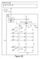
- FIG. 1is a block diagram illustrating an implementation of a data storage system 100 , in accordance with some embodiments. While some example features are illustrated, various other features have not been illustrated for the sake of brevity and so as not to obscure more pertinent aspects of the example implementations disclosed herein. To that end, as a non-limiting example, data storage system 100 includes storage device 120 (also sometimes called an information storage device, or a data storage device, or a memory device), which includes host interface 122 , storage controller 130 , and non-volatile memory (NVM) (e.g., one or more NVM device(s) 140 such as one or more flash memory devices), and is used in conjunction with computer system 110 .
- storage device 120also sometimes called an information storage device, or a data storage device, or a memory device
- NVMnon-volatile memory
- storage device 120includes a single NVM device while in other implementations storage device 120 includes a plurality of NVM devices.
- NVM devices 140include NAND-type flash memory or NOR-type flash memory.
- storage controller 130is a solid-state drive (SSD) controller.
- SSDsolid-state drive
- Computer system 110is coupled to storage device 120 through data connections 101 .
- computer system 110includes storage device 120 as a component and/or sub-system.
- Computer system 110may be any suitable computer device, such as a personal computer, a workstation, a computer server, or any other computing device.
- Computer system 110is sometimes called a host or host system.
- computer system 110includes one or more processors, one or more types of memory, optionally includes a display and/or other user interface components such as a keyboard, a touch screen display, a mouse, a track-pad, a digital camera and/or any number of supplemental devices to add functionality.
- computer system 110sends one or more host commands (e.g., read, write, and/or erase commands) on control line 111 to storage device 120 .
- host commandse.g., read, write, and/or erase commands
- computer system 110is a server system, such as a server system in a data center, and does not have a display and other user interface components.
- storage device 120includes NVM devices 140 such as flash memory devices (e.g., NVM devices 140 - 1 through 140 - n ) coupled to storage controller 130 .
- NVM controllerssometimes called memory channel controllers or port controllers
- storage controller 130includes a main storage controller for handling functions such as host command parsing and logical to physical address translation, and also includes a plurality of memory storage controllers for managing the NVM devices 140 in respective memory channels, including distributing individual memory operation (e.g. read, write, and erase) commands to the NVM device 140 .
- storage device 120includes M memory channels, each of which has an NVM controller and a set of NVM devices 140 coupled to the NVM controller, where M is an integer greater than one.
- Mis an integer greater than one.
- two or more memory channelsshare an NVM controller.
- each memory channelhas its own distinct set of NVM devices 140 .
- the number of memory channels in a typical storage deviceis 8, 16 or 32.
- the number of NVM devices 140 per memory channelis typically 8, 16, 32 or 64.
- the number of NVM devices 140is different in different memory channels.
- Storage controller 130is coupled to host interface 122 and NVM devices 140 .
- storage controller 130includes management module 132 for coordinating and executing commands corresponding to read, write and/or erase operations for reading data from, writing data to, or erasing data from a corresponding set of NVM devices 140 .
- management module 132receives data from computer system 110 through host interface 122
- management module 132sends data to computer system 110 through host interface 122 .
- management module 132receives an erase command from computer system 110 through host interface 122 .
- storage controller 130also conveys metadata, error correction information and/or other information in addition to data values to be stored in and data values read from NVM devices 140 .
- storage controller 130includes one or more processing units (e.g., processor(s) 134 , sometimes called CPUs or processors or microprocessors or microcontrollers) configured to execute instructions in one or more programs (e.g., stored in memory in storage controller 130 ).
- the one or more programsinclude, for example, instructions for determining an age metric for and accordingly adjusting configuration parameters associated with one or more, or a portion of, respective NVM devices 140 .
- one or more processor(s) 134are shared by one or more components within, and in some cases, beyond the function of storage controller 130 .
- Host interface 122also provides additional data, signals, voltages, and/or other information needed for communication between storage controller 130 and computer system 110 .
- storage controller 130 and host interface 122use a defined interface standard for communication, such as double data rate type three synchronous dynamic random access memory (DDR3).
- DDR3double data rate type three synchronous dynamic random access memory
- the defined interface standard for communication used by storage controller 130 and host interface 122is serial advance technology attachment (SATA).
- SATAserial advance technology attachment
- the defined interface standard for communication used by storage controller 130 and host interface 122is SAS (serial attached SCSI), or other storage interface.
- NVM devices 140each include a current measurement circuit 150 (e.g., 150 - 1 through 150 - n ) and optionally include one or more current registers 152 (e.g., 152 - 1 through 152 - n ).
- Current measurement circuit 150is used to measure a current drawn by one or more respective NVM devices 140 , or a portion thereof.
- the measured currentcorresponds to a current drawn during a memory operation (e.g., read, write, and/or erase operations), but in some circumstances (e.g., while an NVM device is power on, but not executing any commands) the measured current corresponds to a background/idle current drawn by a respective NVM device 140 .
- the measured currentis a current metric that corresponds to the current drawn by one or more NVM devices 104 , or a portion of a respective NVM device 140 .
- FIG. 1illustrates an embodiment in which current measurement circuit 150 is an internal component of NVM device 140 .
- current measurement circuit 150is sometimes external to NVM device 140 and is a separate component of, or alternatively a device external to, storage device 120 .
- Current measurement circuit 150is sometimes implemented using one or more current sensors and/or other passive or active components to measure electrical characteristics of storage device 120 and its components.
- storage controller 130retrieves current measurements (or alternatively, a drawn current metric associated with the current drawn) directly from current measurement circuit 150 , where the current measurements are used to determine an age metric for and accordingly adjust configuration parameters associated with one or more, or a portion of, respective NVM devices 140 .
- current measurements, or one or more characteristics of the current measurementsare stored in current register 152 of a respective NVM device 140 .
- storage controller 130retrieves the current measurements from current register 152 , as opposed to directly from current measurement circuit 150 .
- current register 152is external to NVM device 140 and is a separate component of storage device 120 .
- current register 152is a component of (e.g., FIG. 3C ), or optionally a component separate and distinct from (e.g., FIG. 3B ), current measurement circuit 150 .
- current register 152is implemented using high-speed random access memory, such as DRAM, SRAM, DDR RAM or other random access solid state memory devices, and/or non-volatile memory, such as one or more flash memory devices, other non-volatile solid state storage devices, magnetic disk storage devices, or optical disk storage devices.
- current register 152is implemented using one or more NVM devices distinct from NVM devices 140 , while in other implementations, current register 152 is implemented using a designated portion of NVM devices 140 .
- current register 152includes one or more logic gates, shift registers, clocks, flip flops, inverters, and/or other logic elements, where the foregoing elements are implemented with transistors and other active or passive electronic components.
- storage device 120is configured for enterprise storage suitable for applications such as cloud computing, or for caching data stored (or to be stored) in secondary storage, such as hard disk drives. In some other embodiments, storage device 120 is configured for relatively smaller-scale applications such as personal flash drives or hard-disk replacements for personal, laptop and tablet computers. Although flash memory devices and flash controllers are used as an example here, in some embodiments storage device 120 includes other non-volatile memory device(s) and corresponding non-volatile storage controller(s).
- storage device 120includes various additional features that have not been illustrated for the sake of brevity and so as not to obscure more pertinent features of the example implementations disclosed herein, and a different arrangement of features may be possible.
- Flash memory devicesutilize memory cells to store data as electrical values, such as electrical charges or voltages.
- Each flash memory celltypically includes a single transistor with a floating gate that is used to store a charge, which modifies the threshold voltage of the transistor (i.e., the voltage needed to turn the transistor on).
- the magnitude of the charge, and the corresponding threshold voltage the charge creates,is used to represent one or more data values.
- a reading threshold voltageis applied to the control gate of the transistor and the resulting sensed current or voltage is mapped to a data value.
- cell voltageand “memory cell voltage,” in the context of flash memory cells, means the threshold voltage of the memory cell, which is the minimum voltage that needs to be applied to the gate of the memory cell's transistor in order for the transistor to conduct current.
- reading threshold voltagessometimes also called reading signals and reading voltages
- gate voltagesapplied to the gates of the flash memory cells to determine whether the memory cells conduct current at that gate voltage.
- the raw data value for that read operationis a “1” and otherwise the raw data value is a “0.”
- FIG. 2is a block diagram illustrating an implementation of storage controller 130 , in accordance with some embodiments.
- storage controller 130includes NVM devices 140 - 1 through 140 - n , one or more processors 134 for executing modules, memory 200 , programs and/or instructions stored in memory 200 and thereby performing processing operations, host interface 122 , and one or more communication buses 202 for interconnecting these components.
- processors 134are instead performed by one or more processors of NVM controllers coupled between storage controller 130 and NVM devices 140 .
- NVM devices 140each include a current measurement circuit 150 (e.g., current measurement circuits 150 - 1 through 150 - n ) and an optional current register 152 (e.g., current registers 152 - 1 through 152 - n ), as described above with reference to FIG. 1 .
- Communication buses 202optionally include circuitry (sometimes called a chipset) that interconnects and controls communications between system components.
- Memory 200includes high-speed random access memory, such as DRAM, SRAM, DDR RAM or other random access solid state memory devices, and may include non-volatile memory, such as one or more magnetic disk storage devices, optical disk storage devices, flash memory devices, or other non-volatile solid state storage devices. Memory 200 optionally includes one or more storage devices remotely located from processor(s) 134 . Memory 200 , or alternately the non-volatile memory device(s) within memory 200 , comprises a non-transitory computer readable storage medium. In some embodiments, memory 200 , or the computer readable storage medium of memory 200 stores the following programs, modules, and data structures, or a subset thereof:
- memory 200or the computer readable storage medium of memory 200 further stores a configuration module for configuring storage controller 130 .
- the configuration moduleupon power up and upon reset, automatically sets the values of one or more configuration parameters of storage controller 130 in accordance with NVM devices 140 (e.g., the type of non-volatile memory) and/or characteristics of storage device 120 and/or data storage system 100 , which includes storage device 120 .
- NVM devices 140e.g., the type of non-volatile memory
- characteristics of storage device 120 and/or data storage system 100which includes storage device 120 .
- Each of the above identified elementsmay be stored in one or more of the previously mentioned memory devices, and corresponds to a set of instructions for performing a function described above.
- the above identified modules or programsi.e., sets of instructions
- memory 200may store a subset of the modules and data structures identified above.
- memory 200may store additional modules and data structures not described above.
- the programs, modules, and data structures stored in memory 200 , or the computer readable storage medium of memory 200provide instructions for implementing at least those portions of the methods described below with reference to FIGS. 5A-5C that are performed by components of storage device 120 .
- FIG. 2shows storage controller 130
- FIG. 2is intended more as a functional description of the various features which may be present in a storage controller than as a structural schematic of the embodiments described herein.
- items shown separatelycould be combined and some items could be separated.
- FIGS. 3A-3Dillustrate various implementations of a storage device, in accordance with some embodiments. While some example features and components are illustrated, various other features and components have not been illustrated for the sake of brevity and so as not to obscure more pertinent aspects of the example implementations disclosed herein. For instance, although not illustrated, some embodiments of storage device 120 include multiple current measurement circuits, optional current registers, and NVM devices (e.g., NVM devices 140 - 1 through 140 - n ), where each NVM device has a respective set of memory elements, bit lines, word lines.
- NVM devices 140 - 1 through 140 - ne.g., NVM devices 140 - 1 through 140 - n
- FIG. 3Ais a block diagram illustrating an implementation of a storage device with current measurement circuits internal to a non-volatile memory device, in accordance with some embodiments.
- storage device 120includes NVM devices 140 (each of which includes a set of memory elements 302 for each bit line 306 ), storage controller 130 , bit lines 306 , word lines 304 , current measurement circuits 308 , and one or more connections 300 .
- NVM devices 140each of which includes a set of memory elements 302 for each bit line 306
- storage controller 130includes NVM devices 140 (each of which includes a set of memory elements 302 for each bit line 306 ), storage controller 130 , bit lines 306 , word lines 304 , current measurement circuits 308 , and one or more connections 300 .
- a current drawn by bit lines 306is measured by current measurement circuits 308 and accessed by storage controller 130 directly through current read lines 310 .
- Storage controller 130determines an age metric based on age criteria, and if the
- NVM device 140is configured as a memory array composed of multiple strings of memory, where each string is composed of multiple memory elements (e.g., 302 - 0 through 302 -N) connected in series, sharing a single bit line (e.g., 306 - 0 ), and accessed as a group.
- storage controller 130sends signals corresponding to write and/or erase operations to one or more memory elements (e.g., 302 - 0 through 302 -N) through write lines (e.g., 304 - 0 through 304 -N).
- memory elements 302are coupled to storage controller 130 through one or more connections 300 , where connections 300 include write lines 304 .
- each NVM device 140includes multiple individually addressable blocks (e.g., erase blocks) having predefined storage capacities, where in some embodiments, each block includes multiple individually addressable pages.
- a combination of memory elements 302 within a respective NVM device 140may comprise one or more blocks and/or pages.
- an NVM device 140 having 512 megabytes of storage capacityincludes multiple 128 kilobyte blocks, where each block includes multiple 4 kilobyte pages.
- a current measurement circuit(e.g., 308 - 0 ) is coupled between a respective bit line (e.g., 306 - 0 ) and a respective set of memory elements (e.g., 302 - 0 through 302 -N).
- FIG. 3Aillustrates one implementation in which current measurement circuits 308 are internal components of NVM device 140 - n .
- current measurement circuits 308 - 0 through 308 -Mare collectively referred to as current measurement circuit 150 - n of NVM device 140 - n . As illustrated in FIG.
- NVM device 140includes a single current measurement circuit 308 positioned within the device (e.g., between a voltage source and the device's array of memory cells) so as to measure all current drawn by the entire array of memory cells in the device.
- current measurement circuits 308each measure a current through a respective bit line (e.g., 306 - 0 ), corresponding to a current drawn during a memory operation by a respective set of memory elements connected in series and sharing the respective bit line (e.g., memory elements 302 - 0 through 302 -N, sharing bit line 306 - 0 .
- a current measurement circuit 308measures a current drawn by one or more blocks, or one or more pages of an NVM device.
- a current drawn by a particular NVM devicee.g., 140 - n
- an array of NVM devicese.g., NVM devices 140 - 1 through 140 - n
- a current drawn by entire NVM device 140 - nis determined by summing the current measurements of current measurement circuits 308 - 0 through 308 -M.
- a single current measurement circuit 308 located within NVM device 140measures current drawn by an entire NVM device 140 , or by all memory cells in NVM device 140 .
- storage controller 130retrieves current measurements (or alternatively, a drawn current metric associated with the current drawn) directly from current measurement circuits 308 through current read lines 310 . Further discussion regarding determining an age metric for and accordingly adjusting configuration parameters associated with at least a portion of NVM device 140 - n is provided below with respect to FIGS. 5A-5C .
- FIG. 3Bis a block diagram illustrating an alternative implementation of a storage device with current measurement circuits and a current register internal to a non-volatile memory device, in accordance with some embodiments.
- the alternative implementation of storage device 120 illustrated in FIG. 3Bcontains similar features to the implementation of FIG. 3A (see above for further discussion regarding the features and components of storage device 120 ). However, the alternative implementation of FIG. 3B additionally includes a current register (e.g., 152 - n ), internal to a respective NVM device (e.g., 140 - n ), to which current measurement circuits 308 are coupled through current read lines 310 . As described above with respect to FIG. 1 , current register 152 stores current measurements taken by current measurement circuits 308 .
- a current registere.g., 152 - n
- storage controller 130retrieves current measurements from current register 152 - n , as opposed to each of current measurement circuits 308 .
- a respective current register 152may determine a current drawn by a particular NVM device (e.g., 140 - n ) by summing the current measurements of the respective current measurement circuits 308 .
- a current drawn by an array of NVM devicese.g., 140 - 1 through 140 - n
- a single current measurement circuit 308 located within NVM device 140measures current drawn by an entire NVM device 140 - n , or by all memory cells in NVM device 140 .
- current measurement circuit 308is positioned between an internal voltage source, labeled V DD , and the NVM device's memory array. Further, in the example shown in FIG. 3C , current measurement circuit 308 is positioned between internal voltage source V DD and the NVM device's memory operation circuitry 320 - n .
- memory operation circuitry 320 - nincludes voltage regulator and boost circuitry for generating internal voltages, sense amplifiers for reading data from memory cells, and control logic for performing read, write and erase operations.
- the control logicmay also control when current measurements are taken by current measurement circuit 308 .
- one or more current measurements made by current measurement circuit 308are stored in current register 152 - n , from where they are read by controller 130 .
- FIG. 3Dis a block diagram illustrating another alternative implementation of a storage device with a current measurement circuit 322 - n external to a non-volatile memory device 140 - n , in accordance with some embodiments.
- the external current measurement circuit 322 - nincludes a current sensor 324 and optionally includes a current register 326 - n , in accordance with some embodiments.
- storage device 120 illustrated in FIG. 3Dcontains similar features to the implementation of FIG. 3C (see above for further discussion regarding the features and components of storage device 120 ).
- the alternative implementation of FIG. 3Dincludes a current measurement circuit 322 - n external to NVM device 140 - n , coupled between storage controller 130 and NVM device 140 - n .
- storage device 120includes multiple measurement circuits 322 external to a respective NVM device 140 - n for measuring current drawn by multiple distinct portions of NVM device 140 - 1 . These implementations enable the use of external current measurement devices without needing to incorporate current measurement circuitry within NVM devices 140 .
- storage controller 130retrieves current measurements directly from current measurement circuit 322 - n , or optionally, from current register 326 - n .
- a respective current register 326determines a current drawn by a particular NVM device (e.g., 140 - n ) by summing the current measurements of multiple current measurement circuits 324 .
- a current drawn by an array of NVM devicese.g., NVM devices 140 - 1 through 140 - n ) is determined by summing the current measurements retrieved from current registers 326 - 0 through 326 - n.
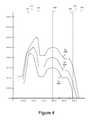
- FIG. 4is a prophetic illustration of a continuous time-domain plot of current drawn for a bit line of distinct non-volatile memory devices during an erase operation, in accordance with some embodiments.
- each of current measurements I D1 , I D2 , and I D3corresponds to a current drawn by at least a portion of a respective NVM device (e.g., I D1 corresponds to the current measured on bit line 306 - 0 of NVM device 140 - 1 ) during an erase operation or erase verify operation.
- each respective NVM devicehas a distinct program-erase (PE) cycle count.
- PEprogram-erase
- current measurements I D1 , I D2 , and I D3correspond to the current drawn by NVM devices 140 - 1 through 140 - 3 , having PE cycle counts of 1000, 1500, and 2000, respectively.
- An age metricis representative of the level of wear and the overall endurance of an NVM device, which, in some embodiments, is represented by a PE cycle count of the NVM device. Determining an age metric for at least the portion of an NVM device is based on age criteria, where the age criteria includes a characteristic of a measured current.
- FIG. 4illustrates exemplary characteristics of a measured current.
- the characteristic of the measured currente.g., I D1
- the characteristic of the measured currentis the total current drawn by at least a portion of a respective NVM device (e.g., 140 - 1 ) over the duration of a sampling window.
- the total current drawn by the NVM device corresponding to current measurement I D1e.g., 140 - 1
- the total current drawn by the NVM device corresponding to current measurement I D1is larger than the total current drawn by the NVM device corresponding to current measurement I D2 (e.g., 140 - 1 ).
- NVM device 140 - 1has a lower PE cycle count (1000) than NVM device 140 - 2 (1500)
- an age metric based on a larger total current drawnwill be less than an age metric based on a smaller total current drawn.
- NVM device 140 - 1will have a smaller age metric compared to NVM device 140 - 2 .
- the characteristic of the measured currentis a peak current drawn by at least a portion of a respective NVM device (e.g., 140 - 1 ) over the duration of a sampling window.
- a respective NVM devicee.g., 140 - 1
- the peak current drawn by the NVM device corresponding to current measurement I D1e.g., 410 , NVM device 140 - 1
- the peak current drawn by the NVM device corresponding to current measurement I D2e.g., 412 , 140 - 2 .
- NVM device 140 - 1has a lower PE cycle count (1000) than NVM device 140 - 2 (1500)
- an age metric based on a larger peak currentwill be less than an age metric based on a smaller peak current.
- NVM device 140 - 1will have a smaller age metric compared to NVM device 140 - 2 .
- the characteristic of the measured currentis a peak current drawn by at least a portion of a respective NVM device (e.g., 140 - 1 ) over the duration of a sampling window, specifically over the duration of an erase verify operation.
- a respective NVM devicee.g., 140 - 1
- the duration between approximately 1052 microseconds and 1064 microsecondscorresponds to the duration of an erase verify operation executed for NVM devices 140 - 1 through 140 - 3 (e.g., corresponding to current measurements I D1 , I D2 , and I D3 , respectively).
- the peak current drawn by the NVM device 140 - 1e.g., approx.
- NVM device 140 - 1has a lower PE cycle count (1000) than NVM device 140 - 2 (1500)
- an age metric based on peak current during an erase verify operationis inversely related to the peak current during the erase verify operation.
- NVM device 140 - 1will have a smaller age metric compared to NVM device 140 - 2 .
- the characteristic of the measured currentis a timing of a current event (e.g., how quickly the current increases above and/or falls below a predefined current level during the execution of a memory operation).
- a rising current threshold levelis defined as 0.020 amps
- I D1corresponding to NVM device 140 - 1
- I D2corresponding to NVM device 140 - 2
- NVM device 140 - 1has a lower PE cycle count (1000) than NVM device 140 - 2 (1500)
- an age metric based on a current that increases above a predefined current threshold level more quicklywill be less than an age metric based on a current that increases above a predefined current threshold level less quickly.
- NVM device 140 - 1will have a smaller age metric compared to NVM device 140 - 2 .
- a falling current threshold levelis defined as 0 A
- I D1falls (e.g., at time 420 ) to the falling current threshold level later than I D2 (e.g., 422 ).
- NVM device 140 - 1has a lower PE cycle count (1000) than NVM device 140 - 2 (1500)
- an age metric based on a current that falls to (or below) a predefined current threshold level less quicklywill be less than an age metric based on a current that falls below a predefined current level more quickly.
- NVM device 140 - 1will have a smaller age metric compared to NVM device 140 - 2 .
- FIGS. 5A-5Cillustrate a flowchart representation of a method 500 of determining an age metric for and accordingly adjusting configuration parameters associated with a non-volatile memory device, in accordance with some embodiments.
- a non-volatile memory systeme.g., storage device 120 , FIG. 1
- which includes a plurality of non-volatile memory devicese.g., 140 - 1 through 140 - n
- a non-volatile memory systemexecutes ( 502 ) a memory operation with respect to a portion of a non-volatile memory device.
- the memory operationis selected ( 504 ) from a group consisting of: a read operation ( 506 ), a write operation ( 508 ), and an erase operation ( 510 ).
- an erase operationcomprises a plurality of erase loops.
- the portion of the non-volatile memory devicecomprises a single erase block ( 512 ).
- Portions of an NVM device 140e.g., multiple memory elements 302 connected in series, or a subset thereof are described in greater detail above with respect to FIGS. 3A-3D .
- a current corresponding to current drawn by at least the portion of the non-volatile memory deviceis measured ( 514 ) during the memory operation.
- the current drawnis by an entire NVM device (e.g., 140 - n , FIG. 3A ), or optionally, an array of NVM devices (e.g., 140 - 1 through 140 - n ).
- the currentis measured ( 516 ) for the duration of a sampling window.
- a current measurement circuite.g., 308 - 0 , FIG. 3A
- the duration of the sampling windowcomprises ( 518 ) the duration of the memory operation.
- a current measurement circuite.g., 308 - 0 , FIG. 3A ) measures the current drawn by a portion of an NVM device (e.g., memory elements 302 - 0 through 302 -N) for the duration of an erase operation lasting, for example, 1200 microseconds.
- measuring the currentis from a physical location internal to the non-volatile memory device. Additionally and/or alternatively, measuring the current is from a physical location external to the non-volatile memory device. Various embodiments for locations at which a current is measured (and thus, where current measurement circuits 150 are implemented) are described in greater detail with respect to FIGS. 3A-3D .
- measuring the currentincludes measuring the current drawn across one or more bit lines corresponding to the portion of the non-volatile memory device. As described above with respect to FIGS. 3A-3D , in some implementations, measuring the current includes measuring the current drawn by a respective set of memory elements connected in series and sharing the respective bit line (e.g., memory elements 302 - 0 through 302 -N sharing bit line 308 - 0 , FIG. 3A ).
- measuring the current ( 526 )is in accordance with a current measurement profile, wherein the current measurement profile is based on a type of the non-volatile memory device.
- Types of the NVM devicesinclude, for example, planar NAND, 3D (BiCS) NAND, and ReRAM.
- An age metricis determined ( 528 ) for at least the portion of the non-volatile memory device based on age criteria including a characteristic of the measured current.
- the characteristic of the measured currentis a total current drawn ( 520 ) by the portion of the non-volatile memory device over the duration of the sampling window.
- FIG. 4describes in greater detail other exemplary characteristics of the measured current (e.g., a peak current drawn, a timing of a current event, etc.).
- the age metricis determined ( 530 ) based on age criteria further including one or more selected from the group consisting of: a program-erase (PE) cycle count ( 532 ) corresponding to a number of PE cycles performed on the portion of the non-volatile memory device; a number of erase loops ( 534 ) required for successfully executing the memory operation, wherein the memory operation is an erase operation; and a measured bit error rate (BER) ( 536 ) of the portion of the non-volatile memory device.
- PEprogram-erase
- BERbit error rate
- the determined age metric for NVM device 140 - 1having a PE cycle count of 2500 and having drawn 0.5 milliamps of current during a 40 microseconds erase operation, will typically be higher than the determined age metric for NVM device 140 - 1 , having a PE cycle count of 1000 and having drawn 1.0 milliamps of current during the same 40 microseconds erase operation, where a greater age metric corresponds to greater physical wear of an NVM device.
- an NVM device requiring a greater number of erase loops to successfully complete erasure of one or more blocks during an erase operationwill typically have a greater age metric than an NVM device requiring fewer erase loops, where a greater age metric corresponds to greater physical wear of an NVM device.
- an NVM device with a greater BER than another NVM devicewill typically have a greater age metric, where a greater age metric corresponds to greater physical wear of an NVM device.
- the age metricis determined irrespective of the BER.
- An age metricdetermined irrespective of the BER, reduces the amount of time for determining the overall endurance of an NVM device.
- the BER approachfirst requires programming a completely erased block and subsequently detecting an error in the programming, which is a lengthier process than determining an age metric based on age criteria that include a characteristic of a measured current.
- the measured currentis measured during performance a memory operation that is performed irrespective of the age measurement process, for example, during performance of a memory operation that is performed in response to a read or write command from a host computer, or in response to a block erase command issued by a garbage collection process.
- the age metricis determined with an algorithm that is defined as a function of one or more age criteria. Furthermore, in some implementations, each of the one or more age criteria used in the algorithm have a respective predefined weight.
- I totalis the total current drawn by an NVM device (e.g., 140 - n ) for the duration of a memory operation (e.g., erase operation)
- PEis the program-erase count of the NVM device
- X and Yare the predefined weights of I total and PE, respectively.
- one or more configuration parameters associated with at least the portion of the non-volatile memory deviceare adjusted ( 538 ).
- the one or more predefined threshold criteriacorrespond to the age metric of a new or moderately worn NVM device (e.g., PE cycle count of 500, 1.5 milliamps of total current drawn).
- a predefined threshold criterionis satisfied if the age metric of an NVM device is a predefined percentage (e.g., 10%) above the age metric corresponding to the predefined threshold criteria.
- one or more configuration parameters associated with a specific portion of the NVM devicee.g., bit line 306 - 0 of NVM device 140 - n , shared by memory elements 302 in FIG. 3A ; or, in another example, specific erase blocks of NVM device 140 - n ) are adjusted.
- the one or more adjusted configuration parametersinclude ( 540 ) at least one of: a programming parameter ( 542 ), a storage density of the non-volatile memory device or the portion of the non-volatile memory device ( 544 ), an error correction code (ECC) strength ( 546 ), and a wear leveling setting ( 548 ).
- programming parametersinclude one or more write voltages (starting voltage, and optionally voltage step size), a maximum number of programming pulses, and optionally a length of the programming pulses.
- NVM device 140 - nexceeds a predefined threshold (e.g., NVM device 140 - n has an age metric greater than that of an NVM device having a PE cycle count of 1500)
- storage controller 130applies a greater write voltage to memory elements 302 through write lines 304 to better ensure successful programming of data to the memory elements.
- an NVM devicee.g., an NVM device having multi-level cell (MLC) memory elements
- MLCmulti-level cell
- some or all of the MLC memory elements of the NVM deviceare recharacterized (sometimes called reconfigured) for use at a lower storage density than the storage density previously used (e.g., storage density is reduced from X3 to X2).
- a stronger ECCis used (e.g., using LDPC over BCH).
- a wear leveling settingis adjusted such that storage controller 130 programs and erases blocks of NVM device 140 - n less frequently than other NVM devices of an array (e.g., NVM devices 140 - 1 and 140 - 2 ) having age metrics that do not exceed the predefined threshold criteria.
- the non-volatile memory deviceincludes (550) one or more three-dimensional (3D) memory devices and circuitry associated with operation of memory elements in the one or more 3D memory devices. Furthermore, in some implementations, the circuitry and one or more memory elements in a respective 3D memory device, of the one or more 3D memory devices, are on the same substrate ( 552 ).
- At least the characteristic of the measured currentis stored (556) in a register.
- Current registersare described in greater detail above with respect to FIG. 1 .
- the storage deviceincludes (1) an interface for coupling the storage device to a host system, (2) a plurality of non-volatile memory controllers, each controller of the plurality of controllers configured to manage execution of commands in one or more command queues managed by controller, and (3) a plurality of distinct sets of non-volatile memory devices, each controlled by a corresponding one of the non-volatile memory controllers.
- Semiconductor memory devicesinclude volatile memory devices, such as dynamic random access memory (“DRAM”) or static random access memory (“SRAM”) devices, non-volatile memory devices, such as resistive random access memory (“ReRAM”), electrically erasable programmable read only memory (“EEPROM”), flash memory (which can also be considered a subset of EEPROM), ferroelectric random access memory (“FRAM”), and magnetoresistive random access memory (“MRAM”), and other semiconductor elements capable of storing information.
- volatile memory devicessuch as dynamic random access memory (“DRAM”) or static random access memory (“SRAM”) devices
- non-volatile memory devicessuch as resistive random access memory (“ReRAM”), electrically erasable programmable read only memory (“EEPROM”), flash memory (which can also be considered a subset of EEPROM), ferroelectric random access memory (“FRAM”), and magnetoresistive random access memory (“MRAM”), and other semiconductor elements capable of storing information.
- ReRAMresistive random access memory
- EEPROMelectrically erasable
- the memory devicescan be formed from passive and/or active elements, in any combinations.
- passive semiconductor memory elementsinclude ReRAM device elements, which in some embodiments include a resistivity switching storage element, such as an anti-fuse, phase change material, etc., and optionally a steering element, such as a diode, etc.
- active semiconductor memory elementsinclude EEPROM and flash memory device elements, which in some embodiments include elements containing a charge storage region, such as a floating gate, conductive nanoparticles, or a charge storage dielectric material.
- Multiple memory elementsmay be configured so that they are connected in series or so that each element is individually accessible.
- flash memory devices in a NAND configurationtypically contain memory elements connected in series.
- a NAND memory arraymay be configured so that the array is composed of multiple strings of memory in which a string is composed of multiple memory elements sharing a single bit line and accessed as a group.
- memory elementsmay be configured so that each element is individually accessible (e.g., a NOR memory array).
- NAND and NOR memory configurationsare exemplary, and memory elements may be otherwise configured.
- the semiconductor memory elements located within and/or over a substratemay be arranged in two or three dimensions, such as a two dimensional memory structure or a three dimensional memory structure.
- the semiconductor memory elementsare arranged in a single plane or a single memory device level.
- memory elementsare arranged in a plane (e.g., in an x-z direction plane) which extends substantially parallel to a major surface of a substrate that supports the memory elements.
- the substratemay be a wafer over or in which the layer of the memory elements are formed or it may be a carrier substrate which is attached to the memory elements after they are formed.
- the substratemay include a semiconductor such as silicon.
- the memory elementsmay be arranged in the single memory device level in an ordered array, such as in a plurality of rows and/or columns. However, the memory elements may be arrayed in non-regular or non-orthogonal configurations.
- the memory elementsmay each have two or more electrodes or contact lines, such as bit lines and word lines.
- a three dimensional memory arrayis arranged so that memory elements occupy multiple planes or multiple memory device levels, thereby forming a structure in three dimensions (i.e., in the x, y and z directions, where the y direction is substantially perpendicular and the x and z directions are substantially parallel to the major surface of the substrate).
- a three dimensional memory structuremay be vertically arranged as a stack of multiple two dimensional memory device levels.
- a three dimensional memory arraymay be arranged as multiple vertical columns (e.g., columns extending substantially perpendicular to the major surface of the substrate, i.e., in the y direction) with each column having multiple memory elements in each column.
- the columnsmay be arranged in a two dimensional configuration (e.g., in an x-z plane), resulting in a three dimensional arrangement of memory elements with elements on multiple vertically stacked memory planes.
- Other configurations of memory elements in three dimensionscan also constitute a three dimensional memory array.
- the memory elementsmay be coupled together to form a NAND string within a single horizontal (e.g., x-z) memory device level.
- the memory elementsmay be coupled together to form a vertical NAND string that traverses across multiple horizontal memory device levels.
- Other three dimensional configurationscan be envisioned wherein some NAND strings contain memory elements in a single memory level while other strings contain memory elements which span through multiple memory levels.
- Three dimensional memory arraysmay also be designed in a NOR configuration and in a ReRAM configuration.
- a monolithic three dimensional memory arraytypically, one or more memory device levels are formed above a single substrate.
- the monolithic three dimensional memory arraymay also have one or more memory layers at least partially within the single substrate.
- the substratemay include a semiconductor such as silicon.
- the layers constituting each memory device level of the arrayare typically formed on the layers of the underlying memory device levels of the array.
- layers of adjacent memory device levels of a monolithic three dimensional memory arraymay be shared or have intervening layers between memory device levels.
- non-monolithic stacked memoriescan be constructed by forming memory levels on separate substrates and then stacking the memory levels atop each other. The substrates may be thinned or removed from the memory device levels before stacking, but as the memory device levels are initially formed over separate substrates, the resulting memory arrays are not monolithic three dimensional memory arrays. Further, multiple two dimensional memory arrays or three dimensional memory arrays (monolithic or non-monolithic) may be formed on separate chips and then packaged together to form a stacked-chip memory device.
- Associated circuitryis typically required for operation of the memory elements and for communication with the memory elements.
- memory devicesmay have circuitry used for controlling and driving memory elements to accomplish functions such as programming and reading.
- This associated circuitrymay be on the same substrate as the memory elements and/or on a separate substrate.
- a controller for memory read-write operationsmay be located on a separate controller chip and/or on the same substrate as the memory elements.
- three-dimensional memory device(or 3D memory device) is herein defined to mean a memory device having multiple memory layers or multiple levels (e.g., sometimes called multiple memory device levels) of memory elements, including any of the following: a memory device having a monolithic or non-monolithic 3D memory array, some non-limiting examples of which are described above; or two or more 2D and/or 3D memory devices, packaged together to form a stacked-chip memory device, some non-limiting examples of which are described above.
- firstfirst
- secondsecond
- first contactfirst contact
- first contactsecond contact
- first contactsecond contact
- the term “if”may be construed to mean “when” or “upon” or “in response to determining” or “in accordance with a determination” or “in response to detecting,” that a stated condition precedent is true, depending on the context.
- the phrase “if it is determined [that a stated condition precedent is true]” or “if [a stated condition precedent is true]” or “when [a stated condition precedent is true]”may be construed to mean “upon determining” or “in response to determining” or “in accordance with a determination” or “upon detecting” or “in response to detecting” that the stated condition precedent is true, depending on the context.
Landscapes
- Engineering & Computer Science (AREA)
- Theoretical Computer Science (AREA)
- Physics & Mathematics (AREA)
- General Engineering & Computer Science (AREA)
- Quality & Reliability (AREA)
- General Physics & Mathematics (AREA)
- Computing Systems (AREA)
- Mathematical Physics (AREA)
- Computer Hardware Design (AREA)
- Techniques For Improving Reliability Of Storages (AREA)
- Read Only Memory (AREA)
Abstract
Description
memory operation module 210, which dispatches commands corresponding to read, write and/or erase operations for reading data from, writing data to, or erasing data fromNVM devices 140; in some implementationsmemory operation module 210 dispatches commands to memory channel controllers, which in turn dispatch the commands toNVM devices 140.current measure module 212, which retrieves current measurements or metrics from thecurrent measurement circuits 150 orcurrent registers 152 of theNVM devices 140; in some implementationscurrent measure module 212 instructs thecurrent measurement circuits 150 inNVM devices 140 to measure the current drawn by those devices or by particular portions of those devices; additionally, in some implementations,current measure module 212 manages when, for how long, and how frequently current measurements are taken;- current measure table214, which stores current measurements (or current metrics corresponding to current drawn) received from
current measurement circuits 150 orcurrent registers 152 ofNVM devices 140; - age
metric module 216, which determines age metrics, based on defined age criteria, forNVM devices 140 or for respective portions ofNVM devices 140; - current
characteristic module 218, which determines one or more characteristics (e.g., magnitude of an observed peak current, total current drawn, etc.) of a current measured bycurrent measurement circuit 150, and identifies a value for each determined characteristic; - Program-erase (PE)
cycle count module 220, which determines, with respect to eachNVM device 140 of a plurality of NVM devices, a current PE cycle count for theNVM device 140 or for respective portions (e.g., erase blocks) of theNVM device 140; - Bit Error Rate (BER)
module 222, which executes a sequence of commands to determine, with respect to aparticular NVM device 140 of the NVM devices instorage device 120, a BER of theNVM device 140 or of respective portions of theNVM device 140; in some embodiments, the sequence of commands includes erasing portions of anNVM device 140, programming a correctable data pattern into the erased portions, and reading data from the programmed portions to calculate a BER; - erase
loop module 224, which determines a number of erase loops required for successfully executing an erase operation on a specified portion of aparticular NVM device 140; - current
measure profile module 226, which instructscurrent measurement circuit 150 to measure a current drawn or a characteristic (e.g., a timing characteristic or peak current) of the current drawn in accordance with a current measurement profile, which is optionally based on the type of the NVM device; threshold criteria module 228, which determines whether an age metric of aparticular NVM device 140 or portion ofNVM device 140 satisfies a predefined threshold criteria (e.g., determining whether an age metric corresponding to the magnitude of a peak current during a particular type of memory operation is at least X % less than the magnitude of the peak current during that type of memory operation for (A) the same device when the device was new, or (B) a new device);- age metric table230, which stores previous and new values determined and/or calculated by age
metric module 216 and its sub-modules (e.g., age metric values, PE cycle counts, BER values, etc.); - configuration adjustment module232, which, in accordance with a determination (by threshold criteria module228) that an age metric satisfies one or more predefined threshold criteria, determines which configuration parameters associated with
NVM device 140, or a portion ofNVM device 140, (e.g., programming parameters, storage density, etc.) to adjust; - programming module234, which adjusts one or more programming parameters (e.g., threshold write voltage) of
NVM device 140, or a portion ofNVM device 140; - storage density module236, which adjusts the storage density (e.g., three bits per cell to two bits per cell) of the memory cells of
NVM device 140, or a portion ofNVM device 140; - Error Correction Code (ECC)
module 238, which adjusts the strength of the ECC used for detecting and correcting errors in data written to and read fromNVM device 140, or a portion ofNVM device 140; - optionally, wear leveling
module 240, which adjusts one or more configuration settings related to the wear leveling scheme applied to specific portions of NVM device140 (e.g., instructingstorage controller 130 to write less frequently to blocks with greater wear, based on the determined age metric); and - configuration table242, which stores previous and adjusted values of the various configuration parameters (e.g., programming parameters, storage density, etc.) corresponding to the sub-modules of configuration adjustment module232.
(AgeMetric)NVM−n=X*(Itotal)+Y*(PE),
Claims (27)
Priority Applications (1)
| Application Number | Priority Date | Filing Date | Title |
|---|---|---|---|
| US14/298,854US9070481B1 (en) | 2014-05-30 | 2014-06-06 | Internal current measurement for age measurements |
Applications Claiming Priority (2)
| Application Number | Priority Date | Filing Date | Title |
|---|---|---|---|
| US201462005975P | 2014-05-30 | 2014-05-30 | |
| US14/298,854US9070481B1 (en) | 2014-05-30 | 2014-06-06 | Internal current measurement for age measurements |
Publications (1)
| Publication Number | Publication Date |
|---|---|
| US9070481B1true US9070481B1 (en) | 2015-06-30 |
Family
ID=53441836
Family Applications (1)
| Application Number | Title | Priority Date | Filing Date |
|---|---|---|---|
| US14/298,854Expired - Fee RelatedUS9070481B1 (en) | 2014-05-30 | 2014-06-06 | Internal current measurement for age measurements |
Country Status (1)
| Country | Link |
|---|---|
| US (1) | US9070481B1 (en) |
Cited By (19)
| Publication number | Priority date | Publication date | Assignee | Title |
|---|---|---|---|---|
| US9514845B1 (en)* | 2013-12-12 | 2016-12-06 | SK Hynix Inc. | Check after write for assessing wear related degradation in solid state storage |
| US9786374B2 (en)* | 2015-03-19 | 2017-10-10 | SK Hynix Inc. | Nonvolatile memory device, operating method thereof, and test system for optimizing erase loop operations |
| US9947401B1 (en)* | 2016-12-22 | 2018-04-17 | Sandisk Technologies Llc | Peak current management in non-volatile storage |
| US10241859B2 (en)* | 2015-07-23 | 2019-03-26 | Toshiba Memory Corporation | Memory system and method of controlling nonvolatile memory |
| US10297611B1 (en) | 2017-12-27 | 2019-05-21 | Micron Technology, Inc. | Transistors and arrays of elevationally-extending strings of memory cells |
| US20190278679A1 (en)* | 2018-03-08 | 2019-09-12 | Symbol Technologies, Llc | Method, system and apparatus for assessing application impact on memory devices |
| US10446681B2 (en)* | 2017-07-10 | 2019-10-15 | Micron Technology, Inc. | NAND memory arrays, and devices comprising semiconductor channel material and nitrogen |
| US10559466B2 (en) | 2017-12-27 | 2020-02-11 | Micron Technology, Inc. | Methods of forming a channel region of a transistor and methods used in forming a memory array |
| US10720202B2 (en)* | 2018-08-21 | 2020-07-21 | Fujitsu Limited | Apparatus for memory control |
| US10719243B2 (en) | 2018-05-30 | 2020-07-21 | Apple Inc. | Techniques for preserving an expected lifespan of a non-volatile memory |
| WO2021015813A1 (en)* | 2019-07-19 | 2021-01-28 | Silicon Storage Technology, Inc. | Testing circuitry and methods for analog neural memory in artificial neural network |
| CN112997254A (en)* | 2018-10-12 | 2021-06-18 | 美光科技公司 | Metric-based reactive reads for screening defect-prone memory blocks |
| US11127476B2 (en)* | 2019-09-13 | 2021-09-21 | Kioxia Corporation | Memory system controlling a threshold voltage in a read operation and method |
| US11393546B2 (en) | 2019-07-19 | 2022-07-19 | Silicon Storage Technology, Inc. | Testing circuitry and methods for analog neural memory in artificial neural network |
| US11514981B1 (en)* | 2021-06-04 | 2022-11-29 | International Business Machines Corporation | Programming devices and weights in hardware |
| US20220405003A1 (en)* | 2021-06-17 | 2022-12-22 | Seagate Technology Llc | Balancing power, endurance and latency in a ferroelectric memory |
| US11538919B2 (en) | 2021-02-23 | 2022-12-27 | Micron Technology, Inc. | Transistors and arrays of elevationally-extending strings of memory cells |
| US11550737B2 (en)* | 2019-07-31 | 2023-01-10 | Micron Technology, Inc. | Adjusting characteristic of system based on profile |
| US20250173088A1 (en)* | 2023-11-27 | 2025-05-29 | Western Digital Technologies, Inc. | Non-volatile memory with operation adjustment based on open block ratio and cycling |
Citations (240)
| Publication number | Priority date | Publication date | Assignee | Title |
|---|---|---|---|---|
| US4916652A (en) | 1987-09-30 | 1990-04-10 | International Business Machines Corporation | Dynamic multiple instruction stream multiple data multiple pipeline apparatus for floating-point single instruction stream single data architectures |
| US5270979A (en) | 1991-03-15 | 1993-12-14 | Sundisk Corporation | Method for optimum erasing of EEPROM |
| US5519847A (en) | 1993-06-30 | 1996-05-21 | Intel Corporation | Method of pipelining sequential writes in a flash memory |
| US5530705A (en) | 1995-02-08 | 1996-06-25 | International Business Machines Corporation | Soft error recovery system and method |
| US5537555A (en) | 1993-03-22 | 1996-07-16 | Compaq Computer Corporation | Fully pipelined and highly concurrent memory controller |
| US5551003A (en) | 1992-12-11 | 1996-08-27 | International Business Machines Corporation | System for managing log structured array (LSA) of DASDS by managing segment space availability and reclaiming regions of segments using garbage collection procedure |
| US5657332A (en) | 1992-05-20 | 1997-08-12 | Sandisk Corporation | Soft errors handling in EEPROM devices |
| US5666114A (en) | 1994-11-22 | 1997-09-09 | International Business Machines Corporation | Method and means for managing linear mapped address spaces storing compressed data at the storage subsystem control unit or device level |
| US5708849A (en) | 1994-01-26 | 1998-01-13 | Intel Corporation | Implementing scatter/gather operations in a direct memory access device on a personal computer |
| US5765185A (en) | 1995-03-17 | 1998-06-09 | Atmel Corporation | EEPROM array with flash-like core having ECC or a write cache or interruptible load cycles |
| US5943692A (en) | 1997-04-30 | 1999-08-24 | International Business Machines Corporation | Mobile client computer system with flash memory management utilizing a virtual address map and variable length data |
| US5982664A (en) | 1997-10-22 | 1999-11-09 | Oki Electric Industry Co., Ltd. | Semiconductor memory capable of writing and reading data |
| US6000006A (en) | 1997-08-25 | 1999-12-07 | Bit Microsystems, Inc. | Unified re-map and cache-index table with dual write-counters for wear-leveling of non-volatile flash RAM mass storage |
| US6006345A (en) | 1997-05-09 | 1999-12-21 | International Business Machines Corporation | Pattern generator for memory burn-in and test |
| US6016560A (en) | 1995-06-14 | 2000-01-18 | Hitachi, Ltd. | Semiconductor memory, memory device, and memory card |
| US6018304A (en) | 1997-12-18 | 2000-01-25 | Texas Instruments Incorporated | Method and apparatus for high-rate n/n+1 low-complexity modulation codes with adjustable codeword length and error control capability |
| US6070074A (en) | 1998-04-24 | 2000-05-30 | Trw Inc. | Method for enhancing the performance of a regenerative satellite communications system |
| US6138261A (en) | 1998-04-29 | 2000-10-24 | Trw Inc. | Concatenated coding system for satellite communications |
| US6182264B1 (en) | 1998-05-22 | 2001-01-30 | Vlsi Technology, Inc. | Smart dynamic selection of error correction methods for DECT based data services |
| US6192092B1 (en) | 1998-06-15 | 2001-02-20 | Intel Corp. | Method and apparatus for clock skew compensation |
| US6295592B1 (en) | 1998-07-31 | 2001-09-25 | Micron Technology, Inc. | Method of processing memory requests in a pipelined memory controller |
| US6311263B1 (en) | 1994-09-23 | 2001-10-30 | Cambridge Silicon Radio Limited | Data processing circuits and interfaces |
| US20010050824A1 (en) | 1999-01-04 | 2001-12-13 | Maxtor Corporation | Servo area numbering strategy for computer disk drives |
| US20020024846A1 (en) | 1996-09-30 | 2002-02-28 | Takayuki Kawahara | Semiconductor integrated circuit and data processing system |
| US6412042B1 (en) | 1999-11-17 | 2002-06-25 | Maxtor Corporation | System and method for improved disk drive performance and reliability |
| US20020083299A1 (en) | 2000-12-22 | 2002-06-27 | International Business Machines Corporation | High speed remote storage controller |
| US6442076B1 (en) | 2000-06-30 | 2002-08-27 | Micron Technology, Inc. | Flash memory with multiple status reading capability |
| US20020122334A1 (en)* | 2001-01-03 | 2002-09-05 | Samsung Electronics Co., Ltd. | Flash memory device with cell current measuring scheme using write driver |
| US6449625B1 (en) | 1999-04-20 | 2002-09-10 | Lucent Technologies Inc. | Use of a two-way stack approach to optimize flash memory management for embedded database systems |
| JP2002532806A (en) | 1998-12-18 | 2002-10-02 | ユニシス コーポレーション | Computer system and method for operating multiple operating systems in different partitions of a computer system so that different partitions can communicate with each other via shared memory |
| US20020152305A1 (en) | 2000-03-03 | 2002-10-17 | Jackson Gregory J. | Systems and methods for resource utilization analysis in information management environments |
| US20020162075A1 (en) | 2001-04-30 | 2002-10-31 | Talagala Nisha D. | Storage array employing scrubbing operations at the disk-controller level |
| US20020165896A1 (en) | 2001-05-02 | 2002-11-07 | Kim Jason Seung-Min | Multiprocessor communication system and method |
| US6484224B1 (en) | 1999-11-29 | 2002-11-19 | Cisco Technology Inc. | Multi-interface symmetric multiprocessor |
| US6516437B1 (en) | 2000-03-07 | 2003-02-04 | General Electric Company | Turbo decoder control for use with a programmable interleaver, variable block length, and multiple code rates |
| US20030041299A1 (en) | 2001-08-23 | 2003-02-27 | Fujitsu Limited | Memory controller for multilevel cell memory |
| US20030043829A1 (en) | 2001-07-06 | 2003-03-06 | Abbas Rashid | Cross-bar switch employing a multiple entry point FIFO |
| US20030088805A1 (en) | 2001-09-28 | 2003-05-08 | Tim Majni | Error indication in a raid memory system |
| US6564285B1 (en) | 1994-06-03 | 2003-05-13 | Intel Corporation | Synchronous interface for a nonvolatile memory |
| US20030093628A1 (en) | 2001-11-14 | 2003-05-15 | Matter Eugene P. | Memory adaptedt to provide dedicated and or shared memory to multiple processors and method therefor |
| US20030163629A1 (en) | 2002-02-22 | 2003-08-28 | Conley Kevin M. | Pipelined parallel programming operation in a non-volatile memory system |
| US20030188045A1 (en) | 2000-04-13 | 2003-10-02 | Jacobson Michael B. | System and method for distributing storage controller tasks |
| US20030189856A1 (en) | 2002-04-04 | 2003-10-09 | Samsung Electronics Co., Ltd. | Multi-level flash memory with temperature compensation |
| US20030198100A1 (en) | 2001-12-04 | 2003-10-23 | Hitachi, Ltd. | Method of controlling the operation of non-volatile semiconductor memory chips |
| US20030212719A1 (en) | 2002-05-08 | 2003-11-13 | Hitachi, Ltd. | Method for heap memory management and computer system using the same method |
| US6678788B1 (en) | 2000-05-26 | 2004-01-13 | Emc Corporation | Data type and topological data categorization and ordering for a mass storage system |
| US20040024963A1 (en) | 2002-08-05 | 2004-02-05 | Nisha Talagala | Method and system for striping data to accommodate integrity metadata |
| US20040024957A1 (en) | 2001-08-07 | 2004-02-05 | Chun-Hung Lin | Window-based flash memory storage system and management and access methods thereof |
| US20040057575A1 (en) | 2002-09-25 | 2004-03-25 | Tong Zhang | LDPC code and encoder/decoder regarding same |
| US20040073829A1 (en) | 1998-07-16 | 2004-04-15 | Olarig Sompong P. | Fail-over of multiple memory blocks in multiple memory modules in computer system |
| US6757768B1 (en) | 2001-05-17 | 2004-06-29 | Cisco Technology, Inc. | Apparatus and technique for maintaining order among requests issued over an external bus of an intermediate network node |
| US20040148561A1 (en) | 2003-01-23 | 2004-07-29 | Ba-Zhong Shen | Stopping and/or reducing oscillations in low density parity check (LDPC) decoding |
| US20040153902A1 (en) | 2003-01-21 | 2004-08-05 | Nexflash Technologies, Inc. | Serial flash integrated circuit having error detection and correction |
| US6775792B2 (en) | 2001-01-29 | 2004-08-10 | Snap Appliance, Inc. | Discrete mapping of parity blocks |
| US20040181734A1 (en) | 2003-03-14 | 2004-09-16 | Saliba George A. | Extended error correction codes |
| EP1465203A1 (en) | 2003-04-03 | 2004-10-06 | Samsung Electronics Co., Ltd. | Nonvolatile memory with page copy capability and method thereof |
| US20040199714A1 (en) | 1995-07-31 | 2004-10-07 | Petro Estakhri | Increasing the memory performance of flash memory devices by writing sectors simultaneously to multiple flash memory devices |
| US6810440B2 (en) | 1999-06-09 | 2004-10-26 | Qlogic Corporation | Method and apparatus for automatically transferring I/O blocks between a host system and a host adapter |
| US20040237018A1 (en) | 2003-05-23 | 2004-11-25 | Riley Dwight D. | Dual decode scheme |
| US6836815B1 (en) | 2001-07-11 | 2004-12-28 | Pasternak Solutions Llc | Layered crossbar for interconnection of multiple processors and shared memories |
| US6836808B2 (en) | 2002-02-25 | 2004-12-28 | International Business Machines Corporation | Pipelined packet processing |
| US6842436B2 (en) | 1999-12-17 | 2005-01-11 | Siemens Aktiengesellschaft | Multiport-RAM memory device |
| US20050060456A1 (en) | 2003-09-16 | 2005-03-17 | Denali Software, Inc. | Method and apparatus for multi-port memory controller |
| US20050060501A1 (en) | 2003-09-16 | 2005-03-17 | Denali Software, Inc. | Port independent data transaction interface for multi-port devices |
| US20050073884A1 (en) | 2003-10-03 | 2005-04-07 | Gonzalez Carlos J. | Flash memory data correction and scrub techniques |
| US6895464B2 (en) | 2002-06-03 | 2005-05-17 | Honeywell International Inc. | Flash memory management system and method utilizing multiple block list windows |
| US20050114587A1 (en) | 2003-11-22 | 2005-05-26 | Super Talent Electronics Inc. | ExpressCard with On-Card Flash Memory with Shared Flash-Control Bus but Separate Ready Lines |
| US20050172207A1 (en) | 2004-01-30 | 2005-08-04 | Radke William H. | Error detection and correction scheme for a memory device |
| US20050172065A1 (en) | 2004-01-30 | 2005-08-04 | Micron Technology, Inc. | Data move method and apparatus |
| US20050193161A1 (en) | 2004-02-26 | 2005-09-01 | Lee Charles C. | System and method for controlling flash memory |
| US20050201148A1 (en) | 2004-03-12 | 2005-09-15 | Super Talent Electronics, Inc. | Flash memory device and architecture with multi level cells |
| US20050231765A1 (en) | 2003-12-16 | 2005-10-20 | Matsushita Electric Industrial Co., Ltd. | Information recording medium, data processing apparatus and data processing method |
| US20050249013A1 (en)* | 2004-04-01 | 2005-11-10 | Janzen Jeffery W | Techniques for storing accurate operating current values |
| US20050251617A1 (en) | 2004-05-07 | 2005-11-10 | Sinclair Alan W | Hybrid non-volatile memory system |
| US20050257120A1 (en) | 2004-05-13 | 2005-11-17 | Gorobets Sergey A | Pipelined data relocation and improved chip architectures |
| US20050273560A1 (en) | 2004-06-03 | 2005-12-08 | Hulbert Jared E | Method and apparatus to avoid incoherency between a cache memory and flash memory |
| US6978343B1 (en) | 2002-08-05 | 2005-12-20 | Netlogic Microsystems, Inc. | Error-correcting content addressable memory |
| US6981205B2 (en) | 2001-10-23 | 2005-12-27 | Lenovo (Singapore) Pte Ltd | Data storage apparatus, read data processor, and read data processing method |
| US6980985B1 (en) | 2000-08-30 | 2005-12-27 | At&T Corp. | Distributed evalulation of directory queries using a topology cache |
| US20050289314A1 (en) | 2004-06-23 | 2005-12-29 | Adusumilli Vijaya P | Simultaneous external read operation during internal programming in a flash memory device |
| US6988171B2 (en) | 1999-03-03 | 2006-01-17 | International Business Machines Corporation | Method and system for recovery of meta data in a storage controller |
| US20060039196A1 (en) | 2003-10-03 | 2006-02-23 | Gorobets Sergey A | Corrected data storage and handling methods |
| US20060039227A1 (en) | 2004-08-17 | 2006-02-23 | Lawrence Lai | Memory device having staggered memory operations |
| US20060053246A1 (en) | 2004-08-30 | 2006-03-09 | Lee Schweiray J | Systems and methods for providing nonvolatile memory management in wireless phones |
| US7020017B2 (en) | 2004-04-06 | 2006-03-28 | Sandisk Corporation | Variable programming of non-volatile memory |
| US7028165B2 (en) | 2000-12-06 | 2006-04-11 | Intel Corporation | Processor stalling |
| US7032123B2 (en) | 2001-10-19 | 2006-04-18 | Sun Microsystems, Inc. | Error recovery |
| US20060087893A1 (en) | 2004-10-27 | 2006-04-27 | Sony Corporation | Storage device and information processing system |
| US7043505B1 (en) | 2003-01-28 | 2006-05-09 | Unisys Corporation | Method variation for collecting stability data from proprietary systems |
| US20060107181A1 (en) | 2004-10-13 | 2006-05-18 | Sameep Dave | Decoder architecture system and method |
| US20060136570A1 (en) | 2003-06-10 | 2006-06-22 | Pandya Ashish A | Runtime adaptable search processor |
| US20060156177A1 (en) | 2004-12-29 | 2006-07-13 | Sailesh Kottapalli | Method and apparatus for recovering from soft errors in register files |
| US20060195650A1 (en) | 2005-02-25 | 2006-08-31 | Su Zhiqiang J | Method to detect NAND-flash parameters by hardware automatically |
| US7111293B1 (en) | 1998-06-03 | 2006-09-19 | Ants Software, Inc. | Method for increased concurrency in a computer system |
| US20060259528A1 (en) | 2005-05-13 | 2006-11-16 | Microsoft Corporation | Implementation for collecting unmanaged memory |
| US20070011413A1 (en) | 2004-01-29 | 2007-01-11 | Yusuke Nonaka | Storage system having a plurality of interfaces |
| US20070061597A1 (en) | 2005-09-14 | 2007-03-15 | Micky Holtzman | Secure yet flexible system architecture for secure devices with flash mass storage memory |
| US20070058446A1 (en) | 2005-09-15 | 2007-03-15 | Hynix Semiconductor Inc. | Erase and Program Method of Flash Memory Device for Increasing Program Speed of Flash Memory Device |
| US20070076479A1 (en) | 2005-09-30 | 2007-04-05 | Mosaid Technologies Incorporated | Multiple independent serial link memory |
| US20070081408A1 (en) | 2005-10-06 | 2007-04-12 | Oh Suk Kwon | Multi-chip semiconductor memory device having internal power supply voltage generation circuit for decreasing current consumption |
| US20070083697A1 (en) | 2005-10-07 | 2007-04-12 | Microsoft Corporation | Flash memory management |
| US20070091677A1 (en) | 2005-10-25 | 2007-04-26 | M-Systems Flash Disk Pioneers Ltd. | Method for recovering from errors in flash memory |
| US20070113019A1 (en) | 2005-11-17 | 2007-05-17 | International Business Machines Corporation | Fast path memory read request processing in a multi-level memory architecture |
| US20070133312A1 (en) | 2000-05-10 | 2007-06-14 | Micron Technology, Inc. | Flash with consistent latency for read operations |
| US20070150790A1 (en) | 2005-12-27 | 2007-06-28 | Gross Stephen J | Method of storing downloadable firmware on bulk media |
| US20070147113A1 (en) | 2005-12-28 | 2007-06-28 | Nima Mokhlesi | Alternate sensing techniques for non-volatile memories |
| WO2007036834A3 (en) | 2005-09-27 | 2007-07-05 | Nxp Bv | Error detection / correction circuit and corresponding method |
| US20070157064A1 (en) | 2005-12-27 | 2007-07-05 | D.S.P. Group Ltd. | Systems and methods for error corrections |
| WO2007080586A2 (en) | 2006-01-10 | 2007-07-19 | Saifun Semiconductors Ltd. | Rd algorithm improvement for nrom technology |
| US20070174579A1 (en) | 2006-01-20 | 2007-07-26 | Samsung Electronics Co., Ltd. | Apparatus for collecting garbage block of nonvolatile memory according to power state and method of collecting the same |
| US20070180188A1 (en) | 2006-02-02 | 2007-08-02 | Akira Fujibayashi | Virtual path storage system and control method for the same |
| US20070201274A1 (en) | 2000-01-06 | 2007-08-30 | Super Talent Electronics Inc. | Cell-Downgrading and Reference-Voltage Adjustment for a Multi-Bit-Cell Flash Memory |
| US20070234143A1 (en) | 2006-01-25 | 2007-10-04 | Samsung Electronics Co., Ltd. | Semiconductor memory devices and methods of testing for failed bits of semiconductor memory devices |
| US20070245061A1 (en) | 2006-04-13 | 2007-10-18 | Intel Corporation | Multiplexing a parallel bus interface and a flash memory interface |
| US20070277036A1 (en) | 2003-05-23 | 2007-11-29 | Washington University, A Corporation Of The State Of Missouri | Intelligent data storage and processing using fpga devices |
| US20070279988A1 (en) | 2006-05-17 | 2007-12-06 | Micron Technology, Inc. | Apparatus and method for reduced peak power consumption during common operation of multi-NAND flash memory devices |
| US20070294496A1 (en) | 2006-06-19 | 2007-12-20 | Texas Instruments Incorporated | Methods, apparatus, and systems for secure demand paging and other paging operations for processor devices |
| US20070291556A1 (en) | 2006-06-19 | 2007-12-20 | Teruhiko Kamei | Programming Differently Sized Margins and Sensing with Compensations at Select States for Improved Read Operations in Non-Volatile Memory |
| US20070300130A1 (en) | 2006-05-17 | 2007-12-27 | Sandisk Corporation | Method of Error Correction Coding for Multiple-Sector Pages in Flash Memory Devices |
| US20080022163A1 (en) | 2006-06-28 | 2008-01-24 | Hitachi, Ltd. | Storage system and data protection method therefor |
| US20080019182A1 (en) | 2006-07-20 | 2008-01-24 | Kosuke Yanagidaira | Semiconductor memory device and control method of the same |
| US20080028275A1 (en) | 2006-06-29 | 2008-01-31 | Digital Fountain, Inc. | Efficient Encoding and Decoding Methods for Representing Schedules and Processing Forward Error Correction Codes |
| US7328377B1 (en) | 2004-01-27 | 2008-02-05 | Altera Corporation | Error correction for programmable logic integrated circuits |
| US20080043871A1 (en) | 2004-09-15 | 2008-02-21 | Eads Secure Networks | Insertion of a Secondary Binary Information Stream into a Main Symbol Stream of a Digital Modulation |
| US20080052446A1 (en) | 2006-08-28 | 2008-02-28 | Sandisk Il Ltd. | Logical super block mapping for NAND flash memory |
| US20080056005A1 (en) | 2006-08-30 | 2008-03-06 | Micron Technology, Inc. | Non-volatile memory cell read failure reduction |
| US20080077937A1 (en) | 2006-07-28 | 2008-03-27 | Samsung Electronics Co., Ltd. | Multipath accessible semiconductor memory device with host interface between processors |
| US20080077841A1 (en) | 2006-09-27 | 2008-03-27 | Gonzalez Carlos J | Methods of Cell Population Distribution Assisted Read Margining |
| US20080086677A1 (en) | 2006-10-10 | 2008-04-10 | Xueshi Yang | Adaptive systems and methods for storing and retrieving data to and from memory cells |
| US20080112226A1 (en)* | 2006-11-13 | 2008-05-15 | Nima Mokhlesi | Non-volatile memory with boost structures |
| US20080141043A1 (en) | 2006-12-06 | 2008-06-12 | David Flynn | Apparatus, system, and method for managing data using a data pipeline |
| US20080148124A1 (en) | 2004-06-04 | 2008-06-19 | Yan Zhang | Method and system for detecting and correcting errors while accessing memory devices in microprocessor systems |
| US20080147998A1 (en) | 2006-12-18 | 2008-06-19 | Samsung Electronics Co., Ltd. | Method and apparatus for detecting static data area, wear-leveling, and merging data units in nonvolatile data storage device |
| US20080147964A1 (en) | 2004-02-26 | 2008-06-19 | Chow David Q | Using various flash memory cells to build usb data flash cards with multiple partitions and autorun function |
| US20080144371A1 (en) | 2005-10-12 | 2008-06-19 | Macronix International Co., Ltd. | Systems and methods for programming a memory device |
| US20080168191A1 (en) | 2007-01-10 | 2008-07-10 | Giora Biran | Barrier and Interrupt Mechanism for High Latency and Out of Order DMA Device |
| US20080168319A1 (en) | 2007-01-08 | 2008-07-10 | Samsung Electronics Co., Ltd. | Flash memory Device Error Correction Code Controllers and Related Methods and Memory Systems |
| US20080170460A1 (en) | 2007-01-17 | 2008-07-17 | Samsung Electronics Co., Ltd | Multi-path accessible semiconductor memory device having mailbox areas and mailbox access control method thereof |
| US20080229176A1 (en) | 2003-12-22 | 2008-09-18 | International Business Machines Corporation | Method for fast ecc memory testing by software including ecc check byte |
| US20080229003A1 (en) | 2007-03-15 | 2008-09-18 | Nagamasa Mizushima | Storage system and method of preventing deterioration of write performance in storage system |
| US20080229000A1 (en) | 2007-03-12 | 2008-09-18 | Samsung Electronics Co., Ltd. | Flash memory device and memory system |
| WO2008121577A1 (en) | 2007-03-31 | 2008-10-09 | Sandisk Corporation | Soft bit data transmission for error correction control in non-volatile memory |
| WO2008121553A1 (en) | 2007-03-29 | 2008-10-09 | Sandisk Corporation | Non-volatile storage with decoding of data using reliability metrics based on multiple reads |
| US20080270680A1 (en) | 2005-11-17 | 2008-10-30 | Chee Keng Chang | Controller for Non-Volatile Memories and Methods of Operating the Memory Controller |
| EP1990921A2 (en) | 2007-05-07 | 2008-11-12 | Broadcom Corporation | Operational parameter adaptable LDPC (low density parity check) decoder |
| US20080282128A1 (en) | 1999-08-04 | 2008-11-13 | Super Talent Electronics, Inc. | Method of Error Correction Code on Solid State Disk to Gain Data Security and Higher Performance |
| US20080285351A1 (en) | 2007-05-14 | 2008-11-20 | Mark Shlick | Measuring threshold voltage distribution in memory using an aggregate characteristic |
| US20080313132A1 (en) | 2007-06-15 | 2008-12-18 | Fang Hao | High accuracy bloom filter using partitioned hashing |
| US20090003058A1 (en) | 2007-06-28 | 2009-01-01 | Samsung Electronics Co., Ltd. | Flash memory device and method for adjusting read voltage of flash memory device |
| US20090037652A1 (en) | 2003-12-02 | 2009-02-05 | Super Talent Electronics Inc. | Command Queuing Smart Storage Transfer Manager for Striping Data to Raw-NAND Flash Modules |
| WO2009028281A1 (en) | 2007-08-31 | 2009-03-05 | Kabushiki Kaisha Toshiba | Semiconductor memory device and method of controlling the same |
| WO2009032945A1 (en) | 2007-09-06 | 2009-03-12 | Siliconsystems, Inc. | Storage subsystem capable of adjusting ecc settings based on monitored conditions |
| US7516292B2 (en) | 2003-05-09 | 2009-04-07 | Fujitsu Limited | Method for predicting and avoiding danger in execution environment |
| US7523157B2 (en) | 2003-09-25 | 2009-04-21 | International Business Machines Corporation | Managing a plurality of processors as devices |
| US7529466B2 (en) | 2001-08-06 | 2009-05-05 | Sony Corporation | Signal processing method and signal processing apparatus |
| US7527466B2 (en) | 2003-04-03 | 2009-05-05 | Simmons Robert J | Building-erection structural member transporter |
| WO2009058140A1 (en) | 2007-10-31 | 2009-05-07 | Agere Systems Inc. | Systematic error correction for multi-level flash memory |
| US20090116283A1 (en)* | 2007-11-07 | 2009-05-07 | Micron Technology, Inc. | Controlling a memory device responsive to degradation |
| US20090125671A1 (en) | 2006-12-06 | 2009-05-14 | David Flynn | Apparatus, system, and method for storage space recovery after reaching a read count limit |
| US20090144598A1 (en) | 2007-11-30 | 2009-06-04 | Tony Yoon | Error correcting code predication system and method |
| US20090172258A1 (en) | 2007-12-27 | 2009-07-02 | Pliant Technology, Inc | Flash memory controller garbage collection operations performed independently in multiple flash memory groups |
| US20090172335A1 (en) | 2007-12-31 | 2009-07-02 | Anand Krishnamurthi Kulkarni | Flash devices with raid |
| WO2009084724A1 (en) | 2007-12-28 | 2009-07-09 | Kabushiki Kaisha Toshiba | Semiconductor storage device |
| US20090193058A1 (en) | 2008-01-29 | 2009-07-30 | Denali Software, Inc. | System and method for providing copyback data integrity in a non-volatile memory system |
| US7571277B2 (en) | 2006-11-06 | 2009-08-04 | Hitachi, Ltd. | Semiconductor memory system for flash memory |
| US20090222708A1 (en) | 2008-03-01 | 2009-09-03 | Kabushiki Kaisha Toshiba | Error correcting device and error correcting method |
| US20090228761A1 (en) | 2008-03-07 | 2009-09-10 | Anobit Technologies Ltd | Efficient readout from analog memory cells using data compression |
| US7596643B2 (en) | 2007-02-07 | 2009-09-29 | Siliconsystems, Inc. | Storage subsystem with configurable buffer |
| US20090249160A1 (en) | 2005-06-27 | 2009-10-01 | Wen Gao | Methods and apparatus for power reduction in iterative decoders |
| US20090268521A1 (en)* | 2008-04-28 | 2009-10-29 | Koki Ueno | Non-volatile semiconductor memory device |
| WO2009134576A1 (en) | 2008-04-30 | 2009-11-05 | Apple Inc. | Copyback optimization for memory system |
| US20090292972A1 (en) | 2008-05-23 | 2009-11-26 | Samsung Electronics Co., Ltd. | Error correction apparatus, method thereof and memory device comprising the apparatus |
| US20090296466A1 (en) | 2008-05-28 | 2009-12-03 | Samsung Electronics Co., Ltd. | Memory device and memory programming method |
| US20090296486A1 (en) | 2008-05-28 | 2009-12-03 | Samsung Electronics Co., Ltd. | Memory device and memory programming method |
| US20090319864A1 (en) | 2008-06-20 | 2009-12-24 | Denali Software, Inc. | Method and apparatus for dynamically configurable multi level error correction |
| US20100002506A1 (en) | 2008-07-04 | 2010-01-07 | Samsung Electronics Co., Ltd. | Memory device and memory programming method |
| US20100061151A1 (en) | 2008-09-11 | 2010-03-11 | Toru Miwa | Multi-pass programming for memory with reduced data storage requirement |
| US7681106B2 (en) | 2006-03-29 | 2010-03-16 | Freescale Semiconductor, Inc. | Error correction device and methods thereof |
| US7685494B1 (en) | 2006-05-08 | 2010-03-23 | Marvell International, Ltd. | Error correction coding for varying signal-to-noise ratio channels |
| US20100091535A1 (en) | 2007-03-12 | 2010-04-15 | Anobit Technologies Ltd | Adaptive estimation of memory cell read thresholds |
| US7707481B2 (en) | 2006-05-16 | 2010-04-27 | Pitney Bowes Inc. | System and method for efficient uncorrectable error detection in flash memory |
| US20100103737A1 (en) | 2008-10-28 | 2010-04-29 | Ki Tae Park | Read Compensation Circuits and Apparatus Using Same |
| US20100161936A1 (en) | 2008-12-22 | 2010-06-24 | Robert Royer | Method and system for queuing transfers of multiple non-contiguous address ranges with a single command |
| US20100174959A1 (en) | 2009-01-06 | 2010-07-08 | Samsung Electronics Co., Ltd. | Decoding method and memory system device using the same |
| US20100199125A1 (en) | 2009-02-04 | 2010-08-05 | Micron Technology, Inc. | Systems and Methods for Storing and Recovering Controller Data in Non-Volatile Memory Devices |
| US20100202196A1 (en) | 2009-02-06 | 2010-08-12 | Sang Kyu Lee | Method of reading nonvolatile memory device and nonvolatile memory device for implementing the method |
| US20100208521A1 (en) | 2009-02-17 | 2010-08-19 | Samsung Electronics Co., Ltd. | Nonvolatile memory device, method of operating nonvolatile memory device and memory system including nonvolatile memory device |
| US20100262889A1 (en) | 2006-06-30 | 2010-10-14 | Bains Kuljit S | Reliability, availability, and serviceability in a memory device |
| US20100281342A1 (en) | 2009-04-30 | 2010-11-04 | Samsung Electronics Co., Ltd. | Memory controller and memory system |
| US20100281207A1 (en) | 2009-04-30 | 2010-11-04 | Miller Steven C | Flash-based data archive storage system |
| US7870326B2 (en) | 2006-07-28 | 2011-01-11 | Samsung Electronics Co., Ltd. | Multiprocessor system and method thereof |
| US7890818B2 (en) | 2007-03-28 | 2011-02-15 | Samsung Electronics Co., Ltd. | Read level control apparatuses and methods |
| WO2011024015A1 (en) | 2009-08-25 | 2011-03-03 | Sandisk Il Ltd. | Restoring data into a flash storage device |
| US20110051513A1 (en) | 2009-08-25 | 2011-03-03 | Micron Technology, Inc. | Methods, devices, and systems for dealing with threshold voltage change in memory devices |
| US7913022B1 (en) | 2007-02-14 | 2011-03-22 | Xilinx, Inc. | Port interface modules (PIMs) in a multi-port memory controller (MPMC) |
| US20110083060A1 (en) | 2009-10-05 | 2011-04-07 | Kabushiki Kaisha Toshiba | Memory system and control method for the same |
| US7925960B2 (en) | 2006-11-07 | 2011-04-12 | Macronix International Co., Ltd. | Memory and method for checking reading errors thereof |
| US20110113281A1 (en) | 2009-11-12 | 2011-05-12 | Via Technologies, Inc. | Data storage system and method |
| US7954041B2 (en) | 2005-10-31 | 2011-05-31 | Samsung Electronics Co., Ltd | Apparatus and method for transmitting/receiving a signal in a communication system using a low density parity check code |
| US20110131444A1 (en) | 2009-12-02 | 2011-06-02 | Seagate Technology Llc | Systems and methods for low wear operation of solid state memory |
| US7971112B2 (en) | 2008-02-05 | 2011-06-28 | Fujitsu Limited | Memory diagnosis method |
| US7974368B2 (en) | 2006-09-25 | 2011-07-05 | Sunplus Technology Co., Ltd. | Decoding method and system for real-time wireless channel estimation |
| US20110173378A1 (en) | 2009-08-24 | 2011-07-14 | Ocz Technology Group, Inc. | Computer system with backup function and method therefor |
| US7996642B1 (en) | 2007-04-25 | 2011-08-09 | Marvell International Ltd. | Digital locked loop on channel tagged memory requests for memory optimization |
| US20110199825A1 (en) | 2010-02-17 | 2011-08-18 | Samsung Electronics Co., Ltd. | Nonvolatile memory device, operating method thereof, and memory system including the same |
| US8006161B2 (en) | 2005-10-26 | 2011-08-23 | Samsung Electronics Co., Ltd | Apparatus and method for receiving signal in a communication system using a low density parity check code |
| US20110205823A1 (en) | 2010-02-19 | 2011-08-25 | Gerrit Jan Hemink | Non-Volatile Storage With Temperature Compensation Based On Neighbor State Information |
| US20110213920A1 (en) | 2009-08-11 | 2011-09-01 | Texas Memory Systems, Inc. | FLASH-based Memory System with Static or Variable Length Page Stripes Including Data Protection Information and Auxiliary Protection Stripes |
| US20110231600A1 (en) | 2006-03-29 | 2011-09-22 | Hitachi, Ltd. | Storage System Comprising Flash Memory Modules Subject to Two Wear - Leveling Process |
| US20110228601A1 (en) | 2010-03-17 | 2011-09-22 | Olbrich Aaron K | Mlc self-raid flash data protection scheme |
| US8032724B1 (en) | 2007-04-04 | 2011-10-04 | Marvell International Ltd. | Demand-driven opportunistic garbage collection in memory components |
| US8042011B2 (en) | 2009-04-28 | 2011-10-18 | Synopsys, Inc. | Runtime programmable BIST for testing a multi-port memory device |
| US8069390B2 (en) | 2006-07-25 | 2011-11-29 | Commuications Coding Corporation | Universal error control coding scheme for digital communication and data storage systems |
| US20120096217A1 (en) | 2010-10-15 | 2012-04-19 | Kyquang Son | File system-aware solid-state storage management system |
| US20120110250A1 (en) | 2010-11-03 | 2012-05-03 | Densbits Technologies Ltd. | Meethod, system and computer readable medium for copy back |
| US8190967B2 (en) | 2006-12-08 | 2012-05-29 | Samsung Electronics Co., Ltd. | Parity check matrix storing method, block LDPC coding method, and apparatus using parity check matrix storing method |
| US20120151294A1 (en) | 2010-12-09 | 2012-06-14 | Samsung Electronics Co., Ltd. | Method and apparatus for correcting errors in memory device |
| US20120151253A1 (en) | 2010-12-14 | 2012-06-14 | Western Digital Technologies, Inc. | System and method for maintaining a data redundancy scheme in a solid state memory in the event of a power loss |
| US20120151124A1 (en) | 2010-12-08 | 2012-06-14 | Sung Hoon Baek | Non-Volatile Memory Device, Devices Having the Same, and Method of Operating the Same |
| US20120185750A1 (en) | 2011-01-19 | 2012-07-19 | JVC Kenwood Corporation | Decoding device and decoding method for decoding data encoded by ldpc |
| US20120195126A1 (en) | 2008-01-22 | 2012-08-02 | Micron Technology, Inc. | Cell operation monitoring |
| US8254181B2 (en) | 2008-11-24 | 2012-08-28 | Samsung Electronics Co., Ltd. | Nonvolatile memory device and programming method |
| US8259506B1 (en) | 2009-03-25 | 2012-09-04 | Apple Inc. | Database of memory read thresholds |
| US20120233391A1 (en) | 2009-08-12 | 2012-09-13 | Texas Memory Systems, Inc. | Efficient Reduction of Read Disturb Errors in NAND FLASH Memory |
| US20120239976A1 (en) | 2010-07-09 | 2012-09-20 | Stec, Inc. | Apparatus and method for determining a read level of a flash memory after an inactive period of time |
| US20120284587A1 (en) | 2008-06-18 | 2012-11-08 | Super Talent Electronics, Inc. | Super-Endurance Solid-State Drive with Endurance Translation Layer (ETL) and Diversion of Temp Files for Reduced Flash Wear |
| US8312349B2 (en) | 2009-10-27 | 2012-11-13 | Micron Technology, Inc. | Error detection/correction based memory management |
| US20130031438A1 (en) | 2011-07-29 | 2013-01-31 | Stec, Inc. | Multi-rate ldpc decoding |
| US20130036418A1 (en) | 2010-12-22 | 2013-02-07 | Vmware, Inc. | In-Place Snapshots of a Virtual Disk Configured with Sparse Extent |
| US8412985B1 (en) | 2009-06-30 | 2013-04-02 | Micron Technology, Inc. | Hardwired remapped memory |
| US8438459B2 (en) | 2004-12-22 | 2013-05-07 | Lg Electronics Inc. | Apparatus and method for decoding using channel code |
| US20130176784A1 (en)* | 2011-03-30 | 2013-07-11 | Stec, Inc. | Adjusting operating parameters for memory cells based on wordline address and cycle information |
| US20130179646A1 (en) | 2012-01-10 | 2013-07-11 | Sony Corporation | Storage control device, storage device, and control method for controlling storage control device |
| US20130343131A1 (en) | 2012-06-26 | 2013-12-26 | Lsi Corporation | Fast tracking for flash channels |
| US8634248B1 (en) | 2012-11-09 | 2014-01-21 | Sandisk Technologies Inc. | On-device data analytics using NAND flash based intelligent memory |
| US20140063905A1 (en)* | 2012-08-29 | 2014-03-06 | SK Hynix Inc. | Semiconductor memory device capable of measuring write current and method for measuring write current |
| US20140095775A1 (en) | 2012-01-12 | 2014-04-03 | Fusion-io-Inc. | Systems and methods for cache endurance |
| US20140122818A1 (en) | 2012-10-31 | 2014-05-01 | Hitachi Computer Peripherals Co., Ltd. | Storage apparatus and method for controlling storage apparatus |
| US20140136927A1 (en) | 2010-10-27 | 2014-05-15 | Lsi Corporation | Adaptive ecc techniques for flash memory based data storage |
| US20140143505A1 (en) | 2012-11-19 | 2014-05-22 | Advanced Micro Devices, Inc. | Dynamically Configuring Regions of a Main Memory in a Write-Back Mode or a Write-Through Mode |
- 2014
- 2014-06-06USUS14/298,854patent/US9070481B1/ennot_activeExpired - Fee Related
Patent Citations (263)
| Publication number | Priority date | Publication date | Assignee | Title |
|---|---|---|---|---|
| US4916652A (en) | 1987-09-30 | 1990-04-10 | International Business Machines Corporation | Dynamic multiple instruction stream multiple data multiple pipeline apparatus for floating-point single instruction stream single data architectures |
| US5270979A (en) | 1991-03-15 | 1993-12-14 | Sundisk Corporation | Method for optimum erasing of EEPROM |
| US5657332A (en) | 1992-05-20 | 1997-08-12 | Sandisk Corporation | Soft errors handling in EEPROM devices |
| US5551003A (en) | 1992-12-11 | 1996-08-27 | International Business Machines Corporation | System for managing log structured array (LSA) of DASDS by managing segment space availability and reclaiming regions of segments using garbage collection procedure |
| US5537555A (en) | 1993-03-22 | 1996-07-16 | Compaq Computer Corporation | Fully pipelined and highly concurrent memory controller |
| US5519847A (en) | 1993-06-30 | 1996-05-21 | Intel Corporation | Method of pipelining sequential writes in a flash memory |
| US5708849A (en) | 1994-01-26 | 1998-01-13 | Intel Corporation | Implementing scatter/gather operations in a direct memory access device on a personal computer |
| US6564285B1 (en) | 1994-06-03 | 2003-05-13 | Intel Corporation | Synchronous interface for a nonvolatile memory |
| US6311263B1 (en) | 1994-09-23 | 2001-10-30 | Cambridge Silicon Radio Limited | Data processing circuits and interfaces |
| US5666114A (en) | 1994-11-22 | 1997-09-09 | International Business Machines Corporation | Method and means for managing linear mapped address spaces storing compressed data at the storage subsystem control unit or device level |
| US5530705A (en) | 1995-02-08 | 1996-06-25 | International Business Machines Corporation | Soft error recovery system and method |
| US5765185A (en) | 1995-03-17 | 1998-06-09 | Atmel Corporation | EEPROM array with flash-like core having ECC or a write cache or interruptible load cycles |
| US6016560A (en) | 1995-06-14 | 2000-01-18 | Hitachi, Ltd. | Semiconductor memory, memory device, and memory card |
| US20040199714A1 (en) | 1995-07-31 | 2004-10-07 | Petro Estakhri | Increasing the memory performance of flash memory devices by writing sectors simultaneously to multiple flash memory devices |
| US20020024846A1 (en) | 1996-09-30 | 2002-02-28 | Takayuki Kawahara | Semiconductor integrated circuit and data processing system |
| US5943692A (en) | 1997-04-30 | 1999-08-24 | International Business Machines Corporation | Mobile client computer system with flash memory management utilizing a virtual address map and variable length data |
| US6006345A (en) | 1997-05-09 | 1999-12-21 | International Business Machines Corporation | Pattern generator for memory burn-in and test |
| US6000006A (en) | 1997-08-25 | 1999-12-07 | Bit Microsystems, Inc. | Unified re-map and cache-index table with dual write-counters for wear-leveling of non-volatile flash RAM mass storage |
| US5982664A (en) | 1997-10-22 | 1999-11-09 | Oki Electric Industry Co., Ltd. | Semiconductor memory capable of writing and reading data |
| US6018304A (en) | 1997-12-18 | 2000-01-25 | Texas Instruments Incorporated | Method and apparatus for high-rate n/n+1 low-complexity modulation codes with adjustable codeword length and error control capability |
| US6070074A (en) | 1998-04-24 | 2000-05-30 | Trw Inc. | Method for enhancing the performance of a regenerative satellite communications system |
| US6138261A (en) | 1998-04-29 | 2000-10-24 | Trw Inc. | Concatenated coding system for satellite communications |
| US6182264B1 (en) | 1998-05-22 | 2001-01-30 | Vlsi Technology, Inc. | Smart dynamic selection of error correction methods for DECT based data services |
| US7111293B1 (en) | 1998-06-03 | 2006-09-19 | Ants Software, Inc. | Method for increased concurrency in a computer system |
| US6192092B1 (en) | 1998-06-15 | 2001-02-20 | Intel Corp. | Method and apparatus for clock skew compensation |
| US20040073829A1 (en) | 1998-07-16 | 2004-04-15 | Olarig Sompong P. | Fail-over of multiple memory blocks in multiple memory modules in computer system |
| US6295592B1 (en) | 1998-07-31 | 2001-09-25 | Micron Technology, Inc. | Method of processing memory requests in a pipelined memory controller |
| JP2002532806A (en) | 1998-12-18 | 2002-10-02 | ユニシス コーポレーション | Computer system and method for operating multiple operating systems in different partitions of a computer system so that different partitions can communicate with each other via shared memory |
| US20010050824A1 (en) | 1999-01-04 | 2001-12-13 | Maxtor Corporation | Servo area numbering strategy for computer disk drives |
| US6988171B2 (en) | 1999-03-03 | 2006-01-17 | International Business Machines Corporation | Method and system for recovery of meta data in a storage controller |
| US6449625B1 (en) | 1999-04-20 | 2002-09-10 | Lucent Technologies Inc. | Use of a two-way stack approach to optimize flash memory management for embedded database systems |
| US6810440B2 (en) | 1999-06-09 | 2004-10-26 | Qlogic Corporation | Method and apparatus for automatically transferring I/O blocks between a host system and a host adapter |
| US20080282128A1 (en) | 1999-08-04 | 2008-11-13 | Super Talent Electronics, Inc. | Method of Error Correction Code on Solid State Disk to Gain Data Security and Higher Performance |
| US6412042B1 (en) | 1999-11-17 | 2002-06-25 | Maxtor Corporation | System and method for improved disk drive performance and reliability |
| US6484224B1 (en) | 1999-11-29 | 2002-11-19 | Cisco Technology Inc. | Multi-interface symmetric multiprocessor |
| US6842436B2 (en) | 1999-12-17 | 2005-01-11 | Siemens Aktiengesellschaft | Multiport-RAM memory device |
| US20070201274A1 (en) | 2000-01-06 | 2007-08-30 | Super Talent Electronics Inc. | Cell-Downgrading and Reference-Voltage Adjustment for a Multi-Bit-Cell Flash Memory |
| US20020152305A1 (en) | 2000-03-03 | 2002-10-17 | Jackson Gregory J. | Systems and methods for resource utilization analysis in information management environments |
| US6516437B1 (en) | 2000-03-07 | 2003-02-04 | General Electric Company | Turbo decoder control for use with a programmable interleaver, variable block length, and multiple code rates |
| US20030188045A1 (en) | 2000-04-13 | 2003-10-02 | Jacobson Michael B. | System and method for distributing storage controller tasks |
| US20070133312A1 (en) | 2000-05-10 | 2007-06-14 | Micron Technology, Inc. | Flash with consistent latency for read operations |
| US6678788B1 (en) | 2000-05-26 | 2004-01-13 | Emc Corporation | Data type and topological data categorization and ordering for a mass storage system |
| US6442076B1 (en) | 2000-06-30 | 2002-08-27 | Micron Technology, Inc. | Flash memory with multiple status reading capability |
| US6980985B1 (en) | 2000-08-30 | 2005-12-27 | At&T Corp. | Distributed evalulation of directory queries using a topology cache |
| US7028165B2 (en) | 2000-12-06 | 2006-04-11 | Intel Corporation | Processor stalling |
| US20020083299A1 (en) | 2000-12-22 | 2002-06-27 | International Business Machines Corporation | High speed remote storage controller |
| US20020122334A1 (en)* | 2001-01-03 | 2002-09-05 | Samsung Electronics Co., Ltd. | Flash memory device with cell current measuring scheme using write driver |
| US6775792B2 (en) | 2001-01-29 | 2004-08-10 | Snap Appliance, Inc. | Discrete mapping of parity blocks |
| US20020162075A1 (en) | 2001-04-30 | 2002-10-31 | Talagala Nisha D. | Storage array employing scrubbing operations at the disk-controller level |
| US20020165896A1 (en) | 2001-05-02 | 2002-11-07 | Kim Jason Seung-Min | Multiprocessor communication system and method |
| US6757768B1 (en) | 2001-05-17 | 2004-06-29 | Cisco Technology, Inc. | Apparatus and technique for maintaining order among requests issued over an external bus of an intermediate network node |
| US7184446B2 (en) | 2001-07-06 | 2007-02-27 | Juniper Networks, Inc. | Cross-bar switch employing a multiple entry point FIFO |
| US20030043829A1 (en) | 2001-07-06 | 2003-03-06 | Abbas Rashid | Cross-bar switch employing a multiple entry point FIFO |
| US6836815B1 (en) | 2001-07-11 | 2004-12-28 | Pasternak Solutions Llc | Layered crossbar for interconnection of multiple processors and shared memories |
| US20070208901A1 (en) | 2001-07-11 | 2007-09-06 | Purcell Stephen C | Layered crossbar for interconnection of multiple processors and shared memories |
| US7529466B2 (en) | 2001-08-06 | 2009-05-05 | Sony Corporation | Signal processing method and signal processing apparatus |
| US20040024957A1 (en) | 2001-08-07 | 2004-02-05 | Chun-Hung Lin | Window-based flash memory storage system and management and access methods thereof |
| US20030041299A1 (en) | 2001-08-23 | 2003-02-27 | Fujitsu Limited | Memory controller for multilevel cell memory |
| US20030088805A1 (en) | 2001-09-28 | 2003-05-08 | Tim Majni | Error indication in a raid memory system |
| US20060085671A1 (en) | 2001-09-28 | 2006-04-20 | Tim Majni | Error indication in a raid memory system |
| US7032123B2 (en) | 2001-10-19 | 2006-04-18 | Sun Microsystems, Inc. | Error recovery |
| US6981205B2 (en) | 2001-10-23 | 2005-12-27 | Lenovo (Singapore) Pte Ltd | Data storage apparatus, read data processor, and read data processing method |
| US20030093628A1 (en) | 2001-11-14 | 2003-05-15 | Matter Eugene P. | Memory adaptedt to provide dedicated and or shared memory to multiple processors and method therefor |
| US20030198100A1 (en) | 2001-12-04 | 2003-10-23 | Hitachi, Ltd. | Method of controlling the operation of non-volatile semiconductor memory chips |
| US6871257B2 (en) | 2002-02-22 | 2005-03-22 | Sandisk Corporation | Pipelined parallel programming operation in a non-volatile memory system |
| US20030163629A1 (en) | 2002-02-22 | 2003-08-28 | Conley Kevin M. | Pipelined parallel programming operation in a non-volatile memory system |
| US6836808B2 (en) | 2002-02-25 | 2004-12-28 | International Business Machines Corporation | Pipelined packet processing |
| US20030189856A1 (en) | 2002-04-04 | 2003-10-09 | Samsung Electronics Co., Ltd. | Multi-level flash memory with temperature compensation |
| US20030212719A1 (en) | 2002-05-08 | 2003-11-13 | Hitachi, Ltd. | Method for heap memory management and computer system using the same method |
| US6895464B2 (en) | 2002-06-03 | 2005-05-17 | Honeywell International Inc. | Flash memory management system and method utilizing multiple block list windows |
| US20040024963A1 (en) | 2002-08-05 | 2004-02-05 | Nisha Talagala | Method and system for striping data to accommodate integrity metadata |
| US6978343B1 (en) | 2002-08-05 | 2005-12-20 | Netlogic Microsystems, Inc. | Error-correcting content addressable memory |
| US20040057575A1 (en) | 2002-09-25 | 2004-03-25 | Tong Zhang | LDPC code and encoder/decoder regarding same |
| US20040153902A1 (en) | 2003-01-21 | 2004-08-05 | Nexflash Technologies, Inc. | Serial flash integrated circuit having error detection and correction |
| US20040148561A1 (en) | 2003-01-23 | 2004-07-29 | Ba-Zhong Shen | Stopping and/or reducing oscillations in low density parity check (LDPC) decoding |
| US7043505B1 (en) | 2003-01-28 | 2006-05-09 | Unisys Corporation | Method variation for collecting stability data from proprietary systems |
| US7162678B2 (en) | 2003-03-14 | 2007-01-09 | Quantum Corporation | Extended error correction codes |
| US20040181734A1 (en) | 2003-03-14 | 2004-09-16 | Saliba George A. | Extended error correction codes |
| EP1465203A1 (en) | 2003-04-03 | 2004-10-06 | Samsung Electronics Co., Ltd. | Nonvolatile memory with page copy capability and method thereof |
| US20080163030A1 (en) | 2003-04-03 | 2008-07-03 | Samsung Electronics Co., Ltd. | Nonvolatile memory with error correction for page copy operation and method thereof |
| US7527466B2 (en) | 2003-04-03 | 2009-05-05 | Simmons Robert J | Building-erection structural member transporter |
| US7516292B2 (en) | 2003-05-09 | 2009-04-07 | Fujitsu Limited | Method for predicting and avoiding danger in execution environment |
| US20070277036A1 (en) | 2003-05-23 | 2007-11-29 | Washington University, A Corporation Of The State Of Missouri | Intelligent data storage and processing using fpga devices |
| US20040237018A1 (en) | 2003-05-23 | 2004-11-25 | Riley Dwight D. | Dual decode scheme |
| US20060136570A1 (en) | 2003-06-10 | 2006-06-22 | Pandya Ashish A | Runtime adaptable search processor |
| US20050060456A1 (en) | 2003-09-16 | 2005-03-17 | Denali Software, Inc. | Method and apparatus for multi-port memory controller |
| US20050060501A1 (en) | 2003-09-16 | 2005-03-17 | Denali Software, Inc. | Port independent data transaction interface for multi-port devices |
| US7100002B2 (en) | 2003-09-16 | 2006-08-29 | Denali Software, Inc. | Port independent data transaction interface for multi-port devices |
| US7523157B2 (en) | 2003-09-25 | 2009-04-21 | International Business Machines Corporation | Managing a plurality of processors as devices |
| US20060039196A1 (en) | 2003-10-03 | 2006-02-23 | Gorobets Sergey A | Corrected data storage and handling methods |
| US20050073884A1 (en) | 2003-10-03 | 2005-04-07 | Gonzalez Carlos J. | Flash memory data correction and scrub techniques |
| US7173852B2 (en) | 2003-10-03 | 2007-02-06 | Sandisk Corporation | Corrected data storage and handling methods |
| US20050114587A1 (en) | 2003-11-22 | 2005-05-26 | Super Talent Electronics Inc. | ExpressCard with On-Card Flash Memory with Shared Flash-Control Bus but Separate Ready Lines |
| US20090037652A1 (en) | 2003-12-02 | 2009-02-05 | Super Talent Electronics Inc. | Command Queuing Smart Storage Transfer Manager for Striping Data to Raw-NAND Flash Modules |
| US20050231765A1 (en) | 2003-12-16 | 2005-10-20 | Matsushita Electric Industrial Co., Ltd. | Information recording medium, data processing apparatus and data processing method |
| US20080229176A1 (en) | 2003-12-22 | 2008-09-18 | International Business Machines Corporation | Method for fast ecc memory testing by software including ecc check byte |
| US7328377B1 (en) | 2004-01-27 | 2008-02-05 | Altera Corporation | Error correction for programmable logic integrated circuits |
| US20070011413A1 (en) | 2004-01-29 | 2007-01-11 | Yusuke Nonaka | Storage system having a plurality of interfaces |
| US20050172207A1 (en) | 2004-01-30 | 2005-08-04 | Radke William H. | Error detection and correction scheme for a memory device |
| US20050172065A1 (en) | 2004-01-30 | 2005-08-04 | Micron Technology, Inc. | Data move method and apparatus |
| US20080147964A1 (en) | 2004-02-26 | 2008-06-19 | Chow David Q | Using various flash memory cells to build usb data flash cards with multiple partitions and autorun function |
| US20050193161A1 (en) | 2004-02-26 | 2005-09-01 | Lee Charles C. | System and method for controlling flash memory |
| US20050201148A1 (en) | 2004-03-12 | 2005-09-15 | Super Talent Electronics, Inc. | Flash memory device and architecture with multi level cells |
| US20050249013A1 (en)* | 2004-04-01 | 2005-11-10 | Janzen Jeffery W | Techniques for storing accurate operating current values |
| US7020017B2 (en) | 2004-04-06 | 2006-03-28 | Sandisk Corporation | Variable programming of non-volatile memory |
| US20050251617A1 (en) | 2004-05-07 | 2005-11-10 | Sinclair Alan W | Hybrid non-volatile memory system |
| US20050257120A1 (en) | 2004-05-13 | 2005-11-17 | Gorobets Sergey A | Pipelined data relocation and improved chip architectures |
| US20050273560A1 (en) | 2004-06-03 | 2005-12-08 | Hulbert Jared E | Method and apparatus to avoid incoherency between a cache memory and flash memory |
| US20080148124A1 (en) | 2004-06-04 | 2008-06-19 | Yan Zhang | Method and system for detecting and correcting errors while accessing memory devices in microprocessor systems |
| US20050289314A1 (en) | 2004-06-23 | 2005-12-29 | Adusumilli Vijaya P | Simultaneous external read operation during internal programming in a flash memory device |
| US20060039227A1 (en) | 2004-08-17 | 2006-02-23 | Lawrence Lai | Memory device having staggered memory operations |
| US20060053246A1 (en) | 2004-08-30 | 2006-03-09 | Lee Schweiray J | Systems and methods for providing nonvolatile memory management in wireless phones |
| US20080043871A1 (en) | 2004-09-15 | 2008-02-21 | Eads Secure Networks | Insertion of a Secondary Binary Information Stream into a Main Symbol Stream of a Digital Modulation |
| US20060107181A1 (en) | 2004-10-13 | 2006-05-18 | Sameep Dave | Decoder architecture system and method |
| US20060087893A1 (en) | 2004-10-27 | 2006-04-27 | Sony Corporation | Storage device and information processing system |
| US8438459B2 (en) | 2004-12-22 | 2013-05-07 | Lg Electronics Inc. | Apparatus and method for decoding using channel code |
| US20060156177A1 (en) | 2004-12-29 | 2006-07-13 | Sailesh Kottapalli | Method and apparatus for recovering from soft errors in register files |
| US20060195650A1 (en) | 2005-02-25 | 2006-08-31 | Su Zhiqiang J | Method to detect NAND-flash parameters by hardware automatically |
| US20060259528A1 (en) | 2005-05-13 | 2006-11-16 | Microsoft Corporation | Implementation for collecting unmanaged memory |
| US20090249160A1 (en) | 2005-06-27 | 2009-10-01 | Wen Gao | Methods and apparatus for power reduction in iterative decoders |
| US20070061597A1 (en) | 2005-09-14 | 2007-03-15 | Micky Holtzman | Secure yet flexible system architecture for secure devices with flash mass storage memory |
| US20090207660A1 (en) | 2005-09-15 | 2009-08-20 | Hynix Semiconductor Inc. | Program method of flash memory device |
| US20070058446A1 (en) | 2005-09-15 | 2007-03-15 | Hynix Semiconductor Inc. | Erase and Program Method of Flash Memory Device for Increasing Program Speed of Flash Memory Device |
| WO2007036834A3 (en) | 2005-09-27 | 2007-07-05 | Nxp Bv | Error detection / correction circuit and corresponding method |
| US20070076479A1 (en) | 2005-09-30 | 2007-04-05 | Mosaid Technologies Incorporated | Multiple independent serial link memory |
| US20070081408A1 (en) | 2005-10-06 | 2007-04-12 | Oh Suk Kwon | Multi-chip semiconductor memory device having internal power supply voltage generation circuit for decreasing current consumption |
| US20070083697A1 (en) | 2005-10-07 | 2007-04-12 | Microsoft Corporation | Flash memory management |
| US20080144371A1 (en) | 2005-10-12 | 2008-06-19 | Macronix International Co., Ltd. | Systems and methods for programming a memory device |
| US20070091677A1 (en) | 2005-10-25 | 2007-04-26 | M-Systems Flash Disk Pioneers Ltd. | Method for recovering from errors in flash memory |
| US8006161B2 (en) | 2005-10-26 | 2011-08-23 | Samsung Electronics Co., Ltd | Apparatus and method for receiving signal in a communication system using a low density parity check code |
| US7954041B2 (en) | 2005-10-31 | 2011-05-31 | Samsung Electronics Co., Ltd | Apparatus and method for transmitting/receiving a signal in a communication system using a low density parity check code |
| US20080270680A1 (en) | 2005-11-17 | 2008-10-30 | Chee Keng Chang | Controller for Non-Volatile Memories and Methods of Operating the Memory Controller |
| US20070113019A1 (en) | 2005-11-17 | 2007-05-17 | International Business Machines Corporation | Fast path memory read request processing in a multi-level memory architecture |
| US20070150790A1 (en) | 2005-12-27 | 2007-06-28 | Gross Stephen J | Method of storing downloadable firmware on bulk media |
| US20070157064A1 (en) | 2005-12-27 | 2007-07-05 | D.S.P. Group Ltd. | Systems and methods for error corrections |
| US20070147113A1 (en) | 2005-12-28 | 2007-06-28 | Nima Mokhlesi | Alternate sensing techniques for non-volatile memories |
| WO2007080586A2 (en) | 2006-01-10 | 2007-07-19 | Saifun Semiconductors Ltd. | Rd algorithm improvement for nrom technology |
| US7774390B2 (en) | 2006-01-20 | 2010-08-10 | Samsung Electronics Co., Ltd. | Apparatus for collecting garbage block of nonvolatile memory according to power state and method of collecting the same |
| US20070174579A1 (en) | 2006-01-20 | 2007-07-26 | Samsung Electronics Co., Ltd. | Apparatus for collecting garbage block of nonvolatile memory according to power state and method of collecting the same |
| US20070234143A1 (en) | 2006-01-25 | 2007-10-04 | Samsung Electronics Co., Ltd. | Semiconductor memory devices and methods of testing for failed bits of semiconductor memory devices |
| US20070180188A1 (en) | 2006-02-02 | 2007-08-02 | Akira Fujibayashi | Virtual path storage system and control method for the same |
| US7681106B2 (en) | 2006-03-29 | 2010-03-16 | Freescale Semiconductor, Inc. | Error correction device and methods thereof |
| US20110231600A1 (en) | 2006-03-29 | 2011-09-22 | Hitachi, Ltd. | Storage System Comprising Flash Memory Modules Subject to Two Wear - Leveling Process |
| US20070245061A1 (en) | 2006-04-13 | 2007-10-18 | Intel Corporation | Multiplexing a parallel bus interface and a flash memory interface |
| US7685494B1 (en) | 2006-05-08 | 2010-03-23 | Marvell International, Ltd. | Error correction coding for varying signal-to-noise ratio channels |
| US7707481B2 (en) | 2006-05-16 | 2010-04-27 | Pitney Bowes Inc. | System and method for efficient uncorrectable error detection in flash memory |
| US20070300130A1 (en) | 2006-05-17 | 2007-12-27 | Sandisk Corporation | Method of Error Correction Coding for Multiple-Sector Pages in Flash Memory Devices |
| US20070279988A1 (en) | 2006-05-17 | 2007-12-06 | Micron Technology, Inc. | Apparatus and method for reduced peak power consumption during common operation of multi-NAND flash memory devices |
| US20070294496A1 (en) | 2006-06-19 | 2007-12-20 | Texas Instruments Incorporated | Methods, apparatus, and systems for secure demand paging and other paging operations for processor devices |
| US20070291556A1 (en) | 2006-06-19 | 2007-12-20 | Teruhiko Kamei | Programming Differently Sized Margins and Sensing with Compensations at Select States for Improved Read Operations in Non-Volatile Memory |
| US7574554B2 (en) | 2006-06-28 | 2009-08-11 | Hitachi, Ltd. | Storage system and data protection method therefor |
| US20080022163A1 (en) | 2006-06-28 | 2008-01-24 | Hitachi, Ltd. | Storage system and data protection method therefor |
| US20080028275A1 (en) | 2006-06-29 | 2008-01-31 | Digital Fountain, Inc. | Efficient Encoding and Decoding Methods for Representing Schedules and Processing Forward Error Correction Codes |
| US20100262889A1 (en) | 2006-06-30 | 2010-10-14 | Bains Kuljit S | Reliability, availability, and serviceability in a memory device |
| US20080019182A1 (en) | 2006-07-20 | 2008-01-24 | Kosuke Yanagidaira | Semiconductor memory device and control method of the same |
| US8069390B2 (en) | 2006-07-25 | 2011-11-29 | Commuications Coding Corporation | Universal error control coding scheme for digital communication and data storage systems |
| US20080077937A1 (en) | 2006-07-28 | 2008-03-27 | Samsung Electronics Co., Ltd. | Multipath accessible semiconductor memory device with host interface between processors |
| US7870326B2 (en) | 2006-07-28 | 2011-01-11 | Samsung Electronics Co., Ltd. | Multiprocessor system and method thereof |
| US20080052446A1 (en) | 2006-08-28 | 2008-02-28 | Sandisk Il Ltd. | Logical super block mapping for NAND flash memory |
| US20080056005A1 (en) | 2006-08-30 | 2008-03-06 | Micron Technology, Inc. | Non-volatile memory cell read failure reduction |
| US7974368B2 (en) | 2006-09-25 | 2011-07-05 | Sunplus Technology Co., Ltd. | Decoding method and system for real-time wireless channel estimation |
| US20080077841A1 (en) | 2006-09-27 | 2008-03-27 | Gonzalez Carlos J | Methods of Cell Population Distribution Assisted Read Margining |
| US20080086677A1 (en) | 2006-10-10 | 2008-04-10 | Xueshi Yang | Adaptive systems and methods for storing and retrieving data to and from memory cells |
| US7571277B2 (en) | 2006-11-06 | 2009-08-04 | Hitachi, Ltd. | Semiconductor memory system for flash memory |
| US7925960B2 (en) | 2006-11-07 | 2011-04-12 | Macronix International Co., Ltd. | Memory and method for checking reading errors thereof |
| US20080112226A1 (en)* | 2006-11-13 | 2008-05-15 | Nima Mokhlesi | Non-volatile memory with boost structures |
| US20090125671A1 (en) | 2006-12-06 | 2009-05-14 | David Flynn | Apparatus, system, and method for storage space recovery after reaching a read count limit |
| US20080141043A1 (en) | 2006-12-06 | 2008-06-12 | David Flynn | Apparatus, system, and method for managing data using a data pipeline |
| US8190967B2 (en) | 2006-12-08 | 2012-05-29 | Samsung Electronics Co., Ltd. | Parity check matrix storing method, block LDPC coding method, and apparatus using parity check matrix storing method |
| US20080147998A1 (en) | 2006-12-18 | 2008-06-19 | Samsung Electronics Co., Ltd. | Method and apparatus for detecting static data area, wear-leveling, and merging data units in nonvolatile data storage device |
| US20080168319A1 (en) | 2007-01-08 | 2008-07-10 | Samsung Electronics Co., Ltd. | Flash memory Device Error Correction Code Controllers and Related Methods and Memory Systems |
| US20080168191A1 (en) | 2007-01-10 | 2008-07-10 | Giora Biran | Barrier and Interrupt Mechanism for High Latency and Out of Order DMA Device |
| US20080170460A1 (en) | 2007-01-17 | 2008-07-17 | Samsung Electronics Co., Ltd | Multi-path accessible semiconductor memory device having mailbox areas and mailbox access control method thereof |
| US7840762B2 (en) | 2007-01-17 | 2010-11-23 | Samsung Electronics Co., Ltd | Multi-path accessible semiconductor memory device having mailbox areas and mailbox access control method thereof |
| US7596643B2 (en) | 2007-02-07 | 2009-09-29 | Siliconsystems, Inc. | Storage subsystem with configurable buffer |
| US7913022B1 (en) | 2007-02-14 | 2011-03-22 | Xilinx, Inc. | Port interface modules (PIMs) in a multi-port memory controller (MPMC) |
| US20100091535A1 (en) | 2007-03-12 | 2010-04-15 | Anobit Technologies Ltd | Adaptive estimation of memory cell read thresholds |
| US20080229000A1 (en) | 2007-03-12 | 2008-09-18 | Samsung Electronics Co., Ltd. | Flash memory device and memory system |
| US20080229003A1 (en) | 2007-03-15 | 2008-09-18 | Nagamasa Mizushima | Storage system and method of preventing deterioration of write performance in storage system |
| US7761655B2 (en) | 2007-03-15 | 2010-07-20 | Hitachi, Ltd. | Storage system and method of preventing deterioration of write performance in storage system |
| US7890818B2 (en) | 2007-03-28 | 2011-02-15 | Samsung Electronics Co., Ltd. | Read level control apparatuses and methods |
| WO2008121553A1 (en) | 2007-03-29 | 2008-10-09 | Sandisk Corporation | Non-volatile storage with decoding of data using reliability metrics based on multiple reads |
| WO2008121577A1 (en) | 2007-03-31 | 2008-10-09 | Sandisk Corporation | Soft bit data transmission for error correction control in non-volatile memory |
| US8032724B1 (en) | 2007-04-04 | 2011-10-04 | Marvell International Ltd. | Demand-driven opportunistic garbage collection in memory components |
| US7996642B1 (en) | 2007-04-25 | 2011-08-09 | Marvell International Ltd. | Digital locked loop on channel tagged memory requests for memory optimization |
| EP1990921A2 (en) | 2007-05-07 | 2008-11-12 | Broadcom Corporation | Operational parameter adaptable LDPC (low density parity check) decoder |
| US20080285351A1 (en) | 2007-05-14 | 2008-11-20 | Mark Shlick | Measuring threshold voltage distribution in memory using an aggregate characteristic |
| US20080313132A1 (en) | 2007-06-15 | 2008-12-18 | Fang Hao | High accuracy bloom filter using partitioned hashing |
| US20090003058A1 (en) | 2007-06-28 | 2009-01-01 | Samsung Electronics Co., Ltd. | Flash memory device and method for adjusting read voltage of flash memory device |
| WO2009028281A1 (en) | 2007-08-31 | 2009-03-05 | Kabushiki Kaisha Toshiba | Semiconductor memory device and method of controlling the same |
| WO2009032945A1 (en) | 2007-09-06 | 2009-03-12 | Siliconsystems, Inc. | Storage subsystem capable of adjusting ecc settings based on monitored conditions |
| WO2009058140A1 (en) | 2007-10-31 | 2009-05-07 | Agere Systems Inc. | Systematic error correction for multi-level flash memory |
| US20090116283A1 (en)* | 2007-11-07 | 2009-05-07 | Micron Technology, Inc. | Controlling a memory device responsive to degradation |
| US20090144598A1 (en) | 2007-11-30 | 2009-06-04 | Tony Yoon | Error correcting code predication system and method |
| US7978516B2 (en) | 2007-12-27 | 2011-07-12 | Pliant Technology, Inc. | Flash memory controller having reduced pinout |
| US20090172260A1 (en) | 2007-12-27 | 2009-07-02 | Pliant Technology, Inc. | Flash memory controller and system including data pipelines incorporating multiple buffers |
| US7934052B2 (en) | 2007-12-27 | 2011-04-26 | Pliant Technology, Inc. | System and method for performing host initiated mass storage commands using a hierarchy of data structures |
| US20090172262A1 (en) | 2007-12-27 | 2009-07-02 | Pliant Technology, Inc. | Metadata rebuild in a flash memory controller following a loss of power |
| US20090172308A1 (en) | 2007-12-27 | 2009-07-02 | Pliant Technology, Inc. | Storage controller for flash memory including a crossbar switch connecting a plurality of processors with a plurality of internal memories |
| US20090172261A1 (en) | 2007-12-27 | 2009-07-02 | Pliant Technology, Inc. | Multiprocessor storage controller |
| US20090172499A1 (en) | 2007-12-27 | 2009-07-02 | Pliant Technology, Inc. | Patrol function used in flash storage controller to detect data errors |
| US20090172258A1 (en) | 2007-12-27 | 2009-07-02 | Pliant Technology, Inc | Flash memory controller garbage collection operations performed independently in multiple flash memory groups |
| US20090172259A1 (en) | 2007-12-27 | 2009-07-02 | Pliant Technology, Inc. | Mass storage controller volatile memory containing metadata related to flash memory storage |
| US20090168525A1 (en) | 2007-12-27 | 2009-07-02 | Pliant Technology, Inc. | Flash memory controller having reduced pinout |
| WO2009084724A1 (en) | 2007-12-28 | 2009-07-09 | Kabushiki Kaisha Toshiba | Semiconductor storage device |
| US20100037012A1 (en) | 2007-12-28 | 2010-02-11 | Hirokuni Yano | Semiconductor Storage Device, Method of Controlling the Same, Controller and Information Processing Apparatus |
| US20090172335A1 (en) | 2007-12-31 | 2009-07-02 | Anand Krishnamurthi Kulkarni | Flash devices with raid |
| US20120195126A1 (en) | 2008-01-22 | 2012-08-02 | Micron Technology, Inc. | Cell operation monitoring |
| US20090193058A1 (en) | 2008-01-29 | 2009-07-30 | Denali Software, Inc. | System and method for providing copyback data integrity in a non-volatile memory system |
| US7971112B2 (en) | 2008-02-05 | 2011-06-28 | Fujitsu Limited | Memory diagnosis method |
| US20090222708A1 (en) | 2008-03-01 | 2009-09-03 | Kabushiki Kaisha Toshiba | Error correcting device and error correcting method |
| US20090228761A1 (en) | 2008-03-07 | 2009-09-10 | Anobit Technologies Ltd | Efficient readout from analog memory cells using data compression |
| US20090268521A1 (en)* | 2008-04-28 | 2009-10-29 | Koki Ueno | Non-volatile semiconductor memory device |
| WO2009134576A1 (en) | 2008-04-30 | 2009-11-05 | Apple Inc. | Copyback optimization for memory system |
| US20090292972A1 (en) | 2008-05-23 | 2009-11-26 | Samsung Electronics Co., Ltd. | Error correction apparatus, method thereof and memory device comprising the apparatus |
| US20090296486A1 (en) | 2008-05-28 | 2009-12-03 | Samsung Electronics Co., Ltd. | Memory device and memory programming method |
| US20090296466A1 (en) | 2008-05-28 | 2009-12-03 | Samsung Electronics Co., Ltd. | Memory device and memory programming method |
| US20120284587A1 (en) | 2008-06-18 | 2012-11-08 | Super Talent Electronics, Inc. | Super-Endurance Solid-State Drive with Endurance Translation Layer (ETL) and Diversion of Temp Files for Reduced Flash Wear |
| US20090319864A1 (en) | 2008-06-20 | 2009-12-24 | Denali Software, Inc. | Method and apparatus for dynamically configurable multi level error correction |
| US20100002506A1 (en) | 2008-07-04 | 2010-01-07 | Samsung Electronics Co., Ltd. | Memory device and memory programming method |
| US20100061151A1 (en) | 2008-09-11 | 2010-03-11 | Toru Miwa | Multi-pass programming for memory with reduced data storage requirement |
| US20100103737A1 (en) | 2008-10-28 | 2010-04-29 | Ki Tae Park | Read Compensation Circuits and Apparatus Using Same |
| US8254181B2 (en) | 2008-11-24 | 2012-08-28 | Samsung Electronics Co., Ltd. | Nonvolatile memory device and programming method |
| US20100161936A1 (en) | 2008-12-22 | 2010-06-24 | Robert Royer | Method and system for queuing transfers of multiple non-contiguous address ranges with a single command |
| US20100174959A1 (en) | 2009-01-06 | 2010-07-08 | Samsung Electronics Co., Ltd. | Decoding method and memory system device using the same |
| US20100199125A1 (en) | 2009-02-04 | 2010-08-05 | Micron Technology, Inc. | Systems and Methods for Storing and Recovering Controller Data in Non-Volatile Memory Devices |
| US20100202196A1 (en) | 2009-02-06 | 2010-08-12 | Sang Kyu Lee | Method of reading nonvolatile memory device and nonvolatile memory device for implementing the method |
| US20100208521A1 (en) | 2009-02-17 | 2010-08-19 | Samsung Electronics Co., Ltd. | Nonvolatile memory device, method of operating nonvolatile memory device and memory system including nonvolatile memory device |
| US8259506B1 (en) | 2009-03-25 | 2012-09-04 | Apple Inc. | Database of memory read thresholds |
| US8042011B2 (en) | 2009-04-28 | 2011-10-18 | Synopsys, Inc. | Runtime programmable BIST for testing a multi-port memory device |
| US20100281207A1 (en) | 2009-04-30 | 2010-11-04 | Miller Steven C | Flash-based data archive storage system |
| US20100281342A1 (en) | 2009-04-30 | 2010-11-04 | Samsung Electronics Co., Ltd. | Memory controller and memory system |
| US8412985B1 (en) | 2009-06-30 | 2013-04-02 | Micron Technology, Inc. | Hardwired remapped memory |
| US20110213920A1 (en) | 2009-08-11 | 2011-09-01 | Texas Memory Systems, Inc. | FLASH-based Memory System with Static or Variable Length Page Stripes Including Data Protection Information and Auxiliary Protection Stripes |
| US20120233391A1 (en) | 2009-08-12 | 2012-09-13 | Texas Memory Systems, Inc. | Efficient Reduction of Read Disturb Errors in NAND FLASH Memory |
| US20110173378A1 (en) | 2009-08-24 | 2011-07-14 | Ocz Technology Group, Inc. | Computer system with backup function and method therefor |
| WO2011024015A1 (en) | 2009-08-25 | 2011-03-03 | Sandisk Il Ltd. | Restoring data into a flash storage device |
| US20110051513A1 (en) | 2009-08-25 | 2011-03-03 | Micron Technology, Inc. | Methods, devices, and systems for dealing with threshold voltage change in memory devices |
| US20110083060A1 (en) | 2009-10-05 | 2011-04-07 | Kabushiki Kaisha Toshiba | Memory system and control method for the same |
| US8312349B2 (en) | 2009-10-27 | 2012-11-13 | Micron Technology, Inc. | Error detection/correction based memory management |
| US20110113281A1 (en) | 2009-11-12 | 2011-05-12 | Via Technologies, Inc. | Data storage system and method |
| US20110131444A1 (en) | 2009-12-02 | 2011-06-02 | Seagate Technology Llc | Systems and methods for low wear operation of solid state memory |
| US20110199825A1 (en) | 2010-02-17 | 2011-08-18 | Samsung Electronics Co., Ltd. | Nonvolatile memory device, operating method thereof, and memory system including the same |
| US20110205823A1 (en) | 2010-02-19 | 2011-08-25 | Gerrit Jan Hemink | Non-Volatile Storage With Temperature Compensation Based On Neighbor State Information |
| US20110228601A1 (en) | 2010-03-17 | 2011-09-22 | Olbrich Aaron K | Mlc self-raid flash data protection scheme |
| US20120239976A1 (en) | 2010-07-09 | 2012-09-20 | Stec, Inc. | Apparatus and method for determining a read level of a flash memory after an inactive period of time |
| US20120096217A1 (en) | 2010-10-15 | 2012-04-19 | Kyquang Son | File system-aware solid-state storage management system |
| US20140136927A1 (en) | 2010-10-27 | 2014-05-15 | Lsi Corporation | Adaptive ecc techniques for flash memory based data storage |
| US20120110250A1 (en) | 2010-11-03 | 2012-05-03 | Densbits Technologies Ltd. | Meethod, system and computer readable medium for copy back |
| US20120151124A1 (en) | 2010-12-08 | 2012-06-14 | Sung Hoon Baek | Non-Volatile Memory Device, Devices Having the Same, and Method of Operating the Same |
| US20120151294A1 (en) | 2010-12-09 | 2012-06-14 | Samsung Electronics Co., Ltd. | Method and apparatus for correcting errors in memory device |
| US20120151253A1 (en) | 2010-12-14 | 2012-06-14 | Western Digital Technologies, Inc. | System and method for maintaining a data redundancy scheme in a solid state memory in the event of a power loss |
| US20130036418A1 (en) | 2010-12-22 | 2013-02-07 | Vmware, Inc. | In-Place Snapshots of a Virtual Disk Configured with Sparse Extent |
| US20120185750A1 (en) | 2011-01-19 | 2012-07-19 | JVC Kenwood Corporation | Decoding device and decoding method for decoding data encoded by ldpc |
| US20130176784A1 (en)* | 2011-03-30 | 2013-07-11 | Stec, Inc. | Adjusting operating parameters for memory cells based on wordline address and cycle information |
| US20130031438A1 (en) | 2011-07-29 | 2013-01-31 | Stec, Inc. | Multi-rate ldpc decoding |
| US20130179646A1 (en) | 2012-01-10 | 2013-07-11 | Sony Corporation | Storage control device, storage device, and control method for controlling storage control device |
| US20140095775A1 (en) | 2012-01-12 | 2014-04-03 | Fusion-io-Inc. | Systems and methods for cache endurance |
| US20130343131A1 (en) | 2012-06-26 | 2013-12-26 | Lsi Corporation | Fast tracking for flash channels |
| US20140063905A1 (en)* | 2012-08-29 | 2014-03-06 | SK Hynix Inc. | Semiconductor memory device capable of measuring write current and method for measuring write current |
| US20140122818A1 (en) | 2012-10-31 | 2014-05-01 | Hitachi Computer Peripherals Co., Ltd. | Storage apparatus and method for controlling storage apparatus |
| US8634248B1 (en) | 2012-11-09 | 2014-01-21 | Sandisk Technologies Inc. | On-device data analytics using NAND flash based intelligent memory |
| US20140143505A1 (en) | 2012-11-19 | 2014-05-22 | Advanced Micro Devices, Inc. | Dynamically Configuring Regions of a Main Memory in a Write-Back Mode or a Write-Through Mode |
Non-Patent Citations (41)
| Title |
|---|
| Barr, Introduction to Watchdog Timers, Oct. 2001, 3 pgs. |
| Canim, Buffered Bloom ilters on Solid State Storage, ADMS*10, Singapore, Sep. 13-17, 2010, 8 pgs. |
| International Search Report and Written Opinion dated Jul. 25, 2014, received in International Patent Application No. PCT/US2014/029453, which corresponds to U.S. Appl. No. 13/963,444, 9 pages (Frayer). |
| International Search Report and Written Opinion dated Mar. 24, 2014, received in International Patent Application No. PCT/US2013/074777, which corresponds to U.S. Appl. No. 13/831,308, 10 pages (George). |
| International Search Report and Written Opinion dated Mar. 7, 2014, received in International Patent Application No. PCT/US2013/074772, which corresponds to U.S. Appl. No. 13/831,218, 10 pages (George). |
| International Search Report and Written Opinion dated Mar. 7, 2014, received in International Patent Application No. PCT/US2013/074779, which corresponds to U.S. Appl. No. 13/831,374, 8 pages (George). |
| International Search Report and Written Opinion dated May 14, 2014, received in International Patent Application No. PCT/US2014/017168, which corresponds to U.S. Appl. No. 14/076,115, 6 pages (Fitzpatrick). |
| International Search Report and Written Opinion dated May 14, 2014, received in International Patent Application No. PCT/US2014/017169, which corresponds to U.S. Appl. No. 14/076,148, 6 pages (Fitzpatrick). |
| Kang, A Multi-Channel Architecture for High-Performance NAND Flash-Based Storage System, J. Syst. Archit., 53, 9, Sep. 2007, 15 pgs. |
| Kim, A Space-Efficient Flash Translation Layer for CompactFlash Systems, May 2002, 10 pgs. |
| Lu, A Forest-structured Bloom Filter with Flash Memory, MSST 2011, Denver, CO, May 23-27, 2011, article, 6 pgs. |
| Lu, A Forest-structured Bloom Filter with Flash Memory, MSST 2011, Denver, CO, May 23-27, 2011, presentation slides, 25 pgs. |
| McLean, Information Technology-AT Attachment with Packet Interface Extension, Aug. 19, 1998, 339 pgs. |
| Park et al., "A High Performance Controller for NAND Flash-Based Solid State Disk (NSSD)," Proceedings of Non-Volatile Semiconductor Memory Workshop, Feb. 2006, 4 pgs. |
| Pliant Technology, International Search Report / Written Opinion, PCT/US08/88133, Mar. 19, 2009, 7 pgs. |
| Pliant Technology, International Search Report / Written Opinion, PCT/US08/88136, Mar. 19, 2009, 7 pgs. |
| Pliant Technology, International Search Report / Written Opinion, PCT/US08/88146, Feb. 26, 2009, 10 pgs. |
| Pliant Technology, International Search Report / Written Opinion, PCT/US08/88154, Feb. 27, 2009, 8 pgs. |
| Pliant Technology, International Search Report / Written Opinion, PCT/US08/88164, Feb. 13, 2009, 6 pgs. |
| Pliant Technology, International Search Report / Written Opinion, PCT/US08/88206, Feb. 18, 2009, 8 pgs. |
| Pliant Technology, International Search Report / Written Opinion, PCT/US08/88217, Feb. 19, 2009, 7 pgs. |
| Pliant Technology, International Search Report / Written Opinion, PCT/US08/88229, Feb. 13, 2009, 7 pgs. |
| Pliant Technology, International Search Report / Written Opinion, PCT/US08/88232, Feb. 19, 2009, 8 pgs. |
| Pliant Technology, International Search Report / Written Opinion, PCT/US08/88236, Feb. 19, 2009, 7 pgs. |
| Pliant Technology, International Search Report / Written Opinion, PCT/US2011/028637, Oct. 27, 2011, 11 pgs. |
| Pliant Technology, Supplementary ESR, 08866997.3, Feb. 23, 2012, 6 pgs. |
| SanDisk Enterprise IP LLC, International Search Report / Written Opinion, PCT/US2012/042764, Aug. 31, 2012, 12 pgs. |
| SanDisk Enterprise IP LLC, International Search Report / Written Opinion, PCT/US2012/042771, Mar. 4, 2013, 14 pgs. |
| SanDisk Enterprise IP LLC, International Search Report / Written Opinion, PCT/US2012/042775, Sep. 26, 2012, 8 pgs. |
| SanDisk Enterprise IP LLC, International Search Report / Written Opinion, PCT/US2012/059447, Jun. 6, 2013, 12 pgs. |
| SanDisk Enterprise IP LLC, International Search Report / Written Opinion, PCT/US2012/059453, Jun. 6, 2013, 12 pgs. |
| SanDisk Enterprise IP LLC, International Search Report / Written Opinion, PCT/US2012/059459, Feb. 14, 2013, 9 pgs. |
| SanDisk Enterprise IP LLC, International Search Report / Written Opinion, PCT/US2012/065914, May 23, 2013, 7 pgs. |
| SanDisk Enterprise IP LLC, International Search Report / Written Opinion, PCT/US2012/065916, Apr. 5, 2013, 7 pgs. |
| SanDisk Enterprise IP LLC, International Search Report / Written Opinion, PCT/US2012/065919, Jun. 17, 2013, 8 pgs. |
| SanDisk Enterprise IP LLC, Notification of the Decision to Grant a Patent Right for Patent for Invention, CN 200880127623.8, Jul. 4, 2013, 1 pg. |
| SanDisk Enterprise IP LLC, Office Action, CN 200880127623.8, Apr. 18, 2012, 12 pgs. |
| SanDisk Enterprise IP LLC, Office Action, CN 200880127623.8, Dec. 31, 2012, 9 pgs. |
| SanDisk Enterprise IP LLC, Office Action, JP 2010-540863, Jul. 24, 2012, 3 pgs. |
| Watchdog Timer and Power Savin Modes, Microchip Technology Inc., 2005, 14 pgs. |
| Zeidman, 1999 Verilog Designer's Library, 9 pgs. |
Cited By (33)
| Publication number | Priority date | Publication date | Assignee | Title |
|---|---|---|---|---|
| US9514845B1 (en)* | 2013-12-12 | 2016-12-06 | SK Hynix Inc. | Check after write for assessing wear related degradation in solid state storage |
| US9786374B2 (en)* | 2015-03-19 | 2017-10-10 | SK Hynix Inc. | Nonvolatile memory device, operating method thereof, and test system for optimizing erase loop operations |
| US10241859B2 (en)* | 2015-07-23 | 2019-03-26 | Toshiba Memory Corporation | Memory system and method of controlling nonvolatile memory |
| US9947401B1 (en)* | 2016-12-22 | 2018-04-17 | Sandisk Technologies Llc | Peak current management in non-volatile storage |
| US10446681B2 (en)* | 2017-07-10 | 2019-10-15 | Micron Technology, Inc. | NAND memory arrays, and devices comprising semiconductor channel material and nitrogen |
| US10854747B2 (en) | 2017-07-10 | 2020-12-01 | Micron Technology, Inc. | NAND memory arrays, devices comprising semiconductor channel material and nitrogen, and methods of forming NAND memory arrays |
| US11404571B2 (en) | 2017-07-10 | 2022-08-02 | Micron Technology, Inc. | Methods of forming NAND memory arrays |
| US10297611B1 (en) | 2017-12-27 | 2019-05-21 | Micron Technology, Inc. | Transistors and arrays of elevationally-extending strings of memory cells |
| US10559466B2 (en) | 2017-12-27 | 2020-02-11 | Micron Technology, Inc. | Methods of forming a channel region of a transistor and methods used in forming a memory array |
| US11269747B2 (en)* | 2018-03-08 | 2022-03-08 | Symbol Technologies, Llc | Method, system and apparatus for assessing application impact on memory devices |
| US20190278679A1 (en)* | 2018-03-08 | 2019-09-12 | Symbol Technologies, Llc | Method, system and apparatus for assessing application impact on memory devices |
| US10719243B2 (en) | 2018-05-30 | 2020-07-21 | Apple Inc. | Techniques for preserving an expected lifespan of a non-volatile memory |
| US10720202B2 (en)* | 2018-08-21 | 2020-07-21 | Fujitsu Limited | Apparatus for memory control |
| US11914490B2 (en)* | 2018-10-12 | 2024-02-27 | Micron Technology, Inc. | Reactive read based on metrics to screen defect prone memory blocks |
| US11216349B2 (en)* | 2018-10-12 | 2022-01-04 | Micron Technology, Inc. | Reactive read based on metrics to screen defect prone memory blocks |
| US20220019507A1 (en)* | 2018-10-12 | 2022-01-20 | Micron Technology, Inc. | Reactive read based on metrics to screen defect prone memory blocks |
| CN112997254A (en)* | 2018-10-12 | 2021-06-18 | 美光科技公司 | Metric-based reactive reads for screening defect-prone memory blocks |
| CN112997254B (en)* | 2018-10-12 | 2024-04-02 | 美光科技公司 | Metric-based reactive read for screening memory blocks susceptible to defects |
| WO2021015813A1 (en)* | 2019-07-19 | 2021-01-28 | Silicon Storage Technology, Inc. | Testing circuitry and methods for analog neural memory in artificial neural network |
| JP2022540724A (en)* | 2019-07-19 | 2022-09-16 | シリコン ストーリッジ テクノロージー インコーポレイテッド | Test circuit and method for analog neural memory in artificial neural networks |
| US11449741B2 (en) | 2019-07-19 | 2022-09-20 | Silicon Storage Technology, Inc. | Testing circuitry and methods for analog neural memory in artificial neural network |
| US12205655B2 (en) | 2019-07-19 | 2025-01-21 | Silicon Storage Technology, Inc. | Testing of analog neural memory cells in an artificial neural network |
| US11393546B2 (en) | 2019-07-19 | 2022-07-19 | Silicon Storage Technology, Inc. | Testing circuitry and methods for analog neural memory in artificial neural network |
| US11783904B2 (en) | 2019-07-19 | 2023-10-10 | Silicon Storage Technology, Inc. | Compensation for leakage in an array of analog neural memory cells in an artificial neural network |
| US11550737B2 (en)* | 2019-07-31 | 2023-01-10 | Micron Technology, Inc. | Adjusting characteristic of system based on profile |
| US11127476B2 (en)* | 2019-09-13 | 2021-09-21 | Kioxia Corporation | Memory system controlling a threshold voltage in a read operation and method |
| US11538919B2 (en) | 2021-02-23 | 2022-12-27 | Micron Technology, Inc. | Transistors and arrays of elevationally-extending strings of memory cells |
| US12170324B2 (en) | 2021-02-23 | 2024-12-17 | Lodestar Licensing Group Llc | Transistors and arrays of elevationally-extending strings of memory cells |
| US20220392525A1 (en)* | 2021-06-04 | 2022-12-08 | International Business Machines Corporation | Programming devices and weights in hardware |
| US11514981B1 (en)* | 2021-06-04 | 2022-11-29 | International Business Machines Corporation | Programming devices and weights in hardware |
| US20220405003A1 (en)* | 2021-06-17 | 2022-12-22 | Seagate Technology Llc | Balancing power, endurance and latency in a ferroelectric memory |
| US12282681B2 (en)* | 2021-06-17 | 2025-04-22 | Seagate Technology Llc | Balancing power, endurance and latency in a ferroelectric memory |
| US20250173088A1 (en)* | 2023-11-27 | 2025-05-29 | Western Digital Technologies, Inc. | Non-volatile memory with operation adjustment based on open block ratio and cycling |
Similar Documents
| Publication | Publication Date | Title |
|---|---|---|
| US9070481B1 (en) | Internal current measurement for age measurements | |
| US9093160B1 (en) | Methods and systems for staggered memory operations | |
| US10572169B2 (en) | Scheduling scheme(s) for a multi-die storage device | |
| EP3158454B1 (en) | Sub-block garbage collection | |
| US9355724B2 (en) | Memory system comprising nonvolatile memory device and method of adjusting read voltage based on sub-block level program and erase status | |
| US20170371559A1 (en) | Systems and Methods for Optimizing Media Read Times | |
| US8964481B2 (en) | Nonvolatile memory device and sub-block managing method thereof | |
| US9740425B2 (en) | Tag-based wear leveling for a data storage device | |
| US20160232088A1 (en) | Garbage Collection in Storage System with Distributed Processors | |
| US9645744B2 (en) | Suspending and resuming non-volatile memory operations | |
| US9904621B2 (en) | Methods and systems for flash buffer sizing | |
| US10114575B2 (en) | Storage device and operating method thereof | |
| US10388395B2 (en) | Storage device and bad block assigning method thereof | |
| US9251891B1 (en) | Devices and methods to conditionally send parameter values to non-volatile memory | |
| US20160179399A1 (en) | System and Method for Selecting Blocks for Garbage Collection Based on Block Health | |
| US9804785B2 (en) | Nonvolatile memory adaptive to host boot up routine | |
| US20160162215A1 (en) | Meta plane operations for a storage device | |
| US20160018998A1 (en) | Methods and Systems for Scalable Reliability Management of Non-Volatile Memory Modules | |
| US20160019160A1 (en) | Methods and Systems for Scalable and Distributed Address Mapping Using Non-Volatile Memory Modules | |
| CN107924224A (en) | For adaptive auto sleep and the accumulator system and method for consistency operation | |
| US9996486B2 (en) | Data transfer rate adjustment | |
| US9606882B2 (en) | Methods and systems for die failure testing | |
| US20160357471A1 (en) | Scheduling scheme(s) for a multi-die storage device | |
| US20160314847A1 (en) | Adaptive block parameters | |
| US9311183B2 (en) | Adaptive target charge to equalize bit errors across page types |
Legal Events
| Date | Code | Title | Description |
|---|---|---|---|
| AS | Assignment | Owner name:SANDISK ENTERPRISE IP LLC, CALIFORNIA Free format text:ASSIGNMENT OF ASSIGNORS INTEREST;ASSIGNORS:ELLIS, ROBERT W.;HIGGINS, JAMES M.;MAK, ALEXANDER KWOK-TUNG;SIGNING DATES FROM 20140605 TO 20140620;REEL/FRAME:033184/0303 | |
| AS | Assignment | Owner name:SANDISK ENTERPRISE IP LLC, CALIFORNIA Free format text:REVOCATION OF ASSIGNMENT;ASSIGNORS:ELLIS, ROBERT W.;HIGGINS, JAMES M.;MAK, ALEXANDER KWOK-TUNG;SIGNING DATES FROM 20140923 TO 20140925;REEL/FRAME:034319/0561 | |
| AS | Assignment | Owner name:SANDISK TECHNOLOGIES INC., TEXAS Free format text:ASSIGNMENT OF ASSIGNORS INTEREST;ASSIGNORS:ELLIS, ROBERT W.;HIGGINS, JAMES M.;MAK, ALEXANDER KWOK-TUNG;SIGNING DATES FROM 20140923 TO 20140925;REEL/FRAME:034567/0231 | |
| STCF | Information on status: patent grant | Free format text:PATENTED CASE | |
| AS | Assignment | Owner name:SANDISK TECHNOLOGIES INC., TEXAS Free format text:ASSIGNMENT OF ASSIGNORS INTEREST;ASSIGNOR:SANDISK ENTERPRISE IP LLC;REEL/FRAME:038295/0225 Effective date:20160324 | |
| AS | Assignment | Owner name:SANDISK TECHNOLOGIES LLC, TEXAS Free format text:CHANGE OF NAME;ASSIGNOR:SANDISK TECHNOLOGIES INC;REEL/FRAME:038807/0948 Effective date:20160516 | |
| MAFP | Maintenance fee payment | Free format text:PAYMENT OF MAINTENANCE FEE, 4TH YEAR, LARGE ENTITY (ORIGINAL EVENT CODE: M1551); ENTITY STATUS OF PATENT OWNER: LARGE ENTITY Year of fee payment:4 | |
| FEPP | Fee payment procedure | Free format text:MAINTENANCE FEE REMINDER MAILED (ORIGINAL EVENT CODE: REM.); ENTITY STATUS OF PATENT OWNER: LARGE ENTITY | |
| LAPS | Lapse for failure to pay maintenance fees | Free format text:PATENT EXPIRED FOR FAILURE TO PAY MAINTENANCE FEES (ORIGINAL EVENT CODE: EXP.); ENTITY STATUS OF PATENT OWNER: LARGE ENTITY | |
| STCH | Information on status: patent discontinuation | Free format text:PATENT EXPIRED DUE TO NONPAYMENT OF MAINTENANCE FEES UNDER 37 CFR 1.362 | |
| FP | Lapsed due to failure to pay maintenance fee | Effective date:20230630 |