US9070387B1 - Integrated heat-assisted magnetic recording head/laser assembly - Google Patents
Integrated heat-assisted magnetic recording head/laser assemblyDownload PDFInfo
- Publication number
- US9070387B1 US9070387B1US14/051,397US201314051397AUS9070387B1US 9070387 B1US9070387 B1US 9070387B1US 201314051397 AUS201314051397 AUS 201314051397AUS 9070387 B1US9070387 B1US 9070387B1
- Authority
- US
- United States
- Prior art keywords
- layer
- cap
- slider
- metallization
- laser diode
- Prior art date
- Legal status (The legal status is an assumption and is not a legal conclusion. Google has not performed a legal analysis and makes no representation as to the accuracy of the status listed.)
- Active
Links
- 230000005291magnetic effectEffects0.000titleclaimsdescription36
- 239000010931goldSubstances0.000claimsabstractdescription56
- 229910000679solderInorganic materials0.000claimsabstractdescription52
- BASFCYQUMIYNBI-UHFFFAOYSA-NplatinumChemical compound[Pt]BASFCYQUMIYNBI-UHFFFAOYSA-N0.000claimsabstractdescription50
- 238000001465metallisationMethods0.000claimsabstractdescription49
- 238000000034methodMethods0.000claimsabstractdescription29
- 229910052737goldInorganic materials0.000claimsabstractdescription9
- 229910052697platinumInorganic materials0.000claimsabstractdescription5
- PCHJSUWPFVWCPO-UHFFFAOYSA-NgoldChemical compound[Au]PCHJSUWPFVWCPO-UHFFFAOYSA-N0.000claimsabstractdescription4
- 229910052718tinInorganic materials0.000claimsdescription7
- ATJFFYVFTNAWJD-UHFFFAOYSA-NTinChemical compound[Sn]ATJFFYVFTNAWJD-UHFFFAOYSA-N0.000claimsdescription2
- 239000010936titaniumSubstances0.000claims10
- RTAQQCXQSZGOHL-UHFFFAOYSA-NTitaniumChemical compound[Ti]RTAQQCXQSZGOHL-UHFFFAOYSA-N0.000claims2
- 229910052719titaniumInorganic materials0.000claims2
- 239000000758substrateSubstances0.000abstractdescription7
- 238000002844meltingMethods0.000description10
- 230000008569processEffects0.000description10
- 230000008018meltingEffects0.000description9
- 230000003647oxidationEffects0.000description7
- 238000007254oxidation reactionMethods0.000description7
- 239000010409thin filmSubstances0.000description7
- 229910000765intermetallicInorganic materials0.000description5
- 239000000463materialSubstances0.000description5
- 230000004888barrier functionEffects0.000description4
- 230000015572biosynthetic processEffects0.000description4
- 238000005260corrosionMethods0.000description4
- 230000007797corrosionEffects0.000description4
- 238000000429assemblyMethods0.000description3
- 230000000712assemblyEffects0.000description3
- 230000008901benefitEffects0.000description3
- 230000005496eutecticsEffects0.000description3
- 229910052751metalInorganic materials0.000description3
- 239000002184metalSubstances0.000description3
- 238000005476solderingMethods0.000description3
- 230000002411adverseEffects0.000description2
- 230000008878couplingEffects0.000description2
- 238000010168coupling processMethods0.000description2
- 238000005859coupling reactionMethods0.000description2
- 238000000151depositionMethods0.000description2
- 230000008021depositionEffects0.000description2
- 238000005516engineering processMethods0.000description2
- 238000004519manufacturing processMethods0.000description2
- 230000004048modificationEffects0.000description2
- 238000012986modificationMethods0.000description2
- 238000003860storageMethods0.000description2
- 229910001260Pt alloyInorganic materials0.000description1
- 238000005275alloyingMethods0.000description1
- 230000008859changeEffects0.000description1
- 150000001875compoundsChemical class0.000description1
- 238000011109contaminationMethods0.000description1
- 238000001816coolingMethods0.000description1
- 238000010586diagramMethods0.000description1
- 230000007613environmental effectEffects0.000description1
- 230000008020evaporationEffects0.000description1
- 238000001704evaporationMethods0.000description1
- 239000010408filmSubstances0.000description1
- 230000004907fluxEffects0.000description1
- 230000001939inductive effectEffects0.000description1
- 230000010354integrationEffects0.000description1
- PWBYYTXZCUZPRD-UHFFFAOYSA-Niron platinumChemical compound[Fe][Pt][Pt]PWBYYTXZCUZPRD-UHFFFAOYSA-N0.000description1
- 230000007774longtermEffects0.000description1
- 239000000696magnetic materialSubstances0.000description1
- 230000005415magnetizationEffects0.000description1
- 239000000155meltSubstances0.000description1
- 150000002739metalsChemical class0.000description1
- 230000005012migrationEffects0.000description1
- 238000013508migrationMethods0.000description1
- 239000000203mixtureSubstances0.000description1
- 230000005298paramagnetic effectEffects0.000description1
- 230000035515penetrationEffects0.000description1
- 238000012805post-processingMethods0.000description1
- 230000036316preloadEffects0.000description1
- 125000006850spacer groupChemical group0.000description1
- 238000010301surface-oxidation reactionMethods0.000description1
- 238000009736wettingMethods0.000description1
Images


Classifications
- G—PHYSICS
- G11—INFORMATION STORAGE
- G11B—INFORMATION STORAGE BASED ON RELATIVE MOVEMENT BETWEEN RECORD CARRIER AND TRANSDUCER
- G11B5/00—Recording by magnetisation or demagnetisation of a record carrier; Reproducing by magnetic means; Record carriers therefor
- G11B5/127—Structure or manufacture of heads, e.g. inductive
- G11B5/31—Structure or manufacture of heads, e.g. inductive using thin films
- G11B5/3109—Details
- G11B5/313—Disposition of layers
- G11B5/3133—Disposition of layers including layers not usually being a part of the electromagnetic transducer structure and providing additional features, e.g. for improving heat radiation, reduction of power dissipation, adaptations for measurement or indication of gap depth or other properties of the structure
- G11B5/314—Disposition of layers including layers not usually being a part of the electromagnetic transducer structure and providing additional features, e.g. for improving heat radiation, reduction of power dissipation, adaptations for measurement or indication of gap depth or other properties of the structure where the layers are extra layers normally not provided in the transducing structure, e.g. optical layers
- G—PHYSICS
- G11—INFORMATION STORAGE
- G11B—INFORMATION STORAGE BASED ON RELATIVE MOVEMENT BETWEEN RECORD CARRIER AND TRANSDUCER
- G11B13/00—Recording simultaneously or selectively by methods covered by different main groups among G11B3/00, G11B5/00, G11B7/00 and G11B9/00; Record carriers therefor not otherwise provided for; Reproducing therefrom not otherwise provided for
- G11B13/04—Recording simultaneously or selectively by methods covered by different main groups among G11B3/00, G11B5/00, G11B7/00 and G11B9/00; Record carriers therefor not otherwise provided for; Reproducing therefrom not otherwise provided for magnetically or by magnetisation and optically or by radiation, for changing or sensing optical properties
- G—PHYSICS
- G11—INFORMATION STORAGE
- G11B—INFORMATION STORAGE BASED ON RELATIVE MOVEMENT BETWEEN RECORD CARRIER AND TRANSDUCER
- G11B5/00—Recording by magnetisation or demagnetisation of a record carrier; Reproducing by magnetic means; Record carriers therefor
- G11B5/10—Structure or manufacture of housings or shields for heads
- G11B5/105—Mounting of head within housing or assembling of head and housing
- G—PHYSICS
- G11—INFORMATION STORAGE
- G11B—INFORMATION STORAGE BASED ON RELATIVE MOVEMENT BETWEEN RECORD CARRIER AND TRANSDUCER
- G11B5/00—Recording by magnetisation or demagnetisation of a record carrier; Reproducing by magnetic means; Record carriers therefor
- G11B2005/0002—Special dispositions or recording techniques
- G11B2005/0005—Arrangements, methods or circuits
- G11B2005/0021—Thermally assisted recording using an auxiliary energy source for heating the recording layer locally to assist the magnetization reversal
Definitions
- Hard disk drivesare used to store and retrieve digital information for computers and other devices.
- a typical hard disk driveincludes a high speed rotating disk having a magnetic material on its surface. Digital information is written to and read from the disk as it rotates past a magnetic head over an air bearing interface. The magnetic head is used to detect and modify the magnetic bits on the disk's surface immediately below it. An actuator arm moves the magnetic head on an arc across the rotating disk, thereby allowing the magnetic head to access the entire disk.
- the magnetic head for a PMR systemis designed to generate a perpendicular magnetic field. This may be achieved by embedding a soft magnetic under-layer into the disk, below the magnetic surface. In this configuration, the magnetic flux, which results from the magnetic field produced by the magnetic head, is passed through the soft magnetic under-layer and returned to the magnetic head to complete the magnetic circuit. The result is a magnetic charge with a magnetic orientation perpendicular to the surface of the disk.
- Heat-assisted magnetic recordingis a technology that magnetically records data on high thermal stability media using thermal assistance to first heat the material.
- HAMRsolves this problem by temporarily and locally changing the coercivity of the magnetic storage medium by raising the temperature above the Curie temperature. Above this temperature, the medium effectively loses coercivity and a realistically achievable magnetic write field can write data to the medium.
- HAMRtakes advantage of high-stability magnetic compounds such as iron platinum alloy. These materials can store single bits in a much smaller area without being limited by the same super paramagnetic effect that limits older technology used in hard disk storage, where the writing condition requires that the disk media must be locally heated to apply the changes in magnetic orientation at reduced coercivity.
- HAMRheat-assisted magnetic recording
- LDlaser diode
- WGwaveguide
- NFTNear-Field Transducer
- ABSair bearing surface
- Metal solder bondingprovides good thermal conductivities between the laser, submount and slider assemblies (to maintain stable temperature LD operation) and electric conductivities (if required) and high mechanical bond strength.
- oxidesquickly form on many of the common bond materials, which can compromise the effectiveness of the bonding process and the integrity of the joint and long-term reliability. Because oxides adhere poorly to other metals, the bonding processes must break through surface oxides to establish metal-to-metal cohesion. Even after bonding, the oxides may provide a convenient site for further oxidation, leading to joint reliability and performance problems.
- FIG. 1is an exploded perspective view of a disk drive according to an example embodiment of the present invention.
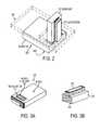
- FIG. 2is a perspective view of laser diode/submount assembly attached to a slider in accordance with the disclosure.
- FIG. 3Ais a perspective view of the solder and metallization area on the slider in accordance with the disclosure.
- FIG. 3Bis a perspective view of a laser diode/submount assembly in accordance with the disclosure.
- FIG. 4illustrates a thin film Au and platinum (Pt) barrier layer of a solder and metallization stack in accordance with the disclosure.
- connectionmeans any connection or coupling, either direct or indirect, between two or more elements, and can encompass the presence of one or more intermediate elements between two elements that are “connected” or “coupled” together.
- the coupling or connection between the elementscan be physical, logical, or a combination thereof.
- two elementscan be considered to be “connected” or “coupled” together by the use of one or more wires, cables, printed electrical connections, or any other suitable means.
- any reference to an element herein using a designation such as “first,” “second,” and so forthdoes not generally limit the quantity or order of those elements. Rather, these designations are used herein as a convenient method of distinguishing between two or more elements or instances of an element. Thus, a reference to first and second elements does not mean that only two elements can be employed, or that the first element must precede the second element.
- the thin filmincludes a substrate, a metallization layer on the substrate, and a cap layer on the metallization layer, wherein the cap layer includes a platinum (Pt) cap layer on the metallization layer, and an Au cap layer deposited on the Pt cap layer.
- Ptplatinum
- the thin filmincludes a Sn layer, a Pt layer on the Sn layer, and an Au layer on the Pt layer.
- the methodincludes disposing a Pt layer on a Sn layer and disposing a Au layer the Pt layer.
- aspects of a method of bonding a laser diode submount assembly to slider for a hard disk driveinclude disposing a first metallization layer on the slider, disposing a cap layer on the first metallization layer, wherein the cap layer includes a cap Pt layer on the first metallization layer, and a cap Au layer deposited on the cap Pt layer, disposing a second metallization layer on the laser diode submount assembly, and forming a solder bond between the cap layer on the slider and the second metallization layer on the laser diode submount assembly.
- the hard disk driveincludes magnetic disk, a head assembly comprising a slider, a first metallization layer on the slider, a laser diode submount assembly arranged with the slider, a cap layer on the first metallization layer, wherein the cap layer includes a cap Pt layer on the first metallization layer, a cap Au layer deposited on the cap Pt layer, and a second metallization layer on the laser diode submount assembly, wherein the cap layer on the slider is soldered to the second metallization layer on the laser diode submount assembly.
- FIG. 1is an exploded perspective view of an exemplary hard disk drive.
- the disk driveincludes a head disk assembly (HDA) 101 and a printed circuit board assembly (PCBA) 14 .
- the HDA 101includes a base 116 and cover 118 that together house at least one annular magnetic disk 120 .
- Each disk 120contains a plurality of magnetic tracks for storing data. The tracks are disposed upon opposing first and second disk surfaces of the disk 120 that extend between an inner disk edge 122 (corresponding to the inner diameter) and an outer disk edge 124 (corresponding to the outer diameter) of the disk 120 .
- the head disk assembly 110further includes a spindle motor 126 for rotating the disk 120 about a disk axis of rotation 128 .
- the spindle motor 126includes a spindle motor hub that is rotatably attached to the base 116 of the HDA 110 .
- Disks 120may be stacked and separated with one or more annular disk spacers 112 that are disposed about the hub, all held fixed to the hub by disk clamp 111 .
- the HDA 101further includes a head stack assembly (HSA) 30 rotatably attached to the base 116 of HDA 101 .
- the HSA 130includes an actuator comprising an actuator body 132 and one or more actuator arms 36 extending from the actuator body 132 .
- the actuator body 132includes a bore 144 and a pivot bearing cartridge engaged within the bore for facilitating the HSA 130 to rotate relative to HDA 101 about actuator pivot axis 146 .
- One or two head gimbal assemblies (HGA) 138are attached to a distal end of each actuator arm 136 .
- Each HGAincludes a head (e.g. head 140 ) for reading and writing data from and to the disk 120 , and a load beam 142 to compliantly preload the head against the disk 120 .
- the HSA 130further includes a coil support 148 that extends from one side of the HSA 130 that is opposite head 140 .
- the coil support 148is configured to support a coil 150 through which a changing electrical current is passed.
- the coil 150interacts with one or more magnets 154 that are attached to base 116 via a yoke structure 156 , 158 to form a voice coil motor for controllably rotating the HSA 130 .
- HDA 101includes a latch 152 rotatably mounted on base 116 to prevent undesired rotations of HSA 130 .
- the PCBA 114includes a servo control system for generating servo control signals to control the current through the coil 150 and thereby position the HSA 130 relative to tracks disposed upon surfaces of disk 120 .
- the PCBA 114also includes channel electronics to receive and provide electrical signals to the heads 140 of the HGAs 138 of the HSA 130 , e.g. for reading and writing data to the disks 10 .
- the HSA 130is electrically connected to PCBA 114 via a flexible printed circuit (FPC) 160 , which includes a flex cable 162 and a flex cable support bracket 164 .
- the flex cable 162supplies current to the coil 150 and carries signals between the HSA 130 and the PCBA 114 .
- the head 140is included in a slider (described in FIG. 2 ) that carries a magnetic transducer on its trailing end (not visible given the scale of FIG. 1 ).
- the magnetic transducermay include an inductive write element and a magnetoresistive read element.
- the transduceris separated from the magnetic disk by a very thin hydrodynamic air bearing.
- the hydrodynamic air bearingis formed between an air bearing surface of the slider of head 140 , and a surface of the magnetic disk 120 .
- the thickness of the air bearing at the location of the transduceris commonly referred to as “flying height.”
- the load beam 142(shown in dotted lines) supports a slider 201 (where the air bearing surface ABS is indicated on the bottom surface, not visible in this view).
- the slider 201may be further enhanced to include a laser diode LD 210 on a submount SM 220 to enable HAMR, which together may be referred to as an integrated HAMR head/laser assembly 200 .
- the integrated HAMR head/laser assembly 200includes two solder bonded interfaces a first to solder bond the LD 210 to the SM 220 with eutectic Au80Sn20 solder having a relatively high melting temperature ( ⁇ 300 C) and a second solder bond of the LD/SM assembly 220 to the slider with a lower melting temperature ( ⁇ 200 C) Sn-rich/Au solder.
- a Pt/Au capmay be used.
- the thin Pt layer in the thin film solderworks as barrier to prevent Au alloying with Sn during deposition and to better protect the surface of the Sn layer from environmental contamination, besides oxidation, including chemistry from photolithographic process.
- a structureis disclosed having metallization and solder stack pad deposited on a slider 300 in two steps that may be effected by E-beam evaporations and photolithographic resist lift-off process.
- the metallization layer 310 on the slider 300includes a Ti adhesion layer, a Pt low diffusive material barrier and an Au wetting layer.
- the solder layerincludes Sn and a cap layer to prevent Sn solder from oxidation/corrosion.
- the LD/SM assembly 210 / 220includes another bonding pad 330 on an end of the submount 220 that is soldered to the slider 300 , which may contain a metallization pad only for bonding the LD/SM assembly 210 / 220 to the slider 300 , as shown in FIG. 3B , and as shown assembled in the completed configuration in FIG. 2 .
- the soldermelts, and Au (e.g., from Under Bump Metallization (UBM), or Under Solder Metallization (USM)) dissolves into the Au/Sn solder of the adjacent part.
- UBMUnder Bump Metallization
- USMUnder Solder Metallization
- the composition of the metallizations and solder selected for this soldering processis chosen to have a lower melting point than that of the solder that joins the LD 210 to the submount 220 , insuring that the LD 210 will not detach from the submount 220 during this step.
- Intermetallic compounds (IMCs) formed between Sn and Aumay cause the solder to freeze by depletion of Sn or enriching the Au concentration, which causes the melting point to rise.
- At least two routesare available in the solder process, which may be used in combination. After the parts are aligned and brought in contact at ambient temperature, the parts may be heated. The rise in temperature results in melting of the solder. At this point, one or both of two processes may occur.
- the temperaturemay then be ramped down to cool and solidify the solder joint. Concurrently, as interdiffusion of Au and Sn proceeds, the melting point of the changing eutectic may rise, causing the solder to freeze, i.e., solidify.
- a combination of controlling the rate of cooling and the rate of interdiffusionmay be used to achieve the solder bond. If Sn-rich solder becomes oxidized or corroded during environmental exposure it will may become very difficult to achieve a reliable ultimate contact and precision alignment of the bonded parts. It may then require increasing bonding force to break surface oxides layer which may compromise these parts, including precision alignment. Also surface oxidation/corrosion may result in voids forming in the solder joint, resulting in lower bond strength, adversely affecting solder joint reliability.
- FIG. 4illustrates an exemplary structure having a Sn solder stack that may be include a thin Pt/Au cap.
- the stack in FIG. 4disposed on a substrate 400 , may include a Ti layer 410 , a Pt layer 420 , a Au layer 430 , referred to as the metallization layer, a Sn solder layer 440 , and a cap layer comprised of a Pt cap layer 450 and a Au cap layer 460 , referred to as the Sn-rich Au solder of FIG. 3A on the slider 300 .
- the Pt cap layer 450( ⁇ 5-15 nm) serves as a penetration barrier between the Au cap layer 460 and the Sn solder layer 440 .
- IMCs when the Pt cap layer 450 is not used in the Pt/Au capmay leave significant portions of the surface to consist of exposed Sn due to intermetallic migration of Au and Sn, which is prone to oxidation. This may result in lower shear flow bond strength of the HAMR integrated slider assembly (ISA) 200 , indicating a loss of bonding integrity, which may adversely affect bond strength, thermal and electrical conductivity through formation of solder voids. Additionally, with a thin layer of the Au cap layer 460 (e.g., ⁇ 25-100 nm) the shift in the eutectic melting point to a higher temperature may be limited.
Landscapes
- Engineering & Computer Science (AREA)
- Manufacturing & Machinery (AREA)
- Physics & Mathematics (AREA)
- Electromagnetism (AREA)
- Recording Or Reproducing By Magnetic Means (AREA)
- Magnetic Heads (AREA)
Abstract
Description
Claims (15)
Priority Applications (1)
| Application Number | Priority Date | Filing Date | Title |
|---|---|---|---|
| US14/051,397US9070387B1 (en) | 2013-08-23 | 2013-10-10 | Integrated heat-assisted magnetic recording head/laser assembly |
Applications Claiming Priority (2)
| Application Number | Priority Date | Filing Date | Title |
|---|---|---|---|
| US201361869155P | 2013-08-23 | 2013-08-23 | |
| US14/051,397US9070387B1 (en) | 2013-08-23 | 2013-10-10 | Integrated heat-assisted magnetic recording head/laser assembly |
Publications (1)
| Publication Number | Publication Date |
|---|---|
| US9070387B1true US9070387B1 (en) | 2015-06-30 |
Family
ID=53441823
Family Applications (1)
| Application Number | Title | Priority Date | Filing Date |
|---|---|---|---|
| US14/051,397ActiveUS9070387B1 (en) | 2013-08-23 | 2013-10-10 | Integrated heat-assisted magnetic recording head/laser assembly |
Country Status (1)
| Country | Link |
|---|---|
| US (1) | US9070387B1 (en) |
Cited By (3)
| Publication number | Priority date | Publication date | Assignee | Title |
|---|---|---|---|---|
| US9202478B1 (en) | 2015-02-10 | 2015-12-01 | Western Digital (Fremont), Llc | Method and structure for soldering a laser submount to a mounting face of a slider |
| US9786308B1 (en)* | 2016-06-07 | 2017-10-10 | Seagate Technology Llc | Interconnect interposer attachable to a trailing edge of a slider |
| US11508402B1 (en)* | 2021-09-16 | 2022-11-22 | Western Digital Technologies, Inc. | Slider assemblies having recesses with solder structures for magnetic recording devices, and related methods of forming slider assemblies |
Citations (146)
| Publication number | Priority date | Publication date | Assignee | Title |
|---|---|---|---|---|
| US3663184A (en) | 1970-01-23 | 1972-05-16 | Fairchild Camera Instr Co | Solder bump metallization system using a titanium-nickel barrier layer |
| US4817854A (en) | 1985-03-11 | 1989-04-04 | The United States Of America As Represented By The Secretary Of The Air Force | LED soldering method utilizing a PT migration barrier |
| US4836435A (en) | 1986-05-12 | 1989-06-06 | International Business Machines Corporation | Component self alignment |
| US5197654A (en) | 1991-11-15 | 1993-03-30 | Avishay Katz | Bonding method using solder composed of multiple alternating gold and tin layers |
| US5208186A (en) | 1989-02-09 | 1993-05-04 | National Semiconductor Corporation | Process for reflow bonding of bumps in IC devices |
| JPH05190973A (en) | 1992-01-14 | 1993-07-30 | Toshiba Corp | Submount for semiconductor laser |
| US5559817A (en) | 1994-11-23 | 1996-09-24 | Lucent Technologies Inc. | Complaint layer metallization |
| US5719070A (en) | 1992-05-11 | 1998-02-17 | International Business Machines Corporaton | Metallization composite having nickel intermediate/interface |
| US5990560A (en) | 1997-10-22 | 1999-11-23 | Lucent Technologies Inc. | Method and compositions for achieving a kinetically controlled solder bond |
| US6075673A (en) | 1997-05-05 | 2000-06-13 | Read-Rite Corporation | Composite slider design |
| US6097575A (en) | 1998-07-14 | 2000-08-01 | Read-Rite Corporation | Composite slider with housing and interlocked body |
| US6125014A (en) | 1998-06-26 | 2000-09-26 | Read-Rite Corporation | Via-less connection using interconnect traces between bond pads and a transducer coil of a magnetic head slider |
| US6125015A (en) | 1998-12-04 | 2000-09-26 | Read-Rite Corporation | Head gimbal assembly with low stiffness flex circuit and ESD Protection |
| US6130863A (en) | 1997-11-06 | 2000-10-10 | Read-Rite Corporation | Slider and electro-magnetic coil assembly |
| US6137656A (en) | 1998-10-26 | 2000-10-24 | Read-Rite Corporation | Air bearing slider |
| US6144528A (en) | 1998-10-26 | 2000-11-07 | Read-Rite Corporation | Air bearing slider with reduced stiction |
| US6147838A (en) | 1997-02-10 | 2000-11-14 | Read-Rite Corporation | Air bearing slider with shaped taper |
| US6151196A (en) | 1999-02-16 | 2000-11-21 | Read-Rite Corporation | Magnetic head suspension assembly including an intermediate flexible member that supports an air bearing slider with a magnetic transducer for testing |
| US6181522B1 (en) | 1998-12-12 | 2001-01-30 | Read-Write Corporation | Read/write head with a gimbal ball assembly |
| US6181673B1 (en) | 1996-07-30 | 2001-01-30 | Read-Rite Corporation | Slider design |
| US6229672B1 (en) | 1998-10-19 | 2001-05-08 | Read-Rite Corporation | High gram load air bearing geometry for a tripad slider |
| US6236543B1 (en) | 1999-01-29 | 2001-05-22 | Read-Rite Corporation | Durable landing pads for an air-bearing slider |
| US6246547B1 (en) | 1999-02-16 | 2001-06-12 | Read-Rite Corporation | Low profile flexure and slider-flexure assembly |
| US6249404B1 (en) | 1999-02-04 | 2001-06-19 | Read-Rite Corporation | Head gimbal assembly with a flexible printed circuit having a serpentine substrate |
| US6250541B1 (en) | 1997-06-23 | 2001-06-26 | Visteon Global Technologies, Inc. | Method of forming interconnections on electronic modules |
| US6330131B1 (en) | 1993-09-17 | 2001-12-11 | Read-Rite Corporation | Reduced stiction air bearing slider |
| US6349017B1 (en) | 1997-02-21 | 2002-02-19 | Read-Rite Corporation | Magnetic head suspension assembly using bonding pads of a slider to an attachment surface of a flexure |
| US6373660B1 (en) | 2000-03-14 | 2002-04-16 | Read-Rite Corporation | Method and system for providing a permanent shunt for a head gimbal assembly |
| US6391770B2 (en) | 1997-04-24 | 2002-05-21 | Mitsubishi Denki Kabushiki Kaisha | Method of manufacturing semiconductor device |
| US6522504B1 (en) | 2001-01-31 | 2003-02-18 | Western Digital Technologies, Inc. | Head stack assembly and disk drive using a reversed direction head gimbal assembly |
| US6538850B1 (en) | 1999-10-06 | 2003-03-25 | Read-Rite Corporation | Low profile head gimbal assembly with shock limiting and load/unload capability and method of manufacture thereof |
| US6548317B2 (en) | 1998-05-08 | 2003-04-15 | Sony Corporation | Photoelectric conversion element and method for manufacturing the same |
| US6548831B1 (en) | 1999-02-12 | 2003-04-15 | International Business Machines Corporation | Liquid crystal display panel having a gate line with at least one opening |
| US6583019B2 (en) | 2001-11-19 | 2003-06-24 | Gennum Corporation | Perimeter anchored thick film pad |
| US6583953B1 (en) | 1999-07-12 | 2003-06-24 | Mark Lauer | Silicon carbide overcoats for information storage systems and method of making |
| US6646832B2 (en) | 2001-01-29 | 2003-11-11 | Manuel Anaya-Dufresne | Slider for load/unload operation with high stiffness and low unload force |
| US6661612B1 (en) | 2001-10-21 | 2003-12-09 | Western Digital Technologies, Inc. | Air bearing slider including side rail shallow recessed surfaces extending along trailing portions of leading side air bearing surfaces |
| US6665146B2 (en) | 1999-12-28 | 2003-12-16 | Western Digital (Fremont) | Airflow assisted ramp loading and unloading of sliders in hard disk drives |
| US6690545B1 (en) | 2001-09-28 | 2004-02-10 | Western Digital Technologies, Inc. | Air bearing slider including a depressed region extending from a main support structure between a pressurized pad support base and a contact pad support base |
| US20040029304A1 (en) | 2002-03-27 | 2004-02-12 | Intel Corporation | Packaging of multiple active optical devices |
| US6704173B1 (en) | 2000-08-16 | 2004-03-09 | Western Digital (Fremont), Inc. | Method and system for providing ESD protection using diodes and a grounding strip in a head gimbal assembly |
| US6721142B1 (en) | 2000-12-21 | 2004-04-13 | Western Digital (Fremont) Inc. | Non-corrosive GMR slider for proximity recording |
| US6740822B2 (en) | 2001-03-23 | 2004-05-25 | Kabushiki Kaisha Toshiba | Printed circuit board having footprints, circuit module having a printed circuit board, and method of manufacturing a printed circuit board |
| US6744599B1 (en) | 2002-04-30 | 2004-06-01 | Western Digital Technologies, Inc. | Air bearing slider with an angularly disposed channel formed between a side rail and a leading side air bearing surface |
| US6762123B2 (en) | 1999-11-22 | 2004-07-13 | Stmicroelectronics S.R.L. | Moisture corrosion inhibitor layer for Al-alloy metallization layers, particularly for electronic devices and corresponding manufacturing method |
| US6771468B1 (en) | 2001-10-22 | 2004-08-03 | Western Digital Corporation | Slider with high pitch-stiffness air bearing design |
| US6796018B1 (en) | 2001-12-21 | 2004-09-28 | Western Digital (Fremont), Inc. | Method of forming a slider/suspension assembly |
| US6801402B1 (en) | 2002-10-31 | 2004-10-05 | Western Digital Technologies, Inc. | ESD-protected head gimbal assembly for use in a disk drive |
| US6873496B1 (en) | 2000-01-03 | 2005-03-29 | Western Digital Fremont, Inc. | Side rail slider having improved fly height control |
| US6912103B1 (en) | 2002-07-31 | 2005-06-28 | Western Digital Technologies, Inc. | Method of operating a disk drive with a slider at loading and unloading fly heights greater than an operational fly height |
| US6930389B2 (en) | 2003-06-30 | 2005-08-16 | Advanced Semiconductor Engineering, Inc. | Under bump metallization structure of a semiconductor wafer |
| US6937439B1 (en) | 2001-11-30 | 2005-08-30 | Western Digital Technologies, Inc. | Slider having a textured air bearing surface, head stack assembly and disk drive using same |
| US20050227413A1 (en) | 2004-03-01 | 2005-10-13 | Joachim John | Method for depositing a solder material on a substrate |
| US6956718B1 (en) | 2002-08-19 | 2005-10-18 | Western Digital (Fremont), Inc. | Sandwich diamond-like carbon overcoat for use in slider designs of proximity recording heads |
| US6972930B1 (en) | 2003-02-28 | 2005-12-06 | Western Digital Technologies, Inc. | ESD-protected slider and head gimbal assembly |
| US7006330B1 (en) | 2003-03-10 | 2006-02-28 | Western Digital Technologies, Inc. | Head stack assembly including a ground conductive pad for grounding a slider to a gimbal |
| US7006331B1 (en) | 2003-09-30 | 2006-02-28 | Western Digital Technologies, Inc. | Head gimbal assembly including a trace suspension assembly backing layer with a conductive layer formed upon a gimbal having a lower oxidation rate |
| US7015583B2 (en) | 2002-04-30 | 2006-03-21 | Sumitomo Electric Industries, Ltd. | Submount and semiconductor device |
| US7019945B1 (en) | 2002-12-23 | 2006-03-28 | Western Digital Technologies, Inc. | Air bearing slider including pressurized side pads with forward and trailing shallow etched surfaces |
| US7027264B1 (en) | 2003-10-31 | 2006-04-11 | Western Digital Technologies, Inc. | Slider with a slider ground pad electrically connected to write head poles and read head shields |
| US7085104B1 (en) | 1999-10-06 | 2006-08-01 | Western Digital (Fremont), Inc. | Low profile head gimbal assembly with shock limiting and load/unload capability |
| US7099117B1 (en) | 2003-09-30 | 2006-08-29 | Western Digital Technologies, Inc. | Head stack assembly including a trace suspension assembly backing layer and a ground trace for grounding a slider |
| US7168608B2 (en) | 2002-12-24 | 2007-01-30 | Avago Technologies General Ip (Singapore) Pte. Ltd. | System and method for hermetic seal formation |
| US7196356B2 (en) | 2002-08-09 | 2007-03-27 | Sumitomo Electric Industries, Ltd. | Submount and semiconductor device |
| US7245014B2 (en) | 2003-05-20 | 2007-07-17 | Sharp Kabushiki Kaisha | Semiconductor light emitting apparatus and method for producing the same |
| US7276386B2 (en) | 1999-04-26 | 2007-10-02 | Fujitsu Limited | Semiconductor device and method of manufacturing the same |
| US20070228105A1 (en) | 2006-03-31 | 2007-10-04 | Yoshikazu Oshika | Solder layer and electronic device bonding substrate and submount using the same |
| US7289299B1 (en) | 2005-02-02 | 2007-10-30 | Western Digital (Fremont), Llc | Air bearing slider with three-projection trailing center pad |
| US7298049B2 (en) | 2002-03-06 | 2007-11-20 | Sumitomo Electric Industries, Ltd. | Submount for mounting semiconductor device |
| US20070273025A1 (en) | 2002-11-06 | 2007-11-29 | Koninklijke Philips Electronics N.V. | Device Comprising Circuit Elements Connected By Bonding Bump Structure |
| US7307816B1 (en) | 2001-12-21 | 2007-12-11 | Western Digital (Fremont), Llc | Flexure design and assembly process for attachment of slider using solder and laser reflow |
| US7315435B1 (en) | 2005-03-17 | 2008-01-01 | Western Digital Technologies, Inc. | Disk drives, head stack, head gimbal and suspension assemblies having positional conductive features |
| US7315436B1 (en) | 2004-06-25 | 2008-01-01 | Western Digital Technologies, Inc. | Suspension assembly with a shape memory actuator coupled to a gimbal |
| US7368666B2 (en) | 2005-02-22 | 2008-05-06 | Alps Electric Co., Ltd | Surface-mounting type electronic circuit unit without detachment of solder |
| US7372142B2 (en) | 2004-05-31 | 2008-05-13 | Stmicroelectronics, S.R.L. | Vertical conduction power electronic device package and corresponding assembling method |
| US7414814B1 (en) | 2005-04-28 | 2008-08-19 | Western Digital Technologies, Inc. | Disk drives, head stack, head gimbal and suspension assemblies having a compliant suspension tail design for solder reflow |
| US7436631B1 (en) | 2004-06-30 | 2008-10-14 | Western Digital (Fremont), Llc | Heated gimbal for magnetic head to disk clearance adjustment |
| US7463454B2 (en) | 2002-06-20 | 2008-12-09 | Stmicroelectronics S.R.L. | Micro-actuator for hard drive utilizing insulating portions to separate biasing regions from adjacent regions of the micro-actuator and simplified manufacture process therefore |
| US7462861B2 (en) | 2004-04-28 | 2008-12-09 | Cree, Inc. | LED bonding structures and methods of fabricating LED bonding structures |
| US7474508B1 (en) | 2005-03-09 | 2009-01-06 | Western Digital (Fremont), Inc. | Head gimbal assembly with air bearing slider crown having reduced temperature sensitivity |
| US7477486B1 (en) | 2005-12-07 | 2009-01-13 | Western Digital (Fremont), Llc | Air bearing slider with a side pad having a shallow recess depth |
| US20090091024A1 (en) | 2007-06-11 | 2009-04-09 | Texas Instruments Incorporated | Stable Gold Bump Solder Connections |
| US7595963B1 (en) | 2006-06-07 | 2009-09-29 | Western Digital Technologies, Inc. | Head gimbal assembly including a flexure with a first conductive trace disposed between a slider and a dielectric layer |
| US7601625B2 (en) | 2004-04-20 | 2009-10-13 | Denso Corporation | Method for manufacturing semiconductor device having solder layer |
| US7616405B2 (en) | 2006-11-15 | 2009-11-10 | Western Digital (Fremont), Llc | Slider with an air bearing surface having a inter-cavity dam with OD and ID dam surfaces of different heights |
| US7729089B1 (en) | 2006-10-13 | 2010-06-01 | Western Digital Technologies, Inc. | Head-gimbal assembly including a flexure tongue with stand-offs arranged to facilitate lateral light entry |
| US20100244239A1 (en) | 2009-03-24 | 2010-09-30 | Stats Chippac, Ltd. | Semiconductor Device and Method of Forming Enhanced UBM Structure for Improving Solder Joint Reliability |
| US7995310B1 (en) | 2006-11-09 | 2011-08-09 | Western Digital Technologies, Inc. | Head-gimbal assembly including a flexure tongue with adhesive receptacles disposed adjacent to stand-offs |
| US20110205860A1 (en) | 2010-02-22 | 2011-08-25 | Tdk Corporation | Heat-assisted magnetic recording head including plasmon generator |
| US8018685B2 (en) | 2008-10-16 | 2011-09-13 | Tdk Corporation | Head gimbal assembly for heat-assisted magnetic recording |
| US8081400B1 (en) | 2008-08-29 | 2011-12-20 | Western Digital (Fremont), Llc | Slider with an air-bearing surface including four pressure generating pockets for countering disruptive movement |
| US8089730B1 (en) | 2009-10-28 | 2012-01-03 | Western Digital (Fremont), Llc | Suspension assembly having a read head clamp |
| US8087973B1 (en) | 2008-08-19 | 2012-01-03 | Western Digital (Fremont), Llc | Slider with leading edge blend and conformal step features |
| US8164858B1 (en) | 2009-11-04 | 2012-04-24 | Western Digital (Fremont), Llc | Read head having conductive filler in insulated hole through substrate |
| US8199437B1 (en) | 2010-03-09 | 2012-06-12 | Western Digital (Fremont), Llc | Head with an air bearing surface having a particle fence separated from a leading pad by a continuous moat |
| US8208224B1 (en) | 2011-08-29 | 2012-06-26 | Western Digital Technologies, Inc. | Suspension assemblies for minimizing stress on slider solder joints |
| US20120163138A1 (en) | 2010-12-22 | 2012-06-28 | Seagate Technology Llc | Integrated Heat Assisted Magnetic Recording Head With Extended Cavity Vertical Cavity Surface Emitting Laser Diode |
| US8218268B1 (en) | 2009-05-27 | 2012-07-10 | Western Digital Technologies, Inc. | Head gimbal assembly having a load beam aperature over conductive heating pads that are offset from head bonding pads |
| US8240545B1 (en) | 2011-08-11 | 2012-08-14 | Western Digital (Fremont), Llc | Methods for minimizing component shift during soldering |
| US8254212B2 (en) | 2009-06-25 | 2012-08-28 | Seagate Technology Llc | Integrated heat assisted magnetic recording device |
| US8256272B1 (en) | 2009-12-23 | 2012-09-04 | Western Digital (Fremont), Llc | UV adhesive viscosity adjustment apparatus and method |
| US8295012B1 (en) | 2011-06-14 | 2012-10-23 | Western Digital Technologies, Inc. | Disk drive suspension assembly with rotary fine actuator at flexure tongue |
| US8295013B1 (en) | 2010-10-29 | 2012-10-23 | Western Digital Technologies, Inc. | Disk drive head stack assembly having a flexible printed circuit with heat transfer limiting features |
| US8295014B1 (en) | 2010-10-29 | 2012-10-23 | Western Digital Technologies, Inc. | Disk drive head gimbal assembly having a flexure tail with transverse flying leads |
| US8320084B1 (en) | 2010-10-29 | 2012-11-27 | Western Digital Technologies, Inc. | Disk drive head gimbal assembly having a flexure tail with features to facilitate bonding |
| US8325446B1 (en) | 2010-10-29 | 2012-12-04 | Western Digital Technologies, Inc. | Disk drive head gimbal assembly having a flexure tail with features to facilitate bonding |
| US8339748B2 (en) | 2010-06-29 | 2012-12-25 | Western Digital Technologies, Inc. | Suspension assembly having a microactuator bonded to a flexure |
| US8339747B1 (en) | 2011-03-11 | 2012-12-25 | Western Digital Technologies, Inc. | Removable actuator assemblies for testing head gimbal assemblies of a storage device |
| US8343363B1 (en) | 2010-03-10 | 2013-01-01 | Western Digital (Fremont), Llc | Method and system for fabricating a cavity in a substrate of a magnetic recording head |
| US8345519B1 (en) | 2010-12-22 | 2013-01-01 | Western Digital (Fremont), Llc | Method and system for providing a suspension head bond pad design |
| US20130016591A1 (en) | 2011-07-14 | 2013-01-17 | Tdk Corporation | Thermally-assisted magnetic recording medium and magnetic recording/reproducing device using the same |
| US8418353B1 (en) | 2009-12-23 | 2013-04-16 | Western Digital (Fremont), Llc | Method for providing a plurality of energy assisted magnetic recording EAMR heads |
| US8441896B2 (en) | 2010-06-25 | 2013-05-14 | Western Digital (Fremont), Llc | Energy assisted magnetic recording head having laser integrated mounted to slider |
| US8446694B1 (en) | 2011-06-14 | 2013-05-21 | Western Digital Technologies, Inc. | Disk drive head suspension assembly with embedded in-plane actuator at flexure tongue |
| US8456776B1 (en) | 2010-09-22 | 2013-06-04 | Western Digital Technologies, Inc. | Disk drive head gimbal assembly having a flexure bond pad shelf offset from a tongue |
| US8456643B2 (en) | 2010-05-24 | 2013-06-04 | Western Digital (Fremont), Llc | Method and system for mapping the shape of a head under operating conditions |
| US8462462B1 (en) | 2011-10-20 | 2013-06-11 | Western Digital (Fremont), Llc | Localized heating for flip chip bonding |
| US8477459B1 (en) | 2010-10-29 | 2013-07-02 | Western Digital Technologies, Inc. | Disk drive head gimbal assembly having a flexure tail with dual conductive layers and features to facilitate bonding |
| US8485579B2 (en) | 2011-03-17 | 2013-07-16 | Western Digital (Fremont), Llc | Vacuum pickup assemblies for picking up articles and minimizing contamination thereof |
| US8488279B1 (en) | 2011-11-22 | 2013-07-16 | Western Digital (Fremont), Llc | Disk drive suspension assembly with flexure having stacked interleaved traces |
| US8490211B1 (en) | 2012-06-28 | 2013-07-16 | Western Digital Technologies, Inc. | Methods for referencing related magnetic head microscopy scans to reduce processing requirements for high resolution imaging |
| US8488281B1 (en) | 2011-09-13 | 2013-07-16 | Western Digital (Fremont), Llc | Disk drive suspension assembly having a flexure bond pad shelf separate from a tongue |
| US8514522B1 (en) | 2011-01-25 | 2013-08-20 | Western Digital (Fremont), Llc | Systems for interconnecting magnetic heads of storage devices in a test assembly |
| US8533936B1 (en) | 2011-01-26 | 2013-09-17 | Western Digital (Fremont), Llc | Systems and methods for pre-heating adjacent bond pads for soldering |
| US20130244541A1 (en) | 2012-03-14 | 2013-09-19 | Western Digital Technologies, Inc. | Systems and methods for correcting slider parallelism error using compensation lapping |
| US8545164B2 (en) | 2010-12-06 | 2013-10-01 | Western Digital (Fremont), Llc | Systems and methods for repositioning row bars used for manufacturing magnetic heads |
| US8553365B1 (en) | 2012-02-21 | 2013-10-08 | Western Digital (Fremont), Llc | Apparatuses and methods for loading a head onto a disk medium |
| US20130293982A1 (en) | 2012-05-02 | 2013-11-07 | Western Digital Technologies, Inc. | Disk drive employing single polarity supply voltage to generate write current |
| US8587901B1 (en) | 2009-12-30 | 2013-11-19 | Western Digital (Fremont), Llc | Magnetic recording head slider comprising bond pad having a probe contact area and a solder contact area |
| US8593764B1 (en) | 2011-06-14 | 2013-11-26 | Western Digital Technologies, Inc. | Method for fine actuation of a head during operation of a disk drive |
| US8599653B1 (en) | 2012-09-11 | 2013-12-03 | Western Digital Technologies, Inc. | Systems and methods for reducing condensation along a slider air bearing surface in energy assisted magnetic recording |
| US8605389B1 (en) | 2006-06-09 | 2013-12-10 | Western Digital Technologies, Inc. | Head gimbal assembly including a conductive trace disposed upon a continuous dielectric layer segment without overlying a gimbal arm |
| US8611052B1 (en) | 2012-03-27 | 2013-12-17 | Western Digital Technologies, Inc. | Systems and methods for aligning components of a head stack assembly of a hard disk drive |
| US8623197B1 (en) | 2010-12-20 | 2014-01-07 | Western Digital (Fremont), Llc | Testing workpiece overcoat |
| US8624184B1 (en) | 2012-11-28 | 2014-01-07 | Western Digital Technologies, Inc. | Methods for spatially resolved alignment of independent spectroscopic data from scanning transmission electron microscopes |
| US8665567B2 (en) | 2010-06-30 | 2014-03-04 | Western Digital Technologies, Inc. | Suspension assembly having a microactuator grounded to a flexure |
| US8665677B1 (en) | 2011-12-19 | 2014-03-04 | Western Digital (Fremont), Llc | Disk drive magnetic read head with affixed and recessed laser device |
| US8665566B1 (en) | 2011-12-20 | 2014-03-04 | Western Digital Technologies, Inc. | Suspension tail design for a head gimbal assembly of a hard disk drive |
| US8693144B1 (en) | 2013-03-15 | 2014-04-08 | Western Digital Technologies, Inc. | Head gimbal assemblies and methods for measuring slider parameters |
| US8758083B1 (en) | 2010-09-13 | 2014-06-24 | Western Digital (Fremont), Llc | Method and system for adjusting lapping of a transducer using a disk windage |
| US8760812B1 (en) | 2011-12-20 | 2014-06-24 | Western Digital Technologies, Inc. | Disk drive head gimbal assembly having a jumper in a flexible printed circuit overlap region |
| US8770463B1 (en) | 2013-05-20 | 2014-07-08 | Western Digital Technologies, Inc. | Head gimbal assembly carrier with adjustable protective bar |
| US8773664B1 (en) | 2011-12-20 | 2014-07-08 | Western Digital (Fremont), Llc | Method and system for aligning substrates for direct laser coupling in an energy assisted magnetic recording head |
| US8792212B1 (en) | 2010-09-14 | 2014-07-29 | Western Digital (Fremont), Llc | Robust gimbal design for head gimbal assembly |
| US8792213B1 (en) | 2013-02-20 | 2014-07-29 | Western Digital Technologies, Inc. | Tethered gimbal on suspension for improved flyability |
| US8797691B1 (en) | 2013-05-21 | 2014-08-05 | Western Digital Technologies, Inc. | Disk drive head suspension with a single piezoelectric element adhered to rotary-actuated and non-actuated portions of a structural layer of a tongue of a laminated flexure |
- 2013
- 2013-10-10USUS14/051,397patent/US9070387B1/enactiveActive
Patent Citations (160)
| Publication number | Priority date | Publication date | Assignee | Title |
|---|---|---|---|---|
| US3663184A (en) | 1970-01-23 | 1972-05-16 | Fairchild Camera Instr Co | Solder bump metallization system using a titanium-nickel barrier layer |
| US4817854A (en) | 1985-03-11 | 1989-04-04 | The United States Of America As Represented By The Secretary Of The Air Force | LED soldering method utilizing a PT migration barrier |
| US4836435A (en) | 1986-05-12 | 1989-06-06 | International Business Machines Corporation | Component self alignment |
| US5208186A (en) | 1989-02-09 | 1993-05-04 | National Semiconductor Corporation | Process for reflow bonding of bumps in IC devices |
| US5197654A (en) | 1991-11-15 | 1993-03-30 | Avishay Katz | Bonding method using solder composed of multiple alternating gold and tin layers |
| JPH05190973A (en) | 1992-01-14 | 1993-07-30 | Toshiba Corp | Submount for semiconductor laser |
| US5719070A (en) | 1992-05-11 | 1998-02-17 | International Business Machines Corporaton | Metallization composite having nickel intermediate/interface |
| US6330131B1 (en) | 1993-09-17 | 2001-12-11 | Read-Rite Corporation | Reduced stiction air bearing slider |
| US5559817A (en) | 1994-11-23 | 1996-09-24 | Lucent Technologies Inc. | Complaint layer metallization |
| US6181673B1 (en) | 1996-07-30 | 2001-01-30 | Read-Rite Corporation | Slider design |
| US6339518B1 (en) | 1997-02-10 | 2002-01-15 | Read-Rite Corporation | Air bearing slider with shaped taper |
| US6147838A (en) | 1997-02-10 | 2000-11-14 | Read-Rite Corporation | Air bearing slider with shaped taper |
| US6178064B1 (en) | 1997-02-10 | 2001-01-23 | Read-Rite Corporation | Air bearing slider with shaped taper |
| US6349017B1 (en) | 1997-02-21 | 2002-02-19 | Read-Rite Corporation | Magnetic head suspension assembly using bonding pads of a slider to an attachment surface of a flexure |
| US6391770B2 (en) | 1997-04-24 | 2002-05-21 | Mitsubishi Denki Kabushiki Kaisha | Method of manufacturing semiconductor device |
| US6075673A (en) | 1997-05-05 | 2000-06-13 | Read-Rite Corporation | Composite slider design |
| US6250541B1 (en) | 1997-06-23 | 2001-06-26 | Visteon Global Technologies, Inc. | Method of forming interconnections on electronic modules |
| US5990560A (en) | 1997-10-22 | 1999-11-23 | Lucent Technologies Inc. | Method and compositions for achieving a kinetically controlled solder bond |
| US6130863A (en) | 1997-11-06 | 2000-10-10 | Read-Rite Corporation | Slider and electro-magnetic coil assembly |
| US6548317B2 (en) | 1998-05-08 | 2003-04-15 | Sony Corporation | Photoelectric conversion element and method for manufacturing the same |
| US6125014A (en) | 1998-06-26 | 2000-09-26 | Read-Rite Corporation | Via-less connection using interconnect traces between bond pads and a transducer coil of a magnetic head slider |
| US6097575A (en) | 1998-07-14 | 2000-08-01 | Read-Rite Corporation | Composite slider with housing and interlocked body |
| US6229672B1 (en) | 1998-10-19 | 2001-05-08 | Read-Rite Corporation | High gram load air bearing geometry for a tripad slider |
| US6144528A (en) | 1998-10-26 | 2000-11-07 | Read-Rite Corporation | Air bearing slider with reduced stiction |
| US6137656A (en) | 1998-10-26 | 2000-10-24 | Read-Rite Corporation | Air bearing slider |
| US6125015A (en) | 1998-12-04 | 2000-09-26 | Read-Rite Corporation | Head gimbal assembly with low stiffness flex circuit and ESD Protection |
| US6378195B1 (en) | 1998-12-12 | 2002-04-30 | Read-Rite Corporation | Read/write head with a gimbal ball assembly |
| US6181522B1 (en) | 1998-12-12 | 2001-01-30 | Read-Write Corporation | Read/write head with a gimbal ball assembly |
| US6236543B1 (en) | 1999-01-29 | 2001-05-22 | Read-Rite Corporation | Durable landing pads for an air-bearing slider |
| US6249404B1 (en) | 1999-02-04 | 2001-06-19 | Read-Rite Corporation | Head gimbal assembly with a flexible printed circuit having a serpentine substrate |
| US6548831B1 (en) | 1999-02-12 | 2003-04-15 | International Business Machines Corporation | Liquid crystal display panel having a gate line with at least one opening |
| US6246547B1 (en) | 1999-02-16 | 2001-06-12 | Read-Rite Corporation | Low profile flexure and slider-flexure assembly |
| US6151196A (en) | 1999-02-16 | 2000-11-21 | Read-Rite Corporation | Magnetic head suspension assembly including an intermediate flexible member that supports an air bearing slider with a magnetic transducer for testing |
| US6708389B1 (en) | 1999-02-16 | 2004-03-23 | Western Digital (Fremont), Inc. | Method of forming a magnetic head suspension assembly |
| US7276386B2 (en) | 1999-04-26 | 2007-10-02 | Fujitsu Limited | Semiconductor device and method of manufacturing the same |
| US6583953B1 (en) | 1999-07-12 | 2003-06-24 | Mark Lauer | Silicon carbide overcoats for information storage systems and method of making |
| US7085104B1 (en) | 1999-10-06 | 2006-08-01 | Western Digital (Fremont), Inc. | Low profile head gimbal assembly with shock limiting and load/unload capability |
| US7010847B1 (en) | 1999-10-06 | 2006-03-14 | Western Digital (Fremont), Inc. | Method of manufacturing a head gimbal assembly with substantially orthogonal tab, side beam and base |
| US6538850B1 (en) | 1999-10-06 | 2003-03-25 | Read-Rite Corporation | Low profile head gimbal assembly with shock limiting and load/unload capability and method of manufacture thereof |
| US6762123B2 (en) | 1999-11-22 | 2004-07-13 | Stmicroelectronics S.R.L. | Moisture corrosion inhibitor layer for Al-alloy metallization layers, particularly for electronic devices and corresponding manufacturing method |
| US6665146B2 (en) | 1999-12-28 | 2003-12-16 | Western Digital (Fremont) | Airflow assisted ramp loading and unloading of sliders in hard disk drives |
| US6717773B2 (en) | 1999-12-28 | 2004-04-06 | Western Digital (Fremont), Inc. | Airflow assisted ramp loading and unloading of sliders in hard disk drives |
| US6856489B2 (en) | 1999-12-28 | 2005-02-15 | Western Digital (Fremont), Inc. | Airflow assisted ramp loading and unloading of sliders in hard disk drives |
| US6873496B1 (en) | 2000-01-03 | 2005-03-29 | Western Digital Fremont, Inc. | Side rail slider having improved fly height control |
| US6373660B1 (en) | 2000-03-14 | 2002-04-16 | Read-Rite Corporation | Method and system for providing a permanent shunt for a head gimbal assembly |
| US6704173B1 (en) | 2000-08-16 | 2004-03-09 | Western Digital (Fremont), Inc. | Method and system for providing ESD protection using diodes and a grounding strip in a head gimbal assembly |
| US7174622B2 (en) | 2000-12-21 | 2007-02-13 | Western Digital (Fremont), Inc. | Process of making a non-corrosive GMR slider for proximity recording |
| US6721142B1 (en) | 2000-12-21 | 2004-04-13 | Western Digital (Fremont) Inc. | Non-corrosive GMR slider for proximity recording |
| US6646832B2 (en) | 2001-01-29 | 2003-11-11 | Manuel Anaya-Dufresne | Slider for load/unload operation with high stiffness and low unload force |
| US6522504B1 (en) | 2001-01-31 | 2003-02-18 | Western Digital Technologies, Inc. | Head stack assembly and disk drive using a reversed direction head gimbal assembly |
| US6740822B2 (en) | 2001-03-23 | 2004-05-25 | Kabushiki Kaisha Toshiba | Printed circuit board having footprints, circuit module having a printed circuit board, and method of manufacturing a printed circuit board |
| US6690545B1 (en) | 2001-09-28 | 2004-02-10 | Western Digital Technologies, Inc. | Air bearing slider including a depressed region extending from a main support structure between a pressurized pad support base and a contact pad support base |
| US6661612B1 (en) | 2001-10-21 | 2003-12-09 | Western Digital Technologies, Inc. | Air bearing slider including side rail shallow recessed surfaces extending along trailing portions of leading side air bearing surfaces |
| US6771468B1 (en) | 2001-10-22 | 2004-08-03 | Western Digital Corporation | Slider with high pitch-stiffness air bearing design |
| US6583019B2 (en) | 2001-11-19 | 2003-06-24 | Gennum Corporation | Perimeter anchored thick film pad |
| US6937439B1 (en) | 2001-11-30 | 2005-08-30 | Western Digital Technologies, Inc. | Slider having a textured air bearing surface, head stack assembly and disk drive using same |
| US7307816B1 (en) | 2001-12-21 | 2007-12-11 | Western Digital (Fremont), Llc | Flexure design and assembly process for attachment of slider using solder and laser reflow |
| US6796018B1 (en) | 2001-12-21 | 2004-09-28 | Western Digital (Fremont), Inc. | Method of forming a slider/suspension assembly |
| US7593190B1 (en) | 2001-12-21 | 2009-09-22 | Western Digital (Fremont), Llc | Flexure design and assembly process for attachment of slider using solder and laser reflow |
| US7298049B2 (en) | 2002-03-06 | 2007-11-20 | Sumitomo Electric Industries, Ltd. | Submount for mounting semiconductor device |
| US20040029304A1 (en) | 2002-03-27 | 2004-02-12 | Intel Corporation | Packaging of multiple active optical devices |
| US7015583B2 (en) | 2002-04-30 | 2006-03-21 | Sumitomo Electric Industries, Ltd. | Submount and semiconductor device |
| US6744599B1 (en) | 2002-04-30 | 2004-06-01 | Western Digital Technologies, Inc. | Air bearing slider with an angularly disposed channel formed between a side rail and a leading side air bearing surface |
| US7463454B2 (en) | 2002-06-20 | 2008-12-09 | Stmicroelectronics S.R.L. | Micro-actuator for hard drive utilizing insulating portions to separate biasing regions from adjacent regions of the micro-actuator and simplified manufacture process therefore |
| US6912103B1 (en) | 2002-07-31 | 2005-06-28 | Western Digital Technologies, Inc. | Method of operating a disk drive with a slider at loading and unloading fly heights greater than an operational fly height |
| US7196356B2 (en) | 2002-08-09 | 2007-03-27 | Sumitomo Electric Industries, Ltd. | Submount and semiconductor device |
| US6956718B1 (en) | 2002-08-19 | 2005-10-18 | Western Digital (Fremont), Inc. | Sandwich diamond-like carbon overcoat for use in slider designs of proximity recording heads |
| US6801402B1 (en) | 2002-10-31 | 2004-10-05 | Western Digital Technologies, Inc. | ESD-protected head gimbal assembly for use in a disk drive |
| US20070273025A1 (en) | 2002-11-06 | 2007-11-29 | Koninklijke Philips Electronics N.V. | Device Comprising Circuit Elements Connected By Bonding Bump Structure |
| US7019945B1 (en) | 2002-12-23 | 2006-03-28 | Western Digital Technologies, Inc. | Air bearing slider including pressurized side pads with forward and trailing shallow etched surfaces |
| US7168608B2 (en) | 2002-12-24 | 2007-01-30 | Avago Technologies General Ip (Singapore) Pte. Ltd. | System and method for hermetic seal formation |
| US6972930B1 (en) | 2003-02-28 | 2005-12-06 | Western Digital Technologies, Inc. | ESD-protected slider and head gimbal assembly |
| US7006330B1 (en) | 2003-03-10 | 2006-02-28 | Western Digital Technologies, Inc. | Head stack assembly including a ground conductive pad for grounding a slider to a gimbal |
| US7245014B2 (en) | 2003-05-20 | 2007-07-17 | Sharp Kabushiki Kaisha | Semiconductor light emitting apparatus and method for producing the same |
| US6930389B2 (en) | 2003-06-30 | 2005-08-16 | Advanced Semiconductor Engineering, Inc. | Under bump metallization structure of a semiconductor wafer |
| US7006331B1 (en) | 2003-09-30 | 2006-02-28 | Western Digital Technologies, Inc. | Head gimbal assembly including a trace suspension assembly backing layer with a conductive layer formed upon a gimbal having a lower oxidation rate |
| US7099117B1 (en) | 2003-09-30 | 2006-08-29 | Western Digital Technologies, Inc. | Head stack assembly including a trace suspension assembly backing layer and a ground trace for grounding a slider |
| US7027264B1 (en) | 2003-10-31 | 2006-04-11 | Western Digital Technologies, Inc. | Slider with a slider ground pad electrically connected to write head poles and read head shields |
| US20050227413A1 (en) | 2004-03-01 | 2005-10-13 | Joachim John | Method for depositing a solder material on a substrate |
| US7601625B2 (en) | 2004-04-20 | 2009-10-13 | Denso Corporation | Method for manufacturing semiconductor device having solder layer |
| US7462861B2 (en) | 2004-04-28 | 2008-12-09 | Cree, Inc. | LED bonding structures and methods of fabricating LED bonding structures |
| US7372142B2 (en) | 2004-05-31 | 2008-05-13 | Stmicroelectronics, S.R.L. | Vertical conduction power electronic device package and corresponding assembling method |
| US7315436B1 (en) | 2004-06-25 | 2008-01-01 | Western Digital Technologies, Inc. | Suspension assembly with a shape memory actuator coupled to a gimbal |
| US7436631B1 (en) | 2004-06-30 | 2008-10-14 | Western Digital (Fremont), Llc | Heated gimbal for magnetic head to disk clearance adjustment |
| US7289299B1 (en) | 2005-02-02 | 2007-10-30 | Western Digital (Fremont), Llc | Air bearing slider with three-projection trailing center pad |
| US7368666B2 (en) | 2005-02-22 | 2008-05-06 | Alps Electric Co., Ltd | Surface-mounting type electronic circuit unit without detachment of solder |
| US7474508B1 (en) | 2005-03-09 | 2009-01-06 | Western Digital (Fremont), Inc. | Head gimbal assembly with air bearing slider crown having reduced temperature sensitivity |
| US7315435B1 (en) | 2005-03-17 | 2008-01-01 | Western Digital Technologies, Inc. | Disk drives, head stack, head gimbal and suspension assemblies having positional conductive features |
| US7414814B1 (en) | 2005-04-28 | 2008-08-19 | Western Digital Technologies, Inc. | Disk drives, head stack, head gimbal and suspension assemblies having a compliant suspension tail design for solder reflow |
| US7477486B1 (en) | 2005-12-07 | 2009-01-13 | Western Digital (Fremont), Llc | Air bearing slider with a side pad having a shallow recess depth |
| US20070228105A1 (en) | 2006-03-31 | 2007-10-04 | Yoshikazu Oshika | Solder layer and electronic device bonding substrate and submount using the same |
| US7595963B1 (en) | 2006-06-07 | 2009-09-29 | Western Digital Technologies, Inc. | Head gimbal assembly including a flexure with a first conductive trace disposed between a slider and a dielectric layer |
| US8605389B1 (en) | 2006-06-09 | 2013-12-10 | Western Digital Technologies, Inc. | Head gimbal assembly including a conductive trace disposed upon a continuous dielectric layer segment without overlying a gimbal arm |
| US7729089B1 (en) | 2006-10-13 | 2010-06-01 | Western Digital Technologies, Inc. | Head-gimbal assembly including a flexure tongue with stand-offs arranged to facilitate lateral light entry |
| US7995310B1 (en) | 2006-11-09 | 2011-08-09 | Western Digital Technologies, Inc. | Head-gimbal assembly including a flexure tongue with adhesive receptacles disposed adjacent to stand-offs |
| US7616405B2 (en) | 2006-11-15 | 2009-11-10 | Western Digital (Fremont), Llc | Slider with an air bearing surface having a inter-cavity dam with OD and ID dam surfaces of different heights |
| US20090091024A1 (en) | 2007-06-11 | 2009-04-09 | Texas Instruments Incorporated | Stable Gold Bump Solder Connections |
| US8339742B1 (en) | 2008-08-19 | 2012-12-25 | Western Digital (Fremont), Llc | Slider with leading edge blend and conformal step features |
| US8087973B1 (en) | 2008-08-19 | 2012-01-03 | Western Digital (Fremont), Llc | Slider with leading edge blend and conformal step features |
| US8081400B1 (en) | 2008-08-29 | 2011-12-20 | Western Digital (Fremont), Llc | Slider with an air-bearing surface including four pressure generating pockets for countering disruptive movement |
| US8018685B2 (en) | 2008-10-16 | 2011-09-13 | Tdk Corporation | Head gimbal assembly for heat-assisted magnetic recording |
| US20100244239A1 (en) | 2009-03-24 | 2010-09-30 | Stats Chippac, Ltd. | Semiconductor Device and Method of Forming Enhanced UBM Structure for Improving Solder Joint Reliability |
| US8218268B1 (en) | 2009-05-27 | 2012-07-10 | Western Digital Technologies, Inc. | Head gimbal assembly having a load beam aperature over conductive heating pads that are offset from head bonding pads |
| US8325447B1 (en) | 2009-05-27 | 2012-12-04 | Western Digital Technologies, Inc. | Head gimbal assembly having a load beam aperature over conductive heating pads that are offset from head bonding pads |
| US8254212B2 (en) | 2009-06-25 | 2012-08-28 | Seagate Technology Llc | Integrated heat assisted magnetic recording device |
| US8089730B1 (en) | 2009-10-28 | 2012-01-03 | Western Digital (Fremont), Llc | Suspension assembly having a read head clamp |
| US8164858B1 (en) | 2009-11-04 | 2012-04-24 | Western Digital (Fremont), Llc | Read head having conductive filler in insulated hole through substrate |
| US8756795B1 (en) | 2009-11-04 | 2014-06-24 | Western Digital (Fremont), Llc | Method for manufacturing a read head having conductive filler in insulated hole through substrate |
| US8256272B1 (en) | 2009-12-23 | 2012-09-04 | Western Digital (Fremont), Llc | UV adhesive viscosity adjustment apparatus and method |
| US8418353B1 (en) | 2009-12-23 | 2013-04-16 | Western Digital (Fremont), Llc | Method for providing a plurality of energy assisted magnetic recording EAMR heads |
| US8665690B1 (en) | 2009-12-23 | 2014-03-04 | Western Digital (Fremont), Llc | System for providing an energy assisted magnetic recording head having a leading face-mounted laser |
| US8587901B1 (en) | 2009-12-30 | 2013-11-19 | Western Digital (Fremont), Llc | Magnetic recording head slider comprising bond pad having a probe contact area and a solder contact area |
| US20110205860A1 (en) | 2010-02-22 | 2011-08-25 | Tdk Corporation | Heat-assisted magnetic recording head including plasmon generator |
| US8199437B1 (en) | 2010-03-09 | 2012-06-12 | Western Digital (Fremont), Llc | Head with an air bearing surface having a particle fence separated from a leading pad by a continuous moat |
| US8343363B1 (en) | 2010-03-10 | 2013-01-01 | Western Digital (Fremont), Llc | Method and system for fabricating a cavity in a substrate of a magnetic recording head |
| US8456643B2 (en) | 2010-05-24 | 2013-06-04 | Western Digital (Fremont), Llc | Method and system for mapping the shape of a head under operating conditions |
| US8441896B2 (en) | 2010-06-25 | 2013-05-14 | Western Digital (Fremont), Llc | Energy assisted magnetic recording head having laser integrated mounted to slider |
| US8339748B2 (en) | 2010-06-29 | 2012-12-25 | Western Digital Technologies, Inc. | Suspension assembly having a microactuator bonded to a flexure |
| US8665567B2 (en) | 2010-06-30 | 2014-03-04 | Western Digital Technologies, Inc. | Suspension assembly having a microactuator grounded to a flexure |
| US8758083B1 (en) | 2010-09-13 | 2014-06-24 | Western Digital (Fremont), Llc | Method and system for adjusting lapping of a transducer using a disk windage |
| US8792212B1 (en) | 2010-09-14 | 2014-07-29 | Western Digital (Fremont), Llc | Robust gimbal design for head gimbal assembly |
| US8456776B1 (en) | 2010-09-22 | 2013-06-04 | Western Digital Technologies, Inc. | Disk drive head gimbal assembly having a flexure bond pad shelf offset from a tongue |
| US8295013B1 (en) | 2010-10-29 | 2012-10-23 | Western Digital Technologies, Inc. | Disk drive head stack assembly having a flexible printed circuit with heat transfer limiting features |
| US8295014B1 (en) | 2010-10-29 | 2012-10-23 | Western Digital Technologies, Inc. | Disk drive head gimbal assembly having a flexure tail with transverse flying leads |
| US8320084B1 (en) | 2010-10-29 | 2012-11-27 | Western Digital Technologies, Inc. | Disk drive head gimbal assembly having a flexure tail with features to facilitate bonding |
| US8325446B1 (en) | 2010-10-29 | 2012-12-04 | Western Digital Technologies, Inc. | Disk drive head gimbal assembly having a flexure tail with features to facilitate bonding |
| US8477459B1 (en) | 2010-10-29 | 2013-07-02 | Western Digital Technologies, Inc. | Disk drive head gimbal assembly having a flexure tail with dual conductive layers and features to facilitate bonding |
| US8545164B2 (en) | 2010-12-06 | 2013-10-01 | Western Digital (Fremont), Llc | Systems and methods for repositioning row bars used for manufacturing magnetic heads |
| US8623197B1 (en) | 2010-12-20 | 2014-01-07 | Western Digital (Fremont), Llc | Testing workpiece overcoat |
| US20120163138A1 (en) | 2010-12-22 | 2012-06-28 | Seagate Technology Llc | Integrated Heat Assisted Magnetic Recording Head With Extended Cavity Vertical Cavity Surface Emitting Laser Diode |
| US8345519B1 (en) | 2010-12-22 | 2013-01-01 | Western Digital (Fremont), Llc | Method and system for providing a suspension head bond pad design |
| US8514522B1 (en) | 2011-01-25 | 2013-08-20 | Western Digital (Fremont), Llc | Systems for interconnecting magnetic heads of storage devices in a test assembly |
| US8533936B1 (en) | 2011-01-26 | 2013-09-17 | Western Digital (Fremont), Llc | Systems and methods for pre-heating adjacent bond pads for soldering |
| US8339747B1 (en) | 2011-03-11 | 2012-12-25 | Western Digital Technologies, Inc. | Removable actuator assemblies for testing head gimbal assemblies of a storage device |
| US8485579B2 (en) | 2011-03-17 | 2013-07-16 | Western Digital (Fremont), Llc | Vacuum pickup assemblies for picking up articles and minimizing contamination thereof |
| US8446694B1 (en) | 2011-06-14 | 2013-05-21 | Western Digital Technologies, Inc. | Disk drive head suspension assembly with embedded in-plane actuator at flexure tongue |
| US8295012B1 (en) | 2011-06-14 | 2012-10-23 | Western Digital Technologies, Inc. | Disk drive suspension assembly with rotary fine actuator at flexure tongue |
| US8593764B1 (en) | 2011-06-14 | 2013-11-26 | Western Digital Technologies, Inc. | Method for fine actuation of a head during operation of a disk drive |
| US20130016591A1 (en) | 2011-07-14 | 2013-01-17 | Tdk Corporation | Thermally-assisted magnetic recording medium and magnetic recording/reproducing device using the same |
| US8240545B1 (en) | 2011-08-11 | 2012-08-14 | Western Digital (Fremont), Llc | Methods for minimizing component shift during soldering |
| US8208224B1 (en) | 2011-08-29 | 2012-06-26 | Western Digital Technologies, Inc. | Suspension assemblies for minimizing stress on slider solder joints |
| US8488281B1 (en) | 2011-09-13 | 2013-07-16 | Western Digital (Fremont), Llc | Disk drive suspension assembly having a flexure bond pad shelf separate from a tongue |
| US8462462B1 (en) | 2011-10-20 | 2013-06-11 | Western Digital (Fremont), Llc | Localized heating for flip chip bonding |
| US8611050B1 (en) | 2011-10-20 | 2013-12-17 | Western Digital (Fremont), Llc | Localized heating for flip chip bonding |
| US8488279B1 (en) | 2011-11-22 | 2013-07-16 | Western Digital (Fremont), Llc | Disk drive suspension assembly with flexure having stacked interleaved traces |
| US8665677B1 (en) | 2011-12-19 | 2014-03-04 | Western Digital (Fremont), Llc | Disk drive magnetic read head with affixed and recessed laser device |
| US8760812B1 (en) | 2011-12-20 | 2014-06-24 | Western Digital Technologies, Inc. | Disk drive head gimbal assembly having a jumper in a flexible printed circuit overlap region |
| US8665566B1 (en) | 2011-12-20 | 2014-03-04 | Western Digital Technologies, Inc. | Suspension tail design for a head gimbal assembly of a hard disk drive |
| US8773664B1 (en) | 2011-12-20 | 2014-07-08 | Western Digital (Fremont), Llc | Method and system for aligning substrates for direct laser coupling in an energy assisted magnetic recording head |
| US8553365B1 (en) | 2012-02-21 | 2013-10-08 | Western Digital (Fremont), Llc | Apparatuses and methods for loading a head onto a disk medium |
| US20130244541A1 (en) | 2012-03-14 | 2013-09-19 | Western Digital Technologies, Inc. | Systems and methods for correcting slider parallelism error using compensation lapping |
| US8611052B1 (en) | 2012-03-27 | 2013-12-17 | Western Digital Technologies, Inc. | Systems and methods for aligning components of a head stack assembly of a hard disk drive |
| US20130293982A1 (en) | 2012-05-02 | 2013-11-07 | Western Digital Technologies, Inc. | Disk drive employing single polarity supply voltage to generate write current |
| US8490211B1 (en) | 2012-06-28 | 2013-07-16 | Western Digital Technologies, Inc. | Methods for referencing related magnetic head microscopy scans to reduce processing requirements for high resolution imaging |
| US8599653B1 (en) | 2012-09-11 | 2013-12-03 | Western Digital Technologies, Inc. | Systems and methods for reducing condensation along a slider air bearing surface in energy assisted magnetic recording |
| US8624184B1 (en) | 2012-11-28 | 2014-01-07 | Western Digital Technologies, Inc. | Methods for spatially resolved alignment of independent spectroscopic data from scanning transmission electron microscopes |
| US8792213B1 (en) | 2013-02-20 | 2014-07-29 | Western Digital Technologies, Inc. | Tethered gimbal on suspension for improved flyability |
| US8693144B1 (en) | 2013-03-15 | 2014-04-08 | Western Digital Technologies, Inc. | Head gimbal assemblies and methods for measuring slider parameters |
| US8770463B1 (en) | 2013-05-20 | 2014-07-08 | Western Digital Technologies, Inc. | Head gimbal assembly carrier with adjustable protective bar |
| US8797691B1 (en) | 2013-05-21 | 2014-08-05 | Western Digital Technologies, Inc. | Disk drive head suspension with a single piezoelectric element adhered to rotary-actuated and non-actuated portions of a structural layer of a tongue of a laminated flexure |
Non-Patent Citations (1)
| Title |
|---|
| Schulte, et al., "Characterization of a Novel Fluxless Surface Preparation for Die Interconnect Bonding,"Electronic Components and Technology Conference (ECTC), 2012 IEEE 62nd, May 29, 2012-Jun. 1, 2012, pp. 26-30. |
Cited By (4)
| Publication number | Priority date | Publication date | Assignee | Title |
|---|---|---|---|---|
| US9202478B1 (en) | 2015-02-10 | 2015-12-01 | Western Digital (Fremont), Llc | Method and structure for soldering a laser submount to a mounting face of a slider |
| US9786308B1 (en)* | 2016-06-07 | 2017-10-10 | Seagate Technology Llc | Interconnect interposer attachable to a trailing edge of a slider |
| US9875760B2 (en) | 2016-06-07 | 2018-01-23 | Seagate Technology Llc | Interconnect interposer attachable to a trailing edge of a slider |
| US11508402B1 (en)* | 2021-09-16 | 2022-11-22 | Western Digital Technologies, Inc. | Slider assemblies having recesses with solder structures for magnetic recording devices, and related methods of forming slider assemblies |
Similar Documents
| Publication | Publication Date | Title |
|---|---|---|
| US8665677B1 (en) | Disk drive magnetic read head with affixed and recessed laser device | |
| US10679650B2 (en) | Current-assisted magnetic recording write head with improved write gap structure | |
| US8702998B1 (en) | Method to manufacture a flexible cable for a disk drive | |
| US10943616B2 (en) | Current-assisted magnetic recording write head with wide conductive element in the write gap | |
| US10839828B2 (en) | Magnetic write head with current guiding layer | |
| US20130062308A1 (en) | Method of manufacturing magnetic recording head | |
| US9679586B2 (en) | Manufacturing method of a write portion for a thermal assisted magnetic head slider | |
| US8987052B2 (en) | Attachment of microelectronic components | |
| CN103928032B (en) | Magnetic head and manufacturing method thereof, magnetic head folding sheet combination and disk drive | |
| US10460754B2 (en) | Slider and suspension arm interconnection for magnetic storage device | |
| US9070387B1 (en) | Integrated heat-assisted magnetic recording head/laser assembly | |
| US7064933B2 (en) | Structures for pole-tip actuation | |
| US8982513B1 (en) | Disk drive head suspension with dual piezoelectric elements adhered to rotary-actuated and non-actuated portions of a structural layer of a tongue of a laminated flexure | |
| US7542243B2 (en) | Slider with transducing and heating elements formed on trailing end thereof and sharing same thin film structure | |
| US9171562B1 (en) | Patterned metal layer to control solder connection between laser and submount in a magnetic head | |
| US9025283B1 (en) | Laminated suspension flexure with open polyimide base | |
| US9202478B1 (en) | Method and structure for soldering a laser submount to a mounting face of a slider | |
| US9013966B1 (en) | Magnetic recording head and disk device including the same | |
| US10741203B2 (en) | Magnetic recording head and magnetic recording and reproducing device comprising the same | |
| JP5847901B2 (en) | Solder electrodes for high thermal conductivity materials | |
| US11508402B1 (en) | Slider assemblies having recesses with solder structures for magnetic recording devices, and related methods of forming slider assemblies | |
| US12361966B2 (en) | Pre-solder bump preventive overcoating | |
| JP7667348B2 (en) | Coating of hard disk drive sliders for mechanical improvement of suspension | |
| US11908497B2 (en) | Hard disk drive suspension pad pre-solder sidewalls | |
| US11631426B1 (en) | Hard disk drive suspension pad peel-prevention configuration |
Legal Events
| Date | Code | Title | Description |
|---|---|---|---|
| AS | Assignment | Owner name:WESTERN DIGITAL TECHNOLOGIES, INC., CALIFORNIA Free format text:ASSIGNMENT OF ASSIGNORS INTEREST;ASSIGNORS:DEMTCHOUK, ALEXANDER V.;GONG, YONGPING;SIGNING DATES FROM 20131010 TO 20131021;REEL/FRAME:033480/0164 | |
| STCF | Information on status: patent grant | Free format text:PATENTED CASE | |
| AS | Assignment | Owner name:JPMORGAN CHASE BANK, N.A., AS COLLATERAL AGENT, ILLINOIS Free format text:SECURITY AGREEMENT;ASSIGNOR:WESTERN DIGITAL TECHNOLOGIES, INC.;REEL/FRAME:038744/0481 Effective date:20160512 Owner name:U.S. BANK NATIONAL ASSOCIATION, AS COLLATERAL AGENT, CALIFORNIA Free format text:SECURITY AGREEMENT;ASSIGNOR:WESTERN DIGITAL TECHNOLOGIES, INC.;REEL/FRAME:038744/0281 Effective date:20160512 Owner name:JPMORGAN CHASE BANK, N.A., AS COLLATERAL AGENT, ILLINOIS Free format text:SECURITY AGREEMENT;ASSIGNOR:WESTERN DIGITAL TECHNOLOGIES, INC.;REEL/FRAME:038722/0229 Effective date:20160512 Owner name:JPMORGAN CHASE BANK, N.A., AS COLLATERAL AGENT, IL Free format text:SECURITY AGREEMENT;ASSIGNOR:WESTERN DIGITAL TECHNOLOGIES, INC.;REEL/FRAME:038722/0229 Effective date:20160512 Owner name:JPMORGAN CHASE BANK, N.A., AS COLLATERAL AGENT, IL Free format text:SECURITY AGREEMENT;ASSIGNOR:WESTERN DIGITAL TECHNOLOGIES, INC.;REEL/FRAME:038744/0481 Effective date:20160512 Owner name:U.S. BANK NATIONAL ASSOCIATION, AS COLLATERAL AGEN Free format text:SECURITY AGREEMENT;ASSIGNOR:WESTERN DIGITAL TECHNOLOGIES, INC.;REEL/FRAME:038744/0281 Effective date:20160512 | |
| AS | Assignment | Owner name:WESTERN DIGITAL TECHNOLOGIES, INC., CALIFORNIA Free format text:RELEASE BY SECURED PARTY;ASSIGNOR:U.S. BANK NATIONAL ASSOCIATION, AS COLLATERAL AGENT;REEL/FRAME:045501/0714 Effective date:20180227 | |
| MAFP | Maintenance fee payment | Free format text:PAYMENT OF MAINTENANCE FEE, 4TH YEAR, LARGE ENTITY (ORIGINAL EVENT CODE: M1551); ENTITY STATUS OF PATENT OWNER: LARGE ENTITY Year of fee payment:4 | |
| AS | Assignment | Owner name:WESTERN DIGITAL TECHNOLOGIES, INC., CALIFORNIA Free format text:RELEASE OF SECURITY INTEREST AT REEL 038744 FRAME 0481;ASSIGNOR:JPMORGAN CHASE BANK, N.A.;REEL/FRAME:058982/0556 Effective date:20220203 | |
| MAFP | Maintenance fee payment | Free format text:PAYMENT OF MAINTENANCE FEE, 8TH YEAR, LARGE ENTITY (ORIGINAL EVENT CODE: M1552); ENTITY STATUS OF PATENT OWNER: LARGE ENTITY Year of fee payment:8 | |
| AS | Assignment | Owner name:JPMORGAN CHASE BANK, N.A., ILLINOIS Free format text:PATENT COLLATERAL AGREEMENT - A&R LOAN AGREEMENT;ASSIGNOR:WESTERN DIGITAL TECHNOLOGIES, INC.;REEL/FRAME:064715/0001 Effective date:20230818 Owner name:JPMORGAN CHASE BANK, N.A., ILLINOIS Free format text:PATENT COLLATERAL AGREEMENT - DDTL LOAN AGREEMENT;ASSIGNOR:WESTERN DIGITAL TECHNOLOGIES, INC.;REEL/FRAME:067045/0156 Effective date:20230818 |