US9066368B2 - Method of calibrating the delay of an envelope tracking signal - Google Patents
Method of calibrating the delay of an envelope tracking signalDownload PDFInfo
- Publication number
- US9066368B2 US9066368B2US13/491,184US201213491184AUS9066368B2US 9066368 B2US9066368 B2US 9066368B2US 201213491184 AUS201213491184 AUS 201213491184AUS 9066368 B2US9066368 B2US 9066368B2
- Authority
- US
- United States
- Prior art keywords
- signal
- delay
- path
- supply voltage
- transmit
- Prior art date
- Legal status (The legal status is an assumption and is not a legal conclusion. Google has not performed a legal analysis and makes no representation as to the accuracy of the status listed.)
- Active, expires
Links
- 238000000034methodMethods0.000titleclaimsabstractdescription35
- 230000001934delayEffects0.000claimsabstractdescription10
- 230000003111delayed effectEffects0.000claimsdescription18
- 238000006243chemical reactionMethods0.000description10
- 238000009825accumulationMethods0.000description9
- 230000002596correlated effectEffects0.000description6
- 238000001914filtrationMethods0.000description6
- 230000001276controlling effectEffects0.000description4
- 230000000875corresponding effectEffects0.000description2
- 230000000694effectsEffects0.000description2
- 230000006978adaptationEffects0.000description1
- 230000005540biological transmissionEffects0.000description1
- 238000012512characterization methodMethods0.000description1
- 230000001419dependent effectEffects0.000description1
- 230000005669field effectEffects0.000description1
- 230000007774longtermEffects0.000description1
- 238000005259measurementMethods0.000description1
- 238000012986modificationMethods0.000description1
- 230000004048modificationEffects0.000description1
- 230000003071parasitic effectEffects0.000description1
- 230000000737periodic effectEffects0.000description1
- 230000010363phase shiftEffects0.000description1
- 230000002441reversible effectEffects0.000description1
Images


Classifications
- H—ELECTRICITY
- H04—ELECTRIC COMMUNICATION TECHNIQUE
- H04W—WIRELESS COMMUNICATION NETWORKS
- H04W88/00—Devices specially adapted for wireless communication networks, e.g. terminals, base stations or access point devices
- H04W88/02—Terminal devices
- H—ELECTRICITY
- H03—ELECTRONIC CIRCUITRY
- H03F—AMPLIFIERS
- H03F1/00—Details of amplifiers with only discharge tubes, only semiconductor devices or only unspecified devices as amplifying elements
- H03F1/02—Modifications of amplifiers to raise the efficiency, e.g. gliding Class A stages, use of an auxiliary oscillation
- H03F1/0205—Modifications of amplifiers to raise the efficiency, e.g. gliding Class A stages, use of an auxiliary oscillation in transistor amplifiers
- H03F1/0211—Modifications of amplifiers to raise the efficiency, e.g. gliding Class A stages, use of an auxiliary oscillation in transistor amplifiers with control of the supply voltage or current
- H03F1/0216—Continuous control
- H03F1/0222—Continuous control by using a signal derived from the input signal
- H03F1/0227—Continuous control by using a signal derived from the input signal using supply converters
- H—ELECTRICITY
- H03—ELECTRONIC CIRCUITRY
- H03F—AMPLIFIERS
- H03F1/00—Details of amplifiers with only discharge tubes, only semiconductor devices or only unspecified devices as amplifying elements
- H03F1/32—Modifications of amplifiers to reduce non-linear distortion
- H03F1/3241—Modifications of amplifiers to reduce non-linear distortion using predistortion circuits
- H—ELECTRICITY
- H03—ELECTRONIC CIRCUITRY
- H03F—AMPLIFIERS
- H03F3/00—Amplifiers with only discharge tubes or only semiconductor devices as amplifying elements
- H03F3/189—High-frequency amplifiers, e.g. radio frequency amplifiers
- H03F3/19—High-frequency amplifiers, e.g. radio frequency amplifiers with semiconductor devices only
- H03F3/193—High-frequency amplifiers, e.g. radio frequency amplifiers with semiconductor devices only with field-effect devices
- H—ELECTRICITY
- H03—ELECTRONIC CIRCUITRY
- H03F—AMPLIFIERS
- H03F3/00—Amplifiers with only discharge tubes or only semiconductor devices as amplifying elements
- H03F3/20—Power amplifiers, e.g. Class B amplifiers, Class C amplifiers
- H03F3/24—Power amplifiers, e.g. Class B amplifiers, Class C amplifiers of transmitter output stages
- H03F3/245—Power amplifiers, e.g. Class B amplifiers, Class C amplifiers of transmitter output stages with semiconductor devices only
- H—ELECTRICITY
- H04—ELECTRIC COMMUNICATION TECHNIQUE
- H04B—TRANSMISSION
- H04B1/00—Details of transmission systems, not covered by a single one of groups H04B3/00 - H04B13/00; Details of transmission systems not characterised by the medium used for transmission
- H04B1/02—Transmitters
- H04B1/04—Circuits
- H04B1/0483—Transmitters with multiple parallel paths
- H—ELECTRICITY
- H04—ELECTRIC COMMUNICATION TECHNIQUE
- H04B—TRANSMISSION
- H04B1/00—Details of transmission systems, not covered by a single one of groups H04B3/00 - H04B13/00; Details of transmission systems not characterised by the medium used for transmission
- H04B1/02—Transmitters
- H04B1/04—Circuits
- H04B2001/0408—Circuits with power amplifiers
- H04B2001/0425—Circuits with power amplifiers with linearisation using predistortion
Definitions
- the present inventionrelates generally to radio frequency (RF) transceivers.
- the power efficiency of a power amplifiercan be increased by having the supply voltage signal provided to the PA track the instantaneous power being produced by the PA. This, however, requires close timing alignment between the supply voltage signal and the RF output signal of the PA. A timing mismatch between the two signals can lead to clipping/distortion in the desired RF output signal and increased unwanted out-of-band emissions by the wireless device.
- PApower amplifier
- FIG. 1illustrates an example power amplifier (PA) according to an embodiment of the present invention.
- PApower amplifier
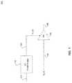
- FIG. 2is an example that illustrates the effect of timing misalignment between the PA supply voltage and the radio frequency (RF) input signal to the PA.
- RFradio frequency
- FIG. 3illustrates an example RF transmitter according to an embodiment of the present invention.
- FIG. 4illustrates an example early-late discriminator according to an embodiment of the present invention.
- FIG. 5illustrates an example output produced by an early-late discriminator for an OFDM signal, according to an embodiment of the present invention.
- FIG. 6is another example RF transmitter according to an embodiment of the present invention.
- FIG. 7is a process flowchart of a method for aligning a supply voltage signal applied to a PA with a RF output signal of the PA in a wireless device, according to an embodiment of the present invention.
- FIG. 1illustrates an example power amplifier (PA) 102 according to an embodiment of the present invention.
- PA 102may be part of a transmit path of a wireless transceiver device, for example.
- PA 102receives a radio frequency (RF) input signal 104 and generates a RF output signal 106 .
- RF input signal 104is typically generated by up-converting a complex (having in-phase (I) and quadrature (Q) components) baseband transmit signal (not shown in FIG. 1 ) to RF.
- the transmit signalis typically produced by a baseband processor (not shown in FIG. 1 ) of the wireless device to generate a desired output waveform at RF output signal 106 .
- PA 102receives a supply voltage 108 from an envelope tracking (ET) power supply 110 .
- ET power supply 110generates PA supply voltage 108 based on an ET signal 112 .
- ET signal 112is generated by the baseband processor or an RF transceiver, and has a known relationship to the transmit signal or, correspondingly, the desired output waveform.
- ET signal 112is related to the envelope (e.g., scaled and/or offset version of the envelope) of the desired transmit signal.
- ET power supply 110dynamically regulates PA supply voltage 108 according to the desired output waveform.
- PA 102By having PA supply voltage 108 track the envelope of the desired transmit signal, PA 102 is supplied with just as much voltage as instantaneously necessary to produce the desired output waveform. As such, the power efficiency of PA 102 can be significantly enhanced. Accordingly, however, there is a need to align PA supply voltage 108 with RF input signal 104 (or, correspondingly, RF output signal 106 ) so that the instantaneous value of PA supply voltage 108 corresponds to the instantaneous desired output power of RF output signal 106 to be produced by PA 102 .
- FIG. 2is an example 200 that illustrates the effect of timing misalignment between the (envelope tracking) supply voltage and the desired RF output signal of a PA.
- waveform 206represents the desired RF output signal of the PA in the time domain.
- RF output signal 206may be, for example and without limitation, a WiMAX (Worldwide Interoperability for Microwave Access) or a LTE (Long Term Evolution) waveform, with a high peak to average power ratio (PAPR).
- WiMAXWorldwide Interoperability for Microwave Access
- LTELong Term Evolution
- Supply voltage curve 202represents an ideal PA supply voltage that tracks waveform 206 , so that at any time instant the PA is provided with the necessary and sufficient voltage to produce (without non-linear distortion) the desired output power of the desired RF output signal. Accordingly, as shown in FIG. 2 , supply voltage 202 is time aligned with waveform 206 .
- supply voltage 202may be such that the PA is provided a small headroom (typically few hundred milliVolts) above what is needed to maintain linearity of waveform 206 .
- This headroomaccounts for any temperature, process, or load impedance variations that may affect the performance of the PA. As such, the power dissipation of the PA is reduced, and, consequently, its power efficiency is increased.
- Supply voltage curve 204represents an actual PA supply voltage in case of a timing misalignment between the envelope tracking PA supply voltage and the desired RF output signal of the PA.
- Time misalignment between the PA supply voltage and the RF output signal of the PAmay be due to a variety of reasons, including temperature, process, and part to part variations.
- supply voltage 204is time shifted by an amount “ ⁇ t” relative to supply voltage 202 , and hence is time misaligned with waveform 206 .
- supply voltage 204may be, at certain time instants, below what is necessary to produce the instantaneous desired output power of waveform 206 .
- the gain of the PAsags, resulting in clipping/distortion in the desired RF output signal of the PA and increased unwanted out-of-band emissions by the PA.
- Embodiments of the present inventionprovide systems and methods for aligning the supply voltage signal applied to a power amplifier (PA) with the radio frequency (RF) output signal of the PA in a wireless device.
- the RF output signalis generated by applying a transmit signal to a transmit path of the wireless device.
- the supply voltageis generated by applying an envelope tracking (ET) signal, based on the transmit signal, to an envelope tracking (ET) path of the wireless device.
- ETDenvelope tracking
- Embodimentsoperate by estimating the delays of the ET path and the transmit path, and then controlling a relative delay between the transmit signal and the ET signal accordingly.
- estimation of the delays of the ET path and the transmit pathis done by correlating respective signals of each path.
- example embodimentswill be provided. These example embodiments are provided for the purpose of illustration and are not limiting. Embodiments will be described with reference to an example transmitter having a particular architecture. Specifically, the example transmitter uses a receiver feedback path and an envelope tracking PA supply. However, embodiments are not limited to this example transmitter, and can be extended to other transmitter architectures as would be understood by a person of skill in the art based on the teachings herein.
- FIG. 3illustrates an example RF transmitter 300 according to an embodiment of the present invention.
- Example transmitter 300can be used to perform embodiments of the present invention.
- transmitter 300may include more components than shown in FIG. 3 , which are omitted herein for the purpose of simplification.
- example transmitter 300includes a digital module 302 ; a transmit path, including delay match module 338 , digital-to-analog converters (DACs) 340 a - b , filtering and up-conversion module 306 , and PA 310 ; an antenna 320 ; a Cartesian feedback path, including directional coupler 322 and down-conversion module 326 ; an envelope tracking (ET) path, including envelope compensation module 346 , DAC 348 , buffer module 350 , impedance network 352 , and power supply 314 .
- DACsdigital-to-analog converters
- transmitter 300includes, between digital module 302 and the ET path, a delay match module 342 and an envelope generator module 344 . Further, transmitter 300 includes a transmit statistics calculator module 316 . As input interfaces to transmit statistics calculator module 316 , transmitter 300 includes a multiplexer 354 , and a feedback interface path, comprised of multiplexers 334 a - b , filters 336 a - b , and analog-to-digital converters (ADCs) 330 a.
- ADCsanalog-to-digital converters
- Digital module 302which may be a baseband processor, generates digital in-phase (I) and quadrature-phase (Q) signals 304 a and 304 b based on an input signal to be transmitted. Signals 304 a - b represent the transmit signal. Digital module 302 simultaneously provides signals 304 a - b to delay match module 342 , delay match module 338 , and multiplexer 354 . In an embodiment, digital module 302 may pre-distort I and Q signals 304 a and 304 b to compensate for non-linearities in module 306 and PA 310 . In embodiments, digital module 302 may be implemented using hardware and/or software components.
- delay match 338passes signals 304 a - b , optionally after introducing a determined delay as further described below, to DACs 304 a - b .
- DACs 304 a - bconvert signals 304 a - b , respectively, from digital to analog, and provide the analog converted signals to filtering and up-conversion module 306 .
- Filtering and up-conversion module 306performs filtering (e.g., interpolation filtering) and frequency up-conversion on the analog signals, and then sums the resulting signals to generate RF signal 308 .
- PA 310receives RF signal 308 from filtering and up-conversion module 306 , and power amplifies RF signal 308 to generate an RF output signal 318 for transmission by antenna 320 .
- PA 310receives a supply voltage 312 from power supply 314 .
- power supply 314is an envelope tracking (ET) power supply that generates supply voltage 312 based on an envelope tracking signal.
- the ET signalhas a known relationship to the transmit signal, or, correspondingly, the desired output waveform of RF transmitter 300 .
- power supply 314dynamically regulates PA supply voltage 312 according to the instantaneous power level of the desired output waveform, thereby allowing PA 310 to operate at high power efficiency.
- PA 310includes a field-effect transistor (FET), and supply voltage 312 is applied to a drain terminal of the FET.
- FETfield-effect transistor
- the transmit signal(I and Q signals 304 a and 304 b ) is used to generate an ET signal, which then is applied to the ET path.
- I and Q signals 304 a - bare passed through delay match module 342 and then applied to envelope generator module 344 to produce ET signal 356 .
- Envelope generator module 344computes the envelope or magnitude (
- Signal 356is then applied to envelope compensation module 346 , which applies an appropriate compensation (e.g., scaling and/or offsetting) to ET signal 356 , to produce a compensated ET signal 358 .
- Signal 358is then converted from digital to analog using DAC 348 , and the analog switch is provided via signals 360 a - b to power supply 314 , after being applied to buffer 350 and impedance network 352 .
- Power supply 314uses signals 360 a - b to generate PA supply voltage 312 .
- supply voltage 312tracks the envelope of the desired transmit signal, and PA 310 is supplied with just as much voltage as instantaneously necessary to produce the desired output waveform. Accordingly, the power efficiency of PA 102 is greatly enhanced.
- PA supply voltage 312may be, at certain time instants, below what is necessary to produce the instantaneous desired output power of RF output signal 318 .
- the gain of PA 310sags, resulting in clipping/distortion in the desired RF output signal and increased unwanted out-of-band emissions by transmitter 300 .
- impedance network 352may introduce some delay uncertainty.
- impedance network 352is comprised of parasitic elements, which introduce a frequency dependent phase shift. As such, the delay of the ET path may vary during operation, precluding solutions based on a priori characterization and measurement of the transmit and ET paths delays.
- Embodimentsprovide systems and methods for aligning PA supply voltage Signal 312 with radio frequency (RF) output signal 308 of PA 310 .
- Embodimentsinclude estimating the delays of the ET path and the transmit path, and then controlling a relative delay between the transmit signal and the ET signal accordingly.
- the alignment processis performed during the operation of the RE transmitter, at periodic intervals, for example.
- estimation of the delays of the ET path and the transmit pathis done by correlating respective signals of each path, as further described below.
- the alignment processin an embodiment, is enabled by the Cartesian feedback path, which includes directional coupler 322 and down-conversion module 326 , the feedback interface path, which includes multiplexers 334 a - b , filters 336 a - b , and analog-to-digital converters (ADCs) 330 a , and transmit statistics calculator 316 .
- Cartesian feedback pathwhich includes directional coupler 322 and down-conversion module 326
- the feedback interface pathwhich includes multiplexers 334 a - b , filters 336 a - b , and analog-to-digital converters (ADCs) 330 a
- ADCsanalog-to-digital converters
- directional coupler 322is coupled to the output of PA 310 so as to receive output signal 318 of PA 310 and generate a RF signal 324 .
- a controllable switch 336 within coupler 322allows either a forward coupled port or a reverse coupled port of coupler 322 to be sampled.
- directional coupler 322can be used to measure either the forward or reflected signal components (both amplitude and phase) present in output signal 318 of PA 210 .
- directional coupler 322is controlled so as to measure the forward signal components at the output of PA 310 , from which a feedback signal is generated.
- RF signal 324is provided to down-conversion module 326 , which frequency down-converts RF signal 324 and generates baseband analog I and Q signals 328 a and 328 b .
- I and Q signals 328 a - brepresent the feedback signal.
- I and Q signals 328 a - bare provided, respectively, to multiplexers 334 a and 334 b of the feedback interface path.
- I and Q signals 328 a - bare passed through respective filters 336 a - b and then converted from analog to digital by ADCs 330 a - b , respectively.
- the resulting digital signals 332 a - bare provided to transmit statistics calculator 316 .
- the delay of the ET pathis estimated by correlating supply voltage 312 applied to the PA with ET signal 358 .
- an output node 362 of power supply 314having substantially identical voltage and delay characteristics as supply voltage 312 , is coupled via the feedback interface path to transmit statistics calculator 316 .
- ET signal 358is coupled via multiplexer 354 and signal 364 to transmit statistics calculator 316 .
- the ET signalis coupled before envelope compensation at node 356 of the ET path.
- Transmit statistics calculator 316correlates supply voltage 312 and ET signal 358 to estimate the delay of the ET path. In an embodiment, this includes delaying the ET signal by a delay amount to produce a delayed ET signal; correlating the supply voltage with the delayed ET signal to generate a correlation product.
- the correlation productmay include a correlation (over a plurality of offsets) between the supply voltage and the delayed ET signal. The delay amount is then adjusted and the correlation repeated, until the correlation product is maximized. The delay amount that maximizes the correlation product represents the estimate of the delay of the ET path.
- the delay amountis introduced using a delay matching circuit, for example, which may be inside or outside transmit statistics calculator 316 .
- the correlationis maximized when it results in a maximum value for zero offset between the correlated signals.
- the correlationis performed using an early-late discriminator module (not shown in FIG. 3 ), which is further described below in FIG. 4 .
- the zero offset correlationis maximized and the early-minus-late correlation is minimized.
- the delay of the transmit pathis estimated by correlating the feedback signal (I and Q signals 328 a - b ) with the transmit signal (I and Q signals 304 a - b ). Accordingly, I and Q signals 328 a - b are coupled to transmit statistics calculator 316 , by the feedback interface path, to generate digital signals 332 a - b . Concurrently, via multiplexer 354 and signal 364 (which may include more than one signal), I and Q signals 304 a - b are coupled to transmit statistics calculator 316 . The same correlation process, as described above with respect to the supply voltage and ET signal, may be used to correlate the feedback signal and the transmit signal to estimate the delay of the transmit path.
- the estimated delay of the transmit pathis an estimate of the delay of the concatenated transmit path and feedback path.
- the feedback path(which includes, directional coupler 322 and down-conversion module 326 ) includes broadband circuitry that introduces very small delay (which can be calibrated or ignored).
- the delay estimate of the transmit pathcan be further refined by subtracting from it any delay due to the feedback path, thus resulting in a better estimate of the transmit path delay.
- the feedback path delaycan be characterized a priori, for example.
- the feedback interface path(multiplexers 334 a - b , filters 336 a - b , and ADCs 330 a - b ) is common to both estimate calculations of the transmit path and the ET path, any delay associated with it can be ignored.
- a delay difference between the transmit path and the ET pathcan be computed. This delay difference is then used to control a relative delay between the transmit signal and the ET signal to align PA supply voltage 312 and RF output signal 318 .
- the relative delay between the transmit signal and the ET signalcan be controlled using one or both of delay match modules 338 and 342 . In an embodiment, the relative delay between the transmit signal and the ET signal is adjusted to bring the estimated delay difference between the transmit path and the ET path to zero.
- the delay of power supply 314can be determined by estimating, using the same process described above, the delay in the ET path up to the input of power supply 314 . This delay estimate is then subtracted from the delay estimate of the ET path to determine the delay of power supply 314 . Accordingly, input signals 360 a and 360 b of power supply 314 are coupled, via the feedback interface path, to transmit statistics calculator 316 , simultaneously with the ET signal. The signals are then correlated as described above.
- the delay of power supply 314is expected to be the largest delay component of the ET path. Accordingly, by estimating the power supply delay, the estimate can be used to calibrate the relative delay between the transmit path and the ET path accordingly. Subsequently, any differences in delay between the two paths will be due to temperature or process variations, and can be handled using small infrequent adjustments of the relative delay.
- FIG. 4illustrates an example early-late discriminator module 400 according to an embodiment of the present invention.
- Discriminator module 400may be used in embodiments to perform the correlations between the PA supply voltage and the ET signal and/or between the transmit signal and the feedback signal as described above.
- Discriminator module 400may be fully or partly integrated within transmit statistics calculator 316 of example RF transceiver 300 .
- Discriminator module 400includes a delay matching circuit 406 , delay elements 408 and 410 , a summing module 418 , multipliers 422 and 424 , and accumulator modules 426 and 432 .
- Discriminator module 400receives input signals x(k) 402 and y(k) 404 .
- Input signals x(k) 402 and y(k) 404may be the ET signal and the PA supply voltage, respectively, or, the transmit signal and the feedback signal, respectively.
- discriminator module 400generates early, prompt, and late versions 412 , 414 , and 416 , respectively, of input signal x(k) 402 using delay matching circuit 406 and delay elements 408 and 410 . Then, using multiplier 422 , discriminator module 400 correlates the prompt version 414 of input signal x(k) 402 with input signal y(k) 404 . Typically, the correlation involves correlating a number of samples of signal 414 with a corresponding number of samples of input signal y(k) 404 . The correlation product is accumulated using accumulator module 426 to generate a prompt correlation accumulation 430 .
- discriminator module 400uses summing module 418 to generate a difference 420 between the early and late versions 412 and 416 of input signal x(k).
- the difference 420is correlated using multiplier 424 with input signal y(k) 404 .
- the correlation productis accumulated using accumulator module 428 to generate an early-minus-late correlation accumulation 432 .
- the output of discriminator 400consisting of prompt correlation accumulation 430 and/or early-minus-late correlation accumulation 432 , is observed, as the delay amount introduced by delay matching circuit 406 is varied.
- FIG. 5illustrates an example output 500 of early-late discriminator module 400 according to an embodiment of the present invention.
- Example output 500shows the early-minus-late correlation accumulation 430 resulting from a delay amount of delay matching circuit 406 that closely estimates the delay between input signals x(k) 402 and y(k) 404 .
- the early-minus-late accumulationis substantially equal to zero, indicating a maximum correlation between the input signals.
- the prompt accumulation(not shown in FIG. 5 ) will have a maximum value.
- FIG. 6is another example RF transmitter 600 according to an embodiment of the present invention.
- Example transmitter 600is similar to example transmitter 300 described above.
- example transmitter 600implements an early-late discriminator, as described above in FIGS. 4 and 5 .
- example transmitter 600includes a delay match module 368 and delay elements 370 and 372 . These elements correspond respectively, for example, to delay matching circuit 406 and delay elements 408 and 410 in discriminator module 400 described above.
- Delay match element 368can be used to produce and adjust the delay amount for the correlations performed in transmit statistics calculator 316 . The value of the delay amount in delay match element 368 that maximizes the correlation (for zero offset) between the signals being correlated corresponds to the path delay being estimated.
- FIG. 7is a process flowchart 700 of a method for aligning a supply voltage signal applied to a PA with a RF output signal of the PA in a wireless device, according to an embodiment of the present invention.
- the RF output signal of the PAis generated by applying a transmit signal (e.g., digital complex baseband signal) to a transmit path, including the PA, of the wireless device.
- the supply voltage signalis generated by applying an envelope tracking (ET) signal to an ET path of the wireless device.
- ETenvelope tracking
- the ET signalis based on the transmit signal.
- the ET signalis related to the envelope of the transmit signal.
- process 700begins in step 702 , which includes correlating the supply voltage signal applied to the PA with the ET signal to estimate a first delay of the ET path of a wireless device.
- correlating the supply voltage with the ET signalincludes delaying the ET signal by a delay amount to produce a delayed ET signal; correlating the supply voltage signal with the delayed ET signal to generate a correlation product; and adjusting the delay amount until the correlation product is maximized.
- step 702is performed using an early-late discriminator module. Accordingly, step 702 further includes generating an early, prompt, and late versions of the delayed ET signal, where the early, prompt, and late versions of the ET signal have respective delays relative to the ET signal; correlating the supply voltage signal with the prompt version of the delayed ET signal to generate a prompt correlation value; and correlating the supply voltage with a difference of the early and late versions of the delay ET signal to generate an early-minus-late correlation value. Subsequently, the delay amount is adjusted until the early-minus-late correlation value is substantially equal to zero and/or the prompt correlation value is at a maximum value. This indicates that the correlation product between the supply voltage and the delayed ET signal is maximized. The delay amount for which the correlation product between the supply voltage signal and the delayed ET signal is maximized represents the estimated delay of the ET path.
- Process 700continues at step 704 , which includes correlating a feedback signal, generated by applying the RF output signal of the PA to a feedback path of the wireless device, with a transmit signal to estimate a second delay of a transmit path of the wireless device.
- the feedback signalis a complex baseband signal generated by frequency down-converting and digitizing the RF output signal using the feedback path.
- Correlating the feedback signal with the transmit signalcan be performed using the same process described above for correlating the supply voltage signal applied to the PA with the ET signal.
- the same system modulee.g., early-late discriminator module
- steps 702 and 704may be performed simultaneously or in an opposite order than described here.
- process 700proceeds to step 706 , which includes estimating a delay difference between the transmit path and the ET path based on the first delay and the second delay.
- the delay difference between the transmit path and the ET pathis equal to the difference between the first delay and the second delay.
- step 706further includes estimating a delay of the feedback path; and compensating the second delay of the transmit path based on the delay of the feedback path.
- the second delay(estimated in step 704 ) is an estimate of the delay of the concatenated transmit path and feedback path.
- the feedback path(which includes, for example, a directional coupler and a down-conversion module) includes broadband circuitry that introduces very small delay (which can be calibrated or ignored). For better accuracy, however, the second delay estimate can be further refined by subtracting from it any delay due to the feedback path, thus resulting in a better estimate of the transmit path delay.
- process 700includes controlling a relative delay between the transmit signal and the ET signal based on the estimated delay difference to align the supply voltage signal applied to the PA and the RF output signal of the wireless device.
- step 708includes controlling the relative delay between the transmit signal and the ET signal to bring the estimated delay difference to zero.
- step 708is performed by adjusting a delay element in the transmit path or the ET path to control the relative delay between the transmit signal and the ET signal, as desired.
Landscapes
- Engineering & Computer Science (AREA)
- Power Engineering (AREA)
- Computer Networks & Wireless Communication (AREA)
- Signal Processing (AREA)
- Physics & Mathematics (AREA)
- Nonlinear Science (AREA)
- Transmitters (AREA)
Abstract
Description
Claims (21)
Priority Applications (1)
| Application Number | Priority Date | Filing Date | Title |
|---|---|---|---|
| US13/491,184US9066368B2 (en) | 2011-06-08 | 2012-06-07 | Method of calibrating the delay of an envelope tracking signal |
Applications Claiming Priority (3)
| Application Number | Priority Date | Filing Date | Title |
|---|---|---|---|
| US201161494846P | 2011-06-08 | 2011-06-08 | |
| US201261611723P | 2012-03-16 | 2012-03-16 | |
| US13/491,184US9066368B2 (en) | 2011-06-08 | 2012-06-07 | Method of calibrating the delay of an envelope tracking signal |
Publications (2)
| Publication Number | Publication Date |
|---|---|
| US20130109441A1 US20130109441A1 (en) | 2013-05-02 |
| US9066368B2true US9066368B2 (en) | 2015-06-23 |
Family
ID=47296477
Family Applications (1)
| Application Number | Title | Priority Date | Filing Date |
|---|---|---|---|
| US13/491,184Active2033-02-19US9066368B2 (en) | 2011-06-08 | 2012-06-07 | Method of calibrating the delay of an envelope tracking signal |
Country Status (3)
| Country | Link |
|---|---|
| US (1) | US9066368B2 (en) |
| EP (1) | EP2719086A4 (en) |
| WO (1) | WO2012170831A1 (en) |
Cited By (10)
| Publication number | Priority date | Publication date | Assignee | Title |
|---|---|---|---|---|
| US20160050629A1 (en)* | 2014-08-13 | 2016-02-18 | Skyworks Solutions, Inc. | Apparatus and methods for wideband envelope tracking systems |
| US9413299B2 (en)* | 2013-07-18 | 2016-08-09 | Intel Deutschland Gmbh | Systems and methods utilizing adaptive envelope tracking |
| US9530719B2 (en) | 2014-06-13 | 2016-12-27 | Skyworks Solutions, Inc. | Direct die solder of gallium arsenide integrated circuit dies and methods of manufacturing gallium arsenide wafers |
| US20170353202A1 (en)* | 2016-06-06 | 2017-12-07 | Airbus Ds Slc | Device and method for processing a signal received by a receiver disrupted by a transmitter |
| US10103693B2 (en) | 2015-09-30 | 2018-10-16 | Skyworks Solutions, Inc. | Power amplifier linearization system and method |
| US10110169B2 (en) | 2016-09-14 | 2018-10-23 | Skyworks Solutions, Inc. | Apparatus and methods for envelope tracking systems with automatic mode selection |
| US10236831B2 (en) | 2017-05-12 | 2019-03-19 | Skyworks Solutions, Inc. | Envelope trackers providing compensation for power amplifier output load variation |
| US10516368B2 (en) | 2017-06-21 | 2019-12-24 | Skyworks Solutions, Inc. | Fast envelope tracking systems for power amplifiers |
| US10615757B2 (en) | 2017-06-21 | 2020-04-07 | Skyworks Solutions, Inc. | Wide bandwidth envelope trackers |
| US11581964B2 (en) | 2020-07-07 | 2023-02-14 | Samsung Electronics Co., Ltd. | Communication apparatus for supporting envelope tracking modulation and envelope delay optimization method |
Families Citing this family (10)
| Publication number | Priority date | Publication date | Assignee | Title |
|---|---|---|---|---|
| CN104620509B (en) | 2012-03-04 | 2017-05-10 | 匡坦斯公司 | Envelope tracking power amplifier system with delay calibration and time calibration method |
| US9281852B2 (en) | 2013-01-04 | 2016-03-08 | Marvell World Trade Ltd. | Method and apparatus for calibrating time alignment |
| KR102179318B1 (en) | 2013-03-14 | 2020-11-16 | 퀀탄스, 인코포레이티드 | Et system with adjustment for noise |
| WO2014151777A1 (en) | 2013-03-15 | 2014-09-25 | Quantance, Inc. | Envelope tracking system with internal power amplifier characterization |
| JP6264778B2 (en)* | 2013-08-15 | 2018-01-24 | 富士通株式会社 | Wireless communication circuit and wireless communication device |
| DE102014104371A1 (en)* | 2014-03-28 | 2015-10-01 | Intel IP Corporation | An apparatus and method for amplifying a transmit signal or for determining values of a delay control parameter |
| DE102014104372A1 (en) | 2014-03-28 | 2015-10-01 | Intel IP Corporation | An apparatus and method for amplifying a transmission signal |
| US9520845B2 (en) | 2014-11-14 | 2016-12-13 | Microsoft Technology Licensing, Llc | Supply modulation for radio frequency power amplification |
| US9571135B2 (en)* | 2015-03-20 | 2017-02-14 | Intel IP Corporation | Adjusting power amplifier stimuli based on output signals |
| US10361744B1 (en)* | 2018-03-05 | 2019-07-23 | Qorvo Us, Inc. | Transceiver circuit and related radio frequency circuit |
Citations (19)
| Publication number | Priority date | Publication date | Assignee | Title |
|---|---|---|---|---|
| US6407634B1 (en) | 2000-06-16 | 2002-06-18 | Motorola, Inc. | Linear envelope tracking RF power amplifier with adaptive analog signal processing |
| US20020101912A1 (en)* | 1999-12-01 | 2002-08-01 | Phelts Robert Eric | Multipath and tracking error reduction method for spread-spectrum receivers |
| US6792059B2 (en)* | 2000-11-30 | 2004-09-14 | Trw Inc. | Early/on-time/late gate bit synchronizer |
| US20050110562A1 (en)* | 2003-11-20 | 2005-05-26 | Ian Robinson | Variable supply amplifier system |
| US20060199553A1 (en) | 2005-03-07 | 2006-09-07 | Andrew Corporation | Integrated transceiver with envelope tracking |
| US7190709B2 (en)* | 2002-11-04 | 2007-03-13 | Advanced Micro Devices, Inc. | Early-late correlation for timing error correction in data communication receivers |
| US20070121708A1 (en)* | 2005-11-28 | 2007-05-31 | Honeywell International, Inc. | Discriminator function for GPS code alignment |
| US20090004981A1 (en)* | 2007-06-27 | 2009-01-01 | Texas Instruments Incorporated | High efficiency digital transmitter incorporating switching power supply and linear power amplifier |
| US20090097591A1 (en) | 2007-10-10 | 2009-04-16 | Samsung Electronics Co., Ltd. | Apparatus and method for envelope tracking power amplification in wireless communication system |
| US20090302938A1 (en)* | 2005-12-30 | 2009-12-10 | D2Audio Corporation | Low delay corrector |
| US20100233977A1 (en)* | 2006-03-30 | 2010-09-16 | Nxp B.V. | Multi-mode radio transmitters and a method of their operation |
| US20110058601A1 (en) | 2009-09-07 | 2011-03-10 | Samsung Electronics Co., Ltd. | Apparatus and method for envelope tracking power amplifier in wireless communication system |
| US8094764B2 (en)* | 2008-12-03 | 2012-01-10 | Bae Systems Information And Electronic Systems Integration Inc. | Variable time delay control structure for channel matching |
| US20120056677A1 (en)* | 2010-09-02 | 2012-03-08 | Samsung Electronics Co., Ltd. | Apparatus and method for a tunable multi-mode multi-band power amplifier module |
| US20120202435A1 (en)* | 2011-02-07 | 2012-08-09 | Nam Yun Kim | Method and apparatus for controlling wireless power transmission and reception, and wireless power transmission system |
| US20130034139A1 (en)* | 2011-02-07 | 2013-02-07 | Rf Micro Devices, Inc. | Group delay calibration method for power amplifier envelope tracking |
| US20130109442A1 (en)* | 2011-06-08 | 2013-05-02 | Sriraman Dakshinamurthy | Methods and Systems for Pre-Emphasis of an Envelope Tracking Power Amplifier Supply Voltage |
| US20130231069A1 (en)* | 2012-03-04 | 2013-09-05 | Quantance, Inc. | Envelope Tracking Power Amplifier System with Delay Calibration |
| US8571154B1 (en)* | 2012-04-19 | 2013-10-29 | Bae Systems Information And Electronic Systems Integration Inc. | Control interval expansion of variable time delay control structure for channel matching |
- 2012
- 2012-06-07USUS13/491,184patent/US9066368B2/enactiveActive
- 2012-06-08EPEP12726713.6Apatent/EP2719086A4/ennot_activeWithdrawn
- 2012-06-08WOPCT/US2012/041573patent/WO2012170831A1/enactiveApplication Filing
Patent Citations (24)
| Publication number | Priority date | Publication date | Assignee | Title |
|---|---|---|---|---|
| US20020101912A1 (en)* | 1999-12-01 | 2002-08-01 | Phelts Robert Eric | Multipath and tracking error reduction method for spread-spectrum receivers |
| US6407634B1 (en) | 2000-06-16 | 2002-06-18 | Motorola, Inc. | Linear envelope tracking RF power amplifier with adaptive analog signal processing |
| US6792059B2 (en)* | 2000-11-30 | 2004-09-14 | Trw Inc. | Early/on-time/late gate bit synchronizer |
| US7190709B2 (en)* | 2002-11-04 | 2007-03-13 | Advanced Micro Devices, Inc. | Early-late correlation for timing error correction in data communication receivers |
| US20050110562A1 (en)* | 2003-11-20 | 2005-05-26 | Ian Robinson | Variable supply amplifier system |
| US7026868B2 (en) | 2003-11-20 | 2006-04-11 | Northrop Grumman Corporation | Variable supply amplifier system |
| US20060199553A1 (en) | 2005-03-07 | 2006-09-07 | Andrew Corporation | Integrated transceiver with envelope tracking |
| US20090045872A1 (en)* | 2005-03-07 | 2009-02-19 | Peter Blakeborough Kenington | Integrated transceiver with envelope tracking |
| US20070121708A1 (en)* | 2005-11-28 | 2007-05-31 | Honeywell International, Inc. | Discriminator function for GPS code alignment |
| US20090302938A1 (en)* | 2005-12-30 | 2009-12-10 | D2Audio Corporation | Low delay corrector |
| US20100233977A1 (en)* | 2006-03-30 | 2010-09-16 | Nxp B.V. | Multi-mode radio transmitters and a method of their operation |
| US20090004981A1 (en)* | 2007-06-27 | 2009-01-01 | Texas Instruments Incorporated | High efficiency digital transmitter incorporating switching power supply and linear power amplifier |
| US20090097591A1 (en) | 2007-10-10 | 2009-04-16 | Samsung Electronics Co., Ltd. | Apparatus and method for envelope tracking power amplification in wireless communication system |
| US8094764B2 (en)* | 2008-12-03 | 2012-01-10 | Bae Systems Information And Electronic Systems Integration Inc. | Variable time delay control structure for channel matching |
| US8411809B2 (en)* | 2008-12-03 | 2013-04-02 | Bae Systems Information And Electronic Systems Integration Inc. | Variable time delay control structure for channel matching |
| US20110058601A1 (en) | 2009-09-07 | 2011-03-10 | Samsung Electronics Co., Ltd. | Apparatus and method for envelope tracking power amplifier in wireless communication system |
| US20120056677A1 (en)* | 2010-09-02 | 2012-03-08 | Samsung Electronics Co., Ltd. | Apparatus and method for a tunable multi-mode multi-band power amplifier module |
| US20130034139A1 (en)* | 2011-02-07 | 2013-02-07 | Rf Micro Devices, Inc. | Group delay calibration method for power amplifier envelope tracking |
| US20120202435A1 (en)* | 2011-02-07 | 2012-08-09 | Nam Yun Kim | Method and apparatus for controlling wireless power transmission and reception, and wireless power transmission system |
| US20130109442A1 (en)* | 2011-06-08 | 2013-05-02 | Sriraman Dakshinamurthy | Methods and Systems for Pre-Emphasis of an Envelope Tracking Power Amplifier Supply Voltage |
| US20130231069A1 (en)* | 2012-03-04 | 2013-09-05 | Quantance, Inc. | Envelope Tracking Power Amplifier System with Delay Calibration |
| US8718579B2 (en)* | 2012-03-04 | 2014-05-06 | Quantance, Inc. | Envelope tracking power amplifier system with delay calibration |
| US20140235185A1 (en)* | 2012-03-04 | 2014-08-21 | Quantance, Inc. | Envelope Tracking Power Amplifier System with Delay Calibration |
| US8571154B1 (en)* | 2012-04-19 | 2013-10-29 | Bae Systems Information And Electronic Systems Integration Inc. | Control interval expansion of variable time delay control structure for channel matching |
Non-Patent Citations (3)
| Title |
|---|
| International Preliminary Report on Patentability with Written Opinion directed toward related International Application No. PCT/US2012/041573, dated Dec. 10, 2013, from The International Bureau of WIPO, Geneva, Switzerland; 10 pages. |
| International Search Report for PCT Application No. PCT/US2012/041573, dated Aug. 27, 2012, 16 pages. |
| Supplementary European Search Report directed toward related EP Application No. 12726713.6, dated Nov. 3, 2014, from the European Patent Office, Munich, Germany; 3 pages. |
Cited By (23)
| Publication number | Priority date | Publication date | Assignee | Title |
|---|---|---|---|---|
| US9413299B2 (en)* | 2013-07-18 | 2016-08-09 | Intel Deutschland Gmbh | Systems and methods utilizing adaptive envelope tracking |
| US9530719B2 (en) | 2014-06-13 | 2016-12-27 | Skyworks Solutions, Inc. | Direct die solder of gallium arsenide integrated circuit dies and methods of manufacturing gallium arsenide wafers |
| US9666508B2 (en) | 2014-06-13 | 2017-05-30 | Skyworks Solutions, Inc. | Gallium arsenide devices with copper backside for direct die solder attach |
| US9876473B2 (en) | 2014-08-13 | 2018-01-23 | Skyworks Solutions, Inc. | Apparatus and methods for wideband envelope tracking |
| US9445371B2 (en)* | 2014-08-13 | 2016-09-13 | Skyworks Solutions, Inc. | Apparatus and methods for wideband envelope tracking systems |
| US20160050629A1 (en)* | 2014-08-13 | 2016-02-18 | Skyworks Solutions, Inc. | Apparatus and methods for wideband envelope tracking systems |
| US10812026B2 (en) | 2015-09-30 | 2020-10-20 | Skyworks Solutions, Inc. | Power amplifier linearization system and method |
| US10103693B2 (en) | 2015-09-30 | 2018-10-16 | Skyworks Solutions, Inc. | Power amplifier linearization system and method |
| US10381985B2 (en) | 2015-09-30 | 2019-08-13 | Skyworks Solutions, Inc. | Power amplifier linearization system and method |
| US20170353202A1 (en)* | 2016-06-06 | 2017-12-07 | Airbus Ds Slc | Device and method for processing a signal received by a receiver disrupted by a transmitter |
| US10056927B2 (en)* | 2016-06-06 | 2018-08-21 | Airbus Ds Slc | Device and method for processing a signal received by a receiver disrupted by a transmitter |
| US10110169B2 (en) | 2016-09-14 | 2018-10-23 | Skyworks Solutions, Inc. | Apparatus and methods for envelope tracking systems with automatic mode selection |
| US10454428B2 (en) | 2016-09-14 | 2019-10-22 | Skyworks Solutions, Inc. | Apparatus and methods for envelope tracking systems with automatic mode selection |
| US11595006B2 (en) | 2016-09-14 | 2023-02-28 | Skyworks Solutions, Inc. | Apparatus and methods for envelope tracking systems with automatic mode selection |
| US10873297B2 (en) | 2016-09-14 | 2020-12-22 | Skyworks Solutions, Inc. | Apparatus and methods for envelope tracking systems with automatic mode selection |
| US10236831B2 (en) | 2017-05-12 | 2019-03-19 | Skyworks Solutions, Inc. | Envelope trackers providing compensation for power amplifier output load variation |
| US10651802B2 (en) | 2017-05-12 | 2020-05-12 | Skyworks Solutions, Inc. | Envelope trackers providing compensation for power amplifier output load variation |
| US10615757B2 (en) | 2017-06-21 | 2020-04-07 | Skyworks Solutions, Inc. | Wide bandwidth envelope trackers |
| US10985711B2 (en) | 2017-06-21 | 2021-04-20 | Skyworks Solutions, Inc. | Wide bandwidth envelope trackers |
| US10985703B2 (en) | 2017-06-21 | 2021-04-20 | Skyworks Solutions, Inc. | Fast envelope tracking systems for power amplifiers |
| US11558015B2 (en) | 2017-06-21 | 2023-01-17 | Skyworks Solutions, Inc. | Fast envelope tracking systems for power amplifiers |
| US10516368B2 (en) | 2017-06-21 | 2019-12-24 | Skyworks Solutions, Inc. | Fast envelope tracking systems for power amplifiers |
| US11581964B2 (en) | 2020-07-07 | 2023-02-14 | Samsung Electronics Co., Ltd. | Communication apparatus for supporting envelope tracking modulation and envelope delay optimization method |
Also Published As
| Publication number | Publication date |
|---|---|
| EP2719086A1 (en) | 2014-04-16 |
| EP2719086A4 (en) | 2014-12-03 |
| US20130109441A1 (en) | 2013-05-02 |
| WO2012170831A1 (en) | 2012-12-13 |
Similar Documents
| Publication | Publication Date | Title |
|---|---|---|
| US9066368B2 (en) | Method of calibrating the delay of an envelope tracking signal | |
| US9692366B2 (en) | Envelope tracking path delay fine tuning and calibration | |
| EP3070839B1 (en) | Adjusting power amplifier stimuli based on output signals | |
| US7248112B2 (en) | Hybrid distortion compensation method and hybrid distortion compensation device | |
| CN100542055C (en) | Transmission circuit, wireless communication device, and timing adjustment method for transmission circuit | |
| US20160087657A1 (en) | Adaptively Controlled Pre-Distortion Circuits for RF Power Amplifiers | |
| US8326239B1 (en) | Power amplifier linearization using digital predistortion | |
| US9099966B2 (en) | Dual time alignment architecture for transmitters using EER/ET amplifiers and others | |
| US8837635B2 (en) | Controlling a transmit path based on monitored error vector magnitude (EVM) performance | |
| US9755583B2 (en) | Using fractional delay computations to improve intermodulation performance | |
| CN104584501A (en) | Method and system for aligning signals widely spaced in frequency for wideband digital predistortion in wireless communication systems | |
| US20130109442A1 (en) | Methods and Systems for Pre-Emphasis of an Envelope Tracking Power Amplifier Supply Voltage | |
| CN108347226B (en) | Envelope tracking method, system and device | |
| TW201448532A (en) | Method and apparatus for compensating IQ imbalance | |
| US10056863B2 (en) | Technique for determining a time alignment error | |
| WO2009011071A1 (en) | Amplifier device with nonlinear-distortion compensation | |
| JP4659621B2 (en) | Wireless transmitter | |
| JP7719895B2 (en) | System and method for compensating a transmit signal for charge trapping effects in a power amplifier | |
| Safari et al. | Block based predistortion for amplifier linearization in burst type mobile satellite communications | |
| EP3402098A1 (en) | Transceiver for a wireless communication system, and methods for increasing transceiver loopback calibration accuracy | |
| KR20100045630A (en) | Apparatus and method for amplifying electric power of broadband |
Legal Events
| Date | Code | Title | Description |
|---|---|---|---|
| AS | Assignment | Owner name:BROADCOM CORPORATION, CALIFORNIA Free format text:ASSIGNMENT OF ASSIGNORS INTEREST;ASSIGNORS:LORENZ, ROBERT;RANGANATHAN, SUMANT;YU, XINYU;AND OTHERS;SIGNING DATES FROM 20120726 TO 20120810;REEL/FRAME:028815/0139 | |
| STCF | Information on status: patent grant | Free format text:PATENTED CASE | |
| AS | Assignment | Owner name:BANK OF AMERICA, N.A., AS COLLATERAL AGENT, NORTH CAROLINA Free format text:PATENT SECURITY AGREEMENT;ASSIGNOR:BROADCOM CORPORATION;REEL/FRAME:037806/0001 Effective date:20160201 Owner name:BANK OF AMERICA, N.A., AS COLLATERAL AGENT, NORTH Free format text:PATENT SECURITY AGREEMENT;ASSIGNOR:BROADCOM CORPORATION;REEL/FRAME:037806/0001 Effective date:20160201 | |
| CC | Certificate of correction | ||
| AS | Assignment | Owner name:AVAGO TECHNOLOGIES GENERAL IP (SINGAPORE) PTE. LTD., SINGAPORE Free format text:ASSIGNMENT OF ASSIGNORS INTEREST;ASSIGNOR:BROADCOM CORPORATION;REEL/FRAME:041706/0001 Effective date:20170120 Owner name:AVAGO TECHNOLOGIES GENERAL IP (SINGAPORE) PTE. LTD Free format text:ASSIGNMENT OF ASSIGNORS INTEREST;ASSIGNOR:BROADCOM CORPORATION;REEL/FRAME:041706/0001 Effective date:20170120 | |
| AS | Assignment | Owner name:BROADCOM CORPORATION, CALIFORNIA Free format text:TERMINATION AND RELEASE OF SECURITY INTEREST IN PATENTS;ASSIGNOR:BANK OF AMERICA, N.A., AS COLLATERAL AGENT;REEL/FRAME:041712/0001 Effective date:20170119 | |
| AS | Assignment | Owner name:AVAGO TECHNOLOGIES INTERNATIONAL SALES PTE. LIMITE Free format text:MERGER;ASSIGNOR:AVAGO TECHNOLOGIES GENERAL IP (SINGAPORE) PTE. LTD.;REEL/FRAME:047229/0408 Effective date:20180509 | |
| AS | Assignment | Owner name:AVAGO TECHNOLOGIES INTERNATIONAL SALES PTE. LIMITE Free format text:CORRECTIVE ASSIGNMENT TO CORRECT THE EFFECTIVE DATE PREVIOUSLY RECORDED ON REEL 047229 FRAME 0408. ASSIGNOR(S) HEREBY CONFIRMS THE THE EFFECTIVE DATE IS 09/05/2018;ASSIGNOR:AVAGO TECHNOLOGIES GENERAL IP (SINGAPORE) PTE. LTD.;REEL/FRAME:047349/0001 Effective date:20180905 | |
| MAFP | Maintenance fee payment | Free format text:PAYMENT OF MAINTENANCE FEE, 4TH YEAR, LARGE ENTITY (ORIGINAL EVENT CODE: M1551); ENTITY STATUS OF PATENT OWNER: LARGE ENTITY Year of fee payment:4 | |
| AS | Assignment | Owner name:AVAGO TECHNOLOGIES INTERNATIONAL SALES PTE. LIMITE Free format text:CORRECTIVE ASSIGNMENT TO CORRECT THE PATENT NUMBER 9,385,856 TO 9,385,756 PREVIOUSLY RECORDED AT REEL: 47349 FRAME: 001. ASSIGNOR(S) HEREBY CONFIRMS THE MERGER;ASSIGNOR:AVAGO TECHNOLOGIES GENERAL IP (SINGAPORE) PTE. LTD.;REEL/FRAME:051144/0648 Effective date:20180905 | |
| MAFP | Maintenance fee payment | Free format text:PAYMENT OF MAINTENANCE FEE, 8TH YEAR, LARGE ENTITY (ORIGINAL EVENT CODE: M1552); ENTITY STATUS OF PATENT OWNER: LARGE ENTITY Year of fee payment:8 |