US9065163B1 - High frequency power combiner/divider - Google Patents
High frequency power combiner/dividerDownload PDFInfo
- Publication number
- US9065163B1 US9065163B1US13/726,073US201213726073AUS9065163B1US 9065163 B1US9065163 B1US 9065163B1US 201213726073 AUS201213726073 AUS 201213726073AUS 9065163 B1US9065163 B1US 9065163B1
- Authority
- US
- United States
- Prior art keywords
- waveguide
- hollow
- waveguides
- transmission line
- combiner
- Prior art date
- Legal status (The legal status is an assumption and is not a legal conclusion. Google has not performed a legal analysis and makes no representation as to the accuracy of the status listed.)
- Expired - Fee Related, expires
Links
Images


Classifications
- H—ELECTRICITY
- H01—ELECTRIC ELEMENTS
- H01P—WAVEGUIDES; RESONATORS, LINES, OR OTHER DEVICES OF THE WAVEGUIDE TYPE
- H01P5/00—Coupling devices of the waveguide type
- H01P5/12—Coupling devices having more than two ports
- H—ELECTRICITY
- H01—ELECTRIC ELEMENTS
- H01P—WAVEGUIDES; RESONATORS, LINES, OR OTHER DEVICES OF THE WAVEGUIDE TYPE
- H01P3/00—Waveguides; Transmission lines of the waveguide type
- H01P3/12—Hollow waveguides
- H—ELECTRICITY
- H01—ELECTRIC ELEMENTS
- H01P—WAVEGUIDES; RESONATORS, LINES, OR OTHER DEVICES OF THE WAVEGUIDE TYPE
- H01P11/00—Apparatus or processes specially adapted for manufacturing waveguides or resonators, lines, or other devices of the waveguide type
- H01P11/001—Manufacturing waveguides or transmission lines of the waveguide type
- H01P11/002—Manufacturing hollow waveguides
- H—ELECTRICITY
- H03—ELECTRONIC CIRCUITRY
- H03F—AMPLIFIERS
- H03F3/00—Amplifiers with only discharge tubes or only semiconductor devices as amplifying elements
- H03F3/189—High-frequency amplifiers, e.g. radio frequency amplifiers
- H03F3/19—High-frequency amplifiers, e.g. radio frequency amplifiers with semiconductor devices only
- H03F3/195—High-frequency amplifiers, e.g. radio frequency amplifiers with semiconductor devices only in integrated circuits
- H—ELECTRICITY
- H03—ELECTRONIC CIRCUITRY
- H03F—AMPLIFIERS
- H03F3/00—Amplifiers with only discharge tubes or only semiconductor devices as amplifying elements
- H03F3/20—Power amplifiers, e.g. Class B amplifiers, Class C amplifiers
- H03F3/21—Power amplifiers, e.g. Class B amplifiers, Class C amplifiers with semiconductor devices only
- H03F3/211—Power amplifiers, e.g. Class B amplifiers, Class C amplifiers with semiconductor devices only using a combination of several amplifiers
- H—ELECTRICITY
- H03—ELECTRONIC CIRCUITRY
- H03F—AMPLIFIERS
- H03F3/00—Amplifiers with only discharge tubes or only semiconductor devices as amplifying elements
- H03F3/60—Amplifiers in which coupling networks have distributed constants, e.g. with waveguide resonators
- H03F3/602—Combinations of several amplifiers
- H—ELECTRICITY
- H01—ELECTRIC ELEMENTS
- H01P—WAVEGUIDES; RESONATORS, LINES, OR OTHER DEVICES OF THE WAVEGUIDE TYPE
- H01P5/00—Coupling devices of the waveguide type
- H01P5/02—Coupling devices of the waveguide type with invariable factor of coupling
- H01P5/022—Transitions between lines of the same kind and shape, but with different dimensions
- H01P5/024—Transitions between lines of the same kind and shape, but with different dimensions between hollow waveguides
Definitions
- the present inventionrelates generally to radio frequency (RF) power amplifiers, and more particularly but not exclusively to high power, wideband, microwave or millimeter-wave solid state power amplifiers based on waveguide power combiner/dividers.
- RFradio frequency
- TWTtravelling wave tubes
- TWT amplifiersrequire a high voltage driver, such as an electronic power conditioner, that in turn necessitates additional complex accessory circuits and involves high voltage risk.
- a high voltage driversuch as an electronic power conditioner
- TWT amplifiersare normally backed off from their saturated output power or additional linearization circuits are added, and linearization circuitry usually results in a dramatic increase in the system complexity and cost.
- vacuum tubes, including TWT'stypically require operation at a designed output power; however, atmospheric variation may require a source that can change its power level based on conditions in the transmit/receive path.
- a solid state power amplifier (SSPA) module for satellite, terrestrial, aerospace, and/or unmanned aerial vehicle (UAV) applicationsmay require compact size and light weight. Further, such applications may require an SSPA module that has more power than one monolithic microwave integrated circuit (MMIC) chip can provide.
- MMICmonolithic microwave integrated circuit
- the SSPAcontinues to advance into the territory traditionally dominated by the vacuum tube amplifier in terms of increased frequency, power, and bandwidth as the MMIC chips to support them continue to advance, for example with advances in GaN and GaAs semiconductor technology.
- Existing SSPA designsare based on power combiners, such as radial combiners, but they sometimes tend to be bulky, heavy, and/or require complex machining.
- split block waveguide structure/combinerscan be used to reduce machining complexity, the SSPA may suffer from both leakage problems and joining problems.
- This problem of building a waveguide from separate parts that must be joined, and general insertion and return loss problems over the bandwidth required,can be compounded or increased by the tolerances and structural accuracy needed to properly guide the propagating waves in a hollow waveguide construction.
- integration of conductive signal line based waveguides, such as microstrip, CPW (Co-Planar Waveguide), or coaxis additionally complicated due to tolerances and alignment that may be required.
- SSPA designsmay include a large number of components that must be manually assembled and tuned after assembly.
- Many individual pieces of existing SSPA designsrequire complex machining, such as, for example, extremely high precision milling, wire Electric Discharge Machining (EDM) and/or laser processes which lead to relatively high manufacturing costs and challenges in the part integration and bonding to produce a device with sufficiently good electromagnetic properties, for example, in terms of accumulative insertion and/or return loss.
- EDMElectrodet Machining
- required machining tolerances at high frequenciesmake mass production difficult because every SSPA may have to be manually assembled and tuned to compensate for the manufacturing tolerances. Accordingly, there may be a need for a solid state high power amplifier module which has more desirable cost, size, precision forming, precision assembly, and/or reliability attributes and that readily lends itself to scalable, and cost-effective, manufacturing methods.
- the present inventionmay relate to a microwave or millimeter-wave solid state high power amplifier such as those that are used in radar and satellite communication systems.
- An exemplary waveguide device configurationmay contain at least one port to accept a transmission line mode of at least one signal line and to convert it to at least one hollow core waveguide mode within at least one hollow core waveguide combiner.
- the hollow core waveguide combinermay include one or more branching sections that divide or combine electromagnetic signals, which sections may meet to divide or combine energy and power from two hollow core waveguide branches.
- Exemplary devicesmay include precision electrical and/or mechanical features for the conversion between a transmission line mode and hollow waveguide radiation mode(s).
- a waveguide power combiner/divider of the present inventionmay include a plurality of hollow waveguides having a hollow core configured to support at least one radiation mode therein.
- the waveguidesmay include first and second ends with the second ends in communication with one another to permit communication of radiation modes therebetween. The second ends may be joined in way to allow or form a common output port for the 2 or more waveguide first ends.
- a plurality of transmission line waveguides having a center conductor transmission line disposed thereinmay also be provided.
- Each of the transmission line waveguidesfor example coaxial transmission line waveguides, may include an electromagnetic end launcher operably connected to respective first ends of the hollow waveguides.
- Each electromagnetic end launchermay include an elongated center conductor end portion that extends into the hollow core of the hollow waveguide.
- a plurality of ground postsmay also be provided, each of which may be disposed at a respective end launcher in electrical communication with the center conductor and a wall of the hollow waveguide to ground the end launcher to the hollow waveguide wall.
- the electrical and/or mechanical featuresmay be formed in a build sequence monolithically or directly, for example using an additive microfabrication process, such as the PolyStrata® process by Nuvotronics, LLC.
- an additive microfabrication processsuch as the PolyStrata® process by Nuvotronics, LLC.
- the later alignment and assembly for transition between a plurality of signal line or transmission line based waveguides, said electromagnetic end launchers, and hollow core waveguidesis not required.
- these relationshipsare determined image-wise, for example by application of successive planar photo-patterns or precision machine defined patterns.
- the present inventionmay provide a novel power combining structure based on a microfabrication process which permits the precision manufacturing of small parts, typically on a wafer, substrate, grid-level, or batch level.
- Other precision forming techniquessuch as, for example, precision milling, stereolithography, solid printing, or injection molding, may be used to create either all, or a part of, the novel power combining structures disclosed herein.
- power combining structures of the present inventionmay include an air-coax input power divider; pre-driver, driver, sub-amplifier modules (which may themselves include an air-coax divider and combiner, phase shifters, filters and/or linearizers), a microfabricated output waveguide combiner; and/or, an air-coax or waveguide output.
- the power amplifiermay be made in a modular format allowing building blocks that can be independently tested and which aid in scalable products that reuse similar or identical components in their architecture.
- the relationships for the mechanical elements which govern the electromagnetic propertiesmay be addressed during the forming process.
- precision integration of these componentsmay allow them to be assembled with the necessary tolerances and precision for an intended application.
- the waveguide combiner portion of the SSPAmay be fed by a number of amplifier modules (or “sub-modules”) feeding each input port and the respective input port end launcher of said hollow core waveguide power combiner.
- Each of these amplifier modulesmay have multiple MMIC chips (e.g., such as 2 chips, 4 chips or 8 chips using a 2-way or 4-way or 8-way Wilkinson or Gysel sub-combiner).
- MMIC chipse.g., such as 2 chips, 4 chips or 8 chips using a 2-way or 4-way or 8-way Wilkinson or Gysel sub-combiner.
- Such combiners as the Wilkinson or Gyselcan provide higher isolation than a hollow waveguide combiner alone, for example, and can provide isolation among MMIC chips. This can help provide graceful degradation in the event of any partial or individual chip failures of the overall combining performance.
- MMIC chipsmay be combined together when fed by eight 4-way or 8-way micro-coaxial power combining sub-modules.
- 4-way, 8-way, 10-way, or N-way radial combinerscan be used, and additional or fewer MMIC chips may be combined together.
- the overall SSPAmay be improved by combining the port protection and isolation of 2 or more chips combined using a 2 or n-way Wilkinson or Gysel, each of which modules feed an input port of the hollow core waveguide combiner.
- the SSPAis benefited by the low loss of hollow core waveguide combining and the port to port isolation of a transmission line combiner.
- the present inventionmay enable precision formation of waveguide devices.
- the structures of the present inventionsuch as the combining waveguide structure, may be built using a microfabrication process or another precision manufacturing technique, such as, for example, precision milling, stereolithography, electrochemical forming, chemical or photochemical etching, EDM machining, solid printing, deep RIE, stamping, LIGA, laser solidification or powders or liquids, laser machining, casting, PolyStrata® processing, transfer molding, or injection molding.
- the waveguide combinercan be fabricated as a reduced height waveguide or as a full height waveguide at higher frequency (e.g., about 1 mm at V-band).
- the combining waveguide structuremay have such a reduced height depending on the frequency. Because of the ability to reduce the waveguide height, the size and weight of the combiner may be significantly minimized at lower frequency where large waveguide are needed. Since power combining may be within either air-coax and/or a waveguide combiner/divider, the SSPA or system overall loss may be lower than other designs. Furthermore, as the manufacturing tolerances may be in the micron range, the phase error may be further reduced so that the efficiency of the SSPA may be significantly improved.
- Several parameters in the combinersuch as the end launcher 100 are very sensitive to fabrication tolerances particularly at extremely high frequency, mm wave and sub-mm wave. Fabrication precision and accuracy in this novel approach can as well keep the low loss combining performance up to such high frequencies (e.g., from 30 GHz to 300 GHz and can be applied up to 1 THz).
- the present inventionmay include a electromagnetic end launcher to provide conversion of an RF transmission line mode, such as coax, to/from a hollow waveguide radiation mode, which may have relatively low loss and increased ease of fabrication.
- a electromagnetic end launchermay be integrated directly into the waveguide manufacturing process to prevent alignment and bonding errors, whereas prior designs may have used independently fabricated, aligned, and tuned and bonded E-probes for coax to waveguide transition.
- the non-air-coax structuremay cause higher loss at high frequencies, such as at the Ka-, V- and W-bands.
- a coax or air-coax to waveguide end launchersmay be microfabricated monolithically with the microfabricated waveguide combiner to provide enhanced manufacturing control and/or enhanced performance.
- alignment features and/or precision mechanical interlocks that enable precision registration and/or connection of such launchers, and/or MMICs, and/or connectors and/or E-probesmay be incorporated into the formation process to enable precision integration and assembly of such parts with precision in the tolerances and the electrical, mechanical, thermal, and/or electromagnetic connections between them.
- An added benefit of the electromagnetic end launcher designs that are groundedis the mechanical stability of such structures to vibration and thermal and mechanical shock. Having an end of the electromagnetic end launcher, or a region near an end of the electromagnetic end launcher formed, fused, adhered, or mechanically attached to a hollow waveguide wall region can suppress or prevent vibrations, oscillations, and provides stability for the geometric relations in a highly fixed manner. Eliminating such vibrations of the launcher while it is exposed to vibration or shock can prevent phase noise and other degradation of the amplified signal quality when said SSPA is exposed to such environments which are often encountered in aerospace and mobile terrestrial applications.
- Exemplary configurations of the present inventionmay include one or multiple sub-modules each of which typically includes multiple MMIC chips.
- the sub-modulemay be tested separately before final assembly and/or may be replaced or repaired. All of the MMIC chips in a sub-module may be placed on a common heat sink for improved heat dissipation. Also such sub-module amplifiers may be similarly bonded to regions in or on a common planar thermal heat sink or ground plane.
- FIG. 15Ashows an example of this architecture where modules 1514 or 1614 , the waveguide power combiner 800 , the input divider 1516 could all be placed onto on a common heatsink.
- the SSPA 1500shows an example of such architecture, where the thermal management will be greatly enhance, improving weight, power consumption and longer term reliability to name a few.
- Removing the heat primarily down and out from one primary planesimplifies the housing and mounting requirements of the SSPA system and allows the areas above and around the plane to be used for interconnects and other components.
- Such an approachmay produce a substantially more compact amplifier design than, for example, a more traditional radial waveguide approach, and may also simplify the supporting structures, such as the thermal management support.
- Such planar launchers and combinersmay help reduce the number of layers and/or height and/or thickness required to produce the assembly.
- FIGS. 1A-1Cschematically illustrate perspective and side elevation views, respectively, of an exemplary electromagnetic end launcher in accordance with the present invention for transitioning between a transmission line mode and hollow waveguide radiation mode, with the hollow waveguide shown in phantom;
- FIGS. 2A-2Billustrate the simulated performance for the electromagnetic end launcher of FIGS. 1A-1C for the reflection coefficient S(1,1) and insertion loss S(2,1), respectively;
- FIGS. 3A-3Billustrate the simulated performance for the hollow waveguide and electromagnetic end launcher of FIGS. 1A-1C for the reflection coefficient S(1,1) as a function of ground post width W1 and length L3;
- FIG. 3Cillustrates the simulated performance for the hollow waveguide and electromagnetic end launcher of FIGS. 1A-1C for the insertion loss S(2,1) as a function of hollow waveguide height;
- FIGS. 4A-4Bschematically illustrate perspective views of two additional exemplary electromagnetic end launchers in accordance with the present invention for transitioning between a transmission line mode and hollow waveguide radiation mode, with the hollow waveguide shown in phantom;
- FIGS. 5A-5Bschematically illustrate perspective views of exemplary 4-way waveguide power combiner/dividers in accordance with the present invention which incorporate the electromagnetic end launcher of FIGS. 1A-1C , with the hollow waveguide combiners shown in phantom;
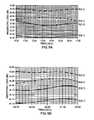
- FIGS. 6A-6Fillustrate the simulated performance for the power combiner/divider of FIG. 5B in terms of S-parameters over a range of frequencies when optimized for two different center frequencies (60 and 73 GHz respectively);
- FIG. 7Aschematically illustrates a perspective view of an exemplary 8-way waveguide portion of a waveguide power combiner/divider in accordance with the present invention
- FIGS. 7B-7Dillustrate the simulated performance at E band for the waveguide power combiner/divider of FIG. 7A in terms of S-parameters, where the eight ports associated with the electromagnetic end launchers are numbered as ports 2-9 and the center coax port is numbered as port 1;
- FIGS. 8A-8Cschematically illustrate perspective and cross-sectional views of an exemplary 8-way waveguide power combiner/divider in accordance with the present invention which incorporates the electromagnetic end launcher of FIGS. 1A-1C into the waveguide portion of FIG. 7A ;
- FIG. 8Dillustrates the simulated performance at V-band for the waveguide power combiner/divider of FIGS. 8A-8C ;
- FIG. 8Eillustrates the simulated effect of ground post position on impedance match S(2,2) in an 8-way waveguide power combiner/divider of the present invention
- FIGS. 9A-9Bschematically illustrate perspective views of exemplary 10-way and N-way waveguide power combiner/dividers in accordance with the present invention, respectively, which incorporate the electromagnetic end launcher of FIGS. 1A-1C ;
- FIGS. 10A-10Bschematically illustrate perspective and side elevation views, respectively, of an exemplary 2-way waveguide portion of a waveguide power combiner/divider in accordance with the present invention, which incorporates two electromagnetic end launchers of FIGS. 1A-1C ;
- FIGS. 11A-11Bschematically illustrate perspective views of an exemplary 16-way waveguide power combiner/divider in accordance with the present invention which incorporates eight 2-way waveguide portions of FIGS. 10A-10B ;
- FIG. 12Aschematically illustrates perspective views of the 16-way waveguide power combiner/divider of FIGS. 11A-11B with a center coax port further coupled to a hollow waveguide;
- FIG. 12Bschematically illustrates a perspective view of two 16-way waveguide power combiner/dividers of FIGS. 11A-11B each having a respective center coax port further coupled to a hollow waveguide;
- FIGS. 13A-13Bschematically illustrate perspective views of an exemplary 8-way waveguide power combiner/divider having an exemplary electromagnetic end launcher in accordance with the present invention in which the transmission line includes a 90 degree turn external to the hollow waveguide;
- FIGS. 14A-14Bschematically illustrate perspective views of an exemplary 16-way waveguide power combiner/divider having an exemplary electromagnetic end launcher similar to that of FIGS. 13A-13B ;
- FIGS. 15A-15Bschematically illustrate perspective views of exemplary solid state power amplifier (SSPA) implementations of waveguide power combiner/dividers in accordance with the present invention
- FIG. 16schematically illustrates a SSPA constructed from a substrate with preamplifiers and a divider network, a waveguide combiner, and MMIC power amplifiers or MMIC power combiner module sub-assemblies, in accordance with the present invention.
- FIG. 17schematically illustrates amplifier circuit block diagrams herein used as amplifier module subassemblies or sub-modules showing that a combiner/divider structure may use cascading 2-way splits to combine/divide 2 or more, e.g., 4 or 8, channels.
- the present inventionprovides waveguide power combiner/dividers which are designed with the recognition that RF power can be more efficiently combined/divided when the power is contained in radiation modes of hollow waveguides rather than in RF signals in transmission lines.
- the term “combiner/divider”is used to refer to a device having a structure which can either combine or divide RF power, depending on how the device is incorporated in an overall system architecture.
- the combiner/dividermay function as a divider if an input signal is provided to the single port and divided output signals delivered to the N ports; conversely, the combiner/divider may function as a combiner if input signals are provided to the N ports and a combined signal is output from the single port.
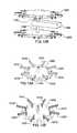
- the present inventionprovides, in one of its aspects, an electromagnetic end launcher 100 for converting RF power to/from RF signals in a transmission line 105 from/to radiation modes of a hollow waveguide 120 , FIG. 1A .
- Exemplary waveguide power combiner/dividers 500 in accordance with the present inventionmay in turn incorporate the electromagnetic end launchers 100 at one or more input/output ports of the waveguide power combiner/divider 500 , FIG. 5A .
- the waveguide power combiner/divider 500may receive four RF transmission line signals, each input at a respective one of the electromagnetic end launchers 100 , which are launched into radiation modes in respective hollow waveguide portions 200 .
- the launched radiation modesmay then combine within the waveguide 250 , and the combined radiation modes may then be converted back into a transmission line mode at a transmission line output port 330 , which may be provided in the form of an air-coax waveguide having a center conductor transmission line 310 and waveguide wall 320 .
- the exemplary electromagnetic end launcher 100 of the present inventionmay include a center conductor transmission line 105 which may be provided in the form of a transmission line waveguide 108 , such as an air-coax waveguide having an outer coaxial waveguide wall 106 with an air dielectric therebetween, for example, FIGS. 1A-1C .
- the electromagnetic end launcher 100may include a launch end 102 in the form of a longitudinally extended portion of the center conductor transmission line 105 which projects into the hollow cavity of a hollow waveguide 120 to provide an end launcher 100 in which the transmission line 105 enters the hollow waveguide 120 parallel to the plane of the hollow waveguide 120 through a waveguide sidewall.
- Alternative configurationsare also possible in which an electromagnetic end launcher 400 , 410 enters a hollow waveguide 420 , 430 perpendicular to the longitudinal axis of the hollow waveguide 420 , 430 either through a side surface or an upper surface of the hollow waveguide 420 , 430 , respectively, FIGS. 4A , 4 B.
- FIG. 4Bthe outer conductor of the coaxial transmission line is not shown protruding above the surface, however it should be clear it would typically follow a similar symmetry as illustrated in FIG. 4A .
- the launch end 102may be supported within the hollow waveguide 120 by a ground post 104 in electrical communication with the center conductor transmission line 105 and a conductive outer wall 122 of the hollow waveguide 120 .
- the ground post 104may have a rectangular or other suitable shape. In exemplary configurations, it may be particularly desirable that the ground post 104 be located longitudinally inward from the distal end 103 of the launch end 102 at a location such that the distal end 103 is suspended to overhang the ground post 104 , i.e., L3>0, FIG. 1C .
- the length L2can be optimized to tune the frequency of operation relative to the height of the ground post 104 (h1) such that the total length (L2+h1) is optimized to be close to a 1 ⁇ 4 of the design wavelength of the RF signals to be combined/divided.
- the dimensions of L2 and h1may be 1.0 mm and 0.52 mm, respectively.
- the waveguide width (w1)may be 3.76 mm for a design at V-band and 3 mm for a design at E-band.
- W1 and L1are also believed to enable structures with a larger bandwidth of operation.
- the height of the waveguide cavity h2, e.g., 1 mmcan also be optimized to further improve the insertion loss of the electromagnetic end launcher 100 .
- simulated performance of reflection coefficient S(1,1) and insertion loss S(2,1)shows acceptable performance of the electromagnetic end launcher 100 at V and E-band, where the transmission line waveguide 108 is numbered as port 1 and the hollow waveguide 120 is numbered has port 2, FIGS. 2A , 2 B.
- reflection at the transmission line waveguide 108is less than 18 dB from 70 GHz to 77 GHz, and the insertion loss from the transmission line waveguide 108 to the hollow waveguide 120 is less than 0.1 dB from 70 GHz to 77 GHz.
- FIGS. 3A , 3 Bsimulate the effect on impedance match as a function of variation in the width of the ground post 104 .
- FIG. 3Csimulates the effect of waveguide height h2 on insertion loss S(2,1).
- the effect of overhang length L3is best illustrated in terms of a complete power combiner/divider structure e.g., combiner/divider 700 , FIG. 7A , and is thus addressed later.
- the simulationsalso demonstrate the need for very good dimensional control and the advantages of a monolithic or nearly monolithic fabrication.
- the structures disclosed herein, such as electromagnetic end launcher 100 , waveguide power combiner/divider 800 , amplifier modules 1614 , or input power divider network 1670 described below,are examples of structures leveraging these advantages.
- FIG. 8the perspective see-through and cross-sectional view in FIGS. 8B , 8 C show the connections between the end-launcher, its electromagnetically shielded feed structure (recta-coaxial in this case), the end launcher 100 itself (a grounded probe structure) at a terminal end, and the waveguide combining structure 750 with waveguides and common combining area.
- the end-launcherits electromagnetically shielded feed structure (recta-coaxial in this case)
- the end launcher 100 itselfa grounded probe structure
- the waveguide combining structure 750with waveguides and common combining area.
- tolerances and mechanical relationships between these elements and their dimensionsthat preferably range from several microns to 10 microns in the EHF range of frequencies.
- the transmission line output port 330may be provided in the form of an air coax waveguide having a center conductor 310 which may be suspended out of contact with the conductive base wall of the waveguide 250 .
- a transmission line output port 350may be provided having a center conductor 353 which is supported by a cylindrical conductive base 352 which is in turn disposed on, and supported by, a base wall of the hollow waveguide 354 .
- the conductive basemay have a thickness of 0.15 mm and diameter of 0.5 mm. The performance of such structures in terms of S-parameters is simulated in FIGS. 6A-6F .
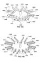
- FIG. 7Aillustrates an 8-way waveguide combiner 700 prior to fitting with electromagnetic end launchers, but including a transmission line output port 730 with center conductor 710 .
- the width of each waveguide portion 750may be about 3 mm, and the height of the waveguide portion 750 may be about 1 mm at V-band or 3.8 mm at E band. Simulated performance of the 8-way waveguide combiner 700 is illustrated in FIGS.
- FIG. 7Billustrates that the transmission line output port 730 is numbered as port 1 and the eight waveguide portions 750 are numbered as ports 2-9 for purposes of defining the S-parameters.
- FIG. 7Billustrates that the reflection loss at the transmission line output port 730 is less than 19 dB from 70 GHz to 77 GHz
- FIG. 7Cillustrates that the insertion loss from the transmission line output port 730 to the waveguide portions 750 is less than 0.1 dB from 70 GHz to 77 GHz
- FIG. 7Dillustrates that the phase from the transmission line output port 732 to the waveguide portions 750 is identical from 70 GHz to 77 GHz.
- the 8-way waveguide combiner 700may form the basis of an 8-way waveguide power combiner/divider 800 , FIG. 8A-8C , in accordance with the present invention with the inclusion, for example, of the electromagnetic end launchers 100 at each waveguide portion 750 to provide eight radial feed points, in a manner similar to that illustrated in FIGS. 1A-1C , 5 A.
- Simulated performance of the 8-way waveguide power combiner/divider 800is illustrated in FIG. 8D , where the transmission line output port 830 is numbered as port 1 and the eight waveguide portions 750 are numbered as ports 2-9 for purposes of defining the S-parameters; the reflection loss at the transmission line output port 830 is less than 20 dB from 70 GHz to 77 GHz.
- the 8-way waveguide power combiner/divider 800also provides a convenient architecture for simulating the effect of overhang length L3.
- higher order exemplary combiner/dividersmay be provided by the present invention, including a 10-way waveguide power combiner/divider 900 up to an N-way waveguide power combiner/divider 950 each of which may include the electromagnetic end launchers 100 of FIGS. 1A-1C , for example.
- Still higher orders of combination/divisionmay be provided by incorporating more than one electromagnetic end launcher 100 in an associated hollow waveguide section 120 .
- two electromagnetic end launchers 1010 , 1020may be provided in a single hollow waveguide section 1030 , FIGS. 10A , 10 B. Similar to the electromagnetic end launcher 100 of FIGS.
- each electromagnetic end launcher 1010 , 1020may include respective ground posts 1014 , 1024 , center conductor transmission lines 1015 , 1025 , and may also include respective longitudinally extended portions 1012 , 1022 of the center conductor transmission lines which project into the hollow cavity of the hollow waveguide 1030 .
- a 16-way waveguide power combiner/divider 1100may then be provided using the double electromagnetic end launchers 1010 , 1020 along with a 8-way waveguide combiner 700 of the type shown in FIG. 7A , for example, FIGS. 11A , 11 B.
- any of the exemplary transmission line output ports 330 , 353 , 730make be configured to further communicate with a hollow output waveguide.
- the transmission line output port 1140 of a waveguide power combiner/divider 1200may include a center conductor transmission line 1142 that has an upwardly extending portion 1143 which may be inserted into the hollow waveguide cavity of an output waveguide 1180 to permit transmission of an RF signal present in the center conductor transmission line 1142 into a radiation mode within the cavity of the hollow output waveguide 1180 .
- two waveguide power combiner/dividers 1200may communicate with a single hollow output waveguide 1280 to transmit respective output signals from a transmission line to radiation modes of the hollow output waveguide 1280 , FIG. 12B .
- combiner/divider or combine/dividedepend on the manner in which the associated device is used.
- the device of FIG. 12Bwould function as a divider.
- waveguide power combiner/dividers 500 , 800 , 900 , 950 , 1100 , 1200have been illustrated with feed through electromagnetic end launchers 100 in-plane and the transmission line output ports 230 , 730 , 1140 perpendicular, other construction axes are possible. For instance, similar performance may be possible when including all inputs and outputs in one plane, all inputs and outputs orthogonal in at least one axis, and other various combinations and variations.
- electromagnetic end launchers 1310 of the present inventionmay enter a waveguide power combiner/divider 1300 , 1400 through an upper wall of the waveguide power combiner/divider 1300 , 1400 , FIGS. 13A-14B .
- a power combiner/divider SSPA 1500 , 1550may include one or more drivers 1512 , pre-drivers 1510 , an N-way input power divider, such as a 4-way divider 1516 or cascading 2-way dividers 1518 - 1520 , amplifier modules 1514 , a microfabricated waveguide power combiner/divider 800 , and/or an air-coax or waveguide output 730 .
- the length of a divider networkmay be the same length in order to keep the same phase.
- N-way combiner/dividersmay be implemented using cascading 2-way splits, which can be done in both waveguides with conducting transmission lines, such as coaxial or hollow core propagating mode waveguide structures, e.g., rectangular and/or folded hollow core waveguides, FIG. 17 .
- the input power dividers 1518 - 1520may use an air-coax line or, a traditional transmission line (e.g. such as a microstrip or stripline), since the input network may not be critical for power combining efficiency.
- the power combiner/divider SSPA 1500 , 1550may include an air-coax combiner, phase shifters, filters and/or linearizers. Signals to be amplified may be fed from an input port 1501 through the circuit into an input divider, for example a Gysel or Wilkinson 2-, 4-, or N-way divider which may be based on waveguides such as micro-coaxial dividers. The divided signal may then be amplified using amplifier modules 1514 with the output power from the amplifier modules 1514 transferred into a microfabricated waveguide power combiner/divider 800 which may incorporate an integrated means of producing a controlled alignment of radiation modes in the waveguide combiner 800 .
- an input dividerfor example a Gysel or Wilkinson 2-, 4-, or N-way divider which may be based on waveguides such as micro-coaxial dividers.
- the divided signalmay then be amplified using amplifier modules 1514 with the output power from the amplifier modules 1514 transferred into a microfabricated waveguide power combiner/divider 800 which may incorporate
- a cooling systeme.g., such as cooling pipes or fins
- a cooling gas or an inert cooling fluidmay be applied within the module, the thermal base plate, or the heat sink.
- a sub-modulemay also be provided which may include multiple MMIC chips that are combined with a low loss air-coax combiner and divider.
- exemplary MMIC chipsmay include a linearization circuit using pre-distortion or feed-forward techniques and/or may use high isolation and low insertion loss switches in sections of the combiner or between stages of the combiner circuit to allow regions to operate relatively independently of other regions without suffering excess inefficiency in the amplifier operating at different power levels.
- Signals from each channelmay then be further combined to higher power levels in a reduced height waveguide combiner and delivered to an air-coax or waveguide output. From a coax output for example, the amplified signal can be transferred to a standard waveguide if a waveguide interface is desired.
- the SSPA 1500 , 1550may be constructed from an upper assembly 1640 and a lower assembly 1650 , SSPA 1600 FIG. 16 .
- the upper assembly 1640may include amplifier modules 1614 , and a microfabricated waveguide power combiner 800 .
- Amplifier modules 1614may be a MMIC such as a power amplifier MMIC, or may be themselves a sub-module or assembly of chips, such as several amplifier MMICs. More than one type of MMIC or chip may be part of the modules 1614 , for example, a phase shifter and/or attenuator may be included before the MMIC power amplifier to adjust phase or power of the power amplifier MMIC or power amplifier transistors.
- the modules or subassemblies 1614may include a divider and combiner network as shown in FIG. 17 , which shows a 4-way and also an 8-way divider and combiner on the input and output ports of the amplifier chips shown in the middle.
- Such an output combiner network for the module 1614may be made, for example, using a micro-coaxial combiner having the advantage of providing port to port isolation.
- the isolationmay be achieved using a combiner structure such as a Wilkinson or Gysel or other suitable transmission line power combiner.
- the lower assembly 1650may include an input power divider network 1670 fabricated using traditional stripline, microstrip, or micro-coax, or a waveguide divider, for example.
- the lower assembly 1650may also include all the direct current (DC) routing (not shown), and the DC lines may be shielded, for example by being separated by ground planes.
- a preamplifiermay be made of one or two stages of amplifier chips or MMICs shown as 1610 and 1612 . They may be integrated into lower assembly 1650 and used to feed or drive the combiner upper assembly 1640 .
- the upper and lower assemblies 1640 , 1650may be configured to be joined to operably interconnect the various components disposed thereon.
- the lower substrate 1650may include recessed areas or openings 1660 , 1662 , 1664 , 1668 to receive the pre-driver 1610 , 1612 , amplifier modules 1614 , and waveguide power combiner/divider 800 , respectively.
- RF signals running through the power divider network 1670may be coupled into the amplifier modules 1614 through respective input ports, as best seen in the assembled SSPAs 1500 , 1550 of FIGS. 15A , 15 B.
- One or more waveguide combinersmay feed one or more waveguide combiners in series and/or parallel. They may combine one or more connector structures to interface to one or more input or output ports. They may be made in a modular format to allow a product that can be scaled upward or downward in power while still using similar components.
- the present inventionrelates to suitable microfabrication processes which permit the precision manufacturing of small parts, typically on a wafer or grid-level or in a batch. For example, processes such as PolyStrata® processing, stereolithography, or solid printing are suitable batch processes where the forming steps act in parallel on a number of parts to provide a sequential build manufacturing process.
- Microfabricationis a manufacturing technology typically whereby the combination of lithographic patterning combined with material additive and/or material removal processes create 3D structures with precision typically in the microns to submicron scale. Often these additive or removal processes are iterative and use one or more of vacuum processing, spin-coating, chemical, plasma, or mechanical processes and are applied across a mostly planar substrate surface in, or on, which the devices will be formed. Step-by-step the iterations typically create the devices on a grid of regions on a surface. The devices are typically formed within, or on top of, substrates including but not limited to silicon, glass, ceramic, and/or metal.
- an 8′′ diameter silicon wafersimilar to those used for making integrated circuits, is often chosen for the wafer's flat surface and the ability for the wafer to survive many additive and/or subtractive material processes with patterning optionally at every layer.
- micro-fabricated structuresare in the square mm size regime.
- the waveguiding components of the waveguide power combiner/dividers and associated componentry illustrated and discussed in connection with FIGS. 1A-17may be monolithically formed together or may be separately formed in one or more parts and then may be integrated using alignment structures formed by the microfabrication process. Since the electromagnetic end launchers together with waveguide power combiner/dividers may be built by a consistent microfabrication process, optimized manufacturing repeatability and/or optimized performance may be achieved at even higher frequencies.
- the PolyStrata® processenables such precision and therefore high quality performance. (The PolyStrata® process is disclosed in U.S. Pat. Nos.
- a key difference between microfabrication methodologies and other related precision machining techniquesis the parallel processing of many devices at a time on at least one substrate (and usually more than one substrate) combined as well as the material complexity and diversity that can be involved.
- a device made of conductors, non-conductors, and containing multiple layers and enclosed regionscannot typically be formed with the precision or complexity using the aforementioned methods without some form of integration, alignment, and bonding.
- most types of precision machiningtypically process only one device at a time as opposed to many devices produced typically in layers in a batch.
- microfabricationWith microfabrication, the additive or subtractive processes are applied across a whole substrate (with sometimes thousands of devices per substrate) at once. Thus, manufacturing of many devices with micron precision can be achieved rapidly with low labor content. Microfabrication has continued to emerge as a leading fabrication approach for future micro-mechanical and micro-electro-mechanical devices.
- the PolyStrata® processcombines the option for processing of both metals and dielectrics in a micromachining technology specifically suited to the manufacture of devices of the present invention.
- the PolyStrata® processmay be used to create air-dielectric microwave transmission components.
- the features of each stratum across a wafermay be defined using photolithography.
- the x-y alignment from layer to layermay be done typically with ⁇ 2 ⁇ m in-plane accuracy, for example, across a 50 mm, 100 mm, 150 mm, 800 mm, or 1200 mm substrate such as a ceramic, SiC, silicon, copper, or stainless steel wafer.
- the wafermay, or may not, contain active devices in or on its surface some of which may be designated to be in communication with the microstructures to be built by the micromachining process.
- active devicesin or on its surface some of which may be designated to be in communication with the microstructures to be built by the micromachining process.
- a photoresist, or molding materialwhich may define the pattern, may be used as a mold for plating conductive features, e.g., a metal, such as copper.
- the coppermay be planarized, for example, using a chemical-mechanical polishing (CMP), lapping, turning, or a combination of these and/or similar methods.
- CMPchemical-mechanical polishing
- the mold material and the fill material such as coppermay or may not be planarized simultaneously in one or more of these steps.
- photo-patternable permanent dielectric supports, features, or sheetsmay be embedded in the device or formed over or in the layer, or the photolithography process begun anew, and the steps repeated. This process may continue until the entire height of the structure or structures being formed has been achieved.
- the photoresist or mold materialmay then be dissolved to leave air-filled copper structures with dielectric supports for the center conductor.
- the resulting structuresmay have strata, or layers, of thicknesses from 5-100 ⁇ m.
- devices and methods of the present inventioncan be expected to provide advances in the art, such as: increased fabrication speed, decreased cost, and increased ease to produce parts in large quantities over traditional machining of parts which require techniques such as EDM or laser processes; increased versatility in producing complex geometries, especially 3D and enclosed geometries; lower loss at high frequencies due to improvements in parasitic effects and substrate tangent loss; increased tolerance control based on monolithic fabrication of electromagnetic end launchers with waveguide power combiner/dividers, affording lower losses at high frequencies such as at Ka-, V-, and W-band, with no need for adjustment or tuning of the positions; increased room for a heat sink, which may improve thermal dissipation; and, reduction of phase and amplitude errors that reduce the combining efficiency.
Landscapes
- Engineering & Computer Science (AREA)
- Power Engineering (AREA)
- Microelectronics & Electronic Packaging (AREA)
- Manufacturing & Machinery (AREA)
- Microwave Amplifiers (AREA)
Abstract
Description
Claims (17)
Priority Applications (2)
| Application Number | Priority Date | Filing Date | Title |
|---|---|---|---|
| US13/726,073US9065163B1 (en) | 2011-12-23 | 2012-12-22 | High frequency power combiner/divider |
| US14/741,775US9490517B2 (en) | 2011-12-23 | 2015-06-17 | High frequency power combiner/divider |
Applications Claiming Priority (2)
| Application Number | Priority Date | Filing Date | Title |
|---|---|---|---|
| US201161580100P | 2011-12-23 | 2011-12-23 | |
| US13/726,073US9065163B1 (en) | 2011-12-23 | 2012-12-22 | High frequency power combiner/divider |
Related Child Applications (1)
| Application Number | Title | Priority Date | Filing Date |
|---|---|---|---|
| US14/741,775ContinuationUS9490517B2 (en) | 2011-12-23 | 2015-06-17 | High frequency power combiner/divider |
Publications (1)
| Publication Number | Publication Date |
|---|---|
| US9065163B1true US9065163B1 (en) | 2015-06-23 |
Family
ID=53397230
Family Applications (2)
| Application Number | Title | Priority Date | Filing Date |
|---|---|---|---|
| US13/726,073Expired - Fee RelatedUS9065163B1 (en) | 2011-12-23 | 2012-12-22 | High frequency power combiner/divider |
| US14/741,775Expired - Fee RelatedUS9490517B2 (en) | 2011-12-23 | 2015-06-17 | High frequency power combiner/divider |
Family Applications After (1)
| Application Number | Title | Priority Date | Filing Date |
|---|---|---|---|
| US14/741,775Expired - Fee RelatedUS9490517B2 (en) | 2011-12-23 | 2015-06-17 | High frequency power combiner/divider |
Country Status (1)
| Country | Link |
|---|---|
| US (2) | US9065163B1 (en) |
Cited By (76)
| Publication number | Priority date | Publication date | Assignee | Title |
|---|---|---|---|---|
| US20140085165A1 (en)* | 2009-05-19 | 2014-03-27 | Marvell World Trade Ltd. | Combining signal power using magnetic coupling between conductors |
| US20150102871A1 (en)* | 2013-10-11 | 2015-04-16 | Teramics LLC | Multiple Way Waveguide Power Module |
| US20150130667A1 (en)* | 2013-09-26 | 2015-05-14 | Pulse Finland Oy | Apparatus and methods for antenna port isolation |
| US20150372378A1 (en)* | 2013-02-07 | 2015-12-24 | Sunnybrook Research Institute | Systems, devices and methods for transmitting electrical signals through a faraday cage |
| US9413052B2 (en) | 2010-07-02 | 2016-08-09 | Nuvotronics, Inc. | Three-dimensional microstructures |
| US9490517B2 (en) | 2011-12-23 | 2016-11-08 | Nuvotronics, Inc. | High frequency power combiner/divider |
| US20160344087A1 (en)* | 2015-05-18 | 2016-11-24 | Cryoelectra Gmbh | Combiner arrangement |
| US9537605B1 (en)* | 2014-07-22 | 2017-01-03 | Bae Systems Information And Electronic Systems Integration Inc. | Ultra-wideband high-power solid-state transmitter for electronic warfare applications |
| US9641144B2 (en) | 2015-06-03 | 2017-05-02 | Space Systems/Loral, Llc | Solid state traveling wave amplifier for space applications |
| US9673503B1 (en)* | 2015-03-30 | 2017-06-06 | David B. Aster | Systems and methods for combining or dividing microwave power |
| US9793593B1 (en) | 2015-03-30 | 2017-10-17 | David B. Aster | Power combiners and dividers including cylindrical conductors and capable of receiving and retaining a gas |
| US9812756B1 (en) | 2015-03-30 | 2017-11-07 | David B. Aster | Systems and methods for combining or dividing microwave power using satellite conductors and capable of receiving and retaining a gas |
| US20170338539A1 (en)* | 2016-05-18 | 2017-11-23 | Continental Microwave and Tool Co., Inc. | N-way, ridged waveguide, radial power combiner/divider |
| CN107658534A (en)* | 2016-07-25 | 2018-02-02 | 克洛依莱克特拉有限公司 | Combiner device |
| US9917355B1 (en) | 2016-10-06 | 2018-03-13 | Toyota Motor Engineering & Manufacturing North America, Inc. | Wide field of view volumetric scan automotive radar with end-fire antenna |
| US9947986B1 (en) | 2015-03-30 | 2018-04-17 | David B. Aster | Reactive power combiners and dividers including nested coaxial conductors |
| US20180108999A1 (en)* | 2016-10-18 | 2018-04-19 | At&T Intellectual Property I, L.P. | Apparatus and methods for launching guided waves via plural waveguide systems |
| US9960469B1 (en) | 2015-03-30 | 2018-05-01 | David B. Aster | Broadband reactive power combiners and dividers including nested coaxial conductors |
| US10020590B2 (en) | 2016-07-19 | 2018-07-10 | Toyota Motor Engineering & Manufacturing North America, Inc. | Grid bracket structure for mm-wave end-fire antenna array |
| US10141636B2 (en) | 2016-09-28 | 2018-11-27 | Toyota Motor Engineering & Manufacturing North America, Inc. | Volumetric scan automotive radar with end-fire antenna on partially laminated multi-layer PCB |
| US10164667B1 (en) | 2018-03-21 | 2018-12-25 | Qorvo Us, Inc. | Spatial power-combining devices with amplifier connectors |
| US10177726B1 (en) | 2016-07-01 | 2019-01-08 | Space Systems/Loral, Llc | Waveguide to microstrip line N-port power splitter/combiner |
| US20190020093A1 (en)* | 2017-07-11 | 2019-01-17 | Commscope Technologies Llc | Method and apparatus for power combining |
| US10193512B1 (en) | 2018-01-05 | 2019-01-29 | Werlatone, Inc. | Phase-shifting power divider/combiner assemblies and systems |
| US10199709B2 (en) | 2016-11-21 | 2019-02-05 | Electronics And Telecommunications Research Institute | Microwave power combiner |
| US20190067781A1 (en) | 2017-08-22 | 2019-02-28 | Qorvo Us, Inc. | Spatial combining device and antenna |
| US20190068141A1 (en) | 2017-08-22 | 2019-02-28 | Qorvo Us, Inc. | Phase tuning for monolithic microwave integrated circuits |
| US20190067782A1 (en)* | 2017-08-22 | 2019-02-28 | Qorvo Us, Inc. | Spatial combining devices for high-frequency operation |
| CN109640507A (en)* | 2017-10-09 | 2019-04-16 | 克洛依莱克特拉有限公司 | High-frequency amplifier unit containing the amplifier module being arranged on outer conductor |
| US10276906B1 (en) | 2015-03-30 | 2019-04-30 | David B. Aster | Systems and methods for combining or dividing microwave power |
| US10312567B2 (en)* | 2016-10-26 | 2019-06-04 | At&T Intellectual Property I, L.P. | Launcher with planar strip antenna and methods for use therewith |
| US20190190111A1 (en)* | 2017-12-20 | 2019-06-20 | Optisys, LLC | Integrated tracking antenna array combiner network |
| US10333209B2 (en) | 2016-07-19 | 2019-06-25 | Toyota Motor Engineering & Manufacturing North America, Inc. | Compact volume scan end-fire radar for vehicle applications |
| US10401491B2 (en) | 2016-11-15 | 2019-09-03 | Toyota Motor Engineering & Manufacturing North America, Inc. | Compact multi range automotive radar assembly with end-fire antennas on both sides of a printed circuit board |
| US10454433B2 (en) | 2017-06-29 | 2019-10-22 | Qorvo Us, Inc. | Amplifier assembly and spatial power combining device |
| US10505253B2 (en)* | 2015-03-16 | 2019-12-10 | Mission Microwave Technologies, Llc | Systems and methods for multi-probe launch power combining |
| US10578689B2 (en) | 2015-12-03 | 2020-03-03 | Innovere Medical Inc. | Systems, devices and methods for wireless transmission of signals through a faraday cage |
| US10585187B2 (en) | 2017-02-24 | 2020-03-10 | Toyota Motor Engineering & Manufacturing North America, Inc. | Automotive radar with end-fire antenna fed by an optically generated signal transmitted through a fiber splitter to enhance a field of view |
| CN110943275A (en)* | 2019-11-27 | 2020-03-31 | 中国船舶重工集团公司第七二四研究所 | Broadband high-power radial waveguide synthesizer and implementation method |
| US10651527B2 (en) | 2017-08-22 | 2020-05-12 | Qorvo Us, Inc. | Spatial power-combining devices with segmented waveguides and antennas |
| US10720711B2 (en) | 2017-08-22 | 2020-07-21 | Qorvo Us, Inc. | Antenna structures for spatial power-combining devices |
| US10741899B2 (en) | 2015-12-22 | 2020-08-11 | Qorvo Us, Inc. | Spatial coupler and antenna for splitting and combining electromagnetic signals |
| US10749276B2 (en) | 2017-08-22 | 2020-08-18 | Qorvo Us, Inc. | Spatial power-combining devices and antenna assemblies |
| US10770775B2 (en)* | 2018-06-08 | 2020-09-08 | SAAB Defense and Security USA LLC t/a Sensor System | Radial combiner |
| US10804588B2 (en) | 2018-12-10 | 2020-10-13 | Qorvo Us, Inc. | Antenna structures for spatial power-combining devices |
| US10812021B2 (en) | 2017-08-22 | 2020-10-20 | Qorvo Us, Inc. | Antenna waveguide transitions for solid state power amplifiers |
| US10833386B2 (en) | 2018-04-09 | 2020-11-10 | Qorvo Us, Inc. | Waveguide transitions for power-combining devices |
| US10855240B2 (en) | 2018-11-15 | 2020-12-01 | Qorvo Us, Inc. | Structures for spatial power-combining devices |
| US10985468B2 (en) | 2019-07-10 | 2021-04-20 | The Boeing Company | Half-patch launcher to provide a signal to a waveguide |
| US11005437B2 (en) | 2019-02-25 | 2021-05-11 | Qorvo Us, Inc. | Spatial power-combining devices with thin film resistors |
| US11081773B2 (en) | 2019-07-10 | 2021-08-03 | The Boeing Company | Apparatus for splitting, amplifying and launching signals into a waveguide to provide a combined transmission signal |
| US11162734B2 (en) | 2018-08-06 | 2021-11-02 | Qorvo Us, Inc. | Heat exchanger assemblies for electronic devices and related methods |
| US11211703B2 (en) | 2019-03-12 | 2021-12-28 | Epirus, Inc. | Systems and methods for dynamic biasing of microwave amplifier |
| US11255608B2 (en) | 2018-08-06 | 2022-02-22 | Qorvo Us, Inc. | Heat exchanger assemblies for electronic devices |
| WO2022087027A1 (en)* | 2020-10-19 | 2022-04-28 | Optisys, LLC | Broadband waveguide to dual-coaxial transition |
| US11374646B2 (en) | 2017-05-09 | 2022-06-28 | Innovere Medical Inc. | Systems and devices for wireless communication through an electromagnetically shielded window |
| US11387791B2 (en) | 2020-03-17 | 2022-07-12 | Qorvo Us, Inc. | Spatial power-combining devices with reduced size |
| US11469722B2 (en) | 2020-06-22 | 2022-10-11 | Epirus, Inc. | Systems and methods for modular power amplifiers |
| US11564337B2 (en) | 2020-03-17 | 2023-01-24 | Qorvo Us, Inc. | Thermal structures for heat transfer devices and spatial power-combining devices |
| US11575749B2 (en)* | 2017-12-30 | 2023-02-07 | Intel Corporation | Low-weight single mm-wave dielectric waveguide interconnect architecture in autonomous cars |
| US11616481B2 (en) | 2020-06-22 | 2023-03-28 | Epirus, Inc. | Systems and methods for modular power amplifiers |
| US11616295B2 (en) | 2019-03-12 | 2023-03-28 | Epirus, Inc. | Systems and methods for adaptive generation of high power electromagnetic radiation and their applications |
| US11621469B2 (en) | 2021-02-01 | 2023-04-04 | Qorvo Us, Inc. | Power-combining devices with increased output power |
| US11658410B2 (en) | 2019-03-12 | 2023-05-23 | Epirus, Inc. | Apparatus and method for synchronizing power circuits with coherent RF signals to form a steered composite RF signal |
| US20230231292A1 (en)* | 2020-06-11 | 2023-07-20 | Thales | Power combiner system comprising four solid-state microwave power amplifiers |
| US11811124B2 (en) | 2020-10-22 | 2023-11-07 | Nokia Technologies Oy | Controllable radio frequency switching and/or splitting device |
| DE102022112314A1 (en) | 2022-05-17 | 2023-11-23 | Muegge Gmbh | Device for combining or dividing microwaves |
| US11949392B1 (en)* | 2021-08-12 | 2024-04-02 | Mission Microwave Technologies, Llc | Broadband power combiner/splitter architecture with low losses |
| US11955687B2 (en) | 2022-01-10 | 2024-04-09 | Qorvo Us, Inc. | Structural arrangements for spatial power-combining devices |
| US12009596B2 (en) | 2021-05-14 | 2024-06-11 | Optisys, Inc. | Planar monolithic combiner and multiplexer for antenna arrays |
| US12068618B2 (en) | 2021-07-01 | 2024-08-20 | Epirus, Inc. | Systems and methods for compact directed energy systems |
| US12160073B1 (en)* | 2022-06-14 | 2024-12-03 | Lockheed Martin Corporation | Symmetric radio frequency coaxial splitters |
| US12183970B2 (en) | 2020-10-29 | 2024-12-31 | Optisys, Inc. | Integrated balancing radiating elements |
| US12272854B1 (en)* | 2022-08-12 | 2025-04-08 | Cobham Advanced Electronic Solutions Inc. | Radial power combiner with cooling loop |
| US12273075B2 (en) | 2021-07-01 | 2025-04-08 | Epirus, Inc. | Systems and methods for power distribution for amplifier arrays |
| US12381523B2 (en) | 2020-06-22 | 2025-08-05 | Epirus, Inc. | Systems and methods for radio frequency power systems |
Families Citing this family (3)
| Publication number | Priority date | Publication date | Assignee | Title |
|---|---|---|---|---|
| CN109768362B (en)* | 2018-12-27 | 2021-04-02 | 西北核技术研究所 | An Octal Microstrip-Rectangular Waveguide Power Combiner |
| RU2725607C1 (en)* | 2019-07-01 | 2020-07-03 | Акционерное общество "Научно-производственное предприятие "Салют" | Microwave power transceiver |
| WO2025135387A1 (en)* | 2023-12-20 | 2025-06-26 | Samsung Electronics Co., Ltd. | Mm-wave signal power divider and antenna array |
Citations (43)
| Publication number | Priority date | Publication date | Assignee | Title |
|---|---|---|---|---|
| US2502479A (en) | 1948-09-24 | 1950-04-04 | Bell Telephone Labor Inc | Semiconductor amplifier |
| US4590446A (en) | 1984-06-28 | 1986-05-20 | Trw Inc. | Radial waveguide power divider/combiner |
| US4812782A (en) | 1985-10-03 | 1989-03-14 | Hughes Aircraft Company | Non-reactive radial line power divider/combiner with integral mode filters |
| US4933651A (en)* | 1988-03-18 | 1990-06-12 | Thomson-Csf | Multichannel combiner/divider |
| US5079527A (en) | 1990-12-06 | 1992-01-07 | Raytheon Company | Recombinant, in-phase, 3-way power divider |
| US5117377A (en) | 1988-10-05 | 1992-05-26 | Finman Paul F | Adaptive control electromagnetic signal analyzer |
| US5126704A (en) | 1991-04-11 | 1992-06-30 | Harris Corporation | Polyphase divider/combiner |
| US5222246A (en) | 1990-11-02 | 1993-06-22 | General Electric Company | Parallel amplifiers with combining phase controlled from combiner difference port |
| US5287069A (en) | 1990-02-07 | 1994-02-15 | Fujitsu Limited | Constant-amplitude wave combination type amplifier |
| US5736898A (en) | 1995-08-04 | 1998-04-07 | Daimler-Benz Aerospace Ag | Process and device for linearizing the gain charactristics and phase-frequency characteristics of traveling-wave tubes and transistor amplifiers at different power levels |
| US5872491A (en) | 1996-11-27 | 1999-02-16 | Kmw Usa, Inc. | Switchable N-way power divider/combiner |
| US5880648A (en) | 1997-04-21 | 1999-03-09 | Myat, Inc. | N-way RF power combiner/divider |
| US5884143A (en) | 1997-02-21 | 1999-03-16 | Lockheed Martin Corporation | Spacecraft with paralleled amplifiers and redundancy |
| US5953811A (en) | 1998-01-20 | 1999-09-21 | Emc Technology Llc | Trimming temperature variable resistor |
| US6046609A (en) | 1996-04-17 | 2000-04-04 | Hitachi, Ltd. | Sense amplifier circuit |
| US6046649A (en) | 1998-11-27 | 2000-04-04 | Lockheed Martin Corporation | Communication system employing paired power amplifiers and drift compensation feedback control loops |
| US6242984B1 (en) | 1998-05-18 | 2001-06-05 | Trw Inc. | Monolithic 3D radial power combiner and splitter |
| US6483397B2 (en) | 2000-11-27 | 2002-11-19 | Raytheon Company | Tandem six port 3:1 divider combiner |
| US6614325B1 (en) | 2000-08-31 | 2003-09-02 | Northrop Grumman Corporation | RF/IF signal distribution network utilizing broadside coupled stripline |
| US20030174018A1 (en) | 2002-03-13 | 2003-09-18 | Cooper Stephen Edward | Circuit comprising amplifiers connected in parallel, and a method of reducing the difference in amplitude between output signals from amplifiers thereof |
| US6753807B1 (en) | 2002-07-30 | 2004-06-22 | The United States Of America As Represented By The Secretary Of Commerce | Combination N-way power divider/combiner and noninvasive reflected power detection |
| US6799020B1 (en) | 1999-07-20 | 2004-09-28 | Qualcomm Incorporated | Parallel amplifier architecture using digital phase control techniques |
| US20050174194A1 (en) | 2004-02-06 | 2005-08-11 | You-Sun Wu | Radial power divider/combiner |
| US7012489B2 (en) | 2003-03-04 | 2006-03-14 | Rohm And Haas Electronic Materials Llc | Coaxial waveguide microstructures and methods of formation thereof |
| US20070001907A1 (en) | 2005-06-29 | 2007-01-04 | Stephen Hall | Method, apparatus, and system for parallel plate mode signaling |
| US7227428B2 (en) | 2002-10-29 | 2007-06-05 | Tdk Corporation | RF module and mode converting structure having magnetic field matching and penetrating conductor patterns |
| US7382212B2 (en) | 2003-01-03 | 2008-06-03 | Thomson Licensing | Transition between a rectangular waveguide and a microstrip line comprised of a single metallized bar |
| US7385462B1 (en) | 2005-03-18 | 2008-06-10 | The United States Of America As Represented By The Administrator Of The National Aeronautics And Space Administration | Wideband radial power combiner/divider fed by a mode transducer |
| US7463109B2 (en) | 2005-04-18 | 2008-12-09 | Furuno Electric Company Ltd. | Apparatus and method for waveguide to microstrip transition having a reduced scale backshort |
| US7482894B2 (en) | 2004-02-06 | 2009-01-27 | L-3 Communications Corporation | Radial power divider/combiner using waveguide impedance transformers |
| US7598805B2 (en) | 2008-01-11 | 2009-10-06 | Freescale Semiconductor, Inc. | Load insensitive balanced power amplifier and related operating method |
| US7616058B1 (en) | 2006-08-28 | 2009-11-10 | Raif Awaida | Radio frequency power combining |
| US7623006B2 (en) | 2006-06-22 | 2009-11-24 | Stmicroelectronics S.A. | Power combiner/splitter |
| US7649432B2 (en) | 2006-12-30 | 2010-01-19 | Nuvotornics, LLC | Three-dimensional microstructures having an embedded and mechanically locked support member and method of formation thereof |
| US7656256B2 (en) | 2006-12-30 | 2010-02-02 | Nuvotronics, PLLC | Three-dimensional microstructures having an embedded support member with an aperture therein and method of formation thereof |
| US7746175B2 (en) | 2006-06-06 | 2010-06-29 | Keragis Corporation | Solid state RF power amplifier |
| US7755174B2 (en) | 2007-03-20 | 2010-07-13 | Nuvotonics, LLC | Integrated electronic components and methods of formation thereof |
| US7898356B2 (en) | 2007-03-20 | 2011-03-01 | Nuvotronics, Llc | Coaxial transmission line microstructures and methods of formation thereof |
| US7932781B2 (en) | 2007-09-12 | 2011-04-26 | Viasat, Inc. | Multi-planar solid state amplifier |
| US20110187453A1 (en) | 2010-01-29 | 2011-08-04 | Wavestream Corporation | Linearizer incorporating a phase shifter |
| WO2012003506A2 (en) | 2010-07-02 | 2012-01-05 | Nuvotronics, Llc | Three-dimensional microstructures |
| US8319583B2 (en) | 2009-08-24 | 2012-11-27 | Raytheon Company | Multi-layer radial power divider/combiner |
| US20130050055A1 (en) | 2011-08-30 | 2013-02-28 | Harris Corporation | Phased array antenna module and method of making same |
Family Cites Families (4)
| Publication number | Priority date | Publication date | Assignee | Title |
|---|---|---|---|---|
| US3023382A (en)* | 1960-07-15 | 1962-02-27 | Microwave Dev Lab Inc | Inline waveguide to coaxial transition |
| US6411174B1 (en)* | 2000-06-14 | 2002-06-25 | Raytheon Company | Compact four-way waveguide power divider |
| US9065163B1 (en) | 2011-12-23 | 2015-06-23 | Nuvotronics, Llc | High frequency power combiner/divider |
| US8952752B1 (en) | 2012-12-12 | 2015-02-10 | Nuvotronics, Llc | Smart power combiner |
- 2012
- 2012-12-22USUS13/726,073patent/US9065163B1/ennot_activeExpired - Fee Related
- 2015
- 2015-06-17USUS14/741,775patent/US9490517B2/ennot_activeExpired - Fee Related
Patent Citations (52)
| Publication number | Priority date | Publication date | Assignee | Title |
|---|---|---|---|---|
| US2502479A (en) | 1948-09-24 | 1950-04-04 | Bell Telephone Labor Inc | Semiconductor amplifier |
| US4590446A (en) | 1984-06-28 | 1986-05-20 | Trw Inc. | Radial waveguide power divider/combiner |
| US4812782A (en) | 1985-10-03 | 1989-03-14 | Hughes Aircraft Company | Non-reactive radial line power divider/combiner with integral mode filters |
| US4933651A (en)* | 1988-03-18 | 1990-06-12 | Thomson-Csf | Multichannel combiner/divider |
| US5117377A (en) | 1988-10-05 | 1992-05-26 | Finman Paul F | Adaptive control electromagnetic signal analyzer |
| US5287069A (en) | 1990-02-07 | 1994-02-15 | Fujitsu Limited | Constant-amplitude wave combination type amplifier |
| US5222246A (en) | 1990-11-02 | 1993-06-22 | General Electric Company | Parallel amplifiers with combining phase controlled from combiner difference port |
| US5079527A (en) | 1990-12-06 | 1992-01-07 | Raytheon Company | Recombinant, in-phase, 3-way power divider |
| US5126704A (en) | 1991-04-11 | 1992-06-30 | Harris Corporation | Polyphase divider/combiner |
| US5736898A (en) | 1995-08-04 | 1998-04-07 | Daimler-Benz Aerospace Ag | Process and device for linearizing the gain charactristics and phase-frequency characteristics of traveling-wave tubes and transistor amplifiers at different power levels |
| US6046609A (en) | 1996-04-17 | 2000-04-04 | Hitachi, Ltd. | Sense amplifier circuit |
| US5872491A (en) | 1996-11-27 | 1999-02-16 | Kmw Usa, Inc. | Switchable N-way power divider/combiner |
| US5884143A (en) | 1997-02-21 | 1999-03-16 | Lockheed Martin Corporation | Spacecraft with paralleled amplifiers and redundancy |
| US5880648A (en) | 1997-04-21 | 1999-03-09 | Myat, Inc. | N-way RF power combiner/divider |
| US5953811A (en) | 1998-01-20 | 1999-09-21 | Emc Technology Llc | Trimming temperature variable resistor |
| US6242984B1 (en) | 1998-05-18 | 2001-06-05 | Trw Inc. | Monolithic 3D radial power combiner and splitter |
| US6046649A (en) | 1998-11-27 | 2000-04-04 | Lockheed Martin Corporation | Communication system employing paired power amplifiers and drift compensation feedback control loops |
| US6799020B1 (en) | 1999-07-20 | 2004-09-28 | Qualcomm Incorporated | Parallel amplifier architecture using digital phase control techniques |
| US6614325B1 (en) | 2000-08-31 | 2003-09-02 | Northrop Grumman Corporation | RF/IF signal distribution network utilizing broadside coupled stripline |
| US6483397B2 (en) | 2000-11-27 | 2002-11-19 | Raytheon Company | Tandem six port 3:1 divider combiner |
| US20030174018A1 (en) | 2002-03-13 | 2003-09-18 | Cooper Stephen Edward | Circuit comprising amplifiers connected in parallel, and a method of reducing the difference in amplitude between output signals from amplifiers thereof |
| US6753807B1 (en) | 2002-07-30 | 2004-06-22 | The United States Of America As Represented By The Secretary Of Commerce | Combination N-way power divider/combiner and noninvasive reflected power detection |
| US7227428B2 (en) | 2002-10-29 | 2007-06-05 | Tdk Corporation | RF module and mode converting structure having magnetic field matching and penetrating conductor patterns |
| US7382212B2 (en) | 2003-01-03 | 2008-06-03 | Thomson Licensing | Transition between a rectangular waveguide and a microstrip line comprised of a single metallized bar |
| US7948335B2 (en) | 2003-03-04 | 2011-05-24 | Nuvotronics, Llc | Coaxial waveguide microstructure having conductive and insulation materials defining voids therein |
| US7405638B2 (en) | 2003-03-04 | 2008-07-29 | Rohm And Haas Electronic Materials Llc | Coaxial waveguide microstructures having an active device and methods of formation thereof |
| US7012489B2 (en) | 2003-03-04 | 2006-03-14 | Rohm And Haas Electronic Materials Llc | Coaxial waveguide microstructures and methods of formation thereof |
| US7148772B2 (en) | 2003-03-04 | 2006-12-12 | Rohm And Haas Electronic Materials Llc | Coaxial waveguide microstructures having an active device and methods of formation thereof |
| US7113056B2 (en) | 2004-02-06 | 2006-09-26 | L-3 Communications Corporation | Radial power divider/combiner |
| US7312673B2 (en) | 2004-02-06 | 2007-12-25 | L-3 Communications Corporation | Radial power divider/combiner |
| US6982613B2 (en) | 2004-02-06 | 2006-01-03 | L-3 Communications Corporation | Radial power divider/combiner |
| US7482894B2 (en) | 2004-02-06 | 2009-01-27 | L-3 Communications Corporation | Radial power divider/combiner using waveguide impedance transformers |
| US20050174194A1 (en) | 2004-02-06 | 2005-08-11 | You-Sun Wu | Radial power divider/combiner |
| US7385462B1 (en) | 2005-03-18 | 2008-06-10 | The United States Of America As Represented By The Administrator Of The National Aeronautics And Space Administration | Wideband radial power combiner/divider fed by a mode transducer |
| US7463109B2 (en) | 2005-04-18 | 2008-12-09 | Furuno Electric Company Ltd. | Apparatus and method for waveguide to microstrip transition having a reduced scale backshort |
| US20070001907A1 (en) | 2005-06-29 | 2007-01-04 | Stephen Hall | Method, apparatus, and system for parallel plate mode signaling |
| US7271680B2 (en) | 2005-06-29 | 2007-09-18 | Intel Corporation | Method, apparatus, and system for parallel plate mode radial pattern signaling |
| US7746175B2 (en) | 2006-06-06 | 2010-06-29 | Keragis Corporation | Solid state RF power amplifier |
| US7623006B2 (en) | 2006-06-22 | 2009-11-24 | Stmicroelectronics S.A. | Power combiner/splitter |
| US7616058B1 (en) | 2006-08-28 | 2009-11-10 | Raif Awaida | Radio frequency power combining |
| US7649432B2 (en) | 2006-12-30 | 2010-01-19 | Nuvotornics, LLC | Three-dimensional microstructures having an embedded and mechanically locked support member and method of formation thereof |
| US7656256B2 (en) | 2006-12-30 | 2010-02-02 | Nuvotronics, PLLC | Three-dimensional microstructures having an embedded support member with an aperture therein and method of formation thereof |
| US8031037B2 (en) | 2006-12-30 | 2011-10-04 | Nuvotronics, Llc | Three-dimensional microstructures and methods of formation thereof |
| US7755174B2 (en) | 2007-03-20 | 2010-07-13 | Nuvotonics, LLC | Integrated electronic components and methods of formation thereof |
| US7898356B2 (en) | 2007-03-20 | 2011-03-01 | Nuvotronics, Llc | Coaxial transmission line microstructures and methods of formation thereof |
| US7932781B2 (en) | 2007-09-12 | 2011-04-26 | Viasat, Inc. | Multi-planar solid state amplifier |
| US7598805B2 (en) | 2008-01-11 | 2009-10-06 | Freescale Semiconductor, Inc. | Load insensitive balanced power amplifier and related operating method |
| US8319583B2 (en) | 2009-08-24 | 2012-11-27 | Raytheon Company | Multi-layer radial power divider/combiner |
| US20110187453A1 (en) | 2010-01-29 | 2011-08-04 | Wavestream Corporation | Linearizer incorporating a phase shifter |
| WO2012003506A2 (en) | 2010-07-02 | 2012-01-05 | Nuvotronics, Llc | Three-dimensional microstructures |
| US20120062335A1 (en) | 2010-07-02 | 2012-03-15 | David Sherrer | Three-dimensional microstructures |
| US20130050055A1 (en) | 2011-08-30 | 2013-02-28 | Harris Corporation | Phased array antenna module and method of making same |
Non-Patent Citations (39)
| Title |
|---|
| Ali Darwish et al.; Three Dimensional Transmission Lines and Power Divider Circuits; 2009 IEEE; pp. 184-190. |
| Ali Darwish et al.; Vertical Balun and Wilkinson Divider; 2002 IEEE MTT-S Digest; pp. 109-112. 2002. |
| AnthonyA. Immorlica, Jr., et al., Miniature 3D Micro-Machined Solid State PowerAmplifiers; Distribution Statement "A" (Approved for Public Release, Distribution Unlimited) N/A. |
| Chance, G.I. et al., "A suspended-membrane balanced frequency doubler at 200GHz," 29th International Conference on Infrared and Millimeter Waves and Terahertz Electronics, pp. 321-322, Karlsrube, 2004. |
| Chen, A.C., "Development of Low-Loss Broad-Band Planar Baluns Using Multilayered Organic Thin Films," IEEE Transactions on Microwave Theory and Techniques, vol. 53, No. 11, pp. 3648-3655, Nov. 2005. |
| Colantonio, P., et al., "High Efficiency RF and Microwave Solid State Power Amplifiers," pp. 380-395, 2009. |
| Comtech EF Data, PCT-4000, 1+1 Phase Combiner Installation and Operation Manual, Revision 2, Oct. 9, 2012. http://www.comtechefdata.com/files/manuals/mn-amplifiers-pdf/mn-pcb4000.pdf Oct. 9, 2012. |
| CPI, Power Amplifer Phase (Power) Combining, Jun. 8, 2005. http://www.ramayes.com/Data%20Files/Communications%20Power%20Industries/CPI%201000-Watt%20Amplifier%20System.pdf. Jun. 8, 2005. |
| Dong, Y., et al., "60 GHz Low Loss, Amplitude and Phase Balanced Radial Waveguide Power Combiner", International Conference on Communications and Control, Sep. 9-11, 2011, pp. 4070-4073. |
| Ehsan, N. et al., "Microcoaxial lines for active hybrid-monolithic circuits," 2009 IEEE MTT-S Int. Microwave.Symp. Boston, MA, Jun. 2009. |
| Ehsan, N., "Broadband Microwave Litographic 3D Components," Dissertation 2009. |
| Extended EP Search Report for EP Application No. 11801527.0 dated Oct. 13, 2014. |
| Filipovic, D. et al., "Monolithic rectangular coaxial lines. Components and systems for commercial and defense applications," Presented at 2008 IASTED Antennas, Radar, and Wave Propagation Conferences, Baltimore, MD, USA, Apr. 2008. |
| Filipovic, D.S., "Design of microfabricated rectangular coaxial lines and components for mm-wave applications," Microwave Review, vol. 12, No. 2, Nov. 2006, pp. 11-16. |
| Guannella, G., "Novel Matching Systems for High Frequencies,": Brown-Boveri Review, vol. 31, Sep. 1944, pp. 327-329. |
| Immorlica, Jr., T. et al., "Miniature 3D micro-machined solid state power amplifiers," COMCAS 2008. |
| Ingram, D.L. et al., "A 427 mW 20% compact W-band InP HEMT MMIC power amplifier," IEEE RFIC Symp. Digest 1999, pp. 95-98. |
| Lukic, M. et al., "Surface-micromachined dual Ka-band cavity backed patch antennas," IEEE Trans. AtennasPropag., vol. 55, pp. 2107-2110, Jul. 2007. |
| Oliver, J.M. et al., "A 3-D micromachined W-band cavity backed patch antenna array with integrated rectacoax transition to wave guide," 2009 Proc. IEEE International Microwave Symposium, Boston, MA 2009. |
| Palacios, T. et al., "High-power AlGaN/GaN HEMTs for Ka-band applications," IEEE Electron Device Letters 26, No. 11 (2005): 781-783. |
| Q Guo et al., A Novel Broadband High-Power Combiner, 2005 IEEE Asia Pacific Microwave Conference Proceedings 2005. |
| Rollin, J.M. et al., "A membrane planar diode for 200GHz mixing applications," 29th International Conference on Infrared and Millimeter Waves and Terahertz Electronics, pp. 205-206, Karlsrube, 2004. |
| Rollin, J.M. et al., "Integrated Schottky diode for a sub-harmonic mixer at millimetre wavelengths," 31st International Conference on Infrared and Millimeter Waves and Terahertz Electronics, Paris, 2006. |
| Saito et al., "Analysis and design of monolithic rectangular coaxial lines for minimum coupling," IEEE Trans. Microwave Theory Tech., vol. 55, pp. 2521-2530, Dec. 2007. |
| Saito, Y., Fontaine, D., Rollin, J-M., Filipovic, D., "Micro-Coaxial Ka-Band Gysel Power Dividers," Microwave Opt Technol Lett 52: 474-478, 2010, Feb. 2010. |
| Sherrer, D, Vanhille, K, Rollin, J.M., "PolyStrata Technology: A Disruptive Approach for 3D Microwave Components and Modules," Presentation (Apr. 23, 2010). |
| Vanhille, K. et al., "Balanced low-loss Ka-band mu-coaxial hybrids," IEEE MTT-S Dig., Honolulu, Hawaii, Jun. 2007. |
| Vanhille, K. et al., "Balanced low-loss Ka-band μ-coaxial hybrids," IEEE MTT-S Dig., Honolulu, Hawaii, Jun. 2007. |
| Vanhille, K. et al., "Ka-Band surface mount directional coupler fabricated using micro-rectangular coaxial transmission lines," 2008 Proc. IEEE International Microwave Symposium, 2008. |
| Vanhille, K., "Design and Characterization of Microfabricated Three-Dimensional Millimeter-Wave Components," Dissertation, 2007. |
| Vanhille, K., et al., "A Capacitively-Loaded Quasi-Planar Ka-Band Resonator" , 36th European Microwave Conference, Sep. 10-15, 2006. |
| Vanhille, K., et al., "Quasi-Planar High-Q Millimeter Wave Resonators", IEEE Transactions on Microwave Theory and Techniques, Jun. 2006. |
| Vanhille, K.J. et al., "Ka-band miniaturized quasi-planar high-Q resonators," IEEE Trans. Microwave Theory Tech., vol. 55, No. 6, pp. 1272-1279, Jun. 2007. |
| Vyas R. et al., "Liquid Crystal Polymer (LCP): The ultimate solution for low-cost RF flexible electronics and antennas," Antennas and Propagation Society, International Symposium, p. 1729-1732 (2007). |
| Wang, H. et al., "Design of a low integrated sub-harmonic mixer at 183GHz using European Schottky diode technology," From Proceedings of the 4th ESA workshop on Millimetre-Wave Technology and Applications, pp. 249-252, Espoo, Finland, Feb. 2006. |
| Wang, H. et al., "Power-amplifier modules covering 70-113 GHz using MMICs," IEEE Trans Microwave Theory and Tech., vol. 39, pp. 9-16, Jan. 2001. |
| Written Opinion of the International Searching Authority mailed Jan. 5, 2012 on PCT/US2011/042902. |
| Written Opinion of the International Searching Authority mailed Jan. 5, 2012 on PCT/US2011/042902. Jan. 5, 2012. |
| York, R.A., et al., "Some considerations for optimal efficiency and low noise is large power combiners," IEEE Transactions on Microwave Theory and Techniques, vol. 49, No. 8, Aug. 2001. |
Cited By (111)
| Publication number | Priority date | Publication date | Assignee | Title |
|---|---|---|---|---|
| US20140085165A1 (en)* | 2009-05-19 | 2014-03-27 | Marvell World Trade Ltd. | Combining signal power using magnetic coupling between conductors |
| US9368857B2 (en)* | 2009-05-19 | 2016-06-14 | Marvell World Trade Ltd. | Combining signal power using magnetic coupling between conductors |
| US9413052B2 (en) | 2010-07-02 | 2016-08-09 | Nuvotronics, Inc. | Three-dimensional microstructures |
| US10305158B2 (en) | 2010-07-02 | 2019-05-28 | Cubic Corporation | Three-dimensional microstructures |
| US9843084B2 (en) | 2010-07-02 | 2017-12-12 | Nuvotronics, Inc | Three-dimensional microstructures |
| US9490517B2 (en) | 2011-12-23 | 2016-11-08 | Nuvotronics, Inc. | High frequency power combiner/divider |
| US20150372378A1 (en)* | 2013-02-07 | 2015-12-24 | Sunnybrook Research Institute | Systems, devices and methods for transmitting electrical signals through a faraday cage |
| US9660336B2 (en)* | 2013-02-07 | 2017-05-23 | Kevan ANDERSON | Systems, devices and methods for transmitting electrical signals through a faraday cage |
| US10090590B2 (en)* | 2013-09-26 | 2018-10-02 | Pulse Finland Oy | Apparatus and methods for antenna port isolation |
| US20150130667A1 (en)* | 2013-09-26 | 2015-05-14 | Pulse Finland Oy | Apparatus and methods for antenna port isolation |
| US20150102871A1 (en)* | 2013-10-11 | 2015-04-16 | Teramics LLC | Multiple Way Waveguide Power Module |
| US9401535B2 (en)* | 2013-10-11 | 2016-07-26 | Teramics LLC | Multiple way waveguide power module |
| US9537605B1 (en)* | 2014-07-22 | 2017-01-03 | Bae Systems Information And Electronic Systems Integration Inc. | Ultra-wideband high-power solid-state transmitter for electronic warfare applications |
| US10505253B2 (en)* | 2015-03-16 | 2019-12-10 | Mission Microwave Technologies, Llc | Systems and methods for multi-probe launch power combining |
| US9673503B1 (en)* | 2015-03-30 | 2017-06-06 | David B. Aster | Systems and methods for combining or dividing microwave power |
| US9812756B1 (en) | 2015-03-30 | 2017-11-07 | David B. Aster | Systems and methods for combining or dividing microwave power using satellite conductors and capable of receiving and retaining a gas |
| US11043725B1 (en) | 2015-03-30 | 2021-06-22 | David B. Aster | Reactive power combiners and dividers including nested coaxial conductors |
| US9793593B1 (en) | 2015-03-30 | 2017-10-17 | David B. Aster | Power combiners and dividers including cylindrical conductors and capable of receiving and retaining a gas |
| US10312565B1 (en) | 2015-03-30 | 2019-06-04 | David B. Aster | Microwave power divider/combiner devices, microwave power divider/combiner bandpass filters, and methods of thermally cooling a cable run |
| US9947986B1 (en) | 2015-03-30 | 2018-04-17 | David B. Aster | Reactive power combiners and dividers including nested coaxial conductors |
| US9793591B1 (en) | 2015-03-30 | 2017-10-17 | David B. Aster | Reactive power dividers/combiners using non-slotted conductors and methods |
| US9960469B1 (en) | 2015-03-30 | 2018-05-01 | David B. Aster | Broadband reactive power combiners and dividers including nested coaxial conductors |
| US10629975B1 (en) | 2015-03-30 | 2020-04-21 | David B. Aster | Systems and methods for combining or dividing microwave power using non-slotted conductors |
| US10276906B1 (en) | 2015-03-30 | 2019-04-30 | David B. Aster | Systems and methods for combining or dividing microwave power |
| US20160344087A1 (en)* | 2015-05-18 | 2016-11-24 | Cryoelectra Gmbh | Combiner arrangement |
| US9641144B2 (en) | 2015-06-03 | 2017-05-02 | Space Systems/Loral, Llc | Solid state traveling wave amplifier for space applications |
| US10578689B2 (en) | 2015-12-03 | 2020-03-03 | Innovere Medical Inc. | Systems, devices and methods for wireless transmission of signals through a faraday cage |
| US10741899B2 (en) | 2015-12-22 | 2020-08-11 | Qorvo Us, Inc. | Spatial coupler and antenna for splitting and combining electromagnetic signals |
| US9979067B2 (en)* | 2016-05-18 | 2018-05-22 | Continental Microwave and Tool Co., Inc. | N-way, ridged waveguide, radial power combiner/divider |
| US20170338539A1 (en)* | 2016-05-18 | 2017-11-23 | Continental Microwave and Tool Co., Inc. | N-way, ridged waveguide, radial power combiner/divider |
| US10177726B1 (en) | 2016-07-01 | 2019-01-08 | Space Systems/Loral, Llc | Waveguide to microstrip line N-port power splitter/combiner |
| US10020590B2 (en) | 2016-07-19 | 2018-07-10 | Toyota Motor Engineering & Manufacturing North America, Inc. | Grid bracket structure for mm-wave end-fire antenna array |
| US10333209B2 (en) | 2016-07-19 | 2019-06-25 | Toyota Motor Engineering & Manufacturing North America, Inc. | Compact volume scan end-fire radar for vehicle applications |
| CN107658534A (en)* | 2016-07-25 | 2018-02-02 | 克洛依莱克特拉有限公司 | Combiner device |
| US10141636B2 (en) | 2016-09-28 | 2018-11-27 | Toyota Motor Engineering & Manufacturing North America, Inc. | Volumetric scan automotive radar with end-fire antenna on partially laminated multi-layer PCB |
| US9917355B1 (en) | 2016-10-06 | 2018-03-13 | Toyota Motor Engineering & Manufacturing North America, Inc. | Wide field of view volumetric scan automotive radar with end-fire antenna |
| US10594040B2 (en) | 2016-10-18 | 2020-03-17 | At&T Intellectual Property I, L.P. | Apparatus and methods for launching guided waves via plural waveguide systems |
| US20180108999A1 (en)* | 2016-10-18 | 2018-04-19 | At&T Intellectual Property I, L.P. | Apparatus and methods for launching guided waves via plural waveguide systems |
| US10340600B2 (en)* | 2016-10-18 | 2019-07-02 | At&T Intellectual Property I, L.P. | Apparatus and methods for launching guided waves via plural waveguide systems |
| US10454178B2 (en) | 2016-10-18 | 2019-10-22 | At&T Intellectual Property I, L.P. | Apparatus and methods for launching guided waves via plural waveguide systems |
| US10312567B2 (en)* | 2016-10-26 | 2019-06-04 | At&T Intellectual Property I, L.P. | Launcher with planar strip antenna and methods for use therewith |
| US10401491B2 (en) | 2016-11-15 | 2019-09-03 | Toyota Motor Engineering & Manufacturing North America, Inc. | Compact multi range automotive radar assembly with end-fire antennas on both sides of a printed circuit board |
| US10199709B2 (en) | 2016-11-21 | 2019-02-05 | Electronics And Telecommunications Research Institute | Microwave power combiner |
| US10585187B2 (en) | 2017-02-24 | 2020-03-10 | Toyota Motor Engineering & Manufacturing North America, Inc. | Automotive radar with end-fire antenna fed by an optically generated signal transmitted through a fiber splitter to enhance a field of view |
| US11374646B2 (en) | 2017-05-09 | 2022-06-28 | Innovere Medical Inc. | Systems and devices for wireless communication through an electromagnetically shielded window |
| US10454433B2 (en) | 2017-06-29 | 2019-10-22 | Qorvo Us, Inc. | Amplifier assembly and spatial power combining device |
| US11024935B2 (en)* | 2017-07-11 | 2021-06-01 | Commscope Technologies Llc | Apparatuses for power combining and power dividing |
| US20190020093A1 (en)* | 2017-07-11 | 2019-01-17 | Commscope Technologies Llc | Method and apparatus for power combining |
| US10615482B2 (en) | 2017-08-22 | 2020-04-07 | Qorvo Us, Inc. | Amplifier assemblies with multiple antenna structures and amplifiers |
| US20190067782A1 (en)* | 2017-08-22 | 2019-02-28 | Qorvo Us, Inc. | Spatial combining devices for high-frequency operation |
| US10587027B2 (en)* | 2017-08-22 | 2020-03-10 | Qorvo Us, Inc. | Spatial combining devices for high-frequency operation |
| US11431294B2 (en) | 2017-08-22 | 2022-08-30 | Qorvo Us, Inc. | Antenna waveguide transitions for solid state power amplifiers |
| US10340574B2 (en) | 2017-08-22 | 2019-07-02 | Qorvo Us, Inc. | Spatial combining device and antenna |
| US20190067781A1 (en) | 2017-08-22 | 2019-02-28 | Qorvo Us, Inc. | Spatial combining device and antenna |
| US10818998B2 (en) | 2017-08-22 | 2020-10-27 | Qorvo Us, Inc. | Spatial power-combining devices with filtering elements |
| US10812021B2 (en) | 2017-08-22 | 2020-10-20 | Qorvo Us, Inc. | Antenna waveguide transitions for solid state power amplifiers |
| US10651527B2 (en) | 2017-08-22 | 2020-05-12 | Qorvo Us, Inc. | Spatial power-combining devices with segmented waveguides and antennas |
| US10707819B2 (en) | 2017-08-22 | 2020-07-07 | Qorvo Us, Inc. | Phase tuning for monolithic microwave integrated circuits |
| US10720711B2 (en) | 2017-08-22 | 2020-07-21 | Qorvo Us, Inc. | Antenna structures for spatial power-combining devices |
| US20190068141A1 (en) | 2017-08-22 | 2019-02-28 | Qorvo Us, Inc. | Phase tuning for monolithic microwave integrated circuits |
| US10749276B2 (en) | 2017-08-22 | 2020-08-18 | Qorvo Us, Inc. | Spatial power-combining devices and antenna assemblies |
| CN109640507A (en)* | 2017-10-09 | 2019-04-16 | 克洛依莱克特拉有限公司 | High-frequency amplifier unit containing the amplifier module being arranged on outer conductor |
| US12381304B2 (en)* | 2017-12-20 | 2025-08-05 | Optisys, Inc. | Integrated tracking antenna array |
| US20190190111A1 (en)* | 2017-12-20 | 2019-06-20 | Optisys, LLC | Integrated tracking antenna array combiner network |
| US11784384B2 (en)* | 2017-12-20 | 2023-10-10 | Optisys, LLC | Integrated tracking antenna array combiner network |
| US20230079336A1 (en)* | 2017-12-20 | 2023-03-16 | Optisys, Inc. | Integrated tracking antenna array |
| US11575749B2 (en)* | 2017-12-30 | 2023-02-07 | Intel Corporation | Low-weight single mm-wave dielectric waveguide interconnect architecture in autonomous cars |
| US10193512B1 (en) | 2018-01-05 | 2019-01-29 | Werlatone, Inc. | Phase-shifting power divider/combiner assemblies and systems |
| US10164667B1 (en) | 2018-03-21 | 2018-12-25 | Qorvo Us, Inc. | Spatial power-combining devices with amplifier connectors |
| US10263651B1 (en) | 2018-03-21 | 2019-04-16 | Qorvo Us, Inc. | Spatial power-combining devices with amplifier connectors |
| US10833386B2 (en) | 2018-04-09 | 2020-11-10 | Qorvo Us, Inc. | Waveguide transitions for power-combining devices |
| US10770775B2 (en)* | 2018-06-08 | 2020-09-08 | SAAB Defense and Security USA LLC t/a Sensor System | Radial combiner |
| US11255608B2 (en) | 2018-08-06 | 2022-02-22 | Qorvo Us, Inc. | Heat exchanger assemblies for electronic devices |
| US11162734B2 (en) | 2018-08-06 | 2021-11-02 | Qorvo Us, Inc. | Heat exchanger assemblies for electronic devices and related methods |
| US10855240B2 (en) | 2018-11-15 | 2020-12-01 | Qorvo Us, Inc. | Structures for spatial power-combining devices |
| US10804588B2 (en) | 2018-12-10 | 2020-10-13 | Qorvo Us, Inc. | Antenna structures for spatial power-combining devices |
| US11005437B2 (en) | 2019-02-25 | 2021-05-11 | Qorvo Us, Inc. | Spatial power-combining devices with thin film resistors |
| US11522286B2 (en) | 2019-03-12 | 2022-12-06 | Epirus, Inc. | Systems and methods for dynamic biasing of microwave amplifier |
| US11658410B2 (en) | 2019-03-12 | 2023-05-23 | Epirus, Inc. | Apparatus and method for synchronizing power circuits with coherent RF signals to form a steered composite RF signal |
| US11211703B2 (en) | 2019-03-12 | 2021-12-28 | Epirus, Inc. | Systems and methods for dynamic biasing of microwave amplifier |
| US12368239B2 (en) | 2019-03-12 | 2025-07-22 | Epirus, Inc. | Systems and methods for dynamic biasing of microwave amplifier |
| US12316017B2 (en) | 2019-03-12 | 2025-05-27 | Epirus, Inc. | Apparatus and method for synchronizing power circuits with coherent RF signals to form a steered composite RF signal |
| US11616295B2 (en) | 2019-03-12 | 2023-03-28 | Epirus, Inc. | Systems and methods for adaptive generation of high power electromagnetic radiation and their applications |
| US11081773B2 (en) | 2019-07-10 | 2021-08-03 | The Boeing Company | Apparatus for splitting, amplifying and launching signals into a waveguide to provide a combined transmission signal |
| US10985468B2 (en) | 2019-07-10 | 2021-04-20 | The Boeing Company | Half-patch launcher to provide a signal to a waveguide |
| CN110943275B (en)* | 2019-11-27 | 2021-08-06 | 中国船舶重工集团公司第七二四研究所 | Broadband high-power radial waveguide synthesizer and implementation method |
| CN110943275A (en)* | 2019-11-27 | 2020-03-31 | 中国船舶重工集团公司第七二四研究所 | Broadband high-power radial waveguide synthesizer and implementation method |
| US11387791B2 (en) | 2020-03-17 | 2022-07-12 | Qorvo Us, Inc. | Spatial power-combining devices with reduced size |
| US11564337B2 (en) | 2020-03-17 | 2023-01-24 | Qorvo Us, Inc. | Thermal structures for heat transfer devices and spatial power-combining devices |
| US11665867B2 (en) | 2020-03-17 | 2023-05-30 | Qorvo Us, Inc. | Thermal structures for heat transfer devices and spatial power-combining devices |
| US12143074B2 (en) | 2020-03-17 | 2024-11-12 | Qorvo Us, Inc. | Spatial power-combining devices with reduced size |
| US20230231292A1 (en)* | 2020-06-11 | 2023-07-20 | Thales | Power combiner system comprising four solid-state microwave power amplifiers |
| US12003223B2 (en) | 2020-06-22 | 2024-06-04 | Epirus, Inc. | Systems and methods for modular power amplifiers |
| US12381523B2 (en) | 2020-06-22 | 2025-08-05 | Epirus, Inc. | Systems and methods for radio frequency power systems |
| US11469722B2 (en) | 2020-06-22 | 2022-10-11 | Epirus, Inc. | Systems and methods for modular power amplifiers |
| US12355408B2 (en) | 2020-06-22 | 2025-07-08 | Epirus, Inc. | Systems and methods for modular power amplifiers |
| US11616481B2 (en) | 2020-06-22 | 2023-03-28 | Epirus, Inc. | Systems and methods for modular power amplifiers |
| WO2022087027A1 (en)* | 2020-10-19 | 2022-04-28 | Optisys, LLC | Broadband waveguide to dual-coaxial transition |
| US12183963B2 (en) | 2020-10-19 | 2024-12-31 | Optisys, Inc. | Device comprising a transition between a waveguide port and two or more coaxial waveguides |
| US11811124B2 (en) | 2020-10-22 | 2023-11-07 | Nokia Technologies Oy | Controllable radio frequency switching and/or splitting device |
| US12183970B2 (en) | 2020-10-29 | 2024-12-31 | Optisys, Inc. | Integrated balancing radiating elements |
| US11621469B2 (en) | 2021-02-01 | 2023-04-04 | Qorvo Us, Inc. | Power-combining devices with increased output power |
| US12009596B2 (en) | 2021-05-14 | 2024-06-11 | Optisys, Inc. | Planar monolithic combiner and multiplexer for antenna arrays |
| US12273075B2 (en) | 2021-07-01 | 2025-04-08 | Epirus, Inc. | Systems and methods for power distribution for amplifier arrays |
| US12068618B2 (en) | 2021-07-01 | 2024-08-20 | Epirus, Inc. | Systems and methods for compact directed energy systems |
| US11949392B1 (en)* | 2021-08-12 | 2024-04-02 | Mission Microwave Technologies, Llc | Broadband power combiner/splitter architecture with low losses |
| US11955687B2 (en) | 2022-01-10 | 2024-04-09 | Qorvo Us, Inc. | Structural arrangements for spatial power-combining devices |
| WO2023222592A1 (en) | 2022-05-17 | 2023-11-23 | Muegge Gmbh | Device for combining or splitting microwaves |
| DE102022112314A1 (en) | 2022-05-17 | 2023-11-23 | Muegge Gmbh | Device for combining or dividing microwaves |
| US12160073B1 (en)* | 2022-06-14 | 2024-12-03 | Lockheed Martin Corporation | Symmetric radio frequency coaxial splitters |
| US12272854B1 (en)* | 2022-08-12 | 2025-04-08 | Cobham Advanced Electronic Solutions Inc. | Radial power combiner with cooling loop |
Also Published As
| Publication number | Publication date |
|---|---|
| US9490517B2 (en) | 2016-11-08 |
| US20160036113A1 (en) | 2016-02-04 |
Similar Documents
| Publication | Publication Date | Title |
|---|---|---|
| US9490517B2 (en) | High frequency power combiner/divider | |
| US11056760B2 (en) | Method of making a low mass foam electrical structure | |
| Tamayo-Domínguez et al. | 3-D-printed modified Butler matrix based on gap waveguide at W-band for monopulse radar | |
| US10305158B2 (en) | Three-dimensional microstructures | |
| JP7278034B2 (en) | Antenna Integrated Printed Wiring Board (“AIPWB”) | |
| US8013784B2 (en) | Butler matrix for 3D integrated RF front-ends | |
| CN102625962B (en) | Precision waveguide interface | |
| US20210005981A1 (en) | Array antenna | |
| EP2783419B1 (en) | High frequency, high bandwidth, low loss microstrip to waveguide transition | |
| US11539107B2 (en) | Substrate integrated waveguide transition including a metallic layer portion having an open portion that is aligned offset from a centerline | |
| JPH11243307A (en) | Millimetric wave ltcc package | |
| US10854984B2 (en) | Air-filled quad-ridge radiator for AESA applications | |
| US12418096B2 (en) | Antenna array architecture with electrically conductive columns between substrates | |
| US11967764B1 (en) | Single antenna with dual circular polarizations and quad feeds for millimeter wave applications | |
| Angeletti et al. | BEAM-FORMING NETWORK DEVELOPMENTS FOR EUROPEAN SATELLITE ANTENNAS. | |
| Menzel et al. | Innovative packaging and fabrication concept for a 28 GHz communication front-end | |
| US12444858B2 (en) | Antenna apparatus employing coplanar waveguide interconnect between RF components | |
| US20240154320A1 (en) | Antenna apparatus employing coplanar waveguide interconnect between rf components | |
| KR102873900B1 (en) | Integrated antenna array having beamformer IC chips with multiple surface interfaces | |
| US20200381837A1 (en) | Waveguide to Stripline Feed |
Legal Events
| Date | Code | Title | Description |
|---|---|---|---|
| AS | Assignment | Owner name:NUVOTRONICS, LLC, VIRGINIA Free format text:ASSIGNMENT OF ASSIGNORS INTEREST;ASSIGNORS:WU, DONALD X.;SHERRER, DAVID W.;ROLLIN, JEAN-MARC;SIGNING DATES FROM 20130109 TO 20130504;REEL/FRAME:030395/0046 | |
| FEPP | Fee payment procedure | Free format text:PAYOR NUMBER ASSIGNED (ORIGINAL EVENT CODE: ASPN); ENTITY STATUS OF PATENT OWNER: LARGE ENTITY | |
| STCF | Information on status: patent grant | Free format text:PATENTED CASE | |
| AS | Assignment | Owner name:NUVOTRONICS, INC., VIRGINIA Free format text:CHANGE OF NAME;ASSIGNOR:NUVOTRONICS, LLC;REEL/FRAME:036851/0027 Effective date:20150630 | |
| MAFP | Maintenance fee payment | Free format text:PAYMENT OF MAINTENANCE FEE, 4TH YEAR, LARGE ENTITY (ORIGINAL EVENT CODE: M1551); ENTITY STATUS OF PATENT OWNER: LARGE ENTITY Year of fee payment:4 | |
| AS | Assignment | Owner name:CUBIC CORPORATION, CALIFORNIA Free format text:ASSIGNMENT OF ASSIGNORS INTEREST;ASSIGNOR:NUVOTRONICS, INC.;REEL/FRAME:048698/0301 Effective date:20190314 | |
| AS | Assignment | Owner name:CUBIC CORPORATION, CALIFORNIA Free format text:CORRECTIVE ASSIGNMENT TO CORRECT THE EFFECTIVE DATE INSIDE THE ASSIGNMENT DOCUMENTATION PREVIOUSLY RECORDED AT REEL: 048698 FRAME: 0301. ASSIGNOR(S) HEREBY CONFIRMS THE ASSIGNMENT;ASSIGNOR:NUVOTRONICS, INC.;REEL/FRAME:048843/0801 Effective date:20190314 | |
| AS | Assignment | Owner name:BARCLAYS BANK PLC, NEW YORK Free format text:FIRST LIEN SECURITY AGREEMENT;ASSIGNORS:CUBIC CORPORATION;PIXIA CORP.;NUVOTRONICS, INC.;REEL/FRAME:056393/0281 Effective date:20210525 Owner name:ALTER DOMUS (US) LLC, ILLINOIS Free format text:SECOND LIEN SECURITY AGREEMENT;ASSIGNORS:CUBIC CORPORATION;PIXIA CORP.;NUVOTRONICS, INC.;REEL/FRAME:056393/0314 Effective date:20210525 | |
| FEPP | Fee payment procedure | Free format text:MAINTENANCE FEE REMINDER MAILED (ORIGINAL EVENT CODE: REM.); ENTITY STATUS OF PATENT OWNER: LARGE ENTITY | |
| LAPS | Lapse for failure to pay maintenance fees | Free format text:PATENT EXPIRED FOR FAILURE TO PAY MAINTENANCE FEES (ORIGINAL EVENT CODE: EXP.); ENTITY STATUS OF PATENT OWNER: LARGE ENTITY | |
| STCH | Information on status: patent discontinuation | Free format text:PATENT EXPIRED DUE TO NONPAYMENT OF MAINTENANCE FEES UNDER 37 CFR 1.362 | |
| FP | Lapsed due to failure to pay maintenance fee | Effective date:20230623 | |
| AS | Assignment | Owner name:CUBIC CORPORATION, CALIFORNIA Free format text:RELEASE OF SECURITY INTEREST AT REEL/FRAME 056393/0281;ASSIGNOR:BARCLAYS BANK PLC, AS ADMINISTRATIVE AGENT;REEL/FRAME:072282/0124 Effective date:20250725 Owner name:CUBIC DEFENSE APPLICATIONS, INC., CALIFORNIA Free format text:RELEASE OF SECURITY INTEREST AT REEL/FRAME 056393/0281;ASSIGNOR:BARCLAYS BANK PLC, AS ADMINISTRATIVE AGENT;REEL/FRAME:072282/0124 Effective date:20250725 Owner name:CUBIC DIGITAL SOLUTIONS LLC (FORMERLY PIXIA CORP.), VIRGINIA Free format text:RELEASE OF SECURITY INTEREST AT REEL/FRAME 056393/0281;ASSIGNOR:BARCLAYS BANK PLC, AS ADMINISTRATIVE AGENT;REEL/FRAME:072282/0124 Effective date:20250725 | |
| AS | Assignment | Owner name:CUBIC CORPORATION, NEW YORK Free format text:RELEASE BY SECURED PARTY;ASSIGNOR:ALTER DOMUS (US) LLC;REEL/FRAME:072281/0176 Effective date:20250725 Owner name:CUBIC DIGITAL SOLUTIONS LLC, NEW YORK Free format text:RELEASE BY SECURED PARTY;ASSIGNOR:ALTER DOMUS (US) LLC;REEL/FRAME:072281/0176 Effective date:20250725 Owner name:NUVOTRONICS, INC., NEW YORK Free format text:RELEASE BY SECURED PARTY;ASSIGNOR:ALTER DOMUS (US) LLC;REEL/FRAME:072281/0176 Effective date:20250725 |