US9064866B2 - High-k dielectrics with gold nano-particles - Google Patents
High-k dielectrics with gold nano-particlesDownload PDFInfo
- Publication number
- US9064866B2 US9064866B2US13/757,290US201313757290AUS9064866B2US 9064866 B2US9064866 B2US 9064866B2US 201313757290 AUS201313757290 AUS 201313757290AUS 9064866 B2US9064866 B2US 9064866B2
- Authority
- US
- United States
- Prior art keywords
- layer
- dielectric
- thickness
- oxide
- substrate
- Prior art date
- Legal status (The legal status is an assumption and is not a legal conclusion. Google has not performed a legal analysis and makes no representation as to the accuracy of the status listed.)
- Active, expires
Links
- 239000010931goldSubstances0.000titleclaimsabstractdescription28
- PCHJSUWPFVWCPO-UHFFFAOYSA-NgoldChemical compound[Au]PCHJSUWPFVWCPO-UHFFFAOYSA-N0.000titleclaimsabstractdescription26
- 229910052737goldInorganic materials0.000titleclaimsabstractdescription24
- 239000002105nanoparticleSubstances0.000titleclaimsabstractdescription24
- 239000003989dielectric materialSubstances0.000titledescription18
- 239000012212insulatorSubstances0.000claimsabstractdescription39
- 229910052751metalInorganic materials0.000claimsabstractdescription32
- 239000002184metalSubstances0.000claimsabstractdescription32
- 229910044991metal oxideInorganic materials0.000claimsabstractdescription20
- 150000004706metal oxidesChemical class0.000claimsabstractdescription16
- VYPSYNLAJGMNEJ-UHFFFAOYSA-NSilicium dioxideChemical compoundO=[Si]=OVYPSYNLAJGMNEJ-UHFFFAOYSA-N0.000claimsdescription140
- 239000000463materialSubstances0.000claimsdescription112
- 239000000758substrateSubstances0.000claimsdescription71
- 239000000377silicon dioxideSubstances0.000claimsdescription63
- XUIMIQQOPSSXEZ-UHFFFAOYSA-NSiliconChemical compound[Si]XUIMIQQOPSSXEZ-UHFFFAOYSA-N0.000claimsdescription31
- 229910052710siliconInorganic materials0.000claimsdescription31
- 239000010703siliconSubstances0.000claimsdescription31
- 229910000449hafnium oxideInorganic materials0.000claimsdescription28
- 230000015654memoryEffects0.000claimsdescription24
- WIHZLLGSGQNAGK-UHFFFAOYSA-Nhafnium(4+);oxygen(2-)Chemical compound[O-2].[O-2].[Hf+4]WIHZLLGSGQNAGK-UHFFFAOYSA-N0.000claimsdescription22
- 235000012239silicon dioxideNutrition0.000claimsdescription20
- 239000004020conductorSubstances0.000claimsdescription8
- VBJZVLUMGGDVMO-UHFFFAOYSA-Nhafnium atomChemical compound[Hf]VBJZVLUMGGDVMO-UHFFFAOYSA-N0.000claimsdescription8
- 239000002245particleSubstances0.000claimsdescription7
- 238000009792diffusion processMethods0.000claimsdescription6
- BASFCYQUMIYNBI-UHFFFAOYSA-NplatinumChemical compound[Pt]BASFCYQUMIYNBI-UHFFFAOYSA-N0.000claimsdescription6
- GWEVSGVZZGPLCZ-UHFFFAOYSA-NTitan oxideChemical compoundO=[Ti]=OGWEVSGVZZGPLCZ-UHFFFAOYSA-N0.000claimsdescription4
- 229910052732germaniumInorganic materials0.000claimsdescription4
- GNPVGFCGXDBREM-UHFFFAOYSA-Ngermanium atomChemical compound[Ge]GNPVGFCGXDBREM-UHFFFAOYSA-N0.000claimsdescription4
- 230000003746surface roughnessEffects0.000claimsdescription4
- 238000011109contaminationMethods0.000claimsdescription3
- 229910052697platinumInorganic materials0.000claimsdescription3
- JBRZTFJDHDCESZ-UHFFFAOYSA-NAsGaChemical compound[As]#[Ga]JBRZTFJDHDCESZ-UHFFFAOYSA-N0.000claimsdescription2
- 229910001218Gallium arsenideInorganic materials0.000claimsdescription2
- NRTOMJZYCJJWKI-UHFFFAOYSA-NTitanium nitrideChemical compound[Ti]#NNRTOMJZYCJJWKI-UHFFFAOYSA-N0.000claimsdescription2
- RVTZCBVAJQQJTK-UHFFFAOYSA-Noxygen(2-);zirconium(4+)Chemical compound[O-2].[O-2].[Zr+4]RVTZCBVAJQQJTK-UHFFFAOYSA-N0.000claimsdescription2
- 229910052594sapphireInorganic materials0.000claimsdescription2
- 239000010980sapphireSubstances0.000claimsdescription2
- OGIDPMRJRNCKJF-UHFFFAOYSA-Ntitanium oxideInorganic materials[Ti]=OOGIDPMRJRNCKJF-UHFFFAOYSA-N0.000claimsdescription2
- MAKDTFFYCIMFQP-UHFFFAOYSA-Ntitanium tungstenChemical compound[Ti].[W]MAKDTFFYCIMFQP-UHFFFAOYSA-N0.000claimsdescription2
- 229910001928zirconium oxideInorganic materials0.000claimsdescription2
- 238000000231atomic layer depositionMethods0.000abstractdescription65
- 238000000034methodMethods0.000abstractdescription36
- 239000004065semiconductorSubstances0.000abstractdescription31
- 239000003990capacitorSubstances0.000abstractdescription8
- 238000012876topographyMethods0.000abstractdescription2
- 230000002085persistent effectEffects0.000abstract1
- 230000005641tunnelingEffects0.000abstract1
- 239000010410layerSubstances0.000description223
- 239000002243precursorSubstances0.000description84
- 239000007789gasSubstances0.000description52
- 238000006243chemical reactionMethods0.000description38
- 238000010926purgeMethods0.000description37
- 239000010408filmSubstances0.000description35
- 239000000376reactantSubstances0.000description33
- 238000000151depositionMethods0.000description30
- 230000008021depositionEffects0.000description27
- 230000008569processEffects0.000description17
- 229910052814silicon oxideInorganic materials0.000description17
- 230000006870functionEffects0.000description15
- 238000007667floatingMethods0.000description12
- 238000004519manufacturing processMethods0.000description12
- XLYOFNOQVPJJNP-UHFFFAOYSA-NwaterSubstancesOXLYOFNOQVPJJNP-UHFFFAOYSA-N0.000description11
- 239000007787solidSubstances0.000description10
- 230000015572biosynthetic processEffects0.000description9
- 239000006227byproductSubstances0.000description9
- 238000001704evaporationMethods0.000description9
- 230000002829reductive effectEffects0.000description9
- 239000002356single layerSubstances0.000description9
- IJGRMHOSHXDMSA-UHFFFAOYSA-NAtomic nitrogenChemical compoundN#NIJGRMHOSHXDMSA-UHFFFAOYSA-N0.000description8
- 238000005229chemical vapour depositionMethods0.000description8
- 230000008020evaporationEffects0.000description8
- 235000012431wafersNutrition0.000description8
- MHAJPDPJQMAIIY-UHFFFAOYSA-NHydrogen peroxideChemical compoundOOMHAJPDPJQMAIIY-UHFFFAOYSA-N0.000description7
- -1SnO2Chemical class0.000description7
- 230000004888barrier functionEffects0.000description7
- 230000007547defectEffects0.000description7
- 238000010586diagramMethods0.000description7
- XKRFYHLGVUSROY-UHFFFAOYSA-NArgonChemical compound[Ar]XKRFYHLGVUSROY-UHFFFAOYSA-N0.000description6
- PDPJQWYGJJBYLF-UHFFFAOYSA-Jhafnium tetrachlorideChemical compoundCl[Hf](Cl)(Cl)ClPDPJQWYGJJBYLF-UHFFFAOYSA-J0.000description6
- 238000004544sputter depositionMethods0.000description6
- QVGXLLKOCUKJST-UHFFFAOYSA-Natomic oxygenChemical compound[O]QVGXLLKOCUKJST-UHFFFAOYSA-N0.000description5
- 230000008901benefitEffects0.000description5
- 230000001276controlling effectEffects0.000description5
- 230000007423decreaseEffects0.000description5
- 230000000694effectsEffects0.000description5
- 230000005684electric fieldEffects0.000description5
- 229910052735hafniumInorganic materials0.000description5
- 230000001590oxidative effectEffects0.000description5
- 239000001301oxygenSubstances0.000description5
- 229910052760oxygenInorganic materials0.000description5
- 229910021420polycrystalline siliconInorganic materials0.000description5
- 229920005591polysiliconPolymers0.000description5
- 239000000126substanceSubstances0.000description5
- GQPLMRYTRLFLPF-UHFFFAOYSA-NNitrous OxideChemical compound[O-][N+]#NGQPLMRYTRLFLPF-UHFFFAOYSA-N0.000description4
- CBENFWSGALASAD-UHFFFAOYSA-NOzoneChemical compound[O-][O+]=OCBENFWSGALASAD-UHFFFAOYSA-N0.000description4
- MCMNRKCIXSYSNV-UHFFFAOYSA-NZirconium dioxideChemical compoundO=[Zr]=OMCMNRKCIXSYSNV-UHFFFAOYSA-N0.000description4
- 229910045601alloyInorganic materials0.000description4
- 239000000956alloySubstances0.000description4
- PNEYBMLMFCGWSK-UHFFFAOYSA-Naluminium oxideInorganic materials[O-2].[O-2].[O-2].[Al+3].[Al+3]PNEYBMLMFCGWSK-UHFFFAOYSA-N0.000description4
- 150000002739metalsChemical class0.000description4
- 229910052757nitrogenInorganic materials0.000description4
- 230000003647oxidationEffects0.000description4
- 238000007254oxidation reactionMethods0.000description4
- 238000012545processingMethods0.000description4
- 239000000047productSubstances0.000description4
- 229910001868waterInorganic materials0.000description4
- 229910052786argonInorganic materials0.000description3
- 125000004429atomChemical group0.000description3
- 210000004027cellAnatomy0.000description3
- 229910052593corundumInorganic materials0.000description3
- 230000008878couplingEffects0.000description3
- 238000010168coupling processMethods0.000description3
- 238000005859coupling reactionMethods0.000description3
- 238000009826distributionMethods0.000description3
- 238000010438heat treatmentMethods0.000description3
- 239000001257hydrogenSubstances0.000description3
- 229910052739hydrogenInorganic materials0.000description3
- 125000004435hydrogen atomChemical class[H]*0.000description3
- 239000011261inert gasSubstances0.000description3
- 238000002955isolationMethods0.000description3
- 230000000670limiting effectEffects0.000description3
- 239000007788liquidSubstances0.000description3
- 239000000203mixtureSubstances0.000description3
- 229910052754neonInorganic materials0.000description3
- GKAOGPIIYCISHV-UHFFFAOYSA-Nneon atomChemical compound[Ne]GKAOGPIIYCISHV-UHFFFAOYSA-N0.000description3
- MWUXSHHQAYIFBG-UHFFFAOYSA-Nnitrogen oxideInorganic materialsO=[N]MWUXSHHQAYIFBG-UHFFFAOYSA-N0.000description3
- 230000002093peripheral effectEffects0.000description3
- 230000001360synchronised effectEffects0.000description3
- 239000010936titaniumSubstances0.000description3
- 229910001845yogo sapphireInorganic materials0.000description3
- MYMOFIZGZYHOMD-UHFFFAOYSA-NDioxygenChemical compoundO=OMYMOFIZGZYHOMD-UHFFFAOYSA-N0.000description2
- KRHYYFGTRYWZRS-UHFFFAOYSA-NFluoraneChemical compoundFKRHYYFGTRYWZRS-UHFFFAOYSA-N0.000description2
- 229910002651NO3Inorganic materials0.000description2
- BLRPTPMANUNPDV-UHFFFAOYSA-NSilaneChemical compound[SiH4]BLRPTPMANUNPDV-UHFFFAOYSA-N0.000description2
- RTAQQCXQSZGOHL-UHFFFAOYSA-NTitaniumChemical compound[Ti]RTAQQCXQSZGOHL-UHFFFAOYSA-N0.000description2
- 229910052782aluminiumInorganic materials0.000description2
- XAGFODPZIPBFFR-UHFFFAOYSA-NaluminiumChemical compound[Al]XAGFODPZIPBFFR-UHFFFAOYSA-N0.000description2
- 238000003877atomic layer epitaxyMethods0.000description2
- 230000000903blocking effectEffects0.000description2
- 210000000746body regionAnatomy0.000description2
- 239000000969carrierSubstances0.000description2
- 239000002800charge carrierSubstances0.000description2
- 239000007795chemical reaction productSubstances0.000description2
- 238000004140cleaningMethods0.000description2
- 239000002131composite materialSubstances0.000description2
- 238000002425crystallisationMethods0.000description2
- 230000008025crystallizationEffects0.000description2
- 238000000354decomposition reactionMethods0.000description2
- 238000005137deposition processMethods0.000description2
- 229910001882dioxygenInorganic materials0.000description2
- 238000005516engineering processMethods0.000description2
- 230000005669field effectEffects0.000description2
- 229910001922gold oxideInorganic materials0.000description2
- YCJQNNVSZNFWAH-UHFFFAOYSA-Jhafnium(4+);tetraiodideChemical compoundI[Hf](I)(I)IYCJQNNVSZNFWAH-UHFFFAOYSA-J0.000description2
- CJNBYAVZURUTKZ-UHFFFAOYSA-Nhafnium(iv) oxideChemical compoundO=[Hf]=OCJNBYAVZURUTKZ-UHFFFAOYSA-N0.000description2
- 239000012705liquid precursorSubstances0.000description2
- 230000007774longtermEffects0.000description2
- 230000007246mechanismEffects0.000description2
- 238000004377microelectronicMethods0.000description2
- 238000002360preparation methodMethods0.000description2
- 238000012163sequencing techniqueMethods0.000description2
- 229910000077silaneInorganic materials0.000description2
- LIVNPJMFVYWSIS-UHFFFAOYSA-Nsilicon monoxideChemical class[Si-]#[O+]LIVNPJMFVYWSIS-UHFFFAOYSA-N0.000description2
- 238000003860storageMethods0.000description2
- 239000010409thin filmSubstances0.000description2
- XOLBLPGZBRYERU-UHFFFAOYSA-Ntin dioxideChemical compoundO=[Sn]=OXOLBLPGZBRYERU-UHFFFAOYSA-N0.000description2
- 229910052719titaniumInorganic materials0.000description2
- 230000007704transitionEffects0.000description2
- WFKWXMTUELFFGS-UHFFFAOYSA-NtungstenChemical compound[W]WFKWXMTUELFFGS-UHFFFAOYSA-N0.000description2
- 239000010937tungstenSubstances0.000description2
- 229910052721tungstenInorganic materials0.000description2
- 229910003099(Y2O3)x(ZrO2)1−xInorganic materials0.000description1
- MGWGWNFMUOTEHG-UHFFFAOYSA-N4-(3,5-dimethylphenyl)-1,3-thiazol-2-amineChemical compoundCC1=CC(C)=CC(C=2N=C(N)SC=2)=C1MGWGWNFMUOTEHG-UHFFFAOYSA-N0.000description1
- VXEGSRKPIUDPQT-UHFFFAOYSA-N4-[4-(4-methoxyphenyl)piperazin-1-yl]anilineChemical compoundC1=CC(OC)=CC=C1N1CCN(C=2C=CC(N)=CC=2)CC1VXEGSRKPIUDPQT-UHFFFAOYSA-N0.000description1
- OKTJSMMVPCPJKN-UHFFFAOYSA-NCarbonChemical compound[C]OKTJSMMVPCPJKN-UHFFFAOYSA-N0.000description1
- 229910002244LaAlO3Inorganic materials0.000description1
- 229910052581Si3N4Inorganic materials0.000description1
- 229910004298SiO 2Inorganic materials0.000description1
- 239000005083Zinc sulfideSubstances0.000description1
- QCWXUUIWCKQGHC-UHFFFAOYSA-NZirconiumChemical compound[Zr]QCWXUUIWCKQGHC-UHFFFAOYSA-N0.000description1
- 238000010521absorption reactionMethods0.000description1
- 239000002253acidSubstances0.000description1
- 230000006978adaptationEffects0.000description1
- 239000002099adlayerSubstances0.000description1
- 150000001298alcoholsChemical class0.000description1
- 229910052784alkaline earth metalInorganic materials0.000description1
- 229910002065alloy metalInorganic materials0.000description1
- 229910021486amorphous silicon dioxideInorganic materials0.000description1
- 238000000137annealingMethods0.000description1
- 229910002056binary alloyInorganic materials0.000description1
- 230000005540biological transmissionEffects0.000description1
- 229910052799carbonInorganic materials0.000description1
- 230000015556catabolic processEffects0.000description1
- CETPSERCERDGAM-UHFFFAOYSA-Nceric oxideChemical compoundO=[Ce]=OCETPSERCERDGAM-UHFFFAOYSA-N0.000description1
- 229910000421cerium(III) oxideInorganic materials0.000description1
- 229910000422cerium(IV) oxideInorganic materials0.000description1
- 230000008859changeEffects0.000description1
- 238000004891communicationMethods0.000description1
- 230000000295complement effectEffects0.000description1
- 238000009833condensationMethods0.000description1
- 230000005494condensationEffects0.000description1
- 238000010276constructionMethods0.000description1
- 239000000356contaminantSubstances0.000description1
- 239000013078crystalSubstances0.000description1
- 230000003247decreasing effectEffects0.000description1
- 230000002950deficientEffects0.000description1
- 230000001419dependent effectEffects0.000description1
- 238000001514detection methodMethods0.000description1
- MROCJMGDEKINLD-UHFFFAOYSA-NdichlorosilaneChemical compoundCl[SiH2]ClMROCJMGDEKINLD-UHFFFAOYSA-N0.000description1
- NLQFUUYNQFMIJW-UHFFFAOYSA-Ndysprosium(III) oxideInorganic materialsO=[Dy]O[Dy]=ONLQFUUYNQFMIJW-UHFFFAOYSA-N0.000description1
- VQCBHWLJZDBHOS-UHFFFAOYSA-Nerbium(III) oxideInorganic materialsO=[Er]O[Er]=OVQCBHWLJZDBHOS-UHFFFAOYSA-N0.000description1
- 238000005530etchingMethods0.000description1
- RSEIMSPAXMNYFJ-UHFFFAOYSA-Neuropium(III) oxideInorganic materialsO=[Eu]O[Eu]=ORSEIMSPAXMNYFJ-UHFFFAOYSA-N0.000description1
- 239000000835fiberSubstances0.000description1
- CMIHHWBVHJVIGI-UHFFFAOYSA-Ngadolinium(III) oxideInorganic materials[O-2].[O-2].[O-2].[Gd+3].[Gd+3]CMIHHWBVHJVIGI-UHFFFAOYSA-N0.000description1
- 238000007429general methodMethods0.000description1
- TZNXTUDMYCRCAP-UHFFFAOYSA-Nhafnium(4+);tetranitrateChemical compound[Hf+4].[O-][N+]([O-])=O.[O-][N+]([O-])=O.[O-][N+]([O-])=O.[O-][N+]([O-])=OTZNXTUDMYCRCAP-UHFFFAOYSA-N0.000description1
- 229910052736halogenInorganic materials0.000description1
- 150000002367halogensChemical class0.000description1
- 239000001307heliumSubstances0.000description1
- 229910052734heliumInorganic materials0.000description1
- SWQJXJOGLNCZEY-UHFFFAOYSA-Nhelium atomChemical compound[He]SWQJXJOGLNCZEY-UHFFFAOYSA-N0.000description1
- 238000009413insulationMethods0.000description1
- 230000003993interactionEffects0.000description1
- 229910052743kryptonInorganic materials0.000description1
- DNNSSWSSYDEUBZ-UHFFFAOYSA-Nkrypton atomChemical compound[Kr]DNNSSWSSYDEUBZ-UHFFFAOYSA-N0.000description1
- 239000005001laminate filmSubstances0.000description1
- 229910000311lanthanide oxideInorganic materials0.000description1
- 229910052747lanthanoidInorganic materials0.000description1
- MRELNEQAGSRDBK-UHFFFAOYSA-Nlanthanum oxideInorganic materials[O-2].[O-2].[O-2].[La+3].[La+3]MRELNEQAGSRDBK-UHFFFAOYSA-N0.000description1
- 239000011344liquid materialSubstances0.000description1
- 229910003443lutetium oxideInorganic materials0.000description1
- 238000005259measurementMethods0.000description1
- 150000001247metal acetylidesChemical class0.000description1
- 239000002082metal nanoparticleSubstances0.000description1
- 238000001465metallisationMethods0.000description1
- 230000004048modificationEffects0.000description1
- 238000012986modificationMethods0.000description1
- PLDDOISOJJCEMH-UHFFFAOYSA-Nneodymium oxideInorganic materials[O-2].[O-2].[O-2].[Nd+3].[Nd+3]PLDDOISOJJCEMH-UHFFFAOYSA-N0.000description1
- 150000004767nitridesChemical class0.000description1
- JCXJVPUVTGWSNB-UHFFFAOYSA-Nnitrogen dioxideInorganic materialsO=[N]=OJCXJVPUVTGWSNB-UHFFFAOYSA-N0.000description1
- 239000001272nitrous oxideSubstances0.000description1
- 239000000615nonconductorSubstances0.000description1
- 150000002894organic compoundsChemical class0.000description1
- KTUFCUMIWABKDW-UHFFFAOYSA-Noxo(oxolanthaniooxy)lanthanumChemical compoundO=[La]O[La]=OKTUFCUMIWABKDW-UHFFFAOYSA-N0.000description1
- 230000036961partial effectEffects0.000description1
- 238000005289physical depositionMethods0.000description1
- 238000005240physical vapour depositionMethods0.000description1
- 210000002381plasmaAnatomy0.000description1
- 229910021426porous siliconInorganic materials0.000description1
- 239000000843powderSubstances0.000description1
- 238000005086pumpingMethods0.000description1
- 239000012713reactive precursorSubstances0.000description1
- 230000009467reductionEffects0.000description1
- 239000003870refractory metalSubstances0.000description1
- 230000001105regulatory effectEffects0.000description1
- FKTOIHSPIPYAPE-UHFFFAOYSA-Nsamarium(III) oxideInorganic materials[O-2].[O-2].[O-2].[Sm+3].[Sm+3]FKTOIHSPIPYAPE-UHFFFAOYSA-N0.000description1
- VSZWPYCFIRKVQL-UHFFFAOYSA-Nselanylidenegallium;seleniumChemical compound[Se].[Se]=[Ga].[Se]=[Ga]VSZWPYCFIRKVQL-UHFFFAOYSA-N0.000description1
- 229910021332silicideInorganic materials0.000description1
- 239000005049silicon tetrachlorideSubstances0.000description1
- 239000011343solid materialSubstances0.000description1
- 238000001179sorption measurementMethods0.000description1
- 230000003068static effectEffects0.000description1
- 238000000859sublimationMethods0.000description1
- 230000008022sublimationEffects0.000description1
- 238000005382thermal cyclingMethods0.000description1
- ZIKATJAYWZUJPY-UHFFFAOYSA-Nthulium (III) oxideInorganic materials[O-2].[O-2].[O-2].[Tm+3].[Tm+3]ZIKATJAYWZUJPY-UHFFFAOYSA-N0.000description1
- 230000036962time dependentEffects0.000description1
- 229910001887tin oxideInorganic materials0.000description1
- QHGNHLZPVBIIPX-UHFFFAOYSA-Ntin(ii) oxideChemical class[Sn]=OQHGNHLZPVBIIPX-UHFFFAOYSA-N0.000description1
- 238000012546transferMethods0.000description1
- FIXNOXLJNSSSLJ-UHFFFAOYSA-Nytterbium(III) oxideInorganic materialsO=[Yb]O[Yb]=OFIXNOXLJNSSSLJ-UHFFFAOYSA-N0.000description1
- 229910052984zinc sulfideInorganic materials0.000description1
- DRDVZXDWVBGGMH-UHFFFAOYSA-Nzinc;sulfideChemical compound[S-2].[Zn+2]DRDVZXDWVBGGMH-UHFFFAOYSA-N0.000description1
- 229910052726zirconiumInorganic materials0.000description1
Images


Classifications
- H01L29/517—
- H—ELECTRICITY
- H10—SEMICONDUCTOR DEVICES; ELECTRIC SOLID-STATE DEVICES NOT OTHERWISE PROVIDED FOR
- H10D—INORGANIC ELECTRIC SEMICONDUCTOR DEVICES
- H10D64/00—Electrodes of devices having potential barriers
- H10D64/60—Electrodes characterised by their materials
- H10D64/66—Electrodes having a conductor capacitively coupled to a semiconductor by an insulator, e.g. MIS electrodes
- H10D64/68—Electrodes having a conductor capacitively coupled to a semiconductor by an insulator, e.g. MIS electrodes characterised by the insulator, e.g. by the gate insulator
- H10D64/691—Electrodes having a conductor capacitively coupled to a semiconductor by an insulator, e.g. MIS electrodes characterised by the insulator, e.g. by the gate insulator comprising metallic compounds, e.g. metal oxides or metal silicates
- H—ELECTRICITY
- H01—ELECTRIC ELEMENTS
- H01L—SEMICONDUCTOR DEVICES NOT COVERED BY CLASS H10
- H01L21/00—Processes or apparatus adapted for the manufacture or treatment of semiconductor or solid state devices or of parts thereof
- H01L21/02—Manufacture or treatment of semiconductor devices or of parts thereof
- H01L21/04—Manufacture or treatment of semiconductor devices or of parts thereof the devices having potential barriers, e.g. a PN junction, depletion layer or carrier concentration layer
- H01L21/18—Manufacture or treatment of semiconductor devices or of parts thereof the devices having potential barriers, e.g. a PN junction, depletion layer or carrier concentration layer the devices having semiconductor bodies comprising elements of Group IV of the Periodic Table or AIIIBV compounds with or without impurities, e.g. doping materials
- H01L21/28—Manufacture of electrodes on semiconductor bodies using processes or apparatus not provided for in groups H01L21/20 - H01L21/268
- H01L21/28008—Making conductor-insulator-semiconductor electrodes
- H01L21/28017—Making conductor-insulator-semiconductor electrodes the insulator being formed after the semiconductor body, the semiconductor being silicon
- H01L21/28158—Making the insulator
- H01L21/28167—Making the insulator on single crystalline silicon, e.g. using a liquid, i.e. chemical oxidation
- H01L21/28194—Making the insulator on single crystalline silicon, e.g. using a liquid, i.e. chemical oxidation by deposition, e.g. evaporation, ALD, CVD, sputtering, laser deposition
- H01L21/28273—
- H01L29/42332—
- H01L29/495—
- H01L29/513—
- H—ELECTRICITY
- H10—SEMICONDUCTOR DEVICES; ELECTRIC SOLID-STATE DEVICES NOT OTHERWISE PROVIDED FOR
- H10D—INORGANIC ELECTRIC SEMICONDUCTOR DEVICES
- H10D30/00—Field-effect transistors [FET]
- H10D30/60—Insulated-gate field-effect transistors [IGFET]
- H10D30/68—Floating-gate IGFETs
- H10D30/6891—Floating-gate IGFETs characterised by the shapes, relative sizes or dispositions of the floating gate electrode
- H10D30/6893—Floating-gate IGFETs characterised by the shapes, relative sizes or dispositions of the floating gate electrode wherein the floating gate has multiple non-connected parts, e.g. multi-particle floating gate
- H—ELECTRICITY
- H10—SEMICONDUCTOR DEVICES; ELECTRIC SOLID-STATE DEVICES NOT OTHERWISE PROVIDED FOR
- H10D—INORGANIC ELECTRIC SEMICONDUCTOR DEVICES
- H10D64/00—Electrodes of devices having potential barriers
- H10D64/01—Manufacture or treatment
- H10D64/031—Manufacture or treatment of data-storage electrodes
- H10D64/035—Manufacture or treatment of data-storage electrodes comprising conductor-insulator-conductor-insulator-semiconductor structures
- H—ELECTRICITY
- H10—SEMICONDUCTOR DEVICES; ELECTRIC SOLID-STATE DEVICES NOT OTHERWISE PROVIDED FOR
- H10D—INORGANIC ELECTRIC SEMICONDUCTOR DEVICES
- H10D64/00—Electrodes of devices having potential barriers
- H10D64/60—Electrodes characterised by their materials
- H10D64/66—Electrodes having a conductor capacitively coupled to a semiconductor by an insulator, e.g. MIS electrodes
- H10D64/665—Electrodes having a conductor capacitively coupled to a semiconductor by an insulator, e.g. MIS electrodes the conductor comprising a layer of elemental metal contacting the insulator, e.g. tungsten or molybdenum
- H—ELECTRICITY
- H10—SEMICONDUCTOR DEVICES; ELECTRIC SOLID-STATE DEVICES NOT OTHERWISE PROVIDED FOR
- H10D—INORGANIC ELECTRIC SEMICONDUCTOR DEVICES
- H10D64/00—Electrodes of devices having potential barriers
- H10D64/60—Electrodes characterised by their materials
- H10D64/66—Electrodes having a conductor capacitively coupled to a semiconductor by an insulator, e.g. MIS electrodes
- H10D64/68—Electrodes having a conductor capacitively coupled to a semiconductor by an insulator, e.g. MIS electrodes characterised by the insulator, e.g. by the gate insulator
- H10D64/681—Electrodes having a conductor capacitively coupled to a semiconductor by an insulator, e.g. MIS electrodes characterised by the insulator, e.g. by the gate insulator having a compositional variation, e.g. multilayered
- H10D64/685—Electrodes having a conductor capacitively coupled to a semiconductor by an insulator, e.g. MIS electrodes characterised by the insulator, e.g. by the gate insulator having a compositional variation, e.g. multilayered being perpendicular to the channel plane
Definitions
- This disclosurerelates generally to semiconductor devices and device fabrication, including device dielectric layers and methods of fabrication.
- Certain non-volatile memory devicesmay operate by trapping charges in a dielectric interface to adjust the threshold voltage of a transistor and thus program the desired digital value of the transistor.
- One method of trapping chargesis found in nonvolatile flash devices that use a floating gate electrode layer placed between a tunnel oxide layer and a control oxide layer to trap charges under the influence of a control gate electrode.
- Such non-volatile memory devicesmay have a reliability problem with controlling current carrier flow through the dielectric layers from electrode to electrode due to the very thin physical thickness of the dielectric layers used to obtain rapid current flow at reasonable voltage levels.
- a floating gate memorythe top and bottom surfaces of each insulator layer may be in contact with a conductive surface since each insulator layer may be located between solid conductive electrodes such as the substrate, the floating gate, and the control gate.
- a defect in either insulator layermay cause a device failure in a floating gate device.
- Charge trapping type non-volatile devicessuch as NROMs and NMOS devices use a change in dielectric properties to create a layer of charge carriers, typically with an oxide-nitride-oxide (ONO) arrangement of three dielectric layers.
- This arrangementis less sensitive to dielectric defects in one of the three dielectric layers, but may have an issue with the programming and erasing voltage levels used to obtain reasonable read and write speeds. It may also be difficult to obtain smooth surfaces with the tendency of each one of three dielectric depositions to accentuate the particles and non-uniformities of the previous layer, which may result in electric field concentration and increased time dependent dielectric breakdown.
- MOSFETmetal-oxide-semiconductor field effect transistor
- An industry goalis to fabricate smaller, more reliable integrated circuits (ICs) for use in products such as processor chips, mobile telephones, and memory devices such as dynamic random access memories (DRAMs).
- ICsintegrated circuits
- DRAMsdynamic random access memories
- the semiconductor industryrelies on the ability to reduce the dimensions of its basic devices, generally known as scaling, to increase performance, decrease power consumption, and decrease product costs, for example the silicon based MOSFET.
- This device scalingincludes scaling the gate dielectric, which has primarily been fabricated using silicon dioxide. This is because thermally grown amorphous SiO 2 layer provides an electrically and thermodynamically stable material, where the interface of the SiO 2 layer with underlying silicon provides a high quality interface as well as superior electrical isolation properties.
- increased scaling and other requirements in microelectronic deviceshave indicated a need to use other dielectric materials as gate dielectrics, in particular dielectrics with higher dielectric constants (high-k) to replace the use of various combinations of SiO 2 , Si 3 N 4 and SiON.
- these higher dielectric constant materialsto be practical they must have the properties of high permittivity, thermal stability, high film and surface quality and smoothness, hysteresis characteristics, leakage current density, and long term reliability.
- High-k layersmay be formed of metal oxide unary materials such as Al 2 O 3 , CeO 2 , HfO 2 and ZrO 2 , which have a single metallic component.
- High-k dielectric layersmay be formed as binary systems such as (Y 2 O 3 ) X (ZrO 2 ) 1-X , LaAlO 3 , and (HfO 2 )(Al 2 O 3 ), which have two metallic components, and so on.
- High-k layersmay be formed in single layers, or may be formed of multiple layers of different materials that act as a composite material.
- the high-k materialsare preferably in an amorphous state, which may result in better surface smoothness (which may reduce electric field concentration at sharp projections), and may reduce leakage current along crystal boundaries.
- FIG. 1illustrates an electronic device according to various embodiments of the invention
- FIG. 2illustrates a band diagram of a tunnel insulator and blocking insulator according to various embodiments of the invention
- FIG. 3illustrates another band diagram of a tunnel insulator and blocking insulator according to various embodiments of the invention
- FIG. 4illustrates a writing operation band diagram according to various embodiments of the invention
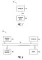
- FIG. 5illustrates a simplified block diagram of a controller coupled to an electronic device, according to various embodiments of the invention.
- FIG. 6illustrates an electronic system having devices formed in accordance with various embodiments of the invention.
- wafer and substrateas used in the following description may include any structure having an exposed surface with which to form an integrated circuit (IC) structure.
- substrateis understood to include semiconductor wafers.
- substrateis also used to refer to semiconductor structures during processing, and may include other layers that have been fabricated thereupon. Both “wafer” and “substrate” include doped and undoped semiconductors, epitaxial semiconductor layers supported by a base semiconductor or insulator, as well as other semiconductor structures well known to one skilled in the art.
- conductoris understood to generally include n-type and p-type semiconductors and the term “insulator” or “dielectric” is defined to include any material that is less electrically conductive than the materials referred to as conductors.
- horizontalas used in this application is defined as a plane parallel to the conventional plane or surface of a wafer or substrate, regardless of the orientation of the wafer or substrate.
- verticalrefers to a direction perpendicular to the horizontal as defined above. Prepositions, such as “on”, “side” (as in “sidewall”), “higher”, “lower”, “over” and “under” are defined with respect to the conventional plane or surface being on the top surface of the wafer or substrate, regardless of the orientation of the wafer or substrate.
- the two issues discussed above of dielectric integrity and charge trapping efficiencymay be addressed by the use of nano-particles of conductive materials at an interface of two dielectric materials.
- An analogymight be to think of the layer of nano-particles as replacing the floating gate electrode in a flash device.
- the efficiency of charge carrier transfer through the dielectric layersmay be adjusted to improve performance.
- the issue of reducing and scaling the size of the overall transistormay be addressed by increasing the dielectric constant of one or more of the dielectric layers, since an increase in the dielectric constant by a factor of two results in twice as much capacitive coupling between the gate electrode and the channel region. In effect, doubling the dielectric constant on a specific thickness dielectric layer results in a gate that operates as if it had a dielectric layer that was half the thickness, which results in improved device performance.
- a gate dielectric in a transistorhas both a physical gate dielectric thickness and an equivalent oxide thickness (EOT or t eq ).
- the equivalent oxide thickness (EOT)quantifies the electrical properties, such as capacitance, of the high-k gate dielectric in terms of a representative physical thickness of a silicon dioxide gate dielectric.
- the term t eqis defined as the thickness of a theoretical SiO 2 layer that would be needed to have the same capacitance density as a given dielectric, ignoring leakage current and reliability considerations.
- a SiO 2 layer of thickness, t, deposited on a Si surface as a gate dielectricwill have a t eq larger than its thickness, t.
- This t eqresults from the capacitance in the surface channel on which the SiO 2 is deposited due to the formation of a depletion/inversion region.
- This depletion/inversion regioncan result in t eq being from 0.3 to 0.6 nm larger than the physical SiO 2 thickness, t.
- the physical thickness requirement for a SiO 2 layer used for a gate dielectricwould need to be approximately 0.4 to 0.7 nm.
- Additional requirements for a SiO 2 gate dielectric layermay depend on the properties of the gate electrode used in conjunction with the SiO 2 gate dielectric. Using a conventional polysilicon gate would result in an additional increase in t eq for the SiO 2 layer. This additional thickness may be reduced by using a metal gate electrode, though metal gates are not currently used in typical complementary metal-oxide-semiconductor (CMOS) field effect transistor technology. Thus, future devices may require a physical SiO 2 gate dielectric layer of about 0.5 nm or less. Such a small thickness requirement for a SiO 2 oxide layer creates additional problems such as current leakage across the thin dielectric.
- CMOScomplementary metal-oxide-semiconductor
- Silicon dioxideis commonly used as a gate dielectric due to its electrical isolation properties in a SiO 2 —Si based structure. This electrical isolation is due to the relatively large band gap of SiO 2 (8.9 eV), making it a good electrical insulator. Significant reductions in its band gap would cause SiO 2 to become a poor material for a gate dielectric. As the thickness of a SiO 2 layer decreases, the number of atomic layers, or monolayers of the material decreases. At a certain thickness the number of monolayers will be sufficiently few that the SiO 2 layer will not have as complete an arrangement of atoms as found in a thicker (known as bulk) layer.
- a thin SiO 2 layer of only one or two monolayerswill not form a full band gap.
- Lack of a full band gap in a SiO 2 gate dielectricmay cause an effective short between an underlying conductive silicon channel and an overlying polysilicon gate.
- This undesirable propertysets a limit on the minimum physical thickness to which a SiO 2 layer can be scaled.
- the minimum thickness due to this monolayer effectis thought to be about 0.7 nm. Therefore, for future devices to have a t eq less than about 1.0 nm, dielectrics other than SiO 2 need to be considered for use as a gate dielectric.
- materials with a dielectric constant greater than that of SiO 2will have a physical thickness that may be larger than a desired t eq , while providing the desired equivalent oxide thickness.
- a dielectric material with a dielectric constant of 10such as Al 2 O 3
- a thickness of about 25.6 ⁇to provide a t eq of 1.0 nm, not including any depletion or inversion layer effects.
- a reduced equivalent oxide thickness for transistorscan be realized by using dielectric materials with higher dielectric constants than SiO 2 .
- EOTequivalent oxide thickness
- the dielectric on the silicon layerthere exists the possibility that a small layer of SiO 2 may be formed in addition to the desired dielectric.
- the resultwould effectively be a dielectric layer consisting of two sub-layers in parallel with each other and with the silicon layer on which the dielectric is formed.
- the resulting capacitancewould be that of two dielectrics in series.
- the t eqis again limited by a SiO 2 layer.
- the t eqwould be limited by the layer with the lowest dielectric constant.
- a desirable feature of the new higher constant dielectricwould be an oxygen barrier to prevent a layer of SiO 2 from forming on the silicon surface.
- SiO 2as a gate dielectric
- Having an amorphous structure for a gate dielectricprovides reduced leakage current problems associated with grain boundaries in polycrystalline gate dielectrics, which may cause high leakage paths. Grain size and orientation changes throughout a polycrystalline gate dielectric may cause variations in the film's dielectric constant, along with uniformity and surface topography problems, such as non-uniformity and roughness.
- materials having a high dielectric constant relative to SiO 2also have the disadvantage of existing in a crystalline form, at least in a bulk configuration.
- the best candidates for replacing SiO 2 as a gate dielectricare those with high dielectric constants, which can be fabricated as a thin layer with an amorphous form that can remain amorphous during the thermal cycles typically found in semiconductor production after the growth of the gate dielectric, such as gate electrode growth, metal deposition, and annealing operations.
- Tin oxides, such as SnO 2when alloyed with other oxides have been shown to raise the oxide crystallization temperature, and thus stabilize the long term interfacial characteristics of the amorphous dielectric at temperatures up to 1000° C.
- Candidates to replace SiO 2include materials with high dielectric constants (high k), a large energy gap (E g ), large energy barrier heights with the silicon substrate for both electrons and holes, and an amorphous nature that resists crystallization during the thermal cycling typically found in semiconductor manufacturing.
- High dielectric constant materialsmay be defined as having a dielectric constant greater than about twice the dielectric constant of silicon dioxide.
- the band gapis inversely related to the dielectric constant for a high k material, which lessens some benefits of the high dielectric constant material because of the potential leakage.
- High dielectric constant dielectric candidates for replacing silicon oxide as the dielectric material in electronic components in integrated circuitsinclude the lanthanide oxides such as Gd 2 O 3 , Ce 2 O 3 , La 2 O 3 , Pr 2 O 3 , Nd 2 O 3 , Sm 2 O 3 , Dy 2 O 3 , Tb 2 O 3 , Er 2 O 3 , Eu 2 O 3 , Lu 2 O 3 , Tm 2 O 3 , HO 2 O 3 , Pm 2 O 3 , and Yb 2 O 3 .
- Other candidatesinclude various lanthanide silicates, titanium oxide TiO 2 , hafnium oxide HfO 2 , and zirconium oxide, ZrO 2 .
- Such high dielectric constant layersprovide a significantly thinner equivalent oxide thickness compared with a silicon oxide layer having the same physical thickness.
- such dielectric layersprovide a significantly thicker physical thickness than a silicon oxide layer having the same equivalent oxide thickness. This increased physical thickness aids in reducing leakage current.
- Another consideration for selecting the material and method for forming a dielectric film for use in electronic devices and systemsconcerns the roughness of a dielectric film on a substrate. Surface roughness of the dielectric film has a significant effect on the electrical properties of the gate oxide and the resulting operating characteristics of the transistor.
- the leakage current through a physical 1.0 nm gate dielectricmay increase by a factor of 10 for every 0.1 increase in the root-mean-square (RMS) roughness of the dielectric layer.
- ALDatomic layer deposition
- Hafnium oxide (HfO 2 )a widely studied material, has a dielectric constant of about 20, a bandgap of around 5.6 eV, and conduction band/valence band offsets versus silicon of 2.0 eV/2.5 eV.
- hafnium oxideA potential issue with hafnium oxide is that oxygen may diffuse through the hafnium oxide during subsequent furnace operations and form a SiO 2 layer underneath the hafnium oxide at the silicon interface, resulting in reduced capacitive coupling between the gate electrode and the semiconductor.
- the leakage across the dielectric filmranges between 10 ⁇ 7 A/cm 2 to 1.0 ⁇ 10 ⁇ 9 A/cm 2 , depending upon the composition, which may form useful dielectric layers for semiconductor device gate insulators.
- ALDatomic layer deposition
- Hf Y O 2 filmwhere 0.5 ⁇ Y ⁇ 2.0, may have a selectable dielectric constant ranging from 15 to 22 depending primarily upon the value of Y and on the deposition temperature.
- a 10 nm thick layer of hafnium oxidewould have an equivalent oxide thickness (EOT) of about 2.0 nm, but being much thicker that the equivalent layer of silicon dioxide would have much lower leakage currents.
- EOTequivalent oxide thickness
- the use of ALDresults in dielectric layers grown on silicon surfaces having improved surface smoothness of around 0.10 nm root mean square (RMS) value on a 10 nm thick layer, resulting in less electric field concentration at insulator corners and projections, and again lower leakage currents. Further, forming such a dielectric film using atomic layer deposition can provide for controlling transitions between different material layers.
- ALD deposited dielectric filmsmay have an engineered transition with a substrate surface, or may be formed of many thin layers of different dielectric materials to enable selection of the dielectric constant to a value that is between the values obtainable from pure dielectric compounds.
- ALDwhich may be known as atomic layer epitaxy (ALE)
- ALEatomic layer epitaxy
- CVDchemical vapor deposition
- alternatively pulsed-CVDor “sequentially pulsed-CVD.”
- gaseous precursorsare introduced one at a time to the substrate surface mounted within a reaction chamber (or reactor). This introduction of the gaseous precursors takes the form of individual pulses of each gaseous precursor.
- the precursor gasis made to flow into a specific area or region for a short period of time.
- the reaction chamberis purged with a gas, which in many cases is an inert gas, and may also be evacuated prior to the next step.
- the first precursorsaturates and is chemisorbed (or adsorbed) at the substrate surface during the first pulsing phase.
- Subsequent pulsing with a purging gasremoves excess precursor from the reaction chamber, specifically the precursor that has not been chemisorbed.
- the second pulsing phaseintroduces a second precursor chemical (which may also be known as a reactant chemical) to the substrate where the growth reaction of the desired film takes place, with a reaction thickness that depends upon the amount of chemisorbed first precursor. Subsequent to the film growth reaction, reaction byproducts and precursor excess are purged from the reaction chamber. With a precursor chemistry where the precursors adsorb and aggressively react with each other on the substrate, one ALD cycle can be performed in less than one second in a flow type reaction chamber. Typically, precursor pulse times range from about 0.5 sec to about 2 to 3 seconds.
- ALDALD processes, the saturation of all the reaction and purging phases makes the film growth self-limiting. This self-limiting growth results in large area uniformity and conformality, which has important applications for such cases as planar substrates, deep trenches, and in the processing of porous silicon and high surface area silica and alumina powders.
- ALDprovides for controlling film thickness in a straightforward manner by controlling the number of growth cycles.
- ALDwas originally developed to manufacture luminescent and dielectric films needed in electroluminescent displays, such as doped zinc sulfide and alkaline earth metal sulfide films.
- ALDcan also grow different epitaxial II-V and II-VI films, non-epitaxial crystalline or amorphous oxide and nitride films, pure metal layers, alloy metal layers, and nanometer thick individual layers stacked in a multilayer structure, which may be known as a nanolaminant.
- the precursors used in an ALD processmay be gaseous, liquid or solid; however, liquid or solid precursors should be volatile with a vapor pressure high enough for effective mass transportation.
- solid and some liquid precursorsmay need to be heated inside the reaction chamber and introduced through heated tubes to the substrates.
- the desired vapor pressureshould be reached at a temperature below the substrate temperature to avoid the condensation of the precursors on the substrate. Due to the self-limiting growth mechanisms of ALD, relatively low vapor pressure solid precursors can be used, though evaporation rates may vary during the process because of changes in solid surface area.
- the precursors used in ALDshould be thermally stable at the substrate temperature because their decomposition would destroy the surface control and accordingly the benefit of the ALD method that relies on the reaction of the precursor at the substrate surface. A slight decomposition, if slow compared to the ALD growth, can be tolerated.
- the precursorsshould chemisorb on, or react with, the surface, though the interaction between the precursor and the surface as well as the mechanism for the adsorption is different for different precursors.
- the molecules at the substrate surfaceshould react aggressively with the second precursor, which may be called a reactant, to form the desired solid film. Additionally, precursors should not react with the film to cause etching, and precursors should not dissolve in the film.
- the ability to use highly reactive precursors in ALDcontrasts with the selection of precursors for conventional CVD type reactions.
- the by-products in the reactionshould be gaseous to allow their easy removal from the reaction chamber during a purge stage. Further, the by-products should not react or adsorb on the surface.
- the self-limiting process sequenceinvolves sequential surface chemical reactions.
- ALDrelies on chemistry between a reactive surface and one or more reactive molecular precursors, which are pulsed into the ALD reaction chamber separately.
- the metal precursor reaction at the substrateis typically followed by an inert gas pulse (or purge) to remove excess precursor and by-products from the reaction chamber prior to an input pulse of the next precursor of the fabrication sequence.
- filmscan be layered in equal metered sequences that are all identical in chemical kinetics, deposition per cycle, composition, and thickness.
- ALD sequencesgenerally deposit less than a full layer per cycle. Typically, a deposition or growth rate of about 0.25 to 2.00 ⁇ per cycle can be realized.
- ALD depositionsover other deposition techniques, such as CVD, include continuity at an interface avoiding poorly defined nucleating regions that are typical for thin chemical vapor deposition ( ⁇ 20 ⁇ ) and physical vapor deposition ( ⁇ 50 ⁇ ), conformality over a variety of substrate topologies due to its layer-by-layer deposition technique, use of low temperature and mildly oxidizing processes, lack of dependence on the reaction chamber, growth thickness dependent solely on the number of cycles performed, and ability to engineer multilayer laminate films with resolution of one to two monolayers.
- ALD processesallow for deposition control on the order of single monolayers and the ability to deposit amorphous films.
- a cycle of a deposition sequenceincludes pulsing a first precursor material, pulsing a purging gas for the precursor, pulsing a second reactant precursor, and pulsing the reactant's purging gas, resulting in a very consistent deposition thickness that depends upon the amount of the first precursor that adsorbs onto, and saturates, the surface.
- This cyclemay be repeated until the desired thickness is achieved in a single material dielectric layer, or may be alternated with pulsing a third precursor material, pulsing a purging gas for the third precursor, pulsing a fourth reactant precursor, and pulsing the reactant's purging gas.
- a nanolaminatemeans a composite film of ultra thin layers of two or more different materials in a layered stack, where the layers are alternating layers of the different materials having a thickness on the order of a nanometer, and may be a continuous film a single monolayer thick of the material.
- the nanolayersare not limited to alternating single layers of each material, but may include several layers of one material alternating with a single layer of the other material, to obtain a desired ratio of the two or more materials. Such an arrangement may obtain a dielectric constant that is between the values of the two materials taken singly.
- the dielectric layermay be formed of single layers of the two or more materials deposited individually, but the overall layer may act as a single film formed of an alloy of the individual films. This may depend upon the particular materials being used and their physical and chemical properties relative to one another. If the materials are miscible, the result may be a single dielectric layer or alloy.
- ALDatomic layer deposition
- Nano-particle devicesmay be used to replace a single floating gate electrode in a nonvolatile memory, such as a flash memory, to address the reliability issues with multiple dielectric layers separating two or more conductive electrodes.
- the material of the nano-particlesmay be chosen to adjust the work function desired for moving electrons or holes across the metal oxide layers, and the equivalent oxide thickness (EOT) of the overall dielectric layer may be reduced, as compared to the two insulator layers found in flash devices (i.e., one below the floating gate electrode and one between the floating gate and the control gate electrode).
- EOTequivalent oxide thickness
- each one of the two surfaces of each insulator layermay be in contact with a conductive surface, since each insulator layer may be located between solid conductive layers such as the substrate, the floating gate, and the control gate, so that a single defect in either insulator layer may cause a device failure in a floating gate device.
- metal oxide layer defectsmay have less effect in a nano-particle device since the insulators may be in contact with each other between the nano-particles and since the nano-particle layer may not be continuous. Nano-particles have diameters in the nanometer range.
- transistor dimensionsWhen transistor dimensions are scaled downward, the properties of a nonvolatile memory transistor tend to follow those of a volatile transistor, including operating faster and with lower total power dissipation, with lower threshold and operating voltages.
- the time the signal carriers (either electrons or holes) spend in the channel regiondecreases and the speed of the transistor increases. Reducing the lateral dimensions of a transistor also increases the electric field strength that the signal carriers encounter, which may result in faster carrier velocity and increased transistor speed; a lower operating voltage may sometimes also be used.
- a transistorsuch as the gate insulator (for example a silicon dioxide) thickness
- the gate insulatorfor example a silicon dioxide
- Reducing the vertical dimensions of a transistor, such as the gate insulator thicknessalso tends to increase the electric field strength at a selected gate voltage, which may lower the threshold voltage for the transistor, which may in turn increase the channel conductance, as well as increasing transistor reliability.
- reducing the gate insulator thicknessmay also result in defective devices and poor insulator properties with increased leakage.
- An embodiment of a method to form a semiconductor device that is less sensitive to dielectric defect levels, has improved charge storage efficiency, and is more easily reduced in dimensionmay include comprising forming a dielectric layer having a layer of a high work function metal and a layer of a metal oxide on a surface of a substrate, and forming a conductive layer on the dielectric layer, to complete the formation of an active device.
- the methodmay include forming the dielectric layer using atomic layer deposition to obtain a smoother and more uniform surface and a more accurate layer thickness.
- the metal oxidemay include a metal selected from titanium (Ti), zirconium (Zr) and Hafnium (Hf).
- the methodmay include forming a layer of silicon dioxide (SiO 2 ) having a first thickness, forming a layer of gold (Au) having a second thickness, and forming a layer of hafnium oxide (HfO 2 ) having a third thickness, to provide a relatively high-k overall dielectric layer, and all three layers may be formed using ALD to obtain improved control, and the dielectric layer may be amorphous after exposure to temperatures of up to 900° C.
- SiO 2silicon dioxide
- Augold
- HfO 2hafnium oxide
- the high work function metal layeris formed at an interface between the first silicon oxide and the hafnium oxide.
- the work functionmay be defined as the amount of energy needed to remove an electron from an atom, and may roughly be about half the ionization energy of a free atom.
- the work function from the substrate to the gate electrodemay be about 4.15 eV, while for a metal gate transistor the work function may be about 4.2 eV for aluminum and 4.5 eV for tungsten.
- a high work function materialsuch as gold may be about 4.8 to 5.1 eV, and platinum may have a work function of about 6.3 eV.
- the high work function metal layermay be formed of gold in one embodiment and may be formed as a layer on the silicon dioxide about 1 nm in thickness. After various heat treatments the layer may form individual nano-particles having an average diameter of less than 5 nm, which may be used as part of a gate dielectric layer forming a transistor, a capacitor, or a non-volatile memory device.
- the dielectricmay be formed to have an equivalent oxide thickness of less than 1.0 nm and a root mean square surface roughness less than one percent of the dielectric layer thickness.
- the methodmay include forming the dielectric layers and the metal nano-particle layer by chemical vapor deposition, an atomic layer deposition, a physical deposition, sputtering, evaporation, or a combination of these methods. For example, the silicon oxide may be thermally grown, the gold layer thermally evaporated, and the hafnium oxide formed by atomic layer deposition.
- Another embodimentmay include forming a first dielectric layer, such as silicon dioxide, on a surface of a substrate by atomic layer deposition, including exposing a surface at a selected temperature to a first precursor material for a time period and flow volume sufficient to saturate the substrate surface with the first precursor material. The surface is then exposed to a purge for a time sufficient to remove substantially all of a non-adsorbed portion of the first precursor material from the substrate surface. The substrate surface is then exposed to a reactant material to react with the adsorbed portion of the first precursor material on the surface to form a first dielectric layer having an intermediate thickness. The surface may then undergo another purge to remove any non-reacted portion of the first reactant material and any gaseous reaction byproducts from the substrate surface. The deposition steps are repeated for a selected number of cycles until a desired oxide thickness is reached.
- a first dielectric layersuch as silicon dioxide
- the methodmay further include forming a layer of a metal such as doped silicon, germanium, gold, or platinum, which may be formed by evaporation, sputtering, or atomic layer deposition on the first dielectric layer.
- a metalsuch as doped silicon, germanium, gold, or platinum, which may be formed by evaporation, sputtering, or atomic layer deposition on the first dielectric layer.
- the selected metalmay have a high work function, such as gold.
- a second dielectric layersuch as hafnium oxide, may then be formed by atomic layer deposition, similar to the method for forming the first oxide layer, but using a second temperature that may be different from the first temperature, and a second precursor material that may be different from the first precursor since it is likely that the second dielectric layer will have different desired properties.
- a precursor for the first dielectric layermay include silane, dichlorosilane and silicon tetrachloride, and a reactant may include oxygen, ozone, water, hydrogen peroxide, nitrogen dioxide and nitrous oxide.
- a precursormay include hafnium tetrachloride, hafnium tetraiodide, and anhydrous hafnium nitrate, with a reactant of water, oxygen, and hydrogen peroxide.
- the purge materialsmay be the same material, flow time period, and flow rate.
- the first temperaturemay be between 340 to 375 deg C.
- the second temperaturebetween 160 to 340 deg C.
- the precursor and reactant flow timesmay be from 0.3 seconds to 3.0 seconds.
- Another embodimentmay include forming a semiconductive device by forming a memory array with a dielectric structure containing a layer of a high work function metal and a layer of a metal oxide in an integrated circuit and depositing a conductive material contacting the dielectric structure to form an active device such as a capacitor, transistor or non-volatile memory cell.
- An address decodermay be formed coupled to the memory array to complete the operational device.
- the dielectric structuremay include a first layer of silicon oxide, a second layer of high work function nano-particles, and a third layer of hafnium oxide with a dielectric constant of about 22 to provide a very thin equivalent oxide layer for faster operation.
- An embodimentmay include a device having a semiconductive substrate with a dielectric layer formed of a first insulator material on a portion of the substrate with a first thickness, a high work function material (such as a metal, semiconductor or certain metal oxides) with a second thickness formed on the first insulator, a third layer formed of another insulator material having a third thickness formed on the first insulator and the high work function material, and a conductive material formed on the third layer, such as polysilicon, metals or refractory metals.
- a high work function materialsuch as a metal, semiconductor or certain metal oxides
- the first materialmay be silicon oxide having a thickness less than 1.0 nm
- the second materialmay be gold having a thickness of less than 1.0 nm
- the third materialmay be hafnium oxide with a dielectric constant of greater than 22, and an equivalent silicon dioxide thickness of less than 1.0 nm. This may provide a reliable gate dielectric layer that has the equivalent performance of a much thinner silicon dioxide layer.
- the devicecould have nano-particles of gold at the interface between the first and third insulators, each having a diameter of less than 5.0 nm, and a density of greater than 3.0 ⁇ 10 12 cm ⁇ 2 , and the dielectric layer is preferably amorphous.
- An embodimentmay include an electronic device with an amorphous dielectric structure having silicon dioxide, gold nano-particles, and a metal oxide such as titanium, zirconium, and hafnium.
- the devicehas a conductive layer on the dielectric layer.
- An embodimentmay include a system having a controller and an electronic device coupled to the controller.
- the electronic devicemay have a dielectric structure with one layer of silicon dioxide, a layer of gold nano-particles, and a layer of hafnium metal oxide as part of an integrated circuit, wherein the dielectric structure forms a non-volatile memory cell.
- the hafnium metal oxidefurther has a formula of Hf X O Y , with Y selected to provide a dielectric constant value of about 22 and a band gap value of about 5.6 eV, since a low bandgap may affect the insulation properties of the portion of the dielectric layer formed of hafnium oxide.
- the first dielectric layermay alternatively be formed of SiO 2 , other silicon oxides or other insulator materials such as metal oxides, metal carbides, and metal oxycarbides. Silicon dioxide layers may have a band-gap of about 8.9 eV, which would improve the leakage current over the 5.6 eV of hafnium oxide.
- the hafnium oxidemay be formed using ALD with hafnium tetrachloride (HfCl 4 ) as the precursor and water vapor at 350° C.
- the precursor, purge, and reactant timesare all 0.5 seconds, resulting in a hafnium oxide layer of 1.5 nm thickness per cycle.
- Another embodimentincludes forming an hafnium oxide using hafnium nitride, Hf(NO 3 ) 4 as the precursor at 300° C. with pulse times of 0.6 seconds, resulting in 0.36 nm films.
- Another embodimentincludes forming a HfO 2 layer using a hafnium tetrachloride (HfCl 4 ) precursor, performed at 300° C. with water vapor as the oxidizing reactant.
- a 0.5 second pulse of HfCl 4is followed by a 0.5 second purge with an inert gas, such as nitrogen, and a 0.5 second pulse of water vapor, resulting in a layer having a thickness of 0.15 nm.
- Another embodimentincludes deposition at 200° C., resulting in a thicker layer of hafnium oxide of 0.33 nm thickness.
- Yet another embodimentincludes using a precursor of hafnium tetraiodide at 300° C. with water vapor, resulting in a 0.45 nm layer thickness per cycle.
- An embodiment for forming silicon oxide by ALDmay include a precursor of silane at 300° C. with ozone as the oxidizing reactant, resulting in a 0.50 nm layer per deposition cycle.
- Other solid or liquid precursorsmay be used in an appropriately designed reaction chamber (also known as a reactor) for any of the above noted metals.
- the use of such precursors in an ALD reaction chambermay result in lower deposition temperatures in the range of 180° C. to 400° C., and the ability to use mildly oxidizing reactant materials such as H 2 O, H 2 O 2 , various alcohols, N 2 O, ozone or oxygen.
- Purge gasesmay include nitrogen, helium, argon or neon.
- reactantmeans a precursor material that is added to the ALD reactor to react with the previously introduced precursor material, to form a layer of the product material. It should be noted that there is no intrinsic difference between a precursor material and a reactant material other than the order in which they enter the reactor. The terms are used to facilitate understanding of the principles of the invention and are not used in a limiting sense.
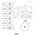
- FIG. 1shows an embodiment of an atomic layer deposition system 100 for forming a dielectric or metal layer containing gold and hafnium oxide.
- the elements depictedpermit discussion of the present invention such that those skilled in the art may practice the present invention without undue experimentation.
- a substrate 108 on a heating element/wafer holder 106is located inside a reaction chamber 102 of ALD system 100 .
- the heating element 106is thermally coupled to substrate 108 to control the substrate temperature.
- a gas-distribution fixture 110introduces precursor, reactant, and purge gases to the region of the surface of substrate 108 in a uniform fashion.
- the gases introduced by the gas distribution fixture(sometimes referred to as a showerhead, although other configurations may be easily imagined), react with the substrate 108 , with any excess precursor gas and reaction products removed from chamber 102 by vacuum pump 104 through a control valve 105 .
- the system 100may operate at any desired deposition pressure by controlling the volume of gas entering the chamber 102 as compared to the volume of gaseous reaction product and excess gases removed from the chamber 102 via control of the pumping rate of vacuum pump 104 , and the valve 105 .
- ALD systemsmay operate at normal atmospheric pressures, or may operate under essentially vacuum conditions, or anywhere in between.
- hafnium oxideis formed at a reduced pressure of 10 ⁇ 5 Torr pressure with oxygen gas providing the oxidation reactant.
- Each gasoriginates from individual gas sources 114 , 118 , 122 , 126 , 130 , and 134 , with a flow rate and time controlled by mass-flow controllers 116 , 120 , 124 , 128 , 132 , and 136 , respectively.
- the sources 118 , 122 , and 126provide the three precursor materials, either by storing the precursor as a gas or by providing a location and apparatus for evaporating a solid or liquid material to form the selected precursor gas by evaporation, sublimation, or entrainment in a gas stream.
- a single purging gas source 114is also included, although the invention is not so limited, and numerous different purge gases, such as nitrogen, argon, neon, hydrogen, and krypton may be used, individually, in combination, simultaneously, or sequentially.
- the purge gas source 114is coupled to mass-flow controller 116 .
- Two reactant material sources, 130 and 134are connected through mass-flow controllers 132 and 136 .
- the precursor, reactant, and purge gas sourcesare coupled by their associated mass-flow controllers to a common gas line or conduit 112 , which is coupled to the gas-distribution fixture 110 inside the reaction chamber 102 .
- Gas conduit 112may also be coupled to another vacuum pump, or exhaust pump, not shown, to remove excess precursor gases, purging gases, and by-product gases at the end of a purging sequence from the gas conduit 112 .
- Vacuum pump, or exhaust pump, 104is coupled to chamber 102 by control valve 105 , which may be a mass-flow valve, to remove excess precursor gases, purging gases, and by-product gases from reaction chamber 102 at the end of a purging sequence.
- control valve 105may be a mass-flow valve, to remove excess precursor gases, purging gases, and by-product gases from reaction chamber 102 at the end of a purging sequence.
- control displays, mounting apparatus, temperature sensing devices, substrate maneuvering apparatus, and electrical connections as are known to those skilled in the artare not shown in FIG. 1 . Though illustrated ALD system 100 is suited for practicing the present invention, other commercially available ALD systems may also be used.
- reaction chambers for deposition of filmsare understood by those of ordinary skill in the art of semiconductor fabrication.
- the present inventionmay be practiced on a variety of such reaction chambers without undue experimentation, or by use of CVD, evaporation or sputtering equipment.
- detection, measurement, and control techniques in the art of semiconductor fabricationupon reading the disclosure.
- the elements of ALD system 100may be controlled by a computer. To focus on the use of ALD system 100 in the various embodiments of the present invention, the computer is not shown. Those skilled in the art can appreciate that the individual elements such as pressure control, temperature control, and gas flow within ALD system 100 can be computer controlled.
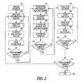
- FIG. 2illustrates a flow diagram of operational steps for an embodiment of a general method to form a layer by ALD.
- the individual films forming the final filmmay be dielectric or metal layers, and may be stoichiometric pure films, such as HfO 2 , or may be non-stoichiometric, as the final film may have any ratio of components.
- a substrateis prepared to react immediately with, and chemisorb (or adsorb) the first precursor gas.
- This preparationwill remove contaminants such as thin organic films, dirt, and native oxide from the surface of the substrate, and may include a hydrofluoric acid rinse or sputter etch in the reaction chamber 102 of FIG. 1 .
- a first precursor materialenters the reaction chamber for a predetermined length of time, for example from 0.5-2.0 seconds, preferably 1.0 seconds.
- Various hafnium-containing gases, liquids, and sublimating solidsmay be used, as discussed previously, in the described embodiment where the silicon oxide layer is formed by thermal oxidation and the gold layer is formed by evaporation.
- the final filmmay be free of carbon, hydrogen, or halogen contamination.
- the first precursor materialis chemically adsorbed (chemisorbed) onto the surface of the substrate, the amount depending at least in part upon the temperature of the substrate, for example 300° C., and at least in part on the presence of sufficient flow of the precursor material.
- a first purge gasenters the reaction chamber for a predetermined length of time sufficient to remove substantially all the non-chemisorbed first precursor material. Typical times may be 1.0-2.0 seconds, with a purge gas comprising nitrogen, argon, neon, hydrogen, and combinations thereof.
- a first reactant gasenters the chamber for a predetermined length of time, sufficient to provide enough of the reactant material to chemically combine with the amount of chemisorbed first precursor material on the surface of the substrate.
- the reactant material for the first precursorcomprises water vapor (i.e., H 2 O) for a pulse length of 0.60 seconds.
- Typical reactant materialsinclude mildly oxidizing materials, including, but not limited to, water vapor, hydrogen peroxide, nitrogen oxides, ozone, oxygen gas, various plasmas of the same, and combinations thereof.
- a second purge gaswhich may be the same or different from the first purge gas, enters the chamber for a predetermined time, sufficient to remove substantially all non-reacted materials and any reaction byproducts from the chamber.
- the thickness of the HfO 2 layer obtained from a single ALD cycleis 0.33 nm. If another deposition cycle is needed to reach the desired thickness, the operation returns to 204 and repeats the deposition process until the desired first dielectric layer is completed, at which time the process moves on to the deposition of the second material at 214 .
- a second precursor material for the second materialenters the reaction chamber for a predetermined length of time, typically 0.5-2.0 seconds.
- the second precursor materialis chemically adsorbed onto the surface of the substrate, in this case the top surface of the first material, the amount of absorption depending upon the temperature of the substrate and the presence of sufficient flow of the precursor material.
- the pulsing of the precursormay use a pulsing period that provides uniform coverage of an adsorbed monolayer on the substrate surface, or may use a pulsing period that provides partial formation of a monolayer on the substrate surface.
- a purge gasenters the chamber, which is illustrated as being the same as the first purge gas, but the invention is not so limited.
- the purge gas used in the second material depositionmay be the same or different from either of the two previously noted purge gases, and FIG. 1 could be shown as having more than the one purge gas source shown.
- the purge cyclecontinues for a predetermined time sufficient to remove substantially all of the non-chemisorbed second precursor material.
- a second reactant gaswhich may the same or different from the first reactant gas, enters the chamber for a predetermined length of time, sufficient to provide enough of the reactant to chemically combine with the amount of chemisorbed second precursor material on the surface of the substrate.
- another purge gasenters the chamber, which may be the same or different from any of the three previously discussed purge gases, for a predetermined time sufficient to remove non-reacted materials and any reaction byproducts from the chamber.
- the desired thicknesses of the first and second materialsmay not be the same, and there may be more deposition cycles for one material than for the other.
- the processmoves on to 224 , where a third precursor is pulsed into the reaction chamber (or reactor).
- the third precursorchemisorbs onto the surface.
- the illustrative embodimenthas a particular order of precursors, which is for illustration only; the invention is not so limited, and any of the three discussed precursors may be used in any order, in accordance with desired layer characteristics.
- the third reactantis pulsed into the reactor.
- the third reactantmay be the same as the previous reactants, or the third reactant may be a different material, and in an embodiment is water vapor pulsed for 0.20 seconds.
- another purgeoccurs as before.
- the desired thicknesses of the first, second, and third materialsmay not be the same thickness, and there may be more deposition cycles for one material as compared to the other. If the third material has reached the desired thickness the operation moves to 234 , where it is determined if the first, second, and third dielectric materials have reached the desired number for the finished structure. In the described embodiments there are only a single layer of each of the three layers and thus the general ALD case of returning to deposit further layers of the first material will not occur.
- the processmoves back to another deposition of the first dielectric material at 204 .
- the depositionends at 236 .
- the present illustrative embodimentdiscusses and illustrates the layers as distinct from each other, the individual layers are very thin and may effectively act as a single alloy layer. Subsequent heat cycles may alloy the individual layers into a single dielectric layer.
- the present embodimenthas the hafnium oxide layer deposited first, but the invention is not so limited.
- the ALD processcan be implemented to form transistors, capacitors, memory devices, and other electronic systems including information handling devices.
- the inventionis not limited to the described three materials.
- FIG. 3illustrates a single transistor in an embodiment of a method to form a dielectric layer containing an ALD deposited silicon oxide, gold, and hafnium oxide layer.
- a substrate 302is prepared for deposition, typically a silicon or silicon-containing material; however, other semiconductor materials such as germanium, gallium arsenide, and silicon-on-sapphire substrates may also be used.
- This preparation processincludes cleaning substrate 302 and forming various layers and regions of the substrate, such as drain diffusion 304 and source diffusion 306 of an illustrative metal oxide semiconductor (MOS) transistor 300 , prior to forming a gate dielectric.
- MOSmetal oxide semiconductor
- the substrate 302is typically cleaned to provide an initial substrate depleted of its native oxide, since the presence of a thin layer of SiO 2 will result in decreased capacitive coupling as discussed previously.
- the substratemay also be cleaned to provide a hydrogen-terminated surface to improve the rate of chemisorption.
- a silicon substratemay undergo a final hydrofluoric (HF) acid rinse prior to ALD processing to provide the silicon substrate with a hydrogen-terminated surface without a native silicon oxide layer.
- HFhydrofluoric
- Cleaning preceding atomic layer depositionaids in reducing the presence of silicon oxide at an interface between the silicon-based substrate and the dielectric formed using the atomic layer deposition process.
- the sequencing of the formation of the regions of the transistor being processedmay follow typical sequencing that is generally performed in the fabrication of a MOS transistor, as is well known to those skilled in the art.
- the dielectric covering the area on the substrate 302 between the source and drain diffused regions 304 and 306is deposited by ALD in this illustrative embodiment, and comprises silicon oxide layer 308 , a gold layer 312 , and a hafnium layer 316 .
- This multilayer structurewhich acts as a dielectric even with a gold layer 312 disposed between the two dielectric layers 308 and 316 , may be referred to as the gate oxide.
- the illustrative embodimentalso shows the top and bottom dielectric layers 308 and 316 as having the same thickness, however the desired dielectric properties of the gate oxide may be achieved by adjusting the dielectric thickness ratios to different values. Even though the illustrative embodiment shows the various layers 308 , 312 , and 316 as being distinct from one another, the gate oxide 314 overall functionally appears as a single dielectric layer.
- the transistor 300has a conductive material forming a single gate electrode 318 which may be formed of polysilicon, aluminum, tungsten, metal silicides, or any other conductive material.
- a conductive materialforming a single gate electrode 318 which may be formed of polysilicon, aluminum, tungsten, metal silicides, or any other conductive material.
- Use of dielectric layers containing atomic layer deposited dielectric layers for a gate dielectricis not limited to silicon-based substrates but may be used with a variety of semiconductor substrates.
- a methodincludes forming a first conductive layer 402 , a second conductive layer 404 , and a dielectric having dielectric layer 406 , gold nano-particle layer 410 , and high-k dielectric layer 414 , formed of at least three different materials, formed between the two conductive layers.
- the conductive layers 402 and 404may be formed of metals, doped polysilicon, silicided metals, polycides, or conductive organic compounds, without affecting the teaching of this embodiment.
- Transistors, capacitors, and other devices having dielectric filmsmay be implemented into memory devices and electronic systems including information handling devices.
- Embodiments of these information handling devicesmay include wireless systems, telecommunication systems, computers, and integrated circuits.
- FIG. 5illustrates a simplified diagram for an illustrative electronic system 500 having one or more devices including a dielectric layer containing nano-particles in a memory device or non-volatile memory device according to various disclosed embodiments.
- the electronic system 500may include a controller 502 , a bus 504 , and an electronic device 506 , where bus 504 provides electrical conductivity between controller 502 and electronic device 506 .
- the controller 502 and/or electronic device 506may include a non-volatile memory device as previously discussed herein.
- Electronic system 500may include information handling, wireless, telecommunication, fiber optic, automotive, electro-optic, mobile electronics, handheld devices, and computer systems.
- Electronic device 506may comprise a microprocessor, a floating point unit, an arithmetic logic unit, a memory device, a multiplexer, an address decoder, a power controller, or any other electronic device used in computer, telecommunication, sensor, display, and other products.
- FIG. 6depicts a diagram of an electronic system 600 having at least one device formed in accordance to the disclosed embodiments, including a controller 602 and a memory 606 .
- Controller 602 and/or memory 606may include a non-volatile memory device.
- the system 600may also include an electronic apparatus 608 and a bus 604 , where the bus 604 may provide electrical conductivity and data transmission between controller 602 and electronic apparatus 608 , and between controller 602 and memory 606 .
- the bus 604may include an address, a data bus, and a control bus, each independently configured.
- the bus 604may use common conductive lines for providing address, data, and/or control, the use of which may be regulated by the controller 602 .
- the electronic apparatus 608may include additional memory devices configured similar to the memory 606 . Some embodiments may include an additional peripheral device 610 coupled to the bus 604 .
- the controller 602comprises a processor. Any of the controller 602 , the memory 606 , the bus 604 , the electronic apparatus 608 , and peripheral devices 610 may include a memory device (e.g., similar to the device 506 of FIG. 5 ) in accordance with the disclosed embodiments.
- System 600may include, but is not limited to, information handling devices, telecommunication systems, mobile electronic devices such as laptop computers, handheld personal electronic devices such as personal digital assistants (PDA) and palm tops, handheld communication devices such as cell phones, digital cameras and DVD recorders, and computers.
- Peripheral devices 610may include displays, additional storage memory, or other control devices that may operate in conjunction with controller 602 and/or memory 606 .
- the described transistor arrangementmay be used in an NROM type device, a DRAM (Dynamic Random Access Memory), SRAM (Static Random Access Memory) or flash memory.
- the DRAMmay comprise a synchronous DRAM commonly referred to as SGRAM (Synchronous Graphics Random Access Memory), SDRAM (Synchronous Dynamic Random Access Memory), SDRAM II, and DDR SDRAM (Double Data Rate SDRAM), as well as Synchlink or Rambus DRAMs and other emerging DRAM technologies.
- the dielectric layer thicknessmay be selected to determine the overall threshold voltage of the transistor containing the dielectric structure.
- Some embodimentsmay include transistors, electronic devices, memory devices, electronic systems, and personal electronic systems having nonvolatile memory transistors constructed according to the various embodiments contained herein.
Landscapes
- Engineering & Computer Science (AREA)
- Condensed Matter Physics & Semiconductors (AREA)
- Crystallography & Structural Chemistry (AREA)
- General Chemical & Material Sciences (AREA)
- Physics & Mathematics (AREA)
- Chemical Kinetics & Catalysis (AREA)
- Chemical & Material Sciences (AREA)
- General Physics & Mathematics (AREA)
- Manufacturing & Machinery (AREA)
- Computer Hardware Design (AREA)
- Microelectronics & Electronic Packaging (AREA)
- Power Engineering (AREA)
- Formation Of Insulating Films (AREA)
- Semiconductor Memories (AREA)
Abstract
Description
t=(k/kox)teq=(k/3.9)teq.
Thus, materials with a dielectric constant greater than that of SiO2, (about 3.9), will have a physical thickness that may be larger than a desired teq, while providing the desired equivalent oxide thickness. For example, a dielectric material with a dielectric constant of 10, such as Al2O3, could have a thickness of about 25.6 Å to provide a teqof 1.0 nm, not including any depletion or inversion layer effects. Thus, a reduced equivalent oxide thickness for transistors can be realized by using dielectric materials with higher dielectric constants than SiO2.
teq=tSiO
Thus, if a SiO2layer is formed in the process, the teqis again limited by a SiO2layer. In the event that a barrier layer is formed between the silicon layer and the desired dielectric in which the barrier layer prevents the formation of a SiO2layer, the teqwould be limited by the layer with the lowest dielectric constant. Thus a desirable feature of the new higher constant dielectric would be an oxygen barrier to prevent a layer of SiO2from forming on the silicon surface. Whether a single dielectric layer with a high dielectric constant or a barrier layer with a higher dielectric constant than SiO2is employed, the layer directly in contact with or interfacing with the silicon layer must provide a high quality interface to maintain high channel carrier mobility.
Claims (20)
Priority Applications (1)
| Application Number | Priority Date | Filing Date | Title |
|---|---|---|---|
| US13/757,290US9064866B2 (en) | 2007-06-04 | 2013-02-01 | High-k dielectrics with gold nano-particles |
Applications Claiming Priority (2)
| Application Number | Priority Date | Filing Date | Title |
|---|---|---|---|
| US11/810,004US8367506B2 (en) | 2007-06-04 | 2007-06-04 | High-k dielectrics with gold nano-particles |
| US13/757,290US9064866B2 (en) | 2007-06-04 | 2013-02-01 | High-k dielectrics with gold nano-particles |
Related Parent Applications (1)
| Application Number | Title | Priority Date | Filing Date |
|---|---|---|---|
| US11/810,004DivisionUS8367506B2 (en) | 2007-06-04 | 2007-06-04 | High-k dielectrics with gold nano-particles |
Publications (2)
| Publication Number | Publication Date |
|---|---|
| US20130153986A1 US20130153986A1 (en) | 2013-06-20 |
| US9064866B2true US9064866B2 (en) | 2015-06-23 |
Family
ID=40087141
Family Applications (2)
| Application Number | Title | Priority Date | Filing Date |
|---|---|---|---|
| US11/810,004Active2028-08-05US8367506B2 (en) | 2007-06-04 | 2007-06-04 | High-k dielectrics with gold nano-particles |
| US13/757,290Active2027-07-24US9064866B2 (en) | 2007-06-04 | 2013-02-01 | High-k dielectrics with gold nano-particles |
Family Applications Before (1)
| Application Number | Title | Priority Date | Filing Date |
|---|---|---|---|
| US11/810,004Active2028-08-05US8367506B2 (en) | 2007-06-04 | 2007-06-04 | High-k dielectrics with gold nano-particles |
Country Status (1)
| Country | Link |
|---|---|
| US (2) | US8367506B2 (en) |
Families Citing this family (20)
| Publication number | Priority date | Publication date | Assignee | Title |
|---|---|---|---|---|
| US7927948B2 (en) | 2005-07-20 | 2011-04-19 | Micron Technology, Inc. | Devices with nanocrystals and methods of formation |
| US8367506B2 (en) | 2007-06-04 | 2013-02-05 | Micron Technology, Inc. | High-k dielectrics with gold nano-particles |
| JP4594973B2 (en)* | 2007-09-26 | 2010-12-08 | 株式会社東芝 | Nonvolatile semiconductor memory device |
| US7858535B2 (en)* | 2008-05-02 | 2010-12-28 | Micron Technology, Inc. | Methods of reducing defect formation on silicon dioxide formed by atomic layer deposition (ALD) processes and methods of fabricating semiconductor structures |
| TWI398952B (en)* | 2009-11-19 | 2013-06-11 | Ind Tech Res Inst | Transistor |
| KR20110103534A (en)* | 2010-03-15 | 2011-09-21 | 삼성전자주식회사 | Method of forming dielectric film structure, capacitor manufacturing method and capacitor using same |
| KR101943077B1 (en)* | 2012-12-12 | 2019-04-17 | 한국전자통신연구원 | A transistor hanving nano layer structured oxides and method of manufacturing the same |
| US9187314B2 (en) | 2013-03-15 | 2015-11-17 | Robert Bosch Gmbh | Anisotropic conductor and method of fabrication thereof |
| US9233842B2 (en)* | 2013-03-15 | 2016-01-12 | Robert Bosch Gmbh | Passivation layer for harsh environments and methods of fabrication thereof |
| US20150008428A1 (en) | 2013-07-08 | 2015-01-08 | Semiconductor Energy Laboratory Co., Ltd. | Semiconductor device and method for manufacturing semiconductor device |
| US9666697B2 (en)* | 2013-07-08 | 2017-05-30 | Semiconductor Energy Laboratory Co., Ltd. | Semiconductor device and method for manufacturing semiconductor device including an electron trap layer |
| US9449853B2 (en) | 2013-09-04 | 2016-09-20 | Semiconductor Energy Laboratory Co., Ltd. | Method for manufacturing semiconductor device comprising electron trap layer |
| US9735359B2 (en)* | 2014-04-23 | 2017-08-15 | Micron Technology, Inc. | Methods of forming a memory cell material, and related methods of forming a semiconductor device structure, memory cell materials, and semiconductor device structures |
| US10319675B2 (en)* | 2016-01-13 | 2019-06-11 | Taiwan Semiconductor Manufacturing Company, Ltd. | Capacitor embedded with nanocrystals |
| US10145009B2 (en)* | 2017-01-26 | 2018-12-04 | Asm Ip Holding B.V. | Vapor deposition of thin films comprising gold |
| CN107699954B (en)* | 2017-09-29 | 2020-03-20 | 中国科学院光电技术研究所 | Strong-coupling gold nano superlattice structure and self-assembly preparation method thereof |
| KR20210016476A (en)* | 2018-06-29 | 2021-02-15 | 램 리써치 코포레이션 | Oxidative conversion in the atomic layer deposition process |
| CN116390641A (en)* | 2020-06-18 | 2023-07-04 | 中国科学院微电子研究所 | HfO (HfO) 2 Preparation method of base ferroelectric capacitor |
| US11764221B2 (en)* | 2020-07-30 | 2023-09-19 | Taiwan Semiconductor Manufacturing Co., Ltd. | Semiconductor device and method of manufacture |
| CN119984380B (en)* | 2024-12-25 | 2025-08-22 | 北京大学 | A flexible proximity and pressure sensor based on fringe field effect and its preparation method |
Citations (233)
| Publication number | Priority date | Publication date | Assignee | Title |
|---|---|---|---|---|
| US3571918A (en) | 1969-03-28 | 1971-03-23 | Texas Instruments Inc | Integrated circuits and fabrication thereof |
| US5149596A (en) | 1990-10-05 | 1992-09-22 | The United States Of America As Represented By The United States Department Of Energy | Vapor deposition of thin films |
| US5434878A (en) | 1994-03-18 | 1995-07-18 | Brown University Research Foundation | Optical gain medium having doped nanocrystals of semiconductors and also optical scatterers |
| US5455489A (en) | 1994-04-11 | 1995-10-03 | Bhargava; Rameshwar N. | Displays comprising doped nanocrystal phosphors |
| US5516588A (en) | 1991-03-27 | 1996-05-14 | Widia Gmbh | Composite body, its use and a process for its production |
| US5585020A (en) | 1994-11-03 | 1996-12-17 | Becker; Michael F. | Process for the production of nanoparticles |
| US5652061A (en) | 1995-05-22 | 1997-07-29 | Lucent Technologies Inc. | Devices comprising films of β-C3 N4 |
| US5662834A (en) | 1995-07-21 | 1997-09-02 | Hydro-Quebec | Alloys of Ti Ru Fe and O and use thereof for the manufacture of cathodes for the electrochemical synthesis of sodium chlorate |
| US5714766A (en) | 1995-09-29 | 1998-02-03 | International Business Machines Corporation | Nano-structure memory device |
| US5714336A (en) | 1986-08-05 | 1998-02-03 | Hoechst Aktiengesellschaft | Process and test kit for determining free active compounds in biological fluids |
| US5770022A (en) | 1997-06-05 | 1998-06-23 | Dow Corning Corporation | Method of making silica nanoparticles |
| US5772760A (en) | 1991-11-25 | 1998-06-30 | The University Of Chicago | Method for the preparation of nanocrystalline diamond thin films |
| US5851880A (en) | 1996-06-14 | 1998-12-22 | Oki Electric Industry Co., Ltd. | Method of making nonvolatile memory elements with selector transistors |
| US5874134A (en) | 1996-01-29 | 1999-02-23 | Regents Of The University Of Minnesota | Production of nanostructured materials by hypersonic plasma particle deposition |
| US5882779A (en) | 1994-11-08 | 1999-03-16 | Spectra Science Corporation | Semiconductor nanocrystal display materials and display apparatus employing same |
| US5939146A (en) | 1996-12-11 | 1999-08-17 | The Regents Of The University Of California | Method for thermal spraying of nanocrystalline coatings and materials for the same |
| US5989511A (en) | 1991-11-25 | 1999-11-23 | The University Of Chicago | Smooth diamond films as low friction, long wear surfaces |
| US6025034A (en) | 1995-11-13 | 2000-02-15 | University Of Connecticut And Rutgers | Method of manufacture of nanostructured feeds |
| US6060743A (en) | 1997-05-21 | 2000-05-09 | Kabushiki Kaisha Toshiba | Semiconductor memory device having multilayer group IV nanocrystal quantum dot floating gate and method of manufacturing the same |
| US6063705A (en) | 1998-08-27 | 2000-05-16 | Micron Technology, Inc. | Precursor chemistries for chemical vapor deposition of ruthenium and ruthenium oxide |
| USRE36760E (en) | 1993-11-16 | 2000-07-04 | Sandia Corporation | Method and apparatus for altering material using ion beams |
| US6129928A (en) | 1997-09-05 | 2000-10-10 | Icet, Inc. | Biomimetic calcium phosphate implant coatings and methods for making the same |
| US6140181A (en) | 1997-11-13 | 2000-10-31 | Micron Technology, Inc. | Memory using insulator traps |
| USH1924H (en) | 1998-09-15 | 2000-12-05 | The United States Of America As Represented By The Secretary Of The Air Force | Load-adaptive nanocrystalline carbon/amorphous diamond-like carbon composite and preparation method |
| US6162712A (en) | 1995-06-30 | 2000-12-19 | Advanced Technology Materials, Inc. | Platinum source compositions for chemical vapor deposition of platinum |
| US6174677B1 (en) | 1995-10-13 | 2001-01-16 | Ut-Battelle, Llc | Advanced surface-enhanced Raman gene probe systems and methods thereof |
| US6184550B1 (en) | 1998-08-28 | 2001-02-06 | Advanced Technology Materials, Inc. | Ternary nitride-carbide barrier layers |
| US6194237B1 (en) | 1997-12-16 | 2001-02-27 | Hyundai Electronics Industries Co., Ltd. | Method for forming quantum dot in semiconductor device and a semiconductor device resulting therefrom |
| US6208881B1 (en) | 1998-10-20 | 2001-03-27 | Micropure Medical, Inc. | Catheter with thin film electrodes and method for making same |
| US20010012698A1 (en) | 1999-08-02 | 2001-08-09 | Symetrix Corporation | Metal oxide thin films for high dielectric constant application |
| US6291341B1 (en) | 1999-02-12 | 2001-09-18 | Micron Technology, Inc. | Method for PECVD deposition of selected material films |
| US6291314B1 (en) | 1998-06-23 | 2001-09-18 | Silicon Genesis Corporation | Controlled cleavage process and device for patterned films using a release layer |
| US6297095B1 (en) | 2000-06-16 | 2001-10-02 | Motorola, Inc. | Memory device that includes passivated nanoclusters and method for manufacture |
| US6313015B1 (en) | 1999-06-08 | 2001-11-06 | City University Of Hong Kong | Growth method for silicon nanowires and nanoparticle chains from silicon monoxide |
| US6317175B1 (en) | 1990-12-31 | 2001-11-13 | Kopin Corporation | Single crystal silicon arrayed devices with optical shield between transistor and substrate |
| US6331282B1 (en) | 1997-11-10 | 2001-12-18 | Board Of Regents, The University Of Texas System | Manganese oxyiodides and their method of preparation and use in energy storage |
| US20020003252A1 (en) | 1998-09-03 | 2002-01-10 | Ravi Iyer | Flash memory circuit with with resistance to disturb effect |
| US20020013052A1 (en) | 2000-03-08 | 2002-01-31 | Visokay Mark R. | Methods for preparing ruthenium metal films |
| US6346477B1 (en) | 2001-01-09 | 2002-02-12 | Research Foundation Of Suny - New York | Method of interlayer mediated epitaxy of cobalt silicide from low temperature chemical vapor deposition of cobalt |
| US6346189B1 (en) | 1998-08-14 | 2002-02-12 | The Board Of Trustees Of The Leland Stanford Junior University | Carbon nanotube structures made using catalyst islands |
| US20020037320A1 (en) | 2000-06-14 | 2002-03-28 | Denes Ferencz S. | Method and apparatus for producing colloidal nanoparticles in a dense medium plasma |
| US20020046993A1 (en) | 2000-10-24 | 2002-04-25 | Peterson Dennis Roger | Electrothermal gun for direct electrothermal-physical conversion of precursor into nanopowder |
| US6414543B1 (en) | 2000-11-28 | 2002-07-02 | Precision Dynamics Corporation | Rectifying charge storage element |
| US6447848B1 (en) | 1995-11-13 | 2002-09-10 | The United States Of America As Represented By The Secretary Of The Navy | Nanosize particle coatings made by thermally spraying solution precursor feedstocks |
| US6447764B1 (en) | 1997-08-21 | 2002-09-10 | Degussa Ag | Method for isolating anionic organic substances from aqueous systems using cationic polymer nanoparticles |
| US6458431B2 (en) | 2000-07-28 | 2002-10-01 | Ekc Technology, Inc. | Methods for the lithographic deposition of materials containing nanoparticles |
| US6472632B1 (en) | 1999-09-15 | 2002-10-29 | Nanoscale Engineering And Technology Corporation | Method and apparatus for direct electrothermal-physical conversion of ceramic into nanopowder |
| US20020187091A1 (en) | 2001-06-11 | 2002-12-12 | Deevi Seetharama C. | Coking and carburization resistant iron aluminides for hydrocarbon cracking |
| US6495436B2 (en) | 2001-02-09 | 2002-12-17 | Micron Technology, Inc. | Formation of metal oxide gate dielectric |
| US20020192366A1 (en) | 2001-01-30 | 2002-12-19 | Cramer Ronald Dean | Method of hydrophilizing materials |
| US20020190251A1 (en) | 2001-03-13 | 2002-12-19 | Toyoki Kunitake | Thin film materials of amorphous metal oxides |
| US20020193040A1 (en) | 2001-06-18 | 2002-12-19 | Zhou Otto Z. | Method of making nanotube-based material with enhanced electron field emission properties |
| US20020197793A1 (en) | 2000-01-06 | 2002-12-26 | Dornfest Charles N | Low thermal budget metal oxide deposition for capacitor structures |
| US20030001190A1 (en) | 2000-11-09 | 2003-01-02 | Micron Technology, Inc. | Methods for forming conductive structures and structures regarding same |
| US6514828B2 (en) | 2001-04-20 | 2003-02-04 | Micron Technology, Inc. | Method of fabricating a highly reliable gate oxide |
| US20030030074A1 (en) | 2001-08-13 | 2003-02-13 | Walker Andrew J | TFT mask ROM and method for making same |
| US20030045078A1 (en) | 2001-08-30 | 2003-03-06 | Micron Technology, Inc. | Highly reliable amorphous high-K gate oxide ZrO2 |
| US6534420B2 (en) | 2001-07-18 | 2003-03-18 | Micron Technology, Inc. | Methods for forming dielectric materials and methods for forming semiconductor devices |
| US6572836B1 (en) | 2000-03-17 | 2003-06-03 | Hydro-Quebec | Method for producing gaseous hydrogen by chemical reaction of metals or metal hydrides subjected to intense mechanical deformations |
| US20030108612A1 (en) | 2001-10-31 | 2003-06-12 | Xu Xiaohong Nancy | Metallic nanoparticles for inhibition of bacterium growth |
| US6580124B1 (en) | 2000-08-14 | 2003-06-17 | Matrix Semiconductor Inc. | Multigate semiconductor device with vertical channel current and method of fabrication |
| US6587408B1 (en) | 1998-10-01 | 2003-07-01 | Massachusetts Institute Of Technology | High-density mechanical memory and turing machine |
| US6586785B2 (en) | 2000-06-29 | 2003-07-01 | California Institute Of Technology | Aerosol silicon nanoparticles for use in semiconductor device fabrication |
| US6592839B2 (en) | 1991-11-25 | 2003-07-15 | The University Of Chicago | Tailoring nanocrystalline diamond film properties |
| US20030143801A1 (en) | 1999-09-01 | 2003-07-31 | Cem Basceri | Method of reducing oxygen vacancies and DRAM processing method |
| US20030148577A1 (en) | 2002-02-06 | 2003-08-07 | Merkulov Vladimir I. | Controlled alignment of catalytically grown nanostructures in a large-scale synthesis process |
| US20030152700A1 (en) | 2002-02-11 | 2003-08-14 | Board Of Trustees Operating Michigan State University | Process for synthesizing uniform nanocrystalline films |
| US20030162587A1 (en) | 2002-02-28 | 2003-08-28 | Kabushiki Kaisha Toshiba | Random number generating device |
| US20030161782A1 (en) | 2001-07-20 | 2003-08-28 | Young-Nam Kim | Preparation of carbon nanotubes |
| US20030183901A1 (en) | 2001-05-09 | 2003-10-02 | Hitachi, Ltd. | MOS transistor apparatus and method of manufacturing same |
| US20030185983A1 (en) | 1998-04-02 | 2003-10-02 | Max-Planck-Gesellschaft Zur Forderung Der Wissenschaften E. V. | Device for specific particle manipulation and deposition |
| US20030183306A1 (en) | 1994-08-01 | 2003-10-02 | Franz Hehmann | Selected processing for non-equilibrium light alloys and products |
| US20030196513A1 (en) | 2002-04-18 | 2003-10-23 | Jonathan Phillips | Method for producing metallic microparticles |
| US6638575B1 (en) | 2000-07-24 | 2003-10-28 | Praxair Technology, Inc. | Plasma sprayed oxygen transport membrane coatings |
| US6656792B2 (en) | 2001-10-19 | 2003-12-02 | Chartered Semiconductor Manufacturing Ltd | Nanocrystal flash memory device and manufacturing method therefor |
| US20030228747A1 (en) | 2002-06-05 | 2003-12-11 | Micron Technology, Inc. | Pr2O3-based la-oxide gate dielectrics |
| US20030231992A1 (en) | 2002-06-17 | 2003-12-18 | Sarkas Harry W. | Process for preparing nanostructured materials of controlled surface chemistry |
| US20030235076A1 (en) | 2002-06-21 | 2003-12-25 | Micron Technology, Inc. | Multistate NROM having a storage density much greater than 1 Bit per 1F2 |
| US20030235066A1 (en) | 2002-06-21 | 2003-12-25 | Micron Technology, Inc. | Ferroelectric write once read only memory for archival storage |
| US20030235064A1 (en) | 2002-06-21 | 2003-12-25 | Shubneesh Batra | Method of forming a non-volatile electron storage memory and the resulting device |
| US20030234420A1 (en) | 2002-06-21 | 2003-12-25 | Micron Technology, Inc. | Write once read only memory with large work function floating gates |
| US6669996B2 (en) | 2000-07-06 | 2003-12-30 | University Of Louisville | Method of synthesizing metal doped diamond-like carbon films |
| WO2004000728A1 (en) | 2002-06-24 | 2003-12-31 | Honda Giken Kogyo Kabushiki Kaisha | Method for making carbon nanotubes |
| US20040009118A1 (en) | 2002-07-15 | 2004-01-15 | Jonathan Phillips | Method for producing metal oxide nanoparticles |
| US20040014060A1 (en) | 2000-05-05 | 2004-01-22 | Werner Hoheisel | Doped nanoparticles as biolabels |
| US6689192B1 (en) | 2001-12-13 | 2004-02-10 | The Regents Of The University Of California | Method for producing metallic nanoparticles |
| US20040042128A1 (en) | 2002-08-30 | 2004-03-04 | Slaughter Jon M. | Nanocrystalline layers for improved MRAM tunnel junctions |
| US20040043569A1 (en) | 2002-08-28 | 2004-03-04 | Ahn Kie Y. | Atomic layer deposited HfSiON dielectric films |
| US20040046130A1 (en) | 2000-07-19 | 2004-03-11 | Rao Nagaraja P | Apparatus and method for synthesizing films and coatings by focused particle beam deposition |
| US20040058385A1 (en) | 2000-11-17 | 2004-03-25 | Abel Andreas Peter | Kit and method for determining multiple analytes, with provisions for refrencing the density of immobilised recognition elements |
| US20040055892A1 (en) | 2001-11-30 | 2004-03-25 | University Of North Carolina At Chapel Hill | Deposition method for nanostructure materials |
| US6713812B1 (en) | 2002-10-09 | 2004-03-30 | Motorola, Inc. | Non-volatile memory device having an anti-punch through (APT) region |
| US6713329B1 (en) | 1999-05-10 | 2004-03-30 | The Trustees Of Princeton University | Inverter made of complementary p and n channel transistors using a single directly-deposited microcrystalline silicon film |
| US20040065171A1 (en) | 2002-10-02 | 2004-04-08 | Hearley Andrew K. | Soild-state hydrogen storage systems |
| US20040086897A1 (en) | 2002-05-07 | 2004-05-06 | Mirkin Chad A. | Nanoparticle probes with Raman Spectroscopic fingerprints for analyte detection |
| US20040094801A1 (en) | 2002-11-20 | 2004-05-20 | Motorola, Inc. | Ferromagnetic semiconductor structure and method for forming the same |
| US20040105807A1 (en) | 2002-11-29 | 2004-06-03 | Shoushan Fan | Method for manufacturing carbon nanotubes |
| US6746893B1 (en) | 1997-07-29 | 2004-06-08 | Micron Technology, Inc. | Transistor with variable electron affinity gate and methods of fabrication and use |
| US20040107906A1 (en) | 2000-08-11 | 2004-06-10 | Applied Materials, Inc. | Plasma immersion ion implantation apparatus including a plasma source having low dissociation and low minimum plasma voltage |
| US20040110347A1 (en) | 2002-05-28 | 2004-06-10 | Matsushita Electric Industrial Co. Ltd. | Method of production of nanoparticle and nanoparticle produced by the method of production |
| US6756292B2 (en) | 2001-09-21 | 2004-06-29 | Samsung Electronics Co., Ltd. | Method of forming a quantum dot and a gate electrode using the same |
| US20040126649A1 (en) | 2002-12-30 | 2004-07-01 | Jin-Ming Chen | Simple procedure for growing highly-ordered nanofibers by self-catalytic growth |
| US20040127001A1 (en) | 2002-12-27 | 2004-07-01 | International Business Machines Corporation | Robust ultra-low k interconnect structures using bridge-then-metallization fabrication sequence |
| US20040130951A1 (en) | 2002-06-21 | 2004-07-08 | Micron Technology, Inc. | Write once read only memory employing charge trapping in insulators |
| US20040131865A1 (en) | 2002-07-22 | 2004-07-08 | Kim George E. | Functional coatings for the reduction of oxygen permeation and stress and method of forming the same |
| US20040131795A1 (en) | 2002-12-27 | 2004-07-08 | National Chiao Tung University | Method to control the magnetic alloy-encapsulated carbon-base nanostructures |
| US20040135997A1 (en) | 2002-06-12 | 2004-07-15 | Selena Chan | Metal coated nanocrystalline silicon as an active surface enhanced raman spectroscopy (SERS) substrate |
| US20040135951A1 (en) | 2002-09-30 | 2004-07-15 | Dave Stumbo | Integrated displays using nanowire transistors |
| US6764874B1 (en) | 2003-01-30 | 2004-07-20 | Motorola, Inc. | Method for chemical vapor deposition of single walled carbon nanotubes |
| US6767419B1 (en) | 2000-11-09 | 2004-07-27 | Bechtel Bwxt Idaho, Llc | Methods of forming hardened surfaces |
| US6767795B2 (en) | 2002-01-17 | 2004-07-27 | Micron Technology, Inc. | Highly reliable amorphous high-k gate dielectric ZrOXNY |
| US20040147098A1 (en) | 2002-11-22 | 2004-07-29 | Frederic Mazen | Method for forming, by CVD, nanostructures of semi-conductor material of homogeneous and controlled size on dielectric material |
| US20040144980A1 (en) | 2003-01-27 | 2004-07-29 | Ahn Kie Y. | Atomic layer deposition of metal oxynitride layers as gate dielectrics and semiconductor device structures utilizing metal oxynitride layers |
| US20040149759A1 (en) | 2001-04-25 | 2004-08-05 | Moser Eva Maria | Gastight container |
| US20040158028A1 (en) | 2001-05-08 | 2004-08-12 | Buehler Friedrich Severin | Polyamide moulding compounds for producing optical lenses |
| US20040160830A1 (en) | 2001-08-30 | 2004-08-19 | Micron Technology, Inc. | DRAM cells with repressed floating gate memory, low tunnel barrier interpoly insulators |
| US20040175882A1 (en) | 2003-03-04 | 2004-09-09 | Micron Technology, Inc. | Atomic layer deposited dielectric layers |
| EP1462415A2 (en) | 2003-03-26 | 2004-09-29 | Canon Kabushiki Kaisha | Production process of nano carbon material |
| US20040202032A1 (en) | 2002-06-21 | 2004-10-14 | Micron Technology, Inc. | Vertical NROM having a storage density of 1 bit per 1F2 |
| US20040206957A1 (en) | 2000-07-11 | 2004-10-21 | Seiko Epson Corporation | Semiconductor device and method of manufacture |
| US20040212426A1 (en) | 2000-11-28 | 2004-10-28 | Beigel Michael L. | Rectifying charge storage device with sensor |
| US20040214399A1 (en) | 2003-04-22 | 2004-10-28 | Micron Technology, Inc. | Atomic layer deposited ZrTiO4 films |
| US6815781B2 (en) | 2001-09-25 | 2004-11-09 | Matrix Semiconductor, Inc. | Inverted staggered thin film transistor with salicided source/drain structures and method of making same |
| US20040224505A1 (en) | 2001-09-10 | 2004-11-11 | Tegal Corporation | Nanolayer thick film processing system and method |
| US20040245085A1 (en) | 2002-03-13 | 2004-12-09 | Gopalakrishnan Srinivasan | Process and synthesizer for molecular engineering and synthesis of materials |
| US6831310B1 (en) | 2003-11-10 | 2004-12-14 | Freescale Semiconductor, Inc. | Integrated circuit having multiple memory types and method of formation |
| US20040258192A1 (en) | 2003-06-16 | 2004-12-23 | General Electric Company | Mitigation of steam turbine stress corrosion cracking |
| US20040266107A1 (en) | 2003-06-27 | 2004-12-30 | Chindalore Gowrishankar L. | Non-volatile memory having a reference transistor and method for forming |
| US6839280B1 (en) | 2003-06-27 | 2005-01-04 | Freescale Semiconductor, Inc. | Variable gate bias for a reference transistor in a non-volatile memory |
| US6844203B2 (en) | 2001-08-30 | 2005-01-18 | Micron Technology, Inc. | Gate oxides, and methods of forming |
| US6844319B1 (en) | 1998-10-08 | 2005-01-18 | Stichting Voor De Technische Wetenschappen | Peptide-based carrier devices for stellate cells |
| US20050011748A1 (en) | 2001-08-25 | 2005-01-20 | Thomas Beck | Method for producing a nanostructured funcitonal coating and a coating that can be produced according to said method |
| US20050019836A1 (en) | 2000-12-06 | 2005-01-27 | Horst Vogel | Bioanalytical reagent, method for production thereof, sensor platforms and detection methods based on use of said bioanalytical reagent |
| US20050019365A1 (en) | 2001-04-02 | 2005-01-27 | Frauchiger Vinzenz M. | Bioactive surface layer, particularly for medical implants and prostheses |
| US6849948B2 (en) | 2003-03-05 | 2005-02-01 | Au Optronics Corporation | Contact structure and manufacturing method thereof |
| US20050031785A1 (en) | 2003-08-07 | 2005-02-10 | The University Of Chicago | Method to grow pure nanocrystalline diamond films at low temperatures and high deposition rates |
| US20050037374A1 (en) | 1999-11-08 | 2005-02-17 | Melker Richard J. | Combined nanotechnology and sensor technologies for simultaneous diagnosis and treatment |
| US20050035430A1 (en) | 2000-11-28 | 2005-02-17 | Beigel Michael L. | Rectifying charge storage element |
| US6859093B1 (en) | 2000-11-28 | 2005-02-22 | Precision Dynamics Corporation | Rectifying charge storage device with bi-stable states |
| US20050040034A1 (en) | 2001-12-06 | 2005-02-24 | Ralf Landgraf | Coating method and coating |
| US20050041455A1 (en) | 2000-11-28 | 2005-02-24 | Beigel Michael L. | Rectifying charge storage memory circuit |
| US20050048570A1 (en) | 2001-12-28 | 2005-03-03 | Fraunhofer-Gesellschaft Zur Forderung Der Angewandten | Structured-functional bonding matrices for biomolecules |
| US20050048796A1 (en) | 2003-08-29 | 2005-03-03 | Anelva Corporation | Forming method and a forming apparatus of nanocrystalline silicon structure |
| US20050048414A1 (en) | 2003-08-26 | 2005-03-03 | Oliver Harnack | Method for patterning organic materials or combinations of organic and inorganic materials |
| US20050053826A1 (en) | 2003-09-08 | 2005-03-10 | Intematix Corporation | Low platinum fuel cell catalysts and method for preparing the same |
| US20050064185A1 (en) | 2003-08-04 | 2005-03-24 | Nanosys, Inc. | System and process for producing nanowire composites and electronic substrates therefrom |
| US20050061785A1 (en) | 2003-09-24 | 2005-03-24 | Nanotechnologies, Inc. | Nanopowder synthesis using pulsed arc discharge and applied magnetic field |
| US20050061249A1 (en) | 2003-09-22 | 2005-03-24 | Fuji Xerox Co., Ltd. | Carbon nanotube manufacturing apparatus and method, and gas decomposer for use in the manufacturing apparatus and method |
| US6887758B2 (en) | 2002-10-09 | 2005-05-03 | Freescale Semiconductor, Inc. | Non-volatile memory device and method for forming |
| US6893984B2 (en) | 2002-02-20 | 2005-05-17 | Micron Technology Inc. | Evaporated LaA1O3 films for gate dielectrics |
| US6896617B2 (en) | 2003-07-08 | 2005-05-24 | Bally Gaming International, Inc. | Multi-reel slot machine with selectable reel play |
| US6900122B2 (en) | 2001-12-20 | 2005-05-31 | Micron Technology, Inc. | Low-temperature grown high-quality ultra-thin praseodymium gate dielectrics |
| US20050151261A1 (en) | 2002-09-20 | 2005-07-14 | Kellar Scot A. | Ultra-high capacitance device based on nanostructures |
| US6921702B2 (en) | 2002-07-30 | 2005-07-26 | Micron Technology Inc. | Atomic layer deposited nanolaminates of HfO2/ZrO2 films as gate dielectrics |
| US20050170089A1 (en) | 2004-01-15 | 2005-08-04 | David Lashmore | Systems and methods for synthesis of extended length nanostructures |
| US6953730B2 (en) | 2001-12-20 | 2005-10-11 | Micron Technology, Inc. | Low-temperature grown high quality ultra-thin CoTiO3 gate dielectrics |
| US6958302B2 (en) | 2002-12-04 | 2005-10-25 | Micron Technology, Inc. | Atomic layer deposited Zr-Sn-Ti-O films using TiI4 |
| US6960538B2 (en) | 2002-08-21 | 2005-11-01 | Micron Technology, Inc. | Composite dielectric forming methods and composite dielectrics |
| US20050265063A1 (en) | 2004-02-24 | 2005-12-01 | Micron Technology, Inc. | 4F2 EEPROM NROM memory arrays with vertical devices |
| US20050285225A1 (en) | 2004-06-29 | 2005-12-29 | Ahn Kie Y | Semiconductor constructions comprising cerium oxide and titanium oxide |
| US6989573B2 (en) | 2003-10-10 | 2006-01-24 | Micron Technology, Inc. | Lanthanide oxide/zirconium oxide atomic layer deposited nanolaminate gate dielectrics |
| US20060024975A1 (en) | 2004-08-02 | 2006-02-02 | Micron Technology, Inc. | Atomic layer deposition of zirconium-doped tantalum oxide films |
| US20060038179A1 (en) | 2004-03-02 | 2006-02-23 | Ali Afzali-Ardakani | Method and apparatus for solution processed doping of carbon nanotube |
| US20060043504A1 (en) | 2004-08-31 | 2006-03-02 | Micron Technology, Inc. | Atomic layer deposited titanium aluminum oxide films |
| US20060046383A1 (en) | 2004-09-02 | 2006-03-02 | Shenlin Chen | Method for forming a nanocrystal floating gate for a flash memory device |
| US20060046522A1 (en) | 2004-08-31 | 2006-03-02 | Micron Technology, Inc. | Atomic layer deposited lanthanum aluminum oxide dielectric layer |
| US20060046384A1 (en) | 2004-08-24 | 2006-03-02 | Kyong-Hee Joo | Methods of fabricating non-volatile memory devices including nanocrystals |
| US20060067871A1 (en) | 2004-05-26 | 2006-03-30 | Massachusetts Institute Of Technology | Methods and devices for growth and/or assembly of nanostructures |
| US7037862B2 (en) | 2001-06-13 | 2006-05-02 | Micron Technology, Inc. | Dielectric layer forming method and devices formed therewith |
| US7037574B2 (en) | 2001-05-23 | 2006-05-02 | Veeco Instruments, Inc. | Atomic layer deposition for fabricating thin films |
| US7045430B2 (en) | 2002-05-02 | 2006-05-16 | Micron Technology Inc. | Atomic layer-deposited LaAlO3 films for gate dielectrics |
| US20060105523A1 (en) | 2004-11-18 | 2006-05-18 | International Business Machines Corporation | Chemical doping of nano-components |
| US7049192B2 (en) | 2003-06-24 | 2006-05-23 | Micron Technology, Inc. | Lanthanide oxide / hafnium oxide dielectrics |
| US20060118853A1 (en) | 2004-12-06 | 2006-06-08 | Asahi Glass Company, Limited | Nonvolatile semiconductor memory device having excellent charge retention and manufacturing process of the same |
| US20060128168A1 (en) | 2004-12-13 | 2006-06-15 | Micron Technology, Inc. | Atomic layer deposited lanthanum hafnium oxide dielectrics |
| US20060125030A1 (en) | 2004-12-13 | 2006-06-15 | Micron Technology, Inc. | Hybrid ALD-CVD of PrxOy/ZrO2 films as gate dielectrics |
| US7067840B2 (en) | 2001-10-30 | 2006-06-27 | Infineon Technologies Ag | Method and device for reducing the contact resistance in organic field-effect transistors by embedding nanoparticles to produce field boosting |
| US7068544B2 (en) | 2001-08-30 | 2006-06-27 | Micron Technology, Inc. | Flash memory with low tunnel barrier interpoly insulators |
| US20060140868A1 (en) | 2002-12-19 | 2006-06-29 | Stephanie Grancharov | Method of preparation of biomagnetic nanoparticles coated with a noble metal layer |
| US20060148180A1 (en) | 2005-01-05 | 2006-07-06 | Micron Technology, Inc. | Atomic layer deposited hafnium tantalum oxide dielectrics |
| US7081421B2 (en) | 2004-08-26 | 2006-07-25 | Micron Technology, Inc. | Lanthanide oxide dielectric layer |
| US7084078B2 (en) | 2002-08-29 | 2006-08-01 | Micron Technology, Inc. | Atomic layer deposited lanthanide doped TiOx dielectric films |
| US20060177975A1 (en) | 2005-02-10 | 2006-08-10 | Micron Technology, Inc. | Atomic layer deposition of CeO2/Al2O3 films as gate dielectrics |
| US20060176645A1 (en) | 2005-02-08 | 2006-08-10 | Micron Technology, Inc. | Atomic layer deposition of Dy doped HfO2 films as gate dielectrics |
| US20060189154A1 (en) | 2005-02-23 | 2006-08-24 | Micron Technology, Inc. | Atomic layer deposition of Hf3N4/HfO2 films as gate dielectrics |
| US20060194438A1 (en) | 2004-06-25 | 2006-08-31 | Rao Rajesh A | Method of forming a nanocluster charge storage device |
| US7101813B2 (en) | 2002-12-04 | 2006-09-05 | Micron Technology Inc. | Atomic layer deposited Zr-Sn-Ti-O films |
| US20060223337A1 (en) | 2005-03-29 | 2006-10-05 | Micron Technology, Inc. | Atomic layer deposited titanium silicon oxide films |
| US20060228868A1 (en) | 2005-03-29 | 2006-10-12 | Micron Technology, Inc. | ALD of amorphous lanthanide doped TiOx films |
| US20060231889A1 (en) | 2005-04-13 | 2006-10-19 | Tupei Chen | Two-terminal solid-state memory device and two-terminal flexible memory device based on nanocrystals or nanoparticles |
| US20060244100A1 (en) | 2005-04-28 | 2006-11-02 | Micron Technology, Inc. | Atomic layer deposited zirconium silicon oxide films |
| US20060244082A1 (en) | 2005-04-28 | 2006-11-02 | Micron Technology, Inc. | Atomic layer desposition of a ruthenium layer to a lanthanide oxide dielectric layer |
| US7132329B1 (en) | 2005-06-29 | 2006-11-07 | Freescale Semiconductor, Inc. | Source side injection storage device with spacer gates and method therefor |
| US20060252202A1 (en) | 2005-05-09 | 2006-11-09 | Jiyan Dai | Process and apparatus for fabricating nano-floating gate memories and memory made thereby |
| US7135421B2 (en) | 2002-06-05 | 2006-11-14 | Micron Technology, Inc. | Atomic layer-deposited hafnium aluminum oxide |
| US7138336B2 (en) | 2001-08-06 | 2006-11-21 | Asm Genitech Korea Ltd. | Plasma enhanced atomic layer deposition (PEALD) equipment and method of forming a conducting thin film using the same thereof |
| US20060263972A1 (en) | 2005-02-15 | 2006-11-23 | Micron Technology, Inc. | ATOMIC LAYER DEPOSITION OF Zr3N4/ZrO2 FILMS AS GATE DIELECTRICS |
| US20060270147A1 (en) | 2005-05-27 | 2006-11-30 | Micron Technology, Inc. | Hafnium titanium oxide films |
| US20060273411A1 (en) | 2005-06-07 | 2006-12-07 | Freescale Semiconductor, Inc. | In-situ nitridation of high-k dielectrics |
| US20060281330A1 (en) | 2005-06-14 | 2006-12-14 | Micron Technology, Inc. | Iridium / zirconium oxide structure |
| US7160577B2 (en) | 2002-05-02 | 2007-01-09 | Micron Technology, Inc. | Methods for atomic-layer deposition of aluminum oxides in integrated circuits |
| US20070018342A1 (en) | 2005-07-20 | 2007-01-25 | Micron Technology, Inc. | Devices with nanocrystals and methods of formation |
| US20070018214A1 (en) | 2005-07-25 | 2007-01-25 | Micron Technology, Inc. | Magnesium titanium oxide films |
| US20070049051A1 (en) | 2005-08-29 | 2007-03-01 | Micron Technology, Inc. | Atomic layer deposition of Zrx Hfy Sn1-x-y O2 films as high k gate dielectrics |
| US20070048989A1 (en) | 2005-08-30 | 2007-03-01 | Micron Technology, Inc. | Atomic layer deposition of GdScO3 films as gate dielectrics |
| US20070049054A1 (en) | 2005-08-31 | 2007-03-01 | Micron Technology, Inc. | Cobalt titanium oxide dielectric films |
| US20070048790A1 (en) | 2003-10-15 | 2007-03-01 | The Trustees Of Columbia University In The City Of New York | Device for measuring nanometer level pattern-dependent binding reactions |
| US20070049023A1 (en) | 2005-08-29 | 2007-03-01 | Micron Technology, Inc. | Zirconium-doped gadolinium oxide films |
| US20070048926A1 (en) | 2005-08-31 | 2007-03-01 | Micron Technology, Inc. | Lanthanum aluminum oxynitride dielectric films |
| US20070059645A1 (en) | 2005-06-16 | 2007-03-15 | The Trustees Of Columbia University In The City Of New York | Methods for fabricating nanoscale electrodes and uses thereof |
| US20070059775A1 (en) | 2005-03-29 | 2007-03-15 | The Trustees Of Columbia University In The City Of New York | Synthesis and conjugation of iron oxide nanoparticles to antibodies for targeting specific cells using fluorescence and MR imaging techniques |
| US7192824B2 (en) | 2003-06-24 | 2007-03-20 | Micron Technology, Inc. | Lanthanide oxide / hafnium oxide dielectric layers |
| US20070092989A1 (en) | 2005-08-04 | 2007-04-26 | Micron Technology, Inc. | Conductive nanoparticles |
| US20070140951A1 (en) | 2003-12-11 | 2007-06-21 | The Trustees Of Columbia University In The City Of New York | Nano-sized particles, processes of making, compositions and uses thereof |
| US20070228526A1 (en) | 2006-03-30 | 2007-10-04 | Kabushiki Kaisha Toshiba | Insulating film and semiconductor device |
| US20070228442A1 (en) | 2004-09-09 | 2007-10-04 | Tokyo Electron Limited | Thin Film Capacitor, Method for Forming Same, and Computer Readable Recording Medium |
| US20070287261A1 (en) | 2001-06-21 | 2007-12-13 | Asm International N.V. | Trench isolation structures for integrated circuits |
| US20080069760A1 (en) | 2004-06-04 | 2008-03-20 | The Trustees Of Columbia University In The City Of New York | Methods For Preparing Single -Walled Carbon Nanoturbes |
| US20080110486A1 (en) | 2006-11-15 | 2008-05-15 | General Electric Company | Amorphous-crystalline tandem nanostructured solar cells |
| US20080157171A1 (en) | 2006-12-29 | 2008-07-03 | Prashant Majhi | Dielectric barrier for nanocrystals |
| US20080217159A1 (en)* | 2007-03-05 | 2008-09-11 | Toyota Jidosha Kabushiki Kaisha | Decomposition method and decomposition apparatus for nucleic acid polymer |
| US20080224115A1 (en) | 2003-12-22 | 2008-09-18 | Erik Petrus Antonius Maria Bakkers | Fabricating a Set of Semiconducting Nanowires, and Electric Device Comprising a Set of Nanowires |
| US7432548B2 (en) | 2006-08-31 | 2008-10-07 | Micron Technology, Inc. | Silicon lanthanide oxynitride films |
| US20080246114A1 (en) | 2007-04-09 | 2008-10-09 | Freescale Semiconductor, Inc. | Integrated passive device with a high resistivity substrate and method for forming the same |
| US7435657B2 (en) | 2004-11-26 | 2008-10-14 | Samsung Electronics Co., Ltd | Method of fabricating transistor including buried insulating layer and transistor fabricated using the same |
| US20080296650A1 (en) | 2007-06-04 | 2008-12-04 | Micron Technology, Inc. | High-k dielectrics with gold nano-particles |
| US7482619B2 (en) | 2005-09-07 | 2009-01-27 | Samsung Electronics Co., Ltd. | Charge trap memory device comprising composite of nanoparticles and method of fabricating the charge trap memory device |
| US7498230B2 (en) | 2007-02-13 | 2009-03-03 | Micron Technology, Inc. | Magnesium-doped zinc oxide structures and methods |
| US20090075035A1 (en) | 2006-04-07 | 2009-03-19 | O'brien Stephen | Preparing nanoparticles and carbon nanotubes |
| US7517783B2 (en) | 2007-02-13 | 2009-04-14 | Micron Technology, Inc. | Molybdenum-doped indium oxide structures and methods |
| US7563730B2 (en) | 2006-08-31 | 2009-07-21 | Micron Technology, Inc. | Hafnium lanthanide oxynitride films |
| US20090236655A1 (en)* | 2005-12-01 | 2009-09-24 | Sam-Jong Choi | Integrated circuit device gate structures |
| US20100055830A1 (en)* | 2005-11-15 | 2010-03-04 | Macronix International Co., Ltd. | I-shaped phase change memory cell |
Family Cites Families (2)
| Publication number | Priority date | Publication date | Assignee | Title |
|---|---|---|---|---|
| US6458645B2 (en) | 1998-02-26 | 2002-10-01 | Micron Technology, Inc. | Capacitor having tantalum oxynitride film and method for making same |
| AU2001271370A1 (en)* | 2000-06-22 | 2002-01-02 | Vicon Industries, Inc. | Dome housed video camera assembly with 180 degree tilt motion |
- 2007
- 2007-06-04USUS11/810,004patent/US8367506B2/enactiveActive
- 2013
- 2013-02-01USUS13/757,290patent/US9064866B2/enactiveActive
Patent Citations (267)
| Publication number | Priority date | Publication date | Assignee | Title |
|---|---|---|---|---|
| US3571918A (en) | 1969-03-28 | 1971-03-23 | Texas Instruments Inc | Integrated circuits and fabrication thereof |
| US5714336A (en) | 1986-08-05 | 1998-02-03 | Hoechst Aktiengesellschaft | Process and test kit for determining free active compounds in biological fluids |
| US5149596A (en) | 1990-10-05 | 1992-09-22 | The United States Of America As Represented By The United States Department Of Energy | Vapor deposition of thin films |
| US6317175B1 (en) | 1990-12-31 | 2001-11-13 | Kopin Corporation | Single crystal silicon arrayed devices with optical shield between transistor and substrate |
| US5516588A (en) | 1991-03-27 | 1996-05-14 | Widia Gmbh | Composite body, its use and a process for its production |
| US5772760A (en) | 1991-11-25 | 1998-06-30 | The University Of Chicago | Method for the preparation of nanocrystalline diamond thin films |
| US5989511A (en) | 1991-11-25 | 1999-11-23 | The University Of Chicago | Smooth diamond films as low friction, long wear surfaces |
| US6592839B2 (en) | 1991-11-25 | 2003-07-15 | The University Of Chicago | Tailoring nanocrystalline diamond film properties |
| USRE36760E (en) | 1993-11-16 | 2000-07-04 | Sandia Corporation | Method and apparatus for altering material using ion beams |
| US5434878A (en) | 1994-03-18 | 1995-07-18 | Brown University Research Foundation | Optical gain medium having doped nanocrystals of semiconductors and also optical scatterers |
| US5455489A (en) | 1994-04-11 | 1995-10-03 | Bhargava; Rameshwar N. | Displays comprising doped nanocrystal phosphors |
| US20030183306A1 (en) | 1994-08-01 | 2003-10-02 | Franz Hehmann | Selected processing for non-equilibrium light alloys and products |
| US5585020A (en) | 1994-11-03 | 1996-12-17 | Becker; Michael F. | Process for the production of nanoparticles |
| US5882779A (en) | 1994-11-08 | 1999-03-16 | Spectra Science Corporation | Semiconductor nanocrystal display materials and display apparatus employing same |
| US5652061A (en) | 1995-05-22 | 1997-07-29 | Lucent Technologies Inc. | Devices comprising films of β-C3 N4 |
| US6162712A (en) | 1995-06-30 | 2000-12-19 | Advanced Technology Materials, Inc. | Platinum source compositions for chemical vapor deposition of platinum |
| US5662834A (en) | 1995-07-21 | 1997-09-02 | Hydro-Quebec | Alloys of Ti Ru Fe and O and use thereof for the manufacture of cathodes for the electrochemical synthesis of sodium chlorate |
| US5714766A (en) | 1995-09-29 | 1998-02-03 | International Business Machines Corporation | Nano-structure memory device |
| US6174677B1 (en) | 1995-10-13 | 2001-01-16 | Ut-Battelle, Llc | Advanced surface-enhanced Raman gene probe systems and methods thereof |
| US6447848B1 (en) | 1995-11-13 | 2002-09-10 | The United States Of America As Represented By The Secretary Of The Navy | Nanosize particle coatings made by thermally spraying solution precursor feedstocks |
| US6025034A (en) | 1995-11-13 | 2000-02-15 | University Of Connecticut And Rutgers | Method of manufacture of nanostructured feeds |
| US6277448B2 (en) | 1995-11-13 | 2001-08-21 | Rutgers The State University Of New Jersey | Thermal spray method for the formation of nanostructured coatings |
| US5874134A (en) | 1996-01-29 | 1999-02-23 | Regents Of The University Of Minnesota | Production of nanostructured materials by hypersonic plasma particle deposition |
| US5851880A (en) | 1996-06-14 | 1998-12-22 | Oki Electric Industry Co., Ltd. | Method of making nonvolatile memory elements with selector transistors |
| US5939146A (en) | 1996-12-11 | 1999-08-17 | The Regents Of The University Of California | Method for thermal spraying of nanocrystalline coatings and materials for the same |
| US6060743A (en) | 1997-05-21 | 2000-05-09 | Kabushiki Kaisha Toshiba | Semiconductor memory device having multilayer group IV nanocrystal quantum dot floating gate and method of manufacturing the same |
| US5770022A (en) | 1997-06-05 | 1998-06-23 | Dow Corning Corporation | Method of making silica nanoparticles |
| US5962132A (en) | 1997-06-05 | 1999-10-05 | Northwestern University | Silica nanoparticles obtained from a method involving a direct current electric arc in an oxygen-containing atmosphere |
| US6746893B1 (en) | 1997-07-29 | 2004-06-08 | Micron Technology, Inc. | Transistor with variable electron affinity gate and methods of fabrication and use |
| US6447764B1 (en) | 1997-08-21 | 2002-09-10 | Degussa Ag | Method for isolating anionic organic substances from aqueous systems using cationic polymer nanoparticles |
| US6129928A (en) | 1997-09-05 | 2000-10-10 | Icet, Inc. | Biomimetic calcium phosphate implant coatings and methods for making the same |
| US6331282B1 (en) | 1997-11-10 | 2001-12-18 | Board Of Regents, The University Of Texas System | Manganese oxyiodides and their method of preparation and use in energy storage |
| US6351411B2 (en) | 1997-11-13 | 2002-02-26 | Micron Technology, Inc. | Memory using insulator traps |
| US6140181A (en) | 1997-11-13 | 2000-10-31 | Micron Technology, Inc. | Memory using insulator traps |
| US6545314B2 (en) | 1997-11-13 | 2003-04-08 | Micron Technology, Inc. | Memory using insulator traps |
| US6246606B1 (en) | 1997-11-13 | 2001-06-12 | Micron Technology, Inc. | Memory using insulator traps |
| US6232643B1 (en) | 1997-11-13 | 2001-05-15 | Micron Technology, Inc. | Memory using insulator traps |
| US6194237B1 (en) | 1997-12-16 | 2001-02-27 | Hyundai Electronics Industries Co., Ltd. | Method for forming quantum dot in semiconductor device and a semiconductor device resulting therefrom |
| US20030185983A1 (en) | 1998-04-02 | 2003-10-02 | Max-Planck-Gesellschaft Zur Forderung Der Wissenschaften E. V. | Device for specific particle manipulation and deposition |
| US6291314B1 (en) | 1998-06-23 | 2001-09-18 | Silicon Genesis Corporation | Controlled cleavage process and device for patterned films using a release layer |
| US6346189B1 (en) | 1998-08-14 | 2002-02-12 | The Board Of Trustees Of The Leland Stanford Junior University | Carbon nanotube structures made using catalyst islands |
| US6063705A (en) | 1998-08-27 | 2000-05-16 | Micron Technology, Inc. | Precursor chemistries for chemical vapor deposition of ruthenium and ruthenium oxide |
| US6184550B1 (en) | 1998-08-28 | 2001-02-06 | Advanced Technology Materials, Inc. | Ternary nitride-carbide barrier layers |
| US20020003252A1 (en) | 1998-09-03 | 2002-01-10 | Ravi Iyer | Flash memory circuit with with resistance to disturb effect |
| USH1924H (en) | 1998-09-15 | 2000-12-05 | The United States Of America As Represented By The Secretary Of The Air Force | Load-adaptive nanocrystalline carbon/amorphous diamond-like carbon composite and preparation method |
| US6587408B1 (en) | 1998-10-01 | 2003-07-01 | Massachusetts Institute Of Technology | High-density mechanical memory and turing machine |
| US6844319B1 (en) | 1998-10-08 | 2005-01-18 | Stichting Voor De Technische Wetenschappen | Peptide-based carrier devices for stellate cells |
| US6208881B1 (en) | 1998-10-20 | 2001-03-27 | Micropure Medical, Inc. | Catheter with thin film electrodes and method for making same |
| US6291341B1 (en) | 1999-02-12 | 2001-09-18 | Micron Technology, Inc. | Method for PECVD deposition of selected material films |
| US6713329B1 (en) | 1999-05-10 | 2004-03-30 | The Trustees Of Princeton University | Inverter made of complementary p and n channel transistors using a single directly-deposited microcrystalline silicon film |
| US6313015B1 (en) | 1999-06-08 | 2001-11-06 | City University Of Hong Kong | Growth method for silicon nanowires and nanoparticle chains from silicon monoxide |
| US20010012698A1 (en) | 1999-08-02 | 2001-08-09 | Symetrix Corporation | Metal oxide thin films for high dielectric constant application |
| US20030143801A1 (en) | 1999-09-01 | 2003-07-31 | Cem Basceri | Method of reducing oxygen vacancies and DRAM processing method |
| US6472632B1 (en) | 1999-09-15 | 2002-10-29 | Nanoscale Engineering And Technology Corporation | Method and apparatus for direct electrothermal-physical conversion of ceramic into nanopowder |
| US6653591B1 (en) | 1999-09-15 | 2003-11-25 | Nanotechnologies, Inc. | Method and apparatus for direct electrothermal-physical conversion of ceramic into nanopowder |
| US20050037374A1 (en) | 1999-11-08 | 2005-02-17 | Melker Richard J. | Combined nanotechnology and sensor technologies for simultaneous diagnosis and treatment |
| US20020197793A1 (en) | 2000-01-06 | 2002-12-26 | Dornfest Charles N | Low thermal budget metal oxide deposition for capacitor structures |
| US20020013052A1 (en) | 2000-03-08 | 2002-01-31 | Visokay Mark R. | Methods for preparing ruthenium metal films |
| US6572836B1 (en) | 2000-03-17 | 2003-06-03 | Hydro-Quebec | Method for producing gaseous hydrogen by chemical reaction of metals or metal hydrides subjected to intense mechanical deformations |
| US20040014060A1 (en) | 2000-05-05 | 2004-01-22 | Werner Hoheisel | Doped nanoparticles as biolabels |
| US20020037320A1 (en) | 2000-06-14 | 2002-03-28 | Denes Ferencz S. | Method and apparatus for producing colloidal nanoparticles in a dense medium plasma |
| US6297095B1 (en) | 2000-06-16 | 2001-10-02 | Motorola, Inc. | Memory device that includes passivated nanoclusters and method for manufacture |
| US6723606B2 (en) | 2000-06-29 | 2004-04-20 | California Institute Of Technology | Aerosol process for fabricating discontinuous floating gate microelectronic devices |
| US6586785B2 (en) | 2000-06-29 | 2003-07-01 | California Institute Of Technology | Aerosol silicon nanoparticles for use in semiconductor device fabrication |
| US6669996B2 (en) | 2000-07-06 | 2003-12-30 | University Of Louisville | Method of synthesizing metal doped diamond-like carbon films |
| US20040206957A1 (en) | 2000-07-11 | 2004-10-21 | Seiko Epson Corporation | Semiconductor device and method of manufacture |
| US20040046130A1 (en) | 2000-07-19 | 2004-03-11 | Rao Nagaraja P | Apparatus and method for synthesizing films and coatings by focused particle beam deposition |
| US6638575B1 (en) | 2000-07-24 | 2003-10-28 | Praxair Technology, Inc. | Plasma sprayed oxygen transport membrane coatings |
| US6458431B2 (en) | 2000-07-28 | 2002-10-01 | Ekc Technology, Inc. | Methods for the lithographic deposition of materials containing nanoparticles |
| US20040107906A1 (en) | 2000-08-11 | 2004-06-10 | Applied Materials, Inc. | Plasma immersion ion implantation apparatus including a plasma source having low dissociation and low minimum plasma voltage |
| US6580124B1 (en) | 2000-08-14 | 2003-06-17 | Matrix Semiconductor Inc. | Multigate semiconductor device with vertical channel current and method of fabrication |
| US6677204B2 (en) | 2000-08-14 | 2004-01-13 | Matrix Semiconductor, Inc. | Multigate semiconductor device with vertical channel current and method of fabrication |
| US20020046993A1 (en) | 2000-10-24 | 2002-04-25 | Peterson Dennis Roger | Electrothermal gun for direct electrothermal-physical conversion of precursor into nanopowder |
| US20030001190A1 (en) | 2000-11-09 | 2003-01-02 | Micron Technology, Inc. | Methods for forming conductive structures and structures regarding same |
| US6767419B1 (en) | 2000-11-09 | 2004-07-27 | Bechtel Bwxt Idaho, Llc | Methods of forming hardened surfaces |
| US6917112B2 (en) | 2000-11-09 | 2005-07-12 | Micron Technology, Inc. | Conductive semiconductor structures containing metal oxide regions |
| US20040058385A1 (en) | 2000-11-17 | 2004-03-25 | Abel Andreas Peter | Kit and method for determining multiple analytes, with provisions for refrencing the density of immobilised recognition elements |
| US20050041455A1 (en) | 2000-11-28 | 2005-02-24 | Beigel Michael L. | Rectifying charge storage memory circuit |
| US6414543B1 (en) | 2000-11-28 | 2002-07-02 | Precision Dynamics Corporation | Rectifying charge storage element |
| US6642782B2 (en) | 2000-11-28 | 2003-11-04 | Michael L. Beigel | Rectifying charge storage element |
| US6859093B1 (en) | 2000-11-28 | 2005-02-22 | Precision Dynamics Corporation | Rectifying charge storage device with bi-stable states |
| US20040212426A1 (en) | 2000-11-28 | 2004-10-28 | Beigel Michael L. | Rectifying charge storage device with sensor |
| US20050035430A1 (en) | 2000-11-28 | 2005-02-17 | Beigel Michael L. | Rectifying charge storage element |
| US20050019836A1 (en) | 2000-12-06 | 2005-01-27 | Horst Vogel | Bioanalytical reagent, method for production thereof, sensor platforms and detection methods based on use of said bioanalytical reagent |
| US6346477B1 (en) | 2001-01-09 | 2002-02-12 | Research Foundation Of Suny - New York | Method of interlayer mediated epitaxy of cobalt silicide from low temperature chemical vapor deposition of cobalt |
| US6645569B2 (en) | 2001-01-30 | 2003-11-11 | The Procter & Gamble Company | Method of applying nanoparticles |
| US6863933B2 (en) | 2001-01-30 | 2005-03-08 | The Procter And Gamble Company | Method of hydrophilizing materials |
| US20020192366A1 (en) | 2001-01-30 | 2002-12-19 | Cramer Ronald Dean | Method of hydrophilizing materials |
| US6495436B2 (en) | 2001-02-09 | 2002-12-17 | Micron Technology, Inc. | Formation of metal oxide gate dielectric |
| US20020190251A1 (en) | 2001-03-13 | 2002-12-19 | Toyoki Kunitake | Thin film materials of amorphous metal oxides |
| US20050019365A1 (en) | 2001-04-02 | 2005-01-27 | Frauchiger Vinzenz M. | Bioactive surface layer, particularly for medical implants and prostheses |
| US6514828B2 (en) | 2001-04-20 | 2003-02-04 | Micron Technology, Inc. | Method of fabricating a highly reliable gate oxide |
| US20040149759A1 (en) | 2001-04-25 | 2004-08-05 | Moser Eva Maria | Gastight container |
| US20040158028A1 (en) | 2001-05-08 | 2004-08-12 | Buehler Friedrich Severin | Polyamide moulding compounds for producing optical lenses |
| US20040145001A1 (en) | 2001-05-09 | 2004-07-29 | Hitachi, Ltd., Incorporation | MOS transistor devices and method of manufacturing same |
| US20030183901A1 (en) | 2001-05-09 | 2003-10-02 | Hitachi, Ltd. | MOS transistor apparatus and method of manufacturing same |
| US20040051139A1 (en) | 2001-05-09 | 2004-03-18 | Hitachi, Ltd | MOS transistor apparatus and method of manufacturing same |
| US7037574B2 (en) | 2001-05-23 | 2006-05-02 | Veeco Instruments, Inc. | Atomic layer deposition for fabricating thin films |
| US20020187091A1 (en) | 2001-06-11 | 2002-12-12 | Deevi Seetharama C. | Coking and carburization resistant iron aluminides for hydrocarbon cracking |
| US6830676B2 (en) | 2001-06-11 | 2004-12-14 | Chrysalis Technologies Incorporated | Coking and carburization resistant iron aluminides for hydrocarbon cracking |
| US7037862B2 (en) | 2001-06-13 | 2006-05-02 | Micron Technology, Inc. | Dielectric layer forming method and devices formed therewith |
| US6787122B2 (en) | 2001-06-18 | 2004-09-07 | The University Of North Carolina At Chapel Hill | Method of making nanotube-based material with enhanced electron field emission properties |
| US20020193040A1 (en) | 2001-06-18 | 2002-12-19 | Zhou Otto Z. | Method of making nanotube-based material with enhanced electron field emission properties |
| US20070287261A1 (en) | 2001-06-21 | 2007-12-13 | Asm International N.V. | Trench isolation structures for integrated circuits |
| US6534420B2 (en) | 2001-07-18 | 2003-03-18 | Micron Technology, Inc. | Methods for forming dielectric materials and methods for forming semiconductor devices |
| US20030161782A1 (en) | 2001-07-20 | 2003-08-28 | Young-Nam Kim | Preparation of carbon nanotubes |
| US7138336B2 (en) | 2001-08-06 | 2006-11-21 | Asm Genitech Korea Ltd. | Plasma enhanced atomic layer deposition (PEALD) equipment and method of forming a conducting thin film using the same thereof |
| US20030030074A1 (en) | 2001-08-13 | 2003-02-13 | Walker Andrew J | TFT mask ROM and method for making same |
| US20050011748A1 (en) | 2001-08-25 | 2005-01-20 | Thomas Beck | Method for producing a nanostructured funcitonal coating and a coating that can be produced according to said method |
| US7068544B2 (en) | 2001-08-30 | 2006-06-27 | Micron Technology, Inc. | Flash memory with low tunnel barrier interpoly insulators |
| US6844203B2 (en) | 2001-08-30 | 2005-01-18 | Micron Technology, Inc. | Gate oxides, and methods of forming |
| US20030045078A1 (en) | 2001-08-30 | 2003-03-06 | Micron Technology, Inc. | Highly reliable amorphous high-K gate oxide ZrO2 |
| US20040160830A1 (en) | 2001-08-30 | 2004-08-19 | Micron Technology, Inc. | DRAM cells with repressed floating gate memory, low tunnel barrier interpoly insulators |
| US20040224505A1 (en) | 2001-09-10 | 2004-11-11 | Tegal Corporation | Nanolayer thick film processing system and method |
| US6756292B2 (en) | 2001-09-21 | 2004-06-29 | Samsung Electronics Co., Ltd. | Method of forming a quantum dot and a gate electrode using the same |
| US6815781B2 (en) | 2001-09-25 | 2004-11-09 | Matrix Semiconductor, Inc. | Inverted staggered thin film transistor with salicided source/drain structures and method of making same |
| US6656792B2 (en) | 2001-10-19 | 2003-12-02 | Chartered Semiconductor Manufacturing Ltd | Nanocrystal flash memory device and manufacturing method therefor |
| US7067840B2 (en) | 2001-10-30 | 2006-06-27 | Infineon Technologies Ag | Method and device for reducing the contact resistance in organic field-effect transistors by embedding nanoparticles to produce field boosting |
| US20030108612A1 (en) | 2001-10-31 | 2003-06-12 | Xu Xiaohong Nancy | Metallic nanoparticles for inhibition of bacterium growth |
| US20040055892A1 (en) | 2001-11-30 | 2004-03-25 | University Of North Carolina At Chapel Hill | Deposition method for nanostructure materials |
| US20050040034A1 (en) | 2001-12-06 | 2005-02-24 | Ralf Landgraf | Coating method and coating |
| US6689192B1 (en) | 2001-12-13 | 2004-02-10 | The Regents Of The University Of California | Method for producing metallic nanoparticles |
| US6953730B2 (en) | 2001-12-20 | 2005-10-11 | Micron Technology, Inc. | Low-temperature grown high quality ultra-thin CoTiO3 gate dielectrics |
| US6900122B2 (en) | 2001-12-20 | 2005-05-31 | Micron Technology, Inc. | Low-temperature grown high-quality ultra-thin praseodymium gate dielectrics |
| US20050048570A1 (en) | 2001-12-28 | 2005-03-03 | Fraunhofer-Gesellschaft Zur Forderung Der Angewandten | Structured-functional bonding matrices for biomolecules |
| US6767795B2 (en) | 2002-01-17 | 2004-07-27 | Micron Technology, Inc. | Highly reliable amorphous high-k gate dielectric ZrOXNY |
| US20030148577A1 (en) | 2002-02-06 | 2003-08-07 | Merkulov Vladimir I. | Controlled alignment of catalytically grown nanostructures in a large-scale synthesis process |
| US20030152700A1 (en) | 2002-02-11 | 2003-08-14 | Board Of Trustees Operating Michigan State University | Process for synthesizing uniform nanocrystalline films |
| US6893984B2 (en) | 2002-02-20 | 2005-05-17 | Micron Technology Inc. | Evaporated LaA1O3 films for gate dielectrics |
| US20030162587A1 (en) | 2002-02-28 | 2003-08-28 | Kabushiki Kaisha Toshiba | Random number generating device |
| US20040245085A1 (en) | 2002-03-13 | 2004-12-09 | Gopalakrishnan Srinivasan | Process and synthesizer for molecular engineering and synthesis of materials |
| US20030196513A1 (en) | 2002-04-18 | 2003-10-23 | Jonathan Phillips | Method for producing metallic microparticles |
| US6755886B2 (en) | 2002-04-18 | 2004-06-29 | The Regents Of The University Of California | Method for producing metallic microparticles |
| US7045430B2 (en) | 2002-05-02 | 2006-05-16 | Micron Technology Inc. | Atomic layer-deposited LaAlO3 films for gate dielectrics |
| US7160577B2 (en) | 2002-05-02 | 2007-01-09 | Micron Technology, Inc. | Methods for atomic-layer deposition of aluminum oxides in integrated circuits |
| US20040086897A1 (en) | 2002-05-07 | 2004-05-06 | Mirkin Chad A. | Nanoparticle probes with Raman Spectroscopic fingerprints for analyte detection |
| US20040110347A1 (en) | 2002-05-28 | 2004-06-10 | Matsushita Electric Industrial Co. Ltd. | Method of production of nanoparticle and nanoparticle produced by the method of production |
| US7135421B2 (en) | 2002-06-05 | 2006-11-14 | Micron Technology, Inc. | Atomic layer-deposited hafnium aluminum oxide |
| US20030228747A1 (en) | 2002-06-05 | 2003-12-11 | Micron Technology, Inc. | Pr2O3-based la-oxide gate dielectrics |
| US20040135997A1 (en) | 2002-06-12 | 2004-07-15 | Selena Chan | Metal coated nanocrystalline silicon as an active surface enhanced raman spectroscopy (SERS) substrate |
| US20030230479A1 (en) | 2002-06-17 | 2003-12-18 | Sarkas Harry W. | Process for preparing nanostructured materials of controlled surface chemistry |
| US20030231992A1 (en) | 2002-06-17 | 2003-12-18 | Sarkas Harry W. | Process for preparing nanostructured materials of controlled surface chemistry |
| US6669823B1 (en) | 2002-06-17 | 2003-12-30 | Nanophase Technologies Corporation | Process for preparing nanostructured materials of controlled surface chemistry |
| US20040045807A1 (en) | 2002-06-17 | 2004-03-11 | Sarkas Harry W. | Process for preparing nanostructured materials of controlled surface chemistry |
| US20030235066A1 (en) | 2002-06-21 | 2003-12-25 | Micron Technology, Inc. | Ferroelectric write once read only memory for archival storage |
| US20050026375A1 (en) | 2002-06-21 | 2005-02-03 | Micron Technology, Inc. | Write once read only memory employing charge trapping in insulators |
| US20040130951A1 (en) | 2002-06-21 | 2004-07-08 | Micron Technology, Inc. | Write once read only memory employing charge trapping in insulators |
| US20050036370A1 (en) | 2002-06-21 | 2005-02-17 | Micron Technology, Inc. | Write once read only memory with large work function floating gates |
| US20030234420A1 (en) | 2002-06-21 | 2003-12-25 | Micron Technology, Inc. | Write once read only memory with large work function floating gates |
| US20040202032A1 (en) | 2002-06-21 | 2004-10-14 | Micron Technology, Inc. | Vertical NROM having a storage density of 1 bit per 1F2 |
| US6842370B2 (en) | 2002-06-21 | 2005-01-11 | Micron Technology, Inc. | Vertical NROM having a storage density of 1 bit per 1F2 |
| US7005697B2 (en) | 2002-06-21 | 2006-02-28 | Micron Technology, Inc. | Method of forming a non-volatile electron storage memory and the resulting device |
| US20040165412A1 (en) | 2002-06-21 | 2004-08-26 | Micron Technology, Inc. | Ferroelectric write once read only memory for archival storage |
| US20030235076A1 (en) | 2002-06-21 | 2003-12-25 | Micron Technology, Inc. | Multistate NROM having a storage density much greater than 1 Bit per 1F2 |
| US6853587B2 (en) | 2002-06-21 | 2005-02-08 | Micron Technology, Inc. | Vertical NROM having a storage density of 1 bit per 1F2 |
| US20030235064A1 (en) | 2002-06-21 | 2003-12-25 | Shubneesh Batra | Method of forming a non-volatile electron storage memory and the resulting device |
| WO2004000728A1 (en) | 2002-06-24 | 2003-12-31 | Honda Giken Kogyo Kabushiki Kaisha | Method for making carbon nanotubes |
| US20040009118A1 (en) | 2002-07-15 | 2004-01-15 | Jonathan Phillips | Method for producing metal oxide nanoparticles |
| US20040131865A1 (en) | 2002-07-22 | 2004-07-08 | Kim George E. | Functional coatings for the reduction of oxygen permeation and stress and method of forming the same |
| US6921702B2 (en) | 2002-07-30 | 2005-07-26 | Micron Technology Inc. | Atomic layer deposited nanolaminates of HfO2/ZrO2 films as gate dielectrics |
| US6960538B2 (en) | 2002-08-21 | 2005-11-01 | Micron Technology, Inc. | Composite dielectric forming methods and composite dielectrics |
| US20040043569A1 (en) | 2002-08-28 | 2004-03-04 | Ahn Kie Y. | Atomic layer deposited HfSiON dielectric films |
| US7084078B2 (en) | 2002-08-29 | 2006-08-01 | Micron Technology, Inc. | Atomic layer deposited lanthanide doped TiOx dielectric films |
| US20040042128A1 (en) | 2002-08-30 | 2004-03-04 | Slaughter Jon M. | Nanocrystalline layers for improved MRAM tunnel junctions |
| US6801415B2 (en) | 2002-08-30 | 2004-10-05 | Freescale Semiconductor, Inc. | Nanocrystalline layers for improved MRAM tunnel junctions |
| US20050151261A1 (en) | 2002-09-20 | 2005-07-14 | Kellar Scot A. | Ultra-high capacitance device based on nanostructures |
| US20040135951A1 (en) | 2002-09-30 | 2004-07-15 | Dave Stumbo | Integrated displays using nanowire transistors |
| US20040065171A1 (en) | 2002-10-02 | 2004-04-08 | Hearley Andrew K. | Soild-state hydrogen storage systems |
| US6713812B1 (en) | 2002-10-09 | 2004-03-30 | Motorola, Inc. | Non-volatile memory device having an anti-punch through (APT) region |
| US6887758B2 (en) | 2002-10-09 | 2005-05-03 | Freescale Semiconductor, Inc. | Non-volatile memory device and method for forming |
| US20040094801A1 (en) | 2002-11-20 | 2004-05-20 | Motorola, Inc. | Ferromagnetic semiconductor structure and method for forming the same |
| US20040147098A1 (en) | 2002-11-22 | 2004-07-29 | Frederic Mazen | Method for forming, by CVD, nanostructures of semi-conductor material of homogeneous and controlled size on dielectric material |
| US20040105807A1 (en) | 2002-11-29 | 2004-06-03 | Shoushan Fan | Method for manufacturing carbon nanotubes |
| US7101813B2 (en) | 2002-12-04 | 2006-09-05 | Micron Technology Inc. | Atomic layer deposited Zr-Sn-Ti-O films |
| US6958302B2 (en) | 2002-12-04 | 2005-10-25 | Micron Technology, Inc. | Atomic layer deposited Zr-Sn-Ti-O films using TiI4 |
| US20060140868A1 (en) | 2002-12-19 | 2006-06-29 | Stephanie Grancharov | Method of preparation of biomagnetic nanoparticles coated with a noble metal layer |
| US20040127001A1 (en) | 2002-12-27 | 2004-07-01 | International Business Machines Corporation | Robust ultra-low k interconnect structures using bridge-then-metallization fabrication sequence |
| US20040131795A1 (en) | 2002-12-27 | 2004-07-08 | National Chiao Tung University | Method to control the magnetic alloy-encapsulated carbon-base nanostructures |
| US20040126649A1 (en) | 2002-12-30 | 2004-07-01 | Jin-Ming Chen | Simple procedure for growing highly-ordered nanofibers by self-catalytic growth |
| US20040144980A1 (en) | 2003-01-27 | 2004-07-29 | Ahn Kie Y. | Atomic layer deposition of metal oxynitride layers as gate dielectrics and semiconductor device structures utilizing metal oxynitride layers |
| US6764874B1 (en) | 2003-01-30 | 2004-07-20 | Motorola, Inc. | Method for chemical vapor deposition of single walled carbon nanotubes |
| US20040175882A1 (en) | 2003-03-04 | 2004-09-09 | Micron Technology, Inc. | Atomic layer deposited dielectric layers |
| US6849948B2 (en) | 2003-03-05 | 2005-02-01 | Au Optronics Corporation | Contact structure and manufacturing method thereof |
| EP1462415A2 (en) | 2003-03-26 | 2004-09-29 | Canon Kabushiki Kaisha | Production process of nano carbon material |
| US20040214399A1 (en) | 2003-04-22 | 2004-10-28 | Micron Technology, Inc. | Atomic layer deposited ZrTiO4 films |
| US20040258192A1 (en) | 2003-06-16 | 2004-12-23 | General Electric Company | Mitigation of steam turbine stress corrosion cracking |
| US7192824B2 (en) | 2003-06-24 | 2007-03-20 | Micron Technology, Inc. | Lanthanide oxide / hafnium oxide dielectric layers |
| US7049192B2 (en) | 2003-06-24 | 2006-05-23 | Micron Technology, Inc. | Lanthanide oxide / hafnium oxide dielectrics |
| US20040266107A1 (en) | 2003-06-27 | 2004-12-30 | Chindalore Gowrishankar L. | Non-volatile memory having a reference transistor and method for forming |
| US6839280B1 (en) | 2003-06-27 | 2005-01-04 | Freescale Semiconductor, Inc. | Variable gate bias for a reference transistor in a non-volatile memory |
| US20050041503A1 (en) | 2003-06-27 | 2005-02-24 | Chindalore Gowrishankar L. | Non-volatile memory having a reference transistor |
| US20050007820A1 (en) | 2003-06-27 | 2005-01-13 | Chindalore Gowrishankar L. | Variable gate bias for a reference transistor in a non-volatile memory |
| US6896617B2 (en) | 2003-07-08 | 2005-05-24 | Bally Gaming International, Inc. | Multi-reel slot machine with selectable reel play |
| US20050064185A1 (en) | 2003-08-04 | 2005-03-24 | Nanosys, Inc. | System and process for producing nanowire composites and electronic substrates therefrom |
| US20050031785A1 (en) | 2003-08-07 | 2005-02-10 | The University Of Chicago | Method to grow pure nanocrystalline diamond films at low temperatures and high deposition rates |
| US20050048414A1 (en) | 2003-08-26 | 2005-03-03 | Oliver Harnack | Method for patterning organic materials or combinations of organic and inorganic materials |
| US20050048796A1 (en) | 2003-08-29 | 2005-03-03 | Anelva Corporation | Forming method and a forming apparatus of nanocrystalline silicon structure |
| US20050053826A1 (en) | 2003-09-08 | 2005-03-10 | Intematix Corporation | Low platinum fuel cell catalysts and method for preparing the same |
| US20050061249A1 (en) | 2003-09-22 | 2005-03-24 | Fuji Xerox Co., Ltd. | Carbon nanotube manufacturing apparatus and method, and gas decomposer for use in the manufacturing apparatus and method |
| US20050061785A1 (en) | 2003-09-24 | 2005-03-24 | Nanotechnologies, Inc. | Nanopowder synthesis using pulsed arc discharge and applied magnetic field |
| US6989573B2 (en) | 2003-10-10 | 2006-01-24 | Micron Technology, Inc. | Lanthanide oxide/zirconium oxide atomic layer deposited nanolaminate gate dielectrics |
| US20070048790A1 (en) | 2003-10-15 | 2007-03-01 | The Trustees Of Columbia University In The City Of New York | Device for measuring nanometer level pattern-dependent binding reactions |
| US20080003615A1 (en) | 2003-10-15 | 2008-01-03 | The Trustees Of Columbia University In The City Of New York | Devices and methods for measuring nanometer level binding reactions |
| US6831310B1 (en) | 2003-11-10 | 2004-12-14 | Freescale Semiconductor, Inc. | Integrated circuit having multiple memory types and method of formation |
| US20070140951A1 (en) | 2003-12-11 | 2007-06-21 | The Trustees Of Columbia University In The City Of New York | Nano-sized particles, processes of making, compositions and uses thereof |
| US20080224115A1 (en) | 2003-12-22 | 2008-09-18 | Erik Petrus Antonius Maria Bakkers | Fabricating a Set of Semiconducting Nanowires, and Electric Device Comprising a Set of Nanowires |
| US20050170089A1 (en) | 2004-01-15 | 2005-08-04 | David Lashmore | Systems and methods for synthesis of extended length nanostructures |
| US20050265063A1 (en) | 2004-02-24 | 2005-12-01 | Micron Technology, Inc. | 4F2 EEPROM NROM memory arrays with vertical devices |
| US20060038179A1 (en) | 2004-03-02 | 2006-02-23 | Ali Afzali-Ardakani | Method and apparatus for solution processed doping of carbon nanotube |
| US20060067871A1 (en) | 2004-05-26 | 2006-03-30 | Massachusetts Institute Of Technology | Methods and devices for growth and/or assembly of nanostructures |
| US20080069760A1 (en) | 2004-06-04 | 2008-03-20 | The Trustees Of Columbia University In The City Of New York | Methods For Preparing Single -Walled Carbon Nanoturbes |
| US20060194438A1 (en) | 2004-06-25 | 2006-08-31 | Rao Rajesh A | Method of forming a nanocluster charge storage device |
| US20050285225A1 (en) | 2004-06-29 | 2005-12-29 | Ahn Kie Y | Semiconductor constructions comprising cerium oxide and titanium oxide |
| US20060024975A1 (en) | 2004-08-02 | 2006-02-02 | Micron Technology, Inc. | Atomic layer deposition of zirconium-doped tantalum oxide films |
| US20060046384A1 (en) | 2004-08-24 | 2006-03-02 | Kyong-Hee Joo | Methods of fabricating non-volatile memory devices including nanocrystals |
| US7081421B2 (en) | 2004-08-26 | 2006-07-25 | Micron Technology, Inc. | Lanthanide oxide dielectric layer |
| US20060046522A1 (en) | 2004-08-31 | 2006-03-02 | Micron Technology, Inc. | Atomic layer deposited lanthanum aluminum oxide dielectric layer |
| US20060043504A1 (en) | 2004-08-31 | 2006-03-02 | Micron Technology, Inc. | Atomic layer deposited titanium aluminum oxide films |
| US20060046383A1 (en) | 2004-09-02 | 2006-03-02 | Shenlin Chen | Method for forming a nanocrystal floating gate for a flash memory device |
| US20070228442A1 (en) | 2004-09-09 | 2007-10-04 | Tokyo Electron Limited | Thin Film Capacitor, Method for Forming Same, and Computer Readable Recording Medium |
| US20060105523A1 (en) | 2004-11-18 | 2006-05-18 | International Business Machines Corporation | Chemical doping of nano-components |
| US7435657B2 (en) | 2004-11-26 | 2008-10-14 | Samsung Electronics Co., Ltd | Method of fabricating transistor including buried insulating layer and transistor fabricated using the same |
| US20060118853A1 (en) | 2004-12-06 | 2006-06-08 | Asahi Glass Company, Limited | Nonvolatile semiconductor memory device having excellent charge retention and manufacturing process of the same |
| US20060125030A1 (en) | 2004-12-13 | 2006-06-15 | Micron Technology, Inc. | Hybrid ALD-CVD of PrxOy/ZrO2 films as gate dielectrics |
| US20060128168A1 (en) | 2004-12-13 | 2006-06-15 | Micron Technology, Inc. | Atomic layer deposited lanthanum hafnium oxide dielectrics |
| US20060148180A1 (en) | 2005-01-05 | 2006-07-06 | Micron Technology, Inc. | Atomic layer deposited hafnium tantalum oxide dielectrics |
| US20060176645A1 (en) | 2005-02-08 | 2006-08-10 | Micron Technology, Inc. | Atomic layer deposition of Dy doped HfO2 films as gate dielectrics |
| US20060177975A1 (en) | 2005-02-10 | 2006-08-10 | Micron Technology, Inc. | Atomic layer deposition of CeO2/Al2O3 films as gate dielectrics |
| US20060263972A1 (en) | 2005-02-15 | 2006-11-23 | Micron Technology, Inc. | ATOMIC LAYER DEPOSITION OF Zr3N4/ZrO2 FILMS AS GATE DIELECTRICS |
| US20060189154A1 (en) | 2005-02-23 | 2006-08-24 | Micron Technology, Inc. | Atomic layer deposition of Hf3N4/HfO2 films as gate dielectrics |
| US20060223337A1 (en) | 2005-03-29 | 2006-10-05 | Micron Technology, Inc. | Atomic layer deposited titanium silicon oxide films |
| US20060228868A1 (en) | 2005-03-29 | 2006-10-12 | Micron Technology, Inc. | ALD of amorphous lanthanide doped TiOx films |
| US20070059775A1 (en) | 2005-03-29 | 2007-03-15 | The Trustees Of Columbia University In The City Of New York | Synthesis and conjugation of iron oxide nanoparticles to antibodies for targeting specific cells using fluorescence and MR imaging techniques |
| US20060231889A1 (en) | 2005-04-13 | 2006-10-19 | Tupei Chen | Two-terminal solid-state memory device and two-terminal flexible memory device based on nanocrystals or nanoparticles |
| US20060244082A1 (en) | 2005-04-28 | 2006-11-02 | Micron Technology, Inc. | Atomic layer desposition of a ruthenium layer to a lanthanide oxide dielectric layer |
| US20060244100A1 (en) | 2005-04-28 | 2006-11-02 | Micron Technology, Inc. | Atomic layer deposited zirconium silicon oxide films |
| US20060252202A1 (en) | 2005-05-09 | 2006-11-09 | Jiyan Dai | Process and apparatus for fabricating nano-floating gate memories and memory made thereby |
| US20060270147A1 (en) | 2005-05-27 | 2006-11-30 | Micron Technology, Inc. | Hafnium titanium oxide films |
| US20060273411A1 (en) | 2005-06-07 | 2006-12-07 | Freescale Semiconductor, Inc. | In-situ nitridation of high-k dielectrics |
| US20060281330A1 (en) | 2005-06-14 | 2006-12-14 | Micron Technology, Inc. | Iridium / zirconium oxide structure |
| US20070059645A1 (en) | 2005-06-16 | 2007-03-15 | The Trustees Of Columbia University In The City Of New York | Methods for fabricating nanoscale electrodes and uses thereof |
| US7132329B1 (en) | 2005-06-29 | 2006-11-07 | Freescale Semiconductor, Inc. | Source side injection storage device with spacer gates and method therefor |
| US20070018342A1 (en) | 2005-07-20 | 2007-01-25 | Micron Technology, Inc. | Devices with nanocrystals and methods of formation |
| US20070018214A1 (en) | 2005-07-25 | 2007-01-25 | Micron Technology, Inc. | Magnesium titanium oxide films |
| US7575978B2 (en) | 2005-08-04 | 2009-08-18 | Micron Technology, Inc. | Method for making conductive nanoparticle charge storage element |
| US20070092989A1 (en) | 2005-08-04 | 2007-04-26 | Micron Technology, Inc. | Conductive nanoparticles |
| US20070049023A1 (en) | 2005-08-29 | 2007-03-01 | Micron Technology, Inc. | Zirconium-doped gadolinium oxide films |
| US20070049051A1 (en) | 2005-08-29 | 2007-03-01 | Micron Technology, Inc. | Atomic layer deposition of Zrx Hfy Sn1-x-y O2 films as high k gate dielectrics |
| US20070048989A1 (en) | 2005-08-30 | 2007-03-01 | Micron Technology, Inc. | Atomic layer deposition of GdScO3 films as gate dielectrics |
| US20070048926A1 (en) | 2005-08-31 | 2007-03-01 | Micron Technology, Inc. | Lanthanum aluminum oxynitride dielectric films |
| US20070049054A1 (en) | 2005-08-31 | 2007-03-01 | Micron Technology, Inc. | Cobalt titanium oxide dielectric films |
| US7531869B2 (en) | 2005-08-31 | 2009-05-12 | Micron Technology, Inc. | Lanthanum aluminum oxynitride dielectric films |
| US7482619B2 (en) | 2005-09-07 | 2009-01-27 | Samsung Electronics Co., Ltd. | Charge trap memory device comprising composite of nanoparticles and method of fabricating the charge trap memory device |
| US20100055830A1 (en)* | 2005-11-15 | 2010-03-04 | Macronix International Co., Ltd. | I-shaped phase change memory cell |
| US20090236655A1 (en)* | 2005-12-01 | 2009-09-24 | Sam-Jong Choi | Integrated circuit device gate structures |
| US20070228526A1 (en) | 2006-03-30 | 2007-10-04 | Kabushiki Kaisha Toshiba | Insulating film and semiconductor device |
| US20090075035A1 (en) | 2006-04-07 | 2009-03-19 | O'brien Stephen | Preparing nanoparticles and carbon nanotubes |
| US7432548B2 (en) | 2006-08-31 | 2008-10-07 | Micron Technology, Inc. | Silicon lanthanide oxynitride films |
| US7563730B2 (en) | 2006-08-31 | 2009-07-21 | Micron Technology, Inc. | Hafnium lanthanide oxynitride films |
| US20080110486A1 (en) | 2006-11-15 | 2008-05-15 | General Electric Company | Amorphous-crystalline tandem nanostructured solar cells |
| US20080157171A1 (en) | 2006-12-29 | 2008-07-03 | Prashant Majhi | Dielectric barrier for nanocrystals |
| US7517783B2 (en) | 2007-02-13 | 2009-04-14 | Micron Technology, Inc. | Molybdenum-doped indium oxide structures and methods |
| US7498230B2 (en) | 2007-02-13 | 2009-03-03 | Micron Technology, Inc. | Magnesium-doped zinc oxide structures and methods |
| US20080217159A1 (en)* | 2007-03-05 | 2008-09-11 | Toyota Jidosha Kabushiki Kaisha | Decomposition method and decomposition apparatus for nucleic acid polymer |
| US20080246114A1 (en) | 2007-04-09 | 2008-10-09 | Freescale Semiconductor, Inc. | Integrated passive device with a high resistivity substrate and method for forming the same |
| US20080296650A1 (en) | 2007-06-04 | 2008-12-04 | Micron Technology, Inc. | High-k dielectrics with gold nano-particles |
| US8367506B2 (en) | 2007-06-04 | 2013-02-05 | Micron Technology, Inc. | High-k dielectrics with gold nano-particles |
Non-Patent Citations (66)
| Title |
|---|
| Aarik, J., et al., "Phase transformations in hafnium dioxide thin films grown by atomic layer deposition at high temperatures", Applied Surface Science, 173(1-2), (Mar. 2001), 15-21. |
| Aarik, Jaan, "Influence of substrate temperature on atomic layer growth and properties of HfO/sub 2/ thin films", Thin Solid Films, 340(1-2), (1999), 110-116. |
| Aarik, Jaan, et al., "Texture development in nanocrystalline hafnium dioxide thin films grown by atomic layer deposition", Journal of Crystal Growth, 220(1-2), (Nov. 15, 2000), 105-113. |
| Ahn, K Y, "ALD of Silicon Films on Germanium", U.S. Appl. No. 11/498,576, filed Aug. 3, 2006. |
| Ahn, K Y, "Atomic Layer Deposited Barium Strontium Titanium Oxide Films", U.S. Appl. No. 11/510,803, filed Aug. 26, 2006. |
| Ahn, K Y, "Deposition of ZrAlON Films", U.S. Appl. No. 11/498,578, filed Aug. 3, 2006. |
| Ahn, Kie Y, "Conductive Layers for Hafnium Silicon Oxynitride Films", U.S. Appl. No. 11/355,490, filed Feb. 16, 2006, (Client Ref. No. 05-0987). |
| Ahn, Kie Y, "Gallium Lanthanide Oxide Films", U.S. Appl. No. 11/329,025, filed Jan. 10, 2006. |
| Ahn, Kie Y, "Hafnium Tantalum Titanium Oxide Films", U.S. Appl. No. 11/297,741, filed Dec. 8, 2005, 05-0782. |
| Ahn, Kie Y, et al., "Hafnium Lanthanide Oxynitride Films", U.S. Appl. No. 11/515,143, filed Aug. 31, 2006. |
| Ahn, Kie Y, et al., "Lanthanide Yttrium Aluminum Oxide Dielectric Films", U.S. Appl. No. 11/297,567, filed Dec. 8, 2005, 05-0711. |
| Ahn, Kie Y, et al., "Methods to Form Dielectric Structures in Semiconductor Devices and Resulting Devices", U.S. Appl. No. 11/581,675, filed Aug. 16, 2006. |
| Ahn, Kie Y, et al., "Tantalum Lanthanide Oxynitride Films", U.S. Appl. No. 11/514,545, filed Aug. 31, 2006. |
| Appenzeller, J, et al., "Carbon nanotubes as potential building blocks for future nanoelectronics", Microelectronic Engineering, 64(1), (Aug. 6, 2002), 391-397. |
| Banerjee, Sarbajit, et al., "Controlled Dielectrophoretic Positioning of Carbon Nanotubes", American Physical Society, March Meeting, Session U31: Nanotubes, Experiment, (Mar. 16, 2006), 1 pg. |
| Banerjee, Sarbajit, et al., "Controlling the dielectrophoretic assembly of single-walled carbon nanotubes", American Physiological Society, March Meeting, Session X31: Synthesis of Nanotubes and Nanowires, (Mar. 5, 2007), 1 pg. |
| Banerjee, Sarbajit, et al., "Precise positioning of single-walled carbon nanotubes by ac dielectrophoresis", The Journal of Vacuum Science and Technology B, 24(6), (Dec. 4, 2006), 3173-3178. |
| Chen, Zhihong, et al., "An Integrated Logic Circuit Assembled on a Single Carbon Nanotube", Science, 311, (Mar. 24, 2006), p. 1735. |
| Conley, J. F, "Atomic Layer Deposition of Hafnium Oxide Using Anhydrous Hafnium Nitrate", Electrochemical and Solid-State Letters, 5(5), (May 2002), C57-C59. |
| De Poortere, E P, et al., "1 to 2-nm-wide nanogaps fabricated with single-walled carbon nanotube shadow masks", Journal of Vacuum Science Technology B, 24(6), (Dec. 4, 2006), 3213-3216. |
| De Poortere, E P, et al., "Single-Walled Carbon Nanotubes as Shadow Masks for Nanogap Junction Fabrication", Applied Physics Letters, 88, (Apr. 6, 2006), 1-4. |
| Forbes, "Hafnium Aluminium Oxynitride High-K Dielectric and Metal Gates", U.S. Appl. No. 11/514,558, filed Aug. 31, 2006. |
| Forbes, "Hafnium Tantalum Oxynitride High-K Dielectric and Metal Gates", U.S. Appl. No. 11/515,114, filed Aug. 31, 2005. |
| Forbes, et al., "Tantalum Aluminum Oxynitride High-K Dielectric and Metal Gates", U.S. Appl. No. 11/514,655, filed Aug. 31, 2006. |
| Forbes, Leonard, et al., "Tantalum Silicon Oxynitride High-K Dielectrics and Metal Gates", U.S. Appl. No. 11/514,601, filed Aug. 31, 2006. |
| Guo, Xuefeng, et al., "Covalently Bridging Gaps in Single-Walled Carbon Nanotubes with Conducting Molecules", Science, 311, (Jan. 20, 2006), 356-359. |
| Guo, Xuefeng, et al., "Directing and Sensing Changes in Molecular Conformation on Individual Carbon Nanotube Field Effect Transistors", Journal of the American Chemical Society, 127(43), (Nov. 2, 2005), 15045-15047. |
| Hata, K., et al., "Water-Assisted Highly Efficient Synthesis of Impurity-Free Single-Walled Carbon Nanotubes", Science, 306, (Nov. 19, 2004), 1362-1364. |
| Huang, Limin, et al., "Barium Titanate Nanocrystals and Nanocrystal Thin Films: Synthesis, Ferroelectricity, and Dielectric Properties", Journal of Applied Physiology 100, 034316, (Aug. 10, 2006), 9 pgs. |
| Huang, Limin, et al., "Cobalt Ultrathin Film Catalyzed Ethanol Chemical Vapor Deposition of Single-Walled Carbon Nanotubes", Journal of Physiological Chemistry B, 110, (Mar. 27, 2006), 11103-11109. |
| Huang, Limin, et al., "Controlled Growth of Single-Walled Carbon Nanotubes from an Ordered Mesoporous Silica Template", Nano Letters, 3 (3), (Feb. 5, 2003), 299-303. |
| Huang, Limin, et al., "Long and Oriented Single-Walled Carbon Nanotubes Grown by Ethanol Chemical Vapor Deposition", The Journal of Physical Chemistry B, 108(43), (Sep. 29, 2004), 16451-16456. |
| Huang, Shaoming, et al., "Growth Mechanism of Oriented Long Single Walled Carbon Nanotubes Using 'Fast-Heating' Chemical Vapor Deposition Process", Nano Letters, 4(6), (May 1, 2004), 1025-1028. |
| Huang, Xue M. H., et al., "Controlled Placement of Individual Carbon Nanotubes", Nano Letters, 5(7), (Jun. 18, 2005), 1515-1518. |
| Kolliopoulou, S, et al., "Hybrid silicon-organic nanoparticle memory device", Journal of Applied Physics, 94(8), (2003), 5234-5239. |
| Krauss, Todd D, et al., "Charge and Photoionization Properties of Single Semiconductor Nanocrystals", The Journal of Physical Chemistry B, 105(9), (2001), 1725-1733. |
| Kukli, Kaupo, "Comparison of hafnium oxide films grown by atomic layer deposition from iodide and chloride precursors", Thin Solid Films, 416, (2002), 72-79. |
| Lee, C., et al., "Self-Assembly of Metal Nanocrystals on Ultrathin Oxide for Nonvolatile Memory Applications", J. Elect. Mater; vol. 34(1), (Jan. 2005), 1-11. |
| Leskela, M, "ALD precursor chemistry: Evolution and future challenges", Journal de Physique IV (Proceedings), 9(8), (Sep. 1999), 837-852. |
| Liu, Zengtao, et al., "Metal nanocrystal memories. I. Device design and fabrication", IEEE Transactions on Electron Devices, 49(9), (Sep. 2002), 1606-1613. |
| Muller, D. A., et al., "The Electronic Structure at the Atomic Scale of Ultrathin Gate Oxides", Nature, 399, (Jun. 1999), 758-761. |
| Nakajima, Anri, et al., "NH/sub 3/-annealed atomic-layer-deposited silicon nitride as a high-k gate dielectric with high reliability", Applied Physics Letters, 80(7), (Feb. 2002), 1252-1254. |
| Nalwa, H. S, "Handbook of Thin Film Materials", Deposition and Processing of Thin Films, vol. 1, San Diego : Academic Press, (2002), 114-119. |
| O'Brien, Stephen, et al., "Adsorption Dynamics of Alkanes on Single-Wall Carbon Nanotubes: A Molecular Beam Scattering Study", The Journal of Physical Chemistry C, 111(22), (May 11, 2007), 8043-8049. |
| O'Brien, Stephen, et al., "Synthesis of Monodisperse Nanoparticles of Barium Titanate: Toward a Generalized Strategy of Oxide Nanoparticle Synthesis", Journal of the American Chemical Society, 123, (Nov. 7, 2001), 12085-12086. |
| Redi, F X, et al., "Three-dimensional binary superlattices of magnetic nanocrystals and semiconductor quantum dots", Nature, 423, (Jun. 26, 2003), 968-971. |
| Sargentis, CH, et al., "Fabrication and characterization of a metal nanocrystal memory using molecular beam epitaxy", J. Phys.: Conf. Ser., 10, (2005), 53-56. |
| Sargentis, CH., et al., "Deposition and electrical characterisation of a MOS memory structure containing AU nanoparticles in a high-k dielectric layer", Semiconductor Device Research Symposium, 2005, (Dec. 7, 2005), 342-343. |
| Sargentis, CH., et al., "Synthesis and electrical characterization of a MOS Memory Containing Pt Nanoparticles Deposited at a SiO2 / HfO2 Interface", Mater. Res. Soc. Symp. Proc., 830, (2005), D6.4.1-D6.4.6. |
| Sfeir, Matthew J, "Optical Spectroscopy of Individual Single-Walled Carbon Nanotubes of Defined Chiral Structure", Science, 312(5773), (Apr. 28, 2006), 554-556. |
| Sfeir, Matthew J, et al., "Probing Electronic Transitions in Individual Carbon Nanotubes by Rayleigh Scattering", Science, 306(5701), (Nov. 26, 2004), 1540-1543. |
| She, Min, et al., "Modeling and design study of nanocrystal memory devices", IEEE Device Research Conference, (2001), 139-40. |
| Shevchenko, Elena V, et al., "Structural Diversity in Binary Nanoparticle Superlattices", Nature, 439, (Jan. 5, 2006), 55-59. |
| Smith, Ryan C., "Chemical Vapour Deposition of the Oxides of Titanium, Zirconium and Hafnium for Use as High-k Materials in Microelectronic Devices. A Carbon-free Precursor for the Synthesis of Hafnium Dioxide", Advanced Materials for Optics and Electronics, 10(3-5), (2000), 105-114. |
| Sneh, Ofer, "Thin film atomic layer deposition equipment for semiconductor processing", Thin Solid Films, 402(1-2), Preparation and Characterization, Elsevier Sequoia, NL, vol. 402, No. 1-2, (2002), 248-261. |
| Somorjai, "Introduction to surface chemistry and catalysis", (1994), 336-337. |
| Suntola, T., "Atomic Layer Epitaxy", Handbook of Crystal Growth, 3; Thin Films of Epitaxy, Part B: Growth Mechanics and Dynamics, Amsterdam, (1994), 601-663. |
| Tan, Zerlinda, et al., "Self-assembly of Ni nanocrystals on HfO2 and N-assisted Ni confinement for non-volatile memory application", Applied Physics Letters, 86, (2005), 13107-1 to 13107-3. |
| Wang, Feng, et al., "Interactions between Individual Carbon Nanotubes Studied by Rayleigh Scattering Spectroscopy", Physical Review Letters, 96, (Apr. 28, 2006), 167401-1 through 167401-4. |
| Wang, Q, "Synthesis and electron storage characteristics of isolated silver nanodots on/embedded in Al2O3 gate dielectric", Applied Surface Science, 230, (2004), 8-11. |
| Wilk, G. D., "High-K gate dielectrics: Current status and materials properties considerations", Journal of Applied Physics, 89(10), (May 2001), 5243-5275. |
| Wind, S J, et al., "Carbon nanotube devices for future nanoelectronics", Third IEEE Conference on Nanotechnology, Aug. 12-14, 2003, 1(2), (Aug. 2003), 236-239. |
| Wind, S S, et al., "Fabrication and electrical characterization of top gate single-wall carbon nanotube field-effect transistors", Journal of Vacuum Science and Technology B: Microelectronics and Nanometer Structures, 20(6), (Nov. 2002), 2798-2801. |
| Xiaoli, Yuan, "Effects of interface traps in silicon-quantum-dots-based memory structures", Physica E, 8(2), (Aug. 2000), 189-193(5). |
| Yin, M., et al., "Synthesis of Monodisperse Nanocrystals of Manganese Oxide", Journal of the American Chemical Society, 125(34), (May 21, 2003), 10180-10181. |
| Zhang, H., "Atomic layer deposition of high dielectric constant nanolaminates", Journal of the Electrochemical Society, 148(4), (Apr. 2001), F63-F66. |
Also Published As
| Publication number | Publication date |
|---|---|
| US20130153986A1 (en) | 2013-06-20 |
| US20080296650A1 (en) | 2008-12-04 |
| US8367506B2 (en) | 2013-02-05 |
Similar Documents
| Publication | Publication Date | Title |
|---|---|---|
| US9064866B2 (en) | High-k dielectrics with gold nano-particles | |
| US7518246B2 (en) | Atomic layer deposition of CeO2/Al2O3 films as gate dielectrics | |
| US8481395B2 (en) | Methods of forming a dielectric containing dysprosium doped hafnium oxide | |
| US8003985B2 (en) | Apparatus having a dielectric containing scandium and gadolinium | |
| US8765616B2 (en) | Zirconium-doped tantalum oxide films | |
| US7511326B2 (en) | ALD of amorphous lanthanide doped TiOx films | |
| US7411237B2 (en) | Lanthanum hafnium oxide dielectrics | |
| US7687409B2 (en) | Atomic layer deposited titanium silicon oxide films | |
| US20060125030A1 (en) | Hybrid ALD-CVD of PrxOy/ZrO2 films as gate dielectrics | |
| US20090134499A1 (en) | ATOMIC LAYER DEPOSITION OF Hf3N4/HfO2 FILMS AS GATE DIELECTRICS | |
| US20070090439A1 (en) | Hafnium titanium oxide films |
Legal Events
| Date | Code | Title | Description |
|---|---|---|---|
| FEPP | Fee payment procedure | Free format text:PAYOR NUMBER ASSIGNED (ORIGINAL EVENT CODE: ASPN); ENTITY STATUS OF PATENT OWNER: LARGE ENTITY | |
| STCF | Information on status: patent grant | Free format text:PATENTED CASE | |
| AS | Assignment | Owner name:U.S. BANK NATIONAL ASSOCIATION, AS COLLATERAL AGENT, CALIFORNIA Free format text:SECURITY INTEREST;ASSIGNOR:MICRON TECHNOLOGY, INC.;REEL/FRAME:038669/0001 Effective date:20160426 Owner name:U.S. BANK NATIONAL ASSOCIATION, AS COLLATERAL AGEN Free format text:SECURITY INTEREST;ASSIGNOR:MICRON TECHNOLOGY, INC.;REEL/FRAME:038669/0001 Effective date:20160426 | |
| AS | Assignment | Owner name:MORGAN STANLEY SENIOR FUNDING, INC., AS COLLATERAL AGENT, MARYLAND Free format text:PATENT SECURITY AGREEMENT;ASSIGNOR:MICRON TECHNOLOGY, INC.;REEL/FRAME:038954/0001 Effective date:20160426 Owner name:MORGAN STANLEY SENIOR FUNDING, INC., AS COLLATERAL Free format text:PATENT SECURITY AGREEMENT;ASSIGNOR:MICRON TECHNOLOGY, INC.;REEL/FRAME:038954/0001 Effective date:20160426 | |
| AS | Assignment | Owner name:U.S. BANK NATIONAL ASSOCIATION, AS COLLATERAL AGENT, CALIFORNIA Free format text:CORRECTIVE ASSIGNMENT TO CORRECT THE REPLACE ERRONEOUSLY FILED PATENT #7358718 WITH THE CORRECT PATENT #7358178 PREVIOUSLY RECORDED ON REEL 038669 FRAME 0001. ASSIGNOR(S) HEREBY CONFIRMS THE SECURITY INTEREST;ASSIGNOR:MICRON TECHNOLOGY, INC.;REEL/FRAME:043079/0001 Effective date:20160426 Owner name:U.S. BANK NATIONAL ASSOCIATION, AS COLLATERAL AGEN Free format text:CORRECTIVE ASSIGNMENT TO CORRECT THE REPLACE ERRONEOUSLY FILED PATENT #7358718 WITH THE CORRECT PATENT #7358178 PREVIOUSLY RECORDED ON REEL 038669 FRAME 0001. ASSIGNOR(S) HEREBY CONFIRMS THE SECURITY INTEREST;ASSIGNOR:MICRON TECHNOLOGY, INC.;REEL/FRAME:043079/0001 Effective date:20160426 | |
| AS | Assignment | Owner name:JPMORGAN CHASE BANK, N.A., AS COLLATERAL AGENT, ILLINOIS Free format text:SECURITY INTEREST;ASSIGNORS:MICRON TECHNOLOGY, INC.;MICRON SEMICONDUCTOR PRODUCTS, INC.;REEL/FRAME:047540/0001 Effective date:20180703 Owner name:JPMORGAN CHASE BANK, N.A., AS COLLATERAL AGENT, IL Free format text:SECURITY INTEREST;ASSIGNORS:MICRON TECHNOLOGY, INC.;MICRON SEMICONDUCTOR PRODUCTS, INC.;REEL/FRAME:047540/0001 Effective date:20180703 | |
| AS | Assignment | Owner name:MICRON TECHNOLOGY, INC., IDAHO Free format text:RELEASE BY SECURED PARTY;ASSIGNOR:U.S. BANK NATIONAL ASSOCIATION, AS COLLATERAL AGENT;REEL/FRAME:047243/0001 Effective date:20180629 | |
| MAFP | Maintenance fee payment | Free format text:PAYMENT OF MAINTENANCE FEE, 4TH YEAR, LARGE ENTITY (ORIGINAL EVENT CODE: M1551); ENTITY STATUS OF PATENT OWNER: LARGE ENTITY Year of fee payment:4 | |
| AS | Assignment | Owner name:MICRON TECHNOLOGY, INC., IDAHO Free format text:RELEASE BY SECURED PARTY;ASSIGNOR:MORGAN STANLEY SENIOR FUNDING, INC., AS COLLATERAL AGENT;REEL/FRAME:050937/0001 Effective date:20190731 | |
| AS | Assignment | Owner name:MICRON TECHNOLOGY, INC., IDAHO Free format text:RELEASE BY SECURED PARTY;ASSIGNOR:JPMORGAN CHASE BANK, N.A., AS COLLATERAL AGENT;REEL/FRAME:051028/0001 Effective date:20190731 Owner name:MICRON SEMICONDUCTOR PRODUCTS, INC., IDAHO Free format text:RELEASE BY SECURED PARTY;ASSIGNOR:JPMORGAN CHASE BANK, N.A., AS COLLATERAL AGENT;REEL/FRAME:051028/0001 Effective date:20190731 | |
| MAFP | Maintenance fee payment | Free format text:PAYMENT OF MAINTENANCE FEE, 8TH YEAR, LARGE ENTITY (ORIGINAL EVENT CODE: M1552); ENTITY STATUS OF PATENT OWNER: LARGE ENTITY Year of fee payment:8 |