US9064857B2 - N metal for FinFET - Google Patents
N metal for FinFETDownload PDFInfo
- Publication number
- US9064857B2 US9064857B2US13/720,732US201213720732AUS9064857B2US 9064857 B2US9064857 B2US 9064857B2US 201213720732 AUS201213720732 AUS 201213720732AUS 9064857 B2US9064857 B2US 9064857B2
- Authority
- US
- United States
- Prior art keywords
- layer
- work function
- metal work
- taalc
- tantalum
- Prior art date
- Legal status (The legal status is an assumption and is not a legal conclusion. Google has not performed a legal analysis and makes no representation as to the accuracy of the status listed.)
- Expired - Fee Related
Links
- 229910052751metalInorganic materials0.000titleclaimsabstractdescription86
- 239000002184metalSubstances0.000titleclaimsabstractdescription86
- 229910052715tantalumInorganic materials0.000claimsabstractdescription37
- GUVRBAGPIYLISA-UHFFFAOYSA-Ntantalum atomChemical compound[Ta]GUVRBAGPIYLISA-UHFFFAOYSA-N0.000claimsabstractdescription37
- 229910000951AluminideInorganic materials0.000claimsabstractdescription24
- 238000000034methodMethods0.000claimsabstractdescription16
- 239000000758substrateSubstances0.000claimsabstractdescription7
- 239000000463materialSubstances0.000claimsdescription42
- 239000000203mixtureSubstances0.000claimsdescription23
- 229910052782aluminiumInorganic materials0.000claimsdescription18
- XAGFODPZIPBFFR-UHFFFAOYSA-NaluminiumChemical compound[Al]XAGFODPZIPBFFR-UHFFFAOYSA-N0.000claimsdescription18
- OKTJSMMVPCPJKN-UHFFFAOYSA-NCarbonChemical compound[C]OKTJSMMVPCPJKN-UHFFFAOYSA-N0.000claimsdescription15
- 229910052799carbonInorganic materials0.000claimsdescription15
- 230000008569processEffects0.000claimsdescription11
- QVGXLLKOCUKJST-UHFFFAOYSA-Natomic oxygenChemical compound[O]QVGXLLKOCUKJST-UHFFFAOYSA-N0.000claimsdescription9
- 239000001301oxygenSubstances0.000claimsdescription9
- 229910052760oxygenInorganic materials0.000claimsdescription9
- 125000006850spacer groupChemical group0.000claimsdescription6
- 239000004065semiconductorSubstances0.000abstractdescription14
- 230000003647oxidationEffects0.000abstractdescription12
- 238000007254oxidation reactionMethods0.000abstractdescription12
- 230000005669field effectEffects0.000abstractdescription5
- 239000002243precursorSubstances0.000description98
- 238000000151depositionMethods0.000description47
- 230000008021depositionEffects0.000description46
- 239000007789gasSubstances0.000description26
- XKRFYHLGVUSROY-UHFFFAOYSA-NArgonChemical compound[Ar]XKRFYHLGVUSROY-UHFFFAOYSA-N0.000description14
- VOITXYVAKOUIBA-UHFFFAOYSA-NtriethylaluminiumChemical compoundCC[Al](CC)CCVOITXYVAKOUIBA-UHFFFAOYSA-N0.000description14
- 239000012159carrier gasSubstances0.000description13
- 238000010926purgeMethods0.000description13
- 235000012431wafersNutrition0.000description13
- NJPPVKZQTLUDBO-UHFFFAOYSA-NnovaluronChemical compoundC1=C(Cl)C(OC(F)(F)C(OC(F)(F)F)F)=CC=C1NC(=O)NC(=O)C1=C(F)C=CC=C1FNJPPVKZQTLUDBO-UHFFFAOYSA-N0.000description11
- 238000000231atomic layer depositionMethods0.000description8
- 230000004888barrier functionEffects0.000description8
- 239000003292glueSubstances0.000description8
- 229910052786argonInorganic materials0.000description7
- 230000000694effectsEffects0.000description7
- OEIMLTQPLAGXMX-UHFFFAOYSA-Itantalum(v) chlorideChemical compoundCl[Ta](Cl)(Cl)(Cl)ClOEIMLTQPLAGXMX-UHFFFAOYSA-I0.000description7
- 238000006243chemical reactionMethods0.000description5
- 238000002149energy-dispersive X-ray emission spectroscopyMethods0.000description4
- 238000005240physical vapour depositionMethods0.000description3
- IJGRMHOSHXDMSA-UHFFFAOYSA-NAtomic nitrogenChemical compoundN#NIJGRMHOSHXDMSA-UHFFFAOYSA-N0.000description2
- PXHVJJICTQNCMI-UHFFFAOYSA-NNickelChemical compound[Ni]PXHVJJICTQNCMI-UHFFFAOYSA-N0.000description2
- NRTOMJZYCJJWKI-UHFFFAOYSA-NTitanium nitrideChemical compound[Ti]#NNRTOMJZYCJJWKI-UHFFFAOYSA-N0.000description2
- 230000015572biosynthetic processEffects0.000description2
- 238000005137deposition processMethods0.000description2
- 238000010438heat treatmentMethods0.000description2
- 229910044991metal oxideInorganic materials0.000description2
- 150000004706metal oxidesChemical class0.000description2
- 238000012986modificationMethods0.000description2
- 230000004048modificationEffects0.000description2
- 238000003860storageMethods0.000description2
- 239000010409thin filmSubstances0.000description2
- WFKWXMTUELFFGS-UHFFFAOYSA-NtungstenChemical compound[W]WFKWXMTUELFFGS-UHFFFAOYSA-N0.000description2
- 229910052721tungstenInorganic materials0.000description2
- 239000010937tungstenSubstances0.000description2
- ZAMOUSCENKQFHK-UHFFFAOYSA-NChlorine atomChemical compound[Cl]ZAMOUSCENKQFHK-UHFFFAOYSA-N0.000description1
- XUIMIQQOPSSXEZ-UHFFFAOYSA-NSiliconChemical compound[Si]XUIMIQQOPSSXEZ-UHFFFAOYSA-N0.000description1
- 229910000577Silicon-germaniumInorganic materials0.000description1
- 229910000831SteelInorganic materials0.000description1
- 229910010038TiAlInorganic materials0.000description1
- OQPDWFJSZHWILH-UHFFFAOYSA-N[Al].[Al].[Al].[Ti]Chemical compound[Al].[Al].[Al].[Ti]OQPDWFJSZHWILH-UHFFFAOYSA-N0.000description1
- LEVVHYCKPQWKOP-UHFFFAOYSA-N[Si].[Ge]Chemical compound[Si].[Ge]LEVVHYCKPQWKOP-UHFFFAOYSA-N0.000description1
- 230000009471actionEffects0.000description1
- 229910045601alloyInorganic materials0.000description1
- 239000000956alloySubstances0.000description1
- 239000003990capacitorSubstances0.000description1
- 239000000460chlorineSubstances0.000description1
- 229910052801chlorineInorganic materials0.000description1
- 239000003989dielectric materialSubstances0.000description1
- 239000010408filmSubstances0.000description1
- -1for exampleSubstances0.000description1
- 239000007792gaseous phaseSubstances0.000description1
- 229910052732germaniumInorganic materials0.000description1
- GNPVGFCGXDBREM-UHFFFAOYSA-Ngermanium atomChemical compound[Ge]GNPVGFCGXDBREM-UHFFFAOYSA-N0.000description1
- 239000001307heliumSubstances0.000description1
- 229910052734heliumInorganic materials0.000description1
- SWQJXJOGLNCZEY-UHFFFAOYSA-Nhelium atomChemical compound[He]SWQJXJOGLNCZEY-UHFFFAOYSA-N0.000description1
- 239000001257hydrogenSubstances0.000description1
- 229910052739hydrogenInorganic materials0.000description1
- 125000004435hydrogen atomChemical class[H]*0.000description1
- 239000011261inert gasSubstances0.000description1
- 239000007791liquid phaseSubstances0.000description1
- 230000007246mechanismEffects0.000description1
- 229910052759nickelInorganic materials0.000description1
- 238000000059patterningMethods0.000description1
- 238000002360preparation methodMethods0.000description1
- 229910052710siliconInorganic materials0.000description1
- 239000010703siliconSubstances0.000description1
- 239000007790solid phaseSubstances0.000description1
- 229910001220stainless steelInorganic materials0.000description1
- 239000010935stainless steelSubstances0.000description1
- 239000010959steelSubstances0.000description1
- MZLGASXMSKOWSE-UHFFFAOYSA-Ntantalum nitrideChemical compound[Ta]#NMZLGASXMSKOWSE-UHFFFAOYSA-N0.000description1
- 229910021324titanium aluminideInorganic materials0.000description1
- 230000008016vaporizationEffects0.000description1
- 229910052724xenonInorganic materials0.000description1
- FHNFHKCVQCLJFQ-UHFFFAOYSA-Nxenon atomChemical compound[Xe]FHNFHKCVQCLJFQ-UHFFFAOYSA-N0.000description1
Images


Classifications
- H01L29/4966—
- H—ELECTRICITY
- H10—SEMICONDUCTOR DEVICES; ELECTRIC SOLID-STATE DEVICES NOT OTHERWISE PROVIDED FOR
- H10D—INORGANIC ELECTRIC SEMICONDUCTOR DEVICES
- H10D64/00—Electrodes of devices having potential barriers
- H10D64/60—Electrodes characterised by their materials
- H10D64/66—Electrodes having a conductor capacitively coupled to a semiconductor by an insulator, e.g. MIS electrodes
- H10D64/667—Electrodes having a conductor capacitively coupled to a semiconductor by an insulator, e.g. MIS electrodes the conductor comprising a layer of alloy material, compound material or organic material contacting the insulator, e.g. TiN workfunction layers
- H—ELECTRICITY
- H01—ELECTRIC ELEMENTS
- H01L—SEMICONDUCTOR DEVICES NOT COVERED BY CLASS H10
- H01L21/00—Processes or apparatus adapted for the manufacture or treatment of semiconductor or solid state devices or of parts thereof
- H01L21/02—Manufacture or treatment of semiconductor devices or of parts thereof
- H01L21/04—Manufacture or treatment of semiconductor devices or of parts thereof the devices having potential barriers, e.g. a PN junction, depletion layer or carrier concentration layer
- H01L21/18—Manufacture or treatment of semiconductor devices or of parts thereof the devices having potential barriers, e.g. a PN junction, depletion layer or carrier concentration layer the devices having semiconductor bodies comprising elements of Group IV of the Periodic Table or AIIIBV compounds with or without impurities, e.g. doping materials
- H01L21/28—Manufacture of electrodes on semiconductor bodies using processes or apparatus not provided for in groups H01L21/20 - H01L21/268
- H01L21/28008—Making conductor-insulator-semiconductor electrodes
- H01L21/28017—Making conductor-insulator-semiconductor electrodes the insulator being formed after the semiconductor body, the semiconductor being silicon
- H01L21/28026—Making conductor-insulator-semiconductor electrodes the insulator being formed after the semiconductor body, the semiconductor being silicon characterised by the conductor
- H01L21/28088—Making conductor-insulator-semiconductor electrodes the insulator being formed after the semiconductor body, the semiconductor being silicon characterised by the conductor the final conductor layer next to the insulator being a composite, e.g. TiN
- H—ELECTRICITY
- H01—ELECTRIC ELEMENTS
- H01L—SEMICONDUCTOR DEVICES NOT COVERED BY CLASS H10
- H01L21/00—Processes or apparatus adapted for the manufacture or treatment of semiconductor or solid state devices or of parts thereof
- H01L21/02—Manufacture or treatment of semiconductor devices or of parts thereof
- H01L21/04—Manufacture or treatment of semiconductor devices or of parts thereof the devices having potential barriers, e.g. a PN junction, depletion layer or carrier concentration layer
- H01L21/18—Manufacture or treatment of semiconductor devices or of parts thereof the devices having potential barriers, e.g. a PN junction, depletion layer or carrier concentration layer the devices having semiconductor bodies comprising elements of Group IV of the Periodic Table or AIIIBV compounds with or without impurities, e.g. doping materials
- H01L21/28—Manufacture of electrodes on semiconductor bodies using processes or apparatus not provided for in groups H01L21/20 - H01L21/268
- H01L21/28008—Making conductor-insulator-semiconductor electrodes
- H01L21/28017—Making conductor-insulator-semiconductor electrodes the insulator being formed after the semiconductor body, the semiconductor being silicon
- H01L21/28158—Making the insulator
- H01L21/28167—Making the insulator on single crystalline silicon, e.g. using a liquid, i.e. chemical oxidation
- H01L21/28194—Making the insulator on single crystalline silicon, e.g. using a liquid, i.e. chemical oxidation by deposition, e.g. evaporation, ALD, CVD, sputtering, laser deposition
- H—ELECTRICITY
- H01—ELECTRIC ELEMENTS
- H01L—SEMICONDUCTOR DEVICES NOT COVERED BY CLASS H10
- H01L21/00—Processes or apparatus adapted for the manufacture or treatment of semiconductor or solid state devices or of parts thereof
- H01L21/02—Manufacture or treatment of semiconductor devices or of parts thereof
- H01L21/02104—Forming layers
- H01L21/02107—Forming insulating materials on a substrate
- H01L21/02109—Forming insulating materials on a substrate characterised by the type of layer, e.g. type of material, porous/non-porous, pre-cursors, mixtures or laminates
- H01L21/02112—Forming insulating materials on a substrate characterised by the type of layer, e.g. type of material, porous/non-porous, pre-cursors, mixtures or laminates characterised by the material of the layer
- H01L21/02172—Forming insulating materials on a substrate characterised by the type of layer, e.g. type of material, porous/non-porous, pre-cursors, mixtures or laminates characterised by the material of the layer the material containing at least one metal element, e.g. metal oxides, metal nitrides, metal oxynitrides or metal carbides
- H01L21/02175—Forming insulating materials on a substrate characterised by the type of layer, e.g. type of material, porous/non-porous, pre-cursors, mixtures or laminates characterised by the material of the layer the material containing at least one metal element, e.g. metal oxides, metal nitrides, metal oxynitrides or metal carbides characterised by the metal
- H01L21/02194—Forming insulating materials on a substrate characterised by the type of layer, e.g. type of material, porous/non-porous, pre-cursors, mixtures or laminates characterised by the material of the layer the material containing at least one metal element, e.g. metal oxides, metal nitrides, metal oxynitrides or metal carbides characterised by the metal the material containing more than one metal element
- H—ELECTRICITY
- H01—ELECTRIC ELEMENTS
- H01L—SEMICONDUCTOR DEVICES NOT COVERED BY CLASS H10
- H01L21/00—Processes or apparatus adapted for the manufacture or treatment of semiconductor or solid state devices or of parts thereof
- H01L21/02—Manufacture or treatment of semiconductor devices or of parts thereof
- H01L21/02104—Forming layers
- H01L21/02107—Forming insulating materials on a substrate
- H01L21/02109—Forming insulating materials on a substrate characterised by the type of layer, e.g. type of material, porous/non-porous, pre-cursors, mixtures or laminates
- H01L21/022—Forming insulating materials on a substrate characterised by the type of layer, e.g. type of material, porous/non-porous, pre-cursors, mixtures or laminates the layer being a laminate, i.e. composed of sublayers, e.g. stacks of alternating high-k metal oxides
- H—ELECTRICITY
- H01—ELECTRIC ELEMENTS
- H01L—SEMICONDUCTOR DEVICES NOT COVERED BY CLASS H10
- H01L21/00—Processes or apparatus adapted for the manufacture or treatment of semiconductor or solid state devices or of parts thereof
- H01L21/02—Manufacture or treatment of semiconductor devices or of parts thereof
- H01L21/02104—Forming layers
- H01L21/02107—Forming insulating materials on a substrate
- H01L21/02109—Forming insulating materials on a substrate characterised by the type of layer, e.g. type of material, porous/non-porous, pre-cursors, mixtures or laminates
- H01L21/02205—Forming insulating materials on a substrate characterised by the type of layer, e.g. type of material, porous/non-porous, pre-cursors, mixtures or laminates the layer being characterised by the precursor material for deposition
- H—ELECTRICITY
- H01—ELECTRIC ELEMENTS
- H01L—SEMICONDUCTOR DEVICES NOT COVERED BY CLASS H10
- H01L21/00—Processes or apparatus adapted for the manufacture or treatment of semiconductor or solid state devices or of parts thereof
- H01L21/02—Manufacture or treatment of semiconductor devices or of parts thereof
- H01L21/04—Manufacture or treatment of semiconductor devices or of parts thereof the devices having potential barriers, e.g. a PN junction, depletion layer or carrier concentration layer
- H01L21/18—Manufacture or treatment of semiconductor devices or of parts thereof the devices having potential barriers, e.g. a PN junction, depletion layer or carrier concentration layer the devices having semiconductor bodies comprising elements of Group IV of the Periodic Table or AIIIBV compounds with or without impurities, e.g. doping materials
- H01L21/28—Manufacture of electrodes on semiconductor bodies using processes or apparatus not provided for in groups H01L21/20 - H01L21/268
- H01L21/28008—Making conductor-insulator-semiconductor electrodes
- H01L21/28017—Making conductor-insulator-semiconductor electrodes the insulator being formed after the semiconductor body, the semiconductor being silicon
- H01L21/28158—Making the insulator
- H01L21/28167—Making the insulator on single crystalline silicon, e.g. using a liquid, i.e. chemical oxidation
- H01L21/28185—Making the insulator on single crystalline silicon, e.g. using a liquid, i.e. chemical oxidation with a treatment, e.g. annealing, after the formation of the gate insulator and before the formation of the definitive gate conductor
- H—ELECTRICITY
- H01—ELECTRIC ELEMENTS
- H01L—SEMICONDUCTOR DEVICES NOT COVERED BY CLASS H10
- H01L21/00—Processes or apparatus adapted for the manufacture or treatment of semiconductor or solid state devices or of parts thereof
- H01L21/02—Manufacture or treatment of semiconductor devices or of parts thereof
- H01L21/04—Manufacture or treatment of semiconductor devices or of parts thereof the devices having potential barriers, e.g. a PN junction, depletion layer or carrier concentration layer
- H01L21/18—Manufacture or treatment of semiconductor devices or of parts thereof the devices having potential barriers, e.g. a PN junction, depletion layer or carrier concentration layer the devices having semiconductor bodies comprising elements of Group IV of the Periodic Table or AIIIBV compounds with or without impurities, e.g. doping materials
- H01L21/28—Manufacture of electrodes on semiconductor bodies using processes or apparatus not provided for in groups H01L21/20 - H01L21/268
- H01L21/283—Deposition of conductive or insulating materials for electrodes conducting electric current
- H01L21/285—Deposition of conductive or insulating materials for electrodes conducting electric current from a gas or vapour, e.g. condensation
- H01L21/28506—Deposition of conductive or insulating materials for electrodes conducting electric current from a gas or vapour, e.g. condensation of conductive layers
- H01L21/28512—Deposition of conductive or insulating materials for electrodes conducting electric current from a gas or vapour, e.g. condensation of conductive layers on semiconductor bodies comprising elements of Group IV of the Periodic Table
- H01L29/785—
- H—ELECTRICITY
- H10—SEMICONDUCTOR DEVICES; ELECTRIC SOLID-STATE DEVICES NOT OTHERWISE PROVIDED FOR
- H10D—INORGANIC ELECTRIC SEMICONDUCTOR DEVICES
- H10D30/00—Field-effect transistors [FET]
- H10D30/01—Manufacture or treatment
- H10D30/021—Manufacture or treatment of FETs having insulated gates [IGFET]
- H10D30/024—Manufacture or treatment of FETs having insulated gates [IGFET] of fin field-effect transistors [FinFET]
- H—ELECTRICITY
- H10—SEMICONDUCTOR DEVICES; ELECTRIC SOLID-STATE DEVICES NOT OTHERWISE PROVIDED FOR
- H10D—INORGANIC ELECTRIC SEMICONDUCTOR DEVICES
- H10D30/00—Field-effect transistors [FET]
- H10D30/60—Insulated-gate field-effect transistors [IGFET]
- H10D30/62—Fin field-effect transistors [FinFET]
Definitions
- Semiconductor devicesare used in a large number of electronic devices, such as computers, cell phones, and others.
- Semiconductor devicescomprise integrated circuits that are formed on semiconductor wafers by depositing many types of thin films of material over the semiconductor wafers, and patterning the thin films of material to form the integrated circuits.
- Integrated circuitsinclude field-effect transistors (FETs) such as metal oxide semiconductor (MOS) transistors.
- FETsfield-effect transistors
- MOSmetal oxide semiconductor
- FinFETsfin FETs
- multiple gate transistorsare used in sub 32 nm transistor nodes. FinFETs not only improve areal density, but also improve gate control of the channel.
- a work function (WF) metalis included in the gate stack. Because the gate stack of the FinFET is formed over both the top and sidewalls of the channel, a conformal process is needed to form the gate stack.
- the physical vapor deposition (PVD) process typically used to form the N work function metal (e.g., titanium aluminide, TiAl) for a planar deviceis not suitable for formation of the gate stack in the FinFET. Indeed, the physical vapor deposition is not conformal.
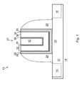
- FIG. 1illustrates an embodiment FinFET having a gate stack with an N work function metal layer including an oxidation layer on opposing sides of a tantalum aluminide carbide (TaAlC) layer;
- TaAlCtantalum aluminide carbide
- FIG. 2illustrates a line scan energy-dispersive x-ray spectrometry (EDS) graph for a representative slice of the gate stack of FIG. 1 ;
- EDSenergy-dispersive x-ray spectrometry
- FIG. 3illustrates a deposition system that may be utilized to form the N work function metal layer in the gate stack of the FinFET of FIG. 1 ;
- FIG. 4illustrates an embodiment method of forming N work function metal layer in the gate stack of the FinFET of FIG. 1 ;
- FIG. 5illustrates a repeating process of pulsing and purging to form monolayers of the tantalum aluminide carbide (TaAlC) layer in the N work function metal layer in the gate stack of the FinFET of FIG. 1 ;
- TaAlCtantalum aluminide carbide
- FIG. 6illustrates two reaction models illustrating the effect of temperature in forming the tantalum aluminide carbide (TaAlC) layer in the N work function metal layer in the gate stack of the FinFET of FIG. 1 ;
- FIG. 7is a chart illustrating the effect of temperature on a flat band voltage (V fb ) for a FinFET having an N work function metal layer formed from eleven monolayers;
- FIG. 8is a chart illustrating the effect of thickness of the N work function metal layer
- FIG. 9is a chart illustrating the effect of a precursor ratio on a flat band voltage (V fb ) for a FinFET having an N work function metal layer formed from eleven monolayers;
- FIG. 10is a chart depicting various parameters used for the aluminide carbide (TaAlC) layer composition.
- MOSmetal oxide semiconductor
- the embodiment FinFET 10includes a fin 12 formed from or on a semiconductor substrate 14 .
- the semiconductor substrate 14can be recessed to form the fin 12 .
- the fin 12can be epitaxially-grown on the semiconductor substrate 14 .
- the fin 12 and the semiconductor substrate 14are formed from silicon, germanium, silicon germanium, or another suitable semiconductor material.
- the fin 12extends between a source 16 and a drain 18 and defines a channel region 20 beneath a gate stack 22 .
- the gate stack 22is disposed over the channel region 20 of the fin 12 .
- spacers 24are supported by the fin 12 and disposed adjacent to the gate stack 22 .
- other integrated circuit structurese.g., contact plugs to the source 16 and the drain 18 , an interlevel dielectric (ILD) adjacent the spacers 24 , etc.
- ILDinterlevel dielectric
- the gate stack 22includes several layers.
- the gate stack 22includes a gate dielectric layer 26 .
- the gate dielectric layer 26is disposed over the fin 12 above the channel region 20 .
- the gate dielectric layer 26is disposed along sidewalls of the spacers 24 .
- the gate dielectric layer 26is formed from an interfacial dielectric and a high-k dielectric (IL/HK).
- the high-k dielectric portion of the gate dielectric layer 26has a thickness of about 15 Angstroms to about 25 Angstroms. Even so, in other embodiments the gate dielectric layer 26 and the high-k dielectric portion of the gate dielectric layer 26 may have other suitable thicknesses.
- a high-k dielectric cap layer 28is disposed over the gate dielectric layer 26 .
- the high-k dielectric cap layer 28may be formed from a suitable high-k dielectric material such as, for example, titanium nitride (TiN).
- TiNtitanium nitride
- the high-k dielectric cap layer 28has a thickness of between about 10 Angstroms and about 20 Angstroms. Even so, in other embodiments the high-k dielectric cap layer 28 may have other suitable thicknesses.
- a barrier/etch stop layer (ESL) 30is disposed over the high-k dielectric cap layer 28 .
- the barrier/etch stop layer 30may be formed from a suitable barrier or etch stop material such as, for example, tantalum nitride (TaN).
- the barrier/etch stop layer 30has a thickness of about 10 Angstroms to about 20 Angstroms. Even so, in other embodiments the barrier/etch stop layer 30 may have other suitable thicknesses.
- an N work function metal layer 32is disposed over the barrier/etch stop layer 30 .
- the N work function metal layer 32includes an oxidation layer 34 on opposing sides of a tantalum aluminide carbide (TaAlC) layer 36 .
- TaAlCtantalum aluminide carbide
- thin oxidation layers 34are observed on the surface of the tantalum aluminide carbide layer 36 at the interface of the barrier/etch stop layer 30 and the N work function metal layer 32 (e.g., TaAlC—TaN interface) and at the interface of a glue metal layer 38 and the N work function metal layer (e.g., TaAlC—TiN interface).
- the barrier/etch stop layer (ESL) 30engages with the oxidation layer 34 on an exterior side of the tantalum aluminide carbide layer 36 .
- the N work function metal layer 32includes about 16% to about 25% aluminum (Al), about 20% to about 29% carbon (C), about 7% to about 16% tantalum (Ta), and about 35% to about 50% oxygen (O).
- the ratio of Al/Cis about 0.5 to about 1.3
- the ratio of Ta/Cis about 0.2 to about 0.8
- the ratio of Al/Tais about 1 to about 3.6.
- a thickness of the N work function metal layer 32is between about 30 to about 90 Angstroms. Even so, in other embodiments the N work function metal layer 32 may have other suitable thicknesses.
- the tantalum aluminide carbide (TaAlC)which may be referred to as a metal carbide film, gives the FinFET 10 of FIG. 1 a tunable work function to meet device needs.
- the glue metal layer 38is disposed over the N work function metal layer 32 .
- the glue metal layer 38engages with the oxidation layer 34 on an interior side of the tantalum aluminide carbide layer 36 .
- the glue metal layer 38may be formed from a suitable glue material such as, for example, titanium nitride (TiN).
- TiNtitanium nitride
- the glue metal layer 38has a thickness of about 10 Angstroms to about 30 Angstroms. Even so, in other embodiments the glue metal layer 38 may have other suitable thicknesses.
- a metal fill layer 40is disposed over the glue metal layer 38 .
- the metal fill layer 40may be formed from a suitable metal such as, for example, tungsten (W).
- a line scan energy-dispersive x-ray spectrometry (EDS) graph 42is disposed over a representative slice 44 of the gate stack 22 of FIG. 1 .
- the oxidation layers 34 on opposing sides of the tantalum aluminide carbide (TaAlC) layer 36are aluminum (Al) and oxygen (O) rich.
- the deposition system 50may receive precursor materials from a first precursor delivery system 52 and a second precursor delivery system 54 .
- the formation of the N work function metal layer 32may be performed in a deposition chamber 56 that receives the first precursor material and the second precursor material.
- the first precursor delivery system 52 and the second precursor delivery system 54may work in conjunction with one another to supply the various different precursor materials to the deposition chamber 56 .
- the first precursor delivery system 52may include a carrier gas supply 58 , a flow controller 60 , and a precursor canister 62 .
- the carrier gas supply 58may supply a gas that may be used to help “carry” the precursor gas to the deposition chamber 56 .
- the carrier gasmay be an inert gas or other gas that does not react with the precursor material or other materials within the deposition system 50 .
- the carrier gasmay be argon (Ar), helium (He), nitrogen (N 2 ), hydrogen (H 2 ), combinations of these, and so on, although any other suitable carrier gas may alternatively be utilized.
- the carrier gas supply 58may be a vessel, such as a gas storage tank, that is located either locally to the deposition chamber 56 or else may be located remotely from the deposition chamber 56 .
- the carrier gas supply 58may supply the desired carrier gas to the flow controller 60 .
- the flow controller 60may be utilized to control the flow of the carrier gas to the precursor canister 62 and, eventually, to the deposition chamber 56 , thereby also helping to control the pressure within the deposition chamber 56 .
- the flow controller 60may be, for example, a proportional valve, a modulating valve, a needle valve, a pressure regulator, a mass flow controller, combinations of these, and so on.
- the flow controller 60may supply the controlled carrier gas to the precursor canister 62 .
- the precursor canister 62may be utilized to supply a desired precursor to the deposition chamber 56 by vaporizing or sublimating precursor materials that may be delivered in either a solid or liquid phase.
- the precursor canister 62may have a vapor region into which precursor material is driven into a gaseous phase so that the carrier gas from the flow controller 60 may enter the precursor canister 62 and pick-up or carry the gaseous precursor material out of the precursor canister 62 and towards the deposition chamber 56 .
- the second precursor delivery system 54may comprise components similar to the first precursor delivery system 52 . Indeed, the second precursor delivery system 54 may comprise a second precursor material supplier 64 , such as a gas storage tank or a machine to generate the second precursor material on an as-needed basis. The second precursor material supplier 64 may supply a stream of the second precursor material to, for example, a flow controller 60 similar to the flow controller described above with respect to the first precursor delivery system 52 .
- a second precursor material supplier 64such as a gas storage tank or a machine to generate the second precursor material on an as-needed basis.
- the second precursor material supplier 64may supply a stream of the second precursor material to, for example, a flow controller 60 similar to the flow controller described above with respect to the first precursor delivery system 52 .
- the flow controller 60 in the second precursor delivery system 54may help control the flow of the second precursor material to the precursor gas controller 66 , and may be, for example, a proportional valve, a modulating valve, a needle vale, a pressure regulator, a mass flow controller, a combination of these, or the like, although any other suitable method of controlling the flow of the second precursor material may alternatively be utilized.
- the second precursory delivery system 207may also include a precursor canister similar to precursor canister 62 of the first precursor delivery system 52 .
- the first precursor delivery system 52 and the second precursor delivery system 54may supply their individual precursor materials into a precursor gas controller 66 that connects and isolates the first precursor delivery system 52 and the second precursor delivery system 54 from the deposition chamber 56 in order to deliver the desired precursor material to the deposition chamber 56 .
- the precursor gas controller 66may include such devices as valves, flow meters, sensors, and the like to control the delivery rates of each of the precursors, and may be controlled by instructions received from a control unit 68 .
- the precursor gas controller 66upon receiving instructions from the control unit 68 , may open and close valves so as to connect one of the first precursor delivery system 52 and the second precursor delivery system 54 to the deposition chamber 56 . Such action directs a desired precursor material through a manifold 70 , into the deposition chamber 56 , and to a gas dispenser 72 , which could be a funnel or a showerhead (which are each shown in FIG. 3 ).
- the gas dispenser 72may be utilized to disperse the chosen precursor material into the deposition chamber 56 and may be designed to evenly disperse the precursor material in order to minimize undesired process conditions that may arise from uneven dispersal.
- the gas dispenser 72has a circular design with openings dispersed evenly to allow for the dispersal of the desired precursor material into the deposition chamber 56 .
- the deposition chamber 56may receive the desired precursor materials and expose the precursor materials to a wafer 74 having a plurality of FinFETs with a partially formed gate stack 22 thereon.
- the deposition chamber 56may be any desired shape that may be suitable for dispersing the precursor materials and contacting the precursor materials with the partially formed gate stack 22 .
- the deposition chamber 56has a cylindrical sidewall and corresponding circular bottom.
- the deposition chamber 56may be surrounded by a housing 76 made of material that is inert to the various process materials.
- the housing 76may be steel, stainless steel, nickel, aluminum, alloys of these, or combinations of these.
- the wafer 74may be placed on a pedestal 78 (or other mounting platform) in order to position and control the wafer 74 during the deposition process.
- the pedestal 221may include a heater 80 or other heating mechanism in order to heat the wafer 74 during the deposition process.
- the heater 80 in the pedestal 78is spaced apart from the gas dispenser 72 (i.e., the funnel or the showerhead) by about 50 mils to 150 mils. While a single pedestal 78 is illustrated in FIG. 3 , any number of pedestals 78 or mounting structures (with or without heaters) may additionally be included within the deposition chamber 56 .
- the deposition chamber 56may also have an exhaust outlet 82 for exhaust gases to exit the deposition chamber 56 .
- an argon (Ar) purge gasmay be removed from the deposition chamber 56 through the exhaust outlet 82 .
- a vacuum pump 84may be connected to the exhaust outlet 82 of the deposition chamber 56 in order to help evacuate the exhaust gases.
- the vacuum pump 84under control of the control unit 68 , may also be utilized to reduce and control the pressure within the deposition chamber 56 to a desired pressure. In an embodiment, the pressure within the deposition chamber 56 is maintained at about 2 Torr and about 5 Torr.
- the vacuum pump 84may also be utilized to evacuate one precursor material from the deposition chamber 56 in preparation for the introduction of the next precursor material.
- the deposition chamber 56may be purged of the precursor material therein.
- the control unit 68may instruct the precursor gas controller 66 to disconnect the first precursor delivery system 52 (containing the first precursor material to be purged from the deposition chamber 56 ) and to connect a purge gas delivery system 86 to deliver a purge gas to the deposition chamber 56 .
- the purge gas delivery system 86may be a gaseous tank or other facility that provides a purge gas such as argon (Ar), nitrogen (N 2 ), xenon (Xe), or other non-reactive gas to the deposition chamber 56 .
- the control unit 68may also initiate the vacuum pump 84 in order to apply a pressure differential to the deposition chamber 56 to aid in the removal of the first precursor material.
- the deposition system 50 of FIG. 3may be utilized to form the N work function metal layer 32 in the gate stack 22 of the FinFET 10 of FIG. 1 through an atomic layer deposition (ALD) process.
- ALDatomic layer deposition
- FIG. 4an embodiment method 90 of forming the gate stack 22 for the FinFET 10 is illustrated.
- the wafer 74(which has a plurality of FinFETs each with a partially formed gate stack 22 ) is loaded into the deposition chamber 56 .
- the wafer 74is heated using the heater 80 in the pedestal 78 .
- the wafer 74is heated to a temperature of between about 350 degrees Celsius to about 450 degrees Celsius.
- a first precursor of a tantalum pentachlorideis introduced or pulsed into the deposition chamber 56 .
- the first precursoris pulsed for between about 5 second to about 20 seconds. Even so, the first precursor may be pulsed for a longer or short time period.
- the first precursoris transported to the deposition chamber 56 using an argon (Ar) carrier gas with a flow rate of between about 500 standard cubic centimeters per minute (sccm) and about 1500 sccm.
- the first precursormay be pulsed at about 70 degrees Celsius to about 100 degrees Celsius. Even so, the first precursor may be pulsed with another suitable flow rate and another suitable temperature.
- the first precursor of the tantalum pentachloride (TaCl 5 )is purged from the atomic layer deposition chamber.
- the first precursoris purged for between about 2 second to about 10 seconds. Even so, the first precursor may be purged for a longer or short time period.
- the first precursoris purged from the deposition chamber 56 using an argon (Ar) purge gas with a flow rate of between about 2500 standard cubic centimeters per minute (sccm) and about 3500 sccm. Even so, the first precursor may be purged using another suitable gas with another suitable flow rate.
- a second precursor of triethylaluminum(Al(C 2 H 5 ) 3 ) is introduced or pulsed into the deposition chamber 56 .
- the second precursoris pulsed for between about 5 second to about 20 seconds. Even so, the second precursor may be pulsed for a longer or short time period.
- the second precursoris transported to the deposition chamber 56 using an argon (Ar) carrier gas with a flow rate of between about 500 standard cubic centimeters per minute (sccm) and about 1500 sccm.
- the second precursormay be pulsed at about 25 degrees Celsius to about 45 degrees Celsius. Even so, the second precursor may be pulsed with another suitable flow rate and another suitable temperature.
- the second precursor of the triethylaluminum(Al(C 2 H 5 ) 3 ) is purged from the deposition chamber 56 .
- the second precursoris purged for between about 2 second to about 10 seconds. Even so, the second precursor may be purged for a longer or short time period.
- the first precursoris purged from the deposition chamber 56 using an argon (Ar) purge gas with a flow rate of between about 2500 standard cubic centimeters per minute (sccm) and about 3500 sccm. Even so, the second precursor may be purged using another suitable gas with another suitable flow rate.
- the N work function metal layer 32 for the gate stack 22is generated after a suitable opportunity for oxidation.
- the N work function metal layer 32has oxidation layers 24 on opposing sides of the tantalum aluminide carbide (TaAlC) layer 36 .
- the process 104 of pulsing the first precursor 106 , purging the first precursor 108 , pulsing the second precursor 110 , and then purging the second precursor 112may be repeated to form additional monolayers of the tantalum aluminide carbide (TaAlC) layer 36 .
- TaAlCtantalum aluminide carbide
- the tantalum aluminide carbide (TaAlC) layer 36may be exposed to oxygen to permit oxidation to occur.
- TaC and TaAlCare formed in the reaction.
- TaAlCtantalum aluminide carbide
- a chart 116 illustrating the effect of temperature on a flat band voltage (V fb ) for a MOS capacitor having an N work function metal layer formed from eleven monolayersis provided.
- the flat band voltagechanges from about ⁇ 0.17 V to about ⁇ 0.39 V as the temperature is increased from about 350° C. to about 400° C.
- the N work function metal layerincludes tantalum aluminide carbide (TaAlC) and a metal fill layer of tungsten (W) is used.
- the chart 116also includes the flat band voltage for a FinFET with the N work function metal layer of tantalum aluminide carbide (TaAlC) and a metal fill layer of aluminum (Al), which is labeled as N 14 in the chart 116 .
- TaAlCtantalum aluminide carbide
- Alaluminum
- a chart 118 illustrating the effect of thickness of the N work function metal layeris provided.
- the flat band voltagechanges from about ⁇ 0.25 V to about ⁇ 0.38 V as the thickness of the N work function metal layer changes from 9 monolayers (9 ⁇ ) to about 15 monolayers (15 ⁇ ).
- the comparison of the flat band voltages at various thicknessesis made with a process temperature of about 400° C.
- a chart 120 illustrating the effect of a precursor ratio on a flat band voltage (V fb ) for a FinFET having an N work function metal layer formed from eleven monolayersis provided.
- the flat band voltagehas a range of about ⁇ 0.32 V to about ⁇ 0.37 V when the ratio of tantalum pentachloride (TaCl 5 ) to triethylaluminum (Al(C 2 H 5 ) 3 ) used to form the aluminide carbide (TaAlC) layer of the N work function metal layer 32 is about 15 to 7.
- the flat band voltagehas a range of about ⁇ 0.35 V to about ⁇ 0.40 V when the ratio of tantalum pentachloride (TaCl 5 ) to triethylaluminum (Al(C 2 H 5 ) 3 ) is about 10 to 10.
- the flat band voltagehas a range of about ⁇ 0.37 V to about ⁇ 0.43 V when the ratio of tantalum pentachloride (TaCl 5 ) to triethylaluminum (Al(C 2 H 5 ) 3 ) is about 7 to 15.
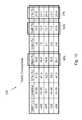
- a chart 122 depicting various parameters used for the tantalum aluminide carbide (TaAlC) layer 36 compositionis provided. As shown, the chart includes temperature ranges, precursor ratios (labeled as the “condition”), the percentage of oxygen, the percentage of aluminum, the percentage of chlorine, the percentage of tantalum, and the percentage of carbon. For reference, the percentages of aluminum, tantalum, and carbon have been highlighted.
- An embodiment fin field effect transistorincluding a fin supported by a semiconductor substrate, the fin extending between a source and a drain and having a channel region, and a gate stack formed over the channel region of the fin, the gate stack including an N work function metal layer comprising an oxidation layer on opposing sides of a tantalum aluminide carbide (TaAlC) layer.
- FinFETfin field effect transistor
- An embodiment method of forming a gate stack for a fin field effect transistorincluding heating a wafer having the FinFET in an atomic layer deposition chamber, pulsing a first precursor of a tantalum pentachloride (TaCl 5 ) into the atomic layer deposition chamber with the wafer having the FinFET, purging the first precursor of the tantalum pentachloride (TaCl 5 ) from the atomic layer deposition chamber, pulsing a second precursor of triethylaluminum (Al(C 2 H 5 ) 3 ) into the atomic layer deposition chamber with the wafer having the FinFET, and purging the second precursor of the triethylaluminum (Al(C 2 H 5 ) 3 ) from the atomic layer deposition chamber with the wafer having the FinFET to generate an N work function metal layer for the gate stack, the N work function metal layer comprising a tantalum aluminide carbide (TaAlC) layer
- An embodiment N metal work function composition for a gate stack of a fin field effect transistor (FinFET)including aluminum in a range of between about 16% to about 25%, carbon in a range of between about 20% to about 29%, tantalum in a range of between about 9% to about 16%, and oxygen in a range of between about 35% to about 50%.
- FinFETfin field effect transistor
Landscapes
- Engineering & Computer Science (AREA)
- Physics & Mathematics (AREA)
- Condensed Matter Physics & Semiconductors (AREA)
- General Physics & Mathematics (AREA)
- Manufacturing & Machinery (AREA)
- Computer Hardware Design (AREA)
- Microelectronics & Electronic Packaging (AREA)
- Power Engineering (AREA)
- Chemical & Material Sciences (AREA)
- Composite Materials (AREA)
- Chemical Kinetics & Catalysis (AREA)
- Crystallography & Structural Chemistry (AREA)
- General Chemical & Material Sciences (AREA)
- Insulated Gate Type Field-Effect Transistor (AREA)
- Materials Engineering (AREA)
- Semiconductor Memories (AREA)
- Electrodes Of Semiconductors (AREA)
- Formation Of Insulating Films (AREA)
Abstract
Description
Claims (20)
Priority Applications (4)
| Application Number | Priority Date | Filing Date | Title |
|---|---|---|---|
| US13/720,732US9064857B2 (en) | 2012-12-19 | 2012-12-19 | N metal for FinFET |
| KR1020130020546AKR101552005B1 (en) | 2012-12-19 | 2013-02-26 | N metal for finfet |
| CN201310072572.6ACN103887340B (en) | 2012-12-19 | 2013-03-07 | N workfunction layers for FinFET |
| US14/669,786US9293334B2 (en) | 2012-12-19 | 2015-03-26 | N metal for FinFET and methods of forming |
Applications Claiming Priority (1)
| Application Number | Priority Date | Filing Date | Title |
|---|---|---|---|
| US13/720,732US9064857B2 (en) | 2012-12-19 | 2012-12-19 | N metal for FinFET |
Related Child Applications (1)
| Application Number | Title | Priority Date | Filing Date |
|---|---|---|---|
| US14/669,786DivisionUS9293334B2 (en) | 2012-12-19 | 2015-03-26 | N metal for FinFET and methods of forming |
Publications (2)
| Publication Number | Publication Date |
|---|---|
| US20140167187A1 US20140167187A1 (en) | 2014-06-19 |
| US9064857B2true US9064857B2 (en) | 2015-06-23 |
Family
ID=50929949
Family Applications (2)
| Application Number | Title | Priority Date | Filing Date |
|---|---|---|---|
| US13/720,732Expired - Fee RelatedUS9064857B2 (en) | 2012-12-19 | 2012-12-19 | N metal for FinFET |
| US14/669,786ActiveUS9293334B2 (en) | 2012-12-19 | 2015-03-26 | N metal for FinFET and methods of forming |
Family Applications After (1)
| Application Number | Title | Priority Date | Filing Date |
|---|---|---|---|
| US14/669,786ActiveUS9293334B2 (en) | 2012-12-19 | 2015-03-26 | N metal for FinFET and methods of forming |
Country Status (3)
| Country | Link |
|---|---|
| US (2) | US9064857B2 (en) |
| KR (1) | KR101552005B1 (en) |
| CN (1) | CN103887340B (en) |
Cited By (3)
| Publication number | Priority date | Publication date | Assignee | Title |
|---|---|---|---|---|
| US20180240884A1 (en)* | 2015-06-10 | 2018-08-23 | International Business Machines Corporation | Spacer chamfering gate stack scheme |
| US10950431B2 (en) | 2017-09-29 | 2021-03-16 | Taiwan Semiconductor Manufacturing Co. Ltd. | Low-k feature formation processes and structures formed thereby |
| US11295948B2 (en) | 2017-09-29 | 2022-04-05 | Taiwan Semiconductor Manufacturing Co., Ltd. | Low-K feature formation processes and structures formed thereby |
Families Citing this family (362)
| Publication number | Priority date | Publication date | Assignee | Title |
|---|---|---|---|---|
| US10378106B2 (en) | 2008-11-14 | 2019-08-13 | Asm Ip Holding B.V. | Method of forming insulation film by modified PEALD |
| US9394608B2 (en) | 2009-04-06 | 2016-07-19 | Asm America, Inc. | Semiconductor processing reactor and components thereof |
| US8802201B2 (en) | 2009-08-14 | 2014-08-12 | Asm America, Inc. | Systems and methods for thin-film deposition of metal oxides using excited nitrogen-oxygen species |
| US9312155B2 (en) | 2011-06-06 | 2016-04-12 | Asm Japan K.K. | High-throughput semiconductor-processing apparatus equipped with multiple dual-chamber modules |
| US10364496B2 (en) | 2011-06-27 | 2019-07-30 | Asm Ip Holding B.V. | Dual section module having shared and unshared mass flow controllers |
| US10854498B2 (en) | 2011-07-15 | 2020-12-01 | Asm Ip Holding B.V. | Wafer-supporting device and method for producing same |
| US20130023129A1 (en) | 2011-07-20 | 2013-01-24 | Asm America, Inc. | Pressure transmitter for a semiconductor processing environment |
| US9017481B1 (en) | 2011-10-28 | 2015-04-28 | Asm America, Inc. | Process feed management for semiconductor substrate processing |
| US9659799B2 (en) | 2012-08-28 | 2017-05-23 | Asm Ip Holding B.V. | Systems and methods for dynamic semiconductor process scheduling |
| US10714315B2 (en) | 2012-10-12 | 2020-07-14 | Asm Ip Holdings B.V. | Semiconductor reaction chamber showerhead |
| US20160376700A1 (en) | 2013-02-01 | 2016-12-29 | Asm Ip Holding B.V. | System for treatment of deposition reactor |
| US9484191B2 (en) | 2013-03-08 | 2016-11-01 | Asm Ip Holding B.V. | Pulsed remote plasma method and system |
| US9589770B2 (en) | 2013-03-08 | 2017-03-07 | Asm Ip Holding B.V. | Method and systems for in-situ formation of intermediate reactive species |
| KR20140121634A (en)* | 2013-04-08 | 2014-10-16 | 삼성전자주식회사 | Semiconductor device and fabricating method thereof |
| US9240412B2 (en) | 2013-09-27 | 2016-01-19 | Asm Ip Holding B.V. | Semiconductor structure and device and methods of forming same using selective epitaxial process |
| US10683571B2 (en) | 2014-02-25 | 2020-06-16 | Asm Ip Holding B.V. | Gas supply manifold and method of supplying gases to chamber using same |
| US10167557B2 (en) | 2014-03-18 | 2019-01-01 | Asm Ip Holding B.V. | Gas distribution system, reactor including the system, and methods of using the same |
| US11015245B2 (en) | 2014-03-19 | 2021-05-25 | Asm Ip Holding B.V. | Gas-phase reactor and system having exhaust plenum and components thereof |
| US10858737B2 (en) | 2014-07-28 | 2020-12-08 | Asm Ip Holding B.V. | Showerhead assembly and components thereof |
| US9890456B2 (en) | 2014-08-21 | 2018-02-13 | Asm Ip Holding B.V. | Method and system for in situ formation of gas-phase compounds |
| US9657845B2 (en) | 2014-10-07 | 2017-05-23 | Asm Ip Holding B.V. | Variable conductance gas distribution apparatus and method |
| US10941490B2 (en) | 2014-10-07 | 2021-03-09 | Asm Ip Holding B.V. | Multiple temperature range susceptor, assembly, reactor and system including the susceptor, and methods of using the same |
| US10134861B2 (en) | 2014-10-08 | 2018-11-20 | Taiwan Semiconductor Manufacturing Co., Ltd. | Semiconductor device structure and method for forming the same |
| KR102263121B1 (en) | 2014-12-22 | 2021-06-09 | 에이에스엠 아이피 홀딩 비.브이. | Semiconductor device and manufacuring method thereof |
| CN105826372B (en)* | 2015-01-06 | 2018-12-21 | 中芯国际集成电路制造(上海)有限公司 | FinFET and forming method thereof |
| US10529542B2 (en) | 2015-03-11 | 2020-01-07 | Asm Ip Holdings B.V. | Cross-flow reactor and method |
| US10276355B2 (en) | 2015-03-12 | 2019-04-30 | Asm Ip Holding B.V. | Multi-zone reactor, system including the reactor, and method of using the same |
| CN106298663B (en)* | 2015-05-22 | 2019-04-09 | 中芯国际集成电路制造(上海)有限公司 | A kind of semiconductor device and its manufacturing method, electronic device |
| US10458018B2 (en) | 2015-06-26 | 2019-10-29 | Asm Ip Holding B.V. | Structures including metal carbide material, devices including the structures, and methods of forming same |
| US10600673B2 (en) | 2015-07-07 | 2020-03-24 | Asm Ip Holding B.V. | Magnetic susceptor to baseplate seal |
| US9960072B2 (en) | 2015-09-29 | 2018-05-01 | Asm Ip Holding B.V. | Variable adjustment for precise matching of multiple chamber cavity housings |
| US10211308B2 (en) | 2015-10-21 | 2019-02-19 | Asm Ip Holding B.V. | NbMC layers |
| US9824929B2 (en) | 2015-10-28 | 2017-11-21 | Taiwan Semiconductor Manufacturing Co., Ltd. | FinFET gate structure and method for fabricating the same |
| US9620610B1 (en)* | 2015-10-28 | 2017-04-11 | Taiwan Semiconductor Manufacturing Co., Ltd. | FinFET gate structure and method for fabricating the same |
| US10322384B2 (en) | 2015-11-09 | 2019-06-18 | Asm Ip Holding B.V. | Counter flow mixer for process chamber |
| US11139308B2 (en) | 2015-12-29 | 2021-10-05 | Asm Ip Holding B.V. | Atomic layer deposition of III-V compounds to form V-NAND devices |
| US10468251B2 (en) | 2016-02-19 | 2019-11-05 | Asm Ip Holding B.V. | Method for forming spacers using silicon nitride film for spacer-defined multiple patterning |
| US10529554B2 (en) | 2016-02-19 | 2020-01-07 | Asm Ip Holding B.V. | Method for forming silicon nitride film selectively on sidewalls or flat surfaces of trenches |
| US10501866B2 (en) | 2016-03-09 | 2019-12-10 | Asm Ip Holding B.V. | Gas distribution apparatus for improved film uniformity in an epitaxial system |
| US10343920B2 (en) | 2016-03-18 | 2019-07-09 | Asm Ip Holding B.V. | Aligned carbon nanotubes |
| US9892913B2 (en) | 2016-03-24 | 2018-02-13 | Asm Ip Holding B.V. | Radial and thickness control via biased multi-port injection settings |
| US10865475B2 (en) | 2016-04-21 | 2020-12-15 | Asm Ip Holding B.V. | Deposition of metal borides and silicides |
| US10190213B2 (en) | 2016-04-21 | 2019-01-29 | Asm Ip Holding B.V. | Deposition of metal borides |
| US10367080B2 (en) | 2016-05-02 | 2019-07-30 | Asm Ip Holding B.V. | Method of forming a germanium oxynitride film |
| US10032628B2 (en) | 2016-05-02 | 2018-07-24 | Asm Ip Holding B.V. | Source/drain performance through conformal solid state doping |
| KR102592471B1 (en) | 2016-05-17 | 2023-10-20 | 에이에스엠 아이피 홀딩 비.브이. | Method of forming metal interconnection and method of fabricating semiconductor device using the same |
| US11453943B2 (en) | 2016-05-25 | 2022-09-27 | Asm Ip Holding B.V. | Method for forming carbon-containing silicon/metal oxide or nitride film by ALD using silicon precursor and hydrocarbon precursor |
| US10388509B2 (en) | 2016-06-28 | 2019-08-20 | Asm Ip Holding B.V. | Formation of epitaxial layers via dislocation filtering |
| US10612137B2 (en) | 2016-07-08 | 2020-04-07 | Asm Ip Holdings B.V. | Organic reactants for atomic layer deposition |
| US9859151B1 (en) | 2016-07-08 | 2018-01-02 | Asm Ip Holding B.V. | Selective film deposition method to form air gaps |
| US10714385B2 (en) | 2016-07-19 | 2020-07-14 | Asm Ip Holding B.V. | Selective deposition of tungsten |
| KR102354490B1 (en) | 2016-07-27 | 2022-01-21 | 에이에스엠 아이피 홀딩 비.브이. | Method of processing a substrate |
| US9887082B1 (en) | 2016-07-28 | 2018-02-06 | Asm Ip Holding B.V. | Method and apparatus for filling a gap |
| US9812320B1 (en) | 2016-07-28 | 2017-11-07 | Asm Ip Holding B.V. | Method and apparatus for filling a gap |
| KR102532607B1 (en) | 2016-07-28 | 2023-05-15 | 에이에스엠 아이피 홀딩 비.브이. | Substrate processing apparatus and method of operating the same |
| US10395919B2 (en) | 2016-07-28 | 2019-08-27 | Asm Ip Holding B.V. | Method and apparatus for filling a gap |
| KR102613349B1 (en) | 2016-08-25 | 2023-12-14 | 에이에스엠 아이피 홀딩 비.브이. | Exhaust apparatus and substrate processing apparatus and thin film fabricating method using the same |
| US10410943B2 (en) | 2016-10-13 | 2019-09-10 | Asm Ip Holding B.V. | Method for passivating a surface of a semiconductor and related systems |
| US10643826B2 (en) | 2016-10-26 | 2020-05-05 | Asm Ip Holdings B.V. | Methods for thermally calibrating reaction chambers |
| US11532757B2 (en) | 2016-10-27 | 2022-12-20 | Asm Ip Holding B.V. | Deposition of charge trapping layers |
| US10229833B2 (en) | 2016-11-01 | 2019-03-12 | Asm Ip Holding B.V. | Methods for forming a transition metal nitride film on a substrate by atomic layer deposition and related semiconductor device structures |
| US10435790B2 (en) | 2016-11-01 | 2019-10-08 | Asm Ip Holding B.V. | Method of subatmospheric plasma-enhanced ALD using capacitively coupled electrodes with narrow gap |
| US10714350B2 (en) | 2016-11-01 | 2020-07-14 | ASM IP Holdings, B.V. | Methods for forming a transition metal niobium nitride film on a substrate by atomic layer deposition and related semiconductor device structures |
| US10643904B2 (en) | 2016-11-01 | 2020-05-05 | Asm Ip Holdings B.V. | Methods for forming a semiconductor device and related semiconductor device structures |
| US10134757B2 (en) | 2016-11-07 | 2018-11-20 | Asm Ip Holding B.V. | Method of processing a substrate and a device manufactured by using the method |
| KR102546317B1 (en) | 2016-11-15 | 2023-06-21 | 에이에스엠 아이피 홀딩 비.브이. | Gas supply unit and substrate processing apparatus including the same |
| US10340135B2 (en) | 2016-11-28 | 2019-07-02 | Asm Ip Holding B.V. | Method of topologically restricted plasma-enhanced cyclic deposition of silicon or metal nitride |
| KR102762543B1 (en) | 2016-12-14 | 2025-02-05 | 에이에스엠 아이피 홀딩 비.브이. | Substrate processing apparatus |
| US11447861B2 (en) | 2016-12-15 | 2022-09-20 | Asm Ip Holding B.V. | Sequential infiltration synthesis apparatus and a method of forming a patterned structure |
| US11581186B2 (en) | 2016-12-15 | 2023-02-14 | Asm Ip Holding B.V. | Sequential infiltration synthesis apparatus |
| KR102700194B1 (en) | 2016-12-19 | 2024-08-28 | 에이에스엠 아이피 홀딩 비.브이. | Substrate processing apparatus |
| US10269558B2 (en) | 2016-12-22 | 2019-04-23 | Asm Ip Holding B.V. | Method of forming a structure on a substrate |
| US10867788B2 (en) | 2016-12-28 | 2020-12-15 | Asm Ip Holding B.V. | Method of forming a structure on a substrate |
| US11390950B2 (en) | 2017-01-10 | 2022-07-19 | Asm Ip Holding B.V. | Reactor system and method to reduce residue buildup during a film deposition process |
| US10655221B2 (en) | 2017-02-09 | 2020-05-19 | Asm Ip Holding B.V. | Method for depositing oxide film by thermal ALD and PEALD |
| US10468261B2 (en) | 2017-02-15 | 2019-11-05 | Asm Ip Holding B.V. | Methods for forming a metallic film on a substrate by cyclical deposition and related semiconductor device structures |
| US10283353B2 (en) | 2017-03-29 | 2019-05-07 | Asm Ip Holding B.V. | Method of reforming insulating film deposited on substrate with recess pattern |
| US10529563B2 (en) | 2017-03-29 | 2020-01-07 | Asm Ip Holdings B.V. | Method for forming doped metal oxide films on a substrate by cyclical deposition and related semiconductor device structures |
| US10319826B2 (en)* | 2017-04-12 | 2019-06-11 | International Business Machines Corporation | Replacement metal gate stack with oxygen and nitrogen scavenging layers |
| KR102457289B1 (en) | 2017-04-25 | 2022-10-21 | 에이에스엠 아이피 홀딩 비.브이. | Method for depositing a thin film and manufacturing a semiconductor device |
| US10446393B2 (en) | 2017-05-08 | 2019-10-15 | Asm Ip Holding B.V. | Methods for forming silicon-containing epitaxial layers and related semiconductor device structures |
| US10770286B2 (en) | 2017-05-08 | 2020-09-08 | Asm Ip Holdings B.V. | Methods for selectively forming a silicon nitride film on a substrate and related semiconductor device structures |
| US10892156B2 (en) | 2017-05-08 | 2021-01-12 | Asm Ip Holding B.V. | Methods for forming a silicon nitride film on a substrate and related semiconductor device structures |
| US10504742B2 (en) | 2017-05-31 | 2019-12-10 | Asm Ip Holding B.V. | Method of atomic layer etching using hydrogen plasma |
| US10886123B2 (en) | 2017-06-02 | 2021-01-05 | Asm Ip Holding B.V. | Methods for forming low temperature semiconductor layers and related semiconductor device structures |
| US12040200B2 (en) | 2017-06-20 | 2024-07-16 | Asm Ip Holding B.V. | Semiconductor processing apparatus and methods for calibrating a semiconductor processing apparatus |
| US11306395B2 (en) | 2017-06-28 | 2022-04-19 | Asm Ip Holding B.V. | Methods for depositing a transition metal nitride film on a substrate by atomic layer deposition and related deposition apparatus |
| US10685834B2 (en) | 2017-07-05 | 2020-06-16 | Asm Ip Holdings B.V. | Methods for forming a silicon germanium tin layer and related semiconductor device structures |
| KR20190009245A (en) | 2017-07-18 | 2019-01-28 | 에이에스엠 아이피 홀딩 비.브이. | Methods for forming a semiconductor device structure and related semiconductor device structures |
| US11374112B2 (en) | 2017-07-19 | 2022-06-28 | Asm Ip Holding B.V. | Method for depositing a group IV semiconductor and related semiconductor device structures |
| US10541333B2 (en) | 2017-07-19 | 2020-01-21 | Asm Ip Holding B.V. | Method for depositing a group IV semiconductor and related semiconductor device structures |
| US11018002B2 (en) | 2017-07-19 | 2021-05-25 | Asm Ip Holding B.V. | Method for selectively depositing a Group IV semiconductor and related semiconductor device structures |
| US10590535B2 (en) | 2017-07-26 | 2020-03-17 | Asm Ip Holdings B.V. | Chemical treatment, deposition and/or infiltration apparatus and method for using the same |
| US10605530B2 (en) | 2017-07-26 | 2020-03-31 | Asm Ip Holding B.V. | Assembly of a liner and a flange for a vertical furnace as well as the liner and the vertical furnace |
| US10312055B2 (en) | 2017-07-26 | 2019-06-04 | Asm Ip Holding B.V. | Method of depositing film by PEALD using negative bias |
| TWI815813B (en) | 2017-08-04 | 2023-09-21 | 荷蘭商Asm智慧財產控股公司 | Showerhead assembly for distributing a gas within a reaction chamber |
| US10692741B2 (en) | 2017-08-08 | 2020-06-23 | Asm Ip Holdings B.V. | Radiation shield |
| US10770336B2 (en) | 2017-08-08 | 2020-09-08 | Asm Ip Holding B.V. | Substrate lift mechanism and reactor including same |
| US11769682B2 (en) | 2017-08-09 | 2023-09-26 | Asm Ip Holding B.V. | Storage apparatus for storing cassettes for substrates and processing apparatus equipped therewith |
| US10249524B2 (en) | 2017-08-09 | 2019-04-02 | Asm Ip Holding B.V. | Cassette holder assembly for a substrate cassette and holding member for use in such assembly |
| US11139191B2 (en) | 2017-08-09 | 2021-10-05 | Asm Ip Holding B.V. | Storage apparatus for storing cassettes for substrates and processing apparatus equipped therewith |
| USD900036S1 (en) | 2017-08-24 | 2020-10-27 | Asm Ip Holding B.V. | Heater electrical connector and adapter |
| US11830730B2 (en) | 2017-08-29 | 2023-11-28 | Asm Ip Holding B.V. | Layer forming method and apparatus |
| KR102491945B1 (en) | 2017-08-30 | 2023-01-26 | 에이에스엠 아이피 홀딩 비.브이. | Substrate processing apparatus |
| US11056344B2 (en) | 2017-08-30 | 2021-07-06 | Asm Ip Holding B.V. | Layer forming method |
| US11295980B2 (en) | 2017-08-30 | 2022-04-05 | Asm Ip Holding B.V. | Methods for depositing a molybdenum metal film over a dielectric surface of a substrate by a cyclical deposition process and related semiconductor device structures |
| KR102401446B1 (en) | 2017-08-31 | 2022-05-24 | 에이에스엠 아이피 홀딩 비.브이. | Substrate processing apparatus |
| KR102379707B1 (en) | 2017-09-13 | 2022-03-28 | 삼성전자주식회사 | semiconductor device |
| US10607895B2 (en) | 2017-09-18 | 2020-03-31 | Asm Ip Holdings B.V. | Method for forming a semiconductor device structure comprising a gate fill metal |
| KR102630301B1 (en) | 2017-09-21 | 2024-01-29 | 에이에스엠 아이피 홀딩 비.브이. | Method of sequential infiltration synthesis treatment of infiltrateable material and structures and devices formed using same |
| US10844484B2 (en) | 2017-09-22 | 2020-11-24 | Asm Ip Holding B.V. | Apparatus for dispensing a vapor phase reactant to a reaction chamber and related methods |
| US10658205B2 (en) | 2017-09-28 | 2020-05-19 | Asm Ip Holdings B.V. | Chemical dispensing apparatus and methods for dispensing a chemical to a reaction chamber |
| US10403504B2 (en) | 2017-10-05 | 2019-09-03 | Asm Ip Holding B.V. | Method for selectively depositing a metallic film on a substrate |
| US10319588B2 (en) | 2017-10-10 | 2019-06-11 | Asm Ip Holding B.V. | Method for depositing a metal chalcogenide on a substrate by cyclical deposition |
| US10923344B2 (en) | 2017-10-30 | 2021-02-16 | Asm Ip Holding B.V. | Methods for forming a semiconductor structure and related semiconductor structures |
| US10529815B2 (en)* | 2017-10-31 | 2020-01-07 | International Business Machines Corporation | Conformal replacement gate electrode for short channel devices |
| US10910262B2 (en) | 2017-11-16 | 2021-02-02 | Asm Ip Holding B.V. | Method of selectively depositing a capping layer structure on a semiconductor device structure |
| KR102443047B1 (en) | 2017-11-16 | 2022-09-14 | 에이에스엠 아이피 홀딩 비.브이. | Method of processing a substrate and a device manufactured by the same |
| US11022879B2 (en) | 2017-11-24 | 2021-06-01 | Asm Ip Holding B.V. | Method of forming an enhanced unexposed photoresist layer |
| WO2019103613A1 (en) | 2017-11-27 | 2019-05-31 | Asm Ip Holding B.V. | A storage device for storing wafer cassettes for use with a batch furnace |
| CN111344522B (en) | 2017-11-27 | 2022-04-12 | 阿斯莫Ip控股公司 | Including clean mini-environment device |
| US10290508B1 (en) | 2017-12-05 | 2019-05-14 | Asm Ip Holding B.V. | Method for forming vertical spacers for spacer-defined patterning |
| US10872771B2 (en) | 2018-01-16 | 2020-12-22 | Asm Ip Holding B. V. | Method for depositing a material film on a substrate within a reaction chamber by a cyclical deposition process and related device structures |
| KR102695659B1 (en) | 2018-01-19 | 2024-08-14 | 에이에스엠 아이피 홀딩 비.브이. | Method for depositing a gap filling layer by plasma assisted deposition |
| TWI799494B (en) | 2018-01-19 | 2023-04-21 | 荷蘭商Asm 智慧財產控股公司 | Deposition method |
| USD903477S1 (en) | 2018-01-24 | 2020-12-01 | Asm Ip Holdings B.V. | Metal clamp |
| US11018047B2 (en) | 2018-01-25 | 2021-05-25 | Asm Ip Holding B.V. | Hybrid lift pin |
| US10535516B2 (en) | 2018-02-01 | 2020-01-14 | Asm Ip Holdings B.V. | Method for depositing a semiconductor structure on a surface of a substrate and related semiconductor structures |
| USD880437S1 (en) | 2018-02-01 | 2020-04-07 | Asm Ip Holding B.V. | Gas supply plate for semiconductor manufacturing apparatus |
| US11081345B2 (en) | 2018-02-06 | 2021-08-03 | Asm Ip Holding B.V. | Method of post-deposition treatment for silicon oxide film |
| US10896820B2 (en) | 2018-02-14 | 2021-01-19 | Asm Ip Holding B.V. | Method for depositing a ruthenium-containing film on a substrate by a cyclical deposition process |
| WO2019158960A1 (en) | 2018-02-14 | 2019-08-22 | Asm Ip Holding B.V. | A method for depositing a ruthenium-containing film on a substrate by a cyclical deposition process |
| US10731249B2 (en) | 2018-02-15 | 2020-08-04 | Asm Ip Holding B.V. | Method of forming a transition metal containing film on a substrate by a cyclical deposition process, a method for supplying a transition metal halide compound to a reaction chamber, and related vapor deposition apparatus |
| US10658181B2 (en) | 2018-02-20 | 2020-05-19 | Asm Ip Holding B.V. | Method of spacer-defined direct patterning in semiconductor fabrication |
| KR102636427B1 (en) | 2018-02-20 | 2024-02-13 | 에이에스엠 아이피 홀딩 비.브이. | Substrate processing method and apparatus |
| US10975470B2 (en) | 2018-02-23 | 2021-04-13 | Asm Ip Holding B.V. | Apparatus for detecting or monitoring for a chemical precursor in a high temperature environment |
| US11473195B2 (en) | 2018-03-01 | 2022-10-18 | Asm Ip Holding B.V. | Semiconductor processing apparatus and a method for processing a substrate |
| US11629406B2 (en) | 2018-03-09 | 2023-04-18 | Asm Ip Holding B.V. | Semiconductor processing apparatus comprising one or more pyrometers for measuring a temperature of a substrate during transfer of the substrate |
| US11114283B2 (en) | 2018-03-16 | 2021-09-07 | Asm Ip Holding B.V. | Reactor, system including the reactor, and methods of manufacturing and using same |
| KR102646467B1 (en) | 2018-03-27 | 2024-03-11 | 에이에스엠 아이피 홀딩 비.브이. | Method of forming an electrode on a substrate and a semiconductor device structure including an electrode |
| US10510536B2 (en) | 2018-03-29 | 2019-12-17 | Asm Ip Holding B.V. | Method of depositing a co-doped polysilicon film on a surface of a substrate within a reaction chamber |
| US11230766B2 (en) | 2018-03-29 | 2022-01-25 | Asm Ip Holding B.V. | Substrate processing apparatus and method |
| US11088002B2 (en) | 2018-03-29 | 2021-08-10 | Asm Ip Holding B.V. | Substrate rack and a substrate processing system and method |
| KR102501472B1 (en) | 2018-03-30 | 2023-02-20 | 에이에스엠 아이피 홀딩 비.브이. | Substrate processing method |
| KR102600229B1 (en) | 2018-04-09 | 2023-11-10 | 에이에스엠 아이피 홀딩 비.브이. | Substrate supporting device, substrate processing apparatus including the same and substrate processing method |
| TWI811348B (en) | 2018-05-08 | 2023-08-11 | 荷蘭商Asm 智慧財產控股公司 | Methods for depositing an oxide film on a substrate by a cyclical deposition process and related device structures |
| US12025484B2 (en) | 2018-05-08 | 2024-07-02 | Asm Ip Holding B.V. | Thin film forming method |
| US12272527B2 (en) | 2018-05-09 | 2025-04-08 | Asm Ip Holding B.V. | Apparatus for use with hydrogen radicals and method of using same |
| KR20190129718A (en) | 2018-05-11 | 2019-11-20 | 에이에스엠 아이피 홀딩 비.브이. | Methods for forming a doped metal carbide film on a substrate and related semiconductor device structures |
| KR102596988B1 (en) | 2018-05-28 | 2023-10-31 | 에이에스엠 아이피 홀딩 비.브이. | Method of processing a substrate and a device manufactured by the same |
| US11718913B2 (en) | 2018-06-04 | 2023-08-08 | Asm Ip Holding B.V. | Gas distribution system and reactor system including same |
| TWI840362B (en) | 2018-06-04 | 2024-05-01 | 荷蘭商Asm Ip私人控股有限公司 | Wafer handling chamber with moisture reduction |
| US11286562B2 (en) | 2018-06-08 | 2022-03-29 | Asm Ip Holding B.V. | Gas-phase chemical reactor and method of using same |
| KR102568797B1 (en) | 2018-06-21 | 2023-08-21 | 에이에스엠 아이피 홀딩 비.브이. | Substrate processing system |
| US10797133B2 (en) | 2018-06-21 | 2020-10-06 | Asm Ip Holding B.V. | Method for depositing a phosphorus doped silicon arsenide film and related semiconductor device structures |
| KR102854019B1 (en) | 2018-06-27 | 2025-09-02 | 에이에스엠 아이피 홀딩 비.브이. | Periodic deposition method for forming a metal-containing material and films and structures comprising the metal-containing material |
| TWI873894B (en) | 2018-06-27 | 2025-02-21 | 荷蘭商Asm Ip私人控股有限公司 | Cyclic deposition methods for forming metal-containing material and films and structures including the metal-containing material |
| KR102686758B1 (en) | 2018-06-29 | 2024-07-18 | 에이에스엠 아이피 홀딩 비.브이. | Method for depositing a thin film and manufacturing a semiconductor device |
| US10612136B2 (en) | 2018-06-29 | 2020-04-07 | ASM IP Holding, B.V. | Temperature-controlled flange and reactor system including same |
| US10388513B1 (en) | 2018-07-03 | 2019-08-20 | Asm Ip Holding B.V. | Method for depositing silicon-free carbon-containing film as gap-fill layer by pulse plasma-assisted deposition |
| US10755922B2 (en) | 2018-07-03 | 2020-08-25 | Asm Ip Holding B.V. | Method for depositing silicon-free carbon-containing film as gap-fill layer by pulse plasma-assisted deposition |
| US10767789B2 (en) | 2018-07-16 | 2020-09-08 | Asm Ip Holding B.V. | Diaphragm valves, valve components, and methods for forming valve components |
| US10483099B1 (en) | 2018-07-26 | 2019-11-19 | Asm Ip Holding B.V. | Method for forming thermally stable organosilicon polymer film |
| US11053591B2 (en) | 2018-08-06 | 2021-07-06 | Asm Ip Holding B.V. | Multi-port gas injection system and reactor system including same |
| US10883175B2 (en) | 2018-08-09 | 2021-01-05 | Asm Ip Holding B.V. | Vertical furnace for processing substrates and a liner for use therein |
| US10829852B2 (en) | 2018-08-16 | 2020-11-10 | Asm Ip Holding B.V. | Gas distribution device for a wafer processing apparatus |
| US11430674B2 (en) | 2018-08-22 | 2022-08-30 | Asm Ip Holding B.V. | Sensor array, apparatus for dispensing a vapor phase reactant to a reaction chamber and related methods |
| KR102707956B1 (en) | 2018-09-11 | 2024-09-19 | 에이에스엠 아이피 홀딩 비.브이. | Method for deposition of a thin film |
| US11024523B2 (en) | 2018-09-11 | 2021-06-01 | Asm Ip Holding B.V. | Substrate processing apparatus and method |
| US11049751B2 (en) | 2018-09-14 | 2021-06-29 | Asm Ip Holding B.V. | Cassette supply system to store and handle cassettes and processing apparatus equipped therewith |
| CN110970344B (en) | 2018-10-01 | 2024-10-25 | Asmip控股有限公司 | Substrate holding apparatus, system comprising the same and method of using the same |
| US11232963B2 (en) | 2018-10-03 | 2022-01-25 | Asm Ip Holding B.V. | Substrate processing apparatus and method |
| KR102592699B1 (en) | 2018-10-08 | 2023-10-23 | 에이에스엠 아이피 홀딩 비.브이. | Substrate support unit and apparatuses for depositing thin film and processing the substrate including the same |
| US10847365B2 (en) | 2018-10-11 | 2020-11-24 | Asm Ip Holding B.V. | Method of forming conformal silicon carbide film by cyclic CVD |
| US11257923B2 (en)* | 2018-10-12 | 2022-02-22 | Taiwan Semiconductor Manufacturing Co., Ltd. | Tuning threshold voltage in field-effect transistors |
| US10811256B2 (en) | 2018-10-16 | 2020-10-20 | Asm Ip Holding B.V. | Method for etching a carbon-containing feature |
| KR102546322B1 (en) | 2018-10-19 | 2023-06-21 | 에이에스엠 아이피 홀딩 비.브이. | Substrate processing apparatus and substrate processing method |
| KR102605121B1 (en) | 2018-10-19 | 2023-11-23 | 에이에스엠 아이피 홀딩 비.브이. | Substrate processing apparatus and substrate processing method |
| USD948463S1 (en) | 2018-10-24 | 2022-04-12 | Asm Ip Holding B.V. | Susceptor for semiconductor substrate supporting apparatus |
| US10381219B1 (en) | 2018-10-25 | 2019-08-13 | Asm Ip Holding B.V. | Methods for forming a silicon nitride film |
| US10985022B2 (en)* | 2018-10-26 | 2021-04-20 | Taiwan Semiconductor Manufacturing Co., Ltd. | Gate structures having interfacial layers |
| US12378665B2 (en) | 2018-10-26 | 2025-08-05 | Asm Ip Holding B.V. | High temperature coatings for a preclean and etch apparatus and related methods |
| US11087997B2 (en) | 2018-10-31 | 2021-08-10 | Asm Ip Holding B.V. | Substrate processing apparatus for processing substrates |
| KR102748291B1 (en) | 2018-11-02 | 2024-12-31 | 에이에스엠 아이피 홀딩 비.브이. | Substrate support unit and substrate processing apparatus including the same |
| US11572620B2 (en) | 2018-11-06 | 2023-02-07 | Asm Ip Holding B.V. | Methods for selectively depositing an amorphous silicon film on a substrate |
| US11031242B2 (en) | 2018-11-07 | 2021-06-08 | Asm Ip Holding B.V. | Methods for depositing a boron doped silicon germanium film |
| US10847366B2 (en) | 2018-11-16 | 2020-11-24 | Asm Ip Holding B.V. | Methods for depositing a transition metal chalcogenide film on a substrate by a cyclical deposition process |
| US10818758B2 (en) | 2018-11-16 | 2020-10-27 | Asm Ip Holding B.V. | Methods for forming a metal silicate film on a substrate in a reaction chamber and related semiconductor device structures |
| US10559458B1 (en) | 2018-11-26 | 2020-02-11 | Asm Ip Holding B.V. | Method of forming oxynitride film |
| US12040199B2 (en) | 2018-11-28 | 2024-07-16 | Asm Ip Holding B.V. | Substrate processing apparatus for processing substrates |
| US11217444B2 (en) | 2018-11-30 | 2022-01-04 | Asm Ip Holding B.V. | Method for forming an ultraviolet radiation responsive metal oxide-containing film |
| KR102636428B1 (en) | 2018-12-04 | 2024-02-13 | 에이에스엠 아이피 홀딩 비.브이. | A method for cleaning a substrate processing apparatus |
| US11158513B2 (en) | 2018-12-13 | 2021-10-26 | Asm Ip Holding B.V. | Methods for forming a rhenium-containing film on a substrate by a cyclical deposition process and related semiconductor device structures |
| TWI874340B (en) | 2018-12-14 | 2025-03-01 | 荷蘭商Asm Ip私人控股有限公司 | Method of forming device structure, structure formed by the method and system for performing the method |
| TWI866480B (en) | 2019-01-17 | 2024-12-11 | 荷蘭商Asm Ip 私人控股有限公司 | Methods of forming a transition metal containing film on a substrate by a cyclical deposition process |
| KR102727227B1 (en) | 2019-01-22 | 2024-11-07 | 에이에스엠 아이피 홀딩 비.브이. | Semiconductor processing device |
| CN111524788B (en) | 2019-02-01 | 2023-11-24 | Asm Ip私人控股有限公司 | Method for forming topologically selective films of silicon oxide |
| KR102626263B1 (en) | 2019-02-20 | 2024-01-16 | 에이에스엠 아이피 홀딩 비.브이. | Cyclical deposition method including treatment step and apparatus for same |
| TWI838458B (en) | 2019-02-20 | 2024-04-11 | 荷蘭商Asm Ip私人控股有限公司 | Apparatus and methods for plug fill deposition in 3-d nand applications |
| TWI873122B (en) | 2019-02-20 | 2025-02-21 | 荷蘭商Asm Ip私人控股有限公司 | Method of filling a recess formed within a surface of a substrate, semiconductor structure formed according to the method, and semiconductor processing apparatus |
| TWI845607B (en) | 2019-02-20 | 2024-06-21 | 荷蘭商Asm Ip私人控股有限公司 | Cyclical deposition method and apparatus for filling a recess formed within a substrate surface |
| TWI842826B (en) | 2019-02-22 | 2024-05-21 | 荷蘭商Asm Ip私人控股有限公司 | Substrate processing apparatus and method for processing substrate |
| KR102858005B1 (en) | 2019-03-08 | 2025-09-09 | 에이에스엠 아이피 홀딩 비.브이. | Method for Selective Deposition of Silicon Nitride Layer and Structure Including Selectively-Deposited Silicon Nitride Layer |
| US11742198B2 (en) | 2019-03-08 | 2023-08-29 | Asm Ip Holding B.V. | Structure including SiOCN layer and method of forming same |
| KR102782593B1 (en) | 2019-03-08 | 2025-03-14 | 에이에스엠 아이피 홀딩 비.브이. | Structure Including SiOC Layer and Method of Forming Same |
| JP2020167398A (en) | 2019-03-28 | 2020-10-08 | エーエスエム・アイピー・ホールディング・ベー・フェー | Door openers and substrate processing equipment provided with door openers |
| KR102809999B1 (en) | 2019-04-01 | 2025-05-19 | 에이에스엠 아이피 홀딩 비.브이. | Method of manufacturing semiconductor device |
| KR20200123380A (en) | 2019-04-19 | 2020-10-29 | 에이에스엠 아이피 홀딩 비.브이. | Layer forming method and apparatus |
| KR20200125453A (en) | 2019-04-24 | 2020-11-04 | 에이에스엠 아이피 홀딩 비.브이. | Gas-phase reactor system and method of using same |
| US11289326B2 (en) | 2019-05-07 | 2022-03-29 | Asm Ip Holding B.V. | Method for reforming amorphous carbon polymer film |
| KR20200130121A (en) | 2019-05-07 | 2020-11-18 | 에이에스엠 아이피 홀딩 비.브이. | Chemical source vessel with dip tube |
| KR20200130652A (en) | 2019-05-10 | 2020-11-19 | 에이에스엠 아이피 홀딩 비.브이. | Method of depositing material onto a surface and structure formed according to the method |
| JP7612342B2 (en) | 2019-05-16 | 2025-01-14 | エーエスエム・アイピー・ホールディング・ベー・フェー | Wafer boat handling apparatus, vertical batch furnace and method |
| JP7598201B2 (en) | 2019-05-16 | 2024-12-11 | エーエスエム・アイピー・ホールディング・ベー・フェー | Wafer boat handling apparatus, vertical batch furnace and method |
| USD975665S1 (en) | 2019-05-17 | 2023-01-17 | Asm Ip Holding B.V. | Susceptor shaft |
| USD947913S1 (en) | 2019-05-17 | 2022-04-05 | Asm Ip Holding B.V. | Susceptor shaft |
| USD935572S1 (en) | 2019-05-24 | 2021-11-09 | Asm Ip Holding B.V. | Gas channel plate |
| USD922229S1 (en) | 2019-06-05 | 2021-06-15 | Asm Ip Holding B.V. | Device for controlling a temperature of a gas supply unit |
| KR20200141002A (en) | 2019-06-06 | 2020-12-17 | 에이에스엠 아이피 홀딩 비.브이. | Method of using a gas-phase reactor system including analyzing exhausted gas |
| KR20200141931A (en) | 2019-06-10 | 2020-12-21 | 에이에스엠 아이피 홀딩 비.브이. | Method for cleaning quartz epitaxial chambers |
| KR20200143254A (en) | 2019-06-11 | 2020-12-23 | 에이에스엠 아이피 홀딩 비.브이. | Method of forming an electronic structure using an reforming gas, system for performing the method, and structure formed using the method |
| USD944946S1 (en) | 2019-06-14 | 2022-03-01 | Asm Ip Holding B.V. | Shower plate |
| USD931978S1 (en) | 2019-06-27 | 2021-09-28 | Asm Ip Holding B.V. | Showerhead vacuum transport |
| KR20210005515A (en) | 2019-07-03 | 2021-01-14 | 에이에스엠 아이피 홀딩 비.브이. | Temperature control assembly for substrate processing apparatus and method of using same |
| JP7499079B2 (en) | 2019-07-09 | 2024-06-13 | エーエスエム・アイピー・ホールディング・ベー・フェー | Plasma device using coaxial waveguide and substrate processing method |
| CN112216646A (en) | 2019-07-10 | 2021-01-12 | Asm Ip私人控股有限公司 | Substrate supporting assembly and substrate processing device comprising same |
| KR20210010307A (en) | 2019-07-16 | 2021-01-27 | 에이에스엠 아이피 홀딩 비.브이. | Substrate processing apparatus |
| KR102860110B1 (en) | 2019-07-17 | 2025-09-16 | 에이에스엠 아이피 홀딩 비.브이. | Methods of forming silicon germanium structures |
| KR20210010816A (en) | 2019-07-17 | 2021-01-28 | 에이에스엠 아이피 홀딩 비.브이. | Radical assist ignition plasma system and method |
| US11643724B2 (en) | 2019-07-18 | 2023-05-09 | Asm Ip Holding B.V. | Method of forming structures using a neutral beam |
| TWI839544B (en) | 2019-07-19 | 2024-04-21 | 荷蘭商Asm Ip私人控股有限公司 | Method of forming topology-controlled amorphous carbon polymer film |
| KR20210010817A (en) | 2019-07-19 | 2021-01-28 | 에이에스엠 아이피 홀딩 비.브이. | Method of Forming Topology-Controlled Amorphous Carbon Polymer Film |
| TWI851767B (en) | 2019-07-29 | 2024-08-11 | 荷蘭商Asm Ip私人控股有限公司 | Methods for selective deposition utilizing n-type dopants and/or alternative dopants to achieve high dopant incorporation |
| CN112309900A (en) | 2019-07-30 | 2021-02-02 | Asm Ip私人控股有限公司 | Substrate processing apparatus |
| US12169361B2 (en) | 2019-07-30 | 2024-12-17 | Asm Ip Holding B.V. | Substrate processing apparatus and method |
| CN112309899A (en) | 2019-07-30 | 2021-02-02 | Asm Ip私人控股有限公司 | Substrate processing apparatus |
| US11587814B2 (en) | 2019-07-31 | 2023-02-21 | Asm Ip Holding B.V. | Vertical batch furnace assembly |
| US11227782B2 (en) | 2019-07-31 | 2022-01-18 | Asm Ip Holding B.V. | Vertical batch furnace assembly |
| US11587815B2 (en) | 2019-07-31 | 2023-02-21 | Asm Ip Holding B.V. | Vertical batch furnace assembly |
| CN112323048B (en) | 2019-08-05 | 2024-02-09 | Asm Ip私人控股有限公司 | Liquid level sensor for chemical source container |
| CN112342526A (en) | 2019-08-09 | 2021-02-09 | Asm Ip私人控股有限公司 | Heater assembly including cooling device and method of using same |
| USD965044S1 (en) | 2019-08-19 | 2022-09-27 | Asm Ip Holding B.V. | Susceptor shaft |
| USD965524S1 (en) | 2019-08-19 | 2022-10-04 | Asm Ip Holding B.V. | Susceptor support |
| JP2021031769A (en) | 2019-08-21 | 2021-03-01 | エーエスエム アイピー ホールディング ビー.ブイ. | Production apparatus of mixed gas of film deposition raw material and film deposition apparatus |
| USD979506S1 (en) | 2019-08-22 | 2023-02-28 | Asm Ip Holding B.V. | Insulator |
| USD940837S1 (en) | 2019-08-22 | 2022-01-11 | Asm Ip Holding B.V. | Electrode |
| USD930782S1 (en) | 2019-08-22 | 2021-09-14 | Asm Ip Holding B.V. | Gas distributor |
| USD949319S1 (en) | 2019-08-22 | 2022-04-19 | Asm Ip Holding B.V. | Exhaust duct |
| KR20210024423A (en) | 2019-08-22 | 2021-03-05 | 에이에스엠 아이피 홀딩 비.브이. | Method for forming a structure with a hole |
| US11286558B2 (en) | 2019-08-23 | 2022-03-29 | Asm Ip Holding B.V. | Methods for depositing a molybdenum nitride film on a surface of a substrate by a cyclical deposition process and related semiconductor device structures including a molybdenum nitride film |
| KR20210024420A (en) | 2019-08-23 | 2021-03-05 | 에이에스엠 아이피 홀딩 비.브이. | Method for depositing silicon oxide film having improved quality by peald using bis(diethylamino)silane |
| KR102806450B1 (en) | 2019-09-04 | 2025-05-12 | 에이에스엠 아이피 홀딩 비.브이. | Methods for selective deposition using a sacrificial capping layer |
| KR102733104B1 (en) | 2019-09-05 | 2024-11-22 | 에이에스엠 아이피 홀딩 비.브이. | Substrate processing apparatus |
| US11562901B2 (en) | 2019-09-25 | 2023-01-24 | Asm Ip Holding B.V. | Substrate processing method |
| CN112593212B (en) | 2019-10-02 | 2023-12-22 | Asm Ip私人控股有限公司 | Method for forming topologically selective silicon oxide film by cyclic plasma enhanced deposition process |
| KR20210042810A (en) | 2019-10-08 | 2021-04-20 | 에이에스엠 아이피 홀딩 비.브이. | Reactor system including a gas distribution assembly for use with activated species and method of using same |
| TWI846953B (en) | 2019-10-08 | 2024-07-01 | 荷蘭商Asm Ip私人控股有限公司 | Substrate processing device |
| TW202128273A (en) | 2019-10-08 | 2021-08-01 | 荷蘭商Asm Ip私人控股有限公司 | Gas injection system, reactor system, and method of depositing material on surface of substratewithin reaction chamber |
| TWI846966B (en) | 2019-10-10 | 2024-07-01 | 荷蘭商Asm Ip私人控股有限公司 | Method of forming a photoresist underlayer and structure including same |
| US12009241B2 (en) | 2019-10-14 | 2024-06-11 | Asm Ip Holding B.V. | Vertical batch furnace assembly with detector to detect cassette |
| TWI834919B (en) | 2019-10-16 | 2024-03-11 | 荷蘭商Asm Ip私人控股有限公司 | Method of topology-selective film formation of silicon oxide |
| US11637014B2 (en) | 2019-10-17 | 2023-04-25 | Asm Ip Holding B.V. | Methods for selective deposition of doped semiconductor material |
| KR102845724B1 (en) | 2019-10-21 | 2025-08-13 | 에이에스엠 아이피 홀딩 비.브이. | Apparatus and methods for selectively etching films |
| KR20210050453A (en) | 2019-10-25 | 2021-05-07 | 에이에스엠 아이피 홀딩 비.브이. | Methods for filling a gap feature on a substrate surface and related semiconductor structures |
| US11646205B2 (en) | 2019-10-29 | 2023-05-09 | Asm Ip Holding B.V. | Methods of selectively forming n-type doped material on a surface, systems for selectively forming n-type doped material, and structures formed using same |
| KR20210054983A (en) | 2019-11-05 | 2021-05-14 | 에이에스엠 아이피 홀딩 비.브이. | Structures with doped semiconductor layers and methods and systems for forming same |
| US11501968B2 (en) | 2019-11-15 | 2022-11-15 | Asm Ip Holding B.V. | Method for providing a semiconductor device with silicon filled gaps |
| KR102861314B1 (en) | 2019-11-20 | 2025-09-17 | 에이에스엠 아이피 홀딩 비.브이. | Method of depositing carbon-containing material on a surface of a substrate, structure formed using the method, and system for forming the structure |
| US11450529B2 (en) | 2019-11-26 | 2022-09-20 | Asm Ip Holding B.V. | Methods for selectively forming a target film on a substrate comprising a first dielectric surface and a second metallic surface |
| CN112951697B (en) | 2019-11-26 | 2025-07-29 | Asmip私人控股有限公司 | Substrate processing apparatus |
| CN120432376A (en) | 2019-11-29 | 2025-08-05 | Asm Ip私人控股有限公司 | Substrate processing apparatus |
| CN112885692B (en) | 2019-11-29 | 2025-08-15 | Asmip私人控股有限公司 | Substrate processing apparatus |
| JP7527928B2 (en) | 2019-12-02 | 2024-08-05 | エーエスエム・アイピー・ホールディング・ベー・フェー | Substrate processing apparatus and substrate processing method |
| KR20210070898A (en) | 2019-12-04 | 2021-06-15 | 에이에스엠 아이피 홀딩 비.브이. | Substrate processing apparatus |
| KR20210078405A (en) | 2019-12-17 | 2021-06-28 | 에이에스엠 아이피 홀딩 비.브이. | Method of forming vanadium nitride layer and structure including the vanadium nitride layer |
| KR20210080214A (en) | 2019-12-19 | 2021-06-30 | 에이에스엠 아이피 홀딩 비.브이. | Methods for filling a gap feature on a substrate and related semiconductor structures |
| JP7730637B2 (en) | 2020-01-06 | 2025-08-28 | エーエスエム・アイピー・ホールディング・ベー・フェー | Gas delivery assembly, components thereof, and reactor system including same |
| JP7636892B2 (en) | 2020-01-06 | 2025-02-27 | エーエスエム・アイピー・ホールディング・ベー・フェー | Channeled Lift Pins |
| US11993847B2 (en) | 2020-01-08 | 2024-05-28 | Asm Ip Holding B.V. | Injector |
| KR20210093163A (en) | 2020-01-16 | 2021-07-27 | 에이에스엠 아이피 홀딩 비.브이. | Method of forming high aspect ratio features |
| KR102675856B1 (en) | 2020-01-20 | 2024-06-17 | 에이에스엠 아이피 홀딩 비.브이. | Method of forming thin film and method of modifying surface of thin film |
| TWI889744B (en) | 2020-01-29 | 2025-07-11 | 荷蘭商Asm Ip私人控股有限公司 | Contaminant trap system, and baffle plate stack |
| TW202513845A (en) | 2020-02-03 | 2025-04-01 | 荷蘭商Asm Ip私人控股有限公司 | Semiconductor structures and methods for forming the same |
| KR20210100010A (en) | 2020-02-04 | 2021-08-13 | 에이에스엠 아이피 홀딩 비.브이. | Method and apparatus for transmittance measurements of large articles |
| US11776846B2 (en) | 2020-02-07 | 2023-10-03 | Asm Ip Holding B.V. | Methods for depositing gap filling fluids and related systems and devices |
| TW202146691A (en) | 2020-02-13 | 2021-12-16 | 荷蘭商Asm Ip私人控股有限公司 | Gas distribution assembly, shower plate assembly, and method of adjusting conductance of gas to reaction chamber |
| KR20210103956A (en) | 2020-02-13 | 2021-08-24 | 에이에스엠 아이피 홀딩 비.브이. | Substrate processing apparatus including light receiving device and calibration method of light receiving device |
| TWI855223B (en) | 2020-02-17 | 2024-09-11 | 荷蘭商Asm Ip私人控股有限公司 | Method for growing phosphorous-doped silicon layer |
| CN113410160A (en) | 2020-02-28 | 2021-09-17 | Asm Ip私人控股有限公司 | System specially used for cleaning parts |
| KR20210113043A (en) | 2020-03-04 | 2021-09-15 | 에이에스엠 아이피 홀딩 비.브이. | Alignment fixture for a reactor system |
| US11876356B2 (en) | 2020-03-11 | 2024-01-16 | Asm Ip Holding B.V. | Lockout tagout assembly and system and method of using same |
| KR20210116240A (en) | 2020-03-11 | 2021-09-27 | 에이에스엠 아이피 홀딩 비.브이. | Substrate handling device with adjustable joints |
| KR102775390B1 (en) | 2020-03-12 | 2025-02-28 | 에이에스엠 아이피 홀딩 비.브이. | Method for Fabricating Layer Structure Having Target Topological Profile |
| US12173404B2 (en) | 2020-03-17 | 2024-12-24 | Asm Ip Holding B.V. | Method of depositing epitaxial material, structure formed using the method, and system for performing the method |
| KR102755229B1 (en) | 2020-04-02 | 2025-01-14 | 에이에스엠 아이피 홀딩 비.브이. | Thin film forming method |
| TWI887376B (en) | 2020-04-03 | 2025-06-21 | 荷蘭商Asm Ip私人控股有限公司 | Method for manufacturing semiconductor device |
| TWI888525B (en) | 2020-04-08 | 2025-07-01 | 荷蘭商Asm Ip私人控股有限公司 | Apparatus and methods for selectively etching silcon oxide films |
| KR20210128343A (en) | 2020-04-15 | 2021-10-26 | 에이에스엠 아이피 홀딩 비.브이. | Method of forming chromium nitride layer and structure including the chromium nitride layer |
| US11821078B2 (en) | 2020-04-15 | 2023-11-21 | Asm Ip Holding B.V. | Method for forming precoat film and method for forming silicon-containing film |
| US11996289B2 (en) | 2020-04-16 | 2024-05-28 | Asm Ip Holding B.V. | Methods of forming structures including silicon germanium and silicon layers, devices formed using the methods, and systems for performing the methods |
| KR20210130646A (en) | 2020-04-21 | 2021-11-01 | 에이에스엠 아이피 홀딩 비.브이. | Method for processing a substrate |
| TW202208671A (en) | 2020-04-24 | 2022-03-01 | 荷蘭商Asm Ip私人控股有限公司 | Methods of forming structures including vanadium boride and vanadium phosphide layers |
| KR102866804B1 (en) | 2020-04-24 | 2025-09-30 | 에이에스엠 아이피 홀딩 비.브이. | Vertical batch furnace assembly comprising a cooling gas supply |
| CN113555279A (en) | 2020-04-24 | 2021-10-26 | Asm Ip私人控股有限公司 | Methods of forming vanadium nitride-containing layers and structures comprising the same |
| KR20210132600A (en) | 2020-04-24 | 2021-11-04 | 에이에스엠 아이피 홀딩 비.브이. | Methods and systems for depositing a layer comprising vanadium, nitrogen, and a further element |
| KR20210132612A (en) | 2020-04-24 | 2021-11-04 | 에이에스엠 아이피 홀딩 비.브이. | Methods and apparatus for stabilizing vanadium compounds |
| KR102783898B1 (en) | 2020-04-29 | 2025-03-18 | 에이에스엠 아이피 홀딩 비.브이. | Solid source precursor vessel |
| KR20210134869A (en) | 2020-05-01 | 2021-11-11 | 에이에스엠 아이피 홀딩 비.브이. | Fast FOUP swapping with a FOUP handler |
| JP7726664B2 (en) | 2020-05-04 | 2025-08-20 | エーエスエム・アイピー・ホールディング・ベー・フェー | Substrate processing system for processing a substrate |
| KR102788543B1 (en) | 2020-05-13 | 2025-03-27 | 에이에스엠 아이피 홀딩 비.브이. | Laser alignment fixture for a reactor system |
| TW202146699A (en) | 2020-05-15 | 2021-12-16 | 荷蘭商Asm Ip私人控股有限公司 | Method of forming a silicon germanium layer, semiconductor structure, semiconductor device, method of forming a deposition layer, and deposition system |
| KR20210143653A (en) | 2020-05-19 | 2021-11-29 | 에이에스엠 아이피 홀딩 비.브이. | Substrate processing apparatus |
| KR20210145079A (en) | 2020-05-21 | 2021-12-01 | 에이에스엠 아이피 홀딩 비.브이. | Flange and apparatus for processing substrates |
| KR102795476B1 (en) | 2020-05-21 | 2025-04-11 | 에이에스엠 아이피 홀딩 비.브이. | Structures including multiple carbon layers and methods of forming and using same |
| TWI873343B (en) | 2020-05-22 | 2025-02-21 | 荷蘭商Asm Ip私人控股有限公司 | Reaction system for forming thin film on substrate |
| KR20210146802A (en) | 2020-05-26 | 2021-12-06 | 에이에스엠 아이피 홀딩 비.브이. | Method for depositing boron and gallium containing silicon germanium layers |
| TWI876048B (en) | 2020-05-29 | 2025-03-11 | 荷蘭商Asm Ip私人控股有限公司 | Substrate processing device |
| US11342434B2 (en) | 2020-05-29 | 2022-05-24 | Taiwan Semiconductor Manufacturing Co., Ltd. | Method of manufacturing semiconductor devices and semiconductor devices |
| TW202212620A (en) | 2020-06-02 | 2022-04-01 | 荷蘭商Asm Ip私人控股有限公司 | Apparatus for processing substrate, method of forming film, and method of controlling apparatus for processing substrate |
| TW202208659A (en) | 2020-06-16 | 2022-03-01 | 荷蘭商Asm Ip私人控股有限公司 | Method for depositing boron containing silicon germanium layers |
| TW202218133A (en) | 2020-06-24 | 2022-05-01 | 荷蘭商Asm Ip私人控股有限公司 | Method for forming a layer provided with silicon |
| TWI873359B (en) | 2020-06-30 | 2025-02-21 | 荷蘭商Asm Ip私人控股有限公司 | Substrate processing method |
| US12431354B2 (en) | 2020-07-01 | 2025-09-30 | Asm Ip Holding B.V. | Silicon nitride and silicon oxide deposition methods using fluorine inhibitor |
| TW202202649A (en) | 2020-07-08 | 2022-01-16 | 荷蘭商Asm Ip私人控股有限公司 | Substrate processing method |
| KR20220010438A (en) | 2020-07-17 | 2022-01-25 | 에이에스엠 아이피 홀딩 비.브이. | Structures and methods for use in photolithography |
| KR20220011092A (en) | 2020-07-20 | 2022-01-27 | 에이에스엠 아이피 홀딩 비.브이. | Method and system for forming structures including transition metal layers |
| TWI878570B (en) | 2020-07-20 | 2025-04-01 | 荷蘭商Asm Ip私人控股有限公司 | Method and system for depositing molybdenum layers |
| US12322591B2 (en) | 2020-07-27 | 2025-06-03 | Asm Ip Holding B.V. | Thin film deposition process |
| KR20220021863A (en) | 2020-08-14 | 2022-02-22 | 에이에스엠 아이피 홀딩 비.브이. | Method for processing a substrate |
| US12040177B2 (en) | 2020-08-18 | 2024-07-16 | Asm Ip Holding B.V. | Methods for forming a laminate film by cyclical plasma-enhanced deposition processes |
| TW202228863A (en) | 2020-08-25 | 2022-08-01 | 荷蘭商Asm Ip私人控股有限公司 | Method for cleaning a substrate, method for selectively depositing, and reaction system |
| US11725280B2 (en) | 2020-08-26 | 2023-08-15 | Asm Ip Holding B.V. | Method for forming metal silicon oxide and metal silicon oxynitride layers |
| TW202229601A (en) | 2020-08-27 | 2022-08-01 | 荷蘭商Asm Ip私人控股有限公司 | Method of forming patterned structures, method of manipulating mechanical property, device structure, and substrate processing system |
| TW202217045A (en) | 2020-09-10 | 2022-05-01 | 荷蘭商Asm Ip私人控股有限公司 | Methods for depositing gap filing fluids and related systems and devices |
| USD990534S1 (en) | 2020-09-11 | 2023-06-27 | Asm Ip Holding B.V. | Weighted lift pin |
| KR20220036866A (en) | 2020-09-16 | 2022-03-23 | 에이에스엠 아이피 홀딩 비.브이. | Silicon oxide deposition method |
| USD1012873S1 (en) | 2020-09-24 | 2024-01-30 | Asm Ip Holding B.V. | Electrode for semiconductor processing apparatus |
| TWI889903B (en) | 2020-09-25 | 2025-07-11 | 荷蘭商Asm Ip私人控股有限公司 | Semiconductor processing method |
| US12009224B2 (en) | 2020-09-29 | 2024-06-11 | Asm Ip Holding B.V. | Apparatus and method for etching metal nitrides |
| KR20220045900A (en) | 2020-10-06 | 2022-04-13 | 에이에스엠 아이피 홀딩 비.브이. | Deposition method and an apparatus for depositing a silicon-containing material |
| CN114293174A (en) | 2020-10-07 | 2022-04-08 | Asm Ip私人控股有限公司 | Gas supply unit and substrate processing apparatus including the same |
| TW202229613A (en) | 2020-10-14 | 2022-08-01 | 荷蘭商Asm Ip私人控股有限公司 | Method of depositing material on stepped structure |
| TW202232565A (en) | 2020-10-15 | 2022-08-16 | 荷蘭商Asm Ip私人控股有限公司 | Method of manufacturing semiconductor device, and substrate treatment apparatus using ether-cat |
| TW202217037A (en) | 2020-10-22 | 2022-05-01 | 荷蘭商Asm Ip私人控股有限公司 | Method of depositing vanadium metal, structure, device and a deposition assembly |
| TW202223136A (en) | 2020-10-28 | 2022-06-16 | 荷蘭商Asm Ip私人控股有限公司 | Method for forming layer on substrate, and semiconductor processing system |
| TW202229620A (en) | 2020-11-12 | 2022-08-01 | 特文特大學 | Deposition system, method for controlling reaction condition, method for depositing |
| TW202229795A (en) | 2020-11-23 | 2022-08-01 | 荷蘭商Asm Ip私人控股有限公司 | A substrate processing apparatus with an injector |
| TW202235649A (en) | 2020-11-24 | 2022-09-16 | 荷蘭商Asm Ip私人控股有限公司 | Methods for filling a gap and related systems and devices |
| TW202235675A (en) | 2020-11-30 | 2022-09-16 | 荷蘭商Asm Ip私人控股有限公司 | Injector, and substrate processing apparatus |
| US12255053B2 (en) | 2020-12-10 | 2025-03-18 | Asm Ip Holding B.V. | Methods and systems for depositing a layer |
| TW202233884A (en) | 2020-12-14 | 2022-09-01 | 荷蘭商Asm Ip私人控股有限公司 | Method of forming structures for threshold voltage control |
| US11946137B2 (en) | 2020-12-16 | 2024-04-02 | Asm Ip Holding B.V. | Runout and wobble measurement fixtures |
| TW202232639A (en) | 2020-12-18 | 2022-08-16 | 荷蘭商Asm Ip私人控股有限公司 | Wafer processing apparatus with a rotatable table |
| TW202226899A (en) | 2020-12-22 | 2022-07-01 | 荷蘭商Asm Ip私人控股有限公司 | Plasma treatment device having matching box |
| TW202242184A (en) | 2020-12-22 | 2022-11-01 | 荷蘭商Asm Ip私人控股有限公司 | Precursor capsule, precursor vessel, vapor deposition assembly, and method of loading solid precursor into precursor vessel |
| TW202231903A (en) | 2020-12-22 | 2022-08-16 | 荷蘭商Asm Ip私人控股有限公司 | Transition metal deposition method, transition metal layer, and deposition assembly for depositing transition metal on substrate |
| USD1023959S1 (en) | 2021-05-11 | 2024-04-23 | Asm Ip Holding B.V. | Electrode for substrate processing apparatus |
| USD981973S1 (en) | 2021-05-11 | 2023-03-28 | Asm Ip Holding B.V. | Reactor wall for substrate processing apparatus |
| USD980814S1 (en) | 2021-05-11 | 2023-03-14 | Asm Ip Holding B.V. | Gas distributor for substrate processing apparatus |
| USD980813S1 (en) | 2021-05-11 | 2023-03-14 | Asm Ip Holding B.V. | Gas flow control plate for substrate processing apparatus |
| USD990441S1 (en) | 2021-09-07 | 2023-06-27 | Asm Ip Holding B.V. | Gas flow control plate |
| USD1060598S1 (en) | 2021-12-03 | 2025-02-04 | Asm Ip Holding B.V. | Split showerhead cover |
Citations (14)
| Publication number | Priority date | Publication date | Assignee | Title |
|---|---|---|---|---|
| US20020000598A1 (en)* | 1999-12-08 | 2002-01-03 | Sang-Bom Kang | Semiconductor devices having metal layers as barrier layers on upper or lower electrodes of capacitors |
| US7381608B2 (en)* | 2004-12-07 | 2008-06-03 | Intel Corporation | Method for making a semiconductor device with a high-k gate dielectric and a metal gate electrode |
| US7521775B2 (en)* | 2006-06-13 | 2009-04-21 | Intel Corporation | Protection of three dimensional transistor structures during gate stack etch |
| US20090315093A1 (en) | 2008-04-16 | 2009-12-24 | Asm America, Inc. | Atomic layer deposition of metal carbide films using aluminum hydrocarbon compounds |
| US20110108928A1 (en) | 2009-11-12 | 2011-05-12 | Taiwan Semconductor Manufacturing Company, Ltd. | Method for forming high-k metal gate device |
| US20110263115A1 (en) | 2010-04-26 | 2011-10-27 | Applied Materials, Inc. | Nmos metal gate materials, manufacturing methods, and equipment using cvd and ald processes with metal based precursors |
| US20110298062A1 (en)* | 2010-06-04 | 2011-12-08 | Applied Materials, Inc. | Metal gate structures and methods for forming thereof |
| US8120117B2 (en)* | 2009-05-01 | 2012-02-21 | Kabushiki Kaisha Toshiba | Semiconductor device with metal gate |
| KR20120021444A (en) | 2010-07-30 | 2012-03-09 | 주식회사 하이닉스반도체 | Method for manufacturing buried gate in semiconductor device |
| US8362573B2 (en)* | 2010-05-26 | 2013-01-29 | Taiwan Semiconductor Manufacturing Company, Ltd. | Integrated circuits and manufacturing methods thereof |
| US8513740B2 (en)* | 2009-11-20 | 2013-08-20 | Samsung Electronics Co., Ltd. | Complementary metal oxide semiconductor device having metal gate stack structure and method of manufacturing the same |
| US20130217220A1 (en)* | 2012-02-16 | 2013-08-22 | International Business Machines Corporation | Replacement gate electrode with a tantalum alloy metal layer |
| US20130264617A1 (en)* | 2011-09-30 | 2013-10-10 | Subhash M. Joshi | Non-planar transistors and methods of fabrication thereof |
| US20130277748A1 (en)* | 2012-04-20 | 2013-10-24 | Samsung Electronics Co., Ltd. | Fin-type field effect transistors including aluminum doped metal-containing layer |
Family Cites Families (7)
| Publication number | Priority date | Publication date | Assignee | Title |
|---|---|---|---|---|
| US8106459B2 (en)* | 2008-05-06 | 2012-01-31 | Taiwan Semiconductor Manufacturing Company, Ltd. | FinFETs having dielectric punch-through stoppers |
| US8609495B2 (en)* | 2010-04-08 | 2013-12-17 | Taiwan Semiconductor Manufacturing Company, Ltd. | Hybrid gate process for fabricating finfet device |
| CN102222693B (en)* | 2010-04-15 | 2015-03-25 | 中国科学院微电子研究所 | FinFET device and manufacturing method thereof |
| CN102315224B (en)* | 2010-07-07 | 2014-01-15 | 中国科学院微电子研究所 | Nonvolatile memory device using FinFET and method of fabricating the same |
| US9524934B2 (en)* | 2011-11-22 | 2016-12-20 | Taiwan Semiconductor Manufacturing Company, Ltd. | Integrated circuits with electrical fuses and methods of forming the same |
| US8901665B2 (en)* | 2011-12-22 | 2014-12-02 | Taiwan Semiconductor Manufacturing Company, Ltd. | Gate structure for semiconductor device |
| US8586436B2 (en)* | 2012-03-20 | 2013-11-19 | Taiwan Semiconductor Manufacturing Company, Ltd. | Method of forming a variety of replacement gate types including replacement gate types on a hybrid semiconductor device |
- 2012
- 2012-12-19USUS13/720,732patent/US9064857B2/ennot_activeExpired - Fee Related
- 2013
- 2013-02-26KRKR1020130020546Apatent/KR101552005B1/enactiveActive
- 2013-03-07CNCN201310072572.6Apatent/CN103887340B/ennot_activeExpired - Fee Related
- 2015
- 2015-03-26USUS14/669,786patent/US9293334B2/enactiveActive
Patent Citations (15)
| Publication number | Priority date | Publication date | Assignee | Title |
|---|---|---|---|---|
| US20020000598A1 (en)* | 1999-12-08 | 2002-01-03 | Sang-Bom Kang | Semiconductor devices having metal layers as barrier layers on upper or lower electrodes of capacitors |
| US7381608B2 (en)* | 2004-12-07 | 2008-06-03 | Intel Corporation | Method for making a semiconductor device with a high-k gate dielectric and a metal gate electrode |
| US7521775B2 (en)* | 2006-06-13 | 2009-04-21 | Intel Corporation | Protection of three dimensional transistor structures during gate stack etch |
| US20090315093A1 (en) | 2008-04-16 | 2009-12-24 | Asm America, Inc. | Atomic layer deposition of metal carbide films using aluminum hydrocarbon compounds |
| US8120117B2 (en)* | 2009-05-01 | 2012-02-21 | Kabushiki Kaisha Toshiba | Semiconductor device with metal gate |
| US20110108928A1 (en) | 2009-11-12 | 2011-05-12 | Taiwan Semconductor Manufacturing Company, Ltd. | Method for forming high-k metal gate device |
| US8513740B2 (en)* | 2009-11-20 | 2013-08-20 | Samsung Electronics Co., Ltd. | Complementary metal oxide semiconductor device having metal gate stack structure and method of manufacturing the same |
| WO2011139642A2 (en) | 2010-04-26 | 2011-11-10 | Applied Materials, Inc. | Nmos metal gate materials, manufacturing methods, and equipment using cvd and ald processes with metal based precursors |
| US20110263115A1 (en) | 2010-04-26 | 2011-10-27 | Applied Materials, Inc. | Nmos metal gate materials, manufacturing methods, and equipment using cvd and ald processes with metal based precursors |
| US8362573B2 (en)* | 2010-05-26 | 2013-01-29 | Taiwan Semiconductor Manufacturing Company, Ltd. | Integrated circuits and manufacturing methods thereof |
| US20110298062A1 (en)* | 2010-06-04 | 2011-12-08 | Applied Materials, Inc. | Metal gate structures and methods for forming thereof |
| KR20120021444A (en) | 2010-07-30 | 2012-03-09 | 주식회사 하이닉스반도체 | Method for manufacturing buried gate in semiconductor device |
| US20130264617A1 (en)* | 2011-09-30 | 2013-10-10 | Subhash M. Joshi | Non-planar transistors and methods of fabrication thereof |
| US20130217220A1 (en)* | 2012-02-16 | 2013-08-22 | International Business Machines Corporation | Replacement gate electrode with a tantalum alloy metal layer |
| US20130277748A1 (en)* | 2012-04-20 | 2013-10-24 | Samsung Electronics Co., Ltd. | Fin-type field effect transistors including aluminum doped metal-containing layer |
Non-Patent Citations (2)
| Title |
|---|
| Korean Office Action and English Translation, Patent Application No. 10-2013-0020546, Apr. 1, 2014, 9 pages. |
| Sterkel, M., et al., "Complementary Tunneling-Transistors (TFET): Fabrication and Application down to the 65 nm CMOS-node," SINANO Workshop: Nanoscale CMOS and emerging post-CMOS logic and memory nanodevices, Sep. 16, 2005, 27 pages. |
Cited By (5)
| Publication number | Priority date | Publication date | Assignee | Title |
|---|---|---|---|---|
| US20180240884A1 (en)* | 2015-06-10 | 2018-08-23 | International Business Machines Corporation | Spacer chamfering gate stack scheme |
| US10586855B2 (en)* | 2015-06-10 | 2020-03-10 | International Business Machines Corporation | Spacer chamfering gate stack scheme |
| US10950431B2 (en) | 2017-09-29 | 2021-03-16 | Taiwan Semiconductor Manufacturing Co. Ltd. | Low-k feature formation processes and structures formed thereby |
| US11295948B2 (en) | 2017-09-29 | 2022-04-05 | Taiwan Semiconductor Manufacturing Co., Ltd. | Low-K feature formation processes and structures formed thereby |
| US11705327B2 (en) | 2017-09-29 | 2023-07-18 | Taiwan Semiconductor Manufacturing Co., Ltd. | Low-k feature formation processes and structures formed thereby |
Also Published As
| Publication number | Publication date |
|---|---|
| CN103887340A (en) | 2014-06-25 |
| KR20140079695A (en) | 2014-06-27 |
| US20150200100A1 (en) | 2015-07-16 |
| US9293334B2 (en) | 2016-03-22 |
| KR101552005B1 (en) | 2015-09-09 |
| US20140167187A1 (en) | 2014-06-19 |
| CN103887340B (en) | 2016-12-28 |
Similar Documents
| Publication | Publication Date | Title |
|---|---|---|
| US9064857B2 (en) | N metal for FinFET | |
| US11398382B2 (en) | Method of forming an electrode on a substrate and a semiconductor device structure including an electrode | |
| KR101742061B1 (en) | Method of manufacturing semiconductor device, substrate processing apparatus and computer program | |
| JP4174424B2 (en) | Method for depositing a refractory metal layer using a series of deposition techniques | |
| JP4512098B2 (en) | Semiconductor device manufacturing method and substrate processing apparatus | |
| US8759234B2 (en) | Deposited material and method of formation | |
| US9981286B2 (en) | Selective formation of metal silicides | |
| US20050042865A1 (en) | Atomic layer deposition of metallic contacts, gates and diffusion barriers | |
| US20100003832A1 (en) | Vapor phase deposition apparatus, method for depositing thin film and method for manufacturing semiconductor device | |
| US7674710B2 (en) | Method of integrating metal-containing films into semiconductor devices | |
| US11869806B2 (en) | Methods of forming molybdenum contacts | |
| US9779950B2 (en) | Ruthenium film forming method, film forming apparatus, and semiconductor device manufacturing method | |
| US20080315293A1 (en) | Atomic Layer Deposition Method and Semiconductor Device Formed by the Same | |
| US9711399B2 (en) | Direct plasma densification process and semiconductor devices | |
| US20200071816A1 (en) | Methods for selective deposition using molybdenum hexacarbonyl | |
| US12381087B2 (en) | Methods for filling a gap and related systems and devices | |
| US20090220692A1 (en) | Method of substrate treatment, recording medium and substrate treating apparatus | |
| US20050199877A1 (en) | Silicon germanium surface layer for high-k dielectric integration | |
| US10276393B2 (en) | Method of manufacturing semiconductor device | |
| US20230253248A1 (en) | Methods of forming metal liner for interconnect structures | |
| US20210388499A1 (en) | Low-k films | |
| US10096513B2 (en) | Direct plasma densification process and semiconductor devices | |
| CN120380194A (en) | Fill with suppressed features |
Legal Events
| Date | Code | Title | Description |
|---|---|---|---|
| AS | Assignment | Owner name:TAIWAN SEMICONDUCTOR MANUFACTURING COMPANY, TAIWAN Free format text:ASSIGNMENT OF ASSIGNORS INTEREST;ASSIGNORS:KUO, PO-CHIN;CHENG, CHUNG-LIANG;LEE, HSIEN-MING;AND OTHERS;REEL/FRAME:029516/0716 Effective date:20121217 | |
| STCF | Information on status: patent grant | Free format text:PATENTED CASE | |
| MAFP | Maintenance fee payment | Free format text:PAYMENT OF MAINTENANCE FEE, 4TH YEAR, LARGE ENTITY (ORIGINAL EVENT CODE: M1551); ENTITY STATUS OF PATENT OWNER: LARGE ENTITY Year of fee payment:4 | |
| FEPP | Fee payment procedure | Free format text:MAINTENANCE FEE REMINDER MAILED (ORIGINAL EVENT CODE: REM.); ENTITY STATUS OF PATENT OWNER: LARGE ENTITY | |
| LAPS | Lapse for failure to pay maintenance fees | Free format text:PATENT EXPIRED FOR FAILURE TO PAY MAINTENANCE FEES (ORIGINAL EVENT CODE: EXP.); ENTITY STATUS OF PATENT OWNER: LARGE ENTITY | |
| STCH | Information on status: patent discontinuation | Free format text:PATENT EXPIRED DUE TO NONPAYMENT OF MAINTENANCE FEES UNDER 37 CFR 1.362 | |
| FP | Lapsed due to failure to pay maintenance fee | Effective date:20230623 |