US9062990B2 - Circular vertical hall magnetic field sensing element and method with a plurality of continuous output signals - Google Patents
Circular vertical hall magnetic field sensing element and method with a plurality of continuous output signalsDownload PDFInfo
- Publication number
- US9062990B2 US9062990B2US13/035,243US201113035243AUS9062990B2US 9062990 B2US9062990 B2US 9062990B2US 201113035243 AUS201113035243 AUS 201113035243AUS 9062990 B2US9062990 B2US 9062990B2
- Authority
- US
- United States
- Prior art keywords
- vertical hall
- hall element
- contacts
- elements
- cvh
- Prior art date
- Legal status (The legal status is an assumption and is not a legal conclusion. Google has not performed a legal analysis and makes no representation as to the accuracy of the status listed.)
- Active, expires
Links
Images


Classifications
- G—PHYSICS
- G01—MEASURING; TESTING
- G01D—MEASURING NOT SPECIALLY ADAPTED FOR A SPECIFIC VARIABLE; ARRANGEMENTS FOR MEASURING TWO OR MORE VARIABLES NOT COVERED IN A SINGLE OTHER SUBCLASS; TARIFF METERING APPARATUS; MEASURING OR TESTING NOT OTHERWISE PROVIDED FOR
- G01D5/00—Mechanical means for transferring the output of a sensing member; Means for converting the output of a sensing member to another variable where the form or nature of the sensing member does not constrain the means for converting; Transducers not specially adapted for a specific variable
- G01D5/12—Mechanical means for transferring the output of a sensing member; Means for converting the output of a sensing member to another variable where the form or nature of the sensing member does not constrain the means for converting; Transducers not specially adapted for a specific variable using electric or magnetic means
- G01D5/14—Mechanical means for transferring the output of a sensing member; Means for converting the output of a sensing member to another variable where the form or nature of the sensing member does not constrain the means for converting; Transducers not specially adapted for a specific variable using electric or magnetic means influencing the magnitude of a current or voltage
- G01D5/142—Mechanical means for transferring the output of a sensing member; Means for converting the output of a sensing member to another variable where the form or nature of the sensing member does not constrain the means for converting; Transducers not specially adapted for a specific variable using electric or magnetic means influencing the magnitude of a current or voltage using Hall-effect devices
- G01D5/145—Mechanical means for transferring the output of a sensing member; Means for converting the output of a sensing member to another variable where the form or nature of the sensing member does not constrain the means for converting; Transducers not specially adapted for a specific variable using electric or magnetic means influencing the magnitude of a current or voltage using Hall-effect devices influenced by the relative movement between the Hall device and magnetic fields
- G—PHYSICS
- G01—MEASURING; TESTING
- G01R—MEASURING ELECTRIC VARIABLES; MEASURING MAGNETIC VARIABLES
- G01R33/00—Arrangements or instruments for measuring magnetic variables
- G01R33/02—Measuring direction or magnitude of magnetic fields or magnetic flux
- G01R33/06—Measuring direction or magnitude of magnetic fields or magnetic flux using galvano-magnetic devices
- G01R33/07—Hall effect devices
- G01R33/077—Vertical Hall-effect devices
Definitions
- This inventionrelates generally to magnetic field sensors, more particularly, to a circular vertical Hall (CVH) sensing element for which output signals are generated by a plurality of vertical Hall elements at the same time.
- CVHcircular vertical Hall
- sensing elementsare used in a variety of applications to sense characteristics of an environment. Sensing elements include, but are not limited to, pressure sensing elements, temperature sensing elements, light sensing elements, acoustic sensing elements, and magnetic field sensing elements.
- Magnetic field sensing elementscan be used in a variety of applications.
- a magnetic field sensorcan be used to detect a direction of a magnetic field.
- a magnetic field sensing elementcan be used to sense an electrical current.
- One type of current sensoruses a Hall effect magnetic field sensing element in proximity to a current-carrying conductor.
- Planar Hall elements and vertical Hall elementsare known types of magnetic field sensing elements that can be used in magnetic field sensors.
- a planar Hall elementtends to be responsive to magnetic field perpendicular to a surface of a substrate on which the planar Hall element is formed.
- a vertical Hall elementtends to be responsive to magnetic field parallel to a surface of a substrate on which the vertical Hall element is formed.
- CVHcircular vertical Hall
- PCT Patent Application No. PCT/EP2008056517entitled “Magnetic Field Sensor for Measuring Direction of a Magnetic Field in a Plane,” filed May 28, 2008, and published in the English language as PCT Publication No. WO 2008/145662, which application and publication thereof are incorporated by reference herein in their entirety.
- the CVH sensing elementis a circular arrangement of vertical Hall elements arranged over a common circular implant region in a substrate.
- the CVH sensing elementcan be used to sense a direction (and optionally a strength) of a magnetic field in a plane of the substrate.
- Output signals from the vertical Hall elements of a CVH sensing elementare typically generated sequentially, resulting in a substantial time necessary to generate all of the output signals from the CVH sensing element.
- these parametersinclude sensitivity, which is a change in an output signal of a magnetic field sensing element in response to a change of magnetic field experienced by the magnetic sensing element, and linearity, which is a degree to which the output signal of the magnetic field sensing element varies in direct proportion to the magnetic field.
- sensitivitywhich is a change in an output signal of a magnetic field sensing element in response to a change of magnetic field experienced by the magnetic sensing element
- linearitywhich is a degree to which the output signal of the magnetic field sensing element varies in direct proportion to the magnetic field.
- These parametersalso include an offset, which is characterized by an output signal from the magnetic field sensing element not representative of a zero magnetic field when the magnetic field sensing element experiences a zero magnetic field.
- Other types sensing elementscan also have an offset of a respective output signal that is not representative of a zero sensed characteristic when the sensing element experiences the zero sensed characteristic.
- circuitsthat can process sensor output signals from a plurality of sensors to provide a processed output signal having improved characteristics, including, but not limited to, an improved offset.
- the present inventionprovides a circular vertical Hall (CVH) sensing element and method that can generate a plurality of output signals from the CVH sensing element at the same time. A faster CVH sensing element results.
- CVHcircular vertical Hall
- a method of operating a circular vertical Hall (CVH) sensing element having a plurality of vertical Hall element contacts disposed in a circle over a common implant region in a substrateincludes selecting a plurality of groups of vertical Hall element contacts from among the plurality of vertical Hall element contacts. Each group is representative of a respective one of a plurality of vertical Hall elements. The selecting comprises selecting a first group of vertical Hall element contacts representative of a first vertical Hall element, and selecting a second group of vertical Hall element contacts representative of a second vertical Hall element.
- the methodfurther includes driving at the same time the first and the second vertical Hall elements to provide at the same time a first vertical Hall element output signal between two of the vertical Hall element contacts of the first group and a second vertical Hall element output signal between two of the vertical Hall element contacts of the second group.
- the first and the second vertical Hall element output signalsare not representative of opposite magnetic field directions relative to each other.
- a method of operating a circular vertical Hall (CVH) sensing element having a plurality of vertical Hall element contacts disposed in a circle over a common implant region in a substrateincludes selecting a plurality of groups of vertical Hall element contacts from among the plurality of vertical Hall element contacts. Each group is representative of a respective one of a plurality of vertical Hall elements. The selecting comprises selecting a first group of vertical Hall element contacts representative of a first vertical Hall element, and selecting a second group of vertical Hall element contacts representative of a second vertical Hall element.
- the methodfurther includes driving at the same time the first and the second vertical Hall elements to provide at the same time a first vertical Hall element output signal between two of the vertical Hall element contacts of the first group and a second vertical Hall element output signal between two of the vertical Hall element contacts of the second group.
- the selectingfurther includes selecting a third group of vertical Hall element contacts representative of a third vertical Hall element from among the plurality of vertical Hall element contacts.
- the drivingfurther includes driving at the same time the third vertical Hall element to provide at the same time a third vertical Hall element output signal between two of the vertical Hall element contacts of the third group.
- a method of operating a circular vertical Hall (CVH) sensing element having a plurality of vertical Hall element contacts disposed in a circle over a common implant region in a substrateincludes selecting a plurality of groups of vertical Hall element contacts from among the plurality of vertical Hall element contacts. Each group is representative of a respective one of a plurality of vertical Hall elements. The selecting comprises selecting a first group of vertical Hall element contacts representative of a first vertical Hall element, and selecting a second group of vertical Hall element contacts representative of a second vertical Hall element.
- the methodfurther includes driving at the same time the first and the second vertical Hall elements to provide at the same time a first vertical Hall element output signal between two of the vertical Hall element contacts of the first group and a second vertical Hall element output signal between two of the vertical Hall element contacts of the second group.
- the first and the second groups of vertical Hall element contactsshare at least one vertical Hall element contact with each other.
- a circular vertical Hall (CVH) sensing element circuitincludes a substrate, a common circular implant region in a surface of the substrate, and a plurality of vertical Hall element contacts disposed in a circle over the common implant region and upon the surface.
- Each groupis representative of a respective one of a plurality of vertical Hall elements, a first group representative of a first vertical Hall element, and a second group representative of a second vertical Hall element.
- the circular vertical Hall (CVH) sensing element circuitfurther includes respective first and second drive signal generators disposed upon the substrate and configured to drive at the same time the first and the second vertical Hall elements to provide at the same time a first vertical Hall element output signal between two of the vertical Hall element contacts of the first group and a second vertical Hall element output signal between two of the vertical Hall element contacts of the second group.
- the first and the second vertical Hall element output signalsare not representative of opposite magnetic field directions relative to each other.
- a circular vertical Hall (CVH) sensing element circuitincludes a substrate, a common circular implant region in a surface of the substrate, and a plurality of vertical Hall element contacts disposed in a circle over the common implant region and upon the surface.
- Each groupis representative of a respective one of a plurality of vertical Hall elements, a first group representative of a first vertical Hall element, and a second group representative of a second vertical Hall element.
- the circular vertical Hall (CVH) sensing element circuitfurther includes respective first and second drive signal generators disposed upon the substrate and configured to drive at the same time the first and the second vertical Hall elements to provide at the same time a first vertical Hall element output signal between two of the vertical Hall element contacts of the first group and a second vertical Hall element output signal between two of the vertical Hall element contacts of the second group.
- a third group selected from the plurality of vertical Hall element contactsis representative of a third vertical Hall element.
- the circular vertical Hall (CVH) sensing element circuitfurther includes a respective third drive signal generator disposed upon the substrate and configured to drive at the same time the third vertical Hall element to provide at the same time a third vertical Hall element output signal between two of the vertical Hall element contacts of the third group.
- a circular vertical Hall (CVH) sensing element circuitincludes a substrate, a common circular implant region in a surface of the substrate, and a plurality of vertical Hall element contacts disposed in a circle over the common implant region and upon the surface.
- Each groupis representative of a respective one of a plurality of vertical Hall elements, a first group representative of a first vertical Hall element, and a second group representative of a second vertical Hall element.
- the circular vertical Hall (CVH) sensing element circuitfurther includes respective first and second drive signal generators disposed upon the substrate and configured to drive at the same time the first and the second vertical Hall elements to provide at the same time a first vertical Hall element output signal between two of the vertical Hall element contacts of the first group and a second vertical Hall element output signal between two of the vertical Hall element contacts of the second group.
- the first and the second groups of vertical Hall element contactsshare at least one vertical Hall element contact with each other.
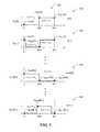
- FIG. 1is a pictorial showing a circular vertical Hall (CVH) sensing element having a plurality of vertical Hall elements arranged in a circle over a common implant region and a two pole magnet disposed close to the CVH sensing element;
- CVHcircular vertical Hall
- FIG. 1Ais a pictorial showing a plurality of sensing elements (or alternatively, sensors), for example, Hall elements, planar or vertical;
- FIG. 2is a graph showing an output signal as may be generated by the CVH sensing element of FIG. 1 or by the sensing elements of FIG. 1A ;
- FIG. 3is a block diagram showing a magnetic field sensor including the CVH sensing element of FIG. 1 and having a combining circuit and a b n control signal generator;
- FIG. 4is block diagram showing an exemplary combining circuit that can be used as the combining circuit of FIG. 3 , which includes switching circuits and a summing circuit;
- FIG. 5is a series of graphs showing behavior of exemplary b n control signals generated by the b n control signal generator of FIG. 3 ;
- FIG. 6is a block diagram of an exemplary b n control signal generation circuit that can be used as the b n control signal generator of FIG. 3 ;
- FIG. 6Ais a series of graphs showing behavior of b n control signals generated by the b n control signal generator of FIG. 6 ;
- FIG. 7is a block diagram showing at least an exemplary combining circuit that can be used as the combining circuit of FIG. 3 ;
- FIG. 8is a graph showing an exemplary output signal from the switching circuits of FIG. 4 for particular b n control signals;
- FIG. 8Ais a graph showing another exemplary output signal from the switching circuits of FIG. 4 for different b n control signals;
- FIG. 9is a graph showing an exemplary output signal from the combining circuit of FIG. 3 ;
- FIG. 10is a block diagram showing a side view of a part of a CVH sensing element, which can be used to provide continuous output signals from a plurality of vertical Hall elements, either with or without chopping.
- sensing elementis used to describe a variety of types of electronic elements that can sense a characteristic of the environment.
- sensing elementsinclude, but are not limited to, pressure sensing elements, temperature sensing elements, light sensing elements, acoustic sensing elements, and magnetic field sensing elements.
- the term “sensor assembly”is used to describe a circuit or assembly that includes a sensing element and other components.
- the term “magnetic field sensor assembly”is used to describe a circuit or assembly that includes a magnetic field sensing element and electronics coupled to the magnetic field sensing element.
- the term “sensor”is used to describe either a sensing element or a sensor assembly.
- magnetic field sensing elementis used to describe a variety of electronic elements that can sense a magnetic field.
- the magnetic field sensing elementscan be, but are not limited to, Hall effect elements, magnetoresistance elements, or magnetotransistors.
- Hall effect elementsfor example, a planar Hall element, a vertical Hall element, and a circular Hall element.
- magnetoresistance elementsfor example, a giant magnetoresistance (GMR) element, an anisotropic magnetoresistance element (AMR), a tunneling magnetoresistance (TMR) element, an Indium antimonide (InSb) sensor, and a magnetic tunnel junction (MTJ).
- GMRgiant magnetoresistance
- AMRanisotropic magnetoresistance element
- TMRtunneling magnetoresistance
- InSbIndium antimonide
- MTJmagnetic tunnel junction
- some of the above-described magnetic field sensing elementstend to have an axis of maximum sensitivity parallel to a substrate that supports the magnetic field sensing element, and others of the above-described magnetic field sensing elements tend to have an axis of maximum sensitivity perpendicular to a substrate that supports the magnetic field sensing element.
- planar Hall elementstend to have axes of sensitivity perpendicular to a substrate
- magnetoresistance elements and vertical Hall elementsincluding circular vertical Hall (CVH) sensing elements
- Magnetic field sensorsare used in a variety of applications, including, but not limited to, an angle sensor that senses an angle of a direction of a magnetic field, a current sensor that senses a magnetic field generated by a current carried by a current-carrying conductor, a magnetic switch that senses the proximity of a ferromagnetic object, a rotation detector that senses passing ferromagnetic articles, for example, magnetic domains of a ring magnet, and a magnetic field sensor that senses a magnetic field density of a magnetic field.
- an angle sensorthat senses an angle of a direction of a magnetic field
- a current sensorthat senses a magnetic field generated by a current carried by a current-carrying conductor
- a magnetic switchthat senses the proximity of a ferromagnetic object
- a rotation detectorthat senses passing ferromagnetic articles, for example, magnetic domains of a ring magnet
- a magnetic field sensorthat senses a magnetic field density of a magnetic field.
- a circular vertical Hall (CVH) sensing element 12includes a circular implant region 18 having a plurality of vertical Hall elements disposed thereon, of which a vertical Hall element 12 a is but one example.
- Each vertical Hall elementhas a plurality of Hall element contacts (e.g., four or five contacts), of which a vertical Hall element contact 12 a is but one example.
- a particular vertical Hall element (e.g., 12 a ) within the CVH sensing element 12which, for example, can have five adjacent contacts, can share some, for example, four, of the five contacts with a next vertical Hall element (e.g., 12 b ).
- a next vertical Hall elementcan be shifted by one contact from a prior vertical Hall element.
- the number of vertical Hall elementsis equal to the number of vertical Hall element contacts, e.g., 32.
- a next vertical Hall elementcan be shifted by more than one contact from the prior vertical Hall element, in which case, there are fewer vertical Hall elements than there are vertical Hall element contacts in the CVH sensing element.
- a center of a vertical Hall element 0is positioned along an x-axis 20 and a center of vertical Hall element 8 is positioned along a y-axis 22 .
- a CVHcan have more than or fewer than thirty-two vertical Hall elements and more than or fewer than thirty-two vertical Hall element contacts.
- a circular magnet 14 having a north side 14 a and a south side 14 bcan be disposed over the CVH 12 .
- the circular magnet 14tends to generate a magnetic field 16 having a direction from the north side 14 a to the south side 14 b , here shown to be pointed to a direction of about forty-five degrees relative to x-axis 20 .
- the circular magnet 14is mechanically coupled to a rotating object, for example, an automobile steering shaft or an automobile camshaft, and is subject to rotation relative to the CVH sensing element 12 .
- a rotating objectfor example, an automobile steering shaft or an automobile camshaft
- the CVH sensing element 12in combination with an electronic circuit described below can generate a signal related to the angle of rotation of the magnet 14 .
- a plurality of sensing elements 30 a - 30 hcan be any type of sensing elements, including, but not limited to, pressure sensing elements, temperature sensing elements, light sensing elements, acoustic sensing elements, and magnetic field sensing elements.
- the magnetic field sensing elements 30 a - 30 hcan be, for example, planar Hall elements, vertical Hall elements, or magnetoresistance elements. These elements can also be coupled to an electronic circuit, in particular, to a combining circuit described below.
- the sensing elements 30 a - 30 hare vertical Hall elements, there can also be a magnet the same as or similar to the magnet 14 of FIG. 1 , disposed proximate to the sensing elements 30 a - 30 h.
- the sensing elements 30 a - 30 hare shown to be arranged in a circle, in some embodiments, the sensing elements can be arranged in another configuration, for example, in a line. Where the sensing elements 30 a - 30 h are magnetic field sensing elements, such a linear arrangement can be used, for example, to detect a linear position of a ferromagnetic object. Where the sensing elements 30 a - 30 h are acoustic sensors, such a linear arrangement can be used, for example, to characterize a position of a sound wave along a line.
- a graph 50has a horizontal axis with a scale in units of CVH vertical Hall element position, n, around a CVH sensing element, for example, the CVH sensing element 12 of FIG. 1 .
- the graph 50also has a vertical axis with a scale in amplitude in units of millivolts.
- the vertical axisis representative of output signal levels from the plurality of vertical Hall elements of the CVH sensing element.
- the graph 50includes a signal 52 representative of output signal levels from the plurality of vertical Hall elements of the CVH taken with the magnetic field of FIG. 1 pointing in a direction of forty-five degrees.
- vertical Hall element 0is centered along the x-axis 20 and vertical Hall element 8 is centered along the y-axis 22 .
- the exemplary CVH sensing element 12there are thirty-two vertical Hall element contacts and a corresponding thirty-two vertical Hall elements, each vertical Hall element having a plurality of vertical Hall element contacts, for example, five contacts.
- a maximum positive signalis achieved from a vertical Hall element centered at position 4, which is aligned with the magnetic field 16 of FIG. 1 , such that a line drawn between the vertical Hall element contacts (e.g., five contacts) of the vertical Hall element at position 4 is perpendicular to the magnetic field.
- a maximum negative signalis achieved from a vertical Hall element centered at position 20, which is also aligned with the magnetic field 16 of FIG. 1 , such that a line drawn between the vertical Hall element contacts (e.g., five contacts) of the vertical Hall element at position 20 is also perpendicular to the magnetic field.
- a sine wave 54is provided to more clearly show the ideal behavior of the signal 52 .
- the signal 52has variations due to vertical Hall element offsets, which tend to somewhat randomly cause element output signals to be too high or too low relative to the sine wave 54 , in accordance with offset errors for each element. The offset signal errors are undesirable.
- groups of contacts of each vertical Hall elementcan be used in a multiplexed or chopped arrangement to generate chopped output signals from each vertical Hall element. Thereafter, or in parallel (i.e., at the same time), a new group of adjacent vertical Hall element contacts can be selected (i.e., a new vertical Hall element), which can be offset by one element from the prior group. The new group can be used in the multiplexed or chopped arrangement to generate another chopped output signal from the next group, and so on.
- Each step of the signal 52can be representative of a chopped output signal from one respective group of vertical Hall element contacts, i.e., from one respective vertical Hall element. However, in other embodiments, no chopping is performed and each step of the signal 52 is representative of an unchopped output signal from one respective group of vertical Hall element contacts, i.e., from one respective vertical Hall element.
- the graph 52is representative of a CVH output signal with or without the above-described grouping and chopping of vertical Hall elements.
- a phase of the signal 52(e.g., a phase of the signal 54 ) can be found and can be used to identify the pointing direction of the magnetic field 16 of FIG. 1 relative to the CVH 12 .
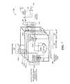
- a circuit 70includes a CVH sensing element 72 having a plurality of vertical Hall elements, each vertical Hall element comprising a group of vertical Hall element contacts (e.g., five vertical Hall element contacts), of which a vertical Hall element contact 73 is but one example.
- the CVH output signals 72 aare comprised of sequential output signals taken one-at-a-time around the CVH sensing element 72 , wherein each output signal is generated on a separate signal path. In other embodiments, all of the CVH output signals 72 a are generated and provided continuously, wherein each one of the CVH output signals 72 a is still generated on a separate signal path. In the latter embodiments, the switching circuit 74 is not required. A continuous arrangement is described more fully below in conjunction with FIG. 10 .
- the number of vertical Hall elements (each comprising a group of vertical Hall element contacts) in the CVH sensing element 72is equal to the total number of sensing element positions, N.
- the CVH output signals 72 acan be comprised of sequential or parallel output signals, wherein each one of the CVH output signals 72 a is associated with a respective one of the vertical Hall elements in the CVH sensing element 72 , i.e., the circuit 10 steps around the vertical Hall elements of the CVH sensing element 72 by increments of one, and N equals the number of vertical Hall elements in the CVH sensing element 72 .
- the incrementscan be by greater than one vertical Hall element, in which case N is less than the number of vertical Hall elements in the CVH sensing element 72 .
- a subscriptis used herein is to represent a vertical Hall element position, whether or not the number of vertical Hall elements is the same as the number of element positions.
- another switching circuit 76can provide the above-described “chopping” of groups of the vertical Hall elements within the CVH sensing element 72 .
- Choppingwill be understood to be an arrangement in which a group of vertical Hall element contacts, for example, five vertical Hall element contacts are driven with current sources 86 in a plurality of connection configurations, and signals are received from the group of vertical Hall element contacts in corresponding configurations.
- nthere can be a plurality of output signals during the chopping, and then the group increments to a new group, for example, by an increment of one vertical Hall element contact.
- the circuit 70includes an oscillator 78 that provides clock signals 78 a , 78 b , 78 c , which can have the same or different frequencies.
- a divider 80is coupled to receive the clock signal 78 a and configured to generate a clock signal 80 a .
- a switch control circuit 82is coupled to receive the clock signal 80 a and configured to generate switch control signals 82 a , which are received by the switching circuits 74 , 76 to control the sequencing around the CVH sensing element 72 , and, optionally, to control chopping of groups of vertical Hall elements within the CVH sensing element 72 in ways described above.
- the current sources 86are used to bias the vertical Hall elements of the CVH sensing element 72 when operating with or without chopping.
- a preprocessing circuit 88is coupled to receive the CVH output signals 72 a .
- a combining circuit 90is coupled to receive the CVH output signals 72 a and configured to generate a preprocessed signal 90 a.
- the circuit 70can include divider 108 coupled to receive the clock signal 78 c and configured to generate a clock signal 108 a .
- a divider 110can be coupled to receive the clock signal 108 a and configured to generate a clock signal 110 a.
- the preprocessing circuitcan include a b n (k) control signal generator 92 coupled to receive the clock signal 108 a at a clock input and coupled to receive the clock signal 110 a at a reset input. Operation of the b n (k) control signal generator 92 is further described below in conjunction with FIGS. 5 , 6 , and 6 A. Let it suffice here to say that the b n (k) control signal generator 92 is configured to generate control signals 92 a , b 0 (k) to b N-1 (k), which are a plurality of control signals to control the combining circuit 90 .
- the combining circuit 90is described more fully below in conjunction with FIG. 4 . Let it suffice here to say that the combining circuit 90 is configured to combine the CVH output signals 72 a in ways that provide and enhanced performance of the circuit 70 that would otherwise not be available.
- the combining circuit 90is configured to generate a combined signal 90 a , E(k).
- an index variable (k)is used to describe an indexing of the b n (k) control signals 92 a .
- the parameter kis used to describe a time indexing of the N control signals, such that at one time index value, the N control signals have a particular state configuration, and at another time index value, the N control signals have another particular state configuration.
- the b n (k) control signals 92 aare described more fully below in conjunction with FIG. 5 .
- the circuit 70can also include an x-y direction component circuit 94 coupled to receive the combined signal 90 a and configured to generate an x-y angle signal 104 a representative of an angle of a magnetic field in a plane of the CVH sensing element.
- the x-y angle signal 104 acan be a digital signal representative of an angle of the magnetic field 16 of FIG. 1 relative to the CVH sensing element 12 .
- the x-y direction component circuit 94can include an amplifier 96 coupled to receive the combined signal 90 a and configured to generate an amplified signal 96 a .
- An optional band pass filter 98can be coupled to receive the amplified signal 96 a and configured to generate a filtered signal 98 a.
- a comparator 100 with hysteresiscan be coupled to receive the filtered signal 98 a and also coupled to receive a predetermined threshold signal 106 and configured to generate a two-state signal 100 a .
- a counter 102can be coupled to receive the two-state signal 100 a at an enable input, to receive the clock signal 78 b at a clock input, and to receive the clock signal 110 a at a reset input.
- the counter 102is configured to generate a phase signal 102 a having a count representative of a phase between the two-state signal 100 a and the clock signal 110 a .
- the phase signalis received by a latch 104 that is latched in accordance with the clock signal 110 a .
- the latch 104is configured to generate a latched signal 104 a.
- the latched signal 104 ais a multi-bit digital signal that has a value representative of an angle of the magnetic field experience by the CVH sensing element 72 .
- all parts of the circuit 70are fabricated on a single common substrate, for example, a silicon substrate.
- a combining circuit 130can be the same as or similar to the combining circuit 90 of FIG. 3 .
- the switching circuits 136 a - 136 Nare also each coupled to receive a respective one of the control signals 92 a , b 0 (k) to b N-1 (k), of FIG. 3 .
- respective sample and hold circuits 138can be coupled before the switching circuits 136 a - 136 N.
- the sample and hold circuits 138can be used for embodiments described above in which the CVH output signals 72 a of FIG. 3 are sequentially generated.
- sampled signals x′ 0 to x′ N-1sampled sequentially and held, are provided to the switching circuits 136 a - 136 N instead of the signals x 0 to x N-1 .
- the switching circuits 136 a - 136 Ngenerate respective switched signals z 0 (k) to z N-1 (k) (e.g., 32 switched signals).
- a summing circuit 134is coupled to receive the switched signals, z 0 (k) to z N-1 (k), and configured to generate a combined signal 134 a , which can be the same as or similar to the combined signal 90 a of FIG. 3 .
- control signals, b 0 (k) to b N-1 (k)are in a high state and others are in a low state.
- the switching circuits 136 a - 136 Nare responsive to respective states of the control signals, b 0 (k) to b N-1 (k), such that, in response to one particular state of a respective control signal, a respective one of the CVH output signals, x 0 to x N-1 , is inverted as it passes through the respective switching circuit, and in response to the other different state of the control signal, the CVH output signal is not inverted.
- Outputs signals, z 0 (k) to z N-1 (k)result, which can be differential signals as shown, or which, in other embodiments, can be signal-ended signals.
- the combined signal 134 ais essentially a sum of signals, i.e., a sum of some of the CVH output signals, x 0 to x N-1 , that are inverted along with some of the CVH output signals, x 0 to x N-1 , that are not inverted.
- control signals, b 0 (k) to b N-1 (k)change state from time to time. Changes of the control signals, b 0 (k) to b N-1 (k), are more fully described below in conjunction with FIGS. 5 , 8 , and 8 A.
- graphs 152 - 158each have a horizontal axis with a scale in units of vertical Hall element position around a CVH sensing element, and a vertical axis having a scale in units representative of a binary state (1 (e.g., high) or 0 (e.g., low)) of the b n control signals, b 0 (k) to b N-1 (k) of FIG. 4 and the b n control signals 92 a of FIG. 3 .
- a binary state (1e.g., high
- 0e.g., low
- the Hall element positions, N positions, represented by the horizontal axescan have steps of one vertical Hall element (i.e., one vertical Hall element contact) or steps of more than one vertical Hall element (i.e., more that one vertical Hall element contact). Furthermore, the positions can be indicative of positions of respective groups of Hall elements when used in a chopped arrangement.
- Each one of the graphsrepresents the control signals, b 0 (k) to b N-1 (k), taken at a different time.
- the graph 152shows that, at a first time (or increment 0 ) of the indexing variable, k, the control signals from b 0 (0) to b N/2-1 (0) are low and the control signals from b N/2 (0) to b N-1 (0) are high.
- the subscript indexis representative of the position, n, of the vertical Hall element (or group of vertical Hall element contacts) around the CVH sensing element, and there are N such positions from 0 to N ⁇ 1.
- the index, kis representative of a time increment associated with a change of the control signals, b 0 (k) to b N-1 (k).
- the graphs 154 - 158are representative of one particular embodiment, for which, at each increment of the time index, k, the control signals b 0 (k) to b N-1 (k) shift by one vertical Hall element position (i.e., by one vertical Hall element contact).
- the control signal b 0 (1)is now high and is the control signal received by the switching circuit 136 a of FIG. 4 .
- the control signal b 0 (N/2 ⁇ 1)is high and is the control signal received by the switching circuit 136 a of FIG. 4 .
- control signals b 0 (k) to b N/2-1 (k) at any increment of the index, kare shown to be high and the other half to be low, in other embodiments, other proportions of high and low control signals can be used. This can include proportions all the way down to one control signal being in one state and all of the other control signals being in another state. However, it will be understood from discussion below that a best signal to noise ratio is obtained when the proportion is one-half.
- the phrase “approximately half”refers to a range of about forty percent to about sixty percent.
- a b n control signal generator 170can be the same as or similar to the b n control signal generator 92 of FIG. 3 and can generate the b n control signals of FIG. 5 , which can be the same as or similar to the b n control signals 92 a of FIG. 3 .
- the b n control signal generator 170can include a first plurality of flip-flops 172 - 176 coupled to receive a clock signal 186 at respective clock inputs. The output from a prior flip-flop is coupled to a data input of a next flip-flop. The plurality of flip-flops 172 - 176 is coupled to receive a reset signal 184 at respective reset inputs.
- a second plurality of flip-flops 178 - 182is also coupled to receive the clock signal 186 at respective clock inputs.
- the output from a prior flip-flopis coupled to a data input of a next flip-flop.
- the plurality of flip-flops 178 - 182is coupled to receive the signal 184 at respective set inputs.
- a last flip-flop 182is coupled to provide its output signal to the data input of the first flip-flop 172 .
- the flip-flops 172 - 176are set low in accordance with the reset signal 184 , and the flip-flops 178 - 182 are set high.
- the signal 186can be the same as or similar to the clock signal 108 a of FIG. 3 and the signal 184 can be the same as or similar to the clock signal 110 a of FIG. 3 . With each subsequent rising edge of clock signal 186 , the position of the N/2 adjacent low signals and N/2 adjacent high signals are shifted one position to the right.
- a chart 200includes graphs 202 - 208 , each graph showing the b n control signals, b 0 (k) to b N-1 (k).
- Each cycle of the clock signal 186 of FIG. 6provides a new set of b n control signals, b 0 (k) to b N-1 (k), i.e., a new index value for the index, k.
- Graphs 202 - 208are very much like graphs shown and described above in conjunction with FIG. 5 , and thus, the graphs 202 - 208 are not discussed further.
- an exemplary circuit 220can include circuit portions 221 a - 221 N, which is a circuit portion replicated N times, where N is the number of vertical Hall element positions, for example thirty-two, in a CVH sensing element.
- the circuit 220can include a combining circuit, which can include switching circuits 234 a - 234 N and also a current summing circuit 242 , which are coupled together.
- the combining circuit of FIG. 7can be the same as or similar to the combining circuits 90 , 130 of FIGS. 3 and 4 , respectively.
- the combining circuit of FIG. 7can generate a combined output signal 244 , E(k), shown here as a differential signal.
- the combined output signal 244can be the same as or similar to the combined output signal 90 a of FIG. 3 and the combined output signal 134 a of FIG. 4 .
- the circuit 220can also include chopping modulators 230 a - 230 N ( 230 b - 230 N not shown), which are coupled to receive the CVH output signals 222 , x 0 to x N-1 , which can be the same as or similar to the CVH output signals x 0 to x N-1 of FIGS. 3 and 4 .
- the chopping modulators 230 a - 230 Nare also coupled to provide bias signals 222 (e.g., current signals) and reference voltage connections 222 to the CVH sensing element. Bias signals and reference connections are described more fully below in conjunction with FIG. 10 .
- choppinguses a group of Hall element contacts, for example, five contacts, here within a CVH sensing element, and switches in various ways between the elements of the group. Thereafter, the chopping moves to a next element position, i.e., indexes around the CVH sensing element by an index step, for example, by one vertical Hall element contact within the CVH sensing element, where chopping is again performed on a next vertical Hall element.
- a next element positioni.e., indexes around the CVH sensing element by an index step, for example, by one vertical Hall element contact within the CVH sensing element
- the choppingis not performed and the chopping modulators 230 a - 230 N are not used.
- Differential pairs 232 a - 232 Nare coupled to receive output signals from the chopping modulators 230 a - 230 N, respectively.
- the differential pairs 232 a - 232 Ncan generate current signals that are received by the switching circuits 234 a - 234 N, respectively. Conversion from voltage signals to current signals allows for simple summation of signals 242 from the plurality of switching circuits 234 a - 234 N to generate the combined output signal 244 .
- the switching circuits 234 a - 234 Nare coupled to receive control signals 224 , b 0 (k) to b N-1 (k), respectively, as described above in conjunction with FIG. 4 . It will be understood from discussion above that the switching circuits 234 a - 234 N are configured to either invert or to not invert current signals provided by the differential pairs 232 a - 232 N, depending upon states of the control signals 224 .
- the chopping modulators 230 a - 230 Nare coupled to receive a Hall element chopping clock 228 , which can be the same clock for each one of the chopping modulators 230 a - 230 N, either sequentially or in parallel.
- the chopping modulators 230 a - 230 Ncan also be coupled to receive two or more Hall element bias signals 240 used in the chopping process.
- the Hall element bias signalscan be the same for each one of the chopping modulators 230 a - 230 N, either sequentially or in parallel.
- the differential pairs 232 a - 232 Ncan be coupled to receive differential pair bias signals 226 .
- the differential pair bias signals 226can be the same for each one of the differential pairs 232 a - 232 N, either sequentially or in parallel.
- a graph 250includes a horizontal axis with a scale in units of CVH element position, n.
- the graph 250also includes a vertical axis with units of magnitude in millivolts.
- the vertical scaleis representative of magnitude of switched element signals z 0 (k) to z N-1 (k) (see, e.g., FIG. 4 ) for a k index value of four. While shown in voltage units in millivolts, the magnitude can either be in units of voltage or in units of current, depending upon the type of circuits used.
- the k index value of fouris representative of a particular shift of the b n control signals (see, e.g., FIG. 5 ).
- a sine wave 254is shown, which is like the sine wave 54 of FIG. 2 .
- a signal 256is representative of the switched element signals (e.g., z 0 (4) to z N-1 (4)) from each one of thirty-two vertical Hall element positions within the CVH sensing element, before the signals are combined, for example, by the summing circuit 134 of FIG. 4 . Comparing the signal 254 to the signal 52 of FIG. 2 , it will be understood that from CVH element position 4 to CVH element position 19, the signal 256 is identical to the signal 52 , while from CVH element positions 20 to 31 and positions 0 to 3, the signal 256 is inverted from the signal 52 . Transitions 256 a and 256 b are apparent.
- a graph 270includes a horizontal axis with a scale in units of CVH element position, n.
- the graph 270also includes a vertical axis with units of magnitude in millivolts.
- the vertical scaleis representative of magnitude of switched element signals z 0 (k) to z N-1 (k) (see, e.g., FIG. 4 ) for a k index value of twenty-eight.
- the k index value of twenty-eightis representative of another particular shift of the b n control signals (see, e.g., FIG. 5 ).
- a sine wave 274is shown, which is like the sine wave 54 of FIG. 2 .
- a signal 272is representative of the switched element signals (e.g., z 0 (28) to z N-1 (28)) from each one of thirty-two vertical Hall element positions within the CVH sensing element, before the signals are combined, for example, by the summing circuit 134 of FIG. 4 . Comparing the signal 272 to the signal 52 of FIG. 2 , it will be understood that from CVH element position 28 to CVH element position 31 and from positions 0 to 11, the signal 272 is identical to the signal 52 , while from element positions 12 to 27, the signal 256 is inverted from the signal 52 .
- the switched element signalse.g., z 0 (28) to z N-1 (28)
- a graph 300includes a horizontal axis in units of the index value k.
- the graph 300also includes a vertical scale in units of voltage in millivolts.
- a signal 302is representative of a summed signal, for example, the summed signal 90 a of FIG. 3 or the summed signal 134 a of FIG. 4 , for all N possible shifts of the b(n) control signals.
- a sine wave 304is shown.
- the signal 302is near zero when the index value, k, is equal to four, and the signal 302 is near to a maximum when the index value, k, is equal to twenty-eight.
- the pointing direction of the magnetic field 16 of FIG. 1can be determined according to a maximum of the signal 52 at the CVH element position of four.
- the magnitude of the signal 302is shown to be larger than the magnitude of the signal 52 of FIG. 2 .
- the larger magnitude of the signal 302is expected due to the summation of signals by the summing circuits, for example, by the summing circuit 134 of FIG. 4 .
- the signal 302can be represented as:
- ⁇ IN+ ⁇ 2 - 2 ⁇ ⁇ N ⁇ ( k - 1 2 )
- the signal 302(the signal 90 a of FIG. 3 ) can be subsequently processed by the x-y direction component circuit 94 to identify a phase of the signal 90 a , which is representative of the angle of the magnetic field.
- the signal 104 a of FIG. 3provides the phase representative of magnetic input angle.
- circuits and methods described hereinare shown by example of vertical Hall elements within a CVH sensing element, as described above, it should be appreciated that the same techniques can be used to process signals from a plurality of any type of sensing element. In some embodiments, the circuits and methods can be used to identify a largest signal from among the plurality of sensing elements. The same benefits of reduced offset signal variations and increased amplitude and processing speed will apply to any type of sensing elements, and not only to magnetic field sensing elements. For example, the same techniques could be applied to a plurality of acoustic sensing elements used to sense an acoustic signal. Depending upon the type of sensing elements, the x-y direction component circuit 94 of FIG. 3 may or may not be applicable. Other types of processing of the summed signal 90 a of FIG. 3 may or may not be provided.
- any type of sensor assembliesi.e., to any type of sensors.
- the same techniquescould be applied to a plurality of magnetic field sensors, each having a magnetic field sensing element and associated processing circuitry, wherein the processing described herein can be applied to output signals from the magnetic field sensors downstream from the magnetic field sensing elements, e.g., to output signals from the magnetic field sensors.
- the CVH sensing element described hereincan be used either in a mode that provides sequential output signals from a plurality of vertical Hall elements or in a mode that can provide simultaneous and continuous output signals from a plurality of vertical Hall elements.
- a sequential arrangementis described in PCT Patent Application No. PCT/EP2008056517, which is incorporated by reference above.
- a continuous arrangementis described more fully below in conjunction with FIG. 10 .
- FIG. 10a portion of a CVH sensing element 320 is shown in panels A-D in four side views having a respective four different exemplary drive and signal arrangements.
- the drive and signal arrangementscan be switched, for example, by the switching circuit 76 of FIG. 3 ., so that the arrangements of panels A-D are achieved sequentially in the above-described chopping of vertical Hall elements. However, if there is no chopping, the arrangement of any one of the panels A-D can be retained continuously.
- the panels A-Dhave the same reference designations to indicate the same elements.
- the CVH sensing element 320includes a plurality of vertical Hall element contacts, of which vertical Hall element contacts 322 a - 322 m are but some of the vertical Hall element contacts in the CVH sensing element 320 .
- the vertical Hall element contacts 322 a - 322 mare arranged over a section of a common circular implant region 324 in a substrate (not shown), which can be the same as or similar to the common circular implant region 18 of FIG. 1 .
- the vertical Hall element contacts 322 a - 322 mcan be the same as or similar to the vertical Hall element contacts (i.e., 12 aa ) of FIG. 1 .
- Vertical hall elements 322 a - 322 mare arranged with groups of five vertical Hall element contacts, each group representing a vertical Hall element.
- a first vertical Hall element 327 aaincludes the vertical Hall element contacts 322 b - 322 f .
- a second vertical Hall element 327 abincludes the vertical Hall element contacts 322 d - 322 h .
- a third vertical 327 acincludes the vertical Hall element contacts 322 f - 322 j.
- current sources 326 , 328drive currents into the vertical Hall element contacts 322 b , 322 f .
- a reference coupling 334is used to couple the vertical Hall element contact 322 d to a reference voltage, for example, a ground voltage.
- Current from the current source 326passes through the vertical Hall element contact 322 b and splits in two, with approximately half of the current flowing toward the reference coupling 334 and approximately half of the current flowing toward another reference coupling (not shown) connected to a vertical Hall element contact positioned to the left of vertical Hall element contact 322 b .
- the current from the current source 328passes through vertical Hall element contact 322 f and splits in two, with approximately half of the current flowing toward the reference coupling 334 and approximately half of the current flowing toward the reference coupling 336 .
- currentsflow from the vertical Hall element contacts 322 b , 322 f to the vertical Hall element contact 322 d as indicated by arrows and dashed lines.
- the upward-flowing current under vertical Hall element contact 322 dcreates a positive voltage when measured from vertical Hall element contact 322 c to vertical Hall element contact 322 e , according to the Hall effect. Therefore an output voltage, V 1a , of the first vertical Hall element 327 aa is oriented so that the positive terminal is on the left, connected to the vertical Hall element contact 322 c , and the negative terminal is on the right, connected to the vertical Hall element contact 322 e.
- the current source 328drives a current into the vertical Hall element contact 322 f
- Reference couplings 334 , 336are used to couple the vertical Hall element contacts 322 d , 322 h to a reference voltage, for example, a ground voltage.
- the current from the current source 328passes through vertical Hall element contact 322 f and splits in two, with approximately half of the current flowing toward reference coupling 336 and approximately half of the current flowing toward reference coupling 334 .
- the current source 328 and the reference coupling 334are continuously shared between the first and second vertical Hall elements 327 aa , 327 ba , respectively.
- currentsflow from the vertical Hall element contact 322 f to the vertical Hall element contacts 322 d , 322 h as indicated by arrows and dashed lines.
- the downward-flowing current under vertical Hall element contact 322 fcreates a positive voltage when measured from the vertical Hall element contact 322 g to the vertical Hall element contact 322 e , according to the Hall effect. Therefore an output voltage, V 2a , of the second vertical Hall element 327 ba is oriented so that the positive terminal is on the right, connected to the vertical Hall element contact 322 g , and the negative terminal is on the left, connected to the vertical Hall element contact 322 e . Note also that the negative terminal connection connected to the vertical Hall element contact 322 e is continuously shared between the first and second vertical Hall elements 327 aa , 327 ba , respectively.
- current sources 328 , 330drive currents into the vertical Hall element contacts 322 f , 322 j .
- a reference coupling 336is used to couple the vertical Hall element contact 322 h to a reference voltage, for example, a ground voltage.
- a reference voltagefor example, a ground voltage.
- currentsflow from the vertical Hall element contacts 322 f , 322 j to the vertical Hall element contact 322 h as indicated by arrows and dashed lines.
- the current from the current source 328passes through the vertical Hall element contact 322 f and splits in two, with approximately half of the current flowing toward the reference coupling 334 and approximately half of the current flowing toward the reference coupling 336 .
- the current from the current source 330passes through vertical Hall element contact 322 j and splits in two, with approximately half of the current flowing toward the reference coupling 336 and approximately half of the current flowing toward the reference coupling 338 .
- currentsflow from the vertical Hall element contacts 322 f , 322 j to the vertical Hall element contact 322 h as indicated by arrows and dashed lines.
- the upward-flowing current under vertical Hall element contact 322 hcreates a positive voltage when measured from the vertical Hall element contact 322 g to the vertical Hall element contact 322 i , according to the Hall effect. Therefore an output voltage, V 3a , of the third vertical Hall element 327 ca is oriented so that the positive terminal is on the left, connected to vertical Hall element contact 322 g , and the negative terminal is on the right, connected to vertical Hall element contact 322 i.
- the arrangement of panel Acan be maintained continuously, in which case, the number of vertical Hall elements is equal to half of the total number of vertical Hall element contacts. For example, if there are sixty-four vertical Hall element contacts in the CVH sensing element 320 , then there are thirty-two vertical Hall elements, each providing a continuous output signal.
- a plurality of output signals from the CVH sensing element 320are continuous signals, in which case, the sample and hold circuits 138 of FIG. 4 are not needed and continuous signals (i.e., x 0 ⁇ x N-1 ) can be presented to the switching circuits 136 a - 136 N of FIG. 4 .
- continuous signalsi.e., x 0 ⁇ x N-1
- panel Ais representative of vertical Hall elements using all of the vertical Hall element contacts in the CVH sensing element, in some embodiments, only two or more vertical Hall elements provide output signals at the same time, wherein the two vertical Hall elements can either share vertical Hall element contacts or not. Each vertical Hall element can generate a differential output signal.
- the current sources 326 , 328 , 330 and the reference couplings 334 , 328 , 330represent particular drive signal generators to drive the vertical Hall elements 327 ab , 327 bb , 327 cb in order to generate output signals.
- Panels B-Dare representative of a chopping arrangement in which all output signals are still available, but for which each output signal (i.e., each vertical Hall element) is chopped to provide four output signal versions.
- Current directions in relation to output voltage polarities in panels B-Dwill be understood from discussion above in conjunction with panel A.
- the current sources 326 , 328 , 330are shifted to the right by one vertical Hall element contact.
- the reference couplings 334 , 336 , 338are also shifted to the right by one and an additional reference coupling 340 is shown coupled to the vertical Hall element contact 322 a.
- the first, second, and third vertical Hall elements 327 ab , 327 bb , 327 cbare shifted to the right from their previous positions by one vertical Hall element contact.
- An output voltage signals V 1b ) from the first vertical Hall element 327 abresults between the vertical Hall element contacts 322 d , 322 f .
- An output voltage signals V 2b from the second vertical Hall element 327 bbresults between the vertical Hall element contacts 322 f , 322 h .
- An output voltage signals V 3b from the third vertical Hall element 327 cbresults between the vertical Hall element contacts 322 h , 322 j.
- the current sources 326 , 328 , 330are again shifted to the right by one vertical Hall element contact.
- the reference couplings 334 , 336 , 338 , 340are also shifted to the right by one.
- the first, second, and third vertical Hall elements 327 ac , 327 bc , 327 ccare shifted to the left from their previous positions by one vertical Hall element contact.
- An output voltage signals V 1c from the first vertical Hall element 327 acresults between the vertical Hall element contacts 322 c , 322 e .
- An output voltage signals V 2c from the second vertical Hall element 327 bcresults between the vertical Hall element contacts 322 e , 322 g .
- An output voltage signals V 3c from the third vertical Hall element 327 ccresults between the vertical Hall element contacts 322 g , 322 i.
- the current sources 326 , 328 , 330are again shifted to the right by one vertical Hall element contact.
- the reference couplings 334 , 336 , 338 , 340are also shifted to the right by one.
- An additional current source 332is shown coupled to the vertical Hall element contact 322 a.
- the first, second, and third vertical Hall elements 327 ad , 327 bd , 327 cdare shifted to the right from their previous positions by one vertical Hall element contact.
- An output voltage signals V 1d from the first vertical Hall element 327 adresults between the vertical Hall element contacts 322 d , 322 f .
- An output voltage signals V 2d from the second vertical Hall element 327 bdresults between the vertical Hall element contacts 322 f , 322 h .
- An output voltage signals V 3d from the third vertical Hall element 327 cdresults between the vertical Hall element contacts 322 h , 322 j.
- first, second, and third vertical Hall elementsare shown to shift right and left in the panels A-D, for the purposes of chopping, they can still considered to be the same vertical Hall element. It will be recognized that by shifting right and left, in the presence of a static magnetic field, the vertical Hall elements will output slightly different signal magnitudes and phases upon each shift. However, unlike the offset voltages represented by the irregular steps of the signal 52 of FIG. 2 , the magnitude and phase shifts caused by the shifting positions are deterministic and can be removed by subsequent processing if desired.
- any offset voltages associated with the first vertical Hall elementwhen combined using an average of the output voltage signals V 1a , V 1b , V 1c , V 1d , will nearly cancel.
- choppingcan achieve a reduction in the offset voltages otherwise represented in the signal 52 of FIG. 2 .
- the combining circuit 90 of FIG. 3combines a plurality of signals from a plurality of vertical Hall elements.
- the combining circuit 90also tends to reduce the effect of offset voltages, resulting in a signal 302 ( FIG. 9 ) having regular rather than random steps.
- no choppingis used and in other embodiments, chopping is used. Also, in some embodiments, only a subset of the arrangements of panels A-D are used, for example, only the arrangements of panel A and panel B are used.
- the choppingi.e., the switching between the arrangements of panels A-D occurs with a chopping rate in the range of about 100 kHz to about 10 MHz.
- vertical Hall elements of FIG. 10are represented as groups of five vertical Hall element contacts, in some embodiments, there can be more than five vertical Hall element contacts in each vertical Hall element. In still other embodiments, there can be three or four vertical Hall element contacts in each vertical Hall element.
- continuously driven vertical Hall elementsare shown to overlap by three vertical Hall element contacts (i.e., they share three vertical Hall element contacts), in other embodiments, the continuously driven vertical Hall elements can overlap by one vertical Hall element contact. (see, e.g., vertical Hall elements 327 aa , 327 ca ).
- circumferential centers (in a direction around the circle of the CVH sensing element) of two continuously driven vertical Hall elementsare angularly disposed around the CVH sensing elements by less than one hundred eighty degrees.
- the two vertical Hall elementsgenerate output signals that are not representative of opposite magnetic field directions relative to each other.
- circumferential centers of the continuously driven vertical Hall elementsare angularly disposed around the CVH sensing elements by an angle less than or equal to about forty-five degrees.
- a CVH sensing elementused in a way to provide continuous output signals
- the CVH sensing elementcan instead be used in a way to provide sequential output signals.
- the sequencing and choppingis more straightforward.
- a first vertical Hall elementcan first be selected having, for example, five vertical Hall element contacts, and can provide an output signal. If chopping is desired, the configuration of the bias signal, reference coupling, and output signals of the first selected vertical Hall element can be reconfigured, for example, to provide multiple output signals that can be averaged.
- a next vertical Hall elementcan be selected, which can be offset from the first selected vertical Hall element, for example, by one vertical Hall element contact from the first selected vertical Hall element, and the chopping can be repeated. If no chopping is used, a particular single configuration of bias, reference, and output signals from each selected vertical Hall element can be used.
- CVH sensing elementis used in examples of an angle sensor above, it should be understood that the same benefits can be achieved with another type of angle sensor, for example, a plurality of separate vertical Hall elements or a plurality of separate magnetoresistance elements.
Landscapes
- Physics & Mathematics (AREA)
- General Physics & Mathematics (AREA)
- Condensed Matter Physics & Semiconductors (AREA)
- Hall/Mr Elements (AREA)
- Transmission And Conversion Of Sensor Element Output (AREA)
Abstract
Description
- where:
- θIN=magnetic field angle in plane of CVH sensing element;
- k=bncontrol signal index;
- N=total number of vertical Hall element positions used in the CVH sensing element; and
- G=a constant related to maximum CVH sensor signal output, e.g., an amplitude of the sine wave signal54 (
FIG. 2 ) or an approximate amplitude of the signal52 (FIG. 2 ), for example:
G=BSgmRout - where:
- B=magnetic field magnitude (Gauss);
- S=vertical Hall element sensitivity (volts/Gauss);
- gm=transconductance of
differential pair 232aofFIG. 5 ; - Rout=transresistance of an output amplifier (volts/amps) (e.g.,236 of
FIG. 7 )
Thus, the magnitude of the result at any angle is:
2GN/π,
which is directly proportional the number of sensing elements in the summation. Using the signal ofFIG. 2 , which has a zero-to-peak amplitude of 5 mV, 2 GN/pi becomes 2*(5 mV)*32/pi=102 mV, which is consistent with the amplitude of the signal302 (or304) ofFIG. 9 .
Claims (12)
Priority Applications (3)
| Application Number | Priority Date | Filing Date | Title |
|---|---|---|---|
| US13/035,243US9062990B2 (en) | 2011-02-25 | 2011-02-25 | Circular vertical hall magnetic field sensing element and method with a plurality of continuous output signals |
| PCT/US2012/024424WO2012115787A1 (en) | 2011-02-25 | 2012-02-09 | Circular vertical hall magnetic field sensing element and method with a plurality of continuous output signals |
| US14/717,448US9182250B2 (en) | 2011-02-25 | 2015-05-20 | Circular vertical hall magnetic field sensing element and method with a plurality of continuous output signals |
Applications Claiming Priority (1)
| Application Number | Priority Date | Filing Date | Title |
|---|---|---|---|
| US13/035,243US9062990B2 (en) | 2011-02-25 | 2011-02-25 | Circular vertical hall magnetic field sensing element and method with a plurality of continuous output signals |
Related Child Applications (1)
| Application Number | Title | Priority Date | Filing Date |
|---|---|---|---|
| US14/717,448DivisionUS9182250B2 (en) | 2011-02-25 | 2015-05-20 | Circular vertical hall magnetic field sensing element and method with a plurality of continuous output signals |
Publications (2)
| Publication Number | Publication Date |
|---|---|
| US20120217955A1 US20120217955A1 (en) | 2012-08-30 |
| US9062990B2true US9062990B2 (en) | 2015-06-23 |
Family
ID=45607420
Family Applications (2)
| Application Number | Title | Priority Date | Filing Date |
|---|---|---|---|
| US13/035,243Active2033-07-19US9062990B2 (en) | 2011-02-25 | 2011-02-25 | Circular vertical hall magnetic field sensing element and method with a plurality of continuous output signals |
| US14/717,448ActiveUS9182250B2 (en) | 2011-02-25 | 2015-05-20 | Circular vertical hall magnetic field sensing element and method with a plurality of continuous output signals |
Family Applications After (1)
| Application Number | Title | Priority Date | Filing Date |
|---|---|---|---|
| US14/717,448ActiveUS9182250B2 (en) | 2011-02-25 | 2015-05-20 | Circular vertical hall magnetic field sensing element and method with a plurality of continuous output signals |
Country Status (2)
| Country | Link |
|---|---|
| US (2) | US9062990B2 (en) |
| WO (1) | WO2012115787A1 (en) |
Cited By (8)
| Publication number | Priority date | Publication date | Assignee | Title |
|---|---|---|---|---|
| US20150198677A1 (en)* | 2014-01-14 | 2015-07-16 | Allegro Microsystems, Llc | Circuit and Method for Reducing an Offset Component of a Plurality of Vertical Hall Elements Arranged in a Circle |
| US9999107B1 (en)* | 2016-12-14 | 2018-06-12 | Allegro Microsystems, Llc | Light emitting diode driver for dimming and on/off control |
| US10430296B2 (en) | 2017-09-29 | 2019-10-01 | Allegro Microsystems, Llc | Circuit and method for storing information in non-volatile memory during a loss of power event |
| US10739164B2 (en) | 2017-01-27 | 2020-08-11 | Allegro Microsystems, Llc | Circuit for detecting motion of an object |
| US10839920B2 (en) | 2017-09-29 | 2020-11-17 | Allegro Microsystems, Llc | Circuit having a low power charge pump for storing information in non-volatile memory during a loss of power event |
| US11473935B1 (en) | 2021-04-16 | 2022-10-18 | Allegro Microsystems, Llc | System and related techniques that provide an angle sensor for sensing an angle of rotation of a ferromagnetic screw |
| US11802922B2 (en) | 2021-01-13 | 2023-10-31 | Allegro Microsystems, Llc | Circuit for reducing an offset component of a plurality of vertical hall elements arranged in one or more circles |
| US12270643B2 (en) | 2023-03-03 | 2025-04-08 | Allegro Microsystems, Llc | Angle sensing having offset and amplitude correction of orthogonal signals using zero crossing detection |
Families Citing this family (16)
| Publication number | Priority date | Publication date | Assignee | Title |
|---|---|---|---|---|
| US8736260B2 (en) | 2012-01-06 | 2014-05-27 | Allegro Microsystems, Llc | Magnetic field sensor and associated method that can establish a measured threshold value and that can store the measured threshold value in a memory device |
| US10845434B2 (en) | 2012-01-06 | 2020-11-24 | Allegro Microsystems, Llc | Magnetic field sensor having a temperature compensated threshold on power up |
| US9395391B2 (en)* | 2013-03-15 | 2016-07-19 | Allegro Microsystems, Llc | Magnetic field sensor and associated method that can store a measured threshold value in a memory device during a time when the magnetic field sensor is powered off |
| US9046383B2 (en)* | 2012-01-09 | 2015-06-02 | Allegro Microsystems, Llc | Systems and methods that use magnetic field sensors to identify positions of a gear shift lever |
| US9417295B2 (en)* | 2012-12-21 | 2016-08-16 | Allegro Microsystems, Llc | Circuits and methods for processing signals generated by a circular vertical hall (CVH) sensing element in the presence of a multi-pole magnet |
| US9606190B2 (en) | 2012-12-21 | 2017-03-28 | Allegro Microsystems, Llc | Magnetic field sensor arrangements and associated methods |
| US8749005B1 (en)* | 2012-12-21 | 2014-06-10 | Allegro Microsystems, Llc | Magnetic field sensor and method of fabricating a magnetic field sensor having a plurality of vertical hall elements arranged in at least a portion of a polygonal shape |
| CN103925933B (en)* | 2013-01-11 | 2016-12-28 | 江苏多维科技有限公司 | A kind of multi-turn absolute magnetic encoder |
| US9389060B2 (en)* | 2013-02-13 | 2016-07-12 | Allegro Microsystems, Llc | Magnetic field sensor and related techniques that provide an angle error correction module |
| DE102014004625A1 (en)* | 2014-03-31 | 2015-10-01 | Micronas Gmbh | sensor device |
| US9448288B2 (en)* | 2014-05-20 | 2016-09-20 | Allegro Microsystems, Llc | Magnetic field sensor with improved accuracy resulting from a digital potentiometer |
| US9638766B2 (en) | 2014-11-24 | 2017-05-02 | Allegro Microsystems, Llc | Magnetic field sensor with improved accuracy resulting from a variable potentiometer and a gain circuit |
| US10385964B2 (en) | 2016-06-08 | 2019-08-20 | Allegro Microsystems, Llc | Enhanced neutral gear sensor |
| DE102017122459A1 (en) | 2017-09-27 | 2019-03-28 | Trw Automotive Gmbh | Method for measuring the webbing extension and webbing retractor |
| US11162815B2 (en)* | 2018-09-14 | 2021-11-02 | Allegro Microsystems, Llc | Angular magnetic field sensor and rotating target with stray field immunity |
| JP7641796B2 (en)* | 2021-03-30 | 2025-03-07 | エイブリック株式会社 | Sensor Device |
Citations (60)
| Publication number | Priority date | Publication date | Assignee | Title |
|---|---|---|---|---|
| JPS5855688A (en) | 1981-09-28 | 1983-04-02 | Kawasaki Heavy Ind Ltd | Heat accumulating system utilizing hydrogenated metal |
| US4668914A (en) | 1983-12-23 | 1987-05-26 | International Standard Electric Corporation | Circular, amorphous metal, Hall effect magnetic field sensor with circumferentially spaced electrodes |
| US4761569A (en) | 1987-02-24 | 1988-08-02 | Sprague Electric Company | Dual trigger Hall effect I.C. switch |
| US4829352A (en) | 1986-04-29 | 1989-05-09 | Lgz Landis & Gyr Zug Ag | Integrable Hall element |
| US5541506A (en) | 1993-10-28 | 1996-07-30 | Nippondenso Co., Ltd. | Rotational position detector having initial setting function |
| US5572058A (en) | 1995-07-17 | 1996-11-05 | Honeywell Inc. | Hall effect device formed in an epitaxial layer of silicon for sensing magnetic fields parallel to the epitaxial layer |
| US5612618A (en) | 1994-10-06 | 1997-03-18 | Nippondenso Co., Ltd. | Rotational position detecting device having peak and bottom hold circuits |
| US5619137A (en) | 1996-02-12 | 1997-04-08 | Allegro Microsystems, Inc. | Chopped low power magnetic-field detector with hysteresis memory |
| US5621319A (en) | 1995-12-08 | 1997-04-15 | Allegro Microsystems, Inc. | Chopped hall sensor with synchronously chopped sample-and-hold circuit |
| US5657189A (en) | 1994-09-19 | 1997-08-12 | Fujitsu Limited | Hall-effect magnetic sensor and a thin-film magnetic head using such a hall-effect magnetic sensor |
| US5694038A (en) | 1996-01-17 | 1997-12-02 | Allegro Microsystems, Inc. | Detector of passing magnetic articles with automatic gain control |
| WO1998010302A2 (en) | 1996-09-09 | 1998-03-12 | Physical Electronics Laboratory | Method for reducing the offset voltage of a hall device |
| US5831513A (en) | 1997-02-04 | 1998-11-03 | United Microelectronics Corp. | Magnetic field sensing device |
| US5844411A (en) | 1995-05-31 | 1998-12-01 | Borg-Warner Automotive, Inc. | Diagnostic detection for hall effect digital gear tooth sensors and related method |
| WO1998054547A1 (en) | 1997-05-29 | 1998-12-03 | Laboratorium Für Physikalische Elektronik | Magnetic rotation sensor |
| US5942895A (en) | 1995-10-30 | 1999-08-24 | Sentron Ag | Magnetic field sensor and current and/or energy sensor |
| WO2000002266A1 (en) | 1998-07-02 | 2000-01-13 | Austria Mikro Systeme International (Ams) | Integrated hall device |
| US6064199A (en) | 1998-02-23 | 2000-05-16 | Analog Devices, Inc. | Magnetic field change detection circuitry having threshold establishing circuitry |
| US6064202A (en) | 1997-09-09 | 2000-05-16 | Physical Electronics Laboratory | Spinning current method of reducing the offset voltage of a hall device |
| US6091239A (en) | 1996-01-17 | 2000-07-18 | Allegro Microsystems, Inc. | Detection of passing magnetic articles with a peak referenced threshold detector |
| US6100680A (en) | 1996-01-17 | 2000-08-08 | Allegro Microsystems, Inc. | Detecting the passing of magnetic articles using a transducer-signal detector having a switchable dual-mode threshold |
| US6166535A (en) | 1997-09-05 | 2000-12-26 | Hella Kg Hueck & Co. | Inductive angle sensor that adapts an oscillator frequency and phase relationship to that of an interference frequency |
| US6232768B1 (en) | 1996-01-17 | 2001-05-15 | Allegro Microsystems Inc. | Centering a signal within the dynamic range of a peak detecting proximity detector |
| US6236199B1 (en) | 1997-09-05 | 2001-05-22 | Hella Kg Hueck & Co. | Inductive angle sensor |
| US6265864B1 (en) | 1999-02-24 | 2001-07-24 | Melexis, N.V. | High speed densor circuit for stabilized hall effect sensor |
| US6356741B1 (en) | 1998-09-18 | 2002-03-12 | Allegro Microsystems, Inc. | Magnetic pole insensitive switch circuit |
| US20020114269A1 (en) | 2000-10-03 | 2002-08-22 | Onggosanusi Eko Nugroho | Channel aware optimal space-time signaling for wireless communication over wideband multipath channels |
| EP0631416B1 (en) | 1993-06-28 | 2002-09-18 | Nec Corporation | Foldable portable telephone set |
| JP2003042709A (en) | 2001-07-30 | 2003-02-13 | Aisin Seiki Co Ltd | Angle sensor |
| US6525531B2 (en) | 1996-01-17 | 2003-02-25 | Allegro, Microsystems, Inc. | Detection of passing magnetic articles while adapting the detection threshold |
| US6542068B1 (en) | 1998-04-27 | 2003-04-01 | Myonic Ag | Vertical hall effect sensor and a brushless electric motor having a vertical hall effect sensor |
| US6545462B2 (en) | 2000-08-21 | 2003-04-08 | Sentron Ag | Sensor for the detection of the direction of a magnetic field having magnetic flux concentrators and hall elements |
| WO2003036733A2 (en) | 2001-10-16 | 2003-05-01 | Fraunhofer Gesellschaft Zur Förderung Der Angewandten Forschung E. V. | Vertical hall sensor |
| WO2003036732A2 (en) | 2001-10-16 | 2003-05-01 | Fraunhofer Gesellschaft Zur Förderung Der Angewandten Forschung E. V. | Compact vertical hall sensor |
| EP0875733B1 (en) | 1997-04-28 | 2004-03-03 | Allegro Microsystems Inc. | Detection of passing magnetic articles using a peak-on-peak percentage threshold detector |
| WO2004025742A1 (en) | 2002-09-10 | 2004-03-25 | Sentron Ag | Magnetic field sensor comprising a hall element |
| US6768301B1 (en) | 1999-09-09 | 2004-07-27 | Fraunhofer-Gesellschaft Zur Foerderung Der Angewandten Forschung E.V. | Hall sensor array for measuring a magnetic field with offset compensation |
| JP2005241269A (en) | 2004-02-24 | 2005-09-08 | Aisin Seiki Co Ltd | Angle sensor |
| US6969988B2 (en) | 2002-03-22 | 2005-11-29 | Asahi Kasei Emd Corporation | Angle determining apparatus and angle determining system |
| US7038448B2 (en) | 2001-05-25 | 2006-05-02 | Sentron Ag | Magnetic field sensor |
| WO2006056289A1 (en) | 2004-11-26 | 2006-06-01 | A. Raymond Et Cie | System for tightly covering a supporting element in the area of a recess |
| WO2006074989A2 (en) | 2005-01-11 | 2006-07-20 | Ecole Polytechnique Federale De Lausanne | Hall sensor and method of operating a hall sensor |
| US7119538B2 (en) | 2003-03-26 | 2006-10-10 | Micronas Gmbh | Offset-reduced hall sensor |
| US7159556B2 (en) | 2004-09-09 | 2007-01-09 | Toyota Jidosha Kabushiki Kaisha | Control apparatus and method for internal combustion engine |
| US20070029998A1 (en) | 2003-08-22 | 2007-02-08 | Sentron Ag | Sensor for detecting the direction of a magnetic field in a plane |
| US20070105244A1 (en) | 2005-11-04 | 2007-05-10 | Nikon Corporation | Analytical apparatus, processing apparatus, measuring and/or inspecting apparatus, exposure apparatus, substrate processing system, analytical method, and program |
| US7259556B2 (en) | 2002-08-01 | 2007-08-21 | Melexis Technologies Sa | Magnetic field sensor and method for operating the magnetic field sensor |
| DE102005014509B4 (en) | 2005-03-30 | 2007-09-13 | Austriamicrosystems Ag | Sensor arrangement and method for determining a rotation angle |
| DE102006037226A1 (en) | 2006-08-09 | 2008-02-14 | Fraunhofer-Gesellschaft zur Förderung der angewandten Forschung e.V. | Calibratable magnetic 3D-point sensor during measuring operation |
| US7362094B2 (en) | 2006-01-17 | 2008-04-22 | Allegro Microsystems, Inc. | Methods and apparatus for magnetic article detection |
| WO2008145662A1 (en) | 2007-05-29 | 2008-12-04 | Ecole Polytechnique Federale De Lausanne | Magnetic field sensor for measuring direction of a magnetic field in a plane |
| EP2000814A2 (en) | 2007-06-04 | 2008-12-10 | Melexis NV | Magnetic field orientation sensor |
| US20090174395A1 (en) | 2008-01-04 | 2009-07-09 | Thomas Monica J | Methods and apparatus for angular position sensing using multiple quadrature signals from frequency independent sinusoids |
| WO2009124969A1 (en) | 2008-04-08 | 2009-10-15 | Ecole Polytechnique Federale De Lausanne (Epfl) | Magnetic field sensor measuring a direction of a magnetic field in a plane and current sensor |
| JP2010014607A (en) | 2008-07-04 | 2010-01-21 | Aisin Seiki Co Ltd | Rotational angle detection apparatus |
| JP2010078366A (en) | 2008-09-24 | 2010-04-08 | Aisin Seiki Co Ltd | Angle detecting apparatus |
| US7714570B2 (en) | 2006-06-21 | 2010-05-11 | Allegro Microsystems, Inc. | Methods and apparatus for an analog rotational sensor having magnetic sensor elements |
| US20100156397A1 (en) | 2008-12-23 | 2010-06-24 | Hitoshi Yabusaki | Methods and apparatus for an angle sensor for a through shaft |
| US7746065B2 (en) | 2004-09-16 | 2010-06-29 | Liaisons Electroniques-Mecaniques Lem S.A. | Continuously calibrated magnetic field sensor |
| US7797604B2 (en) | 2005-12-08 | 2010-09-14 | Electronics And Telecommunications Research Institute | Codeword automatic repeat request/decoding method and transmission/reception apparatus using feedback information |
Family Cites Families (1)
| Publication number | Priority date | Publication date | Assignee | Title |
|---|---|---|---|---|
| DE102010035539B4 (en) | 2010-08-26 | 2012-04-05 | Siemens Aktiengesellschaft | Method for compensating eddy current fields in magnetic resonance imaging and magnetic resonance apparatus |
- 2011
- 2011-02-25USUS13/035,243patent/US9062990B2/enactiveActive
- 2012
- 2012-02-09WOPCT/US2012/024424patent/WO2012115787A1/enactiveApplication Filing
- 2015
- 2015-05-20USUS14/717,448patent/US9182250B2/enactiveActive
Patent Citations (79)
| Publication number | Priority date | Publication date | Assignee | Title |
|---|---|---|---|---|
| JPS5855688A (en) | 1981-09-28 | 1983-04-02 | Kawasaki Heavy Ind Ltd | Heat accumulating system utilizing hydrogenated metal |
| US4668914A (en) | 1983-12-23 | 1987-05-26 | International Standard Electric Corporation | Circular, amorphous metal, Hall effect magnetic field sensor with circumferentially spaced electrodes |
| US4829352A (en) | 1986-04-29 | 1989-05-09 | Lgz Landis & Gyr Zug Ag | Integrable Hall element |
| US4761569A (en) | 1987-02-24 | 1988-08-02 | Sprague Electric Company | Dual trigger Hall effect I.C. switch |
| EP0631416B1 (en) | 1993-06-28 | 2002-09-18 | Nec Corporation | Foldable portable telephone set |
| US5541506A (en) | 1993-10-28 | 1996-07-30 | Nippondenso Co., Ltd. | Rotational position detector having initial setting function |
| US5657189A (en) | 1994-09-19 | 1997-08-12 | Fujitsu Limited | Hall-effect magnetic sensor and a thin-film magnetic head using such a hall-effect magnetic sensor |
| US5612618A (en) | 1994-10-06 | 1997-03-18 | Nippondenso Co., Ltd. | Rotational position detecting device having peak and bottom hold circuits |
| US5844411A (en) | 1995-05-31 | 1998-12-01 | Borg-Warner Automotive, Inc. | Diagnostic detection for hall effect digital gear tooth sensors and related method |
| US5572058A (en) | 1995-07-17 | 1996-11-05 | Honeywell Inc. | Hall effect device formed in an epitaxial layer of silicon for sensing magnetic fields parallel to the epitaxial layer |
| US5942895A (en) | 1995-10-30 | 1999-08-24 | Sentron Ag | Magnetic field sensor and current and/or energy sensor |
| US5621319A (en) | 1995-12-08 | 1997-04-15 | Allegro Microsystems, Inc. | Chopped hall sensor with synchronously chopped sample-and-hold circuit |
| US5694038A (en) | 1996-01-17 | 1997-12-02 | Allegro Microsystems, Inc. | Detector of passing magnetic articles with automatic gain control |
| US6525531B2 (en) | 1996-01-17 | 2003-02-25 | Allegro, Microsystems, Inc. | Detection of passing magnetic articles while adapting the detection threshold |
| US6232768B1 (en) | 1996-01-17 | 2001-05-15 | Allegro Microsystems Inc. | Centering a signal within the dynamic range of a peak detecting proximity detector |
| US6297627B1 (en) | 1996-01-17 | 2001-10-02 | Allegro Microsystems, Inc. | Detection of passing magnetic articles with a peak-to-peak percentage threshold detector having a forcing circuit and automatic gain control |
| US6091239A (en) | 1996-01-17 | 2000-07-18 | Allegro Microsystems, Inc. | Detection of passing magnetic articles with a peak referenced threshold detector |
| US6100680A (en) | 1996-01-17 | 2000-08-08 | Allegro Microsystems, Inc. | Detecting the passing of magnetic articles using a transducer-signal detector having a switchable dual-mode threshold |
| US5619137A (en) | 1996-02-12 | 1997-04-08 | Allegro Microsystems, Inc. | Chopped low power magnetic-field detector with hysteresis memory |
| WO1998010302A2 (en) | 1996-09-09 | 1998-03-12 | Physical Electronics Laboratory | Method for reducing the offset voltage of a hall device |
| US5831513A (en) | 1997-02-04 | 1998-11-03 | United Microelectronics Corp. | Magnetic field sensing device |
| EP0875733B1 (en) | 1997-04-28 | 2004-03-03 | Allegro Microsystems Inc. | Detection of passing magnetic articles using a peak-on-peak percentage threshold detector |
| WO1998054547A1 (en) | 1997-05-29 | 1998-12-03 | Laboratorium Für Physikalische Elektronik | Magnetic rotation sensor |
| US6288533B1 (en) | 1997-05-29 | 2001-09-11 | Physical Electronics Laboratory | Method and apparatus for detecting rotor position by use of magnetic field sensor pairs |
| EP0916074B1 (en) | 1997-05-29 | 2003-07-30 | AMS International AG | Magnetic rotation sensor |
| US6236199B1 (en) | 1997-09-05 | 2001-05-22 | Hella Kg Hueck & Co. | Inductive angle sensor |
| US6166535A (en) | 1997-09-05 | 2000-12-26 | Hella Kg Hueck & Co. | Inductive angle sensor that adapts an oscillator frequency and phase relationship to that of an interference frequency |
| US6064202A (en) | 1997-09-09 | 2000-05-16 | Physical Electronics Laboratory | Spinning current method of reducing the offset voltage of a hall device |
| US6064199A (en) | 1998-02-23 | 2000-05-16 | Analog Devices, Inc. | Magnetic field change detection circuitry having threshold establishing circuitry |
| US6542068B1 (en) | 1998-04-27 | 2003-04-01 | Myonic Ag | Vertical hall effect sensor and a brushless electric motor having a vertical hall effect sensor |
| WO2000002266A1 (en) | 1998-07-02 | 2000-01-13 | Austria Mikro Systeme International (Ams) | Integrated hall device |
| US6622012B2 (en) | 1998-09-18 | 2003-09-16 | Allegro Microsystems, Inc. | Magnetic pole insensitive switch circuit |
| US7085119B2 (en) | 1998-09-18 | 2006-08-01 | Allegro Microsystems, Inc. | Magnetic pole insensitive switch circuit |
| US7307824B2 (en) | 1998-09-18 | 2007-12-11 | Allegro Microsystems, Inc. | Magnetic pole insensitive switch circuit |
| US6356741B1 (en) | 1998-09-18 | 2002-03-12 | Allegro Microsystems, Inc. | Magnetic pole insensitive switch circuit |
| US6265864B1 (en) | 1999-02-24 | 2001-07-24 | Melexis, N.V. | High speed densor circuit for stabilized hall effect sensor |
| US6768301B1 (en) | 1999-09-09 | 2004-07-27 | Fraunhofer-Gesellschaft Zur Foerderung Der Angewandten Forschung E.V. | Hall sensor array for measuring a magnetic field with offset compensation |
| US6545462B2 (en) | 2000-08-21 | 2003-04-08 | Sentron Ag | Sensor for the detection of the direction of a magnetic field having magnetic flux concentrators and hall elements |
| US20020114269A1 (en) | 2000-10-03 | 2002-08-22 | Onggosanusi Eko Nugroho | Channel aware optimal space-time signaling for wireless communication over wideband multipath channels |
| US7038448B2 (en) | 2001-05-25 | 2006-05-02 | Sentron Ag | Magnetic field sensor |
| US7030606B2 (en) | 2001-07-30 | 2006-04-18 | Aisin Seiki Kabushiki Kaisha | Angular sensor with a magneto-electric transducer and a magnetic deflection device |
| JP2003042709A (en) | 2001-07-30 | 2003-02-13 | Aisin Seiki Co Ltd | Angle sensor |
| WO2003036732A2 (en) | 2001-10-16 | 2003-05-01 | Fraunhofer Gesellschaft Zur Förderung Der Angewandten Forschung E. V. | Compact vertical hall sensor |
| WO2003036733A3 (en) | 2001-10-16 | 2003-10-30 | Fraunhofer Ges Forschung | Vertical hall sensor |
| WO2003036733A2 (en) | 2001-10-16 | 2003-05-01 | Fraunhofer Gesellschaft Zur Förderung Der Angewandten Forschung E. V. | Vertical hall sensor |
| US6969988B2 (en) | 2002-03-22 | 2005-11-29 | Asahi Kasei Emd Corporation | Angle determining apparatus and angle determining system |
| US7259556B2 (en) | 2002-08-01 | 2007-08-21 | Melexis Technologies Sa | Magnetic field sensor and method for operating the magnetic field sensor |
| WO2004025742A1 (en) | 2002-09-10 | 2004-03-25 | Sentron Ag | Magnetic field sensor comprising a hall element |
| US20060011999A1 (en) | 2002-09-10 | 2006-01-19 | Sentron Ag | Magnetic field sensor comprising a hall element |
| US7872322B2 (en) | 2002-09-10 | 2011-01-18 | Melexis Tessenderlo Nv | Magnetic field sensor with a hall element |
| US7119538B2 (en) | 2003-03-26 | 2006-10-10 | Micronas Gmbh | Offset-reduced hall sensor |
| US7235968B2 (en) | 2003-08-22 | 2007-06-26 | Melexis Technologies Sa | Sensor for detecting the direction of a magnetic field in a plane |
| US20070029998A1 (en) | 2003-08-22 | 2007-02-08 | Sentron Ag | Sensor for detecting the direction of a magnetic field in a plane |
| JP2005241269A (en) | 2004-02-24 | 2005-09-08 | Aisin Seiki Co Ltd | Angle sensor |
| US7159556B2 (en) | 2004-09-09 | 2007-01-09 | Toyota Jidosha Kabushiki Kaisha | Control apparatus and method for internal combustion engine |
| US7746065B2 (en) | 2004-09-16 | 2010-06-29 | Liaisons Electroniques-Mecaniques Lem S.A. | Continuously calibrated magnetic field sensor |
| WO2006056289A1 (en) | 2004-11-26 | 2006-06-01 | A. Raymond Et Cie | System for tightly covering a supporting element in the area of a recess |
| WO2006074989A2 (en) | 2005-01-11 | 2006-07-20 | Ecole Polytechnique Federale De Lausanne | Hall sensor and method of operating a hall sensor |
| DE102005014509B4 (en) | 2005-03-30 | 2007-09-13 | Austriamicrosystems Ag | Sensor arrangement and method for determining a rotation angle |
| US7759929B2 (en) | 2005-03-30 | 2010-07-20 | Austriamicrosystems Ag | System and method for determining an angle of rotation with cascade sensors |
| US20070105244A1 (en) | 2005-11-04 | 2007-05-10 | Nikon Corporation | Analytical apparatus, processing apparatus, measuring and/or inspecting apparatus, exposure apparatus, substrate processing system, analytical method, and program |
| US7797604B2 (en) | 2005-12-08 | 2010-09-14 | Electronics And Telecommunications Research Institute | Codeword automatic repeat request/decoding method and transmission/reception apparatus using feedback information |
| US7362094B2 (en) | 2006-01-17 | 2008-04-22 | Allegro Microsystems, Inc. | Methods and apparatus for magnetic article detection |
| US7911203B2 (en) | 2006-06-21 | 2011-03-22 | Allegro Microsystems, Inc. | Sensor having an analog processing module to generate a linear position output |
| US7994774B2 (en) | 2006-06-21 | 2011-08-09 | Allegro Microsystems, Inc. | Methods and apparatus for an analog rotational sensor having magnetic sensor elements |
| US20110248708A1 (en) | 2006-06-21 | 2011-10-13 | Allegro Microsystems, Inc. | Methods for an analog rotational sensor having magnetic sensor elements |
| US7714570B2 (en) | 2006-06-21 | 2010-05-11 | Allegro Microsystems, Inc. | Methods and apparatus for an analog rotational sensor having magnetic sensor elements |
| DE102006037226A1 (en) | 2006-08-09 | 2008-02-14 | Fraunhofer-Gesellschaft zur Förderung der angewandten Forschung e.V. | Calibratable magnetic 3D-point sensor during measuring operation |
| US20100164491A1 (en) | 2007-05-29 | 2010-07-01 | Ecole Polytechnique Federale De Lausanne (Epfl) | Magnetic Field Sensor For Measuring A Direction Of A Magnetic Field In A Plane |
| WO2008145662A1 (en) | 2007-05-29 | 2008-12-04 | Ecole Polytechnique Federale De Lausanne | Magnetic field sensor for measuring direction of a magnetic field in a plane |
| EP2000814A3 (en) | 2007-06-04 | 2010-09-22 | Melexis NV | Magnetic field orientation sensor |
| US20090121707A1 (en) | 2007-06-04 | 2009-05-14 | Melexis Nv | Magnetic field orientation sensor |
| US7965076B2 (en) | 2007-06-04 | 2011-06-21 | Melexis Nv, Microelectronic Integrated Systems | Magnetic field orientation sensor |
| EP2000814A2 (en) | 2007-06-04 | 2008-12-10 | Melexis NV | Magnetic field orientation sensor |
| US20090174395A1 (en) | 2008-01-04 | 2009-07-09 | Thomas Monica J | Methods and apparatus for angular position sensing using multiple quadrature signals from frequency independent sinusoids |
| WO2009124969A1 (en) | 2008-04-08 | 2009-10-15 | Ecole Polytechnique Federale De Lausanne (Epfl) | Magnetic field sensor measuring a direction of a magnetic field in a plane and current sensor |
| JP2010014607A (en) | 2008-07-04 | 2010-01-21 | Aisin Seiki Co Ltd | Rotational angle detection apparatus |
| JP2010078366A (en) | 2008-09-24 | 2010-04-08 | Aisin Seiki Co Ltd | Angle detecting apparatus |
| US20100156397A1 (en) | 2008-12-23 | 2010-06-24 | Hitoshi Yabusaki | Methods and apparatus for an angle sensor for a through shaft |
Non-Patent Citations (69)
| Title |
|---|
| Allegro Microsystems, Inc., "High Precision 2-Wire Linear Hall Effect Sensor IC with a Pulse Width Modulated Output", A1354, pp. 1-22. |
| Allegro Microsystems, Inc., "High Precision Linear Hall Effect Sensor IC with a Push/Pull, Pulse Width Modulated Output", A1351 pp. 1-23. |
| Allegro Microsystems, Inc., "High Precision Linear Hall-Effect Sensor with an Open Drain Pulse Width Modulated Output", A1356, pp. 1-20. |
| Allegro Microsystems, Inc., "Low-Noise Programmable Linear Hall Effect Sensor IC's with Adjustable Bandwidth (50 kHz Maximum) and Analog Output", A1360, A1361 and A1362, pp. 1-25. |
| Allegro Microsystems, Inc.; "27701-An Data Sheet: Hall-Effect IC Applications Guide;" Application Information, Rev. 2; http://www.allepromicro.com/en/products/desion/hall-effect-sensor-ic-applications-guide/AN27701.pdf; downloaded Sep. 29, 2010; pp. 1-40. |
| Allegro Microsystems, Inc.; "3235 Data Sheet 27633A, Dual-Output Hall-Effect Switch;" http://www.datasheetcatalog.orp/datasheets/90/205047-DS.pdf; downloaded Sep. 29, 2010; 6 sheets. |
| Allegro Microsystems, Inc.; "A1140/41/42/43 Data Sheet: Sensitive Two-Wire Chopper-Stabilized Unipolar Hall-Effect Switches;" published Sep. 9, 2004; pp. 1-11. |
| Allegro Microsystems, Inc.; "A1174 Data Sheet: Ultrasensitive Hall Effect Latch with Internally or Externally Controlled Sample and Sleep Periods for Track Ball and Scroll Wheel Applications;" published Jul. 25, 2008; pp. 1-13. |
| Allegro Microsystems, Inc.; "A1230 Data Sheet: Ultra-Sensitive Dual-Channel Quadrature Hall-Effect Bipolar Switch;" published Mar. 26, 2010; 16 sheets. |
| Allegro Microsystems, Inc.; "A1351 Data Sheet: High Precision Linear Hall Effect Sensor with a Push/Pull, Pulse Width Modulated Output;" published Mar. 7, 2008; pp. 1-23. |
| Allegro Microsystems, Inc.; "A1360, A1361 and A1362 Data Sheet: Low-Noise Programmable Linear Hall Effect Sensors with Adjustable Bandwidth (50 kHz Maximum) and Analog Output;" published Mar. 18, 2008; pp. 1-25. |
| Allegro Microsystems, Inc.; "A3212 Data Sheet: Micropower, Ultra-Sensitive Hall-Effect Switch;" published Sep. 22, 2004; pp. 1-12. |
| Allegro Microsystems, Inc.; "A3425 Data Sheet: Dual, Chopper-Stabilized, Ultra-Sensitive Bipolar Hall-Effect Switch;" published Jun. 28, 2002; pp. 1-10. |
| Allegro Microsystems, Inc.; "ATS675LSE Data Sheet: Self-Calibrating TPOS Speed Sensor Optimized for Automotive Cam Sensing Applications;" published Jul. 11, 2008; pp. 1-13. |
| Atherton et al.; "Sensor Signal Conditioning-an IC Designer's Perspective;" IEEE Electro International; Apr. 26-28, 1991; pp. 129-134. |
| Austria Microsystems; "AS5040 datasheet; 10-Bit Programmable Magnetic Rotary Encoder;" Revision 1.1; Jan. 2004; pp. 1-20. |
| Banjevic et al; "2D CMOS Integrated Magnetometer Based on the Miniaturized Circular Vertical Hall Device;" International Solid-State Sensors, Actuators and Microsystems Conference; Transducers; Jun. 21-25, 2009; pp. 877-880. |
| Banjevic; "High Bandwidth CMOS Magnetic Sensors Based on the Miniaturized Circular Vertical Hall Device;" Sep. 2011; 153 pages. |
| Banjevic; "High Bandwidth CMOS Magnetic Sensors Based on the Miniturized Circular Vertical Hall Device;" Ecole Polytechnique Federale DeLausanne; These N 5114; Jan. 2011; 153 pages. |
| Baschirotto, A., "Development and Analysis of a PCB Vector 2-D Magnetic Field Sensor System for Electronic Compasses", IEEE Sensors Journal, vol. 6, No. 2, Apr. 2006, pp. 365-371. |
| Blanchard et al.; "Cylindrical Hall Device;" International Electron Devices Meeting; Dec. 8-11, 1996; pp. 541-544. |
| Burger et al.; "New fully integrated 3-D silicon Hall sensor for precise angular-position measurements;" Sensors and Actuators, A 67; May 1998; pp. 72-76. |
| Drljaca, et al.; "Nonlinear Effects in Magnetic Angular Position Sensor With Integrated Flux Concentrator;" Proc. 23rd International Conference on Microelectronics (MIEL 2002); vol. 1; NIS; Yugoslavia; May 12-15, 2002; pp. 223-226. |
| Dwyer; Allegro Microsystems, Inc.; "AN296061 Data Sheet: Ring Magnet Speed Sensing for Electronic Power Steering;" published Jul. 21, 2009; pp. 1-4. |
| Freitas et al.; "Giant magnetoresistive sensors for rotational speed control;" Jorunal of Applied Physics, vol. 85, No. 8; Apr. 15, 1999; pp. 5459-5461. |
| Gerhauser, H., "Intelligente 3D-Magnetfeld Snesorik", Fraunhofer-Institut for Integrierte Schaltungen IIS, www.iis.fraunhofer.de/asic/analoq, 12 pages. |
| Gilbert; "Technical Advances in Hall-Effect Sensing;" Allegro Microsystems, Inc. Product Description; May 10, 2008; 7 sheets. |
| Häberli et al.; "Contactless Angle Measurements by CMOS Magnetic Sensor with on Chip Read-Out Circuit;" The 8th International Conference on Solid-State Sensors and Actuators and Eurosensors IX; Jan. 25-29, 1995; pp. 134-137. |
| Häberli et al.; "Two-Dimensional Magnetic Microsensor with On-Chip Signal Processing for Contactless Angle Measurement;" IEEE Journal of Solid-State Circuits, vol. 31, No. 12; Dec. 1996; pp. 1902-1907. |
| Hiligsmann et al.; "Monolithic 360 Degrees Rotary Position Sensor IC;" 2004 IEEE Proceedings of Sensors, vol. 3; Oct. 24-27, 2004; pp. 1137-1142. |
| Kaufmann et al.; "Novel Coupling Concept for Five-Contact Vertical Hall Devices;" 16th International Solied-State Sensors, Actuators and Microsystems (Transducers) Conference; Jun. 5-9, 2011; 4 sheets. |
| Kejik et al.; "Circular Hall Transducer for Angular Position Sensing;" International Solid-State Sensors, Actuators and Microsystems Conference; Transducers; Jun. 2007; pp. 2593-2596. |
| Kejik, P. et al., "Purley CMOS Angular Position Sensor Based on a New Hall Microchip", 34th Annual Conference of IEEE Industrial Electronics, IECON2008, 2008, pp. 1777-1781. |
| Kejik, P.et al., "Ultra Low-Power Angular Position Sensor for High-Speed Portable Applications", IEEE Sensors 2009 Conference, pp. 173-176. |
| Lou Law; "Angle Position Sensing with 2-Axis Hall ICs;" Sensors Magazine, vol. 20, No. 3; Mar. 2003; 7 sheets. |
| Masson et al.; "Multiturn and high precision through-shaft magnetic sensors;" Sensor + Text Conference; Proceedings II; May 2009; pp. 41-46. |
| Melexis Microelectronic Integrated Systems, "Triaxis 3D-Joystick Position Sensor", Data Sheet, Mar. 2009, 43 pages. |
| Melexis MLX 90324; ""Under-the-Hood" Triaxis Rotary Position feat. SENT Protocol;" 3901090324 Data Sheet; Dec. 2008; 40 pages. |
| Memsic Corporation, "Electronic Tilt Compensation", Mar. 2008, 5 pages. |
| Memsic Corporation, "Magnetic Sensor Calibration", Mar. 2008, 5 pages. |
| Memsic Corporation, "Magnetic Sensor Placement Guidelines", Oct. 2008, 2 pages. |
| Memsic Corporation, "Magnetometer Fundamentals", Jun. 2008, 6 pages. |
| Memsic Corporation, "Magnetometer Soldering Methodology", Jun. 2008 2 pages. |
| Memsic Corporation, "Tri-axis Magnetic Sensor, with I2C Interface", Aug. 14, 2008, 9 pages. |
| Memsic Corporation, "Ultra Small 3-axis Magnetic Sensor, with I2C Interface", Mar. 31, 2010, 8 pages. |
| Memsic Corporation, Letter dated Jun. 12, 2010, 2 pages. |
| Metz et al.; "Contactless Angle Measurement Using Four Hall Devices on Single Chip;"; International Conference on Solid State Sensors and Actuators; Transducers; vol. 1; Jun. 16-19, 1997; pp. 385-388. |
| Micronas GmbH, HAL ® 3625 Programmable Direct Angle Sensor, Product Information, Sep. 2009, 2 pages. |
| Munter; "A Low-offset Spinning-current Hall Plate;" Sensors and Actuators, vol. A21-A23; Jan. 1990; pp. 743-746. |
| Notice of Allowance dated Jun. 11, 2014 from U.S. Appl. No. 13/113,603, filed May 23, 2011. |
| Novotechnik Siedle Group; "How New Angular Positioning Sensor Technology Opens a Broad Range of New Applications;" Vert-X Technology; Dec. 2001; pp. 1-5. |
| Paranjape et al.; "A CMOS-compatible 2-D vertical Hall magnetic-field sensor using active carrier confinement and post-process micromachining;" The 8th International Conference on Solid-State Sensors and Acutators, Physical vol. 53, Issues 1-3; May 1996; pp. 278-283. |
| PCT International Preliminary Report on Patentability and Written Opinion of the ISA dated Apr. 10, 2014; for PCT Pat. App. No. PCT/US2012/052639; 19 pages. |
| PCT International Preliminary Report on Patentability and Written Opinion of the ISA; dated Sep. 6, 2013; for PCT Pat. App. No. PCT/US2012/024424; 11 pages. |
| PCT Search Report and Written Opinion of the ISA; dated Jul. 2, 2012; for PCT Pat. App. No. PCT/US2012/024424; 14 pages. |
| Petoussis et al.; "A Novel Hall Effect Sensor Using Elaborate Offset Cancellation Method;" Sensors & Transducers Journal, vol. 100, Issue 1; Jan. 2009; pp. 85-91. |
| Popovic; "Not-plate-like Hall magnetic sensors and their applications;" Sensors and Actuators A: Physical, vol. 85, Issues 1-3; Aug. 2000; pp. 9-17. |
| Reymond et al.; "Circular Hall Transducer for Angular Position Sensing;" Sensors Conference; Mar. 2007; pp. 2593-2596. |
| Reymond, S. et al., "True 2D CMOS Integrated Hall Sensor", IEEE Sensors 2007 Conference, pp. 860-863. |
| Roumenin et al.; "Vertical Hall Effect Devices in the Basis of Smart Silicon Sensors;" IEEE Workshop on Intelligent Data Acquisition and Advanced Computing Systems: Technology and Applications; Sep. 5-7, 2005; pp. 55-58. |
| Roumenin; "Magnetic sensors continue to advance towards perfection;" Sensors and Actuators A: Physical, vol. 46-47, Issues 1-3; Jan.-Feb. 1995; pp. 273-279. |
| Schneider et al.; "Temperature Calibration of CMOS Magnetic Vector Probe for Contactless Angle Measurement System;" International Electron Devices Meeting; Dec. 8-11, 1996; pp. 533-536. |
| Schurig et al.; "CMOS Integrated Vertical Hall Sensor with Low Offset;" 16th European Conference on Solid-State Transducers; Sep. 15-18, 2002; pp. 868-871. |
| Sensima technology sa; "CVHD: a new concept of Angular Position Sensor;" Slide Presentation for Allegro Microsystems; Mar. 2009; 17 sheets. |
| Sentron; An-101; "Angular position sensing with 2-Axis Hall IC 2SA-10;" Feb. 12, 2004; http://www.diegm.uniud.it/petrella/Azionamenti%20Elettrici%20II/Sensori%20e/%20trasduttori/Data/%20Sheet%20-%202SA-10.pdf; pp. 1-7. |
| U.S. Appl. No. 14/155,047, filed Jan. 14, 2014, Romero. |
| van der Meer; et al; "CMOS quad spinning-current Hall-sensor system for compass application;" IEEE Proceedings of Sensors, vol. 3; Oct. 24-27, 2004; pp. 1434-1437. |
| Vogelgesang et al.; Robert Bosch GmbH; "GMR sensors in automotive application;" CS-SNS/ECS Slides Presentation; Mar. 2, 2005; 16 sheets. |
| Voider; "The CORDIC Trigonometric Computing Technique;" The Institute of Radio Engineers, Inc.; IRE Transactions on Electronic Computers, vol. EC, Issue 3; Sep. 1959; pp. 226-230. |
Cited By (12)
| Publication number | Priority date | Publication date | Assignee | Title |
|---|---|---|---|---|
| US20150198677A1 (en)* | 2014-01-14 | 2015-07-16 | Allegro Microsystems, Llc | Circuit and Method for Reducing an Offset Component of a Plurality of Vertical Hall Elements Arranged in a Circle |
| US9547048B2 (en)* | 2014-01-14 | 2017-01-17 | Allegro Micosystems, LLC | Circuit and method for reducing an offset component of a plurality of vertical hall elements arranged in a circle |
| US9999107B1 (en)* | 2016-12-14 | 2018-06-12 | Allegro Microsystems, Llc | Light emitting diode driver for dimming and on/off control |
| US10219344B2 (en) | 2016-12-14 | 2019-02-26 | Allegro Microsystems, Llc | Light emitting diode driver for dimming and on/off control |
| US10739164B2 (en) | 2017-01-27 | 2020-08-11 | Allegro Microsystems, Llc | Circuit for detecting motion of an object |
| US10430296B2 (en) | 2017-09-29 | 2019-10-01 | Allegro Microsystems, Llc | Circuit and method for storing information in non-volatile memory during a loss of power event |
| US10839920B2 (en) | 2017-09-29 | 2020-11-17 | Allegro Microsystems, Llc | Circuit having a low power charge pump for storing information in non-volatile memory during a loss of power event |
| US10929252B2 (en) | 2017-09-29 | 2021-02-23 | Allegro Microsystems, Llc | Circuit and method for storing information in non-volatile memory during a loss of power event |
| US11467928B2 (en) | 2017-09-29 | 2022-10-11 | Allegro Microsystems, Llc | Circuit and method for storing information in non-volatile memory during a loss of power event |
| US11802922B2 (en) | 2021-01-13 | 2023-10-31 | Allegro Microsystems, Llc | Circuit for reducing an offset component of a plurality of vertical hall elements arranged in one or more circles |
| US11473935B1 (en) | 2021-04-16 | 2022-10-18 | Allegro Microsystems, Llc | System and related techniques that provide an angle sensor for sensing an angle of rotation of a ferromagnetic screw |
| US12270643B2 (en) | 2023-03-03 | 2025-04-08 | Allegro Microsystems, Llc | Angle sensing having offset and amplitude correction of orthogonal signals using zero crossing detection |
Also Published As
| Publication number | Publication date |
|---|---|
| US20120217955A1 (en) | 2012-08-30 |
| US9182250B2 (en) | 2015-11-10 |
| US20150253156A1 (en) | 2015-09-10 |
| WO2012115787A1 (en) | 2012-08-30 |
Similar Documents
| Publication | Publication Date | Title |
|---|---|---|
| US9182250B2 (en) | Circular vertical hall magnetic field sensing element and method with a plurality of continuous output signals | |
| US8786279B2 (en) | Circuit and method for processing signals generated by a plurality of sensors | |
| US8860410B2 (en) | Circuits and methods for processing a signal generated by a plurality of measuring devices | |
| US8749005B1 (en) | Magnetic field sensor and method of fabricating a magnetic field sensor having a plurality of vertical hall elements arranged in at least a portion of a polygonal shape | |
| US9606190B2 (en) | Magnetic field sensor arrangements and associated methods | |
| US8890518B2 (en) | Arrangements for self-testing a circular vertical hall (CVH) sensing element and/or for self-testing a magnetic field sensor that uses a circular vertical hall (CVH) sensing element | |
| JP6513701B2 (en) | Circuit and method for reducing the offset component of circularly arranged vertical Hall elements | |
| US8793085B2 (en) | Circuits and methods for automatically adjusting a magnetic field sensor in accordance with a speed of rotation sensed by the magnetic field sensor | |
| KR102293943B1 (en) | Magnetic field sensors and associated methods with reduced offset and improved accuracy | |
| US10866287B1 (en) | Magnetic field sensor with magnetoresistance elements arranged in a bridge and having a common reference direction and opposite bias directions | |
| US20180356253A1 (en) | Angle sensor bridges including star-connected magnetoresistive elements | |
| US11215681B2 (en) | Magnetic field sensor with stray field immunity and large air gap performance | |
| US10386427B1 (en) | Magnetic field sensor having at least two CVH elements and method of operating same | |
| KR101825313B1 (en) | Magnetic detection apparatus | |
| US11237020B2 (en) | Magnetic field sensor having two rows of magnetic field sensing elements for measuring an angle of rotation of a magnet | |
| US9684042B2 (en) | Magnetic field sensor with improved accuracy and method of obtaining improved accuracy with a magnetic field sensor |
Legal Events
| Date | Code | Title | Description |
|---|---|---|---|
| AS | Assignment | Owner name:ALLEGRO MICROSYSTEMS, INC., MASSACHUSETTS Free format text:ASSIGNMENT OF ASSIGNORS INTEREST;ASSIGNOR:PETRIE, CRAIG S.;REEL/FRAME:025871/0833 Effective date:20110225 | |
| AS | Assignment | Owner name:ALLEGRO MICROSYSTEMS, LLC, MASSACHUSETTS Free format text:CONVERSION AND NAME CHANGE;ASSIGNOR:ALLEGRO MICROSYSTEMS, INC.;REEL/FRAME:030426/0178 Effective date:20130321 | |
| STCF | Information on status: patent grant | Free format text:PATENTED CASE | |
| CC | Certificate of correction | ||
| MAFP | Maintenance fee payment | Free format text:PAYMENT OF MAINTENANCE FEE, 4TH YEAR, LARGE ENTITY (ORIGINAL EVENT CODE: M1551) Year of fee payment:4 | |
| AS | Assignment | Owner name:MIZUHO BANK LTD., AS COLLATERAL AGENT, NEW YORK Free format text:PATENT SECURITY AGREEMENT;ASSIGNOR:ALLEGRO MICROSYSTEMS, LLC;REEL/FRAME:053957/0620 Effective date:20200930 Owner name:CREDIT SUISSE AG, CAYMAN ISLANDS BRANCH, AS COLLATERAL AGENT, NEW YORK Free format text:PATENT SECURITY AGREEMENT;ASSIGNOR:ALLEGRO MICROSYSTEMS, LLC;REEL/FRAME:053957/0874 Effective date:20200930 | |
| MAFP | Maintenance fee payment | Free format text:PAYMENT OF MAINTENANCE FEE, 8TH YEAR, LARGE ENTITY (ORIGINAL EVENT CODE: M1552); ENTITY STATUS OF PATENT OWNER: LARGE ENTITY Year of fee payment:8 | |
| AS | Assignment | Owner name:MORGAN STANLEY SENIOR FUNDING, INC., AS THE COLLATERAL AGENT, MARYLAND Free format text:PATENT SECURITY AGREEMENT;ASSIGNOR:ALLEGRO MICROSYSTEMS, LLC;REEL/FRAME:064068/0459 Effective date:20230621 Owner name:ALLEGRO MICROSYSTEMS, LLC, NEW HAMPSHIRE Free format text:RELEASE OF SECURITY INTEREST IN PATENTS (R/F 053957/0620);ASSIGNOR:MIZUHO BANK, LTD., AS COLLATERAL AGENT;REEL/FRAME:064068/0360 Effective date:20230621 | |
| AS | Assignment | Owner name:ALLEGRO MICROSYSTEMS, LLC, NEW HAMPSHIRE Free format text:RELEASE OF SECURITY INTEREST IN PATENTS AT REEL 053957/FRAME 0874;ASSIGNOR:CREDIT SUISSE AG, CAYMAN ISLANDS BRANCH, AS COLLATERAL AGENT;REEL/FRAME:065420/0572 Effective date:20231031 |