US9059370B2 - Zinc oxide film method and structure for CIGS cell - Google Patents
Zinc oxide film method and structure for CIGS cellDownload PDFInfo
- Publication number
- US9059370B2 US9059370B2US14/025,592US201314025592AUS9059370B2US 9059370 B2US9059370 B2US 9059370B2US 201314025592 AUS201314025592 AUS 201314025592AUS 9059370 B2US9059370 B2US 9059370B2
- Authority
- US
- United States
- Prior art keywords
- containing precursor
- zinc
- substrate
- layer
- species
- Prior art date
- Legal status (The legal status is an assumption and is not a legal conclusion. Google has not performed a legal analysis and makes no representation as to the accuracy of the status listed.)
- Expired - Fee Related
Links
- 238000000034methodMethods0.000titleclaimsabstractdescription69
- XLOMVQKBTHCTTD-UHFFFAOYSA-NZinc monoxideChemical compound[Zn]=OXLOMVQKBTHCTTD-UHFFFAOYSA-N0.000titleclaimsabstractdescription48
- 239000011787zinc oxideSubstances0.000titleclaimsabstractdescription24
- 239000000758substrateSubstances0.000claimsabstractdescription39
- 239000010409thin filmSubstances0.000claimsabstractdescription26
- 239000006096absorbing agentSubstances0.000claimsabstractdescription21
- HQWPLXHWEZZGKY-UHFFFAOYSA-NdiethylzincChemical compoundCC[Zn]CCHQWPLXHWEZZGKY-UHFFFAOYSA-N0.000claimsabstractdescription11
- XLYOFNOQVPJJNP-UHFFFAOYSA-NwaterSubstancesOXLYOFNOQVPJJNP-UHFFFAOYSA-N0.000claimsabstractdescription9
- 239000012159carrier gasSubstances0.000claimsabstractdescription8
- 239000010408filmSubstances0.000claimsabstractdescription8
- 239000000463materialSubstances0.000claimsdescription61
- 239000002243precursorSubstances0.000claimsdescription26
- 229910052796boronInorganic materials0.000claimsdescription15
- ZOXJGFHDIHLPTG-UHFFFAOYSA-NBoronChemical compound[B]ZOXJGFHDIHLPTG-UHFFFAOYSA-N0.000claimsdescription14
- HCHKCACWOHOZIP-UHFFFAOYSA-NZincChemical compound[Zn]HCHKCACWOHOZIP-UHFFFAOYSA-N0.000claimsdescription13
- 229910052725zincInorganic materials0.000claimsdescription13
- 239000011701zincSubstances0.000claimsdescription13
- QVGXLLKOCUKJST-UHFFFAOYSA-Natomic oxygenChemical compound[O]QVGXLLKOCUKJST-UHFFFAOYSA-N0.000claimsdescription10
- 239000001301oxygenSubstances0.000claimsdescription10
- 229910052760oxygenInorganic materials0.000claimsdescription10
- 239000007789gasSubstances0.000claimsdescription9
- 230000008021depositionEffects0.000claimsdescription7
- IJGRMHOSHXDMSA-UHFFFAOYSA-NAtomic nitrogenChemical compoundN#NIJGRMHOSHXDMSA-UHFFFAOYSA-N0.000claimsdescription6
- 230000005670electromagnetic radiationEffects0.000claimsdescription5
- 230000005540biological transmissionEffects0.000claimsdescription4
- 229910052757nitrogenInorganic materials0.000claimsdescription3
- 230000003287optical effectEffects0.000claimsdescription2
- 239000000203mixtureSubstances0.000abstractdescription10
- 239000000376reactantSubstances0.000abstractdescription9
- ZOKXTWBITQBERF-UHFFFAOYSA-NMolybdenumChemical compound[Mo]ZOKXTWBITQBERF-UHFFFAOYSA-N0.000description12
- 229910052750molybdenumInorganic materials0.000description12
- 239000011733molybdenumSubstances0.000description12
- 230000004048modificationEffects0.000description9
- 238000012986modificationMethods0.000description9
- 239000004065semiconductorSubstances0.000description8
- VYPSYNLAJGMNEJ-UHFFFAOYSA-NSilicium dioxideChemical compoundO=[Si]=OVYPSYNLAJGMNEJ-UHFFFAOYSA-N0.000description6
- 230000004888barrier functionEffects0.000description6
- 238000000151depositionMethods0.000description6
- 238000010586diagramMethods0.000description5
- 238000004519manufacturing processMethods0.000description5
- 230000008901benefitEffects0.000description4
- HVMJUDPAXRRVQO-UHFFFAOYSA-Ncopper indiumChemical compound[Cu].[In]HVMJUDPAXRRVQO-UHFFFAOYSA-N0.000description4
- 239000002178crystalline materialSubstances0.000description4
- 238000005516engineering processMethods0.000description4
- 239000011521glassSubstances0.000description4
- 238000004544sputter depositionMethods0.000description4
- BWGNESOTFCXPMA-UHFFFAOYSA-NDihydrogen disulfideChemical compoundSSBWGNESOTFCXPMA-UHFFFAOYSA-N0.000description3
- 238000006243chemical reactionMethods0.000description3
- 239000002019doping agentSubstances0.000description3
- 239000000446fuelSubstances0.000description3
- 239000005350fused silica glassSubstances0.000description3
- 239000007769metal materialSubstances0.000description3
- 239000005361soda-lime glassSubstances0.000description3
- WUPHOULIZUERAE-UHFFFAOYSA-N3-(oxolan-2-yl)propanoic acidChemical compoundOC(=O)CCC1CCCO1WUPHOULIZUERAE-UHFFFAOYSA-N0.000description2
- XKRFYHLGVUSROY-UHFFFAOYSA-NArgonChemical compound[Ar]XKRFYHLGVUSROY-UHFFFAOYSA-N0.000description2
- 239000002028BiomassSubstances0.000description2
- GYHNNYVSQQEPJS-UHFFFAOYSA-NGalliumChemical compound[Ga]GYHNNYVSQQEPJS-UHFFFAOYSA-N0.000description2
- ATUOYWHBWRKTHZ-UHFFFAOYSA-NPropaneChemical compoundCCCATUOYWHBWRKTHZ-UHFFFAOYSA-N0.000description2
- 229910052782aluminiumInorganic materials0.000description2
- XAGFODPZIPBFFR-UHFFFAOYSA-NaluminiumChemical compound[Al]XAGFODPZIPBFFR-UHFFFAOYSA-N0.000description2
- ILAHWRKJUDSMFH-UHFFFAOYSA-Nboron tribromideChemical compoundBrB(Br)BrILAHWRKJUDSMFH-UHFFFAOYSA-N0.000description2
- WTEOIRVLGSZEPR-UHFFFAOYSA-Nboron trifluorideChemical compoundFB(F)FWTEOIRVLGSZEPR-UHFFFAOYSA-N0.000description2
- 229910052980cadmium sulfideInorganic materials0.000description2
- 238000005229chemical vapour depositionMethods0.000description2
- 239000004020conductorSubstances0.000description2
- 239000007772electrode materialSubstances0.000description2
- 230000008020evaporationEffects0.000description2
- 238000001704evaporationMethods0.000description2
- 229910052733galliumInorganic materials0.000description2
- 229910052738indiumInorganic materials0.000description2
- APFVFJFRJDLVQX-UHFFFAOYSA-Nindium atomChemical compound[In]APFVFJFRJDLVQX-UHFFFAOYSA-N0.000description2
- 238000000059patterningMethods0.000description2
- 238000007747platingMethods0.000description2
- 150000003346selenoethersChemical class0.000description2
- 229910015900BF3Inorganic materials0.000description1
- RYGMFSIKBFXOCR-UHFFFAOYSA-NCopperChemical compound[Cu]RYGMFSIKBFXOCR-UHFFFAOYSA-N0.000description1
- YCKRFDGAMUMZLT-UHFFFAOYSA-NFluorine atomChemical compound[F]YCKRFDGAMUMZLT-UHFFFAOYSA-N0.000description1
- 229910052581Si3N4Inorganic materials0.000description1
- NRTOMJZYCJJWKI-UHFFFAOYSA-NTitanium nitrideChemical compound[Ti]#NNRTOMJZYCJJWKI-UHFFFAOYSA-N0.000description1
- KTSFMFGEAAANTF-UHFFFAOYSA-N[Cu].[Se].[Se].[In]Chemical compound[Cu].[Se].[Se].[In]KTSFMFGEAAANTF-UHFFFAOYSA-N0.000description1
- 229910052786argonInorganic materials0.000description1
- 230000015572biosynthetic processEffects0.000description1
- -1boron halidesChemical class0.000description1
- 239000001273butaneSubstances0.000description1
- UHYPYGJEEGLRJD-UHFFFAOYSA-Ncadmium(2+);selenium(2-)Chemical compound[Se-2].[Cd+2]UHYPYGJEEGLRJD-UHFFFAOYSA-N0.000description1
- 239000003054catalystSubstances0.000description1
- 238000000224chemical solution depositionMethods0.000description1
- 239000003245coalSubstances0.000description1
- 230000006835compressionEffects0.000description1
- 238000007906compressionMethods0.000description1
- 238000010411cookingMethods0.000description1
- 229910052802copperInorganic materials0.000description1
- 239000010949copperSubstances0.000description1
- 239000003989dielectric materialSubstances0.000description1
- ZZEMEJKDTZOXOI-UHFFFAOYSA-Ndigallium;selenium(2-)Chemical compound[Ga+3].[Ga+3].[Se-2].[Se-2].[Se-2]ZZEMEJKDTZOXOI-UHFFFAOYSA-N0.000description1
- 230000005611electricityEffects0.000description1
- 230000007613environmental effectEffects0.000description1
- 239000011737fluorineSubstances0.000description1
- 229910052731fluorineInorganic materials0.000description1
- 239000003502gasolineSubstances0.000description1
- 238000010438heat treatmentMethods0.000description1
- 239000001307heliumSubstances0.000description1
- 229910052734heliumInorganic materials0.000description1
- SWQJXJOGLNCZEY-UHFFFAOYSA-Nhelium atomChemical compound[He]SWQJXJOGLNCZEY-UHFFFAOYSA-N0.000description1
- 229910052739hydrogenInorganic materials0.000description1
- 239000001257hydrogenSubstances0.000description1
- 150000002431hydrogenChemical class0.000description1
- AMGQUBHHOARCQH-UHFFFAOYSA-Nindium;oxotinChemical compound[In].[Sn]=OAMGQUBHHOARCQH-UHFFFAOYSA-N0.000description1
- 239000011261inert gasSubstances0.000description1
- 229910052751metalInorganic materials0.000description1
- 239000002184metalSubstances0.000description1
- 229910044991metal oxideInorganic materials0.000description1
- 150000004706metal oxidesChemical class0.000description1
- 229910052976metal sulfideInorganic materials0.000description1
- IJDNQMDRQITEOD-UHFFFAOYSA-Nn-butaneChemical compoundCCCCIJDNQMDRQITEOD-UHFFFAOYSA-N0.000description1
- OFBQJSOFQDEBGM-UHFFFAOYSA-Nn-pentaneNatural productsCCCCCOFBQJSOFQDEBGM-UHFFFAOYSA-N0.000description1
- 239000003921oilSubstances0.000description1
- 230000005693optoelectronicsEffects0.000description1
- TWNQGVIAIRXVLR-UHFFFAOYSA-Noxo(oxoalumanyloxy)alumaneChemical compoundO=[Al]O[Al]=OTWNQGVIAIRXVLR-UHFFFAOYSA-N0.000description1
- BPUBBGLMJRNUCC-UHFFFAOYSA-Noxygen(2-);tantalum(5+)Chemical compound[O-2].[O-2].[O-2].[O-2].[O-2].[Ta+5].[Ta+5]BPUBBGLMJRNUCC-UHFFFAOYSA-N0.000description1
- RVTZCBVAJQQJTK-UHFFFAOYSA-Noxygen(2-);zirconium(4+)Chemical compound[O-2].[O-2].[Zr+4]RVTZCBVAJQQJTK-UHFFFAOYSA-N0.000description1
- 239000003348petrochemical agentSubstances0.000description1
- 239000003209petroleum derivativeSubstances0.000description1
- 238000005240physical vapour depositionMethods0.000description1
- 239000001294propaneSubstances0.000description1
- 238000005086pumpingMethods0.000description1
- 239000010453quartzSubstances0.000description1
- HQVNEWCFYHHQES-UHFFFAOYSA-Nsilicon nitrideChemical compoundN12[Si]34N5[Si]62N3[Si]51N64HQVNEWCFYHHQES-UHFFFAOYSA-N0.000description1
- 229910052814silicon oxideInorganic materials0.000description1
- 229910001415sodium ionInorganic materials0.000description1
- 230000008022sublimationEffects0.000description1
- 238000000859sublimationMethods0.000description1
- 238000005987sulfurization reactionMethods0.000description1
- 229910001936tantalum oxideInorganic materials0.000description1
- XOLBLPGZBRYERU-UHFFFAOYSA-Ntin dioxideChemical compoundO=[Sn]=OXOLBLPGZBRYERU-UHFFFAOYSA-N0.000description1
- 229910001887tin oxideInorganic materials0.000description1
- FAQYAMRNWDIXMY-UHFFFAOYSA-NtrichloroboraneChemical compoundClB(Cl)ClFAQYAMRNWDIXMY-UHFFFAOYSA-N0.000description1
- 238000007738vacuum evaporationMethods0.000description1
- 239000002023woodSubstances0.000description1
- 229910001928zirconium oxideInorganic materials0.000description1
Images


Classifications
- H01L31/1884—
- H—ELECTRICITY
- H10—SEMICONDUCTOR DEVICES; ELECTRIC SOLID-STATE DEVICES NOT OTHERWISE PROVIDED FOR
- H10F—INORGANIC SEMICONDUCTOR DEVICES SENSITIVE TO INFRARED RADIATION, LIGHT, ELECTROMAGNETIC RADIATION OF SHORTER WAVELENGTH OR CORPUSCULAR RADIATION
- H10F71/00—Manufacture or treatment of devices covered by this subclass
- H10F71/138—Manufacture of transparent electrodes, e.g. transparent conductive oxides [TCO] or indium tin oxide [ITO] electrodes
- C—CHEMISTRY; METALLURGY
- C23—COATING METALLIC MATERIAL; COATING MATERIAL WITH METALLIC MATERIAL; CHEMICAL SURFACE TREATMENT; DIFFUSION TREATMENT OF METALLIC MATERIAL; COATING BY VACUUM EVAPORATION, BY SPUTTERING, BY ION IMPLANTATION OR BY CHEMICAL VAPOUR DEPOSITION, IN GENERAL; INHIBITING CORROSION OF METALLIC MATERIAL OR INCRUSTATION IN GENERAL
- C23C—COATING METALLIC MATERIAL; COATING MATERIAL WITH METALLIC MATERIAL; SURFACE TREATMENT OF METALLIC MATERIAL BY DIFFUSION INTO THE SURFACE, BY CHEMICAL CONVERSION OR SUBSTITUTION; COATING BY VACUUM EVAPORATION, BY SPUTTERING, BY ION IMPLANTATION OR BY CHEMICAL VAPOUR DEPOSITION, IN GENERAL
- C23C16/00—Chemical coating by decomposition of gaseous compounds, without leaving reaction products of surface material in the coating, i.e. chemical vapour deposition [CVD] processes
- C23C16/22—Chemical coating by decomposition of gaseous compounds, without leaving reaction products of surface material in the coating, i.e. chemical vapour deposition [CVD] processes characterised by the deposition of inorganic material, other than metallic material
- C23C16/30—Deposition of compounds, mixtures or solid solutions, e.g. borides, carbides, nitrides
- C23C16/40—Oxides
- C23C16/407—Oxides of zinc, germanium, cadmium, indium, tin, thallium or bismuth
- H—ELECTRICITY
- H01—ELECTRIC ELEMENTS
- H01L—SEMICONDUCTOR DEVICES NOT COVERED BY CLASS H10
- H01L21/00—Processes or apparatus adapted for the manufacture or treatment of semiconductor or solid state devices or of parts thereof
- H01L21/02—Manufacture or treatment of semiconductor devices or of parts thereof
- H01L21/02104—Forming layers
- H01L21/02365—Forming inorganic semiconducting materials on a substrate
- H01L21/02367—Substrates
- H01L21/0237—Materials
- H01L21/02422—Non-crystalline insulating materials, e.g. glass, polymers
- H—ELECTRICITY
- H01—ELECTRIC ELEMENTS
- H01L—SEMICONDUCTOR DEVICES NOT COVERED BY CLASS H10
- H01L21/00—Processes or apparatus adapted for the manufacture or treatment of semiconductor or solid state devices or of parts thereof
- H01L21/02—Manufacture or treatment of semiconductor devices or of parts thereof
- H01L21/02104—Forming layers
- H01L21/02365—Forming inorganic semiconducting materials on a substrate
- H01L21/02436—Intermediate layers between substrates and deposited layers
- H01L21/02439—Materials
- H01L21/02469—Group 12/16 materials
- H01L21/02474—Sulfides
- H—ELECTRICITY
- H01—ELECTRIC ELEMENTS
- H01L—SEMICONDUCTOR DEVICES NOT COVERED BY CLASS H10
- H01L21/00—Processes or apparatus adapted for the manufacture or treatment of semiconductor or solid state devices or of parts thereof
- H01L21/02—Manufacture or treatment of semiconductor devices or of parts thereof
- H01L21/02104—Forming layers
- H01L21/02365—Forming inorganic semiconducting materials on a substrate
- H01L21/02436—Intermediate layers between substrates and deposited layers
- H01L21/02439—Materials
- H01L21/02485—Other chalcogenide semiconducting materials not being oxides, e.g. ternary compounds
- H—ELECTRICITY
- H01—ELECTRIC ELEMENTS
- H01L—SEMICONDUCTOR DEVICES NOT COVERED BY CLASS H10
- H01L21/00—Processes or apparatus adapted for the manufacture or treatment of semiconductor or solid state devices or of parts thereof
- H01L21/02—Manufacture or treatment of semiconductor devices or of parts thereof
- H01L21/02104—Forming layers
- H01L21/02365—Forming inorganic semiconducting materials on a substrate
- H01L21/02436—Intermediate layers between substrates and deposited layers
- H01L21/02439—Materials
- H01L21/02491—Conductive materials
- H—ELECTRICITY
- H01—ELECTRIC ELEMENTS
- H01L—SEMICONDUCTOR DEVICES NOT COVERED BY CLASS H10
- H01L21/00—Processes or apparatus adapted for the manufacture or treatment of semiconductor or solid state devices or of parts thereof
- H01L21/02—Manufacture or treatment of semiconductor devices or of parts thereof
- H01L21/02104—Forming layers
- H01L21/02365—Forming inorganic semiconducting materials on a substrate
- H01L21/02436—Intermediate layers between substrates and deposited layers
- H01L21/02494—Structure
- H01L21/02496—Layer structure
- H01L21/02505—Layer structure consisting of more than two layers
- H—ELECTRICITY
- H01—ELECTRIC ELEMENTS
- H01L—SEMICONDUCTOR DEVICES NOT COVERED BY CLASS H10
- H01L21/00—Processes or apparatus adapted for the manufacture or treatment of semiconductor or solid state devices or of parts thereof
- H01L21/02—Manufacture or treatment of semiconductor devices or of parts thereof
- H01L21/02104—Forming layers
- H01L21/02365—Forming inorganic semiconducting materials on a substrate
- H01L21/02518—Deposited layers
- H01L21/02521—Materials
- H01L21/02551—Group 12/16 materials
- H01L21/02554—Oxides
- H—ELECTRICITY
- H01—ELECTRIC ELEMENTS
- H01L—SEMICONDUCTOR DEVICES NOT COVERED BY CLASS H10
- H01L21/00—Processes or apparatus adapted for the manufacture or treatment of semiconductor or solid state devices or of parts thereof
- H01L21/02—Manufacture or treatment of semiconductor devices or of parts thereof
- H01L21/02104—Forming layers
- H01L21/02365—Forming inorganic semiconducting materials on a substrate
- H01L21/02518—Deposited layers
- H01L21/0257—Doping during depositing
- H01L21/02573—Conductivity type
- H01L21/02576—N-type
- H—ELECTRICITY
- H01—ELECTRIC ELEMENTS
- H01L—SEMICONDUCTOR DEVICES NOT COVERED BY CLASS H10
- H01L21/00—Processes or apparatus adapted for the manufacture or treatment of semiconductor or solid state devices or of parts thereof
- H01L21/02—Manufacture or treatment of semiconductor devices or of parts thereof
- H01L21/02104—Forming layers
- H01L21/02365—Forming inorganic semiconducting materials on a substrate
- H01L21/02612—Formation types
- H01L21/02617—Deposition types
- H01L21/0262—Reduction or decomposition of gaseous compounds, e.g. CVD
- H01L31/0749—
- H—ELECTRICITY
- H10—SEMICONDUCTOR DEVICES; ELECTRIC SOLID-STATE DEVICES NOT OTHERWISE PROVIDED FOR
- H10F—INORGANIC SEMICONDUCTOR DEVICES SENSITIVE TO INFRARED RADIATION, LIGHT, ELECTROMAGNETIC RADIATION OF SHORTER WAVELENGTH OR CORPUSCULAR RADIATION
- H10F10/00—Individual photovoltaic cells, e.g. solar cells
- H10F10/10—Individual photovoltaic cells, e.g. solar cells having potential barriers
- H10F10/16—Photovoltaic cells having only PN heterojunction potential barriers
- H10F10/167—Photovoltaic cells having only PN heterojunction potential barriers comprising Group I-III-VI materials, e.g. CdS/CuInSe2 [CIS] heterojunction photovoltaic cells
- Y—GENERAL TAGGING OF NEW TECHNOLOGICAL DEVELOPMENTS; GENERAL TAGGING OF CROSS-SECTIONAL TECHNOLOGIES SPANNING OVER SEVERAL SECTIONS OF THE IPC; TECHNICAL SUBJECTS COVERED BY FORMER USPC CROSS-REFERENCE ART COLLECTIONS [XRACs] AND DIGESTS
- Y02—TECHNOLOGIES OR APPLICATIONS FOR MITIGATION OR ADAPTATION AGAINST CLIMATE CHANGE
- Y02E—REDUCTION OF GREENHOUSE GAS [GHG] EMISSIONS, RELATED TO ENERGY GENERATION, TRANSMISSION OR DISTRIBUTION
- Y02E10/00—Energy generation through renewable energy sources
- Y02E10/50—Photovoltaic [PV] energy
- Y02E10/541—CuInSe2 material PV cells
- Y—GENERAL TAGGING OF NEW TECHNOLOGICAL DEVELOPMENTS; GENERAL TAGGING OF CROSS-SECTIONAL TECHNOLOGIES SPANNING OVER SEVERAL SECTIONS OF THE IPC; TECHNICAL SUBJECTS COVERED BY FORMER USPC CROSS-REFERENCE ART COLLECTIONS [XRACs] AND DIGESTS
- Y02—TECHNOLOGIES OR APPLICATIONS FOR MITIGATION OR ADAPTATION AGAINST CLIMATE CHANGE
- Y02E—REDUCTION OF GREENHOUSE GAS [GHG] EMISSIONS, RELATED TO ENERGY GENERATION, TRANSMISSION OR DISTRIBUTION
- Y02E10/00—Energy generation through renewable energy sources
- Y02E10/50—Photovoltaic [PV] energy
- Y02E10/548—Amorphous silicon PV cells
Definitions
- the present inventionrelates generally to photovoltaic materials and manufacturing method. More particularly, the present invention provides a method and structure for a thin film photovoltaic cell. Merely by way of example, the present method and structure provide for a thin film photovoltaic cell using an absorber material comprising a copper indium disulfide species.
- Petrochemical energyincludes gas and oil.
- Gasincludes lighter forms such as butane and propane, commonly used to heat homes and serve as fuel for cooking.
- Gasalso includes gasoline, diesel, and jet fuel, commonly used for transportation purposes. Heavier forms of petrochemicals can also be used to heat homes in some places.
- the supply of petrochemical fuelis limited and essentially fixed based upon the amount available on the planet Earth. Additionally, as more people use petroleum products in growing amounts, it is rapidly becoming a scarce resource, which will eventually become depleted over time.
- hydroelectric poweris derived from electric generators driven by the flow of water produced by dams such as the Hoover Dam in Nevada. The electric power generated is used to power a large portion of the city of Los Angeles in California. Clean and renewable sources of energy also include wind, waves, biomass, and the like. That is, windmills convert wind energy into more useful forms of energy such as electricity. Still other types of clean energy include solar energy. Specific details of solar energy can be found throughout the present background and more particularly below.
- Solar energy technologygenerally converts electromagnetic radiation from the sun to other useful forms of energy. These other forms of energy include thermal energy and electrical power.
- solar cellsare often used. Although solar energy is environmentally clean and has been successful to a point, many limitations remain to be resolved before it becomes widely used throughout the world.
- one type of solar celluses crystalline materials, which are derived from semiconductor material ingots. These crystalline materials can be used to fabricate optoelectronic devices that include photovoltaic and photodiode devices that convert electromagnetic radiation into electrical power.
- crystalline materialsare often costly and difficult to make on a large scale. Additionally, devices made from such crystalline materials often have low energy conversion efficiencies.
- a method and a structure for forming a photovoltaic cellis provided. More particularly, the present invention provides a method and structure for forming thin film tandem photovoltaic cell.
- embodiments according to the present inventionhave been implemented using thin film semiconductor material. But it would be recognized that embodiments according to the present invention can have a much broader range of applicability.
- a method for fabricating a thin film photovoltaic deviceincludes providing a substrate.
- the substrateincludes an absorber layer and an overlying window layer formed thereon.
- the methodincludes loading the substrate into a chamber and subjecting the substrate to a vacuum environment.
- the vacuum environmenthas a pressure ranging from 0.1 Torr to about 0.02 Torr in a specific embodiment.
- a mixture of reactant species derived from diethylzinc species and water species and a carrier gasis introduced into the chamber.
- the methodincludes introducing a diborane species using a selected flow rate into the mixture of reactant species.
- a zinc oxide filmis formed overlying the window layer to define a transparent conductive oxide using the selected flow to provide a resistivity of about 2.5 milliohm-cm and less and an average grain size of about 3000 to 5000 Angstroms.
- a method for forming a thin film photovoltaic deviceincludes providing a substrate including a surface region.
- the methodforms a first electrode layer overlying the surface region and forms an absorber material comprising a copper species, an indium species, and a selenide species overlying the first electrode layer.
- a window layer comprising a cadmium selenide speciesis formed overlying the absorber material.
- the methodforms a zinc oxide layer characterized by grain size ranging from about a first value to about a second value overlying the window layer using one or more precursor gases.
- the one or more precursor gasesinclude a zinc species and an oxygen species and a carrier gas in a specific embodiment.
- the carrier gasincludes at least a nitrogen species in a specific embodiment.
- the methodperforms at least all or a portion of forming the zinc oxide layer at a temperature of greater than about 200 Degrees Celsius while maintaining a selected flow rate of a gas mixture comprising the zinc species and the oxygen species.
- the thin film tandem photovoltaic cellcan be fabricated using techniques without substantial modification to conventional equipment.
- the present thin film photovoltaic cellhas an improved conversion efficiency compared to a conventional photovoltaic cell and provides a cost effective way to convert sunlight into electric energy.
- one or more of these benefitsmay be achieved.
- FIG. 1is a simplified process flow diagram illustrating a method of fabricating a thin film photovoltaic device according to an embodiment of the present invention.
- FIG. 2-6are simplified diagrams illustrating a method of fabricating a thin film photovoltaic device according to an embodiment of the present invention.
- a method and a structure for forming a photovoltaic cellare provided. More particularly, embodiments according to the present invention provide a method and structure for forming a thin film photovoltaic cell. Merely by way of example, embodiments according to the present invention have been implemented using thin film semiconductor material. But it would be recognized that embodiments according to the present invention can have a much broader range of applicability.
- FIG. 1is a simplified process flow diagram illustrating a method of forming a photovoltaic cell according to an embodiment of the present invention.
- the methodbegins with a Start step (Step 102 ).
- a transparent substrateis provided.
- the transparent substratecan use a glass substrate such as soda lime glass in a specific embodiment.
- Other transparent substrate materialsmay also be used. These other transparent substrate material can include fused silica, quartz, and others.
- a first electrode layeris formed overlying the first surface region of the transparent substrate (Step 106 ).
- the first electrode layercan be provided using a molybdenum material in a specific embodiment.
- Other electrode materialssuch as transparent conductive oxide material, other metal materials may also be used , depending on the application.
- the methodincludes forming an absorber layer overlying the first electrode layer (Step 108 ) and forming a window layer overlying the absorber layer (Step 110 ).
- the absorber layercomprises a CIGS material or a CIS material and the window layer comprises a cadmium sulfide material.
- the methodincludes loading the substrate including the transparent substrate with the absorber layer the window layer formed thereon, into a chamber (Step 112 ).
- the methodsubjects the substrate to a vacuum environment (Step 114 ) and introduces a mixture of reactant species derived from a zinc bearing species and water species and a carrier gas (Step 116 ).
- the zinc bearing speciescan be provided by diethylzinc in a specific embodiment.
- the methodintroduces a diborane species using a selected flow rate into the mixture of reactant species in a specific embodiment.
- a transparent conductive oxide materialcomprising a zinc oxide material is formed (Step 118 ) overlying the window layer.
- the methodperforms other steps (Step 120 ) to complete the photovoltaic cell.
- the methodends with an END step (Step 122 ).
- END stepStep 122
- the above sequence of stepsprovides a method of forming a photovoltaic device according to an embodiment of the present invention.
- the methodincludes a step of forming a transparent conductive oxide layer comprising a zinc oxide material in a specific embodiment
- the zinc oxide materialis preferably characterized by an optical transmission greater than about 99 percent and a resistivity of about 2.5 milliohm-cm and less.
- one or more stepsmay be added, one or more steps may be eliminated, and one or more steps may be performed in a different sequence without departing from the scope of the claims herein.
- One skilled in the artwould recognize other variations, modifications, and alternatives.
- FIG. 2-6are simplified diagrams illustrating a method of forming a thin film photovoltaic device according to an embodiment of the present invention. These diagrams are merely examples and should not unduly limit the claims herein. One skilled in the art would recognize other variations, modifications, and alternatives.
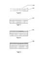
- a transparent substrate member 202 including a surface region 204is provided.
- the substrate membercan be a glass material such as soda lime glass in certain embodiment. Soda lime glass is a cost effective option for the transparent substrate member. Other suitable transparent substrates such as quartz, fused silica, solar glass can also be used.
- Each of the transparent substratecan include a barrier layer deposited on a surface region.
- the barrier layerprevents sodium ions from the glass material to diffuse into photovoltaic material area in a specific embodiment.
- the barrier layercan be a dielectric material such as silicon oxide deposited using technique such as a sputtering process, a chemical vapor deposition process, including plasma enhanced processes, and others. Other barrier materials may also be used. These barrier materials include aluminum oxide, titanium nitride, silicon nitride, tantalum oxide, zirconium oxide depending on the embodiment.
- the methodincludes forming a first electrode layer 302 overlying the surface region of the transparent substrate member which can have a barrier layer formed thereon.
- the first electrode layermay be provided using a transparent conductor oxide (TCO) such as indium tin oxide (commonly called ITO), fluorine doped tin oxide, and the like.
- TCOtransparent conductor oxide
- ITOindium tin oxide
- fluorine doped tin oxideand the like.
- the first electrode layermay be provided using a metal material.
- the metal materialcan be a molybdenum material in a specific embodiment.
- the molybdenum materialcan be formed using deposition techniques such as sputtering, plating, physical vapor deposition (including evaporation, sublimation), chemical vapor deposition (including plasma enhanced processes) following by a patterning process.
- Molybdenum materialprovides certain advantage over other electrode material for a CIG or CIGS based thin film photovoltaic cells.
- molybdenum materialprovides a low contact resistance for CIGS film and stability over subsequent process steps.
- molybdenum materialis formed by depositing a first molybdenum layer overlying the transparent substrate member.
- the first molybdenum layerhas a first thickness and a tensile characteristics in a specific embodiment.
- a second molybdenum layer having a compression characteristics and a second thicknessis formed overlying the first molybdenum layer.
- the first electrode layer comprising the molybdenum materialcan be further patterned as shown.
- the methodincludes forming an absorber layer 402 overlying a surface region of the first electrode layer.
- the absorber layercan be a thin film semiconductor material in a specific embodiment.
- the thin film semiconductor materialis a p-type semiconductor material provided by a copper indium disulfide material, or a copper indium gallium disulfide material, or a copper indium diselenide material, or a copper indium gallium diselenide material, any combination of these, or others, depending on the application.
- the p-type characteristicsmay be provided using dopants such as boron or aluminum species.
- the absorber layermay be deposited by techniques such as sputtering, plating, evaporation including a sulfurization or selenization step. Further details of the formation of the absorber material may be found in Provisional U.S. Patent Application No. 61/059,253, titled “High Efficiency Photovoltaic Cell and Manufacturing Method,” commonly assigned, and hereby incorporated by reference.
- the methodforms a window layer 502 overlying a surface region of the absorber layer to form a photovoltaic film stack to provide for a pn junction for the photovoltaic cell.
- the window layeris often provided using a wide bandgap n-type semiconductor material for a p-type absorber layer in a specific embodiment.
- the window layeruses a cadmium sulfide material for a photovoltaic cell using CIGS, CIS and related materials as absorber layer.
- the window layercan be deposited using techniques such as sputtering, vacuum evaporation, chemical bath deposition, among others.
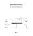
- the methodincludes providing a substrate 602 .
- the substrateincludes a transparent substrate member having a first electrode layer overlying the transparent substrate member.
- a thin film absorber layeroverlies the first electrode layer and a window layer overlies the thin film absorber layer.
- the substrateis loaded into a chamber 604 .
- the chamberincludes an internal volume 606 .
- the chamberalso includes pumping system 608 to provide a suitable vacuum level.
- the chamberincludes one or more gas lines 610 and various auxiliaries to introduce one or more precursor species for forming a transparent conductive oxide material 614 overlying the window layer in a specific embodiment.
- the chamberincludes one or more heating devices 612 to provide a suitable reaction temperature for the deposition of the transparent conductive material.
- the transparent conductive oxideincludes a zinc oxide material.
- the methodincludes loading the substrate into the chamber.
- the chamber together with the substrateis pumped down to a pressure ranging from about 0.1 torr to about 0.02 torr in a specific embodiment.
- a mixture of reactant or precursor speciesis introduced into the chamber using the one or more gas lines.
- the mixture of reactant speciescan include a diethyl zinc material and a oxygen bearing species provided using a carrier gas.
- the oxygen bearing speciescan be water in a specific embodiment.
- the diethyl zinc materialmay be provide as a semiconductor grade, or a catalyst grade depending on the embodiment. In a specific embodiment, the water to diethylzinc ratio is greater than about 1 to about 4.
- the water to diethylzinc ratiois about 1.
- the carrier gascan be inert gases such as nitrogen, argon , helium, and the like.
- a boron bearing species derived from a diborane speciesmay also be introduced at a selected flow rate together with the mixture of reactants to form a boron doped zinc oxide material.
- Other boron bearing speciessuch as boron halides (for example, boron trichloride, boron trifluoride, boron tribromide), or boron hydrohalides may also be used depending on the application.
- the diborane speciesis provided at a diborane to diethylzinc ratio of zero percent to about five percent.
- the diborane ratio to diethylzinc ratiois about one percent.
- the chambercan be at a pressure of about 0.5 torr to about 1 torr during deposition of the zinc oxide material.
- the substrateis maintain at a temperature ranging from about 130 Degree Celsius to about 190 Degree Celsius for the deposition of the zinc oxide material. In an alternative embodiment, the substrate is maintained at a temperature of about 200 Degree Celsius and may be higher.
- the boron bearing speciesreduce a resistivity characteristic of the zinc oxide material. Depending on a level of the boron bearing species in the zinc oxide material, the zinc oxide material can have a resistivity of about 2.5 milliohm-cm and less.
- the zinc oxide materialcan have a grain size ranging from about 3000 Angstroms to about 5000 Angstroms to provide a transmission rate of 80 percent or greater and preferably 90 percent and greater for electromagnetic radiation in a wavelength range ranging from about 800 nanometers to about 1200 nanometers.
- the zinc oxide materialcan have a hazy appearance in a specific embodiment. Of course there can be other variations, modifications, and alternatives.
- the zinc oxide materialis illustrated using boron as a dopant species.
- Other dopantssuch as hydrogen, aluminum, indium, gallium, and the likes may also be used.
- the abovehas been generally described in terms of a specific structure for CIS and/or CIGS thin film cells, other specific CIS and/or CIGS configurations can also be used, such as those noted in U.S. Pat. Nos.
Landscapes
- Engineering & Computer Science (AREA)
- Microelectronics & Electronic Packaging (AREA)
- Power Engineering (AREA)
- Physics & Mathematics (AREA)
- Condensed Matter Physics & Semiconductors (AREA)
- General Physics & Mathematics (AREA)
- Manufacturing & Machinery (AREA)
- Computer Hardware Design (AREA)
- Chemical & Material Sciences (AREA)
- Materials Engineering (AREA)
- General Chemical & Material Sciences (AREA)
- Inorganic Chemistry (AREA)
- Chemical Kinetics & Catalysis (AREA)
- Mechanical Engineering (AREA)
- Metallurgy (AREA)
- Organic Chemistry (AREA)
- Photovoltaic Devices (AREA)
- Life Sciences & Earth Sciences (AREA)
- Sustainable Energy (AREA)
Abstract
Description
Claims (18)
Priority Applications (1)
| Application Number | Priority Date | Filing Date | Title |
|---|---|---|---|
| US14/025,592US9059370B2 (en) | 2008-10-17 | 2013-09-12 | Zinc oxide film method and structure for CIGS cell |
Applications Claiming Priority (4)
| Application Number | Priority Date | Filing Date | Title |
|---|---|---|---|
| US10615808P | 2008-10-17 | 2008-10-17 | |
| US12/577,132US8168463B2 (en) | 2008-10-17 | 2009-10-09 | Zinc oxide film method and structure for CIGS cell |
| US13/371,239US8557625B1 (en) | 2008-10-17 | 2012-02-10 | Zinc oxide film method and structure for cigs cell |
| US14/025,592US9059370B2 (en) | 2008-10-17 | 2013-09-12 | Zinc oxide film method and structure for CIGS cell |
Related Parent Applications (1)
| Application Number | Title | Priority Date | Filing Date |
|---|---|---|---|
| US13/371,239ContinuationUS8557625B1 (en) | 2008-10-17 | 2012-02-10 | Zinc oxide film method and structure for cigs cell |
Publications (2)
| Publication Number | Publication Date |
|---|---|
| US20140170808A1 US20140170808A1 (en) | 2014-06-19 |
| US9059370B2true US9059370B2 (en) | 2015-06-16 |
Family
ID=43558390
Family Applications (3)
| Application Number | Title | Priority Date | Filing Date |
|---|---|---|---|
| US12/577,132Expired - Fee RelatedUS8168463B2 (en) | 2008-10-17 | 2009-10-09 | Zinc oxide film method and structure for CIGS cell |
| US13/371,239Expired - Fee RelatedUS8557625B1 (en) | 2008-10-17 | 2012-02-10 | Zinc oxide film method and structure for cigs cell |
| US14/025,592Expired - Fee RelatedUS9059370B2 (en) | 2008-10-17 | 2013-09-12 | Zinc oxide film method and structure for CIGS cell |
Family Applications Before (2)
| Application Number | Title | Priority Date | Filing Date |
|---|---|---|---|
| US12/577,132Expired - Fee RelatedUS8168463B2 (en) | 2008-10-17 | 2009-10-09 | Zinc oxide film method and structure for CIGS cell |
| US13/371,239Expired - Fee RelatedUS8557625B1 (en) | 2008-10-17 | 2012-02-10 | Zinc oxide film method and structure for cigs cell |
Country Status (4)
| Country | Link |
|---|---|
| US (3) | US8168463B2 (en) |
| EP (1) | EP2309554A3 (en) |
| CN (1) | CN102044632B (en) |
| TW (1) | TWI501414B (en) |
Families Citing this family (29)
| Publication number | Priority date | Publication date | Assignee | Title |
|---|---|---|---|---|
| US9105776B2 (en)* | 2006-05-15 | 2015-08-11 | Stion Corporation | Method and structure for thin film photovoltaic materials using semiconductor materials |
| US8071179B2 (en) | 2007-06-29 | 2011-12-06 | Stion Corporation | Methods for infusing one or more materials into nano-voids if nanoporous or nanostructured materials |
| US8759671B2 (en) | 2007-09-28 | 2014-06-24 | Stion Corporation | Thin film metal oxide bearing semiconductor material for single junction solar cell devices |
| US7998762B1 (en) | 2007-11-14 | 2011-08-16 | Stion Corporation | Method and system for large scale manufacture of thin film photovoltaic devices using multi-chamber configuration |
| US8772078B1 (en) | 2008-03-03 | 2014-07-08 | Stion Corporation | Method and system for laser separation for exclusion region of multi-junction photovoltaic materials |
| US8642138B2 (en)* | 2008-06-11 | 2014-02-04 | Stion Corporation | Processing method for cleaning sulfur entities of contact regions |
| US9087943B2 (en) | 2008-06-25 | 2015-07-21 | Stion Corporation | High efficiency photovoltaic cell and manufacturing method free of metal disulfide barrier material |
| US8003432B2 (en) | 2008-06-25 | 2011-08-23 | Stion Corporation | Consumable adhesive layer for thin film photovoltaic material |
| US7855089B2 (en) | 2008-09-10 | 2010-12-21 | Stion Corporation | Application specific solar cell and method for manufacture using thin film photovoltaic materials |
| US7863074B2 (en) | 2008-09-30 | 2011-01-04 | Stion Corporation | Patterning electrode materials free from berm structures for thin film photovoltaic cells |
| US7947524B2 (en) | 2008-09-30 | 2011-05-24 | Stion Corporation | Humidity control and method for thin film photovoltaic materials |
| US8425739B1 (en) | 2008-09-30 | 2013-04-23 | Stion Corporation | In chamber sodium doping process and system for large scale cigs based thin film photovoltaic materials |
| US8383450B2 (en) | 2008-09-30 | 2013-02-26 | Stion Corporation | Large scale chemical bath system and method for cadmium sulfide processing of thin film photovoltaic materials |
| US8741689B2 (en) | 2008-10-01 | 2014-06-03 | Stion Corporation | Thermal pre-treatment process for soda lime glass substrate for thin film photovoltaic materials |
| US8168463B2 (en) | 2008-10-17 | 2012-05-01 | Stion Corporation | Zinc oxide film method and structure for CIGS cell |
| US8344243B2 (en) | 2008-11-20 | 2013-01-01 | Stion Corporation | Method and structure for thin film photovoltaic cell using similar material junction |
| US8507786B1 (en) | 2009-06-27 | 2013-08-13 | Stion Corporation | Manufacturing method for patterning CIGS/CIS solar cells |
| US8398772B1 (en) | 2009-08-18 | 2013-03-19 | Stion Corporation | Method and structure for processing thin film PV cells with improved temperature uniformity |
| US8809096B1 (en) | 2009-10-22 | 2014-08-19 | Stion Corporation | Bell jar extraction tool method and apparatus for thin film photovoltaic materials |
| US8859880B2 (en) | 2010-01-22 | 2014-10-14 | Stion Corporation | Method and structure for tiling industrial thin-film solar devices |
| US9096930B2 (en) | 2010-03-29 | 2015-08-04 | Stion Corporation | Apparatus for manufacturing thin film photovoltaic devices |
| US8461061B2 (en) | 2010-07-23 | 2013-06-11 | Stion Corporation | Quartz boat method and apparatus for thin film thermal treatment |
| US8628997B2 (en)* | 2010-10-01 | 2014-01-14 | Stion Corporation | Method and device for cadmium-free solar cells |
| US8906732B2 (en)* | 2010-10-01 | 2014-12-09 | Stion Corporation | Method and device for cadmium-free solar cells |
| US8728200B1 (en)* | 2011-01-14 | 2014-05-20 | Stion Corporation | Method and system for recycling processing gas for selenization of thin film photovoltaic materials |
| US8998606B2 (en) | 2011-01-14 | 2015-04-07 | Stion Corporation | Apparatus and method utilizing forced convection for uniform thermal treatment of thin film devices |
| US8436445B2 (en) | 2011-08-15 | 2013-05-07 | Stion Corporation | Method of manufacture of sodium doped CIGS/CIGSS absorber layers for high efficiency photovoltaic devices |
| CN102597858A (en)* | 2011-11-29 | 2012-07-18 | 深圳市华星光电技术有限公司 | Liquid crystal panel, OLED display panel, glass substrate and manufacturing method thereof |
| CN105047750A (en)* | 2014-10-10 | 2015-11-11 | 广东汉能薄膜太阳能有限公司 | Method for increasing conversion efficiency of thin-film solar cell |
Citations (7)
| Publication number | Priority date | Publication date | Assignee | Title |
|---|---|---|---|---|
| US5699035A (en)* | 1991-12-13 | 1997-12-16 | Symetrix Corporation | ZnO thin-film varistors and method of making the same |
| US20030129307A1 (en)* | 2002-01-04 | 2003-07-10 | Rutgers, The State University Of New Jersey | Tailoring piezoelectric properties using MgxZn1-xO/ZnO material and MgxZn1-xO/ZnO structures |
| US20030232500A1 (en)* | 2000-12-07 | 2003-12-18 | Agarwal Vishnu K. | Photo-assisted method for semiconductor fabrication |
| US20060134347A1 (en)* | 2004-12-20 | 2006-06-22 | Shivkumar Chiruvolu | Dense coating formation by reactive deposition |
| JP2008172244A (en)* | 2007-01-09 | 2008-07-24 | Korea Electronics Telecommun | Method for forming ZnO semiconductor film for electronic device and thin film transistor including the semiconductor film |
| US20080241590A1 (en)* | 2007-03-30 | 2008-10-02 | Seoul Semiconductor Co., Ltd. | Method of coating sulfide phosphor and light emitting device employing coated sulfide phosphor |
| US20090091033A1 (en)* | 2005-05-27 | 2009-04-09 | Wei Gao | Fabrication of metal oxide films |
Family Cites Families (245)
| Publication number | Priority date | Publication date | Assignee | Title |
|---|---|---|---|---|
| US3520732A (en) | 1965-10-22 | 1970-07-14 | Matsushita Electric Industrial Co Ltd | Photovoltaic cell and process of preparation of same |
| US3828722A (en) | 1970-05-01 | 1974-08-13 | Cogar Corp | Apparatus for producing ion-free insulating layers |
| US3975211A (en) | 1975-03-28 | 1976-08-17 | Westinghouse Electric Corporation | Solar cells and method for making same |
| US4062038A (en) | 1976-01-28 | 1977-12-06 | International Business Machines Corporation | Radiation responsive device |
| US4332974A (en) | 1979-06-28 | 1982-06-01 | Chevron Research Company | Multilayer photovoltaic cell |
| US4263336A (en) | 1979-11-23 | 1981-04-21 | Motorola, Inc. | Reduced pressure induction heated reactor and method |
| EP0191503A3 (en) | 1980-04-10 | 1986-09-10 | Massachusetts Institute Of Technology | Method of producing sheets of crystalline material |
| US5217564A (en) | 1980-04-10 | 1993-06-08 | Massachusetts Institute Of Technology | Method of producing sheets of crystalline material and devices made therefrom |
| US4335266A (en) | 1980-12-31 | 1982-06-15 | The Boeing Company | Methods for forming thin-film heterojunction solar cells from I-III-VI.sub.2 |
| US4441113A (en) | 1981-02-13 | 1984-04-03 | Energy Conversion Devices, Inc. | P-Type semiconductor material having a wide band gap |
| US4465575A (en) | 1981-09-21 | 1984-08-14 | Atlantic Richfield Company | Method for forming photovoltaic cells employing multinary semiconductor films |
| DE3314197A1 (en) | 1982-04-28 | 1983-11-03 | Energy Conversion Devices, Inc., 48084 Troy, Mich. | P-CONDUCTING AMORPHOUS SILICON ALLOY WITH A LARGE BAND GAP AND MANUFACTURING PROCESS THEREFOR |
| US4442310A (en) | 1982-07-15 | 1984-04-10 | Rca Corporation | Photodetector having enhanced back reflection |
| US4518855A (en) | 1982-09-30 | 1985-05-21 | Spring-Mornne, Inc. | Method and apparatus for statically aligning shafts and monitoring shaft alignment |
| US4461922A (en) | 1983-02-14 | 1984-07-24 | Atlantic Richfield Company | Solar cell module |
| US4471155A (en) | 1983-04-15 | 1984-09-11 | Energy Conversion Devices, Inc. | Narrow band gap photovoltaic devices with enhanced open circuit voltage |
| US4724011A (en) | 1983-05-16 | 1988-02-09 | Atlantic Richfield Company | Solar cell interconnection by discrete conductive regions |
| US4517403A (en) | 1983-05-16 | 1985-05-14 | Atlantic Richfield Company | Series connected solar cells and method of formation |
| US4598306A (en) | 1983-07-28 | 1986-07-01 | Energy Conversion Devices, Inc. | Barrier layer for photovoltaic devices |
| US4532372A (en) | 1983-12-23 | 1985-07-30 | Energy Conversion Devices, Inc. | Barrier layer for photovoltaic devices |
| US4499658A (en) | 1983-09-06 | 1985-02-19 | Atlantic Richfield Company | Solar cell laminates |
| US4589194A (en) | 1983-12-29 | 1986-05-20 | Atlantic Richfield Company | Ultrasonic scribing of thin film solar cells |
| US4542255A (en) | 1984-01-03 | 1985-09-17 | Atlantic Richfield Company | Gridded thin film solar cell |
| US4581108A (en) | 1984-01-06 | 1986-04-08 | Atlantic Richfield Company | Process of forming a compound semiconductive material |
| US4661370A (en) | 1984-02-08 | 1987-04-28 | Atlantic Richfield Company | Electric discharge processing of thin films |
| US4507181A (en) | 1984-02-17 | 1985-03-26 | Energy Conversion Devices, Inc. | Method of electro-coating a semiconductor device |
| US4611091A (en) | 1984-12-06 | 1986-09-09 | Atlantic Richfield Company | CuInSe2 thin film solar cell with thin CdS and transparent window layer |
| US4599154A (en) | 1985-03-15 | 1986-07-08 | Atlantic Richfield Company | Electrically enhanced liquid jet processing |
| US4663495A (en) | 1985-06-04 | 1987-05-05 | Atlantic Richfield Company | Transparent photovoltaic module |
| US4612411A (en) | 1985-06-04 | 1986-09-16 | Atlantic Richfield Company | Thin film solar cell with ZnO window layer |
| US4638111A (en) | 1985-06-04 | 1987-01-20 | Atlantic Richfield Company | Thin film solar cell module |
| US4623601A (en) | 1985-06-04 | 1986-11-18 | Atlantic Richfield Company | Photoconductive device containing zinc oxide transparent conductive layer |
| JPH0682625B2 (en) | 1985-06-04 | 1994-10-19 | シーメンス ソーラー インダストリーズ,エル.ピー. | Deposition method of zinc oxide film |
| US4798660A (en) | 1985-07-16 | 1989-01-17 | Atlantic Richfield Company | Method for forming Cu In Se2 films |
| US4625070A (en) | 1985-08-30 | 1986-11-25 | Atlantic Richfield Company | Laminated thin film solar module |
| JPS6273784A (en) | 1985-09-27 | 1987-04-04 | Sanyo Electric Co Ltd | photovoltaic device |
| US4865999A (en) | 1987-07-08 | 1989-09-12 | Glasstech Solar, Inc. | Solar cell fabrication method |
| US4775425A (en) | 1987-07-27 | 1988-10-04 | Energy Conversion Devices, Inc. | P and n-type microcrystalline semiconductor alloy material including band gap widening elements, devices utilizing same |
| US4816082A (en) | 1987-08-19 | 1989-03-28 | Energy Conversion Devices, Inc. | Thin film solar cell including a spatially modulated intrinsic layer |
| US4968354A (en) | 1987-11-09 | 1990-11-06 | Fuji Electric Co., Ltd. | Thin film solar cell array |
| US5045409A (en) | 1987-11-27 | 1991-09-03 | Atlantic Richfield Company | Process for making thin film solar cell |
| US4793283A (en) | 1987-12-10 | 1988-12-27 | Sarkozy Robert F | Apparatus for chemical vapor deposition with clean effluent and improved product yield |
| US5008062A (en) | 1988-01-20 | 1991-04-16 | Siemens Solar Industries, L.P. | Method of fabricating photovoltaic module |
| US5259883A (en) | 1988-02-16 | 1993-11-09 | Kabushiki Kaisha Toshiba | Method of thermally processing semiconductor wafers and an apparatus therefor |
| US4915745A (en) | 1988-09-22 | 1990-04-10 | Atlantic Richfield Company | Thin film solar cell and method of making |
| US5180686A (en) | 1988-10-31 | 1993-01-19 | Energy Conversion Devices, Inc. | Method for continuously deposting a transparent oxide material by chemical pyrolysis |
| US4873118A (en)* | 1988-11-18 | 1989-10-10 | Atlantic Richfield Company | Oxygen glow treating of ZnO electrode for thin film silicon solar cell |
| US4996108A (en) | 1989-01-17 | 1991-02-26 | Simon Fraser University | Sheets of transition metal dichalcogenides |
| US4950615A (en) | 1989-02-06 | 1990-08-21 | International Solar Electric Technology, Inc. | Method and making group IIB metal - telluride films and solar cells |
| FR2646560B1 (en) | 1989-04-27 | 1994-01-14 | Solems Sa | METHOD FOR IMPROVING THE SPECTRAL RESPONSE OF AN IMPROVED PHOTOCONDUCTOR STRUCTURE, SOLAR CELL AND PHOTORECEPTIVE STRUCTURE |
| US5028274A (en) | 1989-06-07 | 1991-07-02 | International Solar Electric Technology, Inc. | Group I-III-VI2 semiconductor films for solar cell application |
| DE69024304T2 (en) | 1989-09-06 | 1996-07-18 | Sanyo Electric Co | Manufacturing process for a flexible photovoltaic device |
| US5078803A (en) | 1989-09-22 | 1992-01-07 | Siemens Solar Industries L.P. | Solar cells incorporating transparent electrodes comprising hazy zinc oxide |
| JPH03124067A (en) | 1989-10-07 | 1991-05-27 | Showa Shell Sekiyu Kk | Photovoltaic device and its manufacture |
| US5011565A (en) | 1989-12-06 | 1991-04-30 | Mobil Solar Energy Corporation | Dotted contact solar cell and method of making same |
| US5154777A (en) | 1990-02-26 | 1992-10-13 | Mcdonnell Douglas Corporation | Advanced survivable space solar power system |
| DK170189B1 (en) | 1990-05-30 | 1995-06-06 | Yakov Safir | Process for the manufacture of semiconductor components, as well as solar cells made therefrom |
| EP0460287A1 (en) | 1990-05-31 | 1991-12-11 | Siemens Aktiengesellschaft | Novel chalcopyrite solar cell |
| DE59009771D1 (en) | 1990-07-24 | 1995-11-16 | Siemens Ag | Process for the manufacture of a chalcopyrite solar cell. |
| JP2729239B2 (en) | 1990-10-17 | 1998-03-18 | 昭和シェル石油株式会社 | Integrated photovoltaic device |
| US5528397A (en) | 1991-12-03 | 1996-06-18 | Kopin Corporation | Single crystal silicon transistors for display panels |
| US6784492B1 (en) | 1991-03-18 | 2004-08-31 | Canon Kabushiki Kaisha | Semiconductor device including a gate-insulated transistor |
| JPH0788063A (en) | 1991-05-08 | 1995-04-04 | Sharp Corp | Handle mounting structure |
| US5211824A (en) | 1991-10-31 | 1993-05-18 | Siemens Solar Industries L.P. | Method and apparatus for sputtering of a liquid |
| US5231047A (en) | 1991-12-19 | 1993-07-27 | Energy Conversion Devices, Inc. | High quality photovoltaic semiconductor material and laser ablation method of fabrication same |
| US5501744A (en) | 1992-01-13 | 1996-03-26 | Photon Energy, Inc. | Photovoltaic cell having a p-type polycrystalline layer with large crystals |
| US5261968A (en) | 1992-01-13 | 1993-11-16 | Photon Energy, Inc. | Photovoltaic cell and method |
| JPH05243596A (en) | 1992-03-02 | 1993-09-21 | Showa Shell Sekiyu Kk | Manufacture of laminated type solar cell |
| WO1993019491A1 (en) | 1992-03-19 | 1993-09-30 | Siemens Solar Gmbh | Weather-resistant thin layer solar module |
| US5248349A (en) | 1992-05-12 | 1993-09-28 | Solar Cells, Inc. | Process for making photovoltaic devices and resultant product |
| US5298086A (en) | 1992-05-15 | 1994-03-29 | United Solar Systems Corporation | Method for the manufacture of improved efficiency tandem photovoltaic device and device manufactured thereby |
| EP0574716B1 (en) | 1992-05-19 | 1996-08-21 | Matsushita Electric Industrial Co., Ltd. | Method for preparing chalcopyrite-type compound |
| ATE170669T1 (en) | 1992-06-29 | 1998-09-15 | Canon Kk | RESIN COMPOSITION FOR SEALING AND A SEMICONDUCTOR DEVICE COVERED WITH SEALING RESIN COMPOSITION |
| EP0648373B1 (en) | 1992-06-29 | 2002-01-30 | United Solar Systems Corporation | Microwave energized deposition process with substrate temperature control |
| US5578503A (en) | 1992-09-22 | 1996-11-26 | Siemens Aktiengesellschaft | Rapid process for producing a chalcopyrite semiconductor on a substrate |
| US5474939A (en) | 1992-12-30 | 1995-12-12 | Siemens Solar Industries International | Method of making thin film heterojunction solar cell |
| US5436204A (en) | 1993-04-12 | 1995-07-25 | Midwest Research Institute | Recrystallization method to selenization of thin-film Cu(In,Ga)Se2 for semiconductor device applications |
| DE4333407C1 (en) | 1993-09-30 | 1994-11-17 | Siemens Ag | Solar cell comprising a chalcopyrite absorber layer |
| US5738731A (en) | 1993-11-19 | 1998-04-14 | Mega Chips Corporation | Photovoltaic device |
| EP0658924B1 (en) | 1993-12-17 | 2000-07-12 | Canon Kabushiki Kaisha | Method of manufacturing electron-emitting device, electron source and image-forming apparatus |
| CN1274009C (en) | 1994-06-15 | 2006-09-06 | 精工爱普生株式会社 | Method for making thin-film semicondcutor device |
| US5578103A (en) | 1994-08-17 | 1996-11-26 | Corning Incorporated | Alkali metal ion migration control |
| DE4442824C1 (en) | 1994-12-01 | 1996-01-25 | Siemens Ag | Solar cell having higher degree of activity |
| EP0729189A1 (en) | 1995-02-21 | 1996-08-28 | Interuniversitair Micro-Elektronica Centrum Vzw | Method of preparing solar cells and products obtained thereof |
| US5674325A (en) | 1995-06-07 | 1997-10-07 | Photon Energy, Inc. | Thin film photovoltaic device and process of manufacture |
| US6743723B2 (en) | 1995-09-14 | 2004-06-01 | Canon Kabushiki Kaisha | Method for fabricating semiconductor device |
| US5925308A (en) | 1996-08-05 | 1999-07-20 | Corning Incorporated | Rapid-setting formable mixtures and method of making and using same |
| US5977476A (en) | 1996-10-16 | 1999-11-02 | United Solar Systems Corporation | High efficiency photovoltaic device |
| JP3249408B2 (en) | 1996-10-25 | 2002-01-21 | 昭和シェル石油株式会社 | Method and apparatus for manufacturing thin film light absorbing layer of thin film solar cell |
| JP3249407B2 (en) | 1996-10-25 | 2002-01-21 | 昭和シェル石油株式会社 | Thin-film solar cells composed of chalcopyrite-based multi-compound semiconductor thin-film light-absorbing layers |
| JP3527815B2 (en) | 1996-11-08 | 2004-05-17 | 昭和シェル石油株式会社 | Method for producing transparent conductive film of thin film solar cell |
| US5985691A (en)* | 1997-05-16 | 1999-11-16 | International Solar Electric Technology, Inc. | Method of making compound semiconductor films and making related electronic devices |
| JPH1154773A (en) | 1997-08-01 | 1999-02-26 | Canon Inc | Photovoltaic element and method for manufacturing the same |
| DE19741832A1 (en) | 1997-09-23 | 1999-03-25 | Inst Solarenergieforschung | Method of manufacturing a solar cell and solar cell |
| US6258620B1 (en) | 1997-10-15 | 2001-07-10 | University Of South Florida | Method of manufacturing CIGS photovoltaic devices |
| JP2001523049A (en) | 1997-11-10 | 2001-11-20 | スターメガ コーポレイション | Quantum ridges and quantum peaks |
| DE69911529T2 (en) | 1998-02-05 | 2004-08-05 | Nippon Sheet Glass Co., Ltd. | OBJECT WITH A LEVEL SURFACE, METHOD FOR THE PRODUCTION THEREOF AND COMPILATION THEREFOR |
| US6107562A (en) | 1998-03-24 | 2000-08-22 | Matsushita Electric Industrial Co., Ltd. | Semiconductor thin film, method for manufacturing the same, and solar cell using the same |
| JPH11330507A (en)* | 1998-05-12 | 1999-11-30 | Yazaki Corp | Solar cell |
| US6344608B2 (en) | 1998-06-30 | 2002-02-05 | Canon Kabushiki Kaisha | Photovoltaic element |
| US6127202A (en) | 1998-07-02 | 2000-10-03 | International Solar Electronic Technology, Inc. | Oxide-based method of making compound semiconductor films and making related electronic devices |
| US6451415B1 (en) | 1998-08-19 | 2002-09-17 | The Trustees Of Princeton University | Organic photosensitive optoelectronic device with an exciton blocking layer |
| JP3428931B2 (en) | 1998-09-09 | 2003-07-22 | キヤノン株式会社 | Flat panel display dismantling method |
| US6323417B1 (en) | 1998-09-29 | 2001-11-27 | Lockheed Martin Corporation | Method of making I-III-VI semiconductor materials for use in photovoltaic cells |
| JP2000150861A (en) | 1998-11-16 | 2000-05-30 | Tdk Corp | Oxide thin film |
| JP3667178B2 (en) | 1998-11-24 | 2005-07-06 | キヤノン株式会社 | Method for producing zinc oxide thin film, method for producing photovoltaic element using the same, and photovoltaic element |
| JP2000173969A (en) | 1998-12-03 | 2000-06-23 | Canon Inc | Rinse method and photovoltaic device |
| JP2001156321A (en) | 1999-03-09 | 2001-06-08 | Fuji Xerox Co Ltd | Semiconductor device and method of manufacturing the same |
| US6160215A (en) | 1999-03-26 | 2000-12-12 | Curtin; Lawrence F. | Method of making photovoltaic device |
| US6307148B1 (en) | 1999-03-29 | 2001-10-23 | Shinko Electric Industries Co., Ltd. | Compound semiconductor solar cell and production method thereof |
| US6328871B1 (en) | 1999-08-16 | 2001-12-11 | Applied Materials, Inc. | Barrier layer for electroplating processes |
| WO2001057932A1 (en) | 2000-02-07 | 2001-08-09 | Cis Solartechnik Gmbh | Flexible metal substrate for cis solar cells, and method for producing the same |
| US6372538B1 (en) | 2000-03-16 | 2002-04-16 | University Of Delaware | Fabrication of thin-film, flexible photovoltaic module |
| US7194197B1 (en) | 2000-03-16 | 2007-03-20 | Global Solar Energy, Inc. | Nozzle-based, vapor-phase, plume delivery structure for use in production of thin-film deposition layer |
| US7414188B2 (en) | 2002-01-25 | 2008-08-19 | Konarka Technologies, Inc. | Co-sensitizers for dye sensitized solar cells |
| US6423565B1 (en) | 2000-05-30 | 2002-07-23 | Kurt L. Barth | Apparatus and processes for the massproduction of photovotaic modules |
| CN101798057A (en) | 2000-08-22 | 2010-08-11 | 哈佛学院董事会 | Doped elongated semiconductors, growing such semiconductors, devices including such semiconductors and fabricating such devices |
| US7301199B2 (en) | 2000-08-22 | 2007-11-27 | President And Fellows Of Harvard College | Nanoscale wires and related devices |
| JP2002196337A (en) | 2000-09-06 | 2002-07-12 | Seiko Epson Corp | Method and apparatus for manufacturing electro-optical device, and method and apparatus for manufacturing liquid crystal panel |
| JP2002167695A (en) | 2000-09-19 | 2002-06-11 | Canon Inc | Method for forming zinc oxide film and method for manufacturing photovoltaic element using the same |
| US6576112B2 (en) | 2000-09-19 | 2003-06-10 | Canon Kabushiki Kaisha | Method of forming zinc oxide film and process for producing photovoltaic device using it |
| DE10104726A1 (en) | 2001-02-02 | 2002-08-08 | Siemens Solar Gmbh | Process for structuring an oxide layer applied to a carrier material |
| JP4827303B2 (en) | 2001-03-12 | 2011-11-30 | キヤノン株式会社 | Photovoltaic element, TFT, and method for forming i-type semiconductor layer |
| US6858308B2 (en) | 2001-03-12 | 2005-02-22 | Canon Kabushiki Kaisha | Semiconductor element, and method of forming silicon-based film |
| JP2002299670A (en) | 2001-04-03 | 2002-10-11 | Canon Inc | Silicon based thin film and photovoltaic device |
| US7842882B2 (en) | 2004-03-01 | 2010-11-30 | Basol Bulent M | Low cost and high throughput deposition methods and apparatus for high density semiconductor film growth |
| US7053294B2 (en) | 2001-07-13 | 2006-05-30 | Midwest Research Institute | Thin-film solar cell fabricated on a flexible metallic substrate |
| JP2003106895A (en)* | 2001-10-01 | 2003-04-09 | Nec Corp | Thermal infrared detecting element and method of manufacturing the same |
| JP4236081B2 (en) | 2001-10-16 | 2009-03-11 | 大日本印刷株式会社 | Method for producing pattern forming body |
| EP1443527A4 (en) | 2001-10-19 | 2007-09-12 | Asahi Glass Co Ltd | TRANSPARENT CONDUCTIVE OXIDE LAYER SUBSTRATE, PROCESS FOR PRODUCING THE SAME, AND PHOTOELECTRIC CONVERSION ELEMENT |
| US6635307B2 (en) | 2001-12-12 | 2003-10-21 | Nanotek Instruments, Inc. | Manufacturing method for thin-film solar cells |
| US7276749B2 (en) | 2002-02-05 | 2007-10-02 | E-Phocus, Inc. | Image sensor with microcrystalline germanium photodiode layer |
| US6690041B2 (en) | 2002-05-14 | 2004-02-10 | Global Solar Energy, Inc. | Monolithically integrated diodes in thin-film photovoltaic devices |
| US7560641B2 (en) | 2002-06-17 | 2009-07-14 | Shalini Menezes | Thin film solar cell configuration and fabrication method |
| US7291782B2 (en) | 2002-06-22 | 2007-11-06 | Nanosolar, Inc. | Optoelectronic device and fabrication method |
| US6852920B2 (en) | 2002-06-22 | 2005-02-08 | Nanosolar, Inc. | Nano-architected/assembled solar electricity cell |
| TW200425530A (en) | 2002-09-05 | 2004-11-16 | Nanosys Inc | Nanostructure and nanocomposite based compositions and photovoltaic devices |
| WO2004022637A2 (en) | 2002-09-05 | 2004-03-18 | Nanosys, Inc. | Nanocomposites |
| EP1556902A4 (en) | 2002-09-30 | 2009-07-29 | Miasole | APPARATUS AND METHOD FOR MANUFACTURING CON CURRENT FOR LARGE SCALE PRODUCTION OF THIN FILM SOLAR CELLS |
| US6849798B2 (en) | 2002-12-17 | 2005-02-01 | General Electric Company | Photovoltaic cell using stable Cu2O nanocrystals and conductive polymers |
| US6936761B2 (en) | 2003-03-29 | 2005-08-30 | Nanosolar, Inc. | Transparent electrode, optoelectronic apparatus and devices |
| US7279832B2 (en) | 2003-04-01 | 2007-10-09 | Innovalight, Inc. | Phosphor materials and illumination devices made therefrom |
| US20040252488A1 (en) | 2003-04-01 | 2004-12-16 | Innovalight | Light-emitting ceiling tile |
| EP1619728A4 (en) | 2003-04-09 | 2006-08-09 | Matsushita Electric Industrial Co Ltd | SOLAR CELL |
| JP2004332043A (en) | 2003-05-07 | 2004-11-25 | Canon Inc | Method and apparatus for forming zinc oxide thin film, and method for forming photovoltaic element |
| US7462774B2 (en) | 2003-05-21 | 2008-12-09 | Nanosolar, Inc. | Photovoltaic devices fabricated from insulating nanostructured template |
| US7265037B2 (en) | 2003-06-20 | 2007-09-04 | The Regents Of The University Of California | Nanowire array and nanowire solar cells and methods for forming the same |
| KR100838805B1 (en) | 2003-07-14 | 2008-06-17 | 가부시키가이샤후지쿠라 | Electrolyte composition, photoelectric conversion element and dye-sensitized solar cell using same |
| KR101024288B1 (en) | 2003-07-24 | 2011-03-29 | 가부시키가이샤 가네카 | Silicon Thin Film Solar Cell |
| AU2003300775A1 (en) | 2003-09-03 | 2005-04-21 | Midwest Research Institute | Zno/cu(inga)se2 solar cells prepared by vapor phase zn doping |
| EP1521308A1 (en) | 2003-10-02 | 2005-04-06 | Scheuten Glasgroep | Ball or grain-shaped semiconductor element to be used in solar cells and method of production; method of production of a solar cell with said semiconductor element and solar cell |
| US20070163643A1 (en) | 2004-02-19 | 2007-07-19 | Nanosolar, Inc. | High-throughput printing of chalcogen layer and the use of an inter-metallic material |
| US8623448B2 (en) | 2004-02-19 | 2014-01-07 | Nanosolar, Inc. | High-throughput printing of semiconductor precursor layer from chalcogenide microflake particles |
| US20070169810A1 (en) | 2004-02-19 | 2007-07-26 | Nanosolar, Inc. | High-throughput printing of semiconductor precursor layer by use of chalcogen-containing vapor |
| JP4456107B2 (en) | 2004-02-20 | 2010-04-28 | シャープ株式会社 | Photoelectric conversion device and substrate for photoelectric conversion device |
| JP2005311292A (en) | 2004-03-25 | 2005-11-04 | Kaneka Corp | Substrate for thin film solar cell, manufacturing method therefor, and thin film solar cell using the same |
| US7122398B1 (en) | 2004-03-25 | 2006-10-17 | Nanosolar, Inc. | Manufacturing of optoelectronic devices |
| JP4695850B2 (en) | 2004-04-28 | 2011-06-08 | 本田技研工業株式会社 | Chalcopyrite solar cell |
| CN100463230C (en) | 2004-05-11 | 2009-02-18 | 本田技研工业株式会社 | Manufacturing method of chalcopyrite type thin film solar cell |
| TWI406890B (en) | 2004-06-08 | 2013-09-01 | Sandisk Corp | Post-deposition encapsulation of nanostructures : compositions, devices and systems incorporating same |
| EP1797584A4 (en) | 2004-06-08 | 2014-08-13 | Sandisk Corp | METHODS AND DEVICES FOR FORMING NANOSTRUCTURE MONOLAYERS AND DEVICES COMPRISING SUCH SINGLES |
| DE112005001429T5 (en) | 2004-06-18 | 2007-04-26 | Innovalight, Inc., St. Paul | Method and apparatus for forming nanoparticles using radio frequency plasmas |
| US7442320B2 (en) | 2004-06-18 | 2008-10-28 | Ultradots, Inc. | Nanostructured materials and photovoltaic devices including nanostructured materials |
| JP2006049768A (en) | 2004-08-09 | 2006-02-16 | Showa Shell Sekiyu Kk | CIS-based compound semiconductor thin film solar cell and method for producing light absorption layer of solar cell |
| US7750352B2 (en) | 2004-08-10 | 2010-07-06 | Pinion Technologies, Inc. | Light strips for lighting and backlighting applications |
| US7276724B2 (en) | 2005-01-20 | 2007-10-02 | Nanosolar, Inc. | Series interconnected optoelectronic device module assembly |
| US7732229B2 (en) | 2004-09-18 | 2010-06-08 | Nanosolar, Inc. | Formation of solar cells with conductive barrier layers and foil substrates |
| US20060249202A1 (en) | 2004-09-20 | 2006-11-09 | Seunghyup Yoo | Photovoltaic cell |
| WO2006053032A1 (en) | 2004-11-10 | 2006-05-18 | Daystar Technologies, Inc. | Thermal process for creation of an in-situ junction layer in cigs |
| US20060219288A1 (en) | 2004-11-10 | 2006-10-05 | Daystar Technologies, Inc. | Process and photovoltaic device using an akali-containing layer |
| CA2586970A1 (en) | 2004-11-10 | 2006-05-18 | Daystar Technologies, Inc. | Vertical production of photovoltaic devices |
| US20060096536A1 (en) | 2004-11-10 | 2006-05-11 | Daystar Technologies, Inc. | Pressure control system in a photovoltaic substrate deposition apparatus |
| CN101233260A (en) | 2004-11-10 | 2008-07-30 | 德斯塔尔科技公司 | Pressure control system in photovoltaic substrate deposition |
| US20060112983A1 (en) | 2004-11-17 | 2006-06-01 | Nanosys, Inc. | Photoactive devices and components with enhanced efficiency |
| US20060130890A1 (en) | 2004-12-20 | 2006-06-22 | Palo Alto Research Center Incorporated. | Heterojunction photovoltaic cell |
| JP2006179626A (en) | 2004-12-22 | 2006-07-06 | Showa Shell Sekiyu Kk | CIS-based thin-film solar cell module, method for producing the solar cell module, and separation method |
| JP4131965B2 (en) | 2004-12-28 | 2008-08-13 | 昭和シェル石油株式会社 | Method for producing light absorption layer of CIS thin film solar cell |
| JP2006183117A (en) | 2004-12-28 | 2006-07-13 | Showa Shell Sekiyu Kk | Manufacturing method of ZnO-based transparent conductive film by MOCVD (metal organic chemical vapor deposition) |
| JP2006186200A (en) | 2004-12-28 | 2006-07-13 | Showa Shell Sekiyu Kk | Precursor film and film forming method thereof |
| KR100495925B1 (en) | 2005-01-12 | 2005-06-17 | (주)인솔라텍 | Optical absorber layers for solar cell and manufacturing method thereof |
| JP5010806B2 (en) | 2005-02-01 | 2012-08-29 | 日本ペイント株式会社 | Powder coating composition and method for coating aluminum wheel |
| JP4801928B2 (en) | 2005-04-25 | 2011-10-26 | 富士フイルム株式会社 | Organic electroluminescence device |
| JP4841173B2 (en) | 2005-05-27 | 2011-12-21 | 昭和シェル石油株式会社 | High resistance buffer layer / window layer continuous film forming method and film forming apparatus for CIS thin film solar cell |
| JP3963924B2 (en) | 2005-07-22 | 2007-08-22 | 本田技研工業株式会社 | Chalcopyrite solar cell |
| WO2007019188A2 (en) | 2005-08-05 | 2007-02-15 | First Solar, Inc. | Manufacture of photovoltaic devices |
| FR2890232A1 (en) | 2005-08-23 | 2007-03-02 | Saint Gobain | COPLANAR DISCHARGE PLANE LAMP AND USES THEREFOR |
| JP2007123721A (en) | 2005-10-31 | 2007-05-17 | Rohm Co Ltd | Method for manufacturing photoelectric conversion device and photoelectric conversion device |
| US7442413B2 (en) | 2005-11-18 | 2008-10-28 | Daystar Technologies, Inc. | Methods and apparatus for treating a work piece with a vaporous element |
| EP1964180B1 (en)* | 2005-12-21 | 2010-08-04 | Saint-Gobain Glass France S.A. | Process of making a thin-film photovoltaic device |
| DE102005062977B3 (en) | 2005-12-28 | 2007-09-13 | Sulfurcell Solartechnik Gmbh | Method and apparatus for converting metallic precursor layers to chalcopyrite layers of CIGSS solar cells |
| US8389852B2 (en) | 2006-02-22 | 2013-03-05 | Guardian Industries Corp. | Electrode structure for use in electronic device and method of making same |
| US7235736B1 (en) | 2006-03-18 | 2007-06-26 | Solyndra, Inc. | Monolithic integration of cylindrical solar cells |
| US9105776B2 (en) | 2006-05-15 | 2015-08-11 | Stion Corporation | Method and structure for thin film photovoltaic materials using semiconductor materials |
| US8017860B2 (en) | 2006-05-15 | 2011-09-13 | Stion Corporation | Method and structure for thin film photovoltaic materials using bulk semiconductor materials |
| US8617640B2 (en) | 2006-06-12 | 2013-12-31 | Nanosolar, Inc. | Thin-film devices formed from solid group IIIA alloy particles |
| US7879685B2 (en) | 2006-08-04 | 2011-02-01 | Solyndra, Inc. | System and method for creating electric isolation between layers comprising solar cells |
| TW200810167A (en) | 2006-08-09 | 2008-02-16 | Ind Tech Res Inst | Dye-sensitized solar cell and the method of fabricating thereof |
| DE102006041046A1 (en) | 2006-09-01 | 2008-03-06 | Cis Solartechnik Gmbh & Co. Kg | Solar cell, process for the production of solar cells and electrical trace |
| US8426722B2 (en) | 2006-10-24 | 2013-04-23 | Zetta Research and Development LLC—AQT Series | Semiconductor grain and oxide layer for photovoltaic cells |
| US8203073B2 (en) | 2006-11-02 | 2012-06-19 | Guardian Industries Corp. | Front electrode for use in photovoltaic device and method of making same |
| FR2908406B1 (en) | 2006-11-14 | 2012-08-24 | Saint Gobain | POROUS LAYER, METHOD FOR MANUFACTURING THE SAME, AND APPLICATIONS THEREOF |
| US20080121264A1 (en) | 2006-11-28 | 2008-05-29 | Industrial Technology Research Institute | Thin film solar module and method of fabricating the same |
| MX2009006725A (en) | 2006-12-21 | 2009-06-30 | Helianthos Bv | METHOD FOR PREPARING SOLAR SUB-CELLS FROM A SOLAR CELL. |
| WO2008095146A2 (en) | 2007-01-31 | 2008-08-07 | Van Duren Jeroen K J | Solar cell absorber layer formed from metal ion precursors |
| US20080204696A1 (en) | 2007-02-28 | 2008-08-28 | Tdk Corporation | Method of alignment |
| KR100882668B1 (en) | 2007-07-18 | 2009-02-06 | 삼성모바일디스플레이주식회사 | Organic light emitting display device and manufacturing method thereof |
| FR2919429B1 (en) | 2007-07-27 | 2009-10-09 | Saint Gobain | FRONT PANEL SUBSTRATE OF PHOTOVOLTAIC CELL AND USE OF A SUBSTRATE FOR A FRONT PANEL OF PHOTOVOLTAIC CELL |
| US20090087939A1 (en) | 2007-09-28 | 2009-04-02 | Stion Corporation | Column structure thin film material using metal oxide bearing semiconductor material for solar cell devices |
| JP2009099476A (en) | 2007-10-19 | 2009-05-07 | Sony Corp | Dye-sensitized photoelectric conversion element and method for producing the same |
| US7998762B1 (en) | 2007-11-14 | 2011-08-16 | Stion Corporation | Method and system for large scale manufacture of thin film photovoltaic devices using multi-chamber configuration |
| JP2009135337A (en) | 2007-11-30 | 2009-06-18 | Showa Shell Sekiyu Kk | Laminated structure of CIS solar cell, integrated structure of CIS thin film solar cell, and manufacturing method |
| US8001283B2 (en) | 2008-03-12 | 2011-08-16 | Mips Technologies, Inc. | Efficient, scalable and high performance mechanism for handling IO requests |
| US8981211B2 (en) | 2008-03-18 | 2015-03-17 | Zetta Research and Development LLC—AQT Series | Interlayer design for epitaxial growth of semiconductor layers |
| US20090235987A1 (en) | 2008-03-24 | 2009-09-24 | Epv Solar, Inc. | Chemical Treatments to Enhance Photovoltaic Performance of CIGS |
| US20090255467A1 (en) | 2008-04-15 | 2009-10-15 | Global Solar Energy, Inc. | Apparatus and methods for manufacturing thin-film solar cells |
| JP4384237B2 (en) | 2008-05-19 | 2009-12-16 | 昭和シェル石油株式会社 | CIS type thin film solar cell manufacturing method |
| FR2932009B1 (en) | 2008-06-02 | 2010-09-17 | Saint Gobain | PHOTOVOLTAIC CELL AND PHOTOVOLTAIC CELL SUBSTRATE |
| CN101295586B (en)* | 2008-06-11 | 2012-05-30 | 中国科学院上海硅酸盐研究所 | A kind of fabrication method of nanocrystalline TiO2 solar cell prototype device |
| US8003432B2 (en) | 2008-06-25 | 2011-08-23 | Stion Corporation | Consumable adhesive layer for thin film photovoltaic material |
| US7855089B2 (en) | 2008-09-10 | 2010-12-21 | Stion Corporation | Application specific solar cell and method for manufacture using thin film photovoltaic materials |
| US8008112B1 (en) | 2008-09-29 | 2011-08-30 | Stion Corporation | Bulk chloride species treatment of thin film photovoltaic cell and manufacturing method |
| US8008111B1 (en) | 2008-09-29 | 2011-08-30 | Stion Corporation | Bulk copper species treatment of thin film photovoltaic cell and manufacturing method |
| US8008110B1 (en) | 2008-09-29 | 2011-08-30 | Stion Corporation | Bulk sodium species treatment of thin film photovoltaic cell and manufacturing method |
| US8053274B2 (en) | 2008-09-30 | 2011-11-08 | Stion Corporation | Self cleaning large scale method and furnace system for selenization of thin film photovoltaic materials |
| US8217261B2 (en) | 2008-09-30 | 2012-07-10 | Stion Corporation | Thin film sodium species barrier method and structure for cigs based thin film photovoltaic cell |
| US7863074B2 (en) | 2008-09-30 | 2011-01-04 | Stion Corporation | Patterning electrode materials free from berm structures for thin film photovoltaic cells |
| US7960204B2 (en) | 2008-09-30 | 2011-06-14 | Stion Corporation | Method and structure for adhesion of absorber material for thin film photovoltaic cell |
| US7947524B2 (en) | 2008-09-30 | 2011-05-24 | Stion Corporation | Humidity control and method for thin film photovoltaic materials |
| US7910399B1 (en) | 2008-09-30 | 2011-03-22 | Stion Corporation | Thermal management and method for large scale processing of CIS and/or CIGS based thin films overlying glass substrates |
| US8741689B2 (en) | 2008-10-01 | 2014-06-03 | Stion Corporation | Thermal pre-treatment process for soda lime glass substrate for thin film photovoltaic materials |
| US20110018103A1 (en) | 2008-10-02 | 2011-01-27 | Stion Corporation | System and method for transferring substrates in large scale processing of cigs and/or cis devices |
| US8003430B1 (en) | 2008-10-06 | 2011-08-23 | Stion Corporation | Sulfide species treatment of thin film photovoltaic cell and manufacturing method |
| US8168463B2 (en) | 2008-10-17 | 2012-05-01 | Stion Corporation | Zinc oxide film method and structure for CIGS cell |
| US8344243B2 (en) | 2008-11-20 | 2013-01-01 | Stion Corporation | Method and structure for thin film photovoltaic cell using similar material junction |
| US20100197051A1 (en) | 2009-02-04 | 2010-08-05 | Applied Materials, Inc. | Metrology and inspection suite for a solar production line |
| US8197912B2 (en) | 2009-03-12 | 2012-06-12 | International Business Machines Corporation | Precision separation of PV thin film stacks |
| US8859880B2 (en) | 2010-01-22 | 2014-10-14 | Stion Corporation | Method and structure for tiling industrial thin-film solar devices |
| US9096930B2 (en) | 2010-03-29 | 2015-08-04 | Stion Corporation | Apparatus for manufacturing thin film photovoltaic devices |
| US8142521B2 (en) | 2010-03-29 | 2012-03-27 | Stion Corporation | Large scale MOCVD system for thin film photovoltaic devices |
| US20110259395A1 (en) | 2010-04-21 | 2011-10-27 | Stion Corporation | Single Junction CIGS/CIS Solar Module |
| US20110259413A1 (en) | 2010-04-21 | 2011-10-27 | Stion Corporation | Hazy Zinc Oxide Film for Shaped CIGS/CIS Solar Cells |
| US20120018828A1 (en) | 2010-07-23 | 2012-01-26 | Stion Corporation | Sodium Sputtering Doping Method for Large Scale CIGS Based Thin Film Photovoltaic Materials |
| US8461061B2 (en) | 2010-07-23 | 2013-06-11 | Stion Corporation | Quartz boat method and apparatus for thin film thermal treatment |
| US9215235B1 (en) | 2011-05-23 | 2015-12-15 | Palo Alto Networks, Inc. | Using events to identify a user and enforce policies |
| FR3058855A1 (en) | 2016-11-16 | 2018-05-18 | Commissariat A L'energie Atomique Et Aux Energies Alternatives | SWITCH HAVING PHASE CHANGE MATERIAL |
- 2009
- 2009-10-09USUS12/577,132patent/US8168463B2/ennot_activeExpired - Fee Related
- 2010
- 2010-09-30TWTW099133467Apatent/TWI501414B/ennot_activeIP Right Cessation
- 2010-09-30CNCN201010503960.1Apatent/CN102044632B/ennot_activeExpired - Fee Related
- 2010-10-01EPEP10012657.2Apatent/EP2309554A3/ennot_activeWithdrawn
- 2012
- 2012-02-10USUS13/371,239patent/US8557625B1/ennot_activeExpired - Fee Related
- 2013
- 2013-09-12USUS14/025,592patent/US9059370B2/ennot_activeExpired - Fee Related
Patent Citations (7)
| Publication number | Priority date | Publication date | Assignee | Title |
|---|---|---|---|---|
| US5699035A (en)* | 1991-12-13 | 1997-12-16 | Symetrix Corporation | ZnO thin-film varistors and method of making the same |
| US20030232500A1 (en)* | 2000-12-07 | 2003-12-18 | Agarwal Vishnu K. | Photo-assisted method for semiconductor fabrication |
| US20030129307A1 (en)* | 2002-01-04 | 2003-07-10 | Rutgers, The State University Of New Jersey | Tailoring piezoelectric properties using MgxZn1-xO/ZnO material and MgxZn1-xO/ZnO structures |
| US20060134347A1 (en)* | 2004-12-20 | 2006-06-22 | Shivkumar Chiruvolu | Dense coating formation by reactive deposition |
| US20090091033A1 (en)* | 2005-05-27 | 2009-04-09 | Wei Gao | Fabrication of metal oxide films |
| JP2008172244A (en)* | 2007-01-09 | 2008-07-24 | Korea Electronics Telecommun | Method for forming ZnO semiconductor film for electronic device and thin film transistor including the semiconductor film |
| US20080241590A1 (en)* | 2007-03-30 | 2008-10-02 | Seoul Semiconductor Co., Ltd. | Method of coating sulfide phosphor and light emitting device employing coated sulfide phosphor |
Also Published As
| Publication number | Publication date |
|---|---|
| US20140170808A1 (en) | 2014-06-19 |
| US8168463B2 (en) | 2012-05-01 |
| TW201126743A (en) | 2011-08-01 |
| EP2309554A2 (en) | 2011-04-13 |
| CN102044632A (en) | 2011-05-04 |
| CN102044632B (en) | 2015-07-29 |
| EP2309554A3 (en) | 2016-08-17 |
| TWI501414B (en) | 2015-09-21 |
| US8557625B1 (en) | 2013-10-15 |
| US20110263064A1 (en) | 2011-10-27 |
Similar Documents
| Publication | Publication Date | Title |
|---|---|---|
| US9059370B2 (en) | Zinc oxide film method and structure for CIGS cell | |
| US8889468B2 (en) | Method and structure for thin film tandem photovoltaic cell | |
| US9087955B1 (en) | Humidity control and method for thin film photovoltaic materials | |
| US8198122B2 (en) | Bulk chloride species treatment of thin film photovoltaic cell and manufacturing method | |
| US8193028B2 (en) | Sulfide species treatment of thin film photovoltaic cell and manufacturing method | |
| US8258000B2 (en) | Bulk sodium species treatment of thin film photovoltaic cell and manufacturing method | |
| US8344243B2 (en) | Method and structure for thin film photovoltaic cell using similar material junction | |
| US20110259395A1 (en) | Single Junction CIGS/CIS Solar Module | |
| US8232134B2 (en) | Rapid thermal method and device for thin film tandem cell | |
| US20090301562A1 (en) | High efficiency photovoltaic cell and manufacturing method | |
| US20120285508A1 (en) | Four terminal multi-junction thin film photovoltaic device and method | |
| JP2009117463A (en) | Thin-film photoelectric conversion device | |
| US9087943B2 (en) | High efficiency photovoltaic cell and manufacturing method free of metal disulfide barrier material | |
| JP2024109826A (en) | Single, tandem and heterojunction solar cell devices and methods of forming same | |
| JP5469298B2 (en) | Transparent conductive film for photoelectric conversion device and method for producing the same | |
| US8394662B1 (en) | Chloride species surface treatment of thin film photovoltaic cell and manufacturing method | |
| US8435826B1 (en) | Bulk sulfide species treatment of thin film photovoltaic cell and manufacturing method | |
| US8476104B1 (en) | Sodium species surface treatment of thin film photovoltaic cell and manufacturing method | |
| US8082672B2 (en) | Mechanical patterning of thin film photovoltaic materials and structure |
Legal Events
| Date | Code | Title | Description |
|---|---|---|---|
| AS | Assignment | Owner name:CM MANUFACTURING, INC., CALIFORNIA Free format text:CHANGE OF NAME;ASSIGNOR:STION CORPORATION;REEL/FRAME:032144/0774 Effective date:20131011 | |
| AS | Assignment | Owner name:HETF SOLAR INC., CALIFORNIA Free format text:SECURITY AGREEMENT;ASSIGNOR:DEVELOPMENT SPECIALIST, INC., SOLELY IN ITS CAPACITY AS THE ASSIGNEE FOR THE BENEFIT OF THE CREDITORS OF CM MANUFACTURING, INC. (F/K/A STION CORPORATION), AND CM MANUFACTURING (F/K/A STION CORPORATION);REEL/FRAME:032209/0879 Effective date:20131022 | |
| AS | Assignment | Owner name:STION CORPORATION, CALIFORNIA Free format text:CHANGE OF NAME;ASSIGNOR:HETF SOLAR INC.;REEL/FRAME:032324/0402 Effective date:20131025 | |
| FEPP | Fee payment procedure | Free format text:PAYOR NUMBER ASSIGNED (ORIGINAL EVENT CODE: ASPN); ENTITY STATUS OF PATENT OWNER: SMALL ENTITY | |
| STCF | Information on status: patent grant | Free format text:PATENTED CASE | |
| MAFP | Maintenance fee payment | Free format text:PAYMENT OF MAINTENANCE FEE, 4TH YR, SMALL ENTITY (ORIGINAL EVENT CODE: M2551); ENTITY STATUS OF PATENT OWNER: SMALL ENTITY Year of fee payment:4 | |
| FEPP | Fee payment procedure | Free format text:MAINTENANCE FEE REMINDER MAILED (ORIGINAL EVENT CODE: REM.); ENTITY STATUS OF PATENT OWNER: SMALL ENTITY | |
| LAPS | Lapse for failure to pay maintenance fees | Free format text:PATENT EXPIRED FOR FAILURE TO PAY MAINTENANCE FEES (ORIGINAL EVENT CODE: EXP.); ENTITY STATUS OF PATENT OWNER: SMALL ENTITY | |
| STCH | Information on status: patent discontinuation | Free format text:PATENT EXPIRED DUE TO NONPAYMENT OF MAINTENANCE FEES UNDER 37 CFR 1.362 | |
| FP | Lapsed due to failure to pay maintenance fee | Effective date:20230616 |