US9059117B2 - High resolution pixel architecture - Google Patents
High resolution pixel architectureDownload PDFInfo
- Publication number
- US9059117B2 US9059117B2US14/322,995US201414322995AUS9059117B2US 9059117 B2US9059117 B2US 9059117B2US 201414322995 AUS201414322995 AUS 201414322995AUS 9059117 B2US9059117 B2US 9059117B2
- Authority
- US
- United States
- Prior art keywords
- oled
- pixel
- layer
- oleds
- drive transistor
- Prior art date
- Legal status (The legal status is an assumption and is not a legal conclusion. Google has not performed a legal analysis and makes no representation as to the accuracy of the status listed.)
- Active
Links
Images


Classifications
- H01L27/3218—
- H—ELECTRICITY
- H10—SEMICONDUCTOR DEVICES; ELECTRIC SOLID-STATE DEVICES NOT OTHERWISE PROVIDED FOR
- H10K—ORGANIC ELECTRIC SOLID-STATE DEVICES
- H10K59/00—Integrated devices, or assemblies of multiple devices, comprising at least one organic light-emitting element covered by group H10K50/00
- H10K59/30—Devices specially adapted for multicolour light emission
- H10K59/35—Devices specially adapted for multicolour light emission comprising red-green-blue [RGB] subpixels
- H10K59/351—Devices specially adapted for multicolour light emission comprising red-green-blue [RGB] subpixels comprising more than three subpixels, e.g. red-green-blue-white [RGBW]
- H01L27/15—
- H01L27/3211—
- H01L27/3213—
- H01L27/326—
- H01L27/3262—
- H01L33/00—
- H01L33/60—
- H01L51/50—
- H01L51/5271—
- H01L51/56—
- H—ELECTRICITY
- H10—SEMICONDUCTOR DEVICES; ELECTRIC SOLID-STATE DEVICES NOT OTHERWISE PROVIDED FOR
- H10H—INORGANIC LIGHT-EMITTING SEMICONDUCTOR DEVICES HAVING POTENTIAL BARRIERS
- H10H20/00—Individual inorganic light-emitting semiconductor devices having potential barriers, e.g. light-emitting diodes [LED]
- H10H20/80—Constructional details
- H10H20/85—Packages
- H10H20/855—Optical field-shaping means, e.g. lenses
- H10H20/856—Reflecting means
- H—ELECTRICITY
- H10—SEMICONDUCTOR DEVICES; ELECTRIC SOLID-STATE DEVICES NOT OTHERWISE PROVIDED FOR
- H10H—INORGANIC LIGHT-EMITTING SEMICONDUCTOR DEVICES HAVING POTENTIAL BARRIERS
- H10H29/00—Integrated devices, or assemblies of multiple devices, comprising at least one light-emitting semiconductor element covered by group H10H20/00
- H10H29/10—Integrated devices comprising at least one light-emitting semiconductor component covered by group H10H20/00
- H—ELECTRICITY
- H10—SEMICONDUCTOR DEVICES; ELECTRIC SOLID-STATE DEVICES NOT OTHERWISE PROVIDED FOR
- H10K—ORGANIC ELECTRIC SOLID-STATE DEVICES
- H10K50/00—Organic light-emitting devices
- H—ELECTRICITY
- H10—SEMICONDUCTOR DEVICES; ELECTRIC SOLID-STATE DEVICES NOT OTHERWISE PROVIDED FOR
- H10K—ORGANIC ELECTRIC SOLID-STATE DEVICES
- H10K50/00—Organic light-emitting devices
- H10K50/80—Constructional details
- H10K50/85—Arrangements for extracting light from the devices
- H10K50/856—Arrangements for extracting light from the devices comprising reflective means
- H—ELECTRICITY
- H10—SEMICONDUCTOR DEVICES; ELECTRIC SOLID-STATE DEVICES NOT OTHERWISE PROVIDED FOR
- H10K—ORGANIC ELECTRIC SOLID-STATE DEVICES
- H10K59/00—Integrated devices, or assemblies of multiple devices, comprising at least one organic light-emitting element covered by group H10K50/00
- H10K59/10—OLED displays
- H10K59/12—Active-matrix OLED [AMOLED] displays
- H10K59/121—Active-matrix OLED [AMOLED] displays characterised by the geometry or disposition of pixel elements
- H10K59/1213—Active-matrix OLED [AMOLED] displays characterised by the geometry or disposition of pixel elements the pixel elements being TFTs
- H—ELECTRICITY
- H10—SEMICONDUCTOR DEVICES; ELECTRIC SOLID-STATE DEVICES NOT OTHERWISE PROVIDED FOR
- H10K—ORGANIC ELECTRIC SOLID-STATE DEVICES
- H10K59/00—Integrated devices, or assemblies of multiple devices, comprising at least one organic light-emitting element covered by group H10K50/00
- H10K59/30—Devices specially adapted for multicolour light emission
- H10K59/35—Devices specially adapted for multicolour light emission comprising red-green-blue [RGB] subpixels
- H10K59/352—Devices specially adapted for multicolour light emission comprising red-green-blue [RGB] subpixels the areas of the RGB subpixels being different
- H—ELECTRICITY
- H10—SEMICONDUCTOR DEVICES; ELECTRIC SOLID-STATE DEVICES NOT OTHERWISE PROVIDED FOR
- H10K—ORGANIC ELECTRIC SOLID-STATE DEVICES
- H10K59/00—Integrated devices, or assemblies of multiple devices, comprising at least one organic light-emitting element covered by group H10K50/00
- H10K59/30—Devices specially adapted for multicolour light emission
- H10K59/35—Devices specially adapted for multicolour light emission comprising red-green-blue [RGB] subpixels
- H10K59/353—Devices specially adapted for multicolour light emission comprising red-green-blue [RGB] subpixels characterised by the geometrical arrangement of the RGB subpixels
- H—ELECTRICITY
- H10—SEMICONDUCTOR DEVICES; ELECTRIC SOLID-STATE DEVICES NOT OTHERWISE PROVIDED FOR
- H10K—ORGANIC ELECTRIC SOLID-STATE DEVICES
- H10K59/00—Integrated devices, or assemblies of multiple devices, comprising at least one organic light-emitting element covered by group H10K50/00
- H10K59/80—Constructional details
- H10K59/875—Arrangements for extracting light from the devices
- H10K59/878—Arrangements for extracting light from the devices comprising reflective means
- G—PHYSICS
- G09—EDUCATION; CRYPTOGRAPHY; DISPLAY; ADVERTISING; SEALS
- G09G—ARRANGEMENTS OR CIRCUITS FOR CONTROL OF INDICATING DEVICES USING STATIC MEANS TO PRESENT VARIABLE INFORMATION
- G09G2300/00—Aspects of the constitution of display devices
- G09G2300/04—Structural and physical details of display devices
- G09G2300/0421—Structural details of the set of electrodes
- G09G2300/0426—Layout of electrodes and connections
- G—PHYSICS
- G09—EDUCATION; CRYPTOGRAPHY; DISPLAY; ADVERTISING; SEALS
- G09G—ARRANGEMENTS OR CIRCUITS FOR CONTROL OF INDICATING DEVICES USING STATIC MEANS TO PRESENT VARIABLE INFORMATION
- G09G2300/00—Aspects of the constitution of display devices
- G09G2300/04—Structural and physical details of display devices
- G09G2300/0439—Pixel structures
- G—PHYSICS
- G09—EDUCATION; CRYPTOGRAPHY; DISPLAY; ADVERTISING; SEALS
- G09G—ARRANGEMENTS OR CIRCUITS FOR CONTROL OF INDICATING DEVICES USING STATIC MEANS TO PRESENT VARIABLE INFORMATION
- G09G3/00—Control arrangements or circuits, of interest only in connection with visual indicators other than cathode-ray tubes
- G09G3/20—Control arrangements or circuits, of interest only in connection with visual indicators other than cathode-ray tubes for presentation of an assembly of a number of characters, e.g. a page, by composing the assembly by combination of individual elements arranged in a matrix no fixed position being assigned to or needed to be assigned to the individual characters or partial characters
- G09G3/22—Control arrangements or circuits, of interest only in connection with visual indicators other than cathode-ray tubes for presentation of an assembly of a number of characters, e.g. a page, by composing the assembly by combination of individual elements arranged in a matrix no fixed position being assigned to or needed to be assigned to the individual characters or partial characters using controlled light sources
- G09G3/30—Control arrangements or circuits, of interest only in connection with visual indicators other than cathode-ray tubes for presentation of an assembly of a number of characters, e.g. a page, by composing the assembly by combination of individual elements arranged in a matrix no fixed position being assigned to or needed to be assigned to the individual characters or partial characters using controlled light sources using electroluminescent panels
- G09G3/32—Control arrangements or circuits, of interest only in connection with visual indicators other than cathode-ray tubes for presentation of an assembly of a number of characters, e.g. a page, by composing the assembly by combination of individual elements arranged in a matrix no fixed position being assigned to or needed to be assigned to the individual characters or partial characters using controlled light sources using electroluminescent panels semiconductive, e.g. using light-emitting diodes [LED]
- G09G3/3208—Control arrangements or circuits, of interest only in connection with visual indicators other than cathode-ray tubes for presentation of an assembly of a number of characters, e.g. a page, by composing the assembly by combination of individual elements arranged in a matrix no fixed position being assigned to or needed to be assigned to the individual characters or partial characters using controlled light sources using electroluminescent panels semiconductive, e.g. using light-emitting diodes [LED] organic, e.g. using organic light-emitting diodes [OLED]
- G09G3/3225—Control arrangements or circuits, of interest only in connection with visual indicators other than cathode-ray tubes for presentation of an assembly of a number of characters, e.g. a page, by composing the assembly by combination of individual elements arranged in a matrix no fixed position being assigned to or needed to be assigned to the individual characters or partial characters using controlled light sources using electroluminescent panels semiconductive, e.g. using light-emitting diodes [LED] organic, e.g. using organic light-emitting diodes [OLED] using an active matrix
- G09G3/3233—Control arrangements or circuits, of interest only in connection with visual indicators other than cathode-ray tubes for presentation of an assembly of a number of characters, e.g. a page, by composing the assembly by combination of individual elements arranged in a matrix no fixed position being assigned to or needed to be assigned to the individual characters or partial characters using controlled light sources using electroluminescent panels semiconductive, e.g. using light-emitting diodes [LED] organic, e.g. using organic light-emitting diodes [OLED] using an active matrix with pixel circuitry controlling the current through the light-emitting element
- H—ELECTRICITY
- H10—SEMICONDUCTOR DEVICES; ELECTRIC SOLID-STATE DEVICES NOT OTHERWISE PROVIDED FOR
- H10K—ORGANIC ELECTRIC SOLID-STATE DEVICES
- H10K71/00—Manufacture or treatment specially adapted for the organic devices covered by this subclass
Definitions
- the present inventiongenerally relates to active matrix organic light emitting device (AMOLED) displays, and particularly to a pixel structure that has a larger aperture ratio in such displays.
- AMOLEDactive matrix organic light emitting device
- AMOLEDactive matrix organic light emitting device
- the drive-in current of the drive transistordetermines the pixel's luminance and the surface (aperture) of the actual OLED device determines the pixel's OLED lifetime.
- AMOLED displaysare typically fabricated from the OLED, the drive transistor, any other supporting circuits such as enable or select transistors as well as various other drive and programming lines. Such other components reduce the aperture of the pixel because they do not emit light but are needed for proper operation of the OLED.
- Generally color displayshave three OLEDs arranged in a “stripe” for each pixel 10 as shown in FIG. 1A .
- the pixel 10 in FIG. 1Ais a bottom emission type OLED where the OLEDs are fabricated on the substrate of the integrated circuit where there is no other components such as transistors and metal lines.
- the pixel 10includes OLEDs 12 , 14 and 16 and corresponding drive transistors 22 , 24 and 26 arranged in parallel creating a “stripe” arrangement.
- Parallel power lines 32 , 34 and 36are necessary to provide voltage to the OLEDs 12 , 14 and 16 and drive transistors 22 , 24 and 26 .
- the OLEDs 12 , 14 and 16emit red, green and blue light respectively and different luminance levels for each OLED 12 , 14 and 16 may be programmed to produce colors along the spectrum via programming voltages input from a series of parallel data lines 42 , 44 and 46 . As shown in FIG. 1A , additional area must be reserved for a select line 50 and the data lines 42 , 44 and 46 as well as the power lines 32 , 34 and 36 for the OLEDs 12 , 14 and 16 and the drive transistors 22 , 24 and 26 . In this known configuration, the aperture of the integrated circuit of the pixel 10 is much less than the overall area of the integrated circuit because of the areas needed for the drive transistor and power and data lines.
- the distance between two adjacent OLEDs such as the OLEDs 12 and 14 and the OLED sizeis significant (larger than 20 um).
- the aperture ratiowill be very low.
- FIG. 1Bshows a circuit diagram of the electronic components, namely the OLED 12 , the drive transistor 22 , the power input for the drive voltage line 32 and the programming voltage input 42 for each of the color OLEDs that make up the pixel 10 .
- the programming voltage input 42supplies variable voltage to the drive transistor 22 that in turn regulates the current to the OLED 12 to determine the luminance of the OLED 12 .
- FIG. 1Cshows the cross section for the conventional bottom emission structure such as for the pixel 10 in FIG. 1A .
- OLED 12is fabricated to the side of the other components on the substrate in an open area.
- a common electrode layer 70provides electrical connection to the OLED 12 .
- the current densityis high because of the limited area for light emission.
- the OLED voltageis also high due to higher current density. As a result, the power consumption is higher and the OLED lifetime is reduced.
- top emission configurationAnother type of integrated circuit configuration for each of the OLEDs that make up the pixel involves fabricating the OLED over the backplane components (such as transistors and metal traces) and is termed a top emission configuration.
- the top emission configurationallows greater surface area for the OLED and hence a higher aperture ratio, but requires a thinner common electrode to the OLEDs because such an electrode must be transparent to allow light to be emitted from the OLEDs.
- the thin electroderesults in higher resistance and causes significant voltage drop across this electrode. This may be an issue for larger area displays which in nature need a larger area common electrode.
- the apertures of pixels for OLED displaysare limited due to the necessity of drive transistors and other circuitry. Further, the aperture ratios of the OLEDs in OLED displays are also limited because of the necessity to have a minimal amount of space between OLEDs due to design rule requirements. Therefore, there is a need for increasing the aperture ratios of OLED based integrated circuit pixels for higher resolution displays.
- a pixel structurecomprises a substantially transparent substrate, a drive transistor formed on the substrate, an organic light emitting device formed on the opposite side of the drive transistor from the substrate, a reflective layer disposed between the light emitting device and the drive transistor and having a reflective surface facing the light emitting device, the reflective layer forming an opening offset from the drive transistor for passing light emitted by the light emitting device to the substrate. At least a portion of the reflective layer is preferably concave in shape to direct reflected light from the light emitting device back onto the light-emitting device.
- the pixel structurecomprises a substrate; a first photoresist layer having a first opening over the substrate; a reflective layer having a second opening, the reflective layer covering the first photoresist layer; a second photoresist layer in the second opening and over the reflective layer; and an organic light emitting device formed over the second photoresist layer,
- the second openingoverlaps with the first opening, and at least a portion of the reflective layer is concave in shape.
- a drive transistoris disposed between the substrate and the first photoresist layer for controlling the luminance of the organic light emitting device.
- the organic light emitting devicepreferably comprises an anode layer over the second photoresist layer, an organic electroluminescent layer over the anode layer, and a cathode layer over the organic electroluminescent layer.
- the reflective layerhas a reflective surface facing the organic light emitting device, and directing light from the organic light emitting device to the second opening.
- a method of forming a pixel structurecomprises providing a substrate; forming a first photoresist layer having a first opening over the substrate; forming a reflective layer having a second opening, the reflective layer covering the first photoresist layer; forming a second photoresist layer in the second opening and over the reflective layer; and forming an organic light emitting device over the second photoresist layer.
- the second openingoverlaps the first opening, and at least a portion of the reflective layer is concave in shape.
- the step of forming the first photoresist layercomprises depositing the first photoresist layer on the substrate; forming a first mask layer on the first photoresist layer; depositing a third photoresist layer on the first mask layer; forming a second mask layer on the third photoresist layer; applying ultraviolet radiation to the second mask layer, thereby separating the third photoresist layer; removing the second mask layer; etching the first mask layer with the third photoresist layer, thereby separating the first mask layer; removing the third photoresist layer; etching the first photoresist layer with the first mask layer, thereby forming the first opening; and removing the first mask layer.
- the step of forming the reflective layerpreferably comprises depositing the reflective layer on the first photoresist layer and the substrate; depositing a third photoresist layer on the reflective layer; applying ultraviolet radiation to the third photoresist layer; developing the third photoresist layer; etching the reflective layer with the third photoresist layer, thereby forming the second opening; and removing the third photoresist layer.
- the step of forming an organic light emitting device over the second photoresist layerpreferably comprises forming an anode layer over the second photoresist layer; forming an organic electroluminescent layer over the anode layer; and forming a cathode layer over the organic electroluminescent layer.
- the step of forming an organic electroluminescent layer over the anode layerpreferably comprises forming a hole injection layer over the anode layer; forming a hole transport layer over the hole injection layer; forming an emission layer over the hole transport layer; forming an electron transport layer over the emission layer; and forming an electron injection layer over the electron transport layer.
- the integrated circuitincludes a common electrode layer and an organic light emitting device located on the common electrode layer.
- the organic light emitting deviceincludes an emission surface.
- a drive transistoris disposed on part of the emission surface.
- a reflector layeris disposed between the drive transistor and the organic light emitting device.
- the reflector layerincludes an aperture over the emission surface and a reflective surface facing the emission surface. The reflective surface reflects light emitted from the light emitting surface through the aperture.
- FIG. 1Ais a layout of a prior art integrated circuit for an OLED pixel
- FIG. 1Bis a circuit diagram of one of the OLEDs and corresponding drive transistor for the OLED pixel in FIG. 1A ;
- FIG. 1Cis a side view of the integrated circuit of the OLED pixel in FIG. 1A ;
- FIG. 2is a block diagram of an AMOLED display with reference pixels to correct data for parameter compensation control
- FIG. 3is a configuration of an integrated circuit for a RGB type pixel having staggered OLEDs for increased aperture
- FIG. 4is a configuration of an integrated circuit for a RGBW type pixel having staggered OLEDs for increased aperture;
- FIG. 5is a configuration of an integrated circuit for a top emission arrangement for an RGB OLED pixel
- FIG. 6is an alternate configuration for an integrated circuit for a top emission RGB OLED pixel
- FIG. 7is a cross section view of an OLED pixel with a reflector to increase luminance output from the pixel
- FIG. 8Ais a graph of the aperture ratios of a known stripe arrangement of OLEDs in a pixel in comparison with the staggered arrangement in FIG. 3 ;
- FIG. 8Bis a graph of the aperture ratio of known stripe arrangements of OLEDs in a pixel in comparison with a staggered top emission arrangement such as that in FIG. 7 ;
- FIGS. 9A-9Mare cross-sectional views illustrating the formation of a pixel structure having a high effective aperture ratio according to an embodiment of the invention.
- FIG. 2is an electronic display system 200 having an active matrix area or pixel array 202 in which an array of active pixels 204 a - d are arranged in a row and column configuration.
- Each of the active pixels 204includes red, green and blue organic light emitting devices (OLED) to emit different color components that are combined to produce different colors for emission from the pixel. For ease of illustration, only two rows and columns of pixels are shown.
- OLEDorganic light emitting devices
- the peripheral circuitryincludes a gate or address driver circuit 208 , a source or data driver circuit 210 , a controller 212 , and an optional supply voltage (e.g., Vdd) driver 214 .
- Vddoptional supply voltage
- the controller 212controls the gate, source, and supply voltage drivers 208 , 210 , 214 .
- the gate driver circuit 208under control of the controller 212 , operates on address or select lines SEL[i], SEL[i+1], and so forth, one for each row of pixels 204 in the pixel array 202 .
- the gate or address driver circuit 208can also optionally operate on global select lines GSEL[j] and optionally /GSEL[j], which operate on multiple rows of pixels 204 a - d in the pixel array 202 , such as every two rows of pixels 204 .
- the source driver circuit 210under control of the controller 212 , operates on voltage data lines Vdata[k], Vdata[k+1], and so forth, one for each column of pixels 204 in the pixel array 202 .
- the voltage data linescarry voltage programming information to each pixel 204 indicative of brightness of each of the color components of the light emitting devices in the pixel 204 .
- a storage element, such as a capacitor, in each of the light emitting devices of the pixels 204stores the voltage programming information until an emission or driving cycle turns on each of the light emitting devices.
- the optional supply voltage driver 214under control of the controller 212 , controls a supply voltage (VDD) line, one for each row of pixels 204 in the pixel array 202 .
- the display system 200may also include a current source circuit, which supplies a fixed current on current bias lines.
- a reference currentcan be supplied to the current source circuit.
- a current source controlcontrols the timing of the application of a bias current on the current bias lines.
- a current source address drivercontrols the timing of the application of a bias current on the current bias lines.
- each pixel 204 in the display system 200needs to be programmed with data indicating the brightness of each of the light emitting devices in the pixel 204 to produce the desired color to be emitted from the pixel 204 .
- a framedefines the time period that includes a programming cycle or phase during which each and every pixel 204 in the display system 200 is programmed with programming voltages indicative of a brightness and a driving or emission cycle or phase during which each light emitting device in each pixel is turned on to emit light at a brightness commensurate with the programming voltage stored in a storage element.
- a frameis thus one of many still images that compose a complete moving picture displayed on the display system 200 .
- row-by-row programminga row of pixels is programmed and then driven before the next row of pixels is programmed and driven.
- frame-by-frame programmingall rows of pixels in the display system 200 are programmed first, and all of the pixels are driven row-by-row. Either scheme can employ a brief vertical blanking time at the beginning or end of each frame during which the pixels are neither programmed nor driven.
- the components located outside of the pixel array 202may be located in a peripheral area 206 around the pixel array 202 on the same physical substrate on which the pixel array 202 is disposed. These components include the gate driver 208 , the source driver 210 and the optional supply voltage control 214 . Alternately, some of the components in the peripheral area can be disposed on the same substrate as the pixel array 202 while other components are disposed on a different substrate, or all of the components in the peripheral area can be disposed on a substrate different from the substrate on which the pixel array 202 is disposed. Together, the gate driver 208 , the source driver 210 , and the supply voltage control 214 make up a display driver circuit. The display driver circuit in some configurations may include the gate driver 208 and the source driver 210 but not the supply voltage control 214 .
- the display system 200further includes a current supply and readout circuit 220 , which reads output data from data output lines, VD [k], VD [k+1], and so forth, one for each column of pixels 204 a , 204 c in the pixel array 202 .
- the drive transistors for the OLEDs in the pixels 204 in this exampleare thin film transistors that are fabricated from amorphous silicon. Alternatively, the drive transistors may be fabricated from polysilicon.
- the aperture ratiois improved through minimizing the blocked area of the OLED emission surface by changing the arrangement of the drive transistors and the OLEDs.
- Another configuration for top emissionallows the light guided from the area that is blocked by the drive transistor and metallic layers such as power and programming lines to a window over the emission surface of the OLED. As a result, the aperture ratio is much larger than actual opening.
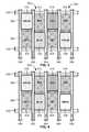
- FIG. 3shows a top view of an integrated circuit layout for a pixel 300 which is a staggered architecture for a RGB bottom emission pixel.
- the integrated circuit layout of the pixel 300includes a top subrow 302 and a bottom subrow 304 each having a series of OLEDs.
- Each of the OLEDsconstitute a sub-pixel in the individual pixels such as the pixel 300 .
- the sub-pixels(e.g. green, red and blue) alternate between the subrows.
- the top subrow 302includes a green OLED 310 , a drive transistor 312 , a red OLED 314 and a drive transistor 316 .
- the bottom subrow 304includes a drive transistor 320 , a blue OLED 322 , a drive transistor 324 and a green OLED 326 .
- a select line 330is fabricated on top of the top subrow 302 and a select line 332 is fabricated on the bottom of the bottom subrow 304 .
- the drive transistor 316 and the green OLED 326belong to a next pixel 350 in the array and share the select lines 330 and 332 with the pixel 300 .
- the OLEDs 310 , 314 and 322 in the pixel 300are therefore in staggered arrangement allowing them to be placed closer together side by side. It is to be understood that the term subrow is simply used for convenience. From another perspective, the different OLEDs may be staggered on adjacent columns.
- the various OLEDsare arranged so certain OLEDs are next to each other and other OLEDs are above or below the OLEDs next to each other in order to allow the increase in the width of the OLEDs.
- a power line 340borders both the green OLED 310 and the drive transistor 320 .
- a data line 342is fabricated between the green OLED 310 and the drive transistor 312 of the top subrow 302 and continues between the drive transistor 320 and the blue OLED 322 of the bottom subrow 304 .
- a power line 344is fabricated between the drive transistor 312 and the red OLED 314 of the top subrow 302 and continues between the blue OLED 322 and the drive transistor 324 of the bottom subrow 304 .
- the structure of the pixel 300also includes a data line 346 fabricated between the red OLED 314 and the drive transistor 314 of the top subrow 302 and continues between the transistor 324 and the green OLED 326 of the bottom subrow 304 .
- Another power line 348borders the drive transistor 316 of the top subrow 302 and the green OLED 326 of the bottom subrow 304 .
- the drive transistor 316 and the green OLED 326are part of the next pixel 350 adjacent to the pixel 300 but share the data line 346 .
- the display circuit of the pixel 300is divided into the two subrows 302 and 304 .
- the OLEDs 310 , 322 and 314are put on top and bottom side of the pixel area alternatively.
- the distance between two adjacent OLEDswill be larger than the minimum required distance.
- the data lines such as the data lines 342 and 346may be shared between two adjacent pixels such as the pixel 300 and the adjacent pixel 350 .
- FIG. 4shows an example staggered architecture for a RGBW bottom emission display pixel circuit 400 .
- the integrated circuit layout for the pixel 400includes a top subrow 402 and a bottom subrow 404 .
- the top subrow 402includes a green OLED 410 , a drive transistor 412 , a red OLED 414 and a drive transistor 416 .
- the bottom subrow 404includes a drive transistor 420 , a blue OLED 422 , a drive transistor 424 and a white OLED 426 .
- FIG. 4shows the entire pixel which includes the four OLEDs 410 , 414 , 422 and 426 .
- a select line 430is fabricated on top of the top subrow 402 and a select line 432 is fabricated on the bottom of the bottom subrow 404 .
- a power line 440borders both the green OLED 410 and the drive transistor 420 .
- a data line 442is fabricated between the green OLED 410 and the drive transistor 412 of the top subrow 402 and continues between the drive transistor 420 and the blue OLED 422 of the bottom subrow 404 .
- a power line 444is fabricated between the drive transistor 412 and the red OLED 414 of the top subrow 402 and continues between the blue OLED 422 and the drive transistor 424 of the bottom subrow 404 .
- the circuit 400also includes a data line 446 fabricated between the red OLED 414 and the drive transistor 416 of the top subrow 402 and continues between the drive transistor 424 and the white OLED 426 of the bottom subrow 404 .
- Another power line 448borders the drive transistor 416 of the top subrow 402 and the white OLED 426 of the bottom subrow 404 .
- the power lines 440 and 448are shared by adjacent pixels (not shown).
- the pixel circuit 400 in FIG. 4has increased aperture because the distance between parallel OLEDs may be decreased due to the staggered relationship between the OLEDs 410 , 414 , 422 and 426 .
- the white OLED 426is added since most of the display using the pixel circuit 400 typically emits white color and the white OLED 426 reduces continuous emissions from the blue OLED 422 which is primarily employed to emit white color in RGB type pixels such as the pixel 300 in FIG. 3 .
- the distances between the OLEDsmay be decreased resulting in greater exposure of the emission surface areas. Further, the sharing of the data and power supply lines also reduces the area necessary for such lines resulting in additional surface emission area being exposed for the OLEDs.
- FIG. 5shows a staggered color patterning for a RGB top-emission display structure 500 .
- the structure 500includes a top subrow 502 and a bottom subrow 504 .
- the top subrow 502includes a green OLED 512 and a red OLED 514 .
- the drive transistors to drive the OLEDs 512 and 514are mounted on a lower circuit layer 516 under the OLEDs 512 and 514 .
- the bottom subrow 504includes a blue OLED 522 and a green OLED 524 .
- Drive transistors that drive the OLEDs 522 and 524are fabricated on a circuit layer 526 under the OLEDs 522 and 524 .
- the OLEDs 512 , 514 and 522make up one pixel, while the green OLED 524 is part of another pixel.
- the structure 500results in a display with interlocked pixels which share various data lines. Such pixels require some interpolation of image data since the data lines are shared between the OLEDs of the pixels.
- a select line 530is fabricated on top of the top subrow 502 and a select line 532 is fabricated on the bottom of the bottom subrow 504 .
- a power line 540borders both the green OLED 510 and the blue OLED 520 .
- a data line 542is fabricated under the green OLED 510 and of the top subrow 502 and continues under the blue OLED 522 of the bottom subrow 504 .
- the data line 542is used to program the green OLED 512 and the blue OLED 522 .
- a power line 544is fabricated between the green OLED 512 and the red OLED 514 of the top subrow 502 and continues between the blue OLED 522 and the green OLED 524 of the bottom subrow 504 .
- the data line 546is used to program the red OLED 514 and the green OLED 524 .
- Another power line 548borders the red OLED 514 of the top subrow 502 and the green OLED 524 of the bottom subrow 504 .
- the power lines 540 and 548are shared by the transistors and OLEDs of adjacent pixels.
- VDATAdata programming lines 542 and 546
- the emission structure 500allows reduction of distance between the OLEDs 512 and 522 because of the staggered arrangement.
- the OLEDs 512 , 514 , 522 and 524may be made wider than a known OLED, but with a relatively shorter length. The wider OLED surface results in increased aperture ratio.
- the emission structure 500requires a processed image data signal from a raw RGB signal because the OLEDs are staggered with OLEDs from the adjacent pixels.
- the transparent common electrode (not shown) over the OLEDs 512 , 514 , 522 and 524has relatively lower resistance because of the wider areas of the OLEDs 512 , 514 , 522 and 524 .
- FIG. 6shows an alternate pixel arrangement 600 for a top emission structure.
- the pixel arrangement 600improves the aperture ratio and relaxes OLED manufacturing requirements.
- the pixel arrangement 600includes different pixels 602 , 604 , 606 and 608 .
- Each of the pixelshas three OLEDs such as OLEDs 610 , 612 and 614 which are disposed on a circuit layer 616 that includes the drive transistors to drive each of the OLEDs 610 , 612 and 614 .
- the OLED 610emits green light and is in a row with the OLED 612 that emits red light.
- the OLED 614emits a blue light and has a larger emission surface than the OLEDs 610 and 612 .
- Select linessuch as select lines 620 , 622 and 624 run on the top and the bottom of the pixels 602 , 604 , 606 and 608 .
- Power supply lines 630 , 632 and 634run along the sides of the pixels 602 , 604 , 606 and 608 to supply voltages for the OLEDs 610 , 612 and 614 and their respective drive transistors.
- Data lines 640 , 642 , 644 and 646run under the OLEDs of the pixels 602 , 604 , 606 and 608 .
- the data line 640is used to program the OLED 610
- the data line 642is used to program the OLED 612
- either data line 640 or 644is used to program the OLED 614 in the pixel 602 .
- any single currentis within one sub-row.
- the lineslook straighter in a display composed of pixels using the arrangement 600 and so provide better quality for text application.
- the OLED 614 that emits blue lightis larger than the OLEDs 610 and 612 , covering substantially the entire width of the pixel 602 , because the increased surface area for the blue color OLED 614 retards aging which is the result of inherent faster aging for a blue color OLED.
- the increased surface arearequires lower current density to produce the same output as a smaller surface OLED and therefore ages slower.
- the structure 600 in FIG. 6has an improved appearance over the structure 500 in FIG. 5 because the red, green and blue OLED elements are in a straight line as opposed to being staggered between pixels.
- the transparent common electrode (not shown) over the OLEDs 610 , 612 and 614has relatively lower resistance because of the wider areas of the OLEDs 610 , 612 and 614 , as shown in FIG. 9E .
- FIG. 7shows the cross section of a pixel structure 700 that is a modified bottom emission type pixel that increases aperture ratio by having a reflector focus light emitted from the areas of the emission area of an OLED 702 that are covered by other circuit components.
- the OLED 702includes a cathode layer 704 and an anode layer 706 .
- a common electrode layer 708provides electrical bias to the other side of the OLED 702 .
- the common electrode 708can be shaped as a concave mirror to reflect more light toward the reflective surface 740 .
- a drive transistor 710is fabricated over part of the emission surface of the OLED 702 .
- the drive transistor 710includes a gate 712 , a drain region 714 and a source region 716 .
- the drive transistor 710is fabricated on a clear substrate layer 720 that overlays the OLED 702 .
- a metallization layer 730is overlaid on the clear substrate 720 to form electrodes 732 and 734 contacting the drain region 714 and the source region 716 of the drive transistor 710 respectively and provide electrical connections to the other components of the circuit such as data and voltage supply lines.
- An electrode(not shown) is also formed to the gate of the transistor 710 .
- the metallization layer 730includes an aperture 736 through which light from the OLED 702 may be emitted through the clear substrate 720 .
- the pixel structureincludes a reflector 740 that is disposed between the OLED 702 and the drive transistor 710 .
- the reflector 740includes a reflective surface 742 facing the emission surface of the OLED 702 that reflects light emitted from the OLED 702 that would be normally blocked by the drive transistor 710 .
- the reflected light(shown in arrows in FIG. 7 ) is emitted out a window 744 in the reflector 740 to therefore increase the light actually emitted from the OLED 702 .
- the OLED emission areais not limited to the opening window which is defined by the drive transistor and supporting components on the OLED 702 .
- the OLED current density for a given luminanceis lower than a conventional bottom emission arrangement.
- This arrangement including the reflector 740requires lower OLED voltage and therefore lower power consumption to achieve the same luminance as a conventional OLED without the reflector.
- the lifetime of the OLED 702will be longer due to lower current density.
- This structure 700may also be used with other techniques to further improve aperture ratio.
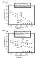
- the aperture ratio for different display resolutionsis demonstrated in a graph 800 in FIG. 8A .
- the graph 800compares the aperture ratios of various configurations to display resolutions.
- One set of data points 802shows the aperture ratios of a standard amorphous silicon red green blue pixel stripe structure as shown in FIG. 1A .
- a second set of data points 804shows the aperture ratios of a standard polysilicon red green blue pixel stripe structure. As shown in FIG. 8A , the polysilicon based pixel has slightly better aperture ratios than the amorphous silicon based pixel.
- a third set of data points 806shows the aperture ratios of a bottom emission staggered structure such as the structure of the pixel 300 shown in FIG. 3 . As shown in the data points 802 in FIG.
- the aperture ratio of the staggered pixel architecture in FIG. 3 in data points 806is higher than 20% for up to 260 PPI.
- FIG. 8Bis a graph 850 showing the plots of aperture ratios at different display resolutions for various OLED pixel structures.
- One set of data points 852shows the aperture ratios of a standard amorphous silicon red green blue pixel stripe structure as shown in FIG. 1A fabricated with a shadow mask.
- a second set of data points 854shows the aperture ratios of an amorphous silicon bottom emission staggered structure such as the structure of the pixel 300 shown in FIG. 3 fabricated with a shadow mask.
- Another set of data points 856shows the aperture ratios of a top emission type structure in a red green blue pixel strip structure fabricated by laser induced thermal imaging (LITI).
- a final set of data points 858shows the aperture ratios of a top emission type structure using the staggered arrangement shown in FIG. 7 fabricated by LITI.
- LITIlaser induced thermal imaging
- the aperture ratiois extracted for two types of OLED patterning (shadow mask with a 20- ⁇ m gap and LITI with a 10- ⁇ m gap) as shown in the data points 852 and 856 for a stripe type arrangement as shown in FIG. 1A .
- the aperture ratio for RGB stripeis limited by OLED design rules whereas a RGB stripe using LITI fabrication is limited by the TFT design rules.
- staggered color patterningcan provide high resolution (e.g. 300 ppi) with large aperture ratio as shown by the data points 854 and 858 . This resolution is provided without mandating tighter design rules as compared with conventional OLED layouts.
- a preferred method of fabricating the pixel structure described aboveby (1) forming a first photoresist layer with the first opening 736 on the substrate 720 , forming the reflective layer 740 with the second opening 744 over the first photoresist layer, forming a second photoresist layer in the opening 744 and over the reflective layer; and forming the organic light emitting device 702 over the second photoresist layer.
- the second opening 744overlaps the first opening 736 , and at least a portion of the reflective layer 740 is concave in shape.
- the transistor elements 710 , 712 , 714 , 716 , 732 and 734are formed on the surface of the substrate 720 below the reflective layer, offset from the openings 736 and 744 .
- FIGS. 9A-9Mare cross-sectional views illustrating successive steps of one exemplary fabrication process for a pixel structure having a high effective aperture ratio according to an embodiment of the invention. These steps can be used to manufacture a pixel structure as shown.
- the pixel structureis a modified bottom emission type pixel that increases effective aperture ratio, such that the effective aperture ratio is larger than the actual aperture ratio of the device.
- the transistor circuits supporting the pixel structureare omitted.
- the pixel structure of FIGS. 9A-9Mcan include one or more supporting transistors (e.g., TFTs), such as drive transistor 710 and its associated components, positioned as shown in FIG. 7 .
- a substrate 910is provided.
- Substrate 910may be, for example, a glass wafer.
- Substrate 910is cleaned with an RCA solution; specifically, a 1:1:5 solution of NH 4 OH (ammonium hydroxide), H 2 O 2 (hydrogen peroxide), and H 2 O (water), respectively.
- Substrate 910is cleaned with the solution at 80° C. for 20 minutes.
- a first photoresist layer 915is formed to a thickness of 11.6 ⁇ m on substrate 910 , as shown in FIG. 9A .
- first photoresist layer 915is spin coated on substrate 910 at 800 rpm for 10 seconds, then at 4000 rpm for 60 seconds.
- First photoresist layer 915may comprise any suitable transparent photoresist material, such as, for example, SU-8 photoresist.
- first photoresist layer 915comprises a black or dark polymer.
- First photoresist layer 915is then soft baked at 95° C. for 3 minutes, exposed for 16 seconds, and hard baked at 95° C. for 4 minutes.
- a mask layer 920is formed to a thickness of 100 nm on first photoresist layer 915 .
- Mask layer 920is used as a hard mask for later etching of first photoresist layer 915 and can be, for example, an aluminum film.
- mask layer 920is deposited using WLOS sputtering with 50 sccm Ar, 9 mTorr pressure, 300 W DC power, and 700 seconds deposition time.
- a second photoresist layer 925is formed on mask layer 920 for photolithography, as shown in FIG. 9C .
- second photoresist layer 925is spin coated on mask layer 920 at 500 rpm for 10 seconds, then at 4000 rpm for 60 seconds.
- Second photoresist layer 925may comprise any suitable photoresist material such as, for example, AZ3312 photoresist. Second photoresist layer 925 is then soft baked at 90° C. for 1 minute.
- Photo mask 930 a - cis then applied to second photoresist layer 925 , and ultraviolent (UV) exposure is applied from the top (i.e., on the side of photo mask 930 a - c ), as shown in FIG. 9D .
- UV exposureis maintained for 4 seconds with an intensity of 10 mW/cm 2 .
- AZ 300 MIF developeris then applied and developed for 16 seconds, and the sample is post-exposure baked at 120° C. for 60 seconds, resulting in separate second photoresist layers 925 a and 925 b.
- mask layer 920is etched into separate mask layers 920 a and 920 b .
- mask layer 920is etched using a polyacrylonitrile (PAN) solution; specifically, a 16:2:1:1 solution of H 3 PO 4 (phosphoric acid), H 2 O (deionized water), HAc (acetic acid), and HNO 3 (nitric acid), respectively, is used.
- PANpolyacrylonitrile
- Mask layer 920is etched at 40° C. for 3-4 minutes.
- second photoresist layers 925 a and 925 bare removed.
- second photoresist layers 925 a and 925 bare removed using acetone or AZ300 stripper.
- First photoresist layer 915is then etched into separate first photoresist layers 915 a , 915 b , as shown in FIG. 9G , forming a concave shape.
- first photoresist layeris isotropically dry etched using inductively coupled plasma (ICP).
- ICP dry etching recipeis: 20 O 2 , 2 CF 4 , 180 ICP power, 50 pressure, and 700 seconds etching time.
- FIG. 9Hseparate mask layers 920 a and 920 b are removed.
- separate mask layers 920 a and 920 bare removed using a polyacrylonitrile (PAN) solution.
- PANpolyacrylonitrile
- Reflective layer 940is then deposited, as shown in FIG. 9I .
- reflective layer 940is deposited using WLOS sputtering with 50 sccm Ar, 9 mTorr pressure, 300 W DC power, and 700 seconds deposition time.
- the emission windowsare then opened using photopithography.
- a third photoresist layer(not shown) is spin coated at 3000 rpm for 30 seconds, soft baked at 100° C. for 6 minutes, then re-hydrated for 30 minutes.
- the third photoresist layercan comprise any suitable photoresist layer, and in this embodiment, comprises AZ P4330 photoresist.
- the third photoresist layeris then exposed to 365 nm ultraviolet radiation for 35 seconds, and developed in a 1:4 solution of AZ400K developer and deionized water, respectively, for 6 minutes.
- the portion of mirror layer 940 on substrate 910is then etched with polyacrylonitrile for 4 minutes, resulting in separate mirror layers 940 a and 940 b , and the rest of the third photoresist later is removed using stripper.
- a fourth photoresist layer 945is deposited in the opening of mirror layers 940 a and 940 b , and over reflective layers 940 a and 940 b .
- fourth photoresist layer 945is spin coated at 800 rpm for 10 seconds, then at 4000 rpm for 60 seconds.
- Fourth photoresist layer 945may comprise any suitable transparent photoresist material, such as, for example, SU-8 photoresist.
- Fourth photoresist layer 945is then soft baked at 95° C. for 3 minutes, exposed for 16 seconds, and hard baked at 95° C. for 4 minutes.
- Anode 950is then deposited over fourth photoresist layer 945 , as shown in FIG. 9L .
- anode 950is an indium tin oxide (ITO) film.
- Anode 950is deposited using an AJA sputtering system with a ratio of Ar:O 2 of 16:0.5, a temperature of 150° C., RF power of 100 W, and deposition time of 50 minutes. Post-annealing is then conducted at 150° C. for 30 minutes.
- Anode 950can then be patterned using another photolithography process.
- OLEDsare then deposited on top of the patterned anode 950 , as shown in FIG. 9M .
- the OLEDsare deposited using an InteVoc thermal evaporation system at a pressure under 5 ⁇ 10 ⁇ 6 Torr.
- the OLEDscomprise anode 950 , organic electroluminescent layer 955 , and cathode 960 .
- a common electrode layer(not shown) can be formed over cathode 960 .
- organic electroluminescent layer 955can comprise a plurality of layers, including (from anode 950 to cathode 960 ) a hole injection layer, a hole transport layer, an emission layer, an electron transport layer and an electron injection layer.
- the hole injection layercomprises MoO 3 ;
- the hole transport layercomprises NPB;
- the electron transport layercomprises Alq 3 ;
- the electron injection layercomprises LiF; and
- cathode 960comprises Al.
- the pixel structureincludes reflective layers 940 a , 940 b that are disposed between the OLED (comprising anode 950 , organic electroluminescent layer 955 , and cathode 960 ) and the drive transistor(s) (not shown, but positioned between the substrate and first photoresist layers 915 a and 915 b ).
- Reflective layers 940 a , 940 binclude a reflective surface facing the emission surface of the OLED that reflects light emitted from the OLED that would be normally blocked by the drive transistor(s). The reflected light is emitted out an opening between mirror layers 940 a and 940 b to therefore increase the light actually emitted from the OLED. Because of the concave shape of reflective layers 940 a and 940 b , reflected light (as well as ambient light) is guided toward the opening between reflective layers 940 a and 940 b.
- the OLED emission areais not limited to the opening window which is defined by the drive transistor and supporting components on the OLED.
- the OLED current density for a given luminanceis lower than a conventional bottom emission arrangement.
- This arrangement including reflective layers 940 a , 940 brequires lower OLED voltage and therefore lower power consumption to achieve the same luminance as a convention OLED without the mirror layers.
- the lifetime of the OLEDwill be longer due to lower current density.
- This structuremay also be used with other techniques to further improve effective aperture ratio.
Landscapes
- Physics & Mathematics (AREA)
- Engineering & Computer Science (AREA)
- Geometry (AREA)
- Microelectronics & Electronic Packaging (AREA)
- Optics & Photonics (AREA)
- Electroluminescent Light Sources (AREA)
- Manufacturing & Machinery (AREA)
Abstract
Description
Claims (1)
Priority Applications (1)
| Application Number | Priority Date | Filing Date | Title |
|---|---|---|---|
| US14/322,995US9059117B2 (en) | 2009-12-01 | 2014-07-03 | High resolution pixel architecture |
Applications Claiming Priority (5)
| Application Number | Priority Date | Filing Date | Title |
|---|---|---|---|
| CA2686174 | 2009-12-01 | ||
| CA2686174ACA2686174A1 (en) | 2009-12-01 | 2009-12-01 | High reslution pixel architecture |
| US12/958,035US8552636B2 (en) | 2009-12-01 | 2010-12-01 | High resolution pixel architecture |
| US13/724,424US8803417B2 (en) | 2009-12-01 | 2012-12-21 | High resolution pixel architecture |
| US14/322,995US9059117B2 (en) | 2009-12-01 | 2014-07-03 | High resolution pixel architecture |
Related Parent Applications (1)
| Application Number | Title | Priority Date | Filing Date |
|---|---|---|---|
| US13/724,424ContinuationUS8803417B2 (en) | 2009-12-01 | 2012-12-21 | High resolution pixel architecture |
Publications (2)
| Publication Number | Publication Date |
|---|---|
| US20140312333A1 US20140312333A1 (en) | 2014-10-23 |
| US9059117B2true US9059117B2 (en) | 2015-06-16 |
Family
ID=48223100
Family Applications (2)
| Application Number | Title | Priority Date | Filing Date |
|---|---|---|---|
| US13/724,424ActiveUS8803417B2 (en) | 2009-12-01 | 2012-12-21 | High resolution pixel architecture |
| US14/322,995ActiveUS9059117B2 (en) | 2009-12-01 | 2014-07-03 | High resolution pixel architecture |
Family Applications Before (1)
| Application Number | Title | Priority Date | Filing Date |
|---|---|---|---|
| US13/724,424ActiveUS8803417B2 (en) | 2009-12-01 | 2012-12-21 | High resolution pixel architecture |
Country Status (1)
| Country | Link |
|---|---|
| US (2) | US8803417B2 (en) |
Cited By (2)
| Publication number | Priority date | Publication date | Assignee | Title |
|---|---|---|---|---|
| DE102015223707A1 (en) | 2014-11-28 | 2016-06-16 | Ignis Innovation Inc. | Array architecture with high pixel density |
| US20160254326A1 (en)* | 2014-09-30 | 2016-09-01 | Boe Technology Group Co., Ltd. | Oled display substrate, oled display device, and mask |
Families Citing this family (73)
| Publication number | Priority date | Publication date | Assignee | Title |
|---|---|---|---|---|
| CA2443206A1 (en) | 2003-09-23 | 2005-03-23 | Ignis Innovation Inc. | Amoled display backplanes - pixel driver circuits, array architecture, and external compensation |
| US10013907B2 (en) | 2004-12-15 | 2018-07-03 | Ignis Innovation Inc. | Method and system for programming, calibrating and/or compensating, and driving an LED display |
| US9275579B2 (en) | 2004-12-15 | 2016-03-01 | Ignis Innovation Inc. | System and methods for extraction of threshold and mobility parameters in AMOLED displays |
| TWI402790B (en) | 2004-12-15 | 2013-07-21 | Ignis Innovation Inc | Method and system for programming, calibrating and driving a light-emitting element display |
| US9280933B2 (en) | 2004-12-15 | 2016-03-08 | Ignis Innovation Inc. | System and methods for extraction of threshold and mobility parameters in AMOLED displays |
| US8576217B2 (en) | 2011-05-20 | 2013-11-05 | Ignis Innovation Inc. | System and methods for extraction of threshold and mobility parameters in AMOLED displays |
| US9799246B2 (en) | 2011-05-20 | 2017-10-24 | Ignis Innovation Inc. | System and methods for extraction of threshold and mobility parameters in AMOLED displays |
| US10012678B2 (en) | 2004-12-15 | 2018-07-03 | Ignis Innovation Inc. | Method and system for programming, calibrating and/or compensating, and driving an LED display |
| JP5355080B2 (en) | 2005-06-08 | 2013-11-27 | イグニス・イノベイション・インコーポレーテッド | Method and system for driving a light emitting device display |
| CA2518276A1 (en) | 2005-09-13 | 2007-03-13 | Ignis Innovation Inc. | Compensation technique for luminance degradation in electro-luminance devices |
| TW200746022A (en) | 2006-04-19 | 2007-12-16 | Ignis Innovation Inc | Stable driving scheme for active matrix displays |
| CA2556961A1 (en) | 2006-08-15 | 2008-02-15 | Ignis Innovation Inc. | Oled compensation technique based on oled capacitance |
| CA2688870A1 (en) | 2009-11-30 | 2011-05-30 | Ignis Innovation Inc. | Methode and techniques for improving display uniformity |
| CA2669367A1 (en) | 2009-06-16 | 2010-12-16 | Ignis Innovation Inc | Compensation technique for color shift in displays |
| US9311859B2 (en) | 2009-11-30 | 2016-04-12 | Ignis Innovation Inc. | Resetting cycle for aging compensation in AMOLED displays |
| US9384698B2 (en) | 2009-11-30 | 2016-07-05 | Ignis Innovation Inc. | System and methods for aging compensation in AMOLED displays |
| US10319307B2 (en) | 2009-06-16 | 2019-06-11 | Ignis Innovation Inc. | Display system with compensation techniques and/or shared level resources |
| US10996258B2 (en) | 2009-11-30 | 2021-05-04 | Ignis Innovation Inc. | Defect detection and correction of pixel circuits for AMOLED displays |
| US8803417B2 (en) | 2009-12-01 | 2014-08-12 | Ignis Innovation Inc. | High resolution pixel architecture |
| US10163401B2 (en) | 2010-02-04 | 2018-12-25 | Ignis Innovation Inc. | System and methods for extracting correlation curves for an organic light emitting device |
| US20140313111A1 (en) | 2010-02-04 | 2014-10-23 | Ignis Innovation Inc. | System and methods for extracting correlation curves for an organic light emitting device |
| CA2692097A1 (en) | 2010-02-04 | 2011-08-04 | Ignis Innovation Inc. | Extracting correlation curves for light emitting device |
| US9881532B2 (en) | 2010-02-04 | 2018-01-30 | Ignis Innovation Inc. | System and method for extracting correlation curves for an organic light emitting device |
| US10176736B2 (en) | 2010-02-04 | 2019-01-08 | Ignis Innovation Inc. | System and methods for extracting correlation curves for an organic light emitting device |
| US10089921B2 (en) | 2010-02-04 | 2018-10-02 | Ignis Innovation Inc. | System and methods for extracting correlation curves for an organic light emitting device |
| CA2696778A1 (en) | 2010-03-17 | 2011-09-17 | Ignis Innovation Inc. | Lifetime, uniformity, parameter extraction methods |
| US8907991B2 (en) | 2010-12-02 | 2014-12-09 | Ignis Innovation Inc. | System and methods for thermal compensation in AMOLED displays |
| US9530349B2 (en) | 2011-05-20 | 2016-12-27 | Ignis Innovations Inc. | Charged-based compensation and parameter extraction in AMOLED displays |
| US9466240B2 (en) | 2011-05-26 | 2016-10-11 | Ignis Innovation Inc. | Adaptive feedback system for compensating for aging pixel areas with enhanced estimation speed |
| US9773439B2 (en) | 2011-05-27 | 2017-09-26 | Ignis Innovation Inc. | Systems and methods for aging compensation in AMOLED displays |
| US9324268B2 (en) | 2013-03-15 | 2016-04-26 | Ignis Innovation Inc. | Amoled displays with multiple readout circuits |
| US10089924B2 (en) | 2011-11-29 | 2018-10-02 | Ignis Innovation Inc. | Structural and low-frequency non-uniformity compensation |
| US8937632B2 (en) | 2012-02-03 | 2015-01-20 | Ignis Innovation Inc. | Driving system for active-matrix displays |
| US9747834B2 (en) | 2012-05-11 | 2017-08-29 | Ignis Innovation Inc. | Pixel circuits including feedback capacitors and reset capacitors, and display systems therefore |
| US8922544B2 (en) | 2012-05-23 | 2014-12-30 | Ignis Innovation Inc. | Display systems with compensation for line propagation delay |
| US9786223B2 (en) | 2012-12-11 | 2017-10-10 | Ignis Innovation Inc. | Pixel circuits for AMOLED displays |
| US9336717B2 (en) | 2012-12-11 | 2016-05-10 | Ignis Innovation Inc. | Pixel circuits for AMOLED displays |
| US20140166991A1 (en)* | 2012-12-17 | 2014-06-19 | Dmitri E. Nikonov | Transparent light-emitting display |
| CN104871337A (en)* | 2012-12-21 | 2015-08-26 | 伊格尼斯创新公司 | High resolution pixel architecture |
| CN108665836B (en) | 2013-01-14 | 2021-09-03 | 伊格尼斯创新公司 | Method and system for compensating for deviations of a measured device current from a reference current |
| US9830857B2 (en) | 2013-01-14 | 2017-11-28 | Ignis Innovation Inc. | Cleaning common unwanted signals from pixel measurements in emissive displays |
| EP3043338A1 (en) | 2013-03-14 | 2016-07-13 | Ignis Innovation Inc. | Re-interpolation with edge detection for extracting an aging pattern for amoled displays |
| WO2014174427A1 (en) | 2013-04-22 | 2014-10-30 | Ignis Innovation Inc. | Inspection system for oled display panels |
| CN105474296B (en) | 2013-08-12 | 2017-08-18 | 伊格尼斯创新公司 | A method and device for driving a display using image data |
| US9761170B2 (en) | 2013-12-06 | 2017-09-12 | Ignis Innovation Inc. | Correction for localized phenomena in an image array |
| US9741282B2 (en) | 2013-12-06 | 2017-08-22 | Ignis Innovation Inc. | OLED display system and method |
| US9502653B2 (en) | 2013-12-25 | 2016-11-22 | Ignis Innovation Inc. | Electrode contacts |
| CN103778888B (en)* | 2014-01-27 | 2016-02-17 | 北京京东方光电科技有限公司 | Display panel and driving method thereof |
| DE102015206281A1 (en) | 2014-04-08 | 2015-10-08 | Ignis Innovation Inc. | Display system with shared level resources for portable devices |
| CN103996693B (en)* | 2014-04-24 | 2016-05-11 | 京东方科技集团股份有限公司 | Oled panel and preparation method thereof, display unit |
| CA2879462A1 (en) | 2015-01-23 | 2016-07-23 | Ignis Innovation Inc. | Compensation for color variation in emissive devices |
| CN104716163B (en) | 2015-03-26 | 2018-03-16 | 京东方科技集团股份有限公司 | Dot structure and display base plate and display device |
| CN104716167B (en) | 2015-04-13 | 2017-07-25 | 京东方科技集团股份有限公司 | An organic electroluminescence display device, its manufacturing method and display device |
| CA2889870A1 (en) | 2015-05-04 | 2016-11-04 | Ignis Innovation Inc. | Optical feedback system |
| CA2892714A1 (en) | 2015-05-27 | 2016-11-27 | Ignis Innovation Inc | Memory bandwidth reduction in compensation system |
| CA2900170A1 (en) | 2015-08-07 | 2017-02-07 | Gholamreza Chaji | Calibration of pixel based on improved reference values |
| KR102475504B1 (en)* | 2015-08-20 | 2022-12-09 | 엘지디스플레이 주식회사 | Transparent display pannel transparent display device including the same |
| JP6535545B2 (en) | 2015-08-21 | 2019-06-26 | 株式会社ジャパンディスプレイ | Display device |
| US10431634B2 (en)* | 2015-09-10 | 2019-10-01 | Sharp Kabushiki Kaisha | Organic electroluminescence device with recesses filled with a phosphor filling layer in the base material |
| KR102440237B1 (en)* | 2015-11-03 | 2022-09-05 | 엘지디스플레이 주식회사 | Organic light emitting diode display device |
| CN109565917B (en)* | 2016-07-28 | 2021-01-15 | 夏普株式会社 | Method for manufacturing display device and display device |
| CN106229300B (en)* | 2016-08-23 | 2019-03-22 | 武汉华星光电技术有限公司 | Dot structure and production method |
| KR102714947B1 (en) | 2016-08-31 | 2024-10-07 | 엘지디스플레이 주식회사 | Organic light emitting display device |
| CN107565040A (en)* | 2017-08-30 | 2018-01-09 | 深圳市华星光电半导体显示技术有限公司 | Oled substrate and preparation method thereof |
| KR102650950B1 (en) | 2017-09-29 | 2024-03-26 | 서울반도체 주식회사 | Light emitting device for display and display apparatus having the same |
| CN109817664B (en) | 2017-11-22 | 2021-01-22 | 京东方科技集团股份有限公司 | Display substrate and preparation method thereof, and display panel |
| US11244930B2 (en)* | 2018-08-10 | 2022-02-08 | Innolux Corporation | Electronic device with light emitting units with reduced power consumption |
| CN109119028B (en)* | 2018-09-07 | 2020-04-28 | 武汉华星光电半导体显示技术有限公司 | AMOLED display panel and corresponding display device |
| CN109377942B (en)* | 2018-12-24 | 2020-07-03 | 合肥鑫晟光电科技有限公司 | Compensation method, device and display device for display device |
| TWI686791B (en)* | 2019-02-26 | 2020-03-01 | 友達光電股份有限公司 | Light emitting diode display apparatus |
| KR102821554B1 (en)* | 2019-09-30 | 2025-06-16 | 엘지디스플레이 주식회사 | Display device |
| CN110718575B (en)* | 2019-10-22 | 2022-08-23 | 京东方科技集团股份有限公司 | Transparent OLED display panel, display device and driving method |
| WO2021108903A1 (en)* | 2019-12-02 | 2021-06-10 | Vuereal Inc. | Creating staging in backplane for micro device integration |
Citations (486)
| Publication number | Priority date | Publication date | Assignee | Title |
|---|---|---|---|---|
| US3506851A (en) | 1966-12-14 | 1970-04-14 | North American Rockwell | Field effect transistor driver using capacitor feedback |
| US3774055A (en) | 1972-01-24 | 1973-11-20 | Nat Semiconductor Corp | Clocked bootstrap inverter circuit |
| US4090096A (en) | 1976-03-31 | 1978-05-16 | Nippon Electric Co., Ltd. | Timing signal generator circuit |
| US4160934A (en) | 1977-08-11 | 1979-07-10 | Bell Telephone Laboratories, Incorporated | Current control circuit for light emitting diode |
| US4354162A (en) | 1981-02-09 | 1982-10-12 | National Semiconductor Corporation | Wide dynamic range control amplifier with offset correction |
| EP0158366B1 (en) | 1984-04-13 | 1990-01-24 | Sharp Kabushiki Kaisha | Color liquid-crystal display apparatus |
| US4943956A (en) | 1988-04-25 | 1990-07-24 | Yamaha Corporation | Driving apparatus |
| US4996523A (en) | 1988-10-20 | 1991-02-26 | Eastman Kodak Company | Electroluminescent storage display with improved intensity driver circuits |
| CA1294034C (en) | 1985-01-09 | 1992-01-07 | Hiromu Hosokawa | Color uniformity compensation apparatus for cathode ray tubes |
| JPH04158570A (en) | 1990-10-22 | 1992-06-01 | Seiko Epson Corp | Structure of semiconductor device and manufacture thereof |
| US5153420A (en) | 1990-11-28 | 1992-10-06 | Xerox Corporation | Timing independent pixel-scale light sensing apparatus |
| JPH0442619Y2 (en) | 1987-07-10 | 1992-10-08 | ||
| CA2109951A1 (en) | 1991-05-24 | 1992-11-26 | Robert Hotto | Dc integrating display driver employing pixel status memories |
| US5198803A (en) | 1990-06-06 | 1993-03-30 | Opto Tech Corporation | Large scale movie display system with multiple gray levels |
| US5204661A (en) | 1990-12-13 | 1993-04-20 | Xerox Corporation | Input/output pixel circuit and array of such circuits |
| US5266515A (en) | 1992-03-02 | 1993-11-30 | Motorola, Inc. | Fabricating dual gate thin film transistors |
| JPH06314977A (en) | 1993-04-28 | 1994-11-08 | Nec Ic Microcomput Syst Ltd | Current output type d/a converter circuit |
| US5489918A (en) | 1991-06-14 | 1996-02-06 | Rockwell International Corporation | Method and apparatus for dynamically and adjustably generating active matrix liquid crystal display gray level voltages |
| US5498880A (en) | 1995-01-12 | 1996-03-12 | E. I. Du Pont De Nemours And Company | Image capture panel using a solid state device |
| US5557342A (en) | 1993-07-06 | 1996-09-17 | Hitachi, Ltd. | Video display apparatus for displaying a plurality of video signals having different scanning frequencies and a multi-screen display system using the video display apparatus |
| US5572444A (en) | 1992-08-19 | 1996-11-05 | Mtl Systems, Inc. | Method and apparatus for automatic performance evaluation of electronic display devices |
| JPH08340243A (en) | 1995-06-14 | 1996-12-24 | Canon Inc | Bias circuit |
| US5589847A (en) | 1991-09-23 | 1996-12-31 | Xerox Corporation | Switched capacitor analog circuits using polysilicon thin film technology |
| JPH0990405A (en) | 1995-09-21 | 1997-04-04 | Sharp Corp | Thin film transistor |
| US5619033A (en) | 1995-06-07 | 1997-04-08 | Xerox Corporation | Layered solid state photodiode sensor array |
| US5648276A (en) | 1993-05-27 | 1997-07-15 | Sony Corporation | Method and apparatus for fabricating a thin film semiconductor device |
| US5670973A (en) | 1993-04-05 | 1997-09-23 | Cirrus Logic, Inc. | Method and apparatus for compensating crosstalk in liquid crystal displays |
| US5691783A (en) | 1993-06-30 | 1997-11-25 | Sharp Kabushiki Kaisha | Liquid crystal display device and method for driving the same |
| US5714968A (en) | 1994-08-09 | 1998-02-03 | Nec Corporation | Current-dependent light-emitting element drive circuit for use in active matrix display device |
| US5723950A (en) | 1996-06-10 | 1998-03-03 | Motorola | Pre-charge driver for light emitting devices and method |
| US5744824A (en) | 1994-06-15 | 1998-04-28 | Sharp Kabushiki Kaisha | Semiconductor device method for producing the same and liquid crystal display including the same |
| US5745660A (en) | 1995-04-26 | 1998-04-28 | Polaroid Corporation | Image rendering system and method for generating stochastic threshold arrays for use therewith |
| US5748160A (en) | 1995-08-21 | 1998-05-05 | Mororola, Inc. | Active driven LED matrices |
| JPH10254410A (en) | 1997-03-12 | 1998-09-25 | Pioneer Electron Corp | Organic electroluminescent display device, and driving method therefor |
| US5815303A (en) | 1997-06-26 | 1998-09-29 | Xerox Corporation | Fault tolerant projective display having redundant light modulators |
| TW342486B (en) | 1994-07-18 | 1998-10-11 | Toshiba Co Ltd | LED dot matrix display device and method for dimming thereof |
| WO1998048403A1 (en) | 1997-04-23 | 1998-10-29 | Sarnoff Corporation | Active matrix light emitting diode pixel structure and method |
| US5870071A (en) | 1995-09-07 | 1999-02-09 | Frontec Incorporated | LCD gate line drive circuit |
| US5874803A (en) | 1997-09-09 | 1999-02-23 | The Trustees Of Princeton University | Light emitting device with stack of OLEDS and phosphor downconverter |
| US5880582A (en) | 1996-09-04 | 1999-03-09 | Sumitomo Electric Industries, Ltd. | Current mirror circuit and reference voltage generating and light emitting element driving circuits using the same |
| US5903248A (en) | 1997-04-11 | 1999-05-11 | Spatialight, Inc. | Active matrix display having pixel driving circuits with integrated charge pumps |
| US5917280A (en) | 1997-02-03 | 1999-06-29 | The Trustees Of Princeton University | Stacked organic light emitting devices |
| US5923794A (en) | 1996-02-06 | 1999-07-13 | Polaroid Corporation | Current-mediated active-pixel image sensing device with current reset |
| JPH11202295A (en) | 1998-01-09 | 1999-07-30 | Seiko Epson Corp | Driving circuit for electro-optical device, electro-optical device, and electronic apparatus |
| JPH11219146A (en) | 1997-09-29 | 1999-08-10 | Mitsubishi Chemical Corp | Active matrix light emitting diode pixel structure and method |
| JPH11231805A (en) | 1998-02-10 | 1999-08-27 | Sanyo Electric Co Ltd | Display device |
| US5945972A (en) | 1995-11-30 | 1999-08-31 | Kabushiki Kaisha Toshiba | Display device |
| US5949398A (en) | 1996-04-12 | 1999-09-07 | Thomson Multimedia S.A. | Select line driver for a display matrix with toggling backplane |
| US5952991A (en) | 1996-11-14 | 1999-09-14 | Kabushiki Kaisha Toshiba | Liquid crystal display |
| US5952789A (en) | 1997-04-14 | 1999-09-14 | Sarnoff Corporation | Active matrix organic light emitting diode (amoled) display pixel structure and data load/illuminate circuit therefor |
| WO1999048079A1 (en) | 1998-03-19 | 1999-09-23 | Holloman Charles J | Analog driver for led or similar display element |
| JPH11282419A (en) | 1998-03-31 | 1999-10-15 | Nec Corp | Element driving device and method and image display device |
| US5982104A (en) | 1995-12-26 | 1999-11-09 | Pioneer Electronic Corporation | Driver for capacitive light-emitting device with degradation compensated brightness control |
| US5990629A (en) | 1997-01-28 | 1999-11-23 | Casio Computer Co., Ltd. | Electroluminescent display device and a driving method thereof |
| US6023259A (en) | 1997-07-11 | 2000-02-08 | Fed Corporation | OLED active matrix using a single transistor current mode pixel design |
| JP2000056847A (en) | 1998-08-14 | 2000-02-25 | Nec Corp | Constant current driving circuit |
| JP2000081607A (en) | 1998-09-04 | 2000-03-21 | Denso Corp | Matrix type liquid crystal display device |
| CA2242720C (en) | 1998-07-09 | 2000-05-16 | Ibm Canada Limited-Ibm Canada Limitee | Programmable led driver |
| US6069365A (en) | 1997-11-25 | 2000-05-30 | Alan Y. Chow | Optical processor based imaging system |
| CA2354018A1 (en) | 1998-12-14 | 2000-06-22 | Alan Richard | Portable microdisplay system |
| US6177915B1 (en) | 1990-06-11 | 2001-01-23 | International Business Machines Corporation | Display system having section brightness control and method of operating system |
| WO2001006484A1 (en) | 1999-07-14 | 2001-01-25 | Sony Corporation | Current drive circuit and display comprising the same, pixel circuit, and drive method |
| WO2001027910A1 (en) | 1999-10-12 | 2001-04-19 | Koninklijke Philips Electronics N.V. | Led display device |
| US6229506B1 (en) | 1997-04-23 | 2001-05-08 | Sarnoff Corporation | Active matrix light emitting diode pixel structure and concomitant method |
| JP2001134217A (en) | 1999-11-09 | 2001-05-18 | Tdk Corp | Driving device for organic el element |
| US20010002703A1 (en) | 1999-11-30 | 2001-06-07 | Jun Koyama | Electric device |
| US6246180B1 (en) | 1999-01-29 | 2001-06-12 | Nec Corporation | Organic el display device having an improved image quality |
| US6252248B1 (en) | 1998-06-08 | 2001-06-26 | Sanyo Electric Co., Ltd. | Thin film transistor and display |
| US6259424B1 (en) | 1998-03-04 | 2001-07-10 | Victor Company Of Japan, Ltd. | Display matrix substrate, production method of the same and display matrix circuit |
| US6262589B1 (en) | 1998-05-25 | 2001-07-17 | Asia Electronics, Inc. | TFT array inspection method and device |
| JP2001195014A (en) | 2000-01-14 | 2001-07-19 | Tdk Corp | Driving device for organic el element |
| US20010009283A1 (en) | 2000-01-26 | 2001-07-26 | Tatsuya Arao | Semiconductor device and method of manufacturing the semiconductor device |
| US6271825B1 (en) | 1996-04-23 | 2001-08-07 | Rainbow Displays, Inc. | Correction methods for brightness in electronic display |
| WO2001063587A2 (en) | 2000-02-22 | 2001-08-30 | Sarnoff Corporation | A method and apparatus for calibrating display devices and automatically compensating for loss in their efficiency over time |
| US20010024181A1 (en) | 2000-01-17 | 2001-09-27 | Ibm | Liquid-crystal display, liquid-crystal control circuit, flicker inhibition method, and liquid-crystal driving method |
| US20010026257A1 (en) | 2000-03-27 | 2001-10-04 | Hajime Kimura | Electro-optical device |
| US6304039B1 (en) | 2000-08-08 | 2001-10-16 | E-Lite Technologies, Inc. | Power supply for illuminating an electro-luminescent panel |
| US20010030323A1 (en) | 2000-03-29 | 2001-10-18 | Sony Corporation | Thin film semiconductor apparatus and method for driving the same |
| US6307322B1 (en) | 1999-12-28 | 2001-10-23 | Sarnoff Corporation | Thin-film transistor circuitry with reduced sensitivity to variance in transistor threshold voltage |
| US6310962B1 (en) | 1997-08-20 | 2001-10-30 | Samsung Electronics Co., Ltd. | MPEG2 moving picture encoding/decoding system |
| US20010035863A1 (en) | 2000-04-26 | 2001-11-01 | Hajime Kimura | Electronic device and driving method thereof |
| US20010040541A1 (en) | 1997-09-08 | 2001-11-15 | Kiyoshi Yoneda | Semiconductor device having laser-annealed semiconductor device, display device and liquid crystal display device |
| US6320325B1 (en) | 2000-11-06 | 2001-11-20 | Eastman Kodak Company | Emissive display with luminance feedback from a representative pixel |
| US20010043173A1 (en) | 1997-09-04 | 2001-11-22 | Ronald Roy Troutman | Field sequential gray in active matrix led display using complementary transistor pixel circuits |
| US6323631B1 (en) | 2001-01-18 | 2001-11-27 | Sunplus Technology Co., Ltd. | Constant current driver with auto-clamped pre-charge function |
| US20010045929A1 (en) | 2000-01-21 | 2001-11-29 | Prache Olivier F. | Gray scale pixel driver for electronic display and method of operation therefor |
| US20010052940A1 (en) | 2000-02-01 | 2001-12-20 | Yoshio Hagihara | Solid-state image-sensing device |
| US20010052606A1 (en) | 2000-05-22 | 2001-12-20 | Koninklijke Philips Electronics N.V. | Display device |
| US20020000576A1 (en) | 2000-06-22 | 2002-01-03 | Kazutaka Inukai | Display device |
| EP1111577A3 (en) | 1999-12-24 | 2002-01-16 | Sanyo Electric Co., Ltd. | Improvements in power consumption of display apparatus during still image display mode |
| US20020011796A1 (en) | 2000-05-08 | 2002-01-31 | Semiconductor Energy Laboratory Co., Ltd. | Light-emitting device, and electric device using the same |
| US20020012057A1 (en) | 2000-05-26 | 2002-01-31 | Hajime Kimura | MOS sensor and drive method thereof |
| US20020011799A1 (en) | 2000-04-06 | 2002-01-31 | Semiconductor Energy Laboratory Co., Ltd. | Electronic device and driving method |
| US20020014851A1 (en) | 2000-06-05 | 2002-02-07 | Ya-Hsiang Tai | Apparatus and method of testing an organic light emitting diode array |
| US20020018034A1 (en) | 2000-07-31 | 2002-02-14 | Shigeru Ohki | Display color temperature corrected lighting apparatus and flat plane display apparatus |
| JP2002055654A (en) | 2000-08-10 | 2002-02-20 | Nec Corp | Electroluminescence display |
| US6356029B1 (en) | 1999-10-02 | 2002-03-12 | U.S. Philips Corporation | Active matrix electroluminescent display device |
| US20020030190A1 (en) | 1998-12-03 | 2002-03-14 | Hisashi Ohtani | Electro-optical device and semiconductor circuit |
| JP2002091376A (en) | 2000-06-27 | 2002-03-27 | Hitachi Ltd | Image display device and driving method thereof |
| US6373454B1 (en) | 1998-06-12 | 2002-04-16 | U.S. Philips Corporation | Active matrix electroluminescent display devices |
| US20020047565A1 (en) | 2000-07-28 | 2002-04-25 | Wintest Corporation | Apparatus and method for evaluating organic EL display |
| US20020052086A1 (en) | 2000-10-31 | 2002-05-02 | Mitsubishi Denki Kabushiki Kaisha | Semiconductor device and method of manufacturing same |
| US6392617B1 (en) | 1999-10-27 | 2002-05-21 | Agilent Technologies, Inc. | Active matrix light emitting diode display |
| US20020084463A1 (en) | 2001-01-04 | 2002-07-04 | International Business Machines Corporation | Low-power organic light emitting diode pixel circuit |
| US6417825B1 (en) | 1998-09-29 | 2002-07-09 | Sarnoff Corporation | Analog active matrix emissive display |
| US20020101172A1 (en) | 2001-01-02 | 2002-08-01 | Bu Lin-Kai | Oled active driving system with current feedback |
| US20020101152A1 (en) | 2001-01-30 | 2002-08-01 | Semiconductor Energy Laboratory Co., Ltd. | Light emitting device |
| US20020105279A1 (en) | 2001-02-08 | 2002-08-08 | Hajime Kimura | Light emitting device and electronic equipment using the same |
| CA2436451A1 (en) | 2001-02-05 | 2002-08-15 | International Business Machines Corporation | Liquid crystal display device |
| US6437106B1 (en) | 1999-06-24 | 2002-08-20 | Abbott Laboratories | Process for preparing 6-o-substituted erythromycin derivatives |
| US20020117722A1 (en) | 1999-05-12 | 2002-08-29 | Kenichi Osada | Semiconductor integrated circuit device |
| US6445369B1 (en) | 1998-02-20 | 2002-09-03 | The University Of Hong Kong | Light emitting diode dot matrix display system with audio output |
| US20020122308A1 (en) | 2001-03-05 | 2002-09-05 | Fuji Xerox Co., Ltd. | Apparatus for driving light emitting element and system for driving light emitting element |
| TW502233B (en) | 1999-06-17 | 2002-09-11 | Sony Corp | Image display apparatus |
| JP2002278513A (en) | 2001-03-19 | 2002-09-27 | Sharp Corp | Electro-optical device |
| US20020158823A1 (en) | 1997-10-31 | 2002-10-31 | Matthew Zavracky | Portable microdisplay system |
| US20020158587A1 (en) | 2001-02-15 | 2002-10-31 | Naoaki Komiya | Organic EL pixel circuit |
| US20020158666A1 (en) | 2001-04-27 | 2002-10-31 | Munehiro Azami | Semiconductor device |
| US20020167474A1 (en) | 2001-05-09 | 2002-11-14 | Everitt James W. | Method of providing pulse amplitude modulation for OLED display drivers |
| JP2002333862A (en) | 2001-02-21 | 2002-11-22 | Semiconductor Energy Lab Co Ltd | Light emission device and electronic equipment |
| US20020180369A1 (en) | 2001-02-21 | 2002-12-05 | Jun Koyama | Light emitting device and electronic appliance |
| US20020181276A1 (en) | 2001-06-01 | 2002-12-05 | Semiconductor Energy Laboratory Co., Ltd. | Method of repairing a light-emitting device, and method of manufacturing a light -emitting device |
| US20020180721A1 (en) | 1997-03-12 | 2002-12-05 | Mutsumi Kimura | Pixel circuit display apparatus and electronic apparatus equipped with current driving type light-emitting device |
| US20020186214A1 (en) | 2001-06-05 | 2002-12-12 | Eastman Kodak Company | Method for saving power in an organic electroluminescent display using white light emitting elements |
| US20020190924A1 (en) | 2001-01-19 | 2002-12-19 | Mitsuru Asano | Active matrix display |
| US20020190971A1 (en) | 2001-04-27 | 2002-12-19 | Kabushiki Kaisha Toshiba | Display apparatus, digital-to-analog conversion circuit and digital-to-analog conversion method |
| US20020195967A1 (en) | 2001-06-22 | 2002-12-26 | Kim Sung Ki | Electro-luminescence panel |
| US20020195968A1 (en) | 2001-06-22 | 2002-12-26 | International Business Machines Corporation | Oled current drive pixel circuit |
| US6501466B1 (en) | 1999-11-18 | 2002-12-31 | Sony Corporation | Active matrix type display apparatus and drive circuit thereof |
| US6501098B2 (en) | 1998-11-25 | 2002-12-31 | Semiconductor Energy Laboratory Co, Ltd. | Semiconductor device |
| US20030020413A1 (en) | 2001-07-27 | 2003-01-30 | Masanobu Oomura | Active matrix display |
| US20030030603A1 (en) | 2001-08-09 | 2003-02-13 | Nec Corporation | Drive circuit for display device |
| US6522315B2 (en) | 1997-02-17 | 2003-02-18 | Seiko Epson Corporation | Display apparatus |
| US6525683B1 (en) | 2001-09-19 | 2003-02-25 | Intel Corporation | Nonlinearly converting a signal to compensate for non-uniformities and degradations in a display |
| US20030043088A1 (en) | 2001-08-31 | 2003-03-06 | Booth Lawrence A. | Compensating organic light emitting device displays for color variations |
| JP2003076331A (en) | 2001-08-31 | 2003-03-14 | Seiko Epson Corp | Display device and electronic equipment |
| US20030057895A1 (en) | 2001-09-07 | 2003-03-27 | Semiconductor Energy Laboratory Co., Ltd. | Light emitting device and method of driving the same |
| US20030058226A1 (en) | 1994-08-22 | 2003-03-27 | Bertram William K. | Reduced noise touch screen apparatus and method |
| US6542138B1 (en) | 1999-09-11 | 2003-04-01 | Koninklijke Philips Electronics N.V. | Active matrix electroluminescent display device |
| US20030062524A1 (en) | 2001-08-29 | 2003-04-03 | Hajime Kimura | Light emitting device, method of driving a light emitting device, element substrate, and electronic equipment |
| US20030071821A1 (en) | 2001-10-11 | 2003-04-17 | Sundahl Robert C. | Luminance compensation for emissive displays |
| US20030076048A1 (en) | 2001-10-23 | 2003-04-24 | Rutherford James C. | Organic electroluminescent display device driving method and apparatus |
| JP2003124519A (en) | 2001-10-11 | 2003-04-25 | Sharp Corp | Light emitting diode drive circuit and optical transmission device using the same |
| US6555420B1 (en) | 1998-08-31 | 2003-04-29 | Semiconductor Energy Laboratory Co., Ltd. | Semiconductor device and process for producing semiconductor device |
| US20030090447A1 (en) | 2001-09-21 | 2003-05-15 | Hajime Kimura | Display device and driving method thereof |
| US20030090481A1 (en) | 2001-11-13 | 2003-05-15 | Hajime Kimura | Display device and method for driving the same |
| US20030107560A1 (en) | 2001-01-15 | 2003-06-12 | Akira Yumoto | Active-matrix display, active-matrix organic electroluminescent display, and methods of driving them |
| US6580408B1 (en) | 1999-06-03 | 2003-06-17 | Lg. Philips Lcd Co., Ltd. | Electro-luminescent display including a current mirror |
| US20030111966A1 (en) | 2001-12-19 | 2003-06-19 | Yoshiro Mikami | Image display apparatus |
| TW538650B (en) | 2000-09-29 | 2003-06-21 | Seiko Epson Corp | Driving method for electro-optical device, electro-optical device, and electronic apparatus |
| US6583398B2 (en) | 1999-12-14 | 2003-06-24 | Koninklijke Philips Electronics N.V. | Image sensor |
| JP2003177709A (en) | 2001-12-13 | 2003-06-27 | Seiko Epson Corp | Pixel circuit for light emitting element |
| US20030122813A1 (en) | 2001-12-28 | 2003-07-03 | Pioneer Corporation | Panel display driving device and driving method |
| US6594606B2 (en) | 2001-05-09 | 2003-07-15 | Clare Micronix Integrated Systems, Inc. | Matrix element voltage sensing for precharge |
| WO2003063124A1 (en) | 2002-01-17 | 2003-07-31 | Nec Corporation | Semiconductor device incorporating matrix type current load driving circuits, and driving method thereof |
| US20030142088A1 (en) | 2001-10-19 | 2003-07-31 | Lechevalier Robert | Method and system for precharging OLED/PLED displays with a precharge latency |
| EP1335430A1 (en) | 2002-02-12 | 2003-08-13 | Eastman Kodak Company | A flat-panel light emitting pixel with luminance feedback |
| EP1194013B1 (en) | 2000-09-29 | 2003-09-10 | Eastman Kodak Company | A flat-panel display with luminance feedback |
| US20030174152A1 (en) | 2002-02-04 | 2003-09-18 | Yukihiro Noguchi | Display apparatus with function which makes gradiation control easier |
| JP2003271095A (en) | 2002-03-14 | 2003-09-25 | Nec Corp | Driving circuit for current control element and image display device |
| US20030185438A1 (en) | 1997-09-16 | 2003-10-02 | Olympus Optical Co., Ltd. | Color image processing apparatus |
| CN1448908A (en) | 2002-03-29 | 2003-10-15 | 精工爱普生株式会社 | Electronic device, method for driving electronic device, electrooptical device and electronic apparatus |
| US20030197663A1 (en) | 2001-12-27 | 2003-10-23 | Lee Han Sang | Electroluminescent display panel and method for operating the same |
| US6639244B1 (en) | 1999-01-11 | 2003-10-28 | Semiconductor Energy Laboratory Co., Ltd. | Semiconductor device and method of fabricating the same |
| JP2003308046A (en) | 2002-02-18 | 2003-10-31 | Sanyo Electric Co Ltd | Display device |
| JP2003317944A (en) | 2002-04-26 | 2003-11-07 | Seiko Epson Corp | Electro-optical devices and electronic equipment |
| US20030210256A1 (en) | 2002-03-25 | 2003-11-13 | Yukio Mori | Display method and display apparatus |
| EP1372136A1 (en) | 2002-06-12 | 2003-12-17 | Seiko Epson Corporation | Scan driver and a column driver for active matrix display device and corresponding method |
| US20030230141A1 (en) | 2002-06-18 | 2003-12-18 | Gilmour Daniel A. | Optical fuel level sensor |
| US20030231148A1 (en) | 2002-06-14 | 2003-12-18 | Chun-Hsu Lin | Brightness correction apparatus and method for plasma display |
| US20030230980A1 (en) | 2002-06-18 | 2003-12-18 | Forrest Stephen R | Very low voltage, high efficiency phosphorescent oled in a p-i-n structure |
| WO2003077231A3 (en) | 2002-03-13 | 2003-12-24 | Koninkl Philips Electronics Nv | Two sided display device |
| GB2389951A (en) | 2002-06-18 | 2003-12-24 | Cambridge Display Tech Ltd | Display driver circuits for active matrix OLED displays |
| JP2004004675A (en) | 2002-03-29 | 2004-01-08 | Seiko Epson Corp | Electronic device, method of driving electronic device, electro-optical device, and electronic apparatus |
| US6677713B1 (en) | 2002-08-28 | 2004-01-13 | Au Optronics Corporation | Driving circuit and method for light emitting device |
| EP1381019A1 (en) | 2002-07-10 | 2004-01-14 | Pioneer Corporation | Automatic luminance adjustment device and method |
| US6680580B1 (en) | 2002-09-16 | 2004-01-20 | Au Optronics Corporation | Driving circuit and method for light emitting device |
| US6687266B1 (en) | 2002-11-08 | 2004-02-03 | Universal Display Corporation | Organic light emitting materials and devices |
| US6690000B1 (en) | 1998-12-02 | 2004-02-10 | Nec Corporation | Image sensor |
| US6690344B1 (en) | 1999-05-14 | 2004-02-10 | Ngk Insulators, Ltd. | Method and apparatus for driving device and display |
| US6697057B2 (en) | 2000-10-27 | 2004-02-24 | Semiconductor Energy Laboratory Co., Ltd. | Display device and method of driving the same |
| CA2498136A1 (en) | 2002-09-09 | 2004-03-18 | Matthew Stevenson | Organic electronic device having improved homogeneity |
| EP1028471A3 (en) | 1999-02-09 | 2004-03-31 | SANYO ELECTRIC Co., Ltd. | Electroluminescence display device |
| US20040066357A1 (en) | 2002-09-02 | 2004-04-08 | Canon Kabushiki Kaisha | Drive circuit, display apparatus, and information display apparatus |
| US20040070557A1 (en) | 2002-10-11 | 2004-04-15 | Mitsuru Asano | Active-matrix display device and method of driving the same |
| US20040070565A1 (en) | 2001-12-05 | 2004-04-15 | Nayar Shree K | Method and apparatus for displaying images |
| US6724151B2 (en) | 2001-11-06 | 2004-04-20 | Lg. Philips Lcd Co., Ltd. | Apparatus and method of driving electro luminescence panel |
| WO2004034364A1 (en) | 2002-10-08 | 2004-04-22 | Koninklijke Philips Electronics N.V. | Electroluminescent display devices |
| WO2004003877A3 (en) | 2002-06-27 | 2004-04-22 | Casio Computer Co Ltd | Current drive apparatus and drive method thereof, and electroluminescent display apparatus using the circuit |
| EP1418566A2 (en) | 2002-11-08 | 2004-05-12 | Tohoku Pioneer Corporation | Drive methods and drive devices for active type light emitting display panel |
| US20040090400A1 (en) | 2002-11-05 | 2004-05-13 | Yoo Juhn Suk | Data driving apparatus and method of driving organic electro luminescence display panel |
| US6738034B2 (en) | 2000-06-27 | 2004-05-18 | Hitachi, Ltd. | Picture image display device and method of driving the same |
| US6738035B1 (en) | 1997-09-22 | 2004-05-18 | Nongqiang Fan | Active matrix LCD based on diode switches and methods of improving display uniformity of same |
| JP2004145197A (en) | 2002-10-28 | 2004-05-20 | Mitsubishi Electric Corp | Display device and display panel |
| US20040095297A1 (en) | 2002-11-20 | 2004-05-20 | International Business Machines Corporation | Nonlinear voltage controlled current source with feedback circuit |
| US20040100427A1 (en) | 2002-08-07 | 2004-05-27 | Seiko Epson Corporation | Electronic circuit, electro-optical device, method for driving electro-optical device and electronic apparatus |
| US6753834B2 (en) | 2001-03-30 | 2004-06-22 | Hitachi, Ltd. | Display device and driving method thereof |
| US6753655B2 (en) | 2002-09-19 | 2004-06-22 | Industrial Technology Research Institute | Pixel structure for an active matrix OLED |
| US6756958B2 (en) | 2000-11-30 | 2004-06-29 | Hitachi, Ltd. | Liquid crystal display device |
| US6756952B1 (en) | 1998-03-05 | 2004-06-29 | Jean-Claude Decaux | Light display panel control |
| US6756741B2 (en) | 2002-07-12 | 2004-06-29 | Au Optronics Corp. | Driving circuit for unit pixel of organic light emitting displays |
| US20040135749A1 (en) | 2003-01-14 | 2004-07-15 | Eastman Kodak Company | Compensating for aging in OLED devices |
| US20040140982A1 (en) | 2003-01-21 | 2004-07-22 | Pate Michael A. | Image projection with display-condition compensation |
| US20040145547A1 (en) | 2003-01-21 | 2004-07-29 | Oh Choon-Yul | Luminescent display, and driving method and pixel circuit thereof, and display device |
| US6771028B1 (en) | 2003-04-30 | 2004-08-03 | Eastman Kodak Company | Drive circuitry for four-color organic light-emitting device |
| US20040150594A1 (en) | 2002-07-25 | 2004-08-05 | Semiconductor Energy Laboratory Co., Ltd. | Display device and drive method therefor |
| US20040150592A1 (en) | 2003-01-10 | 2004-08-05 | Eastman Kodak Company | Correction of pixels in an organic EL display device |
| US20040150595A1 (en) | 2002-12-12 | 2004-08-05 | Seiko Epson Corporation | Electro-optical device, method of driving electro-optical device, and electronic apparatus |
| US20040155841A1 (en) | 2002-11-27 | 2004-08-12 | Seiko Epson Corporation | Electro-optical device, method of driving electro-optical device, and electronic apparatus |
| US6777888B2 (en) | 2001-03-21 | 2004-08-17 | Canon Kabushiki Kaisha | Drive circuit to be used in active matrix type light-emitting element array |
| WO2004047058A3 (en) | 2002-11-21 | 2004-08-19 | Koninkl Philips Electronics Nv | Method of improving the output uniformity of a display device |
| US6781567B2 (en) | 2000-09-29 | 2004-08-24 | Seiko Epson Corporation | Driving method for electro-optical device, electro-optical device, and electronic apparatus |
| US20040174354A1 (en) | 2003-02-24 | 2004-09-09 | Shinya Ono | Display apparatus controlling brightness of current-controlled light emitting element |
| US20040174347A1 (en) | 2003-03-07 | 2004-09-09 | Wein-Town Sun | Data driver and related method used in a display device for saving space |
| US20040178743A1 (en) | 2002-12-16 | 2004-09-16 | Eastman Kodak Company | Color OLED display system having improved performance |
| US20040188687A1 (en) | 2003-03-28 | 2004-09-30 | Eastman Kodak Company | OLED display with photosensor |
| US20040196275A1 (en) | 2002-07-09 | 2004-10-07 | Casio Computer Co., Ltd. | Driving device, display apparatus using the same, and driving method therefor |
| JP2004287345A (en) | 2003-03-25 | 2004-10-14 | Casio Comput Co Ltd | Display drive device, display device, and drive control method thereof |
| US6806638B2 (en) | 2002-12-27 | 2004-10-19 | Au Optronics Corporation | Display of active matrix organic light emitting diode and fabricating method |
| US20040207615A1 (en) | 1999-07-14 | 2004-10-21 | Akira Yumoto | Current drive circuit and display device using same pixel circuit, and drive method |
| US6815975B2 (en) | 2002-05-21 | 2004-11-09 | Wintest Corporation | Inspection method and inspection device for active matrix substrate, inspection program used therefor, and information storage medium |
| CA2522396A1 (en) | 2003-04-25 | 2004-11-11 | Visioneered Image Systems, Inc. | Led illumination source/display with individual led brightness monitoring capability and calibration method |
| US20040227697A1 (en) | 2003-05-14 | 2004-11-18 | Canon Kabushiki Kaisha | Signal processing apparatus, signal processing method, correction value generation apparatus, correction value generation method, and display apparatus manufacturing method |
| KR20040100887A (en) | 2003-05-19 | 2004-12-02 | 세이코 엡슨 가부시키가이샤 | Electrooptical device and driving device thereof |
| US20040239596A1 (en) | 2003-02-19 | 2004-12-02 | Shinya Ono | Image display apparatus using current-controlled light emitting element |
| WO2004104975A1 (en) | 2003-05-23 | 2004-12-02 | Sony Corporation | Pixel circuit, display unit, and pixel circuit drive method |
| US6828950B2 (en) | 2000-08-10 | 2004-12-07 | Semiconductor Energy Laboratory Co., Ltd. | Display device and method of driving the same |
| US20040252089A1 (en) | 2003-05-16 | 2004-12-16 | Shinya Ono | Image display apparatus controlling brightness of current-controlled light emitting element |
| US20040257355A1 (en) | 2003-06-18 | 2004-12-23 | Nuelight Corporation | Method and apparatus for controlling an active matrix display |
| US20040257313A1 (en) | 2003-04-15 | 2004-12-23 | Samsung Oled Co., Ltd. | Method and apparatus for driving electro-luminescence display panel designed to perform efficient booting |
| US20040263541A1 (en) | 2003-06-30 | 2004-12-30 | Fujitsu Hitachi Plasma Display Limited | Display apparatus and display driving method for effectively eliminating the occurrence of a moving image false contour |
| US20040263445A1 (en) | 2001-01-29 | 2004-12-30 | Semiconductor Energy Laboratory Co., Ltd, A Japan Corporation | Light emitting device |
| US20050007392A1 (en) | 2003-05-28 | 2005-01-13 | Seiko Epson Corporation | Electro-optical device, method of driving electro-optical device, and electronic apparatus |
| US20050007355A1 (en) | 2003-05-26 | 2005-01-13 | Seiko Epson Corporation | Display apparatus, display method and method of manufacturing a display apparatus |
| US20050007357A1 (en) | 2003-05-19 | 2005-01-13 | Sony Corporation | Pixel circuit, display device, and driving method of pixel circuit |
| US20050017650A1 (en) | 2003-07-24 | 2005-01-27 | Fryer Christopher James Newton | Control of electroluminescent displays |
| US20050024081A1 (en) | 2003-07-29 | 2005-02-03 | Kuo Kuang I. | Testing apparatus and method for thin film transistor display array |
| US20050024393A1 (en) | 2003-07-28 | 2005-02-03 | Canon Kabushiki Kaisha | Image forming apparatus and method of controlling image forming apparatus |
| US6853371B2 (en) | 2000-09-18 | 2005-02-08 | Sanyo Electric Co., Ltd. | Display device |
| US20050030267A1 (en) | 2003-08-07 | 2005-02-10 | Gino Tanghe | Method and system for measuring and controlling an OLED display element for improved lifetime and light output |
| US20050035353A1 (en) | 2003-08-13 | 2005-02-17 | Hitachi Displays, Ltd. | Light emitting display |
| JP2005057217A (en) | 2003-08-07 | 2005-03-03 | Renesas Technology Corp | Semiconductor integrated circuit device |
| US20050057580A1 (en) | 2001-09-25 | 2005-03-17 | Atsuhiro Yamano | El display panel and el display apparatus comprising it |
| US20050057484A1 (en) | 2003-09-15 | 2005-03-17 | Diefenbaugh Paul S. | Automatic image luminance control with backlight adjustment |
| CA2443206A1 (en) | 2003-09-23 | 2005-03-23 | Ignis Innovation Inc. | Amoled display backplanes - pixel driver circuits, array architecture, and external compensation |
| US6873117B2 (en) | 2002-09-30 | 2005-03-29 | Pioneer Corporation | Display panel and display device |
| US20050067970A1 (en) | 2003-09-26 | 2005-03-31 | International Business Machines Corporation | Active-matrix light emitting display and method for obtaining threshold voltage compensation for same |
| US20050068270A1 (en) | 2003-09-17 | 2005-03-31 | Hiroki Awakura | Display apparatus and display control method |
| WO2005029456A1 (en) | 2003-09-23 | 2005-03-31 | Ignis Innovation Inc. | Circuit and method for driving an array of light emitting pixels |
| US20050068275A1 (en) | 2003-09-29 | 2005-03-31 | Kane Michael Gillis | Driver circuit, as for an OLED display |
| US20050067971A1 (en) | 2003-09-29 | 2005-03-31 | Michael Gillis Kane | Pixel circuit for an active matrix organic light-emitting diode display |
| US6876346B2 (en) | 2000-09-29 | 2005-04-05 | Sanyo Electric Co., Ltd. | Thin film transistor for supplying power to element to be driven |
| EP1521203A2 (en) | 2003-10-02 | 2005-04-06 | Alps Electric Co., Ltd. | Capacitance detector circuit, capacitance detector method and fingerprint sensor using the same |
| US20050073264A1 (en) | 2003-09-29 | 2005-04-07 | Shoichiro Matsumoto | Organic EL panel |
| US20050083323A1 (en) | 2003-10-21 | 2005-04-21 | Tohoku Pioneer Corporation | Light emitting display device |
| US6885356B2 (en) | 2000-07-18 | 2005-04-26 | Nec Electronics Corporation | Active-matrix type display device |
| US20050088103A1 (en) | 2003-10-28 | 2005-04-28 | Hitachi., Ltd. | Image display device |
| US20050110420A1 (en) | 2003-11-25 | 2005-05-26 | Eastman Kodak Company | OLED display with aging compensation |
| US20050110807A1 (en) | 2003-11-21 | 2005-05-26 | Au Optronics Company, Ltd. | Method for displaying images on electroluminescence devices with stressed pixels |
| US6900485B2 (en) | 2003-04-30 | 2005-05-31 | Hynix Semiconductor Inc. | Unit pixel in CMOS image sensor with enhanced reset efficiency |
| US6903734B2 (en) | 2000-12-22 | 2005-06-07 | Lg.Philips Lcd Co., Ltd. | Discharging apparatus for liquid crystal display |
| WO2005022498A3 (en) | 2003-09-02 | 2005-06-16 | Koninkl Philips Electronics Nv | Active matrix display devices |
| WO2005055185A1 (en) | 2003-11-25 | 2005-06-16 | Eastman Kodak Company | Aceing compensation in an oled display |
| US6909243B2 (en) | 2002-05-17 | 2005-06-21 | Semiconductor Energy Laboratory Co., Ltd. | Light-emitting device and method of driving the same |
| US6911964B2 (en) | 2002-11-07 | 2005-06-28 | Duke University | Frame buffer pixel circuit for liquid crystal display |
| US6911960B1 (en) | 1998-11-30 | 2005-06-28 | Sanyo Electric Co., Ltd. | Active-type electroluminescent display |
| US20050140610A1 (en) | 2002-03-14 | 2005-06-30 | Smith Euan C. | Display driver circuits |
| US20050140598A1 (en) | 2003-12-30 | 2005-06-30 | Kim Chang Y. | Electro-luminescence display device and driving method thereof |
| US6914448B2 (en) | 2002-03-15 | 2005-07-05 | Sanyo Electric Co., Ltd. | Transistor circuit |
| US6919871B2 (en) | 2003-04-01 | 2005-07-19 | Samsung Sdi Co., Ltd. | Light emitting display, display panel, and driving method thereof |
| US20050156831A1 (en) | 2002-04-23 | 2005-07-21 | Semiconductor Energy Laboratory Co., Ltd. | Light emitting device and production system of the same |
| US20050162079A1 (en) | 2003-02-13 | 2005-07-28 | Fujitsu Limited | Display device and manufacturing method thereof |
| US20050168416A1 (en) | 2004-01-30 | 2005-08-04 | Nec Electronics Corporation | Display apparatus, and driving circuit for the same |
| US20050179626A1 (en) | 2004-02-12 | 2005-08-18 | Canon Kabushiki Kaisha | Drive circuit and image forming apparatus using the same |
| US20050185200A1 (en) | 2003-05-15 | 2005-08-25 | Zih Corp | Systems, methods, and computer program products for converting between color gamuts associated with different image processing devices |
| US6937215B2 (en) | 2003-11-03 | 2005-08-30 | Wintek Corporation | Pixel driving circuit of an organic light emitting diode display panel |
| US6937220B2 (en) | 2001-09-25 | 2005-08-30 | Sharp Kabushiki Kaisha | Active matrix display panel and image display device adapting same |
| US20050200575A1 (en) | 2004-03-10 | 2005-09-15 | Yang-Wan Kim | Light emission display, display panel, and driving method thereof |
| US6947022B2 (en) | 2002-02-11 | 2005-09-20 | National Semiconductor Corporation | Display line drivers and method for signal propagation delay compensation |
| US20050206590A1 (en) | 2002-03-05 | 2005-09-22 | Nec Corporation | Image display and Its control method |
| US20050212787A1 (en) | 2004-03-24 | 2005-09-29 | Sanyo Electric Co., Ltd. | Display apparatus that controls luminance irregularity and gradation irregularity, and method for controlling said display apparatus |
| US20050219184A1 (en) | 1999-04-30 | 2005-10-06 | E Ink Corporation | Methods for driving electro-optic displays, and apparatus for use therein |
| US6954194B2 (en) | 2002-04-04 | 2005-10-11 | Sanyo Electric Co., Ltd. | Semiconductor device and display apparatus |
| US6956547B2 (en) | 2001-06-30 | 2005-10-18 | Lg.Philips Lcd Co., Ltd. | Driving circuit and method of driving an organic electroluminescence device |
| US20050248515A1 (en) | 2004-04-28 | 2005-11-10 | Naugler W E Jr | Stabilized active matrix emissive display |
| US20050269959A1 (en) | 2004-06-02 | 2005-12-08 | Sony Corporation | Pixel circuit, active matrix apparatus and display apparatus |
| US20050269960A1 (en) | 2004-06-07 | 2005-12-08 | Kyocera Corporation | Display with current controlled light-emitting device |
| US6975332B2 (en) | 2004-03-08 | 2005-12-13 | Adobe Systems Incorporated | Selecting a transfer function for a display device |
| US20050280766A1 (en) | 2002-09-16 | 2005-12-22 | Koninkiljke Phillips Electronics Nv | Display device |
| US20050280615A1 (en) | 2004-06-16 | 2005-12-22 | Eastman Kodak Company | Method and apparatus for uniformity and brightness correction in an oled display |
| US20050285822A1 (en) | 2004-06-29 | 2005-12-29 | Damoder Reddy | High-performance emissive display device for computers, information appliances, and entertainment systems |
| US20050285825A1 (en) | 2004-06-29 | 2005-12-29 | Ki-Myeong Eom | Light emitting display and driving method thereof |
| CA2472671A1 (en) | 2004-06-29 | 2005-12-29 | Ignis Innovation Inc. | Voltage-programming scheme for current-driven amoled displays |
| US20060001613A1 (en) | 2002-06-18 | 2006-01-05 | Routley Paul R | Display driver circuits for electroluminescent displays, using constant current generators |
| US20060007072A1 (en) | 2004-06-02 | 2006-01-12 | Samsung Electronics Co., Ltd. | Display device and driving method thereof |
| US20060012310A1 (en) | 2004-07-16 | 2006-01-19 | Zhining Chen | Circuit for driving an electronic component and method of operating an electronic device having the circuit |
| US20060012311A1 (en) | 2004-07-12 | 2006-01-19 | Sanyo Electric Co., Ltd. | Organic electroluminescent display device |
| US20060022305A1 (en) | 2004-07-30 | 2006-02-02 | Atsuhiro Yamashita | Active-matrix-driven display device |
| US6995510B2 (en) | 2001-12-07 | 2006-02-07 | Hitachi Cable, Ltd. | Light-emitting unit and method for producing same as well as lead frame used for producing light-emitting unit |
| US20060030084A1 (en) | 2002-08-24 | 2006-02-09 | Koninklijke Philips Electronics, N.V. | Manufacture of electronic devices comprising thin-film circuit elements |
| US20060027807A1 (en) | 2001-02-16 | 2006-02-09 | Arokia Nathan | Pixel current driver for organic light emitting diode displays |
| US20060038762A1 (en) | 2004-08-21 | 2006-02-23 | Chen-Jean Chou | Light emitting device display circuit and drive method thereof |
| US20060066533A1 (en) | 2004-09-27 | 2006-03-30 | Toshihiro Sato | Display device and the driving method of the same |
| US7023408B2 (en) | 2003-03-21 | 2006-04-04 | Industrial Technology Research Institute | Pixel circuit for active matrix OLED and driving method |
| US7027078B2 (en) | 2002-10-31 | 2006-04-11 | Oce Printing Systems Gmbh | Method, control circuit, computer program product and printing device for an electrophotographic process with temperature-compensated discharge depth regulation |
| US20060077135A1 (en) | 2004-10-08 | 2006-04-13 | Eastman Kodak Company | Method for compensating an OLED device for aging |
| US20060077142A1 (en) | 2004-10-08 | 2006-04-13 | Oh-Kyong Kwon | Digital/analog converter, display device using the same, and display panel and driving method thereof |
| CN1760945A (en) | 2004-08-02 | 2006-04-19 | 冲电气工业株式会社 | Display panel driving circuit and driving method |
| US20060082523A1 (en) | 2004-10-18 | 2006-04-20 | Hong-Ru Guo | Active organic electroluminescence display panel module and driving module thereof |
| US7034793B2 (en) | 2001-05-23 | 2006-04-25 | Au Optronics Corporation | Liquid crystal display device |
| US20060092185A1 (en) | 2004-10-19 | 2006-05-04 | Seiko Epson Corporation | Electro-optical device, method of driving the same, and electronic apparatus |
| US20060097628A1 (en) | 2004-11-08 | 2006-05-11 | Mi-Sook Suh | Flat panel display |
| US20060097631A1 (en) | 2004-11-10 | 2006-05-11 | Samsung Sdi Co., Ltd. | Double-sided light emitting organic electroluminescence display device and fabrication method thereof |
| US20060103611A1 (en) | 2004-11-17 | 2006-05-18 | Choi Sang M | Organic light emitting display and method of driving the same |
| WO2006053424A1 (en) | 2004-11-16 | 2006-05-26 | Ignis Innovation Inc. | System and driving method for active matrix light emitting device display |
| US7057359B2 (en) | 2003-10-28 | 2006-06-06 | Au Optronics Corporation | Method and apparatus for controlling driving current of illumination source in a display system |
| US7061451B2 (en) | 2001-02-21 | 2006-06-13 | Semiconductor Energy Laboratory Co., Ltd, | Light emitting device and electronic device |
| US20060124940A1 (en) | 2004-12-14 | 2006-06-15 | Seiko Epson Corporation | Electro-optical device, method of manufacturing the same, and electronic apparatus |
| US7071932B2 (en) | 2001-11-20 | 2006-07-04 | Toppoly Optoelectronics Corporation | Data voltage current drive amoled pixel circuit |
| US20060149493A1 (en) | 2004-12-01 | 2006-07-06 | Sanjiv Sambandan | Method and system for calibrating a light emitting device display |
| US20060170623A1 (en) | 2004-12-15 | 2006-08-03 | Naugler W E Jr | Feedback based apparatus, systems and methods for controlling emissive pixels using pulse width modulation and voltage modulation techniques |
| US7088051B1 (en) | 2005-04-08 | 2006-08-08 | Eastman Kodak Company | OLED display with control |
| US20060176250A1 (en) | 2004-12-07 | 2006-08-10 | Arokia Nathan | Method and system for programming and driving active matrix light emitting devcie pixel |
| WO2006084360A1 (en) | 2005-02-10 | 2006-08-17 | Ignis Innovation Inc. | Driving circuit for current programmed organic light-emitting diode displays |
| CA2438577C (en) | 2001-02-16 | 2006-08-22 | Ignis Innovation Inc. | Pixel current driver for organic light emitting diode displays |
| US20060208971A1 (en) | 2003-05-02 | 2006-09-21 | Deane Steven C | Active matrix oled display device with threshold voltage drift compensation |
| US7112820B2 (en) | 2003-06-20 | 2006-09-26 | Au Optronics Corp. | Stacked capacitor having parallel interdigitized structure for use in thin film transistor liquid crystal display |
| US20060214888A1 (en) | 2004-09-20 | 2006-09-28 | Oliver Schneider | Method and circuit arrangement for the ageing compensation of an organic light-emitting diode and circuit arrangement |
| US7116058B2 (en) | 2004-11-30 | 2006-10-03 | Wintek Corporation | Method of improving the stability of active matrix OLED displays driven by amorphous silicon thin-film transistors |
| US7122835B1 (en) | 1999-04-07 | 2006-10-17 | Semiconductor Energy Laboratory Co., Ltd. | Electrooptical device and a method of manufacturing the same |
| US20060232522A1 (en) | 2005-04-14 | 2006-10-19 | Roy Philippe L | Active-matrix display, the emitters of which are supplied by voltage-controlled current generators |
| US7127380B1 (en) | 2000-11-07 | 2006-10-24 | Alliant Techsystems Inc. | System for performing coupled finite analysis |
| US7129914B2 (en) | 2001-12-20 | 2006-10-31 | Koninklijke Philips Electronics N. V. | Active matrix electroluminescent display device |
| US20060244697A1 (en) | 2005-04-28 | 2006-11-02 | Lee Jae S | Light emitting display device and method of driving the same |
| US20060261841A1 (en) | 2004-08-20 | 2006-11-23 | Koninklijke Philips Electronics N.V. | Data signal driver for light emitting display |
| US20060273997A1 (en) | 2005-04-12 | 2006-12-07 | Ignis Innovation, Inc. | Method and system for compensation of non-uniformities in light emitting device displays |
| US20060279481A1 (en) | 2005-05-26 | 2006-12-14 | Fumio Haruna | Image displaying apparatus |
| US20060284801A1 (en) | 2005-06-20 | 2006-12-21 | Lg Philips Lcd Co., Ltd. | Driving circuit for organic light emitting diode, display device using the same and driving method of organic light emitting diode display device |
| US20060284895A1 (en) | 2005-06-15 | 2006-12-21 | Marcu Gabriel G | Dynamic gamma correction |
| US20060290618A1 (en) | 2003-09-05 | 2006-12-28 | Masaharu Goto | Display panel conversion data deciding method and measuring apparatus |
| US20070001937A1 (en) | 2005-06-30 | 2007-01-04 | Lg. Philips Lcd Co., Ltd. | Organic light emitting diode display |
| US20070008251A1 (en) | 2005-07-07 | 2007-01-11 | Makoto Kohno | Method of correcting nonuniformity of pixels in an oled |
| US20070008297A1 (en) | 2005-04-20 | 2007-01-11 | Bassetti Chester F | Method and apparatus for image based power control of drive circuitry of a display pixel |
| US20070008268A1 (en) | 2005-06-25 | 2007-01-11 | Lg. Philips Lcd Co., Ltd. | Organic light emitting diode display |
| US7164417B2 (en) | 2001-03-26 | 2007-01-16 | Eastman Kodak Company | Dynamic controller for active-matrix displays |
| US20070035225A1 (en) | 2005-08-12 | 2007-02-15 | Au Optronics Corp. | Organic electroluminescent display panel and method for fabricating same |
| US20070057874A1 (en) | 2003-07-03 | 2007-03-15 | Thomson Licensing S.A. | Display device and control circuit for a light modulator |
| JP2007065015A (en) | 2005-08-29 | 2007-03-15 | Seiko Epson Corp | LIGHT EMITTING CONTROL DEVICE, LIGHT EMITTING DEVICE AND ITS CONTROL METHOD |
| US20070075727A1 (en) | 2003-05-21 | 2007-04-05 | International Business Machines Corporation | Inspection device and inspection method for active matrix panel, and manufacturing method for active matrix organic light emitting diode panel |
| US20070075627A1 (en)* | 2005-09-30 | 2007-04-05 | Semiconductor Energy Laboratory Co., Ltd. | Display device and electronic device |
| US20070076226A1 (en) | 2003-11-04 | 2007-04-05 | Koninklijke Philips Electronics N.V. | Smart clipper for mobile displays |
| US20070080905A1 (en) | 2003-05-07 | 2007-04-12 | Toshiba Matsushita Display Technology Co., Ltd. | El display and its driving method |
| US20070080906A1 (en) | 2003-10-02 | 2007-04-12 | Pioneer Corporation | Display apparatus with active matrix display panel, and method for driving same |
| US20070097041A1 (en) | 2005-10-28 | 2007-05-03 | Samsung Electronics Co., Ltd | Display device and driving method thereof |
| US20070097038A1 (en) | 2001-09-28 | 2007-05-03 | Shunpei Yamazaki | Light emitting device and electronic apparatus using the same |
| EP1784055A2 (en) | 2005-10-17 | 2007-05-09 | Semiconductor Energy Laboratory Co., Ltd. | Lighting system |
| US20070115221A1 (en) | 2003-11-13 | 2007-05-24 | Dirk Buchhauser | Full-color organic display with color filter technology and suitable white emissive material and applications thereof |
| US7227519B1 (en) | 1999-10-04 | 2007-06-05 | Matsushita Electric Industrial Co., Ltd. | Method of driving display panel, luminance correction device for display panel, and driving device for display panel |
| TW200727247A (en) | 2005-10-07 | 2007-07-16 | Sony Corp | Pixel circuit and display apparatus |
| WO2007079572A1 (en) | 2006-01-09 | 2007-07-19 | Ignis Innovation Inc. | Method and system for driving an active matrix display circuit |
| US20070164664A1 (en) | 2006-01-19 | 2007-07-19 | Eastman Kodak Company | OLED device with improved power consumption |
| US7248236B2 (en) | 2001-02-16 | 2007-07-24 | Ignis Innovation Inc. | Organic light emitting diode display having shield electrodes |
| CA2526782C (en) | 2004-12-15 | 2007-08-21 | Ignis Innovation Inc. | Method and system for programming, calibrating and driving a light emitting device display |
| US20070236440A1 (en) | 2006-04-06 | 2007-10-11 | Emagin Corporation | OLED active matrix cell designed for optimal uniformity |
| US20070236134A1 (en) | 2006-04-07 | 2007-10-11 | Industrial Technology Research Institute | OLED pixel structure and method for manufacturing the same |
| US20070236517A1 (en) | 2004-04-15 | 2007-10-11 | Tom Kimpe | Method and Device for Improving Spatial and Off-Axis Display Standard Conformance |
| US20070241999A1 (en) | 2006-04-14 | 2007-10-18 | Toppoly Optoelectronics Corp. | Systems for displaying images involving reduced mura |
| WO2007120849A2 (en) | 2006-04-13 | 2007-10-25 | Leadis Technology, Inc. | Method and apparatus for managing and uniformly maintaining pixel circuitry in a flat panel display |
| US20070273294A1 (en) | 2006-05-23 | 2007-11-29 | Canon Kabushiki Kaisha | Organic elecroluminescence display apparatus, method of producing the same, and method of repairing a defect |
| US20070285359A1 (en) | 2006-05-16 | 2007-12-13 | Shinya Ono | Display apparatus |
| US7310092B2 (en) | 2002-04-24 | 2007-12-18 | Seiko Epson Corporation | Electronic apparatus, electronic system, and driving method for electronic apparatus |
| US20070290958A1 (en) | 2006-06-16 | 2007-12-20 | Eastman Kodak Company | Method and apparatus for averaged luminance and uniformity correction in an amoled display |
| US20070296672A1 (en) | 2006-06-22 | 2007-12-27 | Lg.Philips Lcd Co., Ltd. | Organic light-emitting diode display device and driving method thereof |
| US7315295B2 (en) | 2000-09-29 | 2008-01-01 | Seiko Epson Corporation | Driving method for electro-optical device, electro-optical device, and electronic apparatus |
| US20080001525A1 (en) | 2006-06-30 | 2008-01-03 | Au Optronics Corporation | Arrangements of color pixels for full color OLED |
| US20080001544A1 (en) | 2002-12-11 | 2008-01-03 | Hitachi Displays, Ltd. | Organic Light-Emitting Display Device |
| EP1879172A1 (en) | 2006-07-14 | 2008-01-16 | Barco NV | Aging compensation for display boards comprising light emitting elements |
| EP1879169A1 (en) | 2006-07-14 | 2008-01-16 | Barco N.V. | Aging compensation for display boards comprising light emitting elements |
| US7321348B2 (en) | 2000-05-24 | 2008-01-22 | Eastman Kodak Company | OLED display with aging compensation |
| US20080030518A1 (en) | 2004-04-09 | 2008-02-07 | Clairvoyante, Inc | Systems and Methods for Selecting a White Point for Image Displays |
| US20080036708A1 (en) | 2006-08-10 | 2008-02-14 | Casio Computer Co., Ltd. | Display apparatus and method for driving the same, and display driver and method for driving the same |
| CA2541531C (en) | 2005-04-12 | 2008-02-19 | Ignis Innovation Inc. | Method and system for compensation of non-uniformities in light emitting device displays |
| US20080042942A1 (en) | 2006-04-19 | 2008-02-21 | Seiko Epson Corporation | Electro-optical device, method for driving electro-optical device, and electronic apparatus |
| US20080042948A1 (en) | 2006-08-17 | 2008-02-21 | Sony Corporation | Display device and electronic equipment |
| US7339560B2 (en) | 2004-02-12 | 2008-03-04 | Au Optronics Corporation | OLED pixel |
| US20080055209A1 (en) | 2006-08-30 | 2008-03-06 | Eastman Kodak Company | Method and apparatus for uniformity and brightness correction in an amoled display |
| US20080055211A1 (en) | 2006-09-04 | 2008-03-06 | Sanyo Electric Co., Ltd. | Method of inspecting defect for electroluminescence display apparatus, defect inspection apparatus, and method of manufacturing electroluminescence display apparatus using defect inspection method and apparatus |
| US20080074413A1 (en) | 2006-09-26 | 2008-03-27 | Casio Computer Co., Ltd. | Display apparatus, display driving apparatus and method for driving same |
| US7355574B1 (en) | 2007-01-24 | 2008-04-08 | Eastman Kodak Company | OLED display with aging and efficiency compensation |
| US20080088648A1 (en) | 2006-08-15 | 2008-04-17 | Ignis Innovation Inc. | Oled luminance degradation compensation |
| CA2550102C (en) | 2005-07-06 | 2008-04-29 | Ignis Innovation Inc. | Method and system for driving a pixel circuit in an active matrix display |
| JP2008102335A (en) | 2006-10-19 | 2008-05-01 | Seiko Epson Corp | Active matrix substrate, electro-optical device, inspection method, and electro-optical device manufacturing method |
| US20080111766A1 (en) | 2006-11-13 | 2008-05-15 | Sony Corporation | Display device, method for driving the same, and electronic apparatus |
| US20080116787A1 (en) | 2006-11-17 | 2008-05-22 | Au Optronics Corporation | Pixel structure of active matrix organic light emitting display and fabrication method thereof |
| US20080150847A1 (en) | 2006-12-21 | 2008-06-26 | Hyung-Soo Kim | Organic light emitting display |
| US20080150845A1 (en) | 2006-10-20 | 2008-06-26 | Masato Ishii | Display device |
| US20080158648A1 (en) | 2006-12-29 | 2008-07-03 | Cummings William J | Peripheral switches for MEMS display test |
| US20080158115A1 (en) | 2005-04-04 | 2008-07-03 | Koninklijke Philips Electronics, N.V. | Led Display System |
| US7411571B2 (en) | 2004-08-13 | 2008-08-12 | Lg Display Co., Ltd. | Organic light emitting display |
| US20080198103A1 (en) | 2007-02-20 | 2008-08-21 | Sony Corporation | Display device and driving method thereof |
| US20080211749A1 (en) | 2004-04-27 | 2008-09-04 | Thomson Licensing Sa | Method for Grayscale Rendition in Am-Oled |
| US7423617B2 (en) | 2002-11-06 | 2008-09-09 | Tpo Displays Corp. | Light emissive element having pixel sensing circuit |
| US20080231558A1 (en) | 2007-03-20 | 2008-09-25 | Leadis Technology, Inc. | Emission control in aged active matrix oled display using voltage ratio or current ratio with temperature compensation |
| US20080231562A1 (en) | 2007-03-22 | 2008-09-25 | Oh-Kyong Kwon | Organic light emitting display and driving method thereof |
| US20080231625A1 (en) | 2007-03-22 | 2008-09-25 | Sony Corporation | Display apparatus and drive method thereof and electronic device |
| US20080252223A1 (en) | 2007-03-16 | 2008-10-16 | Hironori Toyoda | Organic EL Display Device |
| US20080252571A1 (en) | 2005-09-29 | 2008-10-16 | Koninklijke Philips Electronics, N.V. | Method of Compensating an Aging Process of an Illumination Device |
| CA2567076C (en) | 2004-06-29 | 2008-10-21 | Ignis Innovation Inc. | Voltage-programming scheme for current-driven amoled displays |
| US20080259020A1 (en) | 2004-05-14 | 2008-10-23 | Koninklijke Philips Electronics, N.V. | Scanning Backlight For a Matrix Display |
| US20080290805A1 (en) | 2002-06-07 | 2008-11-27 | Casio Computer Co., Ltd. | Display device and its driving method |
| US20080297055A1 (en) | 2007-05-30 | 2008-12-04 | Sony Corporation | Cathode potential controller, self light emission display device, electronic apparatus, and cathode potential controlling method |
| US7474285B2 (en) | 2002-05-17 | 2009-01-06 | Semiconductor Energy Laboratory Co., Ltd. | Display apparatus and driving method thereof |
| US20090058772A1 (en) | 2007-09-04 | 2009-03-05 | Samsung Electronics Co., Ltd. | Organic light emitting display and method for driving the same |
| WO2009048618A1 (en) | 2007-10-11 | 2009-04-16 | Veraconnex, Llc | Probe card test apparatus and method |
| US20090109142A1 (en) | 2007-03-29 | 2009-04-30 | Toshiba Matsushita Display Technology Co., Ltd. | El display device |
| US7528812B2 (en) | 2001-09-07 | 2009-05-05 | Panasonic Corporation | EL display apparatus, driving circuit of EL display apparatus, and image display apparatus |
| WO2009055920A1 (en) | 2007-10-29 | 2009-05-07 | Ignis Innovation Inc. | High aperture ratio pixel layout for display device |
| US20090121994A1 (en) | 2005-03-15 | 2009-05-14 | Hidekazu Miyata | Display Device, Liquid Crystal Monitor, Liquid Crystal Television Receiver, and Display Method |
| US7535449B2 (en) | 2003-02-12 | 2009-05-19 | Seiko Epson Corporation | Method of driving electro-optical device and electronic apparatus |
| US20090146926A1 (en) | 2007-12-05 | 2009-06-11 | Si-Duk Sung | Driving apparatus and driving method for an organic light emitting device |
| US20090160743A1 (en) | 2007-12-21 | 2009-06-25 | Sony Corporation | Self-luminous display device and driving method of the same |
| US20090174628A1 (en) | 2008-01-04 | 2009-07-09 | Tpo Display Corp. | OLED display, information device, and method for displaying an image in OLED display |
| US20090184901A1 (en) | 2008-01-18 | 2009-07-23 | Samsung Sdi Co., Ltd. | Organic light emitting display and driving method thereof |
| US7569849B2 (en) | 2001-02-16 | 2009-08-04 | Ignis Innovation Inc. | Pixel driver circuit and pixel circuit having the pixel driver circuit |
| US20090195483A1 (en) | 2008-02-06 | 2009-08-06 | Leadis Technology, Inc. | Using standard current curves to correct non-uniformity in active matrix emissive displays |
| US20090201281A1 (en) | 2005-09-12 | 2009-08-13 | Cambridge Display Technology Limited | Active Matrix Display Drive Control Systems |
| US7576718B2 (en) | 2003-11-28 | 2009-08-18 | Seiko Epson Corporation | Display apparatus and method of driving the same |
| US20090206764A1 (en) | 2006-05-18 | 2009-08-20 | Thomson Licensing | Driver for Controlling a Light Emitting Element, in Particular an Organic Light Emitting Diode |
| US7580012B2 (en) | 2004-11-22 | 2009-08-25 | Samsung Mobile Display Co., Ltd. | Pixel and light emitting display using the same |
| US20090213046A1 (en) | 2008-02-22 | 2009-08-27 | Lg Display Co., Ltd. | Organic light emitting diode display and method of driving the same |
| US7589707B2 (en) | 2004-09-24 | 2009-09-15 | Chen-Jean Chou | Active matrix light emitting device display pixel circuit and drive method |
| US20090244046A1 (en) | 2008-03-26 | 2009-10-01 | Fujifilm Corporation | Pixel circuit, display apparatus, and pixel circuit drive control method |
| US20090262047A1 (en) | 2008-03-23 | 2009-10-22 | Sony Corporation | EL display panel and electronic apparatus |
| US7609239B2 (en) | 2006-03-16 | 2009-10-27 | Princeton Technology Corporation | Display control system of a display panel and control method thereof |
| US7619594B2 (en) | 2005-05-23 | 2009-11-17 | Au Optronics Corp. | Display unit, array display and display panel utilizing the same and control method thereof |
| US7619597B2 (en) | 2004-12-15 | 2009-11-17 | Ignis Innovation Inc. | Method and system for programming, calibrating and driving a light emitting device display |
| US20100004891A1 (en) | 2006-03-07 | 2010-01-07 | The Boeing Company | Method of analysis of effects of cargo fire on primary aircraft structure temperatures |
| US20100026725A1 (en) | 2006-08-31 | 2010-02-04 | Cambridge Display Technology Limited | Display Drive Systems |
| US20100039458A1 (en) | 2008-04-18 | 2010-02-18 | Ignis Innovation Inc. | System and driving method for light emitting device display |
| US20100039422A1 (en) | 2008-08-18 | 2010-02-18 | Fujifilm Corporation | Display apparatus and drive control method for the same |
| WO2010023270A1 (en) | 2008-09-01 | 2010-03-04 | Barco N.V. | Method and system for compensating ageing effects in light emitting diode display devices |
| US20100060911A1 (en) | 2008-09-11 | 2010-03-11 | Apple Inc. | Methods and apparatus for color uniformity |
| US20100079419A1 (en) | 2008-09-30 | 2010-04-01 | Makoto Shibusawa | Active matrix display |
| US20100165002A1 (en) | 2008-12-26 | 2010-07-01 | Jiyoung Ahn | Liquid crystal display |
| US20100194670A1 (en) | 2006-06-16 | 2010-08-05 | Cok Ronald S | OLED Display System Compensating for Changes Therein |
| US20100207960A1 (en) | 2009-02-13 | 2010-08-19 | Tom Kimpe | Devices and methods for reducing artefacts in display devices by the use of overdrive |
| US20100225630A1 (en) | 2009-03-03 | 2010-09-09 | Levey Charles I | Electroluminescent subpixel compensated drive signal |
| US20100251295A1 (en) | 2009-03-31 | 2010-09-30 | At&T Intellectual Property I, L.P. | System and Method to Create a Media Content Summary Based on Viewer Annotations |
| US20100277400A1 (en) | 2009-05-01 | 2010-11-04 | Leadis Technology, Inc. | Correction of aging in amoled display |
| US7847764B2 (en) | 2007-03-15 | 2010-12-07 | Global Oled Technology Llc | LED device compensation method |
| US20100315319A1 (en) | 2009-06-12 | 2010-12-16 | Cok Ronald S | Display with pixel arrangement |
| US7859492B2 (en) | 2005-06-15 | 2010-12-28 | Global Oled Technology Llc | Assuring uniformity in the output of an OLED |
| US20110063197A1 (en) | 2009-09-14 | 2011-03-17 | Bo-Yong Chung | Pixel circuit and organic light emitting display apparatus including the same |
| US20110069089A1 (en) | 2009-09-23 | 2011-03-24 | Microsoft Corporation | Power management for organic light-emitting diode (oled) displays |
| US20110069051A1 (en) | 2009-09-18 | 2011-03-24 | Sony Corporation | Display |
| US20110074750A1 (en) | 2009-09-29 | 2011-03-31 | Leon Felipe A | Electroluminescent device aging compensation with reference subpixels |
| US7924249B2 (en) | 2006-02-10 | 2011-04-12 | Ignis Innovation Inc. | Method and system for light emitting device displays |
| US7932883B2 (en) | 2005-04-21 | 2011-04-26 | Koninklijke Philips Electronics N.V. | Sub-pixel mapping |
| WO2011064761A1 (en) | 2009-11-30 | 2011-06-03 | Ignis Innovation Inc. | System and methods for aging compensation in amoled displays |
| WO2011067729A2 (en) | 2009-12-01 | 2011-06-09 | Ignis Innovation Inc. | High resolution pixel architecture |
| US20110149166A1 (en) | 2009-12-23 | 2011-06-23 | Anthony Botzas | Color correction to compensate for displays' luminance and chrominance transfer characteristics |
| US7969390B2 (en) | 2005-09-15 | 2011-06-28 | Semiconductor Energy Laboratory Co., Ltd. | Display device and driving method thereof |
| US20110181630A1 (en) | 2008-08-15 | 2011-07-28 | Cambridge Display Technology Limited | Active Matrix Displays |
| US7994712B2 (en) | 2008-04-22 | 2011-08-09 | Samsung Electronics Co., Ltd. | Organic light emitting display device having one or more color presenting pixels each with spaced apart color characteristics |
| US20110227964A1 (en) | 2010-03-17 | 2011-09-22 | Ignis Innovation Inc. | Lifetime uniformity parameter extraction methods |
| US8049420B2 (en) | 2008-12-19 | 2011-11-01 | Samsung Electronics Co., Ltd. | Organic emitting device |
| US20110273399A1 (en) | 2010-05-04 | 2011-11-10 | Samsung Electronics Co., Ltd. | Method and apparatus controlling touch sensing system and touch sensing system employing same |
| US20110293480A1 (en) | 2006-10-06 | 2011-12-01 | Ric Investments, Llc | Sensor that compensates for deterioration of a luminescable medium |
| US20120056558A1 (en) | 2010-09-02 | 2012-03-08 | Chimei Innolux Corporation | Display device and electronic device using the same |
| US20120062565A1 (en) | 2009-03-06 | 2012-03-15 | Henry Fuchs | Methods, systems, and computer readable media for generating autostereo three-dimensional views of a scene for a plurality of viewpoints using a pseudo-random hole barrier |
| US8208084B2 (en) | 2008-07-16 | 2012-06-26 | Au Optronics Corporation | Array substrate with test shorting bar and display panel thereof |
| US8223177B2 (en) | 2005-07-06 | 2012-07-17 | Ignis Innovation Inc. | Method and system for driving a pixel circuit in an active matrix display |
| CN102656621A (en) | 2009-11-12 | 2012-09-05 | 伊格尼斯创新公司 | Efficient programming and fast calibration schemes for light-emitting displays and stable current source/sinks for the same |
| US8264431B2 (en) | 2003-10-23 | 2012-09-11 | Massachusetts Institute Of Technology | LED array with photodetector |
| US20120262184A1 (en) | 2011-04-14 | 2012-10-18 | Au Optronics Corporation | Display panel and testing method thereof |
| WO2012160424A1 (en) | 2011-05-26 | 2012-11-29 | Ignis Innovation Inc. | Adaptive feedback system for compensating for aging pixel areas with enhanced estimation speed |
| WO2012160471A1 (en) | 2011-05-20 | 2012-11-29 | Ignis Innovation Inc. | System and methods for extraction of threshold and mobility parameters in amoled displays |
| US20120299978A1 (en) | 2011-05-27 | 2012-11-29 | Ignis Innovation Inc. | Systems and methods for aging compensation in amoled displays |
| WO2012164474A2 (en) | 2011-05-28 | 2012-12-06 | Ignis Innovation Inc. | System and method for fast compensation programming of pixels in a display |
| US20130112960A1 (en) | 2009-12-01 | 2013-05-09 | Ignis Innovation Inc. | High resolution pixel architecture |
| US20130135272A1 (en) | 2011-11-25 | 2013-05-30 | Jaeyeol Park | System and method for calibrating display device using transfer functions |
| CA2773699A1 (en) | 2012-04-10 | 2013-10-10 | Ignis Innovation Inc | External calibration system for amoled displays |
| US20130309821A1 (en) | 2009-06-03 | 2013-11-21 | Samsung Display Co., Ltd. | Thin film transistor array substrate for a display panel and a method for manufacturing a thin film transistor array substrate for a display panel |
| US20130321671A1 (en) | 2012-05-31 | 2013-12-05 | Apple Inc. | Systems and method for reducing fixed pattern noise in image data |
| WO2014097264A1 (en) | 2012-12-21 | 2014-06-26 | Ignis Innovation Inc. | High resolution pixel architecture |
| WO2014141156A1 (en) | 2013-03-15 | 2014-09-18 | Ignis Innovation Inc. | System and methods for extraction of parameters in amoled displays |
Family Cites Families (2)
| Publication number | Priority date | Publication date | Assignee | Title |
|---|---|---|---|---|
| JP3925435B2 (en) | 2003-03-05 | 2007-06-06 | カシオ計算機株式会社 | Light emission drive circuit, display device, and drive control method thereof |
| JP4042619B2 (en) | 2003-05-13 | 2008-02-06 | 日産自動車株式会社 | Polymer solid electrolyte membrane, production method thereof, and solid polymer battery using the same. |
- 2012
- 2012-12-21USUS13/724,424patent/US8803417B2/enactiveActive
- 2014
- 2014-07-03USUS14/322,995patent/US9059117B2/enactiveActive
Patent Citations (595)
| Publication number | Priority date | Publication date | Assignee | Title |
|---|---|---|---|---|
| US3506851A (en) | 1966-12-14 | 1970-04-14 | North American Rockwell | Field effect transistor driver using capacitor feedback |
| US3774055A (en) | 1972-01-24 | 1973-11-20 | Nat Semiconductor Corp | Clocked bootstrap inverter circuit |
| US4090096A (en) | 1976-03-31 | 1978-05-16 | Nippon Electric Co., Ltd. | Timing signal generator circuit |
| US4160934A (en) | 1977-08-11 | 1979-07-10 | Bell Telephone Laboratories, Incorporated | Current control circuit for light emitting diode |
| US4354162A (en) | 1981-02-09 | 1982-10-12 | National Semiconductor Corporation | Wide dynamic range control amplifier with offset correction |
| EP0158366B1 (en) | 1984-04-13 | 1990-01-24 | Sharp Kabushiki Kaisha | Color liquid-crystal display apparatus |
| CA1294034C (en) | 1985-01-09 | 1992-01-07 | Hiromu Hosokawa | Color uniformity compensation apparatus for cathode ray tubes |
| JPH0442619Y2 (en) | 1987-07-10 | 1992-10-08 | ||
| US4943956A (en) | 1988-04-25 | 1990-07-24 | Yamaha Corporation | Driving apparatus |
| US4996523A (en) | 1988-10-20 | 1991-02-26 | Eastman Kodak Company | Electroluminescent storage display with improved intensity driver circuits |
| US5198803A (en) | 1990-06-06 | 1993-03-30 | Opto Tech Corporation | Large scale movie display system with multiple gray levels |
| US6177915B1 (en) | 1990-06-11 | 2001-01-23 | International Business Machines Corporation | Display system having section brightness control and method of operating system |
| JPH04158570A (en) | 1990-10-22 | 1992-06-01 | Seiko Epson Corp | Structure of semiconductor device and manufacture thereof |
| US5153420A (en) | 1990-11-28 | 1992-10-06 | Xerox Corporation | Timing independent pixel-scale light sensing apparatus |
| US5204661A (en) | 1990-12-13 | 1993-04-20 | Xerox Corporation | Input/output pixel circuit and array of such circuits |
| CA2109951A1 (en) | 1991-05-24 | 1992-11-26 | Robert Hotto | Dc integrating display driver employing pixel status memories |
| US5489918A (en) | 1991-06-14 | 1996-02-06 | Rockwell International Corporation | Method and apparatus for dynamically and adjustably generating active matrix liquid crystal display gray level voltages |
| US5589847A (en) | 1991-09-23 | 1996-12-31 | Xerox Corporation | Switched capacitor analog circuits using polysilicon thin film technology |
| US5266515A (en) | 1992-03-02 | 1993-11-30 | Motorola, Inc. | Fabricating dual gate thin film transistors |
| US5572444A (en) | 1992-08-19 | 1996-11-05 | Mtl Systems, Inc. | Method and apparatus for automatic performance evaluation of electronic display devices |
| US5670973A (en) | 1993-04-05 | 1997-09-23 | Cirrus Logic, Inc. | Method and apparatus for compensating crosstalk in liquid crystal displays |
| JPH06314977A (en) | 1993-04-28 | 1994-11-08 | Nec Ic Microcomput Syst Ltd | Current output type d/a converter circuit |
| US5648276A (en) | 1993-05-27 | 1997-07-15 | Sony Corporation | Method and apparatus for fabricating a thin film semiconductor device |
| US5691783A (en) | 1993-06-30 | 1997-11-25 | Sharp Kabushiki Kaisha | Liquid crystal display device and method for driving the same |
| US5557342A (en) | 1993-07-06 | 1996-09-17 | Hitachi, Ltd. | Video display apparatus for displaying a plurality of video signals having different scanning frequencies and a multi-screen display system using the video display apparatus |
| US5744824A (en) | 1994-06-15 | 1998-04-28 | Sharp Kabushiki Kaisha | Semiconductor device method for producing the same and liquid crystal display including the same |
| TW342486B (en) | 1994-07-18 | 1998-10-11 | Toshiba Co Ltd | LED dot matrix display device and method for dimming thereof |
| US5714968A (en) | 1994-08-09 | 1998-02-03 | Nec Corporation | Current-dependent light-emitting element drive circuit for use in active matrix display device |
| US20030058226A1 (en) | 1994-08-22 | 2003-03-27 | Bertram William K. | Reduced noise touch screen apparatus and method |
| US5498880A (en) | 1995-01-12 | 1996-03-12 | E. I. Du Pont De Nemours And Company | Image capture panel using a solid state device |
| US5745660A (en) | 1995-04-26 | 1998-04-28 | Polaroid Corporation | Image rendering system and method for generating stochastic threshold arrays for use therewith |
| US5619033A (en) | 1995-06-07 | 1997-04-08 | Xerox Corporation | Layered solid state photodiode sensor array |
| JPH08340243A (en) | 1995-06-14 | 1996-12-24 | Canon Inc | Bias circuit |
| US5748160A (en) | 1995-08-21 | 1998-05-05 | Mororola, Inc. | Active driven LED matrices |
| US5870071A (en) | 1995-09-07 | 1999-02-09 | Frontec Incorporated | LCD gate line drive circuit |
| JPH0990405A (en) | 1995-09-21 | 1997-04-04 | Sharp Corp | Thin film transistor |
| US5945972A (en) | 1995-11-30 | 1999-08-31 | Kabushiki Kaisha Toshiba | Display device |
| US5982104A (en) | 1995-12-26 | 1999-11-09 | Pioneer Electronic Corporation | Driver for capacitive light-emitting device with degradation compensated brightness control |
| US5923794A (en) | 1996-02-06 | 1999-07-13 | Polaroid Corporation | Current-mediated active-pixel image sensing device with current reset |
| US5949398A (en) | 1996-04-12 | 1999-09-07 | Thomson Multimedia S.A. | Select line driver for a display matrix with toggling backplane |
| US6271825B1 (en) | 1996-04-23 | 2001-08-07 | Rainbow Displays, Inc. | Correction methods for brightness in electronic display |
| US5723950A (en) | 1996-06-10 | 1998-03-03 | Motorola | Pre-charge driver for light emitting devices and method |
| US5880582A (en) | 1996-09-04 | 1999-03-09 | Sumitomo Electric Industries, Ltd. | Current mirror circuit and reference voltage generating and light emitting element driving circuits using the same |
| US5952991A (en) | 1996-11-14 | 1999-09-14 | Kabushiki Kaisha Toshiba | Liquid crystal display |
| CA2249592C (en) | 1997-01-28 | 2002-05-21 | Casio Computer Co., Ltd. | Active matrix electroluminescent display device and a driving method thereof |
| US5990629A (en) | 1997-01-28 | 1999-11-23 | Casio Computer Co., Ltd. | Electroluminescent display device and a driving method thereof |
| US5917280A (en) | 1997-02-03 | 1999-06-29 | The Trustees Of Princeton University | Stacked organic light emitting devices |
| US6522315B2 (en) | 1997-02-17 | 2003-02-18 | Seiko Epson Corporation | Display apparatus |
| US20030063081A1 (en) | 1997-03-12 | 2003-04-03 | Seiko Epson Corporation | Pixel circuit, display apparatus and electronic apparatus equipped with current driving type light-emitting device |
| JPH10254410A (en) | 1997-03-12 | 1998-09-25 | Pioneer Electron Corp | Organic electroluminescent display device, and driving method therefor |
| US20020180721A1 (en) | 1997-03-12 | 2002-12-05 | Mutsumi Kimura | Pixel circuit display apparatus and electronic apparatus equipped with current driving type light-emitting device |
| US6518962B2 (en) | 1997-03-12 | 2003-02-11 | Seiko Epson Corporation | Pixel circuit display apparatus and electronic apparatus equipped with current driving type light-emitting device |
| US5903248A (en) | 1997-04-11 | 1999-05-11 | Spatialight, Inc. | Active matrix display having pixel driving circuits with integrated charge pumps |
| US5952789A (en) | 1997-04-14 | 1999-09-14 | Sarnoff Corporation | Active matrix organic light emitting diode (amoled) display pixel structure and data load/illuminate circuit therefor |
| US6229506B1 (en) | 1997-04-23 | 2001-05-08 | Sarnoff Corporation | Active matrix light emitting diode pixel structure and concomitant method |
| JP2002514320A (en) | 1997-04-23 | 2002-05-14 | サーノフ コーポレイション | Active matrix light emitting diode pixel structure and method |
| WO1998048403A1 (en) | 1997-04-23 | 1998-10-29 | Sarnoff Corporation | Active matrix light emitting diode pixel structure and method |
| US5815303A (en) | 1997-06-26 | 1998-09-29 | Xerox Corporation | Fault tolerant projective display having redundant light modulators |
| US6023259A (en) | 1997-07-11 | 2000-02-08 | Fed Corporation | OLED active matrix using a single transistor current mode pixel design |
| US6310962B1 (en) | 1997-08-20 | 2001-10-30 | Samsung Electronics Co., Ltd. | MPEG2 moving picture encoding/decoding system |
| US20010043173A1 (en) | 1997-09-04 | 2001-11-22 | Ronald Roy Troutman | Field sequential gray in active matrix led display using complementary transistor pixel circuits |
| US20010040541A1 (en) | 1997-09-08 | 2001-11-15 | Kiyoshi Yoneda | Semiconductor device having laser-annealed semiconductor device, display device and liquid crystal display device |
| US5874803A (en) | 1997-09-09 | 1999-02-23 | The Trustees Of Princeton University | Light emitting device with stack of OLEDS and phosphor downconverter |
| US20030185438A1 (en) | 1997-09-16 | 2003-10-02 | Olympus Optical Co., Ltd. | Color image processing apparatus |
| US6738035B1 (en) | 1997-09-22 | 2004-05-18 | Nongqiang Fan | Active matrix LCD based on diode switches and methods of improving display uniformity of same |
| JPH11219146A (en) | 1997-09-29 | 1999-08-10 | Mitsubishi Chemical Corp | Active matrix light emitting diode pixel structure and method |
| US6618030B2 (en) | 1997-09-29 | 2003-09-09 | Sarnoff Corporation | Active matrix light emitting diode pixel structure and concomitant method |
| US20010024186A1 (en) | 1997-09-29 | 2001-09-27 | Sarnoff Corporation | Active matrix light emitting diode pixel structure and concomitant method |
| US6229508B1 (en) | 1997-09-29 | 2001-05-08 | Sarnoff Corporation | Active matrix light emitting diode pixel structure and concomitant method |
| US20020158823A1 (en) | 1997-10-31 | 2002-10-31 | Matthew Zavracky | Portable microdisplay system |
| US6909419B2 (en) | 1997-10-31 | 2005-06-21 | Kopin Corporation | Portable microdisplay system |
| US6069365A (en) | 1997-11-25 | 2000-05-30 | Alan Y. Chow | Optical processor based imaging system |
| JPH11202295A (en) | 1998-01-09 | 1999-07-30 | Seiko Epson Corp | Driving circuit for electro-optical device, electro-optical device, and electronic apparatus |
| JPH11231805A (en) | 1998-02-10 | 1999-08-27 | Sanyo Electric Co Ltd | Display device |
| US6445369B1 (en) | 1998-02-20 | 2002-09-03 | The University Of Hong Kong | Light emitting diode dot matrix display system with audio output |
| US6259424B1 (en) | 1998-03-04 | 2001-07-10 | Victor Company Of Japan, Ltd. | Display matrix substrate, production method of the same and display matrix circuit |
| US6756952B1 (en) | 1998-03-05 | 2004-06-29 | Jean-Claude Decaux | Light display panel control |
| CA2368386C (en) | 1998-03-19 | 2004-08-17 | Charles J. Holloman | Analog driver for led or similar display element |
| US6097360A (en) | 1998-03-19 | 2000-08-01 | Holloman; Charles J | Analog driver for LED or similar display element |
| US6288696B1 (en) | 1998-03-19 | 2001-09-11 | Charles J Holloman | Analog driver for led or similar display element |
| WO1999048079A1 (en) | 1998-03-19 | 1999-09-23 | Holloman Charles J | Analog driver for led or similar display element |
| US6091203A (en) | 1998-03-31 | 2000-07-18 | Nec Corporation | Image display device with element driving device for matrix drive of multiple active elements |
| JPH11282419A (en) | 1998-03-31 | 1999-10-15 | Nec Corp | Element driving device and method and image display device |
| US6262589B1 (en) | 1998-05-25 | 2001-07-17 | Asia Electronics, Inc. | TFT array inspection method and device |
| TW473622B (en) | 1998-05-25 | 2002-01-21 | Asia Electronics Inc | TFT array inspection method and apparatus |
| US6252248B1 (en) | 1998-06-08 | 2001-06-26 | Sanyo Electric Co., Ltd. | Thin film transistor and display |
| US6373454B1 (en) | 1998-06-12 | 2002-04-16 | U.S. Philips Corporation | Active matrix electroluminescent display devices |
| US6144222A (en) | 1998-07-09 | 2000-11-07 | International Business Machines Corporation | Programmable LED driver |
| CA2242720C (en) | 1998-07-09 | 2000-05-16 | Ibm Canada Limited-Ibm Canada Limitee | Programmable led driver |
| JP2000056847A (en) | 1998-08-14 | 2000-02-25 | Nec Corp | Constant current driving circuit |
| US6555420B1 (en) | 1998-08-31 | 2003-04-29 | Semiconductor Energy Laboratory Co., Ltd. | Semiconductor device and process for producing semiconductor device |
| JP2000081607A (en) | 1998-09-04 | 2000-03-21 | Denso Corp | Matrix type liquid crystal display device |
| US6417825B1 (en) | 1998-09-29 | 2002-07-09 | Sarnoff Corporation | Analog active matrix emissive display |
| US6501098B2 (en) | 1998-11-25 | 2002-12-31 | Semiconductor Energy Laboratory Co, Ltd. | Semiconductor device |
| US6911960B1 (en) | 1998-11-30 | 2005-06-28 | Sanyo Electric Co., Ltd. | Active-type electroluminescent display |
| US6690000B1 (en) | 1998-12-02 | 2004-02-10 | Nec Corporation | Image sensor |
| US20020030190A1 (en) | 1998-12-03 | 2002-03-14 | Hisashi Ohtani | Electro-optical device and semiconductor circuit |
| CA2354018A1 (en) | 1998-12-14 | 2000-06-22 | Alan Richard | Portable microdisplay system |
| US6639244B1 (en) | 1999-01-11 | 2003-10-28 | Semiconductor Energy Laboratory Co., Ltd. | Semiconductor device and method of fabricating the same |
| US6246180B1 (en) | 1999-01-29 | 2001-06-12 | Nec Corporation | Organic el display device having an improved image quality |
| US6940214B1 (en) | 1999-02-09 | 2005-09-06 | Sanyo Electric Co., Ltd. | Electroluminescence display device |
| EP1028471A3 (en) | 1999-02-09 | 2004-03-31 | SANYO ELECTRIC Co., Ltd. | Electroluminescence display device |
| US7122835B1 (en) | 1999-04-07 | 2006-10-17 | Semiconductor Energy Laboratory Co., Ltd. | Electrooptical device and a method of manufacturing the same |
| US20050219184A1 (en) | 1999-04-30 | 2005-10-06 | E Ink Corporation | Methods for driving electro-optic displays, and apparatus for use therein |
| US20020117722A1 (en) | 1999-05-12 | 2002-08-29 | Kenichi Osada | Semiconductor integrated circuit device |
| US6690344B1 (en) | 1999-05-14 | 2004-02-10 | Ngk Insulators, Ltd. | Method and apparatus for driving device and display |
| US6580408B1 (en) | 1999-06-03 | 2003-06-17 | Lg. Philips Lcd Co., Ltd. | Electro-luminescent display including a current mirror |
| US6583775B1 (en) | 1999-06-17 | 2003-06-24 | Sony Corporation | Image display apparatus |
| TW502233B (en) | 1999-06-17 | 2002-09-11 | Sony Corp | Image display apparatus |
| US6437106B1 (en) | 1999-06-24 | 2002-08-20 | Abbott Laboratories | Process for preparing 6-o-substituted erythromycin derivatives |
| EP1130565A1 (en) | 1999-07-14 | 2001-09-05 | Sony Corporation | Current drive circuit and display comprising the same, pixel circuit, and drive method |
| WO2001006484A1 (en) | 1999-07-14 | 2001-01-25 | Sony Corporation | Current drive circuit and display comprising the same, pixel circuit, and drive method |
| US6859193B1 (en) | 1999-07-14 | 2005-02-22 | Sony Corporation | Current drive circuit and display device using the same, pixel circuit, and drive method |
| US20040207615A1 (en) | 1999-07-14 | 2004-10-21 | Akira Yumoto | Current drive circuit and display device using same pixel circuit, and drive method |
| US6693610B2 (en) | 1999-09-11 | 2004-02-17 | Koninklijke Philips Electronics N.V. | Active matrix electroluminescent display device |
| US6542138B1 (en) | 1999-09-11 | 2003-04-01 | Koninklijke Philips Electronics N.V. | Active matrix electroluminescent display device |
| US6356029B1 (en) | 1999-10-02 | 2002-03-12 | U.S. Philips Corporation | Active matrix electroluminescent display device |
| US7227519B1 (en) | 1999-10-04 | 2007-06-05 | Matsushita Electric Industrial Co., Ltd. | Method of driving display panel, luminance correction device for display panel, and driving device for display panel |
| WO2001027910A1 (en) | 1999-10-12 | 2001-04-19 | Koninklijke Philips Electronics N.V. | Led display device |
| US6392617B1 (en) | 1999-10-27 | 2002-05-21 | Agilent Technologies, Inc. | Active matrix light emitting diode display |
| JP2001134217A (en) | 1999-11-09 | 2001-05-18 | Tdk Corp | Driving device for organic el element |
| US6501466B1 (en) | 1999-11-18 | 2002-12-31 | Sony Corporation | Active matrix type display apparatus and drive circuit thereof |
| US20010002703A1 (en) | 1999-11-30 | 2001-06-07 | Jun Koyama | Electric device |
| US6583398B2 (en) | 1999-12-14 | 2003-06-24 | Koninklijke Philips Electronics N.V. | Image sensor |
| EP1111577A3 (en) | 1999-12-24 | 2002-01-16 | Sanyo Electric Co., Ltd. | Improvements in power consumption of display apparatus during still image display mode |
| US6307322B1 (en) | 1999-12-28 | 2001-10-23 | Sarnoff Corporation | Thin-film transistor circuitry with reduced sensitivity to variance in transistor threshold voltage |
| JP2001195014A (en) | 2000-01-14 | 2001-07-19 | Tdk Corp | Driving device for organic el element |
| US20010024181A1 (en) | 2000-01-17 | 2001-09-27 | Ibm | Liquid-crystal display, liquid-crystal control circuit, flicker inhibition method, and liquid-crystal driving method |
| US20010045929A1 (en) | 2000-01-21 | 2001-11-29 | Prache Olivier F. | Gray scale pixel driver for electronic display and method of operation therefor |
| US20010009283A1 (en) | 2000-01-26 | 2001-07-26 | Tatsuya Arao | Semiconductor device and method of manufacturing the semiconductor device |
| US20010052940A1 (en) | 2000-02-01 | 2001-12-20 | Yoshio Hagihara | Solid-state image-sensing device |
| WO2001063587A2 (en) | 2000-02-22 | 2001-08-30 | Sarnoff Corporation | A method and apparatus for calibrating display devices and automatically compensating for loss in their efficiency over time |
| US6414661B1 (en) | 2000-02-22 | 2002-07-02 | Sarnoff Corporation | Method and apparatus for calibrating display devices and automatically compensating for loss in their efficiency over time |
| US6475845B2 (en) | 2000-03-27 | 2002-11-05 | Semiconductor Energy Laboratory Co., Ltd. | Electro-optical device |
| US20010026257A1 (en) | 2000-03-27 | 2001-10-04 | Hajime Kimura | Electro-optical device |
| US20010030323A1 (en) | 2000-03-29 | 2001-10-18 | Sony Corporation | Thin film semiconductor apparatus and method for driving the same |
| US20020011799A1 (en) | 2000-04-06 | 2002-01-31 | Semiconductor Energy Laboratory Co., Ltd. | Electronic device and driving method |
| US20010035863A1 (en) | 2000-04-26 | 2001-11-01 | Hajime Kimura | Electronic device and driving method thereof |
| US20020011796A1 (en) | 2000-05-08 | 2002-01-31 | Semiconductor Energy Laboratory Co., Ltd. | Light-emitting device, and electric device using the same |
| CN1381032A (en) | 2000-05-22 | 2002-11-20 | 皇家菲利浦电子有限公司 | Active matrix electroluminescent display device |
| US20010052606A1 (en) | 2000-05-22 | 2001-12-20 | Koninklijke Philips Electronics N.V. | Display device |
| US6806857B2 (en) | 2000-05-22 | 2004-10-19 | Koninklijke Philips Electronics N.V. | Display device |
| US7321348B2 (en) | 2000-05-24 | 2008-01-22 | Eastman Kodak Company | OLED display with aging compensation |
| US20020012057A1 (en) | 2000-05-26 | 2002-01-31 | Hajime Kimura | MOS sensor and drive method thereof |
| US20020014851A1 (en) | 2000-06-05 | 2002-02-07 | Ya-Hsiang Tai | Apparatus and method of testing an organic light emitting diode array |
| US20020000576A1 (en) | 2000-06-22 | 2002-01-03 | Kazutaka Inukai | Display device |
| US6738034B2 (en) | 2000-06-27 | 2004-05-18 | Hitachi, Ltd. | Picture image display device and method of driving the same |
| JP2002091376A (en) | 2000-06-27 | 2002-03-27 | Hitachi Ltd | Image display device and driving method thereof |
| US6885356B2 (en) | 2000-07-18 | 2005-04-26 | Nec Electronics Corporation | Active-matrix type display device |
| US20020047565A1 (en) | 2000-07-28 | 2002-04-25 | Wintest Corporation | Apparatus and method for evaluating organic EL display |
| US20020018034A1 (en) | 2000-07-31 | 2002-02-14 | Shigeru Ohki | Display color temperature corrected lighting apparatus and flat plane display apparatus |
| US6304039B1 (en) | 2000-08-08 | 2001-10-16 | E-Lite Technologies, Inc. | Power supply for illuminating an electro-luminescent panel |
| US6531827B2 (en) | 2000-08-10 | 2003-03-11 | Nec Corporation | Electroluminescence display which realizes high speed operation and high contrast |
| JP2002055654A (en) | 2000-08-10 | 2002-02-20 | Nec Corp | Electroluminescence display |
| US6828950B2 (en) | 2000-08-10 | 2004-12-07 | Semiconductor Energy Laboratory Co., Ltd. | Display device and method of driving the same |
| US20020067134A1 (en) | 2000-08-10 | 2002-06-06 | Shingo Kawashima | Electroluminescence display which realizes high speed operation and high contrast |
| US6853371B2 (en) | 2000-09-18 | 2005-02-08 | Sanyo Electric Co., Ltd. | Display device |
| US7064733B2 (en) | 2000-09-29 | 2006-06-20 | Eastman Kodak Company | Flat-panel display with luminance feedback |
| TW538650B (en) | 2000-09-29 | 2003-06-21 | Seiko Epson Corp | Driving method for electro-optical device, electro-optical device, and electronic apparatus |
| US6876346B2 (en) | 2000-09-29 | 2005-04-05 | Sanyo Electric Co., Ltd. | Thin film transistor for supplying power to element to be driven |
| US6781567B2 (en) | 2000-09-29 | 2004-08-24 | Seiko Epson Corporation | Driving method for electro-optical device, electro-optical device, and electronic apparatus |
| EP1194013B1 (en) | 2000-09-29 | 2003-09-10 | Eastman Kodak Company | A flat-panel display with luminance feedback |
| US20040032382A1 (en) | 2000-09-29 | 2004-02-19 | Cok Ronald S. | Flat-panel display with luminance feedback |
| US7315295B2 (en) | 2000-09-29 | 2008-01-01 | Seiko Epson Corporation | Driving method for electro-optical device, electro-optical device, and electronic apparatus |
| US6697057B2 (en) | 2000-10-27 | 2004-02-24 | Semiconductor Energy Laboratory Co., Ltd. | Display device and method of driving the same |
| US20020052086A1 (en) | 2000-10-31 | 2002-05-02 | Mitsubishi Denki Kabushiki Kaisha | Semiconductor device and method of manufacturing same |
| US6320325B1 (en) | 2000-11-06 | 2001-11-20 | Eastman Kodak Company | Emissive display with luminance feedback from a representative pixel |
| US7127380B1 (en) | 2000-11-07 | 2006-10-24 | Alliant Techsystems Inc. | System for performing coupled finite analysis |
| US6756958B2 (en) | 2000-11-30 | 2004-06-29 | Hitachi, Ltd. | Liquid crystal display device |
| US6903734B2 (en) | 2000-12-22 | 2005-06-07 | Lg.Philips Lcd Co., Ltd. | Discharging apparatus for liquid crystal display |
| US6433488B1 (en) | 2001-01-02 | 2002-08-13 | Chi Mei Optoelectronics Corp. | OLED active driving system with current feedback |
| US20020101172A1 (en) | 2001-01-02 | 2002-08-01 | Bu Lin-Kai | Oled active driving system with current feedback |
| US20030179626A1 (en) | 2001-01-04 | 2003-09-25 | International Business Machines Corporation | Low-power organic light emitting diode pixel circuit |
| CA2432530C (en) | 2001-01-04 | 2007-03-20 | International Business Machines Corporation | Low-power organic light emitting diode pixel circuit |
| US6580657B2 (en) | 2001-01-04 | 2003-06-17 | International Business Machines Corporation | Low-power organic light emitting diode pixel circuit |
| US20020084463A1 (en) | 2001-01-04 | 2002-07-04 | International Business Machines Corporation | Low-power organic light emitting diode pixel circuit |
| US6777712B2 (en) | 2001-01-04 | 2004-08-17 | International Business Machines Corporation | Low-power organic light emitting diode pixel circuit |
| US20030107560A1 (en) | 2001-01-15 | 2003-06-12 | Akira Yumoto | Active-matrix display, active-matrix organic electroluminescent display, and methods of driving them |
| US6323631B1 (en) | 2001-01-18 | 2001-11-27 | Sunplus Technology Co., Ltd. | Constant current driver with auto-clamped pre-charge function |
| US20020190924A1 (en) | 2001-01-19 | 2002-12-19 | Mitsuru Asano | Active matrix display |
| US20040263445A1 (en) | 2001-01-29 | 2004-12-30 | Semiconductor Energy Laboratory Co., Ltd, A Japan Corporation | Light emitting device |
| US20020101152A1 (en) | 2001-01-30 | 2002-08-01 | Semiconductor Energy Laboratory Co., Ltd. | Light emitting device |
| CA2436451A1 (en) | 2001-02-05 | 2002-08-15 | International Business Machines Corporation | Liquid crystal display device |
| US20020105279A1 (en) | 2001-02-08 | 2002-08-08 | Hajime Kimura | Light emitting device and electronic equipment using the same |
| US20040263444A1 (en) | 2001-02-08 | 2004-12-30 | Semiconductor Energy Laboratory Co., Ltd. | Light emitting device and electronic equipment using the same |
| US20020158587A1 (en) | 2001-02-15 | 2002-10-31 | Naoaki Komiya | Organic EL pixel circuit |
| US6924602B2 (en) | 2001-02-15 | 2005-08-02 | Sanyo Electric Co., Ltd. | Organic EL pixel circuit |
| US20060027807A1 (en) | 2001-02-16 | 2006-02-09 | Arokia Nathan | Pixel current driver for organic light emitting diode displays |
| US7248236B2 (en) | 2001-02-16 | 2007-07-24 | Ignis Innovation Inc. | Organic light emitting diode display having shield electrodes |
| US7569849B2 (en) | 2001-02-16 | 2009-08-04 | Ignis Innovation Inc. | Pixel driver circuit and pixel circuit having the pixel driver circuit |
| CA2438577C (en) | 2001-02-16 | 2006-08-22 | Ignis Innovation Inc. | Pixel current driver for organic light emitting diode displays |
| US7414600B2 (en) | 2001-02-16 | 2008-08-19 | Ignis Innovation Inc. | Pixel current driver for organic light emitting diode displays |
| US20020180369A1 (en) | 2001-02-21 | 2002-12-05 | Jun Koyama | Light emitting device and electronic appliance |
| US7061451B2 (en) | 2001-02-21 | 2006-06-13 | Semiconductor Energy Laboratory Co., Ltd, | Light emitting device and electronic device |
| JP2002333862A (en) | 2001-02-21 | 2002-11-22 | Semiconductor Energy Lab Co Ltd | Light emission device and electronic equipment |
| US20020122308A1 (en) | 2001-03-05 | 2002-09-05 | Fuji Xerox Co., Ltd. | Apparatus for driving light emitting element and system for driving light emitting element |
| JP2002278513A (en) | 2001-03-19 | 2002-09-27 | Sharp Corp | Electro-optical device |
| US6777888B2 (en) | 2001-03-21 | 2004-08-17 | Canon Kabushiki Kaisha | Drive circuit to be used in active matrix type light-emitting element array |
| US7164417B2 (en) | 2001-03-26 | 2007-01-16 | Eastman Kodak Company | Dynamic controller for active-matrix displays |
| US6753834B2 (en) | 2001-03-30 | 2004-06-22 | Hitachi, Ltd. | Display device and driving method thereof |
| US20020190971A1 (en) | 2001-04-27 | 2002-12-19 | Kabushiki Kaisha Toshiba | Display apparatus, digital-to-analog conversion circuit and digital-to-analog conversion method |
| US20020158666A1 (en) | 2001-04-27 | 2002-10-31 | Munehiro Azami | Semiconductor device |
| US6975142B2 (en) | 2001-04-27 | 2005-12-13 | Semiconductor Energy Laboratory Co., Ltd. | Semiconductor device |
| US20020167474A1 (en) | 2001-05-09 | 2002-11-14 | Everitt James W. | Method of providing pulse amplitude modulation for OLED display drivers |
| US6594606B2 (en) | 2001-05-09 | 2003-07-15 | Clare Micronix Integrated Systems, Inc. | Matrix element voltage sensing for precharge |
| US7034793B2 (en) | 2001-05-23 | 2006-04-25 | Au Optronics Corporation | Liquid crystal display device |
| US20020181276A1 (en) | 2001-06-01 | 2002-12-05 | Semiconductor Energy Laboratory Co., Ltd. | Method of repairing a light-emitting device, and method of manufacturing a light -emitting device |
| US20020186214A1 (en) | 2001-06-05 | 2002-12-12 | Eastman Kodak Company | Method for saving power in an organic electroluminescent display using white light emitting elements |
| US20020195967A1 (en) | 2001-06-22 | 2002-12-26 | Kim Sung Ki | Electro-luminescence panel |
| US6734636B2 (en) | 2001-06-22 | 2004-05-11 | International Business Machines Corporation | OLED current drive pixel circuit |
| US20020195968A1 (en) | 2001-06-22 | 2002-12-26 | International Business Machines Corporation | Oled current drive pixel circuit |
| WO2003001496A1 (en) | 2001-06-22 | 2003-01-03 | Ibm Corporation | Oled current drive pixel circuit |
| US6956547B2 (en) | 2001-06-30 | 2005-10-18 | Lg.Philips Lcd Co., Ltd. | Driving circuit and method of driving an organic electroluminescence device |
| US20030020413A1 (en) | 2001-07-27 | 2003-01-30 | Masanobu Oomura | Active matrix display |
| US6693388B2 (en) | 2001-07-27 | 2004-02-17 | Canon Kabushiki Kaisha | Active matrix display |
| US20030030603A1 (en) | 2001-08-09 | 2003-02-13 | Nec Corporation | Drive circuit for display device |
| US6809706B2 (en) | 2001-08-09 | 2004-10-26 | Nec Corporation | Drive circuit for display device |
| US20030062524A1 (en) | 2001-08-29 | 2003-04-03 | Hajime Kimura | Light emitting device, method of driving a light emitting device, element substrate, and electronic equipment |
| US7027015B2 (en) | 2001-08-31 | 2006-04-11 | Intel Corporation | Compensating organic light emitting device displays for color variations |
| JP2003076331A (en) | 2001-08-31 | 2003-03-14 | Seiko Epson Corp | Display device and electronic equipment |
| US20030043088A1 (en) | 2001-08-31 | 2003-03-06 | Booth Lawrence A. | Compensating organic light emitting device displays for color variations |
| US7528812B2 (en) | 2001-09-07 | 2009-05-05 | Panasonic Corporation | EL display apparatus, driving circuit of EL display apparatus, and image display apparatus |
| US20030057895A1 (en) | 2001-09-07 | 2003-03-27 | Semiconductor Energy Laboratory Co., Ltd. | Light emitting device and method of driving the same |
| US20050179628A1 (en) | 2001-09-07 | 2005-08-18 | Semiconductor Energy Laboratory Co., Ltd. | Light emitting device and method of driving the same |
| US7088052B2 (en) | 2001-09-07 | 2006-08-08 | Semiconductor Energy Laboratory Co., Ltd. | Light emitting device and method of driving the same |
| US6525683B1 (en) | 2001-09-19 | 2003-02-25 | Intel Corporation | Nonlinearly converting a signal to compensate for non-uniformities and degradations in a display |
| US20030090447A1 (en) | 2001-09-21 | 2003-05-15 | Hajime Kimura | Display device and driving method thereof |
| US20050057580A1 (en) | 2001-09-25 | 2005-03-17 | Atsuhiro Yamano | El display panel and el display apparatus comprising it |
| US6937220B2 (en) | 2001-09-25 | 2005-08-30 | Sharp Kabushiki Kaisha | Active matrix display panel and image display device adapting same |
| US20070097038A1 (en) | 2001-09-28 | 2007-05-03 | Shunpei Yamazaki | Light emitting device and electronic apparatus using the same |
| US20030071821A1 (en) | 2001-10-11 | 2003-04-17 | Sundahl Robert C. | Luminance compensation for emissive displays |
| JP2003124519A (en) | 2001-10-11 | 2003-04-25 | Sharp Corp | Light emitting diode drive circuit and optical transmission device using the same |
| US20030142088A1 (en) | 2001-10-19 | 2003-07-31 | Lechevalier Robert | Method and system for precharging OLED/PLED displays with a precharge latency |
| US6943500B2 (en) | 2001-10-19 | 2005-09-13 | Clare Micronix Integrated Systems, Inc. | Matrix element precharge voltage adjusting apparatus and method |
| US20030156101A1 (en) | 2001-10-19 | 2003-08-21 | Lechevalier Robert | Adaptive control boost current method and apparatus |
| US20030076048A1 (en) | 2001-10-23 | 2003-04-24 | Rutherford James C. | Organic electroluminescent display device driving method and apparatus |
| US6724151B2 (en) | 2001-11-06 | 2004-04-20 | Lg. Philips Lcd Co., Ltd. | Apparatus and method of driving electro luminescence panel |
| US20030090481A1 (en) | 2001-11-13 | 2003-05-15 | Hajime Kimura | Display device and method for driving the same |
| US7071932B2 (en) | 2001-11-20 | 2006-07-04 | Toppoly Optoelectronics Corporation | Data voltage current drive amoled pixel circuit |
| US20040070565A1 (en) | 2001-12-05 | 2004-04-15 | Nayar Shree K | Method and apparatus for displaying images |
| US6995510B2 (en) | 2001-12-07 | 2006-02-07 | Hitachi Cable, Ltd. | Light-emitting unit and method for producing same as well as lead frame used for producing light-emitting unit |
| JP2003177709A (en) | 2001-12-13 | 2003-06-27 | Seiko Epson Corp | Pixel circuit for light emitting element |
| US20030122745A1 (en) | 2001-12-13 | 2003-07-03 | Seiko Epson Corporation | Pixel circuit for light emitting element |
| US20030111966A1 (en) | 2001-12-19 | 2003-06-19 | Yoshiro Mikami | Image display apparatus |
| US7129914B2 (en) | 2001-12-20 | 2006-10-31 | Koninklijke Philips Electronics N. V. | Active matrix electroluminescent display device |
| US20030197663A1 (en) | 2001-12-27 | 2003-10-23 | Lee Han Sang | Electroluminescent display panel and method for operating the same |
| US7274363B2 (en) | 2001-12-28 | 2007-09-25 | Pioneer Corporation | Panel display driving device and driving method |
| US20030122813A1 (en) | 2001-12-28 | 2003-07-03 | Pioneer Corporation | Panel display driving device and driving method |
| WO2003058594A1 (en) | 2001-12-28 | 2003-07-17 | Pioneer Corporation | Panel display driving device and driving method |
| WO2003063124A1 (en) | 2002-01-17 | 2003-07-31 | Nec Corporation | Semiconductor device incorporating matrix type current load driving circuits, and driving method thereof |
| US20050145891A1 (en) | 2002-01-17 | 2005-07-07 | Nec Corporation | Semiconductor device provided with matrix type current load driving circuits, and driving method thereof |
| US20030174152A1 (en) | 2002-02-04 | 2003-09-18 | Yukihiro Noguchi | Display apparatus with function which makes gradiation control easier |
| US6947022B2 (en) | 2002-02-11 | 2005-09-20 | National Semiconductor Corporation | Display line drivers and method for signal propagation delay compensation |
| EP1335430A1 (en) | 2002-02-12 | 2003-08-13 | Eastman Kodak Company | A flat-panel light emitting pixel with luminance feedback |
| US6720942B2 (en) | 2002-02-12 | 2004-04-13 | Eastman Kodak Company | Flat-panel light emitting pixel with luminance feedback |
| US20030151569A1 (en) | 2002-02-12 | 2003-08-14 | Eastman Kodak Company | Flat-panel light emitting pixel with luminance feedback |
| JP2003308046A (en) | 2002-02-18 | 2003-10-31 | Sanyo Electric Co Ltd | Display device |
| US20050206590A1 (en) | 2002-03-05 | 2005-09-22 | Nec Corporation | Image display and Its control method |
| US7876294B2 (en) | 2002-03-05 | 2011-01-25 | Nec Corporation | Image display and its control method |
| WO2003077231A3 (en) | 2002-03-13 | 2003-12-24 | Koninkl Philips Electronics Nv | Two sided display device |
| JP2003271095A (en) | 2002-03-14 | 2003-09-25 | Nec Corp | Driving circuit for current control element and image display device |
| US20050140610A1 (en) | 2002-03-14 | 2005-06-30 | Smith Euan C. | Display driver circuits |
| US6914448B2 (en) | 2002-03-15 | 2005-07-05 | Sanyo Electric Co., Ltd. | Transistor circuit |
| US20030210256A1 (en) | 2002-03-25 | 2003-11-13 | Yukio Mori | Display method and display apparatus |
| JP2004004675A (en) | 2002-03-29 | 2004-01-08 | Seiko Epson Corp | Electronic device, method of driving electronic device, electro-optical device, and electronic apparatus |
| CN1448908A (en) | 2002-03-29 | 2003-10-15 | 精工爱普生株式会社 | Electronic device, method for driving electronic device, electrooptical device and electronic apparatus |
| US20040108518A1 (en) | 2002-03-29 | 2004-06-10 | Seiko Epson Corporation | Electronic device, method for driving the electronic device, electro-optical device, and electronic equipment |
| US6806497B2 (en) | 2002-03-29 | 2004-10-19 | Seiko Epson Corporation | Electronic device, method for driving the electronic device, electro-optical device, and electronic equipment |
| US6954194B2 (en) | 2002-04-04 | 2005-10-11 | Sanyo Electric Co., Ltd. | Semiconductor device and display apparatus |
| US20050156831A1 (en) | 2002-04-23 | 2005-07-21 | Semiconductor Energy Laboratory Co., Ltd. | Light emitting device and production system of the same |
| US7310092B2 (en) | 2002-04-24 | 2007-12-18 | Seiko Epson Corporation | Electronic apparatus, electronic system, and driving method for electronic apparatus |
| JP2003317944A (en) | 2002-04-26 | 2003-11-07 | Seiko Epson Corp | Electro-optical devices and electronic equipment |
| US6909243B2 (en) | 2002-05-17 | 2005-06-21 | Semiconductor Energy Laboratory Co., Ltd. | Light-emitting device and method of driving the same |
| US7474285B2 (en) | 2002-05-17 | 2009-01-06 | Semiconductor Energy Laboratory Co., Ltd. | Display apparatus and driving method thereof |
| US6815975B2 (en) | 2002-05-21 | 2004-11-09 | Wintest Corporation | Inspection method and inspection device for active matrix substrate, inspection program used therefor, and information storage medium |
| US20080117144A1 (en) | 2002-05-21 | 2008-05-22 | Daiju Nakano | Inspection device and inspection method for active matrix panel, and manufacturing method for active matrix organic light emitting diode panel |
| US20080290805A1 (en) | 2002-06-07 | 2008-11-27 | Casio Computer Co., Ltd. | Display device and its driving method |
| EP1372136A1 (en) | 2002-06-12 | 2003-12-17 | Seiko Epson Corporation | Scan driver and a column driver for active matrix display device and corresponding method |
| US20030231148A1 (en) | 2002-06-14 | 2003-12-18 | Chun-Hsu Lin | Brightness correction apparatus and method for plasma display |
| US20060038758A1 (en) | 2002-06-18 | 2006-02-23 | Routley Paul R | Display driver circuits |
| US20060001613A1 (en) | 2002-06-18 | 2006-01-05 | Routley Paul R | Display driver circuits for electroluminescent displays, using constant current generators |
| US7800558B2 (en) | 2002-06-18 | 2010-09-21 | Cambridge Display Technology Limited | Display driver circuits for electroluminescent displays, using constant current generators |
| US20030230141A1 (en) | 2002-06-18 | 2003-12-18 | Gilmour Daniel A. | Optical fuel level sensor |
| US20030230980A1 (en) | 2002-06-18 | 2003-12-18 | Forrest Stephen R | Very low voltage, high efficiency phosphorescent oled in a p-i-n structure |
| GB2389951A (en) | 2002-06-18 | 2003-12-24 | Cambridge Display Tech Ltd | Display driver circuits for active matrix OLED displays |
| US6668645B1 (en) | 2002-06-18 | 2003-12-30 | Ti Group Automotive Systems, L.L.C. | Optical fuel level sensor |
| US20040263437A1 (en) | 2002-06-27 | 2004-12-30 | Casio Computer Co., Ltd. | Current drive circuit and drive method thereof, and electroluminescent display apparatus using the circuit |
| WO2004003877A3 (en) | 2002-06-27 | 2004-04-22 | Casio Computer Co Ltd | Current drive apparatus and drive method thereof, and electroluminescent display apparatus using the circuit |
| CA2463653C (en) | 2002-07-09 | 2009-03-10 | Casio Computer Co., Ltd. | Driving device, display apparatus using the same, and driving method therefor |
| US20040196275A1 (en) | 2002-07-09 | 2004-10-07 | Casio Computer Co., Ltd. | Driving device, display apparatus using the same, and driving method therefor |
| EP1381019A1 (en) | 2002-07-10 | 2004-01-14 | Pioneer Corporation | Automatic luminance adjustment device and method |
| US7245277B2 (en) | 2002-07-10 | 2007-07-17 | Pioneer Corporation | Display panel and display device |
| US6756741B2 (en) | 2002-07-12 | 2004-06-29 | Au Optronics Corp. | Driving circuit for unit pixel of organic light emitting displays |
| US20040150594A1 (en) | 2002-07-25 | 2004-08-05 | Semiconductor Energy Laboratory Co., Ltd. | Display device and drive method therefor |
| US20040100427A1 (en) | 2002-08-07 | 2004-05-27 | Seiko Epson Corporation | Electronic circuit, electro-optical device, method for driving electro-optical device and electronic apparatus |
| US20060030084A1 (en) | 2002-08-24 | 2006-02-09 | Koninklijke Philips Electronics, N.V. | Manufacture of electronic devices comprising thin-film circuit elements |
| US6677713B1 (en) | 2002-08-28 | 2004-01-13 | Au Optronics Corporation | Driving circuit and method for light emitting device |
| US20040066357A1 (en) | 2002-09-02 | 2004-04-08 | Canon Kabushiki Kaisha | Drive circuit, display apparatus, and information display apparatus |
| CA2498136A1 (en) | 2002-09-09 | 2004-03-18 | Matthew Stevenson | Organic electronic device having improved homogeneity |
| US20040183759A1 (en) | 2002-09-09 | 2004-09-23 | Matthew Stevenson | Organic electronic device having improved homogeneity |
| US6680580B1 (en) | 2002-09-16 | 2004-01-20 | Au Optronics Corporation | Driving circuit and method for light emitting device |
| US20050280766A1 (en) | 2002-09-16 | 2005-12-22 | Koninkiljke Phillips Electronics Nv | Display device |
| US6753655B2 (en) | 2002-09-19 | 2004-06-22 | Industrial Technology Research Institute | Pixel structure for an active matrix OLED |
| US6873117B2 (en) | 2002-09-30 | 2005-03-29 | Pioneer Corporation | Display panel and display device |
| US7554512B2 (en) | 2002-10-08 | 2009-06-30 | Tpo Displays Corp. | Electroluminescent display devices |
| WO2004034364A1 (en) | 2002-10-08 | 2004-04-22 | Koninklijke Philips Electronics N.V. | Electroluminescent display devices |
| US20040070557A1 (en) | 2002-10-11 | 2004-04-15 | Mitsuru Asano | Active-matrix display device and method of driving the same |
| JP2004145197A (en) | 2002-10-28 | 2004-05-20 | Mitsubishi Electric Corp | Display device and display panel |
| US7027078B2 (en) | 2002-10-31 | 2006-04-11 | Oce Printing Systems Gmbh | Method, control circuit, computer program product and printing device for an electrophotographic process with temperature-compensated discharge depth regulation |
| US20040090400A1 (en) | 2002-11-05 | 2004-05-13 | Yoo Juhn Suk | Data driving apparatus and method of driving organic electro luminescence display panel |
| US7423617B2 (en) | 2002-11-06 | 2008-09-09 | Tpo Displays Corp. | Light emissive element having pixel sensing circuit |
| US6911964B2 (en) | 2002-11-07 | 2005-06-28 | Duke University | Frame buffer pixel circuit for liquid crystal display |
| US20040090186A1 (en) | 2002-11-08 | 2004-05-13 | Tohoku Pioneer Corporation | Drive methods and drive devices for active type light emitting display panel |
| US6687266B1 (en) | 2002-11-08 | 2004-02-03 | Universal Display Corporation | Organic light emitting materials and devices |
| US7193589B2 (en) | 2002-11-08 | 2007-03-20 | Tohoku Pioneer Corporation | Drive methods and drive devices for active type light emitting display panel |
| EP1418566A2 (en) | 2002-11-08 | 2004-05-12 | Tohoku Pioneer Corporation | Drive methods and drive devices for active type light emitting display panel |
| US20040095297A1 (en) | 2002-11-20 | 2004-05-20 | International Business Machines Corporation | Nonlinear voltage controlled current source with feedback circuit |
| WO2004047058A3 (en) | 2002-11-21 | 2004-08-19 | Koninkl Philips Electronics Nv | Method of improving the output uniformity of a display device |
| US20040155841A1 (en) | 2002-11-27 | 2004-08-12 | Seiko Epson Corporation | Electro-optical device, method of driving electro-optical device, and electronic apparatus |
| US20080001544A1 (en) | 2002-12-11 | 2008-01-03 | Hitachi Displays, Ltd. | Organic Light-Emitting Display Device |
| US20040150595A1 (en) | 2002-12-12 | 2004-08-05 | Seiko Epson Corporation | Electro-optical device, method of driving electro-optical device, and electronic apparatus |
| US20040178743A1 (en) | 2002-12-16 | 2004-09-16 | Eastman Kodak Company | Color OLED display system having improved performance |
| US6806638B2 (en) | 2002-12-27 | 2004-10-19 | Au Optronics Corporation | Display of active matrix organic light emitting diode and fabricating method |
| US20040150592A1 (en) | 2003-01-10 | 2004-08-05 | Eastman Kodak Company | Correction of pixels in an organic EL display device |
| US20040135749A1 (en) | 2003-01-14 | 2004-07-15 | Eastman Kodak Company | Compensating for aging in OLED devices |
| US20040145547A1 (en) | 2003-01-21 | 2004-07-29 | Oh Choon-Yul | Luminescent display, and driving method and pixel circuit thereof, and display device |
| US20040140982A1 (en) | 2003-01-21 | 2004-07-22 | Pate Michael A. | Image projection with display-condition compensation |
| US7535449B2 (en) | 2003-02-12 | 2009-05-19 | Seiko Epson Corporation | Method of driving electro-optical device and electronic apparatus |
| EP1594347A4 (en)* | 2003-02-13 | 2008-03-19 | Fujifilm Corp | Display apparatus and manufacturing method thereof |
| US7368868B2 (en) | 2003-02-13 | 2008-05-06 | Fujifilm Corporation | Active matrix organic EL display panel |
| US20050162079A1 (en) | 2003-02-13 | 2005-07-28 | Fujitsu Limited | Display device and manufacturing method thereof |
| EP1594347A1 (en)* | 2003-02-13 | 2005-11-09 | Fujitsu Limited | Display apparatus and manufacturing method thereof |
| US20040239596A1 (en) | 2003-02-19 | 2004-12-02 | Shinya Ono | Image display apparatus using current-controlled light emitting element |
| US7358941B2 (en) | 2003-02-19 | 2008-04-15 | Kyocera Corporation | Image display apparatus using current-controlled light emitting element |
| US20040174354A1 (en) | 2003-02-24 | 2004-09-09 | Shinya Ono | Display apparatus controlling brightness of current-controlled light emitting element |
| US20040174347A1 (en) | 2003-03-07 | 2004-09-09 | Wein-Town Sun | Data driver and related method used in a display device for saving space |
| US7023408B2 (en) | 2003-03-21 | 2006-04-04 | Industrial Technology Research Institute | Pixel circuit for active matrix OLED and driving method |
| JP2004287345A (en) | 2003-03-25 | 2004-10-14 | Casio Comput Co Ltd | Display drive device, display device, and drive control method thereof |
| US20040188687A1 (en) | 2003-03-28 | 2004-09-30 | Eastman Kodak Company | OLED display with photosensor |
| US6919871B2 (en) | 2003-04-01 | 2005-07-19 | Samsung Sdi Co., Ltd. | Light emitting display, display panel, and driving method thereof |
| US20040257313A1 (en) | 2003-04-15 | 2004-12-23 | Samsung Oled Co., Ltd. | Method and apparatus for driving electro-luminescence display panel designed to perform efficient booting |
| CA2522396A1 (en) | 2003-04-25 | 2004-11-11 | Visioneered Image Systems, Inc. | Led illumination source/display with individual led brightness monitoring capability and calibration method |
| US6900485B2 (en) | 2003-04-30 | 2005-05-31 | Hynix Semiconductor Inc. | Unit pixel in CMOS image sensor with enhanced reset efficiency |
| US6771028B1 (en) | 2003-04-30 | 2004-08-03 | Eastman Kodak Company | Drive circuitry for four-color organic light-emitting device |
| US20060208971A1 (en) | 2003-05-02 | 2006-09-21 | Deane Steven C | Active matrix oled display device with threshold voltage drift compensation |
| US20070080905A1 (en) | 2003-05-07 | 2007-04-12 | Toshiba Matsushita Display Technology Co., Ltd. | El display and its driving method |
| US20040227697A1 (en) | 2003-05-14 | 2004-11-18 | Canon Kabushiki Kaisha | Signal processing apparatus, signal processing method, correction value generation apparatus, correction value generation method, and display apparatus manufacturing method |
| US20050185200A1 (en) | 2003-05-15 | 2005-08-25 | Zih Corp | Systems, methods, and computer program products for converting between color gamuts associated with different image processing devices |
| US20040252089A1 (en) | 2003-05-16 | 2004-12-16 | Shinya Ono | Image display apparatus controlling brightness of current-controlled light emitting element |
| KR20040100887A (en) | 2003-05-19 | 2004-12-02 | 세이코 엡슨 가부시키가이샤 | Electrooptical device and driving device thereof |
| US20040257353A1 (en) | 2003-05-19 | 2004-12-23 | Seiko Epson Corporation | Electro-optical device and driving device thereof |
| US20050007357A1 (en) | 2003-05-19 | 2005-01-13 | Sony Corporation | Pixel circuit, display device, and driving method of pixel circuit |
| US20070075727A1 (en) | 2003-05-21 | 2007-04-05 | International Business Machines Corporation | Inspection device and inspection method for active matrix panel, and manufacturing method for active matrix organic light emitting diode panel |
| WO2004104975A1 (en) | 2003-05-23 | 2004-12-02 | Sony Corporation | Pixel circuit, display unit, and pixel circuit drive method |
| US20070057873A1 (en) | 2003-05-23 | 2007-03-15 | Sony Corporation | Pixel circuit, display unit, and pixel circuit drive method |
| US20050007355A1 (en) | 2003-05-26 | 2005-01-13 | Seiko Epson Corporation | Display apparatus, display method and method of manufacturing a display apparatus |
| US20050007392A1 (en) | 2003-05-28 | 2005-01-13 | Seiko Epson Corporation | Electro-optical device, method of driving electro-optical device, and electronic apparatus |
| US20070069998A1 (en) | 2003-06-18 | 2007-03-29 | Naugler W Edward Jr | Method and apparatus for controlling pixel emission |
| US20040257355A1 (en) | 2003-06-18 | 2004-12-23 | Nuelight Corporation | Method and apparatus for controlling an active matrix display |
| US7106285B2 (en) | 2003-06-18 | 2006-09-12 | Nuelight Corporation | Method and apparatus for controlling an active matrix display |
| US7112820B2 (en) | 2003-06-20 | 2006-09-26 | Au Optronics Corp. | Stacked capacitor having parallel interdigitized structure for use in thin film transistor liquid crystal display |
| US20040263541A1 (en) | 2003-06-30 | 2004-12-30 | Fujitsu Hitachi Plasma Display Limited | Display apparatus and display driving method for effectively eliminating the occurrence of a moving image false contour |
| US20070057874A1 (en) | 2003-07-03 | 2007-03-15 | Thomson Licensing S.A. | Display device and control circuit for a light modulator |
| US7119493B2 (en) | 2003-07-24 | 2006-10-10 | Pelikon Limited | Control of electroluminescent displays |
| US20050017650A1 (en) | 2003-07-24 | 2005-01-27 | Fryer Christopher James Newton | Control of electroluminescent displays |
| US20050024393A1 (en) | 2003-07-28 | 2005-02-03 | Canon Kabushiki Kaisha | Image forming apparatus and method of controlling image forming apparatus |
| US20050024081A1 (en) | 2003-07-29 | 2005-02-03 | Kuo Kuang I. | Testing apparatus and method for thin film transistor display array |
| US7102378B2 (en) | 2003-07-29 | 2006-09-05 | Primetech International Corporation | Testing apparatus and method for thin film transistor display array |
| US7262753B2 (en) | 2003-08-07 | 2007-08-28 | Barco N.V. | Method and system for measuring and controlling an OLED display element for improved lifetime and light output |
| US20050030267A1 (en) | 2003-08-07 | 2005-02-10 | Gino Tanghe | Method and system for measuring and controlling an OLED display element for improved lifetime and light output |
| JP2005057217A (en) | 2003-08-07 | 2005-03-03 | Renesas Technology Corp | Semiconductor integrated circuit device |
| US20050035353A1 (en) | 2003-08-13 | 2005-02-17 | Hitachi Displays, Ltd. | Light emitting display |
| WO2005022498A3 (en) | 2003-09-02 | 2005-06-16 | Koninkl Philips Electronics Nv | Active matrix display devices |
| US20060290618A1 (en) | 2003-09-05 | 2006-12-28 | Masaharu Goto | Display panel conversion data deciding method and measuring apparatus |
| US20050057484A1 (en) | 2003-09-15 | 2005-03-17 | Diefenbaugh Paul S. | Automatic image luminance control with backlight adjustment |
| US20050068270A1 (en) | 2003-09-17 | 2005-03-31 | Hiroki Awakura | Display apparatus and display control method |
| WO2005029455A1 (en) | 2003-09-23 | 2005-03-31 | Ignis Innovation Inc. | Pixel driver circuit |
| US20070080908A1 (en) | 2003-09-23 | 2007-04-12 | Arokia Nathan | Circuit and method for driving an array of light emitting pixels |
| WO2005029456A1 (en) | 2003-09-23 | 2005-03-31 | Ignis Innovation Inc. | Circuit and method for driving an array of light emitting pixels |
| US7978187B2 (en) | 2003-09-23 | 2011-07-12 | Ignis Innovation Inc. | Circuit and method for driving an array of light emitting pixels |
| CA2443206A1 (en) | 2003-09-23 | 2005-03-23 | Ignis Innovation Inc. | Amoled display backplanes - pixel driver circuits, array architecture, and external compensation |
| US20070182671A1 (en) | 2003-09-23 | 2007-08-09 | Arokia Nathan | Pixel driver circuit |
| US20050067970A1 (en) | 2003-09-26 | 2005-03-31 | International Business Machines Corporation | Active-matrix light emitting display and method for obtaining threshold voltage compensation for same |
| US7038392B2 (en) | 2003-09-26 | 2006-05-02 | International Business Machines Corporation | Active-matrix light emitting display and method for obtaining threshold voltage compensation for same |
| US20050068275A1 (en) | 2003-09-29 | 2005-03-31 | Kane Michael Gillis | Driver circuit, as for an OLED display |
| US20050073264A1 (en) | 2003-09-29 | 2005-04-07 | Shoichiro Matsumoto | Organic EL panel |
| US7633470B2 (en) | 2003-09-29 | 2009-12-15 | Michael Gillis Kane | Driver circuit, as for an OLED display |
| US20050067971A1 (en) | 2003-09-29 | 2005-03-31 | Michael Gillis Kane | Pixel circuit for an active matrix organic light-emitting diode display |
| US20070080906A1 (en) | 2003-10-02 | 2007-04-12 | Pioneer Corporation | Display apparatus with active matrix display panel, and method for driving same |
| EP1521203A2 (en) | 2003-10-02 | 2005-04-06 | Alps Electric Co., Ltd. | Capacitance detector circuit, capacitance detector method and fingerprint sensor using the same |
| US20050083323A1 (en) | 2003-10-21 | 2005-04-21 | Tohoku Pioneer Corporation | Light emitting display device |
| US8264431B2 (en) | 2003-10-23 | 2012-09-11 | Massachusetts Institute Of Technology | LED array with photodetector |
| US7057359B2 (en) | 2003-10-28 | 2006-06-06 | Au Optronics Corporation | Method and apparatus for controlling driving current of illumination source in a display system |
| US20050088103A1 (en) | 2003-10-28 | 2005-04-28 | Hitachi., Ltd. | Image display device |
| US6937215B2 (en) | 2003-11-03 | 2005-08-30 | Wintek Corporation | Pixel driving circuit of an organic light emitting diode display panel |
| US20070076226A1 (en) | 2003-11-04 | 2007-04-05 | Koninklijke Philips Electronics N.V. | Smart clipper for mobile displays |
| US20070115221A1 (en) | 2003-11-13 | 2007-05-24 | Dirk Buchhauser | Full-color organic display with color filter technology and suitable white emissive material and applications thereof |
| US20050110807A1 (en) | 2003-11-21 | 2005-05-26 | Au Optronics Company, Ltd. | Method for displaying images on electroluminescence devices with stressed pixels |
| US20050110420A1 (en) | 2003-11-25 | 2005-05-26 | Eastman Kodak Company | OLED display with aging compensation |
| WO2005055185A1 (en) | 2003-11-25 | 2005-06-16 | Eastman Kodak Company | Aceing compensation in an oled display |
| US7224332B2 (en) | 2003-11-25 | 2007-05-29 | Eastman Kodak Company | Method of aging compensation in an OLED display |
| CN1886774B (en) | 2003-11-25 | 2010-08-04 | 全球Oled科技有限责任公司 | OLED display with aging compensation |
| US6995519B2 (en) | 2003-11-25 | 2006-02-07 | Eastman Kodak Company | OLED display with aging compensation |
| US7576718B2 (en) | 2003-11-28 | 2009-08-18 | Seiko Epson Corporation | Display apparatus and method of driving the same |
| US20050140598A1 (en) | 2003-12-30 | 2005-06-30 | Kim Chang Y. | Electro-luminescence display device and driving method thereof |
| US20050168416A1 (en) | 2004-01-30 | 2005-08-04 | Nec Electronics Corporation | Display apparatus, and driving circuit for the same |
| US20070001939A1 (en) | 2004-01-30 | 2007-01-04 | Nec Electronics Corporation | Display apparatus, and driving circuit for the same |
| US7339560B2 (en) | 2004-02-12 | 2008-03-04 | Au Optronics Corporation | OLED pixel |
| US7502000B2 (en) | 2004-02-12 | 2009-03-10 | Canon Kabushiki Kaisha | Drive circuit and image forming apparatus using the same |
| US20050179626A1 (en) | 2004-02-12 | 2005-08-18 | Canon Kabushiki Kaisha | Drive circuit and image forming apparatus using the same |
| US6975332B2 (en) | 2004-03-08 | 2005-12-13 | Adobe Systems Incorporated | Selecting a transfer function for a display device |
| US20050200575A1 (en) | 2004-03-10 | 2005-09-15 | Yang-Wan Kim | Light emission display, display panel, and driving method thereof |
| US20050212787A1 (en) | 2004-03-24 | 2005-09-29 | Sanyo Electric Co., Ltd. | Display apparatus that controls luminance irregularity and gradation irregularity, and method for controlling said display apparatus |
| US20080030518A1 (en) | 2004-04-09 | 2008-02-07 | Clairvoyante, Inc | Systems and Methods for Selecting a White Point for Image Displays |
| US20070236517A1 (en) | 2004-04-15 | 2007-10-11 | Tom Kimpe | Method and Device for Improving Spatial and Off-Axis Display Standard Conformance |
| US20080211749A1 (en) | 2004-04-27 | 2008-09-04 | Thomson Licensing Sa | Method for Grayscale Rendition in Am-Oled |
| US20050248515A1 (en) | 2004-04-28 | 2005-11-10 | Naugler W E Jr | Stabilized active matrix emissive display |
| US20080259020A1 (en) | 2004-05-14 | 2008-10-23 | Koninklijke Philips Electronics, N.V. | Scanning Backlight For a Matrix Display |
| US20060007072A1 (en) | 2004-06-02 | 2006-01-12 | Samsung Electronics Co., Ltd. | Display device and driving method thereof |
| US20050269959A1 (en) | 2004-06-02 | 2005-12-08 | Sony Corporation | Pixel circuit, active matrix apparatus and display apparatus |
| US20070103419A1 (en) | 2004-06-02 | 2007-05-10 | Sony Corporation | Pixel circuit, active matrix apparatus and display apparatus |
| US20050269960A1 (en) | 2004-06-07 | 2005-12-08 | Kyocera Corporation | Display with current controlled light-emitting device |
| US20050280615A1 (en) | 2004-06-16 | 2005-12-22 | Eastman Kodak Company | Method and apparatus for uniformity and brightness correction in an oled display |
| US20050285822A1 (en) | 2004-06-29 | 2005-12-29 | Damoder Reddy | High-performance emissive display device for computers, information appliances, and entertainment systems |
| US20060007249A1 (en) | 2004-06-29 | 2006-01-12 | Damoder Reddy | Method for operating and individually controlling the luminance of each pixel in an emissive active-matrix display device |
| US20050285825A1 (en) | 2004-06-29 | 2005-12-29 | Ki-Myeong Eom | Light emitting display and driving method thereof |
| US8232939B2 (en) | 2004-06-29 | 2012-07-31 | Ignis Innovation, Inc. | Voltage-programming scheme for current-driven AMOLED displays |
| US8115707B2 (en) | 2004-06-29 | 2012-02-14 | Ignis Innovation Inc. | Voltage-programming scheme for current-driven AMOLED displays |
| CA2472671A1 (en) | 2004-06-29 | 2005-12-29 | Ignis Innovation Inc. | Voltage-programming scheme for current-driven amoled displays |
| CA2567076C (en) | 2004-06-29 | 2008-10-21 | Ignis Innovation Inc. | Voltage-programming scheme for current-driven amoled displays |
| WO2006000101A1 (en) | 2004-06-29 | 2006-01-05 | Ignis Innovation Inc. | Voltage-programming scheme for current-driven amoled displays |
| US20060012311A1 (en) | 2004-07-12 | 2006-01-19 | Sanyo Electric Co., Ltd. | Organic electroluminescent display device |
| US20060012310A1 (en) | 2004-07-16 | 2006-01-19 | Zhining Chen | Circuit for driving an electronic component and method of operating an electronic device having the circuit |
| US20060022305A1 (en) | 2004-07-30 | 2006-02-02 | Atsuhiro Yamashita | Active-matrix-driven display device |
| CN1760945A (en) | 2004-08-02 | 2006-04-19 | 冲电气工业株式会社 | Display panel driving circuit and driving method |
| US7411571B2 (en) | 2004-08-13 | 2008-08-12 | Lg Display Co., Ltd. | Organic light emitting display |
| US20060261841A1 (en) | 2004-08-20 | 2006-11-23 | Koninklijke Philips Electronics N.V. | Data signal driver for light emitting display |
| US20060038762A1 (en) | 2004-08-21 | 2006-02-23 | Chen-Jean Chou | Light emitting device display circuit and drive method thereof |
| US7656370B2 (en) | 2004-09-20 | 2010-02-02 | Novaled Ag | Method and circuit arrangement for the ageing compensation of an organic light-emitting diode and circuit arrangement |
| US20060214888A1 (en) | 2004-09-20 | 2006-09-28 | Oliver Schneider | Method and circuit arrangement for the ageing compensation of an organic light-emitting diode and circuit arrangement |
| US7589707B2 (en) | 2004-09-24 | 2009-09-15 | Chen-Jean Chou | Active matrix light emitting device display pixel circuit and drive method |
| US20060066533A1 (en) | 2004-09-27 | 2006-03-30 | Toshihiro Sato | Display device and the driving method of the same |
| US20060077135A1 (en) | 2004-10-08 | 2006-04-13 | Eastman Kodak Company | Method for compensating an OLED device for aging |
| US20060077142A1 (en) | 2004-10-08 | 2006-04-13 | Oh-Kyong Kwon | Digital/analog converter, display device using the same, and display panel and driving method thereof |
| US20060082523A1 (en) | 2004-10-18 | 2006-04-20 | Hong-Ru Guo | Active organic electroluminescence display panel module and driving module thereof |
| US20060092185A1 (en) | 2004-10-19 | 2006-05-04 | Seiko Epson Corporation | Electro-optical device, method of driving the same, and electronic apparatus |
| US20060097628A1 (en) | 2004-11-08 | 2006-05-11 | Mi-Sook Suh | Flat panel display |
| US20060097631A1 (en) | 2004-11-10 | 2006-05-11 | Samsung Sdi Co., Ltd. | Double-sided light emitting organic electroluminescence display device and fabrication method thereof |
| WO2006053424A1 (en) | 2004-11-16 | 2006-05-26 | Ignis Innovation Inc. | System and driving method for active matrix light emitting device display |
| US20060103611A1 (en) | 2004-11-17 | 2006-05-18 | Choi Sang M | Organic light emitting display and method of driving the same |
| US7580012B2 (en) | 2004-11-22 | 2009-08-25 | Samsung Mobile Display Co., Ltd. | Pixel and light emitting display using the same |
| US7116058B2 (en) | 2004-11-30 | 2006-10-03 | Wintek Corporation | Method of improving the stability of active matrix OLED displays driven by amorphous silicon thin-film transistors |
| US20060149493A1 (en) | 2004-12-01 | 2006-07-06 | Sanjiv Sambandan | Method and system for calibrating a light emitting device display |
| US20060176250A1 (en) | 2004-12-07 | 2006-08-10 | Arokia Nathan | Method and system for programming and driving active matrix light emitting devcie pixel |
| US20060124940A1 (en) | 2004-12-14 | 2006-06-15 | Seiko Epson Corporation | Electro-optical device, method of manufacturing the same, and electronic apparatus |
| US8259044B2 (en) | 2004-12-15 | 2012-09-04 | Ignis Innovation Inc. | Method and system for programming, calibrating and driving a light emitting device display |
| US20060170623A1 (en) | 2004-12-15 | 2006-08-03 | Naugler W E Jr | Feedback based apparatus, systems and methods for controlling emissive pixels using pulse width modulation and voltage modulation techniques |
| US20130027381A1 (en) | 2004-12-15 | 2013-01-31 | Ignis Innovation Inc. | Method and system for programming, calibrating and driving a light emitting device display |
| CA2526782C (en) | 2004-12-15 | 2007-08-21 | Ignis Innovation Inc. | Method and system for programming, calibrating and driving a light emitting device display |
| US7619597B2 (en) | 2004-12-15 | 2009-11-17 | Ignis Innovation Inc. | Method and system for programming, calibrating and driving a light emitting device display |
| EP1854338A1 (en) | 2005-02-10 | 2007-11-14 | Ignis Innovation Inc. | Driving circuit for current programmed organic light-emitting diode displays |
| US20060208961A1 (en) | 2005-02-10 | 2006-09-21 | Arokia Nathan | Driving circuit for current programmed organic light-emitting diode displays |
| WO2006084360A1 (en) | 2005-02-10 | 2006-08-17 | Ignis Innovation Inc. | Driving circuit for current programmed organic light-emitting diode displays |
| US20090121994A1 (en) | 2005-03-15 | 2009-05-14 | Hidekazu Miyata | Display Device, Liquid Crystal Monitor, Liquid Crystal Television Receiver, and Display Method |
| US20080158115A1 (en) | 2005-04-04 | 2008-07-03 | Koninklijke Philips Electronics, N.V. | Led Display System |
| US7088051B1 (en) | 2005-04-08 | 2006-08-08 | Eastman Kodak Company | OLED display with control |
| CA2541531C (en) | 2005-04-12 | 2008-02-19 | Ignis Innovation Inc. | Method and system for compensation of non-uniformities in light emitting device displays |
| US20110199395A1 (en) | 2005-04-12 | 2011-08-18 | Ignis Innovation Inc. | System and method for compensation of non-uniformities in light emitting device displays |
| US20060273997A1 (en) | 2005-04-12 | 2006-12-07 | Ignis Innovation, Inc. | Method and system for compensation of non-uniformities in light emitting device displays |
| US20060232522A1 (en) | 2005-04-14 | 2006-10-19 | Roy Philippe L | Active-matrix display, the emitters of which are supplied by voltage-controlled current generators |
| US20070008297A1 (en) | 2005-04-20 | 2007-01-11 | Bassetti Chester F | Method and apparatus for image based power control of drive circuitry of a display pixel |
| US7932883B2 (en) | 2005-04-21 | 2011-04-26 | Koninklijke Philips Electronics N.V. | Sub-pixel mapping |
| US20060244697A1 (en) | 2005-04-28 | 2006-11-02 | Lee Jae S | Light emitting display device and method of driving the same |
| US7619594B2 (en) | 2005-05-23 | 2009-11-17 | Au Optronics Corp. | Display unit, array display and display panel utilizing the same and control method thereof |
| US20060279481A1 (en) | 2005-05-26 | 2006-12-14 | Fumio Haruna | Image displaying apparatus |
| US20060284895A1 (en) | 2005-06-15 | 2006-12-21 | Marcu Gabriel G | Dynamic gamma correction |
| US7859492B2 (en) | 2005-06-15 | 2010-12-28 | Global Oled Technology Llc | Assuring uniformity in the output of an OLED |
| US20060284801A1 (en) | 2005-06-20 | 2006-12-21 | Lg Philips Lcd Co., Ltd. | Driving circuit for organic light emitting diode, display device using the same and driving method of organic light emitting diode display device |
| US20070008268A1 (en) | 2005-06-25 | 2007-01-11 | Lg. Philips Lcd Co., Ltd. | Organic light emitting diode display |
| US20070001937A1 (en) | 2005-06-30 | 2007-01-04 | Lg. Philips Lcd Co., Ltd. | Organic light emitting diode display |
| CA2550102C (en) | 2005-07-06 | 2008-04-29 | Ignis Innovation Inc. | Method and system for driving a pixel circuit in an active matrix display |
| US8223177B2 (en) | 2005-07-06 | 2012-07-17 | Ignis Innovation Inc. | Method and system for driving a pixel circuit in an active matrix display |
| US20070008251A1 (en) | 2005-07-07 | 2007-01-11 | Makoto Kohno | Method of correcting nonuniformity of pixels in an oled |
| US20070035225A1 (en) | 2005-08-12 | 2007-02-15 | Au Optronics Corp. | Organic electroluminescent display panel and method for fabricating same |
| JP2007065015A (en) | 2005-08-29 | 2007-03-15 | Seiko Epson Corp | LIGHT EMITTING CONTROL DEVICE, LIGHT EMITTING DEVICE AND ITS CONTROL METHOD |
| US20090201281A1 (en) | 2005-09-12 | 2009-08-13 | Cambridge Display Technology Limited | Active Matrix Display Drive Control Systems |
| US7969390B2 (en) | 2005-09-15 | 2011-06-28 | Semiconductor Energy Laboratory Co., Ltd. | Display device and driving method thereof |
| US20080252571A1 (en) | 2005-09-29 | 2008-10-16 | Koninklijke Philips Electronics, N.V. | Method of Compensating an Aging Process of an Illumination Device |
| US20070075627A1 (en)* | 2005-09-30 | 2007-04-05 | Semiconductor Energy Laboratory Co., Ltd. | Display device and electronic device |
| TW200727247A (en) | 2005-10-07 | 2007-07-16 | Sony Corp | Pixel circuit and display apparatus |
| EP1784055A2 (en) | 2005-10-17 | 2007-05-09 | Semiconductor Energy Laboratory Co., Ltd. | Lighting system |
| US20070097041A1 (en) | 2005-10-28 | 2007-05-03 | Samsung Electronics Co., Ltd | Display device and driving method thereof |
| WO2007079572A1 (en) | 2006-01-09 | 2007-07-19 | Ignis Innovation Inc. | Method and system for driving an active matrix display circuit |
| US20080088549A1 (en) | 2006-01-09 | 2008-04-17 | Arokia Nathan | Method and system for driving an active matrix display circuit |
| US20070164664A1 (en) | 2006-01-19 | 2007-07-19 | Eastman Kodak Company | OLED device with improved power consumption |
| US7924249B2 (en) | 2006-02-10 | 2011-04-12 | Ignis Innovation Inc. | Method and system for light emitting device displays |
| US20100004891A1 (en) | 2006-03-07 | 2010-01-07 | The Boeing Company | Method of analysis of effects of cargo fire on primary aircraft structure temperatures |
| US7609239B2 (en) | 2006-03-16 | 2009-10-27 | Princeton Technology Corporation | Display control system of a display panel and control method thereof |
| US20070236440A1 (en) | 2006-04-06 | 2007-10-11 | Emagin Corporation | OLED active matrix cell designed for optimal uniformity |
| US20070236134A1 (en) | 2006-04-07 | 2007-10-11 | Industrial Technology Research Institute | OLED pixel structure and method for manufacturing the same |
| WO2007120849A2 (en) | 2006-04-13 | 2007-10-25 | Leadis Technology, Inc. | Method and apparatus for managing and uniformly maintaining pixel circuitry in a flat panel display |
| US20080048951A1 (en) | 2006-04-13 | 2008-02-28 | Naugler Walter E Jr | Method and apparatus for managing and uniformly maintaining pixel circuitry in a flat panel display |
| US20070241999A1 (en) | 2006-04-14 | 2007-10-18 | Toppoly Optoelectronics Corp. | Systems for displaying images involving reduced mura |
| US20080042942A1 (en) | 2006-04-19 | 2008-02-21 | Seiko Epson Corporation | Electro-optical device, method for driving electro-optical device, and electronic apparatus |
| US20070285359A1 (en) | 2006-05-16 | 2007-12-13 | Shinya Ono | Display apparatus |
| US20090206764A1 (en) | 2006-05-18 | 2009-08-20 | Thomson Licensing | Driver for Controlling a Light Emitting Element, in Particular an Organic Light Emitting Diode |
| US20070273294A1 (en) | 2006-05-23 | 2007-11-29 | Canon Kabushiki Kaisha | Organic elecroluminescence display apparatus, method of producing the same, and method of repairing a defect |
| US20070290958A1 (en) | 2006-06-16 | 2007-12-20 | Eastman Kodak Company | Method and apparatus for averaged luminance and uniformity correction in an amoled display |
| US20100194670A1 (en) | 2006-06-16 | 2010-08-05 | Cok Ronald S | OLED Display System Compensating for Changes Therein |
| US20070296672A1 (en) | 2006-06-22 | 2007-12-27 | Lg.Philips Lcd Co., Ltd. | Organic light-emitting diode display device and driving method thereof |
| US20080001525A1 (en) | 2006-06-30 | 2008-01-03 | Au Optronics Corporation | Arrangements of color pixels for full color OLED |
| EP1879172A1 (en) | 2006-07-14 | 2008-01-16 | Barco NV | Aging compensation for display boards comprising light emitting elements |
| EP1879169A1 (en) | 2006-07-14 | 2008-01-16 | Barco N.V. | Aging compensation for display boards comprising light emitting elements |
| US20080036708A1 (en) | 2006-08-10 | 2008-02-14 | Casio Computer Co., Ltd. | Display apparatus and method for driving the same, and display driver and method for driving the same |
| US20080088648A1 (en) | 2006-08-15 | 2008-04-17 | Ignis Innovation Inc. | Oled luminance degradation compensation |
| US8279143B2 (en) | 2006-08-15 | 2012-10-02 | Ignis Innovation Inc. | OLED luminance degradation compensation |
| US20130057595A1 (en) | 2006-08-15 | 2013-03-07 | Ignis Innovation Inc. | Oled luminance degradation compensation |
| US8026876B2 (en) | 2006-08-15 | 2011-09-27 | Ignis Innovation Inc. | OLED luminance degradation compensation |
| US20080042948A1 (en) | 2006-08-17 | 2008-02-21 | Sony Corporation | Display device and electronic equipment |
| US20080055209A1 (en) | 2006-08-30 | 2008-03-06 | Eastman Kodak Company | Method and apparatus for uniformity and brightness correction in an amoled display |
| US20100026725A1 (en) | 2006-08-31 | 2010-02-04 | Cambridge Display Technology Limited | Display Drive Systems |
| US20080055211A1 (en) | 2006-09-04 | 2008-03-06 | Sanyo Electric Co., Ltd. | Method of inspecting defect for electroluminescence display apparatus, defect inspection apparatus, and method of manufacturing electroluminescence display apparatus using defect inspection method and apparatus |
| US20080074413A1 (en) | 2006-09-26 | 2008-03-27 | Casio Computer Co., Ltd. | Display apparatus, display driving apparatus and method for driving same |
| US20110293480A1 (en) | 2006-10-06 | 2011-12-01 | Ric Investments, Llc | Sensor that compensates for deterioration of a luminescable medium |
| JP2008102335A (en) | 2006-10-19 | 2008-05-01 | Seiko Epson Corp | Active matrix substrate, electro-optical device, inspection method, and electro-optical device manufacturing method |
| US20080150845A1 (en) | 2006-10-20 | 2008-06-26 | Masato Ishii | Display device |
| US20080111766A1 (en) | 2006-11-13 | 2008-05-15 | Sony Corporation | Display device, method for driving the same, and electronic apparatus |
| US20080116787A1 (en) | 2006-11-17 | 2008-05-22 | Au Optronics Corporation | Pixel structure of active matrix organic light emitting display and fabrication method thereof |
| US20080150847A1 (en) | 2006-12-21 | 2008-06-26 | Hyung-Soo Kim | Organic light emitting display |
| US20080158648A1 (en) | 2006-12-29 | 2008-07-03 | Cummings William J | Peripheral switches for MEMS display test |
| US7355574B1 (en) | 2007-01-24 | 2008-04-08 | Eastman Kodak Company | OLED display with aging and efficiency compensation |
| US20080198103A1 (en) | 2007-02-20 | 2008-08-21 | Sony Corporation | Display device and driving method thereof |
| US7847764B2 (en) | 2007-03-15 | 2010-12-07 | Global Oled Technology Llc | LED device compensation method |
| US20080252223A1 (en) | 2007-03-16 | 2008-10-16 | Hironori Toyoda | Organic EL Display Device |
| US8077123B2 (en) | 2007-03-20 | 2011-12-13 | Leadis Technology, Inc. | Emission control in aged active matrix OLED display using voltage ratio or current ratio with temperature compensation |
| US20080231558A1 (en) | 2007-03-20 | 2008-09-25 | Leadis Technology, Inc. | Emission control in aged active matrix oled display using voltage ratio or current ratio with temperature compensation |
| US20080231562A1 (en) | 2007-03-22 | 2008-09-25 | Oh-Kyong Kwon | Organic light emitting display and driving method thereof |
| US20080231625A1 (en) | 2007-03-22 | 2008-09-25 | Sony Corporation | Display apparatus and drive method thereof and electronic device |
| US20090109142A1 (en) | 2007-03-29 | 2009-04-30 | Toshiba Matsushita Display Technology Co., Ltd. | El display device |
| US20080297055A1 (en) | 2007-05-30 | 2008-12-04 | Sony Corporation | Cathode potential controller, self light emission display device, electronic apparatus, and cathode potential controlling method |
| US20090058772A1 (en) | 2007-09-04 | 2009-03-05 | Samsung Electronics Co., Ltd. | Organic light emitting display and method for driving the same |
| WO2009048618A1 (en) | 2007-10-11 | 2009-04-16 | Veraconnex, Llc | Probe card test apparatus and method |
| WO2009055920A1 (en) | 2007-10-29 | 2009-05-07 | Ignis Innovation Inc. | High aperture ratio pixel layout for display device |
| US20090146926A1 (en) | 2007-12-05 | 2009-06-11 | Si-Duk Sung | Driving apparatus and driving method for an organic light emitting device |
| US20090160743A1 (en) | 2007-12-21 | 2009-06-25 | Sony Corporation | Self-luminous display device and driving method of the same |
| US7868859B2 (en) | 2007-12-21 | 2011-01-11 | Sony Corporation | Self-luminous display device and driving method of the same |
| US20090174628A1 (en) | 2008-01-04 | 2009-07-09 | Tpo Display Corp. | OLED display, information device, and method for displaying an image in OLED display |
| US20090184901A1 (en) | 2008-01-18 | 2009-07-23 | Samsung Sdi Co., Ltd. | Organic light emitting display and driving method thereof |
| US20090195483A1 (en) | 2008-02-06 | 2009-08-06 | Leadis Technology, Inc. | Using standard current curves to correct non-uniformity in active matrix emissive displays |
| US20090213046A1 (en) | 2008-02-22 | 2009-08-27 | Lg Display Co., Ltd. | Organic light emitting diode display and method of driving the same |
| US20090262047A1 (en) | 2008-03-23 | 2009-10-22 | Sony Corporation | EL display panel and electronic apparatus |
| US20090244046A1 (en) | 2008-03-26 | 2009-10-01 | Fujifilm Corporation | Pixel circuit, display apparatus, and pixel circuit drive control method |
| US20100039458A1 (en) | 2008-04-18 | 2010-02-18 | Ignis Innovation Inc. | System and driving method for light emitting device display |
| US7994712B2 (en) | 2008-04-22 | 2011-08-09 | Samsung Electronics Co., Ltd. | Organic light emitting display device having one or more color presenting pixels each with spaced apart color characteristics |
| US8208084B2 (en) | 2008-07-16 | 2012-06-26 | Au Optronics Corporation | Array substrate with test shorting bar and display panel thereof |
| US20110181630A1 (en) | 2008-08-15 | 2011-07-28 | Cambridge Display Technology Limited | Active Matrix Displays |
| US20100039422A1 (en) | 2008-08-18 | 2010-02-18 | Fujifilm Corporation | Display apparatus and drive control method for the same |
| WO2010023270A1 (en) | 2008-09-01 | 2010-03-04 | Barco N.V. | Method and system for compensating ageing effects in light emitting diode display devices |
| US20100060911A1 (en) | 2008-09-11 | 2010-03-11 | Apple Inc. | Methods and apparatus for color uniformity |
| US20100079419A1 (en) | 2008-09-30 | 2010-04-01 | Makoto Shibusawa | Active matrix display |
| US8049420B2 (en) | 2008-12-19 | 2011-11-01 | Samsung Electronics Co., Ltd. | Organic emitting device |
| US20100165002A1 (en) | 2008-12-26 | 2010-07-01 | Jiyoung Ahn | Liquid crystal display |
| US20100207960A1 (en) | 2009-02-13 | 2010-08-19 | Tom Kimpe | Devices and methods for reducing artefacts in display devices by the use of overdrive |
| US20100225630A1 (en) | 2009-03-03 | 2010-09-09 | Levey Charles I | Electroluminescent subpixel compensated drive signal |
| US20120062565A1 (en) | 2009-03-06 | 2012-03-15 | Henry Fuchs | Methods, systems, and computer readable media for generating autostereo three-dimensional views of a scene for a plurality of viewpoints using a pseudo-random hole barrier |
| US20100251295A1 (en) | 2009-03-31 | 2010-09-30 | At&T Intellectual Property I, L.P. | System and Method to Create a Media Content Summary Based on Viewer Annotations |
| US20100277400A1 (en) | 2009-05-01 | 2010-11-04 | Leadis Technology, Inc. | Correction of aging in amoled display |
| US20130309821A1 (en) | 2009-06-03 | 2013-11-21 | Samsung Display Co., Ltd. | Thin film transistor array substrate for a display panel and a method for manufacturing a thin film transistor array substrate for a display panel |
| US20100315319A1 (en) | 2009-06-12 | 2010-12-16 | Cok Ronald S | Display with pixel arrangement |
| US20110063197A1 (en) | 2009-09-14 | 2011-03-17 | Bo-Yong Chung | Pixel circuit and organic light emitting display apparatus including the same |
| US20110069051A1 (en) | 2009-09-18 | 2011-03-24 | Sony Corporation | Display |
| US20110069089A1 (en) | 2009-09-23 | 2011-03-24 | Microsoft Corporation | Power management for organic light-emitting diode (oled) displays |
| US20110074750A1 (en) | 2009-09-29 | 2011-03-31 | Leon Felipe A | Electroluminescent device aging compensation with reference subpixels |
| WO2011041224A1 (en) | 2009-09-29 | 2011-04-07 | Global Oled Technology Llc | Electroluminescent device aging compensation with reference subpixels |
| US8339386B2 (en) | 2009-09-29 | 2012-12-25 | Global Oled Technology Llc | Electroluminescent device aging compensation with reference subpixels |
| CN102656621A (en) | 2009-11-12 | 2012-09-05 | 伊格尼斯创新公司 | Efficient programming and fast calibration schemes for light-emitting displays and stable current source/sinks for the same |
| WO2011064761A1 (en) | 2009-11-30 | 2011-06-03 | Ignis Innovation Inc. | System and methods for aging compensation in amoled displays |
| US20130112960A1 (en) | 2009-12-01 | 2013-05-09 | Ignis Innovation Inc. | High resolution pixel architecture |
| WO2011067729A2 (en) | 2009-12-01 | 2011-06-09 | Ignis Innovation Inc. | High resolution pixel architecture |
| US20110149166A1 (en) | 2009-12-23 | 2011-06-23 | Anthony Botzas | Color correction to compensate for displays' luminance and chrominance transfer characteristics |
| US20110227964A1 (en) | 2010-03-17 | 2011-09-22 | Ignis Innovation Inc. | Lifetime uniformity parameter extraction methods |
| US20110273399A1 (en) | 2010-05-04 | 2011-11-10 | Samsung Electronics Co., Ltd. | Method and apparatus controlling touch sensing system and touch sensing system employing same |
| US20120056558A1 (en) | 2010-09-02 | 2012-03-08 | Chimei Innolux Corporation | Display device and electronic device using the same |
| US20120262184A1 (en) | 2011-04-14 | 2012-10-18 | Au Optronics Corporation | Display panel and testing method thereof |
| CN103562988A (en) | 2011-05-20 | 2014-02-05 | 伊格尼斯创新公司 | Systems and methods for extracting threshold and mobility parameters in AMOLED displays |
| WO2012160471A1 (en) | 2011-05-20 | 2012-11-29 | Ignis Innovation Inc. | System and methods for extraction of threshold and mobility parameters in amoled displays |
| WO2012160424A1 (en) | 2011-05-26 | 2012-11-29 | Ignis Innovation Inc. | Adaptive feedback system for compensating for aging pixel areas with enhanced estimation speed |
| WO2012164475A2 (en) | 2011-05-27 | 2012-12-06 | Ignis Innovation Inc. | Systems and methods for aging compensation in amoled displays |
| US20120299978A1 (en) | 2011-05-27 | 2012-11-29 | Ignis Innovation Inc. | Systems and methods for aging compensation in amoled displays |
| WO2012164474A2 (en) | 2011-05-28 | 2012-12-06 | Ignis Innovation Inc. | System and method for fast compensation programming of pixels in a display |
| US20130135272A1 (en) | 2011-11-25 | 2013-05-30 | Jaeyeol Park | System and method for calibrating display device using transfer functions |
| CA2773699A1 (en) | 2012-04-10 | 2013-10-10 | Ignis Innovation Inc | External calibration system for amoled displays |
| US20130321671A1 (en) | 2012-05-31 | 2013-12-05 | Apple Inc. | Systems and method for reducing fixed pattern noise in image data |
| WO2014097264A1 (en) | 2012-12-21 | 2014-06-26 | Ignis Innovation Inc. | High resolution pixel architecture |
| WO2014141156A1 (en) | 2013-03-15 | 2014-09-18 | Ignis Innovation Inc. | System and methods for extraction of parameters in amoled displays |
Non-Patent Citations (129)
| Title |
|---|
| Ahnood et al.: "Effect of threshold voltage instability on field effect mobility in thin film transistors deduced from constant current measurements"; dated Aug. 2009. |
| Alexander et al.: "Pixel circuits and drive schemes for glass and elastic AMOLED displays"; dated Jul. 2005 (9 pages). |
| Alexander et al.: "Unique Electrical Measurement Technology for Compensation, Inspection, and Process Diagnostics of AMOLED HDTV"; dated May 2010 (4 pages). |
| Ashtiani et al.: "AMOLED Pixel Circuit With Electronic Compensation of Luminance Degradation"; dated Mar. 2007 (4 pages). |
| Chaji et al.: "A Current-Mode Comparator for Digital Calibration of Amorphous Silicon AMOLED Displays"; dated Jul. 2008 (5 pages). |
| Chaji et al.: "A fast settling current driver based on the CCII for AMOLED displays"; dated Dec. 2009 (6 pages). |
| Chaji et al.: "A Low-Cost Stable Amorphous Silicon AMOLED Display with Full V~T- and V~O~L~E~D Shift Compensation"; dated May 2007 (4 pages). |
| Chaji et al.: "A Low-Cost Stable Amorphous Silicon AMOLED Display with Full V˜T- and V˜O˜L˜E˜D Shift Compensation"; dated May 2007 (4 pages). |
| Chaji et al.: "A low-power driving scheme for a-Si:H active-matrix organic light-emitting diode displays"; dated Jun. 2005 (4 pages). |
| Chaji et al.: "A low-power high-performance digital circuit for deep submicron technologies"; dated Jun. 2005 (4 pages). |
| Chaji et al.: "A novel a-Si:H AMOLED pixel circuit based on short-term stress stability of a-Si:H TFTs"; dated Oct. 2005 (3 pages). |
| Chaji et al.: "A Novel Driving Scheme and Pixel Circuit for AMOLED Displays"; dated Jun. 2006 (4 pages). |
| Chaji et al.: "A Novel Driving Scheme for High Resolution Large-area a-SI:H AMOLED displays"; dated Aug. 2005 (3 pages). |
| Chaji et al.: "A Stable Voltage-Programmed Pixel Circuit for a-Si:H AMOLED Displays"; dated Dec. 2006 (12 pages). |
| Chaji et al.: "A Sub-muA fast-settling current-programmed pixel circuit for AMOLED displays"; dated Sep. 2007. |
| Chaji et al.: "A Sub-μA fast-settling current-programmed pixel circuit for AMOLED displays"; dated Sep. 2007. |
| Chaji et al.: "An Enhanced and Simplified Optical Feedback Pixel Circuit for AMOLED Displays"; dated Oct. 2006. |
| Chaji et al.: "Compensation technique for DC and transient instability of thin film transistor circuits for large-area devices"; dated Aug. 2008. |
| Chaji et al.: "Driving scheme for stable operation of 2-TFT a-Si AMOLED pixel"; dated Apr. 2005 (2 pages). |
| Chaji et al.: "Dynamic-effect compensating technique for stable a-Si:H AMOLED displays"; dated Aug. 2005 (4 pages). |
| Chaji et al.: "Electrical Compensation of OLED Luminance Degradation"; dated Dec. 2007 (3 pages). |
| Chaji et al.: "eUTDSP: a design study of a new VLIW-based DSP architecture"; dated My 2003 (4 pages). |
| Chaji et al.: "Fast and Offset-Leakage Insensitive Current-Mode Line Driver for Active Matrix Displays and Sensors"; dated Feb. 2009 (8 pages). |
| Chaji et al.: "High Speed Low Power Adder Design With a New Logic Style: Pseudo Dynamic Logic (SDL)"; dated Oct. 2001 (4 pages). |
| Chaji et al.: "High-precision, fast current source for large-area current-programmed a-Si flat panels"; dated Sep. 2006 (4 pages). |
| Chaji et al.: "Low-Cost AMOLED Television with IGNIS Compensating Technology"; dated May 2008 (4 pages). |
| Chaji et al.: "Low-Cost Stable a-Si:H AMOLED Display for Portable Applications"; dated Jun. 2006 (4 pages). |
| Chaji et al.: "Low-Power Low-Cost Voltage-Programmed a-Si:H AMOLED Display"; dated Jun. 2008 (5 pages). |
| Chaji et al.: "Merged phototransistor pixel with enhanced near infrared response and flicker noise reduction for biomolecular imaging"; dated Nov. 2008 (3 pages). |
| Chaji et al.: "Parallel Addressing Scheme for Voltage-Programmed Active-Matrix OLED Displays"; dated May 2007 (6 pages). |
| Chaji et al.: "Pseudo dynamic logic (SDL): a high-speed and low-power dynamic logic family"; dated 2002 (4 pages). |
| Chaji et al.: "Stable a-Si:H circuits based on short-term stress stability of amorphous silicon thin film transistors"; dated May 2006 (4 pages). |
| Chaji et al.: "Stable Pixel Circuit for Small-Area High-Resolution a-Si:H AMOLED Displays"; dated Oct. 2008 (6 pages). |
| Chaji et al.: "Stable RGBW AMOLED display with OLED degradation compensation using electrical feedback"; dated Feb. 2010 (2 pages). |
| Chaji et al.: "Thin-Film Transistor Integration for Biomedical Imaging and AMOLED Displays"; dated 2008 (177 pages). |
| European Search Report for Application No. EP 01 11 22313 dated Sep. 14, 2005 (4 pages). |
| European Search Report for Application No. EP 04 78 6661 dated Mar. 9, 2009. |
| European Search Report for Application No. EP 05 75 9141 dated Oct. 30, 2009 (2 pages). |
| European Search Report for Application No. EP 05 81 9617 dated Jan. 30, 2009. |
| European Search Report for Application No. EP 06 70 5133 dated Jul. 18, 2008. |
| European Search Report for Application No. EP 06 72 1798 dated Nov. 12, 2009 (2 pages). |
| European Search Report for Application No. EP 07 71 0608.6 dated Mar. 19, 2010 (7 pages). |
| European Search Report for Application No. EP 07 71 9579 dated May 20, 2009. |
| European Search Report for Application No. EP 07 81 5784 dated Jul. 20, 2010 (2 pages). |
| European Search Report for Application No. EP 10 16 6143, dated Sep. 3, 2010 (2 pages). |
| European Search Report for Application No. EP 10 83 4294.0-1903, dated Apr. 8, 2013, (9 pages). |
| European Search Report for Application No. PCT/CA2006/000177 dated Jun. 2, 2006. |
| European Supplementary Partial Search Report, EP10834297, dated Oct. 20, 2014, 6, pages. |
| European Supplementary Search Report for Application No. EP 04 78 6662 dated Jan. 19, 2007 (2 pages). |
| Extended European Search Report for Application No. 11 73 9485.8 mailed Aug. 6, 2013(14 pages). |
| Extended European Search Report for Application No. EP 09 73 3076.5, mailed Apr. 27, (13 pages). |
| Extended European Search Report for Application No. EP 11 16 8677.0, mailed Nov. 29, 2012, (13 page). |
| Extended European Search Report for Application No. EP 11 19 1641.7 mailed Jul. 11, 2012 (14 pages). |
| Extended European Search Report for Application No. EP 14158051.4, mailed Jul. 29, 2014, (4 pages). |
| Fossum, Eric R.. "Active Pixel Sensors: Are CCD's Dinosaurs?" SPIE: Symposium on Electronic Imaging. Feb. 1, 1993 (13 pages). |
| Goh et al., "A New a-Si:H Thin-Film Transistor Pixel Circuit for Active-Matrix Organic Light-Emitting Diodes", IEEE Electron Device Letters, vol. 24, No. 9, Sep. 2003, pp. 583-585. |
| International Preliminary Report on Patentability for Application No. PCT/CA2005/001007 dated Oct. 16, 2006, 4 pages. |
| International Search Report and Written Opinion mailed Mar. 5, 2014 which issued in corresponding International Patent Application No. PCT/IB2013/061228 (8 pages). |
| International Search Report and Written Opinion of the ISA for Application No. PCT/IB2014/059761, mailed Jul. 14, 2014 (15 pages). |
| International Search Report for Application No. PCT/CA2004/001741 dated Feb. 21, 2005. |
| International Search Report for Application No. PCT/CA2004/001742, Canadian Patent Office, dated Feb. 21, 2005 (2 pages). |
| International Search Report for Application No. PCT/CA2005/001007 dated Oct. 18, 2005. |
| International Search Report for Application No. PCT/CA2005/001897, mailed Mar. 21, 2006 (2 pages). |
| International Search Report for Application No. PCT/CA2007/000652 dated Jul. 25, 2007. |
| International Search Report for Application No. PCT/CA2009/000501, mailed Jul. 30, 2009 (4 pages). |
| International Search Report for Application No. PCT/CA2009/001769, dated Apr. 8, 2010 (3 pages). |
| International Search Report for Application No. PCT/IB2010/055481, dated Apr. 7, 2011, 3 pages. |
| International Search Report for Application No. PCT/IB2010/055486, Dated Apr. 19, 2011, 5 pages. |
| International Search Report for Application No. PCT/IB2010/055541 filed Dec. 1, 2010, dated May 26, 2011; 5 pages. |
| International Search Report for Application No. PCT/IB2011/050502, dated Jun. 27, 2011 (6 pages). |
| International Search Report for Application No. PCT/IB2011/051103, dated Jul. 8, 2011, 3 pages. |
| International Search Report for Application No. PCT/IB2011/055135, Canadian Patent Office, dated Apr. 16, 2012 (5 pages). |
| International Search Report for Application No. PCT/IB2012/052372, mailed Sep. 12, 2012 (3 pages). |
| International Search Report for Application No. PCT/IB2013/054251, Canadian Intellectual Property Office, dated Sep. 11, 2013; (4 pages). |
| International Search Report for Application No. PCT/IB2014/058244, Canadian Intellectual Property Office, dated Apr. 11, 2014; (6 pages). |
| International Search Report for Application No. PCT/IB2014/059753, Canadian Intellectual Property Office, dated Jun. 23, 2014; (6 pages). |
| International Search Report for Application No. PCT/JP02/09668, mailed Dec. 3, 2002, (4 pages). |
| International Written Opinion for Application No. PCT/CA2004/001742, Canadian Patent Office, dated Feb. 21, 2005 (5 pages). |
| International Written Opinion for Application No. PCT/CA2005/001897, mailed Mar. 21, 2006 (4 pages). |
| International Written Opinion for Application No. PCT/CA2009/000501 mailed Jul. 30, 2009 (6 pages). |
| International Written Opinion for Application No. PCT/IB2010/055481, dated Apr. 7, 2011, 6 pages. |
| International Written Opinion for Application No. PCT/IB2010/055486, Dated Apr. 19, 2011, 8 pages. |
| International Written Opinion for Application No. PCT/IB2010/055541, dated May 26, 2011; 6 pages. |
| International Written Opinion for Application No. PCT/IB2011/050502, dated Jun. 27, 2011 (7 pages). |
| International Written Opinion for Application No. PCT/IB2011/051103, dated Jul. 8, 2011, 6 pages. |
| International Written Opinion for Application No. PCT/IB2011/055135, Canadian Patent Office, dated Apr. 16, 2012 (5 pages). |
| International Written Opinion for Application No. PCT/IB2012/052372, mailed Sep. 12, 2012 (6 pages). |
| International Written Opinion for Application No. PCT/IB2013/054251, Canadian Intellectual Property Office, dated Sep. 11, 2013; (5 pages). |
| International Written Opinion for Application No. PCT/IB2014/060879, Canadian Intellectual Property Office, dated Jul. 17, 2014; (4 pages). |
| Jafarabadiashtiani et al.: "A New Driving Method for a-Si AMOLED Displays Based on Voltage Feedback"; dated 2005 (4 pages). |
| Kanicki, J., et al. "Amorphous Silicon Thin-Film Transistors Based Active-Matrix Organic Light-Emitting Displays." Asia Display: International Display Workshops, Sep. 2001 (pp. 315-318). |
| Karim, K. S., et al. "Amorphous Silicon Active Pixel Sensor Readout Circuit for Digital Imaging." IEEE: Transactions on Electron Devices. vol. 50, No. 1, Jan. 2003 (pp. 200-208). |
| Lee et al.: "Ambipolar Thin-Film Transistors Fabricated by PECVD Nanocrystalline Silicon"; dated 2006. |
| Lee, Wonbok: "Thermal Management in Microprocessor Chips and Dynamic Backlight Control in Liquid Crystal Displays", Ph.D. Dissertation, University of Southern California (124 pages). |
| Ma E Y et al.: "organic light emitting diode/thin film transistor integration for foldable displays" dated Sep. 15, 1997(4 pages). |
| Matsueda y et al.: "35.1: 2.5-in. AMOLED with Integrated 6-bit Gamma Compensated Digital Data Driver"; dated May 2004. |
| Mendes E., et al. "A High Resolution Switch-Current Memory Base Cell." IEEE: Circuits and Systems. vol. 2, Aug. 1999 (pp. 718-721). |
| Nathan A. et al., "Thin Film imaging technology on glass and plastic" ICM 2000, proceedings of the 12 international conference on microelectronics, dated Oct. 31, 2001 (4 pages). |
| Nathan et al., "Amorphous Silicon Thin Film Transistor Circuit Integration for Organic LED Displays on Glass and Plastic", IEEE Journal of Solid-State Circuits, vol. 39, No. 9, Sep. 2004, pp. 1477-1486. |
| Nathan et al.: "Backplane Requirements for active Matrix Organic Light Emitting Diode Displays,"; dated 2006 (16 pages). |
| Nathan et al.: "Call for papers second international workshop on compact thin-film transistor (TFT) modeling for circuit simulation"; dated Sep. 2009 (1 page). |
| Nathan et al.: "Driving schemes for a-Si and LTPS AMOLED displays"; dated Dec. 2005 (11 pages). |
| Nathan et al.: "Invited Paper: a-Si for AMOLED-Meeting the Performance and Cost Demands of Display Applications (Cell Phone to HDTV)"; dated 2006 (4 pages). |
| Office Action in Chinese Patent Invention No. 201080060644, dated Jul. 3, 2014 (15 pages). (W/English translation). |
| Office Action in Japanese patent application No. JP2006-527247 dated Mar. 15, 2010. (8 pages). |
| Office Action in Japanese patent application No. JP2007-545796 dated Sep. 5, 2011. (8 pages). |
| Office Action in Japanese patent application No. JP2012-541612 dated Jul. 15, 2014. (3 pages). |
| Partial European Search Report for Application No. EP 11 168 677.0, mailed Sep. 22, 2011 (5 pages). |
| Partial European Search Report for Application No. EP 11 19 1641.7, mailed Mar. 20, 2012 (8 pages). |
| Philipp: "Charge transfer sensing" Sensor Review, vol. 19, No. 2, Dec. 31, 1999, 10 pages. |
| Rafati et al.: "Comparison of a 17 b multiplier in Dual-rail domino and in Dual-rail D L (D L) logic styles"; dated 2002 (4 pages). |
| Safavian et al.: "3-TFT active pixel sensor with correlated double sampling readout circuit for real-time medical x-ray imaging"; dated Jun. 2006 (4 pages). |
| Safavian et al.: "A novel current scaling active pixel sensor with correlated double sampling readout circuit for real time medical x-ray imaging"; dated May 2007 (7 pages). |
| Safavian et al.: "A novel hybrid active-passive pixel with correlated double sampling CMOS readout circuit for medical x-ray imaging"; dated May 2008 (4 pages). |
| Safavian et al.: "Self-compensated a-Si:H detector with current-mode readout circuit for digital X-ray fluoroscopy"; dated Aug. 2005 (4 pages). |
| Safavian et al.: "TFT active image sensor with current-mode readout circuit for digital x-ray fluoroscopy [5969D-82]"; dated Sep. 2005 (9 pages). |
| Safavian et al.: "Three-TFT image sensor for real-time digital X-ray imaging"; dated Feb. 2, 2006 (2 pages). |
| Search Report for Taiwan Invention Patent Application No. 093128894 dated May 1, 2012. (1 page). |
| Search Report for Taiwan Invention Patent Application No. 94144535 dated Nov. 1, 2012. (1 page). |
| Singh, et al., "Current Conveyor: Novel Universal Active Block", Samriddhi, S-JPSET vol. I, Issue 1, 2010, pp. 41-48 (12EPPT). |
| Smith, Lindsay I., "A tutorial on Principal Components Analysis," dated Feb. 26, 2001 (27 pages). |
| Spindler et al., System Considerations for RGBW OLED Displays, Journal of the SID 14/1, 2006, pp. 37-48. |
| Stewart M. et al., "polysilicon TFT technology for active matrix oled displays" IEEE transactions on electron devices, vol. 48, No. 5, dated May 2001 (7 pages). |
| Vygranenko et al.: "Stability of indium-oxide thin-film transistors by reactive ion beam assisted deposition"; dated 2009. |
| Wang et al.: "Indium oxides by reactive ion beam assisted evaporation: From material study to device application"; dated Mar. 2009 (6 pages). |
| Written Opinion for Application No. PCT/IB2014/059753, Canadian Intellectual Property Office, dated Jun. 12, 2014 (6 pages). |
| Written Opinion for Application No. PCT/IB2014/060879, Canadian Intellectual Property Office, dated Jul. 17, 2014 (3 pages). |
| Yi He et al., "Current-Source a-Si:H Thin Film Transistor Circuit for Active-Matrix Organic Light-Emitting Displays", IEEE Electron Device Letters, vol. 21, No. 12, Dec. 2000, pp. 590-592. |
| Yu, Jennifer "Improve OLED Technology for Display", Ph.D. Dissertation, Massachusetts Institute of Technology, Sep. 2008 (151 pages). |
Cited By (2)
| Publication number | Priority date | Publication date | Assignee | Title |
|---|---|---|---|---|
| US20160254326A1 (en)* | 2014-09-30 | 2016-09-01 | Boe Technology Group Co., Ltd. | Oled display substrate, oled display device, and mask |
| DE102015223707A1 (en) | 2014-11-28 | 2016-06-16 | Ignis Innovation Inc. | Array architecture with high pixel density |
Also Published As
| Publication number | Publication date |
|---|---|
| US20130112960A1 (en) | 2013-05-09 |
| US8803417B2 (en) | 2014-08-12 |
| US20140312333A1 (en) | 2014-10-23 |
Similar Documents
| Publication | Publication Date | Title |
|---|---|---|
| US9059117B2 (en) | High resolution pixel architecture | |
| US8552636B2 (en) | High resolution pixel architecture | |
| US20230120171A1 (en) | Array substrate and manufacturing method thereof, display panel, display device and pixel driving circuit | |
| US11864425B2 (en) | Electroluminescent display device having large size and high definition | |
| US7184006B2 (en) | Organic electro luminescent display panel and fabricating method thereof | |
| WO2014097264A1 (en) | High resolution pixel architecture | |
| CN110364552B (en) | Display device and method of manufacturing the same | |
| KR102000642B1 (en) | Organic Light Emitting Diode Display Having High Luminescence | |
| US20070096135A1 (en) | Display panel | |
| US6930331B2 (en) | Thin film transistor for use in active matrix type organic light emitting diode device | |
| JP2010062003A (en) | Display device | |
| US7554261B2 (en) | Electrical connection in OLED devices | |
| US20120133272A1 (en) | Organic el display apparatus | |
| JP2009169070A (en) | Color image display device, shadow mask and method of manufacturing color image display device using shadow mask | |
| US20210296407A1 (en) | Organic light emitting diode display device | |
| JP2010085866A (en) | Active matrix type display device | |
| JP2009111047A (en) | Color image display device, shadow mask, and method of manufacturing color image display device using shadow mask | |
| US20060114190A1 (en) | Active matrix organic electro-luminescence device array | |
| US6975065B2 (en) | Light-emitting device and light-emitting device manufacturing method | |
| CN110660830A (en) | Display device | |
| KR101663743B1 (en) | Organic electroluminescent display device | |
| JP7664698B2 (en) | Display device | |
| KR20030085239A (en) | Active Matrix Organic Electro-Luminescence Display Panel And Method Of Fabricating The Same | |
| US20230112543A1 (en) | Display device and production method therefor | |
| JP2020004867A (en) | Display device |
Legal Events
| Date | Code | Title | Description |
|---|---|---|---|
| AS | Assignment | Owner name:IGNIS INNOVATION INC., CANADA Free format text:ASSIGNMENT OF ASSIGNORS INTEREST;ASSIGNORS:CHAJI, GHOLAMREZA;GUPTA, VASUDHA;NATHAN, AROKIA;SIGNING DATES FROM 20130121 TO 20130221;REEL/FRAME:033429/0581 | |
| STCF | Information on status: patent grant | Free format text:PATENTED CASE | |
| CC | Certificate of correction | ||
| FEPP | Fee payment procedure | Free format text:ENTITY STATUS SET TO UNDISCOUNTED (ORIGINAL EVENT CODE: BIG.) | |
| MAFP | Maintenance fee payment | Free format text:PAYMENT OF MAINTENANCE FEE, 4TH YEAR, LARGE ENTITY (ORIGINAL EVENT CODE: M1551); ENTITY STATUS OF PATENT OWNER: LARGE ENTITY Year of fee payment:4 | |
| MAFP | Maintenance fee payment | Free format text:PAYMENT OF MAINTENANCE FEE, 8TH YEAR, LARGE ENTITY (ORIGINAL EVENT CODE: M1552); ENTITY STATUS OF PATENT OWNER: LARGE ENTITY Year of fee payment:8 | |
| AS | Assignment | Owner name:IGNIS INNOVATION INC., VIRGIN ISLANDS, BRITISH Free format text:ASSIGNMENT OF ASSIGNORS INTEREST;ASSIGNOR:IGNIS INNOVATION INC.;REEL/FRAME:063706/0406 Effective date:20230331 |