US9058261B1 - Systems and methods for detailed error reporting in data storage systems - Google Patents
Systems and methods for detailed error reporting in data storage systemsDownload PDFInfo
- Publication number
- US9058261B1 US9058261B1US14/185,770US201414185770AUS9058261B1US 9058261 B1US9058261 B1US 9058261B1US 201414185770 AUS201414185770 AUS 201414185770AUS 9058261 B1US9058261 B1US 9058261B1
- Authority
- US
- United States
- Prior art keywords
- memory
- access operation
- controller
- failure
- bridge
- Prior art date
- Legal status (The legal status is an assumption and is not a legal conclusion. Google has not performed a legal analysis and makes no representation as to the accuracy of the status listed.)
- Active
Links
Images


Classifications
- G—PHYSICS
- G06—COMPUTING OR CALCULATING; COUNTING
- G06F—ELECTRIC DIGITAL DATA PROCESSING
- G06F11/00—Error detection; Error correction; Monitoring
- G06F11/07—Responding to the occurrence of a fault, e.g. fault tolerance
- G06F11/0703—Error or fault processing not based on redundancy, i.e. by taking additional measures to deal with the error or fault not making use of redundancy in operation, in hardware, or in data representation
- G06F11/0766—Error or fault reporting or storing
- G06F11/0769—Readable error formats, e.g. cross-platform generic formats, human understandable formats
- G—PHYSICS
- G06—COMPUTING OR CALCULATING; COUNTING
- G06F—ELECTRIC DIGITAL DATA PROCESSING
- G06F11/00—Error detection; Error correction; Monitoring
- G06F11/07—Responding to the occurrence of a fault, e.g. fault tolerance
- G06F11/0703—Error or fault processing not based on redundancy, i.e. by taking additional measures to deal with the error or fault not making use of redundancy in operation, in hardware, or in data representation
- G06F11/0706—Error or fault processing not based on redundancy, i.e. by taking additional measures to deal with the error or fault not making use of redundancy in operation, in hardware, or in data representation the processing taking place on a specific hardware platform or in a specific software environment
- G06F11/0727—Error or fault processing not based on redundancy, i.e. by taking additional measures to deal with the error or fault not making use of redundancy in operation, in hardware, or in data representation the processing taking place on a specific hardware platform or in a specific software environment in a storage system, e.g. in a DASD or network based storage system
- G—PHYSICS
- G06—COMPUTING OR CALCULATING; COUNTING
- G06F—ELECTRIC DIGITAL DATA PROCESSING
- G06F11/00—Error detection; Error correction; Monitoring
- G06F11/07—Responding to the occurrence of a fault, e.g. fault tolerance
- G06F11/0703—Error or fault processing not based on redundancy, i.e. by taking additional measures to deal with the error or fault not making use of redundancy in operation, in hardware, or in data representation
- G06F11/0766—Error or fault reporting or storing
- G06F11/0775—Content or structure details of the error report, e.g. specific table structure, specific error fields
Definitions
- This disclosurerelates to non-volatile storage systems, including but not limited to flash drives. More particularly, the disclosure relates to systems and methods for detailed error reporting in solid state drives.
- Error reporting in data storage devicesdo not typically provide much detail at the physical level of the individual storage elements (e.g., pages).
- a failureis encountered in an operation, most existing I/O protocols report a failure of the overall operation (e.g., a read operation) and abort the operation at that first encountered point of failure.
- the error reportingmay report that a read failed at sector X, the first point of failure, but may provide no additional information about any errors that may have been encountered elsewhere in the read.
- SSDsolid state drives
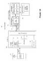
- FIGS. 1A and 1Bare block diagrams showing the controller architecture according to some embodiments.
- FIG. 2is a block diagram illustrating the command processing components between the controller and the bridge device according to one embodiment.
- FIG. 3is a block diagram showing an example of detailed error reporting according to one embodiment.
- FIG. 4is a block diagram showing another example of detailed error reporting according to another embodiment.
- FIG. 5is a combined block and flow diagram that illustrates the error reporting for a read operation according to one embodiment.
- FIG. 6is a combined block and flow diagram that illustrates the error reporting for a write operation according to one embodiment.
- Error reporting in common high-level protocolstypically reports only the first encountered point of failure. For example, in HDD, the error reporting may report that a read failed at sector X, the first point of failure, but may provide no additional information about any errors that may have been encountered elsewhere in the read.
- the commonly used ONFIOpen NAND interface
- ONFIalso has limited ability to perform queued operation. It has the active operation and the next/“cached” operation. Based on this arrangement it may be possible to detect which of the two operations failed, though involvement from a controller may be necessary. For example, current implementations of ONFI provide a status per operation and the controller may need to retrieve such status after each operation to determine whether an error has occurred. However, the situation becomes more complicated when there are multiple ONFI devices (dies) involved (e.g., 8 or more), each with two planes and cached operations that are all accessed concurrently.
- Embodiments of the inventionare directed to providing detailed error reporting of data operations performed on a NVM storage device.
- a controllerinterfaces with a NVM storage device including NVM storage coupled with a bridge.
- the controlleris provided physical, page-level access to the NVM via the bridge, and the bridge provides detailed error reporting of the data operations that the bridge performs on the NVM on behalf of the controller.
- the bridgemay provide page level reporting indicating which page(s) failed during a read operation.
- Detailed error reportingallows the controller to better understand the failures that occurred in a data access operation in the NVM. It also enables the controller to manage the flash media at the physical page/block level and provides the controller an efficient way to discover errors since the controller does not need to locate individual errors with repeated failed operations.
- FIG. 1Ashows a controller-bridge architecture in accordance with some embodiments.
- Thisis one example architecture in which the detailed error reporting mechanisms can be implemented.
- Those skilled in the artwill recognize that other equivalent or similar setups can be used.
- the description belowdiscusses standardized interfaces such as PCIe and ONFI, other similar standardized and/or proprietary interfaces can be used and/be adapted for this purpose.
- the example architecture belowincludes details related to various portions to the architecture, they should not be construed as being required and may be omitted in some embodiments.
- the detailed error reporting mechanismsmay be implemented without the various queuing mechanisms described below.
- a solid-state non-volatile storage system 120is connected to a host system 110 .
- the host system 110communicates with the non-volatile storage system 120 using a storage interface 112 .
- the host's storage interface 112can communicate with the non-volatile storage system 120 using any known communication protocol, such as SATA, SCSI, SAS, USB, Fibre Channel, PCIe, eMMC, etc.
- the non-volatile storage system 120includes a controller 130 and a NVM storage module 150 .
- the controller 130in one embodiment communicates with a bridge device 152 within the NVM storage module 150 via a high level interface such as PCIe (through bus logic/interface 140 ).
- PCIeis used in one embodiment as it defines a rich packet based routing and Quality of Service (QoS) infrastructure and provides a high speed interface.
- the controllermay include a processor 136 to control data functions, and the core may be coupled with static memory 132 and dynamic memory 134 .
- the controller 130may also include a data path 138 for processing/transferring data related to data access commands from the host system 110 .
- the controller 130is implemented on a SoC (System on Chip), though those skilled in the art will recognize that other hardware/firmware implementations are possible.
- SoCSystem on Chip
- the use of PCIemeans that the address range assigned to a device function is used for packet routing both on the fabric and within the device.
- the PCIe transaction layerdelivers packets to an internal register interface that is read by firmware. Advanced devices often direct incoming packets to internal RAM or hardware acceleration modules.
- the bridge device 152in one embodiment comprises bus logic/interface 154 for communicating with the bus logic/interface 140 (on the controller 130 ) over the high level interface bus.
- the bridge device 152includes a low level interface 158 such as ONFI for communicating with the NVM storage 160 (e.g., NAND), which may include a number of storage devices such as flash dies 162 , 164 , 166 , and 168 .
- ONFIis depicted in this embodiment, other suitable flash memory interfaces may be used.
- the bridgemay use a different interface such as Toggle or a proprietary interface to communicate with the NVM storage 160 , or send direct commands to the storage.
- the architecturereduces latency and addresses the various design constraints while allowing the controller and bridge designers to optimize their respective portions of the architecture.
- the controlleris responsible for block level management, parity stripe layout, garbage collection, wear leveling, handling read disturb and error recovery.
- the bridge devicemanages the raw NVM flash interface. It may also provide one or more of: command queuing, error correction, XOR parity accumulator, data protection and enhances block endurance.
- the interface between the bridge and the controllerin one embodiment is a lightweight PCIe-based data and management interface. The controller uses the interface control command to configure the bridge and data commands to access the NVM media.
- controlleruses physical page addressing instead of a logical one that is common in existing controller-bridge design.
- the bridgecan identify the relationship between pages, blocks, planes, and dies. This gives the controller the greatest flexibility for creating RAID stripe layout, performing data moves, and handling bad blocks. These details are abstracted from the bridge.
- direct addressingthe controller simply provides a set of direct page addresses in the command header to the bridge.
- the pagesare not necessarily sequential or even in the same block. In most cases, the controller will access pages spread across multiple planes and multiple dies in order to maximize concurrent hardware access. Additional details related to the above described controller architecture can be found in application Ser. No.
- FIG. 1Bshows the use of the controller architecture in a hybrid drive 122 , which in addition to the NVM and bridge components described above, includes a magnetic storage module 180 which has a magnetic media 184 such as a rotating hard disk drive (HDD).
- the controller 130 in this embodimentwould thus manage data accesses to both the NVM storage module 150 and magnetic storage module 180 .
- a different interface than interface 140(which connects to the NVM) may be used to connect the controller 130 to the magnetic storage module 180 .
- a hybrid drivetypically includes an SSD that has its own internal controller that has a mapping table to address the NVM within the SSD. While the HDD portion of the hybrid is typically addressed directly, the hybrid controller uses a special mapping table to determine whether data is in the SSD or the HDD. The use of this special mapping table along with the internal SSD mapping table introduces duplicate overhead in cases where data is accessed in the SSD portion of the hybrid, since there are two mapping tables and there is significant cost associated with maintaining each table.
- controller 130 in the present architecturemanages the NVM at both the block and page levels and the magnetic media, it can provide uniformed address management across the flash and magnetic media in a single location. Hence there is no need to have the two tables noted above. This has the advantages of reducing duplicative table lookups and all the associated costs/complexities related to maintaining separate mapping tables. Direct page addressing is used in the unified mapping scheme.
- the NVMcould still provide effective performance enhancement even when it has a large amount of bad blocks (e.g., 50%).
- the controlleralso has efficient address gap handling capability (on gaps caused by the bad blocks).
- the unified addressing schemedoes not necessarily require a bridge to work with the controller.
- the controllercan potentially use a raw NVM interface (e.g., ONFI) to access the NVM.
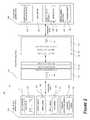
- FIG. 2is a block diagram illustrating the command processing components between the controller and the bridge device according to one embodiment.
- both the controller and the bridgeimplement its own address spaces ( 210 , 250 ) in their respective device memories that can be addressed by the other device. Messages are communicated by writing to queues located within certain addresses within the address spaces, and the addresses are stored in the configuration and status registers 252 in one embodiment. The use of individual queues to handle data access commands and communications between the controller and the bridge will be further described below.
- the controllersends data access commands to a command queue 262 in the bridge device. This is performed by the controller sending data command messages to the bridge (by writing to the command queue BAR (base address register)).
- the command queuehas room for sixteen messages, though the number of messages can vary in other embodiments.
- the command queuecan be implemented in a number of ways. One option is full hardware automation where the controller simply writes to a fixed offset. Alternately it can be implemented in memory using a ring buffer or an array based linked list. In one embodiment, the implementation must allow for efficient insertion and notification with minimal bus traffic.
- the controllerknows the current queue depth based on the number of status responses the bridge has sent back (e.g., a message to the controller's completion queue indicating completion of a command). Note that the data commands are much smaller than the actual data. A given record slot in the queue is considered available once the bridge sends back a completion status or an error report.
- the bridge side 250also implements configuration and status registers (CSR) 252 , along with an admin queue 258 for receiving, from the controller, command messages related to operation of the command queue (e.g., a message for pausing the command queue) or administrative messages concerning the bridge's operation in general.
- CSRconfiguration and status registers
- the admin queue 258may be implemented in a fashion that is similar to the command queue, such as through full hardware automation or ring buffer. Also, like the command queue, the admin queue may be configured for efficient insertion and notification with minimal bus traffic. Like the command queue, the controller can derive the current queue depth and available slots based on responses from the bridge.
- the status queuesinclude an error queue 218 , an information queue 222 , and a command completion queue 226 . These queues are responsible for receiving messages from the bridge regarding command processing, as well as current status of the bridge and the NVM.
- the controllerimplements three status queues to simplify command transactions.
- the bridgeuses the completion queue 226 to indicate when it has successfully completed one or more commands.
- the info queue 222is used for non-critical information such as health reports.
- the error queue 218allows the bridge to send detailed reports when one or more command fails.
- the controller and the bridgemay use an interrupt based system whereby the bridge would send an interrupt when it wishes to communicate with the controller. The controller may then check a message stored on the bridge side.
- PCIe protocol stack 230which includes a number of layers on both sides, including a transactional layer ( 232 , 242 ), a data link layer ( 234 , 240 ), and physical layer ( 236 , 238 ). While PCIe is used in this disclosure to illustrate the operation of the controller and the bridge, other similar standards can be used as well.
- the PCIe transaction layerassigns transmit credits based on how much room is left in its Virtual Channel (VC) buffer space.
- VCVirtual Channel
- devicesmust implement VC0, though some devices implement additional VC to ensure high priority messages have dedicated resources.
- Packetsare directed to the appropriated VC based on their Traffic Class (TC).
- TCTraffic Class
- the TCis also used to determine priority when packets are flowing over the PCIe fabric. Higher TC packets are generally given priority by the root complex, switches and end-devices.
- the controlleris designed to operate using only VC0.
- the bridgemay implement additional VC, it must be configurable so that it can operate in single VC mode.
- the messages communicated between the controller and the bridgewill be better understood in view of the following brief description of the data processing flow.
- the controllermay first send a command message to the bridge's command queue. Once the bridge processes the command message, it will read the requested data from the NVM and send the read data back to a corresponding data port on the controller side. This action triggers the data path on the controller, which leads to the data being sent back to the host.
- the controllermay first send a command message to the bridge's command queue. Once the bridge processes the command message, it will read from a corresponding data port on the controller side. This action triggers the data path on the controller, which leads to the write data being sent from a buffer in the controller to the bridge for writing to the NVM.
- the controllerin one embodiment communicates with the bridge using three message types of increasing priority: data to be written to the NVM for write commands (0), messages for the bridge's command queue (1), and messages for the bridge's admin queue (2).
- data to be written to the NVMfor write commands (0)
- messages for the bridge's command queue (1)messages for the bridge's admin queue (2).
- prioritiesmay be assigned to these messages, and the messages could be combined into fewer types or divided into more types depending on the implementation.
- the controllerunder normal conditions, sends a steady stream of data packets to the bridge.
- the bridgeinteracts with the controller using its own set of prioritized message types (listed here in increasing priority): data read from the NVM for read commands (0), messages for the controller's completion/info queues (1), and messages for the controller's error queue (2).
- prioritized message typeslisted here in increasing priority: data read from the NVM for read commands (0), messages for the controller's completion/info queues (1), and messages for the controller's error queue (2).
- prioritiesmay be assigned to these messages, and the messages could be combined into fewer types or divided into more types depending on the implementation.
- a read or write by the bridge to a data port in the controllerautomatically triggers the data path in the controller.
- the bridgeuses the completion queue 226 to notify the controller when commands have completed successfully.
- non-critical messagesare sent to the info queue 222 while detailed error reports are sent to the error queue 218 .
- these queuesmay be combined into fewer queues (with different message types being distinguished by special flags or implied address values) or separated into more queues (e.g., different error queues for different types of error or different info queues for different types of information returned from the bridge).
- PCIe protocol stackmay be replaced with the appropriate stacks/layers of that interface.
- eMMCequivalent standardized interfaces
- a custom/proprietary interfacemay be used to handle communications between the controller and the bridge.
- the bridgesupports page-level error reporting.
- the bridgemay return a message to the controller including the following: Page 1: success; Page 2: failure; Page 3: success, and so on.
- Page 1success
- Page 2failure
- Page 3success
- the controlleris able to know exactly where the failure occurred and can potentially recover data with around the range(s) of failure. Since failures tend to cluster, this also enables the controller to detect errors sooner compared to prior implementations that usually only report the first point of failure.
- the detailed error reportingenables the controller to obtain discontinuous ranges of data on reads, with “good” data being retrieved by the bridge from locations where the read was performed successfully even though some errors were encountered in locations within the range of the read operation. This can be done regardless of whether physical or logical addressing is used.
- This conceptwill be further described in FIG. 5 .
- On writescommon implementations hide errors through indirection (i.e., program errors typically lead to attempts to re-program the same data at different physical addresses), and thus sometimes no error report is generated based on that first failure if a subsequent attempt is successful. In contrast, in some embodiments of the invention, detailed write errors are reported as well. This concept will be further described in FIG. 6 .
- the controllerIn both reads and writes, the controller is able to know exactly where the failures occurred. This supports the controller's ability to manage how the media is used at the physical page/block level.
- detailed error reportingcan be provided on erase operations as well.
- the detailed error reportingmay be used to report errors deliberately injected by the bridge under the controller's instruction for testing purposes. These injected errors are further described in application entitled “SYSTEMS AND METHODS FOR ERROR INJECTION IN DATA STORAGE SYSTEMS,” application Ser. No. 13/226,416, filed Sep. 6, 2011, the disclosure of which is hereby incorporated by reference.
- the report provided per commandincludes the command ID and tag in the error report. Commands that affect multiple pages log the actions that were taken on each page. In one embodiment, error reports are sent by the bridge to the error queue in the controller.
- the bridgesupports at least the following ten error codes:
- Page UncorrectableThe page has an uncorrectable read error and cannot be read.
- the bridge and the controllerare configured to have the following behaviors upon encountering errors. There are external error behavior and internal error behavior. External error behavior is configured as follows in one embodiment.
- the controllergenerally sends data commands that result in some bus activity.
- the bridgeencounters a media error while processing a regular read or write command, it is configured to stop processing the command and generate an error report.
- a messagee.g., a command abort MSI interrupt
- itcould just throw the data away, though it is more efficient to tell the controller to stop.
- the bridgeis then free to start working on the next queued command assuming no queuing restrictions have been invoked.
- the bridgecan pause the queue until the controller restarts it.
- Internal error behavioris configured as follows according to one embodiment. Some commands from the controller may cause internal data operations that do not result in bus transfers. In the event of an error, the bridge is configured to not send an interrupt (e.g., a MSI interrupt). Instead it is configured to stop processing the command and generate an error report. It is then free to start working on the next queued command. In both the internal and external cases, as shown in the examples below, upon encountering an error the bridge in one embodiment has the option to continue through with the command. For reads, it may attempt to return valid data around the errors.
- an interrupte.g., a MSI interrupt
- FIG. 3is a block diagram showing an example 300 of detailed error reporting according to one embodiment.
- the bridgeis configured to provide the controller detailed error reporting for various data access operations.
- the reportingis page-based, that is, the bridge may provide a status for each page in which the operation is performed.
- messages 302 , 304 , and 306 to 308may be returned for an operation spanning N pages.
- Each pageis associated with a message indicating success or a message indicating a failure.
- the messagesmay be implemented as a string of bits, with the position of the bit(s) correlating to the page(s) and the value of the bit(s) correlating to the status to be returned.
- a completion messageis returned to the controller.
- the completion messagemay be returned to the controller's completion queue in one embodiment. If any error was encountered during the operation, a message is instead sent to the controller's error queue.
- the error messagedoes not necessarily indicate an uncorrectable error. Rather, it may indicate correctable errors, such that those corrected by the ECC functionality within the bridge.
- an “error” messagemay also be sent to provide the controller non-critical information related to the operation. The information may indicate that although the operation was completed, errors were encountered and corrected at particular locations. This type of error message does not interrupt the flow of the data processing and the controller may choose to process the information at a later time.
- FIG. 4is a block diagram showing another example 400 of detailed error reporting according to another embodiment. Similar to FIG. 3 , the messages are provided by the bridge to the controller to indicate success or failure at the page level. However, unlike FIG. 3 where no header information is needed to correlate the messages to the pages, the embodiment in FIG. 4 provides explicit page header information (e.g., 402 , 406 , and 412 ). For example, a message 410 includes header information 402 to indicate the page and actual status information 404 in the form of a success or error code. As with FIG. 3 , the format of the messages in FIG. 4 can be encoded in a string of bits, though those skilled in art will recognize that other formats can be used to communicate the messages shown in FIGS. 3 and 4 .
- explicit page header informatione.g. 402 , 406 , and 412 .
- a message 410includes header information 402 to indicate the page and actual status information 404 in the form of a success or error code.
- the format of the messages in FIG. 4
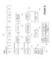
- FIG. 5is a combined block and flow diagram that illustrates the error reporting for a read operation according to one embodiment.
- FIG. 5shows a range of page addresses 500 showing the results if a read operation were to be performed. As shown, if the eight pages (P 0 -P 7 ) were read, six would be read successfully (P 0 - 2 , P 4 - 5 , and P 7 ) and two would not be read successfully (P 3 and P 6 ).
- the flow diagram of blocks 502 - 508shows a common implementation.
- a controller or bridge devicewould begin by attempting to read the pages.
- itwould encounter the failure at P 3 .
- itwould abort the read operation, and in block 508 it would report the failure of the overall read operation.
- data from P 0 -P 2the first successfully read pages before the failure, may be returned.
- the flow diagram of blocks 512 - 528illustrates the error reporting for a read according to one embodiment.
- the bridgewould begin to read the pages. It would encounter a failure at P 3 (block 514 ). However, instead of aborting, the bridge would continue to read to the end of the range for the current read operation (which is P 7 in this example). It would encounter a second failure at P 6 (block 518 ), but it would again continue until the end of the range (blocks 520 , 522 ). The bridge would then provide a detailed report about the read operation to the controller in block 524 . An example report is shown in block 526 . Then, optionally, the bridge would return data from pages where read was performed successfully in block 528 .
- the “good” data from the successfully read pagesare returned along an error report.
- the “good” data from the successfully read pagesare returned with (1) the “bad” data from the unsuccessfully pages or (2) a filler data pattern in place of the “bad” data at the pages where the read was unsuccessful. It is noted that in some embodiments aborting at the first point of failure is an option, as discussed above. In that case, an error status message would be sent to the controller notifying that the operation was aborted. Such an error report would still be useful in many circumstances.
- the resulting error reportcould still provide error/success status on the locations worked on by the individual sub-operations within the current group of parallel sub-operations when the abort signal is sent. Due to the parallel nature of the sub-operations and potential lag time between the sending of the abort signal to the actual stoppage of the sub-operations, additional errors may be reported in that current group beyond that which triggered the abort. This information may be in addition to status from locations worked on by prior groups of parallel sub-operations for this read operation, if there were any. Additional status may also be provided for those locations (e.g., pages) that were not operated on due to the abort.
- FIG. 6is a combined block and flow diagram that illustrates the error reporting for a write operation according to one embodiment.
- FIG. 6shows a range of page addresses 600 showing the results if a write operation were to be performed. As shown, if the eight pages (P 0 -P 7 ) were written, six would be written successfully (P 0 - 2 , P 4 - 5 , and P 7 ) and two would not be written successfully (P 3 and P 6 ).
- the flow diagram of blocks 602 - 614illustrates the error reporting for a write according to one embodiment.
- the bridgewould begin to write the pages. It would encounter a failure at P 3 (block 604 ). However, instead of aborting, the bridge would continue to write to the end of the range for the current write operation (which is P 7 in this example). It would encounter a second failure at P 6 (block 608 ), but it would again continue until the end of the range (blocks 610 , 612 ). The bridge would then provide a detailed report about the write operation to the controller in 614 . An example report is shown in block 616 . It is noted that in some embodiments aborting at the first point of failure is an option, as discussed above.
- an error status messagewould be sent to the controller notifying that the operation was aborted.
- the reportmay include error/success indications for the various locations worked on by the parallel sub-operations.
- non-volatile memorytypically refers to solid-state memory such as NAND flash.
- systems and methods of this disclosuremay also be useful in more conventional hard drives and hybrid drives including both solid-state and hard drive components.
- certain internal operationsare referred to which typically are associated with solid-state drives, such as “wear leveling” and “garbage collection,” analogous operations for hard drives can also take advantage of some embodiments of this disclosure.
- Solid-state memorymay comprise a wide variety of technologies, such as flash integrated circuits, Chalcogenide RAM (C-RAM), Phase Change Memory (PC-RAM or PRAM), Programmable Metallization Cell RAM (PMC-RAM or PMCm), Ovonic Unified Memory (OUM), Resistance RAM (RRAM), NAND memory, NOR memory, EEPROM, Ferroelectric Memory (FeRAM), or other discrete NVM (non-volatile memory) chips.
- the solid-state storage devicese.g., dies
- Other forms of storagee.g., battery backed-up volatile DRAM or SRAM devices, magnetic disk drives, etc.
- FIGS. 1A , 1 B, and 2may be implemented as software and/or firmware on a processor, ASIC/FPGA, or dedicated hardware.
Landscapes
- Engineering & Computer Science (AREA)
- Theoretical Computer Science (AREA)
- Quality & Reliability (AREA)
- Physics & Mathematics (AREA)
- General Engineering & Computer Science (AREA)
- General Physics & Mathematics (AREA)
- Debugging And Monitoring (AREA)
Abstract
Description
Claims (22)
Priority Applications (1)
| Application Number | Priority Date | Filing Date | Title |
|---|---|---|---|
| US14/185,770US9058261B1 (en) | 2011-09-06 | 2014-02-20 | Systems and methods for detailed error reporting in data storage systems |
Applications Claiming Priority (2)
| Application Number | Priority Date | Filing Date | Title |
|---|---|---|---|
| US13/226,418US8713357B1 (en) | 2011-09-06 | 2011-09-06 | Systems and methods for detailed error reporting in data storage systems |
| US14/185,770US9058261B1 (en) | 2011-09-06 | 2014-02-20 | Systems and methods for detailed error reporting in data storage systems |
Related Parent Applications (1)
| Application Number | Title | Priority Date | Filing Date |
|---|---|---|---|
| US13/226,418ContinuationUS8713357B1 (en) | 2011-09-06 | 2011-09-06 | Systems and methods for detailed error reporting in data storage systems |
Publications (1)
| Publication Number | Publication Date |
|---|---|
| US9058261B1true US9058261B1 (en) | 2015-06-16 |
Family
ID=50514402
Family Applications (2)
| Application Number | Title | Priority Date | Filing Date |
|---|---|---|---|
| US13/226,418Active2032-07-05US8713357B1 (en) | 2011-09-06 | 2011-09-06 | Systems and methods for detailed error reporting in data storage systems |
| US14/185,770ActiveUS9058261B1 (en) | 2011-09-06 | 2014-02-20 | Systems and methods for detailed error reporting in data storage systems |
Family Applications Before (1)
| Application Number | Title | Priority Date | Filing Date |
|---|---|---|---|
| US13/226,418Active2032-07-05US8713357B1 (en) | 2011-09-06 | 2011-09-06 | Systems and methods for detailed error reporting in data storage systems |
Country Status (1)
| Country | Link |
|---|---|
| US (2) | US8713357B1 (en) |
Cited By (8)
| Publication number | Priority date | Publication date | Assignee | Title |
|---|---|---|---|---|
| US9268640B1 (en)* | 2013-12-20 | 2016-02-23 | Emc Corporation | Limiting data loss on parity RAID groups |
| US9529663B1 (en) | 2015-12-20 | 2016-12-27 | Apple Inc. | Detection and localization of failures in 3D NAND flash memory |
| US10248515B2 (en) | 2017-01-19 | 2019-04-02 | Apple Inc. | Identifying a failing group of memory cells in a multi-plane storage operation |
| US10755787B2 (en) | 2018-06-28 | 2020-08-25 | Apple Inc. | Efficient post programming verification in a nonvolatile memory |
| US10762967B2 (en) | 2018-06-28 | 2020-09-01 | Apple Inc. | Recovering from failure in programming a nonvolatile memory |
| US10915394B1 (en) | 2019-09-22 | 2021-02-09 | Apple Inc. | Schemes for protecting data in NVM device using small storage footprint |
| US10936455B2 (en) | 2019-02-11 | 2021-03-02 | Apple Inc. | Recovery of data failing due to impairment whose severity depends on bit-significance value |
| US11550657B1 (en) | 2021-09-01 | 2023-01-10 | Apple Inc. | Efficient programming schemes in a nonvolatile memory |
Families Citing this family (116)
| Publication number | Priority date | Publication date | Assignee | Title |
|---|---|---|---|---|
| US9176859B2 (en) | 2009-01-07 | 2015-11-03 | Siliconsystems, Inc. | Systems and methods for improving the performance of non-volatile memory operations |
| US10079048B2 (en) | 2009-03-24 | 2018-09-18 | Western Digital Technologies, Inc. | Adjusting access of non-volatile semiconductor memory based on access time |
| US9753847B2 (en) | 2009-10-27 | 2017-09-05 | Western Digital Technologies, Inc. | Non-volatile semiconductor memory segregating sequential, random, and system data to reduce garbage collection for page based mapping |
| US8782327B1 (en) | 2010-05-11 | 2014-07-15 | Western Digital Technologies, Inc. | System and method for managing execution of internal commands and host commands in a solid-state memory |
| US9026716B2 (en) | 2010-05-12 | 2015-05-05 | Western Digital Technologies, Inc. | System and method for managing garbage collection in solid-state memory |
| US8959284B1 (en) | 2010-06-28 | 2015-02-17 | Western Digital Technologies, Inc. | Disk drive steering write data to write cache based on workload |
| US9058280B1 (en) | 2010-08-13 | 2015-06-16 | Western Digital Technologies, Inc. | Hybrid drive migrating data from disk to non-volatile semiconductor memory based on accumulated access time |
| US8769190B1 (en) | 2010-09-15 | 2014-07-01 | Western Digital Technologies, Inc. | System and method for reducing contentions in solid-state memory access |
| US8788779B1 (en) | 2010-09-17 | 2014-07-22 | Western Digital Technologies, Inc. | Non-volatile storage subsystem with energy-based performance throttling |
| US9021192B1 (en) | 2010-09-21 | 2015-04-28 | Western Digital Technologies, Inc. | System and method for enhancing processing of memory access requests |
| US9164886B1 (en) | 2010-09-21 | 2015-10-20 | Western Digital Technologies, Inc. | System and method for multistage processing in a memory storage subsystem |
| US9069475B1 (en) | 2010-10-26 | 2015-06-30 | Western Digital Technologies, Inc. | Hybrid drive selectively spinning up disk when powered on |
| US8700950B1 (en) | 2011-02-11 | 2014-04-15 | Western Digital Technologies, Inc. | System and method for data error recovery in a solid state subsystem |
| US8700951B1 (en) | 2011-03-09 | 2014-04-15 | Western Digital Technologies, Inc. | System and method for improving a data redundancy scheme in a solid state subsystem with additional metadata |
| US8930647B1 (en) | 2011-04-06 | 2015-01-06 | P4tents1, LLC | Multiple class memory systems |
| US9176671B1 (en) | 2011-04-06 | 2015-11-03 | P4tents1, LLC | Fetching data between thread execution in a flash/DRAM/embedded DRAM-equipped system |
| US9158546B1 (en) | 2011-04-06 | 2015-10-13 | P4tents1, LLC | Computer program product for fetching from a first physical memory between an execution of a plurality of threads associated with a second physical memory |
| US9170744B1 (en) | 2011-04-06 | 2015-10-27 | P4tents1, LLC | Computer program product for controlling a flash/DRAM/embedded DRAM-equipped system |
| US9164679B2 (en) | 2011-04-06 | 2015-10-20 | Patents1, Llc | System, method and computer program product for multi-thread operation involving first memory of a first memory class and second memory of a second memory class |
| US9417754B2 (en) | 2011-08-05 | 2016-08-16 | P4tents1, LLC | User interface system, method, and computer program product |
| US8707104B1 (en) | 2011-09-06 | 2014-04-22 | Western Digital Technologies, Inc. | Systems and methods for error injection in data storage systems |
| US9195530B1 (en) | 2011-09-06 | 2015-11-24 | Western Digital Technologies, Inc. | Systems and methods for improved data management in data storage systems |
| US8713357B1 (en) | 2011-09-06 | 2014-04-29 | Western Digital Technologies, Inc. | Systems and methods for detailed error reporting in data storage systems |
| US8700834B2 (en) | 2011-09-06 | 2014-04-15 | Western Digital Technologies, Inc. | Systems and methods for an enhanced controller architecture in data storage systems |
| US9268701B1 (en) | 2011-11-21 | 2016-02-23 | Western Digital Technologies, Inc. | Caching of data in data storage systems by managing the size of read and write cache based on a measurement of cache reliability |
| US8959416B1 (en) | 2011-12-16 | 2015-02-17 | Western Digital Technologies, Inc. | Memory defect management using signature identification |
| US9348741B1 (en) | 2011-12-19 | 2016-05-24 | Western Digital Technologies, Inc. | Systems and methods for handling write data access requests in data storage devices |
| US9053008B1 (en) | 2012-03-26 | 2015-06-09 | Western Digital Technologies, Inc. | Systems and methods for providing inline parameter service in data storage devices |
| US9977612B1 (en) | 2012-05-11 | 2018-05-22 | Western Digital Technologies, Inc. | System data management using garbage collection and logs |
| US9170932B1 (en) | 2012-05-22 | 2015-10-27 | Western Digital Technologies, Inc. | System data storage mechanism providing coherency and segmented data loading |
| US8954653B1 (en) | 2012-06-26 | 2015-02-10 | Western Digital Technologies, Inc. | Mechanisms for efficient management of system data in data storage systems |
| US8924832B1 (en) | 2012-06-26 | 2014-12-30 | Western Digital Technologies, Inc. | Efficient error handling mechanisms in data storage systems |
| US8966343B2 (en) | 2012-08-21 | 2015-02-24 | Western Digital Technologies, Inc. | Solid-state drive retention monitor using reference blocks |
| US9489296B1 (en) | 2012-10-17 | 2016-11-08 | Western Digital Technologies, Inc. | Methods, devices and systems for hardware-based garbage collection in solid state drives |
| US8972826B2 (en) | 2012-10-24 | 2015-03-03 | Western Digital Technologies, Inc. | Adaptive error correction codes for data storage systems |
| US9177638B2 (en) | 2012-11-13 | 2015-11-03 | Western Digital Technologies, Inc. | Methods and devices for avoiding lower page corruption in data storage devices |
| US8954694B2 (en) | 2012-11-15 | 2015-02-10 | Western Digital Technologies, Inc. | Methods, data storage devices and systems for fragmented firmware table rebuild in a solid state drive |
| US9021339B2 (en) | 2012-11-29 | 2015-04-28 | Western Digital Technologies, Inc. | Data reliability schemes for data storage systems |
| US9059736B2 (en) | 2012-12-03 | 2015-06-16 | Western Digital Technologies, Inc. | Methods, solid state drive controllers and data storage devices having a runtime variable raid protection scheme |
| US9032271B2 (en) | 2012-12-07 | 2015-05-12 | Western Digital Technologies, Inc. | System and method for lower page data recovery in a solid state drive |
| US8954655B2 (en) | 2013-01-14 | 2015-02-10 | Western Digital Technologies, Inc. | Systems and methods of configuring a mode of operation in a solid-state memory |
| US8972655B2 (en) | 2013-01-21 | 2015-03-03 | Western Digital Technolgies, Inc. | Initialization of a storage device |
| US9274966B1 (en) | 2013-02-20 | 2016-03-01 | Western Digital Technologies, Inc. | Dynamically throttling host commands to disk drives |
| US9454474B2 (en) | 2013-03-05 | 2016-09-27 | Western Digital Technologies, Inc. | Methods, devices and systems for two stage power-on map rebuild with free space accounting in a solid state drive |
| US8924824B1 (en) | 2013-03-12 | 2014-12-30 | Western Digital Technologies, Inc. | Soft-decision input generation for data storage systems |
| US8990668B2 (en) | 2013-03-14 | 2015-03-24 | Western Digital Technologies, Inc. | Decoding data stored in solid-state memory |
| US9218279B2 (en) | 2013-03-15 | 2015-12-22 | Western Digital Technologies, Inc. | Atomic write command support in a solid state drive |
| US9335950B2 (en) | 2013-03-15 | 2016-05-10 | Western Digital Technologies, Inc. | Multiple stream compression and formatting of data for data storage systems |
| US9448738B2 (en) | 2013-03-15 | 2016-09-20 | Western Digital Technologies, Inc. | Compression and formatting of data for data storage systems |
| US9338927B2 (en) | 2013-05-02 | 2016-05-10 | Western Digital Technologies, Inc. | Thermal interface material pad and method of forming the same |
| US9195293B1 (en) | 2013-05-03 | 2015-11-24 | Western Digital Technologies, Inc. | User controlled data storage device power and performance settings |
| US9632926B1 (en) | 2013-05-16 | 2017-04-25 | Western Digital Technologies, Inc. | Memory unit assignment and selection for internal memory operations in data storage systems |
| US9081700B2 (en) | 2013-05-16 | 2015-07-14 | Western Digital Technologies, Inc. | High performance read-modify-write system providing line-rate merging of dataframe segments in hardware |
| US9170938B1 (en) | 2013-05-17 | 2015-10-27 | Western Digital Technologies, Inc. | Method and system for atomically writing scattered information in a solid state storage device |
| US9280200B1 (en) | 2013-05-20 | 2016-03-08 | Western Digital Technologies, Inc. | Automatic peak current throttle of tiered storage elements |
| US9740248B2 (en) | 2013-06-07 | 2017-08-22 | Western Digital Technologies, Inc. | Component placement within a solid state drive |
| US9274978B2 (en) | 2013-06-10 | 2016-03-01 | Western Digital Technologies, Inc. | Migration of encrypted data for data storage systems |
| US9436630B2 (en) | 2013-06-11 | 2016-09-06 | Western Digital Technologies, Inc. | Using dual phys to support multiple PCIe link widths |
| US9830257B1 (en) | 2013-06-12 | 2017-11-28 | Western Digital Technologies, Inc. | Fast saving of data during power interruption in data storage systems |
| US9665501B1 (en) | 2013-06-18 | 2017-05-30 | Western Digital Technologies, Inc. | Self-encrypting data storage device supporting object-level encryption |
| US9304560B2 (en) | 2013-06-19 | 2016-04-05 | Western Digital Technologies, Inc. | Backup power for reducing host current transients |
| US9208101B2 (en) | 2013-06-26 | 2015-12-08 | Western Digital Technologies, Inc. | Virtual NAND capacity extension in a hybrid drive |
| US9583153B1 (en) | 2013-06-28 | 2017-02-28 | Western Digital Technologies, Inc. | Memory card placement within a solid state drive |
| US9042197B2 (en) | 2013-07-23 | 2015-05-26 | Western Digital Technologies, Inc. | Power fail protection and recovery using low power states in a data storage device/system |
| US9141176B1 (en) | 2013-07-29 | 2015-09-22 | Western Digital Technologies, Inc. | Power management for data storage device |
| US9442668B1 (en) | 2013-08-29 | 2016-09-13 | Western Digital Technologies, Inc. | Adaptive power management control with performance feedback |
| US9263136B1 (en) | 2013-09-04 | 2016-02-16 | Western Digital Technologies, Inc. | Data retention flags in solid-state drives |
| US9304709B2 (en) | 2013-09-06 | 2016-04-05 | Western Digital Technologies, Inc. | High performance system providing selective merging of dataframe segments in hardware |
| US10444998B1 (en) | 2013-10-24 | 2019-10-15 | Western Digital Technologies, Inc. | Data storage device providing data maintenance services |
| US9007841B1 (en) | 2013-10-24 | 2015-04-14 | Western Digital Technologies, Inc. | Programming scheme for improved voltage distribution in solid-state memory |
| US9330143B2 (en) | 2013-10-24 | 2016-05-03 | Western Digital Technologies, Inc. | Data storage device supporting accelerated database operations |
| US8917471B1 (en) | 2013-10-29 | 2014-12-23 | Western Digital Technologies, Inc. | Power management for data storage device |
| US9323467B2 (en) | 2013-10-29 | 2016-04-26 | Western Digital Technologies, Inc. | Data storage device startup |
| US9286176B1 (en) | 2013-11-08 | 2016-03-15 | Western Digital Technologies, Inc. | Selective skipping of blocks in an SSD |
| US9270296B1 (en) | 2013-11-13 | 2016-02-23 | Western Digital Technologies, Inc. | Method and system for soft decoding through single read |
| US9529710B1 (en) | 2013-12-06 | 2016-12-27 | Western Digital Technologies, Inc. | Interleaved channels in a solid-state drive |
| US10140067B1 (en) | 2013-12-19 | 2018-11-27 | Western Digital Technologies, Inc. | Data management for data storage device with multiple types of non-volatile memory media |
| US9036283B1 (en) | 2014-01-22 | 2015-05-19 | Western Digital Technologies, Inc. | Data storage device with selective write to a first storage media or a second storage media |
| US9337864B1 (en) | 2014-01-29 | 2016-05-10 | Western Digital Technologies, Inc. | Non-binary LDPC decoder using binary subgroup processing |
| US9250994B1 (en) | 2014-02-05 | 2016-02-02 | Western Digital Technologies, Inc. | Non-binary low-density parity check (LDPC) decoding using trellis maximization |
| US9384088B1 (en) | 2014-02-24 | 2016-07-05 | Western Digital Technologies, Inc. | Double writing map table entries in a data storage system to guard against silent corruption |
| US9354955B1 (en) | 2014-03-19 | 2016-05-31 | Western Digital Technologies, Inc. | Partial garbage collection for fast error handling and optimized garbage collection for the invisible band |
| US9348520B2 (en) | 2014-03-24 | 2016-05-24 | Western Digital Technologies, Inc. | Lifetime extension of non-volatile semiconductor memory for data storage device |
| US9268487B2 (en) | 2014-03-24 | 2016-02-23 | Western Digital Technologies, Inc. | Method and apparatus for restricting writes to solid state memory when an end-of life condition is reached |
| US9448742B2 (en) | 2014-03-27 | 2016-09-20 | Western Digital Technologies, Inc. | Communication between a host and a secondary storage device |
| US9564212B2 (en) | 2014-05-06 | 2017-02-07 | Western Digital Technologies, Inc. | Solid-state memory corruption mitigation |
| US9690696B1 (en) | 2014-05-14 | 2017-06-27 | Western Digital Technologies, Inc. | Lifetime extension of memory for data storage system |
| US9472222B2 (en) | 2014-05-16 | 2016-10-18 | Western Digital Technologies, Inc. | Vibration mitigation for a data storage device |
| US9275741B1 (en) | 2014-09-10 | 2016-03-01 | Western Digital Technologies, Inc. | Temperature compensation management in solid-state memory |
| US9418699B1 (en) | 2014-10-09 | 2016-08-16 | Western Digital Technologies, Inc. | Management of sequentially written data |
| US9405356B1 (en)* | 2014-10-21 | 2016-08-02 | Western Digital Technologies, Inc. | Temperature compensation in data storage device |
| US9823859B2 (en) | 2014-11-06 | 2017-11-21 | Western Digital Technologies, Inc. | Mechanical shock mitigation for data storage |
| US9857995B1 (en) | 2015-03-09 | 2018-01-02 | Western Digital Technologies, Inc. | Data storage device and method providing non-volatile memory buffer for real-time primary non-volatile memory protection |
| US10078448B2 (en) | 2015-07-08 | 2018-09-18 | Samsung Electronics Co., Ltd. | Electronic devices and memory management methods thereof |
| US9785563B1 (en) | 2015-08-13 | 2017-10-10 | Western Digital Technologies, Inc. | Read command processing for data storage system based on previous writes |
| US9668337B2 (en) | 2015-09-08 | 2017-05-30 | Western Digital Technologies, Inc. | Temperature management in data storage devices |
| US9727261B2 (en) | 2015-09-24 | 2017-08-08 | Western Digital Technologies, Inc. | Weighted programming patterns in solid-state data storage systems |
| US9836232B1 (en) | 2015-09-30 | 2017-12-05 | Western Digital Technologies, Inc. | Data storage device and method for using secondary non-volatile memory for temporary metadata storage |
| US10013174B2 (en) | 2015-09-30 | 2018-07-03 | Western Digital Technologies, Inc. | Mapping system selection for data storage device |
| US9620226B1 (en) | 2015-10-30 | 2017-04-11 | Western Digital Technologies, Inc. | Data retention charge loss and read disturb compensation in solid-state data storage systems |
| US10126981B1 (en) | 2015-12-14 | 2018-11-13 | Western Digital Technologies, Inc. | Tiered storage using storage class memory |
| US10387303B2 (en) | 2016-08-16 | 2019-08-20 | Western Digital Technologies, Inc. | Non-volatile storage system with compute engine to accelerate big data applications |
| US10459644B2 (en) | 2016-10-28 | 2019-10-29 | Western Digital Techologies, Inc. | Non-volatile storage system with integrated compute engine and optimized use of local fast memory |
| US10565123B2 (en) | 2017-04-10 | 2020-02-18 | Western Digital Technologies, Inc. | Hybrid logical to physical address translation for non-volatile storage devices with integrated compute module |
| US10540219B2 (en) | 2017-09-13 | 2020-01-21 | Toshiba Memory Corporation | Reset and error handling in application specific integrated circuits |
| US10528414B2 (en)* | 2017-09-13 | 2020-01-07 | Toshiba Memory Corporation | Centralized error handling in application specific integrated circuits |
| US10353606B2 (en) | 2017-10-12 | 2019-07-16 | International Business Machines Corporation | Partial data replay in a distributed memory buffer system |
| US10956071B2 (en) | 2018-10-01 | 2021-03-23 | Western Digital Technologies, Inc. | Container key value store for data storage devices |
| US10769062B2 (en) | 2018-10-01 | 2020-09-08 | Western Digital Technologies, Inc. | Fine granularity translation layer for data storage devices |
| US10740231B2 (en) | 2018-11-20 | 2020-08-11 | Western Digital Technologies, Inc. | Data access in data storage device including storage class memory |
| US11175979B2 (en)* | 2019-08-06 | 2021-11-16 | Micron Technology, Inc. | Prioritization of error control operations at a memory sub-system |
| US11016905B1 (en) | 2019-11-13 | 2021-05-25 | Western Digital Technologies, Inc. | Storage class memory access |
| US20210157519A1 (en)* | 2019-11-26 | 2021-05-27 | Microsoft Technology Licensing, Llc | Solid-state drive (ssd) with a storage controller employing differential two-wire serial buses to access flash memory |
| US11249921B2 (en) | 2020-05-06 | 2022-02-15 | Western Digital Technologies, Inc. | Page modification encoding and caching |
| US11947995B2 (en)* | 2020-05-19 | 2024-04-02 | Intel Corporation | End-to-end data protection for far memory data transfer from host to media |
| TWI859855B (en)* | 2023-05-12 | 2024-10-21 | 慧榮科技股份有限公司 | Bridge device and method for transferring command and data |
Citations (154)
| Publication number | Priority date | Publication date | Assignee | Title |
|---|---|---|---|---|
| US6148354A (en) | 1999-04-05 | 2000-11-14 | M-Systems Flash Disk Pioneers Ltd. | Architecture for a universal serial bus-based PC flash disk |
| US6182248B1 (en) | 1998-04-07 | 2001-01-30 | International Business Machines Corporation | Method and tool for computer bus fault isolation and recovery design verification |
| US6304984B1 (en) | 1998-09-29 | 2001-10-16 | International Business Machines Corporation | Method and system for injecting errors to a device within a computer system |
| US20020053010A1 (en) | 2000-01-25 | 2002-05-02 | Piccirillo Gary J. | Method for supporting multi-level stripping of non-homogeneous memory to maximize concurrency |
| US6519718B1 (en) | 2000-02-18 | 2003-02-11 | International Business Machines Corporation | Method and apparatus implementing error injection for PCI bridges |
| US20030165076A1 (en) | 2001-09-28 | 2003-09-04 | Gorobets Sergey Anatolievich | Method of writing data to non-volatile memory |
| US20030172261A1 (en) | 2002-03-08 | 2003-09-11 | Seok-Heon Lee | System boot using NAND flash memory and method thereof |
| US6735661B2 (en) | 2000-06-27 | 2004-05-11 | Koninklijke Philips Electronics N.V. | Integrated circuit with flash memory including dedicated flash bus and flash bridge |
| US6785767B2 (en) | 2000-12-26 | 2004-08-31 | Intel Corporation | Hybrid mass storage system and method with two different types of storage medium |
| US6856556B1 (en) | 2003-04-03 | 2005-02-15 | Siliconsystems, Inc. | Storage subsystem with embedded circuit for protecting against anomalies in power signal from host |
| US20050160217A1 (en) | 2003-12-31 | 2005-07-21 | Gonzalez Carlos J. | Flash memory system startup operation |
| US20050223373A1 (en) | 2004-04-05 | 2005-10-06 | Dell Products L.P. | Method for updating the firmware of a device |
| US20050251617A1 (en) | 2004-05-07 | 2005-11-10 | Sinclair Alan W | Hybrid non-volatile memory system |
| US6988175B2 (en)* | 2003-06-30 | 2006-01-17 | M-Systems Flash Disk Pioneers Ltd. | Flash memory management method that is resistant to data corruption by power loss |
| US7103684B2 (en) | 2003-12-02 | 2006-09-05 | Super Talent Electronics, Inc. | Single-chip USB controller reading power-on boot code from integrated flash memory for user storage |
| US7127549B2 (en) | 2004-02-04 | 2006-10-24 | Sandisk Corporation | Disk acceleration using first and second storage devices |
| US20060248387A1 (en) | 2005-04-15 | 2006-11-02 | Microsoft Corporation | In-line non volatile memory disk read cache and write buffer |
| US7136973B2 (en) | 2004-02-04 | 2006-11-14 | Sandisk Corporation | Dual media storage device |
| US20070038901A1 (en)* | 2003-02-07 | 2007-02-15 | Shigemasa Shiota | Nonvolatile memory system |
| US20070180328A1 (en) | 2006-01-27 | 2007-08-02 | Cornwell Michael J | Monitoring health of non-volatile memory |
| US20070190328A1 (en) | 2005-12-16 | 2007-08-16 | Ingenia Holdings (U.K.) Limited | Modification |
| US20070220202A1 (en) | 2004-06-10 | 2007-09-20 | Sehat Sutardja | Adaptive storage system including hard disk drive with flash interface |
| US20070245092A1 (en) | 2006-04-12 | 2007-10-18 | Hsin-Chung Yeh | Non-volatile memory sharing apparatus for multiple processors and method thereof |
| US20070288683A1 (en) | 2006-06-07 | 2007-12-13 | Microsoft Corporation | Hybrid memory device with single interface |
| US20070288692A1 (en) | 2006-06-08 | 2007-12-13 | Bitmicro Networks, Inc. | Hybrid Multi-Tiered Caching Storage System |
| US20080040531A1 (en)* | 2006-08-14 | 2008-02-14 | Dennis Anderson | Data storage device |
| US20080192928A1 (en)* | 2000-01-06 | 2008-08-14 | Super Talent Electronics, Inc. | Portable Electronic Storage Devices with Hardware Security Based on Advanced Encryption Standard |
| US20080215808A1 (en) | 2004-06-21 | 2008-09-04 | Dot Hill Systems Corporation | Raid controller using capacitor energy source to flush volatile cache data to non-volatile memory during main power outage |
| US7430136B2 (en) | 2004-11-30 | 2008-09-30 | Siliconsystems, Inc. | Purge operations for solid-state storage devices |
| US20080250270A1 (en)* | 2007-03-29 | 2008-10-09 | Bennett Jon C R | Memory management system and method |
| US7447807B1 (en) | 2006-06-30 | 2008-11-04 | Siliconsystems, Inc. | Systems and methods for storing data in segments of a storage subsystem |
| US7460394B2 (en) | 2006-05-18 | 2008-12-02 | Infineon Technologies Ag | Phase change memory having temperature budget sensor |
| US20090013233A1 (en)* | 2007-07-06 | 2009-01-08 | Micron Technology, Inc. | Error recovery storage along a nand-flash string |
| US20090024793A1 (en) | 2007-07-17 | 2009-01-22 | Fontenot Nathan D | Method and apparatus for managing data in a hybrid drive system |
| US20090037652A1 (en) | 2003-12-02 | 2009-02-05 | Super Talent Electronics Inc. | Command Queuing Smart Storage Transfer Manager for Striping Data to Raw-NAND Flash Modules |
| US20090063730A1 (en) | 2007-08-31 | 2009-03-05 | Gower Kevin C | System for Supporting Partial Cache Line Write Operations to a Memory Module to Reduce Write Data Traffic on a Memory Channel |
| US7509441B1 (en) | 2006-06-30 | 2009-03-24 | Siliconsystems, Inc. | Systems and methods for segmenting and protecting a storage subsystem |
| US20090158124A1 (en)* | 2006-05-18 | 2009-06-18 | Buffalo Inc. | Data storage apparatus and data storage method |
| US20090172257A1 (en) | 2007-12-27 | 2009-07-02 | Pliant Technology, Inc | System and method for performing host initiated mass storage commands using a hierarchy of data structures |
| US20090240873A1 (en) | 2003-12-02 | 2009-09-24 | Super Talent Electronics Inc. | Multi-Level Striping and Truncation Channel-Equalization for Flash-Memory System |
| US7596643B2 (en) | 2007-02-07 | 2009-09-29 | Siliconsystems, Inc. | Storage subsystem with configurable buffer |
| US20090282305A1 (en)* | 2008-05-09 | 2009-11-12 | A-Data Technology Co., Ltd. | Storage system with data recovery function and method thereof |
| US7623401B2 (en) | 2006-10-06 | 2009-11-24 | Qimonda North America Corp. | Semiconductor device including multi-bit memory cells and a temperature budget sensor |
| US7631245B2 (en) | 2005-09-26 | 2009-12-08 | Sandisk Il Ltd. | NAND flash memory controller exporting a NAND interface |
| US20090313411A1 (en) | 2008-06-12 | 2009-12-17 | Stenfort Ross J | Apparatus and methods crc error injection in a storage system |
| US7653778B2 (en) | 2006-05-08 | 2010-01-26 | Siliconsystems, Inc. | Systems and methods for measuring the useful life of solid-state storage devices |
| US20100023800A1 (en)* | 2005-09-26 | 2010-01-28 | Eliyahou Harari | NAND Flash Memory Controller Exporting a NAND Interface |
| US20100037012A1 (en) | 2007-12-28 | 2010-02-11 | Hirokuni Yano | Semiconductor Storage Device, Method of Controlling the Same, Controller and Information Processing Apparatus |
| US7685337B2 (en) | 2007-05-24 | 2010-03-23 | Siliconsystems, Inc. | Solid state storage subsystem for embedded applications |
| US7685374B2 (en) | 2007-07-26 | 2010-03-23 | Siliconsystems, Inc. | Multi-interface and multi-bus structured solid-state storage subsystem |
| US7685338B2 (en) | 2007-05-24 | 2010-03-23 | Siliconsystems, Inc. | Solid state storage subsystem for embedded applications |
| US20100088459A1 (en) | 2008-10-06 | 2010-04-08 | Siamak Arya | Improved Hybrid Drive |
| US20100100675A1 (en) | 2008-10-17 | 2010-04-22 | Seagate Technology Llc | System and method for managing storage device caching |
| US20100122022A1 (en)* | 2008-05-27 | 2010-05-13 | Initio Corporation | Ssd with improved bad block managment |
| US7733712B1 (en) | 2008-05-20 | 2010-06-08 | Siliconsystems, Inc. | Storage subsystem with embedded circuit for protecting against anomalies in power signal from host |
| US20100174851A1 (en) | 2009-01-08 | 2010-07-08 | Micron Technology, Inc. | Memory system controller |
| US20100174849A1 (en) | 2009-01-07 | 2010-07-08 | Siliconsystems, Inc. | Systems and methods for improving the performance of non-volatile memory operations |
| US20100180182A1 (en)* | 2009-01-09 | 2010-07-15 | Seagate Technology Llc | Data memory device and controller with interface error detection and handling logic |
| US7765373B1 (en) | 2006-06-27 | 2010-07-27 | Siliconsystems, Inc. | System for controlling use of a solid-state storage subsystem |
| US20100205517A1 (en)* | 2009-02-10 | 2010-08-12 | Doogie Lee | Solid State Disk Device and Program Fail Processing Method Thereof |
| US20100250793A1 (en) | 2009-03-24 | 2010-09-30 | Western Digital Technologies, Inc. | Adjusting access of non-volatile semiconductor memory based on access time |
| US20100268874A1 (en) | 2006-06-30 | 2010-10-21 | Mosaid Technologies Incorporated | Method of configuring non-volatile memory for a hybrid disk drive |
| US20100281342A1 (en)* | 2009-04-30 | 2010-11-04 | Samsung Electronics Co., Ltd. | Memory controller and memory system |
| US20100325352A1 (en) | 2009-06-19 | 2010-12-23 | Ocz Technology Group, Inc. | Hierarchically structured mass storage device and method |
| US20100327923A1 (en) | 2009-06-29 | 2010-12-30 | Mosaid Technologies Incorporated | Bridging device having a frequency configurable clock domain |
| US20110035540A1 (en) | 2009-08-10 | 2011-02-10 | Adtron, Inc. | Flash blade system architecture and method |
| US20110040924A1 (en)* | 2009-08-11 | 2011-02-17 | Selinger Robert D | Controller and Method for Detecting a Transmission Error Over a NAND Interface Using Error Detection Code |
| WO2011019596A2 (en) | 2009-08-11 | 2011-02-17 | Sandisk Corporation | Controller and method for interfacing between a host controller in a host and a flash memory device |
| US20110082985A1 (en) | 2009-10-05 | 2011-04-07 | Seagate Technology Llc | Data management in a data storage system |
| US20110099323A1 (en) | 2009-10-27 | 2011-04-28 | Western Digital Technologies, Inc. | Non-volatile semiconductor memory segregating sequential, random, and system data to reduce garbage collection for page based mapping |
| US20110107076A1 (en) | 2006-05-25 | 2011-05-05 | Samsung Electronics Co., Ltd. | System comprising electronic device and external device storing boot code for booting system |
| US20110119442A1 (en) | 2009-11-13 | 2011-05-19 | Seagate Technology Llc | Non-volatile write cache for a data storage system |
| US7957173B2 (en) | 2008-10-14 | 2011-06-07 | Mosaid Technologies Incorporated | Composite memory having a bridging device for connecting discrete memory devices to a system |
| US20110138112A1 (en) | 2009-12-04 | 2011-06-09 | Hsing-Yi Chiang | Virtualization of Storage Devices |
| US7962792B2 (en) | 2008-02-11 | 2011-06-14 | Siliconsystems, Inc. | Interface for enabling a host computer to retrieve device monitor data from a solid state storage subsystem |
| US20110145489A1 (en) | 2004-04-05 | 2011-06-16 | Super Talent Electronics, Inc. | Hybrid storage device |
| US7970978B2 (en) | 2008-05-27 | 2011-06-28 | Initio Corporation | SSD with SATA and USB interfaces |
| US20110238885A1 (en) | 2009-05-25 | 2011-09-29 | Hitachi, Ltd. | Storage subsystem |
| US20110283135A1 (en)* | 2010-05-17 | 2011-11-17 | Microsoft Corporation | Managing memory faults |
| US20110283049A1 (en) | 2010-05-12 | 2011-11-17 | Western Digital Technologies, Inc. | System and method for managing garbage collection in solid-state memory |
| US8065304B2 (en) | 2008-06-11 | 2011-11-22 | International Business Machines Corporation | Using asymmetric memory |
| US20110289267A1 (en) | 2006-12-06 | 2011-11-24 | Fusion-Io, Inc. | Apparatus, system, and method for solid-state storage as cache for high-capacity, non-volatile storage |
| US8078918B2 (en) | 2008-02-07 | 2011-12-13 | Siliconsystems, Inc. | Solid state storage subsystem that maintains and provides access to data reflective of a failure risk |
| US20110320915A1 (en) | 2010-06-29 | 2011-12-29 | Khan Jawad B | Method and system to improve the performance and/or reliability of a solid-state drive |
| US8090899B1 (en) | 2009-03-04 | 2012-01-03 | Western Digital Technologies, Inc. | Solid state drive power safe wear-leveling |
| US8095851B2 (en) | 2007-09-06 | 2012-01-10 | Siliconsystems, Inc. | Storage subsystem capable of adjusting ECC settings based on monitored conditions |
| US8108692B1 (en) | 2006-06-27 | 2012-01-31 | Siliconsystems, Inc. | Solid-state storage subsystem security solution |
| US8120969B1 (en) | 2006-12-20 | 2012-02-21 | Marvell International Ltd. | Semi-volatile NAND flash memory |
| US8135903B1 (en) | 2009-10-30 | 2012-03-13 | Western Digital Technologies, Inc. | Non-volatile semiconductor memory compressing data to improve performance |
| US8161227B1 (en) | 2006-10-30 | 2012-04-17 | Siliconsystems, Inc. | Storage subsystem capable of programming field-programmable devices of a target computer system |
| US20120102263A1 (en)* | 2010-10-25 | 2012-04-26 | Fastor Systems, Inc. | Solid State Drive Architecture |
| US20120203951A1 (en)* | 2010-01-27 | 2012-08-09 | Fusion-Io, Inc. | Apparatus, system, and method for determining a configuration parameter for solid-state storage media |
| US8243525B1 (en) | 2009-09-30 | 2012-08-14 | Western Digital Technologies, Inc. | Refreshing non-volatile semiconductor memory by reading without rewriting |
| US8254172B1 (en) | 2009-09-30 | 2012-08-28 | Western Digital Technologies, Inc. | Wear leveling non-volatile semiconductor memory based on erase times and program times |
| US8261012B2 (en) | 2009-10-30 | 2012-09-04 | Western Digital Technologies, Inc. | Non-volatile semiconductor memory comprising power fail circuitry for flushing write data in response to a power fail signal |
| US20120233380A1 (en) | 2011-03-11 | 2012-09-13 | Micron Technology, Inc. | Systems, devices, memory controllers, and methods for controlling memory |
| US20120260020A1 (en) | 2011-04-06 | 2012-10-11 | Western Digital Technologies, Inc. | Non-volatile semiconductor memory module enabling out of order host command chunk media access |
| US20120265926A1 (en)* | 2011-04-14 | 2012-10-18 | Kaminario Technologies Ltd. | Managing a solid-state storage device |
| US20120278531A1 (en) | 2011-04-29 | 2012-11-01 | Western Digital Technologies, Inc. | System and method for improved parity determination within a data redundancy scheme in a solid state memory |
| US20120284460A1 (en) | 2011-05-02 | 2012-11-08 | Western Digital Technologies, Inc. | High performance path for command processing |
| US8316176B1 (en) | 2010-02-17 | 2012-11-20 | Western Digital Technologies, Inc. | Non-volatile semiconductor memory segregating sequential data during garbage collection to reduce write amplification |
| US8315092B2 (en) | 2010-01-27 | 2012-11-20 | Fusion-Io, Inc. | Apparatus, system, and method for determining a read voltage threshold for solid-state storage media |
| US20120324191A1 (en) | 2011-06-14 | 2012-12-20 | Western Digital Technologies, Inc. | System and method for performing data retention that incorporates environmental conditions |
| US8341339B1 (en) | 2010-06-14 | 2012-12-25 | Western Digital Technologies, Inc. | Hybrid drive garbage collecting a non-volatile semiconductor memory by migrating valid data to a disk |
| US8341374B2 (en) | 2009-07-08 | 2012-12-25 | Samsung Electronics Co., Ltd. | Solid state drive and related method of scheduling operations |
| US8375151B1 (en) | 2009-02-12 | 2013-02-12 | Siliconsystems, Inc. | Command portal for securely communicating and executing non-standard storage subsystem commands |
| US8392635B2 (en) | 2010-12-22 | 2013-03-05 | Western Digital Technologies, Inc. | Selectively enabling a host transfer interrupt |
| US20130060981A1 (en) | 2011-09-06 | 2013-03-07 | Western Digital Technologies, Inc. | Systems and methods for an enhanced controller architecture in data storage systems |
| US8397107B1 (en) | 2009-12-11 | 2013-03-12 | Western Digital Technologies, Inc. | Data storage device employing data path protection using both LBA and PBA |
| US20130073785A1 (en) | 2011-09-15 | 2013-03-21 | International Business Machines Corporation | Retention management for phase change memory lifetime improvement through application and hardware profile matching |
| US8407449B1 (en) | 2010-02-26 | 2013-03-26 | Western Digital Technologies, Inc. | Non-volatile semiconductor memory storing an inverse map for rebuilding a translation table |
| US8423722B1 (en) | 2011-08-26 | 2013-04-16 | Western Digital Technologies, Inc. | System and method for high performance command processing in solid state drives |
| US8443263B2 (en) | 2009-12-30 | 2013-05-14 | Sandisk Technologies Inc. | Method and controller for performing a copy-back operation |
| US8443167B1 (en) | 2009-12-16 | 2013-05-14 | Western Digital Technologies, Inc. | Data storage device employing a run-length mapping table and a single address mapping table |
| US8447920B1 (en) | 2010-06-29 | 2013-05-21 | Western Digital Technologies, Inc. | System and method for managing data access in non-volatile memory |
| US20130132638A1 (en) | 2011-11-21 | 2013-05-23 | Western Digital Technologies, Inc. | Disk drive data caching using a multi-tiered memory |
| US8458435B1 (en) | 2010-12-20 | 2013-06-04 | Western Digital Technologies, Inc. | Sequential write thread detection |
| US8503237B1 (en) | 2011-05-18 | 2013-08-06 | Western Digital Technologies, Inc. | System and method for data recovery in a solid state storage device |
| US8521972B1 (en) | 2010-06-30 | 2013-08-27 | Western Digital Technologies, Inc. | System and method for optimizing garbage collection in data storage |
| US8549236B2 (en) | 2006-12-15 | 2013-10-01 | Siliconsystems, Inc. | Storage subsystem with multiple non-volatile memory arrays to protect against data losses |
| US20130290793A1 (en) | 2012-04-25 | 2013-10-31 | Western Digital Technologies, Inc. | Managing unreliable memory in data storage systems |
| US8583835B1 (en) | 2008-08-06 | 2013-11-12 | Siliconsystems, Inc. | Command portal for executing non-standard storage subsystem commands |
| US8601313B1 (en) | 2010-12-13 | 2013-12-03 | Western Digital Technologies, Inc. | System and method for a data reliability scheme in a solid state memory |
| US8601311B2 (en) | 2010-12-14 | 2013-12-03 | Western Digital Technologies, Inc. | System and method for using over-provisioned data capacity to maintain a data redundancy scheme in a solid state memory |
| US8612669B1 (en) | 2010-06-28 | 2013-12-17 | Western Digital Technologies, Inc. | System and method for performing data retention in solid-state memory using copy commands and validity and usage data |
| US8612804B1 (en) | 2010-09-30 | 2013-12-17 | Western Digital Technologies, Inc. | System and method for improving wear-leveling performance in solid-state memory |
| US8615681B2 (en) | 2010-12-14 | 2013-12-24 | Western Digital Technologies, Inc. | System and method for maintaining a data redundancy scheme in a solid state memory in the event of a power loss |
| US8638602B1 (en) | 2010-09-10 | 2014-01-28 | Western Digital Technologies, Inc. | Background selection of voltage reference values for performing memory read operations |
| US8639872B1 (en) | 2010-08-13 | 2014-01-28 | Western Digital Technologies, Inc. | Hybrid drive comprising write cache spanning non-volatile semiconductor memory and disk |
| US20140059405A1 (en) | 2012-08-21 | 2014-02-27 | Western Digital Technologies, Inc. | Solid-state drive retention monitor using reference blocks |
| US8683113B2 (en) | 2011-02-04 | 2014-03-25 | Western Digital Technologies, Inc. | Concurrently searching multiple devices of a non-volatile semiconductor memory |
| US20140101369A1 (en) | 2012-10-05 | 2014-04-10 | Western Digital Technologies, Inc. | Methods, devices and systems for physical-to-logical mapping in solid state drives |
| US8700950B1 (en) | 2011-02-11 | 2014-04-15 | Western Digital Technologies, Inc. | System and method for data error recovery in a solid state subsystem |
| US8700951B1 (en) | 2011-03-09 | 2014-04-15 | Western Digital Technologies, Inc. | System and method for improving a data redundancy scheme in a solid state subsystem with additional metadata |
| US8707104B1 (en) | 2011-09-06 | 2014-04-22 | Western Digital Technologies, Inc. | Systems and methods for error injection in data storage systems |
| US20140115427A1 (en) | 2012-10-24 | 2014-04-24 | Western Digital Technologies, Inc. | Adaptive error correction codes for data storage systems |
| US8713357B1 (en) | 2011-09-06 | 2014-04-29 | Western Digital Technologies, Inc. | Systems and methods for detailed error reporting in data storage systems |
| US8713066B1 (en) | 2010-03-29 | 2014-04-29 | Western Digital Technologies, Inc. | Managing wear leveling and garbage collection operations in a solid-state memory using linked lists |
| US8724422B1 (en) | 2012-02-29 | 2014-05-13 | Western Digital Technologies, Inc. | System and method for charging back-up charge storage element for data storage device using spindle phase switching elements |
| US8725931B1 (en) | 2010-03-26 | 2014-05-13 | Western Digital Technologies, Inc. | System and method for managing the execution of memory commands in a solid-state memory |
| US20140136753A1 (en) | 2012-11-15 | 2014-05-15 | Western Digital Technologies, Inc. | Methods, data storage devices and systems for fragmented firmware table rebuild in a solid state drive |
| US20140133220A1 (en) | 2012-11-13 | 2014-05-15 | Western Digital Technologies, Inc. | Methods and devices for avoiding lower page corruption in data storage devices |
| US20140149826A1 (en) | 2012-11-29 | 2014-05-29 | Western Digital Technologies, Inc. | Data reliability schemes for data storage systems |
| US20140157078A1 (en) | 2012-12-03 | 2014-06-05 | Western Digital Technologies, Inc. | Methods, solid state drive controllers and data storage devices having a runtime variable raid protection scheme |
| US8751728B1 (en) | 2011-04-29 | 2014-06-10 | Western Digital Technologies, Inc. | Storage system bus transfer optimization |
| US20140181432A1 (en) | 2012-12-26 | 2014-06-26 | Western Digital Technologies, Inc. | Priority-based garbage collection for data storage systems |
| US8769190B1 (en) | 2010-09-15 | 2014-07-01 | Western Digital Technologies, Inc. | System and method for reducing contentions in solid-state memory access |
| US8775720B1 (en) | 2010-08-31 | 2014-07-08 | Western Digital Technologies, Inc. | Hybrid drive balancing execution times for non-volatile semiconductor memory and disk |
| US8782327B1 (en) | 2010-05-11 | 2014-07-15 | Western Digital Technologies, Inc. | System and method for managing execution of internal commands and host commands in a solid-state memory |
| US8788779B1 (en) | 2010-09-17 | 2014-07-22 | Western Digital Technologies, Inc. | Non-volatile storage subsystem with energy-based performance throttling |
| US8788880B1 (en) | 2012-08-22 | 2014-07-22 | Western Digital Technologies, Inc. | Efficient retry mechanism for solid-state memory failures |
| US8788778B1 (en) | 2012-06-04 | 2014-07-22 | Western Digital Technologies, Inc. | Garbage collection based on the inactivity level of stored data |
| US8793429B1 (en) | 2011-06-03 | 2014-07-29 | Western Digital Technologies, Inc. | Solid-state drive with reduced power up time |
| US20140223255A1 (en) | 2012-12-18 | 2014-08-07 | Western Digital Technologies, Inc. | Decoder having early decoding termination detection |
- 2011
- 2011-09-06USUS13/226,418patent/US8713357B1/enactiveActive
- 2014
- 2014-02-20USUS14/185,770patent/US9058261B1/enactiveActive
Patent Citations (185)
| Publication number | Priority date | Publication date | Assignee | Title |
|---|---|---|---|---|
| US6182248B1 (en) | 1998-04-07 | 2001-01-30 | International Business Machines Corporation | Method and tool for computer bus fault isolation and recovery design verification |
| US6304984B1 (en) | 1998-09-29 | 2001-10-16 | International Business Machines Corporation | Method and system for injecting errors to a device within a computer system |
| US6148354A (en) | 1999-04-05 | 2000-11-14 | M-Systems Flash Disk Pioneers Ltd. | Architecture for a universal serial bus-based PC flash disk |
| US20080192928A1 (en)* | 2000-01-06 | 2008-08-14 | Super Talent Electronics, Inc. | Portable Electronic Storage Devices with Hardware Security Based on Advanced Encryption Standard |
| US20020053010A1 (en) | 2000-01-25 | 2002-05-02 | Piccirillo Gary J. | Method for supporting multi-level stripping of non-homogeneous memory to maximize concurrency |
| US6519718B1 (en) | 2000-02-18 | 2003-02-11 | International Business Machines Corporation | Method and apparatus implementing error injection for PCI bridges |
| US6735661B2 (en) | 2000-06-27 | 2004-05-11 | Koninklijke Philips Electronics N.V. | Integrated circuit with flash memory including dedicated flash bus and flash bridge |
| US6785767B2 (en) | 2000-12-26 | 2004-08-31 | Intel Corporation | Hybrid mass storage system and method with two different types of storage medium |
| US20030165076A1 (en) | 2001-09-28 | 2003-09-04 | Gorobets Sergey Anatolievich | Method of writing data to non-volatile memory |
| US20030172261A1 (en) | 2002-03-08 | 2003-09-11 | Seok-Heon Lee | System boot using NAND flash memory and method thereof |
| US20070038901A1 (en)* | 2003-02-07 | 2007-02-15 | Shigemasa Shiota | Nonvolatile memory system |
| US6856556B1 (en) | 2003-04-03 | 2005-02-15 | Siliconsystems, Inc. | Storage subsystem with embedded circuit for protecting against anomalies in power signal from host |
| US7126857B2 (en) | 2003-04-03 | 2006-10-24 | Siliconsystems, Inc. | Storage subsystem with embedded circuit for protecting against anomalies in power signal from host |
| US6988175B2 (en)* | 2003-06-30 | 2006-01-17 | M-Systems Flash Disk Pioneers Ltd. | Flash memory management method that is resistant to data corruption by power loss |
| US20090240873A1 (en) | 2003-12-02 | 2009-09-24 | Super Talent Electronics Inc. | Multi-Level Striping and Truncation Channel-Equalization for Flash-Memory System |
| US20090037652A1 (en) | 2003-12-02 | 2009-02-05 | Super Talent Electronics Inc. | Command Queuing Smart Storage Transfer Manager for Striping Data to Raw-NAND Flash Modules |
| US7103684B2 (en) | 2003-12-02 | 2006-09-05 | Super Talent Electronics, Inc. | Single-chip USB controller reading power-on boot code from integrated flash memory for user storage |
| US7594135B2 (en) | 2003-12-31 | 2009-09-22 | Sandisk Corporation | Flash memory system startup operation |
| US20050160217A1 (en) | 2003-12-31 | 2005-07-21 | Gonzalez Carlos J. | Flash memory system startup operation |
| US7962777B2 (en) | 2003-12-31 | 2011-06-14 | Sandisk Corporation | Flash memory system startup operation |
| US7127549B2 (en) | 2004-02-04 | 2006-10-24 | Sandisk Corporation | Disk acceleration using first and second storage devices |
| US7136973B2 (en) | 2004-02-04 | 2006-11-14 | Sandisk Corporation | Dual media storage device |
| US20050223373A1 (en) | 2004-04-05 | 2005-10-06 | Dell Products L.P. | Method for updating the firmware of a device |
| US20110145489A1 (en) | 2004-04-05 | 2011-06-16 | Super Talent Electronics, Inc. | Hybrid storage device |
| US20050251617A1 (en) | 2004-05-07 | 2005-11-10 | Sinclair Alan W | Hybrid non-volatile memory system |
| US20070220202A1 (en) | 2004-06-10 | 2007-09-20 | Sehat Sutardja | Adaptive storage system including hard disk drive with flash interface |
| US20080215808A1 (en) | 2004-06-21 | 2008-09-04 | Dot Hill Systems Corporation | Raid controller using capacitor energy source to flush volatile cache data to non-volatile memory during main power outage |
| US7936603B2 (en) | 2004-11-30 | 2011-05-03 | Siliconsystems, Inc. | Purge operations for solid-state storage devices |
| US7502256B2 (en) | 2004-11-30 | 2009-03-10 | Siliconsystems, Inc. | Systems and methods for reducing unauthorized data recovery from solid-state storage devices |
| US7430136B2 (en) | 2004-11-30 | 2008-09-30 | Siliconsystems, Inc. | Purge operations for solid-state storage devices |
| US7898855B2 (en) | 2004-11-30 | 2011-03-01 | Siliconsystems, Inc. | Systems and methods for reducing unauthorized data recovery from solid-state storage devices |
| US20060248387A1 (en) | 2005-04-15 | 2006-11-02 | Microsoft Corporation | In-line non volatile memory disk read cache and write buffer |
| US20100023800A1 (en)* | 2005-09-26 | 2010-01-28 | Eliyahou Harari | NAND Flash Memory Controller Exporting a NAND Interface |
| US8291295B2 (en) | 2005-09-26 | 2012-10-16 | Sandisk Il Ltd. | NAND flash memory controller exporting a NAND interface |
| US7631245B2 (en) | 2005-09-26 | 2009-12-08 | Sandisk Il Ltd. | NAND flash memory controller exporting a NAND interface |
| US20070190328A1 (en) | 2005-12-16 | 2007-08-16 | Ingenia Holdings (U.K.) Limited | Modification |
| US20070180328A1 (en) | 2006-01-27 | 2007-08-02 | Cornwell Michael J | Monitoring health of non-volatile memory |
| US7861122B2 (en) | 2006-01-27 | 2010-12-28 | Apple Inc. | Monitoring health of non-volatile memory |
| US20070245092A1 (en) | 2006-04-12 | 2007-10-18 | Hsin-Chung Yeh | Non-volatile memory sharing apparatus for multiple processors and method thereof |
| US8122185B2 (en) | 2006-05-08 | 2012-02-21 | Siliconsystems, Inc. | Systems and methods for measuring the useful life of solid-state storage devices |
| US8312207B2 (en) | 2006-05-08 | 2012-11-13 | Siliconsystems, Inc. | Systems and methods for measuring the useful life of solid-state storage devices |
| US7653778B2 (en) | 2006-05-08 | 2010-01-26 | Siliconsystems, Inc. | Systems and methods for measuring the useful life of solid-state storage devices |
| US7460394B2 (en) | 2006-05-18 | 2008-12-02 | Infineon Technologies Ag | Phase change memory having temperature budget sensor |
| US20090158124A1 (en)* | 2006-05-18 | 2009-06-18 | Buffalo Inc. | Data storage apparatus and data storage method |
| US20110107076A1 (en) | 2006-05-25 | 2011-05-05 | Samsung Electronics Co., Ltd. | System comprising electronic device and external device storing boot code for booting system |
| US20070288683A1 (en) | 2006-06-07 | 2007-12-13 | Microsoft Corporation | Hybrid memory device with single interface |
| US7716411B2 (en) | 2006-06-07 | 2010-05-11 | Microsoft Corporation | Hybrid memory device with single interface |
| US20100217924A1 (en) | 2006-06-07 | 2010-08-26 | Microsoft Corporation | Hybrid memory device with single interface |
| US20070288692A1 (en) | 2006-06-08 | 2007-12-13 | Bitmicro Networks, Inc. | Hybrid Multi-Tiered Caching Storage System |
| US8108692B1 (en) | 2006-06-27 | 2012-01-31 | Siliconsystems, Inc. | Solid-state storage subsystem security solution |
| US7765373B1 (en) | 2006-06-27 | 2010-07-27 | Siliconsystems, Inc. | System for controlling use of a solid-state storage subsystem |
| US8127048B1 (en) | 2006-06-30 | 2012-02-28 | Siliconsystems, Inc. | Systems and methods for segmenting and protecting a storage subsystem |
| US7447807B1 (en) | 2006-06-30 | 2008-11-04 | Siliconsystems, Inc. | Systems and methods for storing data in segments of a storage subsystem |
| US20100268874A1 (en) | 2006-06-30 | 2010-10-21 | Mosaid Technologies Incorporated | Method of configuring non-volatile memory for a hybrid disk drive |
| US7912991B1 (en) | 2006-06-30 | 2011-03-22 | Siliconsystems, Inc. | Systems and methods for segmenting and protecting a storage subsystem |
| US7509441B1 (en) | 2006-06-30 | 2009-03-24 | Siliconsystems, Inc. | Systems and methods for segmenting and protecting a storage subsystem |
| US20120131268A1 (en)* | 2006-08-14 | 2012-05-24 | Dennis Anderson | Data storage device |
| US20110010491A1 (en)* | 2006-08-14 | 2011-01-13 | Dennis Anderson | Data storage device |
| US20080040531A1 (en)* | 2006-08-14 | 2008-02-14 | Dennis Anderson | Data storage device |
| US7623401B2 (en) | 2006-10-06 | 2009-11-24 | Qimonda North America Corp. | Semiconductor device including multi-bit memory cells and a temperature budget sensor |
| US8161227B1 (en) | 2006-10-30 | 2012-04-17 | Siliconsystems, Inc. | Storage subsystem capable of programming field-programmable devices of a target computer system |
| US20110289267A1 (en) | 2006-12-06 | 2011-11-24 | Fusion-Io, Inc. | Apparatus, system, and method for solid-state storage as cache for high-capacity, non-volatile storage |
| US8549236B2 (en) | 2006-12-15 | 2013-10-01 | Siliconsystems, Inc. | Storage subsystem with multiple non-volatile memory arrays to protect against data losses |
| US8120969B1 (en) | 2006-12-20 | 2012-02-21 | Marvell International Ltd. | Semi-volatile NAND flash memory |
| US7596643B2 (en) | 2007-02-07 | 2009-09-29 | Siliconsystems, Inc. | Storage subsystem with configurable buffer |
| US8151020B2 (en) | 2007-02-07 | 2012-04-03 | Siliconsystems, Inc. | Storage subsystem with configurable buffer |
| US20120221922A1 (en)* | 2007-03-29 | 2012-08-30 | Violin Memory, Inc. | Memory management system and method |
| US20080250270A1 (en)* | 2007-03-29 | 2008-10-09 | Bennett Jon C R | Memory management system and method |
| US7685337B2 (en) | 2007-05-24 | 2010-03-23 | Siliconsystems, Inc. | Solid state storage subsystem for embedded applications |
| US7685338B2 (en) | 2007-05-24 | 2010-03-23 | Siliconsystems, Inc. | Solid state storage subsystem for embedded applications |
| US20090013233A1 (en)* | 2007-07-06 | 2009-01-08 | Micron Technology, Inc. | Error recovery storage along a nand-flash string |
| US20090024793A1 (en) | 2007-07-17 | 2009-01-22 | Fontenot Nathan D | Method and apparatus for managing data in a hybrid drive system |
| US7861038B2 (en) | 2007-07-17 | 2010-12-28 | International Business Machines Corporation | Method and apparatus for managing data in a hybrid drive system |
| US7685374B2 (en) | 2007-07-26 | 2010-03-23 | Siliconsystems, Inc. | Multi-interface and multi-bus structured solid-state storage subsystem |
| US8166245B2 (en) | 2007-07-26 | 2012-04-24 | Siliconsystems, Inc. | Multi-interface and multi-bus structured solid-state storage subsystem |
| US8433858B1 (en) | 2007-07-26 | 2013-04-30 | Siliconsystems, Inc. | Multi-interface and multi-bus structured solid-state storage subsystem |
| US20090063730A1 (en) | 2007-08-31 | 2009-03-05 | Gower Kevin C | System for Supporting Partial Cache Line Write Operations to a Memory Module to Reduce Write Data Traffic on a Memory Channel |
| US8095851B2 (en) | 2007-09-06 | 2012-01-10 | Siliconsystems, Inc. | Storage subsystem capable of adjusting ECC settings based on monitored conditions |
| US8296625B2 (en) | 2007-09-06 | 2012-10-23 | Siliconsystems, Inc. | Storage subsystem capable of adjusting ECC settings based on monitored conditions |
| US20090172257A1 (en) | 2007-12-27 | 2009-07-02 | Pliant Technology, Inc | System and method for performing host initiated mass storage commands using a hierarchy of data structures |
| US20100037012A1 (en) | 2007-12-28 | 2010-02-11 | Hirokuni Yano | Semiconductor Storage Device, Method of Controlling the Same, Controller and Information Processing Apparatus |
| US8078918B2 (en) | 2008-02-07 | 2011-12-13 | Siliconsystems, Inc. | Solid state storage subsystem that maintains and provides access to data reflective of a failure risk |
| US7962792B2 (en) | 2008-02-11 | 2011-06-14 | Siliconsystems, Inc. | Interface for enabling a host computer to retrieve device monitor data from a solid state storage subsystem |
| US20090282305A1 (en)* | 2008-05-09 | 2009-11-12 | A-Data Technology Co., Ltd. | Storage system with data recovery function and method thereof |
| US7733712B1 (en) | 2008-05-20 | 2010-06-08 | Siliconsystems, Inc. | Storage subsystem with embedded circuit for protecting against anomalies in power signal from host |
| US7970978B2 (en) | 2008-05-27 | 2011-06-28 | Initio Corporation | SSD with SATA and USB interfaces |
| US20100122022A1 (en)* | 2008-05-27 | 2010-05-13 | Initio Corporation | Ssd with improved bad block managment |
| US8065304B2 (en) | 2008-06-11 | 2011-11-22 | International Business Machines Corporation | Using asymmetric memory |
| US20090313411A1 (en) | 2008-06-12 | 2009-12-17 | Stenfort Ross J | Apparatus and methods crc error injection in a storage system |
| US8745277B2 (en) | 2008-08-06 | 2014-06-03 | Siliconsystems, Inc. | Command portal for securely communicating and executing non-standard storage subsystem commands |
| US20130145106A1 (en) | 2008-08-06 | 2013-06-06 | Western Digital Technologies, Inc. | Command portal for securely communicating and executing non-standard storage subsystem commands |
| US8583835B1 (en) | 2008-08-06 | 2013-11-12 | Siliconsystems, Inc. | Command portal for executing non-standard storage subsystem commands |
| US20100088459A1 (en) | 2008-10-06 | 2010-04-08 | Siamak Arya | Improved Hybrid Drive |
| US7957173B2 (en) | 2008-10-14 | 2011-06-07 | Mosaid Technologies Incorporated | Composite memory having a bridging device for connecting discrete memory devices to a system |
| US20100100675A1 (en) | 2008-10-17 | 2010-04-22 | Seagate Technology Llc | System and method for managing storage device caching |
| US20100174849A1 (en) | 2009-01-07 | 2010-07-08 | Siliconsystems, Inc. | Systems and methods for improving the performance of non-volatile memory operations |
| US20100174851A1 (en) | 2009-01-08 | 2010-07-08 | Micron Technology, Inc. | Memory system controller |
| US20100180182A1 (en)* | 2009-01-09 | 2010-07-15 | Seagate Technology Llc | Data memory device and controller with interface error detection and handling logic |
| US20100205517A1 (en)* | 2009-02-10 | 2010-08-12 | Doogie Lee | Solid State Disk Device and Program Fail Processing Method Thereof |
| US8375151B1 (en) | 2009-02-12 | 2013-02-12 | Siliconsystems, Inc. | Command portal for securely communicating and executing non-standard storage subsystem commands |
| US8478930B1 (en) | 2009-03-04 | 2013-07-02 | Western Digital Technologies, Inc. | Solid state drive power safe wear-leveling |
| US8090899B1 (en) | 2009-03-04 | 2012-01-03 | Western Digital Technologies, Inc. | Solid state drive power safe wear-leveling |
| US20100250793A1 (en) | 2009-03-24 | 2010-09-30 | Western Digital Technologies, Inc. | Adjusting access of non-volatile semiconductor memory based on access time |
| US20100281342A1 (en)* | 2009-04-30 | 2010-11-04 | Samsung Electronics Co., Ltd. | Memory controller and memory system |
| US20110238885A1 (en) | 2009-05-25 | 2011-09-29 | Hitachi, Ltd. | Storage subsystem |
| US20100325352A1 (en) | 2009-06-19 | 2010-12-23 | Ocz Technology Group, Inc. | Hierarchically structured mass storage device and method |
| US20100327923A1 (en) | 2009-06-29 | 2010-12-30 | Mosaid Technologies Incorporated | Bridging device having a frequency configurable clock domain |
| US8341374B2 (en) | 2009-07-08 | 2012-12-25 | Samsung Electronics Co., Ltd. | Solid state drive and related method of scheduling operations |
| US20110035540A1 (en) | 2009-08-10 | 2011-02-10 | Adtron, Inc. | Flash blade system architecture and method |
| WO2011019596A2 (en) | 2009-08-11 | 2011-02-17 | Sandisk Corporation | Controller and method for interfacing between a host controller in a host and a flash memory device |
| US20110040924A1 (en)* | 2009-08-11 | 2011-02-17 | Selinger Robert D | Controller and Method for Detecting a Transmission Error Over a NAND Interface Using Error Detection Code |
| US20110041039A1 (en) | 2009-08-11 | 2011-02-17 | Eliyahou Harari | Controller and Method for Interfacing Between a Host Controller in a Host and a Flash Memory Device |
| US8254172B1 (en) | 2009-09-30 | 2012-08-28 | Western Digital Technologies, Inc. | Wear leveling non-volatile semiconductor memory based on erase times and program times |
| US8243525B1 (en) | 2009-09-30 | 2012-08-14 | Western Digital Technologies, Inc. | Refreshing non-volatile semiconductor memory by reading without rewriting |
| US20110082985A1 (en) | 2009-10-05 | 2011-04-07 | Seagate Technology Llc | Data management in a data storage system |
| US20110099323A1 (en) | 2009-10-27 | 2011-04-28 | Western Digital Technologies, Inc. | Non-volatile semiconductor memory segregating sequential, random, and system data to reduce garbage collection for page based mapping |
| US8261012B2 (en) | 2009-10-30 | 2012-09-04 | Western Digital Technologies, Inc. | Non-volatile semiconductor memory comprising power fail circuitry for flushing write data in response to a power fail signal |
| US8135903B1 (en) | 2009-10-30 | 2012-03-13 | Western Digital Technologies, Inc. | Non-volatile semiconductor memory compressing data to improve performance |
| US20110119442A1 (en) | 2009-11-13 | 2011-05-19 | Seagate Technology Llc | Non-volatile write cache for a data storage system |
| US20110138112A1 (en) | 2009-12-04 | 2011-06-09 | Hsing-Yi Chiang | Virtualization of Storage Devices |
| US8397107B1 (en) | 2009-12-11 | 2013-03-12 | Western Digital Technologies, Inc. | Data storage device employing data path protection using both LBA and PBA |
| US8443167B1 (en) | 2009-12-16 | 2013-05-14 | Western Digital Technologies, Inc. | Data storage device employing a run-length mapping table and a single address mapping table |
| US8443263B2 (en) | 2009-12-30 | 2013-05-14 | Sandisk Technologies Inc. | Method and controller for performing a copy-back operation |
| US8315092B2 (en) | 2010-01-27 | 2012-11-20 | Fusion-Io, Inc. | Apparatus, system, and method for determining a read voltage threshold for solid-state storage media |
| US20120203951A1 (en)* | 2010-01-27 | 2012-08-09 | Fusion-Io, Inc. | Apparatus, system, and method for determining a configuration parameter for solid-state storage media |
| US8316176B1 (en) | 2010-02-17 | 2012-11-20 | Western Digital Technologies, Inc. | Non-volatile semiconductor memory segregating sequential data during garbage collection to reduce write amplification |
| US8407449B1 (en) | 2010-02-26 | 2013-03-26 | Western Digital Technologies, Inc. | Non-volatile semiconductor memory storing an inverse map for rebuilding a translation table |
| US8489854B1 (en) | 2010-02-26 | 2013-07-16 | Western Digital Technologies, Inc. | Non-volatile semiconductor memory storing an inverse map for rebuilding a translation table |
| US8725931B1 (en) | 2010-03-26 | 2014-05-13 | Western Digital Technologies, Inc. | System and method for managing the execution of memory commands in a solid-state memory |
| US8713066B1 (en) | 2010-03-29 | 2014-04-29 | Western Digital Technologies, Inc. | Managing wear leveling and garbage collection operations in a solid-state memory using linked lists |
| US8782327B1 (en) | 2010-05-11 | 2014-07-15 | Western Digital Technologies, Inc. | System and method for managing execution of internal commands and host commands in a solid-state memory |
| US20110283049A1 (en) | 2010-05-12 | 2011-11-17 | Western Digital Technologies, Inc. | System and method for managing garbage collection in solid-state memory |
| US20110283135A1 (en)* | 2010-05-17 | 2011-11-17 | Microsoft Corporation | Managing memory faults |
| US8341339B1 (en) | 2010-06-14 | 2012-12-25 | Western Digital Technologies, Inc. | Hybrid drive garbage collecting a non-volatile semiconductor memory by migrating valid data to a disk |
| US8612669B1 (en) | 2010-06-28 | 2013-12-17 | Western Digital Technologies, Inc. | System and method for performing data retention in solid-state memory using copy commands and validity and usage data |
| US8447920B1 (en) | 2010-06-29 | 2013-05-21 | Western Digital Technologies, Inc. | System and method for managing data access in non-volatile memory |
| US20110320915A1 (en) | 2010-06-29 | 2011-12-29 | Khan Jawad B | Method and system to improve the performance and/or reliability of a solid-state drive |
| US8706985B1 (en) | 2010-06-30 | 2014-04-22 | Western Digital Technologies, Inc. | System and method for optimizing garbage collection in data storage |
| US8521972B1 (en) | 2010-06-30 | 2013-08-27 | Western Digital Technologies, Inc. | System and method for optimizing garbage collection in data storage |
| US8639872B1 (en) | 2010-08-13 | 2014-01-28 | Western Digital Technologies, Inc. | Hybrid drive comprising write cache spanning non-volatile semiconductor memory and disk |
| US8775720B1 (en) | 2010-08-31 | 2014-07-08 | Western Digital Technologies, Inc. | Hybrid drive balancing execution times for non-volatile semiconductor memory and disk |
| US8638602B1 (en) | 2010-09-10 | 2014-01-28 | Western Digital Technologies, Inc. | Background selection of voltage reference values for performing memory read operations |
| US8769190B1 (en) | 2010-09-15 | 2014-07-01 | Western Digital Technologies, Inc. | System and method for reducing contentions in solid-state memory access |
| US8788779B1 (en) | 2010-09-17 | 2014-07-22 | Western Digital Technologies, Inc. | Non-volatile storage subsystem with energy-based performance throttling |
| US8612804B1 (en) | 2010-09-30 | 2013-12-17 | Western Digital Technologies, Inc. | System and method for improving wear-leveling performance in solid-state memory |
| US20120102263A1 (en)* | 2010-10-25 | 2012-04-26 | Fastor Systems, Inc. | Solid State Drive Architecture |
| US8601313B1 (en) | 2010-12-13 | 2013-12-03 | Western Digital Technologies, Inc. | System and method for a data reliability scheme in a solid state memory |
| US8615681B2 (en) | 2010-12-14 | 2013-12-24 | Western Digital Technologies, Inc. | System and method for maintaining a data redundancy scheme in a solid state memory in the event of a power loss |
| US8601311B2 (en) | 2010-12-14 | 2013-12-03 | Western Digital Technologies, Inc. | System and method for using over-provisioned data capacity to maintain a data redundancy scheme in a solid state memory |
| US8458435B1 (en) | 2010-12-20 | 2013-06-04 | Western Digital Technologies, Inc. | Sequential write thread detection |
| US8392635B2 (en) | 2010-12-22 | 2013-03-05 | Western Digital Technologies, Inc. | Selectively enabling a host transfer interrupt |
| US8683113B2 (en) | 2011-02-04 | 2014-03-25 | Western Digital Technologies, Inc. | Concurrently searching multiple devices of a non-volatile semiconductor memory |
| US8700950B1 (en) | 2011-02-11 | 2014-04-15 | Western Digital Technologies, Inc. | System and method for data error recovery in a solid state subsystem |
| US8700951B1 (en) | 2011-03-09 | 2014-04-15 | Western Digital Technologies, Inc. | System and method for improving a data redundancy scheme in a solid state subsystem with additional metadata |
| US20120233380A1 (en) | 2011-03-11 | 2012-09-13 | Micron Technology, Inc. | Systems, devices, memory controllers, and methods for controlling memory |
| US20120260020A1 (en) | 2011-04-06 | 2012-10-11 | Western Digital Technologies, Inc. | Non-volatile semiconductor memory module enabling out of order host command chunk media access |
| US8769232B2 (en) | 2011-04-06 | 2014-07-01 | Western Digital Technologies, Inc. | Non-volatile semiconductor memory module enabling out of order host command chunk media access |
| US20120265926A1 (en)* | 2011-04-14 | 2012-10-18 | Kaminario Technologies Ltd. | Managing a solid-state storage device |
| US20120278531A1 (en) | 2011-04-29 | 2012-11-01 | Western Digital Technologies, Inc. | System and method for improved parity determination within a data redundancy scheme in a solid state memory |
| US8751728B1 (en) | 2011-04-29 | 2014-06-10 | Western Digital Technologies, Inc. | Storage system bus transfer optimization |
| US20120284460A1 (en) | 2011-05-02 | 2012-11-08 | Western Digital Technologies, Inc. | High performance path for command processing |
| US8503237B1 (en) | 2011-05-18 | 2013-08-06 | Western Digital Technologies, Inc. | System and method for data recovery in a solid state storage device |
| US8793429B1 (en) | 2011-06-03 | 2014-07-29 | Western Digital Technologies, Inc. | Solid-state drive with reduced power up time |
| US8719531B2 (en) | 2011-06-14 | 2014-05-06 | Western Digital Technologies, Inc. | System and method for performing data retention that incorporates environmental conditions |
| US20120324191A1 (en) | 2011-06-14 | 2012-12-20 | Western Digital Technologies, Inc. | System and method for performing data retention that incorporates environmental conditions |
| US8423722B1 (en) | 2011-08-26 | 2013-04-16 | Western Digital Technologies, Inc. | System and method for high performance command processing in solid state drives |
| US8700834B2 (en) | 2011-09-06 | 2014-04-15 | Western Digital Technologies, Inc. | Systems and methods for an enhanced controller architecture in data storage systems |
| US20130060981A1 (en) | 2011-09-06 | 2013-03-07 | Western Digital Technologies, Inc. | Systems and methods for an enhanced controller architecture in data storage systems |
| US8713357B1 (en) | 2011-09-06 | 2014-04-29 | Western Digital Technologies, Inc. | Systems and methods for detailed error reporting in data storage systems |
| US8707104B1 (en) | 2011-09-06 | 2014-04-22 | Western Digital Technologies, Inc. | Systems and methods for error injection in data storage systems |
| US20130073785A1 (en) | 2011-09-15 | 2013-03-21 | International Business Machines Corporation | Retention management for phase change memory lifetime improvement through application and hardware profile matching |
| US20130132638A1 (en) | 2011-11-21 | 2013-05-23 | Western Digital Technologies, Inc. | Disk drive data caching using a multi-tiered memory |
| US8724422B1 (en) | 2012-02-29 | 2014-05-13 | Western Digital Technologies, Inc. | System and method for charging back-up charge storage element for data storage device using spindle phase switching elements |
| US20130290793A1 (en) | 2012-04-25 | 2013-10-31 | Western Digital Technologies, Inc. | Managing unreliable memory in data storage systems |
| US8788778B1 (en) | 2012-06-04 | 2014-07-22 | Western Digital Technologies, Inc. | Garbage collection based on the inactivity level of stored data |
| US20140059405A1 (en) | 2012-08-21 | 2014-02-27 | Western Digital Technologies, Inc. | Solid-state drive retention monitor using reference blocks |
| US8788880B1 (en) | 2012-08-22 | 2014-07-22 | Western Digital Technologies, Inc. | Efficient retry mechanism for solid-state memory failures |
| US20140101369A1 (en) | 2012-10-05 | 2014-04-10 | Western Digital Technologies, Inc. | Methods, devices and systems for physical-to-logical mapping in solid state drives |
| US20140115427A1 (en) | 2012-10-24 | 2014-04-24 | Western Digital Technologies, Inc. | Adaptive error correction codes for data storage systems |
| US20140133220A1 (en) | 2012-11-13 | 2014-05-15 | Western Digital Technologies, Inc. | Methods and devices for avoiding lower page corruption in data storage devices |
| US20140136753A1 (en) | 2012-11-15 | 2014-05-15 | Western Digital Technologies, Inc. | Methods, data storage devices and systems for fragmented firmware table rebuild in a solid state drive |
| US20140149826A1 (en) | 2012-11-29 | 2014-05-29 | Western Digital Technologies, Inc. | Data reliability schemes for data storage systems |
| US20140157078A1 (en) | 2012-12-03 | 2014-06-05 | Western Digital Technologies, Inc. | Methods, solid state drive controllers and data storage devices having a runtime variable raid protection scheme |
| US20140223255A1 (en) | 2012-12-18 | 2014-08-07 | Western Digital Technologies, Inc. | Decoder having early decoding termination detection |
| US20140181432A1 (en) | 2012-12-26 | 2014-06-26 | Western Digital Technologies, Inc. | Priority-based garbage collection for data storage systems |
Non-Patent Citations (12)
| Title |
|---|
| Interview Summary dated Jan. 27, 2014 from U.S. Appl. No. 13/297,163, 3 pages. |
| Interview Summary dated Jan. 28, 2014 from U.S. Appl. No. 13/297,082, 3 pages. |
| Interview Summary dated Jan. 6, 2014 from U.S. Appl. No. 13/226,418, 3 pages. |
| Interview Summary dated Oct. 29, 2013 from U.S. Appl. No. 13/297,089, 3 pages. |
| Notice of Allowance dated Dec. 23, 2013 from U.S. Appl. No. 13/297,089, 6 pages. |
| Notice of Allowance dated Jan. 27, 2014 from U.S. Appl. No. 13/226,418, 9 pages. |
| Office Action dated Jul. 31, 2013 from U.S. Appl. No. 13/297,089, 15 pages. |
| Office Action dated Mar. 29, 2013 U.S. Appl. No. 13/297,082, 14 pages. |
| Office Action dated Oct. 1, 2013 from U.S. Appl. No. 13/226,418, 14 pages. |
| Office Action dated Oct. 23, 2013 from U.S. Appl. No. 13/297,163, 34 pages. |
| Office Action dated Oct. 25, 2013 from U.S. Appl. No. 13/297,082, 38 pages. |
| Office Action dated Oct. 29, 2013 U.S. Patent No. 8,700,834, 28 pages. |
Cited By (8)
| Publication number | Priority date | Publication date | Assignee | Title |
|---|---|---|---|---|
| US9268640B1 (en)* | 2013-12-20 | 2016-02-23 | Emc Corporation | Limiting data loss on parity RAID groups |
| US9529663B1 (en) | 2015-12-20 | 2016-12-27 | Apple Inc. | Detection and localization of failures in 3D NAND flash memory |
| US10248515B2 (en) | 2017-01-19 | 2019-04-02 | Apple Inc. | Identifying a failing group of memory cells in a multi-plane storage operation |
| US10755787B2 (en) | 2018-06-28 | 2020-08-25 | Apple Inc. | Efficient post programming verification in a nonvolatile memory |
| US10762967B2 (en) | 2018-06-28 | 2020-09-01 | Apple Inc. | Recovering from failure in programming a nonvolatile memory |
| US10936455B2 (en) | 2019-02-11 | 2021-03-02 | Apple Inc. | Recovery of data failing due to impairment whose severity depends on bit-significance value |
| US10915394B1 (en) | 2019-09-22 | 2021-02-09 | Apple Inc. | Schemes for protecting data in NVM device using small storage footprint |
| US11550657B1 (en) | 2021-09-01 | 2023-01-10 | Apple Inc. | Efficient programming schemes in a nonvolatile memory |
Also Published As
| Publication number | Publication date |
|---|---|
| US8713357B1 (en) | 2014-04-29 |
Similar Documents
| Publication | Publication Date | Title |
|---|---|---|
| US9058261B1 (en) | Systems and methods for detailed error reporting in data storage systems | |
| US8707104B1 (en) | Systems and methods for error injection in data storage systems | |
| US9195530B1 (en) | Systems and methods for improved data management in data storage systems | |
| US9021168B1 (en) | Systems and methods for an enhanced controller architecture in data storage systems | |
| US8954655B2 (en) | Systems and methods of configuring a mode of operation in a solid-state memory | |
| US10656993B2 (en) | Apparatus, system, and method to increase data integrity in a redundant storage system | |
| US10621081B2 (en) | Storage device and global garbage collection method of data storage system including the same | |
| TWI536268B (en) | Method, system, and device for memory scheduling | |
| US9176810B2 (en) | Bit error reduction through varied data positioning | |
| US9053008B1 (en) | Systems and methods for providing inline parameter service in data storage devices | |
| US9542271B2 (en) | Method and apparatus for reducing read latency | |
| US11200003B2 (en) | Bounded latency and command non service methods and apparatus | |
| US11126367B2 (en) | Storage system and method for determining ecosystem bottlenecks and suggesting improvements | |
| WO2023091185A1 (en) | Selective rebuild of interrupted devices in data storage device arrays | |
| US11086804B2 (en) | Storage system and method for reducing read-retry duration | |
| WO2023136851A1 (en) | Data storage device and method for providing an adaptive data path | |
| WO2023055435A1 (en) | Data storage device and method for file-based interrupt coalescing | |
| CN114730301B (en) | Storage system and method for multiprotocol processing | |
| US20240377964A1 (en) | Apparatus with multi-host storage connection mechanism and methods for operating the same | |
| KR102868894B1 (en) | Storage system managing meta data, Host system controlling storage system and Operating method of storage system | |
| HK1182500A (en) | Systems and methods for an enhanced controller architecture in data storage systems |
Legal Events
| Date | Code | Title | Description |
|---|---|---|---|
| AS | Assignment | Owner name:WESTERN DIGITAL TECHNOLOGIES, INC., CALIFORNIA Free format text:ASSIGNMENT OF ASSIGNORS INTEREST;ASSIGNORS:JEAN, SEBASTIEN A.;HORN, ROBERT L.;SIGNING DATES FROM 20110909 TO 20110930;REEL/FRAME:035555/0335 | |
| STCF | Information on status: patent grant | Free format text:PATENTED CASE | |
| AS | Assignment | Owner name:JPMORGAN CHASE BANK, N.A., AS COLLATERAL AGENT, ILLINOIS Free format text:SECURITY AGREEMENT;ASSIGNOR:WESTERN DIGITAL TECHNOLOGIES, INC.;REEL/FRAME:038722/0229 Effective date:20160512 Owner name:U.S. BANK NATIONAL ASSOCIATION, AS COLLATERAL AGENT, CALIFORNIA Free format text:SECURITY AGREEMENT;ASSIGNOR:WESTERN DIGITAL TECHNOLOGIES, INC.;REEL/FRAME:038744/0281 Effective date:20160512 Owner name:JPMORGAN CHASE BANK, N.A., AS COLLATERAL AGENT, ILLINOIS Free format text:SECURITY AGREEMENT;ASSIGNOR:WESTERN DIGITAL TECHNOLOGIES, INC.;REEL/FRAME:038744/0481 Effective date:20160512 Owner name:JPMORGAN CHASE BANK, N.A., AS COLLATERAL AGENT, IL Free format text:SECURITY AGREEMENT;ASSIGNOR:WESTERN DIGITAL TECHNOLOGIES, INC.;REEL/FRAME:038722/0229 Effective date:20160512 Owner name:U.S. BANK NATIONAL ASSOCIATION, AS COLLATERAL AGEN Free format text:SECURITY AGREEMENT;ASSIGNOR:WESTERN DIGITAL TECHNOLOGIES, INC.;REEL/FRAME:038744/0281 Effective date:20160512 Owner name:JPMORGAN CHASE BANK, N.A., AS COLLATERAL AGENT, IL Free format text:SECURITY AGREEMENT;ASSIGNOR:WESTERN DIGITAL TECHNOLOGIES, INC.;REEL/FRAME:038744/0481 Effective date:20160512 | |
| AS | Assignment | Owner name:WESTERN DIGITAL TECHNOLOGIES, INC., CALIFORNIA Free format text:RELEASE BY SECURED PARTY;ASSIGNOR:U.S. BANK NATIONAL ASSOCIATION, AS COLLATERAL AGENT;REEL/FRAME:045501/0714 Effective date:20180227 | |
| MAFP | Maintenance fee payment | Free format text:PAYMENT OF MAINTENANCE FEE, 4TH YEAR, LARGE ENTITY (ORIGINAL EVENT CODE: M1551); ENTITY STATUS OF PATENT OWNER: LARGE ENTITY Year of fee payment:4 | |
| AS | Assignment | Owner name:WESTERN DIGITAL TECHNOLOGIES, INC., CALIFORNIA Free format text:RELEASE OF SECURITY INTEREST AT REEL 038744 FRAME 0481;ASSIGNOR:JPMORGAN CHASE BANK, N.A.;REEL/FRAME:058982/0556 Effective date:20220203 | |
| MAFP | Maintenance fee payment | Free format text:PAYMENT OF MAINTENANCE FEE, 8TH YEAR, LARGE ENTITY (ORIGINAL EVENT CODE: M1552); ENTITY STATUS OF PATENT OWNER: LARGE ENTITY Year of fee payment:8 | |
| AS | Assignment | Owner name:JPMORGAN CHASE BANK, N.A., ILLINOIS Free format text:PATENT COLLATERAL AGREEMENT - A&R LOAN AGREEMENT;ASSIGNOR:WESTERN DIGITAL TECHNOLOGIES, INC.;REEL/FRAME:064715/0001 Effective date:20230818 Owner name:JPMORGAN CHASE BANK, N.A., ILLINOIS Free format text:PATENT COLLATERAL AGREEMENT - DDTL LOAN AGREEMENT;ASSIGNOR:WESTERN DIGITAL TECHNOLOGIES, INC.;REEL/FRAME:067045/0156 Effective date:20230818 |