US9054344B2 - Electroluminescent devices for lighting applications - Google Patents
Electroluminescent devices for lighting applicationsDownload PDFInfo
- Publication number
- US9054344B2 US9054344B2US14/219,855US201414219855AUS9054344B2US 9054344 B2US9054344 B2US 9054344B2US 201414219855 AUS201414219855 AUS 201414219855AUS 9054344 B2US9054344 B2US 9054344B2
- Authority
- US
- United States
- Prior art keywords
- organic
- organic layer
- layer
- emitting material
- deposited
- Prior art date
- Legal status (The legal status is an assumption and is not a legal conclusion. Google has not performed a legal analysis and makes no representation as to the accuracy of the status listed.)
- Active
Links
- 239000012044organic layerSubstances0.000claimsabstractdescription160
- 239000000463materialSubstances0.000claimsabstractdescription125
- 238000010129solution processingMethods0.000claimsabstractdescription11
- 238000004519manufacturing processMethods0.000claimsabstractdescription6
- 238000000034methodMethods0.000claimsdescription34
- 238000000151depositionMethods0.000claimsdescription23
- 150000003384small moleculesChemical class0.000claimsdescription16
- 238000007740vapor depositionMethods0.000claimsdescription9
- 238000001429visible spectrumMethods0.000claimsdescription9
- 239000011368organic materialSubstances0.000claimsdescription8
- 230000008569processEffects0.000claimsdescription5
- 239000010410layerSubstances0.000abstractdescription101
- 239000002019doping agentSubstances0.000description40
- 239000000243solutionSubstances0.000description32
- 239000000758substrateSubstances0.000description10
- 238000002347injectionMethods0.000description9
- 239000007924injectionSubstances0.000description9
- 230000005525hole transportEffects0.000description8
- 230000032258transportEffects0.000description8
- 230000000903blocking effectEffects0.000description7
- YXFVVABEGXRONW-UHFFFAOYSA-NTolueneChemical compoundCC1=CC=CC=C1YXFVVABEGXRONW-UHFFFAOYSA-N0.000description6
- 238000010586diagramMethods0.000description6
- 238000002207thermal evaporationMethods0.000description6
- 239000000412dendrimerSubstances0.000description5
- 229920000736dendritic polymerPolymers0.000description5
- 230000008021depositionEffects0.000description5
- 238000005286illuminationMethods0.000description5
- 239000002904solventSubstances0.000description5
- 238000001228spectrumMethods0.000description5
- 125000001424substituent groupChemical group0.000description5
- 101100394073Caenorhabditis elegans hil-1 geneProteins0.000description4
- 239000003086colorantSubstances0.000description4
- JHIVVAPYMSGYDF-UHFFFAOYSA-NcyclohexanoneChemical compoundO=C1CCCCC1JHIVVAPYMSGYDF-UHFFFAOYSA-N0.000description4
- 238000004528spin coatingMethods0.000description4
- 230000000052comparative effectEffects0.000description3
- 230000007246mechanismEffects0.000description3
- 239000000203mixtureSubstances0.000description3
- 229920000642polymerPolymers0.000description3
- 238000007639printingMethods0.000description3
- 238000009877renderingMethods0.000description3
- 239000000126substanceSubstances0.000description3
- 238000001947vapour-phase growthMethods0.000description3
- IJGRMHOSHXDMSA-UHFFFAOYSA-NAtomic nitrogenChemical compoundN#NIJGRMHOSHXDMSA-UHFFFAOYSA-N0.000description2
- 125000000217alkyl groupChemical group0.000description2
- 239000011248coating agentSubstances0.000description2
- 238000000576coating methodMethods0.000description2
- 150000001875compoundsChemical class0.000description2
- 230000001276controlling effectEffects0.000description2
- 230000002596correlated effectEffects0.000description2
- 230000000875corresponding effectEffects0.000description2
- 230000000694effectsEffects0.000description2
- AMGQUBHHOARCQH-UHFFFAOYSA-Nindium;oxotinChemical compound[In].[Sn]=OAMGQUBHHOARCQH-UHFFFAOYSA-N0.000description2
- 239000007788liquidSubstances0.000description2
- 239000011159matrix materialSubstances0.000description2
- 230000005693optoelectronicsEffects0.000description2
- 238000000059patterningMethods0.000description2
- 239000011241protective layerSubstances0.000description2
- WPPDXAHGCGPUPK-UHFFFAOYSA-Nred 2Chemical compoundC1=CC=CC=C1C(C1=CC=CC=C11)=C(C=2C=3C4=CC=C5C6=CC=C7C8=C(C=9C=CC=CC=9)C9=CC=CC=C9C(C=9C=CC=CC=9)=C8C8=CC=C(C6=C87)C(C=35)=CC=2)C4=C1C1=CC=CC=C1WPPDXAHGCGPUPK-UHFFFAOYSA-N0.000description2
- DHDHJYNTEFLIHY-UHFFFAOYSA-N4,7-diphenyl-1,10-phenanthrolineChemical groupC1=CC=CC=C1C1=CC=NC2=C1C=CC1=C(C=3C=CC=CC=3)C=CN=C21DHDHJYNTEFLIHY-UHFFFAOYSA-N0.000description1
- DIVZFUBWFAOMCW-UHFFFAOYSA-N4-n-(3-methylphenyl)-1-n,1-n-bis[4-(n-(3-methylphenyl)anilino)phenyl]-4-n-phenylbenzene-1,4-diamineChemical groupCC1=CC=CC(N(C=2C=CC=CC=2)C=2C=CC(=CC=2)N(C=2C=CC(=CC=2)N(C=2C=CC=CC=2)C=2C=C(C)C=CC=2)C=2C=CC(=CC=2)N(C=2C=CC=CC=2)C=2C=C(C)C=CC=2)=C1DIVZFUBWFAOMCW-UHFFFAOYSA-N0.000description1
- 230000005457Black-body radiationEffects0.000description1
- 229910000831SteelInorganic materials0.000description1
- 229910052782aluminiumInorganic materials0.000description1
- XAGFODPZIPBFFR-UHFFFAOYSA-NaluminiumChemical compound[Al]XAGFODPZIPBFFR-UHFFFAOYSA-N0.000description1
- 125000003118aryl groupChemical group0.000description1
- 230000008901benefitEffects0.000description1
- 238000010168coupling processMethods0.000description1
- 238000005859coupling reactionMethods0.000description1
- 238000005137deposition processMethods0.000description1
- 238000013461designMethods0.000description1
- 230000001627detrimental effectEffects0.000description1
- 238000003618dip coatingMethods0.000description1
- 239000007772electrode materialSubstances0.000description1
- 230000005670electromagnetic radiationEffects0.000description1
- 238000000295emission spectrumMethods0.000description1
- 238000005516engineering processMethods0.000description1
- 238000007641inkjet printingMethods0.000description1
- 229910052751metalInorganic materials0.000description1
- 239000002184metalSubstances0.000description1
- 229910052757nitrogenInorganic materials0.000description1
- 238000012545processingMethods0.000description1
- 230000005855radiationEffects0.000description1
- 230000009467reductionEffects0.000description1
- 238000011160researchMethods0.000description1
- 230000035945sensitivityEffects0.000description1
- 230000011664signalingEffects0.000description1
- 239000002356single layerSubstances0.000description1
- 239000010959steelSubstances0.000description1
- 239000000725suspensionSubstances0.000description1
- 238000012546transferMethods0.000description1
- 238000011282treatmentMethods0.000description1
- TVIVIEFSHFOWTE-UHFFFAOYSA-Ktri(quinolin-8-yloxy)alumaneChemical compound[Al+3].C1=CN=C2C([O-])=CC=CC2=C1.C1=CN=C2C([O-])=CC=CC2=C1.C1=CN=C2C([O-])=CC=CC2=C1TVIVIEFSHFOWTE-UHFFFAOYSA-K0.000description1
- 239000003981vehicleSubstances0.000description1
- 238000005303weighingMethods0.000description1
- 238000003466weldingMethods0.000description1
Images


Classifications
- H—ELECTRICITY
- H10—SEMICONDUCTOR DEVICES; ELECTRIC SOLID-STATE DEVICES NOT OTHERWISE PROVIDED FOR
- H10K—ORGANIC ELECTRIC SOLID-STATE DEVICES
- H10K71/00—Manufacture or treatment specially adapted for the organic devices covered by this subclass
- H10K71/10—Deposition of organic active material
- H10K71/12—Deposition of organic active material using liquid deposition, e.g. spin coating
- H01L51/56—
- H01L51/0003—
- H01L51/5016—
- H01L51/5036—
- H—ELECTRICITY
- H10—SEMICONDUCTOR DEVICES; ELECTRIC SOLID-STATE DEVICES NOT OTHERWISE PROVIDED FOR
- H10K—ORGANIC ELECTRIC SOLID-STATE DEVICES
- H10K50/00—Organic light-emitting devices
- H10K50/10—OLEDs or polymer light-emitting diodes [PLED]
- H10K50/11—OLEDs or polymer light-emitting diodes [PLED] characterised by the electroluminescent [EL] layers
- H10K50/125—OLEDs or polymer light-emitting diodes [PLED] characterised by the electroluminescent [EL] layers specially adapted for multicolour light emission, e.g. for emitting white light
- H10K50/13—OLEDs or polymer light-emitting diodes [PLED] characterised by the electroluminescent [EL] layers specially adapted for multicolour light emission, e.g. for emitting white light comprising stacked EL layers within one EL unit
- H—ELECTRICITY
- H10—SEMICONDUCTOR DEVICES; ELECTRIC SOLID-STATE DEVICES NOT OTHERWISE PROVIDED FOR
- H10K—ORGANIC ELECTRIC SOLID-STATE DEVICES
- H10K71/00—Manufacture or treatment specially adapted for the organic devices covered by this subclass
- H—ELECTRICITY
- H10—SEMICONDUCTOR DEVICES; ELECTRIC SOLID-STATE DEVICES NOT OTHERWISE PROVIDED FOR
- H10K—ORGANIC ELECTRIC SOLID-STATE DEVICES
- H10K71/00—Manufacture or treatment specially adapted for the organic devices covered by this subclass
- H10K71/10—Deposition of organic active material
- H10K71/16—Deposition of organic active material using physical vapour deposition [PVD], e.g. vacuum deposition or sputtering
- H—ELECTRICITY
- H10—SEMICONDUCTOR DEVICES; ELECTRIC SOLID-STATE DEVICES NOT OTHERWISE PROVIDED FOR
- H10K—ORGANIC ELECTRIC SOLID-STATE DEVICES
- H10K2101/00—Properties of the organic materials covered by group H10K85/00
- H10K2101/10—Triplet emission
- H—ELECTRICITY
- H10—SEMICONDUCTOR DEVICES; ELECTRIC SOLID-STATE DEVICES NOT OTHERWISE PROVIDED FOR
- H10K—ORGANIC ELECTRIC SOLID-STATE DEVICES
- H10K2102/00—Constructional details relating to the organic devices covered by this subclass
- H10K2102/301—Details of OLEDs
- H10K2102/351—Thickness
- H—ELECTRICITY
- H10—SEMICONDUCTOR DEVICES; ELECTRIC SOLID-STATE DEVICES NOT OTHERWISE PROVIDED FOR
- H10K—ORGANIC ELECTRIC SOLID-STATE DEVICES
- H10K71/00—Manufacture or treatment specially adapted for the organic devices covered by this subclass
- H10K71/40—Thermal treatment, e.g. annealing in the presence of a solvent vapour
Definitions
- the claimed inventionwas made by, on behalf of, and/or in connection with one or more of the following parties to a joint university corporation research agreement: Regents of the University of Michigan, Princeton University, The University of Southern California, and the Universal Display Corporation. The agreement was in effect on and before the date the claimed invention was made, and the claimed invention was made as a result of activities undertaken within the scope of the agreement.
- the present inventionrelates to organic light emitting devices, and more particularly to organic light emitting devices that include a solution deposited emissive layer.
- OLEDsOrganic light emitting devices
- OLEDsmake use of thin organic films that emit light when voltage is applied across the device.
- OLEDsare becoming an increasingly interesting technology for use in applications such as flat panel displays, illumination, and backlighting.
- Several OLED materials and configurationsare described in U.S. Pat. Nos. 5,844,363, 6,303,238, and 5,707,745, which are incorporated herein by reference in their entirety.
- CIE coordinateswhich are well known to the art. Unless otherwise specified, CIE coordinates as used herein refer to 1931 CIE coordinates.
- organicincludes polymeric materials as well as small molecule organic materials that may be used to fabricate organic opto-electronic devices.
- Small moleculerefers to any organic material that is not a polymer, and “small molecules” may actually be quite large. Small molecules may include repeat units in some circumstances. For example, using a long chain alkyl group as a substituent does not remove a molecule from the “small molecule” class. Small molecules may also be incorporated into polymers, for example as a pendent group on a polymer backbone or as a part of the backbone. Small molecules may also serve as the core moiety of a dendrimer, which consists of a series of chemical shells built on the core moiety.
- the core moiety of a dendrimermay be a fluorescent or phosphorescent small molecule emitter.
- a dendrimermay be a “small molecule,” and it is believed that all dendrimers currently used in the field of OLEDs are small molecules.
- topmeans furthest away from the substrate, while “bottom” means closest to the substrate.
- first layeris described as “disposed over” a second layer, the first layer is disposed further away from substrate. There may be other layers between the first and second layer, unless it is specified that the first layer is “in contact with” the second layer.
- a cathodemay be described as “disposed over” an anode, even though there are various organic layers in between.
- solution processiblemeans capable of being dissolved, dispersed, or transported in and/or deposited from a liquid medium, either in solution or suspension form.
- a “solution processed” layerrefers to a layer that was deposited using a liquid medium. Examples of solution deposition techniques include spin coating, dip coating, slot dye coating, roll-to-roll coating and ink-jet printing.
- An method of fabricating an organic light emitting deviceis provided.
- a first electrodeis provided, over which the rest of the device will be fabricated.
- a first organic layeris deposited over the first electrode via solution processing.
- the first organic layerincludes:
- the first organic emitting material of the first organic layerhas a peak emissive wavelength in the visible spectrum of 590-700 nm
- the second organic emitting material of the first organic layerhas a peak emissive wavelength in the visible spectrum at 500-590 nm
- the organic emitting material of the second organic layerhas a peak emissive wavelength in the visible spectrum of 400-500 nm.
- the first organic emitting material of the first organic layeris present in the first organic layer in a concentration of 0.01-5 wt %
- the second organic emitting material of the first organic layeris present in the first organic layer in a concentration that is 1.1 to 500 times the concentration of the concentration of the first organic emitting material.
- the second organic emitting material of the first organic layeris present in an amount not more than 40 wt %. Percentages are given as weight percentages of the organic layer after fabrication, and may generally be determined by using the relative weight percentages in solution of the various materials to be deposited, because the solvent evaporates.
- the first organic emitting material of the first organic layeris present in the in the first organic layer in a concentration of 0.2-4 wt %
- the second organic emitting material of the first organic layeris present in the first organic layer in a concentration that is 2 to 200 times the concentration of the concentration of the first organic emitting material.
- the second organic emitting material of the first organic layeris present in an amount not more than 40 wt %.
- the first organic emitting material of the first organic layer, the second organic emitting material of the first organic layer, and the organic emitting material of the second organic layerare all small molecule materials.
- the second organic layercomprises an organic host and the organic emitting material of the second organic layer.
- the second organic layeris deposited by vapor deposition, where the organic host of the second organic layer and the organic emitting material of the second organic layer are co-deposited.
- Vapor depositionincludes vapor thermal evaporation (VTE), organic vapor phase deposition (OVPD), and organic vapor jet printing (OVJP).
- the methodalso includes, prior to depositing the first organic layer, the steps of:
- the organic light emitting deviceemits light having a CIE coordinate of x coordinate in the range of 0.15-0.65, and y coordinate in the range of 0.1-0.7. More preferably, the organic light emitting device emits light having a CIE coordinate of x coordinate in the range of 0.25-0.5, and y coordinate in the range of 0.2-0.5.
- the layersmay include materials other than those specified.
- the first organic layermay further comprises a third organic emitting material of the first organic layer.
- FIG. 1shows an organic light emitting device
- FIG. 2shows an inverted organic light emitting device that does not have a separate electron transport layer.
- FIG. 3shows an organic light emitting device including a solution deposited emissive layer that includes co-doped emissive materials.
- FIG. 4shows an organic light emitting device including a solution deposited emissive layer that includes co-doped emissive materials, with more detail than FIG. 3 .
- FIG. 5shows an organic light emitting device including a vapor deposited emissive layer that includes co-doped emissive materials.
- FIG. 6shows a 1931 CIE diagram illustrating a CIE coordinate for a white device having a solution deposited co-doped emissive layer.
- FIG. 7shows an emissive spectrum for the white device that generated the CIE coordinate of FIG. 6 .
- FIG. 8shows a 1931 CIE diagram illustrating the variance in the CIE coordinates of devices fabricated using a vapor deposition technique.
- FIG. 9shows a magnified portion of the 1931 CIE diagram of FIG. 8 .
- FIG. 10shows spectra for the devices fabricated using a vapor deposition technique.
- an OLEDcomprises at least one organic layer disposed between and electrically connected to an anode and a cathode.
- the anodeinjects holes and the cathode injects electrons into the organic layer(s).
- the injected holes and electronseach migrate toward the oppositely charged electrode.
- an “exciton,” which is a localized electron-hole pair having an excited energy stateis formed.
- Lightis emitted when the exciton relaxes via a photoemissive mechanism.
- the excitonmay be localized on an excimer or an exciplex. Non-radiative mechanisms, such as thermal relaxation, may also occur, but are generally considered undesirable.
- the initial OLEDsused emissive molecules that emitted light from their singlet states (“fluorescence”) as disclosed, for example, in U.S. Pat. No. 4,769,292, which is incorporated by reference in its entirety. Fluorescent emission generally occurs in a time frame of less than 10 nanoseconds.
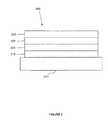
- FIG. 1shows an organic light emitting device 100 .
- Device 100may include a substrate 110 , an anode 115 , a hole injection layer 120 , a hole transport layer 125 , an electron blocking layer 130 , an emissive layer 135 , a hole blocking layer 140 , an electron transport layer 145 , an electron injection layer 150 , a protective layer 155 , and a cathode 160 .
- Cathode 160is a compound cathode having a first conductive layer 162 and a second conductive layer 164 .
- Device 100may be fabricated by depositing the layers described, in order. The properties and functions of these various layers, as well as example materials, are described in more detail in U.S. Pat. No. 7,279,704 at cols. 6-10, which are incorporated by reference.
- each of these layersare available.
- a flexible and transparent substrate-anode combinationis disclosed in U.S. Pat. No. 5,844,363, which is incorporated by reference in its entirety.
- An example of a p-doped hole transport layeris m-MTDATA doped with F.sub.4-TCNQ at a molar ratio of 50:1, as disclosed in U.S. Patent Application Publication No. 2003/0230980, which is incorporated by reference in its entirety.
- Examples of emissive and host materialsare disclosed in U.S. Pat. No. 6,303,238 to Thompson et al., which is incorporated by reference in its entirety.
- An example of an n-doped electron transport layeris BPhen doped with Li at a molar ratio of 1:1, as disclosed in U.S. Patent Application Publication No. 2003/0230980, which is incorporated by reference in its entirety.
- the theory and use of blocking layersis described in more detail in U.S. Pat. No. 6,097,147 and U.S. Patent Application Publication No.
- FIG. 2shows an inverted OLED 200 .
- the deviceincludes a substrate 210 , a cathode 215 , an emissive layer 220 , a hole transport layer 225 , and an anode 230 .
- Device 200may be fabricated by depositing the layers described, in order. Because the most common OLED configuration has a cathode disposed over the anode, and device 200 has cathode 215 disposed under anode 230 , device 200 may be referred to as an “inverted” OLED. Materials similar to those described with respect to device 100 may be used in the corresponding layers of device 200 .
- FIG. 2provides one example of how some layers may be omitted from the structure of device 100 .
- FIGS. 1 and 2The simple layered structure illustrated in FIGS. 1 and 2 is provided by way of non-limiting example, and it is understood that embodiments of the invention may be used in connection with a wide variety of other structures.
- the specific materials and structures describedare exemplary in nature, and other materials and structures may be used.
- Functional OLEDsmay be achieved by combining the various layers described in different ways, or layers may be omitted entirely, based on design, performance, and cost factors. Other layers not specifically described may also be included. Materials other than those specifically described may be used. Although many of the examples provided herein describe various layers as comprising a single material, it is understood that combinations of materials, such as a mixture of host and dopant, or more generally a mixture, may be used. Also, the layers may have various sublayers.
- hole transport layer 225transports holes and injects holes into emissive layer 220 , and may be described as a hole transport layer or a hole injection layer.
- an OLEDmay be described as having an “organic layer” disposed between a cathode and an anode. This organic layer may comprise a single layer, or may further comprise multiple layers of different organic materials as described, for example, with respect to FIGS. 1 and 2 .
- OLEDscomprised of polymeric materials (PLEDs) such as disclosed in U.S. Pat. No. 5,247,190 to Friend et al., which is incorporated by reference in its entirety.
- PLEDspolymeric materials
- OLEDs having a single organic layermay be used.
- OLEDsmay be stacked, for example as described in U.S. Pat. No. 5,707,745 to Forrest et al, which is incorporated by reference in its entirety.
- the OLED structuremay deviate from the simple layered structure illustrated in FIGS. 1 and 2 .
- the substratemay include an angled reflective surface to improve out-coupling, such as a mesa structure as described in U.S. Pat. No. 6,091,195 to Forrest et al., and/or a pit structure as described in U.S. Pat. No. 5,834,893 to Bulovic et al., which are incorporated by reference in their entireties.
- any of the layers of the various embodimentsmay be deposited by any suitable method.
- preferred methodsinclude thermal evaporation, ink-jet, such as described in U.S. Pat. Nos. 6,013,982 and 6,087,196, which are incorporated by reference in their entireties, organic vapor phase deposition (OVPD), such as described in U.S. Pat. No. 6,337,102 to Forrest et al., which is incorporated by reference in its entirety, and deposition by organic vapor jet printing (OVJP), such as described in U.S. patent application Ser. No. 10/233,470, which is incorporated by reference in its entirety.
- OVPDorganic vapor phase deposition
- OJPorganic vapor jet printing
- Other suitable deposition methodsinclude spin coating and other solution based processes.
- Solution based processesare preferably carried out in nitrogen or an inert atmosphere.
- preferred methodsinclude thermal evaporation.
- Preferred patterning methodsinclude deposition through a mask, cold welding such as described in U.S. Pat. Nos. 6,294,398 and 6,468,819, which are incorporated by reference in their entireties, and patterning associated with some of the deposition methods such as ink-jet and OVJD. Other methods may also be used.
- the materials to be depositedmay be modified to make them compatible with a particular deposition method. For example, substituents such as alkyl and aryl groups, branched or unbranched, and preferably containing at least 3 carbons, may be used in small molecules to enhance their ability to undergo solution processing.
- Substituents having 20 carbons or moremay be used, and 3-20 carbons is a preferred range. Materials with asymmetric structures may have better solution processibility than those having symmetric structures, because asymmetric materials may have a lower tendency to recrystallize. Dendrimer substituents may be used to enhance the ability of small molecules to undergo solution processing.
- Devices fabricated in accordance with embodiments of the inventionmay be incorporated into a wide variety of consumer products, including flat panel displays, computer monitors, televisions, billboards, lights for interior or exterior illumination and/or signaling, heads up displays, fully transparent displays, flexible displays, laser printers, telephones, cell phones, personal digital assistants (PDAs), laptop computers, digital cameras, camcorders, viewfinders, micro-displays, vehicles, a large area wall, theater or stadium screen, or a sign.
- PDAspersonal digital assistants
- Various control mechanismsmay be used to control devices fabricated in accordance with the present invention, including passive matrix and active matrix. Many of the devices are intended for use in a temperature range comfortable to humans, such as 18 degrees C. to 30 degrees C., and more preferably at room temperature (20-25 degrees C.).
- the materials and structures described hereinmay have applications in devices other than OLEDs.
- other optoelectronic devicessuch as organic solar cells and organic photodetectors may employ the materials and structures.
- organic devicessuch as organic transistors, may employ the materials and structures.
- An method of fabricating an organic light emitting deviceis provided.
- a first electrodeis provided, over which the rest of the device will be fabricated.
- a first organic layeris deposited over the first electrode via solution processing.
- the first organic layerincludes:
- FIG. 3shows an example of device 300 fabricated using the described method.
- the deviceis fabricated on a substrate 310 .
- the deviceincludes a first electrode 320 , emitting layers 330 disposed over the first electrode 320 , and a second electrode 340 disposed over the emitting layers 330 .
- Emitting layers 330include first organic layer 332 and second organic layer 334 .
- First electrode 320is preferably an anode and second electrode 340 is preferably a cathode, but other configurations may be used.
- First electrode 320may be provided by any suitable method, including the purchase of commercially available substrates pre-coated with indium tin oxide (ITO) or other electrode material.
- First organic layer 332is deposited via solution deposition over first electrode 320 .
- the solution used to deposit first organic layer 332includes a solvent, the organic host material of the first organic layer; the first organic emitting material of the first organic layer; and the second organic emitting material of the first organic layer. Other materials may be included.
- Second organic layer 334is deposited over and in direct contact with first organic layer 332 .
- Second organic layer 334includes an organic emitting material of the second organic layer.
- Second electrode 340is subsequently deposited over second organic layer 334 by any suitable technique.
- Device 300 as illustratedalso includes optional layers.
- a third organic layer 350 and a fourth organic layer 360are disposed between emitting layers 330 and first electrode 320 . Where first electrode 320 is an anode, third organic layer 350 may be a hole injection layer and fourth organic layer may be a hole transport layer.
- a fifth organic layer 370is disposed between emitting layers 330 and second electrode 340 . Where second electrode 340 is a cathode, fourth organic layer 370 may include a hole blocking layer, and an electron transport layer.
- Third, fourth and fifth organic layers 350 , 360 and 370may include sublayers, and may include other layers useful in various OLED architectures, many of which are described with respect to FIGS. 1 and 2 .
- the first organic emitting material of first organic layer 332has a peak emissive wavelength in the visible spectrum of 590-700 nm
- the second organic emitting material of first organic layer 332has a peak emissive wavelength in the visible spectrum at 500-590 nm
- the organic emitting material of second organic layer 334has a peak emissive wavelength in the visible spectrum of 400-500 nm.
- peak wavelengthscorrespond roughly to red, green, and blue emitters, and are useful for obtaining a device that emits white light that would be useful, for example, for general illumination purposes.
- the first organic emitting material of first organic layer 332is present in first organic layer 332 in a concentration of 0.01-5 wt %
- the second organic emitting material of first organic layer 332is present in the first organic layer in a concentration that is 1.1 to 500 times the concentration of the concentration of the first organic emitting material.
- the second organic emitting material of first organic layer 332is present in an amount not more than 40 wt %. Percentages are given as weight percentages of the organic layer after fabrication, and may generally be determined by using the relative weight percentages in solution of the various materials to be deposited, because the solvent evaporates.
- the first organic emitting material of first organic layer 332is present in the in first organic layer 332 in a concentration of 0.2-4 wt %
- the second organic emitting material of first organic layer 332is present in first organic layer 332 in a concentration that is 2 to 200 times the concentration of the concentration of the first organic emitting material.
- the second organic emitting material of first organic layer 332is preferably present in an amount not more than 40 wt %.
- the first organic emitting material of first organic layer 332 , the second organic emitting material of first organic layer 332 , and the organic emitting material of second organic layer 334are all small molecule materials.
- Many small molecule materialsare suitable for solution deposition, or may be readily modified to render them suitable for solution deposition using known techniques involving the addition of bulky substituents.
- second organic layer 334comprises an organic host and the organic emitting material of second organic layer 334 .
- second organic 334 layeris deposited by vapor deposition, where the organic host of second organic layer 334 and the organic emitting material of second organic layer 334 are co-deposited.
- Vapor depositionincludes vapor thermal evaporation (VTE), organic vapor phase deposition (OVPD), and organic vapor jet printing (OVJP). Vapor deposition is preferred because treatments to render underlying layers (such as first organic layer 332 ) insolvent often involve steps that would be detrimental to emitting materials. However, where techniques exist for solution depositing one emissive layer over another, those techniques may be used to deposit second organic layer 334 over first organic layer 332 .
- Third and fourth organic layers 350 and 360when present, are preferably deposited via solution deposition techniques. Because these organic layers do not include emitting materials, material and processing choices are readily available that render these layers insoluble in a solvent used to deposit subsequent layers. One such process choice is baking to cross-link the material, rendering it insoluble.
- the organic light emitting deviceemits light having a CIE coordinate of x coordinate in the range of 0.15-0.65, and y coordinate in the range of 0.1-0.7. More preferably, the organic light emitting device emits light having a CIE coordinate of x coordinate in the range of 0.25-0.5, and y coordinate in the range of 0.2-0.5. These CIE coordinates are readily obtainable using the preferred peak wavelength choices for the emitting materials of the device.
- first organic layer 332includes a small amount of red dopant, and a larger amount of green dopant.
- the amount of red dopantwill generally be small, both in absolute terms and relative to the amount of green dopant. This is because when a red dopant is co-doped with a green dopant, excitons may preferentially move to the red dopant or transfer from the green dopant to the red dopant due to the lower energy of the red dopant.
- red dopantDue to this preferential emission from the red dopant, a significantly smaller amount of red and larger amount of green is needed than if the materials were in separate layers.
- amount of emission from red dopant relative to green dopantis highly sensitive to small variations in the concentrations of the dopants, again due to the preferential emission from the red dopant.
- Controlling the amount of dopant deposited via vapor deposition techniques such as VTEgenerally involves adjusting temperatures, aperture sizes and relative flow rates of materials.
- the variance in the amount of dopant deposited from run to runis typically about 5%. So if it were desired to deposit a layer having 1 wt % of red dopant, the actual amount of red dopant would be about 0.95 wt % to 1.05 wt %. Where the device includes a layer having co-doped red and green dopants (and the green dopant will also be expected to have a 5% variance), the variance is large enough to significantly alter the CIE coordinates of a device.
- controlling the amount of dopant for solution process techniquesgenerally involves weighing the various materials and adding them to a solvent in carefully controlled amounts.
- a weight as low as 0.001 g of red dopantcan be measured for use in solution using a micro balance with a precision of 0.00001 g (plus or minus).
- varianceis 1%. This reduction in variance is expected to significantly improve the reproducibility of the CIE coordinates of the finished device.
- concentrations for a layer including only red and green dopantsare about 1 wt % for the red dopant and about 12 wt % for the green dopant. Other combinations of dopants, and other concentrations may be used.
- a solution processed emitting layermay include three or more emitting materials.
- An example of this useful for a white-emitting deviceis a layer that includes 72 wt % host, 20 wt % green emitter, 5 wt % yellow and 3 wt % red.
- Another exampleis 68.9 wt % host, 30 wt % green, 1% red1, and 0.1% red2 where red1 and red2 are different red emitting materials.
- the first organic layermay further comprises a third organic emitting material of the first organic layer.
- a third organic dopantmay be useful, for example, to add an additional emission color to fine tune the overall emission of the device, to adjust conductivity, or other uses.
- Emissive “dopants”may include phosphorescent emitting organic materials or fluorescent organic emitting materials.
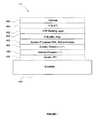
- Device 400is a preferred specific structure of device 300 .
- Device 400is fabricated on a substrate 410 , and includes, in order, anode 420 , solution processed organic hole injection layer 452 , solution processed organic hole transport layer 454 , solution processed organic emissive layer 432 , VTE deposited organic emissive layer 434 , VTE deposited organic blocking layer 462 , VTE deposited organic electron transport layer 464 and cathode 440 .
- Solution processed organic emissive layer 432includes a host and red and green emitting dopants
- VTE deposited organic emissive layer 434includes a host and a blue emitting dopant.
- FIG. 5shows a comparative example that does not include a solution deposited layer having multiple emissive dopants.
- Device 500is fabricated on a substrate 510 , and includes, in order, anode 520 , VTE deposited organic hole injection layer 552 , VTE deposited organic hole transport layer 554 , VTE deposited organic emissive layer 532 , VTE deposited organic emissive layer 534 , VTE deposited organic blocking layer 562 , VTE deposited organic electron transport layer 464 and cathode 440 .
- VTE deposited organic emissive layer 532includes a host and red and green emitting dopants
- VTE deposited organic emissive layer 534includes a host and a blue emitting dopant.
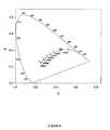
- FIG. 6shows a CIE diagram.
- the staris located at a target CIE coordinate that is desirable for white emission.
- the curve on which the star is locatedis the well-known black-body radiation curve, which describes the color of thermal radiation from an object that absorbs all electromagnetic radiation that falls on it (a “black body”).
- FIG. 7shows a target spectrum calculated using the emission spectra of the red, green and blue emitting materials of Example 1.
- LG101 and LG201available for purchase from LG Chemical Corporation of Seoul, Korea.
- NS60available for purchase from Nippon Steel Chemical Company of Tokyo, Japan.
- the color difference between different devicescan be described by MacAdam Ellipses, which are a well-known measure of human ability to differentiate color.
- a MacAdam Ellipseis a region on a CIE diagram inside of which a particular number of humans can not differentiate between colors.
- 68% of peoplecan perceive a color difference. 68% is the percentage that falls within one standard deviation on a bell curve.
- 95% of peoplecan perceive a color difference, where 95% is the percentage that falls within two standard deviations on a bell curve, and so on.
- the lighting industrygenerally desires that the color of a light used for illumination be reproducible within a 3- or 4-step MacAdam ellipse. If color reproducibility is too low, a viewer looking at two sources of illumination would perceive significant differences. For example, the different panels of a ceiling light might appear to have different colors, or there might be a significantly perceivable variation within a panel, which is undesirable.
- FIG. 8shows the CIE coordinates of the seven devices having the structure shown in FIG. 5 .
- FIG. 9shows the same data as FIG. 8 , but the relevant region of the diagram is magnified.
- FIG. 10shows the measured spectra for the seven devices. It can be seen that there is a significant spread in the CIE coordinates of the different devices, and that they are all well outside of a 3-step MacAdam ellipse centered around the average of the CIE coordinates (0.424, 0.413) of the seven devices.
- the 7-step MacAdam ellipsecan barely enclose the 7 device colors, which is out of industrial standard tolerance specification. This means that color reproducibility is not reliable for the VTE devices notwithstanding the care taken to achieve color reproducibility.
- the inventorsattribute this variation in color to the sensitivity of the co-doped green and red emitting layer to the percentage of red dopant, and the relatively high variation in this percentage that occurs with a VTE deposition process.
- a devicewas fabricated having the structure shown in FIG. 4 .
- the hole injecting material HIL-1 (as the host material) along with Conducting dopant-1were dissolved in a cyclohexanone solution.
- the amount of Conducting dopant-1 in the solutionwas 10 wt % relative to the host material HIL-1.
- the total concentration of the HIL-1 and Conducting dopant-1was 0.5 wt % in cyclohexanone.
- HILhole injection layer
- the solutionwas spin-coated at 4000 rpm for 60 seconds onto a patterned indium tin oxide (ITO) electrode.
- ITOindium tin oxide
- the resulting filmwas baked for 30 minutes at 250° C. The film became insoluble after baking.
- HTLhole transporting layer
- EMLemitting layer
- the red and green EMLwas composed of a host material (Host-1) and a red and a green phosphorescent dopant (Red dopant-1 and Green dopant-1) as the emitting material.
- a toluene solution containing Host-1, Green dopant-1, and Red dopant (of total 0.75 wt %) with a Host-1:Green dopant-11:Red dopant-1 weight ratio of 87:12:1was spin-coated onto the insoluble HTL at 1000 rpm for 60 seconds, and then baked at 100° C. for 60 minutes.
- the blue EMLwas deposited using thermal evaporation.
- the 10 nm of blue host (Host-2) and Blue dopant-1was co-evaporated with ratio of 90:10.
- On top of blue EML5 nm neat Host-2 was evaporated to build blocking layer (BL).
- the electron transport layer (containing Alq3), the electron injection layer (containing LiF), and the aluminum electrodewere sequentially vacuum deposited.
- ITO120 nm
- HIL-1Conducting Dopant-1 (90:10; 5 nm)/HTL-1 (10 nm)/Host-1:Green Dopant-1:Red Dopant-1 (87:12:1; 25 nm)/Host-2:Blue Dopant-1: (90:10; 10 nm)/Host-2 (5 nm)/Alq (40 nm)/LiF/Al
- the CIE coordinate and spectrum of the hybrid white device of Example 2are shown in FIGS. 6 and 7 , respectively.
- the device performanceis described in TABLE 1. At 1000 cd/m2, the power efficiency was 11 lm/W with color rendering index (CRI) 78, and correlated color temperature (CCT) corresponding to the white color was 2800K degree.
- CRIcolor rendering index
- CCTcorrelated color temperature
- Example 2Power Efficiency (lm/W) @ 1,000 cd/m2 11 Correlated Color Temperature (CCT) (K) @ 1,000 cd/m2 2800 Color Rendering Index (CRI) @ 1,000 cd/m2 78 Color Coordinate, CIE(x, y) @ 1,000 cd/m2 (0.453, 0.411) Lifetime LT80 (hours) @ 4,000 cd/m2 100 (A brightness decay to 80% of initial level 4,000 cd/m2)
Landscapes
- Engineering & Computer Science (AREA)
- Manufacturing & Machinery (AREA)
- Physics & Mathematics (AREA)
- Optics & Photonics (AREA)
- Electroluminescent Light Sources (AREA)
Abstract
Description
- i. an organic host material of the first organic layer;
- ii. a first organic emitting material of the first organic layer;
- iii. a second organic emitting material of the first organic layer;
A second organic layer is deposited over and in direct contact with the first organic layer. The second organic layer includes an organic emitting material of the second organic layer. A second electrode is then deposited over the second organic layer. The device may include other layers.
- depositing a third organic layer comprising an organic material of the third organic layer over the first electrode via solution processing; and
- depositing a fourth organic layer comprising an organic material of the fourth organic layer over the third organic layer via solution processing.
Preferably the third organic layer does not dissolve when the fourth organic layer is deposited, and the fourth organic layer does not dissolve when the first organic layer is deposited.
- i. an organic host material of the first organic layer;
- ii. a first organic emitting material of the first organic layer;
- iii. a second organic emitting material of the first organic layer.
A second organic layer is deposited over and in direct contact with the first organic layer. The second organic layer includes an organic emitting material of the second organic layer. A second electrode is then deposited over the second organic layer. The device may include other layers.


LG101 and LG201, available for purchase from LG Chemical Corporation of Seoul, Korea. NS60, available for purchase from Nippon Steel Chemical Company of Tokyo, Japan.
| TABLE 1 |
| Hybrid white device performances of Example 2 |
| Power Efficiency (lm/W) @ 1,000 cd/m2 | 11 |
| Correlated Color Temperature (CCT) (K) @ 1,000 cd/m2 | 2800 |
| Color Rendering Index (CRI) @ 1,000 cd/m2 | 78 |
| Color Coordinate, CIE(x, y) @ 1,000 cd/m2 | (0.453, 0.411) |
| Lifetime LT80 (hours) @ 4,000 cd/m2 | 100 |
| (A brightness decay to 80% of initial level 4,000 cd/m2) | |
Claims (13)
Priority Applications (1)
| Application Number | Priority Date | Filing Date | Title |
|---|---|---|---|
| US14/219,855US9054344B2 (en) | 2010-01-20 | 2014-03-19 | Electroluminescent devices for lighting applications |
Applications Claiming Priority (4)
| Application Number | Priority Date | Filing Date | Title |
|---|---|---|---|
| US29668010P | 2010-01-20 | 2010-01-20 | |
| US12/913,443US8288187B2 (en) | 2010-01-20 | 2010-10-27 | Electroluminescent devices for lighting applications |
| US13/614,026US20130002132A1 (en) | 2010-01-20 | 2012-09-13 | Electroluminescent devices for lighting applications |
| US14/219,855US9054344B2 (en) | 2010-01-20 | 2014-03-19 | Electroluminescent devices for lighting applications |
Related Parent Applications (1)
| Application Number | Title | Priority Date | Filing Date |
|---|---|---|---|
| US13/614,026ContinuationUS20130002132A1 (en) | 2010-01-20 | 2012-09-13 | Electroluminescent devices for lighting applications |
Publications (2)
| Publication Number | Publication Date |
|---|---|
| US20140206121A1 US20140206121A1 (en) | 2014-07-24 |
| US9054344B2true US9054344B2 (en) | 2015-06-09 |
Family
ID=44277870
Family Applications (3)
| Application Number | Title | Priority Date | Filing Date |
|---|---|---|---|
| US12/913,443ActiveUS8288187B2 (en) | 2010-01-20 | 2010-10-27 | Electroluminescent devices for lighting applications |
| US13/614,026AbandonedUS20130002132A1 (en) | 2010-01-20 | 2012-09-13 | Electroluminescent devices for lighting applications |
| US14/219,855ActiveUS9054344B2 (en) | 2010-01-20 | 2014-03-19 | Electroluminescent devices for lighting applications |
Family Applications Before (2)
| Application Number | Title | Priority Date | Filing Date |
|---|---|---|---|
| US12/913,443ActiveUS8288187B2 (en) | 2010-01-20 | 2010-10-27 | Electroluminescent devices for lighting applications |
| US13/614,026AbandonedUS20130002132A1 (en) | 2010-01-20 | 2012-09-13 | Electroluminescent devices for lighting applications |
Country Status (7)
| Country | Link |
|---|---|
| US (3) | US8288187B2 (en) |
| EP (1) | EP2526577B1 (en) |
| JP (3) | JP5642805B2 (en) |
| KR (2) | KR20170021376A (en) |
| CN (2) | CN102792480B (en) |
| TW (2) | TWI566452B (en) |
| WO (1) | WO2011090535A1 (en) |
Cited By (1)
| Publication number | Priority date | Publication date | Assignee | Title |
|---|---|---|---|---|
| US11081664B2 (en)* | 2016-12-27 | 2021-08-03 | Xianyang Chvt New Display Technology Co., Ltd. | Organic electroluminescent element having stacked light emitting units |
Families Citing this family (39)
| Publication number | Priority date | Publication date | Assignee | Title |
|---|---|---|---|---|
| US8288187B2 (en)* | 2010-01-20 | 2012-10-16 | Universal Display Corporation | Electroluminescent devices for lighting applications |
| TW201221597A (en)* | 2010-11-03 | 2012-06-01 | Cambrios Technologies Corp | Coating compositions for forming nanocomposite films |
| KR102012047B1 (en) | 2012-01-06 | 2019-08-19 | 유니버셜 디스플레이 코포레이션 | Highly efficient phosphorescent materials |
| US9190626B2 (en)* | 2012-05-31 | 2015-11-17 | Lg Chem, Ltd. | Organic light emitting diode having low driving voltage, high brightness, and excellent light emitting efficiencies |
| JP6333262B2 (en) | 2012-09-20 | 2018-05-30 | ユー・ディー・シー アイルランド リミテッド | Azadibenzofuran for electronic applications |
| GB2509718A (en)* | 2013-01-09 | 2014-07-16 | Cambridge Display Tech Ltd | Method for forming a layer of an electronic device and appropriate precursor compounds |
| US8809848B1 (en)* | 2013-03-07 | 2014-08-19 | National Tsing Hua University | Full-band and high-CRI organic light-emitting diode |
| US10074806B2 (en)* | 2013-08-20 | 2018-09-11 | Universal Display Corporation | Organic electroluminescent materials and devices |
| US9385348B2 (en)* | 2013-08-29 | 2016-07-05 | The Regents Of The University Of Michigan | Organic electronic devices with multiple solution-processed layers |
| CN105723536A (en) | 2013-08-29 | 2016-06-29 | 密执安州立大学董事会 | Organic electronic devices with multiple solution-processed layers |
| EP3063153B1 (en) | 2013-10-31 | 2018-03-07 | Idemitsu Kosan Co., Ltd. | Azadibenzothiophenes for electronic applications |
| WO2015163174A1 (en)* | 2014-04-25 | 2015-10-29 | 住友化学株式会社 | Light-emitting element |
| JP2014220248A (en)* | 2014-06-25 | 2014-11-20 | 三菱化学株式会社 | Method of manufacturing organic electroluminescent element |
| EP3174885B1 (en) | 2014-07-28 | 2019-10-02 | Idemitsu Kosan Co., Ltd. | 2,9-functionalized benzimidazolo[1,2-a]benzimidazoles as hosts for organic light emitting diodes (oleds) |
| EP2982676B1 (en) | 2014-08-07 | 2018-04-11 | Idemitsu Kosan Co., Ltd. | Benzimidazo[2,1-B]benzoxazoles for electronic applications |
| EP3466957A1 (en) | 2014-08-08 | 2019-04-10 | UDC Ireland Limited | Oled comprising an electroluminescent imidazo-quinoxaline carbene metal complexes |
| EP2993215B1 (en) | 2014-09-04 | 2019-06-19 | Idemitsu Kosan Co., Ltd. | Azabenzimidazo[2,1-a]benzimidazoles for electronic applications |
| EP3015469B1 (en) | 2014-10-30 | 2018-12-19 | Idemitsu Kosan Co., Ltd. | 5-(benzimidazol-2-yl)benzimidazo[1,2-a]benzimidazoles for electronic applications |
| WO2016079667A1 (en) | 2014-11-17 | 2016-05-26 | Idemitsu Kosan Co., Ltd. | Indole derivatives for electronic applications |
| KR102512938B1 (en) | 2014-11-18 | 2023-03-23 | 유디씨 아일랜드 리미티드 | Pt- or pd-carbene complexes for use in organic light emitting diodes |
| EP3034506A1 (en) | 2014-12-15 | 2016-06-22 | Idemitsu Kosan Co., Ltd | 4-functionalized carbazole derivatives for electronic applications |
| EP3034507A1 (en) | 2014-12-15 | 2016-06-22 | Idemitsu Kosan Co., Ltd | 1-functionalized dibenzofurans and dibenzothiophenes for organic light emitting diodes (OLEDs) |
| EP3235891B1 (en)* | 2015-02-03 | 2020-12-23 | Sumitomo Chemical Company, Ltd. | Composition and light-emitting element using same |
| EP3053918B1 (en) | 2015-02-06 | 2018-04-11 | Idemitsu Kosan Co., Ltd. | 2-carbazole substituted benzimidazoles for electronic applications |
| EP3054498B1 (en) | 2015-02-06 | 2017-09-20 | Idemitsu Kosan Co., Ltd. | Bisimidazodiazocines |
| EP3061759B1 (en) | 2015-02-24 | 2019-12-25 | Idemitsu Kosan Co., Ltd | Nitrile substituted dibenzofurans |
| EP3070144B1 (en) | 2015-03-17 | 2018-02-28 | Idemitsu Kosan Co., Ltd. | Seven-membered ring compounds |
| EP3072943B1 (en) | 2015-03-26 | 2018-05-02 | Idemitsu Kosan Co., Ltd. | Dibenzofuran/carbazole-substituted benzonitriles |
| EP3075737B1 (en) | 2015-03-31 | 2019-12-04 | Idemitsu Kosan Co., Ltd | Benzimidazolo[1,2-a]benzimidazole carrying aryl- or heteroarylnitril groups for organic light emitting diodes |
| WO2017056055A1 (en) | 2015-10-01 | 2017-04-06 | Idemitsu Kosan Co., Ltd. | Benzimidazolo[1,2-a]benzimidazole carrying triazine groups for organic light emitting diodes |
| EP3150604B1 (en) | 2015-10-01 | 2021-07-14 | Idemitsu Kosan Co., Ltd. | Benzimidazolo[1,2-a]benzimidazole carrying benzimidazolo[1,2-a]benzimidazolylyl groups, carbazolyl groups, benzofurane groups or benzothiophene groups for organic light emitting diodes |
| WO2017056053A1 (en) | 2015-10-01 | 2017-04-06 | Idemitsu Kosan Co., Ltd. | Benzimidazolo[1,2-a]benzimidazole carrying benzimidazolo[1,2-a]benzimidazolyl groups, carbazolyl groups, benzofurane groups or benzothiophene groups for organic light emitting diodes |
| EP3150606B1 (en) | 2015-10-01 | 2019-08-14 | Idemitsu Kosan Co., Ltd. | Benzimidazolo[1,2-a]benzimidazoles carrying benzofurane or benzothiophene groups for organic light emitting diodes |
| WO2017078182A1 (en) | 2015-11-04 | 2017-05-11 | Idemitsu Kosan Co., Ltd. | Benzimidazole fused heteroaryls |
| US11174258B2 (en) | 2015-12-04 | 2021-11-16 | Idemitsu Kosan Co., Ltd. | Benzimidazolo[1,2-a]benzimidazole derivatives for organic light emitting diodes |
| KR102684614B1 (en) | 2015-12-21 | 2024-07-15 | 유디씨 아일랜드 리미티드 | Transition metal complexes with tripodal ligands and the use thereof in oleds |
| KR102553276B1 (en)* | 2016-03-29 | 2023-07-06 | 엘지디스플레이 주식회사 | Organic light emitting display device |
| US10968229B2 (en) | 2016-04-12 | 2021-04-06 | Idemitsu Kosan Co., Ltd. | Seven-membered ring compounds |
| US10770673B2 (en)* | 2017-11-28 | 2020-09-08 | The Regents Of The University Of Michigan | Highly reliable stacked white organic light emitting device |
Citations (243)
| Publication number | Priority date | Publication date | Assignee | Title |
|---|---|---|---|---|
| US4769292A (en) | 1987-03-02 | 1988-09-06 | Eastman Kodak Company | Electroluminescent device with modified thin film luminescent zone |
| US5061569A (en) | 1990-07-26 | 1991-10-29 | Eastman Kodak Company | Electroluminescent device with organic electroluminescent medium |
| US5247190A (en) | 1989-04-20 | 1993-09-21 | Cambridge Research And Innovation Limited | Electroluminescent devices |
| US5427858A (en) | 1990-11-30 | 1995-06-27 | Idemitsu Kosan Company Limited | Organic electroluminescence device with a fluorine polymer layer |
| US5503910A (en) | 1994-03-29 | 1996-04-02 | Idemitsu Kosan Co., Ltd. | Organic electroluminescence device |
| US5518824A (en) | 1993-08-02 | 1996-05-21 | Basf Aktiengesellschaft | Electroluminescent arrangement |
| US5552253A (en) | 1995-03-31 | 1996-09-03 | Xerox Corporation | Multiple layer photoreceptor for color xerography |
| US5681756A (en) | 1994-05-31 | 1997-10-28 | Motorola | Method of fabricating an integrated multicolor organic led array |
| US5693428A (en) | 1995-02-06 | 1997-12-02 | Sanyo Electric Co., Ltd. | Organic electroluminescent device |
| US5703436A (en) | 1994-12-13 | 1997-12-30 | The Trustees Of Princeton University | Transparent contacts for organic devices |
| US5707745A (en) | 1994-12-13 | 1998-01-13 | The Trustees Of Princeton University | Multicolor organic light emitting devices |
| WO1998024271A1 (en) | 1996-11-25 | 1998-06-04 | Seiko Epson Corporation | Method of producing organic el elements, organic el elements and organic el display device |
| JPH10162955A (en) | 1996-11-28 | 1998-06-19 | Seiko Precision Kk | Manufacture of organic el element |
| EP0650955B1 (en) | 1993-11-01 | 1998-08-19 | Hodogaya Chemical Co., Ltd. | Amine compound and electro-luminescence device comprising same |
| US5834893A (en) | 1996-12-23 | 1998-11-10 | The Trustees Of Princeton University | High efficiency organic light emitting devices with light directing structures |
| US5837391A (en) | 1996-01-17 | 1998-11-17 | Nec Corporation | Organic electroluminescent element having electrode between two fluorescent media for injecting carrier thereinto |
| US5844363A (en) | 1997-01-23 | 1998-12-01 | The Trustees Of Princeton Univ. | Vacuum deposited, non-polymeric flexible organic light emitting devices |
| US5851709A (en) | 1997-10-31 | 1998-12-22 | Eastman Kodak Company | Method for selective transfer of a color organic layer |
| US5853905A (en) | 1997-09-08 | 1998-12-29 | Motorola, Inc. | Efficient single layer electroluminescent device |
| WO1999012396A1 (en) | 1997-09-01 | 1999-03-11 | Seiko Epson Corporation | Electroluminescent element and method of producing the same |
| WO1999021935A1 (en) | 1997-10-23 | 1999-05-06 | Isis Innovation Limited | Light-emitting dendrimers and devices |
| US5922481A (en) | 1995-01-13 | 1999-07-13 | Basf Aktiengesellschaft | Electroluminescent arrangement |
| US5929194A (en) | 1996-02-23 | 1999-07-27 | The Dow Chemical Company | Crosslinkable or chain extendable polyarylpolyamines and films thereof |
| US6013982A (en) | 1996-12-23 | 2000-01-11 | The Trustees Of Princeton University | Multicolor display devices |
| JP2000036386A (en) | 1998-07-16 | 2000-02-02 | Alps Electric Co Ltd | White light emitting electroluminescence element |
| US6066357A (en) | 1998-12-21 | 2000-05-23 | Eastman Kodak Company | Methods of making a full-color organic light-emitting display |
| US6087196A (en) | 1998-01-30 | 2000-07-11 | The Trustees Of Princeton University | Fabrication of organic semiconductor devices using ink jet printing |
| US6091195A (en) | 1997-02-03 | 2000-07-18 | The Trustees Of Princeton University | Displays having mesa pixel configuration |
| JP2000208254A (en) | 1999-01-11 | 2000-07-28 | Seiko Epson Corp | Method for manufacturing organic EL element and organic EL display device |
| US6097147A (en) | 1998-09-14 | 2000-08-01 | The Trustees Of Princeton University | Structure for high efficiency electroluminescent device |
| US6107452A (en) | 1998-10-09 | 2000-08-22 | International Business Machines Corporation | Thermally and/or photochemically crosslinked electroactive polymers in the manufacture of opto-electronic devices |
| EP1030383A2 (en) | 1999-02-16 | 2000-08-23 | Sharp Kabushiki Kaisha | Charge-transport structures |
| US6130001A (en) | 1997-07-15 | 2000-10-10 | Motorola, Inc. | Organic electroluminescent device with continuous organic medium |
| US6221438B1 (en) | 1998-11-03 | 2001-04-24 | Sarnoff Corporation | Patterned deposition of a material |
| US6228436B1 (en) | 1998-12-16 | 2001-05-08 | Battelle Memorial Institute | Method of making light emitting polymer composite material |
| US20010003602A1 (en) | 1999-12-09 | 2001-06-14 | Yoshimasa Fujita | Coating liquid for forming organic led layer and method of manufacturing organic led device using it |
| US20010004469A1 (en) | 1997-10-15 | 2001-06-21 | Yoshio Himeshima | Process for manufacturing organic electroluminescent device |
| US20010015432A1 (en) | 2000-02-10 | 2001-08-23 | Tatsuya Igarashi | Light emitting device material comprising iridium complex and light emitting device using same material |
| US6294398B1 (en) | 1999-11-23 | 2001-09-25 | The Trustees Of Princeton University | Method for patterning devices |
| US6303238B1 (en) | 1997-12-01 | 2001-10-16 | The Trustees Of Princeton University | OLEDs doped with phosphorescent compounds |
| WO2001039234A3 (en) | 1999-11-24 | 2001-11-08 | Univ Princeton | Organic light emitting diode having a blue phosphorescent molecule as an emitter |
| US6337102B1 (en)* | 1997-11-17 | 2002-01-08 | The Trustees Of Princeton University | Low pressure vapor phase deposition of organic thin films |
| WO2002015645A1 (en) | 2000-08-11 | 2002-02-21 | The Trustees Of Princeton University | Organometallic compounds and emission-shifting organic electrophosphorescence |
| US20020034656A1 (en) | 1998-09-14 | 2002-03-21 | Thompson Mark E. | Organometallic complexes as phosphorescent emitters in organic LEDs |
| US6372154B1 (en) | 1999-12-30 | 2002-04-16 | Canon Kabushiki Kaisha | Luminescent ink for printing of organic luminescent devices |
| JP2002158091A (en) | 2000-11-16 | 2002-05-31 | Fuji Photo Film Co Ltd | Light-emitting element |
| US20020067123A1 (en) | 2000-03-31 | 2002-06-06 | Seiko Epson Corporation | Organic EL device and production method thereof |
| US20020074935A1 (en) | 2000-12-15 | 2002-06-20 | Kwong Raymond C. | Highly stable and efficient OLEDs with a phosphorescent-doped mixed layer architecture |
| JP2002175887A (en) | 2000-12-07 | 2002-06-21 | Denso Corp | Organic el element |
| US20020093283A1 (en) | 2001-01-17 | 2002-07-18 | Satoshi Seo | Luminescent device and method of manufacturing same |
| US6447934B1 (en) | 1998-10-09 | 2002-09-10 | Denso Corporation | Organic electroluminescent panel |
| US20020134984A1 (en) | 2001-02-01 | 2002-09-26 | Fuji Photo Film Co., Ltd. | Transition metal complex and light-emitting device |
| WO2002002714A3 (en) | 2000-06-30 | 2002-10-24 | Du Pont | Electroluminescent iridium compounds with fluorinated phenylpyridines, phenylpyrimidines, and phenylquinolines and devices made with such compounds |
| US20020158242A1 (en) | 1999-12-31 | 2002-10-31 | Se-Hwan Son | Electronic device comprising organic compound having p-type semiconducting characteristics |
| US6528187B1 (en) | 1998-09-08 | 2003-03-04 | Fuji Photo Film Co., Ltd. | Material for luminescence element and luminescence element using the same |
| US20030068525A1 (en) | 2001-08-16 | 2003-04-10 | 3M Innovative Properties Company | Method and materials for patterning of an amorphous, non-polymeric, organic matrix with electrically active material disposed therein |
| US20030072964A1 (en) | 2001-10-17 | 2003-04-17 | Kwong Raymond C. | Phosphorescent compounds and devices comprising the same |
| WO2003040257A1 (en) | 2001-11-07 | 2003-05-15 | E. I. Du Pont De Nemours And Company | Electroluminescent platinum compounds and devices made with such compounds |
| US6592969B1 (en) | 1998-04-02 | 2003-07-15 | Cambridge Display Technology Limited | Flexible substrates for organic devices |
| US20030138657A1 (en) | 2000-12-07 | 2003-07-24 | Canon Kabushiki Kaisha | Deuterated semi-conducting organic compounds used for opto-electronic devices |
| US20030152802A1 (en) | 2001-06-19 | 2003-08-14 | Akira Tsuboyama | Metal coordination compound and organic liminescence device |
| JP2003229272A (en) | 2002-01-31 | 2003-08-15 | Toyota Industries Corp | Organic el element |
| US20030162053A1 (en) | 1996-06-25 | 2003-08-28 | Marks Tobin J. | Organic light - emitting diodes and methods for assembly and enhanced charge injection |
| US20030175553A1 (en) | 2001-12-28 | 2003-09-18 | Thompson Mark E. | White light emitting oleds from combined monomer and aggregate emission |
| WO2003060956A3 (en) | 2002-01-18 | 2003-11-13 | Lg Chemical Ltd | New material for transporting electrons and organic electroluminescent display using the same |
| US20030230747A1 (en) | 2002-06-14 | 2003-12-18 | Nokia Corporation | Pre-patterned substrate for organic thin film transistor structures and circuits and related method for making same |
| US20030230980A1 (en) | 2002-06-18 | 2003-12-18 | Forrest Stephen R | Very low voltage, high efficiency phosphorescent oled in a p-i-n structure |
| US6687266B1 (en) | 2002-11-08 | 2004-02-03 | Universal Display Corporation | Organic light emitting materials and devices |
| US20040036077A1 (en) | 2002-08-22 | 2004-02-26 | Fuji Photo Film Co., Ltd. | Light emitting element |
| US20040037949A1 (en) | 2000-06-01 | 2004-02-26 | Wright Jeffrey Peter | Method of creating a color optoelectronic device |
| US20040048101A1 (en) | 2002-03-29 | 2004-03-11 | Thompson Mark E. | Organic light emitting devices with electron blocking layers |
| US20040095064A1 (en) | 2002-11-15 | 2004-05-20 | Lu Min-Hao Michael | Structure and method of fabricating organic devices |
| US20040094768A1 (en) | 2002-09-06 | 2004-05-20 | Gang Yu | Methods for producing full-color organic electroluminescent devices |
| US20040096570A1 (en) | 2002-11-15 | 2004-05-20 | Michael Weaver | Structure and method of fabricating organic devices |
| US20040115476A1 (en) | 2002-11-26 | 2004-06-17 | Tomohiro Oshiyama | Organic electroluminescent element, and display and illuminator |
| US20040137267A1 (en) | 2002-12-27 | 2004-07-15 | Fuji Photo Film Co., Ltd. | Organic electroluminescent device |
| US20040137268A1 (en) | 2002-12-27 | 2004-07-15 | Fuji Photo Film Co., Ltd. | Organic electroluminescent device |
| US20040174116A1 (en) | 2001-08-20 | 2004-09-09 | Lu Min-Hao Michael | Transparent electrodes |
| US20040189189A1 (en) | 1999-02-12 | 2004-09-30 | Cambridge Display Technology Ltd. | Opto-electrical devices |
| WO2004107822A1 (en) | 2003-05-29 | 2004-12-09 | Nippon Steel Chemical Co., Ltd. | Organic electroluminescent element |
| WO2004111066A1 (en) | 2003-06-09 | 2004-12-23 | Hitachi Chemical Co., Ltd. | Metal coordination compound, polymer composition, and organic electroluminescence element using them |
| JP2005011610A (en) | 2003-06-18 | 2005-01-13 | Nippon Steel Chem Co Ltd | Organic electroluminescence device |
| US20050025993A1 (en) | 2003-07-25 | 2005-02-03 | Thompson Mark E. | Materials and structures for enhancing the performance of organic light emitting devices |
| JP2005038672A (en) | 2003-07-18 | 2005-02-10 | Konica Minolta Holdings Inc | Organic electroluminescent element, lighting device, and display device |
| WO2005014551A1 (en) | 2003-08-07 | 2005-02-17 | Nippon Steel Chemical Co., Ltd. | Aluminum chelate compelx for organic el material |
| US20050046337A1 (en) | 2003-09-03 | 2005-03-03 | Byung-Doo Chin | Organic lights-emitting device with doped emission layer |
| US6869695B2 (en) | 2001-12-28 | 2005-03-22 | The Trustees Of Princeton University | White light emitting OLEDs from combined monomer and aggregate emission |
| US20050074630A1 (en) | 2003-03-27 | 2005-04-07 | Hiroshi Kanno | Organic electroluminescent device |
| WO2005030900A1 (en) | 2003-09-25 | 2005-04-07 | Nippon Steel Chemical Co., Ltd. | Organic electroluminescent device |
| US20050077817A1 (en) | 2002-12-26 | 2005-04-14 | Semiconductor Energy Laboratory Co., Ltd. | Organic light emitting element and a light emitting device using the same |
| EP0954205B1 (en) | 1998-03-24 | 2005-05-11 | Sony Corporation | Organic electroluminescent device and method for producing it |
| WO2005019373A3 (en) | 2003-08-19 | 2005-05-19 | Basf Ag | Transition metal complexes comprising carbene ligands serving as emitters for organic light-emitting diodes (oled's) |
| US20050112407A1 (en) | 2003-11-21 | 2005-05-26 | Fuji Photo Film Co., Ltd. | Organic electroluminescent device |
| US20050123751A1 (en) | 2003-08-25 | 2005-06-09 | Tetsuo Tsutsui | Electrode device for organic device, electronic device having electrode device for organic device, and method of forming electrode device for organic device |
| WO2004093207A3 (en) | 2003-04-15 | 2005-06-09 | Covion Organic Semiconductors | Mixtures of matrix materials and organic semiconductors capable of emission, use of the same and electronic components containing said mixtures |
| EP1238981B1 (en) | 2001-03-08 | 2005-06-15 | Canon Kabushiki Kaisha | Metal coordination compound, luminescence device and display apparatus |
| WO2005089025A1 (en) | 2004-03-15 | 2005-09-22 | Nippon Steel Chemical Co., Ltd. | Organic electroluminescent device |
| US20050238919A1 (en) | 2004-04-23 | 2005-10-27 | Fuji Photo Film Co., Ltd. | Organic electroluminescent device |
| US20050244673A1 (en) | 2002-08-27 | 2005-11-03 | Fujitsu Limited | Organometallic complex, organic EL element and organic EL display |
| US20050260441A1 (en) | 2004-05-18 | 2005-11-24 | Thompson Mark E | Luminescent compounds with carbene ligands |
| US20050260449A1 (en) | 2004-05-18 | 2005-11-24 | Robert Walters | Complexes with tridentate ligands |
| WO2005123873A1 (en) | 2004-06-17 | 2005-12-29 | Konica Minolta Holdings, Inc. | Organic electroluminescent device material, organic electroluminescent device, display and illuminating device |
| US6982179B2 (en) | 2002-11-15 | 2006-01-03 | University Display Corporation | Structure and method of fabricating organic devices |
| US20060008670A1 (en) | 2004-07-06 | 2006-01-12 | Chun Lin | Organic light emitting materials and devices |
| WO2006009024A1 (en) | 2004-07-23 | 2006-01-26 | Konica Minolta Holdings, Inc. | Organic electroluminescent device, display and illuminating device |
| US20060046098A1 (en) | 2000-03-27 | 2006-03-02 | Idemitsu Kosan Co., Ltd. | Organic electroluminescence element |
| US7009338B2 (en) | 2001-05-16 | 2006-03-07 | The University Of Southern California | High efficiency multi-color electro-phosphorescent OLEDs |
| US7022421B2 (en) | 2001-08-29 | 2006-04-04 | The University Of Southern California | Organic light emitting devices having carrier blocking layers comprising metal complexes |
| EP0982974B1 (en) | 1997-09-02 | 2006-05-03 | Seiko Epson Corporation | Organic el element manufacturing process |
| US20060121308A1 (en) | 2003-04-23 | 2006-06-08 | Eisaku Katoh | Material for organic electroluminescent device, organic electroluminescent device, illuminating device and display |
| EP1670082A2 (en) | 2004-12-13 | 2006-06-14 | Kabushiki Kaisha Toyota Jidoshokki | Organic el devices |
| US20060127696A1 (en) | 2002-08-24 | 2006-06-15 | Covion Organic Semiconductors Gmbh | Rhodium and iridium complexes |
| US20060141288A1 (en) | 2001-05-24 | 2006-06-29 | Idemitsu Kosan Co., Ltd. | Organic electroluminescence element |
| US7078113B2 (en) | 2001-08-29 | 2006-07-18 | The University Of Southern California | Organic light emitting devices having carrier transporting layers comprising metal complexes |
| US7087321B2 (en) | 2003-04-22 | 2006-08-08 | Universal Display Corporation | Organic light emitting devices having reduced pixel shrinkage |
| WO2006082742A1 (en) | 2005-02-04 | 2006-08-10 | Konica Minolta Holdings, Inc. | Organic electroluminescent device material, organic electroluminescent device, display and illuminating device |
| US7090928B2 (en) | 2003-04-01 | 2006-08-15 | The University Of Southern California | Binuclear compounds |
| US20060182992A1 (en) | 2003-06-02 | 2006-08-17 | Kazumi Nii | Organic electroluminescent devices and metal complex compounds |
| EP1701394A1 (en) | 2005-03-05 | 2006-09-13 | Samsung SDI Co., Ltd. | Organic electroluminescent device and method of manufacturing the same |
| US20060202194A1 (en) | 2005-03-08 | 2006-09-14 | Jeong Hyun C | Red phosphorescene compounds and organic electroluminescence device using the same |
| WO2006098120A1 (en) | 2005-03-16 | 2006-09-21 | Konica Minolta Holdings, Inc. | Organic electroluminescent device material and organic electroluminescent device |
| WO2006100298A1 (en) | 2005-03-24 | 2006-09-28 | Basf Aktiengesellschaft | Use of compounds containing aromatic or heteroaromatic rings linked via carbonyl group-containing groups, for use as matrix materials in organic light-emitting diodes |
| WO2006103874A1 (en) | 2005-03-29 | 2006-10-05 | Konica Minolta Holdings, Inc. | Organic electroluminescent device material, organic electroluminescent device, display and illuminating device |
| US20060232194A1 (en) | 2005-04-13 | 2006-10-19 | Yeh-Jiun Tung | Hybrid OLED having phosphorescent and fluorescent emitters |
| US20060240279A1 (en) | 2005-04-21 | 2006-10-26 | Vadim Adamovich | Non-blocked phosphorescent OLEDs |
| WO2006114966A1 (en) | 2005-04-18 | 2006-11-02 | Konica Minolta Holdings, Inc. | Organic electroluminescent device, display and illuminating device |
| US20060251923A1 (en) | 2005-05-06 | 2006-11-09 | Chun Lin | Stability OLED materials and devices |
| US20060263635A1 (en) | 2005-05-06 | 2006-11-23 | Fuji Photo Film Co., Ltd. | Organic electroluminescent device |
| WO2006132173A1 (en) | 2005-06-07 | 2006-12-14 | Nippon Steel Chemical Co., Ltd. | Organic metal complex and organic electroluminescent device using same |
| US20060280965A1 (en) | 2005-05-31 | 2006-12-14 | Raymond Kwong | Triphenylene hosts in phosphorescent light emitting diodes |
| US20060279203A1 (en)* | 2005-06-01 | 2006-12-14 | Stephen Forrest | Fluorescent filtered electrophosphorescence |
| US7151339B2 (en) | 2004-01-30 | 2006-12-19 | Universal Display Corporation | OLED efficiency by utilization of different doping concentrations within the device emissive layer |
| US7154114B2 (en) | 2004-05-18 | 2006-12-26 | Universal Display Corporation | Cyclometallated iridium carbene complexes for use as hosts |
| WO2007004380A1 (en) | 2005-07-01 | 2007-01-11 | Konica Minolta Holdings, Inc. | Organic electroluminescent element material, organic electroluminescent element, display device, and lighting equipment |
| WO2006072002A3 (en) | 2004-12-30 | 2007-03-01 | Du Pont | Organometallic complexes |
| WO2006056418A8 (en) | 2004-11-25 | 2007-03-01 | Basf Ag | Use of transition metal carbene complexes in organic light-emitting diodes (oleds) |
| US20070087321A1 (en) | 2003-09-09 | 2007-04-19 | Csaba Pribenszky | Post-thaw survival of chryopreserved biological material by hydrostatic pressure challenge |
| US20070103060A1 (en) | 2003-11-04 | 2007-05-10 | Takasago International Corporation | Platinum complex and light emitting device |
| US20070111026A1 (en) | 2005-11-15 | 2007-05-17 | Deaton Joseph C | Oled devices with dinuclear copper compounds |
| JP2007123392A (en) | 2005-10-26 | 2007-05-17 | Konica Minolta Holdings Inc | Organic electroluminescence element, display device and lighting device |
| WO2007063796A1 (en) | 2005-12-01 | 2007-06-07 | Nippon Steel Chemical Co., Ltd. | Organic electroluminescent device |
| WO2007063754A1 (en) | 2005-12-01 | 2007-06-07 | Nippon Steel Chemical Co., Ltd. | Compound for organic electroluminescent element and organic electroluminescent element |
| US7230107B1 (en) | 2004-12-29 | 2007-06-12 | E. I. Du Pont De Nemours And Company | Metal quinoline complexes |
| US7232618B2 (en) | 2002-04-12 | 2007-06-19 | Canon Kabushiki Kaisha | Organic light-emitting device |
| US7250226B2 (en) | 2001-08-31 | 2007-07-31 | Nippon Hoso Kyokai | Phosphorescent compound, a phosphorescent composition and an organic light-emitting device |
| US20070190359A1 (en) | 2006-02-10 | 2007-08-16 | Knowles David B | Metal complexes of cyclometallated imidazo[1,2-ƒ]phenanthridine and diimidazo[1,2-a:1',2'-c]quinazoline ligands and isoelectronic and benzannulated analogs thereof |
| WO2007002683A3 (en) | 2005-06-27 | 2007-09-20 | Du Pont | Electrically conductive polymer compositions |
| JP2007254297A (en) | 2006-03-20 | 2007-10-04 | Nippon Steel Chem Co Ltd | Luminescent layer compound and organic electroluminescent device |
| US7294849B2 (en) | 2001-03-14 | 2007-11-13 | The Trustees Of Princeton University | Materials and devices for blue phosphorescence based organic light emitting diodes |
| US20070278938A1 (en) | 2006-04-26 | 2007-12-06 | Idemitsu Kosan Co., Ltd. | Aromatic amine derivative and electroluminescence device using the same |
| WO2007145719A1 (en) | 2006-06-05 | 2007-12-21 | The Trustees Of Princeton University | Organic light-emitting device with a phosphor-sensitized fluorescent emission layer |
| US20080015355A1 (en) | 2004-06-28 | 2008-01-17 | Thomas Schafer | Electroluminescent Metal Complexes With Triazoles And Benzotriazoles |
| US7332232B2 (en) | 2004-02-03 | 2008-02-19 | Universal Display Corporation | OLEDs utilizing multidentate ligand systems |
| US7338722B2 (en) | 2003-03-24 | 2008-03-04 | The University Of Southern California | Phenyl and fluorenyl substituted phenyl-pyrazole complexes of Ir |
| EP1589789A4 (en) | 2003-01-24 | 2008-03-05 | Idemitsu Kosan Co | ORGANIC ELECTROLUMINESCENZING DEVICE |
| WO2008044723A1 (en) | 2006-10-13 | 2008-04-17 | Konica Minolta Holdings, Inc. | Organic electroluminescent device material, organic electroluminescent device, display and illuminating device |
| US20080102310A1 (en) | 2006-10-27 | 2008-05-01 | Thompson Mark E | Materials and architectures for efficient harvesting of singlet and triplet excitons for white light emitting OLEDs |
| US20080106190A1 (en) | 2006-08-23 | 2008-05-08 | Idemitsu Kosan Co., Ltd. | Aromatic amine derivatives and organic electroluminescent device using same |
| WO2008057394A1 (en) | 2006-11-01 | 2008-05-15 | The Trustees Of Princeton University | Hybrid layers for use in coatings on electronic devices or other articles |
| WO2008056746A1 (en) | 2006-11-09 | 2008-05-15 | Nippon Steel Chemical Co., Ltd. | Compound for organic electroluminescent device and organic electroluminescent device |
| US20080124572A1 (en) | 2006-11-24 | 2008-05-29 | Idemitsu Kosan Co., Ltd. | Aromatic amine derivative and organic electroluminescence device using the same |
| WO2008075517A1 (en) | 2006-12-18 | 2008-06-26 | Konica Minolta Holdings, Inc. | Multicolor phosphorescent organic electroluminescent element and lighting system |
| US7393599B2 (en) | 2004-05-18 | 2008-07-01 | The University Of Southern California | Luminescent compounds with carbene ligands |
| US7396598B2 (en) | 2001-06-20 | 2008-07-08 | Showa Denko K.K. | Light emitting material and organic light-emitting device |
| JP2008181937A (en) | 2007-01-23 | 2008-08-07 | Konica Minolta Holdings Inc | Organic electroluminiscent device and illumination apparatus |
| WO2008101842A1 (en) | 2007-02-23 | 2008-08-28 | Basf Se | Electroluminescent metal complexes with benzotriazoles |
| US20080220265A1 (en) | 2006-12-08 | 2008-09-11 | Universal Display Corporation | Cross-linkable Iridium Complexes and Organic Light-Emitting Devices Using the Same |
| US7431968B1 (en) | 2001-09-04 | 2008-10-07 | The Trustees Of Princeton University | Process and apparatus for organic vapor jet deposition |
| WO2008120611A1 (en) | 2007-03-29 | 2008-10-09 | Konica Minolta Holdings, Inc. | Organic electroluminescent element |
| US20080261076A1 (en) | 2007-03-08 | 2008-10-23 | Universal Display Corporation | Phosphorescent materials |
| US7445855B2 (en) | 2004-05-18 | 2008-11-04 | The University Of Southern California | Cationic metal-carbene complexes |
| WO2008132085A1 (en) | 2007-04-26 | 2008-11-06 | Basf Se | Silanes containing phenothiazine-s-oxide or phenothiazine-s,s-dioxide groups and the use thereof in oleds |
| WO2008132965A1 (en) | 2007-04-17 | 2008-11-06 | Konica Minolta Holdings, Inc. | White organic electroluminescent device and illuminating device |
| JP2008282610A (en) | 2007-05-09 | 2008-11-20 | Konica Minolta Holdings Inc | Manufacturing method for organic electroluminescent element |
| WO2008140115A1 (en) | 2007-05-16 | 2008-11-20 | Konica Minolta Holdings, Inc. | Organic electroluminescence element, display device and illuminating device |
| US20080297033A1 (en) | 2006-02-10 | 2008-12-04 | Knowles David B | Blue phosphorescent imidazophenanthridine materials |
| US7466073B2 (en) | 2004-09-29 | 2008-12-16 | Canon Kabushiki Kaisha | Organic electroluminescent device and display apparatus |
| WO2009000673A2 (en) | 2007-06-22 | 2008-12-31 | Basf Se | Light emitting cu(i) complexes |
| WO2009003898A1 (en) | 2007-07-05 | 2009-01-08 | Basf Se | Organic light-emitting diodes containing carbene transition metal complex emitters and at least one compound selected from disilylcarbazoles, disilyldibenzofurans, disilyldibenzothiophenes, disilyldibenzophospholes, disilyldibenzothiophene s-oxides and disilyldibenzothiophene s,s-dioxides |
| US20090008605A1 (en) | 2007-07-07 | 2009-01-08 | Idemitsu Kosan Co., Ltd. | Naphthalene derivative, material for organic electroluminescence device, and organic electroluminescence device using the same |
| US20090009065A1 (en) | 2007-07-07 | 2009-01-08 | Idemitsu Kosan Co., Ltd. | Organic electroluminescence device and material for organic electroluminescence device |
| WO2009008311A1 (en) | 2007-07-07 | 2009-01-15 | Idemitsu Kosan Co., Ltd. | Chrysene derivative and organic electroluminescent device using the same |
| US20090017330A1 (en) | 2007-07-10 | 2009-01-15 | Idemitsu Kosan Co., Ltd. | Material for organic electroluminescence device and organic electroluminescence device utilizing the same |
| US20090030202A1 (en) | 2007-07-10 | 2009-01-29 | Idemitsu Kosan Co., Ltd. | Material for organic electroluminescent element and organic electroluminescent element employing the same |
| WO2009018009A1 (en) | 2007-07-27 | 2009-02-05 | E. I. Du Pont De Nemours And Company | Aqueous dispersions of electrically conducting polymers containing inorganic nanoparticles |
| US20090033212A1 (en)* | 2007-01-19 | 2009-02-05 | Samsung Electronics Co., Ltd. | White organic light emitting device |
| WO2009021126A2 (en) | 2007-08-08 | 2009-02-12 | Universal Display Corporation | Benzo-fused thiophene or benzo-fused furan compounds comprising a triphenylene group |
| US20090039776A1 (en) | 2007-08-09 | 2009-02-12 | Canon Kabushiki Kaisha | Organometallic complex and organic light-emitting element using same |
| US20090045730A1 (en) | 2007-07-07 | 2009-02-19 | Idemitsu Kosan Co., Ltd. | Organic electroluminescence device and material for organic electroluminescence device |
| US20090045731A1 (en) | 2007-07-07 | 2009-02-19 | Idemitsu Kosan Co., Ltd. | Organic electroluminescence device and material for organic electroluminescence device |
| WO2009050290A1 (en) | 2007-10-17 | 2009-04-23 | Basf Se | Transition metal complexes having bridged carbene ligands and the use thereof in oleds |
| US20090101870A1 (en) | 2007-10-22 | 2009-04-23 | E. I. Du Pont De Nemours And Company | Electron transport bi-layers and devices made with such bi-layers |
| US20090108737A1 (en) | 2006-12-08 | 2009-04-30 | Raymond Kwong | Light-emitting organometallic complexes |
| EP1841834B1 (en) | 2004-12-23 | 2009-05-06 | Ciba Holding Inc. | Electroluminescent metal complexes with nucleophilic carbene ligands |
| US20090115316A1 (en) | 2007-11-02 | 2009-05-07 | Shiying Zheng | Organic electroluminescent device having an azatriphenylene derivative |
| US7534505B2 (en) | 2004-05-18 | 2009-05-19 | The University Of Southern California | Organometallic compounds for use in electroluminescent devices |
| WO2009063833A1 (en) | 2007-11-15 | 2009-05-22 | Idemitsu Kosan Co., Ltd. | Benzochrysene derivative and organic electroluminescent device using the same |
| WO2009062578A1 (en) | 2007-11-12 | 2009-05-22 | Merck Patent Gmbh | Organic electroluminescent devices comprising azomethine-metal complexes |
| WO2009066778A1 (en) | 2007-11-22 | 2009-05-28 | Idemitsu Kosan Co., Ltd. | Organic el element and solution containing organic el material |
| WO2009066779A1 (en) | 2007-11-22 | 2009-05-28 | Idemitsu Kosan Co., Ltd. | Organic el element |
| WO2009030981A3 (en) | 2006-12-28 | 2009-06-18 | Universal Display Corp | Long lifetime phosphorescent organic light emitting device (oled) structures |
| US20090167162A1 (en) | 2007-12-28 | 2009-07-02 | Universal Display Corporation | Dibenzothiophene-containing materials in phosphorescent light emitting diodes |
| US20090165846A1 (en) | 2005-09-07 | 2009-07-02 | Universitaet Braunschweig | Triplet emitter having condensed five-membered rings |
| WO2009086028A2 (en) | 2007-12-28 | 2009-07-09 | Universal Display Corporation | Carbazole-containing materials in phosphorescent light emitting diodes |
| US20090179554A1 (en) | 2006-05-11 | 2009-07-16 | Hitoshi Kuma | Organic electroluminescent device |
| WO2009100991A1 (en) | 2008-02-12 | 2009-08-20 | Basf Se | Electroluminescent metal complexes with dibenzo[f,h]quinoxalines |
| JP2009227514A (en) | 2008-03-24 | 2009-10-08 | Tokuyama Corp | Silicon production process |
| US20090302743A1 (en) | 2008-06-05 | 2009-12-10 | Idemitsu Kosan Co., Ltd. | Material for organic electroluminescence device and organic electroluminescence device using the same |
| US20090309488A1 (en) | 2008-06-05 | 2009-12-17 | Idemitsu Kosan Co., Ltd. | Material for organic electroluminescence device and organic electroluminescence device using the same |
| US20100012931A1 (en) | 2008-06-05 | 2010-01-21 | Idemitsu Kosan Co., Ltd. | Polycyclic compounds and organic electroluminescence device employing the same |
| WO2010011390A2 (en) | 2008-05-07 | 2010-01-28 | The Trustees Of Princeton University | Hybrid layers for use in coatings on electronic devices or other articles |
| US7655323B2 (en) | 2004-05-18 | 2010-02-02 | The University Of Southern California | OLEDs utilizing macrocyclic ligand systems |
| WO2010028262A1 (en) | 2008-09-04 | 2010-03-11 | Universal Display Corporation | White phosphorescent organic light emitting devices |
| WO2010028151A1 (en) | 2008-09-03 | 2010-03-11 | Universal Display Corporation | Phosphorescent materials |
| US20100084966A1 (en) | 2006-12-13 | 2010-04-08 | Konica Minolta Holdings, Inc. | Organic electroluminescent element, display device and lighting device |
| US20100090591A1 (en) | 2008-09-16 | 2010-04-15 | Universal Display Corporation | Phosphorescent materials |
| US7714498B2 (en) | 2004-06-07 | 2010-05-11 | Panasonic Corporation | Electroluminescent device with acetylacetonato complex salt included in phosphor layer |
| WO2010056066A1 (en) | 2008-11-13 | 2010-05-20 | Gracel Display Inc. | Novel organometallic compounds for electroluminescence and organic electroluminescent device using the same |
| JP2010135467A (en) | 2008-12-03 | 2010-06-17 | Konica Minolta Holdings Inc | Organic electroluminescent element, lighting system equipped with the element, and display device |
| US20100148663A1 (en) | 2008-12-12 | 2010-06-17 | Universal Display Corporation | Blue Emitter with High Efficiency Based on Imidazo[1,2-f] Phenanthridine Iridium Complexes |
| WO2010079051A1 (en) | 2009-01-07 | 2010-07-15 | Basf Se | Silyl and heteroatom substituted compounds selected from carbazoles, dibenzofurans, dibenzothiophenes and dibenzo phospholes and the application thereof in organic electronics |
| US20100187984A1 (en) | 2009-01-16 | 2010-07-29 | Universal Display Corporation | Materials with aza-dibenzothiophene or aza-dibenzofuran core for pholed |
| US7768195B2 (en) | 2006-05-25 | 2010-08-03 | Idemitsu Kosan Co., Ltd. | Organic electroluminescent device with improved luminous efficiency |
| WO2010086089A1 (en) | 2009-02-02 | 2010-08-05 | Merck Patent Gmbh | Metal complexes |
| WO2010107244A2 (en) | 2009-03-20 | 2010-09-23 | Dow Advanced Display Materials, Ltd. | Novel organic electroluminescent compounds and organic electroluminescent device using the same |
| US20100244004A1 (en) | 2009-03-23 | 2010-09-30 | Universal Display Corporation | Heteroleptic iridium complex |
| US20100295032A1 (en) | 2009-05-20 | 2010-11-25 | Universal Display Corporation | Metal complexes with boron-nitrogen heterocycle containing ligands |
| US7862906B2 (en) | 2003-04-09 | 2011-01-04 | Semiconductor Energy Laboratory Co., Ltd. | Electroluminescent element and light-emitting device |
| US7871711B2 (en) | 2004-03-31 | 2011-01-18 | Fujifilm Corporation | Organic electroluminescent element and organic electroluminescent display |
| US20110057559A1 (en) | 2007-12-28 | 2011-03-10 | Universal Display Corporation | Phosphorescent emitters and host materials with improved stability |
| WO2011044988A1 (en) | 2009-10-16 | 2011-04-21 | Merck Patent Gmbh | Metal complexes |
| WO2011051404A1 (en) | 2009-10-28 | 2011-05-05 | Basf Se | Heteroleptic carbene complexes and use thereof in organic electronics |
| WO2011075644A2 (en) | 2009-12-18 | 2011-06-23 | Plextronics, Inc. | Copolymers of 3,4-dialkoxythiophenes and methods for making and devices |
| US7968146B2 (en) | 2006-11-01 | 2011-06-28 | The Trustees Of Princeton University | Hybrid layers for use in coatings on electronic devices or other articles |
| US20110163302A1 (en) | 2008-06-30 | 2011-07-07 | Universal Display Corporation | Hole transport materials having a sulfur-containing group |
| WO2011086863A1 (en) | 2010-01-15 | 2011-07-21 | 富士フイルム株式会社 | Organic electroluminescent element |
| WO2011090535A1 (en) | 2010-01-20 | 2011-07-28 | Universal Display Corporation | Electroluminescent devices for lighting applications |
| EP2350216A1 (en) | 2008-10-27 | 2011-08-03 | Plextronics, Inc. | Charge injection and transport layers |
| US20110204333A1 (en) | 2010-02-25 | 2011-08-25 | Universal Display Corporation | Phosphorescent emitters |
| US20130026452A1 (en) | 2011-07-28 | 2013-01-31 | Universal Display Corporation | Heteroleptic iridium complexes as dopants |
| EP1725079B1 (en) | 2004-03-11 | 2013-05-08 | Mitsubishi Chemical Corporation | Composition for charge-transporting film and ion compound, charge-transporting film and organic electroluminescent device using same, and method for manufacturing organic electroluminescent device and method for producing charge-transporting film |
| US20130119354A1 (en) | 2011-11-15 | 2013-05-16 | Universal Display Corporation | Heteroleptic iridium complex |
| EP2034538B1 (en) | 2006-06-02 | 2013-10-09 | Idemitsu Kosan Co., Ltd. | Material for organic electroluminescence element, and organic electroluminescence element using the material |
Family Cites Families (11)
| Publication number | Priority date | Publication date | Assignee | Title |
|---|---|---|---|---|
| BR9911883B1 (en)* | 1998-07-08 | 2009-01-13 | fuel reforming device. | |
| JP3933591B2 (en)* | 2002-03-26 | 2007-06-20 | 淳二 城戸 | Organic electroluminescent device |
| KR100480442B1 (en)* | 2002-08-17 | 2005-04-06 | 한국과학기술연구원 | White organic light-emitting materials prepared by light-doping and electroluminescent devices using the same |
| TWI293234B (en)* | 2005-03-24 | 2008-02-01 | Nat Univ Tsing Hua | White organic light-emitting diode and fabrication method |
| JP4910435B2 (en)* | 2006-03-15 | 2012-04-04 | コニカミノルタホールディングス株式会社 | Organic electroluminescence device and organic electroluminescence display |
| JP5051125B2 (en)* | 2006-03-22 | 2012-10-17 | コニカミノルタホールディングス株式会社 | ORGANIC ELECTROLUMINESCENT ELEMENT, METHOD FOR STABILIZING ELECTROMAGNETIC ELECTROLUMINESCENT ELEMENT, LIGHTING DEVICE AND ELECTRONIC DISPLAY DEVICE |
| US20070247061A1 (en)* | 2006-04-20 | 2007-10-25 | Vadim Adamovich | Multiple dopant emissive layer OLEDs |
| FR2901476B1 (en)* | 2006-05-29 | 2011-12-23 | Oreal | METHOD FOR COLORING A DARK SKIN |
| JP2008159367A (en)* | 2006-12-22 | 2008-07-10 | Seiko Epson Corp | ORGANIC ELECTROLUMINESCENT DEVICE, METHOD FOR PRODUCING ORGANIC ELECTROLUMINESCENT DEVICE, AND ELECTRONIC DEVICE |
| JP2009021343A (en)* | 2007-07-11 | 2009-01-29 | Dainippon Printing Co Ltd | Organic electroluminescence device |
| JP5413459B2 (en)* | 2009-06-25 | 2014-02-12 | コニカミノルタ株式会社 | White light emitting organic electroluminescence device |
- 2010
- 2010-10-27USUS12/913,443patent/US8288187B2/enactiveActive
- 2010-11-09CNCN201080064906.XApatent/CN102792480B/enactiveActive
- 2010-11-09CNCN201610668330.7Apatent/CN106207013B/enactiveActive
- 2010-11-09JPJP2012549984Apatent/JP5642805B2/enactiveActive
- 2010-11-09EPEP10778807.7Apatent/EP2526577B1/enactiveActive
- 2010-11-09WOPCT/US2010/056021patent/WO2011090535A1/enactiveApplication Filing
- 2010-11-09KRKR1020177004558Apatent/KR20170021376A/ennot_activeCeased
- 2010-11-09KRKR1020127021538Apatent/KR20120129912A/ennot_activeCeased
- 2010-11-25TWTW105100075Apatent/TWI566452B/enactive
- 2010-11-25TWTW099140859Apatent/TWI524569B/enactive
- 2012
- 2012-09-13USUS13/614,026patent/US20130002132A1/ennot_activeAbandoned
- 2014
- 2014-03-19USUS14/219,855patent/US9054344B2/enactiveActive
- 2014-10-29JPJP2014220075Apatent/JP6125481B2/enactiveActive
- 2017
- 2017-04-04JPJP2017074266Apatent/JP6553113B2/enactiveActive
Patent Citations (267)
| Publication number | Priority date | Publication date | Assignee | Title |
|---|---|---|---|---|
| US4769292A (en) | 1987-03-02 | 1988-09-06 | Eastman Kodak Company | Electroluminescent device with modified thin film luminescent zone |
| US5247190A (en) | 1989-04-20 | 1993-09-21 | Cambridge Research And Innovation Limited | Electroluminescent devices |
| US5061569A (en) | 1990-07-26 | 1991-10-29 | Eastman Kodak Company | Electroluminescent device with organic electroluminescent medium |
| US5427858A (en) | 1990-11-30 | 1995-06-27 | Idemitsu Kosan Company Limited | Organic electroluminescence device with a fluorine polymer layer |
| US5518824A (en) | 1993-08-02 | 1996-05-21 | Basf Aktiengesellschaft | Electroluminescent arrangement |
| EP0650955B1 (en) | 1993-11-01 | 1998-08-19 | Hodogaya Chemical Co., Ltd. | Amine compound and electro-luminescence device comprising same |
| US5503910A (en) | 1994-03-29 | 1996-04-02 | Idemitsu Kosan Co., Ltd. | Organic electroluminescence device |
| US5681756A (en) | 1994-05-31 | 1997-10-28 | Motorola | Method of fabricating an integrated multicolor organic led array |
| US5703436A (en) | 1994-12-13 | 1997-12-30 | The Trustees Of Princeton University | Transparent contacts for organic devices |
| US5707745A (en) | 1994-12-13 | 1998-01-13 | The Trustees Of Princeton University | Multicolor organic light emitting devices |
| US5922481A (en) | 1995-01-13 | 1999-07-13 | Basf Aktiengesellschaft | Electroluminescent arrangement |
| US5693428A (en) | 1995-02-06 | 1997-12-02 | Sanyo Electric Co., Ltd. | Organic electroluminescent device |
| US5552253A (en) | 1995-03-31 | 1996-09-03 | Xerox Corporation | Multiple layer photoreceptor for color xerography |
| US5837391A (en) | 1996-01-17 | 1998-11-17 | Nec Corporation | Organic electroluminescent element having electrode between two fluorescent media for injecting carrier thereinto |
| US5929194A (en) | 1996-02-23 | 1999-07-27 | The Dow Chemical Company | Crosslinkable or chain extendable polyarylpolyamines and films thereof |
| US20030162053A1 (en) | 1996-06-25 | 2003-08-28 | Marks Tobin J. | Organic light - emitting diodes and methods for assembly and enhanced charge injection |
| WO1998024271A1 (en) | 1996-11-25 | 1998-06-04 | Seiko Epson Corporation | Method of producing organic el elements, organic el elements and organic el display device |
| US20010001050A1 (en) | 1996-11-25 | 2001-05-10 | Seiko Epson Corporation | Method of manufacturing organic EL element, organic EL element, and organic EL display device |
| US6821553B2 (en) | 1996-11-25 | 2004-11-23 | Seiko Epson Corporation | Method of manufacturing organic EL element, organic EL element, and organic EL display device |
| EP0880303B1 (en) | 1996-11-25 | 2004-01-14 | Seiko Epson Corporation | Method of producing organic el elements, organic el elements and organic el display device |
| US20020041926A1 (en) | 1996-11-25 | 2002-04-11 | Seiko Epson Corporation | Method of manufacturing organic EL element, organic EL element, and organic EL display device |
| US20030054186A1 (en) | 1996-11-25 | 2003-03-20 | Satoru Miyashita | Method of manufacturing organic el element, organic el element, and organic el display device |
| JPH10162955A (en) | 1996-11-28 | 1998-06-19 | Seiko Precision Kk | Manufacture of organic el element |
| US5834893A (en) | 1996-12-23 | 1998-11-10 | The Trustees Of Princeton University | High efficiency organic light emitting devices with light directing structures |
| US6013982A (en) | 1996-12-23 | 2000-01-11 | The Trustees Of Princeton University | Multicolor display devices |
| US5844363A (en) | 1997-01-23 | 1998-12-01 | The Trustees Of Princeton Univ. | Vacuum deposited, non-polymeric flexible organic light emitting devices |
| US6091195A (en) | 1997-02-03 | 2000-07-18 | The Trustees Of Princeton University | Displays having mesa pixel configuration |
| US6130001A (en) | 1997-07-15 | 2000-10-10 | Motorola, Inc. | Organic electroluminescent device with continuous organic medium |
| US6575800B1 (en) | 1997-09-01 | 2003-06-10 | Seiko Epson Corporation | Electroluminescent element and method of producing the same |
| WO1999012396A1 (en) | 1997-09-01 | 1999-03-11 | Seiko Epson Corporation | Electroluminescent element and method of producing the same |
| EP0982974B1 (en) | 1997-09-02 | 2006-05-03 | Seiko Epson Corporation | Organic el element manufacturing process |
| US5853905A (en) | 1997-09-08 | 1998-12-29 | Motorola, Inc. | Efficient single layer electroluminescent device |
| US20010004469A1 (en) | 1997-10-15 | 2001-06-21 | Yoshio Himeshima | Process for manufacturing organic electroluminescent device |
| WO1999021935A1 (en) | 1997-10-23 | 1999-05-06 | Isis Innovation Limited | Light-emitting dendrimers and devices |
| US5851709A (en) | 1997-10-31 | 1998-12-22 | Eastman Kodak Company | Method for selective transfer of a color organic layer |
| US6337102B1 (en)* | 1997-11-17 | 2002-01-08 | The Trustees Of Princeton University | Low pressure vapor phase deposition of organic thin films |
| US6303238B1 (en) | 1997-12-01 | 2001-10-16 | The Trustees Of Princeton University | OLEDs doped with phosphorescent compounds |
| US6087196A (en) | 1998-01-30 | 2000-07-11 | The Trustees Of Princeton University | Fabrication of organic semiconductor devices using ink jet printing |
| EP0954205B1 (en) | 1998-03-24 | 2005-05-11 | Sony Corporation | Organic electroluminescent device and method for producing it |
| US6592969B1 (en) | 1998-04-02 | 2003-07-15 | Cambridge Display Technology Limited | Flexible substrates for organic devices |
| JP2000036386A (en) | 1998-07-16 | 2000-02-02 | Alps Electric Co Ltd | White light emitting electroluminescence element |
| US6528187B1 (en) | 1998-09-08 | 2003-03-04 | Fuji Photo Film Co., Ltd. | Material for luminescence element and luminescence element using the same |
| US20020034656A1 (en) | 1998-09-14 | 2002-03-21 | Thompson Mark E. | Organometallic complexes as phosphorescent emitters in organic LEDs |
| US6097147A (en) | 1998-09-14 | 2000-08-01 | The Trustees Of Princeton University | Structure for high efficiency electroluminescent device |
| US6447934B1 (en) | 1998-10-09 | 2002-09-10 | Denso Corporation | Organic electroluminescent panel |
| US6107452A (en) | 1998-10-09 | 2000-08-22 | International Business Machines Corporation | Thermally and/or photochemically crosslinked electroactive polymers in the manufacture of opto-electronic devices |
| US6221438B1 (en) | 1998-11-03 | 2001-04-24 | Sarnoff Corporation | Patterned deposition of a material |
| US6228436B1 (en) | 1998-12-16 | 2001-05-08 | Battelle Memorial Institute | Method of making light emitting polymer composite material |
| US6066357A (en) | 1998-12-21 | 2000-05-23 | Eastman Kodak Company | Methods of making a full-color organic light-emitting display |
| JP2000208254A (en) | 1999-01-11 | 2000-07-28 | Seiko Epson Corp | Method for manufacturing organic EL element and organic EL display device |
| US20040189189A1 (en) | 1999-02-12 | 2004-09-30 | Cambridge Display Technology Ltd. | Opto-electrical devices |
| EP1030383A2 (en) | 1999-02-16 | 2000-08-23 | Sharp Kabushiki Kaisha | Charge-transport structures |
| US6555840B1 (en) | 1999-02-16 | 2003-04-29 | Sharp Kabushiki Kaisha | Charge-transport structures |
| US6294398B1 (en) | 1999-11-23 | 2001-09-25 | The Trustees Of Princeton University | Method for patterning devices |
| US6468819B1 (en) | 1999-11-23 | 2002-10-22 | The Trustees Of Princeton University | Method for patterning organic thin film devices using a die |
| WO2001039234A3 (en) | 1999-11-24 | 2001-11-08 | Univ Princeton | Organic light emitting diode having a blue phosphorescent molecule as an emitter |
| US20010003602A1 (en) | 1999-12-09 | 2001-06-14 | Yoshimasa Fujita | Coating liquid for forming organic led layer and method of manufacturing organic led device using it |
| US6372154B1 (en) | 1999-12-30 | 2002-04-16 | Canon Kabushiki Kaisha | Luminescent ink for printing of organic luminescent devices |
| US20020158242A1 (en) | 1999-12-31 | 2002-10-31 | Se-Hwan Son | Electronic device comprising organic compound having p-type semiconducting characteristics |
| US20010015432A1 (en) | 2000-02-10 | 2001-08-23 | Tatsuya Igarashi | Light emitting device material comprising iridium complex and light emitting device using same material |
| US20060046098A1 (en) | 2000-03-27 | 2006-03-02 | Idemitsu Kosan Co., Ltd. | Organic electroluminescence element |
| US20020067123A1 (en) | 2000-03-31 | 2002-06-06 | Seiko Epson Corporation | Organic EL device and production method thereof |
| US20040037949A1 (en) | 2000-06-01 | 2004-02-26 | Wright Jeffrey Peter | Method of creating a color optoelectronic device |
| WO2002002714A3 (en) | 2000-06-30 | 2002-10-24 | Du Pont | Electroluminescent iridium compounds with fluorinated phenylpyridines, phenylpyrimidines, and phenylquinolines and devices made with such compounds |
| WO2002015645A1 (en) | 2000-08-11 | 2002-02-21 | The Trustees Of Princeton University | Organometallic compounds and emission-shifting organic electrophosphorescence |
| JP2002158091A (en) | 2000-11-16 | 2002-05-31 | Fuji Photo Film Co Ltd | Light-emitting element |
| JP2002175887A (en) | 2000-12-07 | 2002-06-21 | Denso Corp | Organic el element |
| US20030138657A1 (en) | 2000-12-07 | 2003-07-24 | Canon Kabushiki Kaisha | Deuterated semi-conducting organic compounds used for opto-electronic devices |
| US20020074935A1 (en) | 2000-12-15 | 2002-06-20 | Kwong Raymond C. | Highly stable and efficient OLEDs with a phosphorescent-doped mixed layer architecture |
| US6803720B2 (en) | 2000-12-15 | 2004-10-12 | Universal Display Corporation | Highly stable and efficient OLEDs with a phosphorescent-doped mixed layer architecture |
| US20020093283A1 (en) | 2001-01-17 | 2002-07-18 | Satoshi Seo | Luminescent device and method of manufacturing same |
| US20020134984A1 (en) | 2001-02-01 | 2002-09-26 | Fuji Photo Film Co., Ltd. | Transition metal complex and light-emitting device |
| US6921915B2 (en) | 2001-03-08 | 2005-07-26 | Canon Kabushiki Kaisha | Metal coordination compound, luminescence device and display apparatus |
| EP1238981B1 (en) | 2001-03-08 | 2005-06-15 | Canon Kabushiki Kaisha | Metal coordination compound, luminescence device and display apparatus |
| US7294849B2 (en) | 2001-03-14 | 2007-11-13 | The Trustees Of Princeton University | Materials and devices for blue phosphorescence based organic light emitting diodes |
| US7285907B2 (en) | 2001-05-16 | 2007-10-23 | The University Of Southern California | High efficiency multi-color electro-phosphorescent OLEDs |
| US7009338B2 (en) | 2001-05-16 | 2006-03-07 | The University Of Southern California | High efficiency multi-color electro-phosphorescent OLEDs |
| US20060141288A1 (en) | 2001-05-24 | 2006-06-29 | Idemitsu Kosan Co., Ltd. | Organic electroluminescence element |
| US20030152802A1 (en) | 2001-06-19 | 2003-08-14 | Akira Tsuboyama | Metal coordination compound and organic liminescence device |
| US7396598B2 (en) | 2001-06-20 | 2008-07-08 | Showa Denko K.K. | Light emitting material and organic light-emitting device |
| US20030068525A1 (en) | 2001-08-16 | 2003-04-10 | 3M Innovative Properties Company | Method and materials for patterning of an amorphous, non-polymeric, organic matrix with electrically active material disposed therein |
| US20040174116A1 (en) | 2001-08-20 | 2004-09-09 | Lu Min-Hao Michael | Transparent electrodes |
| US7022421B2 (en) | 2001-08-29 | 2006-04-04 | The University Of Southern California | Organic light emitting devices having carrier blocking layers comprising metal complexes |
| US7078113B2 (en) | 2001-08-29 | 2006-07-18 | The University Of Southern California | Organic light emitting devices having carrier transporting layers comprising metal complexes |
| US7250226B2 (en) | 2001-08-31 | 2007-07-31 | Nippon Hoso Kyokai | Phosphorescent compound, a phosphorescent composition and an organic light-emitting device |
| US7431968B1 (en) | 2001-09-04 | 2008-10-07 | The Trustees Of Princeton University | Process and apparatus for organic vapor jet deposition |
| US20030072964A1 (en) | 2001-10-17 | 2003-04-17 | Kwong Raymond C. | Phosphorescent compounds and devices comprising the same |
| US6835469B2 (en) | 2001-10-17 | 2004-12-28 | The University Of Southern California | Phosphorescent compounds and devices comprising the same |
| WO2003040257A1 (en) | 2001-11-07 | 2003-05-15 | E. I. Du Pont De Nemours And Company | Electroluminescent platinum compounds and devices made with such compounds |
| US20030175553A1 (en) | 2001-12-28 | 2003-09-18 | Thompson Mark E. | White light emitting oleds from combined monomer and aggregate emission |
| US6869695B2 (en) | 2001-12-28 | 2005-03-22 | The Trustees Of Princeton University | White light emitting OLEDs from combined monomer and aggregate emission |
| WO2003060956A3 (en) | 2002-01-18 | 2003-11-13 | Lg Chemical Ltd | New material for transporting electrons and organic electroluminescent display using the same |
| JP2003229272A (en) | 2002-01-31 | 2003-08-15 | Toyota Industries Corp | Organic el element |
| US20040048101A1 (en) | 2002-03-29 | 2004-03-11 | Thompson Mark E. | Organic light emitting devices with electron blocking layers |
| US7232618B2 (en) | 2002-04-12 | 2007-06-19 | Canon Kabushiki Kaisha | Organic light-emitting device |
| US20030230747A1 (en) | 2002-06-14 | 2003-12-18 | Nokia Corporation | Pre-patterned substrate for organic thin film transistor structures and circuits and related method for making same |
| US20030230980A1 (en) | 2002-06-18 | 2003-12-18 | Forrest Stephen R | Very low voltage, high efficiency phosphorescent oled in a p-i-n structure |
| US20040036077A1 (en) | 2002-08-22 | 2004-02-26 | Fuji Photo Film Co., Ltd. | Light emitting element |
| US20060127696A1 (en) | 2002-08-24 | 2006-06-15 | Covion Organic Semiconductors Gmbh | Rhodium and iridium complexes |
| US20050244673A1 (en) | 2002-08-27 | 2005-11-03 | Fujitsu Limited | Organometallic complex, organic EL element and organic EL display |
| US20040094768A1 (en) | 2002-09-06 | 2004-05-20 | Gang Yu | Methods for producing full-color organic electroluminescent devices |
| US6687266B1 (en) | 2002-11-08 | 2004-02-03 | Universal Display Corporation | Organic light emitting materials and devices |
| US6982179B2 (en) | 2002-11-15 | 2006-01-03 | University Display Corporation | Structure and method of fabricating organic devices |
| US6891326B2 (en) | 2002-11-15 | 2005-05-10 | Universal Display Corporation | Structure and method of fabricating organic devices |
| US20040095064A1 (en) | 2002-11-15 | 2004-05-20 | Lu Min-Hao Michael | Structure and method of fabricating organic devices |
| US20040096570A1 (en) | 2002-11-15 | 2004-05-20 | Michael Weaver | Structure and method of fabricating organic devices |
| US20040115476A1 (en) | 2002-11-26 | 2004-06-17 | Tomohiro Oshiyama | Organic electroluminescent element, and display and illuminator |
| US20050077817A1 (en) | 2002-12-26 | 2005-04-14 | Semiconductor Energy Laboratory Co., Ltd. | Organic light emitting element and a light emitting device using the same |
| US20040137268A1 (en) | 2002-12-27 | 2004-07-15 | Fuji Photo Film Co., Ltd. | Organic electroluminescent device |
| US20040137267A1 (en) | 2002-12-27 | 2004-07-15 | Fuji Photo Film Co., Ltd. | Organic electroluminescent device |
| EP1589789A4 (en) | 2003-01-24 | 2008-03-05 | Idemitsu Kosan Co | ORGANIC ELECTROLUMINESCENZING DEVICE |
| US7338722B2 (en) | 2003-03-24 | 2008-03-04 | The University Of Southern California | Phenyl and fluorenyl substituted phenyl-pyrazole complexes of Ir |
| US20050074630A1 (en) | 2003-03-27 | 2005-04-07 | Hiroshi Kanno | Organic electroluminescent device |
| US7090928B2 (en) | 2003-04-01 | 2006-08-15 | The University Of Southern California | Binuclear compounds |
| US7862906B2 (en) | 2003-04-09 | 2011-01-04 | Semiconductor Energy Laboratory Co., Ltd. | Electroluminescent element and light-emitting device |
| WO2004093207A3 (en) | 2003-04-15 | 2005-06-09 | Covion Organic Semiconductors | Mixtures of matrix materials and organic semiconductors capable of emission, use of the same and electronic components containing said mixtures |
| US7087321B2 (en) | 2003-04-22 | 2006-08-08 | Universal Display Corporation | Organic light emitting devices having reduced pixel shrinkage |
| US20060121308A1 (en) | 2003-04-23 | 2006-06-08 | Eisaku Katoh | Material for organic electroluminescent device, organic electroluminescent device, illuminating device and display |
| WO2004107822A1 (en) | 2003-05-29 | 2004-12-09 | Nippon Steel Chemical Co., Ltd. | Organic electroluminescent element |
| US20060182992A1 (en) | 2003-06-02 | 2006-08-17 | Kazumi Nii | Organic electroluminescent devices and metal complex compounds |
| WO2004111066A1 (en) | 2003-06-09 | 2004-12-23 | Hitachi Chemical Co., Ltd. | Metal coordination compound, polymer composition, and organic electroluminescence element using them |
| JP2005011610A (en) | 2003-06-18 | 2005-01-13 | Nippon Steel Chem Co Ltd | Organic electroluminescence device |
| JP2005038672A (en) | 2003-07-18 | 2005-02-10 | Konica Minolta Holdings Inc | Organic electroluminescent element, lighting device, and display device |
| US20050025993A1 (en) | 2003-07-25 | 2005-02-03 | Thompson Mark E. | Materials and structures for enhancing the performance of organic light emitting devices |
| WO2005014551A1 (en) | 2003-08-07 | 2005-02-17 | Nippon Steel Chemical Co., Ltd. | Aluminum chelate compelx for organic el material |
| WO2005019373A3 (en) | 2003-08-19 | 2005-05-19 | Basf Ag | Transition metal complexes comprising carbene ligands serving as emitters for organic light-emitting diodes (oled's) |
| US20050123751A1 (en) | 2003-08-25 | 2005-06-09 | Tetsuo Tsutsui | Electrode device for organic device, electronic device having electrode device for organic device, and method of forming electrode device for organic device |
| US20050046337A1 (en) | 2003-09-03 | 2005-03-03 | Byung-Doo Chin | Organic lights-emitting device with doped emission layer |
| US20070087321A1 (en) | 2003-09-09 | 2007-04-19 | Csaba Pribenszky | Post-thaw survival of chryopreserved biological material by hydrostatic pressure challenge |
| WO2005030900A1 (en) | 2003-09-25 | 2005-04-07 | Nippon Steel Chemical Co., Ltd. | Organic electroluminescent device |
| US20070103060A1 (en) | 2003-11-04 | 2007-05-10 | Takasago International Corporation | Platinum complex and light emitting device |
| US20050112407A1 (en) | 2003-11-21 | 2005-05-26 | Fuji Photo Film Co., Ltd. | Organic electroluminescent device |
| US7151339B2 (en) | 2004-01-30 | 2006-12-19 | Universal Display Corporation | OLED efficiency by utilization of different doping concentrations within the device emissive layer |
| US7332232B2 (en) | 2004-02-03 | 2008-02-19 | Universal Display Corporation | OLEDs utilizing multidentate ligand systems |
| EP1725079B1 (en) | 2004-03-11 | 2013-05-08 | Mitsubishi Chemical Corporation | Composition for charge-transporting film and ion compound, charge-transporting film and organic electroluminescent device using same, and method for manufacturing organic electroluminescent device and method for producing charge-transporting film |
| WO2005089025A1 (en) | 2004-03-15 | 2005-09-22 | Nippon Steel Chemical Co., Ltd. | Organic electroluminescent device |
| US7871711B2 (en) | 2004-03-31 | 2011-01-18 | Fujifilm Corporation | Organic electroluminescent element and organic electroluminescent display |
| US20050238919A1 (en) | 2004-04-23 | 2005-10-27 | Fuji Photo Film Co., Ltd. | Organic electroluminescent device |
| US20050260441A1 (en) | 2004-05-18 | 2005-11-24 | Thompson Mark E | Luminescent compounds with carbene ligands |
| US20050260449A1 (en) | 2004-05-18 | 2005-11-24 | Robert Walters | Complexes with tridentate ligands |
| US7279704B2 (en) | 2004-05-18 | 2007-10-09 | The University Of Southern California | Complexes with tridentate ligands |
| US7445855B2 (en) | 2004-05-18 | 2008-11-04 | The University Of Southern California | Cationic metal-carbene complexes |
| US7393599B2 (en) | 2004-05-18 | 2008-07-01 | The University Of Southern California | Luminescent compounds with carbene ligands |
| US7534505B2 (en) | 2004-05-18 | 2009-05-19 | The University Of Southern California | Organometallic compounds for use in electroluminescent devices |
| US7154114B2 (en) | 2004-05-18 | 2006-12-26 | Universal Display Corporation | Cyclometallated iridium carbene complexes for use as hosts |
| US7655323B2 (en) | 2004-05-18 | 2010-02-02 | The University Of Southern California | OLEDs utilizing macrocyclic ligand systems |
| US7714498B2 (en) | 2004-06-07 | 2010-05-11 | Panasonic Corporation | Electroluminescent device with acetylacetonato complex salt included in phosphor layer |
| WO2005123873A1 (en) | 2004-06-17 | 2005-12-29 | Konica Minolta Holdings, Inc. | Organic electroluminescent device material, organic electroluminescent device, display and illuminating device |
| US20080015355A1 (en) | 2004-06-28 | 2008-01-17 | Thomas Schafer | Electroluminescent Metal Complexes With Triazoles And Benzotriazoles |
| US20060008670A1 (en) | 2004-07-06 | 2006-01-12 | Chun Lin | Organic light emitting materials and devices |
| WO2006009024A1 (en) | 2004-07-23 | 2006-01-26 | Konica Minolta Holdings, Inc. | Organic electroluminescent device, display and illuminating device |
| US7466073B2 (en) | 2004-09-29 | 2008-12-16 | Canon Kabushiki Kaisha | Organic electroluminescent device and display apparatus |
| WO2006056418A8 (en) | 2004-11-25 | 2007-03-01 | Basf Ag | Use of transition metal carbene complexes in organic light-emitting diodes (oleds) |
| US20080018221A1 (en) | 2004-11-25 | 2008-01-24 | Basf Aktiengesellschaft | Use Of Transition Metal Carbene Complexes In Organic Light-Emitting Diodes (Oleds) |
| EP1670082A2 (en) | 2004-12-13 | 2006-06-14 | Kabushiki Kaisha Toyota Jidoshokki | Organic el devices |
| EP1841834B1 (en) | 2004-12-23 | 2009-05-06 | Ciba Holding Inc. | Electroluminescent metal complexes with nucleophilic carbene ligands |
| US7230107B1 (en) | 2004-12-29 | 2007-06-12 | E. I. Du Pont De Nemours And Company | Metal quinoline complexes |
| WO2006072002A3 (en) | 2004-12-30 | 2007-03-01 | Du Pont | Organometallic complexes |
| WO2006082742A1 (en) | 2005-02-04 | 2006-08-10 | Konica Minolta Holdings, Inc. | Organic electroluminescent device material, organic electroluminescent device, display and illuminating device |
| EP1701394A1 (en) | 2005-03-05 | 2006-09-13 | Samsung SDI Co., Ltd. | Organic electroluminescent device and method of manufacturing the same |
| US20060202194A1 (en) | 2005-03-08 | 2006-09-14 | Jeong Hyun C | Red phosphorescene compounds and organic electroluminescence device using the same |
| WO2006098120A1 (en) | 2005-03-16 | 2006-09-21 | Konica Minolta Holdings, Inc. | Organic electroluminescent device material and organic electroluminescent device |
| WO2006100298A1 (en) | 2005-03-24 | 2006-09-28 | Basf Aktiengesellschaft | Use of compounds containing aromatic or heteroaromatic rings linked via carbonyl group-containing groups, for use as matrix materials in organic light-emitting diodes |
| WO2006103874A1 (en) | 2005-03-29 | 2006-10-05 | Konica Minolta Holdings, Inc. | Organic electroluminescent device material, organic electroluminescent device, display and illuminating device |
| US20060232194A1 (en) | 2005-04-13 | 2006-10-19 | Yeh-Jiun Tung | Hybrid OLED having phosphorescent and fluorescent emitters |
| WO2006114966A1 (en) | 2005-04-18 | 2006-11-02 | Konica Minolta Holdings, Inc. | Organic electroluminescent device, display and illuminating device |
| US20060240279A1 (en) | 2005-04-21 | 2006-10-26 | Vadim Adamovich | Non-blocked phosphorescent OLEDs |
| US20060263635A1 (en) | 2005-05-06 | 2006-11-23 | Fuji Photo Film Co., Ltd. | Organic electroluminescent device |
| US20060251923A1 (en) | 2005-05-06 | 2006-11-09 | Chun Lin | Stability OLED materials and devices |
| US20060280965A1 (en) | 2005-05-31 | 2006-12-14 | Raymond Kwong | Triphenylene hosts in phosphorescent light emitting diodes |
| US20060279203A1 (en)* | 2005-06-01 | 2006-12-14 | Stephen Forrest | Fluorescent filtered electrophosphorescence |
| WO2006132173A1 (en) | 2005-06-07 | 2006-12-14 | Nippon Steel Chemical Co., Ltd. | Organic metal complex and organic electroluminescent device using same |
| WO2007002683A3 (en) | 2005-06-27 | 2007-09-20 | Du Pont | Electrically conductive polymer compositions |
| WO2007004380A1 (en) | 2005-07-01 | 2007-01-11 | Konica Minolta Holdings, Inc. | Organic electroluminescent element material, organic electroluminescent element, display device, and lighting equipment |
| US20090165846A1 (en) | 2005-09-07 | 2009-07-02 | Universitaet Braunschweig | Triplet emitter having condensed five-membered rings |
| JP2007123392A (en) | 2005-10-26 | 2007-05-17 | Konica Minolta Holdings Inc | Organic electroluminescence element, display device and lighting device |
| US20070111026A1 (en) | 2005-11-15 | 2007-05-17 | Deaton Joseph C | Oled devices with dinuclear copper compounds |
| WO2007063796A1 (en) | 2005-12-01 | 2007-06-07 | Nippon Steel Chemical Co., Ltd. | Organic electroluminescent device |
| WO2007063754A1 (en) | 2005-12-01 | 2007-06-07 | Nippon Steel Chemical Co., Ltd. | Compound for organic electroluminescent element and organic electroluminescent element |
| US20080297033A1 (en) | 2006-02-10 | 2008-12-04 | Knowles David B | Blue phosphorescent imidazophenanthridine materials |
| US20070190359A1 (en) | 2006-02-10 | 2007-08-16 | Knowles David B | Metal complexes of cyclometallated imidazo[1,2-ƒ]phenanthridine and diimidazo[1,2-a:1',2'-c]quinazoline ligands and isoelectronic and benzannulated analogs thereof |
| JP2007254297A (en) | 2006-03-20 | 2007-10-04 | Nippon Steel Chem Co Ltd | Luminescent layer compound and organic electroluminescent device |
| US20070278938A1 (en) | 2006-04-26 | 2007-12-06 | Idemitsu Kosan Co., Ltd. | Aromatic amine derivative and electroluminescence device using the same |
| US20090179554A1 (en) | 2006-05-11 | 2009-07-16 | Hitoshi Kuma | Organic electroluminescent device |
| US7768195B2 (en) | 2006-05-25 | 2010-08-03 | Idemitsu Kosan Co., Ltd. | Organic electroluminescent device with improved luminous efficiency |
| EP2034538B1 (en) | 2006-06-02 | 2013-10-09 | Idemitsu Kosan Co., Ltd. | Material for organic electroluminescence element, and organic electroluminescence element using the material |
| WO2007145719A1 (en) | 2006-06-05 | 2007-12-21 | The Trustees Of Princeton University | Organic light-emitting device with a phosphor-sensitized fluorescent emission layer |
| JP2009540563A (en) | 2006-06-05 | 2009-11-19 | ザ、トラスティーズ オブ プリンストン ユニバーシティ | Organic light-emitting device having phosphorescent-sensitized fluorescent light-emitting layer |
| US20080106190A1 (en) | 2006-08-23 | 2008-05-08 | Idemitsu Kosan Co., Ltd. | Aromatic amine derivatives and organic electroluminescent device using same |
| WO2008044723A1 (en) | 2006-10-13 | 2008-04-17 | Konica Minolta Holdings, Inc. | Organic electroluminescent device material, organic electroluminescent device, display and illuminating device |
| US20080102310A1 (en) | 2006-10-27 | 2008-05-01 | Thompson Mark E | Materials and architectures for efficient harvesting of singlet and triplet excitons for white light emitting OLEDs |
| US7968146B2 (en) | 2006-11-01 | 2011-06-28 | The Trustees Of Princeton University | Hybrid layers for use in coatings on electronic devices or other articles |
| WO2008057394A1 (en) | 2006-11-01 | 2008-05-15 | The Trustees Of Princeton University | Hybrid layers for use in coatings on electronic devices or other articles |
| WO2008056746A1 (en) | 2006-11-09 | 2008-05-15 | Nippon Steel Chemical Co., Ltd. | Compound for organic electroluminescent device and organic electroluminescent device |
| US20080124572A1 (en) | 2006-11-24 | 2008-05-29 | Idemitsu Kosan Co., Ltd. | Aromatic amine derivative and organic electroluminescence device using the same |
| US20090108737A1 (en) | 2006-12-08 | 2009-04-30 | Raymond Kwong | Light-emitting organometallic complexes |
| US20080220265A1 (en) | 2006-12-08 | 2008-09-11 | Universal Display Corporation | Cross-linkable Iridium Complexes and Organic Light-Emitting Devices Using the Same |
| US20100084966A1 (en) | 2006-12-13 | 2010-04-08 | Konica Minolta Holdings, Inc. | Organic electroluminescent element, display device and lighting device |
| WO2008075517A1 (en) | 2006-12-18 | 2008-06-26 | Konica Minolta Holdings, Inc. | Multicolor phosphorescent organic electroluminescent element and lighting system |
| US20100026175A1 (en) | 2006-12-18 | 2010-02-04 | Konica Minolta Holdings, Inc. | Multicolor phosphorescent organic electroluminescent element and lighting system |
| WO2009030981A3 (en) | 2006-12-28 | 2009-06-18 | Universal Display Corp | Long lifetime phosphorescent organic light emitting device (oled) structures |
| US20090033212A1 (en)* | 2007-01-19 | 2009-02-05 | Samsung Electronics Co., Ltd. | White organic light emitting device |
| JP2008181937A (en) | 2007-01-23 | 2008-08-07 | Konica Minolta Holdings Inc | Organic electroluminiscent device and illumination apparatus |
| WO2008101842A1 (en) | 2007-02-23 | 2008-08-28 | Basf Se | Electroluminescent metal complexes with benzotriazoles |
| US20080261076A1 (en) | 2007-03-08 | 2008-10-23 | Universal Display Corporation | Phosphorescent materials |
| US20100045172A1 (en) | 2007-03-29 | 2010-02-25 | Konica Minolta Holdings, Inc. | Organic electroluminescent element |
| WO2008120611A1 (en) | 2007-03-29 | 2008-10-09 | Konica Minolta Holdings, Inc. | Organic electroluminescent element |
| US20100127246A1 (en) | 2007-04-17 | 2010-05-27 | Konica Minolta Holdings, Inc. | White organic electroluminescent element and lighting device |
| WO2008132965A1 (en) | 2007-04-17 | 2008-11-06 | Konica Minolta Holdings, Inc. | White organic electroluminescent device and illuminating device |
| WO2008132085A1 (en) | 2007-04-26 | 2008-11-06 | Basf Se | Silanes containing phenothiazine-s-oxide or phenothiazine-s,s-dioxide groups and the use thereof in oleds |
| JP2008282610A (en) | 2007-05-09 | 2008-11-20 | Konica Minolta Holdings Inc | Manufacturing method for organic electroluminescent element |
| US20100141125A1 (en) | 2007-05-16 | 2010-06-10 | Konica Minolta Holdings, Inc. | Organic electroluminescent element, display device and lighting device |
| WO2008140115A1 (en) | 2007-05-16 | 2008-11-20 | Konica Minolta Holdings, Inc. | Organic electroluminescence element, display device and illuminating device |
| WO2009000673A2 (en) | 2007-06-22 | 2008-12-31 | Basf Se | Light emitting cu(i) complexes |
| WO2009003898A1 (en) | 2007-07-05 | 2009-01-08 | Basf Se | Organic light-emitting diodes containing carbene transition metal complex emitters and at least one compound selected from disilylcarbazoles, disilyldibenzofurans, disilyldibenzothiophenes, disilyldibenzophospholes, disilyldibenzothiophene s-oxides and disilyldibenzothiophene s,s-dioxides |
| WO2009008311A1 (en) | 2007-07-07 | 2009-01-15 | Idemitsu Kosan Co., Ltd. | Chrysene derivative and organic electroluminescent device using the same |
| US20090008605A1 (en) | 2007-07-07 | 2009-01-08 | Idemitsu Kosan Co., Ltd. | Naphthalene derivative, material for organic electroluminescence device, and organic electroluminescence device using the same |
| US20090045730A1 (en) | 2007-07-07 | 2009-02-19 | Idemitsu Kosan Co., Ltd. | Organic electroluminescence device and material for organic electroluminescence device |
| US20090045731A1 (en) | 2007-07-07 | 2009-02-19 | Idemitsu Kosan Co., Ltd. | Organic electroluminescence device and material for organic electroluminescence device |
| US20090009065A1 (en) | 2007-07-07 | 2009-01-08 | Idemitsu Kosan Co., Ltd. | Organic electroluminescence device and material for organic electroluminescence device |
| US20090017330A1 (en) | 2007-07-10 | 2009-01-15 | Idemitsu Kosan Co., Ltd. | Material for organic electroluminescence device and organic electroluminescence device utilizing the same |
| US20090030202A1 (en) | 2007-07-10 | 2009-01-29 | Idemitsu Kosan Co., Ltd. | Material for organic electroluminescent element and organic electroluminescent element employing the same |
| WO2009018009A1 (en) | 2007-07-27 | 2009-02-05 | E. I. Du Pont De Nemours And Company | Aqueous dispersions of electrically conducting polymers containing inorganic nanoparticles |
| WO2009021126A2 (en) | 2007-08-08 | 2009-02-12 | Universal Display Corporation | Benzo-fused thiophene or benzo-fused furan compounds comprising a triphenylene group |
| US20090039776A1 (en) | 2007-08-09 | 2009-02-12 | Canon Kabushiki Kaisha | Organometallic complex and organic light-emitting element using same |
| WO2009050290A1 (en) | 2007-10-17 | 2009-04-23 | Basf Se | Transition metal complexes having bridged carbene ligands and the use thereof in oleds |
| US20090101870A1 (en) | 2007-10-22 | 2009-04-23 | E. I. Du Pont De Nemours And Company | Electron transport bi-layers and devices made with such bi-layers |
| US20090115316A1 (en) | 2007-11-02 | 2009-05-07 | Shiying Zheng | Organic electroluminescent device having an azatriphenylene derivative |
| WO2009062578A1 (en) | 2007-11-12 | 2009-05-22 | Merck Patent Gmbh | Organic electroluminescent devices comprising azomethine-metal complexes |
| WO2009063833A1 (en) | 2007-11-15 | 2009-05-22 | Idemitsu Kosan Co., Ltd. | Benzochrysene derivative and organic electroluminescent device using the same |
| WO2009066778A1 (en) | 2007-11-22 | 2009-05-28 | Idemitsu Kosan Co., Ltd. | Organic el element and solution containing organic el material |
| WO2009066779A1 (en) | 2007-11-22 | 2009-05-28 | Idemitsu Kosan Co., Ltd. | Organic el element |
| US20090167162A1 (en) | 2007-12-28 | 2009-07-02 | Universal Display Corporation | Dibenzothiophene-containing materials in phosphorescent light emitting diodes |
| US8580402B2 (en) | 2007-12-28 | 2013-11-12 | Universal Display Corporation | Dibenzothiophene-containing materials in phosphorescent light emitting diodes |
| US8007927B2 (en) | 2007-12-28 | 2011-08-30 | Universal Display Corporation | Dibenzothiophene-containing materials in phosphorescent light emitting diodes |
| US20110057559A1 (en) | 2007-12-28 | 2011-03-10 | Universal Display Corporation | Phosphorescent emitters and host materials with improved stability |
| WO2009086028A2 (en) | 2007-12-28 | 2009-07-09 | Universal Display Corporation | Carbazole-containing materials in phosphorescent light emitting diodes |
| WO2009100991A1 (en) | 2008-02-12 | 2009-08-20 | Basf Se | Electroluminescent metal complexes with dibenzo[f,h]quinoxalines |
| JP2009227514A (en) | 2008-03-24 | 2009-10-08 | Tokuyama Corp | Silicon production process |
| WO2010011390A2 (en) | 2008-05-07 | 2010-01-28 | The Trustees Of Princeton University | Hybrid layers for use in coatings on electronic devices or other articles |
| US20100012931A1 (en) | 2008-06-05 | 2010-01-21 | Idemitsu Kosan Co., Ltd. | Polycyclic compounds and organic electroluminescence device employing the same |
| US20090302743A1 (en) | 2008-06-05 | 2009-12-10 | Idemitsu Kosan Co., Ltd. | Material for organic electroluminescence device and organic electroluminescence device using the same |
| US20090309488A1 (en) | 2008-06-05 | 2009-12-17 | Idemitsu Kosan Co., Ltd. | Material for organic electroluminescence device and organic electroluminescence device using the same |
| US20110163302A1 (en) | 2008-06-30 | 2011-07-07 | Universal Display Corporation | Hole transport materials having a sulfur-containing group |
| WO2010028151A1 (en) | 2008-09-03 | 2010-03-11 | Universal Display Corporation | Phosphorescent materials |
| WO2010028262A1 (en) | 2008-09-04 | 2010-03-11 | Universal Display Corporation | White phosphorescent organic light emitting devices |
| US20100090591A1 (en) | 2008-09-16 | 2010-04-15 | Universal Display Corporation | Phosphorescent materials |
| EP2350216A1 (en) | 2008-10-27 | 2011-08-03 | Plextronics, Inc. | Charge injection and transport layers |
| WO2010056066A1 (en) | 2008-11-13 | 2010-05-20 | Gracel Display Inc. | Novel organometallic compounds for electroluminescence and organic electroluminescent device using the same |
| JP2010135467A (en) | 2008-12-03 | 2010-06-17 | Konica Minolta Holdings Inc | Organic electroluminescent element, lighting system equipped with the element, and display device |
| US20100148663A1 (en) | 2008-12-12 | 2010-06-17 | Universal Display Corporation | Blue Emitter with High Efficiency Based on Imidazo[1,2-f] Phenanthridine Iridium Complexes |
| WO2010079051A1 (en) | 2009-01-07 | 2010-07-15 | Basf Se | Silyl and heteroatom substituted compounds selected from carbazoles, dibenzofurans, dibenzothiophenes and dibenzo phospholes and the application thereof in organic electronics |
| US20100187984A1 (en) | 2009-01-16 | 2010-07-29 | Universal Display Corporation | Materials with aza-dibenzothiophene or aza-dibenzofuran core for pholed |
| WO2010086089A1 (en) | 2009-02-02 | 2010-08-05 | Merck Patent Gmbh | Metal complexes |
| WO2010107244A2 (en) | 2009-03-20 | 2010-09-23 | Dow Advanced Display Materials, Ltd. | Novel organic electroluminescent compounds and organic electroluminescent device using the same |
| WO2010111175A1 (en) | 2009-03-23 | 2010-09-30 | Universal Display Corporation | Heteroleptic iridium complex |
| US20100244004A1 (en) | 2009-03-23 | 2010-09-30 | Universal Display Corporation | Heteroleptic iridium complex |
| US20100295032A1 (en) | 2009-05-20 | 2010-11-25 | Universal Display Corporation | Metal complexes with boron-nitrogen heterocycle containing ligands |
| WO2011044988A1 (en) | 2009-10-16 | 2011-04-21 | Merck Patent Gmbh | Metal complexes |
| WO2011051404A1 (en) | 2009-10-28 | 2011-05-05 | Basf Se | Heteroleptic carbene complexes and use thereof in organic electronics |
| WO2011075644A2 (en) | 2009-12-18 | 2011-06-23 | Plextronics, Inc. | Copolymers of 3,4-dialkoxythiophenes and methods for making and devices |
| WO2011086863A1 (en) | 2010-01-15 | 2011-07-21 | 富士フイルム株式会社 | Organic electroluminescent element |
| US8288187B2 (en)* | 2010-01-20 | 2012-10-16 | Universal Display Corporation | Electroluminescent devices for lighting applications |
| WO2011090535A1 (en) | 2010-01-20 | 2011-07-28 | Universal Display Corporation | Electroluminescent devices for lighting applications |
| US20110204333A1 (en) | 2010-02-25 | 2011-08-25 | Universal Display Corporation | Phosphorescent emitters |
| US20130026452A1 (en) | 2011-07-28 | 2013-01-31 | Universal Display Corporation | Heteroleptic iridium complexes as dopants |
| US20130119354A1 (en) | 2011-11-15 | 2013-05-16 | Universal Display Corporation | Heteroleptic iridium complex |
Non-Patent Citations (105)
| Title |
|---|
| Adachi, Chihaya et al., "High-Efficiency Red Electrophosphorescence Devices," Appl. Phys. Lett., 78(11):1622-1624 (2001). |
| Adachi, Chihaya et al., "Nearly 100% Internal Phosphorescence Efficiency in an Organic Light Emitting Device," J. Appl. Phys., 90(10):5048-5051 (2001). |
| Adachi, Chihaya et al., "Organic Electroluminescent Device Having a Hole Conductor as an Emitting Layer," Appl. Phys. Lett., 55(15):1489-1491 (1989). |
| Adamovich, J. Brooks, A. Tamayo, A.M. Alexander, P.I. Djurovich, B.W. D'Andrade, C. Adachi, S.R. Forrest, and M.E. Thompson, High efficiency single dopant white electrophosphorescent light emitting diodes, New Journal of Chemistry 26, 1171-1178 (2002). |
| Adamovich, V.I. et al., "Improving the performance of PHOLEDs by using dual doping" Proc. of SPIE, vol. 7051, Aug. 26, 2008, pp. 70510D-1-70510D-8. |
| Adamovich, Vadim, Novel materials and techniques of fabrication for organic light emitting diodes. PhD, Thesis. Published Nov. 25, 2003. |
| Anthopoulos, T.D., M.J. Frampton, E.B. Namdas, P.L. Burn, I.D.W. Samuel, Adv. Mater. 2004, 16, No. 6, Mar. 18, pp. 557-560. |
| Aonuma, Masaki et al., "Material Design of Hole Transport Materials Capable of ThickFilm Formation in Organic Light Emitting Diodes,"Appl. Phys. Lett., 90:183503-1-183503-3 (2007). |
| Bacher, A. et al., "Photo-Cross-Linked Triphenylenes as Novel Insoluble Hole Transport Materials in Organic LEOs", Macromolecules 1999, vol. 32, No. 14, pp. 4551-4557. |
| Baldo et al., "High-efficiency fluorescent organic light-emitting devices using a phosphorescent sensitizer", Nature, Nature Publishing Group, London, UK, vol. 403, Feb. 17, 2000, pp. 750-753. |
| Baldo et al., "Highly Efficient Phosphorescent Emission from Organic Electroluminescent Devices," Nature, vol. 395, 151-154, (1998). |
| Baldo et al., "Very high-efficiency green organic light-emitting devices based on electrophosphorescence," Appl. Phys. Lett., vol. 75, No. 1, 4-6 (1999). |
| Bellmann, E. et al., "New Triarylamine-Containing Polymers as Hole Transport Materials in Organic Light-Emitting Diodes: Effect of Polymer Structure and Cross-Linking on Device Characteristics", Chem. Mater. 1998, vol. 10, No. 6, pp. 1668-1676. |
| Chang, Chiung-Fang et al, "Highly Efficient Blue-Emitting Iridium(III) Carbene Complexes and Phosphorescent OLEDs," Angew. Chain. Int. Ed. 47, 4542 (2008). |
| Chen et al., "High-performance polymer light-emitting diodes doped with a red phosphorescent iridium complex", Applied Physics Letters, vol. 80, No. 13, pp. 2308-2310, Apr. 1, 2002. |
| Chen, J.P. et al., "Efficient, blue light-emitting diodes using cross-linked layers of polymeric arylamine and fluorene", Synthetic Metals 107, pp. 129-135, 1999. |
| Cho, H.N. et al., "Synthesis and luminescent characteristics of fluorene-based polymers containing diacetylene unit", Synthetic Metals 111-112, pp. 429-431, 2000. |
| Chwang, A.B. et al., "Graded mixed-layer organic light-emitting devices", Applied Physics Letters, vol. 80, No. 5, pp. 725-727 Feb. 4, 2002. |
| Contoret, A.E.A. et al., "The Photopolymerization and Cross-Linking of Electroluminescent Liquid Crystals Containing Methacrylate and Diene Photopolymerizable End Groups for Multilayer Organic Light-Emitting Diodes", Chem. Mater. 2002, vol. 14, No. 4, pp. 1477-1487, Apr. 2002. |
| D'Andrade, B., M.S. Weaver, and J.J. Brown, White phosphorescent organic light emitting devices, SPIE 6655, 6332-6334 (2007). |
| D'Andrade, B.W., and S.R. Forrest, White organic light-emitting devices for solid-state lighting, Advanced Materials 16, 1585-1595 (2004). |
| D'Andrade, B.W., Brooks, V. Adamovich, M.E. Thompson, and S.R. Forrest, White light emission using triplet excimers in electrophosphorescent organic light-emitting devices, Advanced Materials 14, 1032-1036 (2002). |
| D'Andrade, B.W., J.-Y. Tsai, C. Lin, M.S. Weaver, P.B. Mackenzie, and J.J. Brown, Efficient white phosphorescent organic light-Emitting devices, Long Beach, CA, United States, 2007 (Society for Information Display, San Jose, CA 95112-4006, United States), p. 1026-1029. |
| D'Andrade, B.W., R.J. Holmes, and S.R. Forrest, Efficient organic electrophosphorescent whitelight-emitting device with a triple doped emissive layer, Advanced Materials 16, 624-628 (2004). |
| Dodabalapur et al., "Physics and applications of organic microcavity light emitting diodes," J. Appl. Phys. 80 (12), Dec. 15, 1996. |
| Domercq et al., "Photo-Crosslinkable Polymers as Hole-Transport Materials for Organic Light-Emitting Diodes", Organic Photonic Materials and Devices IV, Proceedings of SPIE, vol. 4642, pp. 88-96, 2002. |
| Foreign Office Action for corresponding Chinese Application No. 201080064906.X issued on Sep. 3, 2014. |
| Gao, Zhigiang et al., "Bright-Blue Electroluminescence From a Silyl-Substituted ter-(phenylene-vinylene) derivative," Appl. Phys. Lett., 74(6):865-867 (1999). |
| Guo, Tzung-Fang et al., "Highly Efficient Electrophosphorescent Polymer Light-Emitting Devices," Organic Electronics, 1:15-20 (2000). |
| Hamada, Yuji et al., "High Luminance in Organic Electroluminescent Devices with Bis(10-hydroxybenzo[h]quinolinato)beryllium as an Emitter," Chem. Lett., 905-906 (1993). |
| Hebner, T.R. et al., "Local tuning of organic light-emitting diode color by dye droplet application", Applied Physics Letters, vol. 73, No. 13, pp. 1775-1777, Sep. 28, 1998. |
| Holmes, R et al.: "Saturated deep blue organic electrophosphorescence using a fluorine-free emitter" Applied Physics Letters, AIP, American Institute of Physics, Melville, NY, US, vol. 87, No. 24, Dec. 7, 2005, pp. 243507-243507. |
| Holmes, R.J. et al., "Blue Organic Electrophosphorescence Using Exothermic Host-Guest Energy Transfer," Appl. Phys. Lett., 82(15):2422-2424 (2003). |
| Hu, Nan-Xing et al., "Novel High Tg Hole-Transport Molecules Based on Indolo[3,2-b]carbazoles for Organic Light-Emitting Devices," Synthetic Metals, 111-112:421-424 (2000). |
| Huang, Jinsong et al., "Highly Efficient Red-Emission Polymer Phosphorescent Light-Emitting Diodes Based on Two Novel Tris(1-phenylisoquinolinato-C2,N)iridium(III) Derivatives," Adv. Mater., 19:739-743 (2007). |
| Huang, Wei-Sheng et al., "Highly Phosphorescent Bis-Cyclometalated Iridium Complexes Containing Benzoimidazole-Based Ligands," Chem. Mater., 16(12):2480-2488 (2004). |
| Hung, L.S. et al., "Anode Modification in Organic Light-Emitting Diodes by Low-Frequency Plasma Polymerization of CHF3,"Appl. Phys. Lett., 78(5):673-675 (2001). |
| Ikai, Masamichi and Tokito, Shizuo, "Highly Efficient Phosphorescence From Organic Light-Emitting Devices with an Exciton-Block Layer," Appl. Phys. Lett., 79(2):156-158 (2001). |
| Ikeda, Hisao et al., "P-185: Low-Drive-Voltage OLEDs with a Buffer Layer Having Molybdenum Oxide," SID Symposium Digest, 37:923-926 (2006). |
| Inada, Hiroshi and Shirota, Yasuhiko, "1,3,5-Tris[4-(diphenylamino)phenyl]benzene and its Methylsubstituted Derivatives as a Novel Class of Amorphous Molecular Materials,"J. Mater. Chem., 3(3):319-320 (1993). |
| International Search Report and Written Opinion corresponding to the PCT/IB2007/004687 application mailed May 7, 2009. |
| International Search Report in the corresponding PCT application No. PCT/US2009/030545, Apr. 2009. |
| Japanese Office Action mailed Jan. 7, 2014, in JP Appl. No. 2012-549984. |
| Kanno, Hiroshi et al., "Highly Efficient and Stable Red Phosphorescent Organic Light-Emitting Device Using bis[2-(2-benzothiazoyl)phenolato]zinc(II) as host material," Appl. Phys. Lett., 90:123509-1-123509-3 (2007). |
| Kido, Junji et al., 1,2,4-Triazole Derivative as an Electron Transport Layer in Organic Electroluminescent Devices, Jpn. J. Appl. Phys., 32:L917-L920 (1993). |
| Klarner, G. et al., "Cross-linkable Polymers Based on Dialkylfluorenes", Chem. Mater. 1999, vol. 11, No. 7, pp. 1800-1805. |
| Kruger, H. et al., "Polymer multilayer systems for electronic applications", Synthetic Metals 127, pp. 267-271, 2002. |
| Kunugi, Y. et al., "A Vapochromic LED", J. Am. Chem. Soc. 1998, vol. 120, No. 3, pp. 589-590. |
| Kuwabara, Yoshiyuki et al., "Thermally Stable Multilayered Organic Electroluminescent Devices Using Novel Starburst Molecules, 4,4',4''-Tri(N-carbazolyl)triphenylamine (TCTA) and 4,4',4''-Tris(3-methylphenylphenyl-amino)triphenylamine (m-MTDATA), as Hole-Transport Materials," Adv. Mater., 6(9):677-679 (1994). |
| Kuwabara, Yoshiyuki et al., "Thermally Stable Multilayered Organic Electroluminescent Devices Using Novel Starburst Molecules, 4,4′,4″-Tri(N-carbazolyl)triphenylamine (TCTA) and 4,4′,4″-Tris(3-methylphenylphenyl-amino)triphenylamine (m-MTDATA), as Hole-Transport Materials," Adv. Mater., 6(9):677-679 (1994). |
| Kwong, Raymond C. et al., "High Operational Stability of Electrophosphorescent Devices," Appl. Phys. Lett., 81(1):162-164 (2002). |
| Lamansky, S. et al., "Highly Phosphorescent Bis-Cyclometalated Iridium Complexes: Synthesis, Photophysical Characterization, and Use in Organic Light Emitting Diodes", J. Am. Chem. Soc. 2001, vol. 123, No. 18, pp. 4304-4312. |
| Lamansky, Sergey et al., "Synthesis and Characterization of Phosphorescent Cyclometalated Iridium Complexes," Inorg. Chem., 40(7):1704-1711 (2001). |
| Lee, Chang-Lyoul et al., "Polymer Phosphorescent Light-Emitting Devices Doped with Tris(2-phenylpyridine) Iridium as a Triplet Emitter,"Appl. Phys. Lett., 77(15):2280-2282 (2000). |
| Li, X. et al., "A blue light emitting copolymer with charge transporting and photo-crosslinkable functional units", Synthetic Metals 84, pp. 437-438, 1997. |
| Lo, Shih-Chun et al., "Blue Phosphorescence from Iridium(III) Complexes at Room Temperature," Chem. Mater., 18(21):5119-5129 (2006). |
| Lo, Shih-Chun et al., "Green Phosphorescent Dendrimer for Light-Emitting Diodes", Adv. Mater. 2002, 14, No. 13-14, Jul. 4. |
| Ma, Dongge et al., "Novel Heterolayer Organic Light-Emitting Diodes Based on a Conjugated Dendrimer", Adv. Funct. Mater. 2002, 12, No. 8, Aug. |
| Ma, Yuguang et al., "Triplet Luminescent Dinuclear-Gold(I) Complex-Based Light-Emitting Diodes with Low Turn-On voltage,"Appl. Phys. Lett., 74(10):1361-1363 (1999). |
| Mi, Bao-Xiu et al., "Thermally Stable Hole-Transporting Material for Organic Light-Emitting Diode: an Isoindole Derivative," Chem. Mater., 15(16):3148-3151 (2003). |
| Miessler, Gary L. and Donald A. Tarr "Inorganic Chemistry" (2nd Edition) Pentice-Hall, pp. 1-3; 422-424 (1998). |
| Muller, D. et al., "Novel cross-linkable hole-transport monomer for use in organic light emitting diodes", Synthetic Metals, 111-112, pp. 31-34,2000. |
| Namdas, E.E., T.D.Anthopoulos, I.D.W.Samuel, Applied Physics Letters 86, 161104 (2005). |
| Nishida, Jun-ichi et al., "Preparation, Characterization, and Electroluminescence Characteristics of alpha-Diimine-type Platinum(II) Complexes with Perfluorinated Phenyl Groups as Ligands," Chem. Lett., 34(4):592-593 (2005). |
| Nishida, Jun-ichi et al., "Preparation, Characterization, and Electroluminescence Characteristics of α-Diimine-type Platinum(II) Complexes with Perfluorinated Phenyl Groups as Ligands," Chem. Lett., 34(4):592-593 (2005). |
| Niu, Yu-Hua et al., "Highly Efficient Electrophosphorescent Devices with Saturated Red Emission from a Neutral Osmium Complex," Chem. Mater., 17(13):3532-3536 (2005). |
| Noda, Tetsuya and Shirota, Yasuhiko, "5,5′-Bis(dimesitylbory1)-2,2′-bithiophene and 5,5″-Bis(dimesitylboryl)-2,2′:5′,2″-terthiophene as a Novel Family of Electron-Transporting Amorphous Molecular Materials," J. Am. Chem. Soc., 120 (37):9714-9715 (1998). |
| Noda, Tetsuya and Shirota, Yasuhiko, "5,5'-Bis(dimesitylbory1)-2,2'-bithiophene and 5,5''-Bis(dimesitylboryl)-2,2':5',2''-terthiophene as a Novel Family of Electron-Transporting Amorphous Molecular Materials," J. Am. Chem. Soc., 120 (37):9714-9715 (1998). |
| O'Connor, S.J.M. et al., "Towards Full Colour LEP Displays", Proceedings of SPIE, vol. 4105, pp. 9-17, 2001. |
| Okumoto, Kenji et al., "Green Fluorescent Organic Light-Emitting Device with External Quantum Efficiency of Nearly 10%," Appl. Phys. Lett., 89:063504-1-063504-3 (2006). |
| Östergård, T. et al., "Langmuir-Blodgett Light-Emitting Diodes of Poly(3-Hexylthiophene): Electro-Optical Characteristics Related to Structure," Synthetic Metals, 87:171-177 (1997). |
| Palilis, Leonidas C., "High Efficiency Molecular Organic Light-Emitting Diodes Based on Silole Derivatives and Their Exciplexes," Organic Electronics, 4:113-121 (2003). |
| Park, Y.R. at al: "Organic light-emitting devices with In-doped (4 at. %) ZnO thin films as the anodic electrode" Japanese Journal of Applied Physics, Japan Society of Applied Physics, Tokyo, JP, vol. 47, No. 1, Jan. 1, 2008, pp. 468-471. |
| Paulose, Betty Marie Jennifer S. et al., "First Examples of Alkenyl Pyridines as Organic Ligands for Phosphorescent Iridium Complexes," Adv. Mater., 16(22):2003-2007 (2004). |
| Ranjan, Sudhir et al., "Realizing Green Phosphorescent Light-Emitting Materials from Rhenium(I) Pyrazolato Diimine Complexes," Inorg. Chem., 42(4):1248-1255 (2003). |
| Sakamoto, Youichi et al., "Synthesis, Characterization, and Electron-Transport Property of Perfluorinated Phenylene Dendrimers,"J. Am. Chem. Soc., 122(8):1832-1833 (2000). |
| Salbeck, J. et al., "Low Molecular Organic Glasses for Blue Electroluminescence," Synthetic Metals, 91:209-215 (1997). |
| Search Report corresponding to the PCT/US2009/056066 application, Oct. 2009. |
| Search/Examination report corresponding to the PCT/US2010/056021 application, Nov. 2010. |
| Shimoda, T. et al., "Current Status and Future of Light-emitting Polymer Display Driven by Poly-Si TIT", SID 99 Digest, pp. 372-375. |
| Shimoda, T. et al., "Multicolor Pixel Patterning of Light-Emitting Polymers by Ink-Jet Printing", SID 99 Digest, pp. 376-379. |
| Shirota, Yasuhiko et al., "Starburst Molecules Based on pi-Electron Systems as Materials for Organic Electroluminescent Devices," Journal of Luminescence, 72-74:985-991 (1997). |
| Shirota, Yasuhiko et al., "Starburst Molecules Based on π-Electron Systems as Materials for Organic Electroluminescent Devices," Journal of Luminescence, 72-74:985-991 (1997). |
| So et al., "Bipolar Carrier Transport in Organic Small Molecules for OLED," Proceedings of the Society for Information Display. 38, 1497 (2007). |
| Son, Kyung Soo et al.: "Blue organic electrophosphorescence diodes using diarylamino-substituted heterocyclic compounds as host material" Journal of Photopolymer Science and Technology, vol. 20, No. 1, 2007, pp. 47-51. |
| Sotoyama, Wataru et al., "Efficient Organic Light-Emitting Diodes with Phosphorescent Platinum Complexes Containing N^C^N-Coordinating Tridentate Ligand," Appl. Phys. Lett., 86:153505-1-153505-3 (2005). |
| Sun, Yiru and Forrest, Stephen R., "High-Efficiency White Organic Light Emitting Devices with Three Separate Phosphorescent Emission Layers," Appl. Phys. Lett., 91:263503-1-263503-3 (2007). |
| Takizawa, Shin-ya et al., "Phosphorescent Iridium Complexes Based on 2-Phenylimidazo[1,2- alpha]pyridine Ligands: Tuning of Emission Color toward the Blue Region and Application to Polymer Light-Emitting Devices," Inorg. Chem., 46(10):4308-4319 (2007). |
| Takizawa, Shin-ya et al., "Phosphorescent Iridium Complexes Based on 2-Phenylimidazo[1,2- α]pyridine Ligands: Tuning of Emission Color toward the Blue Region and Application to Polymer Light-Emitting Devices," Inorg. Chem., 46(10):4308-4319 (2007). |
| Tanaka et al.: "High Luminous Efficiency Blue Organic Light-Emitting Devices Using High Triplet Excited Energy Materials" Japanese Journal of Applied Physics, Japan Society of Applied Physics, Tokyo, JP, vol. 46, No. 4-7, Feb. 1, 2007, pp. L117-L119. |
| Tang, C.W. and VanSlyke, S.A., "Organic Electroluminescent Diodes," Appl. Phys. Lett., 51(12):913-915 (1987). |
| Tung, Yung-Liang et al., " Highly Efficient Red Phosphorescent Osmium(II) Complexes for OLED Applications," Organometallics 23, 3745 (2004). |
| Tung, Yung-Liang et al., "Organic Light-Emitting Diodes Based on Charge-Neutral RuII Phosphorescent Emitters," Adv. Mater., 17(8):1059-1064 (2005). |
| U.S. Appl. No. 60/763,189, filed Jan. 27, 2006. |
| U.S. Appl. No. 61/065,131, filed Feb. 9, 2008. |
| U.S. Appl. No. 61/094,145, filed Sep. 4, 2008. |
| U.S. Appl. No. 61/296,680, filed Jan. 20, 2010. |
| Vaeth, K.M. et al., "Light-emitting diodes based on phosphorescent guest/polymeric host systems", Journal of Applied Physics, vol. 92, No. 7, pp. 3447-3453, Oct. 1, 2002. |
| Van Slyke, S. A. et al., "Organic Electroluminescent Devices with Improved Stability," Appl. Phys. Lett., 69(15): 2160-2162 (1996). |
| Wang, Y. et al., "Highly Efficient Electroluminescent Materials Based on Fluorinated Organometallic Iridium Compounds," Appl. Phys. Lett., 79(4):449-451 (2001). |
| Wong, Keith Man-Chung et al., A Novel Class of Phosphorescent Gold(III) Alkynyl-Based Organic Light-Emitting Devices with Tunable Colour, Chem. Commun., 2906-2908 (2005). |
| Wong, Wai-Yeung et al., "Multifunctional Iridium Complexes Based on Carbazole Modules as Highly Efficient Electrophosphors," Angew. Chem. Int. Ed., 45:7800-7803 (2006). |
| Yang et al., "Use of Poly(0-vinylcarbazole) as Host Material for Iridium Complexes in High-Efficiency Organic Light-Emitting Devices", Ipn. J. Appl. Phys., vol. 39, pp. L828.L829, part 2, No. 8A, Aug. 1, 2000. |
| Yang et al., "Use of Poly(0-vinylcarbazole) as Host Material for Iridium Complexes in High-Efficiency Organic Light-Emitting Devices", Ipn. J. Appl. Phys., vol. 39, pp. L828•L829, part 2, No. 8A, Aug. 1, 2000. |
| Zhang, Y. et al., "Photo-crosslinkable polymers as hole-transport materials for organic light-emitting diodes", J. Mater. Chem. 2002 12 pp. 1703-1708. |
Cited By (1)
| Publication number | Priority date | Publication date | Assignee | Title |
|---|---|---|---|---|
| US11081664B2 (en)* | 2016-12-27 | 2021-08-03 | Xianyang Chvt New Display Technology Co., Ltd. | Organic electroluminescent element having stacked light emitting units |
Also Published As
| Publication number | Publication date |
|---|---|
| JP5642805B2 (en) | 2014-12-17 |
| TWI566452B (en) | 2017-01-11 |
| CN102792480B (en) | 2016-09-14 |
| CN106207013B (en) | 2019-06-14 |
| US20110177641A1 (en) | 2011-07-21 |
| CN106207013A (en) | 2016-12-07 |
| KR20170021376A (en) | 2017-02-27 |
| TW201614890A (en) | 2016-04-16 |
| KR20120129912A (en) | 2012-11-28 |
| JP2017120795A (en) | 2017-07-06 |
| EP2526577B1 (en) | 2020-03-25 |
| JP2015038887A (en) | 2015-02-26 |
| JP6125481B2 (en) | 2017-05-10 |
| US20130002132A1 (en) | 2013-01-03 |
| US20140206121A1 (en) | 2014-07-24 |
| WO2011090535A1 (en) | 2011-07-28 |
| EP2526577A1 (en) | 2012-11-28 |
| TWI524569B (en) | 2016-03-01 |
| TW201208167A (en) | 2012-02-16 |
| US8288187B2 (en) | 2012-10-16 |
| JP6553113B2 (en) | 2019-07-31 |
| JP2013517612A (en) | 2013-05-16 |
| CN102792480A (en) | 2012-11-21 |
Similar Documents
| Publication | Publication Date | Title |
|---|---|---|
| US9054344B2 (en) | Electroluminescent devices for lighting applications | |
| US12035551B2 (en) | Three stack hybrid white OLED for enhanced efficiency and lifetime | |
| US9349955B2 (en) | Patterning method for OLEDs | |
| US10510973B2 (en) | Color-stable organic light emitting diode stack | |
| US9331299B2 (en) | Efficient white organic light emitting diodes with high color quality | |
| US20090121621A1 (en) | Saturated color organic light emitting devices | |
| WO2010045327A2 (en) | Emissive layer patterning for oled | |
| US8466455B2 (en) | Device structure | |
| US9412947B2 (en) | OLED fabrication using laser transfer | |
| US12150321B2 (en) | Optoelectronic device including morphological stabilizing layer |
Legal Events
| Date | Code | Title | Description |
|---|---|---|---|
| AS | Assignment | Owner name:UNIVERSAL DISPLAY CORPORATION, NEW JERSEY Free format text:ASSIGNMENT OF ASSIGNORS INTEREST;ASSIGNORS:CHEON, KWANG OHK;INBASEKARAN, MIKE;BROWN, JULIE J.;SIGNING DATES FROM 20100723 TO 20100726;REEL/FRAME:034209/0397 | |
| FEPP | Fee payment procedure | Free format text:PAYOR NUMBER ASSIGNED (ORIGINAL EVENT CODE: ASPN); ENTITY STATUS OF PATENT OWNER: LARGE ENTITY | |
| AS | Assignment | Owner name:UNIVERSAL DISPLAY CORPORATION, NEW JERSEY Free format text:CORRECTIVE ASSIGNMENT TO CORRECT THE INVENTOR NAMES JULIE J. BROWN AND MIKE INBASEKARAN SHOULD BE AMENDED TO JULIA J. BROWN AND MICHAEL INBASEKARAN PREVIOUSLY RECORDED ON REEL 034209 FRAME 0397. ASSIGNOR(S) HEREBY CONFIRMS THE ASSIGNORS ASSIGN TO ASSIGNEE ALL RIGHT, TITLE AND INTEREST;ASSIGNORS:CHEON, KWANG OHK;INBASEKARAN, MICHAEL;BROWN, JULIA J.;SIGNING DATES FROM 20100726 TO 20141219;REEL/FRAME:034932/0084 | |
| STCF | Information on status: patent grant | Free format text:PATENTED CASE | |
| MAFP | Maintenance fee payment | Free format text:PAYMENT OF MAINTENANCE FEE, 4TH YEAR, LARGE ENTITY (ORIGINAL EVENT CODE: M1551); ENTITY STATUS OF PATENT OWNER: LARGE ENTITY Year of fee payment:4 | |
| MAFP | Maintenance fee payment | Free format text:PAYMENT OF MAINTENANCE FEE, 8TH YEAR, LARGE ENTITY (ORIGINAL EVENT CODE: M1552); ENTITY STATUS OF PATENT OWNER: LARGE ENTITY Year of fee payment:8 |