US9054212B2 - Fin etch and Fin replacement for FinFET integration - Google Patents
Fin etch and Fin replacement for FinFET integrationDownload PDFInfo
- Publication number
- US9054212B2 US9054212B2US13/664,062US201213664062AUS9054212B2US 9054212 B2US9054212 B2US 9054212B2US 201213664062 AUS201213664062 AUS 201213664062AUS 9054212 B2US9054212 B2US 9054212B2
- Authority
- US
- United States
- Prior art keywords
- nitride
- fins
- oxide
- etching
- silicon fins
- Prior art date
- Legal status (The legal status is an assumption and is not a legal conclusion. Google has not performed a legal analysis and makes no representation as to the accuracy of the status listed.)
- Active
Links
Images


Classifications
- H01L21/823431—
- H01L29/66795—
- H01L29/6681—
- H—ELECTRICITY
- H10—SEMICONDUCTOR DEVICES; ELECTRIC SOLID-STATE DEVICES NOT OTHERWISE PROVIDED FOR
- H10D—INORGANIC ELECTRIC SEMICONDUCTOR DEVICES
- H10D30/00—Field-effect transistors [FET]
- H10D30/01—Manufacture or treatment
- H10D30/021—Manufacture or treatment of FETs having insulated gates [IGFET]
- H10D30/024—Manufacture or treatment of FETs having insulated gates [IGFET] of fin field-effect transistors [FinFET]
- H10D30/0243—Manufacture or treatment of FETs having insulated gates [IGFET] of fin field-effect transistors [FinFET] using dummy structures having essentially the same shapes as the semiconductor bodies, e.g. to provide stability
- H—ELECTRICITY
- H10—SEMICONDUCTOR DEVICES; ELECTRIC SOLID-STATE DEVICES NOT OTHERWISE PROVIDED FOR
- H10D—INORGANIC ELECTRIC SEMICONDUCTOR DEVICES
- H10D84/00—Integrated devices formed in or on semiconductor substrates that comprise only semiconducting layers, e.g. on Si wafers or on GaAs-on-Si wafers
- H10D84/01—Manufacture or treatment
- H10D84/0123—Integrating together multiple components covered by H10D12/00 or H10D30/00, e.g. integrating multiple IGBTs
- H10D84/0126—Integrating together multiple components covered by H10D12/00 or H10D30/00, e.g. integrating multiple IGBTs the components including insulated gates, e.g. IGFETs
- H10D84/0158—Integrating together multiple components covered by H10D12/00 or H10D30/00, e.g. integrating multiple IGBTs the components including insulated gates, e.g. IGFETs the components including FinFETs
- H—ELECTRICITY
- H10—SEMICONDUCTOR DEVICES; ELECTRIC SOLID-STATE DEVICES NOT OTHERWISE PROVIDED FOR
- H10D—INORGANIC ELECTRIC SEMICONDUCTOR DEVICES
- H10D84/00—Integrated devices formed in or on semiconductor substrates that comprise only semiconducting layers, e.g. on Si wafers or on GaAs-on-Si wafers
- H10D84/01—Manufacture or treatment
- H10D84/02—Manufacture or treatment characterised by using material-based technologies
- H10D84/03—Manufacture or treatment characterised by using material-based technologies using Group IV technology, e.g. silicon technology or silicon-carbide [SiC] technology
- H10D84/038—Manufacture or treatment characterised by using material-based technologies using Group IV technology, e.g. silicon technology or silicon-carbide [SiC] technology using silicon technology, e.g. SiGe
Definitions
- the present disclosurerelates to a FinFET integration process, and more particularly to a fin replacement process.
- FinFet integrationgenerally involves the formation of a “sea-of-fins” to obtain fin uniformity, which is then followed by a dry etch process that removes the fins that are not needed for the electrical circuit and/or the fins that need to be removed for other reasons, e.g., gate contacts.
- this fin removal processusually causes wide and deep trenches that are costly to fill.
- the typical fin removal processusually requires an additional chemical mechanical polishing (CMP) step that is performed on a non-uniform wafer, which after fin recess leaves behind topography that has to be accounted for during the gate formation.
- CMPchemical mechanical polishing
- An aspect of the present disclosureis a method for etching and replacing silicon fins.
- Another aspect of the present disclosureis a device including silicon fins and nitride fins.
- some technical effectsmay be achieved in part by a method including: providing a first plurality and a second plurality of silicon fins on a silicon wafer with an oxide between adjacent silicon fins; forming a first nitride liner on an upper surface of the first plurality of silicon fins and the oxide therebetween; etching the second plurality of silicon fins, forming trenches; removing the first nitride liner; forming a second nitride liner on an upper surface of the first plurality of silicon fins and the oxide therebetween and in the trenches; removing the second nitride liner down to the upper surface of the first plurality of silicon fins; and recessing the oxide.
- aspects of the present disclosureinclude forming the first nitride liner to a thickness of 50 angstroms ( ⁇ ) to 100 ⁇ . Another aspect includes forming the first nitride liner from furnace nitride or plasma-enhanced chemical vapor deposition (PECVD) nitride. Other aspects include forming the first nitride liner by depositing a nitride layer on an upper surface of the first and second pluralities of silicon fins and on the oxide therebetween; forming a photo mask on the first nitride layer on the first plurality of silicon fins and on the oxide therebetween; and etching away the nitride layer on the second plurality of fins and on the oxide therebetween.
- PECVDplasma-enhanced chemical vapor deposition
- Further aspectsinclude stripping the photo mask after etching the nitride layer. Additional aspects include dry etching the nitride layer on the second plurality of silicon fins and on the oxide therebetween. Another aspect includes dry etching the nitride liner selectively against the underlying oxide. Other aspects include etching the second plurality of silicon fins by dry etching the fins to a depth of 500 ⁇ to 5000 ⁇ . Further aspects include isotropically wet etching any stringers in the trenches following the dry etching of the silicon fins.
- Additional aspectsinclude etching the second plurality of silicon fins by etching the silicon fins to a depth of 500 ⁇ to 5000 ⁇ and then isotropically wet etching any stringers remaining in the trenches following the wet etching. Further aspects include removing the first nitride liner by wet or dry etching. Another aspect includes forming the second nitride liner on the upper surface of the first plurality of silicon fins and the oxide therebetween and in the trenches to a thickness of 75 percent of a width of one of the plurality of silicon fins. Other aspects include forming the second nitride liner from furnace nitride.
- Further aspectsinclude removing the second nitride liner down to the upper surface of the first plurality of silicon fins by dry etching or CMP the second nitride liner.
- Another aspectincludes recessing the oxide by atomic layer etching or wet etching the oxide to a depth of 200 ⁇ to 400 ⁇ .
- Other aspectsinclude recessing the oxide by etching with high selectivity to silicon and nitride.
- Another aspect of the present disclosureis a device including a silicon wafer including a plurality of silicon fins, a plurality of nitride fins, and an oxide filling a portion of a recess between each pair of adjacent fins.
- aspects of the present disclosureinclude an upper surface of the silicon fins and an upper surface of the nitride being coplanar.
- Another aspect of the present disclosureis a method including: providing first and second pluralities of silicon fins and an oxide between adjacent pairs of fins on a silicon wafer; forming a furnace nitride to a thickness of 50 ⁇ to 100 ⁇ on an upper surface of the first and second pluralities of silicon fins and on the oxide therebetween; forming a photo mask on the furnace nitride on the first plurality of fins and on the oxide therebetween; dry etching the furnace nitride on the second plurality of fins and on the oxide therebetween, exposing the second plurality of fins; dry etching the exposed second plurality of silicon fins to a depth of 500 ⁇ to 5000 ⁇ , forming trenches; wet etching any stringers remaining in the trenches following the dry etching; stripping the photo mask; etching the remaining furnace nitride; forming a second furnace nitride to a thickness of 75 percent of a width of one of the plurality of silicon fins on the upper
- FIGS. 1 through 10schematically illustrate sequential steps of a method in accordance with an exemplary embodiment of the present disclosure.
- the present disclosureaddresses and solves the current problem of wide, deep trenches that are costly to fill attendant upon fin removal and replacement.
- current processesusually require an additional CMP step that is performed on a non-uniform wafer, which after fin recess leaves behind topography that must be accounted for during the gate formation.
- Methodology in accordance with embodiments of the present disclosureincludes providing a first plurality and a second plurality of silicon fins on a silicon wafer with an oxide between adjacent silicon fins; forming a first nitride liner on an upper surface of the first plurality of silicon fins and the oxide therebetween; etching the second plurality of silicon fins, forming trenches; removing the first nitride liner; depositing a second nitride liner on an upper surface of the first plurality of silicon fins and the oxide therebetween and in the trenches; removing the second nitride liner down to the upper surface of the first plurality of silicon fins; and recessing the oxide.
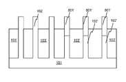
- silicon fins 102are formed, e.g. by etching, in a silicon wafer 101 .
- An oxide 103is filled between adjacent fins 102 .
- Fins 102may be formed to a width of 80 ⁇ to 800 ⁇ , for example 200 ⁇ , and to a depth of 800 ⁇ to 5000 ⁇ . e.g. 2000 ⁇ .
- the oxide 103may, for example, be formed of tetraethyl orthosilicate (TEOS), high aspect ratio process (HARP) material, or spin-on dielectric (SOD) material including a densification process.
- TEOStetraethyl orthosilicate
- HTPhigh aspect ratio process
- SODspin-on dielectric
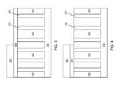
- the nitride layer 201may be formed to a thickness of 50 ⁇ to 100 ⁇ .
- a photo mask 301is formed on the nitride layer 201 , on a plurality of silicon fins 102 and on the oxide 103 therebetween.
- the photo mask 301is formed over and protects the permanent fins, and exposes areas where fins need to be removed.
- the nitride layer 201is then dry etched selectively against the underlying oxide 103 , leaving a first nitride liner 201 ′ beneath the photo mask 301 , as illustrated in FIG. 4 .
- the exposed silicon fins 102are dry etched to a depth of 500 ⁇ to 5000 ⁇ , e.g., 2000 ⁇ , resulting in etched silicon fins 102 ′.
- the dry etch chemistrymay be a sulfur hexafluoride (SF 6 ) based chemistry or a nitrogen trifluoride (NF 3 ) based chemistry.
- the dry etch processmay be followed by a short isotropic wet etch or a short silicon oxidation to remove any “stringers” that may have formed in overhanging areas in the trenches or as a result of small defects that block the dry etch process.
- the exposed silicon fins 102may be wet etched using a nitric acid (HNO 3 ) plus hyrdrofluoric (HF) acid or a tetramethylammonium hydroxide (TMAH).
- HNO 3nitric acid
- HFhyrdrofluoric
- TMAHtetramethylammonium hydroxide
- the photo mask 301is stripped off, as illustrated in FIG. 6 .
- the first nitride liner 201 ′is removed from the upper surface of the first plurality of silicon fins 201 , by a wet or dry etch. This avoids a step in the wafer 101 where the etched first nitride liner 201 ′ was previously located.
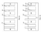
- a second nitride liner 801is formed on the upper surface of silicon fins 102 , the etched silicon fins 102 ′, and oxide 103 therebetween.
- the second nitride liner 801will completely fill the trenches above the etched silicon fins 102 ′ and is formed above silicon fins 102 and oxide 103 to a thickness of 75 percent of a width of one of the silicon fins 102 .
- the second nitride liner 801may be formed of furnace nitride, which yields better step coverage than PECVD nitride.
- removing the etched first nitride liner 201 ′avoids a step in the second nitride liner 801 .
- the second nitride liner 801is removed down to the upper surface of silicon fins 102 by dry etching or CMP. As a result, only nitride 801 ′ formed in the trenches on top of the etched silicon fins 102 ′ remains.
- the oxide 103 ′is recessed to a depth of 200 ⁇ to 400 ⁇ by atomic layer etching or wet etching with high selectivity to silicon and nitride. As a result, both the silicon fins 102 and the nitride fins 801 ′ are exposed. More specifically, the upper surface of the silicon fins 102 and an upper surface of the nitride fins 801 ′ are coplanar.
- Embodiments of the present disclosurecan achieve several technical effects including avoiding costly trench etching and trench filling and achieving a planar surface after removal of the unnecessary fins.
- Embodiments of the present disclosureenjoy utility in various industrial applications as, for example, microprocessors, smart phones, mobile phones, cellular handsets, set-top boxes, DVD recorders and players, automotive navigation, printers and peripherals, networking and telecom equipment, gaming systems, and digital cameras.
- the present disclosuretherefore enjoys industrial applicability in any of various types of highly integrated semiconductor devices including FinFETs.
Landscapes
- Weting (AREA)
- Insulated Gate Type Field-Effect Transistor (AREA)
Abstract
Description
Claims (17)
Priority Applications (1)
| Application Number | Priority Date | Filing Date | Title |
|---|---|---|---|
| US13/664,062US9054212B2 (en) | 2012-10-30 | 2012-10-30 | Fin etch and Fin replacement for FinFET integration |
Applications Claiming Priority (1)
| Application Number | Priority Date | Filing Date | Title |
|---|---|---|---|
| US13/664,062US9054212B2 (en) | 2012-10-30 | 2012-10-30 | Fin etch and Fin replacement for FinFET integration |
Publications (2)
| Publication Number | Publication Date |
|---|---|
| US20140117419A1 US20140117419A1 (en) | 2014-05-01 |
| US9054212B2true US9054212B2 (en) | 2015-06-09 |
Family
ID=50546224
Family Applications (1)
| Application Number | Title | Priority Date | Filing Date |
|---|---|---|---|
| US13/664,062ActiveUS9054212B2 (en) | 2012-10-30 | 2012-10-30 | Fin etch and Fin replacement for FinFET integration |
Country Status (1)
| Country | Link |
|---|---|
| US (1) | US9054212B2 (en) |
Cited By (4)
| Publication number | Priority date | Publication date | Assignee | Title |
|---|---|---|---|---|
| US20140070322A1 (en)* | 2012-09-13 | 2014-03-13 | Globalfoundries Inc. | Methods of forming different finfet devices with different threshold voltages and integrated circuit products containing such devices |
| US20160380051A1 (en)* | 2015-06-25 | 2016-12-29 | International Business Machines Corporation | Finfet devices |
| US20170207217A1 (en)* | 2015-12-16 | 2017-07-20 | Imec Vzw | Finfet having locally higher fin-to-fin pitch |
| US10593801B2 (en) | 2015-04-10 | 2020-03-17 | Samsung Electronics Co., Ltd. | Semiconductor devices and methods of fabricating the same |
Families Citing this family (9)
| Publication number | Priority date | Publication date | Assignee | Title |
|---|---|---|---|---|
| US9362386B2 (en) | 2013-02-27 | 2016-06-07 | Taiwan Semiconductor Manufacturing Company, Ltd. | FETs and methods for forming the same |
| US8987791B2 (en)* | 2013-02-27 | 2015-03-24 | Taiwan Semiconductor Manufacturing Company, Ltd. | FinFETs and methods for forming the same |
| US9704974B2 (en)* | 2015-04-16 | 2017-07-11 | Taiwan Semiconductor Manufacturing Co., Ltd. | Process of manufacturing Fin-FET device |
| US9666692B2 (en)* | 2015-07-31 | 2017-05-30 | Taiwan Semiconductor Manufacturing Company, Ltd. | Method of forming FinFET gate oxide |
| US9805987B2 (en)* | 2015-09-04 | 2017-10-31 | International Business Machines Corporation | Self-aligned punch through stopper liner for bulk FinFET |
| US9773871B2 (en)* | 2015-11-16 | 2017-09-26 | Taiwan Semiconductor Manufacturing Co., Ltd. | Fin field effect transistor and method for fabricating the same |
| US9620503B1 (en)* | 2015-11-16 | 2017-04-11 | Taiwan Semiconductor Manufacturing Co., Ltd. | Fin field effect transistor and method for fabricating the same |
| US9768072B1 (en)* | 2016-06-30 | 2017-09-19 | International Business Machines Corporation | Fabrication of a vertical fin field effect transistor with reduced dimensional variations |
| CN109786458B (en)* | 2017-11-13 | 2022-02-15 | 中芯国际集成电路制造(上海)有限公司 | Semiconductor device and method of forming the same |
Citations (21)
| Publication number | Priority date | Publication date | Assignee | Title |
|---|---|---|---|---|
| US20080105931A1 (en)* | 2006-11-08 | 2008-05-08 | Samsung Electronics Co., Ltd. | Semiconductor devices having Fin-type active areas and methods of manufacturing the same |
| US20110133292A1 (en)* | 2009-12-03 | 2011-06-09 | Taiwan Semiconductor Manufacturing Company, Ltd. | FinFETs with Multiple Fin Heights |
| US8476137B1 (en)* | 2012-02-10 | 2013-07-02 | Globalfoundries Inc. | Methods of FinFET height control |
| US8481410B1 (en)* | 2012-01-31 | 2013-07-09 | Globalfoundries Inc. | Methods of epitaxial FinFET |
| US20130244387A1 (en)* | 2012-03-14 | 2013-09-19 | Globalfoundries Inc. | Methods for fabricating integrated circuits |
| US20130270641A1 (en)* | 2012-04-12 | 2013-10-17 | Globalfoundries Inc. | Methods of forming finfet semiconductor devices so as to tune the threshold voltage of such devices |
| US20130320294A1 (en)* | 2011-12-23 | 2013-12-05 | Annalisa Cappellani | Common-substrate semiconductor devices having nanowires or semiconductor bodies with differing material orientation or composition |
| US20130330889A1 (en)* | 2012-06-06 | 2013-12-12 | Taiwan Semiconductor Manufacturing Company, Ltd. | Method of making a finfet device |
| US20140061793A1 (en)* | 2012-08-29 | 2014-03-06 | International Business Machines Corporation | Sublithographic width finfet employing solid phase epitaxy |
| US20140097518A1 (en)* | 2012-10-04 | 2014-04-10 | International Business Machines Corporation | Semiconductor alloy fin field effect transistor |
| US20140151766A1 (en)* | 2012-12-05 | 2014-06-05 | Imec | FinFET DEVICE WITH DUAL-STRAINED CHANNELS AND METHOD FOR MANUFACTURING THEREOF |
| US20140151814A1 (en)* | 2011-12-21 | 2014-06-05 | Martin D. Giles | Methods for forming fins for metal oxide semiconductor device structures |
| US20140353760A1 (en)* | 2013-05-31 | 2014-12-04 | Stmicroelectronics, Inc. | METHOD TO CO-INTEGRATE SiGe AND Si CHANNELS FOR FINFET DEVICES |
| US20140353767A1 (en)* | 2013-05-31 | 2014-12-04 | Stmicroelectronics, Inc. | Method for the formation of fin structures for finfet devices |
| US20140374829A1 (en)* | 2011-08-08 | 2014-12-25 | Kabushiki Kaisha Toshiba | Integrated circuit device and method for manufacturing same |
| US20150017781A1 (en)* | 2013-07-12 | 2015-01-15 | United Microelectronics Corp. | Method of forming shallow trench isolation structure |
| US20150024573A1 (en)* | 2013-07-17 | 2015-01-22 | Globalfoundries Inc. | Methods of forming replacement fins for a finfet semiconductor device by performing a replacement growth process |
| US8941153B2 (en)* | 2009-11-20 | 2015-01-27 | Taiwan Semiconductor Manufacturing Company, Ltd. | FinFETs with different fin heights |
| US20150028398A1 (en)* | 2013-07-29 | 2015-01-29 | International Business Machines Corporation | Dielectric filler fins for planar topography in gate level |
| US20150028454A1 (en)* | 2013-07-24 | 2015-01-29 | International Business Machines Corporation | Finfet structures having silicon germanium and silicon channels |
| US8951870B2 (en)* | 2013-03-14 | 2015-02-10 | International Business Machines Corporation | Forming strained and relaxed silicon and silicon germanium fins on the same wafer |
- 2012
- 2012-10-30USUS13/664,062patent/US9054212B2/enactiveActive
Patent Citations (21)
| Publication number | Priority date | Publication date | Assignee | Title |
|---|---|---|---|---|
| US20080105931A1 (en)* | 2006-11-08 | 2008-05-08 | Samsung Electronics Co., Ltd. | Semiconductor devices having Fin-type active areas and methods of manufacturing the same |
| US8941153B2 (en)* | 2009-11-20 | 2015-01-27 | Taiwan Semiconductor Manufacturing Company, Ltd. | FinFETs with different fin heights |
| US20110133292A1 (en)* | 2009-12-03 | 2011-06-09 | Taiwan Semiconductor Manufacturing Company, Ltd. | FinFETs with Multiple Fin Heights |
| US20140374829A1 (en)* | 2011-08-08 | 2014-12-25 | Kabushiki Kaisha Toshiba | Integrated circuit device and method for manufacturing same |
| US20140151814A1 (en)* | 2011-12-21 | 2014-06-05 | Martin D. Giles | Methods for forming fins for metal oxide semiconductor device structures |
| US20130320294A1 (en)* | 2011-12-23 | 2013-12-05 | Annalisa Cappellani | Common-substrate semiconductor devices having nanowires or semiconductor bodies with differing material orientation or composition |
| US8481410B1 (en)* | 2012-01-31 | 2013-07-09 | Globalfoundries Inc. | Methods of epitaxial FinFET |
| US8476137B1 (en)* | 2012-02-10 | 2013-07-02 | Globalfoundries Inc. | Methods of FinFET height control |
| US20130244387A1 (en)* | 2012-03-14 | 2013-09-19 | Globalfoundries Inc. | Methods for fabricating integrated circuits |
| US20130270641A1 (en)* | 2012-04-12 | 2013-10-17 | Globalfoundries Inc. | Methods of forming finfet semiconductor devices so as to tune the threshold voltage of such devices |
| US20130330889A1 (en)* | 2012-06-06 | 2013-12-12 | Taiwan Semiconductor Manufacturing Company, Ltd. | Method of making a finfet device |
| US20140061793A1 (en)* | 2012-08-29 | 2014-03-06 | International Business Machines Corporation | Sublithographic width finfet employing solid phase epitaxy |
| US20140097518A1 (en)* | 2012-10-04 | 2014-04-10 | International Business Machines Corporation | Semiconductor alloy fin field effect transistor |
| US20140151766A1 (en)* | 2012-12-05 | 2014-06-05 | Imec | FinFET DEVICE WITH DUAL-STRAINED CHANNELS AND METHOD FOR MANUFACTURING THEREOF |
| US8951870B2 (en)* | 2013-03-14 | 2015-02-10 | International Business Machines Corporation | Forming strained and relaxed silicon and silicon germanium fins on the same wafer |
| US20140353767A1 (en)* | 2013-05-31 | 2014-12-04 | Stmicroelectronics, Inc. | Method for the formation of fin structures for finfet devices |
| US20140353760A1 (en)* | 2013-05-31 | 2014-12-04 | Stmicroelectronics, Inc. | METHOD TO CO-INTEGRATE SiGe AND Si CHANNELS FOR FINFET DEVICES |
| US20150017781A1 (en)* | 2013-07-12 | 2015-01-15 | United Microelectronics Corp. | Method of forming shallow trench isolation structure |
| US20150024573A1 (en)* | 2013-07-17 | 2015-01-22 | Globalfoundries Inc. | Methods of forming replacement fins for a finfet semiconductor device by performing a replacement growth process |
| US20150028454A1 (en)* | 2013-07-24 | 2015-01-29 | International Business Machines Corporation | Finfet structures having silicon germanium and silicon channels |
| US20150028398A1 (en)* | 2013-07-29 | 2015-01-29 | International Business Machines Corporation | Dielectric filler fins for planar topography in gate level |
Cited By (19)
| Publication number | Priority date | Publication date | Assignee | Title |
|---|---|---|---|---|
| US20140070322A1 (en)* | 2012-09-13 | 2014-03-13 | Globalfoundries Inc. | Methods of forming different finfet devices with different threshold voltages and integrated circuit products containing such devices |
| US9564367B2 (en)* | 2012-09-13 | 2017-02-07 | Globalfoundries Inc. | Methods of forming different FinFET devices with different threshold voltages and integrated circuit products containing such devices |
| US11271110B2 (en) | 2015-04-10 | 2022-03-08 | Samsung Electronics Co., Ltd. | Semiconductor devices and methods of fabricating the same |
| US10593801B2 (en) | 2015-04-10 | 2020-03-17 | Samsung Electronics Co., Ltd. | Semiconductor devices and methods of fabricating the same |
| US9685507B2 (en)* | 2015-06-25 | 2017-06-20 | International Business Machines Corporation | FinFET devices |
| US10319640B2 (en) | 2015-06-25 | 2019-06-11 | International Business Machines Corporation | FinFET devices |
| US10014221B2 (en) | 2015-06-25 | 2018-07-03 | International Business Machines Corporation | FinFET devices |
| US10141402B2 (en) | 2015-06-25 | 2018-11-27 | International Business Machines Corporation | FinFET devices |
| US10157797B2 (en)* | 2015-06-25 | 2018-12-18 | International Business Machines Corporation | FinFET devices |
| US10224247B2 (en) | 2015-06-25 | 2019-03-05 | International Business Machines Corporation | FinFET devices |
| US10276658B2 (en) | 2015-06-25 | 2019-04-30 | International Business Machines Corporation | FinFET devices |
| US12376369B2 (en) | 2015-06-25 | 2025-07-29 | Adeia Semiconductor Solutions Llc | FinFET devices |
| US20160379892A1 (en)* | 2015-06-25 | 2016-12-29 | International Business Machines Corporation | Finfet devices |
| US10699962B2 (en) | 2015-06-25 | 2020-06-30 | Tessera, Inc. | FinFET devices |
| US11615988B2 (en) | 2015-06-25 | 2023-03-28 | Tessera, LLC | FinFET devices |
| US11145551B2 (en) | 2015-06-25 | 2021-10-12 | Tessera, Inc. | FinFET devices |
| US20160380051A1 (en)* | 2015-06-25 | 2016-12-29 | International Business Machines Corporation | Finfet devices |
| US11114435B2 (en)* | 2015-12-16 | 2021-09-07 | Imec Vzw | FinFET having locally higher fin-to-fin pitch |
| US20170207217A1 (en)* | 2015-12-16 | 2017-07-20 | Imec Vzw | Finfet having locally higher fin-to-fin pitch |
Also Published As
| Publication number | Publication date |
|---|---|
| US20140117419A1 (en) | 2014-05-01 |
Similar Documents
| Publication | Publication Date | Title |
|---|---|---|
| US9054212B2 (en) | Fin etch and Fin replacement for FinFET integration | |
| US9324713B1 (en) | Eliminating field oxide loss prior to FinFET source/drain epitaxial growth | |
| US10483169B2 (en) | FinFET cut-last process using oxide trench fill | |
| US11217678B2 (en) | Differential SG/EG spacer integration with equivalent NFET/PFET spacer widths and dual raised source drain expitaxial silicon and triple-nitride spacer integration enabling high-voltage EG device on FDSOI | |
| US9368496B1 (en) | Method for uniform recess depth and fill in single diffusion break for fin-type process and resulting devices | |
| US9123773B1 (en) | T-shaped single diffusion barrier with single mask approach process flow | |
| KR101598669B1 (en) | Fin deformation modulation | |
| US9960077B1 (en) | Ultra-scale gate cut pillar with overlay immunity and method for producing the same | |
| US8501607B1 (en) | FinFET alignment structures using a double trench flow | |
| US8518775B2 (en) | Integration of eNVM, RMG, and HKMG modules | |
| US9006067B2 (en) | Semiconductor device and method of fabricationg the same | |
| US20130277760A1 (en) | Dummy FinFET Structure and Method of Making Same | |
| US10211103B1 (en) | Advanced structure for self-aligned contact and method for producing the same | |
| US20130175622A1 (en) | Electrical isolation structures for ultra-thin semiconductor-on-insulator devices | |
| US9245979B2 (en) | FinFET semiconductor devices with local isolation features and methods for fabricating the same | |
| US9966313B2 (en) | FinFET device and method of manufacturing | |
| KR101745795B1 (en) | Semiconductor devices and methods of manufacture thereof | |
| US9356147B2 (en) | FinFET spacer etch for eSiGe improvement | |
| US20130224944A1 (en) | Methods for fabricating integrated circuits using tailored chamfered gate liner profiles | |
| US20120122303A1 (en) | Semiconductor structure having wide and narrow deep trenches with different materials | |
| US20100052048A1 (en) | Semiconductor device and method of manufacturing the same | |
| US9437674B2 (en) | Insulating trench forming method | |
| KR101025739B1 (en) | Method for manufacturing semiconductor device with neck-free vertical gate | |
| WO2014109087A1 (en) | Method for manufacturing semiconductor device | |
| US9875936B1 (en) | Spacer defined fin growth and differential fin width |
Legal Events
| Date | Code | Title | Description |
|---|---|---|---|
| AS | Assignment | Owner name:GLOBALFOUNDRIES INC., CAYMAN ISLANDS Free format text:ASSIGNMENT OF ASSIGNORS INTEREST;ASSIGNOR:JUENGLING, WERNER;REEL/FRAME:029215/0434 Effective date:20121016 | |
| FEPP | Fee payment procedure | Free format text:PAYOR NUMBER ASSIGNED (ORIGINAL EVENT CODE: ASPN); ENTITY STATUS OF PATENT OWNER: LARGE ENTITY | |
| STCF | Information on status: patent grant | Free format text:PATENTED CASE | |
| MAFP | Maintenance fee payment | Free format text:PAYMENT OF MAINTENANCE FEE, 4TH YEAR, LARGE ENTITY (ORIGINAL EVENT CODE: M1551); ENTITY STATUS OF PATENT OWNER: LARGE ENTITY Year of fee payment:4 | |
| AS | Assignment | Owner name:WILMINGTON TRUST, NATIONAL ASSOCIATION, DELAWARE Free format text:SECURITY AGREEMENT;ASSIGNOR:GLOBALFOUNDRIES INC.;REEL/FRAME:049490/0001 Effective date:20181127 | |
| AS | Assignment | Owner name:GLOBALFOUNDRIES U.S. INC., CALIFORNIA Free format text:ASSIGNMENT OF ASSIGNORS INTEREST;ASSIGNOR:GLOBALFOUNDRIES INC.;REEL/FRAME:054633/0001 Effective date:20201022 | |
| AS | Assignment | Owner name:GLOBALFOUNDRIES INC., CAYMAN ISLANDS Free format text:RELEASE BY SECURED PARTY;ASSIGNOR:WILMINGTON TRUST, NATIONAL ASSOCIATION;REEL/FRAME:054636/0001 Effective date:20201117 | |
| AS | Assignment | Owner name:GLOBALFOUNDRIES U.S. INC., NEW YORK Free format text:RELEASE BY SECURED PARTY;ASSIGNOR:WILMINGTON TRUST, NATIONAL ASSOCIATION;REEL/FRAME:056987/0001 Effective date:20201117 | |
| MAFP | Maintenance fee payment | Free format text:PAYMENT OF MAINTENANCE FEE, 8TH YEAR, LARGE ENTITY (ORIGINAL EVENT CODE: M1552); ENTITY STATUS OF PATENT OWNER: LARGE ENTITY Year of fee payment:8 |