US9054165B2 - Semiconductor devices including a through-substrate conductive member with an exposed end - Google Patents
Semiconductor devices including a through-substrate conductive member with an exposed endDownload PDFInfo
- Publication number
- US9054165B2 US9054165B2US13/468,655US201213468655AUS9054165B2US 9054165 B2US9054165 B2US 9054165B2US 201213468655 AUS201213468655 AUS 201213468655AUS 9054165 B2US9054165 B2US 9054165B2
- Authority
- US
- United States
- Prior art keywords
- substrate
- dielectric layer
- depressions
- sidewall
- back side
- Prior art date
- Legal status (The legal status is an assumption and is not a legal conclusion. Google has not performed a legal analysis and makes no representation as to the accuracy of the status listed.)
- Active
Links
Images


Classifications
- H—ELECTRICITY
- H01—ELECTRIC ELEMENTS
- H01L—SEMICONDUCTOR DEVICES NOT COVERED BY CLASS H10
- H01L23/00—Details of semiconductor or other solid state devices
- H01L23/52—Arrangements for conducting electric current within the device in operation from one component to another, i.e. interconnections, e.g. wires, lead frames
- H01L23/538—Arrangements for conducting electric current within the device in operation from one component to another, i.e. interconnections, e.g. wires, lead frames the interconnection structure between a plurality of semiconductor chips being formed on, or in, insulating substrates
- H01L23/5384—Conductive vias through the substrate with or without pins, e.g. buried coaxial conductors
- H—ELECTRICITY
- H01—ELECTRIC ELEMENTS
- H01L—SEMICONDUCTOR DEVICES NOT COVERED BY CLASS H10
- H01L21/00—Processes or apparatus adapted for the manufacture or treatment of semiconductor or solid state devices or of parts thereof
- H01L21/70—Manufacture or treatment of devices consisting of a plurality of solid state components formed in or on a common substrate or of parts thereof; Manufacture of integrated circuit devices or of parts thereof
- H01L21/71—Manufacture of specific parts of devices defined in group H01L21/70
- H01L21/768—Applying interconnections to be used for carrying current between separate components within a device comprising conductors and dielectrics
- H01L21/76898—Applying interconnections to be used for carrying current between separate components within a device comprising conductors and dielectrics formed through a semiconductor substrate
- H—ELECTRICITY
- H01—ELECTRIC ELEMENTS
- H01L—SEMICONDUCTOR DEVICES NOT COVERED BY CLASS H10
- H01L23/00—Details of semiconductor or other solid state devices
- H01L23/28—Encapsulations, e.g. encapsulating layers, coatings, e.g. for protection
- H01L23/29—Encapsulations, e.g. encapsulating layers, coatings, e.g. for protection characterised by the material, e.g. carbon
- H01L23/293—Organic, e.g. plastic
- H—ELECTRICITY
- H01—ELECTRIC ELEMENTS
- H01L—SEMICONDUCTOR DEVICES NOT COVERED BY CLASS H10
- H01L23/00—Details of semiconductor or other solid state devices
- H01L23/28—Encapsulations, e.g. encapsulating layers, coatings, e.g. for protection
- H01L23/31—Encapsulations, e.g. encapsulating layers, coatings, e.g. for protection characterised by the arrangement or shape
- H01L23/3157—Partial encapsulation or coating
- H—ELECTRICITY
- H01—ELECTRIC ELEMENTS
- H01L—SEMICONDUCTOR DEVICES NOT COVERED BY CLASS H10
- H01L23/00—Details of semiconductor or other solid state devices
- H01L23/52—Arrangements for conducting electric current within the device in operation from one component to another, i.e. interconnections, e.g. wires, lead frames
- H01L23/538—Arrangements for conducting electric current within the device in operation from one component to another, i.e. interconnections, e.g. wires, lead frames the interconnection structure between a plurality of semiconductor chips being formed on, or in, insulating substrates
- H01L23/5386—Geometry or layout of the interconnection structure
- H—ELECTRICITY
- H01—ELECTRIC ELEMENTS
- H01L—SEMICONDUCTOR DEVICES NOT COVERED BY CLASS H10
- H01L24/00—Arrangements for connecting or disconnecting semiconductor or solid-state bodies; Methods or apparatus related thereto
- H01L24/01—Means for bonding being attached to, or being formed on, the surface to be connected, e.g. chip-to-package, die-attach, "first-level" interconnects; Manufacturing methods related thereto
- H01L24/10—Bump connectors ; Manufacturing methods related thereto
- H01L24/15—Structure, shape, material or disposition of the bump connectors after the connecting process
- H01L24/17—Structure, shape, material or disposition of the bump connectors after the connecting process of a plurality of bump connectors
- H—ELECTRICITY
- H01—ELECTRIC ELEMENTS
- H01L—SEMICONDUCTOR DEVICES NOT COVERED BY CLASS H10
- H01L24/00—Arrangements for connecting or disconnecting semiconductor or solid-state bodies; Methods or apparatus related thereto
- H01L24/93—Batch processes
- H01L24/95—Batch processes at chip-level, i.e. with connecting carried out on a plurality of singulated devices, i.e. on diced chips
- H01L24/97—Batch processes at chip-level, i.e. with connecting carried out on a plurality of singulated devices, i.e. on diced chips the devices being connected to a common substrate, e.g. interposer, said common substrate being separable into individual assemblies after connecting
- H—ELECTRICITY
- H01—ELECTRIC ELEMENTS
- H01L—SEMICONDUCTOR DEVICES NOT COVERED BY CLASS H10
- H01L25/00—Assemblies consisting of a plurality of semiconductor or other solid state devices
- H01L25/03—Assemblies consisting of a plurality of semiconductor or other solid state devices all the devices being of a type provided for in a single subclass of subclasses H10B, H10D, H10F, H10H, H10K or H10N, e.g. assemblies of rectifier diodes
- H01L25/04—Assemblies consisting of a plurality of semiconductor or other solid state devices all the devices being of a type provided for in a single subclass of subclasses H10B, H10D, H10F, H10H, H10K or H10N, e.g. assemblies of rectifier diodes the devices not having separate containers
- H01L25/065—Assemblies consisting of a plurality of semiconductor or other solid state devices all the devices being of a type provided for in a single subclass of subclasses H10B, H10D, H10F, H10H, H10K or H10N, e.g. assemblies of rectifier diodes the devices not having separate containers the devices being of a type provided for in group H10D89/00
- H01L25/0655—Assemblies consisting of a plurality of semiconductor or other solid state devices all the devices being of a type provided for in a single subclass of subclasses H10B, H10D, H10F, H10H, H10K or H10N, e.g. assemblies of rectifier diodes the devices not having separate containers the devices being of a type provided for in group H10D89/00 the devices being arranged next to each other
- H—ELECTRICITY
- H01—ELECTRIC ELEMENTS
- H01L—SEMICONDUCTOR DEVICES NOT COVERED BY CLASS H10
- H01L25/00—Assemblies consisting of a plurality of semiconductor or other solid state devices
- H01L25/03—Assemblies consisting of a plurality of semiconductor or other solid state devices all the devices being of a type provided for in a single subclass of subclasses H10B, H10D, H10F, H10H, H10K or H10N, e.g. assemblies of rectifier diodes
- H01L25/04—Assemblies consisting of a plurality of semiconductor or other solid state devices all the devices being of a type provided for in a single subclass of subclasses H10B, H10D, H10F, H10H, H10K or H10N, e.g. assemblies of rectifier diodes the devices not having separate containers
- H01L25/065—Assemblies consisting of a plurality of semiconductor or other solid state devices all the devices being of a type provided for in a single subclass of subclasses H10B, H10D, H10F, H10H, H10K or H10N, e.g. assemblies of rectifier diodes the devices not having separate containers the devices being of a type provided for in group H10D89/00
- H01L25/0657—Stacked arrangements of devices
- H—ELECTRICITY
- H01—ELECTRIC ELEMENTS
- H01L—SEMICONDUCTOR DEVICES NOT COVERED BY CLASS H10
- H01L25/00—Assemblies consisting of a plurality of semiconductor or other solid state devices
- H01L25/50—Multistep manufacturing processes of assemblies consisting of devices, the devices being individual devices of subclass H10D or integrated devices of class H10
- H—ELECTRICITY
- H01—ELECTRIC ELEMENTS
- H01L—SEMICONDUCTOR DEVICES NOT COVERED BY CLASS H10
- H01L2224/00—Indexing scheme for arrangements for connecting or disconnecting semiconductor or solid-state bodies and methods related thereto as covered by H01L24/00
- H01L2224/01—Means for bonding being attached to, or being formed on, the surface to be connected, e.g. chip-to-package, die-attach, "first-level" interconnects; Manufacturing methods related thereto
- H01L2224/02—Bonding areas; Manufacturing methods related thereto
- H01L2224/04—Structure, shape, material or disposition of the bonding areas prior to the connecting process
- H01L2224/0401—Bonding areas specifically adapted for bump connectors, e.g. under bump metallisation [UBM]
- H—ELECTRICITY
- H01—ELECTRIC ELEMENTS
- H01L—SEMICONDUCTOR DEVICES NOT COVERED BY CLASS H10
- H01L2224/00—Indexing scheme for arrangements for connecting or disconnecting semiconductor or solid-state bodies and methods related thereto as covered by H01L24/00
- H01L2224/01—Means for bonding being attached to, or being formed on, the surface to be connected, e.g. chip-to-package, die-attach, "first-level" interconnects; Manufacturing methods related thereto
- H01L2224/02—Bonding areas; Manufacturing methods related thereto
- H01L2224/04—Structure, shape, material or disposition of the bonding areas prior to the connecting process
- H01L2224/05—Structure, shape, material or disposition of the bonding areas prior to the connecting process of an individual bonding area
- H01L2224/05001—Internal layers
- H01L2224/05005—Structure
- H01L2224/05009—Bonding area integrally formed with a via connection of the semiconductor or solid-state body
- H—ELECTRICITY
- H01—ELECTRIC ELEMENTS
- H01L—SEMICONDUCTOR DEVICES NOT COVERED BY CLASS H10
- H01L2224/00—Indexing scheme for arrangements for connecting or disconnecting semiconductor or solid-state bodies and methods related thereto as covered by H01L24/00
- H01L2224/01—Means for bonding being attached to, or being formed on, the surface to be connected, e.g. chip-to-package, die-attach, "first-level" interconnects; Manufacturing methods related thereto
- H01L2224/02—Bonding areas; Manufacturing methods related thereto
- H01L2224/04—Structure, shape, material or disposition of the bonding areas prior to the connecting process
- H01L2224/05—Structure, shape, material or disposition of the bonding areas prior to the connecting process of an individual bonding area
- H01L2224/0554—External layer
- H01L2224/0555—Shape
- H01L2224/05552—Shape in top view
- H—ELECTRICITY
- H01—ELECTRIC ELEMENTS
- H01L—SEMICONDUCTOR DEVICES NOT COVERED BY CLASS H10
- H01L2224/00—Indexing scheme for arrangements for connecting or disconnecting semiconductor or solid-state bodies and methods related thereto as covered by H01L24/00
- H01L2224/01—Means for bonding being attached to, or being formed on, the surface to be connected, e.g. chip-to-package, die-attach, "first-level" interconnects; Manufacturing methods related thereto
- H01L2224/02—Bonding areas; Manufacturing methods related thereto
- H01L2224/04—Structure, shape, material or disposition of the bonding areas prior to the connecting process
- H01L2224/05—Structure, shape, material or disposition of the bonding areas prior to the connecting process of an individual bonding area
- H01L2224/0554—External layer
- H01L2224/0556—Disposition
- H01L2224/0557—Disposition the external layer being disposed on a via connection of the semiconductor or solid-state body
- H—ELECTRICITY
- H01—ELECTRIC ELEMENTS
- H01L—SEMICONDUCTOR DEVICES NOT COVERED BY CLASS H10
- H01L2224/00—Indexing scheme for arrangements for connecting or disconnecting semiconductor or solid-state bodies and methods related thereto as covered by H01L24/00
- H01L2224/01—Means for bonding being attached to, or being formed on, the surface to be connected, e.g. chip-to-package, die-attach, "first-level" interconnects; Manufacturing methods related thereto
- H01L2224/02—Bonding areas; Manufacturing methods related thereto
- H01L2224/04—Structure, shape, material or disposition of the bonding areas prior to the connecting process
- H01L2224/05—Structure, shape, material or disposition of the bonding areas prior to the connecting process of an individual bonding area
- H01L2224/0554—External layer
- H01L2224/0556—Disposition
- H01L2224/05571—Disposition the external layer being disposed in a recess of the surface
- H01L2224/05572—Disposition the external layer being disposed in a recess of the surface the external layer extending out of an opening
- H—ELECTRICITY
- H01—ELECTRIC ELEMENTS
- H01L—SEMICONDUCTOR DEVICES NOT COVERED BY CLASS H10
- H01L2224/00—Indexing scheme for arrangements for connecting or disconnecting semiconductor or solid-state bodies and methods related thereto as covered by H01L24/00
- H01L2224/01—Means for bonding being attached to, or being formed on, the surface to be connected, e.g. chip-to-package, die-attach, "first-level" interconnects; Manufacturing methods related thereto
- H01L2224/10—Bump connectors; Manufacturing methods related thereto
- H01L2224/12—Structure, shape, material or disposition of the bump connectors prior to the connecting process
- H01L2224/13—Structure, shape, material or disposition of the bump connectors prior to the connecting process of an individual bump connector
- H01L2224/13001—Core members of the bump connector
- H01L2224/1302—Disposition
- H01L2224/13023—Disposition the whole bump connector protruding from the surface
- H—ELECTRICITY
- H01—ELECTRIC ELEMENTS
- H01L—SEMICONDUCTOR DEVICES NOT COVERED BY CLASS H10
- H01L2224/00—Indexing scheme for arrangements for connecting or disconnecting semiconductor or solid-state bodies and methods related thereto as covered by H01L24/00
- H01L2224/01—Means for bonding being attached to, or being formed on, the surface to be connected, e.g. chip-to-package, die-attach, "first-level" interconnects; Manufacturing methods related thereto
- H01L2224/10—Bump connectors; Manufacturing methods related thereto
- H01L2224/12—Structure, shape, material or disposition of the bump connectors prior to the connecting process
- H01L2224/13—Structure, shape, material or disposition of the bump connectors prior to the connecting process of an individual bump connector
- H01L2224/13001—Core members of the bump connector
- H01L2224/1302—Disposition
- H01L2224/13025—Disposition the bump connector being disposed on a via connection of the semiconductor or solid-state body
- H—ELECTRICITY
- H01—ELECTRIC ELEMENTS
- H01L—SEMICONDUCTOR DEVICES NOT COVERED BY CLASS H10
- H01L2224/00—Indexing scheme for arrangements for connecting or disconnecting semiconductor or solid-state bodies and methods related thereto as covered by H01L24/00
- H01L2224/01—Means for bonding being attached to, or being formed on, the surface to be connected, e.g. chip-to-package, die-attach, "first-level" interconnects; Manufacturing methods related thereto
- H01L2224/10—Bump connectors; Manufacturing methods related thereto
- H01L2224/15—Structure, shape, material or disposition of the bump connectors after the connecting process
- H01L2224/16—Structure, shape, material or disposition of the bump connectors after the connecting process of an individual bump connector
- H01L2224/161—Disposition
- H01L2224/16135—Disposition the bump connector connecting between different semiconductor or solid-state bodies, i.e. chip-to-chip
- H01L2224/16145—Disposition the bump connector connecting between different semiconductor or solid-state bodies, i.e. chip-to-chip the bodies being stacked
- H01L2224/16146—Disposition the bump connector connecting between different semiconductor or solid-state bodies, i.e. chip-to-chip the bodies being stacked the bump connector connecting to a via connection in the semiconductor or solid-state body
- H—ELECTRICITY
- H01—ELECTRIC ELEMENTS
- H01L—SEMICONDUCTOR DEVICES NOT COVERED BY CLASS H10
- H01L2224/00—Indexing scheme for arrangements for connecting or disconnecting semiconductor or solid-state bodies and methods related thereto as covered by H01L24/00
- H01L2224/93—Batch processes
- H01L2224/95—Batch processes at chip-level, i.e. with connecting carried out on a plurality of singulated devices, i.e. on diced chips
- H01L2224/97—Batch processes at chip-level, i.e. with connecting carried out on a plurality of singulated devices, i.e. on diced chips the devices being connected to a common substrate, e.g. interposer, said common substrate being separable into individual assemblies after connecting
- H—ELECTRICITY
- H01—ELECTRIC ELEMENTS
- H01L—SEMICONDUCTOR DEVICES NOT COVERED BY CLASS H10
- H01L2225/00—Details relating to assemblies covered by the group H01L25/00 but not provided for in its subgroups
- H01L2225/03—All the devices being of a type provided for in the same main group of the same subclass of class H10, e.g. assemblies of rectifier diodes
- H01L2225/04—All the devices being of a type provided for in the same main group of the same subclass of class H10, e.g. assemblies of rectifier diodes the devices not having separate containers
- H01L2225/065—All the devices being of a type provided for in the same main group of the same subclass of class H10
- H01L2225/06503—Stacked arrangements of devices
- H01L2225/06513—Bump or bump-like direct electrical connections between devices, e.g. flip-chip connection, solder bumps
- H—ELECTRICITY
- H01—ELECTRIC ELEMENTS
- H01L—SEMICONDUCTOR DEVICES NOT COVERED BY CLASS H10
- H01L2225/00—Details relating to assemblies covered by the group H01L25/00 but not provided for in its subgroups
- H01L2225/03—All the devices being of a type provided for in the same main group of the same subclass of class H10, e.g. assemblies of rectifier diodes
- H01L2225/04—All the devices being of a type provided for in the same main group of the same subclass of class H10, e.g. assemblies of rectifier diodes the devices not having separate containers
- H01L2225/065—All the devices being of a type provided for in the same main group of the same subclass of class H10
- H01L2225/06503—Stacked arrangements of devices
- H01L2225/06541—Conductive via connections through the device, e.g. vertical interconnects, through silicon via [TSV]
- H—ELECTRICITY
- H01—ELECTRIC ELEMENTS
- H01L—SEMICONDUCTOR DEVICES NOT COVERED BY CLASS H10
- H01L24/00—Arrangements for connecting or disconnecting semiconductor or solid-state bodies; Methods or apparatus related thereto
- H01L24/01—Means for bonding being attached to, or being formed on, the surface to be connected, e.g. chip-to-package, die-attach, "first-level" interconnects; Manufacturing methods related thereto
- H01L24/02—Bonding areas ; Manufacturing methods related thereto
- H01L24/03—Manufacturing methods
- H—ELECTRICITY
- H01—ELECTRIC ELEMENTS
- H01L—SEMICONDUCTOR DEVICES NOT COVERED BY CLASS H10
- H01L24/00—Arrangements for connecting or disconnecting semiconductor or solid-state bodies; Methods or apparatus related thereto
- H01L24/01—Means for bonding being attached to, or being formed on, the surface to be connected, e.g. chip-to-package, die-attach, "first-level" interconnects; Manufacturing methods related thereto
- H01L24/02—Bonding areas ; Manufacturing methods related thereto
- H01L24/04—Structure, shape, material or disposition of the bonding areas prior to the connecting process
- H01L24/05—Structure, shape, material or disposition of the bonding areas prior to the connecting process of an individual bonding area
- H—ELECTRICITY
- H01—ELECTRIC ELEMENTS
- H01L—SEMICONDUCTOR DEVICES NOT COVERED BY CLASS H10
- H01L24/00—Arrangements for connecting or disconnecting semiconductor or solid-state bodies; Methods or apparatus related thereto
- H01L24/01—Means for bonding being attached to, or being formed on, the surface to be connected, e.g. chip-to-package, die-attach, "first-level" interconnects; Manufacturing methods related thereto
- H01L24/10—Bump connectors ; Manufacturing methods related thereto
- H01L24/15—Structure, shape, material or disposition of the bump connectors after the connecting process
- H01L24/16—Structure, shape, material or disposition of the bump connectors after the connecting process of an individual bump connector
- H—ELECTRICITY
- H01—ELECTRIC ELEMENTS
- H01L—SEMICONDUCTOR DEVICES NOT COVERED BY CLASS H10
- H01L2924/00—Indexing scheme for arrangements or methods for connecting or disconnecting semiconductor or solid-state bodies as covered by H01L24/00
- H01L2924/0001—Technical content checked by a classifier
- H01L2924/00012—Relevant to the scope of the group, the symbol of which is combined with the symbol of this group
- H—ELECTRICITY
- H01—ELECTRIC ELEMENTS
- H01L—SEMICONDUCTOR DEVICES NOT COVERED BY CLASS H10
- H01L2924/00—Indexing scheme for arrangements or methods for connecting or disconnecting semiconductor or solid-state bodies as covered by H01L24/00
- H01L2924/0001—Technical content checked by a classifier
- H01L2924/00014—Technical content checked by a classifier the subject-matter covered by the group, the symbol of which is combined with the symbol of this group, being disclosed without further technical details
- H—ELECTRICITY
- H01—ELECTRIC ELEMENTS
- H01L—SEMICONDUCTOR DEVICES NOT COVERED BY CLASS H10
- H01L2924/00—Indexing scheme for arrangements or methods for connecting or disconnecting semiconductor or solid-state bodies as covered by H01L24/00
- H01L2924/0001—Technical content checked by a classifier
- H01L2924/0002—Not covered by any one of groups H01L24/00, H01L24/00 and H01L2224/00
- H—ELECTRICITY
- H01—ELECTRIC ELEMENTS
- H01L—SEMICONDUCTOR DEVICES NOT COVERED BY CLASS H10
- H01L2924/00—Indexing scheme for arrangements or methods for connecting or disconnecting semiconductor or solid-state bodies as covered by H01L24/00
- H01L2924/01—Chemical elements
- H01L2924/01005—Boron [B]
- H—ELECTRICITY
- H01—ELECTRIC ELEMENTS
- H01L—SEMICONDUCTOR DEVICES NOT COVERED BY CLASS H10
- H01L2924/00—Indexing scheme for arrangements or methods for connecting or disconnecting semiconductor or solid-state bodies as covered by H01L24/00
- H01L2924/01—Chemical elements
- H01L2924/01006—Carbon [C]
- H—ELECTRICITY
- H01—ELECTRIC ELEMENTS
- H01L—SEMICONDUCTOR DEVICES NOT COVERED BY CLASS H10
- H01L2924/00—Indexing scheme for arrangements or methods for connecting or disconnecting semiconductor or solid-state bodies as covered by H01L24/00
- H01L2924/01—Chemical elements
- H01L2924/01033—Arsenic [As]
- H—ELECTRICITY
- H01—ELECTRIC ELEMENTS
- H01L—SEMICONDUCTOR DEVICES NOT COVERED BY CLASS H10
- H01L2924/00—Indexing scheme for arrangements or methods for connecting or disconnecting semiconductor or solid-state bodies as covered by H01L24/00
- H01L2924/01—Chemical elements
- H01L2924/01082—Lead [Pb]
- H—ELECTRICITY
- H01—ELECTRIC ELEMENTS
- H01L—SEMICONDUCTOR DEVICES NOT COVERED BY CLASS H10
- H01L2924/00—Indexing scheme for arrangements or methods for connecting or disconnecting semiconductor or solid-state bodies as covered by H01L24/00
- H01L2924/013—Alloys
- H01L2924/014—Solder alloys
- H—ELECTRICITY
- H01—ELECTRIC ELEMENTS
- H01L—SEMICONDUCTOR DEVICES NOT COVERED BY CLASS H10
- H01L2924/00—Indexing scheme for arrangements or methods for connecting or disconnecting semiconductor or solid-state bodies as covered by H01L24/00
- H01L2924/10—Details of semiconductor or other solid state devices to be connected
- H01L2924/11—Device type
- H01L2924/14—Integrated circuits
Definitions
- the present inventionis related to semiconductor devices and methods for manufacturing semiconductor devices suitable for stacked die packages and other applications.
- the individual dies(e.g., devices) generally include integrated circuits and a plurality of bond-pads coupled to the integrated circuits.
- the bond-padsprovide external contacts through which supply voltage, electrical signals, and other input/output parameters are transmitted to/from the integrated circuits.
- the bond-padsare usually very small, and they are typically arranged in dense arrays having a fine pitch between bond-pads.
- the wafers and diescan also be quite delicate. As a result, the dies are packaged for protection and to provide terminals that can be reliably connected to printed circuit boards.
- Such interconnectscan electrically couple bond-pads or other conductive elements at a front side of the dies to conductive elements at the back side of the dies.
- Through-substrate interconnectsfor example, are constructed by forming deep vias at the front side of the workpiece in alignment with corresponding bond-pads. The vias are often blind vias in that they are closed at one end within the workpiece. The blind vias are then lined with a dielectric material and filled with a conductive fill material. The workpiece is thinned from the back side to expose the interconnects and reduce the thickness of the final dies. Solder balls or other external electrical connectors are subsequently attached to the through-substrate interconnects at the back side and/or the front side of the workpiece. The external connectors can be attached to the interconnects either before or after singulating the dies from the workpiece.
- Conventional processes for forming external connectors on through-substrate interconnects at the back side of the workpieceinclude (a) depositing a dielectric layer on the back side of the workpiece, (b) forming a photo-resist layer on the dielectric layer, (c) patterning and developing the photo-resist layer, (d) etching completely through the dielectric layer to form holes aligned with corresponding interconnects, (e) removing the photo-resist layer from the workpiece, and (f) forming external connectors on the interconnects located in the holes in the dielectric layer.
- One concern with forming external connectors on the back side of a workpieceis that conventional processes are relatively expensive because patterning the photo-resist layer requires expensive and time-consuming photolithography equipment and processes to achieve the tolerances required in semiconductor devices.
- FIG. 1is a schematic cross-sectional view of a portion of a semiconductor wafer with semiconductor devices in accordance with an embodiment of the technology.
- FIGS. 2A-2Fare schematic cross-sectional views illustrating embodiments of stages of a method for fabricating semiconductor devices.
- FIGS. 3A and 3Bare schematic cross-sectional views illustrating stages of an embodiment of another method for fabricating semiconductor devices.
- FIGS. 4A-4Care top plan views of different embodiments of semiconductor devices.
- FIG. 5is a flow chart illustrating an embodiment of a method for fabricating semiconductor devices.
- FIG. 6is a flow chart illustrating another embodiment of a method for fabricating semiconductor devices.
- FIG. 7is a flow chart illustrating another embodiment of a method for fabricating semiconductor devices.
- FIG. 8is a schematic cross-sectional view illustrating an embodiment of a stacked-die assembly.
- FIGS. 9A and 9Bare schematic cross-sectional views illustrating stages of an embodiment of another method for fabricating semiconductor devices.
- FIG. 10is a schematic illustration of a system including semiconductor devices.
- semiconductor devicesare manufactured on and/or in semiconductor wafers that can include substrates upon which and/or in which microelectronic devices, micromechanical devices, data storage elements, optics, read/write components, and other features are fabricated.
- SRAMstatic random access memory
- DRAMdynamic random access memory
- flash memorye.g., NAND flash-memory
- processorsimagers, and other types of devices can be constructed on semiconductor wafers.
- FIG. 1is a schematic cross-sectional view illustrating a portion of an embodiment of a semiconductor wafer 100 .
- the semiconductor wafer 100includes a semiconductor substrate 102 having a first surface 104 and a second surface 106 .
- the semiconductor substrate 102can be formed from silicon, gallium arsenide, or other suitable semiconductive materials.
- the wafer 100also includes a plurality of semiconductor dies 110 (e.g., devices) formed on and/or in the semiconductor substrate 102 .
- the dies 110are arranged in a die pattern across the semiconductor substrate 102 such that the dies 110 are spaced apart by cutting lanes C-C. For purposes of illustration, only two dies 110 are illustrated in FIG.
- Individual dies 110include integrated circuitry 112 , a plurality of first external contact sites 114 at the first surface 104 of the substrate 102 , and a plurality of second external contact sites 116 at least proximate to the second surface 106 of the substrate 102 .
- the dies 110can further include a plurality of conductive features 120 electrically coupled to the integrated circuitry 112 , the first external contact sites 114 , and the second external contact sites 116 .
- the particular embodiment of the conductive features 120 illustrated in FIG. 1are through-substrate interconnects.
- the conductive features 120have first ends 122 at the first external contact sites 114 and second ends 124 defining the second external contact sites 116 .
- the second ends 124 of the conductive features 120can be offset from the second surface 106 of the substrate 102 .
- the second ends 124 of the conductive features 120can project outwardly or otherwise away from the second surface 106 of the substrate such that the tips of the second ends 124 are spaced apart from the second surface 106 by an offset distance O.
- the semiconductor wafer 100can further include a dielectric layer 130 at the second surface 106 of the substrate 102 .
- the dielectric layer 130can be composed of a polymeric material or another suitable dielectric material for protecting the second surface 106 of the substrate 102 .
- the dielectric layer 130for example, can be composed of a photo-imageable polymer, such as a photo-imageable polyimide.
- the dielectric layer 130has a plurality of depressions 132 at the second external contact sites 116 . The depressions extend to a depth D at an intermediate level within the dielectric layer 130 such that at least the tips of the second ends 124 of the conductive features 120 are exposed within the depressions 132 .
- the depressions 132have bottom surfaces 134 at the intermediate depth D such that the bottom surfaces 134 are below the tips of the second ends 124 of the conductive features 120 but above the second surface 106 of the substrate 102 .
- the depth that the depressions 132 extend into the dielectric layer 130is accordingly less than the total thickness T of the dielectric layer 130 such that a portion of the dielectric layer 130 remains on the second surface 106 of the substrate 102 at the depressions 132 .
- the portions of the second surface 106 aligned with the depressions 132 and adjacent to the conductive features 120are not exposed within the depressions 132 , but at least a portion of the second ends 124 of the conductive features 120 are exposed within the depressions 132 .
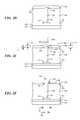
- FIGS. 2A-2Fillustrate stages of forming a portion of one of the semiconductor dies 110 noted by the dotted lines in FIG. 1 .
- the substrate 102is mounted to a carrier film 210 by an adhesive 212 at the first surface 104 .
- the substrate 102is at a full thickness at this stage, and the conductive feature 120 has been formed in a blind hole such that the second end 124 of the conductive feature 120 is at an intermediate elevation I within the substrate 102 .
- Suitable methods for forming the conductive feature 120are disclosed in U.S. patent application Ser. Nos. 10/925,501; 11/056,211; 11/217,877; and 11/215,214, all of which are incorporated by reference herein in their entirety.
- FIG. 2Billustrates a stage after the substrate 102 has been thinned from the full thickness illustrated in FIG. 2A to at least the intermediate elevation I ( FIG. 2A ) to form a thinned surface 214 at which the second end 124 of the conductive feature 120 is exposed or very nearly exposed.
- the substrate 102has been thinned to the extent that the second end 124 of the conductive feature 120 is exposed at the thinned surface 214 .
- the substrate 102can be thinned to a thinned surface 214 ′ (shown in dashed lines) spaced apart from the second end 124 of the conductive feature 120 by a small distance such that the second end 124 is not exposed at this stage.
- the substrate 102can be thinned using back-grinding, chemical-mechanical planarizing, or other suitable techniques for efficiently and accurately removing material from the substrate 102 .
- FIG. 2Cillustrates a subsequent stage in which material has been removed from the thinned surface 214 illustrated in FIG. 2B to form the second surface 106 of the substrate at an elevation that is spaced apart from the second end 124 of the conductive feature 120 .
- a tip 221 of the second end 124can be spaced apart or otherwise offset from the second surface 106 by the offset distance O explained above with respect to FIG. 1 .
- the materialcan be removed from the thinned surface 214 illustrated in FIG. 2B to form the second surface 106 of the substrate 102 shown in FIG. 2C by etching or otherwise removing material from the substrate 102 without removing as much material from the second end 124 of the conductive feature 120 . Suitable processes for selectively etching silicon or other semiconductor materials are known in the art.
- FIGS. 2D-2Fillustrate additional stages of methods for fabricating semiconductor devices.
- FIG. 2Dillustrates a stage after a dielectric material has been deposited onto the second surface 106 of the substrate 102 to form the dielectric layer 130 .
- the dielectric materialcan be deposited using spin-on, electrochemical deposition (e.g., electrophoretic resists), or other suitable techniques for depositing the dielectric material onto the second surface 106 .
- the dielectric layer 130also covers the second end 124 of the conductive feature 120 .
- the dielectric material of the dielectric layer 130can be a photo-imageable polymer or other suitable dielectric material for protecting the second surface 106 of the substrate 102 .
- FIG. 2Eillustrates a subsequent stage including irradiating areas of the dielectric layer 130 at the second ends 124 of the conductive features 120 to form photo-reacted material 250 (illustrated in dotted lines) in the dielectric layer 130 .
- the photo-reacted material 250 shown in FIG. 2Eextends to at least approximately the depth D in the dielectric layer 130 .
- the dielectric layer 130has a remaining thickness T r between the second surface 106 and the photo-reacted material 250 .
- the photo-reacted material 250can be formed by positioning a mask 260 relative to the substrate 102 such that openings 262 in the mask 260 are at least generally aligned with the second ends 124 of corresponding conductive features 120 .
- the portions of the dielectric layer 130 aligned with the openings 262are irradiated at an energy level E less than the minimum energy level E 0 required for the radiation to photo-chemically react the dielectric material through the full thickness T of the dielectric layer 130 .
- the photo-reacted material 250extends to only the intermediate depth D within the dielectric layer 130 instead of the full thickness T of the dielectric layer 130 .
- the relative dosage level for exposing or otherwise irradiating the dielectric materialcan be selected according to several parameters.
- the energy level Efor example, can be the lowest amount of energy that forms a photo-reacted region with sufficient depth to be at or below the tip 221 of the second end 124 of the conductive feature 120 .
- the energy level Ecan be approximately 20-50% of E 0 .
- the energy level Ecan be less than approximately 80% of the energy E 0 , less than approximately 50% of E 0 , or 10% to 80% of E 0 .
- FIG. 2Fillustrates a stage in which one of the depressions 132 is formed in the dielectric layer 130 by removing the photo-reacted material 250 ( FIG. 2E ) from the dielectric layer 130 .
- the depression 132can be formed by developing the photo-reacted region of the dielectric layer 130 with a suitable solution that dissolves the photo-reacted region selectively relative to the unreacted portions of the dielectric layer 130 and the material of the conductive feature 120 .
- the depression 132exposes at least a portion of the second end 124 of the conductive feature 120 without exposing the second surface 106 of the substrate 102 .
- the floor or bottom surface 134 of the depression 132can be spaced apart from the second surface 106 of the substrate 102 by approximately the remaining thickness T r ( FIG.
- the depression 132 and the second end 124 of the conductive feature 120accordingly define the second external contact site 116 associated with this conductive feature 120 .
- the depression 132has a cross-sectional dimension W 1 greater than a cross-sectional dimension W 2 of the conductive feature 120 .
- the depression 132can have other cross-sectional dimensions that are equal to or less than the cross-sectional dimension W 2 of the conductive feature 120 .
- the ability to use a larger cross-sectional dimension for the depression 132 compared to the cross-sectional dimension of the conductive feature 120makes it easier to align the openings in the mask 260 ( FIG. 2E ) with the conductive features 120 .
- the carrier film 210 and adhesive 212can be removed from the first surface 104 , and then solder balls, wire bonds, or other types of connectors can be attached to the first and second external contact sites 114 and 116 .
- FIGS. 2A-2Fcan cost-effectively form stackable dies and inhibit metal shorting to the substrate.
- the alignment tolerance between the openings 262 in the mask 260 ( FIG. 2E ) and the conductive features 120can be relatively large to mitigate alignment concerns.
- the second external contact sites 116eliminate the possibility of shorting between the substrate 102 and solder balls or other conductive connectors attached to the second ends 124 of the conductive features 120 .
- FIGS. 3A and 3Billustrate stages of another method for forming a semiconductor device.
- FIG. 3Amore specifically, illustrates a stage similar to the stages illustrated in FIGS. 2D and 2E explained above.
- the dielectric layer 130is irradiated at the second end 124 of the conductive feature 120 using a laser L instead of a micro-lithography process.
- the laser Lablates or otherwise removes the portion of the dielectric layer 130 covering the second end 124 of the conductive feature 120 .
- the dielectric layer 130 in this embodimenttherefore, does not need to be a photo-imageable polymer or other type of a photo-imageable material.
- the dielectric layer 130can instead be any suitable material that can be removed using a suitable laser.
- FIG. 3Billustrates a stage after which the laser L has formed a depression 132 in the dielectric layer 130 to expose at least a portion of the second end 124 of the conductive feature 120 . The exposed portion of the second end 124 in the depression 132 accordingly defines one of the second external contact sites 116 .
- FIGS. 4A-4Cillustrate various types of depressions formed relative to the second ends 124 of the conductive features 120
- like reference numbersrefer to like components in FIGS. 4A-4C
- FIG. 4Amore specifically, illustrates an embodiment in which discrete depressions 132 a are formed at corresponding conductive members 120 .
- the depressions 132 acan be circular, rectilinear, or any other suitable shape to expose the individual conductive members 120 .
- FIG. 4Billustrates an alternative embodiment in which individual depressions 132 b expose a plurality of second ends 124 of separate conductive features 120 .
- the depressions 132 bcan be long trenches aligned with the second ends 124 of a plurality of conductive features 120 along one direction Y relative to the wafer.
- FIG. 4Cillustrates another embodiment in which the individual depressions 132 c extend along a direction X of the wafer relative to the depressions 132 b illustrated in FIG. 4B .
- FIG. 5is a flow chart illustrating an embodiment of a method 500 for fabricating a semiconductor device.
- the method 500can include forming a conductive feature extending through a semiconductor substrate such that the conductive feature has an end projecting outwardly from a surface of the substrate (block 510 ).
- the method 500can further include forming a dielectric layer over the surface of the substrate and the end of the conductive feature (block 520 ) and forming a recess (e.g., a depression) in the dielectric layer (block 530 ).
- the recessfor example, can extend to an intermediate depth within the dielectric layer such that at least a portion of the end of the conductive feature is in the recess.
- FIG. 6is a flow chart of an embodiment of another method 600 for fabricating a semiconductor device.
- the method 600can include constructing a plurality of conductive features, such as interconnects in a semiconductor substrate (block 610 ).
- the interconnectscan be constructed such that individual interconnects have a first end electrically coupled to a bond site at a first surface of a substrate and a second end projecting away from a second surface of the substrate.
- the second end of the interconnectcan project away from the second surface of the substrate such that a tip of the second end of the interconnect is non-planar relative to the second surface of the substrate (e.g., offset from the second surface 106 ).
- the method 600can further include depositing a photosensitive or otherwise photo-reactive dielectric layer over the second surface of the substrate and the second ends of the interconnects (block 620 ).
- the methodcan also include irradiating areas of the dielectric layer at the second ends of the interconnects to form a plurality of photo-reacted regions in the dielectric layer (block 630 ) and removing the photo-reacted regions such that at least a portion of the second ends of the interconnects are exposed (block 640 ).
- the process of irradiating areas of the dielectric layercan include forming the photo-reacted regions such that the photo-reacted regions extend to a depth in the dielectric layer less than the thickness of the dielectric layer.
- FIG. 7is a flow chart of an embodiment of another method 700 for fabricating a semiconductor device.
- the method 700can include forming conductive features in a semiconductor substrate (block 710 ) such that the conductive features have first contact ends at bond sites and second contact ends spaced apart from the first contact ends.
- the method 700can further include offsetting the second contact ends of the conductive features from a surface of the semiconductor substrate (block 720 ) and covering the surface of the substrate and the second contact ends of the conductive features with a dielectric material (block 730 ).
- the method 700can also include exposing the contact ends of the conductive features by forming depressions in the dielectric material (block 740 ). For example, the depressions can be formed to be at least as large as the second contact ends without exposing the surface of the substrate through the depressions.
- FIG. 8is a schematic cross-sectional view of a stacked-die assembly 800 having a first semiconductor die 110 a and a second semiconductor device 110 b stacked on the first semiconductor die 110 a.
- the first and second semiconductor dies 110 a - bcan be similar to the semiconductor dies 110 described above with respect to FIG. 1 , and therefore like reference numbers refer to like components in FIGS. 1 and 8 .
- the stacked-die assembly 800can be formed by depositing first connectors 801 onto the first external contact sites 114 of the first semiconductor die 110 a and disposing second connectors 802 between the second ends 124 of the conductive features 120 of the first semiconductor die 110 a and the first external contact sites 114 of the second semiconductor die 110 b.
- the second connectors 802can be solder balls or other types of electrical links that are deposited or otherwise formed on either the second ends 124 of the conductive features 120 of the first semiconductor die 110 a or the first external contact sites 114 of the second semiconductor die 110 b.
- the first and second semiconductor dies 110 a - bare then aligned and positioned so that the second connectors 802 electrically couple the conductive features 120 of the first semiconductor die 110 a with corresponding conductive features 120 of the second semiconductor die 110 b.
- FIGS. 9A and 9Bare schematic cross-sectional views of stages of another embodiment for fabricating semiconductor devices, and like reference numbers refer to like components and procedures in FIGS. 1-9B .
- FIG. 9Aillustrates globally irradiating the dielectric layer 130 at an energy level E less than the energy level E 0 using a lamp to form a stratum of photo-reacted material 950 (illustrated in dotted lines) at an intermediate depth completely across the dielectric layer 130 .
- the photo-reacted material 950 shown in FIG. 9Ais similar to the photo-reacted region shown in FIG. 2E , and thus the photo-reacted material 950 extends to at least approximately the depth D in the dielectric layer 130 .
- the dielectric layer 130has a remaining thickness T r between the second surface 106 and the photo-reacted material 950 .
- the irradiation procedure in FIG. 9Ais a global flood exposure procedure that exposes large areas and even the full surface area of the dielectric layer 130 without using a mask or micro-lithography equipment.
- Suitable systems for exposing the dielectric layer 130include ultraviolet lamps, such as the UVEX UV tool, as an alternative to stepper or scanner tools used in micro-lithography processes.
- the relative dosage level for exposing or otherwise irradiating the dielectric materialcan be selected according to several parameters.
- the applied energy level Ecan be the lowest amount of energy that forms the photo-reacted region with sufficient depth to be at or below the tip 221 of the second end 124 of the conductive feature 120 .
- the energy level Ecan be approximately 20-50% of E 0 , but in other embodiments the energy level E can be less than approximately 80% of the energy level E 0 , less than approximately 50% of E 0 , or 10% to 80% of E 0 .
- FIG. 9Billustrates a subsequent stage in which the stratum of photo-reacted material 950 has been stripped or otherwise removed completely across the substrate to expose the second ends 124 of the conductive features 120 .
- the photo-reacted material 950can be removed by developing the photo-reacted material 950 to clear the portion of the dielectric layer 130 above the second ends 124 .
- the remaining thickness of the dielectric layeraccordingly covers the second side of the surface of the substrate adjacent to the second ends of the conductive features 120 and across other regions of the substrate surface.
- the second ends 124define the external contact sites at the second side or back side of the wafer. After forming the external contact sites, solder balls or other electrical connectors can be formed at the second ends 124 of the conductive features 120 .
- the embodiment of the method shown in FIGS. 9A and 9Bprovides a fast, low-cost process for forming external contact sites at through-substrate interconnects or other types of interconnects.
- several examples of the method shown in FIGS. 9A and 9Buse a flood lamp instead of micro-lithography equipment to increase the number of wafers that can be processed per hour and reduce the use of expensive micro-lithography equipment.
- any one of the semiconductor components described above with reference to FIGS. 1-10can be incorporated into any of a myriad of larger and/or more complex systems, a representative example of which is system 1000 shown schematically in FIG. 10 .
- the system 1000can include a processor 1001 , a memory 1002 (e.g., SRAM, DRAM, flash, and/or other memory device), input/output devices 1003 , and/or other subsystems or components 1004 .
- the foregoing semiconductor components described above with reference to FIGS. 1A-6may be included in any of the components shown in FIG. 10 .
- the resulting system 1000can perform any of a wide variety of computing, processing, storage, sensing, imaging, and/or other functions.
- representative systems 1000include, without limitation, computers and/or other data processors, for example, desktop computers, laptop computers, Internet appliances, hand-held devices (e.g., palm-top computers, wearable computers, cellular or mobile phones, personal digital assistants, etc.), multi-processor systems, processor-based or programmable consumer electronics, network computers, and minicomputers.
- Other representative systems 1000include cameras, light or other radiation sensors, servers and associated server subsystems, display devices, and/or memory devices.
- individual diescan include imager arrays, such as CMOS imagers.
- Components of the system 1000may be housed in a single unit or distributed over multiple, interconnected units (e.g., through a communications network).
- the components of the system 1000can accordingly include local and/or remote memory storage devices and any of a wide variety of computer-readable media.
Landscapes
- Engineering & Computer Science (AREA)
- Microelectronics & Electronic Packaging (AREA)
- Power Engineering (AREA)
- Computer Hardware Design (AREA)
- Physics & Mathematics (AREA)
- Condensed Matter Physics & Semiconductors (AREA)
- General Physics & Mathematics (AREA)
- Manufacturing & Machinery (AREA)
- Geometry (AREA)
- Internal Circuitry In Semiconductor Integrated Circuit Devices (AREA)
Abstract
Description
Claims (11)
Priority Applications (3)
| Application Number | Priority Date | Filing Date | Title |
|---|---|---|---|
| US13/468,655US9054165B2 (en) | 2007-07-31 | 2012-05-10 | Semiconductor devices including a through-substrate conductive member with an exposed end |
| US14/733,330US9711457B2 (en) | 2007-07-31 | 2015-06-08 | Semiconductor devices with recessed interconnects |
| US15/645,894US9842806B2 (en) | 2007-07-31 | 2017-07-10 | Stacked semiconductor devices |
Applications Claiming Priority (2)
| Application Number | Priority Date | Filing Date | Title |
|---|---|---|---|
| US11/831,247US8193092B2 (en) | 2007-07-31 | 2007-07-31 | Semiconductor devices including a through-substrate conductive member with an exposed end and methods of manufacturing such semiconductor devices |
| US13/468,655US9054165B2 (en) | 2007-07-31 | 2012-05-10 | Semiconductor devices including a through-substrate conductive member with an exposed end |
Related Parent Applications (1)
| Application Number | Title | Priority Date | Filing Date |
|---|---|---|---|
| US11/831,247DivisionUS8193092B2 (en) | 2007-07-31 | 2007-07-31 | Semiconductor devices including a through-substrate conductive member with an exposed end and methods of manufacturing such semiconductor devices |
Related Child Applications (1)
| Application Number | Title | Priority Date | Filing Date |
|---|---|---|---|
| US14/733,330ContinuationUS9711457B2 (en) | 2007-07-31 | 2015-06-08 | Semiconductor devices with recessed interconnects |
Publications (2)
| Publication Number | Publication Date |
|---|---|
| US20120217652A1 US20120217652A1 (en) | 2012-08-30 |
| US9054165B2true US9054165B2 (en) | 2015-06-09 |
Family
ID=40337350
Family Applications (4)
| Application Number | Title | Priority Date | Filing Date |
|---|---|---|---|
| US11/831,247Active2028-12-27US8193092B2 (en) | 2007-07-31 | 2007-07-31 | Semiconductor devices including a through-substrate conductive member with an exposed end and methods of manufacturing such semiconductor devices |
| US13/468,655ActiveUS9054165B2 (en) | 2007-07-31 | 2012-05-10 | Semiconductor devices including a through-substrate conductive member with an exposed end |
| US14/733,330ActiveUS9711457B2 (en) | 2007-07-31 | 2015-06-08 | Semiconductor devices with recessed interconnects |
| US15/645,894ActiveUS9842806B2 (en) | 2007-07-31 | 2017-07-10 | Stacked semiconductor devices |
Family Applications Before (1)
| Application Number | Title | Priority Date | Filing Date |
|---|---|---|---|
| US11/831,247Active2028-12-27US8193092B2 (en) | 2007-07-31 | 2007-07-31 | Semiconductor devices including a through-substrate conductive member with an exposed end and methods of manufacturing such semiconductor devices |
Family Applications After (2)
| Application Number | Title | Priority Date | Filing Date |
|---|---|---|---|
| US14/733,330ActiveUS9711457B2 (en) | 2007-07-31 | 2015-06-08 | Semiconductor devices with recessed interconnects |
| US15/645,894ActiveUS9842806B2 (en) | 2007-07-31 | 2017-07-10 | Stacked semiconductor devices |
Country Status (1)
| Country | Link |
|---|---|
| US (4) | US8193092B2 (en) |
Cited By (1)
| Publication number | Priority date | Publication date | Assignee | Title |
|---|---|---|---|---|
| US9659851B2 (en)* | 2014-02-07 | 2017-05-23 | Marvell World Trade Ltd. | Method and apparatus for improving the reliability of a connection to a via in a substrate |
Families Citing this family (21)
| Publication number | Priority date | Publication date | Assignee | Title |
|---|---|---|---|---|
| US8193092B2 (en) | 2007-07-31 | 2012-06-05 | Micron Technology, Inc. | Semiconductor devices including a through-substrate conductive member with an exposed end and methods of manufacturing such semiconductor devices |
| US8585915B2 (en) | 2007-10-29 | 2013-11-19 | Micron Technology, Inc. | Methods for fabricating sub-resolution alignment marks on semiconductor structures |
| US8513119B2 (en) | 2008-12-10 | 2013-08-20 | Taiwan Semiconductor Manufacturing Company, Ltd. | Method of forming bump structure having tapered sidewalls for stacked dies |
| US20100171197A1 (en)* | 2009-01-05 | 2010-07-08 | Hung-Pin Chang | Isolation Structure for Stacked Dies |
| US8791549B2 (en) | 2009-09-22 | 2014-07-29 | Taiwan Semiconductor Manufacturing Company, Ltd. | Wafer backside interconnect structure connected to TSVs |
| US8466059B2 (en) | 2010-03-30 | 2013-06-18 | Taiwan Semiconductor Manufacturing Company, Ltd. | Multi-layer interconnect structure for stacked dies |
| US8716873B2 (en)* | 2010-07-01 | 2014-05-06 | United Test And Assembly Center Ltd. | Semiconductor packages and methods of packaging semiconductor devices |
| US8630990B2 (en)* | 2010-09-20 | 2014-01-14 | Rockefeller Consulting Technology Integration, Inc. | Software training system interacting with online entities |
| US8900994B2 (en) | 2011-06-09 | 2014-12-02 | Taiwan Semiconductor Manufacturing Company, Ltd. | Method for producing a protective structure |
| JP2013004576A (en)* | 2011-06-13 | 2013-01-07 | Shinko Electric Ind Co Ltd | Semiconductor device |
| US20130313710A1 (en)* | 2012-05-22 | 2013-11-28 | Micron Technology, Inc. | Semiconductor Constructions and Methods of Forming Semiconductor Constructions |
| ITVI20120145A1 (en)* | 2012-06-15 | 2013-12-16 | St Microelectronics Srl | COMPREHENSIVE STRUCTURE OF ENCLOSURE INCLUDING SIDE CONNECTIONS |
| US8816500B2 (en)* | 2012-12-14 | 2014-08-26 | Infineon Technologies Ag | Semiconductor device having peripheral polymer structures |
| US9640456B2 (en)* | 2013-03-15 | 2017-05-02 | Taiwan Semiconductor Manufacturing Company Limited | Support structure for integrated circuitry |
| US9443799B2 (en)* | 2014-12-16 | 2016-09-13 | International Business Machines Corporation | Interposer with lattice construction and embedded conductive metal structures |
| JP6284277B2 (en)* | 2015-04-15 | 2018-02-28 | ミネベアミツミ株式会社 | Surface lighting device |
| US10074625B2 (en)* | 2015-09-20 | 2018-09-11 | Qualcomm Incorporated | Wafer level package (WLP) ball support using cavity structure |
| KR102322843B1 (en)* | 2017-03-30 | 2021-11-08 | 엘지이노텍 주식회사 | Camera module including liquid lens, optical device including the same |
| CN112164688B (en)* | 2017-07-21 | 2023-06-13 | 联华电子股份有限公司 | Chip stacking structure and manufacturing method of chip stacking structure |
| US11715696B2 (en) | 2021-04-22 | 2023-08-01 | Micron Technology, Inc. | Semiconductor devices with recessed pads for die stack interconnections |
| US11646269B2 (en)* | 2021-04-28 | 2023-05-09 | Micron Technology, Inc. | Recessed semiconductor devices, and associated systems and methods |
Citations (66)
| Publication number | Priority date | Publication date | Assignee | Title |
|---|---|---|---|---|
| US3822235A (en) | 1971-04-30 | 1974-07-02 | Philips Corp | Method of producing light-sensitive epoxy resins |
| US4980034A (en)* | 1989-04-04 | 1990-12-25 | Massachusetts Institute Of Technology | High-density, multi-level interconnects, flex circuits, and tape for TAB |
| US5106461A (en)* | 1989-04-04 | 1992-04-21 | Massachusetts Institute Of Technology | High-density, multi-level interconnects, flex circuits, and tape for tab |
| US5528080A (en)* | 1993-03-05 | 1996-06-18 | Goldstein; Edward F. | Electrically conductive interconnection through a body of semiconductor material |
| US5792596A (en) | 1995-02-17 | 1998-08-11 | Nec Corporation | Pattern forming method |
| US6239495B1 (en) | 1998-07-29 | 2001-05-29 | Kabushiki Kaisha Toshiba | Multichip semiconductor device and memory card |
| US6242931B1 (en) | 1999-05-03 | 2001-06-05 | Micron Technology, Inc. | Flexible semiconductor interconnect fabricated by backside thinning |
| US20020046880A1 (en) | 1997-06-03 | 2002-04-25 | Kabushiki Kaisha Toshiba | Hybrid wiring board, semiconductor apparatus, flexible substrate, and fabrication method of hybrid wiring board |
| US6429509B1 (en)* | 1999-05-03 | 2002-08-06 | United Microelectronics Corporation | Integrated circuit with improved interconnect structure and process for making same |
| US20030082845A1 (en) | 2000-01-14 | 2003-05-01 | Amkor Technology, Inc. | Package for multiple integrated circuits and method of making |
| US20030108818A1 (en) | 2001-12-07 | 2003-06-12 | Livesay William R. | Method and apparatus for modification of chemically amplified photoresist by electron beam exposure |
| US6608371B2 (en) | 2000-08-04 | 2003-08-19 | Seiko Epson Corporation | Semiconductor device and method of manufacturing the same, circuit board, and electronic equipment |
| US6610597B2 (en) | 1999-08-17 | 2003-08-26 | Nec Corporation | Method of fabricating a semiconductor device |
| US20030232486A1 (en) | 2002-06-14 | 2003-12-18 | Shinko Electric Industries Co., Ltd. | Semiconductor device and method of manufacturing the same |
| US20040043603A1 (en) | 2002-08-29 | 2004-03-04 | Wood Alan G. | Semiconductor component with backside contacts and method of fabrication |
| US20040112633A1 (en) | 2002-09-05 | 2004-06-17 | Mitsuyoshi Endo | Electronic device module |
| US20040152024A1 (en) | 2003-01-31 | 2004-08-05 | Livesay William R. | Method for modifying resist images by electron beam exposure |
| US20040227225A1 (en) | 1995-10-31 | 2004-11-18 | Tessera, Inc. | Microelectronic assemblies having compliant layers |
| US20040229398A1 (en) | 2001-05-31 | 2004-11-18 | International Business Machines Corporation | Method of manufacture of silicon based package and devices manufactured thereby |
| US20040245623A1 (en) | 2003-03-28 | 2004-12-09 | Kazumi Hara | Semiconductor device, circuit substrate and electronic instrument |
| US20040259325A1 (en) | 2003-06-19 | 2004-12-23 | Qing Gan | Wafer level chip scale hermetic package |
| US20050014311A1 (en) | 1996-12-02 | 2005-01-20 | Kabushiki Kaisha Toshiba | Multichip semiconductor device, chip therefor and method of formation thereof |
| US20050016764A1 (en) | 2003-07-25 | 2005-01-27 | Fumio Echigo | Wiring substrate for intermediate connection and multi-layered wiring board and their production |
| US20050017338A1 (en)* | 2003-06-19 | 2005-01-27 | Seiko Epson Corporation | Semiconductor device and method of manufacturing the same, circuit board, and electronic instrument |
| US20050046038A1 (en) | 2003-03-31 | 2005-03-03 | Farnworth Warren M. | Multi-dice chip scale semiconductor components |
| US6869899B2 (en) | 2001-07-12 | 2005-03-22 | International Business Machines Corporation | Lateral-only photoresist trimming for sub-80 nm gate stack |
| WO2005038905A1 (en) | 2003-10-18 | 2005-04-28 | Northrop Grumman Corporation | Wafer etching techniques |
| EP1538663A2 (en) | 2003-12-02 | 2005-06-08 | Tokyo Seimitsu Co.,Ltd. | Wafer backside processing method and corresponding processing apparatus |
| US20050134768A1 (en) | 2001-01-25 | 2005-06-23 | Fujitsu Display Technologies Corporation | Reflection type liquid crystal display device and manufacturing method thereof |
| US20050173532A1 (en) | 2004-02-10 | 2005-08-11 | Takehiko Hasebe | Semiconductor chip with coil antenna and communication system |
| US6930395B2 (en) | 2000-12-05 | 2005-08-16 | Matsushita Electric Industrial Co., Ltd. | Circuit substrate having improved connection reliability and a method for manufacturing the same |
| US6930382B2 (en) | 2001-12-27 | 2005-08-16 | Kabushiki Kaisha Toshiba | Semiconductor device and method of manufacturing the same |
| US20050186705A1 (en) | 2002-07-31 | 2005-08-25 | Jackson Timothy L. | Semiconductor dice having backside redistribution layer accessed using through-silicon vias, methods |
| US20050236709A1 (en) | 2002-08-27 | 2005-10-27 | Eng Meow K | Multiple chip semiconductor package and method of fabricating same |
| US20050275049A1 (en)* | 2004-06-10 | 2005-12-15 | Kirby Kyle K | Packaged microelectronic imagers and methods of packging microelectronic imagers |
| US20060019482A1 (en) | 2004-07-20 | 2006-01-26 | Yi-Nien Su | Air gap interconnect structure and method thereof |
| US20060046468A1 (en)* | 2004-08-31 | 2006-03-02 | Salman Akram | Through-substrate interconnect fabrication methods and resulting structures and assemblies |
| US20060043477A1 (en) | 2002-11-11 | 2006-03-02 | Salman Akram | Interposers for chip-scale packages and intermediates thereof |
| US7045893B1 (en) | 2004-07-15 | 2006-05-16 | Amkor Technology, Inc. | Semiconductor package and method for manufacturing the same |
| US20060131729A1 (en) | 2004-12-17 | 2006-06-22 | Samsung Electro-Mechanics Co., Ltd. | Ball grid array substrate having window and method of fabricating same |
| JP2006173637A (en) | 2004-12-17 | 2006-06-29 | Interuniv Micro Electronica Centrum Vzw | Deep via air gap formation for 3D wafers for wafer interconnection |
| US20060168552A1 (en) | 2001-08-22 | 2006-07-27 | Farnworth Warren M | Substrate mapping |
| US20060222998A1 (en) | 2003-06-30 | 2006-10-05 | Tsutomu Sato | Positive photosensitive composition |
| US7118989B2 (en) | 2004-08-20 | 2006-10-10 | Intel Corporation | Method of forming vias on a wafer stack using laser ablation |
| US20060228825A1 (en) | 2005-04-08 | 2006-10-12 | Micron Technology, Inc. | Method and system for fabricating semiconductor components with through wire interconnects |
| US7141493B2 (en) | 2003-03-27 | 2006-11-28 | Seiko Epson Corporation | Semiconductor device, method of manufacturing three-dimensional stacking type semiconductor device, circuit board, and electronic instrument |
| US20060290002A1 (en) | 2005-06-28 | 2006-12-28 | Arana Leonel R | Method of forming through-silicon vias with stress buffer collars and resulting devices |
| US20070032085A1 (en) | 2005-08-02 | 2007-02-08 | Nanya Technology Corporation | Method for forming recesses |
| US20070032059A1 (en) | 2005-08-02 | 2007-02-08 | Harry Hedler | Method of manufacturing a semiconductor structure having a wafer through-contact and a corresponding semiconductor structure |
| US20070048994A1 (en) | 2005-09-01 | 2007-03-01 | Tuttle Mark E | Methods for forming through-wafer interconnects and structures resulting therefrom |
| US20070090156A1 (en) | 2005-10-25 | 2007-04-26 | Ramanathan Lakshmi N | Method for forming solder contacts on mounted substrates |
| US7211899B2 (en) | 2002-01-18 | 2007-05-01 | Fujitsu Limited | Circuit substrate and method for fabricating the same |
| US20070117348A1 (en) | 2005-11-21 | 2007-05-24 | Shriram Ramanathan | 3D integrated circuits using thick metal for backside connections and offset bumps |
| US7326629B2 (en) | 2004-09-10 | 2008-02-05 | Agency For Science, Technology And Research | Method of stacking thin substrates by transfer bonding |
| US7361532B2 (en) | 2004-12-24 | 2008-04-22 | Seiko Epson Corporation | Method of manufacturing semiconductor device |
| US20080153187A1 (en) | 2006-12-21 | 2008-06-26 | Wen-Liang Luo | Chip-probing and bumping solutions for stacked dies having through-silicon vias |
| US7425499B2 (en) | 2004-08-24 | 2008-09-16 | Micron Technology, Inc. | Methods for forming interconnects in vias and microelectronic workpieces including such interconnects |
| US20080277776A1 (en) | 2006-01-27 | 2008-11-13 | Ibiden Co., Ltd. | Substrate and multilayer circuit board |
| US20090001598A1 (en) | 2007-06-27 | 2009-01-01 | Wen-Chih Chiou | Formation of Through Via before Contact Processing |
| US20090032960A1 (en) | 2007-07-31 | 2009-02-05 | Micron Technology, Inc. | Semiconductor devices and methods of manufacturing semiconductor devices |
| US20090148616A1 (en) | 2001-01-25 | 2009-06-11 | Sharp Kabushiki Kaisha | Reflection type liquid crystal display device and manufacturing method thereof |
| US20090191701A1 (en) | 2004-06-29 | 2009-07-30 | Micron Technology, Inc. | Microelectronic devices and methods for forming interconnects in microelectronic devices |
| US20090261466A1 (en) | 2006-11-10 | 2009-10-22 | Stats Chippac, Ltd. | Semiconductor Device and Method of Forming Vertical Interconnect Structure Using Stud Bumps |
| US7646086B2 (en) | 2005-09-30 | 2010-01-12 | Oki Semiconductor Co., Ltd. | Semiconductor package |
| US20100035382A1 (en) | 1995-10-31 | 2010-02-11 | Tessera, Inc. | Methods of making compliant semiconductor chip packages |
| US20110089539A1 (en) | 2004-06-29 | 2011-04-21 | Round Rock Research, Llc | Packaged microelectronic imagers and methods of packaging microelectronic imagers |
Family Cites Families (17)
| Publication number | Priority date | Publication date | Assignee | Title |
|---|---|---|---|---|
| DE4314907C1 (en)* | 1993-05-05 | 1994-08-25 | Siemens Ag | Method for producing semiconductor components making electrically conducting contact with one another vertically |
| US5455445A (en)* | 1994-01-21 | 1995-10-03 | Kulite Semiconductor Products, Inc. | Multi-level semiconductor structures having environmentally isolated elements |
| DE4433846C2 (en)* | 1994-09-22 | 1999-06-02 | Fraunhofer Ges Forschung | Method of making a vertical integrated circuit structure |
| DE4433845A1 (en)* | 1994-09-22 | 1996-03-28 | Fraunhofer Ges Forschung | Method of manufacturing a three-dimensional integrated circuit |
| DE4433833A1 (en)* | 1994-09-22 | 1996-03-28 | Fraunhofer Ges Forschung | Method for producing a three-dimensional integrated circuit while achieving high system yields |
| DE19516487C1 (en)* | 1995-05-05 | 1996-07-25 | Fraunhofer Ges Forschung | Vertical integration process for microelectronic system |
| US5756395A (en)* | 1995-08-18 | 1998-05-26 | Lsi Logic Corporation | Process for forming metal interconnect structures for use with integrated circuit devices to form integrated circuit structures |
| DE19543540C1 (en)* | 1995-11-22 | 1996-11-21 | Siemens Ag | Vertically integrated semiconductor component |
| DE19813239C1 (en)* | 1998-03-26 | 1999-12-23 | Fraunhofer Ges Forschung | Wiring method for manufacturing a vertical integrated circuit structure and vertical integrated circuit structure |
| US7179740B1 (en)* | 1999-05-03 | 2007-02-20 | United Microelectronics Corporation | Integrated circuit with improved interconnect structure and process for making same |
| US6573461B2 (en)* | 2001-09-20 | 2003-06-03 | Dpac Technologies Corp | Retaining ring interconnect used for 3-D stacking |
| US7234144B2 (en) | 2002-01-04 | 2007-06-19 | Microsoft Corporation | Methods and system for managing computational resources of a coprocessor in a computing system |
| US6642081B1 (en)* | 2002-04-11 | 2003-11-04 | Robert Patti | Interlocking conductor method for bonding wafers to produce stacked integrated circuits |
| JP4441328B2 (en)* | 2004-05-25 | 2010-03-31 | 株式会社ルネサステクノロジ | Semiconductor device and manufacturing method thereof |
| US7485968B2 (en)* | 2005-08-11 | 2009-02-03 | Ziptronix, Inc. | 3D IC method and device |
| JP4869664B2 (en)* | 2005-08-26 | 2012-02-08 | 本田技研工業株式会社 | Manufacturing method of semiconductor device |
| KR100621438B1 (en)* | 2005-08-31 | 2006-09-08 | 삼성전자주식회사 | Laminated chip package using photosensitive polymer and manufacturing method thereof |
- 2007
- 2007-07-31USUS11/831,247patent/US8193092B2/enactiveActive
- 2012
- 2012-05-10USUS13/468,655patent/US9054165B2/enactiveActive
- 2015
- 2015-06-08USUS14/733,330patent/US9711457B2/enactiveActive
- 2017
- 2017-07-10USUS15/645,894patent/US9842806B2/enactiveActive
Patent Citations (73)
| Publication number | Priority date | Publication date | Assignee | Title |
|---|---|---|---|---|
| US3822235A (en) | 1971-04-30 | 1974-07-02 | Philips Corp | Method of producing light-sensitive epoxy resins |
| US4980034A (en)* | 1989-04-04 | 1990-12-25 | Massachusetts Institute Of Technology | High-density, multi-level interconnects, flex circuits, and tape for TAB |
| US5106461A (en)* | 1989-04-04 | 1992-04-21 | Massachusetts Institute Of Technology | High-density, multi-level interconnects, flex circuits, and tape for tab |
| US5528080A (en)* | 1993-03-05 | 1996-06-18 | Goldstein; Edward F. | Electrically conductive interconnection through a body of semiconductor material |
| US5792596A (en) | 1995-02-17 | 1998-08-11 | Nec Corporation | Pattern forming method |
| US20100035382A1 (en) | 1995-10-31 | 2010-02-11 | Tessera, Inc. | Methods of making compliant semiconductor chip packages |
| US20040227225A1 (en) | 1995-10-31 | 2004-11-18 | Tessera, Inc. | Microelectronic assemblies having compliant layers |
| US20050014311A1 (en) | 1996-12-02 | 2005-01-20 | Kabushiki Kaisha Toshiba | Multichip semiconductor device, chip therefor and method of formation thereof |
| US20020046880A1 (en) | 1997-06-03 | 2002-04-25 | Kabushiki Kaisha Toshiba | Hybrid wiring board, semiconductor apparatus, flexible substrate, and fabrication method of hybrid wiring board |
| US6239495B1 (en) | 1998-07-29 | 2001-05-29 | Kabushiki Kaisha Toshiba | Multichip semiconductor device and memory card |
| US6242931B1 (en) | 1999-05-03 | 2001-06-05 | Micron Technology, Inc. | Flexible semiconductor interconnect fabricated by backside thinning |
| US6429509B1 (en)* | 1999-05-03 | 2002-08-06 | United Microelectronics Corporation | Integrated circuit with improved interconnect structure and process for making same |
| US6610597B2 (en) | 1999-08-17 | 2003-08-26 | Nec Corporation | Method of fabricating a semiconductor device |
| US20030082845A1 (en) | 2000-01-14 | 2003-05-01 | Amkor Technology, Inc. | Package for multiple integrated circuits and method of making |
| US6608371B2 (en) | 2000-08-04 | 2003-08-19 | Seiko Epson Corporation | Semiconductor device and method of manufacturing the same, circuit board, and electronic equipment |
| US6930395B2 (en) | 2000-12-05 | 2005-08-16 | Matsushita Electric Industrial Co., Ltd. | Circuit substrate having improved connection reliability and a method for manufacturing the same |
| US20090148616A1 (en) | 2001-01-25 | 2009-06-11 | Sharp Kabushiki Kaisha | Reflection type liquid crystal display device and manufacturing method thereof |
| US20050134768A1 (en) | 2001-01-25 | 2005-06-23 | Fujitsu Display Technologies Corporation | Reflection type liquid crystal display device and manufacturing method thereof |
| US20040229398A1 (en) | 2001-05-31 | 2004-11-18 | International Business Machines Corporation | Method of manufacture of silicon based package and devices manufactured thereby |
| US6869899B2 (en) | 2001-07-12 | 2005-03-22 | International Business Machines Corporation | Lateral-only photoresist trimming for sub-80 nm gate stack |
| US20060168552A1 (en) | 2001-08-22 | 2006-07-27 | Farnworth Warren M | Substrate mapping |
| US20030108818A1 (en) | 2001-12-07 | 2003-06-12 | Livesay William R. | Method and apparatus for modification of chemically amplified photoresist by electron beam exposure |
| US6753129B2 (en) | 2001-12-07 | 2004-06-22 | Applied Materials Inc. | Method and apparatus for modification of chemically amplified photoresist by electron beam exposure |
| US6930382B2 (en) | 2001-12-27 | 2005-08-16 | Kabushiki Kaisha Toshiba | Semiconductor device and method of manufacturing the same |
| US7211899B2 (en) | 2002-01-18 | 2007-05-01 | Fujitsu Limited | Circuit substrate and method for fabricating the same |
| US20030232486A1 (en) | 2002-06-14 | 2003-12-18 | Shinko Electric Industries Co., Ltd. | Semiconductor device and method of manufacturing the same |
| US20050186705A1 (en) | 2002-07-31 | 2005-08-25 | Jackson Timothy L. | Semiconductor dice having backside redistribution layer accessed using through-silicon vias, methods |
| US20050236709A1 (en) | 2002-08-27 | 2005-10-27 | Eng Meow K | Multiple chip semiconductor package and method of fabricating same |
| US20040043603A1 (en) | 2002-08-29 | 2004-03-04 | Wood Alan G. | Semiconductor component with backside contacts and method of fabrication |
| US20040112633A1 (en) | 2002-09-05 | 2004-06-17 | Mitsuyoshi Endo | Electronic device module |
| US20060043477A1 (en) | 2002-11-11 | 2006-03-02 | Salman Akram | Interposers for chip-scale packages and intermediates thereof |
| US6900001B2 (en) | 2003-01-31 | 2005-05-31 | Applied Materials, Inc. | Method for modifying resist images by electron beam exposure |
| US20040152024A1 (en) | 2003-01-31 | 2004-08-05 | Livesay William R. | Method for modifying resist images by electron beam exposure |
| US7141493B2 (en) | 2003-03-27 | 2006-11-28 | Seiko Epson Corporation | Semiconductor device, method of manufacturing three-dimensional stacking type semiconductor device, circuit board, and electronic instrument |
| US20040245623A1 (en) | 2003-03-28 | 2004-12-09 | Kazumi Hara | Semiconductor device, circuit substrate and electronic instrument |
| US7060526B2 (en) | 2003-03-31 | 2006-06-13 | Micron Technology, Inc. | Wafer level methods for fabricating multi-dice chip scale semiconductor components |
| US20060270108A1 (en) | 2003-03-31 | 2006-11-30 | Farnworth Warren M | Method for fabricating semiconductor components with thinned substrate, circuit side contacts, conductive vias and backside contacts |
| US20060113682A1 (en) | 2003-03-31 | 2006-06-01 | Farnworth Warren M | Semiconductor component having plate and stacked dice |
| US20050046038A1 (en) | 2003-03-31 | 2005-03-03 | Farnworth Warren M. | Multi-dice chip scale semiconductor components |
| US20050017338A1 (en)* | 2003-06-19 | 2005-01-27 | Seiko Epson Corporation | Semiconductor device and method of manufacturing the same, circuit board, and electronic instrument |
| US20040259325A1 (en) | 2003-06-19 | 2004-12-23 | Qing Gan | Wafer level chip scale hermetic package |
| US20060222998A1 (en) | 2003-06-30 | 2006-10-05 | Tsutomu Sato | Positive photosensitive composition |
| US20050016764A1 (en) | 2003-07-25 | 2005-01-27 | Fumio Echigo | Wiring substrate for intermediate connection and multi-layered wiring board and their production |
| WO2005038905A1 (en) | 2003-10-18 | 2005-04-28 | Northrop Grumman Corporation | Wafer etching techniques |
| EP1538663A2 (en) | 2003-12-02 | 2005-06-08 | Tokyo Seimitsu Co.,Ltd. | Wafer backside processing method and corresponding processing apparatus |
| US20050173532A1 (en) | 2004-02-10 | 2005-08-11 | Takehiko Hasebe | Semiconductor chip with coil antenna and communication system |
| US20050275049A1 (en)* | 2004-06-10 | 2005-12-15 | Kirby Kyle K | Packaged microelectronic imagers and methods of packging microelectronic imagers |
| US20090189238A1 (en) | 2004-06-10 | 2009-07-30 | Kirby Kyle K | Packaged microelectronic imagers and methods of packaging microelectronic imagers |
| US20110089539A1 (en) | 2004-06-29 | 2011-04-21 | Round Rock Research, Llc | Packaged microelectronic imagers and methods of packaging microelectronic imagers |
| US20090191701A1 (en) | 2004-06-29 | 2009-07-30 | Micron Technology, Inc. | Microelectronic devices and methods for forming interconnects in microelectronic devices |
| US7045893B1 (en) | 2004-07-15 | 2006-05-16 | Amkor Technology, Inc. | Semiconductor package and method for manufacturing the same |
| US20060019482A1 (en) | 2004-07-20 | 2006-01-26 | Yi-Nien Su | Air gap interconnect structure and method thereof |
| US7118989B2 (en) | 2004-08-20 | 2006-10-10 | Intel Corporation | Method of forming vias on a wafer stack using laser ablation |
| US7425499B2 (en) | 2004-08-24 | 2008-09-16 | Micron Technology, Inc. | Methods for forming interconnects in vias and microelectronic workpieces including such interconnects |
| US20060046468A1 (en)* | 2004-08-31 | 2006-03-02 | Salman Akram | Through-substrate interconnect fabrication methods and resulting structures and assemblies |
| US7326629B2 (en) | 2004-09-10 | 2008-02-05 | Agency For Science, Technology And Research | Method of stacking thin substrates by transfer bonding |
| JP2006173637A (en) | 2004-12-17 | 2006-06-29 | Interuniv Micro Electronica Centrum Vzw | Deep via air gap formation for 3D wafers for wafer interconnection |
| US20060131729A1 (en) | 2004-12-17 | 2006-06-22 | Samsung Electro-Mechanics Co., Ltd. | Ball grid array substrate having window and method of fabricating same |
| US7361532B2 (en) | 2004-12-24 | 2008-04-22 | Seiko Epson Corporation | Method of manufacturing semiconductor device |
| US20060228825A1 (en) | 2005-04-08 | 2006-10-12 | Micron Technology, Inc. | Method and system for fabricating semiconductor components with through wire interconnects |
| US20060290002A1 (en) | 2005-06-28 | 2006-12-28 | Arana Leonel R | Method of forming through-silicon vias with stress buffer collars and resulting devices |
| US20070032059A1 (en) | 2005-08-02 | 2007-02-08 | Harry Hedler | Method of manufacturing a semiconductor structure having a wafer through-contact and a corresponding semiconductor structure |
| US20070032085A1 (en) | 2005-08-02 | 2007-02-08 | Nanya Technology Corporation | Method for forming recesses |
| US20070048994A1 (en) | 2005-09-01 | 2007-03-01 | Tuttle Mark E | Methods for forming through-wafer interconnects and structures resulting therefrom |
| US20090160030A1 (en) | 2005-09-01 | 2009-06-25 | Micron Technology, Inc. | Methods for forming through wafer interconnects and structures resulting therefrom |
| US7646086B2 (en) | 2005-09-30 | 2010-01-12 | Oki Semiconductor Co., Ltd. | Semiconductor package |
| US20070090156A1 (en) | 2005-10-25 | 2007-04-26 | Ramanathan Lakshmi N | Method for forming solder contacts on mounted substrates |
| US20070117348A1 (en) | 2005-11-21 | 2007-05-24 | Shriram Ramanathan | 3D integrated circuits using thick metal for backside connections and offset bumps |
| US20080277776A1 (en) | 2006-01-27 | 2008-11-13 | Ibiden Co., Ltd. | Substrate and multilayer circuit board |
| US20090261466A1 (en) | 2006-11-10 | 2009-10-22 | Stats Chippac, Ltd. | Semiconductor Device and Method of Forming Vertical Interconnect Structure Using Stud Bumps |
| US20080153187A1 (en) | 2006-12-21 | 2008-06-26 | Wen-Liang Luo | Chip-probing and bumping solutions for stacked dies having through-silicon vias |
| US20090001598A1 (en) | 2007-06-27 | 2009-01-01 | Wen-Chih Chiou | Formation of Through Via before Contact Processing |
| US20090032960A1 (en) | 2007-07-31 | 2009-02-05 | Micron Technology, Inc. | Semiconductor devices and methods of manufacturing semiconductor devices |
Non-Patent Citations (2)
| Title |
|---|
| Jindal, A. et al., "Wafer Thinning for Monolithic 3D Integration," Mat. Res. Soc. Symp. Proc. vol. 766, pp. E5.7.1-E5.7.6, Materials Research Society, 2003. |
| Knickerbocker, J.U. et al., "Development of next-generation system-on-package (SOP) technology based on silicon carriers with fine-pitch chip interconnection," IBM J. Res. & Dev., vol. 49, No. 4/5, pp. 725-753, Jul./Sep. 2005. |
Cited By (1)
| Publication number | Priority date | Publication date | Assignee | Title |
|---|---|---|---|---|
| US9659851B2 (en)* | 2014-02-07 | 2017-05-23 | Marvell World Trade Ltd. | Method and apparatus for improving the reliability of a connection to a via in a substrate |
Also Published As
| Publication number | Publication date |
|---|---|
| US9711457B2 (en) | 2017-07-18 |
| US20170317028A1 (en) | 2017-11-02 |
| US20090032960A1 (en) | 2009-02-05 |
| US20120217652A1 (en) | 2012-08-30 |
| US9842806B2 (en) | 2017-12-12 |
| US8193092B2 (en) | 2012-06-05 |
| US20160013134A1 (en) | 2016-01-14 |
Similar Documents
| Publication | Publication Date | Title |
|---|---|---|
| US9842806B2 (en) | Stacked semiconductor devices | |
| US12009289B2 (en) | Semiconductor package and manufacturing method thereof | |
| KR101224728B1 (en) | Substrate Contact Opening | |
| US10892228B2 (en) | Method of manufacturing conductive feature and method of manufacturing package | |
| KR101803612B1 (en) | 3d package structure and methods of forming same | |
| US9761513B2 (en) | Method of fabricating three dimensional integrated circuit | |
| TWI497620B (en) | Through silicon via dies and packages | |
| US9349764B1 (en) | Embedded image sensor packages and methods of fabricating the same | |
| US9666536B2 (en) | Package structure and fabrication method thereof | |
| TWI456715B (en) | Chip package structure and manufacturing method thereof | |
| US11158600B2 (en) | Lithography process for semiconductor packaging and structures resulting therefrom | |
| US9338900B2 (en) | Interposer substrate and method of fabricating the same | |
| US9064984B2 (en) | Semiconductor devices and methods for forming patterned radiation blocking on a semiconductor device | |
| US12300613B2 (en) | Die interconnect substrate, an electrical device and a method for forming a die interconnect substrate | |
| TWI655714B (en) | Package substrate, package semiconductor device and packaging method thereof | |
| US10978399B2 (en) | Die interconnect substrate, an electrical device, and a method for forming a die interconnect substrate | |
| KR20170078597A (en) | Circuit board with constrained solder interconnect pads | |
| US20250022843A1 (en) | Semiconductor package and method for manufacturing the same | |
| KR20220133636A (en) | Method for manufacturing semiconductor package | |
| KR20240078521A (en) | Semiconductor package and method of manufacturing the semiconductor package |
Legal Events
| Date | Code | Title | Description |
|---|---|---|---|
| FEPP | Fee payment procedure | Free format text:PAYOR NUMBER ASSIGNED (ORIGINAL EVENT CODE: ASPN); ENTITY STATUS OF PATENT OWNER: LARGE ENTITY | |
| STCF | Information on status: patent grant | Free format text:PATENTED CASE | |
| CC | Certificate of correction | ||
| AS | Assignment | Owner name:U.S. BANK NATIONAL ASSOCIATION, AS COLLATERAL AGENT, CALIFORNIA Free format text:SECURITY INTEREST;ASSIGNOR:MICRON TECHNOLOGY, INC.;REEL/FRAME:038669/0001 Effective date:20160426 Owner name:U.S. BANK NATIONAL ASSOCIATION, AS COLLATERAL AGEN Free format text:SECURITY INTEREST;ASSIGNOR:MICRON TECHNOLOGY, INC.;REEL/FRAME:038669/0001 Effective date:20160426 | |
| AS | Assignment | Owner name:MORGAN STANLEY SENIOR FUNDING, INC., AS COLLATERAL AGENT, MARYLAND Free format text:PATENT SECURITY AGREEMENT;ASSIGNOR:MICRON TECHNOLOGY, INC.;REEL/FRAME:038954/0001 Effective date:20160426 Owner name:MORGAN STANLEY SENIOR FUNDING, INC., AS COLLATERAL Free format text:PATENT SECURITY AGREEMENT;ASSIGNOR:MICRON TECHNOLOGY, INC.;REEL/FRAME:038954/0001 Effective date:20160426 | |
| AS | Assignment | Owner name:U.S. BANK NATIONAL ASSOCIATION, AS COLLATERAL AGENT, CALIFORNIA Free format text:CORRECTIVE ASSIGNMENT TO CORRECT THE REPLACE ERRONEOUSLY FILED PATENT #7358718 WITH THE CORRECT PATENT #7358178 PREVIOUSLY RECORDED ON REEL 038669 FRAME 0001. ASSIGNOR(S) HEREBY CONFIRMS THE SECURITY INTEREST;ASSIGNOR:MICRON TECHNOLOGY, INC.;REEL/FRAME:043079/0001 Effective date:20160426 Owner name:U.S. BANK NATIONAL ASSOCIATION, AS COLLATERAL AGEN Free format text:CORRECTIVE ASSIGNMENT TO CORRECT THE REPLACE ERRONEOUSLY FILED PATENT #7358718 WITH THE CORRECT PATENT #7358178 PREVIOUSLY RECORDED ON REEL 038669 FRAME 0001. ASSIGNOR(S) HEREBY CONFIRMS THE SECURITY INTEREST;ASSIGNOR:MICRON TECHNOLOGY, INC.;REEL/FRAME:043079/0001 Effective date:20160426 | |
| AS | Assignment | Owner name:JPMORGAN CHASE BANK, N.A., AS COLLATERAL AGENT, ILLINOIS Free format text:SECURITY INTEREST;ASSIGNORS:MICRON TECHNOLOGY, INC.;MICRON SEMICONDUCTOR PRODUCTS, INC.;REEL/FRAME:047540/0001 Effective date:20180703 Owner name:JPMORGAN CHASE BANK, N.A., AS COLLATERAL AGENT, IL Free format text:SECURITY INTEREST;ASSIGNORS:MICRON TECHNOLOGY, INC.;MICRON SEMICONDUCTOR PRODUCTS, INC.;REEL/FRAME:047540/0001 Effective date:20180703 | |
| AS | Assignment | Owner name:MICRON TECHNOLOGY, INC., IDAHO Free format text:RELEASE BY SECURED PARTY;ASSIGNOR:U.S. BANK NATIONAL ASSOCIATION, AS COLLATERAL AGENT;REEL/FRAME:047243/0001 Effective date:20180629 | |
| MAFP | Maintenance fee payment | Free format text:PAYMENT OF MAINTENANCE FEE, 4TH YEAR, LARGE ENTITY (ORIGINAL EVENT CODE: M1551); ENTITY STATUS OF PATENT OWNER: LARGE ENTITY Year of fee payment:4 | |
| AS | Assignment | Owner name:MICRON TECHNOLOGY, INC., IDAHO Free format text:RELEASE BY SECURED PARTY;ASSIGNOR:MORGAN STANLEY SENIOR FUNDING, INC., AS COLLATERAL AGENT;REEL/FRAME:050937/0001 Effective date:20190731 | |
| AS | Assignment | Owner name:MICRON TECHNOLOGY, INC., IDAHO Free format text:RELEASE BY SECURED PARTY;ASSIGNOR:JPMORGAN CHASE BANK, N.A., AS COLLATERAL AGENT;REEL/FRAME:051028/0001 Effective date:20190731 Owner name:MICRON SEMICONDUCTOR PRODUCTS, INC., IDAHO Free format text:RELEASE BY SECURED PARTY;ASSIGNOR:JPMORGAN CHASE BANK, N.A., AS COLLATERAL AGENT;REEL/FRAME:051028/0001 Effective date:20190731 | |
| MAFP | Maintenance fee payment | Free format text:PAYMENT OF MAINTENANCE FEE, 8TH YEAR, LARGE ENTITY (ORIGINAL EVENT CODE: M1552); ENTITY STATUS OF PATENT OWNER: LARGE ENTITY Year of fee payment:8 |