US9049353B2 - Time-delay-and-integrate image sensors having variable integration times - Google Patents
Time-delay-and-integrate image sensors having variable integration timesDownload PDFInfo
- Publication number
- US9049353B2 US9049353B2US13/625,282US201213625282AUS9049353B2US 9049353 B2US9049353 B2US 9049353B2US 201213625282 AUS201213625282 AUS 201213625282AUS 9049353 B2US9049353 B2US 9049353B2
- Authority
- US
- United States
- Prior art keywords
- iccd
- iccds
- image sensor
- charge
- image
- Prior art date
- Legal status (The legal status is an assumption and is not a legal conclusion. Google has not performed a legal analysis and makes no representation as to the accuracy of the status listed.)
- Expired - Fee Related, expires
Links
Images


Classifications
- H—ELECTRICITY
- H04—ELECTRIC COMMUNICATION TECHNIQUE
- H04N—PICTORIAL COMMUNICATION, e.g. TELEVISION
- H04N25/00—Circuitry of solid-state image sensors [SSIS]; Control thereof
- H04N25/70—SSIS architectures; Circuits associated therewith
- H04N25/71—Charge-coupled device [CCD] sensors; Charge-transfer registers specially adapted for CCD sensors
- H04N25/711—Time delay and integration [TDI] registers; TDI shift registers
- H—ELECTRICITY
- H04—ELECTRIC COMMUNICATION TECHNIQUE
- H04N—PICTORIAL COMMUNICATION, e.g. TELEVISION
- H04N1/00—Scanning, transmission or reproduction of documents or the like, e.g. facsimile transmission; Details thereof
- H04N1/04—Scanning arrangements, i.e. arrangements for the displacement of active reading or reproducing elements relative to the original or reproducing medium, or vice versa
- H04N1/19—Scanning arrangements, i.e. arrangements for the displacement of active reading or reproducing elements relative to the original or reproducing medium, or vice versa using multi-element arrays
- H04N1/191—Scanning arrangements, i.e. arrangements for the displacement of active reading or reproducing elements relative to the original or reproducing medium, or vice versa using multi-element arrays the array comprising a one-dimensional array, or a combination of one-dimensional arrays, or a substantially one-dimensional array, e.g. an array of staggered elements
- H04N1/192—Simultaneously or substantially simultaneously scanning picture elements on one main scanning line
- H04N1/193—Simultaneously or substantially simultaneously scanning picture elements on one main scanning line using electrically scanned linear arrays, e.g. linear CCD arrays
- H—ELECTRICITY
- H04—ELECTRIC COMMUNICATION TECHNIQUE
- H04N—PICTORIAL COMMUNICATION, e.g. TELEVISION
- H04N25/00—Circuitry of solid-state image sensors [SSIS]; Control thereof
- H04N25/70—SSIS architectures; Circuits associated therewith
- H04N25/701—Line sensors
- H—ELECTRICITY
- H04—ELECTRIC COMMUNICATION TECHNIQUE
- H04N—PICTORIAL COMMUNICATION, e.g. TELEVISION
- H04N3/00—Scanning details of television systems; Combination thereof with generation of supply voltages
- H04N3/10—Scanning details of television systems; Combination thereof with generation of supply voltages by means not exclusively optical-mechanical
- H04N3/14—Scanning details of television systems; Combination thereof with generation of supply voltages by means not exclusively optical-mechanical by means of electrically scanned solid-state devices
- H04N3/15—Scanning details of television systems; Combination thereof with generation of supply voltages by means not exclusively optical-mechanical by means of electrically scanned solid-state devices for picture signal generation
- H04N3/1581—Scanning details of television systems; Combination thereof with generation of supply voltages by means not exclusively optical-mechanical by means of electrically scanned solid-state devices for picture signal generation using linear image-sensor
- H04N5/37206—
- H—ELECTRICITY
- H04—ELECTRIC COMMUNICATION TECHNIQUE
- H04N—PICTORIAL COMMUNICATION, e.g. TELEVISION
- H04N1/00—Scanning, transmission or reproduction of documents or the like, e.g. facsimile transmission; Details thereof
- H04N1/40—Picture signal circuits
- H04N1/40056—Circuits for driving or energising particular reading heads or original illumination means
Definitions
- the present inventionrelates, in various embodiments, to the construction, fabrication, and use of time-delay-and-integrate (TDI) image sensors.
- TDItime-delay-and-integrate
- Electronic image-capture devicesare typically divided broadly into two types: cameras and scanners.
- Camerasemploy electronic image sensors that have a two-dimensional (i.e., areal) array of photosensitive areas (or “photosites”) that permit an image of a scene to be captured without requiring relative motion between the scene to be captured, the image sensor, and any optical elements used for forming an optical image of the scene on the image sensor.
- the photositestypically collect photon-induced electrical charge (or “photocharge”) over some time period, and the electrical charge is measured and transformed into the picture elements (pixels) of the captured image.
- the KODAK KAF-8300is an areal-array image sensor for use in cameras.
- the KAF-8300includes a 3326 ⁇ 2504 two-dimensional array of photosites, each of which separately collects photocharge, and which collectively provide 8.3 million pixels in a captured image.
- scannerstypically require relative motion between the scene to be captured and the image sensor, or movement of optical elements used for forming an optical image on the sensor, to sweep the optical image of the scene across the photosensitive areas of the electronic image sensor.
- Scannerstypically employ electronic image sensors that have a one-dimensional (i.e., linear) array of photosensitive areas. Photocharge is allowed to accumulate over some time period in the photosites, and the resulting accumulated charge in each photosite is then measured. This accumulate-and-measure process occurs repetitively during the scanning process, with each iteration forming a single line of pixels in the captured image. In this way, a two-dimensional captured image is formed from successively captured single lines of pixels.
- the KODAK KLI-4104is a linear-array image sensor for use in scanners.
- the KLI-4104includes four linear arrays: three separate arrays of 4080 10 ⁇ m photosites, with each array filtered to capture red, green, or blue light, and a fourth array of 8160 5 ⁇ m photosites that are unfiltered to permit capture light over a broad color spectrum.
- Scannersare used for capturing images of documents, for capturing images of moving items in an manufacturing plant (for example, canned beverages), for robotic vision (typically employing a polygonal mirror to sweep the scene image across the linear sensor), and for airplane- or satellite-based imaging of the surface of the Earth.
- an image-capture devicemay be called a camera, but if the application requires relative motion between the scene and the image sensor (or movement of optical elements to produce an effective motion of the scene across the image sensor) it employs a scanner as the term is used herein.
- a time-delay-and-integrate (TDI) sensoris a particular type of electronic image sensor employed in scanners.
- a TDI sensoremploys multiple photosites that are used collectively to form each pixel of the captured image.
- the multiple photosites used for a given pixelare arranged in a column that is aligned with the direction of motion of the optical image across the sensor. In this way, each photosite in the column is presented sequentially with a particular portion of the optical image.
- the photocharge accumulated in each successive photosite during the time that the portion of the optical image moves over the photositecontributes to the respective pixel in the captured image. In this manner, the TDI sensor increases the photocharge accumulation time for each pixel of the captured image.
- a typical TDI sensorincludes many column-wise photosites arranged in parallel.
- a TDI charge-coupled device (CCD) sensor 100is shown in FIG. 1 .
- the TDI sensor 100includes multiple integrating CCDs (ICCDs) 102 , a readout CCD (RCCD) 104 , and a charge-measurement and amplifier circuit 106 .
- ICCDsintegrating CCDs
- RCCDreadout CCD
- charge-measurement and amplifier circuit 106charge-measurement and amplifier circuit 106 .
- the charge-shifting mechanism of the ICCDsis employed to move packets of charge downward simultaneously with the movement of the optical image.
- a packet of chargemoves from the top of an ICCD 102 to the RCCD 104 , it travels through multiple photosites and accumulates additional photocharge along the way.
- the charge packetsare shifted laterally in the RCCD (in the illustrated embodiment) to be individually read out of the sensor 100 by the charge-measurement and amplifier circuit 106 .
- the time required for a charge packet to travel from the top of an ICCD 102 until it enters the RCCD 104 for readoutis the exposure time, or integration time, for a given pixel of the captured image.
- a TDI image sensortypically enables significantly increased integration time.
- FIG. 2further illustrates the operation of a TDI image sensor.
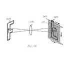
- Light from scene element 202is collected by optical system 204 in order to produce an optical image 206 on the face of the TDI image sensor.
- Scene element 202moves vertically upward with respect to optical system 204 and the TDI image sensor. This causes corresponding optical image 206 to move vertically downward across the surface of the TDI image sensor.
- the ICCDs of the TDI image sensorare clocked downward toward the RCCD of the TDI image sensor. As each line of accumulated packets of photocharge from the ICCDs is clocked vertically into the RCCD and then horizontally out through the TDI image sensor's charge-measurement and amplifier circuit, a line of pixels of the captured image is produced.
- horizontal clock line 108(see FIG. 1 ) may be used to block charge from the upper 15 / 16 of the ICCDs 102 , effectively reducing the integration time to 1/16 of the potential full integration time.
- horizontal clock line 110reduces integration time to 1 ⁇ 8 of the full integration time
- horizontal clock line 112reduces integration time to 1 ⁇ 4 of the full integration time
- horizontal clock line 114reduces integration time to 1 ⁇ 2 of the full integration time.
- a TDI image sensoris described in “A High Speed, Dual Output Channel, Stage Selectable, TDI CCD Image Sensor for High Resolution Applications” (Agwani, et al, Proc. SPIE, Vol. 2415, Page 124 (1995)).
- the device describedhas 2048 ICCDs, each ICCD consisting of 96 CCD integrating stages, and with the number of integrating stages selectable among 96, 48, 24, 12, and 6 stages.
- the RCCDis split into two CCDs, with one CCD for even-numbered ICCDs and the other for odd-numbered ICCDs, and with separate charge measurement and amplifier circuits associated with each of the two readout CCDs.
- the sensorprovides captured image pixel lines at up to 14,000 lines per second, and provides a dynamic range of 6000:1.
- TDI CCD image sensorsgenerally have very high sensitivity due to the long integration times provided by the ICCDs and also have flexibility in integration time by selecting the number of stages of integration employed, there remains a need for greater dynamic range.
- a natural body of water or water standing on the roof of a buildingmay reflect sunlight, while nearby scene elements may be dark or in shadow.
- the range of light level between the reflected sunlight and the dark areas of the scenemay far exceed the 6000:1 dynamic range of a typical CCD TDI image sensor such as the one described above.
- each ICCDis composed of 13 TDI stages, a conditional reset circuit, 4 more TDI stages, another conditional reset circuit, and a final TDI stage before reaching the RCCD.
- the conditional reset circuitsinclude a charge-measurement amplifier that controls a discharge gate: as each charge packet is clocked through the CCD stage associated with the conditional reset circuit, the amount of charge is measured. If the measured charge exceeds a threshold, the discharge gate is operated to remove the charge from the CCD.
- conditional reset circuitconsumes a significant amount of area, as it includes multiple transistors.
- a contactmust be placed in the CCD stage associated with the conditional reset circuit to permit the measurement of charge, and the contact has the potential for producing dark current or otherwise affecting the charge packet as it passes through the affected CCD stage.
- Embodiments of the present inventionincrease the dynamic range of TDI CCD image sensors by selectively controlling the projection of light onto the image sensor and/or selectively resetting one or more stages of one of more of the ICCDs of the image sensor while and/or prior to a scene being imaged by the TDI image sensor.
- the stagesare substantially identical to each other and are all independently resettable, in contrast to more complex conventional designs utilizing only a few specialized resettable stages.
- the dynamic-range control of the image sensormay be based on previously captured images, which may be captured either by the image sensor itself or another image sensor (termed a “leading sensor”) that is configured to capture light from a scene immediately prior to the scene being imaged by the TDI image sensor.
- Each of the ICCDsmay incorporate a sense node for measurement of charge within the ICCD channel and/or selective reset of stages of the ICCDs via direction of photocharge into the sense node.
- all of the ICCD stagesmay be configured for individual reset via application of a bias to the stage control line (each of which preferably controls a particular stage common across all of the ICCDs) and to a gate associated with each ICCD.
- a “scene”does not connote any particular content, and may be, e.g., a pictorial scene, a graphical scene (e.g., a document or other text), a medical image, etc.
- embodiments of the inventionfeature an imaging system that includes a time-delay-and-integrate (TDI) image sensor including or consisting essentially of (i) a plurality of integrating CCDs (ICCDs), arranged in parallel, that accumulate photocharge in response to exposure to light, (ii) electrically coupled to the plurality of ICCDs, a readout CCD (RCCD) for receiving photocharge from the plurality of ICCDs, and (iii) electrically coupled to the RCCD, readout circuitry for converting charge received from the RCCD into voltage.
- TTItime-delay-and-integrate
- An optical systemreceives light from a scene to be imaged and projects it on the plurality of ICCDs.
- a leading sensorreceives the light projected from the optical system prior to projection thereof on the plurality of ICCDs, thereby capturing a leading image of the scene.
- a control systemcontrols operation of the TDI image sensor based at least in part on at least a portion of the leading image.
- Embodiments of the inventionmay feature one or more of the following in any of a variety of combinations.
- the optical systemmay be configured to sweep the light from the scene across the leading sensor and the TDI image sensor continuously and sequentially.
- the leading sensormay be configured to collect color information related to the scene.
- the TDI image sensormay not be configured to collect color information related to the scene or may be configured to collect monochrome intensity levels (e.g., only monochrome intensity levels) related to the scene.
- the leading sensor and the TDI image sensormay be disposed on a substrate.
- the dynamic range of the leading sensormay be less than the dynamic range of the TDI image sensor.
- the control systemmay alter the integration time of at least one of the ICCDs based on the brightness level of at least a portion of the leading image.
- Each ICCDmay include or consist essentially of (i) a plurality of independently controllable stages, (ii) a photosensitive channel for containing photocharge, (iii) a drain for removing photocharge from the channel, and (iv) a gate for controlling flow of photocharge from the channel to the drain.
- a plurality of clock linesmay be disposed substantially perpendicular to the ICCDs. Each clock line may control a particular stage common to all of the ICCDs.
- the control systemmay be configured to reset a selected stage of a selected ICCD by (i) applying a bias to the clock line corresponding to the selected stage and (ii) applying a bias to the gate corresponding to the selected ICCD.
- Each ICCDmay include or consist essentially of (i) a plurality of independently controllable stages, (ii) a photosensitive channel for containing photocharge, (iii) a sense node for measuring photocharge received thereby from the channel, and (iv) a gate for controlling flow of photocharge from the channel to the sense node.
- the control systemmay be configured to (i) measure photocharge received by the sense node from the channel and (ii) reset the sense node by applying a bias thereto to remove photocharge therefrom.
- the control systemmay be configured to reset a selected stage of the ICCD by applying a bias to the gate to thereby allow photocharge to flow from the channel into the sense node.
- embodiments of the inventionfeature a method of image capture utilizing a time-delay-and-integrate (TDI) image sensor that includes or consists essentially of (i) a plurality of integrating CCDs (ICCDs), arranged in parallel, that accumulate photocharge in response to exposure to light, (ii) electrically coupled to the plurality of ICCDs, a readout CCD (RCCD) for receiving photocharge from the plurality of ICCDs, and (iii) electrically coupled to the RCCD, readout circuitry for converting charge received from the RCCD into voltage.
- a time-delay-and-integrate (TDI) image sensorthat includes or consists essentially of (i) a plurality of integrating CCDs (ICCDs), arranged in parallel, that accumulate photocharge in response to exposure to light, (ii) electrically coupled to the plurality of ICCDs, a readout CCD (RCCD) for receiving photocharge from the plurality of ICCDs, and (iii)
- Embodiments of the inventionmay feature one or more of the following in any of a variety of combinations.
- the projection of light onto the leading sensor and onto the plurality of ICCDsmay be performed continuously and sequentially.
- the leading imagemay include color information.
- the scene imagemay be substantially free of color information.
- Controlling operation of the TDI sensormay include or consist essentially of altering an integration time of at least one of the ICCDs based on the brightness level of at least a portion of the leading image.
- Controlling operation of the TDI sensormay include or consist essentially of masking portions of the ICCDs whereby light collection at such portions is attenuated.
- Controlling operation of the TDI sensormay include or consist essentially of resetting a selected stage of a selected ICCD.
- Resetting the selected stagemay include or consist essentially of transferring photocharge therewithin into a drain associated with the selected ICCD.
- Resetting the selected stagemay include or consist essentially of transferring photocharge therewithin into a sense node associated with the selected ICCD.
- the leading imagemay be compared with the scene image to detect motion in the scene.
- embodiments of the inventionfeature an imaging system including or consisting essentially of a time-delay-and-integrate (TDI) image sensor, an optical system for receiving light from a scene to be imaged, and an optical mask.
- the TDI image sensorincludes or consists essentially of (i) a plurality of integrating CCDs (ICCDs), arranged in parallel, that accumulate photocharge in response to exposure to light, (ii) electrically coupled to the plurality of ICCDs, a readout CCD (RCCD) for receiving photocharge from the plurality of ICCDs, and (iii) electrically coupled to the RCCD, readout circuitry for converting charge received from the RCCD into voltage.
- the optical systemprojects light from the scene to be imaged on the plurality of ICCDs.
- the optical maskis disposed between the optical system and the plurality of ICCDs and selectively alters the intensity of light projected to at least portions of the ICCDs.
- Embodiments of the inventionmay feature one or more of the following in any of a variety of combinations.
- the optical maskmay include or consist essentially of an array of independently controllable masking elements each for attenuating light collection by a different portion of the ICCDs.
- the optical maskmay include or consist essentially of an array of independently controllable reflective elements each for selectively reflecting a portion of the light from the optical system onto the ICCDs.
- a control systemmay control the optical mask based at least in part on light from the scene to be imaged before such light is projected by the optical system.
- embodiments of the inventionfeature a method of image capture utilizing a time-delay-and-integrate (TDI) image sensor comprising (i) a plurality of integrating CCDs (ICCDs), arranged in parallel, that accumulate photocharge in response to exposure to light, (ii) electrically coupled to the plurality of ICCDs, a readout CCD (RCCD) for receiving photocharge from the plurality of ICCDs, and (iii) electrically coupled to the RCCD, readout circuitry for converting charge received from the RCCD into voltage.
- TDItime-delay-and-integrate
- Embodiments of the inventionmay feature one or more of the following in any of a variety of combinations.
- the intensity of light projected to at least portions of the ICCDsmay be altered with an optical mask disposed between the scene and the ICCDs.
- the optical maskmay include or consist essentially of an array of masking elements each independently controllable to mask a portion of the ICCDs whereby light collection in the masked portion is attenuated.
- the optical maskmay include or consist essentially of an array of reflective elements each independently controllable to reflect a portion of the projected light onto the ICCDs.
- the selective alteration of the intensity of light projected to at least portions of the ICCDs during capture of the imagemay be based at least in part on a previously captured image.
- embodiments of the inventionfeature an imaging system including or consisting essentially of a time-delay-and-integrate (TDI) image sensor and an optical system for receiving light from a scene to be imaged.
- the TDI image sensorincludes or consists essentially of (i) a plurality of integrating CCDs (ICCDs), arranged in parallel, that accumulate photocharge in response to exposure to light, (ii) electrically coupled to the plurality of ICCDs, a readout CCD (RCCD) for receiving photocharge from the plurality of ICCDs, and (iii) electrically coupled to the RCCD, readout circuitry for converting charge received from the RCCD into voltage.
- ICCDsintegrating CCDs
- RCCDreadout CCD
- Each ICCDincludes or consists essentially of (i) a plurality of independently controllable stages, (ii) a photosensitive channel for containing photocharge, (iii) a drain for removing photocharge from the channel, and (iv) a gate for controlling flow of photocharge from the channel to the drain.
- Embodiments of the inventionmay feature one or more of the following in any of a variety of combinations.
- a plurality of clock linesmay be disposed substantially perpendicular to the ICCDs. Each clock line may control a particular stage common to all of the ICCDs.
- a control systemmay be configured to reset a selected stage of a selected ICCD by (i) applying a bias to the clock line corresponding to the selected stage and (ii) applying a bias to the gate corresponding to the selected ICCD.
- the control systemmay be configured to reset the selected stage based at least in part on a previously captured image (i.e., an image captured by the imaging system prior to the light from the scene to be imaged being projected by the optical system).
- embodiments of the inventionfeature a method of image capture utilizing a time-delay-and-integrate (TDI) image sensor comprising (i) a plurality of integrating CCDs (ICCDs), arranged in parallel and each comprising a plurality of stages, that accumulate photocharge in response to exposure to light, (ii) electrically coupled to the plurality of ICCDs, a readout CCD (RCCD) for receiving photocharge from the plurality of ICCDs, and (iii) electrically coupled to the RCCD, readout circuitry for converting charge received from the RCCD into voltage.
- TDItime-delay-and-integrate
- ICCDsintegrating CCDs
- RCCDreadout CCD
- Each stage of each ICCDis independently resettable.
- a selected stage of a selected ICCDis reset to remove photocharge from the selected stage. Resetting the selected stage may include or consist essentially of transferring photocharge therewithin into a drain associated with the selected ICCD.
- embodiments of the inventionfeature an imaging system including or consisting essentially of a time-delay-and-integrate (TDI) image sensor and an optical system for receiving light from a scene to be imaged.
- the TDI image sensorincludes or consists essentially of (i) a plurality of integrating CCDs (ICCDs), arranged in parallel, that accumulate photocharge in response to exposure to light, (ii) electrically coupled to the plurality of ICCDs, a readout CCD (RCCD) for receiving photocharge from the plurality of ICCDs, and (iii) electrically coupled to the RCCD, readout circuitry for converting charge received from the RCCD into voltage.
- ICCDsintegrating CCDs
- RCCDreadout CCD
- Each ICCDincludes or consists essentially of (i) a plurality of independently controllable stages, (ii) a photosensitive channel for containing photocharge, (iii) a sense node for measuring photocharge received thereby from the channel, and (iv) a gate for controlling flow of photocharge from the channel to the sense node.
- Embodiments of the inventionmay feature one or more of the following in any of a variety of combinations.
- a plurality of clock linesmay be disposed substantially perpendicular to the ICCDs. Each clock line may control a particular stage common to all of the ICCDs.
- a control systemmay be configured to (i) measure photocharge received by the sense node from the channel and (ii) reset the sense node by applying a bias thereto to remove photocharge therefrom.
- a control systemmay be configured to reset a selected stage of the ICCD by applying a bias to the gate to thereby allow photocharge to flow from the channel into the sense node.
- the control systemmay be configured to reset the selected stage based at least in part on a previously captured image (i.e., an image captured by the imaging system prior to the light from the scene to be imaged being projected by the optical system).
- embodiments of the inventionfeature a method of image capture utilizing a time-delay-and-integrate (TDI) image sensor comprising (i) a plurality of integrating CCDs (ICCDs), arranged in parallel, that accumulate photocharge in response to exposure to light, (ii) electrically coupled to the plurality of ICCDs, a readout CCD (RCCD) for receiving photocharge from the plurality of ICCDs, and (iii) electrically coupled to the RCCD, readout circuitry for converting charge received from the RCCD into voltage.
- TDItime-delay-and-integrate
- Each ICCDincludes or consists essentially of (i) a plurality of independently controllable stages, (ii) a photosensitive channel for containing photocharge, (iii) a sense node for measuring photocharge received thereby from the channel, and (iv) a gate for controlling flow of photocharge from the channel to the sense node. Light received from a scene to be imaged is projected onto the plurality of ICCDs.
- FIG. 1illustrates a conventional TDI CCD image sensor
- FIG. 2illustrates an exemplary operation mode of a TDI CCD image sensor
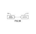
- FIG. 3Ais a block diagram of an image-capture device utilizing an image sensor in accordance with various embodiments of the invention.
- FIG. 3Bis a block diagram of portions of an image sensor in accordance with various embodiments of the invention.
- FIG. 4is a schematic plan view of portions of two ICCDs of a TDI CCD in accordance with various embodiments of the invention.
- FIG. 5is a schematic cross-section of a vertical portion of the ICCDs of FIG. 4 showing ICCD clock lines and associated potential diagrams in accordance with various embodiments of the invention
- FIG. 6is a schematic cross-section of a horizontal portion of the ICCDs of FIG. 4 showing two ICCD integrating channels with associated structures in accordance with various embodiments of the invention
- FIG. 7is a potential diagram for an unselected row of the ICCD stages of FIG. 6 in accordance with various embodiments of the invention.
- FIG. 8is a potential diagram for a selected row of the ICCD stages of FIG. 6 in accordance with various embodiments of the invention.
- FIG. 9expands the potential diagrams of FIG. 5 to depict four-phase clocking for multiple ICCD stages in accordance with various embodiments of the invention.
- FIG. 10expands the potential diagrams of FIG. 5 to depict four-phase clocking for multiple ICCD stages including two different rows selected for reset in accordance with various embodiments of the invention
- FIG. 11expands the potential diagrams of FIG. 10 to depict four-phase clocking for multiple ICCD stages including four different rows selected for reset in accordance with various embodiments of the invention
- FIG. 12is a potential diagram for an unselected row of the ICCD stages of FIG. 6 in accordance with various embodiments of the invention.
- FIG. 13is a potential diagram for an unselected row of the ICCD stages of FIG. 6 in accordance with various embodiments of the invention.
- FIG. 14is a modification of the potential diagrams of FIG. 11 depicting four-phase clocking for multiple ICCD stages including two different rows selected for reset in accordance with various embodiments of the invention
- FIG. 15is a potential diagram for individual gates of ICCD stages in accordance with various embodiments of the invention.
- FIG. 16is a schematic plan view of a portion of an ICCD of a TDI CCD in accordance with various embodiments of the invention.
- FIG. 17is a schematic cross section of a horizontal portion of the ICCD of FIG. 16 depicting an ICCD integrating channel with associated structures in accordance with various embodiments of the invention
- FIG. 18is a potential diagram for an unselected gate of the ICCD of FIG. 17 in accordance with various embodiments of the invention.
- FIG. 19is a potential diagram depicting charge spillover for an unselected gate of the ICCD of FIG. 17 in accordance with various embodiments of the invention.
- FIG. 20is a potential diagram depicting charge discharge for a selected gate of the ICCD of FIG. 17 in accordance with various embodiments of the invention.
- FIG. 21is a potential diagram depicting an unselected gate and no charge in an ICCD integrating channel of the ICCD of FIG. 17 in accordance with various embodiments of the invention.
- FIG. 22is a circuit diagram of a spillover charge-measurement circuit in accordance with various embodiments of the invention.
- FIG. 23is a schematic cross-section of a system in which a travelling optical mask is in virtual contact with a sensor in accordance with various embodiments of the invention.
- FIG. 24is a schematic cross-section of a system in which an image passing through a travelling optical mask is relayed to a sensor in accordance with various embodiments of the invention.
- FIG. 25is a schematic cross-section of a system in which an image reflected from a travelling optical mask is relayed to a sensor in accordance with various embodiments of the invention.
- FIG. 26illustrates an exemplary operation mode of a TDI sensor with a leading sensor in accordance with various embodiments of the invention.
- FIG. 3Ais a block diagram of an exemplary image-capture device 300 that includes an electronic image sensor 304 in accordance with various embodiments of the invention.
- incoming light 302 from a scene to be capturedis focused on image sensor 304 by optical system 204 .
- Image sensor 304provides an analog electronic signal that is representative of the optical image focused on the image sensor.
- This analog signalis processed by an analog signal processor 306 .
- the analog signal processor 306typically performs one or more of the functions of signal sampling, reference/signal correlation, gain, black-level adjustment, and other analog processing.
- the output of the analog signal processor 306is converted to digital output 310 by analog-to-digital (A/D) converter 308 .
- A/Danalog-to-digital
- a timing generatorsynchronizes the operation of the image sensor 304 , the analog signal processor 306 , and the A/D converter 308 .
- Two or more elements of image-capture device 300may be combined into a single device: for example, the analog signal processor 304 , the A/D converter 308 , and the timing generator 312 may be combined into a single integrated circuit.
- an element of image-capture device 300may be composed of multiple devices: for example, the timing generator 312 may be composed of an integrated circuit that provides logic-level timing signals and other integrated circuits and/or support circuitry that convert some of the logic-level timing signals into signals appropriate for driving the image sensor.
- the image sensor 304may be an areal-array sensor, a linear-array sensor, a TDI sensor, or other electronic image sensor.
- the image sensor 304typically employs CCD technology, active pixel sensor (i.e., CMOS image sensor) technology, or other image-sensor technology.
- the TDI CCD image sensor 100includes multiple ICCDs 102 , RCCD 104 , and charge-measurement and amplifier circuit 106 .
- embodiments of the present inventionemploy similar structures.
- various embodiments of the present inventionprovide improvements to the structure and operation of the ICCDs 102 .
- the ICCD 102is considered to be a charge-coupled device because it enables packets of charge to be maintained separately from each other and also enables the packets of charge to be shifted along the length of the ICCD.
- the ICCD 102is also considered to be an integrating device because photon-induced charge (photocharge) increases the amount of charge in a charge packet during the period of time the charge packet remains in the ICCD. By collecting photocharge into packets of charge during the time the packets are shifted along its length, the ICCD 102 permits significantly increased integration time and consequently significantly increased sensitivity.
- FIG. 3Bschematically depicts image sensor 304 linked to a controller (or “control system”) 314 that controls various operations of image sensor 304 , including image capture and read out (and other functionality described below), as well as various operations of other components of image-capture systems described herein.
- controlleror “control system”
- the controller 314(which in various embodiments of the invention includes or performs the functionalities of the analog signal processor 306 , the A/D converter 308 , and the timing generator 312 ) may be a general-purpose microprocessor, but depending on implementation may alternatively be a microcontroller, peripheral integrated circuit element, a customer-specific integrated circuit (CSIC), an application-specific integrated circuit (ASIC), a logic circuit, a digital signal processor, a programmable logic device such as a field-programmable gate array (FPGA), a programmable logic device (PLD), a programmable logic array (PLA), an RFID processor, smart chip, or any other device or arrangement of devices that is capable of implementing the steps of the processes of the invention (such as those described in detail below).
- CSICcustomer-specific integrated circuit
- ASICapplication-specific integrated circuit
- FPGAfield-programmable gate array
- PLDprogrammable logic device
- PLAprogrammable logic array
- RFID processorsmart chip, or any other device or arrangement of devices that is capable of
- the controller 314may be monolithically integrated with, and thus a portion of the same integrated-circuit chip as, image sensor 304 , or controller 314 may be disposed on a chip separate and discrete from the chip containing image sensor 304 (and interconnected thereto by wired or wireless means). Moreover, at least some of the functions of controller 314 may be implemented in software and/or as mixed hardware-software modules. Software programs implementing the functionality herein described may be written in any of a number of high level languages such as FORTRAN, PASCAL, JAVA, C, C++, C#, BASIC, various scripting languages, and/or HTML. Additionally, the software may be implemented in an assembly language directed to a microprocessor resident in controller 314 .
- the softwaremay be embodied on an article of manufacture including, but not limited to, a floppy disk, a jump drive, a hard disk, an optical disk, a magnetic tape, a PROM, an EPROM, EEPROM, field-programmable gate array, CDROM, or DVDROM.
- Embodiments using hardware-software modulesmay be implemented using, for example, one or more FPGA, CPLD, or ASIC processors.
- FIG. 4A plan view of portions of two adjacent ICCDs 400 of a TDI CCD in an embodiment of the present invention is shown in FIG. 4 .
- FIG. 5includes a cross-section of a vertical portion of one of the ICCDs 400 , as shown by the cut line 5 - 5 in FIG. 4 .
- FIG. 6is a cross-section that cuts horizontally through both of the ICCDs 400 , as shown by cut line 6 - 6 in FIG. 4 .
- FIG. 5depicts one stage of an ICCD 400 in accordance with an embodiment of the present invention.
- Four ICCD clock linesare shown: ICCD clock line 1 ( 502 ), ICCD clock line 2 ( 504 ), ICCD clock line 3 ( 506 ), and ICCD clock line 4 ( 508 ). Voltages are applied sequentially to these ICCD clock lines in order to produce potential gradients in the underlying semiconductor, during which packets of charge are kept separate and are moved along the length of the ICCD 400 .
- the four clock lines 502 , 504 , 506 , 508are operated in four phases to hold and move charge in a manner well understood by those skilled in the art of CCD design and operation.
- the potential diagrams ⁇ 1 , ⁇ 2 , ⁇ 3 , and ⁇ 4illustrate the potentials developed under each of the four ICCD clock lines for each of the four phases used in normal operation of ICCD 400 .
- a charge packet 510is held under ICCD clock line 1 ( 502 ) and ICCD clock line 2 ( 504 ), and the charge packet is separated from other charge packets by ICCD clock line 3 ( 506 ) and ICCD clock line 4 ( 508 ).
- This arrangement of ICCD clock lines and potentialsis repeated over the length of the ICCD 400 so that, for example, the ICCD clock line immediately to the left of ICCD clock line 1 is electrically connected to and driven to the same voltage as ICCD clock line 4 , thereby acting to contain the charge packet 510 on its left side.
- the charge packet 510 in a typical CCDis composed of electrons, so a more positive voltage potential produces an area for electrons to collect.
- ICCD clock lines 1 ( 502 ) and 2 ( 504 )produce a storage region for holding a charge packet
- ICCD clock lines 3 ( 506 ) and 4 ( 508 )produce a barrier region for separating charge packets.
- potential diagram ⁇ 2the charge packet is moved to the right (or vertically downward with respect to FIG. 4 ) by changing the voltages on ICCD clock lines 1 ( 502 ) and 3 ( 506 ).
- potential diagrams ⁇ 3 and ⁇ 4move the charge packet two more clock lines to the right.
- potential diagrams ⁇ 1 through ⁇ 4are referred to alternatively as phase ⁇ 1 through ⁇ 4 .
- the four ICCD clock lines 502 , 504 , 506 , 508together constitute one stage of an ICCD 400 .
- the arrangement in FIG. 5is repeated to produce a complete ICCD 400 that has, for example, 32, 48, 64, or 96 stages.
- a charge packet moving along the ICCD 400 and accumulating photocharge along the wayis an “integrating pixel;” when an integrating pixel is read out from the ICCD 400 it becomes a pixel of the capture image.
- FIG. 5includes a potential diagram ⁇ 2 ′ that is an alternative to potential diagram ⁇ 2 .
- potential diagram ⁇ 2 ′the voltages applied to the ICCD clock lines 502 , 504 , 506 , 508 are adjusted to shift the barrier and storage regions of the corresponding ICCD stage with respect to adjacent stages. This shifting is shown by the arrows in potential diagram ⁇ 2 ′.
- the shiftingoccurs in common for the corresponding stage in all the ICCDs 400 of the TDI image sensor: in reference to FIG. 1 , this defines a horizontal row of ICCD stages, one stage from each ICCD 102 in FIG. 1 .
- the cross-section in FIG. 6cuts along one ICCD clock line 602 and across two ICCDs 400 constructed in accordance with an embodiment of the invention. Specifically, the cross-section in FIG. 6 cuts along ICCD clock line 2 ( 504 in FIG. 5 ).
- Channel stop implants 604 in FIG. 6produce potential barriers to separate each ICCD 400 from adjacent ICCDs 400 .
- Drain implants 606produce potential regions that permit removal of charge from the adjacent ICCD 400 .
- Gates 608produce potential regions that provide a barrier between an ICCD 400 and its corresponding drain implant 606 ; the gates 608 are individually externally controllable to eliminate the barrier between an ICCD 400 and its corresponding drain implant 606 , thereby allowing charge to flow from the ICCD 400 into the drain implant 606 under certain conditions.
- FIG. 7is a potential diagram associated with FIG. 6 for an unselected row of an ICCD in accordance with an embodiment of the invention.
- the ICCD clock linesare driven to produce the potentials associated with potential diagram ⁇ 2 in FIG. 5 .
- the gate 608 associated with the left ICCDremains in a state that produces a barrier between the left ICCD and its corresponding drain 606 (left 606 in FIG. 6 ), thereby preventing the charge packet 702 within the integrating pixel thus defined from flowing into the drain 606 .
- the gate 608 associated with the right ICCD(right 608 in FIG.
- potential diagram ⁇ 2 in FIG. 5prevents an integrating pixel from being reset (the charge packet being drained away) regardless of the states of the gates associated with the ICCDs.
- potential diagram ⁇ 2 in FIG. 5represents an unselected row of ICCD stages that may prevent integrating pixels from being reset regardless of whether an ICCD is selected (e.g., the right ICCD in FIG. 7 ) or unselected (e.g., the left ICCD in FIG. 7 ).
- FIG. 8is a potential diagram associated with FIG. 6 for a selected ICCD row in accordance with an embodiment of the invention.
- the ICCD clock linesare thus driven to produce the potentials associated with potential diagram ⁇ 2 ′ in FIG. 5 .
- the barrier produced by the gate 608 associated with the left ICCD(left 608 in FIG. 6 ) is sufficient to prevent the charge packet 802 from flowing into the drain 606 .
- the charge packet 802is effectively held by a storage region defined by the potentials associated with ICCD clock lines 1 and 4 ( 502 and 508 in FIG. 5 ), the gate 608 associated with the left ICCD (left 608 in FIG.
- the channel stop implant 604 associated with the left ICCD(leftmost 604 in FIG. 6 ).
- the reduced barrier produced by the gate 608 associated with the right ICCD(right 608 in FIG. 6 ) is now lower than the floor of the storage region in the right ICCD, thereby allowing the charge packet 804 to flow into the corresponding drain 606 .
- the concurrent selection of a row of ICCD stages along with a selected ICCDwill cause the integrating pixel from the corresponding storage region to be reset (i.e., the charge packet confined therein to flow to the drain). This effectively reduces the available integration time for the integrating pixel, after being reset, to be the time spent in the remaining ICCD stages between where the integrating pixel reset occurred and the end of the ICCD.
- any integrating pixelmay be reset at any point as it is clocked along its corresponding ICCD by selection of the appropriate ICCD clock lines (thereby selecting a row of ICCD stages) and ICCD gate (thereby selecting a particular ICCD).
- the selective reset of integrating pixelsprovided by this arrangement enables integrating pixels associated with bright regions of the scene to be reset at a point close to the end of the ICCD, thereby permitting them to have a short effective integration time.
- integrating pixels associated with middle ranges of scene brightnessare enabled to be reset in the middle of the ICCD, permitting them to have a medium length effective integration time. Integrating pixels associated with dark areas of the scene may not be reset at all, permitting them to have the maximum integration time enabled by all stages of the ICCD. This has the effect of significantly increasing the dynamic range of the TDI image sensor in accordance with embodiments of the present invention.
- the embodiments of the invention described aboveprovide the advantage of increased dynamic range without the shortcomings of earlier approaches.
- the drain and gate structures associated with each ICCDare compact structures. All of the ICCD stages are typically identical in the disclosed embodiment, and thus no specialized stages incorporating charge-measurement and discharge circuitry are required. Embodiments of the present invention also do not require a contact to be placed in the ICCD for charge measurement, thereby eliminating a potential source of dark current or other undesirable effects.
- the controller that controls these elements and thereby causes the reset of integrating pixelshas knowledge of which integrating pixels were reset and at which ICCD stage they were reset. Consequently, in contrast to the output pixels produced by conventional sensors, there is no ambiguity regarding the output pixels: since the reset conditions for a particular integrating pixel are known, the integration time for the corresponding output pixel is also known.
- “Externally controllable,” as used in the foregoing discussion,means that the determination regarding which integrating pixels to reset and at which ICCD stage to reset them occurs separately from the ICCDs and in such a way that the knowledge of which integrating pixels were reset and at which stage they were reset is available for subsequent image-processing purposes.
- Externally controllableis not necessarily equivalent to “directly controlled,” as there may be intervening circuitry such as decoders, control registers, shift registers, or the like between the controller that resets the integrating pixel and the ICCD clock lines and gates.
- Externally controllablemeans external to the array of ICCDs and does not imply that control elements must be on a separate integrated circuit substrate; all or a portion of the elements of the external control may be integrated into the same integrated circuit substrate as the ICCDs, they may be incorporated into an integrated circuit substrate that has been bonded to the TDI sensor, or they may be separate.
- n16
- Integrating pixels that are not reset at any of the sixteen stageshave sixteen stages of integration.
- the selective reset of integrating pixelsincreases the dynamic range of the image sensor by a factor of 16. This arrangement has the additional benefit of restricting to four stages the different clocking utilized to select a row of ICCD stages for possible integrating-pixel reset. This is discussed in more detail below.
- FIG. 9expands the potential diagrams from FIG. 5 to depict four-phase clocking for five ICCD stages.
- operating the ICCD clock lines to produce the potentials shown in potential diagrams ⁇ 1 through ⁇ 4 (and back again to potential diagram ⁇ 1 )moves a charge packet exactly one stage to the right.
- Each cycle through potential diagrams ⁇ 1 through ⁇ 4 in FIG. 9moves charge packets one stage to the right.
- the ICCD potential profiles related to the potential diagrams ⁇ 1 through ⁇ 4 in FIG. 9 and subsequent figuresare also referred to as phases ⁇ 1 through ⁇ 4 .
- FIG. 9shows the same five ICCD stages and similar phase clocking as in FIG. 9 , but phase ⁇ 2 is modified in the same manner as in FIG. 5 in order to select integrating pixels one stage from the right for possible reset and phase ⁇ 1 is modified in order to select integrating pixels approximately two stages from the right for possible reset.
- the rightmost stage of FIGS. 9 , 10 , and 11is assumed to be in communication with the RCCD and that the integrating pixel is read out of the rightmost stage into the RCCD during phase ⁇ 3 .
- selected integrating pixelsare reset one stage from the right and are subsequently permitted to integrate only during the subsequent sequence of four phases ⁇ 3 , ⁇ 4 , ⁇ 1 , and ⁇ 2 required to transport the integrating pixels through the rightmost ICCD stage.
- selected integrating pixelsare reset approximately two stages from the right and are subsequently permitted to integrate only during the subsequent nine phases required to transport the integrating pixels through the rightmost two ICCD stages.
- the ICCD clock lines associated with the selected stageare controlled independently from the other clock lines to permit different voltage levels to be applied to them.
- ICCD clock lines 1 A, 2 A, 3 A, and 4 A for the second stage from the rightare independent (i.e., independently controllable) from the other ICCD clock lines to permit the second stage from the right to be selected.
- ICCD clock line 4 B for the fourth stage from the right and clock lines 1 B, 2 B, and 3 B for the third stage from the rightare independent from the other ICCD clock lines.
- ICCD clock lines 1 , 2 , 3 , and 4are typically connected together by wiring at the edges of the array of ICCDs in a TDI CCD sensor and are consequently controlled in common for all stages, but the ICCD clock lines 1 A, 2 A, 3 A, 4 A, 4 B, 1 B, 2 B, and 3 B herein are capable of being controlled independently of ICCD clock lines 1 , 2 , 3 , and 4 .
- phases ⁇ 1 and ⁇ 2select two different points in the ICCDs at which integrating pixels are permitted to be selectively reset.
- Phases ⁇ 3 and ⁇ 4are similarly modified to select yet another two different points in the ICCDs for selectively resetting integrating pixels.
- FIG. 11expands FIG. 10 to show 11 ICCD stages and includes modifications to phases ⁇ 3 and ⁇ 4 that permit integrating pixels to be selectively reset at another two points in the ICCDs.
- phase ⁇ 2permits integrating pixels to be selectively reset one ICCD stage (four phases) before readout (at label A); phase ⁇ 1 permits integrating pixels to be selectively reset two and one-quarter ICCD stages (nine phases) before readout (at label B); phase ⁇ 4 permits integrating pixels to be selectively reset four and one-half ICCD stages (eighteen phases) before readout (at label C); and phase ⁇ 3 permits integrating pixels to be selectively reset eight and three-quarters ICCD stages (thirty-five phases) before readout (at label D). Assuming the ICCDs in FIG. 11 include 16 stages in total, each integrating pixel delivered to the RCCD integrates light over time selected from four phases, nine phases, eighteen phases, thirty-five phases, or sixty-four phases.
- the storage regions produced by the ICCD clock lines, barrier implants, and gateshave a limited capacity for holding electrical charge. If the charge capacity of a storage region is exceeded by an integrating pixel's charge packet, the excess charge may spill into adjacent ICCDs or adjacent storage regions, thereby corrupting nearby integrating pixels. This spillover process is typically called “blooming.” This is a particular problem for those integrating pixels associated with the brightest regions of the scene. For example, if a particular integrating pixel is selected for reset one ICCD stage before being read out of the ICCD, this means that it requires only one stage of integration to reach a reasonable signal level for measurement. If there are sixteen stages in the complete ICCD, this particular integrating pixel has probably exceeded the charge capacity of the storage regions after integrating for only a few stages. As it continues to collect charge after that point, the integrating pixel may cause blooming.
- integrating pixels selected for reset at a particular ICCD stageare also reset at every earlier opportunity.
- an integrating pixelis selected for reset during phase ⁇ 2 four phases before readout, it is also reset during phase ⁇ 1 nine phases before readout, phase ⁇ 4 eighteen phases before readout, and phase ⁇ 4 thirty-five phases before readout.
- FIG. 12has the same potential profile as FIG. 7 showing the potential profile for an unselected row and an unselected ICCD gate (left ICCD) and a selected ICCD gate (right ICCD).
- charge packet 1202 in the left ICCDis confined like charge packet 702 in FIG. 7
- charge packet 1204 in the right ICCDexceeds the charge capacity of the storage region. Instead of blooming into neighboring storage regions, the excess charge flows into the drain.
- the ICCD gatesare used selectively for blooming control in an embodiment in accordance with the invention.
- the ICCD gatesare driven to a voltage to permit excess charge to be drained from the integrating pixels.
- FIG. 13is a modification of FIG. 7 that shows an unselected row with both ICCD gates operated to lower the barriers between the ICCDs and their associated drains.
- Charge packet 1302 in the left ICCDdoes not exceed the storage region's charge capacity.
- Charge packet 1304 in the right ICCDexceeds the storage region's charge capacity, but the excess charge flows harmlessly into the associated drain.
- the ICCD gateswhen used specifically for blooming control, they need not be driven to the same voltage as when they are used for selective reset of integrating pixels.
- This use of the ICCD gates for blooming controlis analogous to a lateral overflow drain (LOD) for excess charge.
- LODlateral overflow drain
- each phase ⁇ 1 through ⁇ 4is split into two parts, one part in which a row of ICCD stages is selected for possible integrating pixel reset and another part in which the row of ICCD stages is deselected and during which the ICCD gates are driven to a voltage appropriate for blooming control.
- one or more of the phases ⁇ 1 through ⁇ 4is used to provide an opportunity for blooming control.
- phases ⁇ 1 and ⁇ 3each select a row of ICCD stages for possible reset of integrating pixels, while no ICCD stages are selected for reset in phases ⁇ 2 and ⁇ 4 .
- the ICCD gatesare driven to a voltage appropriate for blooming control as shown in FIG. 13 .
- two modes of operationare enabled.
- the ICCD clock lines and gatesare operated to provide selective reset of integrating pixels and, optionally, blooming control.
- the ICCD clock linesare operated only to permit charge transfer along the ICCD; no rows of ICCD stages are selected for possible reset of integrating pixels.
- the ICCD gatesoptionally are operated in order to enable an LOD for blooming protection.
- This second mode of operationis useful when the scene to be captured has a low light level and a limited dynamic range, so that all integrating pixels are integrated over the full length of the ICCDs and none are reset. In this case, the charge capacity of the storage regions in the ICCDs is increased by maintaining the voltage of the ICCD gates such that the potential barrier produced by the gate is greater than the barrier produced when the gate is used for selecting an integrating pixel for reset.
- the ICCD gatesare separated into individual gates that are associated with individual ICCD stages or with individual ICCD clock lines within the individual stages. Control of the gates is provided by circuitry on another integrated circuit that is connected to the gates by wafer-to-wafer or die-to-die bonding. For example, individual ICCD gates are associated with the ICCD clock lines 2 and 3 in FIG. 5 in each stage of each ICCD. During phase ⁇ 2 in FIG. 5 , charge packets associated with integrating pixels selected for reset are allowed to flow into the drain associated with the ICCD by operating the corresponding individual gates. Since control of the gates is provided by separate circuitry, the gates may be controlled independently and there is no need for selecting a row of ICCD stages for possible reset of integrating pixels.
- FIG. 15shows the operation of individual gates for each ICCD as described in the previous paragraph.
- FIG. 15is similar to FIG. 8 in that it shows the potential profile across two ICCDs along clock line 2 , but clock line 2 is in its conventional storage state, not in a state to select a row of ICCD stages.
- the individual gate associated with the right ICCDis operated to allow the charge packet 1504 associated with integrating pixel in the right ICCD to flow into the drain.
- the individual gate associated with the left ICCDis set to a point that provides blooming protection, so that excess charge in the charge packet 1502 is allowed to flow into the drain instead of blooming.
- Providing individual gates for the ICCD stagesallows increased flexibility in operation. For example, for integrating pixels that are selected to be reset in order to reduce their integration time, those integrating pixels are reset repeatedly as they pass through each stage of the ICCD.
- FIG. 16is a plan view of portions of ICCDs of a TDI CCD in another embodiment of the present invention.
- ICCD clock line 1 ( 502 ), ICCD clock line 2 ( 504 ), ICCD clock line 3 ( 506 ) and ICCD clock line 4 ( 508 )are oriented horizontally in FIG. 16 , which also depicts channel stops 1602 and 1604 .
- a sense node 1606e.g., a floating diffusion node electrically isolated from other nodes in the device and where received photocharge may be converted to a voltage
- channel stop 1602 and channel stop 1604is located between channel stop 1602 and channel stop 1604 .
- FIG. 17cuts along ICCD clock line 2 ( 504 ) across an ICCD constructed in accordance with an embodiment of the present invention.
- Channel stop implants 1604 in FIG. 17produce potential barriers to separate each ICCD from adjacent ICCDs.
- Sense node implant 1606provides a region that is resettable to permit the collection and measurement of spillover charge from the ICCD integrating channel as will be described below in more detail.
- Gate 1610produces a potential region that provides an adjustable barrier between an ICCD integrating channel and its corresponding sense node implant 1606 .
- FIGS. 18-21are potential diagrams associated with FIG. 17 for an ICCD in accordance with an embodiment of the invention.
- the ICCD clock linesare driven to produce the potentials associated with potential diagram ⁇ 2 in FIG. 5 so that a storage region to hold a charge packet associated with an integrating pixel is in the ICCD integrating channel adjacent to gate 1610 .
- FIG. 18the gate 1610 is held in a state that holds integrating pixel charge packet 1802 in the integrating channel of the ICCD.
- the sense node 1606 adjacent to gate 1610has been reset by momentarily connecting it to ground in order set the sense node potential to a known state.
- FIG. 18also depicts a charge packet 1804 in a neighboring storage region.
- the charge packet 1802is held by the storage region potential profiles produced by the left channel stop 1604 , ICCD clock line 1 ( 502 ), ICCD clock line 4 ( 508 ), channel stop 1602 , and gate 1610 .
- the storage region produced by these elementshas a limited capacity for holding electrical charge.
- the charge packet 1802is less than the charge capacity of the storage region.
- the charge packet 1902 in FIG. 19exceeds the charge capacity of the storage region.
- the excess charge from charge packet 1902is allowed by the potential produced by the gate 1610 to spill into the sense node 1606 , as shown in FIG. 19 (as shown, neighboring charge packet 1904 is unaffected by such a spill over).
- spikeover chargeCharge that spills into the sense node 1606 is termed “spillover charge.”
- the potential produced by the charge in sense node 1606may be measured by a measurement circuit, or the sense node 1606 may be reset in order to remove the spillover charge, or both actions may be done in sequence in embodiments of the present invention.
- the gate 1610is operated to eliminate the barrier between the storage region and the sense node 1606 , allowing the charge 2002 in the storage region to flow into the sense node 1606 (again with no impact on neighboring charge packet 2004 ). This permits integration to be restarted for the integrating pixel in the integrating channel of the ICCD. If the sense node has sufficient charge capacity it is capable of holding all of the charge from the storage region. Alternatively, the charge is removed by resetting the sense node.
- any integrating pixel being clocked along an ICCDmay be reset at any ICCD stage by the operation of the gate and sense node as described with respect to FIGS. 18-21 .
- the selective reset of integrating pixelsprovided by this arrangement enables integrating pixels associated with bright regions of the scene to be reset at a point close to the end of the ICCD, thereby permitting them to have a short effective integration time.
- integrating pixels associated with middle ranges of scene brightnessare enabled to be reset in the middle of the ICCD, permitting them to have a medium length effective integration time. Integrating pixels associated with dark areas of the scene do not have to be reset at all, permitting them to have the maximum integration time allowed by all stages of the ICCD. This has the effect of significantly increasing the dynamic range of the TDI image sensor.
- the gate and sense node associated with an ICCD stageare compact structures. All of the ICCD stages are identical in the disclosed embodiment, unlike the conventional stages that incorporate specialized charge measurement and discharge circuitry. Embodiments of the present invention also do not require the placement of a contact in the ICCD for charge measurement, thereby eliminating the possibility of disrupting the integrating pixel with dark current or other undesirable effects.
- the gate and sense nodeare externally controllable, the entity that controls these elements and thereby causes the reset of integrating pixels has knowledge of which integrating pixels were reset and at which ICCD stage they were reset. Consequently, in contrast to the output pixels produced by conventional sensors, there is no ambiguity regarding the output pixels: since the reset conditions for a given integrating pixel are known, the integration time for the corresponding output pixel is also known.
- the storage regions produced by the ICCD clock lines, barrier implants, and gateshave a limited capacity for holding electrical charge. If the charge capacity of a storage region is exceeded by an integrating pixel's charge packet, the excess charge may spill into adjacent ICCDs or adjacent storage regions, thereby corrupting nearby integrating pixels (which, as detailed above, is typically referred to as “blooming”). This is a particular problem for those integrating pixels associated with the brightest regions of the scene. For example, if a particular integrating pixel is selected for reset one ICCD stage before being read out of the ICCD, this means that it requires only one stage of integration to reach a reasonable signal level for measurement. If there are sixteen stages in the complete ICCD, this particular integrating pixel has probably exceeded the charge capacity of the storage regions after integrating for only a few stages. As it continues to collect charge after that point, the integrating pixel may cause blooming.
- integrating pixels selected for reset at a particular ICCD stagemay be reset at every earlier opportunity, as also described above.
- the gateis used selectively for blooming control in an embodiment in accordance with the invention.
- the gateis set to a level that sets a threshold for charge that is lower than the other storage region barriers, causing excess charge to spill preferentially over the gate barrier into the sense node. This use of the gate for blooming control produces a lateral overflow drain for excess charge.
- the threshold for spillover chargeis adjustable depending on the voltage applied to the gate.
- the discussion to this pointrelates to using the gate and sense node for resetting an integrating pixel or for providing blooming protection.
- the gate and sense nodealso provide a way to measure the spillover charge. This measurement is used to make decisions regarding which integrating pixels to reset and at which ICCD stage to set them. Alternatively, the spillover charge measurements are used to augment the measured integrating pixels.
- FIG. 22shows a spillover charge measurement circuit 2200 in accordance with an embodiment of the invention.
- Sense node 1606is electrically connected to reset and readout circuitry by a conductor 2202 .
- the voltage of gate 1610is controlled by a conductor 2204 and a terminal 2206 .
- the sense node 1606is connected to a source follower 2208 .
- a reset gate 2210is operated by a terminal 2212 in order to connect the sense node 1606 to ground to establish a known reset state for the sense node 1606 .
- Sense node 1606converts spillover charge into a voltage, a process that depends on the capacitance of the sense node 1606 : a small capacitance produces a higher voltage than a large capacitance for the same amount of charge.
- reset and reset samplemay occur during phase ⁇ 4 when the gate is adjacent to a barrier region and signal sample may occur during subsequent phase ⁇ 2 when the gate is adjacent to a storage region.
- a measurementmay also be done with only the signal sample, although the result may have somewhat higher error.
- the capacitance of the sense node 1606may be made very small so small amounts of spillover charge cause large voltage swings at the sense node 1606 ; this effectively provides a high gain measurement of the spillover charge.
- the measured spillover chargeis used for any of several purposes in embodiments in accordance with the invention.
- the charge spillover measurements associated with the passage of an integrating pixel along the ICCDmay be stored and used along with the measured integrating pixel to determine a final extended dynamic range pixel. Integrating pixels associated with dark areas of a scene to be captured will typically have no spillover charge, so the spillover charge measurements will be zero and the measured integrating pixel alone provides the result. Integrating pixels associated with bright areas of the scene may have significant amounts of spillover charge beginning soon after the integrating pixels begin travelling along the ICCD. The combination of the spillover charge measurements for a brightly illuminated integrating pixel and the measurement of the integrating pixel itself provides the final pixel value.
- Integrating pixels associated with mid-range brightness areas of the scenewill typically have modest amounts of charge spillover that begins after some number of ICCD stages have been passed by the integrating pixels.
- the non-zero spillover charge measurements for a mid-range illuminated integrating pixel and the measurement of the integrating pixel itselfprovides the final pixel value.
- a thresholdmay be applied to the spillover charge measurements to determine whether or not a particular measurement should be used.
- the spillover charge measurementmay also be utilized to determine which integrating pixels to reset and at which stage of the ICCD to reset them. For example, if spillover charge is detected after an integrating pixel has traversed the first two stages of an ICCD, then the light level for that integrating pixel is such that the integrating pixel requires only a single stage of integration. Consequently, the integrating pixel is reset through every subsequent stage of the ICCD until it reaches the final stage, at which point it is allowed to integrate through the final stage.
- any integrating pixels that do not cause charge spillover of that lower gate thresholdcan integrate for the full 16 stages without causing charge spillover. If charge spillover occurs, the measured charge spillover is used to determine how many stages of integration are required, provided the charge spillover does not saturate the sense node 1606 . If the charge spillover saturates the sense node, then the next stage of the ICCD has its gate adjusted to allow spillover at a higher amount of charge, thereby refining the measurement of spillover charge for those integrating pixels that saturated the measurement at the first stage.
- gate thresholds and detecting and measuring spillover chargemay be used in a successive-approximation fashion to determine the number of final stages through which each integrating pixel should be run, resetting the integrating pixel up until that point. Variations in gate thresholds due to manufacturing or other variations may require calibration or application of calculation thresholds when using the spillover charge measurements in determining a final pixel value or when used for spillover charge detection.
- the transistors and reference levels described abovehave been NMOS transistors and reference levels suitable for operation with an electron-collecting CCD arrangement, PMOS transistors and corresponding reference levels may be used with a hole-collecting CCD arrangement.
- each pixel of the earlier captured imagemay correspond to several integrating pixels in the TDI capture, with the determination of integrating pixel reset being made collectively for small clusters of integrating pixels or being made on the basis of an interpolation of the pixels of the earlier captured image.
- FIG. 23illustrates yet another embodiment in accordance with the invention in which the dynamic range of the TDI CCD sensor is enhanced via the selective blocking of portions of the scene to be imaged (preferably bright areas of the scene).
- light from a scene element 2302is collected by an optical system 2304 in order to produce an optical image on the face of a transmissive optical mask array 2306 .
- the optical mask array 2306may be either in contact with or in very close proximity to a TDI image sensor 2308 .
- the optical mask array 2306may be an array of switchable optical elements, each of which may be switched between an optically transmitting state and a partially or completely optically blocking state.
- the optical imagemoves with respect to the TDI image sensor 2308 and the optical mask array 2306 , and the TDI image sensor 2308 is clocked concurrently with the movement of the optical image.
- the switchable optical elements of the optical mask array 2306are switched in order to match the motion of the optical image and the clocking of the TDI image sensor 2308 .
- the optically attenuating or blocking mask 2306may be utilized to track a bright area of the scene, thereby preventing at least a portion of the bright light from reaching the TDI image sensor 2308 .
- the light from a bright area of the scenemay be controlled by using the switchable optical elements of optical mask array 2306 to provide a synchronously travelling optical mask that blocks light from reaching the TDI image sensor 2308 for part of the time that the corresponding integrating pixels in the TDI image sensor 2308 are being clocked through the ICCDs of the TDI image sensor 2308 .
- Knowledge of which pixels in the image captured by the TDI image sensor were affected by the optical maskis combined with the pixels of the captured image in order to provide an extended dynamic range image.
- the optical mask array 2306is partially attenuating for the full time that corresponding integrating pixels travel along the ICCDs of the TDI image sensor, fully attenuating for part of the travel time, or a combination of partially attenuating and fully attenuating for the travel time.
- the optical mask array 2306 in FIG. 23may be fabricated in any of several different ways.
- the optical mask array 2306is made by employing liquid crystal technology.
- the liquid crystal materialin conjunction with optical polarizers and X-Y addressing and control schemes commonly used for liquid-crystal-based displays, provides a traveling attenuator that is adjustable over a wide range of attenuation.
- optical mask array 2306is made using micro-electromechanical systems (MEMS) to provide individual mechanical shutters that open and close to selectively allow or prevent light from reaching the TDI sensor 2308 .
- MEMSmicro-electromechanical systems
- FIG. 24Another embodiment of the present invention that employs an alternative optical arrangement is shown in FIG. 24 .
- light from the scene element 2302is collected by optical system 2304 in order to produce an optical image on the face of transmissive optical mask array 2306 .
- the image transmitted through the optical maskis then collected by a relay lens 2400 in order to produce a masked optical image on the face of the TDI image sensor 2308 .
- this arrangementtypically operates the same way as the arrangement of FIG. 23 .
- FIG. 25Another embodiment of the present invention that employs an alternative optical arrangement is shown in FIG. 25 .
- light from the scene element 2302is collected by optical system 2304 in order to produce an optical image on the face of a reflective optical mask array 2500 .
- the image reflected by the optical maskis then collected by relay lens 2502 in order to produce a masked optical image on the face of the TDI image sensor 2308 .
- the reflective optical mask array 2500is fabricated by placing a reflective surface (e.g., a mirror) behind the transmissive optical mask array 2306 of FIGS. 23 and 24 .
- the reflective optical mask array 2500employs a micro-mirror array (another type of MEMS structure) in which the array elements are mirrors that are individually switchable either to reflect light toward the TDI image sensor 2308 or to reflect light away from the TDI image sensor 2308 .
- the determination of the integrating pixels to be optically maskedmay be based a prediction of scene content.
- the predictionmay be made either because the scene content is well controlled and may be accurately anticipated or because an earlier image of the scene has been captured and upon which the prediction is based.
- a separate sensormay be arranged preceding the TDI sensor in the scanning process, thereby providing a captured image of the scene that is closely followed by capture of the same scene by the TDI sensor.
- the earlier captured image of the scenemay have a reduced dynamic range or increased noise compared to the TDI capture, but the earlier captured image is sufficient to determine which integrating pixels require optical masking
- the earlier captured imagemay have multiple pixels corresponding to the integrating pixels in the TDI capture, allowing the determination regarding optical masking to be made on the basis of several corresponding pixels in the earlier captured image.
- a trailing image sensorone that is preceded in the scanning process by the TDI sensor (but otherwise resembles the leading image sensor described above), may be used to provide a later captured image.
- the later imagemay be used in conjunction with an earlier captured image to determine that no significant changes occurred in the scene between the time the earlier captured image was captured and the time that later captured image was captured. Changes detected in the scene between the earlier and later captured images may be used to flag pixels in the TDI captured image as potentially being under- or over-exposed because of an incorrect TDI captured image prediction and/or because of an incorrect optical masking determination based on the earlier captured image.
- TDI CCDwith selective pixel integration period
- a different number of phasesmay be used to clock charge packets along the ICCD
- barrier implantsmay be used in the ICCDs to permit two-phase operation
- implantsmay be used to adjust gate threshold levels.
- the RCCDis replaced with alternative readout circuitry, either on the same substrate as the ICCDs or on a separate substrate. All of these variations and others contemplated or made by one skilled in the art remain within the scope of the invention.
Landscapes
- Engineering & Computer Science (AREA)
- Multimedia (AREA)
- Signal Processing (AREA)
- Solid State Image Pick-Up Elements (AREA)
- Transforming Light Signals Into Electric Signals (AREA)
Abstract
Description
Claims (20)
Priority Applications (1)
| Application Number | Priority Date | Filing Date | Title |
|---|---|---|---|
| US13/625,282US9049353B2 (en) | 2011-09-28 | 2012-09-24 | Time-delay-and-integrate image sensors having variable integration times |
Applications Claiming Priority (5)
| Application Number | Priority Date | Filing Date | Title |
|---|---|---|---|
| US201161540117P | 2011-09-28 | 2011-09-28 | |
| US201161540120P | 2011-09-28 | 2011-09-28 | |
| US201161540113P | 2011-09-28 | 2011-09-28 | |
| US201161541189P | 2011-09-30 | 2011-09-30 | |
| US13/625,282US9049353B2 (en) | 2011-09-28 | 2012-09-24 | Time-delay-and-integrate image sensors having variable integration times |
Publications (2)
| Publication Number | Publication Date |
|---|---|
| US20130076949A1 US20130076949A1 (en) | 2013-03-28 |
| US9049353B2true US9049353B2 (en) | 2015-06-02 |
Family
ID=47910902
Family Applications (4)
| Application Number | Title | Priority Date | Filing Date |
|---|---|---|---|
| US13/625,296Expired - Fee RelatedUS9503606B2 (en) | 2011-09-28 | 2012-09-24 | Time-delay-and-integrate image sensors having variable integration times |
| US13/625,246ActiveUS8736924B2 (en) | 2011-09-28 | 2012-09-24 | Time-delay-and-integrate image sensors having variable integration times |
| US13/625,282Expired - Fee RelatedUS9049353B2 (en) | 2011-09-28 | 2012-09-24 | Time-delay-and-integrate image sensors having variable integration times |
| US13/625,267Expired - Fee RelatedUS8964088B2 (en) | 2011-09-28 | 2012-09-24 | Time-delay-and-integrate image sensors having variable intergration times |
Family Applications Before (2)
| Application Number | Title | Priority Date | Filing Date |
|---|---|---|---|
| US13/625,296Expired - Fee RelatedUS9503606B2 (en) | 2011-09-28 | 2012-09-24 | Time-delay-and-integrate image sensors having variable integration times |
| US13/625,246ActiveUS8736924B2 (en) | 2011-09-28 | 2012-09-24 | Time-delay-and-integrate image sensors having variable integration times |
Family Applications After (1)
| Application Number | Title | Priority Date | Filing Date |
|---|---|---|---|
| US13/625,267Expired - Fee RelatedUS8964088B2 (en) | 2011-09-28 | 2012-09-24 | Time-delay-and-integrate image sensors having variable intergration times |
Country Status (1)
| Country | Link |
|---|---|
| US (4) | US9503606B2 (en) |
Families Citing this family (22)
| Publication number | Priority date | Publication date | Assignee | Title |
|---|---|---|---|---|
| US9001107B2 (en)* | 2011-07-14 | 2015-04-07 | SK Hynix Inc. | Image pixel and image pixel control method |
| US9503606B2 (en)* | 2011-09-28 | 2016-11-22 | Semiconductor Components Industries, Llc | Time-delay-and-integrate image sensors having variable integration times |
| US8975570B2 (en)* | 2012-08-23 | 2015-03-10 | Teledyne Dalsa Inc. | CMOS time delay and integration image sensor |
| US9148601B2 (en) | 2012-09-26 | 2015-09-29 | Teledyne Dalsa, Inc. | CMOS TDI image sensor with rolling shutter pixels |
| US8780418B1 (en)* | 2013-03-15 | 2014-07-15 | Northrop Grumman Systems Corporation | Scanning focal plane sensor systems and methods for imaging large dynamic range scenes |
| US10375300B2 (en)* | 2014-04-28 | 2019-08-06 | Lynx System Developers, Inc. | Methods for processing event timing data |
| US9357145B2 (en) | 2014-07-11 | 2016-05-31 | Imperx, Inc. | Area scan interline transfer CCD imaging device and apparatus with TDI scanning mode |
| GB2545492B (en)* | 2015-12-18 | 2020-07-01 | Imagination Tech Ltd | Capturing an image of a scene from a captured sequence of scene portions |
| RU2611422C1 (en)* | 2016-02-05 | 2017-02-22 | Вячеслав Михайлович Смелков | High sensitive television camera and its "ring" photodetector for computer system of panoramic surveillance |
| RU2611423C1 (en)* | 2016-02-10 | 2017-02-22 | Вячеслав Михайлович Смелков | Sensor device of digital monochrome videosignal for television camera of panoramic observation "day - night" |
| RU2611425C1 (en)* | 2016-02-15 | 2017-02-22 | Вячеслав Михайлович Смелков | Sensor device of monochrome video signal for tv-computer system of panoramic protection "day - night" |
| RU2611426C1 (en)* | 2016-02-24 | 2017-02-22 | Вячеслав Михайлович Смелков | Videosignal sensor of primary colours for panoramic television surveillance of colour images |
| RU2621664C1 (en)* | 2016-03-01 | 2017-06-07 | Вячеслав Михайлович Смелков | Videosignal sensor of primary colours for panoramic television surveillance of colour images |
| RU2615142C1 (en)* | 2016-06-15 | 2017-04-04 | Вячеслав Михайлович Смелков | Method of forming videosignal in "ring" photodetector for computer system of panoramic television surveillance |
| US10797101B2 (en) | 2018-10-15 | 2020-10-06 | Semiconductor Components Industries, Llc | Time delay integration image sensors with non-destructive readout capabilities |
| EP3756033B1 (en)* | 2019-05-13 | 2023-11-15 | Varex Imaging Sweden AB | Method of reading out data in a radiation detector, radiation detector and imaging apparatus |
| US11343454B2 (en) | 2019-08-16 | 2022-05-24 | Semiconductor Components Industries, Llc | Imaging systems and methods for performing pixel binning and variable integration for analog domain regional feature extraction |
| CN111294529B (en)* | 2020-03-11 | 2021-11-16 | 长春长光辰芯光电技术有限公司 | High dynamic range TDI image sensor and imaging method thereof |
| CN111601055A (en)* | 2020-05-22 | 2020-08-28 | 中国科学院长春光学精密机械与物理研究所 | Real-time matching method of line period of TDICCD space camera and spaceborne device |
| US20240022835A1 (en) | 2020-09-10 | 2024-01-18 | Teledyne Digital Imaging, Inc. | A method and apparatus for high-speed charge-coupled cmos tdi imaging |
| JP2023551658A (en)* | 2020-11-19 | 2023-12-12 | オルボテック リミテッド | Resampling using TDI sensor |
| CN118803436B (en)* | 2024-09-12 | 2024-12-10 | 合肥埃科光电科技股份有限公司 | High dynamic range image processing method, system and medium based on multi-line sensor |
Citations (162)
| Publication number | Priority date | Publication date | Assignee | Title |
|---|---|---|---|---|
| US4169273A (en) | 1978-06-26 | 1979-09-25 | Honeywell Inc. | Photodetector signal processing |
| US4264930A (en)* | 1979-12-10 | 1981-04-28 | International Business Machines Corporation | Charge coupled device incorporating Laplacian thresholding with TDI array |
| US4280141A (en) | 1978-09-22 | 1981-07-21 | Mccann David H | Time delay and integration detectors using charge transfer devices |
| US4291239A (en) | 1980-02-25 | 1981-09-22 | Rca Corporation | Architecture line-transfer CCD imagers |
| US4382267A (en)* | 1981-09-24 | 1983-05-03 | Rca Corporation | Digital control of number of effective rows of two-dimensional charge-transfer imager array |
| US4489423A (en) | 1980-11-04 | 1984-12-18 | Tokyo Shibaura Denki Kabushiki Kaisha | Charge transfer type area image sensor with improved resolution and blooming suppression |
| US4694316A (en) | 1984-05-18 | 1987-09-15 | Thomson-Csf | Multilinear charge transfer array and analysis process |
| US4695889A (en) | 1985-02-12 | 1987-09-22 | Thomson Csf | Charge accumulation read-out device with simultaneously read multiple output signals |
| US4758895A (en) | 1985-11-12 | 1988-07-19 | Rca Corporation | Storage registers with charge packet accumulation capability, as for solid-state imagers |
| US4803710A (en) | 1986-01-09 | 1989-02-07 | General Electric Company | Storage registers with charge packet accumulation capability, as for solid-state imagers |
| US4870293A (en) | 1988-05-20 | 1989-09-26 | General Electric Company | Extended-width CCD imager array capable of time-delay-integration operation |
| US4910693A (en) | 1987-12-29 | 1990-03-20 | Hughes Aircraft Company | Method and apparatus for sampling lattice pattern generation and processing |
| US5012343A (en) | 1989-12-29 | 1991-04-30 | The United States Of America As Represented By The Secretary Of The Air Force | CCD delta-modulation focal plane |
| US5040057A (en) | 1990-08-13 | 1991-08-13 | Picker International, Inc. | Multi-mode TDI/raster-scan television camera system |
| EP0471546A1 (en) | 1990-08-17 | 1992-02-19 | Mitsubishi Denki Kabushiki Kaisha | One-dimensional T.D.I. operation solid-state imager |
| US5101108A (en) | 1988-12-14 | 1992-03-31 | Hughes Aircraft Company | Split dynamic range using dual array sensor chip assembly |
| US5131755A (en) | 1988-02-19 | 1992-07-21 | Chadwick Curt H | Automatic high speed optical inspection system |
| US5173748A (en) | 1991-12-05 | 1992-12-22 | Eastman Kodak Company | Scanning multichannel spectrometry using a charge-coupled device (CCD) in time-delay integration (TDI) mode |
| US5173756A (en) | 1990-01-05 | 1992-12-22 | International Business Machines Corporation | Trench charge-coupled device |
| US5334868A (en) | 1991-02-08 | 1994-08-02 | International Business Machines Corporation | Sidewall charge-coupled device with trench isolation |
| US5440343A (en) | 1994-02-28 | 1995-08-08 | Eastman Kodak Company | Motion/still electronic image sensing apparatus |
| EP0738886A2 (en) | 1995-04-20 | 1996-10-23 | Eastman Kodak Company | Coating density analyser and method using non-synchronous TDI camera |
| US5602407A (en) | 1994-05-31 | 1997-02-11 | Dalsa, Inc. | Switched CCD electrode photodetector |
| US5608243A (en) | 1995-10-19 | 1997-03-04 | National Semiconductor Corporation | Single split-gate MOS transistor active pixel sensor cell with automatic anti-blooming and wide dynamic range |
| US5625210A (en) | 1995-04-13 | 1997-04-29 | Eastman Kodak Company | Active pixel sensor integrated with a pinned photodiode |
| EP0783227A2 (en) | 1996-01-04 | 1997-07-09 | Commissariat A L'energie Atomique | Apparatus for reading sensor array using TDI |
| US5650813A (en) | 1992-11-20 | 1997-07-22 | Picker International, Inc. | Panoramic time delay and integration video camera system |
| US5652150A (en) | 1995-06-07 | 1997-07-29 | Texas Instruments Incorporated | Hybrid CCD imaging |
| US5703639A (en)* | 1994-10-25 | 1997-12-30 | Dalsa, Inc. | Charge coupled device pulse discriminator |
| US5754229A (en) | 1995-11-14 | 1998-05-19 | Lockheed Martin Corporation | Electronic image sensor with multiple, sequential or staggered exposure capability for color snap shot cameras and other high speed applications |
| US5796433A (en) | 1996-03-20 | 1998-08-18 | Loral Fairchild Corp. | Multiple-frame CCD image sensor with overlying photosensitive layer |
| US5822055A (en) | 1995-06-06 | 1998-10-13 | Kla Instruments Corporation | Optical inspection of a specimen using multi-channel responses from the specimen using bright and darkfield detection |
| US5892541A (en) | 1996-09-10 | 1999-04-06 | Foveonics, Inc. | Imaging system and method for increasing the dynamic range of an array of active pixel sensor cells |
| US5898332A (en) | 1997-03-28 | 1999-04-27 | Northern Telecom Limited | Time delay charge integration circuit |
| US5907413A (en) | 1997-04-10 | 1999-05-25 | Microtek International, Inc. | Contact image sensor flat bed scanner |
| US5929471A (en) | 1997-05-30 | 1999-07-27 | Dalsa, Inc. | Structure and method for CCD sensor stage selection |
| US5960097A (en) | 1997-01-21 | 1999-09-28 | Raytheon Company | Background adaptive target detection and tracking with multiple observation and processing stages |
| JPH11298805A (en) | 1998-04-06 | 1999-10-29 | Nikon Corp | TDI transfer type solid-state imaging device |
| US5978101A (en) | 1994-12-09 | 1999-11-02 | Temic Telefunken Microelectronic Gmbh | Image detection device |
| US5990503A (en) | 1998-01-14 | 1999-11-23 | Dalsa, Inc. | Selectable resolution CCD sensor |
| US6005617A (en) | 1996-03-11 | 1999-12-21 | Matsushita Electric Industrial Co., Ltd. | Electronic camera with mechanical subscanner |
| US6133596A (en) | 1999-04-21 | 2000-10-17 | Raytheon Company | Near complete charge transfer device |
| EP1081766A1 (en) | 1999-08-30 | 2001-03-07 | Isetex, Inc. | CCD image sensor using amplification by secondary electron generation |
| US6249341B1 (en) | 1999-01-25 | 2001-06-19 | Amnis Corporation | Imaging and analyzing parameters of small moving objects such as cells |
| US20010012069A1 (en) | 1997-04-07 | 2001-08-09 | Eberhard Derndinger | Confocal microscope with a motorized scanning table |
| US6307195B1 (en) | 1999-10-26 | 2001-10-23 | Eastman Kodak Company | Variable collection of blooming charge to extend dynamic range |
| EP1152469A2 (en) | 2000-04-28 | 2001-11-07 | Isetex, Inc. | High dynamic range charge readout system |
| US20020001759A1 (en) | 1997-06-27 | 2002-01-03 | Katsuki Ohashi | Method for repairing a photomask, method for inspecting a photomask, method for manufacturing a photomask, and method for manufacturing a semiconductor device |
| WO2002016894A1 (en) | 2000-08-25 | 2002-02-28 | Amnis Corporation | Tdi imaging system for kinetic studies |
| WO2002035217A2 (en) | 2000-10-06 | 2002-05-02 | Applied Materials, Inc. | Methods for continuous embedded process monitoring and optical inspection of substrates using specular signature analysis |
| US6392260B1 (en) | 1999-04-29 | 2002-05-21 | Dalsa, Inc. | Architecture for a tapped CCD array |
| USRE37740E1 (en) | 1988-02-19 | 2002-06-11 | Kla-Tencor Corporation | Method and apparatus for optical inspection of substrates |
| US6456318B1 (en) | 1998-04-24 | 2002-09-24 | Tokyo Seimitsu Co., Ltd. | Defect inspection apparatus and method by comparing two pairs of areas adjacent to one another |
| US6459077B1 (en) | 1998-09-15 | 2002-10-01 | Dalsa, Inc. | Bucket brigade TDI photodiode sensor |
| US6472653B1 (en) | 1999-03-22 | 2002-10-29 | Sarnoff Corporation | Method and apparatus to extend dynamic range of time delay and integrate charge coupled devices |
| WO2002093906A1 (en) | 2001-05-15 | 2002-11-21 | Ebara Corporation | A tdi detecting device, a feed-through equipment and electron beam apparatus using these devices |
| US6489992B2 (en) | 1996-04-15 | 2002-12-03 | Massachusetts Institute Of Technology | Large field of view CCD imaging system |
| US6512843B1 (en) | 1998-10-28 | 2003-01-28 | Tokyo Seimitsu Co., Ltd. | Pattern comparison method and appearance inspection machine for performance comparison based on double detection without delay |
| US6563539B1 (en) | 1998-09-18 | 2003-05-13 | Nortel Networks Limited | Charge transfer circuit for use in imaging systems |
| US20030095251A1 (en) | 2000-07-27 | 2003-05-22 | Shunji Maeda | Defect inspection method and apparatus therefor |
| US6583865B2 (en) | 2000-08-25 | 2003-06-24 | Amnis Corporation | Alternative detector configuration and mode of operation of a time delay integration particle analyzer |
| US6621577B2 (en) | 1998-12-31 | 2003-09-16 | Architecture, Traitement D'images Et Simulation | Spectral rejection device for forming an image on an optical sensor |
| US20030174234A1 (en)* | 2000-04-13 | 2003-09-18 | Tetsujiro Kondo | Imaging device and imaging method |
| US6633058B1 (en)* | 1999-07-26 | 2003-10-14 | Dalsa, Inc. | Variable reticulation time delay and integrate sensor |
| US20030222987A1 (en) | 2002-05-30 | 2003-12-04 | Karazuba Paul M. | Line scan image recording device with internal system for delaying signals from multiple photosensor arrays |
| US6678048B1 (en) | 1998-07-20 | 2004-01-13 | Sandia Corporation | Information-efficient spectral imaging sensor with TDI |
| US6693671B1 (en) | 2000-03-22 | 2004-02-17 | Eastman Kodak Company | Fast-dump structure for full-frame image sensors with lod antiblooming structures |
| US6700658B2 (en) | 2001-10-05 | 2004-03-02 | Electro Scientific Industries, Inc. | Method and apparatus for circuit pattern inspection |
| US20040047501A1 (en) | 1998-05-27 | 2004-03-11 | Tokyo Seimitsu Co., Ltd. | Visual inspection apparatus and method |
| US6707551B2 (en) | 2000-01-24 | 2004-03-16 | Amnis Corporation | Multipass cavity for illumination and excitation of moving objects |
| US6714283B2 (en) | 2002-04-02 | 2004-03-30 | Institut National D'optique | Sensor and method for range measurements using a TDI device |
| JP2004177644A (en) | 2002-11-27 | 2004-06-24 | Ebara Corp | Electron beam device, and manufacturing method of device using it |
| US6782334B1 (en) | 2003-04-01 | 2004-08-24 | Lockheed Martin Corporation | Method and system for calibration of time delay integration imaging devices |
| JP2004251764A (en) | 2003-02-20 | 2004-09-09 | Tokyo Seimitsu Co Ltd | Tdi sensor for electron beam image, and mask inspection device |
| US20040263829A1 (en) | 2003-03-11 | 2004-12-30 | Hiroyuki Ikeda | Method and device for inspecting an object using a time delay integration sensor |
| US20050002020A1 (en) | 2003-05-27 | 2005-01-06 | Hiromu Inoue | Inspection apparatus having two sensors, method for inspecting an object, and a method for manufacturing a photolithography mask |
| US6867406B1 (en) | 1999-03-23 | 2005-03-15 | Kla-Tencor Corporation | Confocal wafer inspection method and apparatus using fly lens arrangement |
| WO2005027037A2 (en) | 2002-05-01 | 2005-03-24 | Immunivest Corporation | Devices and methods to image objects by time delay integration |
| US6875973B2 (en) | 2000-08-25 | 2005-04-05 | Amnis Corporation | Auto focus for a flow imaging system |
| US6933975B2 (en) | 2002-04-26 | 2005-08-23 | Fairchild Imaging | TDI imager with automatic speed optimization |
| EP1571741A1 (en) | 2002-12-10 | 2005-09-07 | Nikon Corporation | Ultraviolet light source, phototherapy apparatus using ultraviolet light source, and exposure system using ultraviolet light source |
| US6977685B1 (en)* | 1999-02-26 | 2005-12-20 | Massachusetts Institute Of Technology | Single-chip imager system with programmable dynamic range |
| US7046283B1 (en) | 2000-10-11 | 2006-05-16 | Dalsa, Inc. | Arrangements of clock line drivers |
| JP2006145989A (en) | 2004-11-22 | 2006-06-08 | Topcon Corp | Mask inspection device |
| US7084973B1 (en) | 2002-06-11 | 2006-08-01 | Dalsa Inc. | Variable binning CCD for spectroscopy |
| JP2006284183A (en) | 2005-03-31 | 2006-10-19 | Toshiba Corp | Inspection device and imaging device |
| US7130292B2 (en) | 2000-06-02 | 2006-10-31 | Essex Corporation | Optical processor enhanced receiver architecture (opera) |
| US7136159B2 (en) | 2000-09-12 | 2006-11-14 | Kla-Tencor Technologies Corporation | Excimer laser inspection system |
| US7139023B2 (en) | 2001-03-12 | 2006-11-21 | Texas Instruments Incorporated | High dynamic range charge readout system |
| WO2007016682A2 (en) | 2005-08-02 | 2007-02-08 | Kla-Tencor Technologies Corporation | Systems configured to generate output corresponding to defects on a specimen |
| US20070070336A1 (en) | 1994-10-07 | 2007-03-29 | Shunji Maeda | Manufacturing method of semiconductor substrate and method and apparatus for inspecting defects of patterns of an object to be inspected |
| JP2007093317A (en) | 2005-09-28 | 2007-04-12 | Hitachi High-Technologies Corp | Pattern defect inspection system |
| US20070096772A1 (en)* | 2005-11-03 | 2007-05-03 | Goodrich Corporation | System and method for time-delay integration imaging |
| WO2007076138A2 (en) | 2005-12-27 | 2007-07-05 | Kla-Tencor Technologies Corporation | Method and apparatus for simultaneous high-speed acquisition of multiple images |
| JP2007221167A (en) | 2007-05-09 | 2007-08-30 | Nikon Corp | Pattern inspection method |
| US7295305B2 (en) | 2003-09-18 | 2007-11-13 | Hitachi High-Technologies Corporation | Method and its apparatus for inspecting a pattern |
| US7330531B1 (en) | 1989-12-05 | 2008-02-12 | University Of Massachusetts Medical Center | System for quantitative radiographic imaging |
| US7339961B2 (en) | 2005-08-08 | 2008-03-04 | Nikon Corporation | Wavelength converting optical system, laser light source, exposure apparatus, device for inspecting object of inspection, and polymer crystal working apparatus |
| US7365324B2 (en) | 2003-04-22 | 2008-04-29 | Ebara Corporation | Testing apparatus using charged particles and device manufacturing method using the testing apparatus |
| US7379251B2 (en) | 2003-03-24 | 2008-05-27 | Nikon Corporation | Optical element, optical system, laser device, exposure device, mask testing device and high polymer crystal processing device |
| US7417746B2 (en) | 2005-12-29 | 2008-08-26 | Xerox Corporation | Fabry-perot tunable filter systems and methods |
| JP2008236156A (en)* | 2007-03-19 | 2008-10-02 | Mitsubishi Electric Corp | Optical detector and satellite-mounted optical sensor |
| US7474394B2 (en) | 2005-07-20 | 2009-01-06 | Hitachi High-Technologies Corporation | Apparatus of inspecting defect in semiconductor and method of the same |
| EP2023611A2 (en) | 2007-07-23 | 2009-02-11 | Negevtech Ltd. | Optical inspection tool featuring multiple speed modes |
| US7492404B2 (en) | 2004-08-27 | 2009-02-17 | Eastman Kodak Company | Fast flush structure for solid-state image sensors |
| JP2009042570A (en) | 2007-08-09 | 2009-02-26 | Canon Inc | Information processing apparatus, control method therefor, image display system, and program |
| WO2009034564A2 (en) | 2007-09-16 | 2009-03-19 | Meir Ben-Levy | Imaging measurements system with periodic pattern illumination and tdi |
| US7518645B2 (en) | 2005-01-06 | 2009-04-14 | Goodrich Corp. | CMOS active pixel sensor with improved dynamic range and method of operation |
| JP2009092948A (en) | 2007-10-09 | 2009-04-30 | Nintendo Co Ltd | Music performance program and music performance apparatus |
| US20090231689A1 (en) | 2007-05-04 | 2009-09-17 | Aperio Technologies, Inc. | Rapid Microscope Scanner for Volume Image Acquisition |
| US20090238446A1 (en) | 2008-03-18 | 2009-09-24 | Advanced Mask Inspection Technology, Inc. | Ultrafine lithography pattern inspection using multi-stage tdi image sensors with false image removability |
| US20090244530A1 (en) | 2008-03-31 | 2009-10-01 | Advanced Mask Inspection Technology, Inc. | Mask inspection apparatus |
| WO2009123767A1 (en) | 2008-04-04 | 2009-10-08 | Life Technologies Corporation | Scanning system and method for imaging and sequencing |
| US7609309B2 (en) | 2004-11-18 | 2009-10-27 | Kla-Tencor Technologies Corporation | Continuous clocking of TDI sensors |
| US20090284591A1 (en) | 2008-05-16 | 2009-11-19 | Nuflare Technology, Inc. | Reticle defect inspection apparatus and reticle defect inspection method |
| WO2009149103A1 (en) | 2008-06-03 | 2009-12-10 | Jeong Hwan J | Interferometric defect detection and classification |
| WO2009156981A1 (en) | 2008-06-25 | 2009-12-30 | Applied Materials South East Asia Pte. Ltd. | Dynamic illumination in optical inspection systems |
| US7645971B2 (en) | 2008-01-18 | 2010-01-12 | Ffei Limited | Image scanning apparatus and method |
| US7675561B2 (en) | 2006-09-28 | 2010-03-09 | Cypress Semiconductor Corporation | Time delayed integration CMOS image sensor with zero desynchronization |
| US20100060890A1 (en) | 2008-09-11 | 2010-03-11 | Nuflare Technology, Inc. | Apparatus and method for pattern inspection |
| EP2190002A1 (en) | 2001-09-10 | 2010-05-26 | Ebara Corporation | Apparatus for detecting a fine geometry and device manufacturing method |
| WO2010083270A1 (en) | 2009-01-15 | 2010-07-22 | Raytheon Company | Image device having a plurality of detectors in a time delay and integration (tdi) configuration and associated method |
| WO2010085578A2 (en) | 2009-01-23 | 2010-07-29 | Kla-Tencor Corporation | Tdi sensor modules with localized driving and signal processing circuitry for high speed inspection |
| US20100208978A1 (en) | 2009-02-18 | 2010-08-19 | Nec Electronics Corporaiton | Method of inspecting mask pattern and mask pattern inspection apparatus |
| US7791638B2 (en) | 2004-09-29 | 2010-09-07 | Immersive Media Co. | Rotating scan camera |
| JP2010199989A (en) | 2009-02-25 | 2010-09-09 | Konica Minolta Business Technologies Inc | Solid-state image sensor and image sensing apparatus with the same |
| US7796174B1 (en) | 2006-04-25 | 2010-09-14 | Ball Aerospace & Technologies Corp. | Hybrid imager |
| US20100245640A1 (en) | 2009-03-17 | 2010-09-30 | E2V Technologies (Uk) Limited | Ccd imaging array with extended dynamic range |
| JP2010245330A (en) | 2009-04-07 | 2010-10-28 | Canon Inc | Position detection device |
| JP2010258155A (en) | 2009-04-23 | 2010-11-11 | Mitsubishi Electric Corp | TDI image sensor and method for driving the image sensor |
| US7855740B2 (en) | 2007-07-20 | 2010-12-21 | Eastman Kodak Company | Multiple component readout of image sensor |
| US20110017915A1 (en) | 2009-07-23 | 2011-01-27 | Palo Alto Research Center Incorporated | Drift scanner for rare cell detection |
| WO2011022573A2 (en) | 2009-08-20 | 2011-02-24 | Kla-Tencor Corporation | Image collection |
| US7897942B1 (en) | 2007-12-20 | 2011-03-01 | Kla-Tencor Corporation | Dynamic tracking of wafer motion and distortion during lithography |
| JP2011048393A (en) | 2010-11-09 | 2011-03-10 | Topcon Corp | Mask inspection apparatus |
| US7907765B2 (en) | 2001-03-28 | 2011-03-15 | University Of Washington | Focal plane tracking for optical microtomography |
| US7907270B2 (en) | 2007-02-02 | 2011-03-15 | Lasertec Corporation | Inspection apparatus and method, and production method for pattern substrates |
| US7928382B2 (en)* | 2005-08-12 | 2011-04-19 | Ebara Corporation | Detector and inspecting apparatus |
| WO2011055117A1 (en) | 2009-11-04 | 2011-05-12 | E2V Technologies (Uk) Limited | Detector |
| US7952633B2 (en)* | 2004-11-18 | 2011-05-31 | Kla-Tencor Technologies Corporation | Apparatus for continuous clocking of TDI sensors |
| US20110141330A1 (en) | 2009-12-11 | 2011-06-16 | Raytheon Company | Compensating For Misalignment In An Image Scanner |
| WO2011080670A1 (en) | 2009-12-30 | 2011-07-07 | Koninklijke Philips Electronics N.V. | Sensor for microscopy. |
| US7978894B2 (en) | 2000-05-03 | 2011-07-12 | Aperio Technologies, Inc. | Fully automatic rapid microscope slide scanner |
| US20110181868A1 (en) | 2009-06-19 | 2011-07-28 | Kla - Tencor Technologies Corporation | Inspection systems and methods for detecting defects on extreme ultraviolet mask blanks |
| JP2011146924A (en) | 2010-01-14 | 2011-07-28 | Mitsubishi Electric Corp | Image sensor and imaging apparatus employing the same |
| US8013989B2 (en) | 2002-11-27 | 2011-09-06 | Hitachi High-Technologies Corporation | Defects inspecting apparatus and defects inspecting method |
| US8022349B2 (en) | 2007-02-23 | 2011-09-20 | Thermo Niton Analyzers Llc | Linear sensor array for an optical spectroscopy device and methods of use thereof |
| US20110234877A1 (en)* | 2010-03-23 | 2011-09-29 | Northrop Grumman Shipbuilding, Inc. | Variable charge coupled device focal plane array |
| US8039811B1 (en) | 2009-12-04 | 2011-10-18 | X-Scan Imaging Corporation | CMOS time delay integration sensor for X-ray imaging applications |
| WO2011138374A1 (en) | 2010-05-04 | 2011-11-10 | E2V Semiconductors | Image sensor having a sampler array |
| WO2011144459A1 (en) | 2010-05-18 | 2011-11-24 | E2V Semiconductors | Matrix charge-transfer image sensor with asymmetric gate |
| US20110298956A1 (en) | 2010-06-03 | 2011-12-08 | Commissariat A L'energie Atomique Et Aux Energies Alternatives | Linear image sensor in cmos technology |
| KR20110137934A (en) | 2010-06-18 | 2011-12-26 | 국방과학연구소 | DMD based simulation image projection device for linear sensor and simulation image projection method using same |
| US20110317052A1 (en) | 2009-03-10 | 2011-12-29 | Koninklijke Philips Electronics N.V. | Time domain multiplexing for imaging using time delay and integration sensors |
| US8119969B2 (en) | 2001-06-22 | 2012-02-21 | Orbotech Ltd | Imaging device and method for high-sensitivity optical scanning and integrated circuit therefor |
| US8122846B2 (en) | 2005-10-26 | 2012-02-28 | Micronic Mydata AB | Platforms, apparatuses, systems and methods for processing and analyzing substrates |
| US20120069176A1 (en) | 2010-09-17 | 2012-03-22 | Samsung Electronics Co., Ltd. | Apparatus and method for generating depth image |
| US8179530B2 (en) | 2000-09-20 | 2012-05-15 | Kla-Tencor Technologies Corp. | Methods and systems for determining a critical dimension and overlay of a specimen |
| US8218138B2 (en) | 2006-01-23 | 2012-07-10 | Hitachi High-Technologies Corporation | Apparatus and method for inspecting defects |
| US20120193683A1 (en) | 2011-01-28 | 2012-08-02 | E2V Semiconductors | Charge-integration multilinear image sensor |
| US8451354B2 (en)* | 2010-05-17 | 2013-05-28 | Commissariat A L'energie Atomique Et Aux Energies Alternatives | TDI image sensor in CMOS technology with high video capture rate |
| US8736924B2 (en) | 2011-09-28 | 2014-05-27 | Truesense Imaging, Inc. | Time-delay-and-integrate image sensors having variable integration times |
Family Cites Families (16)
| Publication number | Priority date | Publication date | Assignee | Title |
|---|---|---|---|---|
| JPS63148778A (en)* | 1986-12-11 | 1988-06-21 | Sony Corp | Solid-state image pickup element |
| US5047862A (en)* | 1989-10-12 | 1991-09-10 | Eastman Kodak Company | Solid-state imager |
| JP2975216B2 (en)* | 1992-06-18 | 1999-11-10 | 三菱電機株式会社 | Linear image sensor and its driving method |
| US5430481A (en)* | 1994-03-30 | 1995-07-04 | Texas Instruments Incorporated | Multimode frame transfer image sensor |
| JP3996774B2 (en) | 2002-01-09 | 2007-10-24 | 株式会社日立ハイテクノロジーズ | Pattern defect inspection method and pattern defect inspection apparatus |
| US7115923B2 (en)* | 2003-08-22 | 2006-10-03 | Micron Technology, Inc. | Imaging with gate controlled charge storage |
| US7289209B2 (en) | 2004-07-22 | 2007-10-30 | Eastman Kodak Company | Programmable spectral imaging system |
| US7271468B2 (en)* | 2005-02-16 | 2007-09-18 | The Regents Of The University Of California | High-voltage compatible, full-depleted CCD |
| EP1845706A1 (en)* | 2006-04-12 | 2007-10-17 | CSEM Centre Suisse d'Electronique et de Microtechnique SA | Photo sensor with pinned photodiode and sub-linear response |
| US7508432B2 (en)* | 2006-07-19 | 2009-03-24 | Eastman Kodak Company | CCD with improved substrate voltage setting circuit |
| WO2008030851A2 (en)* | 2006-09-08 | 2008-03-13 | Sarnoff Corporation | Anti-blooming structures for back-illuminated imagers |
| JP2009253315A (en)* | 2008-04-01 | 2009-10-29 | Panasonic Corp | Solid-state image pickup apparatus, smear correction method and image pickup device |
| US8329499B2 (en)* | 2008-12-10 | 2012-12-11 | Truesense Imaging, Inc. | Method of forming lateral overflow drain and channel stop regions in image sensors |
| US8605187B2 (en)* | 2009-06-01 | 2013-12-10 | Truesense Imaging, Inc. | CCD image sensors having multiple lateral overflow drain regions for a horizontal shift register |
| JP5562335B2 (en)* | 2009-07-10 | 2014-07-30 | パナソニック株式会社 | Solid-state imaging device and driving method thereof |
| US8294802B2 (en)* | 2009-10-30 | 2012-10-23 | Truesense Imaging, Inc. | CCD image sensors having multiple lateral overflow drain regions for a horizontal shift register |
- 2012
- 2012-09-24USUS13/625,296patent/US9503606B2/ennot_activeExpired - Fee Related
- 2012-09-24USUS13/625,246patent/US8736924B2/enactiveActive
- 2012-09-24USUS13/625,282patent/US9049353B2/ennot_activeExpired - Fee Related
- 2012-09-24USUS13/625,267patent/US8964088B2/ennot_activeExpired - Fee Related
Patent Citations (175)
| Publication number | Priority date | Publication date | Assignee | Title |
|---|---|---|---|---|
| US4169273A (en) | 1978-06-26 | 1979-09-25 | Honeywell Inc. | Photodetector signal processing |
| US4280141A (en) | 1978-09-22 | 1981-07-21 | Mccann David H | Time delay and integration detectors using charge transfer devices |
| US4264930A (en)* | 1979-12-10 | 1981-04-28 | International Business Machines Corporation | Charge coupled device incorporating Laplacian thresholding with TDI array |
| US4291239A (en) | 1980-02-25 | 1981-09-22 | Rca Corporation | Architecture line-transfer CCD imagers |
| US4489423A (en) | 1980-11-04 | 1984-12-18 | Tokyo Shibaura Denki Kabushiki Kaisha | Charge transfer type area image sensor with improved resolution and blooming suppression |
| US4382267A (en)* | 1981-09-24 | 1983-05-03 | Rca Corporation | Digital control of number of effective rows of two-dimensional charge-transfer imager array |
| US4694316A (en) | 1984-05-18 | 1987-09-15 | Thomson-Csf | Multilinear charge transfer array and analysis process |
| US4695889A (en) | 1985-02-12 | 1987-09-22 | Thomson Csf | Charge accumulation read-out device with simultaneously read multiple output signals |
| US4758895A (en) | 1985-11-12 | 1988-07-19 | Rca Corporation | Storage registers with charge packet accumulation capability, as for solid-state imagers |
| US4803710A (en) | 1986-01-09 | 1989-02-07 | General Electric Company | Storage registers with charge packet accumulation capability, as for solid-state imagers |
| US4910693A (en) | 1987-12-29 | 1990-03-20 | Hughes Aircraft Company | Method and apparatus for sampling lattice pattern generation and processing |
| USRE37740E1 (en) | 1988-02-19 | 2002-06-11 | Kla-Tencor Corporation | Method and apparatus for optical inspection of substrates |
| US5131755A (en) | 1988-02-19 | 1992-07-21 | Chadwick Curt H | Automatic high speed optical inspection system |
| US4870293A (en) | 1988-05-20 | 1989-09-26 | General Electric Company | Extended-width CCD imager array capable of time-delay-integration operation |
| US5101108A (en) | 1988-12-14 | 1992-03-31 | Hughes Aircraft Company | Split dynamic range using dual array sensor chip assembly |
| US7330531B1 (en) | 1989-12-05 | 2008-02-12 | University Of Massachusetts Medical Center | System for quantitative radiographic imaging |
| US5012343A (en) | 1989-12-29 | 1991-04-30 | The United States Of America As Represented By The Secretary Of The Air Force | CCD delta-modulation focal plane |
| US5173756A (en) | 1990-01-05 | 1992-12-22 | International Business Machines Corporation | Trench charge-coupled device |
| US5040057A (en) | 1990-08-13 | 1991-08-13 | Picker International, Inc. | Multi-mode TDI/raster-scan television camera system |
| US5225694A (en) | 1990-08-17 | 1993-07-06 | Mitsubishi Denki Kabushiki Kaisha | One dimensional t.d.i operation solid-state imager |
| EP0471546A1 (en) | 1990-08-17 | 1992-02-19 | Mitsubishi Denki Kabushiki Kaisha | One-dimensional T.D.I. operation solid-state imager |
| US5334868A (en) | 1991-02-08 | 1994-08-02 | International Business Machines Corporation | Sidewall charge-coupled device with trench isolation |
| US5173748A (en) | 1991-12-05 | 1992-12-22 | Eastman Kodak Company | Scanning multichannel spectrometry using a charge-coupled device (CCD) in time-delay integration (TDI) mode |
| US5650813A (en) | 1992-11-20 | 1997-07-22 | Picker International, Inc. | Panoramic time delay and integration video camera system |
| US5440343A (en) | 1994-02-28 | 1995-08-08 | Eastman Kodak Company | Motion/still electronic image sensing apparatus |
| US5602407A (en) | 1994-05-31 | 1997-02-11 | Dalsa, Inc. | Switched CCD electrode photodetector |
| US20070070336A1 (en) | 1994-10-07 | 2007-03-29 | Shunji Maeda | Manufacturing method of semiconductor substrate and method and apparatus for inspecting defects of patterns of an object to be inspected |
| US5703639A (en)* | 1994-10-25 | 1997-12-30 | Dalsa, Inc. | Charge coupled device pulse discriminator |
| US5978101A (en) | 1994-12-09 | 1999-11-02 | Temic Telefunken Microelectronic Gmbh | Image detection device |
| US5625210A (en) | 1995-04-13 | 1997-04-29 | Eastman Kodak Company | Active pixel sensor integrated with a pinned photodiode |
| EP0738886A2 (en) | 1995-04-20 | 1996-10-23 | Eastman Kodak Company | Coating density analyser and method using non-synchronous TDI camera |
| US5822055A (en) | 1995-06-06 | 1998-10-13 | Kla Instruments Corporation | Optical inspection of a specimen using multi-channel responses from the specimen using bright and darkfield detection |
| US5652150A (en) | 1995-06-07 | 1997-07-29 | Texas Instruments Incorporated | Hybrid CCD imaging |
| US5608243A (en) | 1995-10-19 | 1997-03-04 | National Semiconductor Corporation | Single split-gate MOS transistor active pixel sensor cell with automatic anti-blooming and wide dynamic range |
| US5754229A (en) | 1995-11-14 | 1998-05-19 | Lockheed Martin Corporation | Electronic image sensor with multiple, sequential or staggered exposure capability for color snap shot cameras and other high speed applications |
| EP0783227A2 (en) | 1996-01-04 | 1997-07-09 | Commissariat A L'energie Atomique | Apparatus for reading sensor array using TDI |
| US6005617A (en) | 1996-03-11 | 1999-12-21 | Matsushita Electric Industrial Co., Ltd. | Electronic camera with mechanical subscanner |
| US5796433A (en) | 1996-03-20 | 1998-08-18 | Loral Fairchild Corp. | Multiple-frame CCD image sensor with overlying photosensitive layer |
| US6489992B2 (en) | 1996-04-15 | 2002-12-03 | Massachusetts Institute Of Technology | Large field of view CCD imaging system |
| US5892541A (en) | 1996-09-10 | 1999-04-06 | Foveonics, Inc. | Imaging system and method for increasing the dynamic range of an array of active pixel sensor cells |
| US6018365A (en) | 1996-09-10 | 2000-01-25 | Foveon, Inc. | Imaging system and method for increasing the dynamic range of an array of active pixel sensor cells |
| US5960097A (en) | 1997-01-21 | 1999-09-28 | Raytheon Company | Background adaptive target detection and tracking with multiple observation and processing stages |
| US5898332A (en) | 1997-03-28 | 1999-04-27 | Northern Telecom Limited | Time delay charge integration circuit |
| US20010012069A1 (en) | 1997-04-07 | 2001-08-09 | Eberhard Derndinger | Confocal microscope with a motorized scanning table |
| US6429897B2 (en) | 1997-04-07 | 2002-08-06 | Carl-Zeiss-Stiftung | Confocal microscope with a motorized scanning table |
| US5907413A (en) | 1997-04-10 | 1999-05-25 | Microtek International, Inc. | Contact image sensor flat bed scanner |
| US5929471A (en) | 1997-05-30 | 1999-07-27 | Dalsa, Inc. | Structure and method for CCD sensor stage selection |
| US20020001759A1 (en) | 1997-06-27 | 2002-01-03 | Katsuki Ohashi | Method for repairing a photomask, method for inspecting a photomask, method for manufacturing a photomask, and method for manufacturing a semiconductor device |
| US5990503A (en) | 1998-01-14 | 1999-11-23 | Dalsa, Inc. | Selectable resolution CCD sensor |
| JPH11298805A (en) | 1998-04-06 | 1999-10-29 | Nikon Corp | TDI transfer type solid-state imaging device |
| US6456318B1 (en) | 1998-04-24 | 2002-09-24 | Tokyo Seimitsu Co., Ltd. | Defect inspection apparatus and method by comparing two pairs of areas adjacent to one another |
| US20040047501A1 (en) | 1998-05-27 | 2004-03-11 | Tokyo Seimitsu Co., Ltd. | Visual inspection apparatus and method |
| US6678048B1 (en) | 1998-07-20 | 2004-01-13 | Sandia Corporation | Information-efficient spectral imaging sensor with TDI |
| US6459077B1 (en) | 1998-09-15 | 2002-10-01 | Dalsa, Inc. | Bucket brigade TDI photodiode sensor |
| US6563539B1 (en) | 1998-09-18 | 2003-05-13 | Nortel Networks Limited | Charge transfer circuit for use in imaging systems |
| US6512843B1 (en) | 1998-10-28 | 2003-01-28 | Tokyo Seimitsu Co., Ltd. | Pattern comparison method and appearance inspection machine for performance comparison based on double detection without delay |
| US6621577B2 (en) | 1998-12-31 | 2003-09-16 | Architecture, Traitement D'images Et Simulation | Spectral rejection device for forming an image on an optical sensor |
| US6249341B1 (en) | 1999-01-25 | 2001-06-19 | Amnis Corporation | Imaging and analyzing parameters of small moving objects such as cells |
| US6977685B1 (en)* | 1999-02-26 | 2005-12-20 | Massachusetts Institute Of Technology | Single-chip imager system with programmable dynamic range |
| US6472653B1 (en) | 1999-03-22 | 2002-10-29 | Sarnoff Corporation | Method and apparatus to extend dynamic range of time delay and integrate charge coupled devices |
| US20080273196A1 (en) | 1999-03-23 | 2008-11-06 | Kla-Tencor Corporation | Confocal wafer inspection system and method |
| US6867406B1 (en) | 1999-03-23 | 2005-03-15 | Kla-Tencor Corporation | Confocal wafer inspection method and apparatus using fly lens arrangement |
| US6133596A (en) | 1999-04-21 | 2000-10-17 | Raytheon Company | Near complete charge transfer device |
| US6392260B1 (en) | 1999-04-29 | 2002-05-21 | Dalsa, Inc. | Architecture for a tapped CCD array |
| US6633058B1 (en)* | 1999-07-26 | 2003-10-14 | Dalsa, Inc. | Variable reticulation time delay and integrate sensor |
| US6278142B1 (en) | 1999-08-30 | 2001-08-21 | Isetex, Inc | Semiconductor image intensifier |
| EP1081766A1 (en) | 1999-08-30 | 2001-03-07 | Isetex, Inc. | CCD image sensor using amplification by secondary electron generation |
| US6307195B1 (en) | 1999-10-26 | 2001-10-23 | Eastman Kodak Company | Variable collection of blooming charge to extend dynamic range |
| US6707551B2 (en) | 2000-01-24 | 2004-03-16 | Amnis Corporation | Multipass cavity for illumination and excitation of moving objects |
| US6693671B1 (en) | 2000-03-22 | 2004-02-17 | Eastman Kodak Company | Fast-dump structure for full-frame image sensors with lod antiblooming structures |
| US20030174234A1 (en)* | 2000-04-13 | 2003-09-18 | Tetsujiro Kondo | Imaging device and imaging method |
| EP1152469A2 (en) | 2000-04-28 | 2001-11-07 | Isetex, Inc. | High dynamic range charge readout system |
| US7978894B2 (en) | 2000-05-03 | 2011-07-12 | Aperio Technologies, Inc. | Fully automatic rapid microscope slide scanner |
| US7130292B2 (en) | 2000-06-02 | 2006-10-31 | Essex Corporation | Optical processor enhanced receiver architecture (opera) |
| US20030095251A1 (en) | 2000-07-27 | 2003-05-22 | Shunji Maeda | Defect inspection method and apparatus therefor |
| US6583865B2 (en) | 2000-08-25 | 2003-06-24 | Amnis Corporation | Alternative detector configuration and mode of operation of a time delay integration particle analyzer |
| WO2002016894A1 (en) | 2000-08-25 | 2002-02-28 | Amnis Corporation | Tdi imaging system for kinetic studies |
| US6875973B2 (en) | 2000-08-25 | 2005-04-05 | Amnis Corporation | Auto focus for a flow imaging system |
| US7136159B2 (en) | 2000-09-12 | 2006-11-14 | Kla-Tencor Technologies Corporation | Excimer laser inspection system |
| US8179530B2 (en) | 2000-09-20 | 2012-05-15 | Kla-Tencor Technologies Corp. | Methods and systems for determining a critical dimension and overlay of a specimen |
| WO2002035217A2 (en) | 2000-10-06 | 2002-05-02 | Applied Materials, Inc. | Methods for continuous embedded process monitoring and optical inspection of substrates using specular signature analysis |
| US7046283B1 (en) | 2000-10-11 | 2006-05-16 | Dalsa, Inc. | Arrangements of clock line drivers |
| US7139023B2 (en) | 2001-03-12 | 2006-11-21 | Texas Instruments Incorporated | High dynamic range charge readout system |
| US7907765B2 (en) | 2001-03-28 | 2011-03-15 | University Of Washington | Focal plane tracking for optical microtomography |
| US7285010B2 (en) | 2001-05-15 | 2007-10-23 | Ebara Corporation | TDI detecting device, a feed-through equipment and electron beam apparatus using these devices |
| WO2002093906A1 (en) | 2001-05-15 | 2002-11-21 | Ebara Corporation | A tdi detecting device, a feed-through equipment and electron beam apparatus using these devices |
| US8119969B2 (en) | 2001-06-22 | 2012-02-21 | Orbotech Ltd | Imaging device and method for high-sensitivity optical scanning and integrated circuit therefor |
| EP2190002A1 (en) | 2001-09-10 | 2010-05-26 | Ebara Corporation | Apparatus for detecting a fine geometry and device manufacturing method |
| US6700658B2 (en) | 2001-10-05 | 2004-03-02 | Electro Scientific Industries, Inc. | Method and apparatus for circuit pattern inspection |
| US6714283B2 (en) | 2002-04-02 | 2004-03-30 | Institut National D'optique | Sensor and method for range measurements using a TDI device |
| US6933975B2 (en) | 2002-04-26 | 2005-08-23 | Fairchild Imaging | TDI imager with automatic speed optimization |
| WO2005027037A2 (en) | 2002-05-01 | 2005-03-24 | Immunivest Corporation | Devices and methods to image objects by time delay integration |
| US20030222987A1 (en) | 2002-05-30 | 2003-12-04 | Karazuba Paul M. | Line scan image recording device with internal system for delaying signals from multiple photosensor arrays |
| US7084973B1 (en) | 2002-06-11 | 2006-08-01 | Dalsa Inc. | Variable binning CCD for spectroscopy |
| US8013989B2 (en) | 2002-11-27 | 2011-09-06 | Hitachi High-Technologies Corporation | Defects inspecting apparatus and defects inspecting method |
| JP2004177644A (en) | 2002-11-27 | 2004-06-24 | Ebara Corp | Electron beam device, and manufacturing method of device using it |
| EP1571741A1 (en) | 2002-12-10 | 2005-09-07 | Nikon Corporation | Ultraviolet light source, phototherapy apparatus using ultraviolet light source, and exposure system using ultraviolet light source |
| JP2004251764A (en) | 2003-02-20 | 2004-09-09 | Tokyo Seimitsu Co Ltd | Tdi sensor for electron beam image, and mask inspection device |
| US7076394B2 (en) | 2003-03-11 | 2006-07-11 | Kabushiki Kaisha Toshiba | Method and device for inspecting an object using a time delay integration sensor |
| US20040263829A1 (en) | 2003-03-11 | 2004-12-30 | Hiroyuki Ikeda | Method and device for inspecting an object using a time delay integration sensor |
| US7379251B2 (en) | 2003-03-24 | 2008-05-27 | Nikon Corporation | Optical element, optical system, laser device, exposure device, mask testing device and high polymer crystal processing device |
| US6782334B1 (en) | 2003-04-01 | 2004-08-24 | Lockheed Martin Corporation | Method and system for calibration of time delay integration imaging devices |
| US7365324B2 (en) | 2003-04-22 | 2008-04-29 | Ebara Corporation | Testing apparatus using charged particles and device manufacturing method using the testing apparatus |
| US20050002020A1 (en) | 2003-05-27 | 2005-01-06 | Hiromu Inoue | Inspection apparatus having two sensors, method for inspecting an object, and a method for manufacturing a photolithography mask |
| US7295305B2 (en) | 2003-09-18 | 2007-11-13 | Hitachi High-Technologies Corporation | Method and its apparatus for inspecting a pattern |
| US7492404B2 (en) | 2004-08-27 | 2009-02-17 | Eastman Kodak Company | Fast flush structure for solid-state image sensors |
| US7791638B2 (en) | 2004-09-29 | 2010-09-07 | Immersive Media Co. | Rotating scan camera |
| US7952633B2 (en)* | 2004-11-18 | 2011-05-31 | Kla-Tencor Technologies Corporation | Apparatus for continuous clocking of TDI sensors |
| US7609309B2 (en) | 2004-11-18 | 2009-10-27 | Kla-Tencor Technologies Corporation | Continuous clocking of TDI sensors |
| JP2006145989A (en) | 2004-11-22 | 2006-06-08 | Topcon Corp | Mask inspection device |
| US7518645B2 (en) | 2005-01-06 | 2009-04-14 | Goodrich Corp. | CMOS active pixel sensor with improved dynamic range and method of operation |
| JP2006284183A (en) | 2005-03-31 | 2006-10-19 | Toshiba Corp | Inspection device and imaging device |
| US7474394B2 (en) | 2005-07-20 | 2009-01-06 | Hitachi High-Technologies Corporation | Apparatus of inspecting defect in semiconductor and method of the same |
| WO2007016682A2 (en) | 2005-08-02 | 2007-02-08 | Kla-Tencor Technologies Corporation | Systems configured to generate output corresponding to defects on a specimen |
| US7339961B2 (en) | 2005-08-08 | 2008-03-04 | Nikon Corporation | Wavelength converting optical system, laser light source, exposure apparatus, device for inspecting object of inspection, and polymer crystal working apparatus |
| US7928382B2 (en)* | 2005-08-12 | 2011-04-19 | Ebara Corporation | Detector and inspecting apparatus |
| JP2007093317A (en) | 2005-09-28 | 2007-04-12 | Hitachi High-Technologies Corp | Pattern defect inspection system |
| US8122846B2 (en) | 2005-10-26 | 2012-02-28 | Micronic Mydata AB | Platforms, apparatuses, systems and methods for processing and analyzing substrates |
| US20070096772A1 (en)* | 2005-11-03 | 2007-05-03 | Goodrich Corporation | System and method for time-delay integration imaging |
| US7358474B2 (en) | 2005-11-03 | 2008-04-15 | Goodrich Corporation | System and method for time-delay integration imaging |
| US7528943B2 (en) | 2005-12-27 | 2009-05-05 | Kla-Tencor Technologies Corporation | Method and apparatus for simultaneous high-speed acquisition of multiple images |
| WO2007076138A2 (en) | 2005-12-27 | 2007-07-05 | Kla-Tencor Technologies Corporation | Method and apparatus for simultaneous high-speed acquisition of multiple images |
| US7417746B2 (en) | 2005-12-29 | 2008-08-26 | Xerox Corporation | Fabry-perot tunable filter systems and methods |
| US8218138B2 (en) | 2006-01-23 | 2012-07-10 | Hitachi High-Technologies Corporation | Apparatus and method for inspecting defects |
| US7796174B1 (en) | 2006-04-25 | 2010-09-14 | Ball Aerospace & Technologies Corp. | Hybrid imager |
| US7675561B2 (en) | 2006-09-28 | 2010-03-09 | Cypress Semiconductor Corporation | Time delayed integration CMOS image sensor with zero desynchronization |
| US7907270B2 (en) | 2007-02-02 | 2011-03-15 | Lasertec Corporation | Inspection apparatus and method, and production method for pattern substrates |
| US8022349B2 (en) | 2007-02-23 | 2011-09-20 | Thermo Niton Analyzers Llc | Linear sensor array for an optical spectroscopy device and methods of use thereof |
| JP2008236156A (en)* | 2007-03-19 | 2008-10-02 | Mitsubishi Electric Corp | Optical detector and satellite-mounted optical sensor |
| US20090231689A1 (en) | 2007-05-04 | 2009-09-17 | Aperio Technologies, Inc. | Rapid Microscope Scanner for Volume Image Acquisition |
| JP2007221167A (en) | 2007-05-09 | 2007-08-30 | Nikon Corp | Pattern inspection method |
| US7855740B2 (en) | 2007-07-20 | 2010-12-21 | Eastman Kodak Company | Multiple component readout of image sensor |
| EP2023611A2 (en) | 2007-07-23 | 2009-02-11 | Negevtech Ltd. | Optical inspection tool featuring multiple speed modes |
| JP2009042570A (en) | 2007-08-09 | 2009-02-26 | Canon Inc | Information processing apparatus, control method therefor, image display system, and program |
| US20100260409A1 (en) | 2007-09-16 | 2010-10-14 | Machvision, Inc. | Imaging measurement system with periodic pattern illumination and tdi |
| WO2009034564A2 (en) | 2007-09-16 | 2009-03-19 | Meir Ben-Levy | Imaging measurements system with periodic pattern illumination and tdi |
| JP2009092948A (en) | 2007-10-09 | 2009-04-30 | Nintendo Co Ltd | Music performance program and music performance apparatus |
| US7897942B1 (en) | 2007-12-20 | 2011-03-01 | Kla-Tencor Corporation | Dynamic tracking of wafer motion and distortion during lithography |
| US7645971B2 (en) | 2008-01-18 | 2010-01-12 | Ffei Limited | Image scanning apparatus and method |
| US20090238446A1 (en) | 2008-03-18 | 2009-09-24 | Advanced Mask Inspection Technology, Inc. | Ultrafine lithography pattern inspection using multi-stage tdi image sensors with false image removability |
| US20090244530A1 (en) | 2008-03-31 | 2009-10-01 | Advanced Mask Inspection Technology, Inc. | Mask inspection apparatus |
| WO2009123767A1 (en) | 2008-04-04 | 2009-10-08 | Life Technologies Corporation | Scanning system and method for imaging and sequencing |
| US20090284591A1 (en) | 2008-05-16 | 2009-11-19 | Nuflare Technology, Inc. | Reticle defect inspection apparatus and reticle defect inspection method |
| WO2009149103A1 (en) | 2008-06-03 | 2009-12-10 | Jeong Hwan J | Interferometric defect detection and classification |
| WO2009156981A1 (en) | 2008-06-25 | 2009-12-30 | Applied Materials South East Asia Pte. Ltd. | Dynamic illumination in optical inspection systems |
| US20100060890A1 (en) | 2008-09-11 | 2010-03-11 | Nuflare Technology, Inc. | Apparatus and method for pattern inspection |
| US7973918B2 (en) | 2008-09-11 | 2011-07-05 | Nuflare Technology, Inc. | Apparatus and method for pattern inspection |
| WO2010083270A1 (en) | 2009-01-15 | 2010-07-22 | Raytheon Company | Image device having a plurality of detectors in a time delay and integration (tdi) configuration and associated method |
| US20100188655A1 (en) | 2009-01-23 | 2010-07-29 | Kla-Tencor Corporation | TDI Sensor Modules With Localized Driving And Signal Processing Circuitry For High Speed Inspection |
| WO2010085578A2 (en) | 2009-01-23 | 2010-07-29 | Kla-Tencor Corporation | Tdi sensor modules with localized driving and signal processing circuitry for high speed inspection |
| US20100208978A1 (en) | 2009-02-18 | 2010-08-19 | Nec Electronics Corporaiton | Method of inspecting mask pattern and mask pattern inspection apparatus |
| JP2010199989A (en) | 2009-02-25 | 2010-09-09 | Konica Minolta Business Technologies Inc | Solid-state image sensor and image sensing apparatus with the same |
| US20110317052A1 (en) | 2009-03-10 | 2011-12-29 | Koninklijke Philips Electronics N.V. | Time domain multiplexing for imaging using time delay and integration sensors |
| US20100245640A1 (en) | 2009-03-17 | 2010-09-30 | E2V Technologies (Uk) Limited | Ccd imaging array with extended dynamic range |
| JP2010245330A (en) | 2009-04-07 | 2010-10-28 | Canon Inc | Position detection device |
| JP2010258155A (en) | 2009-04-23 | 2010-11-11 | Mitsubishi Electric Corp | TDI image sensor and method for driving the image sensor |
| US20110181868A1 (en) | 2009-06-19 | 2011-07-28 | Kla - Tencor Technologies Corporation | Inspection systems and methods for detecting defects on extreme ultraviolet mask blanks |
| US20110017915A1 (en) | 2009-07-23 | 2011-01-27 | Palo Alto Research Center Incorporated | Drift scanner for rare cell detection |
| WO2011022573A2 (en) | 2009-08-20 | 2011-02-24 | Kla-Tencor Corporation | Image collection |
| WO2011055117A1 (en) | 2009-11-04 | 2011-05-12 | E2V Technologies (Uk) Limited | Detector |
| US8039811B1 (en) | 2009-12-04 | 2011-10-18 | X-Scan Imaging Corporation | CMOS time delay integration sensor for X-ray imaging applications |
| US20110141330A1 (en) | 2009-12-11 | 2011-06-16 | Raytheon Company | Compensating For Misalignment In An Image Scanner |
| WO2011080670A1 (en) | 2009-12-30 | 2011-07-07 | Koninklijke Philips Electronics N.V. | Sensor for microscopy. |
| JP2011146924A (en) | 2010-01-14 | 2011-07-28 | Mitsubishi Electric Corp | Image sensor and imaging apparatus employing the same |
| US20110234877A1 (en)* | 2010-03-23 | 2011-09-29 | Northrop Grumman Shipbuilding, Inc. | Variable charge coupled device focal plane array |
| WO2011138374A1 (en) | 2010-05-04 | 2011-11-10 | E2V Semiconductors | Image sensor having a sampler array |
| US8451354B2 (en)* | 2010-05-17 | 2013-05-28 | Commissariat A L'energie Atomique Et Aux Energies Alternatives | TDI image sensor in CMOS technology with high video capture rate |
| WO2011144459A1 (en) | 2010-05-18 | 2011-11-24 | E2V Semiconductors | Matrix charge-transfer image sensor with asymmetric gate |
| US20110298956A1 (en) | 2010-06-03 | 2011-12-08 | Commissariat A L'energie Atomique Et Aux Energies Alternatives | Linear image sensor in cmos technology |
| JP2011259428A (en) | 2010-06-03 | 2011-12-22 | Commissariat A L'energie Atomique Et Aux Energies Alternatives | Linear image sensor in cmos technology |
| KR20110137934A (en) | 2010-06-18 | 2011-12-26 | 국방과학연구소 | DMD based simulation image projection device for linear sensor and simulation image projection method using same |
| US20120069176A1 (en) | 2010-09-17 | 2012-03-22 | Samsung Electronics Co., Ltd. | Apparatus and method for generating depth image |
| JP2011048393A (en) | 2010-11-09 | 2011-03-10 | Topcon Corp | Mask inspection apparatus |
| US20120193683A1 (en) | 2011-01-28 | 2012-08-02 | E2V Semiconductors | Charge-integration multilinear image sensor |
| US8736924B2 (en) | 2011-09-28 | 2014-05-27 | Truesense Imaging, Inc. | Time-delay-and-integrate image sensors having variable integration times |
Non-Patent Citations (4)
| Title |
|---|
| Actions on the Merits for copending U.S. Appl. No. 13/625,296, filed Sep. 24, 2012. |
| Agwani et al., "A High Speed, Dual Output Channel, Stage Selectable, TDI CCD Image Sensor for High Resolution Applications," Proc. SPIE vol. 2415 pp. 124-129 (Apr. 10, 1995). |
| Chen et al., "An Adaptive SensitivityTM TDI CCD Sensor," Proc. SPIE 2950, 4 pages (Dec. 19, 1996). |
| English language abstract and machine-assisted translation for JP 2008-236156 extracted from the espacenet.com database on Feb. 1, 2014, pages. |
Also Published As
| Publication number | Publication date |
|---|---|
| US20130077134A1 (en) | 2013-03-28 |
| US8964088B2 (en) | 2015-02-24 |
| US8736924B2 (en) | 2014-05-27 |
| US20130076955A1 (en) | 2013-03-28 |
| US9503606B2 (en) | 2016-11-22 |
| US20130076949A1 (en) | 2013-03-28 |
| US20130076956A1 (en) | 2013-03-28 |
Similar Documents
| Publication | Publication Date | Title |
|---|---|---|
| US9049353B2 (en) | Time-delay-and-integrate image sensors having variable integration times | |
| KR101469311B1 (en) | Cmos image sensor with selectable hard-wired binning | |
| EP2109306B1 (en) | Pixel array with global shutter | |
| JP5821315B2 (en) | Electronic device, driving method of electronic device | |
| TWI382757B (en) | Method, apparatus, and system providing multiple pixel integration periods | |
| US7893979B2 (en) | Solid-state imager apparatus which carries out both progressive scanning and interlace scanning in one frame by an arbitrary combination, and a camera using the solid-state imager apparatus | |
| EP2738812A1 (en) | A pixel array | |
| JP7603379B2 (en) | Solid-state imaging device, manufacturing method thereof, and electronic device | |
| EP2574043B1 (en) | Multiple-gain charge sensing in image sensors | |
| KR20160018506A (en) | Split-gate conditional-reset image sensor | |
| US20130027596A1 (en) | Color imaging using time-multiplexed light sources and monochrome image sensors with multi-storage-node pixels | |
| KR20220145783A (en) | Hdr image sensor employing multi-tap pixel architecture and method for operating same | |
| KR20220036751A (en) | Image sensor using multiple transfer, and operating method thereof | |
| US7212240B1 (en) | Imager with a row of photodiodes or pinned photo diodes | |
| EP2698986B1 (en) | Multimode interline ccd imaging methods | |
| US20240357250A1 (en) | Imaging element and electronic device | |
| JP3971755B2 (en) | Method and apparatus for controlling a sensor array | |
| JPH0548029B2 (en) | ||
| US20240006430A1 (en) | Multiresolution imager for night vision | |
| JP2000050168A (en) | Full frame transfer type solid-state imaging device and driving method thereof | |
| WO2022050947A1 (en) | Multiresolution imager for night vision | |
| JPH05161071A (en) | Solid-state image pickup device |
Legal Events
| Date | Code | Title | Description |
|---|---|---|---|
| AS | Assignment | Owner name:TRUESENSE IMAGING, INC., NEW YORK Free format text:ASSIGNMENT OF ASSIGNORS INTEREST;ASSIGNORS:COMPTON, JOHN T.;NICHOLS, DAVID N.;REEL/FRAME:029250/0101 Effective date:20121019 | |
| AS | Assignment | Owner name:SEMICONDUCTOR COMPONENTS INDUSTRIES, LLC, ARIZONA Free format text:ASSIGNMENT OF ASSIGNORS INTEREST;ASSIGNOR:TRUESENSE IMAGING, INC.;REEL/FRAME:033460/0457 Effective date:20140730 | |
| STCF | Information on status: patent grant | Free format text:PATENTED CASE | |
| AS | Assignment | Owner name:DEUTSCHE BANK AG NEW YORK BRANCH, NEW YORK Free format text:SECURITY INTEREST;ASSIGNOR:SEMICONDUCTOR COMPONENTS INDUSTRIES, LLC;REEL/FRAME:038620/0087 Effective date:20160415 | |
| AS | Assignment | Owner name:DEUTSCHE BANK AG NEW YORK BRANCH, AS COLLATERAL AGENT, NEW YORK Free format text:CORRECTIVE ASSIGNMENT TO CORRECT THE INCORRECT PATENT NUMBER 5859768 AND TO RECITE COLLATERAL AGENT ROLE OF RECEIVING PARTY IN THE SECURITY INTEREST PREVIOUSLY RECORDED ON REEL 038620 FRAME 0087. ASSIGNOR(S) HEREBY CONFIRMS THE SECURITY INTEREST;ASSIGNOR:SEMICONDUCTOR COMPONENTS INDUSTRIES, LLC;REEL/FRAME:039853/0001 Effective date:20160415 Owner name:DEUTSCHE BANK AG NEW YORK BRANCH, AS COLLATERAL AG Free format text:CORRECTIVE ASSIGNMENT TO CORRECT THE INCORRECT PATENT NUMBER 5859768 AND TO RECITE COLLATERAL AGENT ROLE OF RECEIVING PARTY IN THE SECURITY INTEREST PREVIOUSLY RECORDED ON REEL 038620 FRAME 0087. ASSIGNOR(S) HEREBY CONFIRMS THE SECURITY INTEREST;ASSIGNOR:SEMICONDUCTOR COMPONENTS INDUSTRIES, LLC;REEL/FRAME:039853/0001 Effective date:20160415 | |
| MAFP | Maintenance fee payment | Free format text:PAYMENT OF MAINTENANCE FEE, 4TH YEAR, LARGE ENTITY (ORIGINAL EVENT CODE: M1551); ENTITY STATUS OF PATENT OWNER: LARGE ENTITY Year of fee payment:4 | |
| FEPP | Fee payment procedure | Free format text:MAINTENANCE FEE REMINDER MAILED (ORIGINAL EVENT CODE: REM.); ENTITY STATUS OF PATENT OWNER: LARGE ENTITY | |
| AS | Assignment | Owner name:FAIRCHILD SEMICONDUCTOR CORPORATION, ARIZONA Free format text:RELEASE OF SECURITY INTEREST IN PATENTS RECORDED AT REEL 038620, FRAME 0087;ASSIGNOR:DEUTSCHE BANK AG NEW YORK BRANCH, AS COLLATERAL AGENT;REEL/FRAME:064070/0001 Effective date:20230622 Owner name:SEMICONDUCTOR COMPONENTS INDUSTRIES, LLC, ARIZONA Free format text:RELEASE OF SECURITY INTEREST IN PATENTS RECORDED AT REEL 038620, FRAME 0087;ASSIGNOR:DEUTSCHE BANK AG NEW YORK BRANCH, AS COLLATERAL AGENT;REEL/FRAME:064070/0001 Effective date:20230622 | |
| LAPS | Lapse for failure to pay maintenance fees | Free format text:PATENT EXPIRED FOR FAILURE TO PAY MAINTENANCE FEES (ORIGINAL EVENT CODE: EXP.); ENTITY STATUS OF PATENT OWNER: LARGE ENTITY | |
| STCH | Information on status: patent discontinuation | Free format text:PATENT EXPIRED DUE TO NONPAYMENT OF MAINTENANCE FEES UNDER 37 CFR 1.362 | |
| FP | Lapsed due to failure to pay maintenance fee | Effective date:20230602 |