US9048424B2 - Semiconductor device and method of manufacturing the same - Google Patents
Semiconductor device and method of manufacturing the sameDownload PDFInfo
- Publication number
- US9048424B2 US9048424B2US14/122,567US201214122567AUS9048424B2US 9048424 B2US9048424 B2US 9048424B2US 201214122567 AUS201214122567 AUS 201214122567AUS 9048424 B2US9048424 B2US 9048424B2
- Authority
- US
- United States
- Prior art keywords
- film
- semiconductor device
- manufacturing
- metal
- silicon
- Prior art date
- Legal status (The legal status is an assumption and is not a legal conclusion. Google has not performed a legal analysis and makes no representation as to the accuracy of the status listed.)
- Expired - Fee Related
Links
Images


Classifications
- H—ELECTRICITY
- H10—SEMICONDUCTOR DEVICES; ELECTRIC SOLID-STATE DEVICES NOT OTHERWISE PROVIDED FOR
- H10N—ELECTRIC SOLID-STATE DEVICES NOT OTHERWISE PROVIDED FOR
- H10N70/00—Solid-state devices having no potential barriers, and specially adapted for rectifying, amplifying, oscillating or switching
- H10N70/011—Manufacture or treatment of multistable switching devices
- H01L45/16—
- H01L27/0629—
- H01L27/0802—
- H01L45/12—
- H—ELECTRICITY
- H10—SEMICONDUCTOR DEVICES; ELECTRIC SOLID-STATE DEVICES NOT OTHERWISE PROVIDED FOR
- H10D—INORGANIC ELECTRIC SEMICONDUCTOR DEVICES
- H10D84/00—Integrated devices formed in or on semiconductor substrates that comprise only semiconducting layers, e.g. on Si wafers or on GaAs-on-Si wafers
- H10D84/201—Integrated devices formed in or on semiconductor substrates that comprise only semiconducting layers, e.g. on Si wafers or on GaAs-on-Si wafers characterised by the integration of only components covered by H10D1/00 or H10D8/00, e.g. RLC circuits
- H10D84/204—Integrated devices formed in or on semiconductor substrates that comprise only semiconducting layers, e.g. on Si wafers or on GaAs-on-Si wafers characterised by the integration of only components covered by H10D1/00 or H10D8/00, e.g. RLC circuits of combinations of diodes or capacitors or resistors
- H10D84/209—Integrated devices formed in or on semiconductor substrates that comprise only semiconducting layers, e.g. on Si wafers or on GaAs-on-Si wafers characterised by the integration of only components covered by H10D1/00 or H10D8/00, e.g. RLC circuits of combinations of diodes or capacitors or resistors of only resistors
- H—ELECTRICITY
- H10—SEMICONDUCTOR DEVICES; ELECTRIC SOLID-STATE DEVICES NOT OTHERWISE PROVIDED FOR
- H10D—INORGANIC ELECTRIC SEMICONDUCTOR DEVICES
- H10D84/00—Integrated devices formed in or on semiconductor substrates that comprise only semiconducting layers, e.g. on Si wafers or on GaAs-on-Si wafers
- H10D84/80—Integrated devices formed in or on semiconductor substrates that comprise only semiconducting layers, e.g. on Si wafers or on GaAs-on-Si wafers characterised by the integration of at least one component covered by groups H10D12/00 or H10D30/00, e.g. integration of IGFETs
- H10D84/811—Combinations of field-effect devices and one or more diodes, capacitors or resistors
- H—ELECTRICITY
- H10—SEMICONDUCTOR DEVICES; ELECTRIC SOLID-STATE DEVICES NOT OTHERWISE PROVIDED FOR
- H10N—ELECTRIC SOLID-STATE DEVICES NOT OTHERWISE PROVIDED FOR
- H10N70/00—Solid-state devices having no potential barriers, and specially adapted for rectifying, amplifying, oscillating or switching
- H10N70/801—Constructional details of multistable switching devices
- H01L27/101—
- H—ELECTRICITY
- H10—SEMICONDUCTOR DEVICES; ELECTRIC SOLID-STATE DEVICES NOT OTHERWISE PROVIDED FOR
- H10B—ELECTRONIC MEMORY DEVICES
- H10B63/00—Resistance change memory devices, e.g. resistive RAM [ReRAM] devices
Definitions
- the present inventionrelates to a semiconductor storage device and a method of manufacturing the same.
- a polysilicon resistorIn a conventional poly-metal gate process, a polysilicon resistor contains a metal and therefore has a low resistance.
- a method of manufacturing a semiconductor deviceis a method of manufacturing a semiconductor device in which a resistive element is formed from a silicon film used in a multilayer gate film of a MOS transistor. forming a multilayer film on a semiconductor substrate with an element isolation insulating film selectively formed thereon, the multilayer film including a silicon film stacked on the semiconductor substrate, a barrier metal film that prevents diffusion of a metal into the silicon film stacked on the silicon film, a metal film containing the metal stacked on the barrier metal film and a hard mask film stacked on the metal film.
- the method of manufacturing a semiconductor deviceforms the multilayer gate film by selectively etching the multilayer film to an upper surface of the semiconductor substrate.
- the method of manufacturing a semiconductor deviceforms a gate side wall insulating film on a side surface of the multilayer gate film.
- the method of manufacturing a semiconductor deviceselectively forms a resist film on the multilayer gate film and the gate side wall insulating film extending on the semiconductor substrate in a resistive element region in which the resistive element is to be formed.
- the method of manufacturing a semiconductor deviceselectively removes by etching an upper part of the gate side wall insulating film and the hard mask film using the resist film as a mask so as to expose a surface of the metal film.
- the method of manufacturing a semiconductor deviceremoves, by wet etching, the metal film and the barrier metal film adjoining the metal film in a region where the metal film is exposed and in a region above the silicon film where the hard mask film remains in the resistive region.
- the method of manufacturing a semiconductor deviceremoves the resist film after the wet etching.
- the method of manufacturing a semiconductor deviceafter the removal of the resist film, embedding a space formed by removal of the metal film and the barrier metal film and depositing a pre-metal dielectric to a level higher than an upper surface of the remaining hard mask film.
- the method of manufacturing a semiconductor deviceplanarizes by CMP a top part of the pre-metal dielectric using the remaining hard mask film as a stopper.
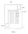
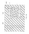
- FIG. 1is a plan view showing an example of a step in the method of manufacturing a semiconductor device according to the first embodiment.
- FIG. 2are cross-sectional views showing examples of cross sections taken along the A-A′ line and the B-B′ line in FIG. 1 .
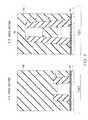
- FIG. 3is a plan view showing an example of a step following the step shown in FIG. 1 in the method of manufacturing a semiconductor device.
- FIG. 4are cross-sectional views showing examples of cross sections taken along the A-A′ line and the B-B′ line in FIG. 3 .
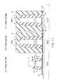
- FIG. 5is cross-sectional views showing examples of cross sections taken along the A-A′ line and the B-B′ line in steps following the step shown in FIG. 3 in the method of manufacturing a semiconductor device.
- FIG. 6is cross-sectional views showing examples of cross sections taken along the A-At line and the B-B′ line in steps following the step shown in FIG. 3 in the method of manufacturing a semiconductor device, is continuous from FIG. 5 .
- FIG. 7is cross-sectional views showing examples of cross sections taken along the A-A′ line and the B-B′ line in steps following the step shown in FIG. 3 in the method of manufacturing a semiconductor device, is continuous from FIG. 6 .
- FIG. 8is cross-sectional views showing examples of cross sections taken along the A-A′ line and the B-B′ line in steps following the step shown in FIG. 3 in the method of manufacturing a semiconductor device, is continuous from FIG. 7 .
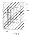
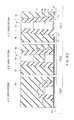
- FIG. 9is a plan view showing another example of a step in the method of manufacturing a semiconductor device according to the first embodiment.
- FIG. 10is a plan view showing an example of a step in a method of manufacturing a semiconductor device according to the second embodiment.
- FIG. 11is cross-sectional views showing examples of cross sections taken along the A-A′ line, the B-B′ line and the C-C′ line in FIG. 10 in steps in the method of manufacturing a semiconductor device according to the second embodiment.
- FIG. 12is cross-sectional views showing examples of cross sections taken along the A-A′ line, the B-B′ line and the C-C′ line in FIG. 10 in steps in the method of manufacturing a semiconductor device according to the second embodiment, is continuous from FIG. 11 .
- FIG. 13is cross-sectional views showing examples of cross sections taken along the A-A′ line, the B-B′ line and the C-C line in FIG. 10 in steps in the method of manufacturing a semiconductor device according to the second embodiment, is continuous from FIG. 12 .
- FIG. 14is cross-sectional views showing examples of cross sections taken along the A-A′ line, the B-B′ line and the C-C′ line in FIG. 10 in steps in the method of manufacturing a semiconductor device according to the second embodiment, is continuous from FIG. 13 .
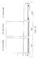
- FIG. 15is a plan view showing an example of a step following the step shown in FIG. 14 in the method of manufacturing a semiconductor device according to the second embodiment.
- FIG. 16is cross-sectional views showing examples of cross sections taken along the A-A′ line, the B-B′ line and the C-C′ line in FIG. 15 in steps in the method of manufacturing a semiconductor device according to the second embodiment.
- FIG. 17is cross-sectional views showing examples of cross sections taken along the A-A′ line, the B-B′ line and the C-C′ line in FIG. 15 in steps in the method of manufacturing a semiconductor device according to the second embodiment, is continuous from FIG. 16 .
- FIG. 18is cross-sectional views showing examples of cross sections taken along the A-A′ line, the B-B′ line and the C-C′ line in FIG. 15 in steps in the method of manufacturing a semiconductor device according to the second embodiment, is continuous from FIG. 17 .
- FIG. 19is cross-sectional views showing examples of cross sections taken along the A-A′ line, the B-B′ line and the C-C′ line in FIG. 15 in steps in the method of manufacturing a semiconductor device according to the second embodiment, is continuous from FIG. 18 .
- FIG. 20is cross-sectional views showing examples of cross sections taken along the A-A′ line, the B-B′ line and the C-C′ line in FIG. 15 in steps in the method of manufacturing a semiconductor device according to the second embodiment, is continuous from FIG. 19 .
- FIG. 21is a block diagram showing an example of a configuration of a semiconductor storage device according to the third embodiment.
- the region from which the hard mask and the metal are removedis lower than the other regions.
- the region from which the hard mask and the metal are removedcan suffer from dishing in planarization by chemical mechanical polishing (CMP).
- the hard mask and side wall removal patterns for the poly-metal gate formed in the poly-metal gate processare improved.
- a technique of forming a polysilicon resistive element in a poly-metal gate process by removing a metal on a polysilicon while leaving a hard mask so as to prevent occurrence of dishing in a subsequent CMP stepwill be described.
- a method of manufacturing a semiconductor device in which a resistive element is formed from a silicon film used in a multilayer gate film of a MOS transistorwill be described, focusing on a resistive element region in which the resistive element is formed.
- FIG. 1is a plan view showing an example of a step in the method of manufacturing a semiconductor device according to the first embodiment.
- FIG. 2are cross-sectional views showing examples of cross sections taken along the A-A′ line and the B-B′ line in FIG. 1 .
- FIG. 3is a plan view showing an example of a step following the step shown in FIG. 1 in the method of manufacturing a semiconductor device.
- FIG. 4are cross-sectional views showing examples of cross sections taken along the A-A′ line and the B-B′ line in FIG. 3 .
- FIGS. 5 to 8includes cross-sectional views showing examples of cross sections taken along the A-As line and the B-B′ line in steps following the step shown in FIG. 3 in the method of manufacturing a semiconductor device.
- illustration of an element isolation insulating film 2 xis omitted.
- a multilayer filmis formed on a semiconductor substrate 1 with the element isolation insulating film 2 x for element isolation selectively formed thereon in a resistive element region, the multilayer film including a silicon film 3 , a barrier metal film 4 that prevents diffusion of a metal (tungsten, for example) into the silicon film 3 , a metal film 5 containing the metal and a hard mask film 6 stacked one on another in this order.
- a transistor region(not shown) of the semiconductor substrate 1 , a transistor is formed in a region where the element isolation insulating film 2 x is not formed.
- the multilayer filmis selectively etched to an upper surface of the semiconductor substrate 1 to form a multilayer gate film 100 a.
- a gate side wall insulating film 7is then formed on the side surface of the multilayer gate film 100 a.
- the silicon film 3is a polysilicon film.
- the silicon film 3may be another conductive silicon film, such as an amorphous silicon film.
- the barrier metal film 4contains a titanium (Ti) film 4 a formed on the silicon film 3 and a titanium nitride (TiN) film 4 b formed on the titanium film 4 a.
- the barrier metal film 4can be made of any other material, such as WN, that prevents diffusion into the metal film 5 .
- the metal film 5is a tungsten (W) film, for example.
- the hard mask film 6is a silicon nitride film, for example.
- the gate side wall insulating film 7is formed by an insulating film, such as a silicon nitride film or a silicon oxide film.
- the multilayer gate film 100 a including the silicon film 3is formed in a substantially zigzag configuration on the semiconductor substrate 1 , for example.
- the silicon film 3is electrically connected to two resisting electrodes (contacts) 200 a and 200 b at the opposite ends thereof.
- the resisting electrodes 200 a and 200 bare electrically connected to a circuit arrangement of another semiconductor element (not shown).
- a resist film 8is selectively formed on the multilayer gate film 100 a and the gate side wall insulating film 7 extending on the semiconductor substrate 1 .
- the multilayer gate film 100 a and the gate side wall insulating film 7are exposed.
- the resist film 8is selectively formed on the multilayer gate film 100 a and the gate side wall insulating film 7 .
- the resist film 8is formed in a line/space pattern on the semiconductor substrate 1 ( FIG. 3 ).
- This patternallows etching in a subsequent wet etching step to proceed from the openings (space parts) in the resist film 8 and the etchant to penetrate to the region under the resist film 8 .
- an upper part of the gate side wall insulating film 7 and the hard mask film 6are selectively removed by dry etching, for example, so as to expose the surface of the metal film 5 .
- the gate side wall insulating film 7is etched in such a manner that at least the surface, including the top surface and side surfaces, of the silicon film 3 is not exposed.
- processing of the silicon film 3occurs only during formation of the multilayer gate film 100 a.
- Metal removal in a subsequent stepis performed by highly selective wet etching, so that size variations due to processing of the silicon film 3 can be reduced. That is, variations of the characteristics of the resistive element due to processing of the silicon film 3 can be reduced.
- the metal film 5 and the barrier metal film 4 adjoining the metal film 5are removed by wet etching in the region where the metal film 5 is exposed and in a region “x” above the silicon film 3 where the hard mask film 6 remains.
- the etchant used for the wet etchingis sulfuric acid/hydrogen peroxide, for example.
- the metal film 5 and the barrier metal film 4are removed from an upper surface 3 a of the silicon film 3 .
- a polysilicon resistor having a high resistancecan be formed in the semiconductor element formed in the poly-metal gate process. That is, a resistive element having a high resistance can be formed while reducing the increase of the circuit footprint.
- the metal film 5 and the barrier metal film 4are selectively removed by highly selective wet etching as described above, size variations due to processing of the silicon film 3 can be reduced. That is variations of the characteristics of the resistive element due to processing of the silicon film 3 can be reduced.
- the resist film 8is removed. After the resist film 8 is removed, as shown in FIG. 7 , spin coating or the like is performed to fill the space formed by removal of the metal film 5 and the barrier metal film 4 with a pre-metal dielectric (PMD) 9 a and deposit a PMD 9 b to a level higher than an upper surface 6 a of the remaining hard mask film 6 .
- PMDpre-metal dielectric
- the PMDs 9 a and 9 bare silicon oxide films, for example.
- a top part of the PMD 9 bis planarized by CMP using the remaining hard mask film 6 as a stopper.
- the hard mask film 6remains on the metal film 5 , so that the dishing that occurs in the comparative example described above can be prevented from occurring.
- the resistive element formed in the method of manufacturing a semiconductor device according to this embodiment described aboveincludes the semiconductor substrate 1 , the multilayer structure film extending on the semiconductor substrate 1 , the multilayer structure film being formed by the silicon film 3 stacked on the semiconductor substrate 1 , the PMD 9 a stacked on the silicon film 3 and the hard mask film 6 stacked on the PMD 9 a, the gate side wall insulating film 7 formed on the side surface of the multilayer structure film, and the PMD 9 b deposited on the semiconductor substrate 1 to the level of the upper surface of the hard mask.
- the resistive elementIn the resistive element, a part of the gate side wall insulating film 7 and a part of the hard mask film 6 are selectively removed so that the PMDs 9 a and 9 b are connected to each other, the PMDs 9 a and 9 b are made of the same material, and the silicon film 3 is electrically connected to the two resisting electrodes 200 a and 200 b at the opposite ends thereof.
- the resistive element formed in the method of manufacturing a semiconductor device according to the first embodimentis suitable for a multilayer structure, because dishing is unlikely to occur in the CMP planarization.
- FIG. 9is a plan view showing another example of a step in the method of manufacturing a semiconductor device according to the first embodiment.
- the same reference numeralsdenote the same components as those in FIG. 1 .
- the resist film 8can also be formed in a slit pattern on the semiconductor substrate 1 , for example.
- This patternalso allows etching in the subsequent wet etching step to proceed from the openings (space parts) in the resist film 8 and the etchant to penetrate to the region under the resist film 8 .
- a resistive element having desired characteristicscan be formed with a polysilicon resistor while reducing the increase of the circuit footprint.
- the above first embodimenthas been described focusing on the resistive element region in which the resistive element is formed.
- the barrier metal filmis formed directly on the silicon film. Therefore, a silicide film is formed at the interface between the silicon film and the barrier metal film. The silicide film is hardly removed by wet etching and can remain. Thus, the resistance of the resistive element is difficult to control.
- an example of a method that prevents formation of such a silicide film in the resistive element regionwill be described.
- the second embodimentwill be described focusing on two regions, the resistive element region and the transistor region in which a MOS transistor is formed.
- FIG. 10is a plan view showing an example of a step in a method of manufacturing a semiconductor device according to the second embodiment.
- FIGS. 11 to 14are cross-sectional views showing examples of cross sections taken along the A-A′ line, the B-B′ line and the C-C′ line in FIG. 10 in steps in the method of manufacturing a semiconductor device according to the second embodiment.
- FIG. 15is a plan view showing an example of a step following the step shown in FIG. 14 in the method of manufacturing a semiconductor device according to the second embodiment.
- FIGS. 16 to 20are cross-sectional views showing examples of cross sections taken along the A-A′ line, the B-B′ line and the C-C′ line in FIG. 15 in steps in the method of manufacturing a semiconductor device according to the second embodiment.
- the same reference numerals as those in FIGS. 1 to 8denote the same components as those in the first embodiment.
- FIG. 10shows a state where multilayer gate films 100 a and 100 b and gate side wall insulating films 7 are formed in a resistive element region 1000 and a transistor region 2000 in which a MOS transistor is to be formed on a semiconductor substrate 1 with an element isolation insulating film 2 x selectively formed thereon.
- the method of manufacturing a semiconductor device according to the second embodimentwill be described focusing on the resistive element region 1000 and the transistor region 2000 .
- a silicon film 3 and a protective film 10are formed in the resistive element region 1000 on the semiconductor substrate 1 with the element isolation insulating film 2 x formed thereon, and a gate insulating film 2 , a silicon film 3 and a protective film 10 are formed in the transistor region 2000 in which a MOS transistor is to be formed on the semiconductor substrate 1 with the element isolation insulating film 2 x selectively formed thereon.
- the protective film 10is an insulating film, such as a silicon oxide film and a silicon nitride film.
- the conditions of ion implantation to the silicon film 3 in the resistive element region 1000can be different from the conditions of ion implantation to the silicon film 3 in the transistor region 2000 . That is, the impurity concentration of the silicon film 3 in the transistor region 2000 can be different from the impurity concentration of the silicon film 3 in the resistive element region 1000 .
- the resistance of the resistive element formed in the resistive element region 1000can be designed and controlled independently of the conditions of manufacture of the transistor.
- a resist film 11is formed on the protective film 10 , and the protective film 10 on the silicon film 3 in the transistor region 2000 using the resist film 11 as a mask.
- the protective filmis removed in a part to be used for a poly-metal gate.
- the protective film 10exists, and therefore no silicide is formed at the interface between the barrier metal and the silicon.
- a barrier metal film 4 , a metal film 5 containing a metal and a hard mask film 6are stacked one on another in this order.
- the protective film 10 that prevents formation of silicideis formed on the silicon film 3 , and the barrier metal film 4 is formed on the protective film 10 .
- the resulting multilayer filmis selectively etched to the upper surface of the semiconductor substrate 1 , thereby forming multilayer gate films 100 a 1 and 100 b.
- the gate side wall insulating films 7are then formed on the side surfaces of the multilayer gate films 100 a 1 and 100 b, and a source-drain region la is formed in the transistor region 2000 by ion implantation.
- the multilayer gate film 100 b with the protective film 10 formed between the silicon film 3 and the barrier metal film 4is formed ( FIGS. 14( a ) and 14 ( b )), whereas in the transistor region 2000 , the multilayer gate film 100 a 1 with no protective film 10 formed between the silicon film 3 and the barrier metal film 4 is formed ( FIG. 14( c )).
- a resist film 8is selectively formed on the multilayer gate film 1001 : and the gate side wall insulating film 7 extending on the semiconductor substrate 1 ( FIGS. 16( a ) and 16 ( b )). And in the transistor region 2000 , a resist film 8 is formed to cover the whole of the top of the multilayer gate film 100 a 1 and the top of the gate side wall insulating film 7 ( FIG. 16( c )).
- the resist film 8is formed in a line/space pattern on the semiconductor substrate 1 ( FIG. 15 ).
- this patternallows etching in a subsequent wet etching step to proceed from the openings (space parts) in the resist film 8 and the etchant to penetrate to the region under the resist film 8 .
- an upper part of the gate side wall insulating film 7 and the hard mask film 6are selectively removed by dry etching, for example, so as to expose the surface of the metal film 5 .
- the gate side wall insulating film 7is etched in such a manner that at least the surface, including the top surface and side surfaces, of the silicon film 3 is not exposed.
- processing of the silicon film 3occurs only during formation of the multilayer gate film 100 b.
- Metal removal in a subsequent stepis performed by highly selective wet etching, so that size variations due to processing of the silicon film 3 can be reduced. That is, variations of the characteristics of the resistive element due to processing of the silicon film 3 can be reduced.
- the metal film 5 and the barrier metal film 4 adjoining the metal film 5are removed by wet etching in the region where the metal film 5 is exposed and in a region “x” above the silicon film 3 where the hard mask film 6 remains.
- the etchant used for the wet etchingis sulfuric acid/hydrogen peroxide, for example.
- the protective film 10such as a silicon oxide film is not removed.
- the metal film 5 and the barrier metal film 4are covered with the hard mask film 6 and the gate side wall insulating film 7 and therefore are not removed by the wet etching.
- the metal film 5 and the barrier metal film 4are removed from an upper surface 3 a of the silicon film 3 .
- a polysilicon resistor having a high resistancecan be formed in the semiconductor element formed in the poly-metal gate process. That is, a resistive element having a high resistance can be formed while reducing the increase of the circuit footprint.
- the metal film 5 and the barrier metal film 4are selectively removed by highly selective wet etching as described above, size variations due to processing of the silicon film 3 can be reduced. That is, variations of the characteristics of the resistive element due to processing of the silicon film 3 can be reduced.
- the protective film 10 between the barrier metal film 4 and the silicon film 3prevents formation of a silicide film that affects the resistance of the resistive element. That is, the resistance can be easily controlled.
- the resist film 8is removed. After the resist film 8 is removed, as shown in FIG. 19 , spin coating or the like is performed to fill the space formed by removal of the metal film 5 and the barrier metal film 4 with a PMD 9 a and deposit a PMD 9 b to a level higher than an upper surface 6 a of the remaining hard mask film 6 .
- a top part of the PMD 9 bis planarized by CMP using the remaining hard mask film 6 as a stopper.
- the hard mask film 6remains on the metal film 5 , so that the dishing that occurs in the comparative example described above can be prevented from occurring.
- the resistive element formed in the method of manufacturing a semiconductor deviceincludes the semiconductor substrate 1 with the element isolation insulating film 2 x formed thereon, the multilayer structure film extending on the semiconductor substrate 1 , the multilayer structure film being formed by the silicon film 3 stacked on the semiconductor substrate 1 , the protective film 10 stacked on the silicon film 3 the PMD 9 a stacked on the protective film 10 , the PMD 9 a stacked on the protective film 9 a and the hard mask film 6 stacked on the PMD 9 a, the gate side wall insulating film 7 formed on the side surface of the multilayer structure film, and the PMD 9 b deposited on the semiconductor substrate 1 to the level of the upper surface of the hard mask.
- the resistive elementa part of the gate side wall insulating film 7 and a part of the hard mask film 6 are selectively removed so that the PMDs 9 a and 9 b are connected to each other, the PMDs 9 a and 9 b are made of the same material, and the silicon film 3 is electrically connected to two resisting electrodes 200 a and 200 b at the opposite ends thereof.
- the resistive element formed in the method of manufacturing a semiconductor device according to the second embodimentis suitable for a multilayer structure, because dishing is unlikely to occur in the CMP planarization.
- a resistive element having desired characteristicscan be formed with a polysilicon resistor while reducing the increase of the circuit footprint.
- FIG. 21is a block diagram showing an example of a configuration of a semiconductor storage device according to the third embodiment.
- a semiconductor storage device (MRAM, for example) “M”includes a resistive element “R” formed on a semiconductor substrate 1 according to the first or second embodiment described above and a MOS transistor “Tr” formed on the semiconductor substrate 1 .
- the resistive element “R”is formed at the same time with the MOS transistor “Tr”, and the circuit footprint of the resistive element “R” can be reduced. Furthermore, since occurrence of dishing can be prevented in the CMP planarization, the semiconductor storage device “M” is suitable for forming a multilayer structure.
Landscapes
- Engineering & Computer Science (AREA)
- Manufacturing & Machinery (AREA)
- Metal-Oxide And Bipolar Metal-Oxide Semiconductor Integrated Circuits (AREA)
- Semiconductor Integrated Circuits (AREA)
- Mram Or Spin Memory Techniques (AREA)
Abstract
Description
Claims (16)
Applications Claiming Priority (3)
| Application Number | Priority Date | Filing Date | Title |
|---|---|---|---|
| JP2011121905AJP2012248814A (en) | 2011-05-31 | 2011-05-31 | Semiconductor device and manufacturing method of the same |
| JP2011-121905 | 2011-05-31 | ||
| PCT/JP2012/055164WO2012164989A1 (en) | 2011-05-31 | 2012-03-01 | Semiconductor device and method for manufacturing same |
Publications (2)
| Publication Number | Publication Date |
|---|---|
| US20140077145A1 US20140077145A1 (en) | 2014-03-20 |
| US9048424B2true US9048424B2 (en) | 2015-06-02 |
Family
ID=47258855
Family Applications (1)
| Application Number | Title | Priority Date | Filing Date |
|---|---|---|---|
| US14/122,567Expired - Fee RelatedUS9048424B2 (en) | 2011-05-31 | 2012-03-01 | Semiconductor device and method of manufacturing the same |
Country Status (4)
| Country | Link |
|---|---|
| US (1) | US9048424B2 (en) |
| JP (1) | JP2012248814A (en) |
| TW (1) | TWI470700B (en) |
| WO (1) | WO2012164989A1 (en) |
Citations (47)
| Publication number | Priority date | Publication date | Assignee | Title |
|---|---|---|---|---|
| US4419812A (en)* | 1982-08-23 | 1983-12-13 | Ncr Corporation | Method of fabricating an integrated circuit voltage multiplier containing a parallel plate capacitor |
| US5075250A (en)* | 1991-01-02 | 1991-12-24 | Xerox Corporation | Method of fabricating a monolithic integrated circuit chip for a thermal ink jet printhead |
| US5514612A (en)* | 1993-03-03 | 1996-05-07 | California Micro Devices, Inc. | Method of making a semiconductor device with integrated RC network and schottky diode |
| US5780333A (en)* | 1996-06-29 | 1998-07-14 | Hyundai Electronics Industries Co., Ltd. | Method of fabricating an analog semiconductor device having a salicide layer |
| US6001663A (en)* | 1995-06-07 | 1999-12-14 | Advanced Micro Devices, Inc. | Apparatus for detecting defect sizes in polysilicon and source-drain semiconductor devices and method for making the same |
| US6110772A (en)* | 1997-01-31 | 2000-08-29 | Sanyo Electric Co., Ltd. | Semiconductor integrated circuit and manufacturing method thereof |
| US6124160A (en)* | 1995-09-19 | 2000-09-26 | Matsushita Electric Industrial Co., Ltd. | Semiconductor device and method for manufacturing the same |
| US6279585B1 (en)* | 1998-09-09 | 2001-08-28 | Denso Corporation | Etching method and method for manufacturing semiconductor device using the same |
| US20010046771A1 (en)* | 1999-09-23 | 2001-11-29 | Philipp Steinmann | Thin film resistor having improved temperature independence and a method of engineering the TCR of the thin film resistor |
| US20020151148A1 (en)* | 2001-04-11 | 2002-10-17 | Conexant Systems, Inc. | Low cost fabrication of high resistivity resistors |
| US6497824B1 (en)* | 1999-09-23 | 2002-12-24 | Texas Instruments Incorporated | One mask solution for the integration of the thin film resistor |
| US20030052386A1 (en)* | 2001-09-20 | 2003-03-20 | Mitsubishi Denki Kabushiki Kaisha | Semiconductor device with resistor layer having heat radiation path to semiconductor substrate |
| US20030222317A1 (en)* | 2002-06-03 | 2003-12-04 | Mitsubishi Denki Kabushiki Kaisha | Semiconductor memory device with improved soft-error resistance |
| JP2004140508A (en) | 2002-10-16 | 2004-05-13 | Tdk Corp | Demultiplexer |
| US20040140508A1 (en) | 2003-01-14 | 2004-07-22 | Matsushita Electric Industrial Co., Ltd. | Semiconductor device and method for fabricating the same |
| US20050101034A1 (en)* | 2003-11-10 | 2005-05-12 | Sanjeev Aggarwal | Hardmask for forming ferroelectric capacitors in a semiconductor device and methods for fabricating the same |
| JP2005142346A (en) | 2003-11-06 | 2005-06-02 | Fujitsu Ltd | Unipolar transistor and semiconductor integrated circuit device |
| US20050263823A1 (en)* | 2004-05-27 | 2005-12-01 | Young-Nam Hwang | Phase-change memory device having a barrier layer and manufacturing method |
| US20060145296A1 (en)* | 2005-01-06 | 2006-07-06 | International Business Machines Corporation | Tunable temperature coefficient of resistance resistors and method of fabricating same |
| US20070128790A1 (en)* | 2004-09-30 | 2007-06-07 | Masanori Dainin | Semiconductor device and fabrication process thereof |
| JP2007324292A (en) | 2006-05-31 | 2007-12-13 | Seiko Epson Corp | Manufacturing method of semiconductor device |
| US20080003762A1 (en)* | 2005-12-28 | 2008-01-03 | Hynix Semiconductor Inc. | Method of forming resistor of flash memory device |
| US20090001517A1 (en)* | 2007-06-27 | 2009-01-01 | Leland Scott Swanson | Thermally enhanced semiconductor devices |
| US20090090977A1 (en)* | 2007-10-09 | 2009-04-09 | International Business Machines Corporation | Resistor and fet formed from the metal portion of a mosfet metal gate stack |
| US20090101994A1 (en)* | 2007-10-19 | 2009-04-23 | Kyoung-Mi Moon | Semiconductor device and method for fabricating the same |
| US20090230542A1 (en)* | 2008-03-13 | 2009-09-17 | Stats Chippac, Ltd. | Semiconductor Device With Integrated Passive Circuit and Method of Making the Same Using Sacrificial Substrate |
| US20090286378A1 (en)* | 2008-05-19 | 2009-11-19 | Nec Electronics Corporation | Semiconductor device and method of manufacturing the same |
| US20090283840A1 (en)* | 2008-05-13 | 2009-11-19 | International Business Machines Corporation | Metal gate integration structure and method including metal fuse, anti-fuse and/or resistor |
| US20090302384A1 (en)* | 2008-06-05 | 2009-12-10 | Rohm Co., Ltd. | Semiconductor device and method for producing semiconductor device |
| US20100009510A1 (en)* | 2008-07-09 | 2010-01-14 | Nec Electronics Corporation | Method of manufacturing semiconductor device |
| JP2010272598A (en) | 2009-05-19 | 2010-12-02 | Renesas Electronics Corp | Semiconductor device and manufacturing method thereof |
| US20100308436A1 (en)* | 2009-06-08 | 2010-12-09 | Panasonic Corporation | Semiconductor device and manufacturing method thereof |
| US20100320509A1 (en)* | 2009-06-17 | 2010-12-23 | Globalfoundries Inc. (Grand Cayman, Cayman Islands ) | Method for forming and integrating metal gate transistors having self-aligned contacts and related structure |
| US20100320544A1 (en)* | 2009-06-22 | 2010-12-23 | Chih-Yu Tseng | Metal gate transistor and resistor and method for fabricating the same |
| US20100328022A1 (en)* | 2009-06-24 | 2010-12-30 | Cheng-Wen Fan | Method for fabricating metal gate and polysilicon resistor and related polysilicon resistor structure |
| US20110057267A1 (en)* | 2009-09-04 | 2011-03-10 | Taiwan Semiconductor Manufacturing Company, Ltd. | Polysilicon design for replacement gate technology |
| US20110111567A1 (en)* | 2005-05-23 | 2011-05-12 | Fujitsu Limited | Semiconductor device and method of manufacturing the same |
| JP2011100910A (en) | 2009-11-09 | 2011-05-19 | Panasonic Corp | Semiconductor device, and method for manufacturing the same |
| US20110117710A1 (en)* | 2009-11-19 | 2011-05-19 | Yung-Chang Lin | Method of fabricating efuse, resistor and transistor |
| US20110189827A1 (en)* | 2010-02-04 | 2011-08-04 | Che-Hua Hsu | Method of fabricating efuse structure, resistor sturcture and transistor sturcture |
| US20110280064A1 (en)* | 2009-03-12 | 2011-11-17 | Fujitsu Limited | Composite resistance variable element and method for manufacturing the same |
| US20120009757A1 (en)* | 2008-04-04 | 2012-01-12 | Hynix Semiconductor Inc. | Phase-change memory device and method of fabricating the same |
| US20120126369A1 (en)* | 2006-12-21 | 2012-05-24 | Stats Chippac, Ltd. | Semiconductor Device and Method of Forming Passive Devices |
| US20120178234A1 (en)* | 2011-01-11 | 2012-07-12 | Samsung Electronics Co., Ltd. | Method of manufacturing an integrated circuit device |
| US20120292740A1 (en)* | 2011-05-19 | 2012-11-22 | Macronix International Co., Ltd. | High voltage resistance semiconductor device and method of manufacturing a high voltage resistance semiconductor device |
| US20120305880A1 (en)* | 2011-06-03 | 2012-12-06 | Wei Zhang | Resistive random access memory with electric-field strengthened layer and manufacturing method thereof |
| US8927385B2 (en)* | 2012-12-17 | 2015-01-06 | Texas Instruments Incorporated | ZTCR poly resistor in replacement gate flow |
Family Cites Families (3)
| Publication number | Priority date | Publication date | Assignee | Title |
|---|---|---|---|---|
| JP3420104B2 (en)* | 1999-04-21 | 2003-06-23 | 山形日本電気株式会社 | Manufacturing method of resistance element |
| US6548389B2 (en)* | 2000-04-03 | 2003-04-15 | Matsushita Electric Industrial Co., Ltd. | Semiconductor device and method for fabricating the same |
| TWI446447B (en)* | 2008-10-16 | 2014-07-21 | United Microelectronics Corp | Method for forming a thin film resistor |
- 2011
- 2011-05-31JPJP2011121905Apatent/JP2012248814A/ennot_activeWithdrawn
- 2012
- 2012-03-01USUS14/122,567patent/US9048424B2/ennot_activeExpired - Fee Related
- 2012-03-01WOPCT/JP2012/055164patent/WO2012164989A1/ennot_activeCeased
- 2012-03-15TWTW101108929Apatent/TWI470700B/ennot_activeIP Right Cessation
Patent Citations (52)
| Publication number | Priority date | Publication date | Assignee | Title |
|---|---|---|---|---|
| US4419812A (en)* | 1982-08-23 | 1983-12-13 | Ncr Corporation | Method of fabricating an integrated circuit voltage multiplier containing a parallel plate capacitor |
| US5075250A (en)* | 1991-01-02 | 1991-12-24 | Xerox Corporation | Method of fabricating a monolithic integrated circuit chip for a thermal ink jet printhead |
| US5514612A (en)* | 1993-03-03 | 1996-05-07 | California Micro Devices, Inc. | Method of making a semiconductor device with integrated RC network and schottky diode |
| US6001663A (en)* | 1995-06-07 | 1999-12-14 | Advanced Micro Devices, Inc. | Apparatus for detecting defect sizes in polysilicon and source-drain semiconductor devices and method for making the same |
| US6124160A (en)* | 1995-09-19 | 2000-09-26 | Matsushita Electric Industrial Co., Ltd. | Semiconductor device and method for manufacturing the same |
| US5780333A (en)* | 1996-06-29 | 1998-07-14 | Hyundai Electronics Industries Co., Ltd. | Method of fabricating an analog semiconductor device having a salicide layer |
| US6110772A (en)* | 1997-01-31 | 2000-08-29 | Sanyo Electric Co., Ltd. | Semiconductor integrated circuit and manufacturing method thereof |
| US6279585B1 (en)* | 1998-09-09 | 2001-08-28 | Denso Corporation | Etching method and method for manufacturing semiconductor device using the same |
| US20010046771A1 (en)* | 1999-09-23 | 2001-11-29 | Philipp Steinmann | Thin film resistor having improved temperature independence and a method of engineering the TCR of the thin film resistor |
| US6497824B1 (en)* | 1999-09-23 | 2002-12-24 | Texas Instruments Incorporated | One mask solution for the integration of the thin film resistor |
| US20020151148A1 (en)* | 2001-04-11 | 2002-10-17 | Conexant Systems, Inc. | Low cost fabrication of high resistivity resistors |
| US20030052386A1 (en)* | 2001-09-20 | 2003-03-20 | Mitsubishi Denki Kabushiki Kaisha | Semiconductor device with resistor layer having heat radiation path to semiconductor substrate |
| US20030222317A1 (en)* | 2002-06-03 | 2003-12-04 | Mitsubishi Denki Kabushiki Kaisha | Semiconductor memory device with improved soft-error resistance |
| JP2004140508A (en) | 2002-10-16 | 2004-05-13 | Tdk Corp | Demultiplexer |
| US20040140508A1 (en) | 2003-01-14 | 2004-07-22 | Matsushita Electric Industrial Co., Ltd. | Semiconductor device and method for fabricating the same |
| US7851891B2 (en) | 2003-01-14 | 2010-12-14 | Panasonic Corporation | Semiconductor device and method for fabricating the same |
| JP2004221234A (en) | 2003-01-14 | 2004-08-05 | Matsushita Electric Ind Co Ltd | Semiconductor device and manufacturing method thereof |
| US20090206454A1 (en) | 2003-01-14 | 2009-08-20 | Matsushita Electric Industrial Co., Ltd. | Semiconductor device and method for fabricating the same |
| JP2005142346A (en) | 2003-11-06 | 2005-06-02 | Fujitsu Ltd | Unipolar transistor and semiconductor integrated circuit device |
| US20050101034A1 (en)* | 2003-11-10 | 2005-05-12 | Sanjeev Aggarwal | Hardmask for forming ferroelectric capacitors in a semiconductor device and methods for fabricating the same |
| US20050263823A1 (en)* | 2004-05-27 | 2005-12-01 | Young-Nam Hwang | Phase-change memory device having a barrier layer and manufacturing method |
| US20070128790A1 (en)* | 2004-09-30 | 2007-06-07 | Masanori Dainin | Semiconductor device and fabrication process thereof |
| US20060145296A1 (en)* | 2005-01-06 | 2006-07-06 | International Business Machines Corporation | Tunable temperature coefficient of resistance resistors and method of fabricating same |
| US20110111567A1 (en)* | 2005-05-23 | 2011-05-12 | Fujitsu Limited | Semiconductor device and method of manufacturing the same |
| US20080003762A1 (en)* | 2005-12-28 | 2008-01-03 | Hynix Semiconductor Inc. | Method of forming resistor of flash memory device |
| JP2007324292A (en) | 2006-05-31 | 2007-12-13 | Seiko Epson Corp | Manufacturing method of semiconductor device |
| US20120126369A1 (en)* | 2006-12-21 | 2012-05-24 | Stats Chippac, Ltd. | Semiconductor Device and Method of Forming Passive Devices |
| US20090001517A1 (en)* | 2007-06-27 | 2009-01-01 | Leland Scott Swanson | Thermally enhanced semiconductor devices |
| US20090090977A1 (en)* | 2007-10-09 | 2009-04-09 | International Business Machines Corporation | Resistor and fet formed from the metal portion of a mosfet metal gate stack |
| US20090101994A1 (en)* | 2007-10-19 | 2009-04-23 | Kyoung-Mi Moon | Semiconductor device and method for fabricating the same |
| US20090230542A1 (en)* | 2008-03-13 | 2009-09-17 | Stats Chippac, Ltd. | Semiconductor Device With Integrated Passive Circuit and Method of Making the Same Using Sacrificial Substrate |
| US20120009757A1 (en)* | 2008-04-04 | 2012-01-12 | Hynix Semiconductor Inc. | Phase-change memory device and method of fabricating the same |
| US20090283840A1 (en)* | 2008-05-13 | 2009-11-19 | International Business Machines Corporation | Metal gate integration structure and method including metal fuse, anti-fuse and/or resistor |
| US7883983B2 (en) | 2008-05-19 | 2011-02-08 | Renesas Electronics Corporation | Semiconductor device and method of manufacturing the same |
| JP2009283497A (en) | 2008-05-19 | 2009-12-03 | Nec Electronics Corp | Semiconductor device and method of manufacturing the same |
| US20090286378A1 (en)* | 2008-05-19 | 2009-11-19 | Nec Electronics Corporation | Semiconductor device and method of manufacturing the same |
| US20090302384A1 (en)* | 2008-06-05 | 2009-12-10 | Rohm Co., Ltd. | Semiconductor device and method for producing semiconductor device |
| US20100009510A1 (en)* | 2008-07-09 | 2010-01-14 | Nec Electronics Corporation | Method of manufacturing semiconductor device |
| US20110280064A1 (en)* | 2009-03-12 | 2011-11-17 | Fujitsu Limited | Composite resistance variable element and method for manufacturing the same |
| JP2010272598A (en) | 2009-05-19 | 2010-12-02 | Renesas Electronics Corp | Semiconductor device and manufacturing method thereof |
| US20100308436A1 (en)* | 2009-06-08 | 2010-12-09 | Panasonic Corporation | Semiconductor device and manufacturing method thereof |
| US20100320509A1 (en)* | 2009-06-17 | 2010-12-23 | Globalfoundries Inc. (Grand Cayman, Cayman Islands ) | Method for forming and integrating metal gate transistors having self-aligned contacts and related structure |
| US20100320544A1 (en)* | 2009-06-22 | 2010-12-23 | Chih-Yu Tseng | Metal gate transistor and resistor and method for fabricating the same |
| US20100328022A1 (en)* | 2009-06-24 | 2010-12-30 | Cheng-Wen Fan | Method for fabricating metal gate and polysilicon resistor and related polysilicon resistor structure |
| US20110057267A1 (en)* | 2009-09-04 | 2011-03-10 | Taiwan Semiconductor Manufacturing Company, Ltd. | Polysilicon design for replacement gate technology |
| JP2011100910A (en) | 2009-11-09 | 2011-05-19 | Panasonic Corp | Semiconductor device, and method for manufacturing the same |
| US20110117710A1 (en)* | 2009-11-19 | 2011-05-19 | Yung-Chang Lin | Method of fabricating efuse, resistor and transistor |
| US20110189827A1 (en)* | 2010-02-04 | 2011-08-04 | Che-Hua Hsu | Method of fabricating efuse structure, resistor sturcture and transistor sturcture |
| US20120178234A1 (en)* | 2011-01-11 | 2012-07-12 | Samsung Electronics Co., Ltd. | Method of manufacturing an integrated circuit device |
| US20120292740A1 (en)* | 2011-05-19 | 2012-11-22 | Macronix International Co., Ltd. | High voltage resistance semiconductor device and method of manufacturing a high voltage resistance semiconductor device |
| US20120305880A1 (en)* | 2011-06-03 | 2012-12-06 | Wei Zhang | Resistive random access memory with electric-field strengthened layer and manufacturing method thereof |
| US8927385B2 (en)* | 2012-12-17 | 2015-01-06 | Texas Instruments Incorporated | ZTCR poly resistor in replacement gate flow |
Non-Patent Citations (2)
| Title |
|---|
| International Search Report and Written Opinion for corresponding PCT Application No. PCT/JP2012/055164, filed Mar. 1, 2012, dated Dec. 27, 2013, 5 pgs. |
| International Search Report for corresponding PCT Application No. PCT/JP2012/055164, dated Jun. 5, 2012, 2pgs. |
Also Published As
| Publication number | Publication date |
|---|---|
| WO2012164989A1 (en) | 2012-12-06 |
| TW201248738A (en) | 2012-12-01 |
| JP2012248814A (en) | 2012-12-13 |
| US20140077145A1 (en) | 2014-03-20 |
| TWI470700B (en) | 2015-01-21 |
Similar Documents
| Publication | Publication Date | Title |
|---|---|---|
| US10475794B1 (en) | Semiconductor device and method for fabricating the same | |
| US7291556B2 (en) | Method for forming small features in microelectronic devices using sacrificial layers | |
| US7265050B2 (en) | Methods for fabricating memory devices using sacrificial layers | |
| US9859284B2 (en) | Semiconductor memory device having enlarged cell contact area and method of fabricating the same | |
| US8859386B2 (en) | Semiconductor devices, methods of manufacture thereof, and methods of forming resistors | |
| US6995422B2 (en) | High-density three-dimensional memory | |
| US10263001B2 (en) | Method of forming semiconductor memory device | |
| US8174064B2 (en) | Semiconductor device and method for forming the same | |
| US10770464B2 (en) | Semiconductor device including bit line structure of dynamic random access memory (DRAM) and method for fabricating the same | |
| US10790301B2 (en) | Methods for forming three-dimensional memory device without conductor residual caused by dishing | |
| US8629488B2 (en) | Method for manufacturing an energy storage device and structure therefor | |
| US10832946B1 (en) | Recessed interconnet line having a low-oxygen cap for facilitating a robust planarization process and protecting the interconnect line from downstream etch operations | |
| US10008409B2 (en) | Method for fabricating a semiconductor device | |
| US9653600B2 (en) | Semiconductor device and method of fabricating same | |
| US11127675B2 (en) | Interconnection structure and manufacturing method thereof | |
| US20150214234A1 (en) | Semiconductor device and method for fabricating the same | |
| US9048424B2 (en) | Semiconductor device and method of manufacturing the same | |
| US7935634B2 (en) | Integrated circuits, micromechanical devices, and method of making same | |
| US20070284743A1 (en) | Fabricating Memory Devices Using Sacrificial Layers and Memory Devices Fabricated by Same | |
| US20170025352A1 (en) | Antifuse structures and methods of making same | |
| KR100382542B1 (en) | method for manufacturing of semiconductor device | |
| KR100835779B1 (en) | Manufacturing Method of Semiconductor Device | |
| US20070010089A1 (en) | Method of forming bit line of semiconductor device | |
| KR20100079388A (en) | Resistor of nonvolatile memory device and the fabricating method thereof |
Legal Events
| Date | Code | Title | Description |
|---|---|---|---|
| AS | Assignment | Owner name:KABUSHIKI KAISHA TOSHIBA, JAPAN Free format text:ASSIGNMENT OF ASSIGNORS INTEREST;ASSIGNORS:OKADA, TAKAYUKI;MOROOKA, TETSU;SIGNING DATES FROM 20131115 TO 20131119;REEL/FRAME:031686/0229 | |
| STCF | Information on status: patent grant | Free format text:PATENTED CASE | |
| AS | Assignment | Owner name:TOSHIBA MEMORY CORPORATION, JAPAN Free format text:ASSIGNMENT OF ASSIGNORS INTEREST;ASSIGNOR:KABUSHIKI KAISHA TOSHIBA;REEL/FRAME:043709/0035 Effective date:20170706 | |
| MAFP | Maintenance fee payment | Free format text:PAYMENT OF MAINTENANCE FEE, 4TH YEAR, LARGE ENTITY (ORIGINAL EVENT CODE: M1551); ENTITY STATUS OF PATENT OWNER: LARGE ENTITY Year of fee payment:4 | |
| FEPP | Fee payment procedure | Free format text:MAINTENANCE FEE REMINDER MAILED (ORIGINAL EVENT CODE: REM.); ENTITY STATUS OF PATENT OWNER: LARGE ENTITY | |
| LAPS | Lapse for failure to pay maintenance fees | Free format text:PATENT EXPIRED FOR FAILURE TO PAY MAINTENANCE FEES (ORIGINAL EVENT CODE: EXP.); ENTITY STATUS OF PATENT OWNER: LARGE ENTITY | |
| STCH | Information on status: patent discontinuation | Free format text:PATENT EXPIRED DUE TO NONPAYMENT OF MAINTENANCE FEES UNDER 37 CFR 1.362 | |
| FP | Lapsed due to failure to pay maintenance fee | Effective date:20230602 |