US9044822B2 - Transient liquid phase bonding process for double sided power modules - Google Patents
Transient liquid phase bonding process for double sided power modulesDownload PDFInfo
- Publication number
- US9044822B2 US9044822B2US13/957,320US201313957320AUS9044822B2US 9044822 B2US9044822 B2US 9044822B2US 201313957320 AUS201313957320 AUS 201313957320AUS 9044822 B2US9044822 B2US 9044822B2
- Authority
- US
- United States
- Prior art keywords
- bonding
- melting point
- objective
- temperature
- electronic device
- Prior art date
- Legal status (The legal status is an assumption and is not a legal conclusion. Google has not performed a legal analysis and makes no representation as to the accuracy of the status listed.)
- Active, expires
Links
- 238000000034methodMethods0.000titleclaimsabstractdescription126
- 230000008569processEffects0.000titleclaimsabstractdescription90
- 239000007791liquid phaseSubstances0.000titleclaimsabstractdescription10
- 230000001052transient effectEffects0.000titleclaimsabstractdescription10
- 239000000463materialSubstances0.000claimsdescription171
- 238000002844meltingMethods0.000claimsdescription47
- 230000008018meltingEffects0.000claimsdescription43
- 238000007711solidificationMethods0.000claimsdescription31
- 230000008023solidificationEffects0.000claimsdescription31
- 239000002184metalSubstances0.000claimsdescription30
- 229910052751metalInorganic materials0.000claimsdescription30
- 238000001816coolingMethods0.000claimsdescription5
- PCHJSUWPFVWCPO-UHFFFAOYSA-NgoldChemical compound[Au]PCHJSUWPFVWCPO-UHFFFAOYSA-N0.000claimsdescription3
- 239000010931goldSubstances0.000claimsdescription3
- 229910052737goldInorganic materials0.000claimsdescription3
- 238000004519manufacturing processMethods0.000abstractdescription14
- 238000012545processingMethods0.000abstractdescription8
- 229910045601alloyInorganic materials0.000description30
- 239000000956alloySubstances0.000description30
- 239000010410layerSubstances0.000description26
- 229910000679solderInorganic materials0.000description14
- 238000009792diffusion processMethods0.000description9
- 238000005476solderingMethods0.000description8
- KUNSUQLRTQLHQQ-UHFFFAOYSA-Ncopper tinChemical compound[Cu].[Sn]KUNSUQLRTQLHQQ-UHFFFAOYSA-N0.000description5
- 238000010586diagramMethods0.000description5
- 125000006850spacer groupChemical group0.000description5
- 238000003860storageMethods0.000description5
- 239000000758substrateSubstances0.000description5
- 229910018082Cu3SnInorganic materials0.000description4
- 229910018471Cu6Sn5Inorganic materials0.000description4
- 230000008901benefitEffects0.000description4
- 238000013461designMethods0.000description4
- 229910000521B alloyInorganic materials0.000description3
- 238000005516engineering processMethods0.000description3
- 239000004065semiconductorSubstances0.000description3
- RYGMFSIKBFXOCR-UHFFFAOYSA-NCopperChemical compound[Cu]RYGMFSIKBFXOCR-UHFFFAOYSA-N0.000description2
- 229910017755Cu-SnInorganic materials0.000description2
- 229910017927Cu—SnInorganic materials0.000description2
- 229910052802copperInorganic materials0.000description2
- 239000010949copperSubstances0.000description2
- 230000005669field effectEffects0.000description2
- 238000007689inspectionMethods0.000description2
- 239000011229interlayerSubstances0.000description2
- 239000000155meltSubstances0.000description2
- 239000000203mixtureSubstances0.000description2
- 238000002203pretreatmentMethods0.000description2
- 229910052710siliconInorganic materials0.000description2
- 239000010703siliconSubstances0.000description2
- 230000009466transformationEffects0.000description2
- 230000007704transitionEffects0.000description2
- ATJFFYVFTNAWJD-UHFFFAOYSA-NTinChemical compound[Sn]ATJFFYVFTNAWJD-UHFFFAOYSA-N0.000description1
- QCEUXSAXTBNJGO-UHFFFAOYSA-N[Ag].[Sn]Chemical compound[Ag].[Sn]QCEUXSAXTBNJGO-UHFFFAOYSA-N0.000description1
- 229910052782aluminiumInorganic materials0.000description1
- XAGFODPZIPBFFR-UHFFFAOYSA-NaluminiumChemical compound[Al]XAGFODPZIPBFFR-UHFFFAOYSA-N0.000description1
- 230000015572biosynthetic processEffects0.000description1
- 238000005219brazingMethods0.000description1
- 230000008859changeEffects0.000description1
- 150000001875compoundsChemical class0.000description1
- 230000007423decreaseEffects0.000description1
- 230000001419dependent effectEffects0.000description1
- 230000000994depressogenic effectEffects0.000description1
- GPYPVKIFOKLUGD-UHFFFAOYSA-Ngold indiumChemical compound[In].[Au]GPYPVKIFOKLUGD-UHFFFAOYSA-N0.000description1
- JVPLOXQKFGYFMN-UHFFFAOYSA-Ngold tinChemical compound[Sn].[Au]JVPLOXQKFGYFMN-UHFFFAOYSA-N0.000description1
- YZASAXHKAQYPEH-UHFFFAOYSA-Nindium silverChemical compound[Ag].[In]YZASAXHKAQYPEH-UHFFFAOYSA-N0.000description1
- 239000007788liquidSubstances0.000description1
- 238000010309melting processMethods0.000description1
- 229910001092metal group alloyInorganic materials0.000description1
- 150000002739metalsChemical class0.000description1
- 238000012986modificationMethods0.000description1
- 230000004048modificationEffects0.000description1
- CLDVQCMGOSGNIW-UHFFFAOYSA-Nnickel tinChemical compound[Ni].[Sn]CLDVQCMGOSGNIW-UHFFFAOYSA-N0.000description1
- 239000012071phaseSubstances0.000description1
- 238000004886process controlMethods0.000description1
- 230000036632reaction speedEffects0.000description1
- 230000009467reductionEffects0.000description1
- 239000007787solidSubstances0.000description1
- 238000013519translationMethods0.000description1
Images


Classifications
- B—PERFORMING OPERATIONS; TRANSPORTING
- B23—MACHINE TOOLS; METAL-WORKING NOT OTHERWISE PROVIDED FOR
- B23K—SOLDERING OR UNSOLDERING; WELDING; CLADDING OR PLATING BY SOLDERING OR WELDING; CUTTING BY APPLYING HEAT LOCALLY, e.g. FLAME CUTTING; WORKING BY LASER BEAM
- B23K20/00—Non-electric welding by applying impact or other pressure, with or without the application of heat, e.g. cladding or plating
- B23K20/02—Non-electric welding by applying impact or other pressure, with or without the application of heat, e.g. cladding or plating by means of a press ; Diffusion bonding
- B23K20/023—Thermo-compression bonding
- B23K20/026—Thermo-compression bonding with diffusion of soldering material
- B—PERFORMING OPERATIONS; TRANSPORTING
- B23—MACHINE TOOLS; METAL-WORKING NOT OTHERWISE PROVIDED FOR
- B23K—SOLDERING OR UNSOLDERING; WELDING; CLADDING OR PLATING BY SOLDERING OR WELDING; CUTTING BY APPLYING HEAT LOCALLY, e.g. FLAME CUTTING; WORKING BY LASER BEAM
- B23K20/00—Non-electric welding by applying impact or other pressure, with or without the application of heat, e.g. cladding or plating
- B23K20/02—Non-electric welding by applying impact or other pressure, with or without the application of heat, e.g. cladding or plating by means of a press ; Diffusion bonding
- B—PERFORMING OPERATIONS; TRANSPORTING
- B23—MACHINE TOOLS; METAL-WORKING NOT OTHERWISE PROVIDED FOR
- B23K—SOLDERING OR UNSOLDERING; WELDING; CLADDING OR PLATING BY SOLDERING OR WELDING; CUTTING BY APPLYING HEAT LOCALLY, e.g. FLAME CUTTING; WORKING BY LASER BEAM
- B23K1/00—Soldering, e.g. brazing, or unsoldering
- B23K1/0008—Soldering, e.g. brazing, or unsoldering specially adapted for particular articles or work
- B23K1/0016—Brazing of electronic components
- B—PERFORMING OPERATIONS; TRANSPORTING
- B23—MACHINE TOOLS; METAL-WORKING NOT OTHERWISE PROVIDED FOR
- B23K—SOLDERING OR UNSOLDERING; WELDING; CLADDING OR PLATING BY SOLDERING OR WELDING; CUTTING BY APPLYING HEAT LOCALLY, e.g. FLAME CUTTING; WORKING BY LASER BEAM
- B23K20/00—Non-electric welding by applying impact or other pressure, with or without the application of heat, e.g. cladding or plating
- B23K20/16—Non-electric welding by applying impact or other pressure, with or without the application of heat, e.g. cladding or plating with interposition of special material to facilitate connection of the parts, e.g. material for absorbing or producing gas
- B—PERFORMING OPERATIONS; TRANSPORTING
- B23—MACHINE TOOLS; METAL-WORKING NOT OTHERWISE PROVIDED FOR
- B23K—SOLDERING OR UNSOLDERING; WELDING; CLADDING OR PLATING BY SOLDERING OR WELDING; CUTTING BY APPLYING HEAT LOCALLY, e.g. FLAME CUTTING; WORKING BY LASER BEAM
- B23K20/00—Non-electric welding by applying impact or other pressure, with or without the application of heat, e.g. cladding or plating
- B23K20/22—Non-electric welding by applying impact or other pressure, with or without the application of heat, e.g. cladding or plating taking account of the properties of the materials to be welded
- H—ELECTRICITY
- H01—ELECTRIC ELEMENTS
- H01L—SEMICONDUCTOR DEVICES NOT COVERED BY CLASS H10
- H01L24/00—Arrangements for connecting or disconnecting semiconductor or solid-state bodies; Methods or apparatus related thereto
- H01L24/01—Means for bonding being attached to, or being formed on, the surface to be connected, e.g. chip-to-package, die-attach, "first-level" interconnects; Manufacturing methods related thereto
- H01L24/26—Layer connectors, e.g. plate connectors, solder or adhesive layers; Manufacturing methods related thereto
- H01L24/31—Structure, shape, material or disposition of the layer connectors after the connecting process
- H01L24/33—Structure, shape, material or disposition of the layer connectors after the connecting process of a plurality of layer connectors
- H—ELECTRICITY
- H01—ELECTRIC ELEMENTS
- H01L—SEMICONDUCTOR DEVICES NOT COVERED BY CLASS H10
- H01L24/00—Arrangements for connecting or disconnecting semiconductor or solid-state bodies; Methods or apparatus related thereto
- H01L24/80—Methods for connecting semiconductor or other solid state bodies using means for bonding being attached to, or being formed on, the surface to be connected
- H01L24/83—Methods for connecting semiconductor or other solid state bodies using means for bonding being attached to, or being formed on, the surface to be connected using a layer connector
- H—ELECTRICITY
- H05—ELECTRIC TECHNIQUES NOT OTHERWISE PROVIDED FOR
- H05K—PRINTED CIRCUITS; CASINGS OR CONSTRUCTIONAL DETAILS OF ELECTRIC APPARATUS; MANUFACTURE OF ASSEMBLAGES OF ELECTRICAL COMPONENTS
- H05K13/00—Apparatus or processes specially adapted for manufacturing or adjusting assemblages of electric components
- H05K13/0023—
- B—PERFORMING OPERATIONS; TRANSPORTING
- B23—MACHINE TOOLS; METAL-WORKING NOT OTHERWISE PROVIDED FOR
- B23K—SOLDERING OR UNSOLDERING; WELDING; CLADDING OR PLATING BY SOLDERING OR WELDING; CUTTING BY APPLYING HEAT LOCALLY, e.g. FLAME CUTTING; WORKING BY LASER BEAM
- B23K2101/00—Articles made by soldering, welding or cutting
- B23K2101/36—Electric or electronic devices
- B23K2101/42—Printed circuits
- B23K2201/36—
- H—ELECTRICITY
- H01—ELECTRIC ELEMENTS
- H01L—SEMICONDUCTOR DEVICES NOT COVERED BY CLASS H10
- H01L2224/00—Indexing scheme for arrangements for connecting or disconnecting semiconductor or solid-state bodies and methods related thereto as covered by H01L24/00
- H01L2224/01—Means for bonding being attached to, or being formed on, the surface to be connected, e.g. chip-to-package, die-attach, "first-level" interconnects; Manufacturing methods related thereto
- H01L2224/02—Bonding areas; Manufacturing methods related thereto
- H01L2224/04—Structure, shape, material or disposition of the bonding areas prior to the connecting process
- H01L2224/04026—Bonding areas specifically adapted for layer connectors
- H—ELECTRICITY
- H01—ELECTRIC ELEMENTS
- H01L—SEMICONDUCTOR DEVICES NOT COVERED BY CLASS H10
- H01L2224/00—Indexing scheme for arrangements for connecting or disconnecting semiconductor or solid-state bodies and methods related thereto as covered by H01L24/00
- H01L2224/01—Means for bonding being attached to, or being formed on, the surface to be connected, e.g. chip-to-package, die-attach, "first-level" interconnects; Manufacturing methods related thereto
- H01L2224/26—Layer connectors, e.g. plate connectors, solder or adhesive layers; Manufacturing methods related thereto
- H01L2224/2612—Auxiliary members for layer connectors, e.g. spacers
- H—ELECTRICITY
- H01—ELECTRIC ELEMENTS
- H01L—SEMICONDUCTOR DEVICES NOT COVERED BY CLASS H10
- H01L2224/00—Indexing scheme for arrangements for connecting or disconnecting semiconductor or solid-state bodies and methods related thereto as covered by H01L24/00
- H01L2224/01—Means for bonding being attached to, or being formed on, the surface to be connected, e.g. chip-to-package, die-attach, "first-level" interconnects; Manufacturing methods related thereto
- H01L2224/26—Layer connectors, e.g. plate connectors, solder or adhesive layers; Manufacturing methods related thereto
- H01L2224/28—Structure, shape, material or disposition of the layer connectors prior to the connecting process
- H01L2224/29—Structure, shape, material or disposition of the layer connectors prior to the connecting process of an individual layer connector
- H01L2224/29001—Core members of the layer connector
- H01L2224/2902—Disposition
- H01L2224/29026—Disposition relative to the bonding area, e.g. bond pad, of the semiconductor or solid-state body
- H—ELECTRICITY
- H01—ELECTRIC ELEMENTS
- H01L—SEMICONDUCTOR DEVICES NOT COVERED BY CLASS H10
- H01L2224/00—Indexing scheme for arrangements for connecting or disconnecting semiconductor or solid-state bodies and methods related thereto as covered by H01L24/00
- H01L2224/01—Means for bonding being attached to, or being formed on, the surface to be connected, e.g. chip-to-package, die-attach, "first-level" interconnects; Manufacturing methods related thereto
- H01L2224/26—Layer connectors, e.g. plate connectors, solder or adhesive layers; Manufacturing methods related thereto
- H01L2224/28—Structure, shape, material or disposition of the layer connectors prior to the connecting process
- H01L2224/29—Structure, shape, material or disposition of the layer connectors prior to the connecting process of an individual layer connector
- H01L2224/29001—Core members of the layer connector
- H01L2224/29075—Plural core members
- H01L2224/2908—Plural core members being stacked
- H01L2224/29083—Three-layer arrangements
- H—ELECTRICITY
- H01—ELECTRIC ELEMENTS
- H01L—SEMICONDUCTOR DEVICES NOT COVERED BY CLASS H10
- H01L2224/00—Indexing scheme for arrangements for connecting or disconnecting semiconductor or solid-state bodies and methods related thereto as covered by H01L24/00
- H01L2224/01—Means for bonding being attached to, or being formed on, the surface to be connected, e.g. chip-to-package, die-attach, "first-level" interconnects; Manufacturing methods related thereto
- H01L2224/26—Layer connectors, e.g. plate connectors, solder or adhesive layers; Manufacturing methods related thereto
- H01L2224/28—Structure, shape, material or disposition of the layer connectors prior to the connecting process
- H01L2224/29—Structure, shape, material or disposition of the layer connectors prior to the connecting process of an individual layer connector
- H01L2224/29001—Core members of the layer connector
- H01L2224/29099—Material
- H01L2224/291—Material with a principal constituent of the material being a metal or a metalloid, e.g. boron [B], silicon [Si], germanium [Ge], arsenic [As], antimony [Sb], tellurium [Te] and polonium [Po], and alloys thereof
- H01L2224/29138—Material with a principal constituent of the material being a metal or a metalloid, e.g. boron [B], silicon [Si], germanium [Ge], arsenic [As], antimony [Sb], tellurium [Te] and polonium [Po], and alloys thereof the principal constituent melting at a temperature of greater than or equal to 950°C and less than 1550°C
- H01L2224/29139—Silver [Ag] as principal constituent
- H—ELECTRICITY
- H01—ELECTRIC ELEMENTS
- H01L—SEMICONDUCTOR DEVICES NOT COVERED BY CLASS H10
- H01L2224/00—Indexing scheme for arrangements for connecting or disconnecting semiconductor or solid-state bodies and methods related thereto as covered by H01L24/00
- H01L2224/01—Means for bonding being attached to, or being formed on, the surface to be connected, e.g. chip-to-package, die-attach, "first-level" interconnects; Manufacturing methods related thereto
- H01L2224/26—Layer connectors, e.g. plate connectors, solder or adhesive layers; Manufacturing methods related thereto
- H01L2224/28—Structure, shape, material or disposition of the layer connectors prior to the connecting process
- H01L2224/29—Structure, shape, material or disposition of the layer connectors prior to the connecting process of an individual layer connector
- H01L2224/29001—Core members of the layer connector
- H01L2224/29099—Material
- H01L2224/291—Material with a principal constituent of the material being a metal or a metalloid, e.g. boron [B], silicon [Si], germanium [Ge], arsenic [As], antimony [Sb], tellurium [Te] and polonium [Po], and alloys thereof
- H01L2224/29138—Material with a principal constituent of the material being a metal or a metalloid, e.g. boron [B], silicon [Si], germanium [Ge], arsenic [As], antimony [Sb], tellurium [Te] and polonium [Po], and alloys thereof the principal constituent melting at a temperature of greater than or equal to 950°C and less than 1550°C
- H01L2224/29144—Gold [Au] as principal constituent
- H—ELECTRICITY
- H01—ELECTRIC ELEMENTS
- H01L—SEMICONDUCTOR DEVICES NOT COVERED BY CLASS H10
- H01L2224/00—Indexing scheme for arrangements for connecting or disconnecting semiconductor or solid-state bodies and methods related thereto as covered by H01L24/00
- H01L2224/01—Means for bonding being attached to, or being formed on, the surface to be connected, e.g. chip-to-package, die-attach, "first-level" interconnects; Manufacturing methods related thereto
- H01L2224/26—Layer connectors, e.g. plate connectors, solder or adhesive layers; Manufacturing methods related thereto
- H01L2224/28—Structure, shape, material or disposition of the layer connectors prior to the connecting process
- H01L2224/29—Structure, shape, material or disposition of the layer connectors prior to the connecting process of an individual layer connector
- H01L2224/29001—Core members of the layer connector
- H01L2224/29099—Material
- H01L2224/291—Material with a principal constituent of the material being a metal or a metalloid, e.g. boron [B], silicon [Si], germanium [Ge], arsenic [As], antimony [Sb], tellurium [Te] and polonium [Po], and alloys thereof
- H01L2224/29138—Material with a principal constituent of the material being a metal or a metalloid, e.g. boron [B], silicon [Si], germanium [Ge], arsenic [As], antimony [Sb], tellurium [Te] and polonium [Po], and alloys thereof the principal constituent melting at a temperature of greater than or equal to 950°C and less than 1550°C
- H01L2224/29147—Copper [Cu] as principal constituent
- H—ELECTRICITY
- H01—ELECTRIC ELEMENTS
- H01L—SEMICONDUCTOR DEVICES NOT COVERED BY CLASS H10
- H01L2224/00—Indexing scheme for arrangements for connecting or disconnecting semiconductor or solid-state bodies and methods related thereto as covered by H01L24/00
- H01L2224/01—Means for bonding being attached to, or being formed on, the surface to be connected, e.g. chip-to-package, die-attach, "first-level" interconnects; Manufacturing methods related thereto
- H01L2224/26—Layer connectors, e.g. plate connectors, solder or adhesive layers; Manufacturing methods related thereto
- H01L2224/28—Structure, shape, material or disposition of the layer connectors prior to the connecting process
- H01L2224/29—Structure, shape, material or disposition of the layer connectors prior to the connecting process of an individual layer connector
- H01L2224/29001—Core members of the layer connector
- H01L2224/29099—Material
- H01L2224/291—Material with a principal constituent of the material being a metal or a metalloid, e.g. boron [B], silicon [Si], germanium [Ge], arsenic [As], antimony [Sb], tellurium [Te] and polonium [Po], and alloys thereof
- H01L2224/29138—Material with a principal constituent of the material being a metal or a metalloid, e.g. boron [B], silicon [Si], germanium [Ge], arsenic [As], antimony [Sb], tellurium [Te] and polonium [Po], and alloys thereof the principal constituent melting at a temperature of greater than or equal to 950°C and less than 1550°C
- H01L2224/29155—Nickel [Ni] as principal constituent
- H—ELECTRICITY
- H01—ELECTRIC ELEMENTS
- H01L—SEMICONDUCTOR DEVICES NOT COVERED BY CLASS H10
- H01L2224/00—Indexing scheme for arrangements for connecting or disconnecting semiconductor or solid-state bodies and methods related thereto as covered by H01L24/00
- H01L2224/01—Means for bonding being attached to, or being formed on, the surface to be connected, e.g. chip-to-package, die-attach, "first-level" interconnects; Manufacturing methods related thereto
- H01L2224/26—Layer connectors, e.g. plate connectors, solder or adhesive layers; Manufacturing methods related thereto
- H01L2224/31—Structure, shape, material or disposition of the layer connectors after the connecting process
- H01L2224/32—Structure, shape, material or disposition of the layer connectors after the connecting process of an individual layer connector
- H01L2224/321—Disposition
- H01L2224/32151—Disposition the layer connector connecting between a semiconductor or solid-state body and an item not being a semiconductor or solid-state body, e.g. chip-to-substrate, chip-to-passive
- H01L2224/32221—Disposition the layer connector connecting between a semiconductor or solid-state body and an item not being a semiconductor or solid-state body, e.g. chip-to-substrate, chip-to-passive the body and the item being stacked
- H01L2224/32225—Disposition the layer connector connecting between a semiconductor or solid-state body and an item not being a semiconductor or solid-state body, e.g. chip-to-substrate, chip-to-passive the body and the item being stacked the item being non-metallic, e.g. insulating substrate with or without metallisation
- H—ELECTRICITY
- H01—ELECTRIC ELEMENTS
- H01L—SEMICONDUCTOR DEVICES NOT COVERED BY CLASS H10
- H01L2224/00—Indexing scheme for arrangements for connecting or disconnecting semiconductor or solid-state bodies and methods related thereto as covered by H01L24/00
- H01L2224/01—Means for bonding being attached to, or being formed on, the surface to be connected, e.g. chip-to-package, die-attach, "first-level" interconnects; Manufacturing methods related thereto
- H01L2224/26—Layer connectors, e.g. plate connectors, solder or adhesive layers; Manufacturing methods related thereto
- H01L2224/31—Structure, shape, material or disposition of the layer connectors after the connecting process
- H01L2224/32—Structure, shape, material or disposition of the layer connectors after the connecting process of an individual layer connector
- H01L2224/325—Material
- H01L2224/32501—Material at the bonding interface
- H01L2224/32502—Material at the bonding interface comprising an eutectic alloy
- H—ELECTRICITY
- H01—ELECTRIC ELEMENTS
- H01L—SEMICONDUCTOR DEVICES NOT COVERED BY CLASS H10
- H01L2224/00—Indexing scheme for arrangements for connecting or disconnecting semiconductor or solid-state bodies and methods related thereto as covered by H01L24/00
- H01L2224/01—Means for bonding being attached to, or being formed on, the surface to be connected, e.g. chip-to-package, die-attach, "first-level" interconnects; Manufacturing methods related thereto
- H01L2224/26—Layer connectors, e.g. plate connectors, solder or adhesive layers; Manufacturing methods related thereto
- H01L2224/31—Structure, shape, material or disposition of the layer connectors after the connecting process
- H01L2224/33—Structure, shape, material or disposition of the layer connectors after the connecting process of a plurality of layer connectors
- H01L2224/331—Disposition
- H01L2224/3318—Disposition being disposed on at least two different sides of the body, e.g. dual array
- H01L2224/33181—On opposite sides of the body
- H—ELECTRICITY
- H01—ELECTRIC ELEMENTS
- H01L—SEMICONDUCTOR DEVICES NOT COVERED BY CLASS H10
- H01L2224/00—Indexing scheme for arrangements for connecting or disconnecting semiconductor or solid-state bodies and methods related thereto as covered by H01L24/00
- H01L2224/80—Methods for connecting semiconductor or other solid state bodies using means for bonding being attached to, or being formed on, the surface to be connected
- H01L2224/83—Methods for connecting semiconductor or other solid state bodies using means for bonding being attached to, or being formed on, the surface to be connected using a layer connector
- H01L2224/831—Methods for connecting semiconductor or other solid state bodies using means for bonding being attached to, or being formed on, the surface to be connected using a layer connector the layer connector being supplied to the parts to be connected in the bonding apparatus
- H01L2224/83101—Methods for connecting semiconductor or other solid state bodies using means for bonding being attached to, or being formed on, the surface to be connected using a layer connector the layer connector being supplied to the parts to be connected in the bonding apparatus as prepeg comprising a layer connector, e.g. provided in an insulating plate member
- H—ELECTRICITY
- H01—ELECTRIC ELEMENTS
- H01L—SEMICONDUCTOR DEVICES NOT COVERED BY CLASS H10
- H01L2224/00—Indexing scheme for arrangements for connecting or disconnecting semiconductor or solid-state bodies and methods related thereto as covered by H01L24/00
- H01L2224/80—Methods for connecting semiconductor or other solid state bodies using means for bonding being attached to, or being formed on, the surface to be connected
- H01L2224/83—Methods for connecting semiconductor or other solid state bodies using means for bonding being attached to, or being formed on, the surface to be connected using a layer connector
- H01L2224/838—Bonding techniques
- H01L2224/83801—Soldering or alloying
- H01L2224/83815—Reflow soldering
- H—ELECTRICITY
- H01—ELECTRIC ELEMENTS
- H01L—SEMICONDUCTOR DEVICES NOT COVERED BY CLASS H10
- H01L2224/00—Indexing scheme for arrangements for connecting or disconnecting semiconductor or solid-state bodies and methods related thereto as covered by H01L24/00
- H01L2224/80—Methods for connecting semiconductor or other solid state bodies using means for bonding being attached to, or being formed on, the surface to be connected
- H01L2224/83—Methods for connecting semiconductor or other solid state bodies using means for bonding being attached to, or being formed on, the surface to be connected using a layer connector
- H01L2224/838—Bonding techniques
- H01L2224/83801—Soldering or alloying
- H01L2224/8382—Diffusion bonding
- H—ELECTRICITY
- H01—ELECTRIC ELEMENTS
- H01L—SEMICONDUCTOR DEVICES NOT COVERED BY CLASS H10
- H01L24/00—Arrangements for connecting or disconnecting semiconductor or solid-state bodies; Methods or apparatus related thereto
- H01L24/01—Means for bonding being attached to, or being formed on, the surface to be connected, e.g. chip-to-package, die-attach, "first-level" interconnects; Manufacturing methods related thereto
- H01L24/26—Layer connectors, e.g. plate connectors, solder or adhesive layers; Manufacturing methods related thereto
- H01L24/28—Structure, shape, material or disposition of the layer connectors prior to the connecting process
- H01L24/29—Structure, shape, material or disposition of the layer connectors prior to the connecting process of an individual layer connector
- H—ELECTRICITY
- H01—ELECTRIC ELEMENTS
- H01L—SEMICONDUCTOR DEVICES NOT COVERED BY CLASS H10
- H01L24/00—Arrangements for connecting or disconnecting semiconductor or solid-state bodies; Methods or apparatus related thereto
- H01L24/01—Means for bonding being attached to, or being formed on, the surface to be connected, e.g. chip-to-package, die-attach, "first-level" interconnects; Manufacturing methods related thereto
- H01L24/26—Layer connectors, e.g. plate connectors, solder or adhesive layers; Manufacturing methods related thereto
- H01L24/31—Structure, shape, material or disposition of the layer connectors after the connecting process
- H01L24/32—Structure, shape, material or disposition of the layer connectors after the connecting process of an individual layer connector
- H—ELECTRICITY
- H01—ELECTRIC ELEMENTS
- H01L—SEMICONDUCTOR DEVICES NOT COVERED BY CLASS H10
- H01L2924/00—Indexing scheme for arrangements or methods for connecting or disconnecting semiconductor or solid-state bodies as covered by H01L24/00
- H01L2924/10—Details of semiconductor or other solid state devices to be connected
- H01L2924/11—Device type
- H01L2924/13—Discrete devices, e.g. 3 terminal devices
- H01L2924/1304—Transistor
- H01L2924/1305—Bipolar Junction Transistor [BJT]
- H01L2924/13055—Insulated gate bipolar transistor [IGBT]
- H—ELECTRICITY
- H01—ELECTRIC ELEMENTS
- H01L—SEMICONDUCTOR DEVICES NOT COVERED BY CLASS H10
- H01L2924/00—Indexing scheme for arrangements or methods for connecting or disconnecting semiconductor or solid-state bodies as covered by H01L24/00
- H01L2924/10—Details of semiconductor or other solid state devices to be connected
- H01L2924/11—Device type
- H01L2924/13—Discrete devices, e.g. 3 terminal devices
- H01L2924/1304—Transistor
- H01L2924/1306—Field-effect transistor [FET]
- H01L2924/13091—Metal-Oxide-Semiconductor Field-Effect Transistor [MOSFET]
Definitions
- the present inventionrelates to alloy formation, and more particularly, to double-sided bonding using transient liquid phase (TLP) bonding in power electronics.
- TLPtransient liquid phase
- Double-sided bonding of power devices and other electrical devicesallows for power module structures having improved thermal and electrical performance by attaching components to both the top and bottom sides of an electronic device.
- double-sided bondingallows for double-sided cooling or chip-on-chip designs.
- Solder, either lead or lead-free,is commonly used for double-sided bonding.
- the bonding materials of the top and bottom sideshave the same process and melting temperatures. Therefore, the top and bottom sides can be simultaneously bonded in the same soldering process. Because multiple devices need to be aligned and bonded, simultaneous bonding requires a complex assembly process. For instance, when placing the power device and the top and bottom components in a fixture for soldering, the top component and the power device may obscure the view of the bottom component, which complicates checking the alignment. Solder reflow may further create misalignment. Alternatively, different solders may be used for the top and bottom sides, requiring different process and melting temperatures, but allowing for a sequential bonding process. One side of the device is soldered first, then checked for alignment, and subsequently the other side is soldered.
- the present inventionis generally directed to double-sided bonding via transient liquid phase (TLP) bonding in power electronics.
- TLPtransient liquid phase
- a technology to improve bonding quality and fabrication reliability of bonding technologies for electronic devicesis disclosed.
- TLPenables fast and reliable fabrication of a substantially homogeneous bondline with reduced dependency of a thickness limitation. Stated another way, a substantially homogeneous bondline made of substantially a single alloy without a thickness limitation and excessive bonding time can be achieved using the techniques disclosed herein. A (more) suitable bondline providing better and targeted performance for power electronics may also be achieved. Because the resulting bond has a re-melting temperature (i.e., a sustainable temperature) significantly larger than its bonding temperature, TLP may be particularly useful for high temperature power electronic devices, such as electronic devices fabricated from silicon, SiC, GaN, etc. For example, TLP bonding is at least applicable to automotive (including hybrid, plug-in hybrid, and/or electrical vehicles), watercraft, aerospace, nuclear, and/or electronics industries.
- TLP bondingis highly adaptable and is at least applicable to wafer-to-wafer, die-to-wafer, die-to-substrate, or die-to-die bonding. Moreover, this system is compatible with conventional fabrication techniques and can be adapted for use in double-sided bonding.
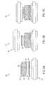
- FIG. 1depicts a diagram of a double-sided bonding structure according to one implementation of the present invention
- FIG. 2Adepicts a double-sided cooling structure without spacers according to one implementation of the present invention
- FIG. 2Bdepicts a double-sided cooling structure with spacers according to one implementation of the present invention
- FIG. 3depicts a flow diagram of a transient liquid phase (TLP) bonding process according to one implementation of the present invention
- FIGS. 4A and 4Bdepict cross-sectional views of a transition from a multiple alloy bondline to a single alloy bondline according to one implementation of the present invention
- FIGS. 5A-5Cdepict cross-sectional views of a sequential double-sided bonding process according to one implementation of the present invention
- FIGS. 6A-6Ddepict cross-sectional views of a sequential double-sided bonding process according to one implementation of the present invention.
- FIG. 7depicts a diagram of a process profile of the sequential double-sided bonding process of FIG. 6 according to one implementation of the present invention
- FIGS. 8A-8Cdepict cross-sectional views of a sequential double-sided bonding process using different thicknesses of bonding material according to one implementation of the present invention
- FIGS. 9A-9Ddepict cross-sectional views of a simultaneous double-sided bonding process according to one implementation of the present invention.
- FIG. 10depicts a diagram of a process profile of the sequential double-sided bonding process of FIG. 9 according to one implementation of the present invention.
- the present inventionis generally directed to an improved bonding via transient liquid phase bonding in power electronics.
- Transient liquid phase (TLP) bondingproduces joints that have microstructural and hence mechanical properties different to those properties of the base materials.
- TLP bondingdiffers from solder bonding in which diffusion occurs when a melting point depressant element from an interlayer moves into lattice and grain boundaries of the substrates at the bonding temperature.
- Solid state diffusional processeslead to a change of composition at the bond interface and one parent material has a low melting temperature, which melts and works as an interlayer, and another parent material with a high melting temperature.
- a thin layer of liquidspreads along the interface to form a joint at a lower temperature than the melting point of the parent material with the high melting temperature.
- a reduction in bonding temperatureleads to solidification of the melt, and this phase can subsequently be diffused away into the parent materials by holding at bonding temperature.
- Double-sided bondingcan produce advanced power modules and other electronic devices. Double-sided bonding refers to a technique where components are attached to both the top and bottom sides of an electronic device.
- FIG. 1depicts a double-sided bonding structure 100 including a device 110 .
- the device 110has a top side 112 , upon which a top metal layer 120 is disposed.
- the device 110also has a bottom side 114 , upon which a bottom metal layer 130 is disposed.
- a top-side bonding material 140bonds a top-side bonding objective 160 to the top side 112 .
- a bottom-side bonding materialbonds a bottom-side bonding objective 170 to the bottom side 114 .
- a simultaneous bonding process with solderis used for double-sided bonding.
- the top-side bonding material 140 and the bottom-side bonding material 150are the same solder.
- the solderis applied to both the top side 112 and the bottom side 114 , and the top-side bonding objective 160 and the bottom-side bonding objective 170 are respectively placed on the top side 112 and the bottom side 114 .
- the double-sided bonding structure 100undergoes processing to activate the solder.
- both sidescannot be reliably soldered at the same time because of reflow and other misalignment issues and fine process control considerations.
- Soldermay be used in sequential bonding processes as well, though not as common as simultaneous bonding.
- the top-side bonding material 140 and the bottom-side bonding material 150are solders having different melting temperatures.
- the device 110is placed in a fixture (not shown) to bond a first side. Throughout this disclosure, the bottom side will be described as being bonded first. However, the top side may be bonded first instead such that either the bottom side or the top side may be the first side, and the opposite side being the second side.
- the bottom side 114is soldered to the bottom-side bonding objective 170 .
- the device 110is inspected for alignment of the bottom-side bonding objective 170 before bonding the second side, because the top-side bonding objective 160 can obscure or prevent inspection of the alignment of the bottom side 114 .
- the device 110may be removed from the fixture for inspection before being placed back into the fixture to solder the top side 112 .
- the top-side bonding material 140 and the bottom-side bonding material 150are different solders, because the pre-bonding on the bottom side (first side) would melt and be damaged during the bonding of the top side (second side).
- FIGS. 2A and 2Bshow examples of double-sided bonding structures.
- FIG. 2Adepicts a double-sided bonding structure 200 .
- dies 210which may be insulated-gate bipolar transistors (IGBT), metal-oxide-semiconductor field-effect transistors (MOSFET), junction gate field-effect transistors (JFET), diodes, or other electronic component, are double-sided bonded through a die attach 215 to insulated substrates 220 , which may be direct bonded copper (DBC), direct bonded aluminum (DBA), or active metal brazing (AMB) substrates.
- the substrates 220are further connected through a cooler attach 225 to cold plates 230 .
- FIG. 2Billustrates a double-sided bonding structure 250 having spacers 263 .
- dies 260which may be an IGBT, MOSFET, JFET, a diode, or other electronic component, are connected through a solder 265 to a collector plate 280 on the bottom side.
- the dies 260are soldered to the spacers 263 , which are further soldered to an emitter plate 270 .
- TLP bondingcan be applied to double-sided bonding, for example, by replacing the soldering process. As stated above, TLP bonding has a higher re-melting temperature than soldering. Unlike soldering, TLP further provides the option of simultaneous or sequential bonding. The bonding material and its thickness may be selected to suit the application. TLP further allows bonding to various types of materials, such as spacers made of different materials than the device.
- FIG. 3depicts a system and method 300 utilizing TLP bonding.
- TLP bondingmay be effective for high power semiconductor devices because the re-melting temperature (i.e., sustainable temperature) is significantly larger than the bonding temperature or diffusion/solidification temperature.
- TLPmay be useful in many electronic devices, especially for high temperature power electronic devices, such as those made of silicon, SiC, GaN, etc.
- TLPAn overview of TLP is illustrated in FIG. 3 .
- two (or multiple) materialsare involved with TLP bonding.
- material A 310that has a high melting temperature
- material B 320that has a low melting temperature with respect to the melting temperature of material A 310
- both the material A 310 and the material B 320center material
- bonding temperatureincreases, the material B 320 begins to melt and diffuse into the material A 310 , as shown at step 2 of FIG. 3 .
- the diffused materialsmay sequentially react with the material B 320 and form an alloy via isothermal solidification.
- the solidificationmay continue until the bondline becomes a complete set of A+B alloy, such as depicted in step 4 of FIG. 3 (e.g., homogeneous bondline).
- Mechanical pressure(such as the range of several kPa to several MPa, such as from 3 kPa to 1 MPa) may be applied during the TLP bonding process.
- multiple A+B alloysmay generate multiple compounds such as depicted in step 5 of FIG. 3 leading to the non-homogeneous bondline.
- This non-homogenous bondlineis often considered to be non-ideal because of its non-uniformity, inconsistency, uncontrollability, and unpredictable quality, which may present problems for production.
- copper-tin (Cu—Sn)are TLP materials that may generate multiple Cu—Sn compounds (or alloys).
- the methods 300 of this disclosureare configured to minimize the non-homogeneous bondline generation.
- a particular alloy of the multiple available alloysmay be more suitable for power electronics applications, due to the high power usage and high temperature generation of the power electronics, such as a conductive bondline.
- the Cu 3 Sn alloyhas a higher electrical conductivity as compared to Cu 6 Sn 5 , even though both alloys are generated during the Cu—Sn TLP bonding process (Cu 3 Sn corresponds to alloy B+ and Cu 6 Sn 5 corresponds to alloy A+).
- a targetmay be to utilize a process to create a homogeneous bondline made of the preferred material (e.g., Cu 3 Sn alloy instead of Cu 6 Sn 5 ).
- table 1 belowillustrates a non-exhaustive list of additional bonding materials.
- the method 300may be utilized to achieve a homogeneous bondline made of a single alloy.
- a single alloymay be achieved based on attributes targeted to power electronics applications.
- One example alloyis Cu 3 Sn which is more suitable in power electronics compared to other alloys, such as Cu 6 Sn 5 .
- the method 300may be configured to fabricate a thick bondline, which is advantageous in reducing bondline stress induced by high temperature. Also, aiding in mass production, the present system does not require long bonding time and is less depend on fabrication conditions. For instance, the bonding process of the method 300 is between about 30 minutes to about 2 hours.
- the method 300provides excellent contact and good electrical and thermal conductivity to bonded devices, and therefore, improves device performance as well as bonding quality over prior techniques.
- FIGS. 4A and 4Bdepict cross-sectional views of a transition from a multiple alloy bondline to a single alloy bondline.
- the bonding processmay be complete because material B has transformed to a first alloy 410 , an A+B alloy.
- the first alloy 410is generally sandwiched between two layers of a second alloy 420 , as the diffusion has not completed, similar to step 5 of FIG. 3 .
- the bondline in the bonding state 400is not homogeneous, the non-homogenous bondline produces a suitable bond.
- the materialhas substantially diffused such that the two materials now form a single alloy, the second alloy 420 .
- the homogeneous bondline of the bonding state 450may provide a stronger bond than the non-homogeneous bondline of FIG. 4A .
- FIGS. 5A-5Cdepict a sequential double-sided bonding process 500 using TLP bonding.
- a device 510has a top side 512 upon which a top-side metal layer 520 is disposed, and a bottom side 514 upon which a bottom-side metal layer 530 is disposed.
- the top-side metal layer 520 and the bottom-side metal layer 530may comprise the same or different metal or metal alloy, or may comprise more than one metal, such as a thin gold layer over another metal.
- a bottom-side bonding material 550which may be a suitable TLP material such as a first material sandwiched between two layers of a second material as described above, is applied between the bottom-side metal layer 530 and a bottom-side bonding objective.
- the bottom side 514is then processed such that the first bonding is complete (i.e., the first material forms an alloy as in steps 4 or 5 in FIG. 3 ).
- a top-side bonding material 540which may be a suitable TLP material as described above, is applied between the top-side metal layer 520 and a top-side bonding objective 560 .
- the second bondingis complete, completing the double-sided bonding.
- the present inventiontakes advantage of the higher re-melting temperature with respect to the process temperature to share the thermal budget from the second bonding to complete the first bonding.
- the concept of sharing the thermal budgetis applicable to both the case when the same TLP material combination is used and the case when different TLP material combinations (or thicknesses) are used.
- the devicemay be an electronic device such as a power module or other semiconductor device, such as IGBTs, MOSFETs, JFETs, diodes, etc.
- the metal layersmay be one or more metals, in separate layers or an alloy, which may be electrically and/or thermally conductive.
- the metal layersmay be plated with a thin layer of another metal, such as gold.
- the bonding objectivesmay be additional electronic devices or components, or alternatively be cooling devices.
- the bonding materialmay be a combination of materials suitable for TLP, such as the material combinations of Table 1.
- FIGS. 6A-6Dillustrates a sequential double-sided bonding process 600 , wherein the same TLP material combination is used for both sides.
- a device 610has a top side 612 , upon which a top-side metal layer 620 is disposed, and a bottom side 614 , upon which a bottom-side metal layer 630 is disposed.
- a bottom-side bonding material 650for example, a suitable TLP material, is applied between the bottom-side metal layer 630 and a bottom-side bonding objective 670 .
- the first bondingis not complete, as shown by a partially completed bottom-side bonding material 655 in FIG. 6D .
- the partially completed bottom-side bonding material 655is not completely bonded, comprising one alloy and a parent material rather than two alloys, as in FIG. 4A .
- the first bonding processis stopped before the transformation of the bottom-side bonding material 650 is complete.
- the top-side bonding processis conducted.
- a top-side bonding material 640the same material as the bottom-side bonding material 650 , is applied between the top-side metal layer 620 and a top-side bonding objective 660 .
- both the bottom-side bonding material 650 and the top-side bonding material 640are completely bonded as a result of the second bonding process. Because the second bonding is the same process as the first bonding, the partially completed bottom-side bonding material 655 re-starts its melting, diffusion, and solidification process during the second bonding process. The second bonding also completes the transformation of the top-side bonding material 640 .
- this sequential processdecreases the total bonding time needed.
- a homogeneous bondlinemay be formed when the bonding processes are complete, in other implementations, the bonding processes may end with a non-homogeneous bondline.
- FIG. 7depicts a process profile 700 of the double-sided bonding process 600 .
- the process profile 700represents a conceptual diagram and is not drawn to scale.
- the first bonding processstarts with raising the temperature to a melting temperature 710 for a time period 740 .
- the temperatureis raised to a first solidification temperature 720 for a time period 745 .
- the first solidification temperatureis not maintained for a long enough time to completely transform (i.e., diffuse and solidify) the bottom-side bonding material 650 , resulting in the partially completed bottom-side bonding material 655 .
- the temperatureis reduced. Although the partially completed bottom-side bonding material 655 is not completely transformed, enough material has melted and diffused to create a bond.
- the device 610may optionally be removed to check for alignment.
- the device 610may be returned to the fixture to start the second bonding process.
- the temperatureis again raised to the melting temperature 710 because the top-side bonding material 640 is the same as the bottom-side bonding material 650 , i.e., the same processing temperatures may be used.
- the melting temperature 710is maintained for a time period 750 . During this time, the partially completed bottom-side bonding material 655 is not damaged, but rather continues its melting process.
- the temperatureis raised to a diffusion/solidification temperature 730 , referred to as the second solidification temperature 730 .
- the second solidification temperature 730is held for a time period 760 , which is sufficient for the partially completed bottom-side bonding material 655 and the top-side bonding material 640 to completely transform. Because the time period 760 is not repeated (i.e., the time period 745 is less than the time period 760 ), the total processing time is greatly reduced.
- a sequential double-sided bonding process 800 in FIGS. 8A-8Cillustrates one implementation wherein one side (the bottom side, although in other implementations the top side) requires a thicker bonding thickness than the other side.
- a device 810has a top side 812 , upon which a top-side metal layer 820 is disposed, and a bottom side 814 , upon which a bottom-side metal layer 830 is disposed.
- a bottom-side bonding material 850is applied between the bottom-side metal layer 830 and a bottom-side bonding objective 870 .
- the bottom-side bonding material 850is thicker than a top-side bonding material 840 applied between the top-side metal layer 820 and a top-side bonding objective 860 .
- the first bonding processstarts in FIG. 8A , similar to FIG. 6A .
- the first bonding timeis adjusted to make the amount of the left-over or untransformed center material in a partially completed bottom-side bonding material 855 (i.e., material B in FIG. 3 ) to be smaller than the amount of center material (i.e., material B in FIG. 3 ) in the top-side bonding material 840 , as seen in FIG. 8B .
- FIGS. 9A-9Ddepict a simultaneous double-sided bonding process 900 .
- a device 910has a top side 912 , upon which a top-side metal layer 920 is disposed, and a bottom side 914 , upon which a bottom-side metal layer 930 is disposed.
- both a top-side bonding objective 960 and a bottom-side bonding objective 970are aligned over a top-side bonding material 940 and a bottom-side bonding material 950 , respectively.
- the bottom-side bonding material 950has a lower bonding temperature than the top-side bonding material 940 , although in other implementations this may be reversed.
- FIG. 10illustrates a process profile 1000 of the simultaneous double-sided bonding TLP process 900 .
- the process profile 1000is not drawn to scale.
- the temperatureis raised to a melting temperature 1010 (the lower temperature) of the bottom-side bonding material 950 (in particular the center material) for a time period 1040 .
- the melting temperature 1010is maintained until the center material of the bottom-side bonding material 950 and the center material of the top-side bonding material 940 are completely melted.
- the temperatureis then raised to a first solidification temperature 1020 , which is the diffusion/solidification temperature of the bottom-side bonding material 950 , the first material.
- the first solidification temperature 1020is held for a time period 1050 , which allows the bottom-side bonding material 950 to diffuse and react.
- the first bondingis not completed before starting the second bonding process, as indicated by the partially completed bottom-side bonding material 955 .
- the temperatureis raised to a second solidification temperature 1030 , which is the diffusion/solidification temperature of the top-side bonding material 940 .
- the second solidification temperature 1030is maintained for a time period 1060 , which is sufficient time to complete the first and second bonding processes, as seen in FIG. 9C .
- FIG. 10lacks the time period 745 for a first partial solidification, and the time period 770 between bonding processes. Further, since the first bonding process utilizes the thermal energy of the second bonding process, the total processing time is reduced. The increased temperature of the second bonding process further increases the diffusion and reaction speed of the first bonding process. Thus, the simultaneous double-sided bonding process may improve processing times over the sequential double-sided bonding process.
- the advantages of the present inventioninclude, but are not limited to, customizability to choose between a sequential or simultaneous bonding process, greatly reducing bonding time without the introduction of new materials, structure, or processes (particularly advantageous for mass production), less dependent on fabrication conditions and no requirement for long bonding times (also important for mass production), providing excellent contact and good electrical and thermal conductivity to bonded devices, which secures device performance as well as bonding quality, the option to use different materials or conduct pre-treatment of material surfaces, enabling flexible fabrication process design and applicable to many applications, and compatibility with conventional fabrication techniques.
- a software modulemay reside in RAM memory, flash memory, ROM memory, EPROM memory, EEPROM memory, registers, hard disk, a removable disk, a CD-ROM, or any other form of storage medium known in the art.
- An exemplary storage mediumis coupled to the processor such that the processor can read information from, and write information to, the storage medium.
- the storage mediummay be integral to the processor.
- the processor and the storage mediummay reside in an Application Specific Integrated Circuit (ASIC).
- ASICApplication Specific Integrated Circuit
Landscapes
- Engineering & Computer Science (AREA)
- Mechanical Engineering (AREA)
- Microelectronics & Electronic Packaging (AREA)
- Computer Hardware Design (AREA)
- Power Engineering (AREA)
- Manufacturing & Machinery (AREA)
- Die Bonding (AREA)
Abstract
Description
| TABLE 1 | ||||
| Material System | Bonding Process | Remelt Temp. | ||
| Copper- | 4 min at 280° C. | >415° C. | ||
| Silver-Tin | 60 min at 250° C. | >600° C. | ||
| Silver- | 120 min at 175° C. | >880° C. | ||
| Gold-Tin | 15 min at 260° C. | >278° C. | ||
| Gold-Indium | 0.5 min at 200° C. | >495° C. | ||
| Nickel-Tin | 6 min at 300° C. | >400° C. | ||
Claims (20)
Priority Applications (2)
| Application Number | Priority Date | Filing Date | Title |
|---|---|---|---|
| US13/957,320US9044822B2 (en) | 2012-04-17 | 2013-08-01 | Transient liquid phase bonding process for double sided power modules |
| JP2014137682AJP6374240B2 (en) | 2013-07-05 | 2014-07-03 | Liquid phase diffusion bonding process for double-sided power modules |
Applications Claiming Priority (3)
| Application Number | Priority Date | Filing Date | Title |
|---|---|---|---|
| US13/448,632US10058951B2 (en) | 2012-04-17 | 2012-04-17 | Alloy formation control of transient liquid phase bonding |
| US201361843296P | 2013-07-05 | 2013-07-05 | |
| US13/957,320US9044822B2 (en) | 2012-04-17 | 2013-08-01 | Transient liquid phase bonding process for double sided power modules |
Publications (2)
| Publication Number | Publication Date |
|---|---|
| US20150008253A1 US20150008253A1 (en) | 2015-01-08 |
| US9044822B2true US9044822B2 (en) | 2015-06-02 |
Family
ID=52132116
Family Applications (1)
| Application Number | Title | Priority Date | Filing Date |
|---|---|---|---|
| US13/957,320Active2034-01-03US9044822B2 (en) | 2012-04-17 | 2013-08-01 | Transient liquid phase bonding process for double sided power modules |
Country Status (1)
| Country | Link |
|---|---|
| US (1) | US9044822B2 (en) |
Cited By (2)
| Publication number | Priority date | Publication date | Assignee | Title |
|---|---|---|---|---|
| US10403594B2 (en) | 2018-01-22 | 2019-09-03 | Toyota Motor Engineering & Manufacturing North America, Inc. | Hybrid bonding materials comprising ball grid arrays and metal inverse opal bonding layers, and power electronics assemblies incorporating the same |
| US20230197674A1 (en)* | 2020-09-14 | 2023-06-22 | Infineon Technologies Austria Ag | Diffusion Soldering with Contaminant Protection |
Families Citing this family (19)
| Publication number | Priority date | Publication date | Assignee | Title |
|---|---|---|---|---|
| TWI661494B (en) | 2014-07-31 | 2019-06-01 | 美商西凱渥資訊處理科技公司 | Multilayered transient liquid phase bonding |
| US10541152B2 (en) | 2014-07-31 | 2020-01-21 | Skyworks Solutions, Inc. | Transient liquid phase material bonding and sealing structures and methods of forming same |
| KR102311677B1 (en)* | 2014-08-13 | 2021-10-12 | 삼성전자주식회사 | Semiconductor device and method of manufacturing the same |
| KR20160049786A (en)* | 2014-10-28 | 2016-05-10 | 현대모비스 주식회사 | Power module and pakaking method thereof |
| US9909197B2 (en)* | 2014-12-22 | 2018-03-06 | Semes Co., Ltd. | Supporting unit and substrate treating apparatus including the same |
| US10500661B2 (en) | 2015-11-06 | 2019-12-10 | Toyota Motor Engineering & Manufacturing North America, Inc. | Methods and apparatuses for high temperature bonding controlled processing and bonded substrates formed therefrom |
| WO2017100256A1 (en)* | 2015-12-08 | 2017-06-15 | Skyworks Solutions, Inc. | Transient liquid phase material bonding and sealing structures and methods of forming same |
| JP6721329B2 (en) | 2015-12-21 | 2020-07-15 | 三菱電機株式会社 | Power semiconductor device and manufacturing method thereof |
| DE102016119485A1 (en) | 2016-10-12 | 2018-04-12 | Infineon Technologies Ag | A chip carrier having an electrically conductive layer that extends beyond a thermally conductive dielectric sheet structure |
| JP2018113678A (en) | 2016-12-02 | 2018-07-19 | スカイワークス ソリューションズ, インコーポレイテッドSkyworks Solutions, Inc. | Electronic device including vias formed in cavities between substrates |
| US10886251B2 (en)* | 2017-04-21 | 2021-01-05 | Toyota Motor Engineering & Manufacturing North America, Inc. | Multi-layered composite bonding materials and power electronics assemblies incorporating the same |
| US20190078212A1 (en)* | 2017-09-11 | 2019-03-14 | Toyota Motor Engineering & Manufacturing North America, Inc. | Transient liquid phase bonding compositions and power electronics assemblies incorporating the same |
| KR102496483B1 (en) | 2017-11-23 | 2023-02-06 | 삼성전자주식회사 | Avalanche photodetector and image sensor including the same |
| US10381223B2 (en)* | 2017-11-28 | 2019-08-13 | Toyota Motor Engineering & Manufacturing North America, Inc. | Multilayer composite bonding materials and power electronics assemblies incorporating the same |
| FR3078497B1 (en)* | 2018-03-05 | 2020-03-13 | Irt Saint Exupery | BRAZING CREAM, METHOD FOR PREPARING SUCH A BRAZING CREAM AND BRAZING METHOD USING THE SAME |
| DE102019108443A1 (en)* | 2019-04-01 | 2020-10-01 | Infineon Technologies Ag | Power semiconductor module and method for manufacturing a power semiconductor module |
| JP7657780B2 (en)* | 2019-09-12 | 2025-04-07 | ワットロー・エレクトリック・マニュファクチャリング・カンパニー | Ceramic heater and method for forming using liquid phase diffusion bonding |
| US20230317670A1 (en)* | 2022-03-29 | 2023-10-05 | Wolfspeed, Inc. | Packaged electronic devices having transient liquid phase solder joints and methods of forming same |
| DE102023131877A1 (en)* | 2023-11-15 | 2025-05-15 | TRUMPF Hüttinger GmbH + Co. KG | Power electronic unit with cooling and power converter |
Citations (120)
| Publication number | Priority date | Publication date | Assignee | Title |
|---|---|---|---|---|
| US4551904A (en) | 1982-02-09 | 1985-11-12 | Trw Inc. | Opposed gate-source transistor |
| US5113145A (en) | 1990-03-09 | 1992-05-12 | Siemens Aktiengesellschaft | Power amplifier for feeding an inductance with switched transistors |
| US5152695A (en) | 1991-10-10 | 1992-10-06 | Amp Incorporated | Surface mount electrical connector |
| US5166774A (en) | 1990-10-05 | 1992-11-24 | Motorola, Inc. | Selectively releasing conductive runner and substrate assembly having non-planar areas |
| US5225633A (en) | 1991-10-04 | 1993-07-06 | The United States Of America As Represented By The Secretary Of The Air Force | Bridge chip interconnect system |
| US5234152A (en) | 1992-01-07 | 1993-08-10 | Regents Of The University Of California | Transient liquid phase ceramic bonding |
| US5280139A (en) | 1990-03-01 | 1994-01-18 | Motorola, Inc. | Selectively releasing conductive runner and substrate assembly |
| US5289967A (en) | 1991-03-07 | 1994-03-01 | Rockwell International Corporation | Synthesis of metal matrix composites by transient liquid consolidation |
| US5372298A (en)* | 1992-01-07 | 1994-12-13 | The Regents Of The University Of California | Transient liquid phase ceramic bonding |
| US5381944A (en) | 1993-11-04 | 1995-01-17 | The Regents Of The University Of California | Low temperature reactive bonding |
| US5402926A (en) | 1992-10-01 | 1995-04-04 | Ngk Insulators, Ltd. | Brazing method using patterned metallic film having high wettability with respect to low-wettability brazing metal between components to be bonded together |
| US5416429A (en) | 1994-05-23 | 1995-05-16 | Wentworth Laboratories, Inc. | Probe assembly for testing integrated circuits |
| US5432998A (en) | 1993-07-27 | 1995-07-18 | International Business Machines, Corporation | Method of solder bonding processor package |
| US5542602A (en) | 1994-12-30 | 1996-08-06 | International Business Machines Corporation | Stabilization of conductive adhesive by metallurgical bonding |
| US5613861A (en) | 1995-06-07 | 1997-03-25 | Xerox Corporation | Photolithographically patterned spring contact |
| US5821827A (en) | 1996-12-18 | 1998-10-13 | Endgate Corporation | Coplanar oscillator circuit structures |
| US5830289A (en) | 1996-02-01 | 1998-11-03 | Boeing North American, Inc. | Process for enhancing the bond strength of resistance welded joints between titanium alloy articles |
| US5836075A (en) | 1996-12-31 | 1998-11-17 | Westinghouse Electric Corporation | Process for forming combustion turbine components by transient liquid phase bonding |
| US5847572A (en) | 1996-01-10 | 1998-12-08 | Mitsubishi Denki Kabushiki Kaisha | Partly replaceable device for testing a multi-contact integrated circuit chip package |
| US5910341A (en) | 1996-10-31 | 1999-06-08 | International Business Machines Corporation | Method of controlling the spread of an adhesive on a circuitized organic substrate |
| US5935430A (en) | 1997-04-30 | 1999-08-10 | Hewlett-Packard Company | Structure for capturing express transient liquid phase during diffusion bonding of planar devices |
| US5997708A (en) | 1997-04-30 | 1999-12-07 | Hewlett-Packard Company | Multilayer integrated assembly having specialized intermediary substrate |
| US6098871A (en) | 1997-07-22 | 2000-08-08 | United Technologies Corporation | Process for bonding metallic members using localized rapid heating |
| US6199751B1 (en) | 1998-05-28 | 2001-03-13 | International Business Machines Corporation | Polymer with transient liquid phase bondable particles |
| US6257481B1 (en) | 1997-05-06 | 2001-07-10 | Cambridge University Technical Services Limited | Metal bonding |
| US6303992B1 (en) | 1999-07-06 | 2001-10-16 | Visteon Global Technologies, Inc. | Interposer for mounting semiconductor dice on substrates |
| US6330164B1 (en) | 1985-10-18 | 2001-12-11 | Formfactor, Inc. | Interconnect assemblies and methods including ancillary electronic component connected in immediate proximity of semiconductor device |
| US20020092895A1 (en) | 2001-01-12 | 2002-07-18 | Edmund Blackshear | Formation of a solder joint having a transient liquid phase by annealing and quenching |
| US20020110008A1 (en) | 2000-01-31 | 2002-08-15 | Hideki Miyazaki | Method and apparatus for driving a semiconductor element with variable resistance circuitry |
| US6444921B1 (en) | 2000-02-03 | 2002-09-03 | Fujitsu Limited | Reduced stress and zero stress interposers for integrated-circuit chips, multichip substrates, and the like |
| US20020148880A1 (en)* | 2001-04-17 | 2002-10-17 | Damon Brink | Metal laminate structure and method for making |
| US6529022B2 (en) | 2000-12-15 | 2003-03-04 | Eaglestone Pareners I, Llc | Wafer testing interposer for a conventional package |
| US20030099097A1 (en) | 2001-11-27 | 2003-05-29 | Sammy Mok | Construction structures and manufacturing processes for probe card assemblies and packages having wafer level springs |
| US20030127495A1 (en)* | 2002-01-07 | 2003-07-10 | International Business Machines Corporation | Method of forming metallic z-interconnects for laminate chip packages and boards |
| US6602053B2 (en) | 2001-08-02 | 2003-08-05 | Siemens Westinghouse Power Corporation | Cooling structure and method of manufacturing the same |
| US20030173499A1 (en) | 2002-03-18 | 2003-09-18 | Honeywell International Inc. | Multi-substrate package assembly |
| US6624484B2 (en) | 2001-07-31 | 2003-09-23 | Nokia Corporation | IGFET and tuning circuit |
| US6669489B1 (en) | 1993-11-16 | 2003-12-30 | Formfactor, Inc. | Interposer, socket and assembly for socketing an electronic component and method of making and using same |
| US20040058470A1 (en) | 2001-08-29 | 2004-03-25 | Canella Robert L. | Methods of forming a contact array in situ on a substrate and resulting substrate assemblies |
| JP2004165186A (en) | 2002-11-08 | 2004-06-10 | Matsushita Electric Works Ltd | Resin supply method and system thereof |
| US6772501B2 (en)* | 2001-07-23 | 2004-08-10 | Itn Energy Systems, Inc. | Apparatus and method for the design and manufacture of thin-film electrochemical devices |
| US6790684B2 (en) | 2000-08-17 | 2004-09-14 | Micron Technology, Inc. | Wafer on wafer packaging and method of fabrication for full-wafer burn-in and testing |
| US20040183207A1 (en) | 2001-12-26 | 2004-09-23 | Jeung Boon Suan | Multi-substrate microelectronic packages and methods for manufacture |
| US6836011B2 (en) | 2001-09-07 | 2004-12-28 | Nec Electronics Corporation | Semiconductor chip mounting structure with movable connection electrodes |
| US20040262742A1 (en) | 1994-07-07 | 2004-12-30 | Tessera, Inc. | Semiconductor package with heat sink |
| US20050011937A1 (en)* | 2003-07-16 | 2005-01-20 | Damon Brink | Metal laminate structure and method for making |
| US6845901B2 (en) | 2002-08-22 | 2005-01-25 | Micron Technology, Inc. | Apparatus and method for depositing and reflowing solder paste on a microelectronic workpiece |
| US20050026351A1 (en) | 1999-08-25 | 2005-02-03 | Micron Technology, Inc. | Packaging of electronic chips with air-bridge structures |
| US20050035347A1 (en) | 1993-11-16 | 2005-02-17 | Khandros Igor Y. | Probe card assembly |
| US6864588B2 (en) | 2003-01-14 | 2005-03-08 | Advanced Semiconductor Engineering Inc. | MCM package with bridge connection |
| US6937037B2 (en) | 1995-11-09 | 2005-08-30 | Formfactor, Et Al. | Probe card assembly for contacting a device with raised contact elements |
| US6958531B2 (en) | 2003-11-14 | 2005-10-25 | The Regents Of The University Of Michigan | Multi-substrate package and method for assembling same |
| US20050257877A1 (en) | 2004-04-19 | 2005-11-24 | Stark David H | Bonded assemblies |
| US6975518B2 (en) | 2001-06-29 | 2005-12-13 | Intel Corporation | Printed circuit board housing clamp |
| US6992520B1 (en) | 2002-01-22 | 2006-01-31 | Edward Herbert | Gate drive method and apparatus for reducing losses in the switching of MOSFETs |
| US7002249B2 (en) | 2002-11-12 | 2006-02-21 | Primarion, Inc. | Microelectronic component with reduced parasitic inductance and method of fabricating |
| CA2513914A1 (en)* | 2004-10-04 | 2006-04-04 | United Technologies Corporation | Transient liquid phase bonding using sandwich interlayers |
| US20060283921A1 (en)* | 2005-06-15 | 2006-12-21 | Siemens Westinghouse Power Corporation | Method of diffusion bonding of nickel based superalloy substrates |
| US7165712B2 (en) | 2003-10-23 | 2007-01-23 | Siemens Power Generation, Inc. | Transient liquid phase bonding to cold-worked surfaces |
| US20070075422A1 (en) | 2004-08-11 | 2007-04-05 | Sadamasa Fujii | Electronic device, semiconductor device using same, and method for manufacturing semiconductor device |
| US20070144841A1 (en) | 2001-11-21 | 2007-06-28 | Chong Fu C | Miniaturized Contact Spring |
| US20070152026A1 (en) | 2005-12-30 | 2007-07-05 | Daewoong Suh | Transient liquid phase bonding method |
| US7245137B2 (en) | 2000-11-09 | 2007-07-17 | Formfactor, Inc. | Test head assembly having paired contact structures |
| JP2007189154A (en) | 2006-01-16 | 2007-07-26 | Fujitsu Ltd | Thermal conductive bonding material and mounting method |
| US7259625B2 (en) | 2005-04-05 | 2007-08-21 | International Business Machines Corporation | High Q monolithic inductors for use in differential circuits |
| US7279788B2 (en) | 2001-08-21 | 2007-10-09 | Micron Technology, Inc. | Device for establishing non-permanent electrical connection between an integrated circuit device lead element and a substrate |
| JP2007287927A (en) | 2006-04-17 | 2007-11-01 | Matsushita Electric Ind Co Ltd | IC component mounting method, die bonding apparatus and electronic component |
| US20070259539A1 (en) | 2003-04-11 | 2007-11-08 | Brown Dirk D | Method and system for batch manufacturing of spring elements |
| US7297989B2 (en) | 2002-08-26 | 2007-11-20 | National Institute For Materials Science | Diboride single crystal substrate, semiconductor device using this and its manufacturing method |
| US7301358B2 (en) | 2002-07-16 | 2007-11-27 | Aehr Test Systems | Contactor assembly for testing electrical circuits |
| US20080003777A1 (en) | 2006-06-30 | 2008-01-03 | Slater David B | Nickel Tin Bonding System for Semiconductor Wafers and Devices |
| US7335931B2 (en) | 2004-12-17 | 2008-02-26 | Raytheon Company | Monolithic microwave integrated circuit compatible FET structure |
| US20080061808A1 (en) | 2006-09-12 | 2008-03-13 | Sammy Mok | Compliance partitioning in testing of integrated circuits |
| US20080073665A1 (en) | 2006-09-22 | 2008-03-27 | Slater David B | Modified Gold-Tin System With Increased Melting Temperature for Wafer Bonding |
| US20080090429A1 (en) | 2000-06-20 | 2008-04-17 | Sammy Mok | Systems for testing and packaging integrated circuits |
| US20080157799A1 (en) | 2006-12-28 | 2008-07-03 | Formfactor, Inc. | Resilient contact element and methods of fabrication |
| US20080156475A1 (en) | 2006-12-28 | 2008-07-03 | Daewoong Suh | Thermal interfaces in electronic systems |
| US7396236B2 (en) | 2001-03-16 | 2008-07-08 | Formfactor, Inc. | Wafer level interposer |
| US7398912B2 (en)* | 2002-12-26 | 2008-07-15 | Ngk Insulators, Ltd. | Different materials bonded member and production method thereof |
| US20080185713A1 (en) | 2003-06-30 | 2008-08-07 | Intel Corporation | Heat dissipating device with preselected designed interface for thermal interface materials |
| US20080213612A1 (en) | 2006-08-15 | 2008-09-04 | David Starikov | Method of bonding solid materials |
| US20080210971A1 (en) | 2006-06-30 | 2008-09-04 | Matthew Donofrio | Nickel tin bonding system with barrier layer for semiconductor wafers and devices |
| US20080253098A1 (en) | 2007-04-13 | 2008-10-16 | Hewlett-Packard Development Company, L.P. | Damage Prevention Interposer for Electronic Package and Electronic Interconnect Structure |
| US7451907B2 (en) | 2004-08-06 | 2008-11-18 | General Motors Corporation | Roll bonding of bipolar plates |
| US20090004500A1 (en)* | 2007-06-26 | 2009-01-01 | Daewoong Suh | Multilayer preform for fast transient liquid phase bonding |
| US7495877B2 (en) | 2006-03-26 | 2009-02-24 | Alpha & Omega Semiconductor, Ltd. | Circuit configuration and method to reduce ringing in the semiconductor power switching circuits |
| US7511521B2 (en) | 2002-07-16 | 2009-03-31 | Aehr Test Systems | Assembly for electrically connecting a test component to a testing machine for testing electrical circuits on the test component |
| US20090085191A1 (en) | 2007-06-07 | 2009-04-02 | The Regents Of The University Of Michigan | Environment-Resistant Module, Micropackage And Methods Of Manufacturing Same |
| US7541681B2 (en) | 2006-05-04 | 2009-06-02 | Infineon Technologies Ag | Interconnection structure, electronic component and method of manufacturing the same |
| US20090142707A1 (en) | 2004-08-19 | 2009-06-04 | Formfactor, Inc. | Method to build a wirebond probe card in a many at a time fashion |
| US20090153165A1 (en) | 1999-05-27 | 2009-06-18 | Fu Chiung Chong | High Density Interconnect System Having Rapid Fabrication Cycle |
| US7579848B2 (en) | 2000-05-23 | 2009-08-25 | Nanonexus, Inc. | High density interconnect system for IC packages and interconnect assemblies |
| US7583101B2 (en) | 2007-01-18 | 2009-09-01 | Formfactor, Inc. | Probing structure with fine pitch probes |
| US20090242121A1 (en) | 2008-03-31 | 2009-10-01 | Daewoong Suh | Low stress, low-temperature metal-metal composite flip chip interconnect |
| US7628309B1 (en) | 2005-05-03 | 2009-12-08 | Rosemount Aerospace Inc. | Transient liquid phase eutectic bonding |
| US7659614B2 (en) | 2005-01-07 | 2010-02-09 | Vivek Mehrotra | High temperature, stable SiC device interconnects and packages having low thermal resistance |
| US20100072555A1 (en) | 2008-09-24 | 2010-03-25 | Evigia Systems, Inc. | Wafer bonding method and wafer stack formed thereby |
| JP2010134082A (en) | 2008-12-03 | 2010-06-17 | Advanced Photonics Inc | Method of mounting component and apparatus manufactured thereby |
| US20100183896A1 (en) | 2009-01-22 | 2010-07-22 | Cheng-Yi Liu | Tin-silver bonding and method thereof |
| US7867563B2 (en) | 2008-11-18 | 2011-01-11 | Panasonic Corporation | Component mounting method |
| US20110009979A1 (en) | 2004-10-01 | 2011-01-13 | The Regents Of The University Of Michigan | Manufacture of Shape-Memory Alloy Cellular Materials and Structures by Transient-Liquid Reactive Joining |
| US20110064363A1 (en)* | 2009-09-14 | 2011-03-17 | Zarlink Semiconductor Ab | Self-aligned carrier assembly for optical device supporting wafer scale methods |
| DE102009050426B3 (en) | 2009-10-22 | 2011-03-31 | Fraunhofer-Gesellschaft zur Förderung der angewandten Forschung e.V. | A method of aligning components on a carrier substrate and a method of making a carrier substrate therefor and a method of assembling a target substrate therewith. |
| US20110163445A1 (en) | 2006-09-14 | 2011-07-07 | Nirupama Chakrapani | Electronic Packages With Fine Particle Wetting and Non-Wetting Zones |
| US20110180777A1 (en) | 2008-08-21 | 2011-07-28 | International Business Machines Corporation | Method of placing a semiconducting nanostructure and semiconductor device including the semiconducting nanostructure |
| US8076696B2 (en) | 2009-10-30 | 2011-12-13 | General Electric Company | Power module assembly with reduced inductance |
| US8168490B2 (en) | 2008-12-23 | 2012-05-01 | Intersil Americas, Inc. | Co-packaging approach for power converters based on planar devices, structure and method |
| US20120112201A1 (en)* | 2010-11-09 | 2012-05-10 | Board of Trustees of the Univ. of Arkansas, acting for&on behalf of the Univ. of Arkansas,Fayetevill | High melting point soldering layer and fabrication method for the same, and semiconductor device |
| US8240545B1 (en)* | 2011-08-11 | 2012-08-14 | Western Digital (Fremont), Llc | Methods for minimizing component shift during soldering |
| US20130001782A1 (en)* | 2011-06-30 | 2013-01-03 | Rohm Co., Ltd. | Laminated high melting point soldering layer and fabrication method for the same, and semiconductor device |
| US8348139B2 (en)* | 2010-03-09 | 2013-01-08 | Indium Corporation | Composite solder alloy preform |
| US20130092948A1 (en)* | 2011-10-18 | 2013-04-18 | Rohm Co., Ltd. | Semiconductor device and fabrication method of the semiconductor device |
| US20130201631A1 (en)* | 2012-02-08 | 2013-08-08 | Crane Electronics, Inc. | Multilayer electronics assembly and method for embedding electrical circuit components within a three dimensional module |
| US20130270326A1 (en)* | 2012-04-17 | 2013-10-17 | Toyota Motor Engineering & Manufacturing North America, Inc. | Alloy formation control of transient liquid phase bonding |
| US20130335921A1 (en)* | 2009-10-22 | 2013-12-19 | Mitsubishi Materials Corporation | Substrate for power module, substrate with heat sink for power module, power module, method for producing substrate for power module, and method for producing substrate with heat sink for power module |
| US20140002952A1 (en)* | 2010-05-26 | 2014-01-02 | Kemet Electrinics Corporation | Leadless Multi-Layered Ceramic Capacitor Stacks |
| US20140177132A1 (en)* | 2010-05-26 | 2014-06-26 | Kemet Electronics Corporation | Electronic Component Termination and Assembly by Means of Transient Liquid Phase Sintering Metalurgical Bonds |
| US20140193658A1 (en)* | 2011-05-31 | 2014-07-10 | Indium Corporation | Low void solder joint for multiple reflow applications |
| US8803001B2 (en)* | 2011-06-21 | 2014-08-12 | Toyota Motor Engineering & Manufacturing North America, Inc. | Bonding area design for transient liquid phase bonding process |
| US8814030B2 (en)* | 2012-04-17 | 2014-08-26 | Toyota Motor Engineering & Manufacturing North America, Inc. | Improvements of long term bondline reliability of power electronics operating at high temperatures |
- 2013
- 2013-08-01USUS13/957,320patent/US9044822B2/enactiveActive
Patent Citations (129)
| Publication number | Priority date | Publication date | Assignee | Title |
|---|---|---|---|---|
| US4551904A (en) | 1982-02-09 | 1985-11-12 | Trw Inc. | Opposed gate-source transistor |
| US6330164B1 (en) | 1985-10-18 | 2001-12-11 | Formfactor, Inc. | Interconnect assemblies and methods including ancillary electronic component connected in immediate proximity of semiconductor device |
| US5280139A (en) | 1990-03-01 | 1994-01-18 | Motorola, Inc. | Selectively releasing conductive runner and substrate assembly |
| US5113145A (en) | 1990-03-09 | 1992-05-12 | Siemens Aktiengesellschaft | Power amplifier for feeding an inductance with switched transistors |
| US5166774A (en) | 1990-10-05 | 1992-11-24 | Motorola, Inc. | Selectively releasing conductive runner and substrate assembly having non-planar areas |
| US5289967A (en) | 1991-03-07 | 1994-03-01 | Rockwell International Corporation | Synthesis of metal matrix composites by transient liquid consolidation |
| US5225633A (en) | 1991-10-04 | 1993-07-06 | The United States Of America As Represented By The Secretary Of The Air Force | Bridge chip interconnect system |
| US5152695A (en) | 1991-10-10 | 1992-10-06 | Amp Incorporated | Surface mount electrical connector |
| US5234152A (en) | 1992-01-07 | 1993-08-10 | Regents Of The University Of California | Transient liquid phase ceramic bonding |
| US5372298A (en)* | 1992-01-07 | 1994-12-13 | The Regents Of The University Of California | Transient liquid phase ceramic bonding |
| US5402926A (en) | 1992-10-01 | 1995-04-04 | Ngk Insulators, Ltd. | Brazing method using patterned metallic film having high wettability with respect to low-wettability brazing metal between components to be bonded together |
| US5432998A (en) | 1993-07-27 | 1995-07-18 | International Business Machines, Corporation | Method of solder bonding processor package |
| US5381944A (en) | 1993-11-04 | 1995-01-17 | The Regents Of The University Of California | Low temperature reactive bonding |
| US6669489B1 (en) | 1993-11-16 | 2003-12-30 | Formfactor, Inc. | Interposer, socket and assembly for socketing an electronic component and method of making and using same |
| US20040072456A1 (en) | 1993-11-16 | 2004-04-15 | Formfactor, Inc. | Methods of removably mounting electronic components to a circuit board, and sockets formed by the methods |
| US20050035347A1 (en) | 1993-11-16 | 2005-02-17 | Khandros Igor Y. | Probe card assembly |
| US5416429A (en) | 1994-05-23 | 1995-05-16 | Wentworth Laboratories, Inc. | Probe assembly for testing integrated circuits |
| US20040262742A1 (en) | 1994-07-07 | 2004-12-30 | Tessera, Inc. | Semiconductor package with heat sink |
| US5542602A (en) | 1994-12-30 | 1996-08-06 | International Business Machines Corporation | Stabilization of conductive adhesive by metallurgical bonding |
| US5613861A (en) | 1995-06-07 | 1997-03-25 | Xerox Corporation | Photolithographically patterned spring contact |
| US6937037B2 (en) | 1995-11-09 | 2005-08-30 | Formfactor, Et Al. | Probe card assembly for contacting a device with raised contact elements |
| US5847572A (en) | 1996-01-10 | 1998-12-08 | Mitsubishi Denki Kabushiki Kaisha | Partly replaceable device for testing a multi-contact integrated circuit chip package |
| US5830289A (en) | 1996-02-01 | 1998-11-03 | Boeing North American, Inc. | Process for enhancing the bond strength of resistance welded joints between titanium alloy articles |
| US5910341A (en) | 1996-10-31 | 1999-06-08 | International Business Machines Corporation | Method of controlling the spread of an adhesive on a circuitized organic substrate |
| US5821827A (en) | 1996-12-18 | 1998-10-13 | Endgate Corporation | Coplanar oscillator circuit structures |
| US5836075A (en) | 1996-12-31 | 1998-11-17 | Westinghouse Electric Corporation | Process for forming combustion turbine components by transient liquid phase bonding |
| US5997708A (en) | 1997-04-30 | 1999-12-07 | Hewlett-Packard Company | Multilayer integrated assembly having specialized intermediary substrate |
| US5935430A (en) | 1997-04-30 | 1999-08-10 | Hewlett-Packard Company | Structure for capturing express transient liquid phase during diffusion bonding of planar devices |
| US6257481B1 (en) | 1997-05-06 | 2001-07-10 | Cambridge University Technical Services Limited | Metal bonding |
| US6098871A (en) | 1997-07-22 | 2000-08-08 | United Technologies Corporation | Process for bonding metallic members using localized rapid heating |
| US6199751B1 (en) | 1998-05-28 | 2001-03-13 | International Business Machines Corporation | Polymer with transient liquid phase bondable particles |
| US20090153165A1 (en) | 1999-05-27 | 2009-06-18 | Fu Chiung Chong | High Density Interconnect System Having Rapid Fabrication Cycle |
| US6303992B1 (en) | 1999-07-06 | 2001-10-16 | Visteon Global Technologies, Inc. | Interposer for mounting semiconductor dice on substrates |
| US20070269997A1 (en) | 1999-07-30 | 2007-11-22 | Formfactor, Inc. | Electronic components with plurality of contoured microelectronic spring contacts |
| US20050026351A1 (en) | 1999-08-25 | 2005-02-03 | Micron Technology, Inc. | Packaging of electronic chips with air-bridge structures |
| US20020110008A1 (en) | 2000-01-31 | 2002-08-15 | Hideki Miyazaki | Method and apparatus for driving a semiconductor element with variable resistance circuitry |
| US6444921B1 (en) | 2000-02-03 | 2002-09-03 | Fujitsu Limited | Reduced stress and zero stress interposers for integrated-circuit chips, multichip substrates, and the like |
| US7579848B2 (en) | 2000-05-23 | 2009-08-25 | Nanonexus, Inc. | High density interconnect system for IC packages and interconnect assemblies |
| US20080090429A1 (en) | 2000-06-20 | 2008-04-17 | Sammy Mok | Systems for testing and packaging integrated circuits |
| US6790684B2 (en) | 2000-08-17 | 2004-09-14 | Micron Technology, Inc. | Wafer on wafer packaging and method of fabrication for full-wafer burn-in and testing |
| US7245137B2 (en) | 2000-11-09 | 2007-07-17 | Formfactor, Inc. | Test head assembly having paired contact structures |
| US6529022B2 (en) | 2000-12-15 | 2003-03-04 | Eaglestone Pareners I, Llc | Wafer testing interposer for a conventional package |
| US20020092895A1 (en) | 2001-01-12 | 2002-07-18 | Edmund Blackshear | Formation of a solder joint having a transient liquid phase by annealing and quenching |
| US7396236B2 (en) | 2001-03-16 | 2008-07-08 | Formfactor, Inc. | Wafer level interposer |
| US20020148880A1 (en)* | 2001-04-17 | 2002-10-17 | Damon Brink | Metal laminate structure and method for making |
| US6975518B2 (en) | 2001-06-29 | 2005-12-13 | Intel Corporation | Printed circuit board housing clamp |
| US6772501B2 (en)* | 2001-07-23 | 2004-08-10 | Itn Energy Systems, Inc. | Apparatus and method for the design and manufacture of thin-film electrochemical devices |
| US6624484B2 (en) | 2001-07-31 | 2003-09-23 | Nokia Corporation | IGFET and tuning circuit |
| US6602053B2 (en) | 2001-08-02 | 2003-08-05 | Siemens Westinghouse Power Corporation | Cooling structure and method of manufacturing the same |
| US7279788B2 (en) | 2001-08-21 | 2007-10-09 | Micron Technology, Inc. | Device for establishing non-permanent electrical connection between an integrated circuit device lead element and a substrate |
| US20040058470A1 (en) | 2001-08-29 | 2004-03-25 | Canella Robert L. | Methods of forming a contact array in situ on a substrate and resulting substrate assemblies |
| US7049693B2 (en) | 2001-08-29 | 2006-05-23 | Micron Technology, Inc. | Electrical contact array for substrate assemblies |
| US7120999B2 (en) | 2001-08-29 | 2006-10-17 | Micron Technology, Inc. | Methods of forming a contact array in situ on a substrate |
| US6836011B2 (en) | 2001-09-07 | 2004-12-28 | Nec Electronics Corporation | Semiconductor chip mounting structure with movable connection electrodes |
| US20070144841A1 (en) | 2001-11-21 | 2007-06-28 | Chong Fu C | Miniaturized Contact Spring |
| US20030099097A1 (en) | 2001-11-27 | 2003-05-29 | Sammy Mok | Construction structures and manufacturing processes for probe card assemblies and packages having wafer level springs |
| US20040183207A1 (en) | 2001-12-26 | 2004-09-23 | Jeung Boon Suan | Multi-substrate microelectronic packages and methods for manufacture |
| US20030127495A1 (en)* | 2002-01-07 | 2003-07-10 | International Business Machines Corporation | Method of forming metallic z-interconnects for laminate chip packages and boards |
| US6992520B1 (en) | 2002-01-22 | 2006-01-31 | Edward Herbert | Gate drive method and apparatus for reducing losses in the switching of MOSFETs |
| US20030173499A1 (en) | 2002-03-18 | 2003-09-18 | Honeywell International Inc. | Multi-substrate package assembly |
| US7511521B2 (en) | 2002-07-16 | 2009-03-31 | Aehr Test Systems | Assembly for electrically connecting a test component to a testing machine for testing electrical circuits on the test component |
| US7301358B2 (en) | 2002-07-16 | 2007-11-27 | Aehr Test Systems | Contactor assembly for testing electrical circuits |
| US6845901B2 (en) | 2002-08-22 | 2005-01-25 | Micron Technology, Inc. | Apparatus and method for depositing and reflowing solder paste on a microelectronic workpiece |
| US7297989B2 (en) | 2002-08-26 | 2007-11-20 | National Institute For Materials Science | Diboride single crystal substrate, semiconductor device using this and its manufacturing method |
| JP2004165186A (en) | 2002-11-08 | 2004-06-10 | Matsushita Electric Works Ltd | Resin supply method and system thereof |
| US7002249B2 (en) | 2002-11-12 | 2006-02-21 | Primarion, Inc. | Microelectronic component with reduced parasitic inductance and method of fabricating |
| US7398912B2 (en)* | 2002-12-26 | 2008-07-15 | Ngk Insulators, Ltd. | Different materials bonded member and production method thereof |
| US6864588B2 (en) | 2003-01-14 | 2005-03-08 | Advanced Semiconductor Engineering Inc. | MCM package with bridge connection |
| US20070259539A1 (en) | 2003-04-11 | 2007-11-08 | Brown Dirk D | Method and system for batch manufacturing of spring elements |
| US7527090B2 (en) | 2003-06-30 | 2009-05-05 | Intel Corporation | Heat dissipating device with preselected designed interface for thermal interface materials |
| US20080185713A1 (en) | 2003-06-30 | 2008-08-07 | Intel Corporation | Heat dissipating device with preselected designed interface for thermal interface materials |
| US20050011937A1 (en)* | 2003-07-16 | 2005-01-20 | Damon Brink | Metal laminate structure and method for making |
| US7165712B2 (en) | 2003-10-23 | 2007-01-23 | Siemens Power Generation, Inc. | Transient liquid phase bonding to cold-worked surfaces |
| US6958531B2 (en) | 2003-11-14 | 2005-10-25 | The Regents Of The University Of Michigan | Multi-substrate package and method for assembling same |
| US20050257877A1 (en) | 2004-04-19 | 2005-11-24 | Stark David H | Bonded assemblies |
| US7451907B2 (en) | 2004-08-06 | 2008-11-18 | General Motors Corporation | Roll bonding of bipolar plates |
| US7612456B2 (en) | 2004-08-11 | 2009-11-03 | Rohm Co., Ltd. | Electronic device, semiconductor device using same, and method for manufacturing semiconductor device |
| US20070075422A1 (en) | 2004-08-11 | 2007-04-05 | Sadamasa Fujii | Electronic device, semiconductor device using same, and method for manufacturing semiconductor device |
| US20090142707A1 (en) | 2004-08-19 | 2009-06-04 | Formfactor, Inc. | Method to build a wirebond probe card in a many at a time fashion |
| US20110009979A1 (en) | 2004-10-01 | 2011-01-13 | The Regents Of The University Of Michigan | Manufacture of Shape-Memory Alloy Cellular Materials and Structures by Transient-Liquid Reactive Joining |
| CA2513914A1 (en)* | 2004-10-04 | 2006-04-04 | United Technologies Corporation | Transient liquid phase bonding using sandwich interlayers |
| US20060071056A1 (en) | 2004-10-04 | 2006-04-06 | Gopal Das | Transient liquid phase bonding using sandwich interlayers |
| US7335931B2 (en) | 2004-12-17 | 2008-02-26 | Raytheon Company | Monolithic microwave integrated circuit compatible FET structure |
| US7659614B2 (en) | 2005-01-07 | 2010-02-09 | Vivek Mehrotra | High temperature, stable SiC device interconnects and packages having low thermal resistance |
| US7259625B2 (en) | 2005-04-05 | 2007-08-21 | International Business Machines Corporation | High Q monolithic inductors for use in differential circuits |
| US7628309B1 (en) | 2005-05-03 | 2009-12-08 | Rosemount Aerospace Inc. | Transient liquid phase eutectic bonding |
| US20060283921A1 (en)* | 2005-06-15 | 2006-12-21 | Siemens Westinghouse Power Corporation | Method of diffusion bonding of nickel based superalloy substrates |
| US20070152026A1 (en) | 2005-12-30 | 2007-07-05 | Daewoong Suh | Transient liquid phase bonding method |
| JP2007189154A (en) | 2006-01-16 | 2007-07-26 | Fujitsu Ltd | Thermal conductive bonding material and mounting method |
| US7495877B2 (en) | 2006-03-26 | 2009-02-24 | Alpha & Omega Semiconductor, Ltd. | Circuit configuration and method to reduce ringing in the semiconductor power switching circuits |
| JP2007287927A (en) | 2006-04-17 | 2007-11-01 | Matsushita Electric Ind Co Ltd | IC component mounting method, die bonding apparatus and electronic component |
| US7541681B2 (en) | 2006-05-04 | 2009-06-02 | Infineon Technologies Ag | Interconnection structure, electronic component and method of manufacturing the same |
| US20080003777A1 (en) | 2006-06-30 | 2008-01-03 | Slater David B | Nickel Tin Bonding System for Semiconductor Wafers and Devices |
| US20080210971A1 (en) | 2006-06-30 | 2008-09-04 | Matthew Donofrio | Nickel tin bonding system with barrier layer for semiconductor wafers and devices |
| US20080213612A1 (en) | 2006-08-15 | 2008-09-04 | David Starikov | Method of bonding solid materials |
| US20080061808A1 (en) | 2006-09-12 | 2008-03-13 | Sammy Mok | Compliance partitioning in testing of integrated circuits |
| US20110163445A1 (en) | 2006-09-14 | 2011-07-07 | Nirupama Chakrapani | Electronic Packages With Fine Particle Wetting and Non-Wetting Zones |
| US20080073665A1 (en) | 2006-09-22 | 2008-03-27 | Slater David B | Modified Gold-Tin System With Increased Melting Temperature for Wafer Bonding |
| US20080156475A1 (en) | 2006-12-28 | 2008-07-03 | Daewoong Suh | Thermal interfaces in electronic systems |
| US20080157799A1 (en) | 2006-12-28 | 2008-07-03 | Formfactor, Inc. | Resilient contact element and methods of fabrication |
| US7583101B2 (en) | 2007-01-18 | 2009-09-01 | Formfactor, Inc. | Probing structure with fine pitch probes |
| US20080253098A1 (en) | 2007-04-13 | 2008-10-16 | Hewlett-Packard Development Company, L.P. | Damage Prevention Interposer for Electronic Package and Electronic Interconnect Structure |
| US20090085191A1 (en) | 2007-06-07 | 2009-04-02 | The Regents Of The University Of Michigan | Environment-Resistant Module, Micropackage And Methods Of Manufacturing Same |
| US20090004500A1 (en)* | 2007-06-26 | 2009-01-01 | Daewoong Suh | Multilayer preform for fast transient liquid phase bonding |
| US20090242121A1 (en) | 2008-03-31 | 2009-10-01 | Daewoong Suh | Low stress, low-temperature metal-metal composite flip chip interconnect |
| US20110180777A1 (en) | 2008-08-21 | 2011-07-28 | International Business Machines Corporation | Method of placing a semiconducting nanostructure and semiconductor device including the semiconducting nanostructure |
| US20100072555A1 (en) | 2008-09-24 | 2010-03-25 | Evigia Systems, Inc. | Wafer bonding method and wafer stack formed thereby |
| US7867563B2 (en) | 2008-11-18 | 2011-01-11 | Panasonic Corporation | Component mounting method |
| JP2010134082A (en) | 2008-12-03 | 2010-06-17 | Advanced Photonics Inc | Method of mounting component and apparatus manufactured thereby |
| US20110240717A1 (en) | 2008-12-03 | 2011-10-06 | Advanced Photonics, Inc. | Component mounting method and device manufactured using the same |
| US8168490B2 (en) | 2008-12-23 | 2012-05-01 | Intersil Americas, Inc. | Co-packaging approach for power converters based on planar devices, structure and method |
| US20100183896A1 (en) | 2009-01-22 | 2010-07-22 | Cheng-Yi Liu | Tin-silver bonding and method thereof |
| US20110064363A1 (en)* | 2009-09-14 | 2011-03-17 | Zarlink Semiconductor Ab | Self-aligned carrier assembly for optical device supporting wafer scale methods |
| DE102009050426B3 (en) | 2009-10-22 | 2011-03-31 | Fraunhofer-Gesellschaft zur Förderung der angewandten Forschung e.V. | A method of aligning components on a carrier substrate and a method of making a carrier substrate therefor and a method of assembling a target substrate therewith. |
| US20130335921A1 (en)* | 2009-10-22 | 2013-12-19 | Mitsubishi Materials Corporation | Substrate for power module, substrate with heat sink for power module, power module, method for producing substrate for power module, and method for producing substrate with heat sink for power module |
| US8076696B2 (en) | 2009-10-30 | 2011-12-13 | General Electric Company | Power module assembly with reduced inductance |
| US8348139B2 (en)* | 2010-03-09 | 2013-01-08 | Indium Corporation | Composite solder alloy preform |
| US20140177132A1 (en)* | 2010-05-26 | 2014-06-26 | Kemet Electronics Corporation | Electronic Component Termination and Assembly by Means of Transient Liquid Phase Sintering Metalurgical Bonds |
| US20140002952A1 (en)* | 2010-05-26 | 2014-01-02 | Kemet Electrinics Corporation | Leadless Multi-Layered Ceramic Capacitor Stacks |
| US20120112201A1 (en)* | 2010-11-09 | 2012-05-10 | Board of Trustees of the Univ. of Arkansas, acting for&on behalf of the Univ. of Arkansas,Fayetevill | High melting point soldering layer and fabrication method for the same, and semiconductor device |
| US20140193658A1 (en)* | 2011-05-31 | 2014-07-10 | Indium Corporation | Low void solder joint for multiple reflow applications |
| US8803001B2 (en)* | 2011-06-21 | 2014-08-12 | Toyota Motor Engineering & Manufacturing North America, Inc. | Bonding area design for transient liquid phase bonding process |
| US20130001782A1 (en)* | 2011-06-30 | 2013-01-03 | Rohm Co., Ltd. | Laminated high melting point soldering layer and fabrication method for the same, and semiconductor device |
| US8513806B2 (en)* | 2011-06-30 | 2013-08-20 | Rohm Co., Ltd. | Laminated high melting point soldering layer formed by TLP bonding and fabrication method for the same, and semiconductor device |
| US8240545B1 (en)* | 2011-08-11 | 2012-08-14 | Western Digital (Fremont), Llc | Methods for minimizing component shift during soldering |
| US20130092948A1 (en)* | 2011-10-18 | 2013-04-18 | Rohm Co., Ltd. | Semiconductor device and fabrication method of the semiconductor device |
| US20130201631A1 (en)* | 2012-02-08 | 2013-08-08 | Crane Electronics, Inc. | Multilayer electronics assembly and method for embedding electrical circuit components within a three dimensional module |
| US20130270326A1 (en)* | 2012-04-17 | 2013-10-17 | Toyota Motor Engineering & Manufacturing North America, Inc. | Alloy formation control of transient liquid phase bonding |
| US8814030B2 (en)* | 2012-04-17 | 2014-08-26 | Toyota Motor Engineering & Manufacturing North America, Inc. | Improvements of long term bondline reliability of power electronics operating at high temperatures |
Non-Patent Citations (16)
| Title |
|---|
| Bontemps et al.; "Low Profile Power Module Combined with State of the Art MOSFET Switches and SiC Diodes Allows High Frequency and Very Compact Three-Phase Sinusoidal Input Rectifiers" Proc. of the Conf. for Power Electronics, Intellectual Motion and Power Quality; 6 pages; 2007. |
| Bosco et al.; "Critical Interlayer Thickness for Transient Liquid Phase Bonding in the Cu-Sn System"; Acta Materialia 52; pp. 2965-2972; 2004. |
| Chen et al.; "Effect of Bonding Pressure on Transient Liquid Phase Bonding Joint Microstructure and Properties of T91/12Cr2MoWVTiB"; Advanced Materials Research; vols. 97-101; pp. 107-110; 2010. |
| Dodge; "Eliminating Parasitic Oscillation Between Parallel MOSFETs"; application Note APT-0402 Rev A; 6 pages, Mar. 25, 2004. |
| Farruggia et al.; "Hybrid Modules as an Alternative to Paralleled Discrete Devices"; International Symposium on Microelectornics; vol. 4587; 399-404, Oct. 9, 2001. |
| Frederikse et al.; "Thermal and Electrical Properties of Copper-tin and Nickel-tin Intermetallics"; AIP Journal of Applied Physics; vol. 72, No. 1, pp. 2879-2882; Oct. 1, 1992. |
| Grossi; "Self Assembly of Die to Wafer Using Direct Bonding Methods and Capillary Techniques," 207, 2010. |
| Guth et al.; "New Assembly and Interconnects Beyond Sintering Methods"; PCIM 2010; pp. 232-237; May 4-6, 2010. |
| Hikasa, K.; "Development of Flexible Bumped Tape Interposer"; Furukawa Review; No. 24; pp. 59-64; 2003. |
| Hille et al.: "Failure Mechanism and Improvement Potential of IGBT's Short Circuit Operation"; Proceedings of the 22nd International Symposium on Power Semiconductor Devices & ICs Hiroshima; pp. 33-36; 2010. |
| Kang et al.; "Isothermal Solidification of Cu/Sn Diffusion Couples to Form thin-Solder Joints"; Journal of Electronic Materials; vol. 31, No. 11; 2002. |
| MacDonald et al.; "Transient Liquid Phase Bonding Processes"; The Minerals, Metals & Materials Society; pp. 93-100; 1992. |
| Mustain, et al.; "Transient Liquid Phase Die Attach for High-Temperature Silicon Carbide Power Devices"; IEEE Transactions on Components and Packaging Technologies; V. 33, No. 3; pp. 563-570; Sep. 2010. |
| Rowden, et al.; "High Temperature SiC Power Module Packaging"; Proceedings of the ASME 2009 International Mechanical Engineering Congress & Exposition IMECE2009 Nov. 13-19. |
| Welch, III et al.; "Transfer of Metal MEMS Packages Using a Wafer-Level Solder Transfer Technique"; IEEE Transactions on Advanced Packaging; V. 28, No. 4; pp. 643-649; Nov. 2005. |
| Zheng et al.; "Partial Transient Liquid-Phase Bonding of Si3N4 with Ti/Cu/Ni Multi-Interlayers"; pp. 2026-2028; 1997. |
Cited By (3)
| Publication number | Priority date | Publication date | Assignee | Title |
|---|---|---|---|---|
| US10403594B2 (en) | 2018-01-22 | 2019-09-03 | Toyota Motor Engineering & Manufacturing North America, Inc. | Hybrid bonding materials comprising ball grid arrays and metal inverse opal bonding layers, and power electronics assemblies incorporating the same |
| US20230197674A1 (en)* | 2020-09-14 | 2023-06-22 | Infineon Technologies Austria Ag | Diffusion Soldering with Contaminant Protection |
| US12087723B2 (en)* | 2020-09-14 | 2024-09-10 | Infineon Technologies Austria Ag | Diffusion soldering with contaminant protection |
Also Published As
| Publication number | Publication date |
|---|---|
| US20150008253A1 (en) | 2015-01-08 |
Similar Documents
| Publication | Publication Date | Title |
|---|---|---|
| US9044822B2 (en) | Transient liquid phase bonding process for double sided power modules | |
| KR102122625B1 (en) | Power module substrate, power module substrate with heat sink, and power module with heat sink | |
| KR102220852B1 (en) | Method for manufacturing bonded body and method for manufacturing power-module substrate | |
| TWI614845B (en) | Method of producing substrate for power module | |
| TWI641300B (en) | Bonding body and power module substrate | |
| JP5403129B2 (en) | Power module substrate, power module substrate with heat sink, power module, and method for manufacturing power module substrate | |
| CN106165087B (en) | Substrate for power module, substrate with heat sink for power module, and power module with heat sink | |
| JP6041469B2 (en) | Method for forming high melting point solder layer | |
| CN107004653A (en) | The manufacture method of semiconductor device and semiconductor device | |
| TW201626519A (en) | Substrate with cooler for power modules and method for producing same | |
| CN103035601A (en) | Semiconductor device including diffusion soldered layer on sintered silver layer | |
| KR102330134B1 (en) | Process for producing united object and process for producing substrate for power module | |
| JP6935392B2 (en) | Semiconductor devices, power modules and their manufacturing methods | |
| JP6374240B2 (en) | Liquid phase diffusion bonding process for double-sided power modules | |
| JP2007250638A (en) | Cooler | |
| JP5966512B2 (en) | Manufacturing method of power module substrate with heat sink | |
| KR20180104659A (en) | Junction body, substrate for power module, method of manufacturing junction body, and method of manufacturing substrate for power module | |
| JP2014072364A (en) | Power module substrate and manufacturing method thereof | |
| JP5904257B2 (en) | Power module substrate manufacturing method | |
| JP2014039062A (en) | Substrate for power module, substrate for power module having heat sink, power module, and method for manufacturing substrate for power module | |
| EP4138119B1 (en) | Method for producing power semiconductor module and power semiconductor module | |
| JP5808295B2 (en) | module | |
| CN109075135B (en) | Bonded body, substrate for power module, method for manufacturing bonded body, and method for manufacturing substrate for power module | |
| JP2015002305A (en) | Semiconductor device |
Legal Events
| Date | Code | Title | Description |
|---|---|---|---|
| AS | Assignment | Owner name:TOYOTA MOTOR ENGINEERING & MANUFACTURING NORTH AME Free format text:ASSIGNMENT OF ASSIGNORS INTEREST;ASSIGNORS:YOON, SANG WON;KATO, TAKEHIRO;SHIOZAKI, KOJI;REEL/FRAME:030929/0166 Effective date:20130725 | |
| STCF | Information on status: patent grant | Free format text:PATENTED CASE | |
| AS | Assignment | Owner name:TOYOTA JIDOSHA KABUSHIKI KAISHA, JAPAN Free format text:ASSIGNMENT OF ASSIGNORS INTEREST;ASSIGNOR:TOYOTA MOTOR ENGINEERING & MANUFACTURING NORTH AMERICA, INC.;REEL/FRAME:035810/0970 Effective date:20150603 | |
| MAFP | Maintenance fee payment | Free format text:PAYMENT OF MAINTENANCE FEE, 4TH YEAR, LARGE ENTITY (ORIGINAL EVENT CODE: M1551); ENTITY STATUS OF PATENT OWNER: LARGE ENTITY Year of fee payment:4 | |
| AS | Assignment | Owner name:DENSO CORPORATION, JAPAN Free format text:NUNC PRO TUNC ASSIGNMENT;ASSIGNOR:TOYOTA JIDOSHA KABUSHIKI KAISHA;REEL/FRAME:060840/0673 Effective date:20220705 | |
| AS | Assignment | Owner name:DENSO CORPORATION, JAPAN Free format text:CORRECTIVE ASSIGNMENT TO CORRECT THE RECEIVING PARTY ADDRESS SHOULD BE KARIYA-CITY PREVIOUSLY RECORDED AT REEL: 060840 FRAME: 0673. ASSIGNOR(S) HEREBY CONFIRMS THE ASSIGNMENT;ASSIGNOR:TOYOTA JIDOSHA KABUSHIKI KAISHA;REEL/FRAME:061408/0107 Effective date:20220705 | |
| MAFP | Maintenance fee payment | Free format text:PAYMENT OF MAINTENANCE FEE, 8TH YEAR, LARGE ENTITY (ORIGINAL EVENT CODE: M1552); ENTITY STATUS OF PATENT OWNER: LARGE ENTITY Year of fee payment:8 |