US9043780B2 - Electronic system with system modification control mechanism and method of operation thereof - Google Patents
Electronic system with system modification control mechanism and method of operation thereofDownload PDFInfo
- Publication number
- US9043780B2 US9043780B2US13/851,928US201313851928AUS9043780B2US 9043780 B2US9043780 B2US 9043780B2US 201313851928 AUS201313851928 AUS 201313851928AUS 9043780 B2US9043780 B2US 9043780B2
- Authority
- US
- United States
- Prior art keywords
- signal
- recognizing
- unique
- trigger
- unique trigger
- Prior art date
- Legal status (The legal status is an assumption and is not a legal conclusion. Google has not performed a legal analysis and makes no representation as to the accuracy of the status listed.)
- Active, expires
Links
Images


Classifications
- G—PHYSICS
- G06—COMPUTING OR CALCULATING; COUNTING
- G06F—ELECTRIC DIGITAL DATA PROCESSING
- G06F9/00—Arrangements for program control, e.g. control units
- G06F9/06—Arrangements for program control, e.g. control units using stored programs, i.e. using an internal store of processing equipment to receive or retain programs
- G06F9/44—Arrangements for executing specific programs
- G06F9/4401—Bootstrapping
- G06F9/4411—Configuring for operating with peripheral devices; Loading of device drivers
- G—PHYSICS
- G06—COMPUTING OR CALCULATING; COUNTING
- G06F—ELECTRIC DIGITAL DATA PROCESSING
- G06F8/00—Arrangements for software engineering
- G06F8/60—Software deployment
- G06F8/65—Updates
- G—PHYSICS
- G06—COMPUTING OR CALCULATING; COUNTING
- G06F—ELECTRIC DIGITAL DATA PROCESSING
- G06F13/00—Interconnection of, or transfer of information or other signals between, memories, input/output devices or central processing units
- G06F13/38—Information transfer, e.g. on bus
- G06F13/42—Bus transfer protocol, e.g. handshake; Synchronisation
- G—PHYSICS
- G06—COMPUTING OR CALCULATING; COUNTING
- G06F—ELECTRIC DIGITAL DATA PROCESSING
- G06F8/00—Arrangements for software engineering
- G06F8/60—Software deployment
- G06F8/61—Installation
Definitions
- the present inventionrelates generally to an electronic system and more particularly to a system with system modification control mechanism.
- Data storageoften called storage or memory, refers to computer components and recording media that retain digital data.
- Data storageis a core function and fundamental component of consumer and industrial electronics, especially devices such as computers, televisions, cellular phones, mobile devices, and digital video cameras.
- Flash EEPROM memoryincludes a plurality of floating-gate field effect transistors arranged as memory cells.
- NAND flashis one form of non-volatile memory used in solid-state storage devices. The memory cells are arranged in typical row and column fashion with circuitry for accessing individual cells.
- Solid State Drivesare an alternative to hard disk drives (HDD) and are usually made from flash memory.
- HDDhard disk drives
- Solid State Drives and other such embedded systems that boot and execute firmware stored in a non-volatile memoryrequire periodic updates. Usually, the update requires physically shorting two electrical points on the hardware, which requires the factory or the customer to have access to these points on a circuit board. This physical method of shorting the hardware for updating can present the risk of permanent damage to the product.
- the present inventionprovides a method of operation of an electronic system, including: receiving a patterned signal; recognizing an unique trigger from the patterned signal; detecting an operational mode from the unique trigger; and configuring a system state change of a memory sub-system based on the operational mode.
- the present inventionprovides an electronic system, including: a control unit for receiving a patterned signal; a recognizer module, coupled to the control unit, for recognizing an unique trigger from the patterned signal; an operation module, coupled to the recognizer module, for detecting an operational mode from the unique trigger; and a change module, coupled to the operation module, for configuring a system state change of a memory-sub-system based on the operational mode.
- FIG. 1is an electronic system with system modification control mechanism in an embodiment of the present invention.
- FIG. 2is an exemplary hardware block diagram of the memory controller.
- FIG. 3is an example diagram of the system modification control mechanism of the electronic system of FIG. 1 .
- FIG. 4is a control flow of the memory controller of FIG. 2 .
- FIG. 5is a flow chart of a method of operation of the electronic system of FIG. 1 in a further embodiment of the present invention.
- modulecan include firmware, or hardware running software, or a combination thereof in the present invention in accordance with the context in which the term is used.
- the software being run by hardwarecan be machine code, firmware, embedded code, and application software.
- the hardwarecan be circuitry, processor, computer, integrated circuit, integrated circuit cores, a pressure sensor, an inertial sensor, a microelectromechanical system (MEMS), passive devices, or a combination thereof.
- MEMSmicroelectromechanical system
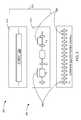
- the electronic system 100includes a memory sub-system 102 having a memory controller 104 and a memory array 106 .
- the electronic system 100includes a host system 108 communicating with the memory sub-system 102 .
- the memory controller 104provides data control and management of the memory array 106 .
- the memory controller 104interfaces with the host system 108 and controls the memory array 106 to transfer data between the host system 108 and the memory array 106 .
- the memory array 106includes an array of memory devices 110 including flash memory devices or non-volatile memory devices.
- the memory array 106can include pages of data or information.
- the host system 108can request the memory controller 104 for reading, writing, and deleting data from or to the logical address space of the storage device that includes the memory array 106 .
- the memory devices 110can include chip selects 112 , which are defined as control inputs, for enabling the memory devices 110 .
- Each of the chip selects 112can be used to control the operation of one of the memory devices 110 .
- the memory devices 110are in active state for operation including reading, writing, or recycling. This is also true for sub addresses LUNs (logical units) within a device controlled by one chip select.
- the memory controller 104can include a control unit 202 , a storage unit 204 , a memory interface unit 206 , and a host interface unit 208 .
- the control unit 202can include a control interface 210 .
- the control unit 202can execute software 212 stored in the storage unit 204 to provide the intelligence of the memory controller 104 .
- the control unit 202can be implemented in a number of different manners.
- the control unit 202can be a processor, an embedded processor, a microprocessor, a hardware control logic, a hardware finite state machine (FSM), a digital signal processor (DSP), or a combination thereof.
- FSMhardware finite state machine
- DSPdigital signal processor
- the memory controller 104can include a signal envelope follower 221 , which is defined as a circuit used to monitor and produce signals.
- the signal envelope follower 221monitors or follows the outline of an alternating current (AC) signal.
- the signal envelope follower 221can use a discrete circuit than the circuit used for the control unit 202 for monitoring and producing signals.
- the signal envelope follower 221can also be a component of the control unit 202 .
- the signal envelope follower 221can also include hardware or software running on hardware for monitoring or following the outline of an AC signal.
- the signal envelope follower 221can monitor continuous wave signals and produce signals including patterned pulses, and signals with direct current envelopes.
- the signal envelope follower 221can be configured to recognize unique signals that cannot be recognized by other components of the memory controller 104 .
- the host system 108 of FIG. 1can also include the signal envelope follower 221 for detecting out-of-band ( 00 B) signaling and for performing speed negotiation operations.
- the control interface 210can be used for communication between the control unit 202 and other functional units in the memory controller 104 .
- the control interface 210can also be used for communication that is external to the memory controller 104 .
- the control interface 210can receive information from the other functional units or from external sources, or can transmit information to the other functional units or to external destinations.
- the external sources and the external destinationsrefer to sources and destinations external to the memory controller 104 .
- the control interface 210can be implemented in different ways and can include different implementations depending on which functional units or external units are being interfaced with the control interface 210 .
- the control interface 210can be implemented with dedicated hardware such is an application-specific integrated circuit (ASIC), configurable hardware such as an FPGA (Field programmable Gate Array), discrete electronic hardware, or a combination thereof.
- ASICapplication-specific integrated circuit
- FPGAField programmable Gate Array
- the storage unit 204can include hardware, control firmware, and the software 212 .
- the storage unit 204can contain a volatile memory, a non-volatile memory, an internal memory, an external memory, or a combination thereof.
- the storage unit 204can be a non-volatile storage such as non-volatile random access memory (NVRAM), Flash memory, disk storage, or a volatile storage such as static random access memory (SRAM).
- NVRAMnon-volatile random access memory
- SRAMstatic random access memory
- the storage unit 204can include a storage interface 214 .
- the storage interface 214can also be used for communication that is external to the memory controller 104 .
- the storage interface 214can receive information from the other functional units or from external sources, or can transmit information to the other functional units or to external destinations.
- the external sources and the external destinationsrefer to sources and destinations external to the memory controller 104 .
- the storage interface 214can include different implementations depending on which functional units or external units are being interfaced with the storage unit 204 .
- the storage interface 214can be implemented with technologies and techniques similar to the implementation of the control interface 210 .
- the memory interface unit 206can enable external communication to and from the memory controller 104 .
- the memory interface unit 206can permit the memory controller 104 to communicate with the memory array 106 of FIG. 1 .
- the memory interface unit 206can include a memory interface 216 .
- the memory interface 216can be used for communication between the memory interface unit 206 and other functional units in the memory controller 104 .
- the memory interface 216can receive information from the other functional units or can transmit information to the other functional units.
- the memory interface 216can include different implementations depending on which functional units are being interfaced with the memory interface unit 206 .
- the memory interface 216can be implemented with technologies and techniques similar to the implementation of the control interface 210 .
- the host interface unit 208allows the host system 108 of FIG. 1 to interface and interact with the memory controller 104 .
- the host interface unit 208can include a host interface 218 to provide communication mechanism between the host interface unit 208 and the host system 108 .
- the control unit 202can operate the host interface unit 208 to send control or status information generated by the memory controller 104 to the host system 108 .
- the control unit 202can also execute the software 212 for the other functions of the memory controller 104 .
- the control unit 202can further execute the software 212 for interaction with the memory array 106 via the memory interface unit 206 .
- the functional units in the memory controller 104can work individually and independently of the other functional units.
- the memory controller 104is described by operation of the memory controller 104 with the host system 108 and the memory array 106 . It is understood that the memory controller 104 , the host system 108 , and the memory array 106 can operate any of the modules and functions of the memory controller 104 .
- FIG. 3therein is shown an example diagram of the system modification control mechanism of the electronic system 100 of FIG. 1 .
- the exampleincludes three sample signals sent from the host system 108 of FIG. 1 to the memory controller 104 of FIG. 1 .
- the signalscan include a continuous wave signal, which is defined as a non-modulated base frequency signal wave with a constant amplitude and frequency.
- a patterned signal 302is defined as a continuous wave signal, which includes a pattern of signaling bits for transmission.
- the patterns of the patterned signal 302can include active signal envelopes and null signals in specific sequences.
- the patterned signal 302can be an out-of-band signal 304 used for communication between components of the electronic system 100 .
- the patterned signal 302can include a pulse width time 306 and a pulse separation time 308 .
- the pulse width time 306is defined as a period of time that a pulse is active or during an active direct current envelope within the signal.
- the pulse width time 306can indicate that a pulse is on for a duration of 106.7 nanoseconds or 160 unit interval-out-of-band (UIOOB).
- the pulse separation time 308is defined as a period of time of a null signal or when the pulse is off within the patterned signal 302 .
- the pulse separation time 308can also have a duration of 106.7 nanoseconds and alternate with the pulse width time 306 to compose the pattern or sequence within the patterned signal 302 .
- the patterned signal 302can include a speed negotiation signal 310 .
- the speed negotiation signal 310is the out-of-band signal 304 used in the speed negotiation protocol of SATA devices.
- the speed negotiation signal 310can include COMREST, COMINT, and COMWAKE, which are used for handshaking between the host system 108 and the memory controller 104 .
- the speed negotiation signal 310can include the pulse width time 306 of 106.7 nanoseconds and the pulse separation time 308 of 106.7 nanoseconds as depicted by T1 in the diagram.
- the patterned signal 302can include a unique trigger 312 , which is defined as a signal for modifying settings on the memory sub-system 102 of FIG. 1 .
- the unique trigger 312can be used to trigger specific modes of operation or to trigger specific actions in the memory sub-system 102 .
- the unique trigger 312can trigger a firmware update for the memory sub-system 102 .
- the signal of the unique trigger 312can be different from the speed negotiation signal 310 by having different patterns, sequences, frequencies, durations, amplitudes, or a combination thereof.
- the pulse sequences that are associated with the unique trigger 312can be used to differentiate the patterned signal 302 from another, such as the SATA protocol signal used for COMWAKE.
- the durations of the pulse width time 306can be a ratio from a range of 2:1 to 10:1 to differentiate the unique trigger 312 from the speed negotiation signal 310 .
- the unique trigger 312can include a plurality of different signals that are each tied to a specific mode of operation or action to be performed by the memory sub-system 102 .
- the unique trigger 312can include a first trigger 313 and a second trigger 314 as two examples of the unique trigger 312 .
- the first trigger 313can include a sequence of the pulse width time 306 of T1 and T3 and alternating with the pulse separation time 308 of T2.
- the duration of T2can equal 320 nanoseconds/ 480 UIOOB and the duration of T3 can be three to six times the duration of the T1 time. Because the sequencing of the pulse width time 306 and the pulse separation time 308 of the first trigger 313 is out of characteristic of the speed negotiation signal 310 , the risk of false triggering is avoided.
- the first trigger 313can be the unique trigger 312 that is tied to executing a system recovery of the memory sub-system 102 .
- the second trigger 314can include a time break 316 , which is a signal with the pulse width time 306 with a long duration.
- the long duration of the pulse width time 306 of the time break 316is to distinguish the signal from the speed negotiation signal 310 for preventing false triggering.
- the second trigger 314can be the unique trigger 312 that is tied to executing a firmware update of the memory sub-system 102 . It is understood that the first trigger 313 and the second trigger 314 can be interchangeable in being tied to specific actions or modes of operation of the electronic system 100 .
- the electronic system 100eliminates the need for physically shorting two electrical points on the hardware boards of storage devices or the need for an overt hardware interaction by using the patterned signal 302 as the unique trigger 312 to modify settings on the electronic system 100 .
- the specific sequences and patterns within the unique trigger 312can trigger specific modes of operation of the memory sub-system 102 including updating or reverting firmware of the memory sub-system 102 .
- the unique trigger 312provides an alternative method to physical methods and removes the requirement to disassemble the device to have access to electrical points normally done during pin strapping. Thus, the risk to the electronic system 100 is reduced from the danger of physical damage caused by physical tampering.
- the electronic system 100can use specific sequences for the unique trigger 312 for special device operations outside normal drive operation such as triggering firmware updates using an out-of-band communications channel.
- the unique trigger 312can include the first trigger 313 and the second trigger 314 having different aspect ratios for the pulse width time 306 and the pulse separation time 308 to differentiate the unique trigger 312 from other SATA communication protocols for the prevention of false triggering.
- the time break 316provides the unique trigger 312 that is out of the specifications for the speed negotiation signal 310 , such as COMREST, COMWAKE, or COMINIT signaling, which avoids false triggering.
- the time break 316includes the pulse width time 306 that is at least three times the width of the pulse width time 306 for COMREST, COMWAKE, or COMINIT signaling, which prevents false triggering of other operations such as speed negotiation.
- the memory controller 104can include a power module 402 , a status module 406 , a signal module 412 , a recognizer module 418 , an operation module 420 , a change module 421 , and a power cycle module 437 .
- each moduleis indicated by a number and successively higher module numbers follow one another. Control flow can pass from one module to the next higher numbered module unless explicitly otherwise indicated.
- the control unit 202 of FIG. 2can be coupled to the power module 402 , the status module 406 , the signal module 412 , the recognizer module 418 , the operation module 420 , the change module 421 , and the power cycle module 437 for executing the modules.
- the power module 402detects a power up 404 of the electronic system 100 of FIG. 1 .
- the power module 402can be coupled to the status module 406 and the power cycle module 437 .
- the status module 406checks the condition or state of the memory sub-system 102 of FIG. 1 . For example, the status module 406 can determine that the memory sub-system 102 is in a functioning state and is capable of proceeding with data storage operations. The status module 406 can determine if a firmware 407 of the memory sub-system 102 is functioning properly. The status module 406 can also determine a non-functional state 408 of the memory sub-system 102 .
- the non-functional state 408is defined as a firmware failure, which can cause boot up issues with the memory sub-system 102 .
- the non-functional state 408can indicate that the memory sub-system 102 is corrupted or an incorrect version of the firmware 407 is installed.
- the non-functional state 408can be caused by a previous failed attempt at modifying the firmware 407 such as an installation interruption or a power failure during a firmware update.
- the status module 406can also generate a revert signal 410 .
- the revert signal 410is the unique trigger 312 of FIG. 3 for executing a firmware reset for the memory sub-system 102 .
- the memory sub-system 102can be reverted back to an original factory version of the firmware 407 or reverted back to an earlier valid version of the firmware 407 .
- the signal module 412can receive the patterned signal 302 of FIG. 3 .
- the signal module 412can receive the revert signal 410 .
- the patterned signal 302can be received from the status module 406 or from the host system 108 of FIG. 1 .
- the host system 108can also send the patterned signal 302 to the signal module 412 .
- the signal module 412can be coupled to the status module 406 , the recognizer module 418 , the signal envelope follower 221 of FIG. 2 , and the host system 108 .
- the signal module 412can include a window module 414 .
- the window module 414can determine an available period 416 for the signal module 412 to accept the patterned signal 302 .
- the window module 414can determine that the available period 416 is at all times while the memory sub-system 102 is operating.
- the signal envelope follower 221can be operating in the system background for receiving the patterned signal 302 .
- the window module 414can determine that the available period 416 is only for a short period after the power up 404 .
- the patterned signal 302will not be valid or accepted by the signal module 412 if the patterned signal 302 is sent to the signal module 412 after the available period 416 .
- the available period 416can be used to prevent unintended or unauthorized uses for increasing the security and the reliability of the electronic system 100 .
- the recognizer module 418interprets and recognizes the unique trigger 312 from the patterned signal 302 received by the signal module 412 .
- the recognizer module 418can differentiate the unique trigger 312 from other examples of the patterned signals 302 .
- the recognizer module 418can recognize the revert signal 410 as being different from the speed negotiation signal 310 of FIG. 3 .
- the recognizer module 418can recognize the patterns within the patterned signal 302 including tracking the pulse width time 306 of FIG. 3 and the pulse separation time 308 of FIG. 3 .
- the recognizer module 418can be coupled to the signal envelope follower 221 of for monitoring and recognizing the unique trigger 312 using the control unit 202 of FIG. 2 or a separate and discrete circuit.
- the recognizer module 418can use the signal envelope follower 221 for monitoring the first trigger 313 of FIG. 3 and the second trigger 314 of FIG. 3 .
- the recognizer module 418can also use a trigger envelope follower, which is a second and dedicated envelope follower than the signal envelope follower 221 , for monitoring the patterned signal 302 having the unique trigger 312 .
- the unique trigger 312can include a plurality of different signals that are each tied to a specific trigger for modifying operational settings on the memory sub-system 102 .
- the unique trigger 312can include a version signal 432 , an update signal 434 , a security signal 436 , and a manufacturing signal 438 .
- the version signal 432is the unique trigger 312 for changing the firmware 407 of the memory sub-system 102 to a specific version.
- the update signal 434is the unique trigger 312 for updating the firmware 407 to the newest available version.
- the security signal 436is the unique trigger 312 for enabling and disabling security features of the memory sub-system 102 .
- the manufacturing signal 438is the unique trigger 312 for enabling and disabling a diagnostic or special factory mode of operation for the memory sub-system 102 .
- the recognizer module 418can be coupled to the operation module 420 for selecting a mode of operation associated with each of the types of the unique trigger 312 .
- the version signal 432 , the update signal 434 , the security signal 436 , the manufacturing signal 438 , and the revert signal 410can have a sequence that is similar to the examples of the unique trigger 312 shown in FIG. 3 .
- the version signal 432can have the same sequence as the first trigger 313 and the update signal 434 can have the same sequence as the second trigger 314 .
- the recognizer module 418can also receive and recognize multiple triggers or multiple instances of the unique trigger 312 .
- the recognizer module 418can receive the first trigger 313 , and subsequently the second trigger 314 for modifying two different settings for the memory sub-system 102 in a single power cycle.
- the first trigger 313can enable security features in the memory sub-system 102 and the second trigger 314 can trigger a diagnostic mode of operation within the same power cycle.
- the recognizer module 418can also recognize if the patterned signal 302 includes multiple triggers within the same transmission.
- the patterned signal 302 received by the signal module 412can include both the patterns for the first trigger 313 and the second trigger 314 .
- Two different settings for the memory sub-system 102can be manipulated within a single power cycle using one transmission of the patterned signal 302 .
- the operation module 420selects an operational mode 423 for the memory sub-system 102 based on the unique trigger 312 received.
- the operational mode 423allows the modification of settings and specific operations of the memory sub-system 102 .
- the operational mode 423can include modes of operation outside of normal device operation of the electronic system 100 .
- the operation module 420can be coupled to the change module 421 for executing modifications.
- the operational mode 423can include enabling drive functions including updating the firmware 407 , executing special run modes, and modifying security settings.
- the operational mode 423can include a reset mode 422 , a version mode 424 , an update mode 426 , a security mode 428 , and a manufacturing mode 430 .
- the reset mode 422enables a reset of the memory sub-system 102 to an original factory condition including the original version of the firmware.
- the operational mode 423can receive the revert signal 410 from the recognizer module 418 for selecting the reset mode 422 .
- the non-functional state 408can be removed from the memory sub-system 102 by enabling a reset of the firmware 407 for returning to a functioning state.
- the version mode 424can enable the firmware 407 of the memory sub-system 102 to be changed to any previous version of the firmware 407 stored in the memory sub-system 102 .
- the version mode 424can enable the memory sub-system 102 to be flashed by any valid version of the firmware 407 that is stored in the storage unit 204 of FIG. 2 .
- the update mode 426can enable the firmware 407 of the memory sub-system 102 to be updated to a new version after receiving the unique trigger 312 .
- the new and updated version of the firmware 407can be stored in the storage unit 204 .
- the security mode 428can enable the toggling of secure erase features built into the memory sub-system 102 .
- the security mode 428can be enabled or disabled after receiving the unique trigger 312 associated with the mode.
- the security mode 428can be used for secure erase operations allowing the information in the memory sub-system 102 to be quickly erased or destroyed.
- the security mode 428can also be disabled to prevent accidental erasures.
- the manufacturing mode 430can enable the memory sub-system 102 to enter into a manufacturing test environment mode or a diagnostic mode after receiving the unique trigger 312 .
- the manufacturing mode 430can allow special commands and actions used during the manufacturing stage or repair periods for the memory sub-system 102 .
- the change module 421perform a system state change 425 on the memory sub-system 102 based on the operational mode 423 selected by the operation module 420 .
- the system state change 425is defined as a modification of a setting or modification of the operational mode 423 of the memory sub-system 102 .
- the system state change 425can be a change from one of the operational mode 423 to another of the operational mode 423 .
- the system state change 425can also include a change from the non-functional state 408 to another of the operational mode 423 .
- the change module 421can execute the processes of the reset mode 422 or the version mode 424 to execute a reversion 427 of the firmware 407 .
- the reversion 427is defined as a process for reverting the firmware 407 to an original factory version of the firmware 407 or to a previously stored version of the firmware 407 .
- the change module 421can be coupled to the storage unit 204 for accessing firmware information.
- the power cycle module 437performs a reboot of the memory sub-system 102 .
- the rebooting of the memory sub-system 102may be necessary after the system state change 425 , such as installing a new or different version of the firmware 407 .
- the power cycle module 437can be coupled to the power module 402 for detecting the power up 404 .
- the status module 406can check the status of the memory sub-system 102 after a reboot.
- the electronic system 100describes the module functions or order as an example.
- the modulescan be partitioned differently.
- the power module 402 , the status module 406 , the signal module 412 , the recognizer module 418 , the operation module 420 , the change module 421 , and the power cycle module 437can be implemented as one module or with lesser number of modules.
- Each of the modulescan operate individually and independently of the other modules.
- the electronic system 100eliminates the need for physically shorting two electrical points on the hardware boards of storage devices or the need for an overt hardware interaction by using the patterned signal 302 as the unique trigger 312 to modify settings on the electronic system 100 .
- the specific sequences and patterns within the unique trigger 312can trigger specific modes of operation of the memory sub-system 102 including updating or reverting firmware of the memory sub-system 102 .
- the unique trigger 312provides an alternative method to physical methods and removes the requirement to disassemble the device to have access to electrical points normally done during pin strapping. Thus, the risk to the electronic system 100 from the danger of physical damage caused by physical tampering is reduced
- the electronic system 100can use specific sequences for the unique trigger 312 for special device operations outside normal drive operation such as triggering an update of the firmware 407 using an out-of-band communications channel.
- the unique trigger 312can include the first trigger 313 and the second trigger 314 having different aspect ratios for the pulse width time 306 and the pulse separation time 308 to differentiate the unique trigger 312 from other SATA communication protocols for the prevention of false triggering.
- the patterned signal 302 having the unique trigger 312 associated with different version of the firmware 407allows for the reversion 427 of any version of the firmware 407 that is available.
- various versions of the firmware 407can be stored on the memory sub-system 102 and each version of the firmware 407 can be tied to a different trigger signal.
- the unique trigger 312 associated with different versions of the firmware 407allows for flexibility in installing and modifying the firmware 407 on the memory sub-system 102 .
- the available period 416provides security and reliability to the electronic system 100 by determine time periods for accepting the unique trigger 312 .
- the available period 416can be for all times during operation of the memory sub-system 102 or for a short period after the power up 404 .
- the discovery of the available period 416can be used to prevent unintended or unauthorized modifications to the electronic system 100 .
- the electronic system 100increases the speed and efficiency of the burn-in and bring-up processes during the manufacturing stage of a large number of devices because the unique trigger 312 can be sent to multiple devices simultaneously. Further for example, the unique trigger 312 sent to the memory controller 104 eliminates the need to attach special cables to each device during a volume manufacturing process and thus also provides additional efficiency to the manufacturing and testing stages of the electronic system 100 .
- the time break 316 of FIG. 3provides the unique trigger 312 that is out of the specifications for the speed negotiation signal 310 , such as COMREST, COMWAKE, or COMINIT signaling, which avoids false triggering.
- the time break 316includes the pulse width time 306 that is at least three times the width of the pulse width time 306 for COMREST, COMWAKE, or COMINIT signaling, which prevents fails triggering of other operations such as speed negotiation.
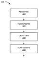
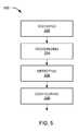
- the method 500includes: receiving a patterned signal in a block 502 ; recognizing an unique trigger from the patterned signal in a block 504 ; detecting an operational mode from the unique trigger in a block 506 ; and configuring a system state change of a memory-sub-system based on the operational mode in a block 508 .
- the electronic system 100 of the present inventionfurnishes important and heretofore unknown and unavailable solutions, capabilities, and functional aspects for an electronic system with read disturb management mechanism.
- the resulting method, process, apparatus, device, product, and/or systemis straightforward, cost-effective, uncomplicated, highly versatile, accurate, sensitive, and effective, and can be implemented by adapting known components for ready, efficient, and economical manufacturing, application, and utilization.
- Another important aspect of the present inventionis that it valuably supports and services the historical trend of reducing costs, simplifying systems, and increasing performance. These and other valuable aspects of the present invention consequently further the state of the technology to at least the next level.
Landscapes
- Engineering & Computer Science (AREA)
- Theoretical Computer Science (AREA)
- Software Systems (AREA)
- General Engineering & Computer Science (AREA)
- Physics & Mathematics (AREA)
- General Physics & Mathematics (AREA)
- Computer Security & Cryptography (AREA)
- Storage Device Security (AREA)
- Stored Programmes (AREA)
Abstract
Description
Claims (18)
Priority Applications (3)
| Application Number | Priority Date | Filing Date | Title |
|---|---|---|---|
| US13/851,928US9043780B2 (en) | 2013-03-27 | 2013-03-27 | Electronic system with system modification control mechanism and method of operation thereof |
| PCT/US2014/031465WO2014160612A1 (en) | 2013-03-27 | 2014-03-21 | Electronic system with system modification control mechanism and method of operation thereof |
| TW103111515ATW201447762A (en) | 2013-03-27 | 2014-03-27 | Electronic system with system modification control mechanism and method of operation thereof |
Applications Claiming Priority (1)
| Application Number | Priority Date | Filing Date | Title |
|---|---|---|---|
| US13/851,928US9043780B2 (en) | 2013-03-27 | 2013-03-27 | Electronic system with system modification control mechanism and method of operation thereof |
Publications (2)
| Publication Number | Publication Date |
|---|---|
| US20140298004A1 US20140298004A1 (en) | 2014-10-02 |
| US9043780B2true US9043780B2 (en) | 2015-05-26 |
Family
ID=50729798
Family Applications (1)
| Application Number | Title | Priority Date | Filing Date |
|---|---|---|---|
| US13/851,928Active2033-06-03US9043780B2 (en) | 2013-03-27 | 2013-03-27 | Electronic system with system modification control mechanism and method of operation thereof |
Country Status (3)
| Country | Link |
|---|---|
| US (1) | US9043780B2 (en) |
| TW (1) | TW201447762A (en) |
| WO (1) | WO2014160612A1 (en) |
Families Citing this family (3)
| Publication number | Priority date | Publication date | Assignee | Title |
|---|---|---|---|---|
| EP2747131B1 (en)* | 2012-12-18 | 2015-07-01 | Nxp B.V. | Method of processing a silicon wafer |
| US20180304086A1 (en)* | 2017-04-19 | 2018-10-25 | Qualcomm Incorporated | Wireless communication frame design for medical implants |
| CN111858438B (en)* | 2019-04-30 | 2022-03-01 | 瑞昱半导体股份有限公司 | Interface connection device and method |
Citations (201)
| Publication number | Priority date | Publication date | Assignee | Title |
|---|---|---|---|---|
| US4048481A (en) | 1974-12-17 | 1977-09-13 | Honeywell Information Systems Inc. | Diagnostic testing apparatus and method |
| US4839587A (en) | 1988-03-29 | 1989-06-13 | Digital Equipment Corporation | Test fixture for tab circuits and devices |
| US5034744A (en) | 1988-11-09 | 1991-07-23 | Nakamichi Corporation | Deglitching circuit |
| US5210854A (en)* | 1989-06-14 | 1993-05-11 | Digital Equipment Corporation | System for updating program stored in eeprom by storing new version into new location and updating second transfer vector to contain starting address of new version |
| US5311395A (en) | 1992-10-29 | 1994-05-10 | Ncr Corporation | Surface mount heat sink |
| US5479638A (en) | 1993-03-26 | 1995-12-26 | Cirrus Logic, Inc. | Flash memory mass storage architecture incorporation wear leveling technique |
| US5930504A (en) | 1996-07-22 | 1999-07-27 | Intel Corporation | Dynamic nonvolatile memory update in a computer system |
| US5949785A (en) | 1995-11-01 | 1999-09-07 | Whittaker Corporation | Network access communications system and methodology |
| US5963983A (en) | 1996-04-15 | 1999-10-05 | International Business Machines Corporation | Method and apparatus for dynamically creating conversion tables to access a semiconductor memory device |
| US6069827A (en) | 1995-09-27 | 2000-05-30 | Memory Corporation Plc | Memory system |
| US6091652A (en) | 1998-12-11 | 2000-07-18 | Lsi Logic Corporation | Testing semiconductor devices for data retention |
| US6275436B1 (en) | 1993-04-08 | 2001-08-14 | Hitachi, Ltd | Flash memory control method and apparatus processing system therewith |
| US6345367B1 (en) | 1996-07-11 | 2002-02-05 | Memory Corporation Plc | Defective memory block handling system by addressing a group of memory blocks for erasure and changing the content therewith |
| US6356447B2 (en) | 2000-06-20 | 2002-03-12 | Adc Telecommunications, Inc. | Surface mounted conduction heat sink |
| US6381670B1 (en) | 1997-01-07 | 2002-04-30 | Aplus Flash Technology, Inc. | Flash memory array having maximum and minimum threshold voltage detection for eliminating over-erasure problem and enhancing write operation |
| US20020056025A1 (en) | 2000-11-07 | 2002-05-09 | Qiu Chaoxin C. | Systems and methods for management of memory |
| US6412080B1 (en) | 1999-02-23 | 2002-06-25 | Microsoft Corporation | Lightweight persistent storage system for flash memory devices |
| US20020159285A1 (en) | 2000-03-01 | 2002-10-31 | Stephen Morley | Data balancing scheme in solid state storage devices |
| US20030033308A1 (en) | 2001-08-03 | 2003-02-13 | Patel Sujal M. | System and methods for providing a distributed file system utilizing metadata to track information about data stored throughout the system |
| US6529997B1 (en) | 2000-08-11 | 2003-03-04 | Storage Technology Corporation | Apparatus and method for writing and reading data to and from a virtual volume of redundant storage devices |
| US20030046603A1 (en) | 1989-04-13 | 2003-03-06 | Eliyahou Harari | Flash EEprom system |
| US20030074592A1 (en) | 2001-10-15 | 2003-04-17 | Fujitsu Limited | Information processing apparatus, power supply control method for plural information processing apparatuses, and storage medium therefore |
| US6552581B1 (en) | 2000-08-25 | 2003-04-22 | Agere Systems Inc. | Current recycling circuit and a method of current recycling |
| US6587915B1 (en) | 1999-09-29 | 2003-07-01 | Samsung Electronics Co., Ltd. | Flash memory having data blocks, spare blocks, a map block and a header block and a method for controlling the same |
| US20030163633A1 (en) | 2002-02-27 | 2003-08-28 | Aasheim Jered Donald | System and method for achieving uniform wear levels in a flash memory device |
| US6618249B2 (en) | 2002-02-05 | 2003-09-09 | Quantum Corporation | Thermal cooling system for densely packed storage devices |
| US6661503B1 (en) | 1997-11-21 | 2003-12-09 | Hitachi, Ltd. | Method for manufacturing optic transmission modules and system for inspecting bit error rate characters |
| US6728913B1 (en) | 2000-02-25 | 2004-04-27 | Advanced Micro Devices, Inc. | Data recycling in memory |
| US20040080985A1 (en) | 2002-10-28 | 2004-04-29 | Sandisk Corporation, A Delaware Corporation | Maintaining erase counts in non-volatile storage systems |
| US6763424B2 (en) | 2001-01-19 | 2004-07-13 | Sandisk Corporation | Partial block data programming and reading operations in a non-volatile memory |
| US6775792B2 (en) | 2001-01-29 | 2004-08-10 | Snap Appliance, Inc. | Discrete mapping of parity blocks |
| US20040252670A1 (en) | 2003-06-12 | 2004-12-16 | Nokia Corporation | Adaptive power margin adjustment for a 1xEV-DV system |
| US20050021904A1 (en) | 2003-06-05 | 2005-01-27 | Stmicroelectronics S.R.L. | Mass memory device based on a flash memory with multiple buffers |
| US6850443B2 (en) | 1991-09-13 | 2005-02-01 | Sandisk Corporation | Wear leveling techniques for flash EEPROM systems |
| US6854070B2 (en) | 2000-01-25 | 2005-02-08 | Hewlett-Packard Development Company, L.P. | Hot-upgrade/hot-add memory |
| US20050038792A1 (en) | 2003-08-14 | 2005-02-17 | Johnson Ted C. | Apparatus and method for operating circular files |
| US6871304B2 (en) | 2002-08-12 | 2005-03-22 | Nortel Networks Limited | Method and apparatus for adjusting receiver voltage threshold and phase sampling point using FEC counts |
| US20050076102A1 (en)* | 2003-09-18 | 2005-04-07 | Alan Chen | Intelligent modular server management system for selectively operating and locating a plurality of computers |
| US20050073884A1 (en) | 2003-10-03 | 2005-04-07 | Gonzalez Carlos J. | Flash memory data correction and scrub techniques |
| US6903972B2 (en) | 2003-07-30 | 2005-06-07 | M-Systems Flash Disk Pioneers Ltd. | Different methods applied for archiving data according to their desired lifetime |
| US6906961B2 (en) | 2003-06-24 | 2005-06-14 | Micron Technology, Inc. | Erase block data splitting |
| US20060015683A1 (en) | 2004-06-21 | 2006-01-19 | Dot Hill Systems Corporation | Raid controller using capacitor energy source to flush volatile cache data to non-volatile memory during main power outage |
| US20060020745A1 (en) | 2004-07-21 | 2006-01-26 | Conley Kevin M | Fat analysis for optimized sequential cluster management |
| US20060136682A1 (en) | 2004-12-21 | 2006-06-22 | Sriram Haridas | Method and apparatus for arbitrarily initializing a portion of memory |
| US20060143475A1 (en)* | 2004-12-29 | 2006-06-29 | Herbert Howard C | Updating firmware securely over a network |
| US20060143365A1 (en) | 2002-06-19 | 2006-06-29 | Tokyo Electron Device Limited | Memory device, memory managing method and program |
| US7082495B2 (en) | 2002-06-27 | 2006-07-25 | Microsoft Corporation | Method and apparatus to reduce power consumption and improve read/write performance of hard disk drives using non-volatile memory |
| US7107389B2 (en) | 2002-08-29 | 2006-09-12 | Matsushita Electric Industrial Co., Ltd. | Semiconductor memory device and method for writing data into flash memory |
| US20060253641A1 (en) | 2003-08-07 | 2006-11-09 | Micron Technology, Inc. | Multiple erase block tagging in a flash memory device |
| US7139864B2 (en) | 2003-12-30 | 2006-11-21 | Sandisk Corporation | Non-volatile memory and method with block management system |
| US20060282644A1 (en) | 2005-06-08 | 2006-12-14 | Micron Technology, Inc. | Robust index storage for non-volatile memory |
| US20060294574A1 (en) | 2005-06-22 | 2006-12-28 | Cha Sang H | Apparatuses and methods for receiving software/firmware |
| US20070050536A1 (en) | 2005-09-01 | 2007-03-01 | Cypress Semiconductor Corporation | Flash drive fast wear leveling |
| US20070061511A1 (en) | 2005-09-15 | 2007-03-15 | Faber Robert W | Distributed and packed metadata structure for disk cache |
| US20070083779A1 (en) | 2005-10-07 | 2007-04-12 | Renesas Technology Corp. | Semiconductor integrated circuit device and power consumption control device |
| US7233497B2 (en) | 2004-10-06 | 2007-06-19 | Hewlett-Packard Development Company, L.P. | Surface mount heat sink |
| US7243186B2 (en) | 2003-12-22 | 2007-07-10 | Phison Electronics Corp. | Method of optimizing performance of flash memory |
| US20070234004A1 (en) | 2006-03-31 | 2007-10-04 | Takashi Oshima | Memory system and controller |
| US20070260811A1 (en) | 2006-05-08 | 2007-11-08 | Merry David E Jr | Systems and methods for measuring the useful life of solid-state storage devices |
| US20070263444A1 (en) | 2006-05-15 | 2007-11-15 | Gorobets Sergey A | Non-Volatile Memory System with End of Life Calculation |
| US7298888B2 (en) | 2002-10-23 | 2007-11-20 | Hamar Laser Instruments, Inc. | Electronic level sensor |
| US20070276973A1 (en) | 2004-09-30 | 2007-11-29 | Intel Corporation | Managing queues |
| US7330927B1 (en) | 2003-05-07 | 2008-02-12 | Avago Technologies General Ip (Singapore) Pte. Ltd. | Apparatus and methodology for a pointer manager |
| US7333364B2 (en) | 2000-01-06 | 2008-02-19 | Super Talent Electronics, Inc. | Cell-downgrading and reference-voltage adjustment for a multi-bit-cell flash memory |
| US20080046630A1 (en) | 2006-08-21 | 2008-02-21 | Sandisk Il Ltd. | NAND flash memory controller exporting a logical sector-based interface |
| US20080052446A1 (en) | 2006-08-28 | 2008-02-28 | Sandisk Il Ltd. | Logical super block mapping for NAND flash memory |
| US7350101B1 (en) | 2002-12-23 | 2008-03-25 | Storage Technology Corporation | Simultaneous writing and reconstruction of a redundant array of independent limited performance storage devices |
| US20080082736A1 (en) | 2004-03-11 | 2008-04-03 | Chow David Q | Managing bad blocks in various flash memory cells for electronic data flash card |
| US7355896B2 (en) | 2005-12-22 | 2008-04-08 | Chartered Semiconductor Manufacturing Ltd. | System for improving endurance and data retention in memory devices |
| US20080183918A1 (en) | 2007-01-31 | 2008-07-31 | Microsoft Corporation | Extending flash drive lifespan |
| EP1956489A2 (en) | 2007-02-07 | 2008-08-13 | Hitachi, Ltd. | Storage control unit and data management method |
| US7434122B2 (en) | 2004-08-04 | 2008-10-07 | Samsung Electronics Co., Ltd. | Flash memory device for performing bad block management and method of performing bad block management of flash memory device |
| US7441067B2 (en) | 2004-11-15 | 2008-10-21 | Sandisk Corporation | Cyclic flash memory wear leveling |
| EP1990921A2 (en) | 2007-05-07 | 2008-11-12 | Broadcom Corporation | Operational parameter adaptable LDPC (low density parity check) decoder |
| US20080313505A1 (en) | 2007-06-14 | 2008-12-18 | Samsung Electronics Co., Ltd. | Flash memory wear-leveling |
| US20090019321A1 (en) | 2007-07-09 | 2009-01-15 | Micron Technolgy. Inc. | Error correction for memory |
| US20090083587A1 (en) | 2007-09-26 | 2009-03-26 | Jien-Hau Ng | Apparatus and method for selectively enabling and disabling a squelch circuit across AHCI and SATA power states |
| US20090089485A1 (en) | 2007-09-27 | 2009-04-02 | Phison Electronics Corp. | Wear leveling method and controller using the same |
| WO2009042298A1 (en) | 2007-09-26 | 2009-04-02 | Rambus Inc. | Flash memory refresh |
| US7516267B2 (en) | 2005-11-03 | 2009-04-07 | Intel Corporation | Recovering from a non-volatile memory failure |
| US20090125670A1 (en) | 2001-08-24 | 2009-05-14 | Micron Technology, Inc. | Erase block management |
| US20090138654A1 (en) | 2006-12-11 | 2009-05-28 | Pantas Sutardja | Fatigue management system and method for hybrid nonvolatile solid state memory system |
| US20090146721A1 (en) | 2007-12-07 | 2009-06-11 | Renesas Technology Corp. | Oob (out of band) detection circuit and serial ata system |
| US20090157948A1 (en) | 2007-12-14 | 2009-06-18 | Spansion Llc | Intelligent memory data management |
| US20090164702A1 (en) | 2007-12-21 | 2009-06-25 | Spansion Llc | Frequency distributed flash memory allocation based on free page tables |
| US20090172262A1 (en) | 2007-12-27 | 2009-07-02 | Pliant Technology, Inc. | Metadata rebuild in a flash memory controller following a loss of power |
| US20090228761A1 (en) | 2008-03-07 | 2009-09-10 | Anobit Technologies Ltd | Efficient readout from analog memory cells using data compression |
| US20090259896A1 (en) | 2008-04-10 | 2009-10-15 | Phison Electronics Corp. | Bad block identifying method for flash memory, storage system, and controller thereof |
| US20090259819A1 (en) | 2008-04-09 | 2009-10-15 | Skymedi Corporation | Method of wear leveling for non-volatile memory |
| US7613871B2 (en) | 2005-06-21 | 2009-11-03 | Hitachi, Ltd. | Storage system using a flash memory partitioned with write-once and rewritable blocks |
| US7620769B2 (en) | 2000-01-06 | 2009-11-17 | Super Talent Electronics, Inc. | Recycling partially-stale flash blocks using a sliding window for multi-level-cell (MLC) flash memory |
| US20090287975A1 (en) | 2008-05-15 | 2009-11-19 | Samsung Electronics Co., Ltd. | Memory device and method of managing memory data error |
| US7639532B2 (en) | 2007-10-10 | 2009-12-29 | Micron Technology, Inc. | Non-equal threshold voltage ranges in MLC NAND |
| US20090327581A1 (en) | 2008-06-30 | 2009-12-31 | Coulson Richard L | Nand memory |
| US20090327591A1 (en) | 2008-06-25 | 2009-12-31 | Stec, Inc. | Slc-mlc combination flash storage device |
| US20090323419A1 (en) | 2008-06-26 | 2009-12-31 | Sdc Micro Inc. | Read-time wear-leveling method in storage system using flash memory device |
| US20100017650A1 (en) | 2008-07-19 | 2010-01-21 | Nanostar Corporation, U.S.A | Non-volatile memory data storage system with reliability management |
| US20100023674A1 (en) | 2008-07-28 | 2010-01-28 | Aviles Joaquin J | Flash DIMM in a Standalone Cache Appliance System and Methodology |
| US7661054B2 (en) | 2005-09-30 | 2010-02-09 | Intel Corporation | Methods and arrangements to remap degraded storage blocks |
| US20100050053A1 (en) | 2008-08-22 | 2010-02-25 | Wilson Bruce A | Error control in a flash memory device |
| US7679948B2 (en) | 2008-06-05 | 2010-03-16 | Sun Microsystems, Inc. | Write and read assist circuit for SRAM with power recycling |
| US7693422B2 (en) | 2004-09-28 | 2010-04-06 | Alcatel-Lucent Usa Inc. | Constraint-based design of optical transmission systems |
| US20100128537A1 (en) | 2008-11-25 | 2010-05-27 | Mohammed Suhail | Method of programming a non-volatile memory |
| US20100138592A1 (en) | 2008-12-02 | 2010-06-03 | Samsung Electronics Co. Ltd. | Memory device, memory system and mapping information recovering method |
| US7738502B2 (en) | 2006-09-01 | 2010-06-15 | Intel Corporation | Signal noise filtering in a serial interface |
| US7743216B2 (en) | 2006-06-30 | 2010-06-22 | Seagate Technology Llc | Predicting accesses to non-requested data |
| US20100169541A1 (en) | 2008-12-30 | 2010-07-01 | Guy Freikorn | Method and apparatus for retroactive adaptation of data location |
| US20100174845A1 (en) | 2009-01-05 | 2010-07-08 | Sergey Anatolievich Gorobets | Wear Leveling for Non-Volatile Memories: Maintenance of Experience Count and Passive Techniques |
| US20100217898A1 (en) | 2009-02-24 | 2010-08-26 | Seagate Technology Llc | Receiver training during a sata out of band sequence |
| US20100217915A1 (en) | 2009-02-23 | 2010-08-26 | International Business Machines Corporation | High availability memory system |
| US20100228928A1 (en) | 2009-03-04 | 2010-09-09 | Micron Technology, Inc. | Memory block selection |
| US20100262795A1 (en) | 2009-04-08 | 2010-10-14 | Steven Robert Hetzler | System, method, and computer program product for analyzing monitor data information from a plurality of memory devices having finite endurance and/or retention |
| US20100262875A1 (en) | 2009-04-08 | 2010-10-14 | Steven Robert Hetzler | System, method, and computer program product for determining a retention behavior for at least one block of a memory device having finite endurance and/or retention |
| US20100262792A1 (en) | 2009-04-08 | 2010-10-14 | Steven Robert Hetzler | System, method, and computer program product for estimating when a reliable life of a memory device having finite endurance and/or retention, or portion thereof, will be expended |
| US7818525B1 (en) | 2009-08-12 | 2010-10-19 | Texas Memory Systems, Inc. | Efficient reduction of read disturb errors in NAND FLASH memory |
| US7827348B2 (en) | 2000-01-06 | 2010-11-02 | Super Talent Electronics, Inc. | High performance flash memory devices (FMD) |
| US7830164B2 (en) | 2008-04-22 | 2010-11-09 | Honeywell International Inc. | Ducted test socket |
| US20100287328A1 (en) | 2009-05-07 | 2010-11-11 | Seagate Technology Llc | Wear leveling technique for storage devices |
| US20100293367A1 (en) | 2009-05-13 | 2010-11-18 | Dell Products L.P. | System and Method for Optimizing Performance of an Information Handling System Component |
| US20100312954A1 (en) | 2007-04-27 | 2010-12-09 | Byung-Gil Jeon | Multi-Chip Semiconductor Devices Having Non-Volatile Memory Devices Therein |
| US20100318719A1 (en) | 2009-06-12 | 2010-12-16 | Micron Technology, Inc. | Methods, memory controllers and devices for wear leveling a memory |
| US20100332726A1 (en) | 2009-06-26 | 2010-12-30 | Solid State System Co., Ltd. | Structure and method for managing writing operation on mlc flash memory |
| US20110066788A1 (en) | 2009-09-15 | 2011-03-17 | International Business Machines Corporation | Container marker scheme for reducing write amplification in solid state devices |
| US20110072423A1 (en)* | 2009-09-18 | 2011-03-24 | Yamaha Corporation | Firmware update apparatus and program |
| US20110078393A1 (en) | 2009-09-29 | 2011-03-31 | Silicon Motion, Inc. | Memory device and data access method |
| US20110099342A1 (en) | 2009-10-22 | 2011-04-28 | Kadir Ozdemir | Efficient Logging for Asynchronously Replicating Volume Groups |
| US20110131365A1 (en) | 2009-11-30 | 2011-06-02 | Via Technologies, Inc. | Data Storage System and Method |
| US20110131447A1 (en) | 2009-11-30 | 2011-06-02 | Gyan Prakash | Automated modular and secure boot firmware update |
| US20110132000A1 (en) | 2009-12-09 | 2011-06-09 | Deane Philip A | Thermoelectric Heating/Cooling Structures Including a Plurality of Spaced Apart Thermoelectric Components |
| US20110145473A1 (en) | 2009-12-11 | 2011-06-16 | Nimble Storage, Inc. | Flash Memory Cache for Data Storage Device |
| US20110161775A1 (en) | 2009-12-24 | 2011-06-30 | Hanan Weingarten | System and method for setting a flash memory cell read threshold |
| US7979614B1 (en) | 2005-05-05 | 2011-07-12 | Marvell International Ltd. | Flash memory/disk drive interface and method for same |
| US20110191522A1 (en) | 2010-02-02 | 2011-08-04 | Condict Michael N | Managing Metadata and Page Replacement in a Persistent Cache in Flash Memory |
| US20110190963A1 (en) | 2010-01-29 | 2011-08-04 | Eurocopter Deutschland Gmbh | Method and system for an optimized utilization of energy resources of an electrical system |
| US20110191649A1 (en) | 2010-02-01 | 2011-08-04 | Samsung Electronics Co., Ltd. | Solid state drive and method of controlling an error thereof |
| US8001135B2 (en) | 2007-03-02 | 2011-08-16 | Kabushiki Kaisha Toshiba | Search support apparatus, computer program product, and search support system |
| US20110209032A1 (en) | 2010-02-24 | 2011-08-25 | Choi Jinhyeok | Nonvolatile Memory Devices with Age-Based Variability of Read Operations and Methods of Operating Same |
| US8010738B1 (en) | 2008-06-27 | 2011-08-30 | Emc Corporation | Techniques for obtaining a specified lifetime for a data storage device |
| US8028123B2 (en) | 2008-04-15 | 2011-09-27 | SMART Modular Technologies (AZ) , Inc. | Circular wear leveling |
| US20110239088A1 (en) | 2010-03-23 | 2011-09-29 | Apple Inc. | Non-regular parity distribution detection via metadata tag |
| US20110238892A1 (en) | 2010-03-24 | 2011-09-29 | Lite-On It Corp. | Wear leveling method of non-volatile memory |
| US8072805B2 (en) | 2009-08-18 | 2011-12-06 | Skymedi Corporation | Method and system of finding a read voltage for a flash memory |
| WO2011156466A2 (en) | 2010-06-08 | 2011-12-15 | Hewlett-Packard Development Company, L.P. | Storage caching |
| US20110314219A1 (en) | 2001-01-29 | 2011-12-22 | Overland Storage, Inc. | Systems andmethod for storing parity groups |
| US20110320687A1 (en) | 2010-06-29 | 2011-12-29 | International Business Machines Corporation | Reducing write amplification in a cache with flash memory used as a write cache |
| US8095724B2 (en) | 2008-02-05 | 2012-01-10 | Skymedi Corporation | Method of wear leveling for non-volatile memory and apparatus using via shifting windows |
| US8095765B2 (en) | 2009-03-04 | 2012-01-10 | Micron Technology, Inc. | Memory block management |
| US20120011336A1 (en) | 2010-04-22 | 2012-01-12 | Hitachi, Ltd. | Method of controlling information processing system and information apparatus |
| US20120008401A1 (en) | 2010-07-06 | 2012-01-12 | Michael Katz | Systems and methods for storing, retrieving, and adjusting read thresholds in flash memory storage system |
| US8117396B1 (en) | 2006-10-10 | 2012-02-14 | Network Appliance, Inc. | Multi-level buffer cache management through soft-division of a uniform buffer cache |
| US20120047409A1 (en) | 2010-08-23 | 2012-02-23 | Apple Inc. | Systems and methods for generating dynamic super blocks |
| US20120047320A1 (en) | 2010-08-20 | 2012-02-23 | Samsung Electronics Co., Ltd | Method and apparatus to interface semiconductor storage device and host to provide performance throttling of semiconductor storage device |
| US8127202B2 (en) | 2006-05-15 | 2012-02-28 | Apple Inc. | Use of alternative value in cell detection |
| US20120066450A1 (en) | 2009-02-11 | 2012-03-15 | Infinidat Ltd. | Virtualized storage system and method of operating thereof |
| US8145984B2 (en) | 2006-10-30 | 2012-03-27 | Anobit Technologies Ltd. | Reading memory cells using multiple thresholds |
| US8154921B2 (en) | 2008-05-09 | 2012-04-10 | Sandisk Technologies Inc. | Dynamic and adaptive optimization of read compare levels based on memory cell threshold voltage distribution |
| US8169825B1 (en) | 2008-09-02 | 2012-05-01 | Anobit Technologies Ltd. | Reliable data storage in analog memory cells subjected to long retention periods |
| US20120124046A1 (en) | 2010-11-16 | 2012-05-17 | Actifio, Inc. | System and method for managing deduplicated copies of data using temporal relationships among copies |
| US20120124273A1 (en) | 2010-11-12 | 2012-05-17 | Seagate Technology Llc | Estimating Wear of Non-Volatile, Solid State Memory |
| US20120151260A1 (en) | 2010-12-08 | 2012-06-14 | Arnaldo Zimmermann | System and Method for Autonomous NAND Refresh |
| US8209677B2 (en)* | 2007-05-21 | 2012-06-26 | Sony Corporation | Broadcast download system via broadband power line communication |
| JP2012129859A (en) | 2010-12-16 | 2012-07-05 | Nec Corp | Radio access network system, remote monitoring device, antenna angle control method, and antenna angle control program |
| US8219724B1 (en) | 2010-09-29 | 2012-07-10 | Emc Corporation | Flexibly managing I/O operations based on application awareness |
| US8219776B2 (en) | 2009-09-23 | 2012-07-10 | Lsi Corporation | Logical-to-physical address translation for solid state disks |
| US8228701B2 (en) | 2009-03-01 | 2012-07-24 | Apple Inc. | Selective activation of programming schemes in analog memory cell arrays |
| US8250621B2 (en)* | 2005-09-14 | 2012-08-21 | Lg Electronics Inc. | Broadcasting receiver and method for upgrading firmware |
| US20120213004A1 (en) | 2011-02-17 | 2012-08-23 | Samsung Electronics Co., Ltd. | Non-volatile memory device and related read method |
| US20120216085A1 (en) | 2011-02-23 | 2012-08-23 | Densbits Technologies Ltd. | Devices and method for wear estimation based memory management |
| US8254172B1 (en) | 2009-09-30 | 2012-08-28 | Western Digital Technologies, Inc. | Wear leveling non-volatile semiconductor memory based on erase times and program times |
| US8259506B1 (en) | 2009-03-25 | 2012-09-04 | Apple Inc. | Database of memory read thresholds |
| US20120239858A1 (en) | 2010-07-07 | 2012-09-20 | Stec, Inc. | Apparatus and method for determining an operating condition of a memory cell based on cycle information |
| US20120236656A1 (en) | 2010-07-09 | 2012-09-20 | Stec, Inc. | Apparatus and method for determining a read level of a memory cell based on cycle information |
| US8289801B2 (en) | 2009-09-09 | 2012-10-16 | Fusion-Io, Inc. | Apparatus, system, and method for power reduction management in a storage device |
| US20120266048A1 (en) | 2011-04-15 | 2012-10-18 | Chun Sing Jackson Chung | Dynamic Optimization of Back-End Memory System Interface |
| US8296534B1 (en) | 2007-06-29 | 2012-10-23 | Emc Corporation | Techniques for using flash-based memory in recovery processing |
| US8332578B2 (en) | 2009-07-31 | 2012-12-11 | Intel Corporation | Method and system to improve the performance of a multi-level cell (MLC) NAND flash memory |
| US20120324191A1 (en) | 2011-06-14 | 2012-12-20 | Western Digital Technologies, Inc. | System and method for performing data retention that incorporates environmental conditions |
| US20120331207A1 (en) | 2011-06-24 | 2012-12-27 | Lassa Paul A | Controller, Storage Device, and Method for Power Throttling Memory Operations |
| US20130007543A1 (en) | 2011-06-30 | 2013-01-03 | Seagate Technology Llc | Estimating temporal degradation of non-volatile solid-state memory |
| US20130007380A1 (en) | 2011-06-30 | 2013-01-03 | Seagate Technology Llc | Limiting activity rates that impact life of a data storage media |
| US8363413B2 (en) | 2010-09-13 | 2013-01-29 | Raytheon Company | Assembly to provide thermal cooling |
| US8369141B2 (en) | 2007-03-12 | 2013-02-05 | Apple Inc. | Adaptive estimation of memory cell read thresholds |
| US8386860B2 (en) | 2010-04-14 | 2013-02-26 | Phison Electronics Corp. | Methods of calculating compensation voltage and adjusting threshold voltage and memory apparatus and controller |
| US20130054881A1 (en) | 2011-08-31 | 2013-02-28 | SMART Storage Systems, Inc. | Electronic system with storage management mechanism and method of operation thereof |
| US20130060994A1 (en) | 2011-09-02 | 2013-03-07 | SMART Storage Systems, Inc. | Non-volatile memory management system with time measure mechanism and method of operation thereof |
| US20130073788A1 (en) | 2011-09-16 | 2013-03-21 | Apple Inc. | Weave sequence counter for non-volatile memory systems |
| US8407409B2 (en) | 2009-04-02 | 2013-03-26 | Hitachi, Ltd. | Metrics and management for flash memory storage life |
| US20130080691A1 (en) | 2007-12-05 | 2013-03-28 | Hanan Weingarten | Flash memory device with physical cell value deterioration accommodation and methods useful in conjunction therewith |
| US20130094289A1 (en) | 2011-10-18 | 2013-04-18 | Seagate Technology Llc | Determination of memory read reference and programming voltages |
| US20130100600A1 (en) | 2011-10-19 | 2013-04-25 | Hon Hai Precision Industry Co., Ltd. | Computer system with airflow guiding duct |
| US20130124792A1 (en) | 2011-02-03 | 2013-05-16 | Stec, Inc. | Erase-suspend system and method |
| US8464106B2 (en) | 2009-08-24 | 2013-06-11 | Ocz Technology Group, Inc. | Computer system with backup function and method therefor |
| US20130151753A1 (en) | 2011-12-09 | 2013-06-13 | Sandisk Technologies Inc. | Systems and methods of updating read voltages in a memory |
| US8503238B1 (en) | 2010-07-21 | 2013-08-06 | Sk Hynix Memory Solutions Inc. | Error recovery for flash memory |
| US20130238833A1 (en) | 2012-03-08 | 2013-09-12 | Apple Inc. | Heuristics for programming data in a non-volatile memory |
| US20130265825A1 (en) | 2012-04-10 | 2013-10-10 | Paul A. Lassa | System and method for micro-tiering in non-volatile memory |
| US8601203B2 (en)* | 2010-03-12 | 2013-12-03 | Standard Microsystems Corporation | Firmware flashing of a portable device using a serial bus hub |
| US8612804B1 (en) | 2010-09-30 | 2013-12-17 | Western Digital Technologies, Inc. | System and method for improving wear-leveling performance in solid-state memory |
| US20140108891A1 (en) | 2010-01-27 | 2014-04-17 | Fusion-Io, Inc. | Managing non-volatile media |
| US20140129874A1 (en) | 2012-11-07 | 2014-05-08 | Apple Inc. | Redundancy schemes for non-volatile memory using parity zones having new and old parity blocks |
| US20140208174A1 (en) | 2013-01-22 | 2014-07-24 | SMART Storage Systems, Inc. | Storage control system with data management mechanism and method of operation thereof |
- 2013
- 2013-03-27USUS13/851,928patent/US9043780B2/enactiveActive
- 2014
- 2014-03-21WOPCT/US2014/031465patent/WO2014160612A1/enactiveApplication Filing
- 2014-03-27TWTW103111515Apatent/TW201447762A/enunknown
Patent Citations (208)
| Publication number | Priority date | Publication date | Assignee | Title |
|---|---|---|---|---|
| US4048481A (en) | 1974-12-17 | 1977-09-13 | Honeywell Information Systems Inc. | Diagnostic testing apparatus and method |
| US4839587A (en) | 1988-03-29 | 1989-06-13 | Digital Equipment Corporation | Test fixture for tab circuits and devices |
| US5034744A (en) | 1988-11-09 | 1991-07-23 | Nakamichi Corporation | Deglitching circuit |
| US20030046603A1 (en) | 1989-04-13 | 2003-03-06 | Eliyahou Harari | Flash EEprom system |
| US5210854A (en)* | 1989-06-14 | 1993-05-11 | Digital Equipment Corporation | System for updating program stored in eeprom by storing new version into new location and updating second transfer vector to contain starting address of new version |
| US6850443B2 (en) | 1991-09-13 | 2005-02-01 | Sandisk Corporation | Wear leveling techniques for flash EEPROM systems |
| US5311395A (en) | 1992-10-29 | 1994-05-10 | Ncr Corporation | Surface mount heat sink |
| US5479638A (en) | 1993-03-26 | 1995-12-26 | Cirrus Logic, Inc. | Flash memory mass storage architecture incorporation wear leveling technique |
| US6275436B1 (en) | 1993-04-08 | 2001-08-14 | Hitachi, Ltd | Flash memory control method and apparatus processing system therewith |
| US6069827A (en) | 1995-09-27 | 2000-05-30 | Memory Corporation Plc | Memory system |
| US5949785A (en) | 1995-11-01 | 1999-09-07 | Whittaker Corporation | Network access communications system and methodology |
| US5963983A (en) | 1996-04-15 | 1999-10-05 | International Business Machines Corporation | Method and apparatus for dynamically creating conversion tables to access a semiconductor memory device |
| US6345367B1 (en) | 1996-07-11 | 2002-02-05 | Memory Corporation Plc | Defective memory block handling system by addressing a group of memory blocks for erasure and changing the content therewith |
| US5930504A (en) | 1996-07-22 | 1999-07-27 | Intel Corporation | Dynamic nonvolatile memory update in a computer system |
| US6381670B1 (en) | 1997-01-07 | 2002-04-30 | Aplus Flash Technology, Inc. | Flash memory array having maximum and minimum threshold voltage detection for eliminating over-erasure problem and enhancing write operation |
| US6661503B1 (en) | 1997-11-21 | 2003-12-09 | Hitachi, Ltd. | Method for manufacturing optic transmission modules and system for inspecting bit error rate characters |
| US6091652A (en) | 1998-12-11 | 2000-07-18 | Lsi Logic Corporation | Testing semiconductor devices for data retention |
| US6412080B1 (en) | 1999-02-23 | 2002-06-25 | Microsoft Corporation | Lightweight persistent storage system for flash memory devices |
| US6587915B1 (en) | 1999-09-29 | 2003-07-01 | Samsung Electronics Co., Ltd. | Flash memory having data blocks, spare blocks, a map block and a header block and a method for controlling the same |
| US7827348B2 (en) | 2000-01-06 | 2010-11-02 | Super Talent Electronics, Inc. | High performance flash memory devices (FMD) |
| US7333364B2 (en) | 2000-01-06 | 2008-02-19 | Super Talent Electronics, Inc. | Cell-downgrading and reference-voltage adjustment for a multi-bit-cell flash memory |
| US7620769B2 (en) | 2000-01-06 | 2009-11-17 | Super Talent Electronics, Inc. | Recycling partially-stale flash blocks using a sliding window for multi-level-cell (MLC) flash memory |
| US6854070B2 (en) | 2000-01-25 | 2005-02-08 | Hewlett-Packard Development Company, L.P. | Hot-upgrade/hot-add memory |
| US6728913B1 (en) | 2000-02-25 | 2004-04-27 | Advanced Micro Devices, Inc. | Data recycling in memory |
| US20020159285A1 (en) | 2000-03-01 | 2002-10-31 | Stephen Morley | Data balancing scheme in solid state storage devices |
| US6356447B2 (en) | 2000-06-20 | 2002-03-12 | Adc Telecommunications, Inc. | Surface mounted conduction heat sink |
| US6529997B1 (en) | 2000-08-11 | 2003-03-04 | Storage Technology Corporation | Apparatus and method for writing and reading data to and from a virtual volume of redundant storage devices |
| US6552581B1 (en) | 2000-08-25 | 2003-04-22 | Agere Systems Inc. | Current recycling circuit and a method of current recycling |
| US20020056025A1 (en) | 2000-11-07 | 2002-05-09 | Qiu Chaoxin C. | Systems and methods for management of memory |
| US6763424B2 (en) | 2001-01-19 | 2004-07-13 | Sandisk Corporation | Partial block data programming and reading operations in a non-volatile memory |
| US20110314219A1 (en) | 2001-01-29 | 2011-12-22 | Overland Storage, Inc. | Systems andmethod for storing parity groups |
| US6775792B2 (en) | 2001-01-29 | 2004-08-10 | Snap Appliance, Inc. | Discrete mapping of parity blocks |
| US20030033308A1 (en) | 2001-08-03 | 2003-02-13 | Patel Sujal M. | System and methods for providing a distributed file system utilizing metadata to track information about data stored throughout the system |
| US20090125670A1 (en) | 2001-08-24 | 2009-05-14 | Micron Technology, Inc. | Erase block management |
| US20030074592A1 (en) | 2001-10-15 | 2003-04-17 | Fujitsu Limited | Information processing apparatus, power supply control method for plural information processing apparatuses, and storage medium therefore |
| US6778387B2 (en) | 2002-02-05 | 2004-08-17 | Quantum Corporation | Thermal cooling system for densely packed storage devices |
| US6618249B2 (en) | 2002-02-05 | 2003-09-09 | Quantum Corporation | Thermal cooling system for densely packed storage devices |
| US20030163633A1 (en) | 2002-02-27 | 2003-08-28 | Aasheim Jered Donald | System and method for achieving uniform wear levels in a flash memory device |
| US20060143365A1 (en) | 2002-06-19 | 2006-06-29 | Tokyo Electron Device Limited | Memory device, memory managing method and program |
| US7082495B2 (en) | 2002-06-27 | 2006-07-25 | Microsoft Corporation | Method and apparatus to reduce power consumption and improve read/write performance of hard disk drives using non-volatile memory |
| US6871304B2 (en) | 2002-08-12 | 2005-03-22 | Nortel Networks Limited | Method and apparatus for adjusting receiver voltage threshold and phase sampling point using FEC counts |
| US7107389B2 (en) | 2002-08-29 | 2006-09-12 | Matsushita Electric Industrial Co., Ltd. | Semiconductor memory device and method for writing data into flash memory |
| US7298888B2 (en) | 2002-10-23 | 2007-11-20 | Hamar Laser Instruments, Inc. | Electronic level sensor |
| US20040080985A1 (en) | 2002-10-28 | 2004-04-29 | Sandisk Corporation, A Delaware Corporation | Maintaining erase counts in non-volatile storage systems |
| US7350101B1 (en) | 2002-12-23 | 2008-03-25 | Storage Technology Corporation | Simultaneous writing and reconstruction of a redundant array of independent limited performance storage devices |
| US7330927B1 (en) | 2003-05-07 | 2008-02-12 | Avago Technologies General Ip (Singapore) Pte. Ltd. | Apparatus and methodology for a pointer manager |
| US20050021904A1 (en) | 2003-06-05 | 2005-01-27 | Stmicroelectronics S.R.L. | Mass memory device based on a flash memory with multiple buffers |
| US20040252670A1 (en) | 2003-06-12 | 2004-12-16 | Nokia Corporation | Adaptive power margin adjustment for a 1xEV-DV system |
| US20060256624A1 (en) | 2003-06-24 | 2006-11-16 | Micron Technology, Inc. | Erase block data splitting |
| US6906961B2 (en) | 2003-06-24 | 2005-06-14 | Micron Technology, Inc. | Erase block data splitting |
| US6903972B2 (en) | 2003-07-30 | 2005-06-07 | M-Systems Flash Disk Pioneers Ltd. | Different methods applied for archiving data according to their desired lifetime |
| US20060253641A1 (en) | 2003-08-07 | 2006-11-09 | Micron Technology, Inc. | Multiple erase block tagging in a flash memory device |
| US20050038792A1 (en) | 2003-08-14 | 2005-02-17 | Johnson Ted C. | Apparatus and method for operating circular files |
| US20050076102A1 (en)* | 2003-09-18 | 2005-04-07 | Alan Chen | Intelligent modular server management system for selectively operating and locating a plurality of computers |
| US20050073884A1 (en) | 2003-10-03 | 2005-04-07 | Gonzalez Carlos J. | Flash memory data correction and scrub techniques |
| US20110055468A1 (en) | 2003-10-03 | 2011-03-03 | Gonzalez Carlos J | Flash Memory Data Correction and Scrub Techniques |
| US7243186B2 (en) | 2003-12-22 | 2007-07-10 | Phison Electronics Corp. | Method of optimizing performance of flash memory |
| US7139864B2 (en) | 2003-12-30 | 2006-11-21 | Sandisk Corporation | Non-volatile memory and method with block management system |
| US20080082736A1 (en) | 2004-03-11 | 2008-04-03 | Chow David Q | Managing bad blocks in various flash memory cells for electronic data flash card |
| US20060015683A1 (en) | 2004-06-21 | 2006-01-19 | Dot Hill Systems Corporation | Raid controller using capacitor energy source to flush volatile cache data to non-volatile memory during main power outage |
| US20060020745A1 (en) | 2004-07-21 | 2006-01-26 | Conley Kevin M | Fat analysis for optimized sequential cluster management |
| US7434122B2 (en) | 2004-08-04 | 2008-10-07 | Samsung Electronics Co., Ltd. | Flash memory device for performing bad block management and method of performing bad block management of flash memory device |
| US7693422B2 (en) | 2004-09-28 | 2010-04-06 | Alcatel-Lucent Usa Inc. | Constraint-based design of optical transmission systems |
| US20070276973A1 (en) | 2004-09-30 | 2007-11-29 | Intel Corporation | Managing queues |
| US7233497B2 (en) | 2004-10-06 | 2007-06-19 | Hewlett-Packard Development Company, L.P. | Surface mount heat sink |
| US7441067B2 (en) | 2004-11-15 | 2008-10-21 | Sandisk Corporation | Cyclic flash memory wear leveling |
| US20060136682A1 (en) | 2004-12-21 | 2006-06-22 | Sriram Haridas | Method and apparatus for arbitrarily initializing a portion of memory |
| US20060143475A1 (en)* | 2004-12-29 | 2006-06-29 | Herbert Howard C | Updating firmware securely over a network |
| US7979614B1 (en) | 2005-05-05 | 2011-07-12 | Marvell International Ltd. | Flash memory/disk drive interface and method for same |
| US20060282644A1 (en) | 2005-06-08 | 2006-12-14 | Micron Technology, Inc. | Robust index storage for non-volatile memory |
| US7613871B2 (en) | 2005-06-21 | 2009-11-03 | Hitachi, Ltd. | Storage system using a flash memory partitioned with write-once and rewritable blocks |
| US20060294574A1 (en) | 2005-06-22 | 2006-12-28 | Cha Sang H | Apparatuses and methods for receiving software/firmware |
| US20070050536A1 (en) | 2005-09-01 | 2007-03-01 | Cypress Semiconductor Corporation | Flash drive fast wear leveling |
| US8250621B2 (en)* | 2005-09-14 | 2012-08-21 | Lg Electronics Inc. | Broadcasting receiver and method for upgrading firmware |
| US20070061511A1 (en) | 2005-09-15 | 2007-03-15 | Faber Robert W | Distributed and packed metadata structure for disk cache |
| US7661054B2 (en) | 2005-09-30 | 2010-02-09 | Intel Corporation | Methods and arrangements to remap degraded storage blocks |
| US20070083779A1 (en) | 2005-10-07 | 2007-04-12 | Renesas Technology Corp. | Semiconductor integrated circuit device and power consumption control device |
| US7516267B2 (en) | 2005-11-03 | 2009-04-07 | Intel Corporation | Recovering from a non-volatile memory failure |
| US7355896B2 (en) | 2005-12-22 | 2008-04-08 | Chartered Semiconductor Manufacturing Ltd. | System for improving endurance and data retention in memory devices |
| US20070234004A1 (en) | 2006-03-31 | 2007-10-04 | Takashi Oshima | Memory system and controller |
| US20070260811A1 (en) | 2006-05-08 | 2007-11-08 | Merry David E Jr | Systems and methods for measuring the useful life of solid-state storage devices |
| US8127202B2 (en) | 2006-05-15 | 2012-02-28 | Apple Inc. | Use of alternative value in cell detection |
| US20070263444A1 (en) | 2006-05-15 | 2007-11-15 | Gorobets Sergey A | Non-Volatile Memory System with End of Life Calculation |
| US7743216B2 (en) | 2006-06-30 | 2010-06-22 | Seagate Technology Llc | Predicting accesses to non-requested data |
| US20080046630A1 (en) | 2006-08-21 | 2008-02-21 | Sandisk Il Ltd. | NAND flash memory controller exporting a logical sector-based interface |
| US20080052446A1 (en) | 2006-08-28 | 2008-02-28 | Sandisk Il Ltd. | Logical super block mapping for NAND flash memory |
| US7738502B2 (en) | 2006-09-01 | 2010-06-15 | Intel Corporation | Signal noise filtering in a serial interface |
| US8117396B1 (en) | 2006-10-10 | 2012-02-14 | Network Appliance, Inc. | Multi-level buffer cache management through soft-division of a uniform buffer cache |
| US8145984B2 (en) | 2006-10-30 | 2012-03-27 | Anobit Technologies Ltd. | Reading memory cells using multiple thresholds |
| US20090138654A1 (en) | 2006-12-11 | 2009-05-28 | Pantas Sutardja | Fatigue management system and method for hybrid nonvolatile solid state memory system |
| US20080183918A1 (en) | 2007-01-31 | 2008-07-31 | Microsoft Corporation | Extending flash drive lifespan |
| EP1956489A2 (en) | 2007-02-07 | 2008-08-13 | Hitachi, Ltd. | Storage control unit and data management method |
| US8001135B2 (en) | 2007-03-02 | 2011-08-16 | Kabushiki Kaisha Toshiba | Search support apparatus, computer program product, and search support system |
| US8369141B2 (en) | 2007-03-12 | 2013-02-05 | Apple Inc. | Adaptive estimation of memory cell read thresholds |
| US20100312954A1 (en) | 2007-04-27 | 2010-12-09 | Byung-Gil Jeon | Multi-Chip Semiconductor Devices Having Non-Volatile Memory Devices Therein |
| EP1990921A2 (en) | 2007-05-07 | 2008-11-12 | Broadcom Corporation | Operational parameter adaptable LDPC (low density parity check) decoder |
| US8209677B2 (en)* | 2007-05-21 | 2012-06-26 | Sony Corporation | Broadcast download system via broadband power line communication |
| US20080313505A1 (en) | 2007-06-14 | 2008-12-18 | Samsung Electronics Co., Ltd. | Flash memory wear-leveling |
| US8296534B1 (en) | 2007-06-29 | 2012-10-23 | Emc Corporation | Techniques for using flash-based memory in recovery processing |
| US20090019321A1 (en) | 2007-07-09 | 2009-01-15 | Micron Technolgy. Inc. | Error correction for memory |
| US20090083587A1 (en) | 2007-09-26 | 2009-03-26 | Jien-Hau Ng | Apparatus and method for selectively enabling and disabling a squelch circuit across AHCI and SATA power states |
| WO2009042298A1 (en) | 2007-09-26 | 2009-04-02 | Rambus Inc. | Flash memory refresh |
| US20090089485A1 (en) | 2007-09-27 | 2009-04-02 | Phison Electronics Corp. | Wear leveling method and controller using the same |
| US7639532B2 (en) | 2007-10-10 | 2009-12-29 | Micron Technology, Inc. | Non-equal threshold voltage ranges in MLC NAND |
| US20130080691A1 (en) | 2007-12-05 | 2013-03-28 | Hanan Weingarten | Flash memory device with physical cell value deterioration accommodation and methods useful in conjunction therewith |
| US20090146721A1 (en) | 2007-12-07 | 2009-06-11 | Renesas Technology Corp. | Oob (out of band) detection circuit and serial ata system |
| US20090157948A1 (en) | 2007-12-14 | 2009-06-18 | Spansion Llc | Intelligent memory data management |
| US20090164702A1 (en) | 2007-12-21 | 2009-06-25 | Spansion Llc | Frequency distributed flash memory allocation based on free page tables |
| US8245101B2 (en) | 2007-12-27 | 2012-08-14 | Sandisk Enterprise Ip Llc | Patrol function used in flash storage controller to detect data errors |
| US20090172262A1 (en) | 2007-12-27 | 2009-07-02 | Pliant Technology, Inc. | Metadata rebuild in a flash memory controller following a loss of power |
| US8386700B2 (en) | 2007-12-27 | 2013-02-26 | Sandisk Enterprise Ip Llc | Flash memory controller garbage collection operations performed independently in multiple flash memory groups |
| US8095724B2 (en) | 2008-02-05 | 2012-01-10 | Skymedi Corporation | Method of wear leveling for non-volatile memory and apparatus using via shifting windows |
| US20090228761A1 (en) | 2008-03-07 | 2009-09-10 | Anobit Technologies Ltd | Efficient readout from analog memory cells using data compression |
| US20090259819A1 (en) | 2008-04-09 | 2009-10-15 | Skymedi Corporation | Method of wear leveling for non-volatile memory |
| US20090259896A1 (en) | 2008-04-10 | 2009-10-15 | Phison Electronics Corp. | Bad block identifying method for flash memory, storage system, and controller thereof |
| US8046645B2 (en) | 2008-04-10 | 2011-10-25 | Phison Electronics Corp. | Bad block identifying method for flash memory, storage system, and controller thereof |
| US8028123B2 (en) | 2008-04-15 | 2011-09-27 | SMART Modular Technologies (AZ) , Inc. | Circular wear leveling |
| US7830164B2 (en) | 2008-04-22 | 2010-11-09 | Honeywell International Inc. | Ducted test socket |
| US8154921B2 (en) | 2008-05-09 | 2012-04-10 | Sandisk Technologies Inc. | Dynamic and adaptive optimization of read compare levels based on memory cell threshold voltage distribution |
| US20090287975A1 (en) | 2008-05-15 | 2009-11-19 | Samsung Electronics Co., Ltd. | Memory device and method of managing memory data error |
| US7679948B2 (en) | 2008-06-05 | 2010-03-16 | Sun Microsystems, Inc. | Write and read assist circuit for SRAM with power recycling |
| US20090327591A1 (en) | 2008-06-25 | 2009-12-31 | Stec, Inc. | Slc-mlc combination flash storage device |
| US20090323419A1 (en) | 2008-06-26 | 2009-12-31 | Sdc Micro Inc. | Read-time wear-leveling method in storage system using flash memory device |
| US8010738B1 (en) | 2008-06-27 | 2011-08-30 | Emc Corporation | Techniques for obtaining a specified lifetime for a data storage device |
| US20090327581A1 (en) | 2008-06-30 | 2009-12-31 | Coulson Richard L | Nand memory |
| US20100017650A1 (en) | 2008-07-19 | 2010-01-21 | Nanostar Corporation, U.S.A | Non-volatile memory data storage system with reliability management |
| US20100023674A1 (en) | 2008-07-28 | 2010-01-28 | Aviles Joaquin J | Flash DIMM in a Standalone Cache Appliance System and Methodology |
| US20100050053A1 (en) | 2008-08-22 | 2010-02-25 | Wilson Bruce A | Error control in a flash memory device |
| US8169825B1 (en) | 2008-09-02 | 2012-05-01 | Anobit Technologies Ltd. | Reliable data storage in analog memory cells subjected to long retention periods |
| US20100128537A1 (en) | 2008-11-25 | 2010-05-27 | Mohammed Suhail | Method of programming a non-volatile memory |
| US20100138592A1 (en) | 2008-12-02 | 2010-06-03 | Samsung Electronics Co. Ltd. | Memory device, memory system and mapping information recovering method |
| US20100169541A1 (en) | 2008-12-30 | 2010-07-01 | Guy Freikorn | Method and apparatus for retroactive adaptation of data location |
| US20100174845A1 (en) | 2009-01-05 | 2010-07-08 | Sergey Anatolievich Gorobets | Wear Leveling for Non-Volatile Memories: Maintenance of Experience Count and Passive Techniques |
| US20120066450A1 (en) | 2009-02-11 | 2012-03-15 | Infinidat Ltd. | Virtualized storage system and method of operating thereof |
| US20100217915A1 (en) | 2009-02-23 | 2010-08-26 | International Business Machines Corporation | High availability memory system |
| US20100217898A1 (en) | 2009-02-24 | 2010-08-26 | Seagate Technology Llc | Receiver training during a sata out of band sequence |
| US8228701B2 (en) | 2009-03-01 | 2012-07-24 | Apple Inc. | Selective activation of programming schemes in analog memory cell arrays |
| US20100228928A1 (en) | 2009-03-04 | 2010-09-09 | Micron Technology, Inc. | Memory block selection |
| US8095765B2 (en) | 2009-03-04 | 2012-01-10 | Micron Technology, Inc. | Memory block management |
| US8259506B1 (en) | 2009-03-25 | 2012-09-04 | Apple Inc. | Database of memory read thresholds |
| US8407409B2 (en) | 2009-04-02 | 2013-03-26 | Hitachi, Ltd. | Metrics and management for flash memory storage life |
| US20100262792A1 (en) | 2009-04-08 | 2010-10-14 | Steven Robert Hetzler | System, method, and computer program product for estimating when a reliable life of a memory device having finite endurance and/or retention, or portion thereof, will be expended |
| US20100262875A1 (en) | 2009-04-08 | 2010-10-14 | Steven Robert Hetzler | System, method, and computer program product for determining a retention behavior for at least one block of a memory device having finite endurance and/or retention |
| US20100262795A1 (en) | 2009-04-08 | 2010-10-14 | Steven Robert Hetzler | System, method, and computer program product for analyzing monitor data information from a plurality of memory devices having finite endurance and/or retention |
| US20100287328A1 (en) | 2009-05-07 | 2010-11-11 | Seagate Technology Llc | Wear leveling technique for storage devices |
| US8051241B2 (en) | 2009-05-07 | 2011-11-01 | Seagate Technology Llc | Wear leveling technique for storage devices |
| US20100293367A1 (en) | 2009-05-13 | 2010-11-18 | Dell Products L.P. | System and Method for Optimizing Performance of an Information Handling System Component |
| US20100318719A1 (en) | 2009-06-12 | 2010-12-16 | Micron Technology, Inc. | Methods, memory controllers and devices for wear leveling a memory |
| US20100332726A1 (en) | 2009-06-26 | 2010-12-30 | Solid State System Co., Ltd. | Structure and method for managing writing operation on mlc flash memory |
| US8332578B2 (en) | 2009-07-31 | 2012-12-11 | Intel Corporation | Method and system to improve the performance of a multi-level cell (MLC) NAND flash memory |
| US7818525B1 (en) | 2009-08-12 | 2010-10-19 | Texas Memory Systems, Inc. | Efficient reduction of read disturb errors in NAND FLASH memory |
| US8072805B2 (en) | 2009-08-18 | 2011-12-06 | Skymedi Corporation | Method and system of finding a read voltage for a flash memory |
| US8464106B2 (en) | 2009-08-24 | 2013-06-11 | Ocz Technology Group, Inc. | Computer system with backup function and method therefor |
| US8289801B2 (en) | 2009-09-09 | 2012-10-16 | Fusion-Io, Inc. | Apparatus, system, and method for power reduction management in a storage device |
| US20110066788A1 (en) | 2009-09-15 | 2011-03-17 | International Business Machines Corporation | Container marker scheme for reducing write amplification in solid state devices |
| US20110072423A1 (en)* | 2009-09-18 | 2011-03-24 | Yamaha Corporation | Firmware update apparatus and program |
| US8219776B2 (en) | 2009-09-23 | 2012-07-10 | Lsi Corporation | Logical-to-physical address translation for solid state disks |
| US20110078393A1 (en) | 2009-09-29 | 2011-03-31 | Silicon Motion, Inc. | Memory device and data access method |
| US8254172B1 (en) | 2009-09-30 | 2012-08-28 | Western Digital Technologies, Inc. | Wear leveling non-volatile semiconductor memory based on erase times and program times |
| US20110099342A1 (en) | 2009-10-22 | 2011-04-28 | Kadir Ozdemir | Efficient Logging for Asynchronously Replicating Volume Groups |
| US20110131447A1 (en) | 2009-11-30 | 2011-06-02 | Gyan Prakash | Automated modular and secure boot firmware update |
| US20110131365A1 (en) | 2009-11-30 | 2011-06-02 | Via Technologies, Inc. | Data Storage System and Method |
| US20110132000A1 (en) | 2009-12-09 | 2011-06-09 | Deane Philip A | Thermoelectric Heating/Cooling Structures Including a Plurality of Spaced Apart Thermoelectric Components |
| US20110145473A1 (en) | 2009-12-11 | 2011-06-16 | Nimble Storage, Inc. | Flash Memory Cache for Data Storage Device |
| US20110161775A1 (en) | 2009-12-24 | 2011-06-30 | Hanan Weingarten | System and method for setting a flash memory cell read threshold |
| US20140108891A1 (en) | 2010-01-27 | 2014-04-17 | Fusion-Io, Inc. | Managing non-volatile media |
| US20110190963A1 (en) | 2010-01-29 | 2011-08-04 | Eurocopter Deutschland Gmbh | Method and system for an optimized utilization of energy resources of an electrical system |
| US20110191649A1 (en) | 2010-02-01 | 2011-08-04 | Samsung Electronics Co., Ltd. | Solid state drive and method of controlling an error thereof |
| US20110191522A1 (en) | 2010-02-02 | 2011-08-04 | Condict Michael N | Managing Metadata and Page Replacement in a Persistent Cache in Flash Memory |
| US20110209032A1 (en) | 2010-02-24 | 2011-08-25 | Choi Jinhyeok | Nonvolatile Memory Devices with Age-Based Variability of Read Operations and Methods of Operating Same |
| US8601203B2 (en)* | 2010-03-12 | 2013-12-03 | Standard Microsystems Corporation | Firmware flashing of a portable device using a serial bus hub |
| US20110239088A1 (en) | 2010-03-23 | 2011-09-29 | Apple Inc. | Non-regular parity distribution detection via metadata tag |
| US20110238892A1 (en) | 2010-03-24 | 2011-09-29 | Lite-On It Corp. | Wear leveling method of non-volatile memory |
| US8386860B2 (en) | 2010-04-14 | 2013-02-26 | Phison Electronics Corp. | Methods of calculating compensation voltage and adjusting threshold voltage and memory apparatus and controller |
| US20120011336A1 (en) | 2010-04-22 | 2012-01-12 | Hitachi, Ltd. | Method of controlling information processing system and information apparatus |
| WO2011156466A2 (en) | 2010-06-08 | 2011-12-15 | Hewlett-Packard Development Company, L.P. | Storage caching |
| US20110320687A1 (en) | 2010-06-29 | 2011-12-29 | International Business Machines Corporation | Reducing write amplification in a cache with flash memory used as a write cache |
| US20120008401A1 (en) | 2010-07-06 | 2012-01-12 | Michael Katz | Systems and methods for storing, retrieving, and adjusting read thresholds in flash memory storage system |
| US20120239858A1 (en) | 2010-07-07 | 2012-09-20 | Stec, Inc. | Apparatus and method for determining an operating condition of a memory cell based on cycle information |
| US20120236656A1 (en) | 2010-07-09 | 2012-09-20 | Stec, Inc. | Apparatus and method for determining a read level of a memory cell based on cycle information |
| US8503238B1 (en) | 2010-07-21 | 2013-08-06 | Sk Hynix Memory Solutions Inc. | Error recovery for flash memory |
| US20120047320A1 (en) | 2010-08-20 | 2012-02-23 | Samsung Electronics Co., Ltd | Method and apparatus to interface semiconductor storage device and host to provide performance throttling of semiconductor storage device |
| US20120047409A1 (en) | 2010-08-23 | 2012-02-23 | Apple Inc. | Systems and methods for generating dynamic super blocks |
| US8363413B2 (en) | 2010-09-13 | 2013-01-29 | Raytheon Company | Assembly to provide thermal cooling |
| US8219724B1 (en) | 2010-09-29 | 2012-07-10 | Emc Corporation | Flexibly managing I/O operations based on application awareness |
| US8612804B1 (en) | 2010-09-30 | 2013-12-17 | Western Digital Technologies, Inc. | System and method for improving wear-leveling performance in solid-state memory |
| US20120124273A1 (en) | 2010-11-12 | 2012-05-17 | Seagate Technology Llc | Estimating Wear of Non-Volatile, Solid State Memory |
| US20120124046A1 (en) | 2010-11-16 | 2012-05-17 | Actifio, Inc. | System and method for managing deduplicated copies of data using temporal relationships among copies |
| US20120151260A1 (en) | 2010-12-08 | 2012-06-14 | Arnaldo Zimmermann | System and Method for Autonomous NAND Refresh |
| JP2012129859A (en) | 2010-12-16 | 2012-07-05 | Nec Corp | Radio access network system, remote monitoring device, antenna angle control method, and antenna angle control program |
| US20130124792A1 (en) | 2011-02-03 | 2013-05-16 | Stec, Inc. | Erase-suspend system and method |
| US20120213004A1 (en) | 2011-02-17 | 2012-08-23 | Samsung Electronics Co., Ltd. | Non-volatile memory device and related read method |
| US20120216085A1 (en) | 2011-02-23 | 2012-08-23 | Densbits Technologies Ltd. | Devices and method for wear estimation based memory management |
| US20120266048A1 (en) | 2011-04-15 | 2012-10-18 | Chun Sing Jackson Chung | Dynamic Optimization of Back-End Memory System Interface |
| US20120324191A1 (en) | 2011-06-14 | 2012-12-20 | Western Digital Technologies, Inc. | System and method for performing data retention that incorporates environmental conditions |
| US20120331207A1 (en) | 2011-06-24 | 2012-12-27 | Lassa Paul A | Controller, Storage Device, and Method for Power Throttling Memory Operations |
| US20130007380A1 (en) | 2011-06-30 | 2013-01-03 | Seagate Technology Llc | Limiting activity rates that impact life of a data storage media |
| US20130007543A1 (en) | 2011-06-30 | 2013-01-03 | Seagate Technology Llc | Estimating temporal degradation of non-volatile solid-state memory |
| US20130054881A1 (en) | 2011-08-31 | 2013-02-28 | SMART Storage Systems, Inc. | Electronic system with storage management mechanism and method of operation thereof |
| US20130060994A1 (en) | 2011-09-02 | 2013-03-07 | SMART Storage Systems, Inc. | Non-volatile memory management system with time measure mechanism and method of operation thereof |
| US20130073788A1 (en) | 2011-09-16 | 2013-03-21 | Apple Inc. | Weave sequence counter for non-volatile memory systems |
| US20130094289A1 (en) | 2011-10-18 | 2013-04-18 | Seagate Technology Llc | Determination of memory read reference and programming voltages |
| US20130100600A1 (en) | 2011-10-19 | 2013-04-25 | Hon Hai Precision Industry Co., Ltd. | Computer system with airflow guiding duct |
| US20130151753A1 (en) | 2011-12-09 | 2013-06-13 | Sandisk Technologies Inc. | Systems and methods of updating read voltages in a memory |
| US20130238833A1 (en) | 2012-03-08 | 2013-09-12 | Apple Inc. | Heuristics for programming data in a non-volatile memory |
| US20130265825A1 (en) | 2012-04-10 | 2013-10-10 | Paul A. Lassa | System and method for micro-tiering in non-volatile memory |
| US20140129874A1 (en) | 2012-11-07 | 2014-05-08 | Apple Inc. | Redundancy schemes for non-volatile memory using parity zones having new and old parity blocks |
| US20140208174A1 (en) | 2013-01-22 | 2014-07-24 | SMART Storage Systems, Inc. | Storage control system with data management mechanism and method of operation thereof |
Non-Patent Citations (21)
| Title |
|---|
| Cooke, "Introduction to Flash Memory (T1A)," Rash Memory Summit, Aug. 22, 2008, Micron Technology, Inc., 102 pages. |
| Gal et al., "Algorithms and Data Structures for Flash Memories," ACM Computing Surveys, Jun. 2005, vol. 37, No. 2, 30 pages. |
| IBM Corporation, "Systems Management, Work Management," Version 5, Release 4, 9th Edition, Feb. 2006, pp. 1-21. |
| International Search Report and Written Opinion dated Aug. 22, 2014, received in International Patent ApplicatIon No. PCT/US2014/032978, which corresponds to U.S. Appl. No. 14/081,992, 10 pages (Ellis). |
| International Search Report and Written Opinion dated Dec. 20, 2013, received in PCT/US2013/045282, which corresponds to U.S. Appl. No. 13/493,949, 7 pages (Ellis). |
| International Search Report and Written Opinion dated Jul. 31, 2014, received in International Patent Application No. PCT/US2014/033876, which corresponds to U.S. Appl. No. 13/861,326, 9 pages (Fitzpatrick). |
| International Search Report and Written Opinion dated Jul. 31, 2014, recelved in International Patent Application No. PCT/US2014/031465, which corresponds to U.S. Appl. No. 13/851,928, 13 pages (Ellis). |
| International Search Report and Written Opinion dated Jun. 12, 2014, received in PCT/US2014/018972, which corresponds to U.S. Appl. No. 13/779,352, 12 pages (Schmier). |
| International Search Report and Written Opinion dated May 14, 2014, received in International Patent Application No. PCT/US2014/017168, which corresponds to U.S. Appl. No. 14/076,115, 6 pages (Fitzpatrick). |
| International Search Report and Written Opinion dated May 14, 2014, received in International Patent Application No. PCT/US2014/017169, which corresponds to U.S. Appl. No. 14/076,148, 6 pages (Fitzpatrick). |
| International Search Report and Written Opinion dated Nov. 5, 2014, received in International Patent Application No. PCT/US2014/049282, which corresponds to U.S. Appl. No. 13/957,407, 12 pages (Fitzpatrick). |
| International Search Report and Written Opinion dated Nov. 7, 2014, received in International Patent Application No. PCT/US2014/049732, which corresponds to U.S. Appl. No. 14/334,350, 13 pages (Fitzpatrick). |
| International Search Report and Written Opinion dated Oct. 17, 2014, received in International Patent Application No. PCT/US2014/049734, which corresponds to U.S. Appl. No. 14/332,259, 8 pages (Higgins). |
| International Search Report dated Mar. 25, 2014, received in International Patent Application No. PCT/US2013/072400, which corresponds to U.S. Appl. No. 13/690,337, 3 pages (EIlis). |
| Intgernational Search Report and Written Opinion dated Oct. 23, 2014, received in International Patent Application No. PCT/US2014/049736, which corresponds to U.S. Appl. No. 14/446,249 8 pages (Fitzpatrick). |
| Invitation to Pay Additional Fees dated Jul. 25, 2014, received in International Patent Application No. PCT/US2014/021290, which corresponds to U.S. Appl. No. 13/791,797, 8 pages (Dean). |
| O'Brien, "SMART Storage Systems Optimus SAS Enterprise SSD Review," SMART Storage Systems, Oct. 9, 2012, 44 pages. |
| Spanjer, "Flash Management-Why and How?" Smart Modular Technologies, Nov. 2009, http:///www.scantec.de/fileadmin/pdf/Smart-Modular/Flash-Management.pdf, 14 pages. |
| Spanjer, "Flash Management—Why and How?" Smart Modular Technologies, Nov. 2009, http:///www.scantec.de/fileadmin/pdf/Smart—Modular/Flash-Management.pdf, 14 pages. |
| Texas Instruments, "Power Management IC for Digital Set Top Boxes," SLVSA10A, Sep. 2009, pp. 1-22. |
| Ulinktech, "ATA Command Table (in Alphabetic Order)," Feb. 6, 2011. https://web.archive.org/web/20110206060820/http://www.ulinktech.com/downloads/AT, 6 pages. |
Also Published As
| Publication number | Publication date |
|---|---|
| US20140298004A1 (en) | 2014-10-02 |
| TW201447762A (en) | 2014-12-16 |
| WO2014160612A1 (en) | 2014-10-02 |
Similar Documents
| Publication | Publication Date | Title |
|---|---|---|
| US8943302B2 (en) | Method of flashing bios using service processor and computer system using the same | |
| KR101622416B1 (en) | Peripheral device locking mechanism | |
| CN106649098B (en) | Method and device for realizing software debugging of release version on terminal equipment | |
| CN110879720A (en) | Configurable server and method for configuring functions of server | |
| US9032540B2 (en) | Access system and method thereof | |
| US9043780B2 (en) | Electronic system with system modification control mechanism and method of operation thereof | |
| TWI640872B (en) | Memory control circuit unit, memory storage device and control method thereof | |
| US10008288B2 (en) | Power loss test device and method for nonvolatile memory device | |
| US8190871B2 (en) | Storage device selection and switching system | |
| US11645393B2 (en) | Secure booting in a data storage device with front end bus | |
| KR102865034B1 (en) | Method of driving memory system | |
| US11010250B2 (en) | Memory device failure recovery system | |
| WO2018121351A1 (en) | Interface card status detection method, interface card, and line card | |
| CN103853638A (en) | Method for refreshing firmware and electronic equipment | |
| CN104765625B (en) | Sleep mode starting method, memory control circuit unit and memory device | |
| KR102833955B1 (en) | Storage device configured to change power state based on reference clock from host device and method for operating the same | |
| CN108052337A (en) | A kind of firmware upgrade method and device of eMMC production tools | |
| JP2014154042A (en) | Information processing device and method for replacing storage unit thereof | |
| CN109117299A (en) | The error detecting device and its debugging method of server | |
| US12298898B2 (en) | Dynamic NAND read/write access time for SSD reliability and performance enhancement | |
| CN103870209B (en) | Working mode switching method, memory controller and memory storage device | |
| US20170108546A1 (en) | Testing electronic devices | |
| US20140241074A1 (en) | Reference frequency setting method, memory controller and memory storage apparatus | |
| KR20150033685A (en) | Control of microprocessors | |
| US10489334B2 (en) | Server system and method for detecting transmission mode of server system |
Legal Events
| Date | Code | Title | Description |
|---|---|---|---|
| AS | Assignment | Owner name:SMART STORAGE SYSTEMS, INC., ARIZONA Free format text:ASSIGNMENT OF ASSIGNORS INTEREST;ASSIGNORS:ELLIS, ROBERT W.;HERMAN, LACE J.;SIGNING DATES FROM 20130313 TO 20130320;REEL/FRAME:030100/0677 | |
| STCF | Information on status: patent grant | Free format text:PATENTED CASE | |
| AS | Assignment | Owner name:SANDISK TECHNOLOGIES INC., TEXAS Free format text:ASSIGNMENT OF ASSIGNORS INTEREST;ASSIGNOR:SMART STORAGE SYSTEMS, INC;REEL/FRAME:038290/0033 Effective date:20160324 | |
| AS | Assignment | Owner name:SANDISK TECHNOLOGIES LLC, TEXAS Free format text:CHANGE OF NAME;ASSIGNOR:SANDISK TECHNOLOGIES INC;REEL/FRAME:038807/0898 Effective date:20160516 | |
| MAFP | Maintenance fee payment | Free format text:PAYMENT OF MAINTENANCE FEE, 4TH YEAR, LARGE ENTITY (ORIGINAL EVENT CODE: M1551); ENTITY STATUS OF PATENT OWNER: LARGE ENTITY Year of fee payment:4 | |
| MAFP | Maintenance fee payment | Free format text:PAYMENT OF MAINTENANCE FEE, 8TH YEAR, LARGE ENTITY (ORIGINAL EVENT CODE: M1552); ENTITY STATUS OF PATENT OWNER: LARGE ENTITY Year of fee payment:8 | |
| AS | Assignment | Owner name:SANDISK TECHNOLOGIES, INC., CALIFORNIA Free format text:ASSIGNMENT OF ASSIGNORS INTEREST;ASSIGNOR:SANDISK TECHNOLOGIES LLC;REEL/FRAME:069796/0423 Effective date:20241227 | |
| AS | Assignment | Owner name:SANDISK TECHNOLOGIES, INC., CALIFORNIA Free format text:PARTIAL RELEASE OF SECURITY INTERESTS;ASSIGNOR:JPMORGAN CHASE BANK, N.A., AS AGENT;REEL/FRAME:071382/0001 Effective date:20250424 Owner name:JPMORGAN CHASE BANK, N.A., AS COLLATERAL AGENT, ILLINOIS Free format text:SECURITY AGREEMENT;ASSIGNOR:SANDISK TECHNOLOGIES, INC.;REEL/FRAME:071050/0001 Effective date:20250424 |