US9042145B2 - Circuit configuration with a step-up converter, and inverter circuit having such a circuit configuration - Google Patents
Circuit configuration with a step-up converter, and inverter circuit having such a circuit configurationDownload PDFInfo
- Publication number
- US9042145B2 US9042145B2US13/080,791US201113080791AUS9042145B2US 9042145 B2US9042145 B2US 9042145B2US 201113080791 AUS201113080791 AUS 201113080791AUS 9042145 B2US9042145 B2US 9042145B2
- Authority
- US
- United States
- Prior art keywords
- converter
- source
- circuit
- circuit configuration
- voltage
- Prior art date
- Legal status (The legal status is an assumption and is not a legal conclusion. Google has not performed a legal analysis and makes no representation as to the accuracy of the status listed.)
- Active, expires
Links
- 239000003990capacitorSubstances0.000claimsabstractdescription40
- 239000004065semiconductorSubstances0.000description5
- 230000003068static effectEffects0.000description5
- 238000000034methodMethods0.000description3
- 238000001816coolingMethods0.000description2
- 238000012986modificationMethods0.000description2
- 230000004048modificationEffects0.000description2
- 238000010276constructionMethods0.000description1
- 239000000446fuelSubstances0.000description1
- 238000009434installationMethods0.000description1
- 230000007935neutral effectEffects0.000description1
- 230000005855radiationEffects0.000description1
Images


Classifications
- H—ELECTRICITY
- H02—GENERATION; CONVERSION OR DISTRIBUTION OF ELECTRIC POWER
- H02M—APPARATUS FOR CONVERSION BETWEEN AC AND AC, BETWEEN AC AND DC, OR BETWEEN DC AND DC, AND FOR USE WITH MAINS OR SIMILAR POWER SUPPLY SYSTEMS; CONVERSION OF DC OR AC INPUT POWER INTO SURGE OUTPUT POWER; CONTROL OR REGULATION THEREOF
- H02M7/00—Conversion of AC power input into DC power output; Conversion of DC power input into AC power output
- H02M7/42—Conversion of DC power input into AC power output without possibility of reversal
- H02M7/44—Conversion of DC power input into AC power output without possibility of reversal by static converters
- H02M7/48—Conversion of DC power input into AC power output without possibility of reversal by static converters using discharge tubes with control electrode or semiconductor devices with control electrode
- H02M7/53—Conversion of DC power input into AC power output without possibility of reversal by static converters using discharge tubes with control electrode or semiconductor devices with control electrode using devices of a triode or transistor type requiring continuous application of a control signal
- H02M7/537—Conversion of DC power input into AC power output without possibility of reversal by static converters using discharge tubes with control electrode or semiconductor devices with control electrode using devices of a triode or transistor type requiring continuous application of a control signal using semiconductor devices only, e.g. single switched pulse inverters
- H—ELECTRICITY
- H02—GENERATION; CONVERSION OR DISTRIBUTION OF ELECTRIC POWER
- H02J—CIRCUIT ARRANGEMENTS OR SYSTEMS FOR SUPPLYING OR DISTRIBUTING ELECTRIC POWER; SYSTEMS FOR STORING ELECTRIC ENERGY
- H02J3/00—Circuit arrangements for AC mains or AC distribution networks
- H02J3/38—Arrangements for parallely feeding a single network by two or more generators, converters or transformers
- H02J3/381—Dispersed generators
- H—ELECTRICITY
- H02—GENERATION; CONVERSION OR DISTRIBUTION OF ELECTRIC POWER
- H02M—APPARATUS FOR CONVERSION BETWEEN AC AND AC, BETWEEN AC AND DC, OR BETWEEN DC AND DC, AND FOR USE WITH MAINS OR SIMILAR POWER SUPPLY SYSTEMS; CONVERSION OF DC OR AC INPUT POWER INTO SURGE OUTPUT POWER; CONTROL OR REGULATION THEREOF
- H02M1/00—Details of apparatus for conversion
- H02M1/0067—Converter structures employing plural converter units, other than for parallel operation of the units on a single load
- H02M1/007—Plural converter units in cascade
- H—ELECTRICITY
- H02—GENERATION; CONVERSION OR DISTRIBUTION OF ELECTRIC POWER
- H02M—APPARATUS FOR CONVERSION BETWEEN AC AND AC, BETWEEN AC AND DC, OR BETWEEN DC AND DC, AND FOR USE WITH MAINS OR SIMILAR POWER SUPPLY SYSTEMS; CONVERSION OF DC OR AC INPUT POWER INTO SURGE OUTPUT POWER; CONTROL OR REGULATION THEREOF
- H02M7/00—Conversion of AC power input into DC power output; Conversion of DC power input into AC power output
- H02M7/42—Conversion of DC power input into AC power output without possibility of reversal
- H02M7/44—Conversion of DC power input into AC power output without possibility of reversal by static converters
- H02M7/48—Conversion of DC power input into AC power output without possibility of reversal by static converters using discharge tubes with control electrode or semiconductor devices with control electrode
- H02M7/483—Converters with outputs that each can have more than two voltages levels
- H02M7/487—Neutral point clamped inverters
- H—ELECTRICITY
- H02—GENERATION; CONVERSION OR DISTRIBUTION OF ELECTRIC POWER
- H02M—APPARATUS FOR CONVERSION BETWEEN AC AND AC, BETWEEN AC AND DC, OR BETWEEN DC AND DC, AND FOR USE WITH MAINS OR SIMILAR POWER SUPPLY SYSTEMS; CONVERSION OF DC OR AC INPUT POWER INTO SURGE OUTPUT POWER; CONTROL OR REGULATION THEREOF
- H02M7/00—Conversion of AC power input into DC power output; Conversion of DC power input into AC power output
- H02M7/42—Conversion of DC power input into AC power output without possibility of reversal
- H02M7/44—Conversion of DC power input into AC power output without possibility of reversal by static converters
- H02M7/48—Conversion of DC power input into AC power output without possibility of reversal by static converters using discharge tubes with control electrode or semiconductor devices with control electrode
- H02M7/483—Converters with outputs that each can have more than two voltages levels
- H02M7/49—Combination of the output voltage waveforms of a plurality of converters
- H—ELECTRICITY
- H02—GENERATION; CONVERSION OR DISTRIBUTION OF ELECTRIC POWER
- H02J—CIRCUIT ARRANGEMENTS OR SYSTEMS FOR SUPPLYING OR DISTRIBUTING ELECTRIC POWER; SYSTEMS FOR STORING ELECTRIC ENERGY
- H02J2300/00—Systems for supplying or distributing electric power characterised by decentralized, dispersed, or local generation
- H02J2300/20—The dispersed energy generation being of renewable origin
- H02J2300/22—The renewable source being solar energy
- H02J2300/24—The renewable source being solar energy of photovoltaic origin
Definitions
- the present inventionrelates to a circuit configuration having a step-up converter for boosting a provided DC voltage and to an inverter circuit having such a circuit configuration.
- the present inventionrelates, in particular, to a circuit configuration having a step-up converter for boosting a DC voltage provided by a photovoltaic generator and to a solar inverter circuit having such a circuit configuration.
- an inverterIn order to generate an AC voltage, an inverter generally requires an intermediate circuit voltage, or a link voltage, of a particular magnitude. An optimum degree of efficiency is achieved if this intermediate circuit voltage is precisely matched to the AC voltage to be generated.
- Photovoltaic generatorsusually provide a greatly fluctuating DC voltage depending on the incidence of light, the temperature and the number of connected modules.
- An input voltage range of 1:2 at full load and of 1:2.5 from full load to no-load operationis often desirable.
- step-up converterIn order to match the DC voltage provided by the photovoltaic generator to the inverter, a circuit configuration having a so-called step-up converter which boosts the variable DC voltage to a relatively constant intermediate circuit voltage is therefore generally used.
- the structure of a conventional standard converter circuit (step-up converter)is illustrated in FIG. 4 .
- a photovoltaic generator 10provides a variable DC voltage.
- the step-up converterwhich contains an inductor or choke 12 , a circuit-breaker 14 and a diode 16 is used to raise the voltage to the intermediate circuit voltage which is applied to an intermediate circuit capacitor 18 .
- the downstream inverter 20then converts the intermediate circuit voltage into an AC voltage.
- the circuit-breaker 14In order to boost the DC voltage from the photovoltaic generator 10 , the circuit-breaker 14 is periodically switched on and off. In this case, the duty ratio is selected using an analogue or digital controller in such a manner that the desired intermediate circuit voltage is set.
- the circuit-breaker 14When the circuit-breaker 14 is closed, current flows from the photovoltaic generator 10 into the inductor 12 and is buffered there. If the circuit-breaker 14 is then opened, the current flows from the photovoltaic generator 10 into the intermediate circuit capacitor 18 via the diode 16 , the energy previously stored in the inductor 12 also being delivered to the intermediate circuit capacitor 18 .
- FIG. 5shows a development of this standard converter circuit, as is known, for example, from published, non-prosecuted German patent application DE 10 2004 037 446 A1.
- the converter circuit illustrated in FIG. 5differs from the standard circuit from FIG. 4 by the symmetrical configuration of two inductors 12 a and 12 b and the additional diode 16 b which is required for reasons of symmetry.
- the method of operation of this converter circuitis the same as that of the standard converter circuit described above.
- the symmetrical distribution of the inductors 12 a , 12 bcauses the photovoltaic generator 10 to be at another voltage level with respect to ground, which is desired in particular types of solar modules.
- step-up converterin an inverter circuit also results in losses which reduce the overall efficiency of the inverter circuit.
- the modified circuit configuration from FIG. 5there are also losses of the second diode 16 b , as a result of which the overall efficiency becomes even lower.
- the use of a step-up converteris always also associated with additional weight, volume and costs.
- U.S. Pat. No. 3,459,957shows a circuit configuration having batteries as the DC source.
- the batteriescan be connected either in series or in parallel with one another using a switch formed by a transistor.
- a capacitorsums the voltage dropped across it.
- a coilis provided in this case and is arranged after combining the branches respectively formed from one of the batteries and one of the diodes.
- the inventionis based on the object of providing an improved circuit configuration having a DC source and a step-up converter.
- a circuit configurationcomprising:
- a DC sourcehaving a first DC source and a second DC source each providing a DC voltage
- step-up converterhaving outputs, the step-up converter being a common step-up converter for boosting both the DC voltage provided by the first DC source and the DC voltage provided by the second DC source, the common step-up converter containing at least one switching element connected between the first and second DC sources;
- the common step-up converterincludes a series circuit of a first inductance and a first rectifier element which is connected between an output of the first direct-current source and one side of the intermediate circuit capacitor and a series circuit of a second inductance and a second rectifier element which is connected between an output of the second direct-current source and another side of the intermediate circuit capacitor.
- the circuit configurationcontains a DC source for providing a DC voltage, a step-up converter for boosting the DC voltage provided by the DC source, and an intermediate circuit capacitor which is connected between the outputs of the step-up converter.
- the DC sourcehas a first DC source and a second DC source
- the step-up converteris provided as a common step-up converter for raising both the DC voltage provided by the first DC source and the DC voltage provided by the second DC source.
- the common step-up converteralso contains a series circuit which consists of a first choke (for example an inductor) and a first rectifier element (for example a freewheeling diode or an active circuit-breaker) and is connected between an output of the first DC source and one side of the intermediate circuit capacitor as well as a series circuit which contains a second inductance and a second rectifier element and is connected between an output of the second DC source and another side of the intermediate circuit capacitor.
- a switching elementwhich is connected between the first and second DC sources, preferably between the connection between the first inductance and the first rectifier element and the connection between the second inductance and the second rectifier element.
- a common step-up converteris used for a first DC source and a second DC source.
- the energy which must be buffered in the step-up converter or the circulating reactive poweris considerably smaller.
- the losses of the step-up converterare considerably reduced, thus increasing the overall efficiency of the circuit configuration.
- Further advantageslie in a reduced cooling capacity on account of the better efficiency, a reduction in the load on the semiconductor components of the step-up converter, lower requirements when designing the individual components and a relatively small number of components needed to achieve a high degree of efficiency.
- the common step-up convertermay contain a common switching element which is connected between the first and second DC sources.
- the common switching elementis connected, for example, between the connection between the first inductance and the first rectifier element and the connection between the second inductance and the second rectifier element.
- the common switching elementis preferably a circuit-breaker which can be clocked at a fixed or variable frequency.
- first and second DC sourcesmay be partial current sources of a DC source which are connected in parallel or in series.
- first and second DC sourcesare different (partial) strings of a solar module or a photovoltaic generator.
- first and second inductances of the common step-up convertermay either be coupled to one another or formed separately from one another.
- the above-described circuit configuration of the inventioncan advantageously be used in an inverter circuit which, in addition to this circuit configuration, has an inverter for converting the DC voltage provided by the intermediate circuit capacitor into an AC voltage.
- two or more step-up converters connected in parallel or in seriesmay also be connected to the input connections of the inverter or to the intermediate circuit capacitor.
- circuit-breakersthat is to say two, three, four or more circuit-breakers
- common switching element of the common step-up convertermakes it possible to considerably reduce the voltage load on the individual semiconductor components in each case. With a suitable choice of components, this may result in better efficiency of the overall circuit configuration.
- the at least two circuit-breakersare connected between the connection between the first inductance and the first rectifier element and the connection between the second inductance and the second rectifier element.
- the intermediate circuit capacitoris formed by at least two capacitances connected in series (that is to say two, three, four or more capacitances).
- a connection between two capacitances of the intermediate circuit capacitoris connected to a connection between two circuit-breakers.
- the at least two circuit-breakersmay be synchronously clocked. In the alternative, the at least two circuit-breakers may be clocked separately.
- the circuit configuration according to the inventioncan be advantageously used in an inverter circuit which, in addition to the circuit configuration, has an inverter for converting the DC voltage provided by the intermediate circuit capacitor into an AC voltage.
- the intermediate circuit capacitoris formed by at least two capacitances connected in series, and the inverter is connected to a connection between two capacitances of the intermediate circuit capacitor.
- At least two step-up converters connected in parallel or in seriesare connected to the input connections of the inverter or to the intermediate circuit capacitor.
- FIG. 1is a schematic illustration of a structure of an inverter circuit according to the invention
- FIG. 2is a graph illustrating an improvement in efficiency of the step-up converter circuit from FIG. 1 in comparison with prior art circuit configurations;
- FIG. 3is a schematic illustration of the structure of an inverter circuit according to an exemplary embodiment according to the invention.
- FIG. 4is a schematic illustration of the structure of a conventional step-up converter circuit according to the prior art.
- FIG. 5is a schematic illustration of the structure of a further conventional step-up converter circuit according to the prior art.
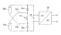
- FIG. 1there is shown a structure of an inverter circuit according to the invention.
- the photovoltaic generator which forms the DC sourceis divided into two (partial) strings 10 a , 10 b which each provide a DC voltage.
- the first and second DC sources 10 a , 10 bare preferably symmetrical, that is to say they generate essentially the same DC voltage in order to achieve the best results.
- the voltage in each string 10 a , 10 b at full loadis typically in the range between approximately 50% and approximately 100% of the intermediate circuit voltage. This achieves an input voltage range of approximately 1:2 at full load.
- the division of a photovoltaic generator 10 into two partial strings 10 a and 10 bis not a restriction in higher-power inverters since a plurality of identical partial strings are usually connected in parallel anyway.
- Both DC sources 10 a , 10 bare connected to a common step-up converter 12 - 16 , downstream of which an intermediate circuit capacitor 18 , also referred to as a link capacitor 18 , and finally an inverter 20 are connected.
- the common step-up converter 12 - 16contains a series circuit which has a first inductor 12 a and a first diode 16 a and is connected between an output of the first DC source 10 a and one side of the intermediate circuit capacitor 18 as well as a series circuit which has a second inductor 12 b and a second diode 16 b and is connected between an output of the second DC source 10 b and another side of the intermediate circuit capacitor 18 .
- the common step-up converter 12 - 16also contains a common circuit-breaker 14 which is connected between the first and second DC sources 10 a , 10 b in such a manner that it is connected between the connection between the first inductor 12 a and the first diode 16 a and the connection between the second inductor 12 b and the second diode 16 b .
- the two DC sources 10 a , 10 bare in series when the circuit-breaker 14 is closed and are in parallel when the switch 14 is open via the first and second diodes 16 a , 16 b .
- energyis delivered into the intermediate circuit capacitor 18 both when the circuit-breaker 14 is closed and when the circuit-breaker 14 is open.
- the energy which must be buffered in the inductors 12 a , 12 b of the step-up converter 12 - 16 or the reactive power circulating in the step-up converteris considerably smaller. Consequently, the two inductors 12 a , 12 b must be only approximately half as large and the load on the circuit-breaker 14 and also other semiconductor components is reduced. The losses in the step-up converter are considerably reduced, the overall efficiency of the inverter circuit is greater and the cooling capacity required is lower.
- the circuit-breaker 14If the DC voltage in the two strings 10 a , 10 b is approximately 50% or approximately 100% of the desired intermediate circuit voltage, a static series or parallel connection of the two DC sources 10 a , 10 b suffices to generate the intermediate circuit voltage. No switching losses are therefore produced in the circuit-breaker 14 . If the DC voltages in the two strings 10 a , 10 b are each in the range between approximately 50% and 100% of the intermediate circuit voltage, the circuit-breaker 14 is operated in a clocked manner. The duty ratio is controlled using a controller (not illustrated, analog or digital, for example a conventional PWM control circuit) in such a manner that the desired intermediate circuit voltage is produced. The duty ratio may vary between 100% (that is to say static series connection of 10 a and 10 b ) and 0% (that is to say static parallel connection of 10 a and 10 b ).
- FIG. 2shows a comparison of the efficiencies of the step-up converters against the DC voltages provided by the current sources.
- the overall efficiencies of the step-up converters 12 - 16 for the conventional circuit configuration from FIG. 4 (shown as the lower curve ⁇ in FIG. 2 ) and for the circuit configuration from FIG. 1 (shown as the upper curve ⁇ in FIG. 2 )are plotted for the operating conditions of full load, a constant clock frequency of the circuit-breaker 14 and an intermediate circuit voltage of 700 volts.
- the overall efficiency of the modified conventional circuit configuration from FIG. 5is somewhat below that from FIG. 4 .
- the step-up converter 12 - 16is not clocked, as a result of which the switching losses of the circuit-breaker 14 are omitted in both cases.
- thisis also possible at a DC voltage of 350 volts as a result of the static series connection of the two partial strings 10 a , 10 b.
- FIG. 2clearly shows that the efficiency of the step-up converter and thus also the overall efficiency of the inverter circuit could be considerably improved by the circuit configuration from FIG. 1 with a small outlay on components.
- the dependence of the efficiency or the losses of the step-up converter on the DC voltage provided by the photovoltaic generator 10is considerably smaller.
- the circuit-breaker 14can be driven either at a fixed or at a variable frequency. If the DC voltage in the partial strings 10 a , 10 b is in the vicinity of 50% or 100% of the intermediate circuit voltage, the clock frequency of the circuit-breaker 14 can be reduced, for example, in order to reduce the switching losses.
- the step-up converteris preferably not clocked but rather the two DC sources 10 a , 10 b are operated in a manner statically connected in parallel or in series. With such static operation, the semiconductors can be bridged with a relay, for example, in order to increase the efficiency further.
- the step-up converter 12 - 16may also be constructed from two or more branches which operate in a parallel manner and possibly with a phase offset (multiphase operation). In this case, individual branches may be entirely disconnected in the event of a partial load in order to increase the partial load efficiency.
- ring-around networksmay optionally be installed (resonant switching).
- step-up converters 12 - 16may also be connected in parallel or in series at the input of the inverter 20 .
- Half-bridgesfor single-phase supply
- three-phase bridgesare suitable, for example.
- first and second DC sources 10 a , 10 bmay also be used for the first and second DC sources 10 a , 10 b .
- fuel cells, thermoelectric generators, electromagnetic generators, rechargeable batteries, super-capacitors and the likeare also suitable as DC sources of the circuit configuration according to the invention.
- FIG. 3Another exemplary embodiment of a circuit configuration according to the invention is explained in more detail below with reference to FIG. 3 .
- identical or corresponding componentsare denoted using the same reference numerals as in the circuit configuration from FIG. 1 .
- the circuit configuration in this exemplary embodimentdiffers from the circuit configuration, as shown in FIG. 1 , in that two circuit-breakers 14 a and 14 b are connected between the first and second DC sources 10 a , 10 b , more precisely between the connection between the first inductor 12 a and the first diode 16 a and the connection between the second inductor 12 b and the second diode 16 b .
- the common switching element 14 of the common step-up converter 12 - 16is formed by two circuit-breakers 14 a , 14 b.
- the intermediate circuit capacitor 18is also formed from two capacitances 18 a and 18 b connected in series.
- connection between the two circuit-breakers 14 a , 14 bis connected in an electrically conductive manner to a connection between the two capacitances 18 a , 18 b .
- the inverter 20is additionally connected to the center tap between the two capacitances 18 a , 18 b.
- the voltage load on the semiconductor components used in the circuit configurationcan be halved in this manner. This in turn allows even better efficiency of the inverter circuit if the components are selected in a correspondingly suitable manner.
- the two circuit-breakers 14 a , 14 bmay be synchronously clocked.
- the two inductors 12 a , 12 bmay be either separate or coupled.
- This variantexhibits a similar behavior to the circuit configuration from FIG. 1 having only one circuit-breaker 14 .
- additional mutual influence with the inverter 20is obtained via the center tap between the two capacitances 18 a , 18 b.
- the two circuit-breakers 14 a and 14 bare clocked separately and the two inductors 12 a and 12 b are also separate.
- asymmetryoccurs between the voltages provided by the two capacitances 18 a , 18 b of the intermediate circuit capacitor, which asymmetry must be compensated for by the downstream inverter 20 .
- the maximum permissible asymmetrydepends on the photovoltaic voltage in the strings 10 a , 10 b and the ability of the inverter 20 to stabilize the neutral point between the two capacitances 18 a , 18 b.
- step-up converter circuit 12 - 16can also be configured for this situation without any problems even if the improvement in the efficiency diminishes with increasing asymmetry.
- circuit-breakers 14 a , 14 b and two capacitances 18 a , 18 bare used for the common switching element and the intermediate circuit capacitor, respectively, in the exemplary embodiment from FIG. 3 , it is likewise possible to respectively use three, four or more of these components.
- the circuit configuration of the inventioncan advantageously also be used, for example, to directly supply DC loads or to supply DC voltage intermediate circuits in other devices, for example motor frequency converters.
Landscapes
- Engineering & Computer Science (AREA)
- Power Engineering (AREA)
- Dc-Dc Converters (AREA)
- Inverter Devices (AREA)
Abstract
Description
Claims (14)
Priority Applications (1)
| Application Number | Priority Date | Filing Date | Title |
|---|---|---|---|
| US13/080,791US9042145B2 (en) | 2010-01-29 | 2011-04-06 | Circuit configuration with a step-up converter, and inverter circuit having such a circuit configuration |
Applications Claiming Priority (5)
| Application Number | Priority Date | Filing Date | Title |
|---|---|---|---|
| DE102010006124 | 2010-01-29 | ||
| DE102010006124.7 | 2010-01-29 | ||
| DE102010006124.7ADE102010006124B4 (en) | 2010-01-29 | 2010-01-29 | Circuit arrangement with a boost converter and inverter circuit with such a circuit arrangement |
| US13/017,060US8929112B2 (en) | 2010-01-29 | 2011-01-31 | Circuit arrangement having a boost converter, and inverter circuit having such a circuit arrangement |
| US13/080,791US9042145B2 (en) | 2010-01-29 | 2011-04-06 | Circuit configuration with a step-up converter, and inverter circuit having such a circuit configuration |
Related Parent Applications (1)
| Application Number | Title | Priority Date | Filing Date |
|---|---|---|---|
| US13/017,060Continuation-In-PartUS8929112B2 (en) | 2010-01-29 | 2011-01-31 | Circuit arrangement having a boost converter, and inverter circuit having such a circuit arrangement |
Publications (2)
| Publication Number | Publication Date |
|---|---|
| US20110188277A1 US20110188277A1 (en) | 2011-08-04 |
| US9042145B2true US9042145B2 (en) | 2015-05-26 |
Family
ID=44341527
Family Applications (1)
| Application Number | Title | Priority Date | Filing Date |
|---|---|---|---|
| US13/080,791Active2031-09-19US9042145B2 (en) | 2010-01-29 | 2011-04-06 | Circuit configuration with a step-up converter, and inverter circuit having such a circuit configuration |
Country Status (1)
| Country | Link |
|---|---|
| US (1) | US9042145B2 (en) |
Cited By (4)
| Publication number | Priority date | Publication date | Assignee | Title |
|---|---|---|---|---|
| US9397497B2 (en) | 2013-03-15 | 2016-07-19 | Ampt, Llc | High efficiency interleaved solar power supply system |
| US9438037B2 (en) | 2007-10-15 | 2016-09-06 | Ampt, Llc | Systems for optimized solar power inversion |
| US9442504B2 (en) | 2009-04-17 | 2016-09-13 | Ampt, Llc | Methods and apparatus for adaptive operation of solar power systems |
| US9466737B2 (en) | 2009-10-19 | 2016-10-11 | Ampt, Llc | Solar panel string converter topology |
Families Citing this family (2)
| Publication number | Priority date | Publication date | Assignee | Title |
|---|---|---|---|---|
| DE102010017747A1 (en)* | 2010-05-03 | 2011-11-03 | Sma Solar Technology Ag | Method for limiting the generator voltage of a photovoltaic system in case of danger and photovoltaic system |
| CN104104248B (en)* | 2014-06-20 | 2016-10-12 | 郑州大学 | Dual power supply photovoltaic DC-to-AC converter and control method thereof |
Citations (15)
| Publication number | Priority date | Publication date | Assignee | Title |
|---|---|---|---|---|
| US3459957A (en) | 1967-07-19 | 1969-08-05 | Ite Imperial Corp | Voltage regulator circuit |
| US6747881B2 (en)* | 2001-09-04 | 2004-06-08 | Semikron Elektronik Gmbh | Frequency converter |
| US20040165408A1 (en)* | 2003-02-21 | 2004-08-26 | Mr.Rick West | Dc to ac inverter with single-switch bipolar boost circuit |
| US20050068010A1 (en)* | 2003-09-30 | 2005-03-31 | Yaow-Ming Chen | Dual input DC-DC power converter integrating high/low voltage sources |
| US20050174817A1 (en)* | 2004-02-09 | 2005-08-11 | Heribert Schmidt | DC/AC converter to convert direct electric voltage into alternating voltage or into alternating current |
| US6963497B1 (en) | 2001-09-04 | 2005-11-08 | Edward Herbert | Power converter with an inductor input and switched capacitor outputs |
| US20050270816A1 (en)* | 2002-01-22 | 2005-12-08 | American Power Conversion Demark, Aps | Combined AC-DC to DC converter |
| DE102004037446A1 (en) | 2004-08-02 | 2006-06-01 | Conergy Ag | Transformerless inverter, for the conversion of solar direct current into sinusoidal alternating current for mains supply |
| WO2006106417A1 (en) | 2005-04-08 | 2006-10-12 | Meta System Spa | Circuit for the generation of two symmetrical buses of tension with respect to the negative of the feeding tension |
| US7138730B2 (en)* | 2002-11-22 | 2006-11-21 | Virginia Tech Intellectual Properties, Inc. | Topologies for multiple energy sources |
| DE102006014780A1 (en) | 2006-03-29 | 2007-10-18 | Schekulin, Ulrich | Direct current regulator for integrated network coupling of photovoltaic generator, has single or multi-phase transformer less inverter provided for coupling photovoltaic generator at direct current voltage intermediate circuit |
| EP2001111A2 (en) | 2006-03-29 | 2008-12-10 | Mitsubishi Denki Kabushiki Kaisha | Power supply apparatus |
| US20100072819A1 (en)* | 2008-09-22 | 2010-03-25 | Ablerex Electronics Co., Ltd | Bi-directional DC to DC power converter having a neutral terminal |
| DE102008050402A1 (en) | 2008-10-04 | 2010-04-08 | Diehl Ako Stiftung & Co. Kg | Circuit arrangement with a boost converter and inverter circuit with such a circuit arrangement |
| US8648497B2 (en)* | 2009-01-30 | 2014-02-11 | Renewable Power Conversion, Inc. | Photovoltaic power plant with distributed DC-to-DC power converters |
- 2011
- 2011-04-06USUS13/080,791patent/US9042145B2/enactiveActive
Patent Citations (17)
| Publication number | Priority date | Publication date | Assignee | Title |
|---|---|---|---|---|
| US3459957A (en) | 1967-07-19 | 1969-08-05 | Ite Imperial Corp | Voltage regulator circuit |
| US6747881B2 (en)* | 2001-09-04 | 2004-06-08 | Semikron Elektronik Gmbh | Frequency converter |
| US6963497B1 (en) | 2001-09-04 | 2005-11-08 | Edward Herbert | Power converter with an inductor input and switched capacitor outputs |
| US20050270816A1 (en)* | 2002-01-22 | 2005-12-08 | American Power Conversion Demark, Aps | Combined AC-DC to DC converter |
| US7138730B2 (en)* | 2002-11-22 | 2006-11-21 | Virginia Tech Intellectual Properties, Inc. | Topologies for multiple energy sources |
| US20040165408A1 (en)* | 2003-02-21 | 2004-08-26 | Mr.Rick West | Dc to ac inverter with single-switch bipolar boost circuit |
| US20050068010A1 (en)* | 2003-09-30 | 2005-03-31 | Yaow-Ming Chen | Dual input DC-DC power converter integrating high/low voltage sources |
| US20050174817A1 (en)* | 2004-02-09 | 2005-08-11 | Heribert Schmidt | DC/AC converter to convert direct electric voltage into alternating voltage or into alternating current |
| DE102004037446A1 (en) | 2004-08-02 | 2006-06-01 | Conergy Ag | Transformerless inverter, for the conversion of solar direct current into sinusoidal alternating current for mains supply |
| WO2006106417A1 (en) | 2005-04-08 | 2006-10-12 | Meta System Spa | Circuit for the generation of two symmetrical buses of tension with respect to the negative of the feeding tension |
| US7741817B2 (en) | 2005-04-08 | 2010-06-22 | Meta Systems S.P.A. | Circuit for the generation of two symmetrical buses of tension with respect to the negative of the feeding tension |
| DE102006014780A1 (en) | 2006-03-29 | 2007-10-18 | Schekulin, Ulrich | Direct current regulator for integrated network coupling of photovoltaic generator, has single or multi-phase transformer less inverter provided for coupling photovoltaic generator at direct current voltage intermediate circuit |
| EP2001111A2 (en) | 2006-03-29 | 2008-12-10 | Mitsubishi Denki Kabushiki Kaisha | Power supply apparatus |
| US7646182B2 (en) | 2006-03-29 | 2010-01-12 | Mitsubishi Electric Corporation | Power supply apparatus |
| US20100072819A1 (en)* | 2008-09-22 | 2010-03-25 | Ablerex Electronics Co., Ltd | Bi-directional DC to DC power converter having a neutral terminal |
| DE102008050402A1 (en) | 2008-10-04 | 2010-04-08 | Diehl Ako Stiftung & Co. Kg | Circuit arrangement with a boost converter and inverter circuit with such a circuit arrangement |
| US8648497B2 (en)* | 2009-01-30 | 2014-02-11 | Renewable Power Conversion, Inc. | Photovoltaic power plant with distributed DC-to-DC power converters |
Cited By (25)
| Publication number | Priority date | Publication date | Assignee | Title |
|---|---|---|---|---|
| US12003110B2 (en) | 2007-10-15 | 2024-06-04 | Ampt, Llc | Optimized conversion system |
| US11289917B1 (en) | 2007-10-15 | 2022-03-29 | Ampt, Llc | Optimized photovoltaic conversion system |
| US11070062B2 (en) | 2007-10-15 | 2021-07-20 | Ampt, Llc | Photovoltaic conversion systems |
| US12027869B2 (en) | 2007-10-15 | 2024-07-02 | Ampt, Llc | Optimized photovoltaic conversion configuration |
| US9673630B2 (en) | 2007-10-15 | 2017-06-06 | Ampt, Llc | Protected conversion solar power system |
| US12027867B2 (en) | 2007-10-15 | 2024-07-02 | Ampt, Llc | Coordinated converter reactively altering disabling photovoltaic electrical energy power system |
| US9438037B2 (en) | 2007-10-15 | 2016-09-06 | Ampt, Llc | Systems for optimized solar power inversion |
| US11070063B2 (en) | 2007-10-15 | 2021-07-20 | Ampt, Llc | Method for alternating conversion solar power |
| US11228182B2 (en) | 2007-10-15 | 2022-01-18 | Ampt, Llc | Converter disabling photovoltaic electrical energy power system |
| US10608437B2 (en) | 2007-10-15 | 2020-03-31 | Ampt, Llc | Feedback based photovoltaic conversion systems |
| US10326283B2 (en) | 2007-10-15 | 2019-06-18 | Ampt, Llc | Converter intuitive photovoltaic electrical energy power system |
| US10886746B1 (en) | 2007-10-15 | 2021-01-05 | Ampt, Llc | Alternating conversion solar power system |
| US10938219B2 (en) | 2009-04-17 | 2021-03-02 | Ampt, Llc | Dynamic methods and apparatus for adaptive operation of solar power systems |
| US10326282B2 (en) | 2009-04-17 | 2019-06-18 | Ampt, Llc | Safety methods and apparatus for adaptive operation of solar power systems |
| US9442504B2 (en) | 2009-04-17 | 2016-09-13 | Ampt, Llc | Methods and apparatus for adaptive operation of solar power systems |
| US11411126B2 (en) | 2009-10-19 | 2022-08-09 | Ampt, Llc | DC power conversion circuit |
| US10714637B2 (en) | 2009-10-19 | 2020-07-14 | Ampt, Llc | DC power conversion circuit |
| US10032939B2 (en) | 2009-10-19 | 2018-07-24 | Ampt, Llc | DC power conversion circuit |
| US9466737B2 (en) | 2009-10-19 | 2016-10-11 | Ampt, Llc | Solar panel string converter topology |
| US12034087B2 (en) | 2009-10-19 | 2024-07-09 | Ampt, Llc | Solar panel power conversion circuit |
| US11121556B2 (en) | 2013-03-15 | 2021-09-14 | Ampt, Llc | Magnetically coupled solar power supply system for battery based loads |
| US9397497B2 (en) | 2013-03-15 | 2016-07-19 | Ampt, Llc | High efficiency interleaved solar power supply system |
| US11967653B2 (en) | 2013-03-15 | 2024-04-23 | Ampt, Llc | Phased solar power supply system |
| US10116140B2 (en) | 2013-03-15 | 2018-10-30 | Ampt, Llc | Magnetically coupled solar power supply system |
| US12057514B2 (en) | 2013-03-15 | 2024-08-06 | Ampt, Llc | Converter controlled solar power supply system for battery based loads |
Also Published As
| Publication number | Publication date |
|---|---|
| US20110188277A1 (en) | 2011-08-04 |
Similar Documents
| Publication | Publication Date | Title |
|---|---|---|
| US8929112B2 (en) | Circuit arrangement having a boost converter, and inverter circuit having such a circuit arrangement | |
| Hu et al. | Power decoupling techniques for micro-inverters in PV systems-a review | |
| US8737093B1 (en) | Power converter with quasi-resonant voltage multiplier having shared switching node | |
| US9041251B2 (en) | Boost converter with multiple inputs and inverter circuit | |
| JP5783490B2 (en) | Power inverter with multiple supply on-board power supply | |
| US7929325B2 (en) | High efficiency, multi-source photovoltaic inverter | |
| KR101314975B1 (en) | Separating circuit for inverters | |
| US9806622B2 (en) | Power conversion device and power conversion control method for the same | |
| US9479075B2 (en) | Multilevel converter system | |
| US9042145B2 (en) | Circuit configuration with a step-up converter, and inverter circuit having such a circuit configuration | |
| WO2018023695A1 (en) | High-efficiency switched-capacitor power supplies and methods | |
| US20130272032A1 (en) | Dc/dc voltage converter and method for operating a dc/dc voltage converter | |
| US20140056044A1 (en) | Photovoltaic inverter and a control method thereof | |
| CN103119840B (en) | Bidirectional DC regulator | |
| US20120113694A1 (en) | Step-down converter and inverter circuit | |
| JP2013543193A5 (en) | ||
| US20130038130A1 (en) | Dc-to-ac converter system and dc-to-ac converter circuit | |
| Alassi et al. | Assessment of isolated and non-isolated DC-DC converters for medium-voltage PV applications | |
| US8711590B2 (en) | Circuit and method for generating an AC voltage from a plurality of voltage sources having a temporally variable DC output voltage | |
| EP2517345B1 (en) | Groundable dc/dc converter | |
| US10641245B2 (en) | Hybrid power generation system and an associated method thereof | |
| Hu et al. | Simple switched-capacitor-boost converter with large DC gain and low voltage stress on switches | |
| US10305287B2 (en) | Method for operating a photovoltaic system | |
| KR20160047131A (en) | Three-phase inverter and power converting apparatus in generation system | |
| US11283364B2 (en) | Power supply and power system having a step-down circuit and an inverse-conversion circuit |
Legal Events
| Date | Code | Title | Description |
|---|---|---|---|
| AS | Assignment | Owner name:DIEHL AKO STIFTUNG & CO. KG, GERMANY Free format text:ASSIGNMENT OF ASSIGNORS INTEREST;ASSIGNOR:SCHILL, CHRISTOPH;REEL/FRAME:030475/0897 Effective date:20110405 | |
| AS | Assignment | Owner name:PLATINUM GMBH, GERMANY Free format text:ASSIGNMENT OF ASSIGNORS INTEREST;ASSIGNOR:DIEHL AKO STIFTUNG & CO. KG;REEL/FRAME:035475/0160 Effective date:20150302 | |
| STCF | Information on status: patent grant | Free format text:PATENTED CASE | |
| AS | Assignment | Owner name:SEW-EURODRIVE GMBH & CO. KG, GERMANY Free format text:ASSIGNMENT OF ASSIGNORS INTEREST;ASSIGNOR:PLATINUM GMBH;REEL/FRAME:041768/0968 Effective date:20170123 | |
| MAFP | Maintenance fee payment | Free format text:PAYMENT OF MAINTENANCE FEE, 4TH YEAR, LARGE ENTITY (ORIGINAL EVENT CODE: M1551); ENTITY STATUS OF PATENT OWNER: LARGE ENTITY Year of fee payment:4 | |
| MAFP | Maintenance fee payment | Free format text:PAYMENT OF MAINTENANCE FEE, 8TH YEAR, LARGE ENTITY (ORIGINAL EVENT CODE: M1552); ENTITY STATUS OF PATENT OWNER: LARGE ENTITY Year of fee payment:8 |