US9041365B2 - Multiple mode RF power converter - Google Patents
Multiple mode RF power converterDownload PDFInfo
- Publication number
- US9041365B2 US9041365B2US13/747,694US201313747694AUS9041365B2US 9041365 B2US9041365 B2US 9041365B2US 201313747694 AUS201313747694 AUS 201313747694AUS 9041365 B2US9041365 B2US 9041365B2
- Authority
- US
- United States
- Prior art keywords
- voltage
- supply
- power
- operational mode
- voltage level
- Prior art date
- Legal status (The legal status is an assumption and is not a legal conclusion. Google has not performed a legal analysis and makes no representation as to the accuracy of the status listed.)
- Active, expires
Links
- 230000033228biological regulationEffects0.000claimsabstractdescription79
- 239000003990capacitorSubstances0.000claimsdescription60
- 238000012937correctionMethods0.000claimsdescription56
- 230000004044responseEffects0.000claimsdescription55
- 238000006073displacement reactionMethods0.000claimsdescription53
- 230000008878couplingEffects0.000claims1
- 238000010168coupling processMethods0.000claims1
- 238000005859coupling reactionMethods0.000claims1
- 238000000034methodMethods0.000abstractdescription15
- 230000003321amplificationEffects0.000description76
- 238000003199nucleic acid amplification methodMethods0.000description76
- 230000008859changeEffects0.000description36
- 230000004913activationEffects0.000description16
- 239000004065semiconductorSubstances0.000description12
- UXFQFBNBSPQBJW-UHFFFAOYSA-N2-amino-2-methylpropane-1,3-diolChemical compoundOCC(N)(C)COUXFQFBNBSPQBJW-UHFFFAOYSA-N0.000description11
- 101150035093AMPD geneProteins0.000description11
- 230000009849deactivationEffects0.000description11
- 229920006227ethylene-grafted-maleic anhydridePolymers0.000description11
- PZWOGYWWDIXJIB-KQYNXXCUSA-N[(2r,3s,4r,5r)-5-(6-aminopurin-9-yl)-3,4-dihydroxyoxolan-2-yl]methoxy-fluorophosphinic acidChemical compoundC1=NC=2C(N)=NC=NC=2N1[C@@H]1O[C@H](COP(O)(F)=O)[C@@H](O)[C@H]1OPZWOGYWWDIXJIB-KQYNXXCUSA-N0.000description10
- 238000001914filtrationMethods0.000description10
- 125000003345AMP groupChemical group0.000description9
- 230000003247decreasing effectEffects0.000description8
- 238000004891communicationMethods0.000description6
- 101100346654Saccharomyces cerevisiae (strain ATCC 204508 / S288c) MSS2 geneProteins0.000description5
- 230000005540biological transmissionEffects0.000description5
- 230000000694effectsEffects0.000description5
- 238000004519manufacturing processMethods0.000description5
- 230000008569processEffects0.000description5
- 229920006395saturated elastomerPolymers0.000description5
- 239000000758substrateSubstances0.000description5
- 101001090865Homo sapiens 26S proteasome regulatory subunit 7Proteins0.000description4
- 101000828889Homo sapiens tRNA modification GTPase GTPBP3, mitochondrialProteins0.000description4
- 230000007423decreaseEffects0.000description4
- 102100023793tRNA modification GTPase GTPBP3, mitochondrialHuman genes0.000description4
- 238000010586diagramMethods0.000description3
- 230000010354integrationEffects0.000description3
- 238000012546transferMethods0.000description3
- 229910000530Gallium indium arsenideInorganic materials0.000description2
- 229910000577Silicon-germaniumInorganic materials0.000description2
- KXNLCSXBJCPWGL-UHFFFAOYSA-N[Ga].[As].[In]Chemical compound[Ga].[As].[In]KXNLCSXBJCPWGL-UHFFFAOYSA-N0.000description2
- 230000005856abnormalityEffects0.000description2
- FTWRSWRBSVXQPI-UHFFFAOYSA-Nalumanylidynearsane;gallanylidynearsaneChemical compound[As]#[Al].[As]#[Ga]FTWRSWRBSVXQPI-UHFFFAOYSA-N0.000description2
- 230000008901benefitEffects0.000description2
- 238000006243chemical reactionMethods0.000description2
- 230000000593degrading effectEffects0.000description2
- 230000005669field effectEffects0.000description2
- 238000012986modificationMethods0.000description2
- 230000004048modificationEffects0.000description2
- 230000003071parasitic effectEffects0.000description2
- JBRZTFJDHDCESZ-UHFFFAOYSA-NAsGaChemical compound[As]#[Ga]JBRZTFJDHDCESZ-UHFFFAOYSA-N0.000description1
- ZOXJGFHDIHLPTG-UHFFFAOYSA-NBoronChemical compound[B]ZOXJGFHDIHLPTG-UHFFFAOYSA-N0.000description1
- GYHNNYVSQQEPJS-UHFFFAOYSA-NGalliumChemical compound[Ga]GYHNNYVSQQEPJS-UHFFFAOYSA-N0.000description1
- GPXJNWSHGFTCBW-UHFFFAOYSA-NIndium phosphideChemical compound[In]#PGPXJNWSHGFTCBW-UHFFFAOYSA-N0.000description1
- OAICVXFJPJFONN-UHFFFAOYSA-NPhosphorusChemical compound[P]OAICVXFJPJFONN-UHFFFAOYSA-N0.000description1
- XUIMIQQOPSSXEZ-UHFFFAOYSA-NSiliconChemical compound[Si]XUIMIQQOPSSXEZ-UHFFFAOYSA-N0.000description1
- NINIDFKCEFEMDL-UHFFFAOYSA-NSulfurChemical compound[S]NINIDFKCEFEMDL-UHFFFAOYSA-N0.000description1
- LEVVHYCKPQWKOP-UHFFFAOYSA-N[Si].[Ge]Chemical compound[Si].[Ge]LEVVHYCKPQWKOP-UHFFFAOYSA-N0.000description1
- 230000003213activating effectEffects0.000description1
- 238000013459approachMethods0.000description1
- 229910052785arsenicInorganic materials0.000description1
- RQNWIZPPADIBDY-UHFFFAOYSA-Narsenic atomChemical compound[As]RQNWIZPPADIBDY-UHFFFAOYSA-N0.000description1
- 229910052790berylliumInorganic materials0.000description1
- ATBAMAFKBVZNFJ-UHFFFAOYSA-Nberyllium atomChemical compound[Be]ATBAMAFKBVZNFJ-UHFFFAOYSA-N0.000description1
- 229910052796boronInorganic materials0.000description1
- 230000001413cellular effectEffects0.000description1
- 238000013461designMethods0.000description1
- 238000001514detection methodMethods0.000description1
- 230000001627detrimental effectEffects0.000description1
- 239000002019doping agentSubstances0.000description1
- 239000000284extractSubstances0.000description1
- 229910052733galliumInorganic materials0.000description1
- 230000000977initiatory effectEffects0.000description1
- 230000007774longtermEffects0.000description1
- 239000000463materialSubstances0.000description1
- 230000010355oscillationEffects0.000description1
- 229910052698phosphorusInorganic materials0.000description1
- 239000011574phosphorusSubstances0.000description1
- 229910052710siliconInorganic materials0.000description1
- 239000010703siliconSubstances0.000description1
- 238000001228spectrumMethods0.000description1
- 229910052717sulfurInorganic materials0.000description1
- 239000011593sulfurSubstances0.000description1
- JBQYATWDVHIOAR-UHFFFAOYSA-NtellanylidenegermaniumChemical compound[Te]=[Ge]JBQYATWDVHIOAR-UHFFFAOYSA-N0.000description1
- 229910052714telluriumInorganic materials0.000description1
- PORWMNRCUJJQNO-UHFFFAOYSA-Ntellurium atomChemical compound[Te]PORWMNRCUJJQNO-UHFFFAOYSA-N0.000description1
- 230000001052transient effectEffects0.000description1
- 238000011144upstream manufacturingMethods0.000description1
Images


Classifications
- G—PHYSICS
- G05—CONTROLLING; REGULATING
- G05F—SYSTEMS FOR REGULATING ELECTRIC OR MAGNETIC VARIABLES
- G05F1/00—Automatic systems in which deviations of an electric quantity from one or more predetermined values are detected at the output of the system and fed back to a device within the system to restore the detected quantity to its predetermined value or values, i.e. retroactive systems
- G05F1/10—Regulating voltage or current
- G05F1/46—Regulating voltage or current wherein the variable actually regulated by the final control device is DC
- G05F1/468—Regulating voltage or current wherein the variable actually regulated by the final control device is DC characterised by reference voltage circuitry, e.g. soft start, remote shutdown
- H—ELECTRICITY
- H02—GENERATION; CONVERSION OR DISTRIBUTION OF ELECTRIC POWER
- H02M—APPARATUS FOR CONVERSION BETWEEN AC AND AC, BETWEEN AC AND DC, OR BETWEEN DC AND DC, AND FOR USE WITH MAINS OR SIMILAR POWER SUPPLY SYSTEMS; CONVERSION OF DC OR AC INPUT POWER INTO SURGE OUTPUT POWER; CONTROL OR REGULATION THEREOF
- H02M1/00—Details of apparatus for conversion
- H02M1/10—Arrangements incorporating converting means for enabling loads to be operated at will from different kinds of power supplies, e.g. from AC or DC
- H—ELECTRICITY
- H03—ELECTRONIC CIRCUITRY
- H03F—AMPLIFIERS
- H03F1/00—Details of amplifiers with only discharge tubes, only semiconductor devices or only unspecified devices as amplifying elements
- H03F1/02—Modifications of amplifiers to raise the efficiency, e.g. gliding Class A stages, use of an auxiliary oscillation
- H03F1/0205—Modifications of amplifiers to raise the efficiency, e.g. gliding Class A stages, use of an auxiliary oscillation in transistor amplifiers
- H03F1/0211—Modifications of amplifiers to raise the efficiency, e.g. gliding Class A stages, use of an auxiliary oscillation in transistor amplifiers with control of the supply voltage or current
- H03F1/0216—Continuous control
- H03F1/0222—Continuous control by using a signal derived from the input signal
- H03F1/0227—Continuous control by using a signal derived from the input signal using supply converters
- H—ELECTRICITY
- H03—ELECTRONIC CIRCUITRY
- H03F—AMPLIFIERS
- H03F1/00—Details of amplifiers with only discharge tubes, only semiconductor devices or only unspecified devices as amplifying elements
- H03F1/26—Modifications of amplifiers to reduce influence of noise generated by amplifying elements
- H—ELECTRICITY
- H03—ELECTRONIC CIRCUITRY
- H03F—AMPLIFIERS
- H03F3/00—Amplifiers with only discharge tubes or only semiconductor devices as amplifying elements
- H03F3/20—Power amplifiers, e.g. Class B amplifiers, Class C amplifiers
- H03F3/24—Power amplifiers, e.g. Class B amplifiers, Class C amplifiers of transmitter output stages
- H—ELECTRICITY
- H04—ELECTRIC COMMUNICATION TECHNIQUE
- H04B—TRANSMISSION
- H04B15/00—Suppression or limitation of noise or interference
- H04B15/005—Reducing noise, e.g. humm, from the supply
- H—ELECTRICITY
- H02—GENERATION; CONVERSION OR DISTRIBUTION OF ELECTRIC POWER
- H02M—APPARATUS FOR CONVERSION BETWEEN AC AND AC, BETWEEN AC AND DC, OR BETWEEN DC AND DC, AND FOR USE WITH MAINS OR SIMILAR POWER SUPPLY SYSTEMS; CONVERSION OF DC OR AC INPUT POWER INTO SURGE OUTPUT POWER; CONTROL OR REGULATION THEREOF
- H02M1/00—Details of apparatus for conversion
- H02M1/0067—Converter structures employing plural converter units, other than for parallel operation of the units on a single load
- H02M2001/0067—
- H—ELECTRICITY
- H03—ELECTRONIC CIRCUITRY
- H03F—AMPLIFIERS
- H03F2200/00—Indexing scheme relating to amplifiers
- H03F2200/351—Pulse width modulation being used in an amplifying circuit
- H—ELECTRICITY
- H03—ELECTRONIC CIRCUITRY
- H03F—AMPLIFIERS
- H03F2200/00—Indexing scheme relating to amplifiers
- H03F2200/451—Indexing scheme relating to amplifiers the amplifier being a radio frequency amplifier
- H—ELECTRICITY
- H03—ELECTRONIC CIRCUITRY
- H03F—AMPLIFIERS
- H03F2200/00—Indexing scheme relating to amplifiers
- H03F2200/504—Indexing scheme relating to amplifiers the supply voltage or current being continuously controlled by a controlling signal, e.g. the controlling signal of a transistor implemented as variable resistor in a supply path for, an IC-block showed amplifier
Definitions
- the disclosurerelates generally to radio frequency (RF) power converters.
- Radio frequency (RF) power convertersto generate one or more supply voltages to power RF circuitry. If an RF switching converter provides Envelope Tracking (ET) and/or Average Power Tracking (APT), a supply voltage level of the supply voltage may need to be controlled with adequate precision in order to provide adequate power performance and to prevent unwanted distortion. Specialized RF components may be provided in RF power converters to meet spectrum and power performance requirements in certain operational modes. Unfortunately, these specialized RF components require additional die area, and therefore increase manufacturing costs.
- Envelope TrackingEnvelope Tracking
- APTAverage Power Tracking
- an RF power converterincludes a switching circuit, a switching controller, an RF filter, and a power mode controller.
- the switching circuitis operable to receive a power source voltage, the switching circuit being switchable so as to generate a pulsed output voltage from the power source voltage.
- the RF filteris coupled to receive the pulsed output voltage from the switching circuit and is operable to convert the pulsed output voltage from the switching circuit into a supply voltage.
- the switching controlleris configured to switch the switching circuit so that the switching circuit generates the pulsed output voltage and modulates the supply voltage.
- the switching controlleris configured to switch the switching circuit so that the switching circuit generates the pulsed output voltage and adjusts the pulsed output voltage to drive an average DC supply voltage level of the supply voltage to a target average DC supply voltage level.
- the power mode controlleris configured to provide the switching controller in both the ET operational mode and the APT operational mode.
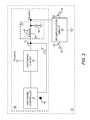
- FIG. 1illustrates one embodiment of a radio frequency (RF) switching converter with a switching controller and a switching circuit.
- RFradio frequency
- FIG. 2illustrates one embodiment of an RF amplification device with another embodiment of an RF switching converter and an RF amplification circuit where the RF switching converter has the switching controller and the switching circuit shown in FIG. 1 , along with an RF filter that converts a pulsed output voltage from the switching circuit into a supply voltage that is provided to the RF amplification circuit.
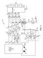
- FIG. 3is a semiconductor layout of one embodiment of the RF switching converter shown in FIG. 2 , where the RF switching converter includes a bang-bang controller (BBC), a voltage offset loop (VOL), a current sense detector, and an average frequency controller (AFC).
- BBCbang-bang controller
- VOLvoltage offset loop
- AFCaverage frequency controller
- FIG. 4illustrates one embodiment of the BBC shown in FIG. 3 , which compares a sense voltage level of a sense voltage to threshold voltage levels to operate the switching circuit shown in FIG. 3 .
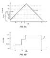
- FIG. 5Aillustrates one embodiment of the sense voltage as a function of time along with threshold voltage levels when the BBC shown in FIG. 4 is operating in a first bang-bang mode.
- FIG. 5Billustrates one embodiment of the pulsed output voltage generated by the switching circuit shown in FIG. 3 when the BBC shown in FIG. 4 is operating in the first bang-bang mode.
- FIG. 6Aillustrates one embodiment of the current sense signal as a function of time along with threshold voltage levels when the BBC is operating in a second bang-bang mode.
- FIG. 6Billustrates one embodiment of the pulsed output voltage generated by the switching circuit shown in FIG. 3 when the BBC shown in FIG. 4 is operating in the second bang-bang mode.
- FIG. 7Aillustrates one embodiment of the sense voltage as a function of time along with threshold voltage levels when the BBC shown in FIG. 4 is operating in a third bang-bang mode.
- FIG. 7Billustrates one embodiment of the pulsed output voltage generated by the switching circuit shown in FIG. 3 when the BBC shown in FIG. 4 is operating in the third bang-bang mode.
- FIG. 8Aillustrates one embodiment of the sense voltage as a function of time along with threshold voltage levels when the BBC shown in FIG. 4 is operating in a fourth bang-bang mode.
- FIG. 8Billustrates one embodiment of the pulsed output voltage generated by the switching circuit shown in FIG. 3 when the BBC shown in FIG. 4 is operating in the fourth bang-bang mode.
- FIG. 9illustrates one embodiment of the AFC shown in FIG. 3 , wherein the AFC sets a pulse count integer to an initial value and decrements the pulse count integer to a final value to determine whether an average pulse frequency of the pulsed output voltage is greater than or less than a target average frequency.
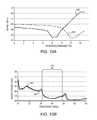
- FIG. 10Aillustrates a pair of noise curves for the RF switching converter shown in FIG. 3 , wherein the noise curves are each shown as a function of a threshold parameter when the target average frequency is 30 MHz.
- FIG. 10Billustrates a pair of wideband noise power curves for the RF switching converter shown in FIG. 3 , wherein the wideband noise power curves are functions of frequency.
- FIG. 11illustrates another embodiment of the AFC shown in FIG. 3 , wherein the AFC sets a pulse count integer to an initial value and increments the pulse count integer to a final value, and upper limits and lower limits for the final value are calculated to determine whether the average pulse frequency of the pulsed output voltage should be adjusted.
- FIG. 12illustrates still another embodiment of the AFC shown in FIG. 3 , wherein the AFC sets a pulse count integer to an initial value and increments the pulse count integer to a final value, and a gain error is used to adjust the average pulse frequency.
- FIG. 13illustrates one embodiment of the current sense detector shown in FIG. 3 , along with a ripple current correction circuit configured to generate a ripple correction current that reduces ripple variation in a supply current level of a supply current provided by the RF switching converter shown in FIG. 3 .
- FIG. 14illustrates one embodiment of the VOL illustrated in FIG. 3 wherein the VOL maintains a displacement voltage magnitude across a decoupling capacitor relatively constant.
- FIG. 15illustrates a graph of one embodiment of the supply voltage, a supply control output voltage, and the displacement voltage magnitude as a function of time.
- FIG. 16illustrates another embodiment of an RF amplification device.
- FIG. 17illustrates one embodiment of an RF power converter, which includes an RF switching converter, a low-drop out (LDO) regulation circuit, another LDO regulation circuit, and an RF filter that is configured to be alternated between different RF filter topologies.
- LDOlow-drop out
- FIG. 18is a circuit diagram illustrating an equivalent circuit topology when the LDO regulation circuit is activated.
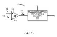
- FIG. 19illustrates one embodiment of the APT controller shown in FIG. 17 .
- FIG. 20Aillustrates one embodiment of the sense voltage as a function of time along with threshold voltage levels when the BBC shown in FIG. 4 is operating in a fifth bang-bang mode.
- FIG. 20Billustrates one embodiment of the pulsed output voltage generated by the switching circuit shown in FIG. 3 when the BBC shown in FIG. 4 is operating in the fifth bang-bang mode.
- FIG. 21Aillustrates one embodiment of the sense voltage as a function of time along with threshold voltage levels when the BBC shown in FIG. 4 is operating in a sixth bang-bang mode.
- FIG. 21Billustrates one embodiment of the pulsed output voltage generated by the switching circuit shown in FIG. 3 when the BBC shown in FIG. 4 is operating in the sixth bang-bang mode.
- FIG. 22is a graph illustrating system efficiency versus a target average power value.
- RF switching convertersconvert a power source voltage, such as a battery voltage, into a supply voltage.
- RF switching convertersare employed in RF power amplification devices to provide the supply voltage to an RF amplification circuit within the RF amplification device. Using this supply voltage, the RF amplification circuit amplifies an RF signal by transferring power from the supply voltage to the RF signal in accordance with an amplifier gain.
- the RF amplification devicesmay be used to amplify RF signals formatted in accordance with various RF communication standards.
- Different supply voltage biasing techniquesmay be more power efficient and/or introduce less distortion into the RF signal depending on the RF communication standard, power range, and/or RF frequency band.
- These supply voltage biasing techniquesmay include Envelope Tracking (ET), Average Power Tracking (APT), Polar Modulation, Low-Drop Out Regulation, and/or the like.
- Embodiments of the RF switching converters described hereinmay be designed to operate in different modes, where each mode is designed to implement a different supply voltage technique or a different set of supply voltage techniques.
- the RF switching convertersmay be designed to implement a different set of supply voltage techniques where each supply voltage technique in the set of supply voltage techniques provides a different supply voltage to different parts of the RF amplification circuit (such as driver amplifier stages and final amplifier stages).
- FIG. 1is a block diagram of one embodiment of an RF switching converter 10 .
- the RF switching converter 10has a switching controller 12 and a switching circuit 14 .
- the RF switching converter 10is configured to generate a pulsed output voltage 16 from a power source voltage V POWER .
- the power source voltage V POWERmay come from a power source, such as a battery, an AC-to-DC converter, and/or the like. Except for power source abnormalities and possibly AC-to-DC ripple variations, the power source voltage level of the power source voltage V POWER may generally be described as DC and relatively constant, at least with respect to some acceptable ripple variation and/or some acceptable rate of transient voltage abnormalities.
- the switching circuit 14is operable to receive the power source voltage V POWER .
- the switching circuit 14is switchable so as to generate the pulsed output voltage 16 from the power source voltage V POWER .
- the switching circuit 14may include one or more switches, such as switchable transistors, that can be turned on and turned off to present the pulsed output voltage 16 in at least two different voltage states. In this manner, pulses are produced in the pulsed output voltage 16 .
- the switching controller 12is configured to switch the switching circuit 14 and determine switch timing for proper regulation of the pulsed output voltage 16 .
- the switching controller 12may generate one or more control signals that turn on or turn off the switches and the switching circuit 14 .
- the switching controller 12may be analog, digital, and/or digital and analog, and may itself include various different controllers, as explained in further detail below.
- the pulsed output voltage 16may be transmitted to an RF filter to convert the pulsed output voltage 16 into a supply voltage.
- the RF filtermay or may not be included in the RF switching converter 10 .
- the RF filtermay instead be included within a power amplification circuit and be external to the RF switching converter 10 .
- the RF switching converter 10may be used to employ APT and ET supply voltage biasing techniques.
- OFDMAorthogonal frequency division multiple access multiplexing
- CDMAcode division multiple access multiplexing
- the switching controller 12is configured to switch the switching circuit 14 such that the pulsed output voltage 16 has an average pulse frequency.
- a duty ratio of the pulsed output voltage 16may vary, the duty ratio has an average value with respect to time, and thus the pulsed output voltage 16 has an average pulse frequency with respect to time.
- a DC supply voltage level of the supply voltageis determined by a pulse frequency of the pulsed output voltage 16 .
- a DC voltage state of the supply voltagevaries as the pulse frequency varies.
- the pulsed output voltage 16has an average pulse frequency, which is essentially the mean frequency at which pulses are provided in the pulsed output voltage 16 with respect to time. Nevertheless, due to manufacturing variations and operational variations (such as temperature variation and power source variation), the average pulse frequency of the pulsed output voltage 16 may not always be set consistently or in accordance with a contemplated design. In fact, in some embodiments, the average pulse frequency has been shown to change by up to ⁇ 40% due to operational variations.
- the switching controller 12is configured to adjust the average pulse frequency. As shown in FIG. 1 , the switching controller 12 is operable to receive a target average frequency value 18 .
- the target average frequency value 18is a data parameter that identifies a target average frequency for the average pulse frequency of the pulsed output voltage 16 .
- the switching controller 12is configured to detect that the average pulse frequency of the pulsed output voltage 16 during a time period differs from the target average frequency identified by the target average frequency value 18 .
- the switching controller 12reduces a difference between the average pulse frequency and the target average frequency identified by the target average frequency value 18 . In this manner, the switching controller 12 can eliminate, minimize, or at least decrease errors in the average pulse frequency of the pulsed output voltage 16 .
- the switching controller 12receives a pulsed feedback signal 20 that changes from one voltage state to another in accordance with the pulsed output voltage 16 generated by the switching circuit 14 .
- the pulses of the pulsed feedback signal 20are indicative of the pulses of the pulsed output voltage 16 .
- the switching controller 12can detect whether the average pulse frequency of the pulsed output voltage 16 differs from the target average frequency identified by the target average frequency value 18 during the time period. The switching controller 12 may then alter the switching frequency of the switching circuit 14 to reduce the difference between the average pulse frequency and the target average frequency identified by the target average frequency value 18 .
- the difference between the average pulse frequency and the target average frequencymay or may not be eliminated after a single time period.
- the switching controller 12may require multiple time periods in order to minimize the difference.
- the difference between the average pulse frequency and the target average frequency identified by the target average frequency value 18may or may not ever be fully eliminated. This may depend on the frequency resolution and the control accuracy of a particular embodiment of the RF switching converter 10 .
- FIG. 2illustrates one embodiment of an RF amplification device 22 .
- the RF amplification device 22includes another embodiment of an RF switching converter 24 and an RF amplification circuit 26 .
- the RF switching converter 24is the same as the RF switching converter 10 shown in FIG. 1 , except the RF switching converter 24 shown in FIG. 2 has an RF filter 28 coupled to receive the pulsed output voltage 16 .
- the RF switching converter 24has the same switching controller 12 and the same switching circuit 14 described above with respect to FIG. 1 .
- the RF filter 28is configured to convert the pulsed output voltage 16 from the switching circuit 14 into a supply voltage V SUPPLY for the RF amplification circuit 26 .
- the RF amplification circuit 26is operable to receive both the supply voltage V SUPPLY from the RF switching converter 24 and an RF signal 30 from external upstream RF circuitry.
- the RF amplification circuit 26receives the RF signal 30 at an input terminal 32 .
- the RF amplification circuit 26is configured to amplify the RF signal 30 using the supply voltage V SUPPLY from the RF switching converter 24 .
- the RF amplification circuit 26provides amplification to the RF signal 30 by transferring power from the supply voltage V SUPPLY to the RF signal 30 .
- the RF amplification circuit 26then outputs the RF signal 30 after amplification from an output terminal 34 to external downstream circuitry.
- the RF amplification circuit 26may be provided in a transmission chain of a transceiver in a user communication device, such as a laptop, a cellular phone, a tablet, a personal computer, or the like.
- the output terminal 34may be coupled to an antenna (not shown) that radiates the RF signal 30 to a base station or directly to another user communication device after amplification by the RF amplification circuit 26 .
- the RF amplification circuit 26may be configured to amplify the RF signal 30 when the RF signal 30 is formatted in accordance with any one of a multitude of RF communication standards. Often, the RF amplification circuit 26 is divided into RF amplification stages, including one or more driver RF amplification stages and a final RF amplification stage.
- the supply voltage V SUPPLYmay provide the supply voltage V SUPPLY to all of the RF amplification stages, or alternatively, to a set of the RF amplification stages. For example, the supply voltage V SUPPLY may provide the supply voltage V SUPPLY to only the final RF amplification stage.
- Other circuitrymay be provided in the RF switching converter 24 or externally to provide a second supply voltage to the driver RF amplification stages if desired.
- the RF signal 30may be encoded in any one of a plurality of multiplexing formats, such as Time Division Multiplexing (TDM), Frequency Division Multiplexing (FDM), CDMA, OFDMA, or the like.
- TDMTime Division Multiplexing
- FDMFrequency Division Multiplexing
- CDMACode Division Multiplexing
- the RF switching converter 24may be used to implement APT, and thus the RF amplification circuit 26 may need to be operated at back-off power levels well within a linear region of the RF amplification circuit 26 .
- the RF switching converter 24may be used to implement ET where the supply voltage level of the supply voltage V SUPPLY is modulated.
- Other types of power regulation circuits(either internal or external), such as low-drop out (LDO) regulation circuits, may be provided for TDM and FDM.
- LDOlow-drop out
- LDO regulation circuitsare generally unable to efficiently transfer power to the RF amplification circuit 26 for CDMA and OFDMA due to large resistances, which consume a significant amount of power.
- the RF switching converter 24is generally much more power efficient due to its ability to provide power conversion using primarily reactive components.
- the switching controller 12may be configured to switch the switching circuit 14 such that the RF amplification circuit 26 is configured to amplify the RF signal 30 when the RF signal 30 is formatted in accordance with a Long Term Evolution (LTE) standard, which utilizes OFDMA to encode data in the RF signal 30 .
- LTELong Term Evolution
- the RF amplification circuit 26needs to amplify the RF signal 30 without introducing an excessive amount of distortion into the RF signal 30 .
- the RF amplification circuit 26should operate near saturation. If the saturation voltage simply remains constant, the RF amplification circuit 26 introduces an excessive amount of distortion to the RF signal 30 , since the RF amplification circuit 26 is not operating linearly.
- the supply voltage V SUPPLYhas a supply voltage level that varies so as to adjust the saturation voltage of the RF amplification circuit 26 .
- the saturation voltage of the RF amplification circuit 26is selected so that the amplification gain associated with that saturation voltage is maintained essentially constant given the input power of the RF signal 30 .
- amplificationis provided linearly simply by selecting the saturation voltage so that the amplification gain remains essentially the same, regardless of the input power of the RF signal 30 .
- the RF filter 28is operable to receive the pulsed output voltage 16 from the switching circuit 14 , and is configured to convert the pulsed output voltage 16 into the supply voltage V SUPPLY .
- the RF filter 28includes a power inductor 36 coupled in series and a power capacitor 38 coupled in shunt with respect to the switching circuit 14 .
- the power inductor 36is configured to generate an inductor current 40 in response to the pulsed output voltage 16 . While the voltage across the power inductor 36 can change instantly, the power inductor 36 resists changes in the inductor current 40 . In contrast, while a current to the power capacitor 38 can change instantly, the power capacitor 38 resists changes in voltage.
- the supply voltage V SUPPLY in this embodimentis essentially the voltage across the power capacitor 38 .
- the power capacitor 38generates the supply voltage V SUPPLY having a supply voltage level that varies in accordance with a ripple variation.
- this ripple variationis generally small, and the RF filter 28 generates the supply voltage V SUPPLY with an average DC supply voltage level set in accordance with a pulse frequency of the pulsed output voltage 16 .
- the power inductor 36provides the inductor current 40 having an inductor current level that varies in accordance with a ripple variation.
- the ripple variationis generally small enough so that the inductor current 40 provides an average DC current level. As the pulse frequency varies, so does the average DC supply voltage level. In this manner, the supply voltage level is, for the most part, DC and can be set to a particular value by adjusting the pulse frequency of the pulsed output voltage 16 .
- the switching circuit 14is operable to receive the power source voltage V POWER , and is switchable so as to generate the pulsed output voltage 16 from the power source voltage V POWER .
- the switching controller 12is configured to switch the switching circuit 14 such that the pulsed output voltage 16 has an average pulse frequency.
- the average pulse frequencyis generally a center value for the pulse frequency. In this embodiment, the average pulse frequency may be set to different values, such as, for example, 5 MHz, 18 MHz, or 30 MHz.
- the pulse frequencymay vary from the average pulse frequency by ⁇ 4.5 MHz.
- the average pulse frequency(or, in other words, the center pulse frequency) may be set inappropriately or drift.
- the switching controller 12receives the pulsed feedback signal 20 and detects whether the average pulse frequency of the pulsed output voltage 16 differs from the target average frequency identified by the target average frequency value 18 during the time period. If so, the switching controller 12 adjusts the average pulse frequency to reduce the difference between the average pulse frequency and the target average frequency identified by the target average frequency value 18 .
- FIG. 3illustrates a semiconductor layout of one embodiment of the RF switching converter 24 , with the switching controller 12 , switching circuit 14 , and RF filter 28 shown in FIG. 2 .
- the RF switching converter 24 shown in FIG. 3includes a semiconductor substrate 42 .
- the switching controller 12 and the switching circuit 14are formed with the semiconductor substrate 42 .
- the switching controller 12 and the switching circuit 14may be formed in a device region formed from metallic layers and doped semiconductor layers in the semiconductor substrate 42 .
- Typical dopants that may be utilized to dope the semiconductor layers in the device region of the semiconductor substrate 42are Gallium (Ga), Arsenic (As), Silicon (Si), Tellurium (Te), Zinc (Zn), Sulfur (S), Boron (B), Phosphorus (P), Beryllium (Be), Aluminum Gallium Arsenide (AlGaAs), Indium Gallium Arsenide (InGaAs), and/or the like.
- the device regionis generally formed over a semiconductor die within the semiconductor substrate 42 .
- the semiconductor dieis generally not doped and can be formed from any suitable semiconductor material, such as Si, Silicon Germanium (SiGe), Gallium Arsenide (GaAs), Indium Phosphorus (InP), and/or the like.
- the switching controller 12 shown in FIG. 3includes a bang-bang controller (BBC) 44 , an average frequency controller (AFC) 46 , a current sense detector 48 , and a voltage offset loop (VOL) 50 .
- the switching controller 12is operable in a first operational mode, which in this example is an ET operational mode, and in a second operational mode, which in this example is an APT operational mode.
- the switching circuit 14includes a P-type field effect transistor (P-FET) 52 , an N-type field effect transistor (N-FET) 54 , and a charge pump 56 .
- the P-FET 52is operable to receive the power source voltage V POWER from a power source 58 , such as a battery.
- the N-FET 54is operable to receive a reference voltage, such as ground.
- the P-FET 52includes a source S P , a drain D P , and a gate G.
- the source S pis configured to receive the power source voltage V POWER .
- the N-FET 54includes a drain D N , a source S N , and a gate G N .
- the source S Nis coupled to ground, while the drain D N is coupled directly to the drain D P of the P-FET 52 .
- the pulsed output voltage 16is generated from a node N between the drain D P and the drain D N .
- the BBC 44 of the switching controller 12is configured to switch the P-FET 52 between an on state and an off state.
- the P-FET 52is configured to pull the pulsed output voltage 16 toward the power source voltage V POWER .
- the BBC 44is also configured to switch the N-FET 54 between the on state and the off state.
- the N-FET 54is configured to pull the pulsed output voltage 16 toward the reference voltage (i.e., ground) in the on state.
- the BBC 44is operable to generate a first control signal 60 that may be provided in an activation state or in a deactivation state.
- the first control signal 60is received at the gate G P of the P-FET 52 .
- the first control signal 60switches the P-FET 52 into the on state to pull the pulsed output voltage 16 toward the power source voltage V POWER .
- the P-FET 52is turned off and a power source voltage level of the power source voltage V POWER is dropped across the P-FET 52 .
- the BBC 44also generates a second control signal 62 .
- the gate G N of the N-FET 54is operable to receive the second control signal 62 from the BBC 44 .
- the N-FET 54is switched on and the pulsed output voltage 16 is pulled toward the reference voltage, in this case ground.
- the second control signal 62is in the deactivation state, the N-FET 54 is switched off and the voltage from the node N to the reference voltage is dropped across the N-FET 54 .
- the BBC 44is operable in a first bang-bang mode, in a second bang-bang mode, in a third bang-bang mode, in a fourth bang-bang mode, in a fifth bang-bang mode, and in a sixth bang-bang mode.
- the BBC 44only switches the P-FET 52 and the N-FET 54 on and off.
- the N-FET 54is switched off when the P-FET 52 is switched on.
- the pulsed output voltage 16is provided in a first voltage state near the power source voltage level (at voltage magnitude BUCK) of the power source voltage V POWER .
- the P-FET 52is switched off, the N-FET 54 is switched on.
- the pulsed output voltage 16is provided in a second voltage state near the reference voltage level of the reference voltage (in this case, near ground).
- the BBC 44may be set in the first bang-bang mode when the switching controller 12 is in the ET operational mode.
- the BBC 44may also be set in the first bang-bang mode when the switching controller 12 is in the APT operational mode.
- the BBC 44may be set in the first bang-bang mode during APT when the VOL 50 is activated and being used to generate an APT signal 73 .
- the BBC 44may be also be set in the first bang-bang mode if another APT signal is being used (such as an APT signal received by the switching controller 12 from external circuitry or an APT signal 280 (see below)).
- the BBC 44is also operable to control switches within the charge pump 56 .
- the charge pump 56has a switching topology that may include two flying capacitors and seven switches to allow the charge pump 56 to generate two different boost voltages that can be dynamically selected.
- the BBC 44while in the first bang-bang mode, the BBC 44 only switches the N-FET 54 and the P-FET 52 on and off to present step-down buck voltages at the node N.
- the BBC 44is further configured to operate the switches in the charge pump 56 so as to present two different boost voltage states, equal to about 1.5 times the power source voltage V POWER (i.e., the third voltage state) and 2 times the power source voltage V POWER (i.e., the fourth voltage state) at node N.
- the BBC 44may generate a charge pump output 64 , which may include several control signals to control the switches of the charge pump 56 .
- the BBC 44may switch the switching circuit 14 so that the pulsed output voltage 16 is provided at any of the four voltage states. The operation of the BBC 44 is explained in further detail below.
- the BBC 44may be set in the second bang-bang mode both when the switching controller 12 is in the ET operational mode and, if the VOL 50 is being used to generate the APT signal 73 , when the switching controller 12 is in the APT operational mode.
- the BBC 44is operable to control switches within the charge pump 56 .
- the BBC 44is configured to operate the switches of the charge pump 56 so that the pulsed output voltage 16 is provided only between the first voltage state and the third voltage state.
- the BBC 44may be set in the third bang-bang mode both when the switching controller 12 is in the ET operational mode and, if the VOL 50 is being used to generate the APT signal 73 , when the switching controller 12 is in the APT operational mode.
- the BBC 44is also operable to control switches within the charge pump 56 in the fourth bang-bang mode.
- the BBC 44is configured to operate the switches of the charge pump 56 so that the pulsed output voltage 16 is provided only between the third voltage state and the fourth voltage state.
- the BBC 44may be set in the fourth bang-bang mode both when the switching controller 12 is in the ET operational mode and, if the VOL 50 is being used to generate the APT signal 73 , when the switching controller 12 is in the APT operational mode.
- the BBC 44is configured to operate the switches of the charge pump 56 so that the pulsed output voltage 16 is provided only between the first voltage state and the third voltage state, as in the third bang-bang mode.
- the BBC 44uses the same thresholds as in the first bang-bang mode, as explained in further detail below.
- the fifth bang-bang modeis not used when the switching controller 12 is in the ET operational mode, or during the APT operational mode if the VOL 50 is being used to generate the APT signal 73 .
- the BBC 44is configured to operate the switches of the charge pump 56 so that the pulsed output voltage 16 is provided only between the third voltage state and the fourth voltage state, as in the fourth bang-bang mode.
- the BBC 44uses the same thresholds as in the first bang-bang mode, as explained in further detail below.
- the BBC 44may be set in the sixth bang-bang mode both when the switching controller 12 is in the ET operational mode and during the APT operational mode.
- the sixth bang-bang modeis not used when the switching controller 12 is in the ET operational mode or, if the VOL 50 is being used to generate the APT signal 73 , in the APT operational mode.
- the BBC 44receives a threshold parameter 66 from the AFC 46 .
- the AFC 46 of the switching controller 12is operable to receive the threshold parameter 66 at an initialized value from external circuitry.
- the BBC 44is also operable to receive an offset voltage 68 from the VOL 50 when the switching controller 12 is operating in the ET operational mode.
- the BBC 44is operable to receive a current sense signal 70 from the current sense detector 48 when the switching controller 12 is operating in the ET operational mode.
- the current sense signal 70has a signal level indicative of a current level of the inductor current 40 of the power inductor 36 .
- the current sense detector 48receives a feedback voltage 72 and generates the current sense signal 70 as a current having a current level indicative of the current level of the inductor current 40 in the ET operational mode.
- the BBC 44is configured to set the average pulse frequency of the pulsed output voltage 16 based on the threshold parameter 66 from the AFC 46 . To correct the average pulse frequency, the AFC 46 adjusts the threshold parameter 66 to reduce the difference between the average pulse frequency and the target average frequency identified by the target average frequency value 18 . After the time period for detection of the average pulse frequency, the AFC 46 adjusts the threshold parameter 66 and provides the updated threshold parameter 66 to the BBC 44 .
- the current sense detector 48 and the VOL 50are each operable to be activated and deactivated.
- the BBC 44is operable to receive the current sense signal 70 from the current sense detector 48 and the offset voltage 68 from the VOL 50 .
- the current sense detector 48 and the VOL 50are activated.
- the VOL 50is further operable in the ET operational mode and in the APT operational mode.
- the VOL 50is also configured to operate in the ET operational mode.
- the VOL 50is configured to generate the offset voltage 68 having an offset voltage magnitude, as explained above.
- the BBC 44is configured to switch the switching circuit 14 based on the current sense signal 70 and the offset voltage 68 so that the switching circuit 14 generates the pulsed output voltage 16 . More specifically, the BBC 44 is configured to switch the switching circuit 14 based on the sense signal level of the current sense signal 70 and the offset voltage magnitude of the offset voltage 68 so that the switching circuit 14 generates the pulsed output voltage 16 .
- the current sense detector 48is configured to generate the current sense signal 70 such that a derivative of the current sense signal 70 is negatively proportional to a derivative of the inductor current 40 (see FIG. 3 ), which is a supply current from the switching circuit 14 .
- a derivative of the supply voltage V SUPPLYacross the power capacitor 38 is directly proportional to the derivative of the inductor current 40
- the derivative of the current sense signal 70is also negatively proportional to a derivative of the supply voltage V SUPPLY .
- the VOL 50is configured to generate the current sense signal 70 such that a first change in the inductor current 40 (or in the supply voltage level of the supply voltage V SUPPLY ) results in a second change in the sense signal level, the second change being negatively proportional to the first change. Accordingly, the sense signal level of the current sense signal 70 increases as a result of the inductor current 40 (or supply voltage level of the supply voltage V SUPPLY ) decreasing and vice versa.
- the current sense signal 70is a sense current and the sense signal level is a current level of the sense current.
- the switching controller 12is also operable in the APT operational mode.
- the BBC 44is operable to receive the APT signal 73 and is configured to switch the switching circuit 14 based on an APT signal level of the APT signal 73 so that the switching circuit 14 generates the pulsed output voltage 16 .
- the current sense detector 48is deactivated and thus does not generate the current sense signal 70 .
- the VOL 50may be activated and also operate in the APT operational mode. The VOL 50 does not generate the offset voltage 68 in the APT operational mode. Rather, the VOL 50 is configured to generate the APT signal 73 in the APT operational mode.
- the APT signal 73is generated by the VOL 50 such that the APT signal level varies from a DC offset signal level of the APT signal in accordance with the ripple variation of the supply voltage level of the supply voltage V SUPPLY .
- the BBC 44is configured to switch the switching circuit 14 based on an APT signal level of the APT signal 73 in the APT operational mode so that the switching circuit 14 generates the pulsed output voltage 16 .
- the supply voltage level of the supply voltage V SUPPLYhas an average DC supply voltage level set in accordance with the DC offset signal level of the APT signal 73 in the APT operational mode.
- the VOL 50may be deactivated when the switching controller 12 is in the APT operational mode.
- the APT signal 73may be received from an internal or external APT controller, as explained in further detail below.
- the VOL 50is configured to generate the APT signal 73 such that a derivative of the APT signal 73 is negatively proportional to a derivative of the supply voltage V SUPPLY .
- the VOL 50is configured to generate the APT signal 73 such that a first change in the supply voltage level of the supply voltage V SUPPLY results in a second change in the APT signal level, the second change being negatively proportional to the first change.
- the APT signal levelincreases as a result of the supply voltage level decreasing, and vice versa.
- the APT signal 73is an APT voltage and the APT signal level is an APT voltage level.
- FIG. 4illustrates one embodiment of the BBC 44 shown in FIG. 3 .
- the BBC 44includes a digital control unit 74 , a decoder 76 , a comparator 80 , a comparator 82 , a comparator 84 , a comparator 86 , a voltage adder 88 , a voltage adder 90 , a voltage adder 92 , a voltage adder 94 , a voltage adder 96 , a voltage adder 98 , a variable resistor 100 , a variable resistor 102 , a mirrored ratio circuit 104 , and a multiplexer MUX 1 .
- the digital control unit 74is configured to receive the threshold parameter 66 from the AFC 46 (shown in FIG. 3 ).
- the BBC 44is configured to set a first threshold voltage level based on the threshold parameter 66 .
- the digital control unit 74searches a stored list of threshold magnitudes based on the threshold parameter 66 .
- is then used to generate a first intermediary current signal 106 and a second intermediary current signal 108 .
- the first intermediary current signal 106has a current level with a negative of the threshold magnitude, ⁇
- the first intermediary current signal 106is transmitted through the variable resistor 102 to provide a first intermediary voltage 110 .
- the first intermediary voltage 110is a voltage across the variable resistor 102 .
- the variable resistor 102has a variable resistance of R dac1 , which is set by the digital control unit 74 .
- the second intermediary current signal 108has a current level that is a positive of the threshold magnitude, +
- the second intermediary current signal 108is transmitted through the variable resistor 100 to generate a second intermediary voltage 112 .
- the second intermediary voltage 112is a voltage across the variable resistor 100 .
- the variable resistor 100has a variable resistance of R dac2 .
- the digital control unit 74is configured to set the variable resistance R dac2 .
- the variable resistances R dac1 , R dac2are set by the digital control unit 74 to the same, or substantially the same, resistance value.
- the decoder 76is configured to receive an operational mode control input 114 .
- the operational mode control input 114may include one or more bit signals in order to represent a word.
- the operational mode control input 114may indicate the first bang-bang mode, the second bang-bang mode, the third bang-bang mode, the fourth bang-bang mode, the fifth bang-bang mode, or the sixth bang-bang mode.
- the voltage adders 92 and 94are provided in order to add a range voltage 116 to the first intermediary voltage 110 and the second intermediary voltage 112 .
- the range voltage 116has a voltage level of zero (0) Volts.
- a first threshold signal 118is generated having a first threshold voltage level based on the threshold parameter 66 .
- a second threshold signal 120is generated having a second threshold voltage level based on the threshold parameter 66 .
- the first threshold voltage level and the second threshold voltage levelare used to determine when to turn on and turn off the P-FET 52 (shown in FIG. 3 ) and the N-FET 54 (shown in FIG. 3 ) in the first through fourth bang-bang modes.
- the first bang-bang modeonly the first threshold voltage level of the first threshold signal 118 and the second threshold voltage level of the second threshold signal 120 are relevant.
- the charge pump 56(shown in FIG. 3 ) is not utilized.
- additional threshold levels to set boost levelscan be provided through the operation of the charge pump 56 when the switching controller 12 is in the ET operational mode.
- both the first threshold signal 118 and the second threshold signal 120are voltages, and in particular, DC voltages.
- the first threshold voltage level of the first threshold signal 118 and the second threshold voltage level of the second threshold signal 120are relatively constant voltage levels.
- the second threshold voltage levelis lower than the first threshold voltage level because the first intermediary current signal 106 had the negative of the threshold magnitude, ⁇ 51 TM
- the first threshold signal 118is received at a non-inverting terminal of the comparator 84
- the second threshold signal 120is received at a non-inverting terminal of the comparator 86 .
- the current sense detector 48 and the VOL 50are both activated.
- the VOL 50is set to operate in the ET operational mode.
- the current sense signal 70is provided to the mirrored ratio circuit 104 .
- the mirrored ratio circuit 104has a variable resistor 104 A and a mirror circuit 104 B.
- the mirror circuit 104 Breceives the current sense signal 70 and is configured to generate a mirror current 104 C from the current sense signal 70 .
- the multiplexer MUX 1is configured to select the mirror current 104 C, and thus the current sense signal 70 , in response to a multiplexer select bit signal MX 1 being in a first bit state (i.e., logical “1” or logical “0”).
- the multiplexer select bit signal MX 1is provided in the first bit state so that the multiplexer MUX 1 selects the current sense signal 70 (i.e., through the mirror current 104 C) from the current sense detector 48 when the current sense detector 48 is activated.
- a ratio of a current level of the mirror current 104 C and the current level of the current sense signal 70is 1/M.
- the ratio 1/Mis variable where the value of M is controlled by the digital control unit 74 based on a dedicated MIPI bit 104 D.
- the first threshold voltage level and the second threshold voltage levelare set to equal the R dac (i.e., the resistance value of either R dac1 or R dac2 )/R*M*
- the value of Mis set equal to 20.
- the threshold parameter 66since the threshold parameter 66 is 4 bits, the threshold parameter 66 may represent current levels from 20 mA to 40 mA in steps of 2 mA.
- the second bang-bang moderequires an increased range. To increase the range for the second bang-bang mode, the value M is set equal to 40.
- the threshold parameter 66since the threshold parameter 66 is 4 bits, the threshold parameter may represent current levels from 40 mA to 80 mA in steps of 4 mA.
- the threshold parameter 66may thus represent current levels where the ratio of 1/M may be changed from 1/20 to 1/40 via the dedicated MIPI bit 104 D.
- a preliminary voltage 104 Ewhich is the voltage across the variable resistor 104 A, is then generated and provided to the voltage adder 96 .
- the variable resistor 104 Ahas a variable resistance R, which is set by the digital control unit 74 .
- the variable resistances R, R dac1 , R dac2are reduced so that R and R dac1 , and R and R dac2 , have the same ratio to allow an increased feedback dynamic range, and the decoder 76 operates in the second bang-bang mode.
- both the ratios for R and R dac1 , and R and R dac2are set back to their nominal values and the decoder 76 operates in the first bang-bang mode.
- the offset voltage 68is received at the voltage adder 98 from the VOL 50 , which adds the range voltage 116 so as to generate a preliminary voltage 122 .
- the preliminary voltage 122is subtracted from the preliminary voltage 104 E so as to generate a sense voltage 124 having a sense voltage level indicative of a current level of the current across the power inductor 36 (shown in FIG. 3 ) and the supply voltage level of the supply voltage V SUPPLY .
- the sense voltage 124is a voltage
- the current sense signal 70is a current.
- a clip 126provides voltage limitations to the sense voltage 124 to ensure that the appropriate headroom is provided to the P-FET 52 (shown in FIG. 3 ) and the N-FET 54 (shown in FIG. 3 ).
- the comparator 84generates a comparator signal 127 from the comparison of the sense voltage 124 and the first threshold signal 118 .
- the decoder 76turns on the P-FET 52 and turns off the N-FET 54 in response to the sense voltage level being above the first threshold voltage level.
- the decoder 76is configured to generate the first control signal 60 in the activation state and the second control signal 62 in the deactivation state.
- the comparator 86generates a comparator signal 128 , which is received by the decoder 76 .
- the comparator 86is configured to compare the second threshold voltage level and the sense voltage level of the sense voltage 124 .
- the decoder 76is configured to turn off the P-FET 52 and turn on the N-FET 54 in response to the sense voltage level of the sense voltage 124 being below the second threshold voltage level of the second threshold signal 120 .
- the decoder 76is configured to generate the first control signal 60 in the deactivation state and the second control signal 62 in the activation state.
- the BBC 44does not turn off the P-FET 52 and turn on the N-FET 54 when the sense voltage level is below the first threshold voltage level of the first threshold signal 118 . Rather, the P-FET 52 is turned off and the N-FET 54 is turned on in response to the sense voltage level being below the second threshold voltage level. This provides the so-called “bang-bang” control operation of the BBC 44 .
- the range voltage 116is also provided to provide a greater range for comparisons.
- the range voltage 116may have a range voltage level of approximately 1.7 volts in the second bang-bang mode.
- a third intermediary voltage 129is generated by the digital control unit 74 based on the threshold parameter 66 .
- a third threshold signal 130is generated from the voltage adder 90 having a third threshold voltage level.
- the BBC 44is configured to set a third threshold voltage level that is higher than the first threshold voltage level in the high voltage mode.
- the digital control unit 74is configured to generate a fourth intermediary voltage 132 based on the threshold parameter 66 in the high voltage mode.
- a fourth threshold signal 134is generated from the voltage adder 88 having a fourth threshold voltage level. In this manner, the BBC 44 is configured to set a fourth threshold voltage level that is higher than the third threshold voltage level.
- the comparator 82receives the third threshold signal 130 at a non-inverting input and the sense voltage 124 at an inverting input.
- a comparator signal 136is generated from the comparator 82 .
- the decoder 76is configured to switch the charge pump 56 (shown in FIG. 3 ) such that the pulsed output voltage 16 is provided in the first high voltage state (which, in this example, is approximately 1.5 times the power source voltage level of the power source voltage V POWER ) in response to the sense voltage level being above the third threshold voltage level of the third threshold signal 130 .
- the comparator 80is configured to receive the fourth threshold signal 134 at a non-inverting terminal and the sense voltage 124 at an inverting terminal.
- the comparator 80is configured to generate a comparator signal 138 .
- the decoder 76is configured to switch the charge pump 56 such that the pulsed output voltage 16 is provided in the second high voltage state (which, in this example, is approximately double the power source voltage level of the power source voltage V POWER ) in response to the sense voltage level being above the fourth threshold voltage level.
- the decoder 76is configured to control the charge pump 56 by controlling the activation and deactivation states of the control signals in the charge pump output 64 .
- FIG. 5Aillustrates one embodiment of the sense voltage 124 with respect to time.
- a voltage magnitude V OFFSis the magnitude of the offset voltage 68 received from the VOL 50 shown in FIG. 3 .
- the voltage magnitude V OFFSdetermines a center voltage level V CEN since the first intermediary current signal 106 was the negative of the threshold magnitude
- the second threshold voltage levelis provided at a voltage difference V I lower than the center voltage level V CEN .
- the second threshold voltage levelis thus at M 2 .
- the first threshold voltage level of the first threshold signal 118is provided at M 1 .
- the first threshold voltage level M 1is the voltage difference V I above the center voltage level V CEN .
- FIG. 5Billustrates one embodiment of the pulsed output voltage 16 in the first bang-bang mode.
- the voltage magnitude BUCK in FIG. 5Brepresents the voltage level resulting in the pulsed output voltage 16 when the P-FET 52 (shown in FIG. 3 ) is pulled up near the power source voltage level of the power source voltage V POWER (shown in FIG. 3 ).
- the voltage magnitude AG (i.e., approximately ground) in FIG. 5Brepresents the voltage level resulting in the pulsed output voltage 16 when the N-FET 54 (shown in FIG. 3 ) is pulled down near ground.
- the sense voltage level of the sense voltage 124is above the first threshold voltage level M 1 at time t 1 .
- the P-FET 52pulls the pulsed output voltage 16 to the voltage magnitude BUCK in response to the sense voltage level of the sense voltage 124 being above the first threshold voltage level M 1 , as shown in FIG. 5B .
- the pulsed output voltage 16is maintained at the voltage magnitude BUCK until time t 2 .
- the sense voltage level of the sense voltage 124is below the second threshold voltage level M 2 at time t 2 .
- the N-FET 54pulls the pulsed output voltage 16 to the voltage level AG in response to the sense voltage level of the sense voltage 124 being below the second threshold voltage level M 2 , as shown in FIG. 5B .
- the processrepeats itself to generate pulses 140 in the pulsed output voltage 16 .
- the BBC 44 shown in FIG. 3is thus configured to switch the switching circuit 14 at a switching frequency that is based on the threshold parameter 66 . This is because the threshold parameter 66 determines the voltage and the voltage difference V I , and thus determines how often and for how long a pulse 140 is provided in the pulsed output voltage 16 .
- FIG. 6A and FIG. 6Billustrate the operation of the BBC 44 shown in FIG. 3 in the second bang-bang mode. Note that in the second bang-bang mode, the first threshold voltage level M 1 and the second threshold voltage level M 2 have been adjusted downward by the range voltage level V CM of the range voltage 116 (shown in FIG. 4 ).
- the sense voltage 124is shown in FIG. 6A , along with the third threshold voltage level M 3 of the third threshold signal 130 and the fourth threshold voltage level M 4 of the fourth threshold signal 134 .
- the sense voltage level of the sense voltage 124is above the first threshold voltage level M 1 , as shown in FIG. 6A . Accordingly, in response, the pulsed output voltage 16 is pulled to the voltage magnitude BUCK, as shown in FIG. 6B . The voltage level of the pulsed output voltage 16 is maintained at the voltage magnitude BUCK until time t 4 . At time t 4 , the sense voltage level of the sense voltage 124 is above the third threshold voltage level M 3 , as shown in FIG. 6A . Accordingly, the BBC 44 switches the charge for the charge pump 56 so that the voltage level of the pulsed output voltage 16 is provided at the high voltage state of 1.5X, as shown in FIG. 6B .
- the voltage levelis maintained in the high voltage state 1.5X (i.e., the third voltage state) until time t 5 .
- the sense voltage level of the sense voltage 124is above the fourth threshold voltage level M 4 , as shown in FIG. 6A .
- the BBC 44operates the charge pump 56 so that the voltage level of the pulsed output voltage 16 is provided at the high voltage state 2.0X (i.e., the fourth voltage state), as shown in FIG. 6B .
- the voltage level of the pulsed output voltage 16is maintained at the high voltage state 2.0X until time t 6 .
- the sense voltage level of the sense voltage 124is below the second threshold voltage level M 2 , as shown in FIG. 6A .
- the voltage level of the pulsed output voltage 16is pulled down to the voltage level AG, as shown in FIG. 6B .
- the operation of the BBC 44 (shown in FIG. 3 ) in FIGS. 5A , 5 B, 6 A, and 6 Bhas been given, the operation of embodiments of the AFC 46 (shown in FIG. 3 ) can now be described.
- FIG. 7Aillustrates one embodiment of the sense voltage 124 with respect to time.
- the voltage magnitude V OFFSis the magnitude of the offset voltage 68 received from the VOL 50 shown in FIG. 3 .
- the threshold voltage levels M 1 , M 2 , M 3 , and M 4are the same as those in the second bang-bang mode. However, only the first threshold voltage level M 1 and the third threshold voltage level M 3 are relevant in the fourth bang-bang mode.
- FIG. 7Billustrates one embodiment of the pulsed output voltage 16 in the third bang-bang mode.
- the sense voltage level of the sense voltage 124is above the third threshold voltage level M 3 at time t 7 .
- the BBC 44operates the charge pump 56 so that the voltage level of the pulsed output voltage 16 is provided at the high voltage state 1.5X (i.e., the third voltage state), as shown in FIG. 7B .
- the pulsed output voltage 16is maintained at the third voltage state 1.5X until time t 8 .
- the sense voltage level of the sense voltage 124is below the first threshold voltage level M 1 at the time t 8 .
- the BBC 44operates the P-FET 52 so that the voltage level of the pulsed output voltage 16 is provided at the first voltage state with the voltage magnitude BUCK, as shown in FIG. 7B .
- the processrepeats itself at times t 9 and t 10 .
- FIG. 8Aillustrates one embodiment of the sense voltage 124 with respect to time.
- the voltage magnitude V OFFSis the magnitude of the offset voltage 68 received from the VOL 50 shown in FIG. 3 .
- the threshold voltage levels M 1 , M 2 , M 3 , and M 4are the same as those in the second bang-bang mode. However, only the fourth threshold voltage level M 4 and the third threshold voltage level M 3 are relevant in the fourth bang-bang mode.
- FIG. 8Billustrates one embodiment of the pulsed output voltage 16 in the fourth bang-bang mode.
- the sense voltage level of the sense voltage 124is above the fourth threshold voltage level M 4 at time t 11 .
- the BBC 44operates the charge pump 56 so that the voltage level of the pulsed output voltage 16 is provided at the high voltage state 2.0X (i.e., the fourth voltage state), as shown in FIG. 7B .
- the pulsed output voltage 16is maintained at the voltage state 2.0X until time t 12 .
- the sense voltage level of the sense voltage 124is below the third threshold voltage level M 3 at the time t 12 .
- the BBC 44operates the charge pump 36 so that the voltage level of the pulsed output voltage 16 is provided at the third voltage state with the 1.5X voltage magnitude, as shown in FIG. 8B .
- the processrepeats itself at times t 13 and t 14 .
- FIG. 9illustrates one embodiment of an AFC 46 ( 1 ).
- the AFC 46 ( 1 )includes a clock generation circuit 142 , a counter 144 , a digital control unit 146 , and an accumulator 148 .
- the clock generation circuit 142receives a pulse ratio parameter 150 that identifies a pulse ratio.
- the pulse ratio parameter 150may be an integer equal to one (1), two (2), or four (4).
- the clock generation circuit 142generates a clock signal from the pulsed feedback signal 20 . More specifically, the clock generation circuit 142 shown in FIG. 9 is configured to generate a clock signal 152 such that clock pulses of the clock signal 152 are provided at the pulse ratio with respect to the pulses 140 (shown in FIG.
- the pulse ratio identified by the pulse ratio parameter 150is one (1), for every pulse in the pulsed feedback signal 20 there is a clock pulse in the clock signal 152 .
- the pulse ratio parameter 150is two (2), the clock generation circuit 142 provides one clock pulse for every two pulses in the pulsed feedback signal 20 . If the pulse ratio identified by the pulse ratio parameter 150 is four (4), there will be four pulses in the pulsed feedback signal 20 for every clock pulse in the clock signal 152 .
- the clock generation circuit 142provides the clock signal 152 to the counter 144 .
- the counter 144is configured to perform a count operation on a pulse count integer during a time period in accordance with the clock signal 152 so that the pulse count integer has a final value upon expiration of the time period.
- the digital control unit 146is configured to generate an enable signal 149 and a reset signal 151 . In other words, upon receiving both the enable signal 149 and the reset signal 151 , the counter 144 is configured to set the pulse count integer to the initial value.
- the value of the pulse count integeris initialized to equal the number of clock pulses of the clock signal 152 that should be provided if the pulsed output voltage 16 is operating at the target average frequency identified by the target average frequency value 18 .
- the initial value of the pulse count integeris thus equal to the target average frequency identified by the target average frequency value 18 , multiplied by a time duration of the time period, and divided by a pulse ratio of the pulse ratio parameter 150 .
- the count operation performed by the counter 144is a decrement operation that decrements the pulse count integer as long as the pulse count integer is above a minimum value. For example, the count operation decrements the pulse count integer until the pulse count integer reaches a minimum value, which in this example is zero (0).
- the final value of the pulse count integeris thus indicative of when the average pulse frequency during the time frequency differs from the target average frequency identified by the target average frequency value 18 . If the final value of the pulse count integer is zero (0), it may be presumed that the average pulse frequency is greater than the target average frequency. If the final value is greater than zero (0), it may be presumed that the average pulse frequency is less than the target average frequency.
- the counter 144sets a flag bit 154 based on the final value of the pulse count integer.
- the counter 144sets the flag bit 154 to a first bit state in response to the final value of the pulse count integer being above the minimum value, which in this example is zero (0).
- the counter 144sets the flag bit 154 to a second bit state antipodal to the first bit state in response to the final value of the pulse count trigger being equal to the minimum value.
- the flag bit 154may be set to a logical 1 if the final value of the pulse count integer is greater than the minimum value (i.e., zero (0) in this example).
- the counter 144would set the flag bit 154 to a logical 0 if the final value of the pulse count integer is at the minimum value (i.e., zero (0) in this example).
- the accumulator 148is operable to receive the threshold parameter 66 and the flag bit 154 .
- the accumulator 148is configured to adjust the threshold parameter 66 such that the threshold parameter 66 is increased by a step size in response to the flag bit 154 being in the first bit state (i.e., in this example, logical 1). As a result, this reduces the average pulse frequency.
- the accumulator 148is configured to adjust the threshold parameter 66 such that the threshold parameter 66 is decreased by the step size in response to the flag bit 154 being in the second bit state (i.e., in this example, logical 0).
- the threshold parameter 66is provided to the BBC 44 such that the BBC 44 increases the average pulse frequency of the pulsed output voltage 16 .
- the accumulator 148is further operable to receive a noise adjustment selection bit 156 .
- the accumulator 148is configured to set the step size to a first integer in response to the noise adjustment selection bit 156 being in the first bit state (i.e., logical 1) and is configured to set the step size to a second integer in response to the noise adjustment selection bit 156 being in the second bit state (i.e., logical 0).
- the first integeris a step size of two (2), while the second integer is a step size of one (1).
- the noise adjustment selection bit 156is provided to the BBC 44 shown in FIG. 3 .
- the noise adjustment selection bit 156is configured to set the ratio between the variable resistors 100 , 102 , 104 A and the value of M in accordance with the noise adjustment selection bit 156 .
- the noise adjustment selection bit 156is equal to zero (0)
- the first bang-bang modeis selected.
- Mis equal to the value 20 and the ratios between the variable resistor 104 A and the variable resistor 102 , and between the variable resistor 104 A and the variable resistor 100 , are set accordingly.
- the noise adjustment selection bit 156is equal to one (1)
- the second bang-bang modeis selected.
- Mis equal to 40 and the ratios between the variable resistor 104 A and the variable resistor 102 , and between the variable resistor 104 A and the variable resistor 100 , are set accordingly by the digital control unit 74 .
- the digital control unit 146 shown in FIG. 9is configured to receive a mode value 158 . If the mode value 158 is equal to zero (0), the accumulator 148 only loads the threshold parameter 66 and the noise adjustment selection bit 156 . When the mode value 158 is equal to one (1), the accumulator 148 updates the threshold parameter 66 after the time duration. If the mode value 158 is equal to two (2), the accumulator 148 holds the threshold parameter 66 without providing any changes.
- the digital control unit 146is configured to receive a trigger signal 160 .
- the trigger signal 160may be in an activation state or in a deactivation state.
- the trigger signal 160is a time slot initiation signal.
- the digital control unit 146is configured to begin the time period in response to the trigger signal 160 being in the activation state. This signifies the beginning of the time slot.
- the digital control unit 146sets the pulse count integer to the initial value and performs a count operation in response to each one of the clock pulses of the clock signal 152 . If the pulse ratio parameter 150 is equal to one (1), this means that the digital control unit 146 sets the time duration of the time period to approximately a first time slot size in response to the pulse ratio parameter being 1 .
- the first time slot sizemay be equal to 0.5 milliseconds.
- the digital control unit 146may also set the time duration to equal a second time slot size greater than the first time slot size in response to the pulse ratio parameter 150 being equal to two (2).
- the second time slot sizemay be 0.667 milliseconds.
- the digital control unit 146sets the time duration of the time period to approximately double the second time slot size in response to the pulse ratio parameter 150 being equal to four (4).
- the time durationwill cover two time slots of 0.667 milliseconds.
- the mode value 158may be provided as two (2) in order for the accumulator 148 to hold its contents.
- the accumulator 148adjusts the threshold parameter 66 , and the updated threshold parameter 66 is provided for the next subsequent time slot.
- FIG. 10Ahas a noise curve 162 and a noise curve 164 as functions of the threshold parameter 66 when the target average frequency is 30 MHz.
- the noise curve 162is provided when the noise adjustment selection bit 156 is equal to zero (0), while the noise curve 164 is provided when the noise adjustment selection bit 156 is equal to one (1).
- FIG. 10Billustrates a first wideband noise power curve 166 and a second wideband noise power curve 168 as functions of frequency. Also shown is a transmission band 170 having a center frequency of 30 MHz and cut-off frequencies of around 30 MHz ⁇ 4.5 MHz.
- the first wideband noise power curve 166is provided when the noise adjustment selection bit 156 is equal to zero (0)
- the second wideband noise power curve 168is provided when the noise adjustment selection bit 156 is equal to one (1).
- FIG. 11illustrates another embodiment of an AFC 46 ( 2 ).
- the AFC 46 ( 2 )is similar to the AFC 46 ( 1 ) shown in FIG. 9 .
- the count operation performed by a counter 144 ′is an increment operation that increments the pulse count integer.
- the pulse count integermay be set to an initial value of zero (0).
- a digital control unit 146 ′is operable to receive the target average frequency value 18 .
- the digital control unit 146 ′is configured to calculate an upper limit for the final value of the pulse count integer based on the target average frequency value 18 and the pulse ratio parameter 150 . Accordingly, given a tolerance, the digital control unit 146 ′ calculates the upper limit for the final value.
- the digital control unit 146 ′is also configured to calculate a lower limit for the final value based on the target average frequency value 18 and the pulse ratio parameter 150 . Given the tolerance, the final value for the pulse count integer should not be lower than a particular value.
- the clock generation circuit 142generates the clock signal 152 such that the clock pulses of the clock signal 152 have the pulse ratio identified by the pulse ratio parameter 150 with respect to the pulses of the pulsed output voltage 16 .
- the counter 144 ′performs the count operation on the pulse count integer, in this example, an increment operation, in response to each one of the clock pulses. Thus, in response to each clock pulse, the counter 144 ′ is configured to increment the pulse count integer.
- the counter 144 ′is configured to generate a pulse count integer voltage 172 having a voltage level indicative of the final value.
- the digital control unit 146 ′is configured to generate an upper limit voltage 174 having a voltage level indicative of the upper limit for the final value. Additionally, the digital control unit 146 ′ is configured to generate a lower limit voltage 176 having a voltage level indicative of the lower limit for the final value.
- the AFC 46 ( 2 )has a first comparator 178 configured to compare the upper limit voltage 174 and the pulse count integer voltage 172 so as to generate a first comparator signal 180 .
- the first comparator signal 180is in an activation state in response to the voltage level of the pulse count integer voltage 172 being greater than the voltage level of the upper limit voltage 174 .
- the AFC 46 ( 2 )also includes a second comparator 182 configured to compare the lower limit voltage 176 and the pulse count integer voltage 172 so as to generate a second comparator signal 184 .
- the second comparator signal 184is in an activation state in response to the voltage level of the pulse count integer voltage 172 being lower than the voltage level of the lower limit voltage 176 .
- the accumulator 148 ′is configured to receive the threshold parameter 66 , the first comparator signal 180 , and the second comparator signal 184 . If the first comparator signal 180 is in the activation state and the second comparator signal 184 is in the deactivation state, the accumulator 148 ′ is configured to adjust the threshold parameter 66 by increasing the threshold parameter 66 by a step size in response to the first comparator signal 180 being in the activation state. If the second comparator signal 184 is in the activation state and the first comparator signal 180 is in the deactivation state, the accumulator 148 ′ is configured to adjust the threshold parameter 66 by decreasing the threshold parameter 66 by a step size in response to the second comparator signal 184 being in the activation state. As in the previous embodiment described above with regard to FIG. 9 , the noise adjustment selection bit 156 may be used to select an integer size of the step size.
- FIG. 12illustrates another embodiment of an AFC 46 ( 3 ).
- the AFC 46 ( 3 )includes the same counter 144 ′ described above with regard to FIG. 9 . As such, the counter 144 ′ increments the pulse count trigger from an initial value in response to each of the clock pulses of the clock signal 152 . However, in this embodiment of the AFC 46 ( 3 ), the counter 144 ′ outputs a pulse count integer 186 at the final value.
- the AFC 46 ( 3 )includes a subtractor 188 operable to receive the pulse count integer 186 at the final value. The subtractor 188 is configured to subtract the target average frequency value 18 from the final value of the pulse count integer 186 so as to generate a count error value 190 .
- a digital control unit 146 ′′is operable to receive a gain error parameter 192 that identifies a gain error.
- the digital control unit 146 ′′provides the gain error parameter 192 to a multiplier 194 .
- the multiplier 194also receives the count error value 190 from the subtractor 188 .
- the gain error parameter 192identifies the gain error, which indicates a ratio of adjustment for the threshold parameter 66 with respect to the count error value 190 .
- the multiplier 194is configured to multiply the gain error parameter 192 with the count error value 190 so as to generate an error value 196 .
- An accumulator 148 ′′is operable to receive the error value 196 from the multiplier 194 .
- the accumulator 148 ′′is configured to adjust the threshold parameter 66 by adding the error value 196 or a rounded value of the error value 196 to the threshold parameter 66 .
- the accumulator 148 ′′provides the threshold parameter 66 to the BBC 44 (shown in FIG. 3 ), as described above.
- the switching controller 12 shown in FIG. 3is further configured to reduce the ripple variation in the supply voltage level of the supply voltage V SUPPLY .
- One way of reducing the ripple variationis to increase the inductance of the power inductor 36 .
- FIG. 13illustrates one embodiment of the current sense detector 48 shown in FIG. 3 , along with a ripple current correction circuit 198 used to decrease the ripple variation in the V SUPPLY without requiring an increase of the inductance of the power inductor 36 .
- the switching controller 12includes the current sense detector 48 and the ripple current correction circuit 198 .
- the current sense detector 48 and the ripple current correction circuit 198may be provided in circuitry outside or external to the switching controller 12 .
- the RF filter 28has a decoupling capacitor 200 coupled to receive the supply voltage V SUPPLY .
- the current sense detector 48is configured to generate the current sense signal 70 having the sense signal level set so as to indicate a supply current level of a supply current 202 resulting from the supply voltage V SUPPLY .
- the supply current 202is the inductor current 40 .
- the ripple current correction circuit 198is configured to receive the current sense signal 70 from the current sense detector 48 and generate a ripple correction current 204 . In this manner, ripple variation in the supply current level of the supply current 202 can be corrected without having to significantly increase the inductance of the power inductor 36 .
- the RF amplification circuit 26(shown in FIG. 2 ) has a non-zero and varying output impedance. Due to this non-linear output impedance, the ripple variation of both the supply current 202 and the supply voltage V SUPPLY can be significantly high without correction.
- the current sense detector 48is configured to adjust the sense signal level of the current sense signal 70 in response to a change in the supply voltage level of the supply voltage V SUPPLY at the decoupling capacitor 200 .
- the sense signal level of the current sense signal 70is adjusted such that the sense signal level varies in accordance with the ripple variation of the supply voltage V SUPPLY , and thus as a result of the ripple variation of the supply current level of the supply current 202 .
- the rippling supply voltageresults in the ripple variation in the supply current level of the supply current 202 , thereby resulting in rippling across the decoupling capacitor 200 .
- the sense signal level of the current sense signal 70ripples in accordance with the ripple variation and the supply current level of the supply current 202 .
- the current sense detector 48includes a comparator 206 , a P-FET 208 , an N-FET 210 , and a feedback circuit 212 .
- the current sense detector 48is operable to be activated and deactivated. In the ET operational mode, the P-FET 208 is switched on, while the N-FET 210 is switched off. The current sense detector 48 is activated.
- the comparator 206includes a non-inverting input terminal 214 configured to receive a supply control input voltage 218 , an inverting input terminal 216 configured to receive the feedback voltage 72 from the feedback circuit 212 , and an output terminal 222 .
- the comparator 206operates to maintain the voltage at a node N CAP at the supply control voltage level of the supply control input voltage 218 . More specifically, in the ET operational mode, the comparator 206 is configured to generate a supply control output voltage 224 from the output terminal 222 based on the supply control input voltage 218 and the feedback voltage 72 .
- the comparator 206along with the P-FET 208 and the N-FET 210 , is a linear amplification circuit with negative feedback. Since the supply control input voltage 218 is modulated in the ET operational mode, the supply control output voltage 224 is also modulated. Thus, using the linear amplification circuit, the switching controller 12 modulates the supply voltage V SUPPLY in the ET operational mode.
- the comparator 206drives the supply control output voltage 224 until the feedback voltage 72 at the inverting input terminal 216 is equal to the voltage level of the supply control input voltage 218 at the non-inverting input terminal 214 . In turn, this results in a current being drawn across the P-FET 208 . Since the decoupling capacitor 200 is coupled to the node N CAP , the decoupling capacitor 200 is coupled to receive the supply control output voltage 224 . The change in the supply control output voltage 224 results in a change in the current across the P-FET 208 . The current across the P-FET 208 is tapped in order to provide the current sense signal 70 from the current sense detector 48 .
- the ripple current correction circuit 198 shown in FIG. 13is operable to receive the current sense signal 70 , a pulsed feedback signal 226 based on the pulsed output voltage 16 , and the supply control input voltage 218 . From the pulsed feedback signal 226 , the supply control input voltage 218 , and the current sense signal 70 , the ripple current correction circuit 198 estimates the supply current level of the supply current 202 . More specifically, the ripple current correction circuit 198 has a current estimation circuit 228 coupled to receive the pulsed feedback signal 226 , the supply control input voltage 218 , and the current sense signal 70 .
- the current estimation circuit 228is configured to generate an estimated current signal 230 that is estimated to be directly proportional to the sense current level of the current sense signal 70 .
- the estimated current signal 230is received at an inverting terminal 232 of a comparator 234 .
- a non-inverting terminal 235 of the comparator 234is coupled to ground, while an output terminal 236 of the comparator 234 is coupled between an N-FET 238 and a P-FET 240 .
- the N-FET 238is switched off, and the P-FET 240 is switched on. Since the sense signal level of the current sense signal 70 varies in accordance with the ripple variation in the supply current level of the supply current 202 , a signal level of the estimated current signal 230 also has ripple variation. Since the estimated current signal 230 is received at the inverting terminal 232 of the comparator 234 , this results in the generation of a current across the P-FET 240 , which is the ripple correction current 204 .
- the ripple current correction circuit 198is coupled so as to inject the ripple correction current 204 into the decoupling capacitor 200 in order to filter the ripple correction current 204 .
- the decoupling capacitor 200provides a high-pass filter with a stopband that extracts the high-frequency ripple current from the ripple correction current 204 .
- the decoupling capacitor 200outputs the ripple correction current 204 such that the ripple correction current 204 reduces the ripple variation in the supply current level of the supply current 202 , and therefore also the ripple variation of the supply voltage V SUPPLY .
- a node N RIP coupled between the N-FET 238 and the P-FET 240is connected to the node N CAP .
- the stopbandwhich in this case is a notch, provided by the decoupling capacitor 200 is centered at or near the signal frequency of the RF signal 30 (shown in FIG. 2 ).
- the ripple correction current 204reduces the ripple variation in the supply current level of the supply current 202 .
- the ripple correction current 204is generated as an estimated mirror of the supply current 202 .
- filtering by the decoupling capacitor 200only injects high frequency portions of the ripple correction current 204 to avoid degrading power efficiency.
- the RF switching converter 10(shown in FIG. 3 ) needs to meet stringent noise standards within a transmission band for the RF signal 30 .
- stringent noise standardsFor example, when fewer than twelve (12) Resource Blocks (RBs) are being utilized in the RF signal 30 (shown in FIG. 2 ), the noise needs to be better than ⁇ 138 dbm/Hz for LTE at a 30 MHz offset.
- the number of RBsis large, i.e., >twelve (12)
- noiseonly needs to be better than ⁇ 120 dbm/Hz for LTE at a 30 MHz offset.
- some noise filteringcan be sacrificed when the number of RBs is large.
- the greater the capacitance of the decoupling capacitor 200the larger the currents drawn by the current sense detector 48 . Accordingly, power efficiency is degraded by greater or larger capacitances at the decoupling capacitor 200 . Consequently, it may be desirable to sacrifice some noise filtering when the number of RBs is large, in order to get better power efficiency. While this may not be done when the number of RBs is low, since the noise level requirements are stricter, noise filtering can be relaxed for a larger number of RBs.
- the current sense detector 48is configured to generate the current sense signal 70 in response to the power inductor current 40 such that the sense signal level of the current sense signal 70 varies in accordance with the ripple variation of the supply voltage V SUPPLY .
- the current sense detector 48is configured generate a supply current 241 (sourced by the P-FET 208 and sinked by the N-FET 210 ) in order to charge and discharge the decoupling capacitor 200 at the node N CAP .
- the supply current 241is provided so as to resist changes in the power inductor current level of the power inductor current 40 , and are thus the result of the ripple variation of the supply voltage V SUPPLY .
- a derivative of the supply current 241 from the current sense detector 48 and a derivative of the power inductor current 40are inversely proportional. Therefore, the derivative of the supply current 241 from the current sense detector 48 and the derivative of the supply voltage V SUPPLY are also inversely proportional.
- the sense signal level of the current sense signal 70is generated by the current sense detector 48 so as to directly indicate a supply current level of the supply current 241 .
- the current sense detector 48is configured to generate the current sense signal 70 such that a change in the power inductor current level of the power inductor current 40 results in a change in the sense signal level, where the change in the sense signal level of the current sense signal 70 is negatively proportional to the change in the power inductor current level of the power inductor current 40 .
- the current sense detector 48is configured to generate the current sense signal 70 such that a change in the supply current level of the supply current 202 results in a change in the sense signal level, where the change in the sense signal level of the current sense signal 70 is negatively proportional to the change in the supply current level of the supply current 202 .
- the current sense detector 48is configured to generate the current sense signal 70 such that a change in the supply voltage level of the supply voltage V SUPPLY results in a change in the sense signal level, where the change in the sense signal level of the current sense signal 70 is negatively proportional to the change in the supply voltage level of the supply voltage V SUPPLY .
- the switching controller 12has a digital control unit 242 configured to receive an RB parameter 244 that indicates an integer number of RBs.
- the digital control unit 242generates a control signal 246 in an activation state when the RB parameter 244 indicates that the integer number is less than an RB threshold value (i.e., twelve (12), in this example).
- the digital control unit 242is configured to generate the control signal 246 in a deactivation state when the RB parameter 244 indicates that the integer number is greater than or equal to the RB threshold value (i.e., twelve (12), in this example).
- a switch 248 within a shunt-coupled circuit 250is closed in response to the control signal 246 being provided in the activation state. In contrast, the switch 248 is opened in response to the control signal 246 being provided in the deactivation state.
- the shunt-coupled circuit 250 shown in FIG. 13is included in the switching controller 12 , and in this particular embodiment, the feedback circuit 212 includes the shunt-coupled circuit 250 .
- the shunt-coupled circuit 250has a second decoupling capacitor 252 and the switch 248 .
- the switch 248is coupled in series with the second decoupling capacitor 252 , and is configured to be opened and closed, as explained above.
- the digital control unit 242transmits the control signal 246 to the switch 248 so that the digital control unit 242 can open and close the switch 248 based on the RB parameter 244 .
- the RB parameter 244indicates that the integer number of RBs is greater than or equal to the RB threshold value (i.e., twelve (12), in this example), noise level requirements are relaxed. Thus, a smaller capacitance may be used to increase power efficiency.
- the decoupling capacitor 200has a first capacitance.
- the switch 248is open in response to the RB parameter 244 indicating an integer number of RBs greater than the RB threshold value, and thus a second capacitance of the second decoupling capacitor 252 is not seen by the supply voltage V SUPPLY .
- the ripple correction current 204is not further filtered by the second decoupling capacitor 252 when the switch 248 is open. In this case, noise filtering is sacrificed for greater power efficiency.
- the shunt-coupled circuit 250is coupled in shunt with respect to the decoupling capacitor 200 .
- the switch 248when the switch 248 is closed, the second capacitance of the second decoupling capacitor 252 is added to the first capacitance of the decoupling capacitor 200 .
- the second decoupling capacitor 252further filters the ripple correction current 204 when the switch 248 is closed.
- the switch 248is closed when the RB parameter indicates that the integer number of RBs is less than the RB threshold value (i.e., twelve (12), in this example), and thus, power efficiency is sacrificed for greater noise filtering.
- FIG. 14illustrates one embodiment of the VOL 50 that generates the offset voltage 68 in the ET operational mode and the APT signal 73 in the APT operational mode, as shown in FIG. 3 .
- the voltage magnitude V OFFS of the offset voltage 68determines the center voltage level V CEN .
- the ripple variation of the sense voltage level of the sense voltage 124oscillates from peak to peak about the center voltage level V CEN .
- the BBC 44(shown in FIG. 4 ) is configured to receive the current sense signal 70 from the current sense detector 48 .
- the BBC 44converts the current sense signal 70 into the preliminary voltage 104 E (shown in FIG.
- the BBC 44subtracts the voltage magnitude V OFFS of the offset voltage 68 from the preliminary voltage 104 E to generate the sense voltage 124 . Accordingly, adjusting the voltage magnitude V OFFS also adjusts the center voltage level V CEN . This therefore results in the sense voltage level of the sense voltage 124 reaching the first threshold voltage level M 1 and the second threshold voltage level M 2 at different points in the oscillation of the sense voltage 124 .
- decreasing the voltage magnitude V OFFSlowers the center voltage level V CEN so that the sense voltage level of the sense voltage 124 reaches the first threshold voltage level M 1 closer to a voltage peak maximum V PEAKMAX .
- the sense voltage level of the sense voltage 124would reach the second threshold voltage level M 2 further away from a voltage peak minimum V PEAKMIN .
- the sense voltage level of the sense voltage 124also reaches the third threshold voltage level M 3 and the fourth threshold voltage level M 4 closer to the voltage peak maximum V PEAKMAX .
- the relationship between the sense voltage level of the sense voltage 124 and the sense signal level of the current sense signal 70is modified by adjustments of the voltage magnitude V OFFS .
- the voltage magnitude V OFFSis increased, the center voltage level V CEN is raised.
- the sense voltage 124reaches the first threshold voltage level M 1 further away from the voltage peak maximum V PEAKMAX , and reaches the second threshold voltage level M 2 closer to the voltage peak minimum V PEAKMIN .
- the sense voltage level of the sense voltage 124Prior to the increase of the voltage magnitude V OFFS , the sense voltage level of the sense voltage 124 is equal to the first threshold voltage level M 1 and the sense voltage level of the sense voltage 124 is equal to the second threshold voltage level M 2 at particular values of the sense signal level of the current sense signal 70 . However, when the voltage magnitude V OFFS is increased, the sense voltage level of the sense voltage 124 equal to the first threshold voltage level M 1 and the sense voltage level of the sense voltage 124 equal to the second threshold voltage level M 2 each correspond to different values of the sense signal level of the current sense signal 70 .
- the sense voltage level of the sense voltage 124 equal to the current threshold voltage level M 1 and the sense voltage level of the sense voltage 124 equal to the second threshold voltage level M 2each correspond to lower values of the sense signal level of the current sense signal 70 .
- the threshold voltage levels M 1 , M 2have been effectively lowered.
- the pulse length of the pulse 140would be decreased by increasing the voltage magnitude V OFFS . This thereby results in a decrease in the supply voltage level of the supply voltage V SUPPLY .
- the specific embodiment of the BBC 44 shown in FIG. 4reduces the number of adders required, since rather than adding the offset voltage 68 directly to the threshold signals 118 , 120 , 130 , 134 , the offset voltage 68 is subtracted from the preliminary voltage 104 E to generate the sense voltage 124 .
- Analogous logic with regard to the relationship between the sense voltage 124 and the thresholdsis applicable with respect to FIGS. 7A and 8A .
- the current sense detector 48generates the supply control output voltage 224 when the current sense detector 48 is activated, as explained above.
- the RF filter 28is operable to apply the supply control output voltage 224 to the supply voltage V SUPPLY such that the supply voltage level of the supply voltage V SUPPLY is biased by the supply control output voltage level of the supply control output voltage 224 . Accordingly, the supply control output voltage level of the supply control output voltage 224 and the supply voltage level of the supply voltage V SUPPLY are displaced by a displacement voltage magnitude
- the supply control output voltage 224is received by the decoupling capacitor 200 to bias the supply voltage V SUPPLY . Accordingly, this results in the displacement voltage magnitude
- is set by the offset voltage magnitude of the offset voltage 68 .
- the BBC 44(shown in FIG. 4 ) is configured to switch the switching circuit 14 based on the sense signal level of the current sense signal 70 so that the switching circuit 14 generates the pulsed output voltage 16 , and such that the displacement voltage magnitude
- the BBC 44is configured to receive the offset voltage 68 , wherein adjustments to the voltage magnitude V OFFS (shown in FIGS. 5A and 6A ) adjust the pulse length of the pulses 140 (shown in FIG. 5B ).
- the voltage magnitude V OFFSdetermines the displacement voltage magnitude
- the BBC 44is thus configured to switch the switching circuit 14 such that the displacement voltage magnitude
- the VOL 50is configured to adjust the voltage magnitude V OFFS of the offset voltage 68 so that the displacement voltage magnitude
- the VOL 50is configured to adjust the voltage magnitude V OFFS to adjust the supply voltage level of the supply voltage V SUPPLY so as to drive the displacement voltage magnitude
- the VOL 50adjusts the voltage magnitude V OFFS of the offset voltage 68 so that the displacement voltage magnitude
- the BBC 44 and, in particular, the digital control unit 74are operable to receive a target displacement voltage parameter 254 that identifies the target displacement voltage magnitude.
- the digital control unit 74 of the BBC 44is configured to generate a target displacement voltage signal 256 having a target displacement voltage level that is indicative of the target displacement voltage magnitude.
- the VOL 50 shown in FIG. 14includes an adder 258 that receives the feedback voltage 72 having the feedback voltage level indicative of the supply voltage level.
- the adder 258is also operable to receive a feedback voltage 260 indicative of the supply control output voltage level of the supply control output voltage 224 .
- the adder 258is configured to subtract the feedback voltage level of the feedback voltage 72 from a feedback voltage level of the feedback voltage 260 so as to generate a displacement indication voltage 262 having a voltage magnitude indicative of the displacement voltage magnitude
- the displacement indication voltage 262is thus set in accordance with a difference between the feedback voltage level of the feedback voltage 72 and the feedback voltage level of the feedback voltage 260 .
- the VOL 50also includes an adder 264 and a multiplexer MUX 2 .
- the multiplexer MUX 2is operable to receive a multiplexer select bit signal MX 2 .
- the multiplexer MUX 2is configured to select the target displacement voltage signal 256 in response to the multiplexer select bit signal MX 2 being in a first bit state (i.e., logical “1” or logical “0”).
- the multiplexer MUX 2is configured to select the supply control input voltage 218 in response to the multiplexer select bit signal MX 2 being in a second bit state (i.e., logical “0” or logical “1”) antipodal to the first bit state.
- the multiplexer select bit signal MX 2is provided in the first bit state so that the multiplexer MUX 2 selects the target displacement voltage signal 256 generated by the digital control unit 74 in the BBC 44 .
- the adder 264is operable to receive the displacement indication voltage 262 from the adder 258 and the target displacement voltage signal 256 from an output terminal OX 2 of the multiplexer MUX 2 .
- the adder 264subtracts the voltage level of the displacement indication voltage 262 from the target displacement voltage level of the target displacement voltage signal 256 so as to generate an error voltage 266 with an error voltage magnitude indicative of a difference between the displacement voltage magnitude
- the VOL 50includes an integrator circuit 268 configured to receive the error voltage 266 .
- the integrator circuit 268is configured to integrate the error voltage 266 having an error voltage magnitude so as to generate the offset voltage 68 in the ET operational mode.
- the integrator circuit 268provides an integration function over time, such that the voltage magnitude V OFFS of the offset voltage 68 is adjusted so long as the error magnitude of the error voltage 266 indicates that the displacement voltage magnitude
- the voltage magnitude V OFFS of the offset voltage 68changes the supply voltage level of the supply voltage V SUPPLY until the displacement voltage magnitude
- the integrator circuit 268has a transfer function of: ⁇ (1+ ⁇ 1 *s)/( ⁇ 2 *s).
- the transfer functionthus not only has a pole, but also has a zero to help stabilize the VOL 50 .
- the pole and the zerocan be adjusted by modifying the values of ⁇ 1 and ⁇ 2 . These values may be modified by adjusting reactive impedance levels of reactive components provided by the integrator circuit 268 .
- modulation for ETcan be provided by modulating the supply control input voltage level of the supply control input voltage 218 .
- the VOL 50does not generate the offset voltage 68 in the APT operational mode. Rather, the switching controller 12 is configured to switch the switching circuit 14 in the APT operational mode such that the pulsed output voltage 16 is adjusted to drive an average DC supply voltage level of the supply voltage V SUPPLY to a target average DC supply voltage level. In this embodiment, the VOL 50 is configured to generate the APT signal 73 so that an APT signal level of the APT signal 73 varies from a DC offset signal level in the APT operational mode. In the APT operational mode, the supply control input voltage 218 is not modulated and the supply control input voltage level is indicative of the target average DC supply voltage level, and therefore also the DC offset signal level of the APT signal 73 .
- the APT signal 73 generated by the VOL 50 shown in FIG. 14is an APT voltage and the APT signal level is an APT voltage level.
- the DC offset signal levelis a DC offset voltage level.
- the supply voltage level of the supply voltage V SUPPLYhas an average DC supply voltage level set in accordance with the DC offset voltage level of the APT signal 73 . Accordingly, the APT voltage level oscillates about the DC offset voltage level of the APT signal 73 in accordance with the ripple variation of the supply voltage level of the supply voltage V SUPPLY .
- the current sense detector 48is deactivated in the APT operational mode. Thus, the linear amplification circuit does not generate the supply control output voltage 224 .
- the P-FET 208is set so as to be in an off state while the N-FET 210 is selected to be in an on state in the APT operational mode. Accordingly, while the adder 258 receives the feedback voltage 72 in both the APT operational mode and the ET operational mode, the adder 258 is configured to receive a reference voltage V REF having a reference voltage level that is fixed at a relatively constant DC voltage level in the APT operational mode. For example, the reference voltage level of the reference voltage V REF shown in FIG. 14 is approximately at ground. More specifically, the reference voltage level is set at a minimum voltage level, which is a headroom voltage level of the N-FET 210 (near or at the saturation voltage level across the N-FET 210 ).
- the adder 258is configured to subtract the feedback voltage level of the feedback voltage 72 from the reference voltage level of the reference voltage V REF so as to generate the displacement indication voltage 262 .
- the voltage magnitude of the displacement indication voltage 262is thus set in accordance with a difference between the first feedback voltage level and the reference voltage level.
- the VOL 50is configured to set the DC offset voltage level of the APT signal 73 in accordance with the supply control input voltage level of the supply control input voltage 218 in the APT operational mode.
- the multiplexer select bit signal MX 2is provided in the second bit state so that the multiplexer MUX 2 selects the supply control input voltage 218 in the APT operational mode.
- the current sense detector 48is deactivated and thus does not generate the current sense signal 70 .
- the supply control input voltage level of the supply control input voltage 218is unmodulated and is indicative of a target DC offset voltage level for the APT signal 73 .
- the adder 264is operable to receive the supply control input voltage 218 from the multiplexer MUX 2 and the displacement indication voltage 262 from the adder 258 in the APT operational mode.
- the adder 264subtracts the voltage magnitude of the displacement indication voltage 262 from the supply control input voltage level of the supply control input voltage 218 so as to generate the error voltage 266 with an error voltage magnitude indicative of the deviation of the supply voltage level from the target DC offset signal level in the APT operational mode.
- the VOL 50sets the DC offset voltage level of the APT signal 73 in accordance with the supply control input voltage level of the supply control input voltage 218 in the APT operational mode.
- the integrator circuit 268is configured to integrate the error voltage 266 having an error voltage magnitude so as to generate the APT signal 73 in the APT operational mode.
- the integrator circuit 268provides an integration function over time, such that the DC offset voltage level is driven to the target DC offset voltage level indicated by the supply control input voltage level of the supply control input voltage 218 .
- the BBC 44may then use the APT signal 73 , which in this example is the APT voltage, to generate the sense voltage 124 (shown in FIG. 4 ). Since the displacement indication voltage magnitude changes with the changes in the supply voltage level of the supply voltage V SUPPLY , the APT voltage level of the APT signal 73 varies in accordance with the ripple variation of the supply voltage V SUPPLY .
- the adder 264subtracts the displacement indication voltage level from the supply control input voltage level.
- a change in the supply voltage level of the supply voltage V SUPPLYresults in a change in the APT voltage level, where the change in the APT voltage level is negatively proportional and to the change in the supply voltage level.
- the VOL 50uses the integrator circuit 268 , the VOL 50 can thus generate the APT signal 73 so that the DC offset voltage level is not zero-centered, and the sense voltage 124 is not zero-centered.
- the use of the integrator circuit 268allows the VOL 50 to maintain precise control over the relationship between the threshold voltage levels M 1 , M 2 , M 3 , and M 4 (shown in FIGS.
- the BBC 44may be provided in the first bang-bang mode, the second bang-bang mode, the third bang-bang mode, or the fourth bang-bang mode when the VOL 50 is in the APT operational mode.
- FIG. 15illustrates one embodiment of the supply voltage V SUPPLY , the supply control output voltage 224 , and the displacement voltage magnitude
- FIG. 16illustrates another embodiment of an RF amplification device 269 .
- the RF amplification device 269includes one embodiment of an RF power converter 270 and one embodiment of an RF amplification circuit 271 .
- the RF amplification device 269has a plurality of RF amplifier stages (referred to generically as “AMPs” and specifically as “AMPD” and “AMPF”). Each of the plurality of RF amplifier stages AMPs is operable to provide amplification to the RF signal 30 . In other words, by being coupled in cascade, the RF amplifier stages AMPs provide amplification to the RF signal 30 in sequence.
- the RF amplification device 269includes at least a driver RF amplifier stage AMPD and a final RF amplifier stage AMPF.
- the driver amplifier stage AMPDis the RF amplifier stage AMP prior to the final amplifier stage AMPF in the sequence.
- Other embodiments of the RF amplification circuit 271may include any number of RF amplifier stages AMPs greater than or equal to two (2). As such, there may be any number of intermediate RF amplifier stages AMPs, like the driver RF amplifier stage AMPD, coupled in cascade between the driver RF amplifier stage AMPD and the final RF amplifier stage AMPF.
- the final RF amplifier stage AMPFis the RF amplifier stage AMP at an end of the sequence.
- other embodimentsmay include one or more intermediate RF amplifier stages coupled in cascade between the driver amplifier stage AMPD and the final amplifier stage AMPF.
- the RF amplifier stages AMPsprovide amplification to the RF signal 30 in sequence. Accordingly, the driver amplifier stage AMPD amplifies the RF signal 30 in accordance with a driver amplifier gain G DRI .
- the final RF amplifier stage AMPFamplifies the RF signal 30 in accordance with an amplifier gain G final .
- the total amplifier gain of the RF amplification circuit 271is thus approximately the driver amplifier gain G DRI magnified by the final amplifier gain G final or G DRI *G final ).
- the RF power converter 270includes an RF switching converter 24 ′, an LDO regulation circuit 272 , an LDO regulation circuit 273 , interface circuitry 274 , and an operational mode controller 276 .
- the RF switching converter 24 ′generates the supply voltage V SUPPLY from the power source voltage V POWER .
- the final amplifier stage AMPFis coupled to receive the supply voltage V SUPPLY from the RF switching converter 24 ′.
- the LDO regulation circuit 272may generate the supply voltage V SUPPLY from the power source voltage V POWER .
- the final amplifier stage AMPFis also coupled to the LDO regulation circuit 272 to receive the supply voltage V SUPPLY .
- either the RF switching converter 24 ′ or the LDO regulation circuit 272may generate the supply voltage V SUPPLY to provide power amplification by the final amplifier stage AMPF. This is explained in further detail below.
- the LDO regulation circuit 273generates a supply voltage V SUPPLYD from the power source voltage V POWER .
- the driver amplifier stage AMPDis coupled to the LDO regulation circuit 273 to receive the supply voltage V SUPPLYD .
- the LDO regulation circuit 273provides the supply voltage V SUPPLYD to power amplification by the driver amplifier stage AMPD.
- the driver amplifier gain G DRI of the driver amplifier stage AMPDis set in accordance with a supply voltage level of the supply voltage V SUPPLYD
- the final amplifier gain G finalis set in accordance with the supply voltage level of the supply voltage V SUPPLY .
- the interface circuitry 274 shown in FIG. 16may receive an external signal (or signals) indicative of a target supply voltage level for the supply voltage V SUPPLYD and/or a target supply voltage level for the supply voltage V SUPPLY .
- the interface circuitry 274may be configured to control the RF switching converter 24 ′, the LDO regulation circuit 272 , and the LDO regulation circuit 273 , and may set the supply voltage levels of the supply voltages V SUPPLYD and V SUPPLY to the corresponding target supply voltage levels indicated by the external signal(s). In this manner, the interface circuitry 274 may be used to vary the driver amplifier gain G DRI and the final amplifier gain G final , and thus ultimately the total amplifier gain.
- the RF power converter 270may be operated in various operational modes.
- the operational mode controller 276is configured to provide signals to the RF switching converter 24 ′, the LDO regulation circuit 272 , and the LDO regulation circuit 273 so that each operates in accordance with the requirements of the operational modes. These operational modes may be related to the power source voltage level of the power source voltage V POWER , the instantaneous input power level of the RF signal 30 , a target output power level of the RF signal 30 (such as a target average power value), the type of tracking to be employed (such as APT or ET), and/or the like.
- FIG. 17illustrates one embodiment of the RF power converter 270 along with embodiments of the RF switching converter 24 ′, the LDO regulation circuit 272 , the LDO regulation circuit 273 , the interface circuitry 274 , and the operational mode controller 276 .
- the RF switching converter 24 ′ shown in FIG. 17includes a switching controller 12 ′ and the switching circuit 14 described above.
- the switching controller 12 ′includes the BBC 44 , the AFC 46 ( 1 ), the VOL 50 , the current sense detector 48 , and the ripple current correction circuit 198 described above with respect to FIGS. 3 , 4 , 9 , 13 , and 14 .
- the switching controller 12 ′includes an APT controller 278 configured to generate an APT signal 280 for APT, as described below.
- the RF switching converter 24 ′also includes the switching circuit 14 described above with respect to FIG. 3 .
- An RF filter 282is configured to convert the pulsed output voltage 16 from the switching circuit 14 into the supply voltage V SUPPLY , and to bias the supply voltage V SUPPLY with the supply control output voltage 224 from the current sense detector 48 .
- the RF filter 282includes an additional inductor 284 coupled in series with the power inductor 36 , a switch 286 , a notch filter 288 , and a switch 290 .
- the inductor 284typically has a small inductance with respect to the power inductor 36 .
- the power inductor 36may have an inductance of around 0.5-1.5 microhenries ( ⁇ H), while the inductor 284 may have an inductance of around 3.0-7.0 nanohenries (nH).
- ⁇ Hmicrohenries
- nHnanohenries
- the operational mode controller 276may be operable to set the RF power converter 270 in a first operational mode, a second operational mode, a third operational mode, and a fourth operational mode.
- the first operational mode and the second operational modemay be for ET, while the third operational mode and the fourth operational mode may be for APT.
- the first operational modeis a high-power ET operational mode
- the second operational modeis a medium-power ET operational mode
- the third operational modeis a medium-power APT operational mode
- the fourth operational modeis a low-power APT operational mode.
- the operational mode controller 276is configured to activate the current sense detector 48 to generate the current sense signal 70 in both the high-power ET operational mode and the medium-power ET operational mode.
- the current sense detector 48is formed as the linear amplification circuit and modulates the supply voltage V SUPPLY with the supply control output voltage 224 .
- the current sense detector 48is configured to receive the supply control input voltage 218 having the supply control input voltage level, which is modulated in both the high-power ET operational mode and the medium-power ET operational mode.
- the notch filter 288provides a notch and may be an LC-type RF filter configured to filter the ripple variation of the supply voltage V SUPPLY .
- the notch filter 288may reduce an impedance relative to the supply current 202 , which is also modulated during ET. However, the notch filter 288 may need to be disabled via the switch 290 when the supply voltage V SUPPLY is operating with over 30 RBs in order to avoid degrading the modulation of the supply voltage V SUPPLY and the supply current 202 .
- the multiplexer MUX 1shown in FIG. 4
- the operational mode controller 276to select the current sense signal 70 (i.e., through the mirror current 104 C shown in FIG. 4 ).
- the supply voltage V SUPPLY and the supply current 202are not modulated.
- either the APT controller 278may be used to control the BBC 44
- the VOL 50may be used to control the BBC 44 .
- the operational mode controller 276may provide the VOL 50 in the APT operational mode to generate the APT signal 73 as described above.
- the APT controller 278is preferably used in the medium-power APT operational mode to generate the APT signal 280 .
- the operational mode controller 276simply deactivates the VOL 50 and activates the APT controller 278 . Accordingly, in some embodiments, the VOL 50 may not be provided in the APT operational mode.
- the APT controller 278is configured to generate the APT signal 280 .
- the APT signal 280which in this example is a current, takes the place of the current sense signal 70 so that the APT signal 280 is used to generate the sense voltage 124 .
- the VOL 50is deactivated so that the VOL 50 does not provide either the offset voltage 68 (shown in FIG. 4 ) or the APT signal 73 (shown in FIG. 4 ).
- the BBC 44is operable to receive the APT signal 280 having the APT signal level, and is configured to switch the switching circuit 14 based on the APT signal level of the APT signal 280 so as to generate the pulsed output voltage 16 when the APT controller 278 is activated.
- the multiplexer select bit signal MX 1(shown in FIG. 4 ) is provided in the second bit state by the operational mode controller 276 so that the multiplexer MUX 1 selects the APT signal 280 in the medium-power APT operational mode.
- the APT controller 278is configured to generate the APT signal 280 such that the APT signal level varies from a DC offset signal level of the APT signal 280 in accordance with the ripple variation of the supply voltage level of the supply voltage V SUPPLY .
- the APT controller 278is also configured to set the DC offset signal level of the APT signal 280 in accordance with the supply control input signal level of the supply control input signal 218 , which is unmodulated during APT.
- the BBC 44is configured to switch the switching circuit 14 to generate the pulsed output voltage 16 so that the supply voltage level of the supply voltage V SUPPLY has an average DC supply voltage level set in accordance with the DC offset signal level of the APT signal 280 .
- the operational mode controller 276is configured to provide the BBC 44 in the first bang-bang mode, the third bang-bang mode, or the fourth bang-bang mode while the RF power converter 270 is in the medium-power APT mode.
- the LDO regulation circuit 272is used during a low-power APT operational mode.
- the LDO regulation circuit 272also sets the average DC supply voltage level of the supply voltage V SUPPLY in accordance with the supply control input voltage level of the supply control input voltage 218 .
- the BBC 44 shown in FIG. 14is operable to be activated and deactivated, and the LDO regulation circuit 272 is also operable to be activated and deactivated.
- the LDO regulation circuit 272is activated, the LDO regulation circuit 272 , not the RF power converter 24 ′, is configured to generate the supply voltage V SUPPLY .
- the RF filter 282is coupled to receive the pulsed output voltage 16 from the switching circuit 14 and the supply voltage V SUPPLY from the LDO regulation circuit 272 .
- the RF filter 282is operable to alternate between a first RF filter topology and a second RF filter topology depending on whether the BBC 44 is activated or the LDO regulation circuit 272 is activated.
- the RF filter 282 in the first filter topologyis configured to convert the pulsed output voltage 16 from the switching circuit 14 into the supply voltage V SUPPLY .
- the switch 286is open in the first RF filter topology, so that the supply control output voltage 224 and the ripple correction current 204 can be applied through the decoupling capacitor 200 .
- the LDO regulation circuit 272may be activated to generate the supply voltage V SUPPLY .
- the RF filter 282 in the second RF filter topologyis configured to filter the supply voltage V SUPPLY from the LDO regulation circuit 272 to reduce a ripple variation in the supply voltage level of the supply voltage V SUPPLY .
- the switch 286may be closed, so that the decoupling capacitor 200 is operable to passively filter the supply voltage V SUPPLY from the LDO regulation circuit 272 .
- the passive filtering from the decoupling capacitor 200reduces the ripple variation in the supply voltage level of the supply voltage V SUPPLY .
- the BBC 44 , the APT controller 278 , the VOL 50 , the current sense detector 48 , the AFC 46 ( 1 ), the ripple current correction circuit 198 , and the LDO regulation circuit 272are each operable to be activated and deactivated.
- the operational mode controller 276is configured to activate and deactivate the BBC 44 , the APT controller 278 , the VOL 50 , the current sense detector 48 , the AFC 46 ( 1 ), the ripple current correction circuit 198 , and the LDO regulation circuit 272 so that the RF power converter 270 operates in different operational modes.
- the APT controller 278 and the LDO regulation circuit 272are deactivated by the operational mode controller 276 .
- the operational mode controller 276is configured to provide the BBC 44 , the VOL 50 , the ripple current correction circuit 198 , and the current sense detector 48 , such that each is activated.
- the VOL 50is provided in the ET operational mode, as described above, and generates the offset voltage 68 .
- the operational mode controller 276is further operable to provide the RF filter 282 in the first RF filter topology by closing the switch 286 and the switch 290 .
- the switch 286is provided in a switchable ground path 292 . Activating the switch 286 closes the switchable ground path 292 , while deactivating the switch 286 opens the switchable ground path 292 .
- the operational mode controller 276is also configured to deactivate the switch 286 and open the switchable ground path 292 to provide the RF filter 282 in the first RF filter topology.
- the switch 290forms a switchable ground path 294 .
- the operational mode controller 276is configured to activate the switch 290 , which closes the switchable ground path 294 .
- the ripple current correction circuit 198is activated by the operational mode controller 276 in the high-power ET operational mode, with duplex offsets between the RF receive band and the RF transmission band less than or equal to a minimum duplex offset value, such as 45 MHz. If the duplex offset between the RF receive band and the RF transmission band is greater than the minimum duplex offset value of 45 MHz, the operational mode controller 276 may not activate, or may deactivate, the ripple current correction circuit 198 in the high-power ET operational mode. As explained in further detail below, in the medium-power APT mode, the switch 286 is closed to couple the decoupling capacitor 200 to ground.
- a minimum duplex offset valuesuch as 45 MHz
- the switchable ground path 292is coupled in shunt between the ripple current correction circuit 198 and the decoupling capacitor 200 .
- the ripple current correction circuit 198is coupled so as to inject the ripple correction current 204 into the decoupling capacitor 200 when the switchable ground path 292 is open.
- the decoupling capacitor 200is further operable to filter the ripple correction current 204 .
- the decoupling capacitor 200outputs the ripple correction current 204 such that the ripple correction current 204 reduces the ripple variation in the supply current level of the supply current 202 that results from the supply voltage V SUPPLY .
- the current sense detector 48biases the supply voltage V SUPPLY with the supply control output voltage 224 .
- the operational mode controller 276holds the P-FET 240 in the on state and holds the N-FET 238 in the off state.
- the current sense signal 70is provided to the BBC 44 , and the BBC 44 is configured to switch the switching circuit 14 based on the sense signal level of the current sense signal 70 so as to generate the pulsed output voltage 16 when the current sense detector 48 is activated by the operational mode controller 276 .
- the APT controller 278is deactivated, and thus does not provide the APT signal 280 to the BBC 44 .
- the BBC 44is further configured to receive the offset voltage 68 having the offset voltage magnitude and to switch the switching circuit 14 such that the displacement voltage magnitude
- the second operational modeis the medium-power ET operational mode.
- the operational mode controller 276is configured to set the RF power converter 270 in the same manner as described above with respect to the high-power ET operational mode, except that in the medium-power ET operational mode, the ripple current correction circuit 198 is deactivated. Accordingly, in the second operational mode, the ripple variation of the supply voltage V SUPPLY is reduced entirely by the notch filter 288 , since the switchable ground path 294 remains closed. Also, the supply control output voltage 224 continues to bias the supply voltage V SUPP7 , the interface circuitry 274 receives a preliminary differential control signal 296 .
- the operational mode controller 276sets the interface circuitry 274 so that the interface circuitry 274 converts the preliminary differential control signal 296 into the single-ended supply control input voltage 218 . Also, during ET, the preliminary differential control signal 296 is modulated and the interface circuitry 274 is set by the operational mode controller 276 to provide pre-distortion and anti-alias filtering. The interface circuitry 274 provides the supply control input voltage 218 to the current sense detector 48 so as to drive the supply control output voltage 224 .
- the third operational modeis the medium-power APT operational mode.
- the switching controller 12 ′continues to switch the switching circuit 14 to generate the pulsed output voltage 16 so that the RF filter 282 converts the pulsed output voltage 16 into the supply voltage V SUPPLY .
- the RF filter 282is further operable to be alternated to a third RF filter topology.
- the operational mode controller 276provides the RF filter 282 in the third RF filter topology while the switching controller 12 ′ is activated.
- the operational mode controller 276provides the RF power converter 270 such that the BBC 44 , the AFC 46 ( 1 ), the APT controller 278 , the switch 286 , and the switch 290 are all activated during the medium-power APT operational mode. Additionally, the operational mode controller 276 deactivates the VOL 50 , the ripple current correction circuit 198 , the current sense detector 48 , and the LDO regulation circuit 272 . Thus, the RF filter 282 is provided in the third RF filter topology when the switchable ground path 292 and the switchable ground path 294 are each closed while the switching controller 12 ′ is activated.
- the RF filter 282is provided in the first RF filter topology when the switchable ground path 292 is open and the switchable ground path 294 is closed while the switching controller 12 ′ is activated.
- the operational mode controller 276may further hold the P-FET 240 in the off state and hold the N-FET 238 in the on state while the current sense detector 48 is deactivated.
- the decoupling capacitor 200 and the notch filter 288are thus each operable to passively filter the supply voltage V SUPPLY converted from the pulsed output voltage 16 , which was generated by the switching circuit 14 , when the RF filter 282 is in the third RF filter topology.
- the decoupling capacitor 200is thus coupled in shunt with respect to external downstream circuitry (such as, for example, the RF amplification circuit 26 shown in FIG. 2 ).
- the preliminary differential control signal 296is not modulated and the operational mode controller 276 simply configures the interface circuitry 274 so that the interface circuitry 274 converts the preliminary differential control signal 296 into the single-ended supply control input voltage 218 .
- the current sense detector 48Since the current sense detector 48 is deactivated and the switch 286 is activated, the current sense detector 48 is no longer biasing the supply voltage V SUPPLY . Instead, the supply control input voltage level of the supply control input voltage 218 is unmodulated for APT and is indicative of a target average DC voltage level.
- the APT controller 278is also configured to receive the feedback voltage 72 having the feedback voltage level indicative of the supply voltage level of the supply voltage V SUPPLY from the feedback circuit 212 and the supply control input voltage 218 from the interface circuitry 274 .
- the BBC 44is operable to receive the APT signal 280 , which takes the place of the current sense signal 70 .
- the BBC 44may include the multiplexer MUX 1 (shown in FIG. 4 ) to select whether the current sense signal 70 or the APT signal 280 are to be used.
- the BBC 44uses the APT signal 280 in the medium-power APT operational mode, the BBC 44 is configured to switch the switching circuit 14 based on the APT signal level of the APT signal 280 so as to generate the pulsed output voltage 16 when the APT controller 278 is activated.
- the feedback voltage level of the feedback voltage 72is indicative of the supply voltage level of the supply voltage V SUPPLY .
- the APT controller 278is configured to adjust the APT signal level to drive the feedback voltage level of the feedback voltage 72 to the supply control input voltage level of the supply control input voltage 218 .
- the pulsed output voltage 16is generated by the switching circuit 14 so as to provide an average DC supply voltage level of the supply voltage V SUPPLY approximately at the target average DC voltage level indicated by the supply control input voltage level of the supply control input voltage 218 .
- the operational mode controller 276may be configured to provide the VOL 50 in the APT operational mode during the medium-power APT operational mode, as described above with regard to FIG. 12 , and the VOL 50 may remain activated by the operational mode controller 276 .
- the switching controller 12 ′ and the switching circuit 14should be used to generate the supply voltage V SUPPLY so long as the power source voltage level of the power source voltage V POWER is high enough to provide adequate headroom to the P-FET 52 and the N-FET 54 .
- the operational mode controller 276may be configured to provide the RF power converter 270 in the fourth operational mode.
- the fourth operational modeis the low-power APT operational mode.
- the operational mode controller 276is configured to provide the RF power converter 270 such that the BBC 44 , the APT controller 278 , the VOL 50 , the ripple current correction circuit 198 , and the current sense detector 48 are each deactivated.
- the operational mode controller 276provides the LDO regulation circuit 272 such that the LDO regulation circuit 272 is activated.
- the P-FET 240 and the N-FET 238are maintained in the off state and the on state, respectively.
- the BBC 44is configured to hold the P-FET 52 in the off state and hold the N-FET 54 in the on state when the BBC 44 is deactivated, such that the switching circuit 14 and the power inductor 36 form a ground path.
- the RF filter 282is provided in the second RF filter topology during the low-power APT operational mode.
- the power mode controller 276provides the RF filter 282 so that the switch 286 is activated, the switch 290 is deactivated, and such that the power inductor 36 and the switching circuit 14 form a ground path. Accordingly, the switchable ground path 292 is closed, the switchable ground path 294 is open, and the switching circuit 14 and the power inductor 36 form the ground path in the second RF filter topology of the RF filter 282 .
- the LDO regulation circuit 272is configured to generate the supply voltage V SUPPLY when the LDO regulation circuit 272 is activated.
- the RF filter 282 in the second RF filter topologyis configured to filter the supply voltage V SUPPLY from the LDO regulation circuit 272 to reduce a ripple variation in the supply voltage level of the supply voltage V SUPPLY .
- the switchable ground path 292is closed in the second RF filter topology, and thus the decoupling capacitor 200 is configured to passively filter the supply voltage V SUPPLY to reduce the ripple variation in the supply voltage level of the supply voltage V SUPPLY .
- the switchable ground path 294is open, and thus the notch filter 288 does not filter the supply voltage V SUPPLY , since at backed-off power levels, the notch filter 288 may cause excessive distortion.
- the LDO regulation circuit 272is configured to generate the supply voltage V SUPPLY from a charge pump voltage V CHARGE when the LDO regulation circuit 272 is activated.
- a charge pump 298is operable to provide an adjustable voltage ratio. More specifically, the charge pump 298 is configured to generate the charge pump voltage V CHARGE from the power source voltage V POWER such that an average DC voltage level of the charge pump voltage V CHARGE has the adjustable voltage ratio with respect to a power source voltage level of the power source voltage V POWER .
- the charge pump 298may be able to provide the adjustable voltage ratio at 1 ⁇ 3 or 1 ⁇ 4.
- the charge pump 298provides the average DC voltage level of the charge pump voltage V CHARGE at 1 ⁇ 3 the power source voltage level of the power source voltage V POWER .
- the average DC voltage level of the charge pump voltage V CHARGEmay be at 1 ⁇ 4 the power source voltage level of the power source voltage V POWER .
- the charge pump 298may include an oscillator 300 used to time the switching of the switches in the charge pump 298 .
- the adjustable voltage ratiomay be set to 1 ⁇ 3 or 1 ⁇ 4 by adjusting the pulse frequency of the clock signal generated by the oscillator 300 .
- the LDO regulation circuit 272includes a comparator 302 and a voltage regulator, which in this example is a P-FET 304 .
- the comparator 302receives the supply control input voltage 218 from the interface circuitry 274 and the feedback voltage 72 from the feedback circuit 212 .
- the comparator 302may be configured to drive the P-FET 304 so that the feedback voltage level of the feedback voltage 72 is approximately equal to the supply control input voltage level of the supply control input voltage 218 .
- the amount of adjustment of the supply voltage level of the supply voltage V SUPPLYdepends on the amount of adjustment required to drive the feedback signal voltage of the feedback voltage 72 so that the feedback voltage level is approximately equal to the supply control input voltage level of the supply control input voltage 218 .
- the comparator 302drives the P-FET 304 to resist the change and therefore resist the ripple variation from the charge pump voltage V CHARGE .
- the decoupling capacitor 200further reduces the ripple variation in the supply voltage level of the supply voltage V SUPPLY by filtering the supply voltage V SUPPLY .
- FIG. 17also illustrates the LDO regulation circuit 273 , which includes a comparator 302 A and a voltage regulator, which in this example is a P-FET 304 A.
- the comparator 302 Amay receive the supply control input voltage 218 from the interface circuitry 274 or may receive a supply control input voltage 218 A from a digital-to-analog converter (DAC).
- the LDO regulation circuit 273is configured to generate the supply voltage V SUPPLYD and set the supply voltage level of the supply voltage V SUPPLYD in accordance with either the supply control input voltage level of the supply control input voltage 218 or a supply control input voltage level of the supply control input voltage 218 A.
- the LDO regulation circuit 273is operable to receive a feedback voltage 72 A.
- the feedback voltage 72 Ahas a feedback voltage level indicative of the supply voltage level of the supply voltage V SUPPLYD .
- the LDO regulation circuit 273is configured to generate the supply voltage V SUPPLYD in the high-power ET operational mode, the medium-power ET operational mode, the medium-power APT operational mode, and the low-power APT operational mode.
- the comparator 302 Amay be configured to drive the P-FET 304 A of the LDO regulation circuit 273 so that the feedback voltage level of the feedback voltage 72 A is approximately equal to either the supply control input voltage level of the supply control input voltage 218 or the supply control input voltage level of the supply control input voltage 218 A. This causes the supply voltage level of the supply voltage V SUPPLYD to be adjusted.
- the amount of adjustment of the supply voltage level of the supply voltage V SUPPLYDdepends on the amount of adjustment required to drive the feedback signal voltage of the feedback voltage 72 A so that the feedback voltage level is approximately equal to either the supply control input voltage level of the supply control input voltage 218 or the supply control input voltage level of the supply control input voltage 218 A.
- a multiplexer MUXPis operable to receive the power source voltage V POWER and the charge pump voltage V CHARGE .
- the multiplexer MUXPis configured to output either the power source voltage V POWER or the charge pump voltage V CHARGE based on a multiplexer select bit signal MSS 1 . More specifically, the multiplexer MUXP is configured to select the power source voltage V POWER in response to the multiplexer select bit signal MSS 1 being in a first bit state (i.e., logical “1” or logical “0”). In contrast, the multiplexer MUXP is configured to select the charge pump voltage V CHARGE in response to the multiplexer select bit signal MSS 1 being in a second bit state (i.e.
- a source S of the P-FET 304 A in the LDO regulation circuit 273is coupled to an output terminus MXO 1 of the multiplexer MUXP.
- the output terminus MXO 1is thus operable to output a selected one of the power source voltage V POWER and the charge pump voltage V CHARGE .
- the LDO regulation circuit 273is configured to generate the supply voltage V SUPPLYD from the selected one of the power source voltage V POWER and the charge pump voltage V CHARGE at a drain D of the P-FET 304 A.
- the comparator 302 Adrives a gate of the P-FET 304 A to resist changes and therefore resist high-frequency components within the supply voltage V SUPPLYD (such as the ripple variation from the charge pump voltage V CHARGE when the charge pump voltage V CHARGE is selected).
- a capacitor 305is coupled in shunt with respect to the LDO regulation circuit 273 .
- the capacitor 305is operable to filter and further reduce high-frequency components (such as the ripple variation from the charge pump voltage V CHARGE when the charge pump voltage V CHARGE is selected) in the supply voltage V SUPPLYD .
- the supply voltage V SUPPLYDis output from the drain D of the P-FET 304 A.
- the operational mode controller 276is configured to provide the multiplexer select bit signal MSS 1 such that the lowest one of the charge pump voltage V CHARGE and the power source voltage V POWER is selected. In this manner, the RF power converter 24 ′ is more power efficient.
- the comparator 302 A in the LDO regulation circuit 273is coupled to an output terminus O 2 of a multiplexer MUXC.
- the multiplexer MUXCis operable to receive the supply voltage input signal 218 and the supply voltage input signal 218 A.
- the multiplexer MUXCis configured to output either the supply voltage input signal 218 or the supply voltage input signal 218 A to the comparator 302 A based on a multiplexer select bit signal MSS 2 . More specifically, the multiplexer MUXC is configured to select the supply voltage input signal 218 in response to the multiplexer select bit signal MSS 2 being in a first bit state (i.e., logical “1” or logical “0”).
- the multiplexer MUXCis configured to select the supply voltage input signal 218 A in response to the multiplexer select bit signal MSS 2 being in a second bit state (i.e., logical “0” or logical “1”) antipodal to the first bit state.
- the comparator 302 Ais coupled to a gate G of the P-FET 304 A.
- the operational mode controller 276is configured to provide the multiplexer select bit signal MSS 2 in the second bit state so as to select the supply voltage input signal 218 A.
- the operational mode controller 276is configured to provide the multiplexer select bit signal MSS 2 in the first bit state so as to select the supply control input voltage 218 .
- the comparator 302 AWhen the supply voltage input voltage 218 is selected by the multiplexer MUXP, the comparator 302 A is configured to drive the gate G of the P-FET 304 A so that the feedback voltage level of the feedback voltage 72 A is approximately equal to the supply control input voltage level of the supply control input voltage 218 . So long as the P-FET 304 A is not saturated, the comparator 302 A drives the gate G of the P-FET 304 A to resist variations in the supply voltage V SUPPLYD not resulting from changes to the supply control input voltage level of the supply control input voltage 218 . Accordingly, the LDO regulation circuit 273 regulates the supply voltage level of the supply voltage V SUPPLYD based on the supply voltage input voltage level of the supply voltage input voltage 218 .
- the comparator 302 Awhen the supply voltage input voltage 218 is selected by the multiplexer MUXP, the comparator 302 A is configured to drive the gate G of the P-FET 304 A so that the feedback voltage level of the feedback voltage 72 A is approximately equal to the supply control input voltage level of the supply control input voltage 218 A. So long as the P-FET 304 A is not saturated, the comparator 302 A drives the gate G of the P-FET 304 A to resist variations in the supply voltage V SUPPLYD not resulting from changes to the supply control input voltage level of the supply control input voltage 218 A. Accordingly, the LDO regulation circuit 273 regulates the supply voltage level of the supply voltage V SUPPLYD based on the supply voltage input voltage level of the supply voltage input voltage 218 A.
- the DACis operable to output the supply voltage input voltage 218 A as an input to the multiplexer MUXC.
- the DACis configured to convert a 5-bit digital word from digital to analog.
- the 5-bit digital wordrepresents a parameter value that is indicative of a target supply control input voltage level for the supply control input voltage 218 A.
- the DACis configured to generate the supply control input voltage 218 A in accordance with the parameter value of the 5-bit digital word. In this manner, the supply control input voltage level of the supply control input voltage 218 A is set by the DAC to the target supply control input voltage level.
- the comparator 302 Amay be configured to drive the P-FET 304 A so that the feedback voltage level of the feedback voltage 72 A is approximately equal to the supply control input voltage level of the supply control input voltage 218 .
- the amount of adjustment of the supply voltage level of the supply voltage V SUPPLYdepends on the amount of adjustment required to drive the feedback signal voltage of the feedback voltage 72 A so that the feedback voltage level is approximately equal to the supply control input voltage level of the supply control input voltage 218 .
- the LDO regulation circuit 273 and the LDO regulation circuit 272are controlled via the same supply control input voltage 218 .
- FIG. 18illustrates a circuit diagram of the LDO regulation circuit 272 , the charge pump 298 , and the RF filter 282 during the low-power APT operational mode.
- the RF filter 282is in the second RF filter topology.
- a capacitance C PARrepresents the parasitic capacitance of the N-FET 54 . Both the capacitance C PAR and the inductance of the power inductor 36 are relatively high, and thus have little effect on the output impedance of the RF filter 282 .
- a resistance R SWrepresents an equivalent resistance of the N-FET 238 and the switchable ground path 292 when the switchable ground path 292 is closed and the N-FET 238 is held in the on state.
- the N-FET 238 and the switchable ground path 292are parallel and the resistance R SW is decreased. Furthermore, the inductance of the inductor 284 is very small. As such, the output impedance is mainly set by the decoupling capacitor 200 and the parasitic resistance R SW , which has been lowered by holding the N-FET 238 in the off state.
- FIG. 19illustrates one embodiment of the APT controller 278 shown in FIG. 17 .
- the APT controller 278is configured to generate the APT signal 280 such that the APT signal level varies from the DC offset signal level of the APT signal 280 in accordance with the ripple variation of the supply voltage level of the supply voltage V SUPPLY .
- the supply control input voltage level of the supply control input voltage 218is indicative of the target average DC supply voltage level for the average DC supply voltage level, so that the average DC supply voltage level is driven by the BBC 44 to the target average DC supply voltage level.
- the APT controller 278includes a comparator 306 and a transconductance amplification element 308 .
- the APT controller 278 shown in FIG. 19is thus an amplification circuit having a transconductance amplification gain G m .
- the comparator 306includes an inverting terminal 310 operable to receive the supply control input voltage 218 , and a non-inverting terminal 312 configured to receive the feedback voltage 72 .
- the comparator 306is configured to generate an error voltage 314 having an error voltage level set in accordance with a difference between the feedback signal level of the feedback signal 72 and the supply control input voltage level of the supply control input voltage 218 .
- the APT controller 278is configured to set the DC offset signal level of the APT signal 280 in accordance with the supply control input signal level of the supply control input voltage 218 .
- the supply voltage V SUPPLYis offset by the average DC supply voltage level, and thus the ripple variation varies from the average DC supply voltage level.
- Generating the error voltage 314 having the error voltage level set in accordance with the difference between the feedback signal level and the supply control input signal levelprovides the DC offset signal level as a quiescent APT signal level of the APT signal 280 when the error voltage level is zero.
- the error voltage levelis based on deviations from the supply control input voltage level, which corresponds to the DC offset signal level.
- the error voltage 314is received by the transconductance amplification element 308 .
- the error voltage 314is then amplified by the transconductance amplification element 308 in accordance with the transconductance gain G m so as to generate the APT signal 280 as an APT current.
- the APT signal levelis thus an APT current level and the DC offset signal level is a DC offset current level.
- the transconductance amplification gain G mis negative, and thus the APT controller 278 generates the APT signal 280 such that a first change in the supply voltage level of the supply voltage V SUPPLY results in a second change in the APT current level, the second change being negatively proportional to the first change.
- the APT signal 280is used by the BBC 44 (shown in FIG. 4 ) to generate the sense voltage 124 .
- the BBC 44is in the first bang-bang mode and the second bang-bang mode
- the pulsed output voltage 16is generated using the threshold voltage levels M 1 , M 2 , M 3 , M 4 as described above with regard to FIGS. 5A , 5 B, 6 A, and 6 B.
- the BBC 44is not provided in the third bang-bang mode or the fourth bang-bang mode, but rather in the fifth bang-bang mode and in the sixth bang-bang mode.
- FIG. 20Aillustrates one embodiment of the sense voltage 124 with respect to time.
- the voltage magnitude V OFFSis set by the DC offset current level of the APT signal 280 .
- the transconductance amplification gain G m of the APT controller 278is adjusted so that the desired sense voltage level of the sense voltage 124 corresponds to the first threshold voltage level M 1 and the second threshold voltage level M 2 .
- FIG. 20Billustrates one embodiment of the pulsed output voltage 16 in the fifth bang-bang mode.
- the sense voltage level of the sense voltage 124is above the first threshold voltage level M 1 at time t 15 .
- the BBC 44(shown in FIG. 4 ) operates the charge pump 56 (shown in FIG. 3 ) so that the voltage level of the pulsed output voltage 16 is provided at the high voltage state 1.5X (i.e., the third voltage state), as shown in FIG. 20B .
- the pulsed output voltage 16is maintained at the voltage state 1.5X until time t 16 .
- the sense voltage level of the sense voltage 124is below the second threshold voltage level M 2 at time t 16 .
- the BBC 44operates the P-FET 52 so that the pulsed output voltage 16 is provided at the first voltage state with the voltage magnitude BUCK, as shown in FIG. 20B .
- the processrepeats itself at times t 17 and t 18 . Since the first threshold voltage level M 1 is positive and the second threshold voltage level M 2 is negative, this allows for the APT signal 280 to have the DC offset signal level set at zero. Furthermore, the magnitude difference between the second threshold voltage level M 2 and the first threshold voltage level M 1 is smaller than the magnitude difference between the second threshold voltage level M 2 and the third threshold voltage level M 3 . This thereby reduces the ripple variation of the supply voltage V SUPPLY in comparison to the third bang-bang mode.
- FIG. 21Aillustrates one embodiment of the sense voltage 124 with respect to time.
- the voltage magnitude V OFFSis set by the DC offset current level of the APT signal 280 .
- the transconductance amplification gain G m of the APT controller 278is adjusted so that the desired sense voltage level of the sense voltage 124 corresponds to the first threshold voltage level M 1 and the second threshold voltage level M 2 .
- FIG. 21Billustrates one embodiment of the pulsed output voltage 16 in the fourth bang-bang mode.
- the sense voltage level of the sense voltage 124is above the first threshold voltage level M 1 at time t 19 .
- the BBC 44(shown in FIG. 4 ) operates the charge pump 56 (shown in FIG. 3 ) so that the voltage level of the pulsed output voltage 16 is provided at the high voltage state 2.0X (i.e., the fourth voltage state), as shown in FIG. 21B .
- the pulsed output voltage 16is maintained at the voltage level 2.0X until time t 20 .
- the sense voltage level of the sense voltage 124is below the second threshold voltage level M 2 at time t 20 .
- the BBC 44operates the charge pump 56 so that the pulsed output voltage 16 is provided at the third voltage state with the 1.5X voltage level, as shown in FIG. 21B .
- the processrepeats itself at times t 21 and t 22 .
- the magnitude difference between the second threshold voltage level M 2 and the first threshold voltage level M 1is smaller than the magnitude difference between the third threshold voltage level M 3 and the fourth threshold voltage level M 4 . This thereby reduces the ripple variation of the supply voltage V SUPPLY in comparison to the fourth bang-bang mode.
- FIG. 22is a graph illustrating system efficiency versus a target average power value.
- the operational mode controller 276is configured to obtain a target average power output parameter 306 shown in FIG. 17 that identifies the target average power output value for the RF power converter 270 .
- the operational mode controller 276is configured to select between the first operational mode, the second operational mode, the third operational mode, and the fourth operational mode based on the target average power output value identified by the target average power output parameter 306 .
- the operational mode controller 276is configured to select the first operational mode (i.e., the high-power ET operational mode) when the target average power output value identified by the target average power output parameter 306 is above a threshold value 316 .
- the RF power converter 270is at 100% system efficiency and cannot provide additional power.
- the operational mode controller 276selects the second operational mode (i.e., the medium-power ET operational mode). As such, the supply voltage V SUPPLY continues to be modulated, but the ripple current correction circuit 198 is deactivated.
- ETbecomes inefficient in comparison to APT because although ET can reach higher system efficiency faster, it also decreases at a faster rate than APT.
- This pointcan be approximated to be at a threshold value 320 , which is below the threshold value 316 .
- the operational mode controller 276selects the third operational mode (i.e., the medium-power APT operational mode). As such, the BBC 44 and the switching circuit 14 continue to generate the pulsed output voltage 16 for conversion into the supply voltage V SUPPLY .
- the third operational modeis selected so long as the RF switching converter 24 ′ can provide the pulsed output voltage 16 at a level that is greater than the power source voltage level of the power source voltage V POWER . This no longer becomes the case at a threshold value 322 , which is below the threshold value 320 , the threshold value 316 , and the maximum target average power output value 318 .
- the operational mode controller 276is configured to select the fourth operational mode (i.e., the low-power APT operational mode) when the target average power output value identified by the target average power output parameter 306 is below the threshold value 322 .
- the LDO regulation circuit 272is activated to generate the supply voltage V SUPPLY .
- the adjustable voltage ratio of the charge pump 298is set to 1 ⁇ 3.
- the operational mode controller 276is configured to set the adjustable voltage ratio of the charge pump 298 to 1 ⁇ 4 when the target average power output value identified by the target average power output parameter 306 is below the threshold value 324 .
Landscapes
- Engineering & Computer Science (AREA)
- Power Engineering (AREA)
- Physics & Mathematics (AREA)
- Electromagnetism (AREA)
- General Physics & Mathematics (AREA)
- Radar, Positioning & Navigation (AREA)
- Automation & Control Theory (AREA)
- Computer Networks & Wireless Communication (AREA)
- Signal Processing (AREA)
- Dc-Dc Converters (AREA)
Abstract
Description
Claims (26)
Priority Applications (2)
| Application Number | Priority Date | Filing Date | Title |
|---|---|---|---|
| US13/747,694US9041365B2 (en) | 2011-12-01 | 2013-01-23 | Multiple mode RF power converter |
| US14/702,192US9377797B2 (en) | 2011-12-01 | 2015-05-01 | Multiple mode RF power converter |
Applications Claiming Priority (4)
| Application Number | Priority Date | Filing Date | Title |
|---|---|---|---|
| US201161565670P | 2011-12-01 | 2011-12-01 | |
| US201261589558P | 2012-01-23 | 2012-01-23 | |
| US13/690,187US9041364B2 (en) | 2011-12-01 | 2012-11-30 | RF power converter |
| US13/747,694US9041365B2 (en) | 2011-12-01 | 2013-01-23 | Multiple mode RF power converter |
Related Parent Applications (1)
| Application Number | Title | Priority Date | Filing Date |
|---|---|---|---|
| US13/690,187Continuation-In-PartUS9041364B2 (en) | 2011-12-01 | 2012-11-30 | RF power converter |
Related Child Applications (1)
| Application Number | Title | Priority Date | Filing Date |
|---|---|---|---|
| US14/702,192ContinuationUS9377797B2 (en) | 2011-12-01 | 2015-05-01 | Multiple mode RF power converter |
Publications (2)
| Publication Number | Publication Date |
|---|---|
| US20130141063A1 US20130141063A1 (en) | 2013-06-06 |
| US9041365B2true US9041365B2 (en) | 2015-05-26 |
Family
ID=48523507
Family Applications (2)
| Application Number | Title | Priority Date | Filing Date |
|---|---|---|---|
| US13/747,694Active2033-05-10US9041365B2 (en) | 2011-12-01 | 2013-01-23 | Multiple mode RF power converter |
| US14/702,192ActiveUS9377797B2 (en) | 2011-12-01 | 2015-05-01 | Multiple mode RF power converter |
Family Applications After (1)
| Application Number | Title | Priority Date | Filing Date |
|---|---|---|---|
| US14/702,192ActiveUS9377797B2 (en) | 2011-12-01 | 2015-05-01 | Multiple mode RF power converter |
Country Status (1)
| Country | Link |
|---|---|
| US (2) | US9041365B2 (en) |
Cited By (80)
| Publication number | Priority date | Publication date | Assignee | Title |
|---|---|---|---|---|
| US20150234402A1 (en)* | 2011-12-01 | 2015-08-20 | Rf Micro Devices, Inc. | Multiple mode rf power converter |
| US9207692B2 (en) | 2012-10-18 | 2015-12-08 | Rf Micro Devices, Inc. | Transitioning from envelope tracking to average power tracking |
| US9225231B2 (en) | 2012-09-14 | 2015-12-29 | Rf Micro Devices, Inc. | Open loop ripple cancellation circuit in a DC-DC converter |
| US9246460B2 (en) | 2011-05-05 | 2016-01-26 | Rf Micro Devices, Inc. | Power management architecture for modulated and constant supply operation |
| US9247496B2 (en) | 2011-05-05 | 2016-01-26 | Rf Micro Devices, Inc. | Power loop control based envelope tracking |
| US9250643B2 (en) | 2011-11-30 | 2016-02-02 | Rf Micro Devices, Inc. | Using a switching signal delay to reduce noise from a switching power supply |
| US9256234B2 (en) | 2011-12-01 | 2016-02-09 | Rf Micro Devices, Inc. | Voltage offset loop for a switching controller |
| US9263996B2 (en) | 2011-07-20 | 2016-02-16 | Rf Micro Devices, Inc. | Quasi iso-gain supply voltage function for envelope tracking systems |
| US9280163B2 (en) | 2011-12-01 | 2016-03-08 | Rf Micro Devices, Inc. | Average power tracking controller |
| US9294041B2 (en) | 2011-10-26 | 2016-03-22 | Rf Micro Devices, Inc. | Average frequency control of switcher for envelope tracking |
| US9298198B2 (en) | 2011-12-28 | 2016-03-29 | Rf Micro Devices, Inc. | Noise reduction for envelope tracking |
| US9300252B2 (en) | 2013-01-24 | 2016-03-29 | Rf Micro Devices, Inc. | Communications based adjustments of a parallel amplifier power supply |
| US9374005B2 (en) | 2013-08-13 | 2016-06-21 | Rf Micro Devices, Inc. | Expanded range DC-DC converter |
| US9379667B2 (en) | 2011-05-05 | 2016-06-28 | Rf Micro Devices, Inc. | Multiple power supply input parallel amplifier based envelope tracking |
| US9401678B2 (en) | 2010-04-19 | 2016-07-26 | Rf Micro Devices, Inc. | Output impedance compensation of a pseudo-envelope follower power management system |
| US9431974B2 (en) | 2010-04-19 | 2016-08-30 | Qorvo Us, Inc. | Pseudo-envelope following feedback delay compensation |
| US9461590B2 (en)* | 2014-12-12 | 2016-10-04 | Intel Corporation | Envelope tracking in connection with simultaneous transmission in one or more frequency bands |
| US9479118B2 (en) | 2013-04-16 | 2016-10-25 | Rf Micro Devices, Inc. | Dual instantaneous envelope tracking |
| US9484797B2 (en) | 2011-10-26 | 2016-11-01 | Qorvo Us, Inc. | RF switching converter with ripple correction |
| US9494962B2 (en) | 2011-12-02 | 2016-11-15 | Rf Micro Devices, Inc. | Phase reconfigurable switching power supply |
| US9515621B2 (en) | 2011-11-30 | 2016-12-06 | Qorvo Us, Inc. | Multimode RF amplifier system |
| US9614476B2 (en) | 2014-07-01 | 2017-04-04 | Qorvo Us, Inc. | Group delay calibration of RF envelope tracking |
| US9621113B2 (en) | 2010-04-19 | 2017-04-11 | Qorvo Us, Inc. | Pseudo-envelope following power management system |
| US9627975B2 (en) | 2012-11-16 | 2017-04-18 | Qorvo Us, Inc. | Modulated power supply system and method with automatic transition between buck and boost modes |
| US9813036B2 (en) | 2011-12-16 | 2017-11-07 | Qorvo Us, Inc. | Dynamic loadline power amplifier with baseband linearization |
| US9843294B2 (en) | 2015-07-01 | 2017-12-12 | Qorvo Us, Inc. | Dual-mode envelope tracking power converter circuitry |
| US20180048276A1 (en)* | 2016-08-12 | 2018-02-15 | Qorvo Us, Inc. | Multi-mode envelope tracking amplifier circuit |
| US9912297B2 (en) | 2015-07-01 | 2018-03-06 | Qorvo Us, Inc. | Envelope tracking power converter circuitry |
| US9954436B2 (en) | 2010-09-29 | 2018-04-24 | Qorvo Us, Inc. | Single μC-buckboost converter with multiple regulated supply outputs |
| US9973147B2 (en) | 2016-05-10 | 2018-05-15 | Qorvo Us, Inc. | Envelope tracking power management circuit |
| US10043636B2 (en) | 2015-12-10 | 2018-08-07 | Lam Research Corporation | Apparatuses and methods for avoiding electrical breakdown from RF terminal to adjacent non-RF terminal |
| US10158330B1 (en) | 2017-07-17 | 2018-12-18 | Qorvo Us, Inc. | Multi-mode envelope tracking amplifier circuit |
| US10158329B1 (en) | 2017-07-17 | 2018-12-18 | Qorvo Us, Inc. | Envelope tracking power amplifier circuit |
| US10181826B2 (en) | 2017-04-25 | 2019-01-15 | Qorvo Us, Inc. | Envelope tracking amplifier circuit |
| US10284412B2 (en) | 2017-07-17 | 2019-05-07 | Qorvo Us, Inc. | Voltage memory digital pre-distortion circuit |
| US10326490B2 (en) | 2017-08-31 | 2019-06-18 | Qorvo Us, Inc. | Multi radio access technology power management circuit |
| US10373794B2 (en) | 2015-10-29 | 2019-08-06 | Lam Research Corporation | Systems and methods for filtering radio frequencies from a signal of a thermocouple and controlling a temperature of an electrode in a plasma chamber |
| US10439557B2 (en) | 2018-01-15 | 2019-10-08 | Qorvo Us, Inc. | Envelope tracking power management circuit |
| CN110365347A (en)* | 2019-05-30 | 2019-10-22 | 努比亚技术有限公司 | A kind of power amplifier control method, apparatus and computer readable storage medium |
| US10476437B2 (en) | 2018-03-15 | 2019-11-12 | Qorvo Us, Inc. | Multimode voltage tracker circuit |
| US10530305B2 (en) | 2017-10-06 | 2020-01-07 | Qorvo Us, Inc. | Nonlinear bandwidth compression circuitry |
| US10637408B2 (en) | 2018-01-18 | 2020-04-28 | Qorvo Us, Inc. | Envelope tracking voltage tracker circuit and related power management circuit |
| US10680556B2 (en) | 2018-11-05 | 2020-06-09 | Qorvo Us, Inc. | Radio frequency front-end circuit |
| US10742170B2 (en) | 2018-02-01 | 2020-08-11 | Qorvo Us, Inc. | Envelope tracking circuit and related power amplifier system |
| US10911001B2 (en) | 2018-10-02 | 2021-02-02 | Qorvo Us, Inc. | Envelope tracking amplifier circuit |
| US10938351B2 (en) | 2018-10-31 | 2021-03-02 | Qorvo Us, Inc. | Envelope tracking system |
| US10944365B2 (en) | 2018-06-28 | 2021-03-09 | Qorvo Us, Inc. | Envelope tracking amplifier circuit |
| US10985702B2 (en) | 2018-10-31 | 2021-04-20 | Qorvo Us, Inc. | Envelope tracking system |
| US10998859B2 (en) | 2019-02-07 | 2021-05-04 | Qorvo Us, Inc. | Dual-input envelope tracking integrated circuit and related apparatus |
| US11018627B2 (en) | 2019-04-17 | 2021-05-25 | Qorvo Us, Inc. | Multi-bandwidth envelope tracking integrated circuit and related apparatus |
| US11018638B2 (en) | 2018-10-31 | 2021-05-25 | Qorvo Us, Inc. | Multimode envelope tracking circuit and related apparatus |
| US11025458B2 (en) | 2019-02-07 | 2021-06-01 | Qorvo Us, Inc. | Adaptive frequency equalizer for wide modulation bandwidth envelope tracking |
| US11031909B2 (en) | 2018-12-04 | 2021-06-08 | Qorvo Us, Inc. | Group delay optimization circuit and related apparatus |
| US11031911B2 (en) | 2019-05-02 | 2021-06-08 | Qorvo Us, Inc. | Envelope tracking integrated circuit and related apparatus |
| US11082009B2 (en) | 2019-04-12 | 2021-08-03 | Qorvo Us, Inc. | Envelope tracking power amplifier apparatus |
| US11082007B2 (en) | 2018-12-19 | 2021-08-03 | Qorvo Us, Inc. | Envelope tracking integrated circuit and related apparatus |
| US11088618B2 (en) | 2018-09-05 | 2021-08-10 | Qorvo Us, Inc. | PWM DC-DC converter with linear voltage regulator for DC assist |
| US11146213B2 (en) | 2019-01-15 | 2021-10-12 | Qorvo Us, Inc. | Multi-radio access technology envelope tracking amplifier apparatus |
| US11196392B2 (en) | 2020-03-30 | 2021-12-07 | Qorvo Us, Inc. | Device and device protection system |
| US11233481B2 (en) | 2019-02-18 | 2022-01-25 | Qorvo Us, Inc. | Modulated power apparatus |
| US11309922B2 (en) | 2019-12-13 | 2022-04-19 | Qorvo Us, Inc. | Multi-mode power management integrated circuit in a small formfactor wireless apparatus |
| US11349436B2 (en) | 2019-05-30 | 2022-05-31 | Qorvo Us, Inc. | Envelope tracking integrated circuit |
| US11349513B2 (en) | 2019-12-20 | 2022-05-31 | Qorvo Us, Inc. | Envelope tracking system |
| US11374482B2 (en) | 2019-04-02 | 2022-06-28 | Qorvo Us, Inc. | Dual-modulation power management circuit |
| US11397444B2 (en) | 2020-11-19 | 2022-07-26 | Apple Inc. | Voltage regulator dropout detection |
| US11424719B2 (en) | 2019-04-18 | 2022-08-23 | Qorvo Us, Inc. | Multi-bandwidth envelope tracking integrated circuit |
| US11539330B2 (en) | 2020-01-17 | 2022-12-27 | Qorvo Us, Inc. | Envelope tracking integrated circuit supporting multiple types of power amplifiers |
| US11539289B2 (en) | 2019-08-02 | 2022-12-27 | Qorvo Us, Inc. | Multi-level charge pump circuit |
| US11588449B2 (en) | 2020-09-25 | 2023-02-21 | Qorvo Us, Inc. | Envelope tracking power amplifier apparatus |
| US11716057B2 (en) | 2020-01-28 | 2023-08-01 | Qorvo Us, Inc. | Envelope tracking circuitry |
| US11728774B2 (en) | 2020-02-26 | 2023-08-15 | Qorvo Us, Inc. | Average power tracking power management integrated circuit |
| US11728796B2 (en) | 2020-10-14 | 2023-08-15 | Qorvo Us, Inc. | Inverted group delay circuit |
| US11909385B2 (en) | 2020-10-19 | 2024-02-20 | Qorvo Us, Inc. | Fast-switching power management circuit and related apparatus |
| US12063018B2 (en) | 2021-06-10 | 2024-08-13 | Qorvo Us, Inc. | Envelope tracking integrated circuit operable with multiple types of power amplifiers |
| US12068720B2 (en) | 2021-02-26 | 2024-08-20 | Qorvo Us, Inc. | Barely Doherty dual envelope tracking (BD2E) circuit |
| US12126305B2 (en) | 2021-05-27 | 2024-10-22 | Qorvo Us, Inc. | Radio frequency (RF) equalizer in an envelope tracking (ET) circuit |
| US12212286B2 (en) | 2021-03-05 | 2025-01-28 | Qorvo Us, Inc. | Complementary envelope detector |
| US12212285B2 (en) | 2020-12-22 | 2025-01-28 | Qorvo Us, Inc. | Power management apparatus operable with multiple configurations |
| US12265442B2 (en) | 2020-12-04 | 2025-04-01 | Qorvo Us, Inc. | Power management integrated circuit |
| US12267046B2 (en) | 2021-02-15 | 2025-04-01 | Qorvo Us, Inc. | Power amplifier system |
Families Citing this family (34)
| Publication number | Priority date | Publication date | Assignee | Title |
|---|---|---|---|---|
| US10698432B2 (en) | 2013-03-13 | 2020-06-30 | Intel Corporation | Dual loop digital low drop regulator and current sharing control apparatus for distributable voltage regulators |
| CN104467701B (en)* | 2013-09-16 | 2018-12-14 | 联想(北京)有限公司 | A kind of voltage correction method and electric terminal of power amplifier |
| KR102029490B1 (en)* | 2014-09-01 | 2019-10-07 | 삼성전기주식회사 | Voltage regulator of low-drop-output and rf switch controll device having the same |
| US9685864B2 (en)* | 2015-03-31 | 2017-06-20 | Qualcomm Incorporated | Switching regulator circuits and methods with reconfigurable inductance |
| US9602057B1 (en) | 2015-09-18 | 2017-03-21 | Samsung Electronics Co., Ltd | Apparatus for and method of a supply modulator for a power amplifier |
| US9804617B2 (en) | 2015-11-20 | 2017-10-31 | Texas Instruments Incorporated | Detecting an inductor coupled to a power control circuit |
| US10530301B2 (en)* | 2016-04-29 | 2020-01-07 | Weather Detection Systems, Inc. | Fast switched pulsed radio frequency amplifiers |
| US10447207B2 (en)* | 2016-08-08 | 2019-10-15 | Skyworks Solutions, Inc. | Switch with envelope injection |
| US10171037B2 (en) | 2017-04-25 | 2019-01-01 | Qorvo Us, Inc. | Multi-mode power management system supporting fifth-generation new radio |
| US10879852B2 (en) | 2017-08-08 | 2020-12-29 | Qorvo Us, Inc. | Power management circuit and related radio frequency front-end circuit |
| US10090809B1 (en)* | 2017-08-15 | 2018-10-02 | Qorvo Us, Inc. | Multi-mode mobile power management circuit |
| US10326408B2 (en) | 2017-09-18 | 2019-06-18 | Qorvo Us, Inc. | Envelope tracking power management circuit |
| US10553530B2 (en) | 2017-09-29 | 2020-02-04 | Qorvo Us, Inc. | Three-dimensional (3D) inductor-capacitor (LC) circuit |
| KR102543063B1 (en)* | 2017-11-28 | 2023-06-14 | 삼성전자주식회사 | Capacitor-less voltage regulator and semiconductor device including the same |
| US10361667B2 (en) | 2017-12-08 | 2019-07-23 | Qorvo Us, Inc. | Low noise amplifier circuit |
| US10230340B1 (en)* | 2018-02-06 | 2019-03-12 | Qorvo Us, Inc. | Wide modulation bandwidth radio frequency circuit |
| CN111106802B (en)* | 2019-12-17 | 2021-03-09 | 锐石创芯(重庆)科技有限公司 | 5G radio frequency front end power switching chip compatible with APT and ET modes |
| US11558016B2 (en) | 2020-03-12 | 2023-01-17 | Qorvo Us, Inc. | Fast-switching average power tracking power management integrated circuit |
| US11736076B2 (en) | 2020-06-10 | 2023-08-22 | Qorvo Us, Inc. | Average power tracking power management circuit |
| US11579646B2 (en)* | 2020-06-11 | 2023-02-14 | Qorvo Us, Inc. | Power management circuit for fast average power tracking voltage switching |
| US12095422B2 (en)* | 2020-07-10 | 2024-09-17 | Skyworks Solutions, Inc. | Power amplifiers with supply capacitor switching |
| US11894767B2 (en) | 2020-07-15 | 2024-02-06 | Qorvo Us, Inc. | Power management circuit operable to reduce rush current |
| TWI729887B (en)* | 2020-07-21 | 2021-06-01 | 華邦電子股份有限公司 | Voltage regulator |
| US11539290B2 (en) | 2020-07-30 | 2022-12-27 | Qorvo Us, Inc. | Power management circuit operable with low battery |
| CN114077276B (en)* | 2020-08-12 | 2023-03-07 | 华邦电子股份有限公司 | voltage regulator |
| US11619957B2 (en) | 2020-08-18 | 2023-04-04 | Qorvo Us, Inc. | Power management circuit operable to reduce energy loss |
| US11699950B2 (en) | 2020-12-17 | 2023-07-11 | Qorvo Us, Inc. | Fast-switching power management circuit operable to prolong battery life |
| US12348189B2 (en) | 2021-02-26 | 2025-07-01 | Skyworks Solutions, Inc. | Power amplifiers with supply capacitor switching |
| US11906992B2 (en) | 2021-09-16 | 2024-02-20 | Qorvo Us, Inc. | Distributed power management circuit |
| US12355407B2 (en) | 2021-10-14 | 2025-07-08 | Qorvo Us, Inc. | Circuit and method for intra-symbol voltage modulation |
| US12381524B2 (en) | 2021-10-14 | 2025-08-05 | Qorvo Us, Inc. | Multi-voltage generation circuit |
| US12237854B2 (en) | 2021-10-14 | 2025-02-25 | Qorvo Us, Inc. | Circuit and method for inter-symbol and intra-symbol voltage modulation |
| US12335073B2 (en) | 2021-11-04 | 2025-06-17 | Qorvo Us, Inc. | Intra-symbol voltage modulation in a wireless communication circuit |
| TWI842508B (en)* | 2023-05-02 | 2024-05-11 | 瑞昱半導體股份有限公司 | Filter, receiver for processing radio frequency signal and calibration method |
Citations (270)
| Publication number | Priority date | Publication date | Assignee | Title |
|---|---|---|---|---|
| US3969682A (en) | 1974-10-21 | 1976-07-13 | Oberheim Electronics Inc. | Circuit for dynamic control of phase shift |
| US3980964A (en) | 1974-05-20 | 1976-09-14 | Grodinsky Robert M | Noise reduction circuit |
| US4587552A (en) | 1983-09-02 | 1986-05-06 | Rca Corporation | Apparatus for generating the magnitude of the vector sum of two orthogonal signals as for use in a digital TV receiver |
| US4692889A (en) | 1984-09-28 | 1987-09-08 | Rca Corporation | Circuitry for calculating magnitude of vector sum from its orthogonal components in digital television receiver |
| US4831258A (en) | 1988-03-04 | 1989-05-16 | Exergen Corporation | Dual sensor radiation detector |
| US4996500A (en) | 1989-10-24 | 1991-02-26 | Hewlett-Packard Company | Automatic control system |
| US5099203A (en) | 1990-06-05 | 1992-03-24 | Continental Electronics Corporation | Power amplifier having multiple switched stages and method of operating same |
| US5146504A (en) | 1990-12-07 | 1992-09-08 | Motorola, Inc. | Speech selective automatic gain control |
| US5187396A (en) | 1991-05-22 | 1993-02-16 | Benchmarq Microelectronics, Inc. | Differential comparator powered from signal input terminals for use in power switching applications |
| US5311309A (en) | 1990-06-01 | 1994-05-10 | Thomson Consumer Electronics, Inc. | Luminance processing system for compressing and expanding video data |
| US5317217A (en) | 1990-11-29 | 1994-05-31 | Deutsche Thomson-Brandt Gmbh | Universal active filter |
| US5351087A (en) | 1990-06-01 | 1994-09-27 | Thomson Consumer Electronics, Inc. | Two stage interpolation system |
| US5414614A (en) | 1994-06-06 | 1995-05-09 | Motorola, Inc. | Dynamically configurable switched capacitor power supply and method |
| US5420643A (en) | 1990-06-01 | 1995-05-30 | Thomson Consumer Electronics, Inc. | Chrominance processing system for compressing and expanding video data |
| US5457620A (en) | 1993-07-30 | 1995-10-10 | At&T Ipm Corp. | Current estimating circuit for switch mode power supply |
| US5486871A (en) | 1990-06-01 | 1996-01-23 | Thomson Consumer Electronics, Inc. | Automatic letterbox detection |
| US5532916A (en) | 1992-09-02 | 1996-07-02 | Nec Corporation | Voltage converting circuit and multiphase clock generating circuit used for driving the same |
| US5541547A (en) | 1995-05-03 | 1996-07-30 | Sun Microsystems, Inc. | Test generator system for controllably inducing power pin latch-up and signal pin latch-up in a CMOS device |
| US5581454A (en) | 1994-11-22 | 1996-12-03 | Collins; Hansel | High power switched capacitor voltage conversion and regulation apparatus |
| EP0755121A2 (en) | 1995-07-21 | 1997-01-22 | Nec Corporation | Exponential and logarithmic conversion circuit |
| US5646621A (en) | 1994-11-02 | 1997-07-08 | Advanced Micro Devices, Inc. | Delta-sigma ADC with multi-stage decimation filter and gain compensation filter |
| US5715526A (en) | 1995-09-08 | 1998-02-03 | Qualcomm Incorporated | Apparatus and method for controlling transmission power in a cellular communications system |
| US5767744A (en) | 1995-11-22 | 1998-06-16 | Qsc Audio Products, Inc. | Lightweight fixed frequency discontinuous resonant power supply for audio amplifiers |
| US5822318A (en) | 1994-07-29 | 1998-10-13 | Qualcomm Incorporated | Method and apparatus for controlling power in a variable rate communication system |
| US5898342A (en) | 1998-01-20 | 1999-04-27 | Advanced Micro Devices | Power amplifier arrangement and method for data signal interface |
| US5905407A (en) | 1997-07-30 | 1999-05-18 | Motorola, Inc. | High efficiency power amplifier using combined linear and switching techniques with novel feedback system |
| US5936464A (en) | 1997-11-03 | 1999-08-10 | Motorola, Inc. | Method and apparatus for reducing distortion in a high efficiency power amplifier |
| US6043610A (en) | 1998-07-16 | 2000-03-28 | Durel Corporation | Battery operated power supply including a low level boost and a high level boost |
| US6043707A (en) | 1999-01-07 | 2000-03-28 | Motorola, Inc. | Method and apparatus for operating a radio-frequency power amplifier as a variable-class linear amplifier |
| US6055168A (en) | 1998-03-04 | 2000-04-25 | National Semiconductor Corporation | Capacitor DC-DC converter with PFM and gain hopping |
| US6070181A (en) | 1998-03-27 | 2000-05-30 | Chun-Shan Institute Of Science And Technology | Method and circuit for envelope detection using a peel cone approximation |
| WO2000048306A1 (en) | 1999-02-09 | 2000-08-17 | Tropian, Inc. | High-efficiency amplifier output level and burst control |
| US6118343A (en) | 1999-05-10 | 2000-09-12 | Tyco Electronics Logistics Ag | Power Amplifier incorporating single drain switch and single negative voltage generator |
| US6133777A (en) | 1998-03-13 | 2000-10-17 | Stmicroelectronics S.A. | Selector circuit for the switching over of analog signals with amplitudes greater than that of the supply voltage |
| US6141541A (en) | 1997-12-31 | 2000-10-31 | Motorola, Inc. | Method, device, phone and base station for providing envelope-following for variable envelope radio frequency signals |
| US6147478A (en) | 1999-09-17 | 2000-11-14 | Texas Instruments Incorporated | Hysteretic regulator and control method having switching frequency independent from output filter |
| US6198645B1 (en) | 1998-07-02 | 2001-03-06 | National Semiconductor Corporation | Buck and boost switched capacitor gain stage with optional shared rest state |
| US6204731B1 (en) | 1998-12-05 | 2001-03-20 | Institute Of Microelectronics | Power amplifier |
| US6256482B1 (en) | 1997-04-07 | 2001-07-03 | Frederick H. Raab | Power- conserving drive-modulation method for envelope-elimination-and-restoration (EER) transmitters |
| US6300826B1 (en) | 2000-05-05 | 2001-10-09 | Ericsson Telefon Ab L M | Apparatus and method for efficiently amplifying wideband envelope signals |
| US6313681B1 (en) | 1998-10-27 | 2001-11-06 | Nec Corporation | Variable delay circuit |
| US6348780B1 (en) | 2000-09-22 | 2002-02-19 | Texas Instruments Incorporated | Frequency control of hysteretic power converter by adjusting hystersis levels |
| US6400775B1 (en) | 1998-01-06 | 2002-06-04 | Alcatel | Method and a system for digitally linearizing an amplifier |
| US20020071497A1 (en) | 2000-10-31 | 2002-06-13 | Erik Bengtsson | IQ modulation systems and methods that use separate phase and amplitude signal paths and perform modulation within a phase locked loop |
| US6483281B2 (en) | 2000-02-11 | 2002-11-19 | Champion Microelectronic Corporation | Low power mode and feedback arrangement for a switching power converter |
| US20030031271A1 (en) | 2001-08-07 | 2003-02-13 | Bozeki John Janos | Isolator eliminator for a linear transmitter |
| US20030062950A1 (en) | 2001-09-28 | 2003-04-03 | Kunihiro Hamada | Transmission power controller circuit |
| US6559689B1 (en) | 2000-10-02 | 2003-05-06 | Allegro Microsystems, Inc. | Circuit providing a control voltage to a switch and including a capacitor |
| US6566935B1 (en) | 1999-08-31 | 2003-05-20 | Stmicroelectronics S.A. | Power supply circuit with a voltage selector |
| EP1317105A1 (en) | 2001-11-30 | 2003-06-04 | Texas Instruments Incorporated | Line driver using a class G amplifier and a programmable peak detector |
| US6583610B2 (en) | 2001-03-12 | 2003-06-24 | Semtech Corporation | Virtual ripple generation in switch-mode power supplies |
| US20030137286A1 (en) | 2002-01-23 | 2003-07-24 | Donald Kimball | Capacitorless DC-DC converter |
| US20030146791A1 (en) | 2002-02-06 | 2003-08-07 | Shvarts Emanuil Y. | Variable output power supply |
| US20030153289A1 (en) | 2000-05-30 | 2003-08-14 | Hughes James David | Digitized automatic gain control system and methods for a controlled gain receiver |
| US6617930B2 (en) | 2000-08-25 | 2003-09-09 | Sharp Kabushiki Kaisha | Power supply circuit for transmitter |
| US6621808B1 (en) | 1999-08-13 | 2003-09-16 | International Business Machines Corporation | Adaptive power control based on a rake receiver configuration in wideband CDMA cellular systems (WCDMA) and methods of operation |
| US6624712B1 (en) | 2002-06-11 | 2003-09-23 | Motorola, Inc. | Method and apparatus for power modulating to prevent instances of clipping |
| US20030198063A1 (en) | 2002-04-18 | 2003-10-23 | Smyth David Bruce | Audio band conducted emissions suppression on power feeders |
| US20030206603A1 (en) | 2002-05-03 | 2003-11-06 | Husted Paul J. | Systems and methods to provide wideband magnitude and phase imbalance calibration and compensation in quadrature receivers |
| US20030220953A1 (en) | 2002-05-17 | 2003-11-27 | Texas Instruments Incorporated | Circuits, systems, and methods implementing approximations for logarithm, inverse logrithm,and reciprocal |
| US6658445B1 (en) | 2000-05-17 | 2003-12-02 | Chun-Shan Institute Of Science And Technology | Apparatus and method for demodulating a square root of the sum of two squares |
| US20030232622A1 (en) | 2002-02-17 | 2003-12-18 | Samsung Electronics Co., Ltd. | Apparatus and method for transmitting and receiving uplink power offset information in a mobile communication system supporting HSDPA |
| WO2004002006A1 (en) | 2002-06-20 | 2003-12-31 | Motorola, Inc. | Method for tuning an envelope tracking amplification system |
| US6681101B1 (en) | 2000-01-11 | 2004-01-20 | Skyworks Solutions, Inc. | RF transmitter with extended efficient power control range |
| US6690652B1 (en) | 1998-10-26 | 2004-02-10 | International Business Machines Corporation | Adaptive power control in wideband CDMA cellular systems (WCDMA) and methods of operation |
| US6701141B2 (en) | 1999-05-18 | 2004-03-02 | Lockheed Martin Corporation | Mixed signal true time delay digital beamformer |
| US6703080B2 (en) | 2002-05-20 | 2004-03-09 | Eni Technology, Inc. | Method and apparatus for VHF plasma processing with load mismatch reliability and stability |
| US20040047329A1 (en) | 2000-09-25 | 2004-03-11 | Huawei Technologies Co., Ltd. | Method for multiple time slot power control |
| US20040051384A1 (en) | 2002-09-13 | 2004-03-18 | Analog Devices, Inc. | Multi-channel power supply selector |
| US6728163B2 (en) | 2002-08-23 | 2004-04-27 | Micron Technology, Inc. | Controlling a delay lock loop circuit |
| US20040124913A1 (en) | 2002-12-31 | 2004-07-01 | Pallab Midya | Power amplifier circuit and method using bandlimited signal component estimates |
| US20040132424A1 (en) | 2003-01-08 | 2004-07-08 | Lucent Technologies Inc. | Method and apparatus for suppressing local oscillator leakage in a wireless transmitter |
| GB2398648A (en) | 2003-02-19 | 2004-08-25 | Nujira Ltd | Amplifier power supply whose voltage tracks a signal envelope |
| US20040184569A1 (en) | 2001-07-16 | 2004-09-23 | Raghu Challa | Digital voltage gain amplifier for zero if architecture |
| WO2004082135A2 (en) | 2003-03-12 | 2004-09-23 | Analog Devices, Inc. | Closed loop power control of non-constant envelope waveforms using sample/hold |
| US20040196095A1 (en) | 2002-07-31 | 2004-10-07 | Nec Corporation | Charge pump-type booster circuit |
| US20040219891A1 (en) | 2003-04-30 | 2004-11-04 | Aristotle Hadjichristos | Polar modulation transmitter |
| US6819938B2 (en) | 2001-06-26 | 2004-11-16 | Qualcomm Incorporated | System and method for power control calibration and a wireless communication device |
| US20040239301A1 (en) | 2003-04-16 | 2004-12-02 | Hidenori Kobayashi | Power system |
| EP1492227A1 (en) | 2003-06-24 | 2004-12-29 | Northrop Grumman Corporation | Multi-mode amplifier system |
| US20040267842A1 (en) | 2003-06-24 | 2004-12-30 | Texas Instruments Incorporated | Device with dB-to-linear gain conversion |
| US20050008093A1 (en) | 2003-07-08 | 2005-01-13 | Toru Matsuura | Modulation circuit device, modulation method and radio communication device |
| WO2005013084A2 (en) | 2003-07-31 | 2005-02-10 | Cradle Technologies, Inc. | Method and system for performing operations on data and transferring data |
| US20050032499A1 (en) | 2003-08-08 | 2005-02-10 | Cho Jin Wook | Radio frequency power detecting circuit and method therefor |
| US20050047180A1 (en) | 2003-08-26 | 2005-03-03 | Samsung Electronics Co., Ltd. | Voltage boosting circuit and method |
| US20050064830A1 (en) | 2003-09-16 | 2005-03-24 | Nokia Corporation | Hybrid switched mode/linear power amplifier power supply for use in polar transmitter |
| US20050079835A1 (en) | 2002-10-03 | 2005-04-14 | Shinichiro Takabayashi | Transmitting method and transmitter apparatus |
| US6885176B2 (en) | 2002-06-21 | 2005-04-26 | Stmicroelectronics S.R.L. | PWM control circuit for the post-adjustment of multi-output switching power supplies |
| US20050093630A1 (en) | 2003-10-30 | 2005-05-05 | Whittaker Edward J. | Power level controlling of first amplification stage for an integrated rf power amplifier |
| US20050110562A1 (en) | 2003-11-20 | 2005-05-26 | Ian Robinson | Variable supply amplifier system |
| US20050122171A1 (en) | 2003-12-08 | 2005-06-09 | Osamu Miki | Power source circuit for high frequency power amplifying circuit and semiconductor integrated circuit for power source and electronics component for power source |
| US20050156582A1 (en) | 2004-01-21 | 2005-07-21 | Analog Devices, Inc. | Switched noise filter circuit for a dc-dc converter |
| US20050156662A1 (en) | 2004-01-16 | 2005-07-21 | Arun Raghupathy | Amplifier predistortion and autocalibration method and apparatus |
| US20050157778A1 (en) | 2004-01-15 | 2005-07-21 | Trachewsky Jason A. | Orthogonal normalization for a radio frequency integrated circuit |
| EP1557955A1 (en) | 2002-10-28 | 2005-07-27 | Matsushita Electric Industrial Co., Ltd. | Transmitter |
| EP1569330A1 (en) | 2004-02-20 | 2005-08-31 | Research In Motion Limited | Method and apparatus for improving power amplifier efficience in wireless communication systems having high peak to average power ratios |
| US20050200407A1 (en) | 2001-12-12 | 2005-09-15 | Renesas Technology Corp. | High frequency power amplifier and wireless communication module |
| US6958596B1 (en) | 2002-12-20 | 2005-10-25 | Intersil Americas Inc. | Compensation sample and hold for voltage regulator amplifier |
| US20050286616A1 (en) | 2004-06-28 | 2005-12-29 | Venkat Kodavati | Integrated radio circuit having multiple function I/O modules |
| US20060006946A1 (en) | 2004-07-08 | 2006-01-12 | Lawrence Burns | Method and apparatus for an improved power amplifier |
| US6995995B2 (en) | 2003-12-03 | 2006-02-07 | Fairchild Semiconductor Corporation | Digital loop for regulating DC/DC converter with segmented switching |
| WO2006021774A1 (en) | 2004-08-25 | 2006-03-02 | Siemens Aktiengesellschaft | A method of controlling a linear power amplifier |
| US20060062324A1 (en) | 2004-09-17 | 2006-03-23 | Masashi Naito | Distortion compensation quadrature modulator and radio transmitter |
| US7038536B2 (en) | 2001-08-29 | 2006-05-02 | Tropian, Inc. | Power supply processing for power amplifiers |
| US20060097711A1 (en) | 2004-11-09 | 2006-05-11 | Brandt Randy L | DC-DC converter having magnetic feedback |
| US7053718B2 (en) | 2003-09-25 | 2006-05-30 | Silicon Laboratories Inc. | Stacked RF power amplifier |
| US20060128324A1 (en) | 2004-12-14 | 2006-06-15 | Motorola, Inc. | Amplifier with varying supply voltage and input attenuation based upon supply voltage |
| WO2006070319A1 (en) | 2004-12-27 | 2006-07-06 | Koninklijke Philips Electronics N.V. | Transmitter apparatus |
| WO2006073208A1 (en) | 2005-01-06 | 2006-07-13 | Matsushita Electric Industrial Co., Ltd. | Polar modulator and wireless communication apparatus using the same |
| US20060154637A1 (en) | 2003-07-08 | 2006-07-13 | Thales | Method for estimating a carrier leak, an estimator and modulation system provided with automatic control of a carrier using said system |
| US20060178119A1 (en) | 2005-02-09 | 2006-08-10 | Nokia Corporation | Variable bandwidth envelope modulator for use with envelope elimination and restoration transmitter architecture and method |
| US20060181340A1 (en) | 2005-02-17 | 2006-08-17 | Zywyn Corporation | Regulating charge pump |
| US7099635B2 (en) | 1999-02-09 | 2006-08-29 | Matsushita Electric Industrial Co., Ltd. | High-efficiency modulating RF amplifier |
| US20060220627A1 (en) | 2005-03-29 | 2006-10-05 | Samsung Electronics Co., Ltd. | DC-DC converter utilizing a modified Schmitt trigger circuit and method of modulating a pulse width |
| US20060244513A1 (en) | 2005-04-28 | 2006-11-02 | Chih-Jen Yen | Charge pump |
| US20070008804A1 (en) | 2005-07-11 | 2007-01-11 | Taiwan Semiconductor Manufacturing Co., Ltd. | High voltage wordline driver with a three stage level shifter |
| US20070014382A1 (en) | 2005-07-15 | 2007-01-18 | Nokia Corporation | Reconfigurable transmitter |
| US7170341B2 (en) | 2003-08-05 | 2007-01-30 | Motorola, Inc. | Low power consumption adaptive power amplifier |
| US20070024360A1 (en) | 2005-07-27 | 2007-02-01 | Artesyn Technologies, Inc. | Power supply providing ultrafast modulation of output voltage |
| US20070063681A1 (en) | 2005-09-16 | 2007-03-22 | Amazion Electronics, Inc. | Direct mode pulse width modulation for DC to DC converters |
| US7200365B2 (en) | 1998-10-27 | 2007-04-03 | Murata Manufacturing Co., Ltd. | Composite high frequency component and mobile communication device including the same |
| US20070082622A1 (en) | 2004-12-22 | 2007-04-12 | Nokia Corporation | Interoperability improvement between receivers and transmitters in a mobile station |
| US7233130B1 (en) | 2005-08-05 | 2007-06-19 | Rf Micro Devices, Inc. | Active ripple reduction switched mode power supplies |
| US20070146076A1 (en) | 2004-02-06 | 2007-06-28 | Mitsubishi Electric Corporation | Power amplifier unit, communication terminal and control method of power amplifier unit |
| US7254157B1 (en) | 2002-03-27 | 2007-08-07 | Xilinx, Inc. | Method and apparatus for generating a phase locked spread spectrum clock signal |
| US7253589B1 (en) | 2004-07-09 | 2007-08-07 | National Semiconductor Corporation | Dual-source CMOS battery charger |
| US20070182392A1 (en) | 2006-02-01 | 2007-08-09 | Junji Nishida | DC-DC converter capable of performing for wide and dynamic voltage range |
| US20070183532A1 (en) | 2006-02-06 | 2007-08-09 | Nokia Corporation | Method and system for transmitter envelope delay calibration |
| WO2007107919A1 (en) | 2006-03-17 | 2007-09-27 | Nxp B.V. | Supply circuit with ripple compensation |
| US7279875B2 (en) | 2005-06-16 | 2007-10-09 | Ge Gan | High switching frequency DC-DC converter with fast response time |
| US20070259628A1 (en) | 2006-05-08 | 2007-11-08 | Harris Corporation | Multiband radio with transmitter output power optimization |
| US20070290749A1 (en) | 2006-06-04 | 2007-12-20 | Wangmyong Woo | Systems, Methods, and Apparatuses for Multi-Path Orthogonal Recursive Predistortion |
| WO2007149346A2 (en) | 2006-06-16 | 2007-12-27 | Pulsewave Rf, Inc. | Radio frequency power amplifier and method using a controlled supply |
| US20080003950A1 (en) | 2006-06-30 | 2008-01-03 | Nokia Corporation | Controlling switching mode power supply of power amplifier |
| US20080044041A1 (en) | 2006-08-21 | 2008-02-21 | John Christopher Tucker | Energy-efficient consumer device audio power output stage |
| US7348847B2 (en) | 2005-04-28 | 2008-03-25 | Sige Semiconductor Inc. | Integrated implementation of a collector boost scheme and method therefor |
| US20080081572A1 (en) | 2006-09-29 | 2008-04-03 | Ahmadreza Rofougaran | Method and System for Minimizing Power Consumption in a Communication System |
| US20080104432A1 (en) | 2006-10-30 | 2008-05-01 | Quantance, Inc. | Power combining power supply system |
| US20080150619A1 (en) | 2006-12-22 | 2008-06-26 | Lesso John P | Charge pump circuit and methods of operation thereof |
| US7394233B1 (en) | 2004-12-02 | 2008-07-01 | Nortel Networks Limited | High efficiency modulated power supply |
| US7405618B2 (en) | 2003-03-04 | 2008-07-29 | Samsung Electronics Co., Ltd. | Method and apparatus for controlling a power amplifier in a mobile communication system |
| US7411316B2 (en) | 2005-02-03 | 2008-08-12 | Richtek Technology Corp. | Dual-input power converter and control methods thereof |
| US7414330B2 (en) | 2006-03-02 | 2008-08-19 | Himax Technologies Limited | Power switch device |
| US20080205095A1 (en) | 2007-02-22 | 2008-08-28 | Stmicroelectronics Sa | Ripple compensator and switching converter having such a ripple compensator |
| US20080242246A1 (en) | 2005-07-27 | 2008-10-02 | Nxp B.V. | Rf Transmitter With Compensation of Differential Path Delay |
| US20080252278A1 (en) | 2006-12-06 | 2008-10-16 | Jonne Jalmar Sebastian Lindeberg | System and Method for Controlling a Hysteretic Mode Converter |
| US20080258831A1 (en) | 2006-01-10 | 2008-10-23 | Nec Corporation | Amplifying apparatus |
| US20080280577A1 (en) | 2006-01-31 | 2008-11-13 | International Business Machines Corporation | Receiver and integrated am-fm/iq demodulators for gigabit-rate data detection |
| US20090004981A1 (en) | 2007-06-27 | 2009-01-01 | Texas Instruments Incorporated | High efficiency digital transmitter incorporating switching power supply and linear power amplifier |
| US7515885B2 (en) | 2001-04-11 | 2009-04-07 | Panasonic Corporation | Communications signal amplifiers having independent power control and amplitude modulation |
| US20090097591A1 (en) | 2007-10-10 | 2009-04-16 | Samsung Electronics Co., Ltd. | Apparatus and method for envelope tracking power amplification in wireless communication system |
| US7529523B1 (en) | 2004-08-23 | 2009-05-05 | Rf Micro Devices, Inc. | N-th order curve fit for power calibration in a mobile terminal |
| US7528807B2 (en) | 2003-07-31 | 2009-05-05 | Lg Electronics Inc. | Power supply and driving method thereof and apparatus and method for driving electro-luminescence display device using the same |
| US20090160548A1 (en) | 2007-12-20 | 2009-06-25 | Fujitsu Limited | Power amplifying apparatus |
| US20090167260A1 (en) | 2005-06-28 | 2009-07-02 | Manfred Pauritsch | Electrical Power Supply Arrangement and Use Thereof |
| US20090174466A1 (en) | 2008-01-08 | 2009-07-09 | Novatek Microelectronics Corp. | Charge pump circuit |
| US20090184764A1 (en) | 2007-03-13 | 2009-07-23 | Piotr Markowski | Power supply providing ultrafast modulation of output voltage |
| US20090191826A1 (en) | 2008-01-29 | 2009-07-30 | Matsushita Electric Industrial Co., Ltd. | High-Efficiency Envelope Tracking Systems and Methods for Radio Frequency Power Amplifiers |
| US20090190699A1 (en) | 2002-06-11 | 2009-07-30 | Interdigital Technology Corporation | Gain control method and apparatus |
| US20090218995A1 (en) | 2008-03-03 | 2009-09-03 | Samsung Electronics Co., Ltd. | Apparatus and method for bias modulator using zero current switching |
| US20090230934A1 (en) | 2008-03-12 | 2009-09-17 | Sony Ericsson Mobile Communications Ab | Switched mode voltage converter with low-current mode and methods of performing voltage conversion with low-current mode |
| US7595569B2 (en) | 2004-02-17 | 2009-09-29 | Agere Systems Inc. | Versatile and intelligent power controller |
| US7609114B2 (en) | 2007-09-04 | 2009-10-27 | Upi Semiconductor Corporation | Voltage generating apparatus and methods |
| US7615979B2 (en) | 2005-11-28 | 2009-11-10 | David J. Caldwell | Flexible power converter and simplified process controller |
| US20090284235A1 (en) | 2008-05-13 | 2009-11-19 | Micrel, Inc. | Adaptive Compensation Scheme for LC Circuits In Feedback Loops |
| US20090289720A1 (en) | 2008-05-23 | 2009-11-26 | Matsushita Electric Industrial Co., Ltd. | High-Efficiency Envelope Tracking Systems and Methods for Radio Frequency Power Amplifiers |
| US7627622B2 (en) | 2003-11-14 | 2009-12-01 | International Business Machines Corporation | System and method of curve fitting |
| US20090319065A1 (en) | 2008-06-19 | 2009-12-24 | Texas Instruments Incorporated | Efficient Asynchronous Sample Rate Conversion |
| US20100002473A1 (en) | 2008-07-07 | 2010-01-07 | Advanced Analogic Technologies, Inc. | Multiple-Output Dual-Polarity DC/DC Converters and Voltage Regulators |
| US20100001793A1 (en) | 2006-12-12 | 2010-01-07 | Koninklijke Philips Electronics N.V. | High efficiency modulating rf amplifier |
| US7646108B2 (en) | 2006-09-29 | 2010-01-12 | Intel Corporation | Multiple output voltage regulator |
| US20100019749A1 (en) | 2008-07-28 | 2010-01-28 | Texas Instruments Incorporated | Switching power supply device |
| US20100019840A1 (en) | 2007-01-24 | 2010-01-28 | Kiyohiko Takahashi | Power amplifier |
| GB2462204A (en) | 2008-07-31 | 2010-02-03 | Motorola Inc | Control of Power converters including high-order output filters |
| US20100045247A1 (en) | 2005-04-20 | 2010-02-25 | Nxp B.V. | Parallel arranged linear amplifier and dc-dc converter |
| US7679433B1 (en) | 2007-02-02 | 2010-03-16 | National Semiconductor Corporation | Circuit and method for RF power amplifier power regulation and modulation envelope tracking |
| US7684216B2 (en) | 2007-03-28 | 2010-03-23 | Fairchild Korea Semiconductor, Ltd. | Quasi resonant switching mode power supply |
| US7696735B2 (en) | 2007-03-30 | 2010-04-13 | Intel Corporation | Switched capacitor converters |
| US7715811B2 (en) | 2005-03-07 | 2010-05-11 | Andrew Llc | Integrated transceiver with envelope tracking |
| US7724837B2 (en) | 2003-02-20 | 2010-05-25 | Sony Ericsson Mobile Communications Ab | Efficient modulation of RF signals |
| GB2465552A (en) | 2008-11-18 | 2010-05-26 | Nujira Ltd | Tracking power supplies for a multi-stage transmitter amplifier |
| US20100171553A1 (en) | 2008-12-25 | 2010-07-08 | Yoichi Okubo | Power circuit |
| EP2214304A1 (en) | 2009-01-30 | 2010-08-04 | Alcatel-Lucent Deutschland AG | Switch mode assisted linear amplifier for baseband signal amplification |
| US7773691B2 (en) | 2005-04-25 | 2010-08-10 | Rf Micro Devices, Inc. | Power control system for a continuous time mobile transmitter |
| US7777459B2 (en) | 2006-12-30 | 2010-08-17 | Advanced Analogic Technologies, Inc. | High-efficiency DC/DC voltage converter including capacitive switching pre-converter and down inductive switching post-regulator |
| US7783269B2 (en) | 2007-09-20 | 2010-08-24 | Quantance, Inc. | Power amplifier controller with polar transmitter |
| US7782036B1 (en) | 2008-01-07 | 2010-08-24 | National Semiconductor Corporation | Adaptive on-time control for switching regulators |
| US7800427B2 (en) | 2006-11-21 | 2010-09-21 | Samsung Electronics Co., Ltd. | Switched capacitor circuit with inverting amplifier and offset unit |
| US7805115B1 (en) | 2003-06-02 | 2010-09-28 | Analog Devices, Inc. | Variable filter systems and methods for enhanced data rate communication systems |
| US20100253309A1 (en) | 2009-04-06 | 2010-10-07 | Xiaoyu Xi | Accurate current limit for peak current mode dc-dc converter |
| CN101867284A (en) | 2010-05-31 | 2010-10-20 | 华为技术有限公司 | Control method of fast tracking power supply, fast tracking power supply and system |
| US20100266066A1 (en) | 2007-11-05 | 2010-10-21 | Nec Corporation | Power amplifier and radio wave transmitter having the same |
| EP2244366A1 (en) | 2008-02-08 | 2010-10-27 | Sumitomo Electric Industries, Ltd. | Envelope tracking power supply circuit and high-frequency amplifier including envelope tracking power supply circuit |
| US20100301947A1 (en) | 2006-06-19 | 2010-12-02 | Renesas Technology Corp. | Rf power amplifier |
| US20100308654A1 (en) | 2009-06-09 | 2010-12-09 | Silergy Technology | Mixed mode control for switching regulator with fast transient responses |
| US7856048B1 (en) | 2006-11-20 | 2010-12-21 | Marvell International, Ltd. | On-chip IQ imbalance and LO leakage calibration for transceivers |
| US20100321127A1 (en) | 2008-02-21 | 2010-12-23 | Advantest Corporation | Test apparatus for digital modulated signal |
| US20110018626A1 (en) | 2008-10-24 | 2011-01-27 | Advantest Corporation | Quadrature amplitude demodulator and demodulation method |
| US7880547B2 (en) | 2007-01-10 | 2011-02-01 | Samsung Electro-Mechanics | Systems and methods for power amplifiers with voltage boosting multi-primary transformers |
| US7894216B2 (en) | 2007-05-02 | 2011-02-22 | Cirrus Logic, Inc. | Switching power converter with efficient switching control signal period generation |
| US7898327B2 (en) | 2008-08-29 | 2011-03-01 | Nokia Corporation | Correcting distortions at output of power amplifier |
| US7898268B2 (en) | 2008-02-15 | 2011-03-01 | Infineon Technologies Ag | Circuit and method for capacitor effective series resistance measurement |
| US20110058601A1 (en) | 2009-09-07 | 2011-03-10 | Samsung Electronics Co., Ltd. | Apparatus and method for envelope tracking power amplifier in wireless communication system |
| US7907010B2 (en) | 2003-04-07 | 2011-03-15 | Nxp B.V. | Digital amplifier |
| US7915961B1 (en) | 2008-05-13 | 2011-03-29 | National Semiconductor Corporation | Power amplifier multiple stage control for polar modulation circuit |
| US7923974B2 (en) | 2008-01-04 | 2011-04-12 | Chil Semiconductor Corporation | Modification of switch activation order in a power supply |
| US20110084760A1 (en) | 2009-10-09 | 2011-04-14 | Richtek Technology Corp. | Highly efficient class-g amplifier and control method thereof |
| US20110148375A1 (en) | 2009-12-22 | 2011-06-23 | Yamaha Corporation | Power amplifying circuit, DC-DC converter, peak holding circuit, and output voltage control circuit including the peak holding circuit |
| US7994864B2 (en) | 2008-12-15 | 2011-08-09 | Mediatek Inc. | Audio out unit |
| US8000117B2 (en) | 2008-08-13 | 2011-08-16 | Intersil Americas Inc. | Buck boost function based on a capacitor bootstrap input buck converter |
| US8008970B1 (en) | 2010-06-07 | 2011-08-30 | Skyworks Solutions, Inc. | Apparatus and method for enabled switch detection |
| US8022761B2 (en) | 2007-05-18 | 2011-09-20 | Quantance, Inc. | Error driven RF power amplifier control with increased efficiency |
| US8026765B2 (en) | 2009-04-12 | 2011-09-27 | Roberto Michele Giovannotto | Audio frequency amplifier |
| US20110235827A1 (en) | 2006-06-30 | 2011-09-29 | Lesso John P | Amplifier circuit and methods of operation thereof |
| US20110234182A1 (en) | 2008-05-09 | 2011-09-29 | Nujira Limited | Modulated supply stage with feedback to switched supply |
| EP2372904A1 (en) | 2008-12-25 | 2011-10-05 | NEC Corporation | Power amplication device |
| US8044639B2 (en) | 2007-10-23 | 2011-10-25 | Rohm Co., Ltd. | Selector circuit |
| US20110279180A1 (en) | 2009-02-05 | 2011-11-17 | Nec Corporation | Power amplifier and power amplifying method |
| US8068622B2 (en) | 2006-12-13 | 2011-11-29 | Cirrus Logic, Inc. | Method and apparatus for controlling a selectable voltage audio power output stage |
| US20110298539A1 (en)* | 2010-06-04 | 2011-12-08 | Quantance, Inc. | Rf power amplifier circuit with mismatch tolerance |
| US8081199B2 (en) | 2009-06-26 | 2011-12-20 | Panasonic Corporation | Light emitting element drive apparatus, planar illumination apparatus, and liquid crystal display apparatus |
| US8093951B1 (en) | 2009-04-14 | 2012-01-10 | Cirrus Logic, Inc. | Pulse-width modulated (PWM) audio power amplifier having output signal magnitude controlled pulse voltage and switching frequency |
| US20120025919A1 (en) | 2010-07-28 | 2012-02-02 | Active-Semi, Inc. | Synchronization of multiple high frequency switching power converters in an integrated circuit |
| US20120025907A1 (en) | 2010-07-28 | 2012-02-02 | Korea Advanced Institute Of Science And Technology | Power amplifier |
| US20120034893A1 (en) | 2010-02-01 | 2012-02-09 | Rf Micro Devices, Inc. | Envelope power supply calibration of a multi-mode radio frequency power amplifier |
| US20120049953A1 (en) | 2010-08-25 | 2012-03-01 | Rf Micro Devices, Inc. | Multi-mode/multi-band power management system |
| US8159297B2 (en) | 2009-06-26 | 2012-04-17 | Fujitsu Limited | Transmission device, distortion compensation device, and distortion compensation method |
| GB2484475A (en) | 2010-10-11 | 2012-04-18 | Toshiba Res Europ Ltd | A power supply modulator for an RF amplifier, using a current-output class G amplifier |
| US8164388B2 (en) | 2009-09-18 | 2012-04-24 | Yamaha Corporation | Amplifying apparatus |
| US8174313B2 (en) | 2010-05-17 | 2012-05-08 | Avago Technologies Wireless Ip (Singapore) Pte. Ltd. | Apparatus and method for controlling power amplifier |
| US8183929B2 (en) | 2010-04-09 | 2012-05-22 | Viasat, Inc. | Multi-chip doherty amplifier with integrated power detection |
| US20120133299A1 (en) | 2010-11-30 | 2012-05-31 | Infineon Technologies Ag | Multi Channel LED Driver |
| US20120139516A1 (en) | 2010-12-02 | 2012-06-07 | Richtek Technology Corporation, R.O.C. | Power supply circuit with adaptive input selection and method for power supply |
| US8198941B2 (en) | 2007-08-03 | 2012-06-12 | Wolfson Microelectronics Plc | Amplifier circuit and method of amplifying a signal in an amplifier circuit |
| US8204456B2 (en) | 2010-09-15 | 2012-06-19 | Fujitsu Semiconductor Limited | Systems and methods for spurious emission cancellation |
| US20120154054A1 (en) | 2010-12-17 | 2012-06-21 | Skyworks Solutions, Inc. | Apparatus and methods for oscillation suppression |
| US20120154035A1 (en) | 2010-12-21 | 2012-06-21 | Fujitsu Limited | Amplifying device |
| US20120170334A1 (en) | 2011-01-03 | 2012-07-05 | Paolo Menegoli | Hysteretic CL power converter |
| US20120176196A1 (en) | 2011-01-10 | 2012-07-12 | Rf Micro Devices, Inc. | Power management system for multi-carriers transmitter |
| US20120194274A1 (en) | 2011-02-01 | 2012-08-02 | Paul Fowers | Integrated circuit, wireless communication unit and method for providing a power supply |
| US20120200354A1 (en) | 2011-02-07 | 2012-08-09 | Nujira Ltd | Apparatus and methods for envelope tracking calibration |
| US20120236444A1 (en) | 2011-03-14 | 2012-09-20 | Qualcomm Incorporated | Charge pump electrostatic discharge protection |
| US8274332B2 (en) | 2007-04-23 | 2012-09-25 | Dali Systems Co. Ltd. | N-way Doherty distributed power amplifier with power tracking |
| US20120244916A1 (en) | 2011-03-25 | 2012-09-27 | R2 Semiconductor, Inc. | Multimode Operation DC-DC Converter |
| US8289084B2 (en) | 2010-06-07 | 2012-10-16 | Renesas Electronics Corporation | RF power amplifier device and operating method thereof |
| WO2012151594A2 (en) | 2011-05-05 | 2012-11-08 | Rf Micro Devices, Inc. | Power managent system for pseudo-envelope and average power tracking |
| US20120299647A1 (en) | 2010-04-20 | 2012-11-29 | Rf Micro Devices, Inc. | Pa envelope power supply undershoot compensation |
| WO2012172544A1 (en) | 2011-06-16 | 2012-12-20 | Fleischer David Leonardo | Method and system for boosting the supply of power amplifier |
| US20130024142A1 (en) | 2011-07-20 | 2013-01-24 | Rf Micro Devices, Inc. | Quasi iso-gain supply voltage function for envelope tracking systems |
| US8362837B2 (en) | 2011-05-23 | 2013-01-29 | Vyycore Ltd. | System and a method for amplifying a signal by multiple non-linear power amplifiers |
| US20130034139A1 (en) | 2011-02-07 | 2013-02-07 | Rf Micro Devices, Inc. | Group delay calibration method for power amplifier envelope tracking |
| US20130094553A1 (en) | 2011-10-14 | 2013-04-18 | Samsung Electronics Co. Ltd. | Apparatus and method for calibration of supply modulation in transmitter |
| US20130135043A1 (en) | 2011-11-30 | 2013-05-30 | Rf Micro Devices, Inc. | Multimode rf amplifier system |
| US20130169245A1 (en) | 2011-12-28 | 2013-07-04 | Rf Micro Devices, Inc. | Noise reduction for envelope tracking |
| US20130214858A1 (en) | 2012-02-17 | 2013-08-22 | Quantance, Inc. | Dynamic power supply employing a linear driver and a switching regulator |
| US20130229235A1 (en) | 2010-11-17 | 2013-09-05 | Masami Ohnishi | High-frequency amplifier, and high-frequency module and wireless transceiver using same |
| US8541993B2 (en) | 2009-07-22 | 2013-09-24 | Wolfson Microelectronics Plc | DC-DC converters operable in a discontinuous switching mode |
| US8542061B2 (en) | 2010-04-20 | 2013-09-24 | Rf Micro Devices, Inc. | Charge pump based power amplifier envelope power supply and bias power supply |
| US8558616B2 (en) | 2010-11-22 | 2013-10-15 | Fujitsu Limited | Amplifying apparatus |
| US20130307617A1 (en) | 2010-04-19 | 2013-11-21 | Rf Micro Devices, Inc. | Pseudo-envelope following power management system |
| US20130328613A1 (en) | 2012-06-11 | 2013-12-12 | Rf Micro Devices, Inc. | Power source multiplexer |
| US8611402B2 (en) | 2011-02-02 | 2013-12-17 | Rf Micro Devices, Inc. | Fast envelope system calibration |
| US8618868B2 (en) | 2011-08-17 | 2013-12-31 | Rf Micro Devices, Inc. | Single charge-pump buck-boost for providing independent voltages |
| US8626091B2 (en) | 2011-07-15 | 2014-01-07 | Rf Micro Devices, Inc. | Envelope tracking with variable compression |
| US8624760B2 (en) | 2011-02-07 | 2014-01-07 | Rf Micro Devices, Inc. | Apparatuses and methods for rate conversion and fractional delay calculation using a coefficient look up table |
| US20140009227A1 (en) | 2010-04-19 | 2014-01-09 | Rf Micro Devices, Inc. | Output impedance compensation of a pseudo-envelope follower power management system |
| US20140009200A1 (en) | 2010-04-19 | 2014-01-09 | Rf Micro Devices, Inc. | Programmable delay circuitry |
| US8638165B2 (en) | 2011-06-06 | 2014-01-28 | Qualcomm Incorporated | Switched-capacitor DC blocking amplifier |
| US8648657B1 (en) | 2012-08-13 | 2014-02-11 | Broadcom Corporation | Mobile device including a power amplifier with selectable voltage supply |
| US8718582B2 (en) | 2008-02-08 | 2014-05-06 | Qualcomm Incorporated | Multi-mode power amplifiers |
Family Cites Families (123)
| Publication number | Priority date | Publication date | Assignee | Title |
|---|---|---|---|---|
| US5251331A (en) | 1992-03-13 | 1993-10-05 | Motorola, Inc. | High efficiency dual mode power amplifier apparatus |
| US5339041A (en) | 1993-07-06 | 1994-08-16 | The Boeing Company | High efficiency power amplifier |
| US5732333A (en) | 1996-02-14 | 1998-03-24 | Glenayre Electronics, Inc. | Linear transmitter using predistortion |
| US6167242A (en) | 1999-04-23 | 2000-12-26 | Linear Technology Corporation | Offset voltage cancellation system for radio frequency power controllers |
| US6545450B1 (en) | 1999-07-02 | 2003-04-08 | Advanced Energy Industries, Inc. | Multiple power converter system using combining transformers |
| US6166598A (en) | 1999-07-22 | 2000-12-26 | Motorola, Inc. | Power amplifying circuit with supply adjust to control adjacent and alternate channel power |
| US6495995B2 (en) | 2001-03-09 | 2002-12-17 | Semtech Corporation | Self-clocking multiphase power supply controller |
| US7164893B2 (en) | 2001-08-31 | 2007-01-16 | Motorola, Inc. | Method and apparatus for optimizing supply modulation in a transmitter |
| KR100553252B1 (en) | 2002-02-01 | 2006-02-20 | 아바고테크놀로지스코리아 주식회사 | Power amplifier of portable terminal |
| US6646501B1 (en) | 2002-06-25 | 2003-11-11 | Nortel Networks Limited | Power amplifier configuration |
| US20040127173A1 (en) | 2002-12-30 | 2004-07-01 | Motorola, Inc. | Multiple mode transmitter |
| US7403573B2 (en) | 2003-01-15 | 2008-07-22 | Andrew Corporation | Uncorrelated adaptive predistorter |
| GB2409115B (en) | 2003-12-09 | 2006-11-01 | Nujira Ltd | Transformer based voltage supply |
| US7071660B2 (en) | 2004-02-20 | 2006-07-04 | Virginia Tech Intellectual Properties, Inc. | Two-stage voltage regulators with adjustable intermediate bus voltage, adjustable switching frequency, and adjustable number of active phases |
| US20050208907A1 (en) | 2004-03-18 | 2005-09-22 | Ryo Yamazaki | Detecting and maintaining linearity in a power amplifier system through envelope power comparisons |
| JP4440121B2 (en) | 2005-01-06 | 2010-03-24 | Necエレクトロニクス株式会社 | Voltage supply circuit and microphone unit |
| US7262658B2 (en) | 2005-07-29 | 2007-08-28 | Texas Instruments Incorporated | Class-D amplifier system |
| US7460842B2 (en) | 2005-09-08 | 2008-12-02 | Motorola, Inc. | Wireless transmitter having polar loop controller with current feedback and methods |
| JP4652974B2 (en) | 2005-12-27 | 2011-03-16 | 富士通株式会社 | Timing adjustment apparatus and timing adjustment method |
| US7917106B2 (en) | 2006-02-03 | 2011-03-29 | Quantance, Inc. | RF power amplifier controller circuit including calibrated phase control loop |
| US7519336B2 (en) | 2006-05-05 | 2009-04-14 | Nokia Corporation | Method and arrangement for optimizing efficiency of a power amplifier |
| GB2440188B (en) | 2006-07-14 | 2011-06-08 | Wolfson Ltd | Amplifier Circuits, Methods of Starting and Stopping Amplifier Circuits |
| GB2441572B (en) | 2006-09-05 | 2009-01-28 | Stream Technology Ltd M | Switching amplifier |
| US7773965B1 (en) | 2006-09-21 | 2010-08-10 | Rf Micro Devices, Inc. | Calibrated quadrature very low intermediate frequency receiver |
| US7986931B2 (en) | 2006-12-12 | 2011-07-26 | Industrial Technology Research Institute | RFID reader and circuit and method for echo cancellation thereof |
| JP2008165583A (en) | 2006-12-28 | 2008-07-17 | Fujitsu Ltd | Circuit system, circuit unit, power supply unit, and power supply method |
| DE102007014384A1 (en) | 2007-03-26 | 2008-10-02 | Austriamicrocsystems Ag | Voltage converter and voltage conversion method |
| US7791324B2 (en) | 2007-03-30 | 2010-09-07 | Intersil Americas Inc. | Switching regulator without a dedicated input current sense element |
| US8045344B2 (en) | 2007-04-23 | 2011-10-25 | Active-Semi, Inc. | Regulating output current from a primary side power converter by clamping an error signal |
| US20090015229A1 (en) | 2007-07-14 | 2009-01-15 | Kotikalapoodi Sridhar V | Bi-directional DC power converter |
| EP2037585B1 (en) | 2007-09-14 | 2020-11-11 | Telefonaktiebolaget LM Ericsson (publ) | Method for notch filtering a digital signal, and corresponding electronic device |
| US7782032B2 (en) | 2007-12-03 | 2010-08-24 | California Polytechnic Corporation | System method and apparatus for a multi-phase DC-to-DC converter |
| US7852150B1 (en) | 2007-12-20 | 2010-12-14 | The Tc Group A/S | Switching amplifier driven by a controlled power supply |
| KR101618119B1 (en) | 2007-12-24 | 2016-05-09 | 삼성전자주식회사 | Apparatus for power amplifying based on envelope elimination and restoration |
| US7884681B1 (en) | 2008-04-30 | 2011-02-08 | Rf Micro Devices, Inc. | Radio frequency power amplifier improvements using pre-distortion of an amplitude modulation power supply |
| US7990119B2 (en) | 2008-07-29 | 2011-08-02 | Telefonaktiebolaget L M Ericsson (Publ) | Multimode voltage regulator circuit |
| TW201008122A (en) | 2008-08-07 | 2010-02-16 | Richtek Technology Corp | Current balancing device and method for a multi-phase power converter with constant working time control |
| EP2189870A1 (en) | 2008-11-25 | 2010-05-26 | St Microelectronics S.A. | A switch-mode voltage regulator |
| JP2011229194A (en) | 2008-12-24 | 2011-11-10 | Oita Univ | Switching power supply, and electronic circuit |
| JP2010166157A (en) | 2009-01-13 | 2010-07-29 | Gunma Univ | Envelope tracking power supply circuit and amplifier |
| GB2466953B (en) | 2009-01-14 | 2013-11-27 | Nujira Ltd | Control of multi-level supply stage |
| US8693676B2 (en) | 2009-04-07 | 2014-04-08 | Futurewei Technologies, Inc. | Power efficiency of a line driver |
| US7973596B2 (en) | 2009-05-12 | 2011-07-05 | Number 14 B.V. | Low-noise, low-power, low drift offset correction in operational and instrumentation amplifiers |
| US9112452B1 (en) | 2009-07-14 | 2015-08-18 | Rf Micro Devices, Inc. | High-efficiency power supply for a modulated load |
| KR101094050B1 (en) | 2009-07-23 | 2011-12-19 | 성균관대학교산학협력단 | Dynamic Bias Supply with Multiple Switches |
| CN101635697B (en) | 2009-08-04 | 2012-02-15 | 京信通信系统(中国)有限公司 | Transmitter and transmitter signal processing method |
| CN101626355B (en) | 2009-08-11 | 2012-11-14 | 北京天碁科技有限公司 | Calibration device and calibration method of multi-input multi-output (MIMO) terminal |
| US8773084B2 (en) | 2009-08-24 | 2014-07-08 | Micrel, Inc. | Buck-boost converter using timers for mode transition control |
| US8866467B1 (en) | 2009-10-05 | 2014-10-21 | Adaptive Digital Power, Inc. | Systems and methods to perform integrated power measurement and RDSon measurement |
| US8044706B2 (en) | 2009-10-09 | 2011-10-25 | Dialog Semiconductor Gmbh | Reduced capacitor charge-pump |
| KR101559183B1 (en) | 2009-11-10 | 2015-10-13 | 삼성전자주식회사 | Power amplifier apparatus for envelope modulation of high frequency signal and control method therefor |
| CN102142768B (en) | 2010-01-30 | 2013-10-09 | 华为技术有限公司 | A fast tracking power supply device, control method and communication equipment |
| CN102148563B (en) | 2010-02-10 | 2014-01-01 | 华为技术有限公司 | A tracking power supply, power supply control method and communication device |
| GB2479182B (en) | 2010-03-31 | 2015-04-01 | Sony Europe Ltd | Power amplifier |
| US9431974B2 (en) | 2010-04-19 | 2016-08-30 | Qorvo Us, Inc. | Pseudo-envelope following feedback delay compensation |
| US8633766B2 (en) | 2010-04-19 | 2014-01-21 | Rf Micro Devices, Inc. | Pseudo-envelope follower power management system with high frequency ripple current compensation |
| US8538355B2 (en) | 2010-04-19 | 2013-09-17 | Rf Micro Devices, Inc. | Quadrature power amplifier architecture |
| US8519788B2 (en) | 2010-04-19 | 2013-08-27 | Rf Micro Devices, Inc. | Boost charge-pump with fractional ratio and offset loop for supply modulation |
| US8571492B2 (en) | 2010-04-20 | 2013-10-29 | Rf Micro Devices, Inc. | DC-DC converter current sensing |
| US9008597B2 (en) | 2010-04-20 | 2015-04-14 | Rf Micro Devices, Inc. | Direct current (DC)-DC converter having a multi-stage output filter |
| US8947157B2 (en) | 2010-04-20 | 2015-02-03 | Rf Micro Devices, Inc. | Voltage multiplier charge pump buck |
| US9077405B2 (en) | 2010-04-20 | 2015-07-07 | Rf Micro Devices, Inc. | High efficiency path based power amplifier circuitry |
| US8942651B2 (en) | 2010-04-20 | 2015-01-27 | Rf Micro Devices, Inc. | Cascaded converged power amplifier |
| FR2959624A1 (en) | 2010-04-28 | 2011-11-04 | St Ericsson Sa | VOLTAGE CONVERSION CIRCUIT CONTINUES |
| CN201674399U (en) | 2010-05-14 | 2010-12-15 | 珠海世纪鼎利通信科技股份有限公司 | A low ripple power supply device |
| US8860390B2 (en) | 2010-06-04 | 2014-10-14 | Apple Inc. | Switching power supply opposite polarity inductor arrangement |
| US8482346B2 (en) | 2010-06-14 | 2013-07-09 | Harman International Industries, Incorporated | High efficiency balanced output amplifier system |
| US8749307B2 (en) | 2010-09-02 | 2014-06-10 | Samsung Electronics Co., Ltd. | Apparatus and method for a tunable multi-mode multi-band power amplifier module |
| WO2012047738A1 (en) | 2010-09-29 | 2012-04-12 | Rf Micro Devices, Inc. | SINGLE μC-BUCKBOOST CONVERTER WITH MULTIPLE REGULATED SUPPLY OUTPUTS |
| WO2012068260A1 (en) | 2010-11-16 | 2012-05-24 | Rf Micro Devices, Inc. | Digital gain multiplier for envelop tracking systems and corresponding method |
| GB2488119B (en) | 2011-02-15 | 2015-06-24 | Nujira Ltd | Power control |
| US8901905B2 (en) | 2011-02-18 | 2014-12-02 | Iowa State University Research Foundation, Inc. | System and method for providing power via a spurious-noise-free switching device |
| TWI411213B (en) | 2011-02-24 | 2013-10-01 | Richtek Technology Corp | Control circuit and method for a ripple regulator |
| WO2012125657A2 (en) | 2011-03-15 | 2012-09-20 | Skyworks Solutions, Inc. | Apparatus and methods for capacitive load reduction |
| US8718188B2 (en) | 2011-04-25 | 2014-05-06 | Skyworks Solutions, Inc. | Apparatus and methods for envelope tracking |
| CN102761248B (en) | 2011-04-26 | 2014-09-10 | 登丰微电子股份有限公司 | Power conversion circuit and conversion controller |
| US9379667B2 (en) | 2011-05-05 | 2016-06-28 | Rf Micro Devices, Inc. | Multiple power supply input parallel amplifier based envelope tracking |
| US9246460B2 (en) | 2011-05-05 | 2016-01-26 | Rf Micro Devices, Inc. | Power management architecture for modulated and constant supply operation |
| US9247496B2 (en) | 2011-05-05 | 2016-01-26 | Rf Micro Devices, Inc. | Power loop control based envelope tracking |
| US9178627B2 (en) | 2011-05-31 | 2015-11-03 | Rf Micro Devices, Inc. | Rugged IQ receiver based RF gain measurements |
| US9019011B2 (en) | 2011-06-01 | 2015-04-28 | Rf Micro Devices, Inc. | Method of power amplifier calibration for an envelope tracking system |
| US8760228B2 (en) | 2011-06-24 | 2014-06-24 | Rf Micro Devices, Inc. | Differential power management and power amplifier architecture |
| US8952710B2 (en) | 2011-07-15 | 2015-02-10 | Rf Micro Devices, Inc. | Pulsed behavior modeling with steady state average conditions |
| US8792840B2 (en) | 2011-07-15 | 2014-07-29 | Rf Micro Devices, Inc. | Modified switching ripple for envelope tracking system |
| US8942652B2 (en) | 2011-09-02 | 2015-01-27 | Rf Micro Devices, Inc. | Split VCC and common VCC power management architecture for envelope tracking |
| US8957728B2 (en) | 2011-10-06 | 2015-02-17 | Rf Micro Devices, Inc. | Combined filter and transconductance amplifier |
| US9024688B2 (en) | 2011-10-26 | 2015-05-05 | Rf Micro Devices, Inc. | Dual parallel amplifier based DC-DC converter |
| CN103959189B (en) | 2011-10-26 | 2015-12-23 | 射频小型装置公司 | Based on the parallel amplifier phase compensation of inductance |
| US9484797B2 (en) | 2011-10-26 | 2016-11-01 | Qorvo Us, Inc. | RF switching converter with ripple correction |
| WO2013063364A1 (en) | 2011-10-26 | 2013-05-02 | Rf Micro Devices, Inc. | Average frequency control of switcher for envelope tracking |
| US8975959B2 (en) | 2011-11-30 | 2015-03-10 | Rf Micro Devices, Inc. | Monotonic conversion of RF power amplifier calibration data |
| US9250643B2 (en) | 2011-11-30 | 2016-02-02 | Rf Micro Devices, Inc. | Using a switching signal delay to reduce noise from a switching power supply |
| US9280163B2 (en) | 2011-12-01 | 2016-03-08 | Rf Micro Devices, Inc. | Average power tracking controller |
| US9256234B2 (en) | 2011-12-01 | 2016-02-09 | Rf Micro Devices, Inc. | Voltage offset loop for a switching controller |
| US9041365B2 (en) | 2011-12-01 | 2015-05-26 | Rf Micro Devices, Inc. | Multiple mode RF power converter |
| US8947161B2 (en) | 2011-12-01 | 2015-02-03 | Rf Micro Devices, Inc. | Linear amplifier power supply modulation for envelope tracking |
| WO2013082384A1 (en) | 2011-12-01 | 2013-06-06 | Rf Micro Devices, Inc. | Rf power converter |
| US9494962B2 (en) | 2011-12-02 | 2016-11-15 | Rf Micro Devices, Inc. | Phase reconfigurable switching power supply |
| US9813036B2 (en) | 2011-12-16 | 2017-11-07 | Qorvo Us, Inc. | Dynamic loadline power amplifier with baseband linearization |
| GB2498391B (en) | 2012-01-16 | 2018-11-21 | Snaptrack Inc | Pre-distortion in RF path in combination with shaping table in envelope path for envelope tracking amplifier |
| GB2498392B (en) | 2012-01-16 | 2016-01-13 | Nujira Ltd | Crest factor reduction applied to shaping table to increase power amplifier efficency of envelope tracking amplifier |
| CN104185953B (en) | 2012-02-09 | 2016-08-17 | 天工方案公司 | Apparatus and method for envelope-tracking |
| CN104620509B (en) | 2012-03-04 | 2017-05-10 | 匡坦斯公司 | Envelope tracking power amplifier system with delay calibration and time calibration method |
| US8958762B2 (en) | 2012-03-08 | 2015-02-17 | Htc Corporation | Apparatus and method for power management |
| WO2014018861A1 (en) | 2012-07-26 | 2014-01-30 | Rf Micro Devices, Inc. | Programmable rf notch filter for envelope tracking |
| US9112413B2 (en) | 2012-08-10 | 2015-08-18 | Texas Instruments Incorporated | Switched mode assisted linear regulator with AC coupling with capacitive charge control |
| CN107104649B (en)* | 2012-08-15 | 2020-10-13 | 天工方案公司 | Radio frequency power amplifier control circuit and method, radio frequency module and radio frequency device |
| US9225231B2 (en) | 2012-09-14 | 2015-12-29 | Rf Micro Devices, Inc. | Open loop ripple cancellation circuit in a DC-DC converter |
| US9197256B2 (en) | 2012-10-08 | 2015-11-24 | Rf Micro Devices, Inc. | Reducing effects of RF mixer-based artifact using pre-distortion of an envelope power supply signal |
| US8884696B2 (en) | 2012-10-15 | 2014-11-11 | Intel Mobile Communications GmbH | Control circuit and method for controlling an operation of a power amplifier |
| WO2014062902A1 (en) | 2012-10-18 | 2014-04-24 | Rf Micro Devices, Inc | Transitioning from envelope tracking to average power tracking |
| US8829993B2 (en) | 2012-10-30 | 2014-09-09 | Eta Devices, Inc. | Linearization circuits and methods for multilevel power amplifier systems |
| US8824978B2 (en) | 2012-10-30 | 2014-09-02 | Eta Devices, Inc. | RF amplifier architecture and related techniques |
| US9627975B2 (en) | 2012-11-16 | 2017-04-18 | Qorvo Us, Inc. | Modulated power supply system and method with automatic transition between buck and boost modes |
| US9667195B2 (en) | 2012-12-28 | 2017-05-30 | Peregrine Semiconductor Corporation | Amplifiers operating in envelope tracking mode or non-envelope tracking mode |
| US9929696B2 (en) | 2013-01-24 | 2018-03-27 | Qorvo Us, Inc. | Communications based adjustments of an offset capacitive voltage |
| US9178472B2 (en) | 2013-02-08 | 2015-11-03 | Rf Micro Devices, Inc. | Bi-directional power supply signal based linear amplifier |
| WO2014152903A2 (en) | 2013-03-14 | 2014-09-25 | Rf Micro Devices, Inc | Envelope tracking power supply voltage dynamic range reduction |
| US9203353B2 (en) | 2013-03-14 | 2015-12-01 | Rf Micro Devices, Inc. | Noise conversion gain limited RF power amplifier |
| JP6149452B2 (en) | 2013-03-22 | 2017-06-21 | 富士通株式会社 | Power supply device and semiconductor integrated circuit device |
| US9479118B2 (en) | 2013-04-16 | 2016-10-25 | Rf Micro Devices, Inc. | Dual instantaneous envelope tracking |
| US8909175B1 (en) | 2013-06-27 | 2014-12-09 | Crestcom, Inc. | Transmitter and method for RF power amplifier having a bandwidth controlled, detroughed envelope tracking signal |
| US9374005B2 (en) | 2013-08-13 | 2016-06-21 | Rf Micro Devices, Inc. | Expanded range DC-DC converter |
- 2013
- 2013-01-23USUS13/747,694patent/US9041365B2/enactiveActive
- 2015
- 2015-05-01USUS14/702,192patent/US9377797B2/enactiveActive
Patent Citations (289)
| Publication number | Priority date | Publication date | Assignee | Title |
|---|---|---|---|---|
| US3980964A (en) | 1974-05-20 | 1976-09-14 | Grodinsky Robert M | Noise reduction circuit |
| US3969682A (en) | 1974-10-21 | 1976-07-13 | Oberheim Electronics Inc. | Circuit for dynamic control of phase shift |
| US4587552A (en) | 1983-09-02 | 1986-05-06 | Rca Corporation | Apparatus for generating the magnitude of the vector sum of two orthogonal signals as for use in a digital TV receiver |
| US4692889A (en) | 1984-09-28 | 1987-09-08 | Rca Corporation | Circuitry for calculating magnitude of vector sum from its orthogonal components in digital television receiver |
| US4831258A (en) | 1988-03-04 | 1989-05-16 | Exergen Corporation | Dual sensor radiation detector |
| US4996500A (en) | 1989-10-24 | 1991-02-26 | Hewlett-Packard Company | Automatic control system |
| US5311309A (en) | 1990-06-01 | 1994-05-10 | Thomson Consumer Electronics, Inc. | Luminance processing system for compressing and expanding video data |
| US5486871A (en) | 1990-06-01 | 1996-01-23 | Thomson Consumer Electronics, Inc. | Automatic letterbox detection |
| US5351087A (en) | 1990-06-01 | 1994-09-27 | Thomson Consumer Electronics, Inc. | Two stage interpolation system |
| US5420643A (en) | 1990-06-01 | 1995-05-30 | Thomson Consumer Electronics, Inc. | Chrominance processing system for compressing and expanding video data |
| US5099203A (en) | 1990-06-05 | 1992-03-24 | Continental Electronics Corporation | Power amplifier having multiple switched stages and method of operating same |
| US5317217A (en) | 1990-11-29 | 1994-05-31 | Deutsche Thomson-Brandt Gmbh | Universal active filter |
| US5146504A (en) | 1990-12-07 | 1992-09-08 | Motorola, Inc. | Speech selective automatic gain control |
| US5187396A (en) | 1991-05-22 | 1993-02-16 | Benchmarq Microelectronics, Inc. | Differential comparator powered from signal input terminals for use in power switching applications |
| US5532916A (en) | 1992-09-02 | 1996-07-02 | Nec Corporation | Voltage converting circuit and multiphase clock generating circuit used for driving the same |
| US5457620A (en) | 1993-07-30 | 1995-10-10 | At&T Ipm Corp. | Current estimating circuit for switch mode power supply |
| US5414614A (en) | 1994-06-06 | 1995-05-09 | Motorola, Inc. | Dynamically configurable switched capacitor power supply and method |
| US5822318A (en) | 1994-07-29 | 1998-10-13 | Qualcomm Incorporated | Method and apparatus for controlling power in a variable rate communication system |
| US5646621A (en) | 1994-11-02 | 1997-07-08 | Advanced Micro Devices, Inc. | Delta-sigma ADC with multi-stage decimation filter and gain compensation filter |
| US5581454A (en) | 1994-11-22 | 1996-12-03 | Collins; Hansel | High power switched capacitor voltage conversion and regulation apparatus |
| US5541547A (en) | 1995-05-03 | 1996-07-30 | Sun Microsystems, Inc. | Test generator system for controllably inducing power pin latch-up and signal pin latch-up in a CMOS device |
| EP0755121A2 (en) | 1995-07-21 | 1997-01-22 | Nec Corporation | Exponential and logarithmic conversion circuit |
| US5715526A (en) | 1995-09-08 | 1998-02-03 | Qualcomm Incorporated | Apparatus and method for controlling transmission power in a cellular communications system |
| US5767744A (en) | 1995-11-22 | 1998-06-16 | Qsc Audio Products, Inc. | Lightweight fixed frequency discontinuous resonant power supply for audio amplifiers |
| US6256482B1 (en) | 1997-04-07 | 2001-07-03 | Frederick H. Raab | Power- conserving drive-modulation method for envelope-elimination-and-restoration (EER) transmitters |
| US5905407A (en) | 1997-07-30 | 1999-05-18 | Motorola, Inc. | High efficiency power amplifier using combined linear and switching techniques with novel feedback system |
| US5936464A (en) | 1997-11-03 | 1999-08-10 | Motorola, Inc. | Method and apparatus for reducing distortion in a high efficiency power amplifier |
| US6141541A (en) | 1997-12-31 | 2000-10-31 | Motorola, Inc. | Method, device, phone and base station for providing envelope-following for variable envelope radio frequency signals |
| US6400775B1 (en) | 1998-01-06 | 2002-06-04 | Alcatel | Method and a system for digitally linearizing an amplifier |
| US5898342A (en) | 1998-01-20 | 1999-04-27 | Advanced Micro Devices | Power amplifier arrangement and method for data signal interface |
| US6055168A (en) | 1998-03-04 | 2000-04-25 | National Semiconductor Corporation | Capacitor DC-DC converter with PFM and gain hopping |
| US6133777A (en) | 1998-03-13 | 2000-10-17 | Stmicroelectronics S.A. | Selector circuit for the switching over of analog signals with amplitudes greater than that of the supply voltage |
| US6070181A (en) | 1998-03-27 | 2000-05-30 | Chun-Shan Institute Of Science And Technology | Method and circuit for envelope detection using a peel cone approximation |
| TW461168B (en) | 1998-07-02 | 2001-10-21 | Nat Semiconductor Corp | Buck and boost switched capacitor gain stage with optional shared rest stage |
| US6198645B1 (en) | 1998-07-02 | 2001-03-06 | National Semiconductor Corporation | Buck and boost switched capacitor gain stage with optional shared rest state |
| US6043610A (en) | 1998-07-16 | 2000-03-28 | Durel Corporation | Battery operated power supply including a low level boost and a high level boost |
| US6690652B1 (en) | 1998-10-26 | 2004-02-10 | International Business Machines Corporation | Adaptive power control in wideband CDMA cellular systems (WCDMA) and methods of operation |
| US6313681B1 (en) | 1998-10-27 | 2001-11-06 | Nec Corporation | Variable delay circuit |
| US7200365B2 (en) | 1998-10-27 | 2007-04-03 | Murata Manufacturing Co., Ltd. | Composite high frequency component and mobile communication device including the same |
| US6204731B1 (en) | 1998-12-05 | 2001-03-20 | Institute Of Microelectronics | Power amplifier |
| US6043707A (en) | 1999-01-07 | 2000-03-28 | Motorola, Inc. | Method and apparatus for operating a radio-frequency power amplifier as a variable-class linear amplifier |
| US7099635B2 (en) | 1999-02-09 | 2006-08-29 | Matsushita Electric Industrial Co., Ltd. | High-efficiency modulating RF amplifier |
| WO2000048306A1 (en) | 1999-02-09 | 2000-08-17 | Tropian, Inc. | High-efficiency amplifier output level and burst control |
| US6118343A (en) | 1999-05-10 | 2000-09-12 | Tyco Electronics Logistics Ag | Power Amplifier incorporating single drain switch and single negative voltage generator |
| US6701141B2 (en) | 1999-05-18 | 2004-03-02 | Lockheed Martin Corporation | Mixed signal true time delay digital beamformer |
| US6621808B1 (en) | 1999-08-13 | 2003-09-16 | International Business Machines Corporation | Adaptive power control based on a rake receiver configuration in wideband CDMA cellular systems (WCDMA) and methods of operation |
| US6566935B1 (en) | 1999-08-31 | 2003-05-20 | Stmicroelectronics S.A. | Power supply circuit with a voltage selector |
| US6147478A (en) | 1999-09-17 | 2000-11-14 | Texas Instruments Incorporated | Hysteretic regulator and control method having switching frequency independent from output filter |
| US6681101B1 (en) | 2000-01-11 | 2004-01-20 | Skyworks Solutions, Inc. | RF transmitter with extended efficient power control range |
| US6483281B2 (en) | 2000-02-11 | 2002-11-19 | Champion Microelectronic Corporation | Low power mode and feedback arrangement for a switching power converter |
| US6300826B1 (en) | 2000-05-05 | 2001-10-09 | Ericsson Telefon Ab L M | Apparatus and method for efficiently amplifying wideband envelope signals |
| US6658445B1 (en) | 2000-05-17 | 2003-12-02 | Chun-Shan Institute Of Science And Technology | Apparatus and method for demodulating a square root of the sum of two squares |
| US20030153289A1 (en) | 2000-05-30 | 2003-08-14 | Hughes James David | Digitized automatic gain control system and methods for a controlled gain receiver |
| US6617930B2 (en) | 2000-08-25 | 2003-09-09 | Sharp Kabushiki Kaisha | Power supply circuit for transmitter |
| US6348780B1 (en) | 2000-09-22 | 2002-02-19 | Texas Instruments Incorporated | Frequency control of hysteretic power converter by adjusting hystersis levels |
| US20040047329A1 (en) | 2000-09-25 | 2004-03-11 | Huawei Technologies Co., Ltd. | Method for multiple time slot power control |
| US6559689B1 (en) | 2000-10-02 | 2003-05-06 | Allegro Microsystems, Inc. | Circuit providing a control voltage to a switch and including a capacitor |
| US20020071497A1 (en) | 2000-10-31 | 2002-06-13 | Erik Bengtsson | IQ modulation systems and methods that use separate phase and amplitude signal paths and perform modulation within a phase locked loop |
| US6583610B2 (en) | 2001-03-12 | 2003-06-24 | Semtech Corporation | Virtual ripple generation in switch-mode power supplies |
| US7515885B2 (en) | 2001-04-11 | 2009-04-07 | Panasonic Corporation | Communications signal amplifiers having independent power control and amplitude modulation |
| US6819938B2 (en) | 2001-06-26 | 2004-11-16 | Qualcomm Incorporated | System and method for power control calibration and a wireless communication device |
| US20040184569A1 (en) | 2001-07-16 | 2004-09-23 | Raghu Challa | Digital voltage gain amplifier for zero if architecture |
| US20030031271A1 (en) | 2001-08-07 | 2003-02-13 | Bozeki John Janos | Isolator eliminator for a linear transmitter |
| US7038536B2 (en) | 2001-08-29 | 2006-05-02 | Tropian, Inc. | Power supply processing for power amplifiers |
| US20030062950A1 (en) | 2001-09-28 | 2003-04-03 | Kunihiro Hamada | Transmission power controller circuit |
| EP1317105A1 (en) | 2001-11-30 | 2003-06-04 | Texas Instruments Incorporated | Line driver using a class G amplifier and a programmable peak detector |
| US20050200407A1 (en) | 2001-12-12 | 2005-09-15 | Renesas Technology Corp. | High frequency power amplifier and wireless communication module |
| US20030137286A1 (en) | 2002-01-23 | 2003-07-24 | Donald Kimball | Capacitorless DC-DC converter |
| US20030146791A1 (en) | 2002-02-06 | 2003-08-07 | Shvarts Emanuil Y. | Variable output power supply |
| US20030232622A1 (en) | 2002-02-17 | 2003-12-18 | Samsung Electronics Co., Ltd. | Apparatus and method for transmitting and receiving uplink power offset information in a mobile communication system supporting HSDPA |
| US7254157B1 (en) | 2002-03-27 | 2007-08-07 | Xilinx, Inc. | Method and apparatus for generating a phase locked spread spectrum clock signal |
| US20030198063A1 (en) | 2002-04-18 | 2003-10-23 | Smyth David Bruce | Audio band conducted emissions suppression on power feeders |
| US20030206603A1 (en) | 2002-05-03 | 2003-11-06 | Husted Paul J. | Systems and methods to provide wideband magnitude and phase imbalance calibration and compensation in quadrature receivers |
| US20030220953A1 (en) | 2002-05-17 | 2003-11-27 | Texas Instruments Incorporated | Circuits, systems, and methods implementing approximations for logarithm, inverse logrithm,and reciprocal |
| US6703080B2 (en) | 2002-05-20 | 2004-03-09 | Eni Technology, Inc. | Method and apparatus for VHF plasma processing with load mismatch reliability and stability |
| US20090190699A1 (en) | 2002-06-11 | 2009-07-30 | Interdigital Technology Corporation | Gain control method and apparatus |
| US6624712B1 (en) | 2002-06-11 | 2003-09-23 | Motorola, Inc. | Method and apparatus for power modulating to prevent instances of clipping |
| WO2004002006A1 (en) | 2002-06-20 | 2003-12-31 | Motorola, Inc. | Method for tuning an envelope tracking amplification system |
| US6885176B2 (en) | 2002-06-21 | 2005-04-26 | Stmicroelectronics S.R.L. | PWM control circuit for the post-adjustment of multi-output switching power supplies |
| US20040196095A1 (en) | 2002-07-31 | 2004-10-07 | Nec Corporation | Charge pump-type booster circuit |
| US6728163B2 (en) | 2002-08-23 | 2004-04-27 | Micron Technology, Inc. | Controlling a delay lock loop circuit |
| US20040051384A1 (en) | 2002-09-13 | 2004-03-18 | Analog Devices, Inc. | Multi-channel power supply selector |
| US6744151B2 (en) | 2002-09-13 | 2004-06-01 | Analog Devices, Inc. | Multi-channel power supply selector |
| US20050079835A1 (en) | 2002-10-03 | 2005-04-14 | Shinichiro Takabayashi | Transmitting method and transmitter apparatus |
| EP1557955A1 (en) | 2002-10-28 | 2005-07-27 | Matsushita Electric Industrial Co., Ltd. | Transmitter |
| US6958596B1 (en) | 2002-12-20 | 2005-10-25 | Intersil Americas Inc. | Compensation sample and hold for voltage regulator amplifier |
| US20040124913A1 (en) | 2002-12-31 | 2004-07-01 | Pallab Midya | Power amplifier circuit and method using bandlimited signal component estimates |
| US20040132424A1 (en) | 2003-01-08 | 2004-07-08 | Lucent Technologies Inc. | Method and apparatus for suppressing local oscillator leakage in a wireless transmitter |
| GB2398648A (en) | 2003-02-19 | 2004-08-25 | Nujira Ltd | Amplifier power supply whose voltage tracks a signal envelope |
| US7724837B2 (en) | 2003-02-20 | 2010-05-25 | Sony Ericsson Mobile Communications Ab | Efficient modulation of RF signals |
| US7405618B2 (en) | 2003-03-04 | 2008-07-29 | Samsung Electronics Co., Ltd. | Method and apparatus for controlling a power amplifier in a mobile communication system |
| WO2004082135A2 (en) | 2003-03-12 | 2004-09-23 | Analog Devices, Inc. | Closed loop power control of non-constant envelope waveforms using sample/hold |
| US7907010B2 (en) | 2003-04-07 | 2011-03-15 | Nxp B.V. | Digital amplifier |
| US20040239301A1 (en) | 2003-04-16 | 2004-12-02 | Hidenori Kobayashi | Power system |
| US20040219891A1 (en) | 2003-04-30 | 2004-11-04 | Aristotle Hadjichristos | Polar modulation transmitter |
| US7805115B1 (en) | 2003-06-02 | 2010-09-28 | Analog Devices, Inc. | Variable filter systems and methods for enhanced data rate communication systems |
| US7043213B2 (en) | 2003-06-24 | 2006-05-09 | Northrop Grumman Corporation | Multi-mode amplifier system |
| US20040266366A1 (en) | 2003-06-24 | 2004-12-30 | Ian Robinson | Multi-mode amplifier system |
| EP1492227A1 (en) | 2003-06-24 | 2004-12-29 | Northrop Grumman Corporation | Multi-mode amplifier system |
| US20040267842A1 (en) | 2003-06-24 | 2004-12-30 | Texas Instruments Incorporated | Device with dB-to-linear gain conversion |
| US20050008093A1 (en) | 2003-07-08 | 2005-01-13 | Toru Matsuura | Modulation circuit device, modulation method and radio communication device |
| US20060154637A1 (en) | 2003-07-08 | 2006-07-13 | Thales | Method for estimating a carrier leak, an estimator and modulation system provided with automatic control of a carrier using said system |
| WO2005013084A2 (en) | 2003-07-31 | 2005-02-10 | Cradle Technologies, Inc. | Method and system for performing operations on data and transferring data |
| US7528807B2 (en) | 2003-07-31 | 2009-05-05 | Lg Electronics Inc. | Power supply and driving method thereof and apparatus and method for driving electro-luminescence display device using the same |
| US7170341B2 (en) | 2003-08-05 | 2007-01-30 | Motorola, Inc. | Low power consumption adaptive power amplifier |
| CN101416385A (en) | 2003-08-05 | 2009-04-22 | 摩托罗拉公司(在特拉华州注册的公司) | Low power consumption adaptive power amplifier related application |
| US20050032499A1 (en) | 2003-08-08 | 2005-02-10 | Cho Jin Wook | Radio frequency power detecting circuit and method therefor |
| US20050047180A1 (en) | 2003-08-26 | 2005-03-03 | Samsung Electronics Co., Ltd. | Voltage boosting circuit and method |
| US20050064830A1 (en) | 2003-09-16 | 2005-03-24 | Nokia Corporation | Hybrid switched mode/linear power amplifier power supply for use in polar transmitter |
| US7653366B2 (en) | 2003-09-16 | 2010-01-26 | Nokia Corporation | Hybrid switched mode/linear power amplifier power supply for use in polar transmitter |
| US7058373B2 (en) | 2003-09-16 | 2006-06-06 | Nokia Corporation | Hybrid switched mode/linear power amplifier power supply for use in polar transmitter |
| US7053718B2 (en) | 2003-09-25 | 2006-05-30 | Silicon Laboratories Inc. | Stacked RF power amplifier |
| CN1898860A (en) | 2003-09-25 | 2007-01-17 | 硅实验室公司 | Stacked RF power amplifier |
| US20050093630A1 (en) | 2003-10-30 | 2005-05-05 | Whittaker Edward J. | Power level controlling of first amplification stage for an integrated rf power amplifier |
| US7627622B2 (en) | 2003-11-14 | 2009-12-01 | International Business Machines Corporation | System and method of curve fitting |
| US20050110562A1 (en) | 2003-11-20 | 2005-05-26 | Ian Robinson | Variable supply amplifier system |
| US6995995B2 (en) | 2003-12-03 | 2006-02-07 | Fairchild Semiconductor Corporation | Digital loop for regulating DC/DC converter with segmented switching |
| US20050122171A1 (en) | 2003-12-08 | 2005-06-09 | Osamu Miki | Power source circuit for high frequency power amplifying circuit and semiconductor integrated circuit for power source and electronics component for power source |
| US20050157778A1 (en) | 2004-01-15 | 2005-07-21 | Trachewsky Jason A. | Orthogonal normalization for a radio frequency integrated circuit |
| US20050156662A1 (en) | 2004-01-16 | 2005-07-21 | Arun Raghupathy | Amplifier predistortion and autocalibration method and apparatus |
| US20050156582A1 (en) | 2004-01-21 | 2005-07-21 | Analog Devices, Inc. | Switched noise filter circuit for a dc-dc converter |
| US20070146076A1 (en) | 2004-02-06 | 2007-06-28 | Mitsubishi Electric Corporation | Power amplifier unit, communication terminal and control method of power amplifier unit |
| US7595569B2 (en) | 2004-02-17 | 2009-09-29 | Agere Systems Inc. | Versatile and intelligent power controller |
| EP1569330A1 (en) | 2004-02-20 | 2005-08-31 | Research In Motion Limited | Method and apparatus for improving power amplifier efficience in wireless communication systems having high peak to average power ratios |
| US20050286616A1 (en) | 2004-06-28 | 2005-12-29 | Venkat Kodavati | Integrated radio circuit having multiple function I/O modules |
| US20060006946A1 (en) | 2004-07-08 | 2006-01-12 | Lawrence Burns | Method and apparatus for an improved power amplifier |
| US7253589B1 (en) | 2004-07-09 | 2007-08-07 | National Semiconductor Corporation | Dual-source CMOS battery charger |
| US7529523B1 (en) | 2004-08-23 | 2009-05-05 | Rf Micro Devices, Inc. | N-th order curve fit for power calibration in a mobile terminal |
| WO2006021774A1 (en) | 2004-08-25 | 2006-03-02 | Siemens Aktiengesellschaft | A method of controlling a linear power amplifier |
| US20060062324A1 (en) | 2004-09-17 | 2006-03-23 | Masashi Naito | Distortion compensation quadrature modulator and radio transmitter |
| US20060097711A1 (en) | 2004-11-09 | 2006-05-11 | Brandt Randy L | DC-DC converter having magnetic feedback |
| US7394233B1 (en) | 2004-12-02 | 2008-07-01 | Nortel Networks Limited | High efficiency modulated power supply |
| US20060128324A1 (en) | 2004-12-14 | 2006-06-15 | Motorola, Inc. | Amplifier with varying supply voltage and input attenuation based upon supply voltage |
| US7539466B2 (en) | 2004-12-14 | 2009-05-26 | Motorola, Inc. | Amplifier with varying supply voltage and input attenuation based upon supply voltage |
| US20070082622A1 (en) | 2004-12-22 | 2007-04-12 | Nokia Corporation | Interoperability improvement between receivers and transmitters in a mobile station |
| WO2006070319A1 (en) | 2004-12-27 | 2006-07-06 | Koninklijke Philips Electronics N.V. | Transmitter apparatus |
| WO2006073208A1 (en) | 2005-01-06 | 2006-07-13 | Matsushita Electric Industrial Co., Ltd. | Polar modulator and wireless communication apparatus using the same |
| US7411316B2 (en) | 2005-02-03 | 2008-08-12 | Richtek Technology Corp. | Dual-input power converter and control methods thereof |
| US20060178119A1 (en) | 2005-02-09 | 2006-08-10 | Nokia Corporation | Variable bandwidth envelope modulator for use with envelope elimination and restoration transmitter architecture and method |
| US20060181340A1 (en) | 2005-02-17 | 2006-08-17 | Zywyn Corporation | Regulating charge pump |
| US7715811B2 (en) | 2005-03-07 | 2010-05-11 | Andrew Llc | Integrated transceiver with envelope tracking |
| US20060220627A1 (en) | 2005-03-29 | 2006-10-05 | Samsung Electronics Co., Ltd. | DC-DC converter utilizing a modified Schmitt trigger circuit and method of modulating a pulse width |
| US20100045247A1 (en) | 2005-04-20 | 2010-02-25 | Nxp B.V. | Parallel arranged linear amplifier and dc-dc converter |
| US7773691B2 (en) | 2005-04-25 | 2010-08-10 | Rf Micro Devices, Inc. | Power control system for a continuous time mobile transmitter |
| US20060244513A1 (en) | 2005-04-28 | 2006-11-02 | Chih-Jen Yen | Charge pump |
| US7348847B2 (en) | 2005-04-28 | 2008-03-25 | Sige Semiconductor Inc. | Integrated implementation of a collector boost scheme and method therefor |
| US7279875B2 (en) | 2005-06-16 | 2007-10-09 | Ge Gan | High switching frequency DC-DC converter with fast response time |
| US20090167260A1 (en) | 2005-06-28 | 2009-07-02 | Manfred Pauritsch | Electrical Power Supply Arrangement and Use Thereof |
| US20070008804A1 (en) | 2005-07-11 | 2007-01-11 | Taiwan Semiconductor Manufacturing Co., Ltd. | High voltage wordline driver with a three stage level shifter |
| US20070014382A1 (en) | 2005-07-15 | 2007-01-18 | Nokia Corporation | Reconfigurable transmitter |
| US20070024360A1 (en) | 2005-07-27 | 2007-02-01 | Artesyn Technologies, Inc. | Power supply providing ultrafast modulation of output voltage |
| US20080242246A1 (en) | 2005-07-27 | 2008-10-02 | Nxp B.V. | Rf Transmitter With Compensation of Differential Path Delay |
| US7233130B1 (en) | 2005-08-05 | 2007-06-19 | Rf Micro Devices, Inc. | Active ripple reduction switched mode power supplies |
| US20070063681A1 (en) | 2005-09-16 | 2007-03-22 | Amazion Electronics, Inc. | Direct mode pulse width modulation for DC to DC converters |
| US7615979B2 (en) | 2005-11-28 | 2009-11-10 | David J. Caldwell | Flexible power converter and simplified process controller |
| US20080258831A1 (en) | 2006-01-10 | 2008-10-23 | Nec Corporation | Amplifying apparatus |
| US20080280577A1 (en) | 2006-01-31 | 2008-11-13 | International Business Machines Corporation | Receiver and integrated am-fm/iq demodulators for gigabit-rate data detection |
| US20070182392A1 (en) | 2006-02-01 | 2007-08-09 | Junji Nishida | DC-DC converter capable of performing for wide and dynamic voltage range |
| US20070183532A1 (en) | 2006-02-06 | 2007-08-09 | Nokia Corporation | Method and system for transmitter envelope delay calibration |
| US7414330B2 (en) | 2006-03-02 | 2008-08-19 | Himax Technologies Limited | Power switch device |
| WO2007107919A1 (en) | 2006-03-17 | 2007-09-27 | Nxp B.V. | Supply circuit with ripple compensation |
| US20070259628A1 (en) | 2006-05-08 | 2007-11-08 | Harris Corporation | Multiband radio with transmitter output power optimization |
| US20070290749A1 (en) | 2006-06-04 | 2007-12-20 | Wangmyong Woo | Systems, Methods, and Apparatuses for Multi-Path Orthogonal Recursive Predistortion |
| WO2007149346A2 (en) | 2006-06-16 | 2007-12-27 | Pulsewave Rf, Inc. | Radio frequency power amplifier and method using a controlled supply |
| US20100301947A1 (en) | 2006-06-19 | 2010-12-02 | Renesas Technology Corp. | Rf power amplifier |
| US20080003950A1 (en) | 2006-06-30 | 2008-01-03 | Nokia Corporation | Controlling switching mode power supply of power amplifier |
| US20110235827A1 (en) | 2006-06-30 | 2011-09-29 | Lesso John P | Amplifier circuit and methods of operation thereof |
| US20080044041A1 (en) | 2006-08-21 | 2008-02-21 | John Christopher Tucker | Energy-efficient consumer device audio power output stage |
| US7646108B2 (en) | 2006-09-29 | 2010-01-12 | Intel Corporation | Multiple output voltage regulator |
| US20080081572A1 (en) | 2006-09-29 | 2008-04-03 | Ahmadreza Rofougaran | Method and System for Minimizing Power Consumption in a Communication System |
| US20080104432A1 (en) | 2006-10-30 | 2008-05-01 | Quantance, Inc. | Power combining power supply system |
| US7856048B1 (en) | 2006-11-20 | 2010-12-21 | Marvell International, Ltd. | On-chip IQ imbalance and LO leakage calibration for transceivers |
| US7800427B2 (en) | 2006-11-21 | 2010-09-21 | Samsung Electronics Co., Ltd. | Switched capacitor circuit with inverting amplifier and offset unit |
| US20080252278A1 (en) | 2006-12-06 | 2008-10-16 | Jonne Jalmar Sebastian Lindeberg | System and Method for Controlling a Hysteretic Mode Converter |
| US20100001793A1 (en) | 2006-12-12 | 2010-01-07 | Koninklijke Philips Electronics N.V. | High efficiency modulating rf amplifier |
| US8068622B2 (en) | 2006-12-13 | 2011-11-29 | Cirrus Logic, Inc. | Method and apparatus for controlling a selectable voltage audio power output stage |
| US20080150619A1 (en) | 2006-12-22 | 2008-06-26 | Lesso John P | Charge pump circuit and methods of operation thereof |
| US7777459B2 (en) | 2006-12-30 | 2010-08-17 | Advanced Analogic Technologies, Inc. | High-efficiency DC/DC voltage converter including capacitive switching pre-converter and down inductive switching post-regulator |
| US7880547B2 (en) | 2007-01-10 | 2011-02-01 | Samsung Electro-Mechanics | Systems and methods for power amplifiers with voltage boosting multi-primary transformers |
| US7965140B2 (en) | 2007-01-24 | 2011-06-21 | Nec Corporation | Power amplifier |
| US20100019840A1 (en) | 2007-01-24 | 2010-01-28 | Kiyohiko Takahashi | Power amplifier |
| US7679433B1 (en) | 2007-02-02 | 2010-03-16 | National Semiconductor Corporation | Circuit and method for RF power amplifier power regulation and modulation envelope tracking |
| US20080205095A1 (en) | 2007-02-22 | 2008-08-28 | Stmicroelectronics Sa | Ripple compensator and switching converter having such a ripple compensator |
| US7859336B2 (en) | 2007-03-13 | 2010-12-28 | Astec International Limited | Power supply providing ultrafast modulation of output voltage |
| US20090184764A1 (en) | 2007-03-13 | 2009-07-23 | Piotr Markowski | Power supply providing ultrafast modulation of output voltage |
| US7684216B2 (en) | 2007-03-28 | 2010-03-23 | Fairchild Korea Semiconductor, Ltd. | Quasi resonant switching mode power supply |
| US7696735B2 (en) | 2007-03-30 | 2010-04-13 | Intel Corporation | Switched capacitor converters |
| US8274332B2 (en) | 2007-04-23 | 2012-09-25 | Dali Systems Co. Ltd. | N-way Doherty distributed power amplifier with power tracking |
| US7894216B2 (en) | 2007-05-02 | 2011-02-22 | Cirrus Logic, Inc. | Switching power converter with efficient switching control signal period generation |
| US8022761B2 (en) | 2007-05-18 | 2011-09-20 | Quantance, Inc. | Error driven RF power amplifier control with increased efficiency |
| US20090004981A1 (en) | 2007-06-27 | 2009-01-01 | Texas Instruments Incorporated | High efficiency digital transmitter incorporating switching power supply and linear power amplifier |
| US8198941B2 (en) | 2007-08-03 | 2012-06-12 | Wolfson Microelectronics Plc | Amplifier circuit and method of amplifying a signal in an amplifier circuit |
| US7609114B2 (en) | 2007-09-04 | 2009-10-27 | Upi Semiconductor Corporation | Voltage generating apparatus and methods |
| US20100311365A1 (en) | 2007-09-20 | 2010-12-09 | Quantance, Inc. | Power Amplifier Controller With Polar Transmitter |
| US7783269B2 (en) | 2007-09-20 | 2010-08-24 | Quantance, Inc. | Power amplifier controller with polar transmitter |
| US20090097591A1 (en) | 2007-10-10 | 2009-04-16 | Samsung Electronics Co., Ltd. | Apparatus and method for envelope tracking power amplification in wireless communication system |
| US8044639B2 (en) | 2007-10-23 | 2011-10-25 | Rohm Co., Ltd. | Selector circuit |
| US20100266066A1 (en) | 2007-11-05 | 2010-10-21 | Nec Corporation | Power amplifier and radio wave transmitter having the same |
| US20090160548A1 (en) | 2007-12-20 | 2009-06-25 | Fujitsu Limited | Power amplifying apparatus |
| US7923974B2 (en) | 2008-01-04 | 2011-04-12 | Chil Semiconductor Corporation | Modification of switch activation order in a power supply |
| US7782036B1 (en) | 2008-01-07 | 2010-08-24 | National Semiconductor Corporation | Adaptive on-time control for switching regulators |
| US20090174466A1 (en) | 2008-01-08 | 2009-07-09 | Novatek Microelectronics Corp. | Charge pump circuit |
| US20090191826A1 (en) | 2008-01-29 | 2009-07-30 | Matsushita Electric Industrial Co., Ltd. | High-Efficiency Envelope Tracking Systems and Methods for Radio Frequency Power Amplifiers |
| EP2244366A1 (en) | 2008-02-08 | 2010-10-27 | Sumitomo Electric Industries, Ltd. | Envelope tracking power supply circuit and high-frequency amplifier including envelope tracking power supply circuit |
| US8718582B2 (en) | 2008-02-08 | 2014-05-06 | Qualcomm Incorporated | Multi-mode power amplifiers |
| US7898268B2 (en) | 2008-02-15 | 2011-03-01 | Infineon Technologies Ag | Circuit and method for capacitor effective series resistance measurement |
| US20100321127A1 (en) | 2008-02-21 | 2010-12-23 | Advantest Corporation | Test apparatus for digital modulated signal |
| US20090218995A1 (en) | 2008-03-03 | 2009-09-03 | Samsung Electronics Co., Ltd. | Apparatus and method for bias modulator using zero current switching |
| US20090230934A1 (en) | 2008-03-12 | 2009-09-17 | Sony Ericsson Mobile Communications Ab | Switched mode voltage converter with low-current mode and methods of performing voltage conversion with low-current mode |
| US20110234182A1 (en) | 2008-05-09 | 2011-09-29 | Nujira Limited | Modulated supply stage with feedback to switched supply |
| US7915961B1 (en) | 2008-05-13 | 2011-03-29 | National Semiconductor Corporation | Power amplifier multiple stage control for polar modulation circuit |
| US20090284235A1 (en) | 2008-05-13 | 2009-11-19 | Micrel, Inc. | Adaptive Compensation Scheme for LC Circuits In Feedback Loops |
| US20090289720A1 (en) | 2008-05-23 | 2009-11-26 | Matsushita Electric Industrial Co., Ltd. | High-Efficiency Envelope Tracking Systems and Methods for Radio Frequency Power Amplifiers |
| US20090319065A1 (en) | 2008-06-19 | 2009-12-24 | Texas Instruments Incorporated | Efficient Asynchronous Sample Rate Conversion |
| US20100002473A1 (en) | 2008-07-07 | 2010-01-07 | Advanced Analogic Technologies, Inc. | Multiple-Output Dual-Polarity DC/DC Converters and Voltage Regulators |
| US20100019749A1 (en) | 2008-07-28 | 2010-01-28 | Texas Instruments Incorporated | Switching power supply device |
| GB2462204A (en) | 2008-07-31 | 2010-02-03 | Motorola Inc | Control of Power converters including high-order output filters |
| US8000117B2 (en) | 2008-08-13 | 2011-08-16 | Intersil Americas Inc. | Buck boost function based on a capacitor bootstrap input buck converter |
| US7898327B2 (en) | 2008-08-29 | 2011-03-01 | Nokia Corporation | Correcting distortions at output of power amplifier |
| US20110018626A1 (en) | 2008-10-24 | 2011-01-27 | Advantest Corporation | Quadrature amplitude demodulator and demodulation method |
| GB2465552A (en) | 2008-11-18 | 2010-05-26 | Nujira Ltd | Tracking power supplies for a multi-stage transmitter amplifier |
| US20120068767A1 (en) | 2008-11-18 | 2012-03-22 | Nujira Limited | Power supply arrangement for multi-stage amplifier |
| US8659355B2 (en) | 2008-11-18 | 2014-02-25 | Nujira Limited | Power supply arrangement for multi-stage amplifier |
| US7994864B2 (en) | 2008-12-15 | 2011-08-09 | Mediatek Inc. | Audio out unit |
| US20100171553A1 (en) | 2008-12-25 | 2010-07-08 | Yoichi Okubo | Power circuit |
| EP2372904A1 (en) | 2008-12-25 | 2011-10-05 | NEC Corporation | Power amplication device |
| EP2214304A1 (en) | 2009-01-30 | 2010-08-04 | Alcatel-Lucent Deutschland AG | Switch mode assisted linear amplifier for baseband signal amplification |
| US20110279180A1 (en) | 2009-02-05 | 2011-11-17 | Nec Corporation | Power amplifier and power amplifying method |
| US20100253309A1 (en) | 2009-04-06 | 2010-10-07 | Xiaoyu Xi | Accurate current limit for peak current mode dc-dc converter |
| US8026765B2 (en) | 2009-04-12 | 2011-09-27 | Roberto Michele Giovannotto | Audio frequency amplifier |
| US8093951B1 (en) | 2009-04-14 | 2012-01-10 | Cirrus Logic, Inc. | Pulse-width modulated (PWM) audio power amplifier having output signal magnitude controlled pulse voltage and switching frequency |
| US20100308654A1 (en) | 2009-06-09 | 2010-12-09 | Silergy Technology | Mixed mode control for switching regulator with fast transient responses |
| US8081199B2 (en) | 2009-06-26 | 2011-12-20 | Panasonic Corporation | Light emitting element drive apparatus, planar illumination apparatus, and liquid crystal display apparatus |
| US8159297B2 (en) | 2009-06-26 | 2012-04-17 | Fujitsu Limited | Transmission device, distortion compensation device, and distortion compensation method |
| US8541993B2 (en) | 2009-07-22 | 2013-09-24 | Wolfson Microelectronics Plc | DC-DC converters operable in a discontinuous switching mode |
| US20110058601A1 (en) | 2009-09-07 | 2011-03-10 | Samsung Electronics Co., Ltd. | Apparatus and method for envelope tracking power amplifier in wireless communication system |
| US8164388B2 (en) | 2009-09-18 | 2012-04-24 | Yamaha Corporation | Amplifying apparatus |
| US20110084760A1 (en) | 2009-10-09 | 2011-04-14 | Richtek Technology Corp. | Highly efficient class-g amplifier and control method thereof |
| US20110148375A1 (en) | 2009-12-22 | 2011-06-23 | Yamaha Corporation | Power amplifying circuit, DC-DC converter, peak holding circuit, and output voltage control circuit including the peak holding circuit |
| US8548398B2 (en) | 2010-02-01 | 2013-10-01 | Rf Micro Devices, Inc. | Envelope power supply calibration of a multi-mode radio frequency power amplifier |
| US20120034893A1 (en) | 2010-02-01 | 2012-02-09 | Rf Micro Devices, Inc. | Envelope power supply calibration of a multi-mode radio frequency power amplifier |
| US8183929B2 (en) | 2010-04-09 | 2012-05-22 | Viasat, Inc. | Multi-chip doherty amplifier with integrated power detection |
| US20130307617A1 (en) | 2010-04-19 | 2013-11-21 | Rf Micro Devices, Inc. | Pseudo-envelope following power management system |
| US20140009227A1 (en) | 2010-04-19 | 2014-01-09 | Rf Micro Devices, Inc. | Output impedance compensation of a pseudo-envelope follower power management system |
| US20140009200A1 (en) | 2010-04-19 | 2014-01-09 | Rf Micro Devices, Inc. | Programmable delay circuitry |
| US8542061B2 (en) | 2010-04-20 | 2013-09-24 | Rf Micro Devices, Inc. | Charge pump based power amplifier envelope power supply and bias power supply |
| US20120299647A1 (en) | 2010-04-20 | 2012-11-29 | Rf Micro Devices, Inc. | Pa envelope power supply undershoot compensation |
| US8174313B2 (en) | 2010-05-17 | 2012-05-08 | Avago Technologies Wireless Ip (Singapore) Pte. Ltd. | Apparatus and method for controlling power amplifier |
| EP2579456A1 (en) | 2010-05-31 | 2013-04-10 | Huawei Technologies Co., Ltd. | Control method for fast tracking power source, fast tracking power source and system |
| CN101867284A (en) | 2010-05-31 | 2010-10-20 | 华为技术有限公司 | Control method of fast tracking power supply, fast tracking power supply and system |
| US8183917B2 (en) | 2010-06-04 | 2012-05-22 | Quantance, Inc. | RF power amplifier circuit with mismatch tolerance |
| US20110298539A1 (en)* | 2010-06-04 | 2011-12-08 | Quantance, Inc. | Rf power amplifier circuit with mismatch tolerance |
| US8008970B1 (en) | 2010-06-07 | 2011-08-30 | Skyworks Solutions, Inc. | Apparatus and method for enabled switch detection |
| US8289084B2 (en) | 2010-06-07 | 2012-10-16 | Renesas Electronics Corporation | RF power amplifier device and operating method thereof |
| US20120025907A1 (en) | 2010-07-28 | 2012-02-02 | Korea Advanced Institute Of Science And Technology | Power amplifier |
| US20120025919A1 (en) | 2010-07-28 | 2012-02-02 | Active-Semi, Inc. | Synchronization of multiple high frequency switching power converters in an integrated circuit |
| US20120049953A1 (en) | 2010-08-25 | 2012-03-01 | Rf Micro Devices, Inc. | Multi-mode/multi-band power management system |
| US8204456B2 (en) | 2010-09-15 | 2012-06-19 | Fujitsu Semiconductor Limited | Systems and methods for spurious emission cancellation |
| GB2484475A (en) | 2010-10-11 | 2012-04-18 | Toshiba Res Europ Ltd | A power supply modulator for an RF amplifier, using a current-output class G amplifier |
| US20130229235A1 (en) | 2010-11-17 | 2013-09-05 | Masami Ohnishi | High-frequency amplifier, and high-frequency module and wireless transceiver using same |
| US8558616B2 (en) | 2010-11-22 | 2013-10-15 | Fujitsu Limited | Amplifying apparatus |
| US20120133299A1 (en) | 2010-11-30 | 2012-05-31 | Infineon Technologies Ag | Multi Channel LED Driver |
| US20120139516A1 (en) | 2010-12-02 | 2012-06-07 | Richtek Technology Corporation, R.O.C. | Power supply circuit with adaptive input selection and method for power supply |
| US20120154054A1 (en) | 2010-12-17 | 2012-06-21 | Skyworks Solutions, Inc. | Apparatus and methods for oscillation suppression |
| US20120154035A1 (en) | 2010-12-21 | 2012-06-21 | Fujitsu Limited | Amplifying device |
| US20120170334A1 (en) | 2011-01-03 | 2012-07-05 | Paolo Menegoli | Hysteretic CL power converter |
| US20120176196A1 (en) | 2011-01-10 | 2012-07-12 | Rf Micro Devices, Inc. | Power management system for multi-carriers transmitter |
| US8588713B2 (en) | 2011-01-10 | 2013-11-19 | Rf Micro Devices, Inc. | Power management system for multi-carriers transmitter |
| US20120194274A1 (en) | 2011-02-01 | 2012-08-02 | Paul Fowers | Integrated circuit, wireless communication unit and method for providing a power supply |
| US8611402B2 (en) | 2011-02-02 | 2013-12-17 | Rf Micro Devices, Inc. | Fast envelope system calibration |
| US20120200354A1 (en) | 2011-02-07 | 2012-08-09 | Nujira Ltd | Apparatus and methods for envelope tracking calibration |
| US8624760B2 (en) | 2011-02-07 | 2014-01-07 | Rf Micro Devices, Inc. | Apparatuses and methods for rate conversion and fractional delay calculation using a coefficient look up table |
| US20130034139A1 (en) | 2011-02-07 | 2013-02-07 | Rf Micro Devices, Inc. | Group delay calibration method for power amplifier envelope tracking |
| US20120236444A1 (en) | 2011-03-14 | 2012-09-20 | Qualcomm Incorporated | Charge pump electrostatic discharge protection |
| US20120244916A1 (en) | 2011-03-25 | 2012-09-27 | R2 Semiconductor, Inc. | Multimode Operation DC-DC Converter |
| WO2012151594A2 (en) | 2011-05-05 | 2012-11-08 | Rf Micro Devices, Inc. | Power managent system for pseudo-envelope and average power tracking |
| US8362837B2 (en) | 2011-05-23 | 2013-01-29 | Vyycore Ltd. | System and a method for amplifying a signal by multiple non-linear power amplifiers |
| US8638165B2 (en) | 2011-06-06 | 2014-01-28 | Qualcomm Incorporated | Switched-capacitor DC blocking amplifier |
| WO2012172544A1 (en) | 2011-06-16 | 2012-12-20 | Fleischer David Leonardo | Method and system for boosting the supply of power amplifier |
| US8626091B2 (en) | 2011-07-15 | 2014-01-07 | Rf Micro Devices, Inc. | Envelope tracking with variable compression |
| US20130024142A1 (en) | 2011-07-20 | 2013-01-24 | Rf Micro Devices, Inc. | Quasi iso-gain supply voltage function for envelope tracking systems |
| US8618868B2 (en) | 2011-08-17 | 2013-12-31 | Rf Micro Devices, Inc. | Single charge-pump buck-boost for providing independent voltages |
| US8624576B2 (en) | 2011-08-17 | 2014-01-07 | Rf Micro Devices, Inc. | Charge-pump system for providing independent voltages |
| US20130094553A1 (en) | 2011-10-14 | 2013-04-18 | Samsung Electronics Co. Ltd. | Apparatus and method for calibration of supply modulation in transmitter |
| US20130135043A1 (en) | 2011-11-30 | 2013-05-30 | Rf Micro Devices, Inc. | Multimode rf amplifier system |
| US20130169245A1 (en) | 2011-12-28 | 2013-07-04 | Rf Micro Devices, Inc. | Noise reduction for envelope tracking |
| US20130214858A1 (en) | 2012-02-17 | 2013-08-22 | Quantance, Inc. | Dynamic power supply employing a linear driver and a switching regulator |
| US20130328613A1 (en) | 2012-06-11 | 2013-12-12 | Rf Micro Devices, Inc. | Power source multiplexer |
| US8648657B1 (en) | 2012-08-13 | 2014-02-11 | Broadcom Corporation | Mobile device including a power amplifier with selectable voltage supply |
Non-Patent Citations (149)
| Title |
|---|
| Advisory Action for U.S. Appl. No. 13/222,484, mailed Jun. 14, 2013, 3 pages. |
| Advisory Action for U.S. Appl. No. 13/297,470, mailed Sep. 19, 2014, 3 pages. |
| Choi, J. et al., "A New Power Management IC Architecture for Envelope Tracking Power Amplifier," IEEE Transactions on Microwave Theory and Techniques, vol. 59, No. 7, Jul. 2011, pp. 1796-1802. |
| Cidronali, A. et al., "A 240W Dual-Band 870 and 2140 MHz Envelope Tracking GaN PA Designed by a Probability Distribution Conscious Approach," IEEE MTT-S International Microwave Symposium Digest, Jun. 5-10, 2011, 4 pages. |
| Dixon, N., "Standardisation Boosts Momentum for Envelope Tracking," Microwave Engineering, Europe, Apr. 20, 2011, 2 pages, http://www.mwee.com/en/standardisation-boosts-momentum-for-envelope-tracking.html?cmp-ids=71&news-ids=222901746. |
| Dixon, N., "Standardisation Boosts Momentum for Envelope Tracking," Microwave Engineering, Europe, Apr. 20, 2011, 2 pages, http://www.mwee.com/en/standardisation-boosts-momentum-for-envelope-tracking.html?cmp—ids=71&news—ids=222901746. |
| European Search Report for European Patent Application No. 14190851.7, issued Mar. 5, 2015, 6 pages. |
| European Search Report for Patent Application No. 14162682.0, issued Aug. 27, 2014, 7 pages. |
| Examination Report for European Patent Application No. 11720630.0, mailed Aug. 16, 2013, 5 pages. |
| Extended European Search Report for application 06740532.4 mailed Dec. 7, 2010, 7 pages. |
| Extended European Search Report for European Patent Application No. 12794149.0, issued Oct. 29, 2014, 6 pages. |
| Final Office Action for U.S. Appl. No. 11/113,873, now Patent No. 7,773,691, mailed Jul. 30, 2008, 19 pages. |
| Final Office Action for U.S. Appl. No. 11/113,873, now Patent No. 7,773,691, mailed May 4, 2009, 20 pages. |
| Final Office Action for U.S. Appl. No. 13/222,484 mailed Apr. 10, 2013, 10 pages. |
| Final Office Action for U.S. Appl. No. 13/297,470, mailed Oct. 25, 2013, 17 pages. |
| Final Office Action for U.S. Appl. No. 13/661,227, mailed Feb. 6, 2015, 24 pages. |
| Final Office Action for U.S. Appl. No. 13/714,600, mailed Mar. 10, 2015, 14 pages. |
| Final Office Action for U.S. Appl. No. 13/747,749, mailed Mar. 20, 2015, 35 pages. |
| First Office Action for Chinese Patent Application No. 201180030273.5, issued Dec. 3, 2014, 15 pages (with English translation). |
| Hassan, Muhammad, et al., "A Combined Series-Parallel Hybrid Envelope Amplifier for Envelope Tracking Mobile Terminal RF Power Amplifier Applications," IEEE Journal of Solid-State Circuits, vol. 47, No. 5, May 1, 2012, pp. 1185-1198. |
| Hekkala, A. et al., "Adaptive Time Misalignment Compensation in Envelope Tracking Amplifiers," 2008 IEEE International Symposium on Spread Spectrum Techniques and Applications, Aug. 2008, pp. 761-765. |
| Hoversten, John, et al., "Codesign of PA, Supply, and Signal Processing for Linear Supply-Modulated RF Transmitters," IEEE Transactions on Microwave Theory and Techniques, vol. 60, No. 6, Jun. 2012, pp. 2010-2020. |
| International Preliminary Report on Patentability and Written Opinion for PCT/US2012/067230, mailed Jun. 12, 2014, 7 pages. |
| International Preliminary Report on Patentability for PCT/US11/49243 mailed Nov. 13, 2012, 33 pages. |
| International Preliminary Report on Patentability for PCT/US2011/033037 mailed Oct. 23, 2012, 7 pages. |
| International Preliminary Report on Patentability for PCT/US2011/044857 mailed Mar. 7, 2013, 6 pages. |
| International Preliminary Report on Patentability for PCT/US2011/054106 mailed Apr. 11, 2013, 8 pages. |
| International Preliminary Report on Patentability for PCT/US2011/061007 mailed May 30, 2013, 11 pages. |
| International Preliminary Report on Patentability for PCT/US2011/061009 mailed May 30, 2013, 10 pages. |
| International Preliminary Report on Patentability for PCT/US2011/064255, mailed Jun. 20, 2013, 7 pages. |
| International Preliminary Report on Patentability for PCT/US2012/023495, mailed Aug. 15, 2013, 10 pages. |
| International Preliminary Report on Patentability for PCT/US2012/024124, mailed Aug. 22, 2013, 8 pages. |
| International Preliminary Report on Patentability for PCT/US2012/040317, mailed Dec. 12, 2013, 5 pages. |
| International Preliminary Report on Patentability for PCT/US2012/046887, mailed Jan. 30, 2014, 8 pages. |
| International Preliminary Report on Patentability for PCT/US2012/053654, mailed Mar. 13, 2014, 7 pages. |
| International Preliminary Report on Patentability for PCT/US2012/062070 mailed May 8, 2014, 8 pages. |
| International Preliminary Report on Patentability for PCT/US2012/062110 mailed May 8, 2014, 9 pages. |
| International Preliminary Report on Patentability for PCT/US2013/052277, mailed Feb. 5, 2015, 9 pages. |
| International Search Report and Written Opinion for PCT/US2012/053654 mailed Feb. 15, 2013, 11 pages. |
| International Search Report and Written Opinion for PCT/US2012/062070, mailed Jan. 21, 2013, 12 pages. |
| International Search Report and Written Opinion for PCT/US2012/062110 issued Apr. 8, 2014, 12 pages. |
| International Search Report and Written Opinion for PCT/US2012/067230 mailed Feb. 21, 2013, 10 pages. |
| International Search Report and Written Opinion for PCT/US2013/052277, mailed Jan. 7, 2014, 14 pages. |
| International Search Report and Written Opinion for PCT/US2013/065403, mailed Feb. 5, 2014, 11 pages. |
| International Search Report and Written Opinion for PCT/US2014/012927, mailed Sep. 30, 2014, 11 pages. |
| International Search Report and Written Opinion for PCT/US2014/028089, mailed Jul. 17, 2014, 10 pages. |
| International Search Report and Written Opinion for PCT/US2014/028178, mailed Sep. 30, 2014, 17 pages. |
| International Search Report for PCT/US06/12619 mailed May 8, 2007, 2 pages. |
| International Search Report for PCT/US11/033037, mailed Aug. 9, 2011, 10 pages. |
| International Search Report for PCT/US11/49243, mailed Dec. 22, 2011, 9 pages. |
| International Search Report for PCT/US2011/044857, mailed Oct. 24, 2011, 10 pages. |
| International Search Report for PCT/US2011/054106 mailed Feb. 9, 2012, 11 pages. |
| International Search Report for PCT/US2011/061007 mailed Aug. 16, 2012, 16 pages. |
| International Search Report for PCT/US2011/061009 mailed Feb. 8, 2012, 14 pages. |
| International Search Report for PCT/US2011/064255 mailed Apr. 3, 2012, 12 pages. |
| International Search Report for PCT/US2012/023495 mailed May 7, 2012, 13 pages. |
| International Search Report for PCT/US2012/024124 mailed Aug. 24, 2012, 14 pages. |
| International Search Report for PCT/US2012/046887 mailed Dec. 21, 2012, 12 pages. |
| International Search Report for PCT/US2012/40317 mailed Sep. 7, 2012, 7 pages. |
| Invitation pursuant to Article 94(3) and Rule 71(1) EPC for European Patent Application No. 11720630.0 issued Mar. 18, 2014, 4 pages. |
| Invitation to Pay Additional Fees and Partial International Search Report for PCT/US2014/028178, mailed Jul. 24, 2014, 7 pages. |
| Invitation to Pay Additional Fees and Where Applicable Protest Fee for PCT/US2012/024124 mailed Jun. 1, 2012, 7 pages. |
| Kim et al., "High Efficiency and Wideband Envelope Tracking Power Amplifiers with Sweet Spot Tracking," 2010 IEEE Radio Frequency Integrated Circuits Symposium, May 23-25, 2010, pp. 255-258. |
| Kim, N. et al, "Ripple Feedback Filter Suitable for Analog/Digital Mixed-Mode Audio Amplifier for Improved Efficiency and Stability," 2002 IEEE Power Electronics Specialists Conference, vol. 1, Jun. 23, 2002, pp. 45-49. |
| Knutson, P, et al., "An Optimal Approach To Digital Raster Mapper Design," 1991 IEEE International Conference on Consumer Electronics held Jun. 5-7, 1991, vol. 37, Issue 4, published Nov. 1991, pp. 746-752. |
| Le, Hanh-Phuc et al., "A 32nm Fully Integrated Reconfigurable Switched-Capacitor DC-DC Convertor Delivering 0.55W/mm^2 at 81% Efficiency," 2010 IEEE International Solid State Circuits Conference, Feb. 7-11, 2010, pp. 210-212. |
| Le, Hanh-Phuc et al., "A 32nm Fully Integrated Reconfigurable Switched-Capacitor DC—DC Convertor Delivering 0.55W/mm^2 at 81% Efficiency," 2010 IEEE International Solid State Circuits Conference, Feb. 7-11, 2010, pp. 210-212. |
| Li, Y. et al., "A Highly Efficient SiGe Differential Power Amplifier Using an Envelope-Tracking Technique for 3GPP LTE Applications," 2010 IEEE Bipolar/BiCMOS Circuits and Technology Meeting (BCTM), Oct. 4-6, 2010, pp. 121-124. |
| Lie, Donald Y.C. et al., "Design of Highly-Efficient Wideband RF Polar Transmitters Using Envelope-Tracking (ET) for Mobile WiMAX/Wibro Applications," IEEE 8th International Conference on ASIC (ASCION), Oct. 20-23, 2009, pp. 347-350. |
| Lie, Donald Y.C. et al., "Highly Efficient and Linear Class E SiGe Power Amplifier Design," 8th International Conference on Solid-State and Integrated Circuit Technology (ICSICT), Oct. 23-26, 2006, pp. 1526-1529. |
| Non-final Office Action for U.S. Appl. No. 11/113,873, now Patent No. 7,773,691, mailed Feb. 1, 2008, 17 pages. |
| Non-final Office Action for U.S. Appl. No. 11/113,873, now Patent No. 7,773,691, mailed Feb. 3, 2010, 21 pages. |
| Non-final Office Action for U.S. Appl. No. 11/113,873, now Patent No. 7,773,691, mailed Nov. 26, 2008, 22 pages. |
| Non-final Office Action for U.S. Appl. No. 12/112,006 mailed Apr. 5, 2010, 6 pages. |
| Non-Final Office Action for U.S. Appl. No. 12/836,307, mailed Nov. 5, 2013, 6 pages. |
| Non-Final Office Action for U.S. Appl. No. 12/836,307, mailed Sep. 25, 2014, 5 pages. |
| Non-final Office Action for U.S. Appl. No. 13/089,917 mailed Nov. 23, 2012, 6 pages. |
| Non-Final Office Action for U.S. Appl. No. 13/188,024, mailed Feb. 5, 2013, 8 pages. |
| Non-final Office Action for U.S. Appl. No. 13/218,400 mailed Nov. 8, 2012, 7 pages. |
| Non-final Office Action for U.S. Appl. No. 13/222,453 mailed Dec. 6, 2012, 13 pages. |
| Non-final Office Action for U.S. Appl. No. 13/222,484 mailed Nov. 8, 2012, 9 pages. |
| Non-Final Office Action for U.S. Appl. No. 13/297,470 mailed May 8, 2013, 15 pages. |
| Non-Final Office Action for U.S. Appl. No. 13/297,470, mailed Feb. 20, 2014, 16 pages. |
| Non-Final Office Action for U.S. Appl. No. 13/297,470, mailed Oct. 20, 2014, 22 pages. |
| Non-Final Office Action for U.S. Appl. No. 13/367,973 mailed Apr. 25, 2014, 5 pages. |
| Non-Final Office Action for U.S. Appl. No. 13/367,973, mailed Sep. 24, 2013, 8 pages. |
| Non-Final Office Action for U.S. Appl. No. 13/423,649, mailed May 22, 2013, 7 pages. |
| Non-Final Office Action for U.S. Appl. No. 13/486,012, mailed Jul. 28, 2014, 7 pages. |
| Non-Final Office Action for U.S. Appl. No. 13/550,049, mailed Nov. 25, 2013, 6 pages. |
| Non-Final Office Action for U.S. Appl. No. 13/647,815 mailed May 2, 2014, 6 pages. |
| Non-Final Office Action for U.S. Appl. No. 13/661,227, mailed Sep. 29, 2014, 24 pages. |
| Non-Final Office Action for U.S. Appl. No. 13/661,552, mailed Feb. 21, 2014, 5 pages. |
| Non-Final Office Action for U.S. Appl. No. 13/684,826 mailed Apr. 3, 2014, 5 pages. |
| Non-Final Office Action for U.S. Appl. No. 13/689,883 mailed Mar. 27, 2014, 13 pages. |
| Non-Final Office Action for U.S. Appl. No. 13/689,883, mailed Aug. 27, 2014, 12 pages. |
| Non-Final Office Action for U.S. Appl. No. 13/692,084 mailed Apr. 10, 2014, 6 pages. |
| Non-Final Office Action for U.S. Appl. No. 13/714,600 mailed May 9, 2014, 14 pages. |
| Non-Final Office Action for U.S. Appl. No. 13/714,600, mailed Oct. 15, 2014, 13 pages. |
| Non-Final Office Action for U.S. Appl. No. 13/747,725, mailed Oct. 7, 2014, 6 pages. |
| Non-Final Office Action for U.S. Appl. No. 13/782,142, mailed Sep. 4, 2014, 6 pages. |
| Non-Final Office Action for U.S. Appl. No. 13/951,976 mailed Apr. 4, 2014, 7 pages. |
| Non-Final Office Action for U.S. Appl. No. 14/022,940, mailed Dec. 20, 2013, 5 pages. |
| Non-Final Office Action for U.S. Appl. No. 14/048,109, mailed Feb. 18, 2015, 8 pages. |
| Non-Final Office Action for U.S. Appl. No. 14/056,292, mailed Mar. 6, 2015, 8 pages. |
| Non-Final Office Action for U.S. Appl. No. 14/072,225, mailed Aug. 15, 2014, 4 pages. |
| Non-Final Office Action for U.S. Appl. No. 14/122,852, mailed Feb. 27, 2015, 5 pages. |
| Notice of Allowance for U.S. Appl. No. 11/113,873, now Patent No. 7,773,691, mailed Jun. 9, 2010, 7 pages. |
| Notice of Allowance for U.S. Appl. No. 12/112,006 mailed Jul. 19, 2010, 6 pages. |
| Notice of Allowance for U.S. Appl. No. 12/836,307 mailed May 5, 2014, 6 pages. |
| Notice of Allowance for U.S. Appl. No. 12/836,307, mailed Mar. 2, 2015, 6 pages. |
| Notice of Allowance for U.S. Appl. No. 13/188,024, mailed Jun. 18, 2013, 7 pages. |
| Notice of Allowance for U.S. Appl. No. 13/218,400 mailed Apr. 11, 2013, 7 pages. |
| Notice of Allowance for U.S. Appl. No. 13/222,453 mailed Feb. 21, 2013, 7 pages. |
| Notice of Allowance for U.S. Appl. No. 13/222,453, mailed Aug. 22, 2013, 8 pages. |
| Notice of Allowance for U.S. Appl. No. 13/222,484, mailed Aug. 26, 2013, 8 pages. |
| Notice of Allowance for U.S. Appl. No. 13/297,470, mailed Feb. 25, 2015, 15 pages. |
| Notice of Allowance for U.S. Appl. No. 13/297,490, mailed Feb. 27, 2014, 7 pages. |
| Notice of Allowance for U.S. Appl. No. 13/316,229 mailed Nov. 14, 2012, 9 pages. |
| Notice of Allowance for U.S. Appl. No. 13/316,229, mailed Aug. 29, 2013, 8 pages. |
| Notice of Allowance for U.S. Appl. No. 13/343,840, mailed Jul. 1, 2013, 8 pages. |
| Notice of Allowance for U.S. Appl. No. 13/363,888, mailed Jul. 18, 2013, 9 pages. |
| Notice of Allowance for U.S. Appl. No. 13/367,973, mailed Sep. 15, 2014, 7 pages. |
| Notice of Allowance for U.S. Appl. No. 13/423,649, mailed Aug. 30, 2013, 8 pages. |
| Notice of Allowance for U.S. Appl. No. 13/531,719, mailed Dec. 30, 2013, 7 pages. |
| Notice of Allowance for U.S. Appl. No. 13/548,283, mailed Sep. 3, 2014, 7 pages. |
| Notice of Allowance for U.S. Appl. No. 13/550,049, mailed Mar. 6, 2014, 5 pages. |
| Notice of Allowance for U.S. Appl. No. 13/550,060, mailed Aug. 16, 2013, 8 pages. |
| Notice of Allowance for U.S. Appl. No. 13/602,856, mailed Sep. 24, 2013, 9 pages. |
| Notice of Allowance for U.S. Appl. No. 13/647,815, mailed Sep. 19, 2014, 6 pages. |
| Notice of Allowance for U.S. Appl. No. 13/661,552, mailed Jun. 13, 2014, 5 pages. |
| Notice of Allowance for U.S. Appl. No. 13/684,826, mailed Jul. 18, 2014, 7 pages. |
| Notice of Allowance for U.S. Appl. No. 13/684,826, mailed Sep. 8, 2014, 6 pages. |
| Notice of Allowance for U.S. Appl. No. 13/690,187, mailed Sep. 3, 2014, 9 pages. |
| Notice of Allowance for U.S. Appl. No. 13/692,084, mailed Jul. 23, 2014, 7 pages. |
| Notice of Allowance for U.S. Appl. No. 13/747,725, mailed Feb. 2, 2015, 10 pages. |
| Notice of Allowance for U.S. Appl. No. 13/914,888, mailed Oct. 17, 2014, 10 pages. |
| Notice of Allowance for U.S. Appl. No. 13/948,291, mailed Feb. 11, 2015, 7 pages. |
| Notice of Allowance for U.S. Appl. No. 14/022,858 mailed May 27, 2014, 6 pages. |
| Notice of Allowance for U.S. Appl. No. 14/022,858, mailed Feb. 17, 2015, 7 pages. |
| Notice of Allowance for U.S. Appl. No. 14/022,858, mailed Oct. 25, 2013, 9 pages. |
| Notice of Allowance for U.S. Appl. No. 14/022,940, mailed Jun. 10, 2014, 7 pages. |
| Notice of Allowance for U.S. Appl. No. 14/072,140, mailed Aug. 27, 2014, 8 pages. |
| Notice of Allowance for U.S. Appl. No. 14/072,225, mailed Jan. 22, 2015, 7 pages. |
| Quayle Action for U.S. Appl. No. 13/531,719, mailed Oct. 10, 2013, 5 pages. |
| Sahu, B. et al., "Adaptive Power Management of Linear RF Power Amplifiers in Mobile Handsets-An Integrated System Design Approach," submission for IEEE Asia Pacific Microwave Conference, Mar. 2004, 4 pages. |
| Sahu, B. et al., "Adaptive Power Management of Linear RF Power Amplifiers in Mobile Handsets—An Integrated System Design Approach," submission for IEEE Asia Pacific Microwave Conference, Mar. 2004, 4 pages. |
| Unknown, "Nujira Files 100th Envelope Tracking Patent," CS: Compound Semiconductor, Apr. 11, 2011, 1 page, http://www.compoundsemiconductor.net/csc/news-details.php?cat=news&id=Nujira%20Files%20100th%20Envelope%20Tracking%20Patent&type=n. |
| Wu, Patrick Y. et al., "A Two-Phase Switching Hybrid Supply Modulator for RF Power Amplifiers with 9% Efficiency Improvement," IEEE Journal of Solid-State Circuits, vol. 45, No. 12, Dec. 2010, pp. 2543-2556. |
| Yousefzadeh, Vahid et al., "Band Separation and Efficiency Optimization in Linear-Assisted Switching Power Amplifiers," 37th IEEE Power Electronics Specialists Conference, Jun. 18-22, 2006, 7 pages. |
Cited By (91)
| Publication number | Priority date | Publication date | Assignee | Title |
|---|---|---|---|---|
| US9621113B2 (en) | 2010-04-19 | 2017-04-11 | Qorvo Us, Inc. | Pseudo-envelope following power management system |
| US9431974B2 (en) | 2010-04-19 | 2016-08-30 | Qorvo Us, Inc. | Pseudo-envelope following feedback delay compensation |
| US9401678B2 (en) | 2010-04-19 | 2016-07-26 | Rf Micro Devices, Inc. | Output impedance compensation of a pseudo-envelope follower power management system |
| US9954436B2 (en) | 2010-09-29 | 2018-04-24 | Qorvo Us, Inc. | Single μC-buckboost converter with multiple regulated supply outputs |
| US9379667B2 (en) | 2011-05-05 | 2016-06-28 | Rf Micro Devices, Inc. | Multiple power supply input parallel amplifier based envelope tracking |
| US9246460B2 (en) | 2011-05-05 | 2016-01-26 | Rf Micro Devices, Inc. | Power management architecture for modulated and constant supply operation |
| US9247496B2 (en) | 2011-05-05 | 2016-01-26 | Rf Micro Devices, Inc. | Power loop control based envelope tracking |
| US9263996B2 (en) | 2011-07-20 | 2016-02-16 | Rf Micro Devices, Inc. | Quasi iso-gain supply voltage function for envelope tracking systems |
| US9484797B2 (en) | 2011-10-26 | 2016-11-01 | Qorvo Us, Inc. | RF switching converter with ripple correction |
| US9294041B2 (en) | 2011-10-26 | 2016-03-22 | Rf Micro Devices, Inc. | Average frequency control of switcher for envelope tracking |
| US9515621B2 (en) | 2011-11-30 | 2016-12-06 | Qorvo Us, Inc. | Multimode RF amplifier system |
| US9250643B2 (en) | 2011-11-30 | 2016-02-02 | Rf Micro Devices, Inc. | Using a switching signal delay to reduce noise from a switching power supply |
| US9280163B2 (en) | 2011-12-01 | 2016-03-08 | Rf Micro Devices, Inc. | Average power tracking controller |
| US9377797B2 (en)* | 2011-12-01 | 2016-06-28 | Rf Micro Devices, Inc. | Multiple mode RF power converter |
| US9256234B2 (en) | 2011-12-01 | 2016-02-09 | Rf Micro Devices, Inc. | Voltage offset loop for a switching controller |
| US20150234402A1 (en)* | 2011-12-01 | 2015-08-20 | Rf Micro Devices, Inc. | Multiple mode rf power converter |
| US9494962B2 (en) | 2011-12-02 | 2016-11-15 | Rf Micro Devices, Inc. | Phase reconfigurable switching power supply |
| US9813036B2 (en) | 2011-12-16 | 2017-11-07 | Qorvo Us, Inc. | Dynamic loadline power amplifier with baseband linearization |
| US9298198B2 (en) | 2011-12-28 | 2016-03-29 | Rf Micro Devices, Inc. | Noise reduction for envelope tracking |
| US9225231B2 (en) | 2012-09-14 | 2015-12-29 | Rf Micro Devices, Inc. | Open loop ripple cancellation circuit in a DC-DC converter |
| US9207692B2 (en) | 2012-10-18 | 2015-12-08 | Rf Micro Devices, Inc. | Transitioning from envelope tracking to average power tracking |
| US9627975B2 (en) | 2012-11-16 | 2017-04-18 | Qorvo Us, Inc. | Modulated power supply system and method with automatic transition between buck and boost modes |
| US9929696B2 (en) | 2013-01-24 | 2018-03-27 | Qorvo Us, Inc. | Communications based adjustments of an offset capacitive voltage |
| US9300252B2 (en) | 2013-01-24 | 2016-03-29 | Rf Micro Devices, Inc. | Communications based adjustments of a parallel amplifier power supply |
| US9479118B2 (en) | 2013-04-16 | 2016-10-25 | Rf Micro Devices, Inc. | Dual instantaneous envelope tracking |
| US9374005B2 (en) | 2013-08-13 | 2016-06-21 | Rf Micro Devices, Inc. | Expanded range DC-DC converter |
| US9614476B2 (en) | 2014-07-01 | 2017-04-04 | Qorvo Us, Inc. | Group delay calibration of RF envelope tracking |
| US9461590B2 (en)* | 2014-12-12 | 2016-10-04 | Intel Corporation | Envelope tracking in connection with simultaneous transmission in one or more frequency bands |
| US9843294B2 (en) | 2015-07-01 | 2017-12-12 | Qorvo Us, Inc. | Dual-mode envelope tracking power converter circuitry |
| US9941844B2 (en) | 2015-07-01 | 2018-04-10 | Qorvo Us, Inc. | Dual-mode envelope tracking power converter circuitry |
| US9948240B2 (en) | 2015-07-01 | 2018-04-17 | Qorvo Us, Inc. | Dual-output asynchronous power converter circuitry |
| US9912297B2 (en) | 2015-07-01 | 2018-03-06 | Qorvo Us, Inc. | Envelope tracking power converter circuitry |
| US10373794B2 (en) | 2015-10-29 | 2019-08-06 | Lam Research Corporation | Systems and methods for filtering radio frequencies from a signal of a thermocouple and controlling a temperature of an electrode in a plasma chamber |
| US11189452B2 (en) | 2015-10-29 | 2021-11-30 | Lam Research Corporation | Systems and methods for filtering radio frequencies from a signal of a thermocouple and controlling a temperature of an electrode in a plasma chamber |
| US12283451B2 (en) | 2015-10-29 | 2025-04-22 | Lam Research Corporation | Systems and methods for filtering radio frequencies from a signal of a thermocouple and controlling a temperature of an electrode in a plasma chamber |
| US10043636B2 (en) | 2015-12-10 | 2018-08-07 | Lam Research Corporation | Apparatuses and methods for avoiding electrical breakdown from RF terminal to adjacent non-RF terminal |
| US9973147B2 (en) | 2016-05-10 | 2018-05-15 | Qorvo Us, Inc. | Envelope tracking power management circuit |
| US10069470B2 (en)* | 2016-08-12 | 2018-09-04 | Qorvo Us, Inc. | Multi-mode envelope tracking amplifier circuit |
| US20180048276A1 (en)* | 2016-08-12 | 2018-02-15 | Qorvo Us, Inc. | Multi-mode envelope tracking amplifier circuit |
| US10530311B2 (en) | 2017-04-25 | 2020-01-07 | Qorvo Us, Inc. | Envelope tracking amplifier circuit |
| US10181826B2 (en) | 2017-04-25 | 2019-01-15 | Qorvo Us, Inc. | Envelope tracking amplifier circuit |
| US11283407B2 (en) | 2017-07-17 | 2022-03-22 | Qorvo Us, Inc. | Multi-mode envelope tracking amplifier circuit |
| US10284412B2 (en) | 2017-07-17 | 2019-05-07 | Qorvo Us, Inc. | Voltage memory digital pre-distortion circuit |
| US10158329B1 (en) | 2017-07-17 | 2018-12-18 | Qorvo Us, Inc. | Envelope tracking power amplifier circuit |
| US10158330B1 (en) | 2017-07-17 | 2018-12-18 | Qorvo Us, Inc. | Multi-mode envelope tracking amplifier circuit |
| US10797649B2 (en) | 2017-07-17 | 2020-10-06 | Qorvo Us, Inc. | Multi-mode envelope tracking amplifier circuit |
| US10326490B2 (en) | 2017-08-31 | 2019-06-18 | Qorvo Us, Inc. | Multi radio access technology power management circuit |
| US10530305B2 (en) | 2017-10-06 | 2020-01-07 | Qorvo Us, Inc. | Nonlinear bandwidth compression circuitry |
| US10680559B2 (en) | 2017-10-06 | 2020-06-09 | Qorvo Us, Inc. | Envelope tracking system for transmitting a wide modulation bandwidth signal(s) |
| US10439557B2 (en) | 2018-01-15 | 2019-10-08 | Qorvo Us, Inc. | Envelope tracking power management circuit |
| US10637408B2 (en) | 2018-01-18 | 2020-04-28 | Qorvo Us, Inc. | Envelope tracking voltage tracker circuit and related power management circuit |
| US10742170B2 (en) | 2018-02-01 | 2020-08-11 | Qorvo Us, Inc. | Envelope tracking circuit and related power amplifier system |
| US10476437B2 (en) | 2018-03-15 | 2019-11-12 | Qorvo Us, Inc. | Multimode voltage tracker circuit |
| US10944365B2 (en) | 2018-06-28 | 2021-03-09 | Qorvo Us, Inc. | Envelope tracking amplifier circuit |
| US11088618B2 (en) | 2018-09-05 | 2021-08-10 | Qorvo Us, Inc. | PWM DC-DC converter with linear voltage regulator for DC assist |
| US10911001B2 (en) | 2018-10-02 | 2021-02-02 | Qorvo Us, Inc. | Envelope tracking amplifier circuit |
| US10985702B2 (en) | 2018-10-31 | 2021-04-20 | Qorvo Us, Inc. | Envelope tracking system |
| US10938351B2 (en) | 2018-10-31 | 2021-03-02 | Qorvo Us, Inc. | Envelope tracking system |
| US11018638B2 (en) | 2018-10-31 | 2021-05-25 | Qorvo Us, Inc. | Multimode envelope tracking circuit and related apparatus |
| US10680556B2 (en) | 2018-11-05 | 2020-06-09 | Qorvo Us, Inc. | Radio frequency front-end circuit |
| US11031909B2 (en) | 2018-12-04 | 2021-06-08 | Qorvo Us, Inc. | Group delay optimization circuit and related apparatus |
| US11082007B2 (en) | 2018-12-19 | 2021-08-03 | Qorvo Us, Inc. | Envelope tracking integrated circuit and related apparatus |
| US11146213B2 (en) | 2019-01-15 | 2021-10-12 | Qorvo Us, Inc. | Multi-radio access technology envelope tracking amplifier apparatus |
| US11025458B2 (en) | 2019-02-07 | 2021-06-01 | Qorvo Us, Inc. | Adaptive frequency equalizer for wide modulation bandwidth envelope tracking |
| US10998859B2 (en) | 2019-02-07 | 2021-05-04 | Qorvo Us, Inc. | Dual-input envelope tracking integrated circuit and related apparatus |
| US11233481B2 (en) | 2019-02-18 | 2022-01-25 | Qorvo Us, Inc. | Modulated power apparatus |
| US11374482B2 (en) | 2019-04-02 | 2022-06-28 | Qorvo Us, Inc. | Dual-modulation power management circuit |
| US11082009B2 (en) | 2019-04-12 | 2021-08-03 | Qorvo Us, Inc. | Envelope tracking power amplifier apparatus |
| US11018627B2 (en) | 2019-04-17 | 2021-05-25 | Qorvo Us, Inc. | Multi-bandwidth envelope tracking integrated circuit and related apparatus |
| US11424719B2 (en) | 2019-04-18 | 2022-08-23 | Qorvo Us, Inc. | Multi-bandwidth envelope tracking integrated circuit |
| US11031911B2 (en) | 2019-05-02 | 2021-06-08 | Qorvo Us, Inc. | Envelope tracking integrated circuit and related apparatus |
| US11349436B2 (en) | 2019-05-30 | 2022-05-31 | Qorvo Us, Inc. | Envelope tracking integrated circuit |
| CN110365347A (en)* | 2019-05-30 | 2019-10-22 | 努比亚技术有限公司 | A kind of power amplifier control method, apparatus and computer readable storage medium |
| US11539289B2 (en) | 2019-08-02 | 2022-12-27 | Qorvo Us, Inc. | Multi-level charge pump circuit |
| US11309922B2 (en) | 2019-12-13 | 2022-04-19 | Qorvo Us, Inc. | Multi-mode power management integrated circuit in a small formfactor wireless apparatus |
| US11349513B2 (en) | 2019-12-20 | 2022-05-31 | Qorvo Us, Inc. | Envelope tracking system |
| US11539330B2 (en) | 2020-01-17 | 2022-12-27 | Qorvo Us, Inc. | Envelope tracking integrated circuit supporting multiple types of power amplifiers |
| US11716057B2 (en) | 2020-01-28 | 2023-08-01 | Qorvo Us, Inc. | Envelope tracking circuitry |
| US11728774B2 (en) | 2020-02-26 | 2023-08-15 | Qorvo Us, Inc. | Average power tracking power management integrated circuit |
| US11196392B2 (en) | 2020-03-30 | 2021-12-07 | Qorvo Us, Inc. | Device and device protection system |
| US11588449B2 (en) | 2020-09-25 | 2023-02-21 | Qorvo Us, Inc. | Envelope tracking power amplifier apparatus |
| US11728796B2 (en) | 2020-10-14 | 2023-08-15 | Qorvo Us, Inc. | Inverted group delay circuit |
| US11909385B2 (en) | 2020-10-19 | 2024-02-20 | Qorvo Us, Inc. | Fast-switching power management circuit and related apparatus |
| US11397444B2 (en) | 2020-11-19 | 2022-07-26 | Apple Inc. | Voltage regulator dropout detection |
| US12265442B2 (en) | 2020-12-04 | 2025-04-01 | Qorvo Us, Inc. | Power management integrated circuit |
| US12212285B2 (en) | 2020-12-22 | 2025-01-28 | Qorvo Us, Inc. | Power management apparatus operable with multiple configurations |
| US12267046B2 (en) | 2021-02-15 | 2025-04-01 | Qorvo Us, Inc. | Power amplifier system |
| US12068720B2 (en) | 2021-02-26 | 2024-08-20 | Qorvo Us, Inc. | Barely Doherty dual envelope tracking (BD2E) circuit |
| US12212286B2 (en) | 2021-03-05 | 2025-01-28 | Qorvo Us, Inc. | Complementary envelope detector |
| US12126305B2 (en) | 2021-05-27 | 2024-10-22 | Qorvo Us, Inc. | Radio frequency (RF) equalizer in an envelope tracking (ET) circuit |
| US12063018B2 (en) | 2021-06-10 | 2024-08-13 | Qorvo Us, Inc. | Envelope tracking integrated circuit operable with multiple types of power amplifiers |
Also Published As
| Publication number | Publication date |
|---|---|
| US20150234402A1 (en) | 2015-08-20 |
| US9377797B2 (en) | 2016-06-28 |
| US20130141063A1 (en) | 2013-06-06 |
Similar Documents
| Publication | Publication Date | Title |
|---|---|---|
| US9377797B2 (en) | Multiple mode RF power converter | |
| US9256234B2 (en) | Voltage offset loop for a switching controller | |
| US9280163B2 (en) | Average power tracking controller | |
| US9041364B2 (en) | RF power converter | |
| US9484797B2 (en) | RF switching converter with ripple correction | |
| US9294041B2 (en) | Average frequency control of switcher for envelope tracking | |
| US10270345B1 (en) | Method and apparatus for wide bandwidth, efficient power supply | |
| CN110089027B (en) | Error amplification and frequency compensation circuit and method | |
| KR101124914B1 (en) | System and method for current-mode amplitude modulation | |
| US8981848B2 (en) | Programmable delay circuitry | |
| US8994347B2 (en) | Assisting a load current of a switching voltage regulator | |
| US9461594B2 (en) | Power amplifier module | |
| US7821238B1 (en) | Feedback loop compensation for buck/boost switching converter | |
| US20090184764A1 (en) | Power supply providing ultrafast modulation of output voltage | |
| EP3117224A1 (en) | Average current mode control of multi-phase switching power converters | |
| US9287832B2 (en) | Power amplifying module | |
| US9979352B2 (en) | Systems and methods for linearizing operation of a power amplifier | |
| CN107078695B (en) | Programmable stabilization network | |
| WO2015003098A1 (en) | Integrated circuit wireless communication unit and method for providing a power supply | |
| JP2014045335A (en) | Modulated power circuit | |
| WO2012017579A1 (en) | Power modulator, and method for controlling same | |
| US20210091726A1 (en) | Breakdown protection circuit for power amplifier | |
| US9136802B2 (en) | Integrated start-up bias boost for dynamic error vector magnitude enhancement |
Legal Events
| Date | Code | Title | Description |
|---|---|---|---|
| AS | Assignment | Owner name:RF MICRO DEVICES, INC., NORTH CAROLINA Free format text:ASSIGNMENT OF ASSIGNORS INTEREST;ASSIGNORS:KAY, MICHAEL R.;KHLAT, NADIM;REEL/FRAME:029677/0275 Effective date:20130122 | |
| AS | Assignment | Owner name:BANK OF AMERICA, N.A., AS ADMINISTRATIVE AGENT, TE Free format text:NOTICE OF GRANT OF SECURITY INTEREST IN PATENTS;ASSIGNOR:RF MICRO DEVICES, INC.;REEL/FRAME:030045/0831 Effective date:20130319 | |
| AS | Assignment | Owner name:RF MICRO DEVICES, INC., NORTH CAROLINA Free format text:TERMINATION AND RELEASE OF SECURITY INTEREST IN PATENTS (RECORDED 3/19/13 AT REEL/FRAME 030045/0831);ASSIGNOR:BANK OF AMERICA, N.A., AS ADMINISTRATIVE AGENT;REEL/FRAME:035334/0363 Effective date:20150326 | |
| STCF | Information on status: patent grant | Free format text:PATENTED CASE | |
| CC | Certificate of correction | ||
| AS | Assignment | Owner name:QORVO US, INC., NORTH CAROLINA Free format text:MERGER;ASSIGNOR:RF MICRO DEVICES, INC.;REEL/FRAME:039196/0941 Effective date:20160330 | |
| FEPP | Fee payment procedure | Free format text:MAINTENANCE FEE REMINDER MAILED (ORIGINAL EVENT CODE: REM.); ENTITY STATUS OF PATENT OWNER: LARGE ENTITY | |
| FEPP | Fee payment procedure | Free format text:SURCHARGE FOR LATE PAYMENT, LARGE ENTITY (ORIGINAL EVENT CODE: M1554); ENTITY STATUS OF PATENT OWNER: LARGE ENTITY | |
| MAFP | Maintenance fee payment | Free format text:PAYMENT OF MAINTENANCE FEE, 4TH YEAR, LARGE ENTITY (ORIGINAL EVENT CODE: M1551); ENTITY STATUS OF PATENT OWNER: LARGE ENTITY Year of fee payment:4 | |
| MAFP | Maintenance fee payment | Free format text:PAYMENT OF MAINTENANCE FEE, 8TH YEAR, LARGE ENTITY (ORIGINAL EVENT CODE: M1552); ENTITY STATUS OF PATENT OWNER: LARGE ENTITY Year of fee payment:8 |