US9036231B2 - Micro-electro-mechanical systems micromirrors and micromirror arrays - Google Patents
Micro-electro-mechanical systems micromirrors and micromirror arraysDownload PDFInfo
- Publication number
- US9036231B2 US9036231B2US13/267,045US201113267045AUS9036231B2US 9036231 B2US9036231 B2US 9036231B2US 201113267045 AUS201113267045 AUS 201113267045AUS 9036231 B2US9036231 B2US 9036231B2
- Authority
- US
- United States
- Prior art keywords
- mirror
- micromirror
- comb drive
- comb
- axis
- Prior art date
- Legal status (The legal status is an assumption and is not a legal conclusion. Google has not performed a legal analysis and makes no representation as to the accuracy of the status listed.)
- Active, expires
Links
- 238000003491arrayMethods0.000titledescription13
- 229910052710siliconInorganic materials0.000claimsabstractdescription111
- 239000010703siliconSubstances0.000claimsabstractdescription111
- 235000012431wafersNutrition0.000claimsdescription109
- 239000010410layerSubstances0.000claimsdescription89
- 239000000463materialSubstances0.000claimsdescription25
- 239000000758substrateSubstances0.000claimsdescription19
- 238000002955isolationMethods0.000claimsdescription8
- 239000002356single layerSubstances0.000claimsdescription7
- XUIMIQQOPSSXEZ-UHFFFAOYSA-NSiliconChemical compound[Si]XUIMIQQOPSSXEZ-UHFFFAOYSA-N0.000description108
- 238000000034methodMethods0.000description44
- 238000013461designMethods0.000description41
- 230000008569processEffects0.000description34
- 239000002184metalSubstances0.000description32
- VYPSYNLAJGMNEJ-UHFFFAOYSA-NSilicium dioxideChemical compoundO=[Si]=OVYPSYNLAJGMNEJ-UHFFFAOYSA-N0.000description30
- 238000005530etchingMethods0.000description26
- 229910052814silicon oxideInorganic materials0.000description25
- 239000011521glassSubstances0.000description21
- 238000001459lithographyMethods0.000description20
- 238000000708deep reactive-ion etchingMethods0.000description18
- 239000003989dielectric materialSubstances0.000description18
- 230000003287optical effectEffects0.000description18
- 229910021421monocrystalline siliconInorganic materials0.000description15
- 238000004519manufacturing processMethods0.000description10
- 239000010409thin filmSubstances0.000description10
- HQVNEWCFYHHQES-UHFFFAOYSA-Nsilicon nitrideChemical compoundN12[Si]34N5[Si]62N3[Si]51N64HQVNEWCFYHHQES-UHFFFAOYSA-N0.000description8
- 239000010408filmSubstances0.000description7
- 229910021420polycrystalline siliconInorganic materials0.000description7
- 229920005591polysiliconPolymers0.000description7
- 210000001520combAnatomy0.000description6
- 238000001020plasma etchingMethods0.000description4
- XUIMIQQOPSSXEZ-NJFSPNSNSA-Nsilicon-30 atomChemical compound[30Si]XUIMIQQOPSSXEZ-NJFSPNSNSA-N0.000description4
- 238000005728strengtheningMethods0.000description4
- RZVAJINKPMORJF-UHFFFAOYSA-NAcetaminophenChemical compoundCC(=O)NC1=CC=C(O)C=C1RZVAJINKPMORJF-UHFFFAOYSA-N0.000description3
- DSHPMFUQGYAMRR-UHFFFAOYSA-N[Si].[Si].O=[Si]Chemical compound[Si].[Si].O=[Si]DSHPMFUQGYAMRR-UHFFFAOYSA-N0.000description3
- 239000005357flat glassSubstances0.000description3
- 239000012212insulatorSubstances0.000description3
- 239000005297pyrexSubstances0.000description3
- 239000002210silicon-based materialSubstances0.000description3
- 239000007858starting materialSubstances0.000description3
- 229910052581Si3N4Inorganic materials0.000description2
- 230000004888barrier functionEffects0.000description2
- 238000005240physical vapour depositionMethods0.000description2
- 229910000679solderInorganic materials0.000description2
- 208000032368Device malfunctionDiseases0.000description1
- 230000000703anti-shockEffects0.000description1
- 238000013459approachMethods0.000description1
- 238000005452bendingMethods0.000description1
- 238000003486chemical etchingMethods0.000description1
- 239000011248coating agentSubstances0.000description1
- 238000000576coating methodMethods0.000description1
- 238000004891communicationMethods0.000description1
- 239000002131composite materialSubstances0.000description1
- 230000001010compromised effectEffects0.000description1
- 238000002508contact lithographyMethods0.000description1
- 239000013078crystalSubstances0.000description1
- 238000010292electrical insulationMethods0.000description1
- 239000000835fiberSubstances0.000description1
- 230000003993interactionEffects0.000description1
- 230000002452interceptive effectEffects0.000description1
- 238000010330laser markingMethods0.000description1
- 238000012986modificationMethods0.000description1
- 230000004048modificationEffects0.000description1
- 239000002245particleSubstances0.000description1
- 239000011295pitchSubstances0.000description1
- 230000009467reductionEffects0.000description1
- 230000004044responseEffects0.000description1
- 238000012552reviewMethods0.000description1
- 230000035939shockEffects0.000description1
- 238000004544sputter depositionMethods0.000description1
- 230000000087stabilizing effectEffects0.000description1
- 239000000126substanceSubstances0.000description1
- 230000001052transient effectEffects0.000description1
- 239000013585weight reducing agentSubstances0.000description1
Images


Classifications
- G—PHYSICS
- G02—OPTICS
- G02B—OPTICAL ELEMENTS, SYSTEMS OR APPARATUS
- G02B26/00—Optical devices or arrangements for the control of light using movable or deformable optical elements
- G02B26/08—Optical devices or arrangements for the control of light using movable or deformable optical elements for controlling the direction of light
- G02B26/0816—Optical devices or arrangements for the control of light using movable or deformable optical elements for controlling the direction of light by means of one or more reflecting elements
- G02B26/0833—Optical devices or arrangements for the control of light using movable or deformable optical elements for controlling the direction of light by means of one or more reflecting elements the reflecting element being a micromechanical device, e.g. a MEMS mirror, DMD
- G02B26/0841—Optical devices or arrangements for the control of light using movable or deformable optical elements for controlling the direction of light by means of one or more reflecting elements the reflecting element being a micromechanical device, e.g. a MEMS mirror, DMD the reflecting element being moved or deformed by electrostatic means
- G—PHYSICS
- G02—OPTICS
- G02B—OPTICAL ELEMENTS, SYSTEMS OR APPARATUS
- G02B26/00—Optical devices or arrangements for the control of light using movable or deformable optical elements
- G02B26/08—Optical devices or arrangements for the control of light using movable or deformable optical elements for controlling the direction of light
- G02B26/10—Scanning systems
- G02B26/101—Scanning systems with both horizontal and vertical deflecting means, e.g. raster or XY scanners
Definitions
- MEMSMicro-Electro-Mechanical Systems
- the Micro-Electro-Mechanical Systems (MEMS) mirrors and mirror arrayshave wide applications of light modulation such as optical switches, optical attenuators and optical tunable filter etc. in fiber optic networks.
- the high filling factor MEMS mirror arrayshave particular importance in the wavelength division multiplexing systems. For example they can be used as Optical Cross-connection (OXC) switches, and Wavelength Selective Switches (WSS) etc.
- the filling factoris generally defined as the ratio of the active/reflective mirror area to the total area of an array.
- the high filling factorimproves optical channel shape and reduces the optical loss in the system.
- a micromirror with two dimensional rotationscan provide switching of the optical light beam among the channels while avoiding undesirable optical transient cross-talk during switching, and also provides variable optical attenuations.
- the MEMS (Micro-Electro-Mechanical Systems) mirrors and mirror arraysalso have wide applications in novel optical display, Optical scanners, optical spectrometer, mask less lithography, laser marking and novel light modulation etc.
- micromirrors and micromirror arraysare larger mirror tilting/rotation angle, high filing factor and lower actuation voltage etc.
- the larger mirror arraysare required by the telecom industry for optical switches of higher port counts etc.
- U.S. Pat. Nos. 7,734,127B2, 7,386,201B1, 6,881,649B2 and 6,822,776B2disclosed the micromirror and micromirror arrays actuated using electrostatic vertical comb drive actuators. Electrostatic actuation is favored due to its low power consumption and relative simple structure and small footprint.
- the first obstacleis the extreme difficulty to make the powerful vertical comb drive actuator based on the materials and fabrication methods they chosen.
- the prior artuses a composite material, silicon/silicon oxide/silicon as the material to fabricate the mirror structure, upper comb fingers and lower comb fingers as well as electrical interconnection wires.
- the air gaps between the adjacent comb fingershave to be as small as possible.
- the height of the upper and lower comb fingershave to be as tall as possible.
- Narrow air gaps between adjacent fingers and tall comb finger heightsresult in the high aspect ratio geometry between the adjacent comb fingers during the fabrication of the vertical comb drive.
- This high aspect ratio geometrywill make the etching of silicon oxide (a very inert material to typical plasma chemical etching) between the fingers extremely difficult or sometimes impossible, especially when thicker silicon oxide layer is typically required for a good electrical isolation between upper and lower comb fingers in order to achieve the larger rotation mirror angle at higher actuation voltage.
- the second obstacleis the routing of the electrical interconnection wires cross the mirror array chip surface to the bonding pads around the chip edges.
- Each mirrorhas five electrical actuation electrodes; one is for the electrical ground, two for +/ ⁇ X rotation and two for +/ ⁇ Y rotation.
- the prior artuses the same silicon-silicon oxide-silicon material to make the electrical interconnection wires, mirror structures and vertical comb drive actuators. These electrical wire structures have to be placed in the spaces between the mirrors.
- the number of electrical interconnection wiresincreases dramatically. It becomes increasingly difficult to accommodate the large amount of electrical wire structures on the space between mirrors, especially for these mirrors close to the chip edge. Therefore, it is difficult for the prior art to achieve larger and higher filling factor mirror array.
- the micromirrorsmay use either regular electrical conductive single crystal silicon or the electrical conductive single crystal silicon with trenches refilled with dielectric materials such as silicon oxide, and sometimes also with cavity filling material such as polysilicon etc.
- the trenches refilled with dielectric materials such as silicon oxide and sometimes also with cavity filling material such as polysiliconare used to electrically isolate but mechanically connect two single crystal silicon pieces.
- the presently describe micromirroruses a carrier wafer to make the electrical interconnections structures/wires.
- the carrier waferalso could be used to provide the part of electrostatic vertical comb drive actuators.
- the carrier waferis then bonded with the single crystal silicon used to make the micromirror and micromirror arrays as well as full or part of electrical vertical comb drive actuators.
- the carrier wafercould be either partial wafer thickness or full wafer thickness TSV (Through Silicon Via) type of wafer, or regular SOI (silicon On Insulator) silicon wafer, or Pyrex type of glass wafer with multiple thin film metal layers used for the electrical interconnections.
- Either self alignment silicon etching process or lithography alignment silicon etching processis used to make the vertical comb drive and mirror structures.
- the smaller air gaps between comb fingers and taller finger heightcan be therefore easily achieved to have larger mirror rotation angles at much lower actuation voltages.
- a self alignment silicon etching microfabrication processis used to make electrostatic vertical comb drive actuators on the single layer of electrical conductive single crystal silicon, while lithography alignment silicon etching process is used to make electrostatic vertical comb drive actuators on the two layers of electrical conductive single crystal silicon.
- the high density of electrical interconnectionscan be easily established for much higher filling factor and larger micromirror arrays.
- a micromirror arraycomprising an array of micromirrors and a Through Silicon Via (TSV) wafer having electrical connections that extend between a first side and a second side of the TSV wafer.
- Each micromirrorcomprises a first stationary structure, a mirror structure connected to a first pivoting structure that pivots the mirror structure relative to the first stationary structure about a first axis of rotation, and a first comb drive pivoting the mirror structure about the first axis of rotation.
- the first comb drivehas a first portion attached to the stationary structure and a second portion attached to the mirror structure. The first portion is electrically isolated from the second portion.
- the array of micromirrorsis mounted to the TSV wafer such that the first and second portions of each comb drive are electrically connected to the electrical connections.
- the first and second portions of the comb drivemay be formed from a single wafer.
- the first and second portionsmay be electrically isolated by an isolation trench.
- the first and second portions of the comb drivemay be formed from separate wafers.
- the first comb drivemay comprise a plurality of first and second portions.
- the micromirror arraymay further comprise a second pivoting structure having a second axis of rotation connecting the mirror structure to a second stationary structure, the first axis of rotation being non-parallel to the second axis of rotation, and a second comb drive pivoting the mirror structure about the second axis of rotation, the second comb drive having a first portion carried by the second stationary structure and a second portion carried by the mirror structure, the first and second portions being electrically connected to electrical connections of the TSV wafer and the first portion being electrically isolated from the second portion.
- the second stationary structuremay be stationary relative to the first stationary structure.
- the second stationary structuremay be movable with the second portion of the first comb drive.
- the mirror structuremay comprise a mirror and a structural frame, and the second portion of the first comb drive may be connected to the frame.
- the TSV wafermay comprise a cavity below the mirror structure, or the electrical connections may comprise posts that suspend the micromirror above the TSV wafer.
- a micromirrorcomprising a support structure and a micromirror structure.
- a pivot structureconnects the support structure to the micromirror structure, the pivot structure having an axis of rotation.
- a vertical comb drivehas a first portion carried by the support structure and a second portion carried by the micromirror structure and electrically isolated from the first portion, such that an electrical potential difference applied to the first portion relative to the second portion drives the mirror about the axis of rotation.
- Each of the first portion and the second portioncomprises comb fingers that extend in a direction, the direction having a component that is parallel to the axis of rotation.
- the direction of the entire comb fingermay be parallel to the axis of rotation.
- the fingersare deflected along a radius of curvature that is equivalent to the spacing between the vertical comb drive and the axis of rotation as they extend in a direction parallel to the axis of rotation.
- the comb fingersmay be curved along the radius of curvature.
- the comb fingersmay comprise straight segments that are deflected along one or more tangent to the radius of curvature.
- the comb fingers of the second portion of the comb drivemay be set within an outer frame, the outer frame stabilizing the comb fingers.
- the comb fingers of the second portionmay be offset between the comb fingers of the second portion in a direction perpendicular to the axis of rotation.
- a micromirrorcomprising a first support structure, a second support structure, and a mirror structure comprising a frame and a mirror, the frame circumscribing the mirror.
- a first pivoting structurehas a first axis of rotation and connects the first support structure and the mirror structure.
- a first comb drivehas a first portion connected to the first support structure and a second portion connected to the frame of the mirror structure, the first comb drive rotating the frame about the first axis of rotation.
- a second pivoting structurehas a second axis of rotation and connecting the frame to the mirror.
- a second comb driveis positioned within the frame, the second comb drive having a first portion connected to the second support structure and a second portion connected to the mirror.
- the first comb drivemay be outside the frame relative to the mirror.
- the first comb drivemay comprise a plurality of first portions and a plurality of second portions, the first portions being connected to at least two different electrical connections.
- the second comb drivemay comprise a plurality of first portions and a plurality of second portions, the first portions being connected to at least two different electrical connections.
- the first portion of the first comb drive and the first portion of the second comb drivemay be stationary relative to each other.
- the micromirrormay be formed from a plurality of layers of material.
- the first portions of the first and second comb drivesmay be formed from a first layer of material and the second portions of the first and second comb drives are formed from a second layer of material.
- the micromirrormay be formed from a single layer of material.
- a Through Silicon Via (TSV) substratehaving electrical connections, each of the first and second portions of the first and second comb drives being mounted to a separate electrical connection.
- the electrical connectionsmay be posts that suspend the micromirror above the TSV substrate or the TSV substrate may comprise a cavity that accommodates rotation of the micromirror about the first and second pivot axes.
- a pivot hinge for a micromirrorcomprising a hinge body having a first side, a second side, a first end connected to a first structure and a second end connected to a second structure, the first structure being pivotable about the hinge body relative to the second structure.
- Each of the first side and the second sidecomprises a beam, each beam having a series of discrete, alternating angles between the first end and the second end, the alternating angles causing the hinge body to become progressively narrower moving from the first end to the second end, the first and second sides defining a single aperture within the hinge body.
- the hingemay be symmetrical.
- the beams of the first side and the second sidemay share a common beam section at the second end of the hinge body.
- the first structuremay be a mirror and the second structure may be a support structure.
- a method of manufacturing a MEMS structure having at least a first portion that interacts with a second portioncomprising the steps of: etching a first layer with a reference mark and the first portion of the MEMS structure; attaching a second layer to the first layer, the second layer overlying the first layer; etching an opening through the second device layer to reveal the reference mark; and etching the second portion of the MEMS structure in the second layer based on the position of the reference mark.
- the first layermay be mounted to a handle layer, the second layer being attached to an opposite face of the first layer relative to the handle layer.
- the first layermay be separate from the handle layer by a dielectric layer.
- the first portionis a first set of fingers in a comb drive
- the second portionis a second set of fingers in a comb drive.
- the first portionmay be an array of first portions
- the second portionmay be an array of second portions
- the openingmay be larger than the reference mark.
- a comb drive for a micromirrorcomprising a stationary structure and a mirror structure.
- the mirror structureis pivotally connected to the stationary structure by a pivoting structure having an axis of rotation.
- a comb drivepivots the mirror structure about the axis of rotation, the first comb drive having a first set of comb fingers carried by the stationary structure and a second set of comb fingers carried by the mirror structure.
- a structural elementis spaced from the mirror structure and connects the second set of comb fingers along a portion of a surface of the second set of comb fingers positioned away from the first set of comb fingers.
- the second set of comb fingersextends outward from the structural element.
- the first set of comb fingersengages the first set of comb fingers from a direction opposite the structural element.
- a cantilevered micromirrorcomprising a mirror structure rotatably mounted to a substrate by a first pivoting structure having a first pivot axis and a second pivoting structure having a second pivot axis.
- a first comb driverotates the mirror structure about the first pivot axis and a second comb drive rotates the mirror structure about the second pivot axis.
- Each of the first and second comb drivescomprises a fixed portion and a movable portion, the fixed portion of each comb drive being stationary relative to the substrate.
- the second comb driveis disposed between the first comb drive and the mirror structure, the first comb drive, the second comb drive and the mirror structure being disposed along the first pivot axis.
- each of the first and second pivoting structuresare connected between the mirror structure and anchor points that are stationary relative to the substrate.
- Each anchor pointmay be an electrical connection.
- at least one anchor pointmay be electrically connected to the fixed portion of the second comb drive.
- the substratemay be a Through Silicon Via (TSV) substrate comprising electrical connections, at least one electrical connection connecting directly to the fixed portion of the second comb drive.
- TSVThrough Silicon Via
- FIG. 1 a through 1 edepict a typical process flow of a prior art to make vertical comb drive actuator.
- FIGS. 2 a and 2 bare perspective views of a micromirror, vertical comb drive actuators and carrier wafer.
- FIG. 3 a through 3 mdepict a process flow to make the micromirror, vertical comb drive actuators and carrier wafer.
- FIG. 4is a perspective detailed view of a micromirror, vertical comb drive actuators.
- FIGS. 5 a and 5 bare perspective views of comb finger shapes.
- FIG. 5 cis a perspective view of a tilting mirror having fingers parallel to the axis of rotation.
- FIG. 6is a perspective view of hinges shapes.
- FIG. 7is a perspective view of cavity shapes etched on the mirror backside.
- FIG. 8is a perspective view of glass based TSV type of carrier wafer.
- FIG. 9is a perspective view of glass based carrier wafer.
- FIG. 10is a perspective view of a micromirror, vertical comb drive actuators with electrical and mechanical posts.
- FIG. 11is a view of a flat silicon carrier wafer with TSV.
- FIG. 12is a view of a flat glass TSV type of carrier wafer.
- FIG. 13is a view of a flat glass carrier wafer with multiple metal film layers.
- FIG. 14is a perspective view of a micromirror, vertical comb drive actuator design.
- FIG. 15is a perspective view of a micromirror, vertical comb drive actuator design.
- FIGS. 16 a and 16 bare perspective views of micromirror array design using the TSV type of carrier wafer.
- FIG. 17is a perspective view of micromirror array design using glass wafer.
- FIG. 18is a perspective view of micromirror array design using micromirror, vertical comb drive actuators with electrical and mechanical posts, and the flat carrier wafer.
- FIG. 19is a perspective view of micromirror design.
- FIG. 20 a through 20 gdepicts a process flow to make the micromirror, vertical comb drive actuators.
- FIGS. 21 a and 21 bare perspective views of a micromirror and mirror array design.
- FIG. 22 a through 22 care perspective views of a micromirror and mirror array design.
- FIG. 23 a through 23 hare perspective views of vertical comb drive actuators.
- FIGS. 24 a and 24 bare perspective views of a micromirror and mirror array design.
- FIGS. 25 a and 25 bare perspective views of a micromirror and mirror array design.
- FIG. 26 a through 26 care perspective views of micromirror designs.
- FIGS. 27 a and 27 bare perspective views of micromirror array designs.
- FIGS. 28 a and 28 bare perspective views of a micromirror and mirror array design.
- FIG. 29 a through 29 care perspective views of micromirror designs.
- FIGS. 30 a and 30 bare perspective views of micromirror designs.
- comb drivesare preferably symmetrical about the respective pivot axis, or in other words, each comb drive that is used to pivot a mirror about an axis is preferably made up of two or more separate sets of combs.
- the userhas the option of applying a different voltage difference to each set of combs, such that the mirror may be pivoted in opposite directions, depending on the voltage difference that is applied.
- the different sets of combsmay work together to increase the pivoting force applied to the mirror.
- a comb drivemay be made up of only one set of combs, or the different sets of combs may not be symmetrical about the pivot axis.
- a reference to a comb drive that tilts a mirror about an axisdoes not exclude the possibility that the comb drive is made up of a plurality of sets of combs that may be separated, and that may be used together or separately to control the position of the mirror.
- Micromirrors and micromirror arrays using vertical comb drive electrostatic actuatorsare disclosed in a number of patents, including U.S. Pat. No. 7,734,127 (Korevaar et al.) entitled “Optical switch module”; U.S. Pat. No. 7,386,201 (DiRuscio et al.) entitled “Mems mirror array and controls”; U.S. Pat. No. 6,881,649 (Kouma et al.) entitled “Method of making device chips collectively from common material substrate” and U.S. Pat. No. 6,822,776 (Hah et al.) entitled “Scanning micromirror for optical communication systems and method of manufacturing the same”.
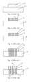
- FIG. 1 a - 1 eA brief discussion of manufacturing steps commonly used in the prior art will now be given with reference to FIG. 1 a - 1 e , labeled “prior art”. This discussion is given for the purpose of giving some context to the further discussion below, but without limitation to the discussion that will follow.
- FIG. 1 a - FIG. 1 eThe material chosen and microfabrication method for the vertical comb drive actuator is shown in FIG. 1 a - FIG. 1 e .
- a Silicon-Silicon Oxide-Silicon material(shown in FIG. 1 a ) is used to make micromirror, electrical interconnection wires and vertical comb drive actuators.
- a dielectric material 2such as silicon oxide is used to electrically isolate the conductive silicon layer 1 and conductive silicon layer 3 (shown in FIG. 1 a ).
- First, lithography and silicon DRIE (Deep Reactive-Ion Etching)are used to etch the silicon layer 1 (shown in FIG. 1 b ).
- the silicon oxide layer 2is an excellent etching stop material to silicon DRIE to prevent the further silicon etching into silicon layer 3 .
- the thickness of the silicon oxide layeris typically over a couple of microns in order to withstand an electrical voltage applied between silicon layer 1 and 3 that may be over a couple of hundred volts.
- the air gap between finger 4 and 5is made as small as possible in order to have higher energy density (shown FIG. 1 b ), and the height of the finger 4 and 5 is made as tall as possible to have a larger angle of rotation for the mirror. All these requirements result in the high aspect ratio geometry between fingers 4 and 5 . Etching the silicon oxide 6 between fingers 4 and 5 becomes extremely difficult or impossible for a silicon oxide thickness of over a couple of microns (shown in FIG. 1 c ).
- a micromirror and by extension a micromirror arraymay be made from a single layer of electrical conductive single crystal silicon 10 with trenches 13 refilled with dielectric materials such as silicon oxide, and sometimes also with cavity filling material such as polysilicon to make both the micromirror 21 and micromirror array and electrical vertical comb drive actuators 15 , (shown in FIG. 2 a ).
- the trenches 13 refilled with dielectric materialsare used to electrically isolate the three electrical actuation electrodes 16 a , 19 a and 20 a ) for each micromirror with 2 dimensional rotations.
- the trenchesalso mechanically join these electrodes together.
- a self-alignment microfabricationis preferably used to make electrostatic vertical comb drive actuators on the single layer of electrical conductive single crystal silicon 10 , which allows smaller air gaps between comb fingers and taller finger height for larger mirror rotation angles at lower actuation voltages to be more easily achieved.
- This designpreferably uses a carrier wafer 11 (shown in FIG. 2 a and FIG. 2 b ) for the routing of electrical interconnections.
- the carrier wafercould be either partial wafer thickness or full wafer thickness TSV (Through Silicon Via) type of wafers, or glass (such as Pyrex) wafer with multiple thin film metal layers used for the dense electrical interconnections.
- TSV type of carrier wafer 11is shown in FIG. 2 a and FIG. 2 b .
- the carrier wafer 11has electrical conductive silicon via or posts 17 b , 18 b , 19 b and 20 b (shown in FIG. 2 a and FIG. 2 b ). Each silicon via or post is surrounded by a trench 22 refilled with dielectric material such as silicon oxide, sometimes also with cavity filling material such as polysilicon to provide the electrical isolation.
- the carrier wafer 11is bonded with the single layer of conductive single crystal silicon 10 .
- the electrical interconnectionsare established vertically to the bottom metal bonding pads 17 c , 18 c , 19 c and 20 c through the electrode 17 a , 18 a , 19 a and 20 a and the silicon via or post 17 b , 18 b , 19 b and 20 b .
- the high density of electrical interconnectionscan be easily established for the very large micromirror arrays with a higher filling factor.
- FIGS. 3 a - 3 mAn example of the major microfabrication steps that may be used arrive at the depicted embodiment is shown in FIGS. 3 a - 3 m , and described below.
- a self-alignment silicon etching microfabrication processmay be used to make the electrostatic vertical comb drive actuators on the single layer of electrical conductive single crystal silicon 30 (shown in FIG. 3 a ).
- FIG. 3 ashows the starting material for both micromirror and vertical comb drive actuators.
- a layer of electrical conductive single crystal device silicon 30has silicon etched trench 31 refilled with dielectric materials such as silicon oxide, and sometimes also with cavity filling material such as polysilicon.
- Silicon 30 , Buried Oxide (BOX) layer 32 and handle silicon wafer 33form a typical SOI (Silicon On Insulator) wafer.
- the starting SOI wafer with trenching and refilled device silicon layerwhich may also be referred to as a silicon layer with isolation trenches, can be either made in house or custom made by silicon wafer vendors. Silicon DRIE may subsequently performed to etch about half thickness of the silicon layer 30 (shown in FIG. 3 b ) for the purposes of the mirror weight reduction and/or flexible hinge height reduction etc.
- FIG. 3 cshows the starting material for making the carrier wafer.
- a conductive single crystal silicon wafer 35has silicon etched trenches 36 refilled with dielectric materials such as silicon oxide, and sometimes also with cavity filling material such as polysilicon.
- the trenchesare typically not all the way through the full thickness of wafer 35 , the trenching 36 depth is determined by the specific design requirements of the micromirror and micromirror array, for example, the trenching depth could be 2 ⁇ 3 of the wafer thickness.
- this starting materialcan be either made in house or custom made by silicon wafer vendors.
- a silicon DRIEis subsequently performed from the wafer top surface to reach the trenches 36 (shown in FIG. 3 d ) so that silicon via or post 37 and 38 are electrically isolated.
- FIG. 3 eshows the wafer bonding of wafer 30 and carrier wafer 35 .
- FIG. 3 fshows the etching away of the handle wafer 33 .
- the thin film metal bonding pads 39can be made on the back side of wafer 35 . These bonding pads can be used for solder balls or wired bonding.
- Partial silicon oxide etchingis performed on the silicon oxide layer 32 in the place 40 where the lower comb finger will be located. Typically half of the silicon oxide layer 32 thickness is etched away. And then lithography step and silicon oxide etching are conducted to prepare the silicon oxide DRIE etching mask for upper and lower fingers as well as other features such as mirror structures, hinges and electrodes etc.
- the oxide mask 42 for upper comb fingeris thicker than the oxide mask 41 for lower comb finger (shown in FIG. 3 h ).
- the first silicon DRIEetches through the silicon 30 to form the upper comb fingers and partially finished lower comb fingers (shown in FIG. 3 i ).
- An oxide RIEReactive Ion Etching
- the second silicon DRIEetches the half thickness of the silicon layer 30 to form the lower comb finger 44 (shown in FIG. 3 k ).
- the upper comb finger 45 and lower comb finger 44are finished after removal of the oxide layer 32 using oxide RIE (shown in FIG. 3 l ).
- the optical reflective thin film 49such as Au thin film and thin film electrode metal 50 can be placed on the top of mirror structure 47 and electrode 48 respectively using metal PVD (Physical Vapor Deposition) such as sputtering with a shadow mask (shown in FIG. 3 m ).
- the mirror metal 49 and bonding pad metal 50can be also deposited, patterned and protected before the first DRIE (shown in FIG. 3 j ).
- FIG. 4The detailed view of the micromirror with vertical comb drive actuators is shown in FIG. 4 .
- the trenches 13refilled with dielectric materials such as silicon oxide, and sometimes also with cavity filling material such as polysilicon electrically isolate the mirror supporting frame 60 from the silicon connection regions 70 .
- the silicon connection regions 70form the electrical paths and mechanical supporting structures for the fixed vertical comb drive fingers 74 and 75 .
- the comb fingers 74 and 75 on the silicon connection regions 70are electrically connected to the fixed electrode 19 a and 20 a respectively through silicon connection regions 70 and silicon hinge 62 .
- the mirror 21 with its comb fingers and optical reflective coating 14 , the mirror supporting frame 60 with its comb fingers and electrodes 16 aare mechanically and electrically connected through the silicon hinges 61 and 63 (shown in FIG. 4 ).
- the electrodes 16 a , 17 a , 18 a , 19 a and 20 aare mechanically fixed to the vias or posts of the carrier wafer.
- Both the mirror 21 and mirror supporting frame 60can be actuated to have the first dimensional rotation along X axis/the hinges 62 and 63
- mirror 21can also be actuated to have the second dimensional rotation along Y axis/the hinge 61 (shown in FIG. 4 ).
- Hinges 61 , 62 and 63are part of what may be referred to as a pivoting structure, and are connected between anchors and the micromirror structure.
- the anchorsmay be fixed to a substrate, or may be the moving portion of the micromirror, where the particular hinge pivots relative to that moving portion.
- the moving portionmay be considered a stationary structure for the purposes of pivoting the mirror about a second pivot axis.
- micromirror structureis intended to include components such as mirror 21 and mirror supporting frame 60 in this example. Depending on the particular micromirror design, the term may also be used to include other components that will be recognized by those skilled in the art, or may be used to simply refer to mirror 21 .
- it is preferable to design the pivot axes that are perpendicularas this generally simplifies operation of the micromirror.
- it is also possible to design the pivot axes at angles that are not perpendicularwith the understanding that, to achieve pivoting in two dimensions, the pivot axes must be non-parallel.
- the electrostatic force resulting in between the fixed upper comb fingers on the fixed electrodes 18 a and lower comb fingers on the mirror supporting frame 60will actuate the mirror supporting frame 60 with mirror 21 clockwise about the axis X (shown in FIG. 4 ).
- the electrostatic force resulting in between the fixed upper comb fingers on the fixed electrodes 17 a and lower comb fingers on the mirror supporting frame 60will actuate the mirror supporting frame 60 with mirror 21 counterclockwise about the axis X (shown in FIG. 4 ).
- the electrostatic force resulting in between the fixed upper comb fingers on the silicon regions 70 and lower comb fingers on the extension arms 80 from the mirror 21will actuate the mirror 21 clockwise about the Y axis (shown in FIG. 4 ).
- a comb finger with different shapessuch as stepped shape 91 and taper shape 92 (shown in FIG. 5 a ) may be used.
- FIG. 5 bshows another method to strengthen the mechanical strength of comb fingers.
- the fixed anchors 104are attached to the hinges 105 of the structure 106 such as, rotation axis shaft, mirror, etc.
- the vertical comb drive actuatorincludes fixed lower comb fingers 107 .
- the effective strategywould be to increase the finger density, i.e., to reduce the comb finger pitches between adjacent two moveable fingers and/or adjacent two moveable fingers, and increase the interactive length between fixed and moveable fingers.
- the thin and long moveable comb fingers 103are used to increase the actuation power of the actuators.
- the thin and long moveable comb fingershave weak mechanical strength which will increase the likelihood of device malfunctions such as electrical shorting between fixed fingers and moveable fingers due to undesired bend of movable fingers.
- structural beams 108 and 109may be provided to prevent the moveable fingers from unintentionally bending.
- the position of the strengthening beammay vary, but is generally spaced from the mirror structure, and connects the movable fingers 103 together along at least a portion of the top surface of the movable fingers 103 such that the movable fingers 103 extend downward from the structural element 108 and 109 . This is required to allow the comb drive to operate, as the fixed fingers 107 traverse the structural elements 108 and 109 .
- top surfaceis defined relative to the fixed fingers 107 , which are “below” the movable fingers 103 .
- itcould be provided at the tip of the movable fingers, such as beam 108 , or may be spaced a certain distance from the fingertip, such as the beam 109 .
- the material of the strengthening beamis preferably single crystal silicon shown in FIG. 5 b .
- the height and width of the beammay be relatively small.
- the silicon beam structure 108 and 109may be fabricated using the process flow shown in FIG. 3 a - 3 m , but other beam materials and similar structure to achieve the same functions could be easily made to the experts in the field.
- FIG. 5 cshows design variations of the strengthening beams of comb drive fingers for the mirror structure.
- the orientation of moveable comb finger 103 a and fixed comb finger 107 ais parallel to the rotation hinge 105 .
- the strengthening beams 108 a , 109 a and 109 bare used to strength the movable comb fingers 103 a.
- the depicted examplesinclude a taper shape 95 , a serpentine shape 96 , a V shape 97 , a multiple stepped parallel arm shape 101 , and a connected multiple stepped parallel arm shape 98 .
- Other designsmay also be used, as will be recognized by those skilled in the art. These shapes may be used to increase the design and micro fabrication flexibilities.
- the hingesare used to connect the movable structure 99 , such as mirror supporting frame or mirror, to the fixed or relative fixed part 100 such as fixed electrodes or the mirror supporting frame.
- fixed part 100may be part of a movable portion itself, it will be understood that it may be considered fixed relative to the movable structure 99 .
- a preferred hinge designis indicated by reference numeral 101 .
- This hingehas a first side 101 a , a second side 101 b , a first end 102 a connected to a movable structure, such as a mirror 99 as shown, and a second end 102 b connected to a fixed structure, such as an anchor 100 as shown.
- Each of the first side 101 a and the second side 101 bis made up of a beam with a series of discrete, alternating angles between the first end 102 a and the second end 102 b .
- hinge bodyThe alternating angles causing the hinge body to become progressively narrower moving from the first end to the second end. As can be seen, the first and second sides defining a single aperture within the hinge body. This may be contrasted with hinge 98 , which defines multiple apertures in its shape.
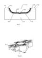
- the back side of the mirror 111may be partially etched away to reduce the mechanical mass in order to increase its mechanical response speed and anti-shock ability by reducing the inertia force in the vibration and shock environments.
- Examples of circular, square and hexagon etching geometriesare shown in FIG. 7 . Other geometries known to those skilled in the art may also be used.
- the depicted glass wafer 110has via holes filled with metal 112 used for the electrical interconnections.
- the glass wafer 110can be any glass material, including Pyrex which allows anodic bonding.
- the top surface of the metal 112is preferably slightly higher than the glass wafer top surface 113 for easy electrical connection with the bottom surfaces of bonded conductive silicon electrodes 16 a , 17 a , 18 a , 19 a and 20 a shown in FIGS. 2 a , 2 b and 4 .
- a metal film 114may be included for wire bonding or for solder balls.
- a cavity 116 on the glass wafer 110is etched to provide spaces for the rotations of the mirrors and mirror supporting frames.
- a thin metal filmis deposited and patterned on the cavity surface to provide an electrical ground surface to shield the electrical charges from the glass wafer 110 .
- the glass based carrier wafercan use multiple thin metal layers for the electrical interconnections.
- the glass wafer 110is etched with a shallow cavity 124 and a deep cavity 116 to accommodate the metal electrical interconnection wires 120 and 121 .
- the top surfaces of the metal wires 120 and 121are preferably slightly higher than the glass surface 113 for easy electrical connection with the bottom surfaces of bonded conductive silicon electrodes 16 a , 17 a , 18 a , 19 a and 20 a , shown in FIGS. 2 a , 2 b and 4 .
- a thin layer of dielectric materialsuch as silicon oxide or silicon nitride 122 is deposited and patterned on the metal 120 and 121 .
- a thin metal film 123is deposited and patterned on the dielectric material 122 to provide an electrical ground surface to shield the electrical charges from dielectric material 122 , and also the electrical interferences from the wires 120 and 121 .
- Extra interconnection metal layers and dielectric material layerscan be added as described to increase the capacity of the electrical interconnections.
- the mechanical support and electrical connectors, via/posts, which are used to connect to a micromirror, such as a micromirror, shown in FIGS. 2 a , 2 b and 4 ,may also be made with the mirror and actuator wafer 10 , as shown in FIG. 10 .
- the fabrication of the posts 130will be obvious to the expert in the field.
- the carrier wafermay be flat silicon or glass based TSV carrier wafer.
- the flat silicon based TSV carrier waferis shown in FIG. 11 , where a trench 36 is refilled with dielectric materials on silicon wafer 35 , which may be used to electrically isolate bonding pad metal 39 on the wafer.
- the flat glass carrier wafer with TSV or with multiple thin films metal layersis shown in FIGS. 12 and 13 respectively.
- the top surfaces of the metal vias 112are preferably slightly higher than the glass surface 113 for easy electrical connection with the bottom surfaces of bonded conductive silicon electrodes.
- the top surfaces of the metal wires 120 and 121are shown to be slightly higher than the glass surface 113 for easy electrical connection with the bottom surfaces of bonded conductive silicon electrodes.
- a thin layer of dielectric materialsuch as silicon oxide or silicon nitride 122 is deposited and patterned on the metal 120 and 121 .
- a thin metal film 123is then deposited and patterned on the dielectric material 122 to provide an electrical ground surface to shield the electrical charges from dielectric material 122 , and also the electrical interferences from the wires 120 and 121 .
- Extra interconnection metal layers and dielectric material layerscan be added as described to increase the capacity of the electrical interconnections.
- FIG. 14 through 18are included to show examples of embodiments using some of the options described above.
- FIGS. 14 and 15show a detailed design of a micromirror 143 with detailed view of its electrodes 144 a , 144 b and 144 c , hinges 146 a and 146 b , mirror 148 , mirror frame 150 , comb drives 152 a and 152 b , trenching and refilling areas 154 etc. Trenching and refilling areas 154 may also be referred to as “isolation trenches”.
- the hinges 146 bconnect the mirror 148 to the mirror frame 150 that circumscribes the mirror 148 , and the hinges 146 b permit rotation of the mirror 148 relative to the frame 150 .
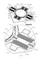
- FIGS. 16 a and 16 bshow a micromirror array 156 using the partial wafer thickness TSV type carrier wafer 158 .
- the electrical connections 159will be channeled out to the external control system from the metal bonding pads on the backside of the chip. It can be easily seen that the mirror array can be easily scaled up without any limitation issue of electrical interconnections.
- FIGS. 17 and 18show a micromirror array 155 using a glass carrier wafer 157 .
- the electrical connectionswill be routed out to the bonding pad 140 around the chip edge in FIG. 17 .
- FIG. 18shows a micromirror array 155 using a micromirror, vertical comb drive actuators with silicon electrical and mechanical posts. The electrical connections will be routed out to the bonding pad 142 around the chip edge.
- a relatively simple lithography alignment process techniquemay be used to make the vertical comb drive actuators and other mirror structures from two layers of electrical conductive single crystal silicon.
- the processmay be used in many various MEMS structures that involve interaction between multiple layers.
- the basic steps of this process to make the MEMS structureinclude etching a first layer with a reference mark and the first portion of the MEMS structure, attaching a second layer to the first layer, the second layer overlying the first layer, etching an opening through the second device layer to reveal the reference mark, and etching the second portion of the MEMS structure in the second layer based on the position of the reference mark.
- FIG. 19shows a mirror structure and vertical comb drive actuators fabricated by the lithography alignment process.
- the fixed comb fingers set 171 , 172 , 175 and 176 , electrode 160 and 161are fabricated from the lower layer of electrical conductive single crystal silicon
- mirror 168 , gimbal structure 169 , flexible hinges 165 and 166 , moveable comb finger supporting arms 170 and 178 , moveable comb fingers 173 , 174 , 177 and 179 , electrode 162 , 163 and 164are made from the upper layer of electrical conductive single crystal silicon.
- An optical reflective thin film 167such as Au thin film may be deposited and patterned on the top surface of the silicon mirror 168 .
- the mirror 168 , gimbal structure 169 , flexible hinges 165 and 166 , moveable comb finger supporting arms 170 and 178 , moveable comb fingers 173 , 174 , 177 and 179will be at the zero electrical potential.
- the structural designs for the hinge shape design and vertical comb drive actuatorsplay an important role.
- the hinge designsmay be selected from the hinge shapes shown in FIG. 6 , or others known to those skilled in the art.
- the orientation of the movable and fixed comb drive fingers of vertical comb drive actuators for Y axis tiltingis preferably parallel to the Y axis as shown in FIG. 19 and FIG. 23 g and FIG. 23 h , or other shapes shown in FIG. 23 a - 23 f .
- the shapes of movable and fixed comb drive fingersmay be one straight beam shape, arc shape, or multiple straight beam segments shapes.
- the comb drive fingersare preferably designed such that both the fixed and movable fingers extend in a direction having a component that is parallel to the axis of rotation.
- the fingersalso have another component that is perpendicular to the axis of oration, which allows the fingers to follow or estimate the radius of curvature as it extends outward from the hinge.
- the fingerswill extend in a direction that includes an X component, and may be entirely parallel to the axis of rotation.
- the fingerswill also have a Y component, which matches or approximates the radius of curvature as defined by the distance of the fingers from the hinge, either by segments or by a curved finger.
- the movable fingersare preferably offset relative to the fixed fingers to account for this to avoid any contact between the fingers. Generally speaking, this will require the movable fingers to be moved back from the fixed fingers relative to the axis. In other words, considering a single movable finger positioned between two fixed fingers, where the first fixed finger is closer to the hinge, the movable finger will be closer to the second fixed finger.
- each design in FIG. 23 a through 23 hhas the movable fingers 211 positioned within a frame, while the fixed fingers 212 are similar to posts extending upward from the substrate. This is done to increase the stability of the movable fingers 211 .
- Other designsmay also be used, such as movable fingers that extend outward from a central beam to engage fixed fingers.
- FIG. 20 a - 20 gThe major process steps in the lithography alignment process described herein are illustrated in FIG. 20 a - 20 g , with respect to an example of the fabrication of a vertical comb drive actuator. It will be understood that this example only shows the general steps used to make vertical comb drives and mirror structures, and that process variations may be used in other MEMS structures that require more than one layer, such as a microphone structure, gyroscope sensor structure, accelerometer sensor structure, etc. While FIG. 20 a - 20 g shows an example of how the process may be used to fabricate a vertical comb drive actuator, similar steps can be used to make the mirror structure, hinges structure, other actuators, etc. Some extra process steps may also be added to make other mirror structures such as the reflective thin film metal on the mirror surface, as will be recognized by those skilled in the art.
- a regular SOI (Silicon On Insulator) waferis shown with device layer 180 , dielectric, such as BOX (Buried Oxide), layer 181 and a handle layer 182 , such as a silicon handle layer.
- dielectricsuch as BOX (Buried Oxide)
- handle layer 182such as a silicon handle layer.
- a DRIE processis then used to etch the device layer 180 .
- the lower comb drive finger 184is fabricated along with the alignment reference mark 183 .
- An oxide RIE processis used in FIG. 20 c to etch away the oxide 185 between the lower comb drive fingers formed in FIG. 20 b .
- the wafer bondingis shown in FIG.
- FIG. 20 dbetween etched SOI wafer and another SOI wafer with device layer 189 , BOX layer 188 and handle wafer 187 . All the silicon layers of both SOI wafers are electrical conductive.
- a silicon etching processsuch as DRIE is used to open a window 190 on the device layer 189 as shown in FIG. 20 f , and lithography alignment tools such as contact lithography mask aligner and/or stepper lithography mask aligner are able to align the upper comb drive fingers 191 to the lower comb drive finger 184 with the help of the reference mark 183 .
- a silicon DRIEis used to fabricate the upper comb drive finger 191 .
- a single two dimensional tilting mirrorsuch as the example shown in FIG. 19 , can be fabricated using the process shown in FIG. 20 a - 20 g . If the full or partial wafer thickness TSV silicon wafer is used during the device fabrication, then the mirror shown in FIG. 21 a may be made with vertical electrical interconnections and can be used to form a very large mirror array with high fill factor.
- a partial wafer thickness TSV silicon wafer 196is used to replace the regular SOI wafer with device layer 180 , BOX layer 181 and handle silicon layer 182 .
- the DRIEwill be used to etch the silicon to reach the top of the trenching and refilled rings.
- the electrical insulation trenching and refilled rings 200are exposed and shown in FIG. 21 a .
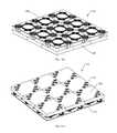
- FIG. 21 bshows the part of very larger mirror array 201 with high fill factor.
- FIG. 22 ashows a one dimensional tiling mirror 203 fabricated using the partial wafer thickness TSV silicon wafer and the simple lithography alignment process.
- the vertical comb drive actuator 202will tilt the mirror 203 about the hinge 204 .
- the varieties of high fill factor micromirror array 205can be formed using the mirror 203 shown in FIG. 22 a .
- a one dimensional mirror array 205 a with high fill factoris shown in FIG. 22 b .
- a two dimensional mirror array 205 b with high fill factoris shown in FIG. 22 c.
- FIG. 23 a - 23 hshows some examples vertical comb drive actuators.
- FIG. 23 ashows a fixed comb drive fingers 208 , 212 and moveable vertical comb drive fingers 206 , 211 .
- the actuatorwill tilt the structure 213 about the rotation hinge 210 .
- the hinge 210is anchored by 217 .
- the ideal shape of moveable comb drive finger 211is the arc shape with the radius of R from the axis center point 209 .
- the other fingers 206 , 208 and 212will be designed in the same manner. Therefore the radius of finger 206 is smaller that radius of finger 211 , also the radius of finger 208 is smaller that radius of finger 212 . Due to the rotation of the structure 213 , the moveable finger 211 will rotate close to fixed comb finger 208 , while it will rotate away from the finger 212 . For this reason, the initial position of finger 211 is not designed in the middle position between fixed finger 208 and 212 . Instead, the finger 211 is designed a bit close to the finger 211 initially to increase the rotation stability and tilting range of the acuators.
- FIG. 23 bshows a design variation of vertical comb drive shown in FIG. 23 a .
- the moveable comb driveis cut to have opening 214 to allow movement of the structure 216 without mechanical and electrical interferences between fixed and moveable fingers.
- the structure 216is used to connect the fixed comb drive fingers to the mechanical anchor and electrical actuation electrode.
- FIGS. 23 c and 23 dshow fingers with multiple straight beam segments are designed to resemble the arc shape to the rotational axis point 209 .
- the straight beam segmentshave very small angles (such as less than 3 degrees) to the rotational axis.
- FIGS. 23 e and 23 fshow fingers with the one straight beam segment to resemble the arc with larger radius R.
- FIGS. 23 g and 23 hshow straight beam finger which is parallel to the rotation axis 209 , when the radius R is sufficient large.
- FIG. 24 ashows a one dimensional tilting mirror fabricated using the partial wafer thickness TSV silicon wafer and the lithography alignment process described previously.
- the vertical comb drive actuators 220tilt the mirror about the hinges 222 clockwise and counterclockwise.
- a variety of high fill factor micromirror arraymay be formed using the mirrors structure shown in FIG. 24 a .
- a two dimensional mirror array 223 formed with high fill factoris shown in FIG. 24 b.
- FIG. 25 ashows a one dimensional tilting mirror fabricated using the partial wafer thickness TSV silicon wafer and the lithography alignment process described previously.
- the vertical comb drive actuators 230tilt the mirrors 231 about the hinges 232 clockwise and counterclockwise.
- the varieties of high fill factor micromirror arraycan be formed using the mirror structure shown in FIG. 25 a .
- a thin silicon wall 234surrounds the mirror structure and vertical comb drive actuators. If this wall is connected to the electrical ground, then it will provide two functions. One is to provide an electrical shield to avoid the electrical interference between actuators of adjacent mirrors in the array structure. The other is to provide a mechanical barrier for the squeezed air flow resulting from the actuation of the mirror.
- a two dimensional mirror array 235 formed with high fill factoris shown in FIG. 25 b .
- the thin silicon wall 234can be removed if required, for example, by limited space between adjacent two mirror structures. If needed, however, the thin silicon wall structure may be implemented in some or all of the mirrors and mirror array.
- the lithography alignment process described previouslymay also be used to make the two dimensional tilting mirrors shown in FIG. 26 a - 26 c .
- the depicted tilting mirrorsinclude a mirror 244 , movable fingers of the vertical comb drive actuator 240 for tilting about the X axis, X-axis hinges 239 , weight balance part 249 , supporting arm structures 248 , movable fingers of the vertical comb drive actuators 243 for tilting about the Y axis, Y-axis hinges 238 and supporting arms 247 for movable fingers suspended/anchored by two electrode structures 236 .
- the mirror 244movable fingers of the vertical comb drive actuator 240 for tilting about the X axis, X-axis hinges 239 , weight balance part 249 , supporting arm structures 248 , movable fingers of the vertical comb drive actuators 243 for tilting about the Y axis, Y axis hinges 238 and supporting arms 247 for movable fingers are at zero electrical potential.
- FIG. 26 bshows a design variation of the mirror structure shown in FIG. 26 a .
- the actuator 241will rotate the mirror 244 and X axis hinges 239 about the X axis/hinge 239 counterclockwise.
- FIG. 26 cshows another design variation of the mirror structure shown in FIG. 26 a .
- the actuators 246 and 245will rotate the mirror 244 and X axis hinges 239 about the X axis/hinge 239 clockwise and counterclockwise.
- the mirror array 272 a shown in FIG. 27 acan be formed by mirror structure shown in FIGS. 26 a and 26 b
- another mirror array 272 b shown in FIG. 27 bcan be formed by mirror structure shown in FIG. 26 c .
- These mirror arrayswill have high fill factor.
- the thin silicon wallcan be added to the mirror structures shown in FIGS. 26 a and 26 c and mirror array structures shown in FIGS. 27 a and 27 b .
- FIG. 28 ashows a two dimensional tilting mirror structure 282 with thin silicon wall 250
- FIG. 28 bshows the mirror array structure 284 formed by the mirror structure 282 shown in FIG. 28 a.
- the weight balance part 249is used to balance the weight of mirror 244 to achieve good mirror stability. In the vibration and shocking environments, the inertial force from the mirror weight will result in undesirable mirror tiling about the X axis/hinges 239 .
- the thicker and higher density metal filmcan be deposited on the top surface of weight balance part 249 with the larger size and thicker silicon structure in order to have the same inertial force torque to the X axis/hinges 239 as the mirror 244 .
- weight balance parts 261 , 262 and 263may be used in the mirror structure.
- the mirrors 260will have clockwise and counterclockwise rotation about the Y axis
- the mirrors 260will have clockwise and counterclockwise rotation about the X axis.
- FIG. 29 adepicts an example of a mirror structure fabricated using partial wafer thickness TSV silicon wafer 266 and the lithography alignment process described above.
- the mirror structure shown in FIG. 29 bmay be fabricated using partial wafer thickness TSV silicon wafer and the simple lithography alignment process, or can be fabricated using regular SOI wafer and the simple lithography alignment process.
- the mirror structure with thin silicon wall 267 shown in FIG. 29 cis fabricated using partial wafer thickness TSV silicon wafer 268 and the simple lithography alignment process.
- actuators 251 , 253 and 255may be removed from the mirror structures shown in FIG. 29 a , FIG. 29 b and FIG. 29 c respectively.
- the mirror structures shown in FIG. 29 a - 29 bmay be used to form the mirror array structures shown in FIG. 22 b , FIG. 22 c , FIG. 24 b , FIG. 25 b , FIG. 27 a , FIG. 27 b and FIG. 28 b.
- the trenching and refilled region 288electrically isolate and mechanically connect the electrode 283 , hinge 284 and 285 , connection part 312 , pad 286 , and fixed comb drive fingers 287 with electrode pad 280 , hinge 281 , moveable comb drive fingers 292 and 293 , supporting arms 311 for the moveable comb drive fingers, supporting arm 300 , hinge 296 and mirror 301 .
- the hinge 281 , moveable comb drive fingers 292 and 293 , supporting arms 311 for the moveable comb drive fingers, supporting arm 300 , hinge 296 and mirror 301are at zero electrical potential.
- an electrical potentialis applied to the fixed comb drive fingers 290 and 291 , the resulting electrostatic forces will rotate the hinge 281 and 284 , moveable comb drive fingers 292 and 293 , supporting arms 311 for the moveable comb drive fingers, supporting arm 300 , hinge 296 and mirror 301 clockwise and counterclockwise about the Y axis/hinge 281 and 284 .
- FIG. 30 bshows a mirror structure with a vertical comb drive actuator 310 and 311 to tilt the mirror 301 clockwise and counterclockwise about the X axis/hinge 296 .
- FIGS. 30 a and 30 bThe design variations can be implemented to the mirror structure shown in FIGS. 30 a and 30 b .
- a balance weight partcan be added between hinge 296 and vertical comb drive actuator 311 , and vertical comb drive actuator 310 can be moved to the end edge 312 of the mirror 310 .
- the mirror structures shown in FIG. 30 a - 30 bmay be used to form the mirror array structures shown in FIG. 22 b , FIG. 22 c , FIG. 24 b , FIG. 25 b , FIG. 27 a , FIG. 27 b and FIG. 28 b.
Landscapes
- Physics & Mathematics (AREA)
- General Physics & Mathematics (AREA)
- Optics & Photonics (AREA)
- Mechanical Light Control Or Optical Switches (AREA)
- Micromachines (AREA)
Abstract
Description
Claims (30)
Priority Applications (5)
| Application Number | Priority Date | Filing Date | Title |
|---|---|---|---|
| US13/267,045US9036231B2 (en) | 2010-10-20 | 2011-10-06 | Micro-electro-mechanical systems micromirrors and micromirror arrays |
| US14/702,874US10551613B2 (en) | 2010-10-20 | 2015-05-04 | Micro-electro-mechanical systems micromirrors and micromirror arrays |
| US16/742,296US11567312B2 (en) | 2010-10-20 | 2020-01-14 | Micro-electro-mechanical systems micromirrors and micromirror arrays |
| US18/145,302US11927741B2 (en) | 2010-10-20 | 2022-12-22 | Micro-electro-mechanical systems micromirrors and micromirror arrays |
| US18/537,100US20240111148A1 (en) | 2010-10-20 | 2023-12-12 | Micro-electro-mechanical systems micromirrors and micromirror arrays |
Applications Claiming Priority (2)
| Application Number | Priority Date | Filing Date | Title |
|---|---|---|---|
| US45534810P | 2010-10-20 | 2010-10-20 | |
| US13/267,045US9036231B2 (en) | 2010-10-20 | 2011-10-06 | Micro-electro-mechanical systems micromirrors and micromirror arrays |
Related Child Applications (1)
| Application Number | Title | Priority Date | Filing Date |
|---|---|---|---|
| US14/702,874DivisionUS10551613B2 (en) | 2010-10-20 | 2015-05-04 | Micro-electro-mechanical systems micromirrors and micromirror arrays |
Publications (2)
| Publication Number | Publication Date |
|---|---|
| US20120099176A1 US20120099176A1 (en) | 2012-04-26 |
| US9036231B2true US9036231B2 (en) | 2015-05-19 |
Family
ID=45972821
Family Applications (1)
| Application Number | Title | Priority Date | Filing Date |
|---|---|---|---|
| US13/267,045Active2032-01-05US9036231B2 (en) | 2010-10-20 | 2011-10-06 | Micro-electro-mechanical systems micromirrors and micromirror arrays |
Country Status (1)
| Country | Link |
|---|---|
| US (1) | US9036231B2 (en) |
Cited By (7)
| Publication number | Priority date | Publication date | Assignee | Title |
|---|---|---|---|---|
| CN109581653A (en)* | 2019-01-25 | 2019-04-05 | 山东大学 | A kind of MEMS actuator and its working method based on prominent comb teeth |
| US10429590B1 (en)* | 2018-05-21 | 2019-10-01 | Dicon Fiberoptics, Inc. | Damping mechanism for micro-electro-mechanical systems (MEMS) structures, including tilting mirror devices used in optical components |
| US10509198B1 (en) | 2018-12-07 | 2019-12-17 | Didi Research America, Llc | Lever system for driving mirrors of a lidar transmitter |
| US11061201B2 (en) | 2018-12-07 | 2021-07-13 | Beijing Voyager Technology Co., Ltd. | Non-linear springs to unify the dynamic motion of individual elements in a micro-mirror array |
| US11085995B2 (en) | 2018-12-07 | 2021-08-10 | Beijing Voyager Technology Co., Ltd. | Non-linear springs to unify the dynamic motion of individual elements in a micro-mirror array |
| US20230143512A1 (en)* | 2020-04-28 | 2023-05-11 | Zkw Group Gmbh | Illumination Apparatus for a Motor Vehicle Headlamp |
| US20240272004A1 (en)* | 2023-02-10 | 2024-08-15 | Stmicroelectronics International N.V. | Process flow for thin contactless thermal sensors |
Families Citing this family (45)
| Publication number | Priority date | Publication date | Assignee | Title |
|---|---|---|---|---|
| US9269536B2 (en)* | 2012-04-17 | 2016-02-23 | Varian Semiconductor Equipment Associates, Inc. | Double ended electrode manipulator |
| TWI493743B (en)* | 2012-11-06 | 2015-07-21 | Asia Pacific Microsystems Inc | Self-aligned vertical comb - shaped sensor and its manufacturing method |
| US20140126034A1 (en)* | 2012-11-07 | 2014-05-08 | Canon Kabushiki Kaisha | Variable shape mirror and method of manufacturing the same |
| US9335544B2 (en)* | 2013-03-15 | 2016-05-10 | Rit Wireless Ltd. | Electrostatically steerable actuator |
| DE102013206377B4 (en)* | 2013-04-11 | 2021-07-29 | Robert Bosch Gmbh | Micromechanical structure and corresponding manufacturing process |
| US20160139340A1 (en)* | 2013-06-27 | 2016-05-19 | Oplink Communications, Inc. | Mems fiber optical switch |
| US9575259B2 (en) | 2013-07-02 | 2017-02-21 | Finisar Corporation | N×N optical switch |
| JP6467347B2 (en)* | 2013-11-07 | 2019-02-13 | 住友精密工業株式会社 | Semiconductor device |
| DE102014211546B4 (en) | 2014-06-17 | 2022-08-25 | Robert Bosch Gmbh | MICROSMIRROR ARRANGEMENT |
| JP6696777B2 (en)* | 2016-01-21 | 2020-05-20 | 浜松ホトニクス株式会社 | Actuator device |
| JP6691784B2 (en)* | 2016-01-21 | 2020-05-13 | 浜松ホトニクス株式会社 | Actuator device |
| JP6814892B2 (en)* | 2017-01-27 | 2021-01-20 | フラウンホーファーゲゼルシャフト ツール フォルデルング デル アンゲヴァンテン フォルシユング エー.フアー. | Methods for Providing MMS, MMS Arrays, MEMS Actuators and MMS |
| US11513339B2 (en) | 2017-03-14 | 2022-11-29 | Hamamatsu Photonics K.K. | Optical module |
| JP6778134B2 (en) | 2017-03-14 | 2020-10-28 | 浜松ホトニクス株式会社 | Optical module and its mounting method |
| CN110418994B (en)* | 2017-03-14 | 2022-04-19 | 浜松光子学株式会社 | Optical module |
| DE112018001385T5 (en) | 2017-03-14 | 2019-11-28 | Hamamatsu Photonics K.K. | light module |
| CN107264416B (en)* | 2017-06-29 | 2019-11-26 | 京东方科技集团股份有限公司 | A kind of rearview mirror and its driving method |
| CN110799889B (en)* | 2017-07-06 | 2022-06-03 | 浜松光子学株式会社 | Optical device |
| US11635613B2 (en) | 2017-07-06 | 2023-04-25 | Hamamatsu Photonics K.K. | Optical device |
| CN115598830A (en) | 2017-07-06 | 2023-01-13 | 浜松光子学株式会社(Jp) | Optical device |
| JP6514804B1 (en) | 2017-07-06 | 2019-05-15 | 浜松ホトニクス株式会社 | Optical device |
| JP7112876B2 (en) | 2017-07-06 | 2022-08-04 | 浜松ホトニクス株式会社 | optical device |
| TWI833699B (en) | 2017-07-06 | 2024-03-01 | 日商濱松赫德尼古斯股份有限公司 | Optical device |
| US11187872B2 (en) | 2017-07-06 | 2021-11-30 | Hamamatsu Photonics K.K. | Optical device |
| EP3650916A4 (en) | 2017-07-06 | 2021-03-10 | Hamamatsu Photonics K.K. | OPTICAL DEVICE AND METHOD OF MANUFACTURING IT |
| JP6506891B1 (en)* | 2017-11-15 | 2019-04-24 | 浜松ホトニクス株式会社 | Optical device |
| WO2019097772A1 (en)* | 2017-11-15 | 2019-05-23 | 浜松ホトニクス株式会社 | Optical device production method |
| CN108055432B (en)* | 2017-12-19 | 2021-01-15 | Oppo广东移动通信有限公司 | Bracket assembly and manufacturing method thereof, camera and electronic equipment |
| CN108172588B (en)* | 2017-12-19 | 2020-08-07 | Oppo广东移动通信有限公司 | Manufacturing method of chip component of camera, camera and electronic device |
| CN107911594B (en)* | 2017-12-19 | 2019-09-13 | Oppo广东移动通信有限公司 | Bracket assembly and manufacturing method thereof, camera and electronic equipment |
| DE102018132830A1 (en)* | 2018-12-19 | 2020-06-25 | Blickfeld GmbH | mirror |
| IT201900000917A1 (en)* | 2019-01-22 | 2020-07-22 | St Microelectronics Srl | MANUFACTURING METHOD OF AN INTEGRATED COMPONENT WITH IMPROVED SPACE EMPLOYMENT, AND INTEGRATED COMPONENT |
| KR102245987B1 (en)* | 2019-10-25 | 2021-04-29 | 탈렌티스 주식회사 | Optical scanner having self-angle adjustment of mirror and angle adjusting method of the mirror |
| US12007554B2 (en)* | 2020-01-30 | 2024-06-11 | Lumentum Operations Llc | Self-aligned vertical comb drive assembly |
| CN114057155B (en)* | 2020-07-31 | 2025-07-29 | 华为技术有限公司 | MEMS chip, manufacturing method thereof, MEMS device and electronic equipment |
| CN114077047A (en)* | 2020-08-20 | 2022-02-22 | 安徽中科米微电子技术有限公司 | MEMS micro-mirror with symmetrical folding elastic beam structure and manufacturing method thereof |
| CN116710830A (en)* | 2021-01-26 | 2023-09-05 | 松下知识产权经营株式会社 | Driving element and light deflection element |
| US20230023348A1 (en)* | 2021-06-22 | 2023-01-26 | Calient Technologies, Inc. | Fabrication of a micro-mirror with reduced moment of inertia and mems devices |
| CN115728931A (en)* | 2021-08-31 | 2023-03-03 | 华为技术有限公司 | A kind of driving assembly and related equipment |
| CN113985601A (en)* | 2021-11-04 | 2022-01-28 | 珩图科技(上海)有限公司 | MEMS micro-mirror adopting controllable shape memory alloy and manufacturing method |
| CN115453746A (en)* | 2022-10-12 | 2022-12-09 | 中国科学院上海微系统与信息技术研究所 | A Two-axis Electrostatically Driven Micromirror and Array Device Without Interaxial Coupling |
| CN115662493B (en)* | 2022-11-03 | 2025-07-18 | 中国科学院高能物理研究所 | Direct-drive type large-stroke precise rotating platform |
| CN116088165A (en)* | 2022-11-21 | 2023-05-09 | 北京理工大学 | Two-dimensional electrostatic scanning micromirror and its manufacturing method |
| DE102023211945A1 (en)* | 2023-11-29 | 2025-06-05 | Robert Bosch Gesellschaft mit beschränkter Haftung | Microelectromechanical holding device, image sensor device and method for producing a microelectromechanical holding device |
| WO2025175401A1 (en)* | 2024-02-23 | 2025-08-28 | Preciseley Microtechnology Corporation | Self-balancing comb drive for out-of-plane actuation |
Citations (97)
| Publication number | Priority date | Publication date | Assignee | Title |
|---|---|---|---|---|
| FR861432A (en) | 1938-11-19 | 1941-02-08 | Air Liquide | Tool trolley for working in all positions |
| US4772786A (en) | 1985-12-13 | 1988-09-20 | The General Electric Company, P.L.C. | Photothermal oscillator force sensor |
| US5083857A (en) | 1990-06-29 | 1992-01-28 | Texas Instruments Incorporated | Multi-level deformable mirror device |
| US5146435A (en) | 1989-12-04 | 1992-09-08 | The Charles Stark Draper Laboratory, Inc. | Acoustic transducer |
| US5202785A (en) | 1991-12-20 | 1993-04-13 | Texas Instruments Incorporated | Method and device for steering light |
| US5212582A (en) | 1992-03-04 | 1993-05-18 | Texas Instruments Incorporated | Electrostatically controlled beam steering device and method |
| US5233456A (en) | 1991-12-20 | 1993-08-03 | Texas Instruments Incorporated | Resonant mirror and method of manufacture |
| US5408731A (en) | 1992-11-05 | 1995-04-25 | Csem Centre Suisse D'electronique Et De Microtechnique S.A. - Rechere Et Developpement | Process for the manufacture of integrated capacitive transducers |
| US5452268A (en) | 1994-08-12 | 1995-09-19 | The Charles Stark Draper Laboratory, Inc. | Acoustic transducer with improved low frequency response |
| US5490220A (en) | 1992-03-18 | 1996-02-06 | Knowles Electronics, Inc. | Solid state condenser and microphone devices |
| US5583688A (en) | 1993-12-21 | 1996-12-10 | Texas Instruments Incorporated | Multi-level digital micromirror device |
| US5734492A (en) | 1993-05-21 | 1998-03-31 | Daewoo Electronics Co Ltd | Piezoelectric actuated mirror array |
| US5735026A (en) | 1993-07-21 | 1998-04-07 | Daewoo Electronics Co., Ltd. | Method for the manufacture of an electrodisplacive actuator array |
| US5739941A (en) | 1995-07-20 | 1998-04-14 | Texas Instruments Incorporated | Non-linear hinge for micro-mechanical device |
| US5760947A (en) | 1993-11-09 | 1998-06-02 | Daewoo Electronics Co., Ltd. | Thin film actuated mirror array for use in an optical projection system and method for the manufacture thereof |
| US5870482A (en) | 1997-02-25 | 1999-02-09 | Knowles Electronics, Inc. | Miniature silicon condenser microphone |
| US6012335A (en) | 1996-05-02 | 2000-01-11 | National Semiconductor Corporation | High sensitivity micro-machined pressure sensors and acoustic transducers |
| US6028690A (en) | 1997-11-26 | 2000-02-22 | Texas Instruments Incorporated | Reduced micromirror mirror gaps for improved contrast ratio |
| US6046840A (en) | 1995-06-19 | 2000-04-04 | Reflectivity, Inc. | Double substrate reflective spatial light modulator with self-limiting micro-mechanical elements |
| US6064630A (en) | 1997-06-06 | 2000-05-16 | Litton Systems, Inc. | Sensor with an optical interferometric pick-off |
| US6204080B1 (en) | 1997-10-31 | 2001-03-20 | Daewoo Electronics Co., Ltd. | Method for manufacturing thin film actuated mirror array in an optical projection system |
| US6275320B1 (en) | 1999-09-27 | 2001-08-14 | Jds Uniphase, Inc. | MEMS variable optical attenuator |
| US6272926B1 (en) | 1998-04-18 | 2001-08-14 | Robert Bosch Gmbh | Micromechanical component |
| US20020106828A1 (en) | 2001-01-24 | 2002-08-08 | Loeppert Peter V. | Silicon capacitive microphone |
| US6459845B1 (en) | 2001-12-06 | 2002-10-01 | Samsung Electro-Mechanics Co., Ltd. | Variable optical attenuator |
| US6522762B1 (en) | 1999-09-07 | 2003-02-18 | Microtronic A/S | Silicon-based sensor system |
| EP1292171A2 (en) | 2001-09-05 | 2003-03-12 | Nippon Hoso Kyokai | Chip microphone and method of making same |
| US6535460B2 (en) | 2000-08-11 | 2003-03-18 | Knowles Electronics, Llc | Miniature broadband acoustic transducer |
| US6552469B1 (en) | 1998-06-05 | 2003-04-22 | Knowles Electronics, Llc | Solid state transducer for converting between an electrical signal and sound |
| US6581465B1 (en) | 2001-03-14 | 2003-06-24 | The United States Of America As Represented By The Secretary Of The Navy | Micro-electro-mechanical systems ultra-sensitive accelerometer |
| US6628856B1 (en) | 2000-09-27 | 2003-09-30 | Dicon Fiberoptics, Inc. | Optical switch |
| US6654473B2 (en) | 2001-05-09 | 2003-11-25 | Knowles Electronics, Llc | Condenser microphone |
| US6694073B2 (en) | 2001-04-13 | 2004-02-17 | Movaz Networks, Inc. | Reconfigurable free space wavelength cross connect |
| US20040046111A1 (en) | 2002-09-10 | 2004-03-11 | The Regents Of The University Of California | Fiber optic micro accelerometer |
| US20040085606A1 (en) | 2001-02-15 | 2004-05-06 | Serge Valette | Method for making an optical micromirror and micromirror or array of micromirrors obtained by said method |
| US6732588B1 (en) | 1999-09-07 | 2004-05-11 | Sonionmems A/S | Pressure transducer |
| US6744173B2 (en) | 2000-03-24 | 2004-06-01 | Analog Devices, Inc. | Multi-layer, self-aligned vertical combdrive electrostatic actuators and fabrication methods |
| US6751395B1 (en) | 2001-11-09 | 2004-06-15 | Active Optical Networks, Inc. | Micro-electro-mechanical variable optical attenuator |
| US6760145B1 (en) | 2003-01-23 | 2004-07-06 | Corning Incorporated | Actuator for dual-axis rotation micromirror |
| US6758983B2 (en) | 2000-05-31 | 2004-07-06 | The Regents Of The University Of California | Staggered torsional electrostatic combdrive and method of forming same |
| US6763116B2 (en) | 2001-09-24 | 2004-07-13 | Siemens Audiologische Technik Gmbh | Hearing aid and operating method therefor with control dependent on the noise content of the incoming audio signal |
| US6778728B2 (en) | 2001-08-10 | 2004-08-17 | Corning Intellisense Corporation | Micro-electro-mechanical mirror devices having a high linear mirror fill factor |
| US6780180B1 (en) | 1995-06-23 | 2004-08-24 | Gyrus Medical Limited | Electrosurgical instrument |
| US6781744B1 (en) | 2003-06-11 | 2004-08-24 | Lucent Technologies Inc. | Amplification of MEMS motion |
| US6781231B2 (en) | 2002-09-10 | 2004-08-24 | Knowles Electronics Llc | Microelectromechanical system package with environmental and interference shield |
| US6780185B2 (en) | 2000-04-10 | 2004-08-24 | Synthes (U.S.A.) | Osteosynthetic anchoring member |
| US6794217B2 (en) | 2000-01-18 | 2004-09-21 | Cornell Research Foundation, Inc. | Single crystal silicon micromirror and array |
| US6816295B2 (en) | 2003-04-07 | 2004-11-09 | Samsung Electro-Mechanics Co., Ltd. | MEMS variable optical attenuator |
| US6822776B2 (en) | 2002-08-13 | 2004-11-23 | Electronics And Telecommunications Research Institute | Scanning micromirror for optical communication systems and method of manufacturing the same |
| WO2004105428A1 (en) | 2003-05-26 | 2004-12-02 | Sensfab Pte Ltd | Fabrication of silicon microphones |
| US6829131B1 (en) | 1999-09-13 | 2004-12-07 | Carnegie Mellon University | MEMS digital-to-acoustic transducer with error cancellation |
| US6829814B1 (en) | 2002-08-29 | 2004-12-14 | Delphi Technologies, Inc. | Process of making an all-silicon microphone |
| US6838738B1 (en) | 2001-09-21 | 2005-01-04 | Dicon Fiberoptics, Inc. | Electrostatic control of micro-optical components |
| US6859542B2 (en) | 2001-05-31 | 2005-02-22 | Sonion Lyngby A/S | Method of providing a hydrophobic layer and a condenser microphone having such a layer |
| US6876810B2 (en) | 2001-02-15 | 2005-04-05 | The Furukawa Electric Co., Ltd. | Variable optical attenuator |
| US6881649B2 (en) | 2002-07-18 | 2005-04-19 | Fujitsu Limited | Method of making device chips collectively from common material substrate |
| US6901204B2 (en) | 2002-12-26 | 2005-05-31 | Samsung Electro-Mechanics Co., Ltd. | Microelectromechanical system (MEMS) variable optical attenuator |
| US6914711B2 (en) | 2003-03-22 | 2005-07-05 | Active Optical Networks, Inc. | Spatial light modulator with hidden comb actuator |
| US6915061B2 (en) | 2002-11-07 | 2005-07-05 | Oplink Communications, Inc. | Variable optical attenuator with MEMS devices |
| US6934439B2 (en) | 2002-05-28 | 2005-08-23 | Jds Uniphase Inc. | Piano MEMs micromirror |
| US6936524B2 (en) | 2003-11-05 | 2005-08-30 | Akustica, Inc. | Ultrathin form factor MEMS microphones and microspeakers |
| US6954579B2 (en) | 2000-09-19 | 2005-10-11 | Ying Wen Hsu | Method and apparatus for changing the optical intensity of an optical signal using a movable light transmissive structure |
| US6963679B1 (en) | 2000-05-24 | 2005-11-08 | Active Optical Networks, Inc. | Micro-opto-electro-mechanical switching system |
| US6965468B2 (en) | 2003-07-03 | 2005-11-15 | Reflectivity, Inc | Micromirror array having reduced gap between adjacent micromirrors of the micromirror array |
| US6968101B2 (en) | 2002-05-28 | 2005-11-22 | Jds Uniphase Inc. | Electrode configuration for piano MEMs micromirror |
| US6969635B2 (en) | 2000-12-07 | 2005-11-29 | Reflectivity, Inc. | Methods for depositing, releasing and packaging micro-electromechanical devices on wafer substrates |
| US20050280883A1 (en) | 2004-06-18 | 2005-12-22 | Angstrom Inc. & Stereo Display Inc. | Discretely controlled micromirror with multi-level positions |
| US6980347B2 (en) | 2003-07-03 | 2005-12-27 | Reflectivity, Inc | Micromirror having reduced space between hinge and mirror plate of the micromirror |
| US6980727B1 (en) | 2004-12-13 | 2005-12-27 | Xerox Corporation | Methodology for a MEMS variable optical attenuator |
| US20060008089A1 (en) | 2002-09-26 | 2006-01-12 | Willems Stefan Margheurite J | Method for processing audio signals and audio processing system for applying this method |
| US6996306B2 (en) | 2003-08-25 | 2006-02-07 | Asia Pacific Microsystems, Inc. | Electrostatically operated micro-optical devices and method for manufacturing thereof |
| US7023066B2 (en) | 2001-11-20 | 2006-04-04 | Knowles Electronics, Llc. | Silicon microphone |
| US20060093170A1 (en) | 2004-10-29 | 2006-05-04 | Altus Technologies Pte. Ltd. | Backplateless silicon microphone |
| US20060093171A1 (en) | 2004-10-29 | 2006-05-04 | Altus Technologies Pte. Ltd. | Silicon microphone with softly constrained diaphragm |
| US7053981B2 (en) | 2004-03-31 | 2006-05-30 | Asml Netherlands B.V. | Lithographic apparatus and device manufacturing method |
| US7051590B1 (en) | 1999-06-15 | 2006-05-30 | Analog Devices Imi, Inc. | Structure for attenuation or cancellation of quadrature error |
| US7091057B2 (en) | 2003-12-19 | 2006-08-15 | Agency For Science, Technology And Research | Method of making a single-crystal-silicon 3D micromirror |
| US7095546B2 (en) | 2003-04-24 | 2006-08-22 | Metconnex Canada Inc. | Micro-electro-mechanical-system two dimensional mirror with articulated suspension structures for high fill factor arrays |
| US7110635B2 (en) | 2002-05-28 | 2006-09-19 | Jds Uniphase Inc. | Electrical x-talk shield for MEMS micromirrors |
| US20060210238A1 (en) | 2002-05-28 | 2006-09-21 | Jds Uniphase Inc. | Sunken electrode configuration for MEMs micromirror |
| US7114397B2 (en) | 2004-03-12 | 2006-10-03 | General Electric Company | Microelectromechanical system pressure sensor and method for making and using |
| US7154173B2 (en)* | 2003-06-06 | 2006-12-26 | Sanyo Electric Co., Ltd. | Semiconductor device and manufacturing method of the same |
| US7177063B2 (en) | 2003-08-12 | 2007-02-13 | Terraop Ltd. | Bouncing mode operated scanning micro-mirror |
| US7209274B2 (en) | 2001-06-02 | 2007-04-24 | Capella Photonics, Inc. | High fill-factor bulk silicon mirrors |
| US7224097B2 (en) | 2004-01-26 | 2007-05-29 | Yamichi Electroncis Co., Ltd. | Comb-shaped actuator with off centered electrodes |
| US20070236775A1 (en) | 2006-04-06 | 2007-10-11 | Miller John M | Piano MEMS With Hidden Hinge |
| CA2584571A1 (en) | 2006-04-12 | 2007-10-12 | Jds Uniphase Corporation | Staggered vertical comb drive fabrication method |
| US7386201B1 (en) | 2007-03-26 | 2008-06-10 | Trex Enterprises Corp. | Mems mirror array and controls |
| US20080272447A1 (en)* | 2003-04-08 | 2008-11-06 | Stmicroelectronics S.R.L. | Method for manufacturing a micro-electro-mechanical device, in particular an optical microswitch, and micro-electro-mechanical device thus obtained |
| US7535620B2 (en) | 2007-04-04 | 2009-05-19 | Precisely Microtechnology Corp. | Micro-electro-mechanical system micro mirror |
| US20090180169A1 (en)* | 2008-01-15 | 2009-07-16 | Moidu Abdul Jaleel K | Biaxial mems mirror with hidden hinge |
| US20100103494A1 (en)* | 2008-01-15 | 2010-04-29 | Moidu Abdul Jaleel K | Counter-balanced mems mirror with hidden hinge |
| US7734127B2 (en) | 2007-03-26 | 2010-06-08 | Trex Enterprises Corp. | Optical switch module |
| US7863799B1 (en) | 2007-03-02 | 2011-01-04 | AG Microsystems Inc. | Micro electro mechanical system using comb and parallel plate actuation |
| US7911672B2 (en) | 2006-12-26 | 2011-03-22 | Zhou Tiansheng | Micro-electro-mechanical-system micromirrors for high fill factor arrays and method therefore |
| US20120018898A1 (en)* | 2008-12-23 | 2012-01-26 | Silex Microsystems Ab | Via structure and method thereof |
| US8238018B2 (en) | 2009-06-01 | 2012-08-07 | Zhou Tiansheng | MEMS micromirror and micromirror array |
- 2011
- 2011-10-06USUS13/267,045patent/US9036231B2/enactiveActive
Patent Citations (109)
| Publication number | Priority date | Publication date | Assignee | Title |
|---|---|---|---|---|
| FR861432A (en) | 1938-11-19 | 1941-02-08 | Air Liquide | Tool trolley for working in all positions |
| US4772786A (en) | 1985-12-13 | 1988-09-20 | The General Electric Company, P.L.C. | Photothermal oscillator force sensor |
| US5146435A (en) | 1989-12-04 | 1992-09-08 | The Charles Stark Draper Laboratory, Inc. | Acoustic transducer |
| US5083857A (en) | 1990-06-29 | 1992-01-28 | Texas Instruments Incorporated | Multi-level deformable mirror device |
| US5233456A (en) | 1991-12-20 | 1993-08-03 | Texas Instruments Incorporated | Resonant mirror and method of manufacture |
| US5202785A (en) | 1991-12-20 | 1993-04-13 | Texas Instruments Incorporated | Method and device for steering light |
| US5212582A (en) | 1992-03-04 | 1993-05-18 | Texas Instruments Incorporated | Electrostatically controlled beam steering device and method |
| US5490220A (en) | 1992-03-18 | 1996-02-06 | Knowles Electronics, Inc. | Solid state condenser and microphone devices |
| US5408731A (en) | 1992-11-05 | 1995-04-25 | Csem Centre Suisse D'electronique Et De Microtechnique S.A. - Rechere Et Developpement | Process for the manufacture of integrated capacitive transducers |
| US5734492A (en) | 1993-05-21 | 1998-03-31 | Daewoo Electronics Co Ltd | Piezoelectric actuated mirror array |
| US5735026A (en) | 1993-07-21 | 1998-04-07 | Daewoo Electronics Co., Ltd. | Method for the manufacture of an electrodisplacive actuator array |
| US5760947A (en) | 1993-11-09 | 1998-06-02 | Daewoo Electronics Co., Ltd. | Thin film actuated mirror array for use in an optical projection system and method for the manufacture thereof |
| US5583688A (en) | 1993-12-21 | 1996-12-10 | Texas Instruments Incorporated | Multi-level digital micromirror device |
| US5452268A (en) | 1994-08-12 | 1995-09-19 | The Charles Stark Draper Laboratory, Inc. | Acoustic transducer with improved low frequency response |
| US6046840A (en) | 1995-06-19 | 2000-04-04 | Reflectivity, Inc. | Double substrate reflective spatial light modulator with self-limiting micro-mechanical elements |
| US6780180B1 (en) | 1995-06-23 | 2004-08-24 | Gyrus Medical Limited | Electrosurgical instrument |
| US5739941A (en) | 1995-07-20 | 1998-04-14 | Texas Instruments Incorporated | Non-linear hinge for micro-mechanical device |
| US6012335A (en) | 1996-05-02 | 2000-01-11 | National Semiconductor Corporation | High sensitivity micro-machined pressure sensors and acoustic transducers |
| US5870482A (en) | 1997-02-25 | 1999-02-09 | Knowles Electronics, Inc. | Miniature silicon condenser microphone |
| US6064630A (en) | 1997-06-06 | 2000-05-16 | Litton Systems, Inc. | Sensor with an optical interferometric pick-off |
| US6204080B1 (en) | 1997-10-31 | 2001-03-20 | Daewoo Electronics Co., Ltd. | Method for manufacturing thin film actuated mirror array in an optical projection system |
| US6028690A (en) | 1997-11-26 | 2000-02-22 | Texas Instruments Incorporated | Reduced micromirror mirror gaps for improved contrast ratio |
| US6272926B1 (en) | 1998-04-18 | 2001-08-14 | Robert Bosch Gmbh | Micromechanical component |
| US6552469B1 (en) | 1998-06-05 | 2003-04-22 | Knowles Electronics, Llc | Solid state transducer for converting between an electrical signal and sound |
| US7051590B1 (en) | 1999-06-15 | 2006-05-30 | Analog Devices Imi, Inc. | Structure for attenuation or cancellation of quadrature error |
| US6732588B1 (en) | 1999-09-07 | 2004-05-11 | Sonionmems A/S | Pressure transducer |
| US6522762B1 (en) | 1999-09-07 | 2003-02-18 | Microtronic A/S | Silicon-based sensor system |
| US20050061770A1 (en) | 1999-09-13 | 2005-03-24 | Neumann John J. | MEMS digital-to-acoustic transducer with error cancellation |
| US6829131B1 (en) | 1999-09-13 | 2004-12-07 | Carnegie Mellon University | MEMS digital-to-acoustic transducer with error cancellation |
| US6275320B1 (en) | 1999-09-27 | 2001-08-14 | Jds Uniphase, Inc. | MEMS variable optical attenuator |
| US6794217B2 (en) | 2000-01-18 | 2004-09-21 | Cornell Research Foundation, Inc. | Single crystal silicon micromirror and array |
| US6744173B2 (en) | 2000-03-24 | 2004-06-01 | Analog Devices, Inc. | Multi-layer, self-aligned vertical combdrive electrostatic actuators and fabrication methods |
| US6780185B2 (en) | 2000-04-10 | 2004-08-24 | Synthes (U.S.A.) | Osteosynthetic anchoring member |
| US6963679B1 (en) | 2000-05-24 | 2005-11-08 | Active Optical Networks, Inc. | Micro-opto-electro-mechanical switching system |
| US6758983B2 (en) | 2000-05-31 | 2004-07-06 | The Regents Of The University Of California | Staggered torsional electrostatic combdrive and method of forming same |
| US6535460B2 (en) | 2000-08-11 | 2003-03-18 | Knowles Electronics, Llc | Miniature broadband acoustic transducer |
| US6954579B2 (en) | 2000-09-19 | 2005-10-11 | Ying Wen Hsu | Method and apparatus for changing the optical intensity of an optical signal using a movable light transmissive structure |
| US6628856B1 (en) | 2000-09-27 | 2003-09-30 | Dicon Fiberoptics, Inc. | Optical switch |
| US6969635B2 (en) | 2000-12-07 | 2005-11-29 | Reflectivity, Inc. | Methods for depositing, releasing and packaging micro-electromechanical devices on wafer substrates |
| US6847090B2 (en) | 2001-01-24 | 2005-01-25 | Knowles Electronics, Llc | Silicon capacitive microphone |
| US20020106828A1 (en) | 2001-01-24 | 2002-08-08 | Loeppert Peter V. | Silicon capacitive microphone |
| US20040085606A1 (en) | 2001-02-15 | 2004-05-06 | Serge Valette | Method for making an optical micromirror and micromirror or array of micromirrors obtained by said method |
| US6876810B2 (en) | 2001-02-15 | 2005-04-05 | The Furukawa Electric Co., Ltd. | Variable optical attenuator |
| US6581465B1 (en) | 2001-03-14 | 2003-06-24 | The United States Of America As Represented By The Secretary Of The Navy | Micro-electro-mechanical systems ultra-sensitive accelerometer |
| US6694073B2 (en) | 2001-04-13 | 2004-02-17 | Movaz Networks, Inc. | Reconfigurable free space wavelength cross connect |
| US6654473B2 (en) | 2001-05-09 | 2003-11-25 | Knowles Electronics, Llc | Condenser microphone |
| US6859542B2 (en) | 2001-05-31 | 2005-02-22 | Sonion Lyngby A/S | Method of providing a hydrophobic layer and a condenser microphone having such a layer |
| US7209274B2 (en) | 2001-06-02 | 2007-04-24 | Capella Photonics, Inc. | High fill-factor bulk silicon mirrors |
| US6778728B2 (en) | 2001-08-10 | 2004-08-17 | Corning Intellisense Corporation | Micro-electro-mechanical mirror devices having a high linear mirror fill factor |
| EP1292171A2 (en) | 2001-09-05 | 2003-03-12 | Nippon Hoso Kyokai | Chip microphone and method of making same |
| US6838738B1 (en) | 2001-09-21 | 2005-01-04 | Dicon Fiberoptics, Inc. | Electrostatic control of micro-optical components |
| US6763116B2 (en) | 2001-09-24 | 2004-07-13 | Siemens Audiologische Technik Gmbh | Hearing aid and operating method therefor with control dependent on the noise content of the incoming audio signal |
| US6751395B1 (en) | 2001-11-09 | 2004-06-15 | Active Optical Networks, Inc. | Micro-electro-mechanical variable optical attenuator |
| US7023066B2 (en) | 2001-11-20 | 2006-04-04 | Knowles Electronics, Llc. | Silicon microphone |
| US6459845B1 (en) | 2001-12-06 | 2002-10-01 | Samsung Electro-Mechanics Co., Ltd. | Variable optical attenuator |
| US6968101B2 (en) | 2002-05-28 | 2005-11-22 | Jds Uniphase Inc. | Electrode configuration for piano MEMs micromirror |
| US20060210238A1 (en) | 2002-05-28 | 2006-09-21 | Jds Uniphase Inc. | Sunken electrode configuration for MEMs micromirror |
| US7010188B2 (en)* | 2002-05-28 | 2006-03-07 | Jds Uniphase Inc. | Electrode configuration for piano MEMs micromirror |
| US6934439B2 (en) | 2002-05-28 | 2005-08-23 | Jds Uniphase Inc. | Piano MEMs micromirror |
| US7110635B2 (en) | 2002-05-28 | 2006-09-19 | Jds Uniphase Inc. | Electrical x-talk shield for MEMS micromirrors |
| US6881649B2 (en) | 2002-07-18 | 2005-04-19 | Fujitsu Limited | Method of making device chips collectively from common material substrate |
| US6822776B2 (en) | 2002-08-13 | 2004-11-23 | Electronics And Telecommunications Research Institute | Scanning micromirror for optical communication systems and method of manufacturing the same |
| US20050101047A1 (en) | 2002-08-29 | 2005-05-12 | Delphi Technologies, Inc. | Process of making an all-silicon microphone |
| US6829814B1 (en) | 2002-08-29 | 2004-12-14 | Delphi Technologies, Inc. | Process of making an all-silicon microphone |
| US7134179B2 (en) | 2002-08-29 | 2006-11-14 | Delphi Technologies, Inc. | Process of forming a capacitative audio transducer |
| US20040046111A1 (en) | 2002-09-10 | 2004-03-11 | The Regents Of The University Of California | Fiber optic micro accelerometer |
| US6781231B2 (en) | 2002-09-10 | 2004-08-24 | Knowles Electronics Llc | Microelectromechanical system package with environmental and interference shield |
| US20060008089A1 (en) | 2002-09-26 | 2006-01-12 | Willems Stefan Margheurite J | Method for processing audio signals and audio processing system for applying this method |
| US6915061B2 (en) | 2002-11-07 | 2005-07-05 | Oplink Communications, Inc. | Variable optical attenuator with MEMS devices |
| US6901204B2 (en) | 2002-12-26 | 2005-05-31 | Samsung Electro-Mechanics Co., Ltd. | Microelectromechanical system (MEMS) variable optical attenuator |
| US6760145B1 (en) | 2003-01-23 | 2004-07-06 | Corning Incorporated | Actuator for dual-axis rotation micromirror |
| US6914711B2 (en) | 2003-03-22 | 2005-07-05 | Active Optical Networks, Inc. | Spatial light modulator with hidden comb actuator |
| US7071109B2 (en) | 2003-03-22 | 2006-07-04 | Active Optical Networks, Inc. | Methods for fabricating spatial light modulators with hidden comb actuators |
| US6816295B2 (en) | 2003-04-07 | 2004-11-09 | Samsung Electro-Mechanics Co., Ltd. | MEMS variable optical attenuator |
| US20080272447A1 (en)* | 2003-04-08 | 2008-11-06 | Stmicroelectronics S.R.L. | Method for manufacturing a micro-electro-mechanical device, in particular an optical microswitch, and micro-electro-mechanical device thus obtained |
| US7095546B2 (en) | 2003-04-24 | 2006-08-22 | Metconnex Canada Inc. | Micro-electro-mechanical-system two dimensional mirror with articulated suspension structures for high fill factor arrays |
| WO2004105428A1 (en) | 2003-05-26 | 2004-12-02 | Sensfab Pte Ltd | Fabrication of silicon microphones |
| US7154173B2 (en)* | 2003-06-06 | 2006-12-26 | Sanyo Electric Co., Ltd. | Semiconductor device and manufacturing method of the same |
| US6781744B1 (en) | 2003-06-11 | 2004-08-24 | Lucent Technologies Inc. | Amplification of MEMS motion |
| US6980347B2 (en) | 2003-07-03 | 2005-12-27 | Reflectivity, Inc | Micromirror having reduced space between hinge and mirror plate of the micromirror |
| US6970281B2 (en) | 2003-07-03 | 2005-11-29 | Reflectivity, Inc. | Micromirror array having reduced gap between adjacent micromirrors of the micromirror array |
| US6985277B2 (en) | 2003-07-03 | 2006-01-10 | Reflectivity, Inc | Micromirror array having reduced gap between adjacent micromirrors of the micromirror array |
| US6965468B2 (en) | 2003-07-03 | 2005-11-15 | Reflectivity, Inc | Micromirror array having reduced gap between adjacent micromirrors of the micromirror array |
| US6972891B2 (en) | 2003-07-24 | 2005-12-06 | Reflectivity, Inc | Micromirror having reduced space between hinge and mirror plate of the micromirror |
| US7177063B2 (en) | 2003-08-12 | 2007-02-13 | Terraop Ltd. | Bouncing mode operated scanning micro-mirror |
| US6996306B2 (en) | 2003-08-25 | 2006-02-07 | Asia Pacific Microsystems, Inc. | Electrostatically operated micro-optical devices and method for manufacturing thereof |
| US6936524B2 (en) | 2003-11-05 | 2005-08-30 | Akustica, Inc. | Ultrathin form factor MEMS microphones and microspeakers |
| US7091057B2 (en) | 2003-12-19 | 2006-08-15 | Agency For Science, Technology And Research | Method of making a single-crystal-silicon 3D micromirror |
| US7224097B2 (en) | 2004-01-26 | 2007-05-29 | Yamichi Electroncis Co., Ltd. | Comb-shaped actuator with off centered electrodes |
| US7305889B2 (en) | 2004-03-12 | 2007-12-11 | General Electric Company | Microelectromechanical system pressure sensor and method for making and using |
| US7114397B2 (en) | 2004-03-12 | 2006-10-03 | General Electric Company | Microelectromechanical system pressure sensor and method for making and using |
| US7296476B2 (en) | 2004-03-12 | 2007-11-20 | General Electric Company | Microelectromechanical system pressure sensor and method for making and using |
| US7053981B2 (en) | 2004-03-31 | 2006-05-30 | Asml Netherlands B.V. | Lithographic apparatus and device manufacturing method |
| US20050280883A1 (en) | 2004-06-18 | 2005-12-22 | Angstrom Inc. & Stereo Display Inc. | Discretely controlled micromirror with multi-level positions |
| US20060093170A1 (en) | 2004-10-29 | 2006-05-04 | Altus Technologies Pte. Ltd. | Backplateless silicon microphone |
| US20060093171A1 (en) | 2004-10-29 | 2006-05-04 | Altus Technologies Pte. Ltd. | Silicon microphone with softly constrained diaphragm |
| US6980727B1 (en) | 2004-12-13 | 2005-12-27 | Xerox Corporation | Methodology for a MEMS variable optical attenuator |
| US20070236775A1 (en) | 2006-04-06 | 2007-10-11 | Miller John M | Piano MEMS With Hidden Hinge |
| CA2584571A1 (en) | 2006-04-12 | 2007-10-12 | Jds Uniphase Corporation | Staggered vertical comb drive fabrication method |
| US7911672B2 (en) | 2006-12-26 | 2011-03-22 | Zhou Tiansheng | Micro-electro-mechanical-system micromirrors for high fill factor arrays and method therefore |
| US7863799B1 (en) | 2007-03-02 | 2011-01-04 | AG Microsystems Inc. | Micro electro mechanical system using comb and parallel plate actuation |
| US7986073B2 (en) | 2007-03-02 | 2011-07-26 | AG Microsystems Inc. | Micro-electro mechanical system using snapping tabs, comb and parallel plate actuation |
| US7734127B2 (en) | 2007-03-26 | 2010-06-08 | Trex Enterprises Corp. | Optical switch module |
| US7386201B1 (en) | 2007-03-26 | 2008-06-10 | Trex Enterprises Corp. | Mems mirror array and controls |
| US7535620B2 (en) | 2007-04-04 | 2009-05-19 | Precisely Microtechnology Corp. | Micro-electro-mechanical system micro mirror |
| US20100103494A1 (en)* | 2008-01-15 | 2010-04-29 | Moidu Abdul Jaleel K | Counter-balanced mems mirror with hidden hinge |
| US20090180169A1 (en)* | 2008-01-15 | 2009-07-16 | Moidu Abdul Jaleel K | Biaxial mems mirror with hidden hinge |
| US20120018898A1 (en)* | 2008-12-23 | 2012-01-26 | Silex Microsystems Ab | Via structure and method thereof |
| US8238018B2 (en) | 2009-06-01 | 2012-08-07 | Zhou Tiansheng | MEMS micromirror and micromirror array |
Cited By (10)
| Publication number | Priority date | Publication date | Assignee | Title |
|---|---|---|---|---|
| US10429590B1 (en)* | 2018-05-21 | 2019-10-01 | Dicon Fiberoptics, Inc. | Damping mechanism for micro-electro-mechanical systems (MEMS) structures, including tilting mirror devices used in optical components |
| US10509198B1 (en) | 2018-12-07 | 2019-12-17 | Didi Research America, Llc | Lever system for driving mirrors of a lidar transmitter |
| US11061201B2 (en) | 2018-12-07 | 2021-07-13 | Beijing Voyager Technology Co., Ltd. | Non-linear springs to unify the dynamic motion of individual elements in a micro-mirror array |
| US11085995B2 (en) | 2018-12-07 | 2021-08-10 | Beijing Voyager Technology Co., Ltd. | Non-linear springs to unify the dynamic motion of individual elements in a micro-mirror array |
| US11092801B2 (en)* | 2018-12-07 | 2021-08-17 | Beijing Voyager Technology Co., Ltd. | Lever system for driving mirrors of a LiDAR transmitter |
| CN109581653A (en)* | 2019-01-25 | 2019-04-05 | 山东大学 | A kind of MEMS actuator and its working method based on prominent comb teeth |
| CN109581653B (en)* | 2019-01-25 | 2020-06-26 | 山东大学 | A MEMS actuator based on protruding comb teeth and its working method |
| US20230143512A1 (en)* | 2020-04-28 | 2023-05-11 | Zkw Group Gmbh | Illumination Apparatus for a Motor Vehicle Headlamp |
| US12123567B2 (en)* | 2020-04-28 | 2024-10-22 | Zkw Group Gmbh | Illumination apparatus for a motor vehicle headlamp |
| US20240272004A1 (en)* | 2023-02-10 | 2024-08-15 | Stmicroelectronics International N.V. | Process flow for thin contactless thermal sensors |
Also Published As
| Publication number | Publication date |
|---|---|
| US20120099176A1 (en) | 2012-04-26 |
Similar Documents
| Publication | Publication Date | Title |
|---|---|---|
| US11927741B2 (en) | Micro-electro-mechanical systems micromirrors and micromirror arrays | |
| US9036231B2 (en) | Micro-electro-mechanical systems micromirrors and micromirror arrays | |
| US8472105B2 (en) | MEMS micromirror and micromirror array | |
| US6753638B2 (en) | Electrostatic actuator for micromechanical systems | |
| JP5759494B2 (en) | Microelectromechanical system micromirror for high fill factor array and method | |
| KR101288214B1 (en) | Mems mirror with tip or piston motion for use in adaptive optics | |
| KR20160015392A (en) | Via structure and method thereof | |
| US7209274B2 (en) | High fill-factor bulk silicon mirrors | |
| JP5192088B2 (en) | Method for manufacturing MEMS device with integrated vias and spacers | |
| KR100447214B1 (en) | Micro mirror | |
| KR100404195B1 (en) | micro mirror and method for fabricating micro mirror | |
| US20240327206A1 (en) | Methods for fabrication of mems device | |
| KR100485127B1 (en) | Design for Micromirror Structure and Micromirror Arrays | |
| CN114077047A (en) | MEMS micro-mirror with symmetrical folding elastic beam structure and manufacturing method thereof |
Legal Events
| Date | Code | Title | Description |
|---|---|---|---|
| FEPP | Fee payment procedure | Free format text:PAYOR NUMBER ASSIGNED (ORIGINAL EVENT CODE: ASPN); ENTITY STATUS OF PATENT OWNER: SMALL ENTITY | |
| STCF | Information on status: patent grant | Free format text:PATENTED CASE | |
| MAFP | Maintenance fee payment | Free format text:PAYMENT OF MAINTENANCE FEE, 4TH YR, SMALL ENTITY (ORIGINAL EVENT CODE: M2551); ENTITY STATUS OF PATENT OWNER: SMALL ENTITY Year of fee payment:4 | |
| AS | Assignment | Owner name:TRITIAN INC., CANADA Free format text:ASSIGNMENT OF ASSIGNORS INTEREST;ASSIGNOR:ZHOU, TIANSHENG;REEL/FRAME:052743/0654 Effective date:20200520 | |
| AS | Assignment | Owner name:2278460 ALBERTA INC., CANADA Free format text:ASSIGNMENT OF ASSIGNORS INTEREST;ASSIGNOR:TRITIAN INC.;REEL/FRAME:053414/0386 Effective date:20200803 | |
| AS | Assignment | Owner name:THE TORONTO-DOMINION BANK, CANADA Free format text:SECURITY INTEREST;ASSIGNOR:PRECISELEY MICROTECHNOLOGY CORPORATION;REEL/FRAME:053823/0221 Effective date:20200918 | |
| MAFP | Maintenance fee payment | Free format text:PAYMENT OF MAINTENANCE FEE, 8TH YR, SMALL ENTITY (ORIGINAL EVENT CODE: M2552); ENTITY STATUS OF PATENT OWNER: SMALL ENTITY Year of fee payment:8 |